IEEE TRANSACTIONS ON ELECTROMAGNETIC COMPATIBILITY, VOL. 49, NO. 3, AUGUST 2007 661
Novel Planar Electromagnetic Bandgap Structuresfor Mitigation of Switching Noise and EMI
Reduction in High-Speed CircuitsJie Qin, Omar M. Ramahi, and Victor Granatstein, Life Member, IEEE
Abstract—Planar electromagnetic bandgap (EBG) structureswith novel meandered lines and super cell configuration are pro-posed for mitigating simultaneous switching noise propagation inhigh-speed printed circuit boards. An ultrawide bandgap extend-ing from 250 MHz to 12 GHz and beyond is demonstrated by bothsimulation and measurement, and a good agreement is observed.These perforated EBG-based power planes may cause spuriousand unwanted radiation. In this paper, leakage radiation throughthese imperfect planes is carefully investigated. It is found that theleakage field from these planar EBG structures is highly concen-trated around the feed point, and the field intensity is attenuateddramatically when passing across several periods of patches. Anovel concept of using these EBG structures for electromagneticinterference reduction is also introduced. Finally, the impact ofpower plane with EBG-patterned structures on signal integrity isstudied.
Index Terms—Electromagnetic bandgap (EBG), electromag-netic interference (EMI), signal integrity (SI), simultaneous switch-ing noise (SSN).
I. INTRODUCTION
AN IDEAL power distributed system (PDS) is assumedto supply clean power to integrated circuits. However,
electromagnetic noise in power/ground planes can cause fluc-tuation or disturbance in the power supply voltage, which, inturn, leads to false switching and malfunctioning in digital oranalog circuit. With the progress of modern CMOS technology,especially the increase in clock frequency and pulse edge rate,and the decrease in power supply voltage and noise margin,the power/ground noise creates significant and new challengesfor electromagnetic interference/electromagnetic compatibility(EMI/EMC) and packaging engineers. Simultaneous switchingnoise (SSN) has become one of the major concerns [1], [2].This type of electromagnetic disturbance (noise), also knownas delta-I noise or power/ground plane bounce, has been dis-cussed intensively over the last decade and different approacheshave been used to maintain a noise-free PDS. Most prominentof these involve the use of discrete decoupling capacitor andembedded capacitance [3], [4]. However, the method of decou-pling capacitors fails when operated at high frequency due to theinherent lead inductance of capacitors. Embedded capacitance,
Manuscript received August 18, 2006; revised December 4, 2006 andFebruary 14, 2007.
J. Qin and V. Granatstein are with the Department of Electrical and ComputerEngineering, University of Maryland, College Park, MD 20742 USA (e-mail:[email protected]; [email protected]).
O. M. Ramahi is with the Department of Electrical Engineering, Universityof Waterloo, Waterloo, ON N2L 3G1 Canada (e-mail: [email protected]).
Digital Object Identifier 10.1109/TEMC.2007.902193
on the other hand, is an expensive solution and reliability con-siderations limit its practical use. Furthermore, the embeddedcapacitance does not eliminate higher order resonant modes.The question that remains unanswered is: Are there alternativeor complementary solutions for mitigating power planes noiseover wider frequency range?
Electromagnetic bandgap (EBG) structures, proposed in re-cent years, have proven effective for noise suppression at fre-quencies above 1 GHz, which the methods mentioned abovecannot achieve. EBG structure is a kind of periodic structure thatcan form high-impedance surface (HIS) to prevent the propaga-tion of electromagnetic wave over some frequency range. It wasfirst proposed by Sievenpiper for antenna application in orderto suppress surface wave [5], [6]. Later, this concept of usingEBG to suppress surface wave has inspired other authors to usethis structure for suppressing noise in power planes [7]–[12].The earlier structures used three layers where the EBG patternlayer with specially designed via is inserted between the powerplane and the ground plane, which makes the fabrication moreexpensive. Recently, new planar EBG structures were reportedfor switching noise mitigation as in [13]–[15], and for isolationin mixed signal boards as in [16]. These new structures con-sist of a two-layer power distribution system with one of thelayers patterned in a periodic fashion, effectively creating a fre-quency filtering or EBG effect. These novel structures, in sharpcontrast to previous multilayer EBG structures used for powerplane noise mitigation, do not have vias. These features makesuch structures very attractive from the manufacturing and costperspectives.
In this paper, we present planar EBG-patterned two-layerPCBs used for noise mitigation. The drawback of earlier struc-tures is the limited width of the bandgap. We show that byintroducing novel structures with meander lines in conjunctionwith the concept of a supercell, it is possible to not only extendthe bandgap beyond what was achieved in previous works, butalso decrease the lower edge of the bandgap to approximately250 MHz without increasing the EBG patch size. The designspresented here can eliminate the decoupling capacitors typicallyused in the subgigahertz region.
While planar EBG structures offer clear advantages in com-parison to multilayer structures with or without vias, it is impor-tant to pay careful attention to the possibility of electromagneticleakage through the perforated layer. In fact, in practical scenar-ios, as recent studies have shown (see [17]–[20]), the perforatedpower plane can lead to increased radiation from the PCB. Whileprevious works focused on the far-field radiation arising from
662 IEEE TRANSACTIONS ON ELECTROMAGNETIC COMPATIBILITY, VOL. 49, NO. 3, AUGUST 2007
the use of planar EBG structures [17], this paper considers theeffect of planar structure on the near field in order to understandthe potential for electromagnetic interference within the PCBitself. Moreover, this paper introduces the novel concept of ap-plying the planar EBG power plane as a shield to reduce EMIcoming from power busses.
This paper is organized as follows. Section II introducesthe novel designs of EBG structure with meander lines andsupercell, and their performance is characterized by scatter-ing parameter through both simulation and measurement. InSection III, the leakage radiation through these perforated planesis investigated, and a concept of EMI reduction using theseEBG-patterned surfaces is examined. In Section IV, the impactof these EBG-patterned power planes on signal integrity (SI) isdiscussed, and a differential signaling method is introduced toimprove the SI. Finally, conclusions are drawn in Section V.
II. PLANAR EBG STRUCTURE DESIGNS AND SSN MITIGATION
A. Structure Design
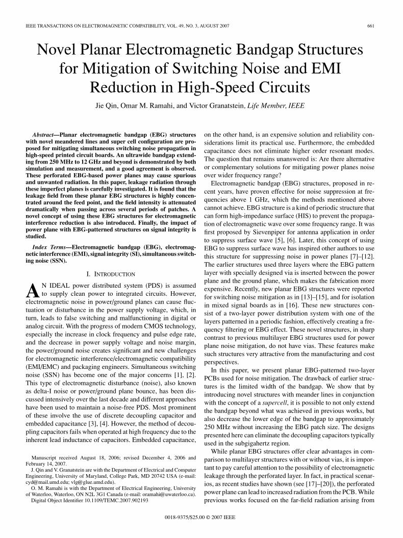
Fig. 1(a) shows the proposed two-layer power/ground planewith meander line EBG structure. The whole dimension of thisstructure with 3× 5 unit cells is 90 mm× 150 mm. The solidlayer can be used for one voltage level, and the EBG-patternedlayer is used for the second voltage level. Between these twolayers, a uniform substrate material FR-4 with dielectric con-stant 4.4 and layer thickness of 1.54 mm is selected due to itsmanufacturing flexibility at our local facilities.
The schematics of the unit cell of size 30 mm× 30 mm, andits corresponding parameters are shown in Fig. 1(b). The dis-tance between the centers of adjacent patches is 30 mm, thepatch width is 28 mm, and the gap between the neighboringpatches is 2 mm. The width of the meandered line is 0.2 mm.For one-dimensional wave propagation, the unit cell of thisMeander-L EBG structure can be modeled with the equivalentcircuit as shown in Fig. 1(c). This qualitative model is inspiredby the physical behavior of the fields in the patch. It consistsof two parts. The first part describes the propagation character-istics between the EBG patch and the continuous power plane,represented by equivalent inductance Lp and capacitance Cp .The second part characterizes the bridge effects between twoadjacent unit cells, where the gap between the two neighboringunit cells induces the fringe capacitance Cb , and the bridge con-necting the neighboring unit cells as the inductor Lb . Thus, thisEBG structure can be conceptually viewed as an electrical filterof parallel LC resonator.
The center frequency of the stop-band for the EBG structurecan be expressed semiquantitatively as f0 = 1/(2π
√(LbCb)).
Consequently, one observes that in order to effectively imple-ment the EBG structure in the lower frequency region, a longerbridge length corresponding to an increase in inductance wouldbe required. Therefore, we introduce a meander line as the con-necting bridge (dc link) between adjacent patches. The width ofthe meandered line is 0.2 mm, which is within the fabricationtolerance capability of our laboratory facility. (The LPKF proto-type machine was used for fabricating the prototypes discussedin this paper.)
Fig. 1. (a) Planar EBG structure with Meander-L bridge showing the locationof the ports used for S21 parameter measurements. (b) Unit cell showing themeander line bridge and dimensions. (c) Qualitative equivalent circuit modelfor unit cell of the Meander-L EBG structure.
B. Simulation and Experimental Result
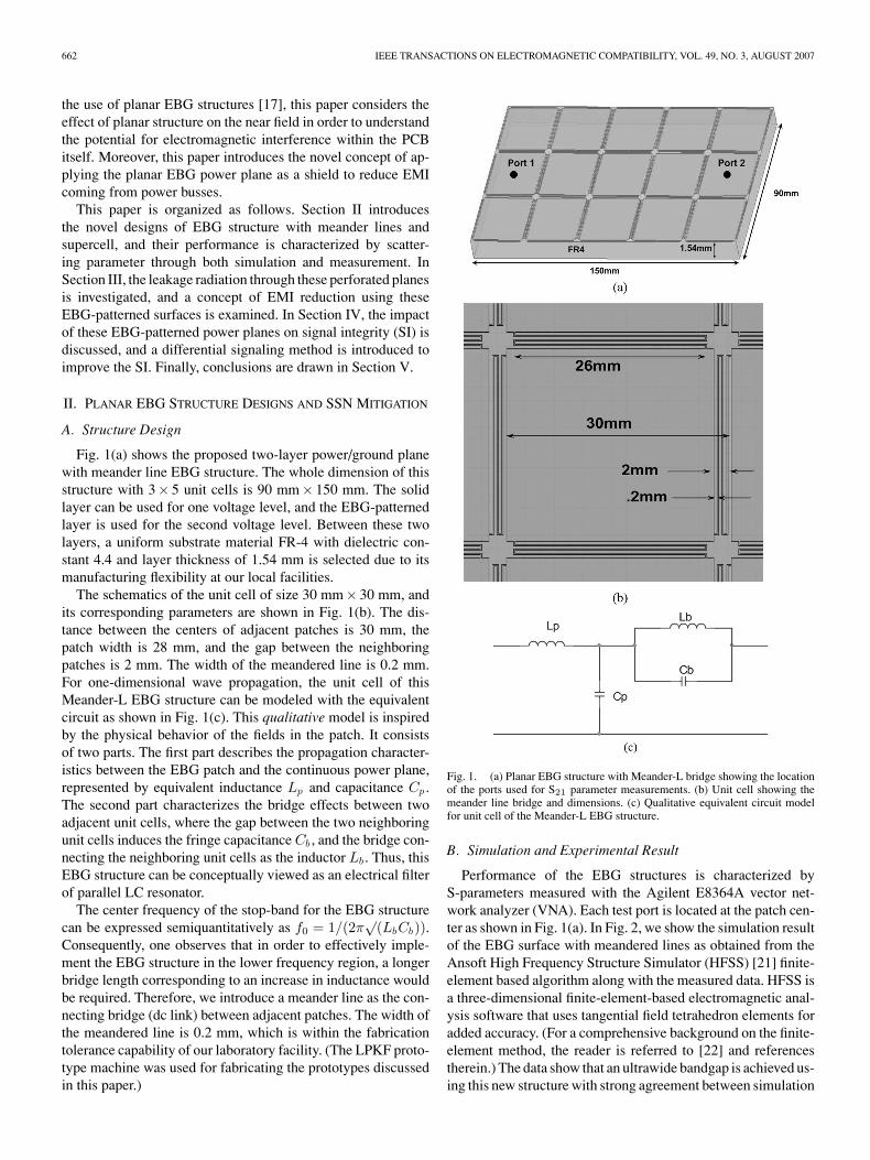
Performance of the EBG structures is characterized byS-parameters measured with the Agilent E8364A vector net-work analyzer (VNA). Each test port is located at the patch cen-ter as shown in Fig. 1(a). In Fig. 2, we show the simulation resultof the EBG surface with meandered lines as obtained from theAnsoft High Frequency Structure Simulator (HFSS) [21] finite-element based algorithm along with the measured data. HFSS isa three-dimensional finite-element-based electromagnetic anal-ysis software that uses tangential field tetrahedron elements foradded accuracy. (For a comprehensive background on the finite-element method, the reader is referred to [22] and referencestherein.) The data show that an ultrawide bandgap is achieved us-ing this new structure with strong agreement between simulation
QIN et al.: NOVEL PLANAR EBG STRUCTURES 663
Fig. 2. Numerical simulation and measurement result for magnitude of S21.
and measurements. The stopband frequency range is observedto extend from approximately 450 MHz to 12 GHz and beyond.The definition of the bandwidth adopted here is the continu-ous frequency range over which the magnitude of the S21 ismaintained below −28 dB. (There is no standard definition forsuppression bandwidth in the context of switching noise as thedegree of suppression is application specific. Here, the −28 dBwas chosen for convenience as it represents significant suppres-sion in comparison to the reference case.)
Next, we introduce the concept of a supercell. The detailmechanism of this structure is discussed in [15]. The basic idea isto create a cell comprising two patches with different topology.The new supercell will then be cascaded resulting in a newstructure that is expected to embody the bandgaps arising fromthe use of each of the two topologies if they were used separately,in addition to the bandgap arising from the periodicity formed bythis new supercell. Fig. 3(a) shows the basic unit of this supercellstructure. It shows adjacent EBG patches with two differentconnecting bridge topologies: a straight line and a meanderline. The patch is kept at the same size of 30 mm× 30 mm. Thefabricated PCB with an overall dimension of 90 mm× 150 mmis shown in Fig. 3(b).
The S21 parameter data (simulation and measurement) isshown in Fig. 4, where we observe not just an appreciably widebandgap but, more importantly, the shift of the lower edge ofthe stopband downward to approximately 250 MHz. This band-width improvement realized by the supercell can lead to costreduction by eliminating the decoupling capacitors needed tomaintain minimal noise in the sub-500-MHz range.
III. RADIATION ANALYSIS
A. Leakage Radiation Through EBG-Patterned PCB
Previous studies show that the radiation from solid powerplanes comes from a time-varying electric field at the boardedges similar to the way a patch antenna radiates [23], [24]. Ifthe signal is fed at one port and received at another port, part ofthe energy radiates at the edge of the board while never reachingany of the other ports. The radiation loss can be characterized bythe quantity 1 − |S11|2 − |S21|2. This is different from a closed
Fig. 3. (a) Schematic top view of the supercell with dimensions. (b) Wholestructure of fabricated PCB showing test ports for S parameter measurement.
Fig. 4. Numerical simulation and measurement of the magnitude of S21 forthe novel structure proposed in this paper (supercell) and for the two-layer powerplane.
lossless system, in which the total combination of reflectioncoefficient and transmission coefficient equals to unity. For theperforated planar EBG structures described earlier, in additionto the radiation at the edges of board, there are gaps betweenthe cells, which may cause extra radiation leakage, especiallyat the frequency where the patches resonate. In sharp contrast tothe three- or multilayer EBG structures with solid power plane,this extra radiation from these perforated boards can potentially
664 IEEE TRANSACTIONS ON ELECTROMAGNETIC COMPATIBILITY, VOL. 49, NO. 3, AUGUST 2007
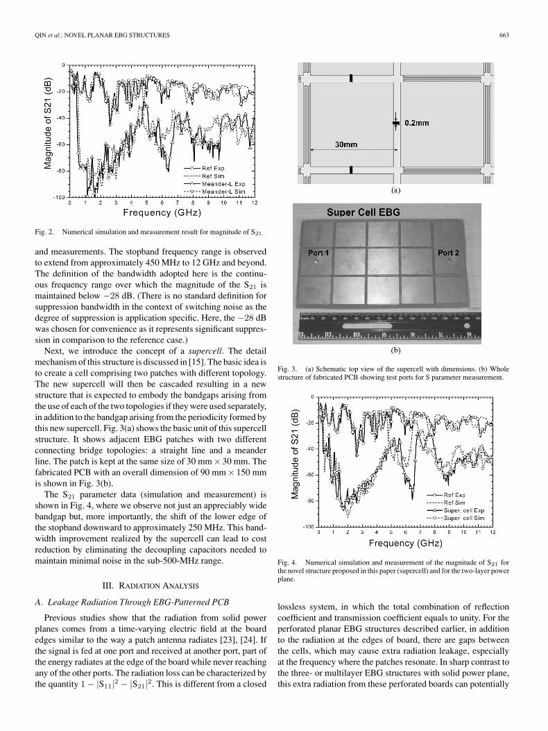
Fig. 5. Radiation loss for different structures.
Fig. 6. Simulated port input impedance for different structures.
be sufficient to create incompatibility with either circuit func-tionality, or simply be high enough to violate regulatory radia-tion standards.
Here, the calculated loss factor 1 − |S11|2 − |S21|2 is exam-ined for EBG-based power planes and compared to the casewith solid power plane. The results shown in Fig. 5 demonstratethat the radiation peaks at 480, 960 MHz, etc., which arise fromthe cavity modes of the 90 mm× 150 mm reference board, aresignificantly suppressed for the EBG-patterned structures. Thestrong radiation peaks at 4.7, 6.6, 9.4, and 10.6 GHz for theEBG-patterned power planes are due to the patch resonance,which can be further confirmed from the input impedance (selfimpedance of excitation port) data shown in Fig. 6, where thefirst high impedance peak corresponds to the f20,02 modes ofthe 30 mm× 30 mm patch at 4.7 GHz followed by even num-bered modes f22, f40. Notice that odd-numbered modes do notappear because the feed port consists of a center-fed patch [25].When the patch is fed off center, the odd-numbered modes ap-pear consistent with the cavity resonance behavior (results arenot shown for brevity).
However, the radiation loss from these impedance peaks doesnot show much increase when comparison is made to the case
Fig. 7. Near-field measurement setup.
of solid reference plane. This is due to the resonance modesoverlap between those of the reference plane and of the singlepatch. Overall, the data show that the total radiated power fromthe EBG-patterned PCB is diminished, especially at the lowerfrequency region (below the fundamental resonance of patch at4.7 GHz) in comparison to the reference plane.
We emphasize here that the measure of the radiation loss usedhere, i.e., the quantity 1 − |S11|2 − |S21|2, is only indicative ofthe fact that the electromagnetic energy prevented from propa-gating between the two ports is either stopped at the source (thetransmitting port, due to a change in its input impedance as aresult of using the EBG patches) or leaks through other chan-nels. A more detailed analysis of the power leakage is given inSection III-B.
B. Near-Field Characterization
In order to obtain a better understanding of the shieldingbehavior of perforated power planes, the near field of these pro-posed planar EBG structures is studied. In all the cases studiedhere, comparison is always made to the fields arising from atwo-layer solid power plane.
The analysis here is carried out by using a monopole antennaconnected to a power meter to monitor the field along a test linepositioned 1 cm above the EBG-patterned plane and alignedalong the open slot of the EBG patches extending from the leftto the right edge (represented by normalized distance) as shownin Fig. 7(a) and (b). An RF signal of 10 dBm is launched into the
QIN et al.: NOVEL PLANAR EBG STRUCTURES 665
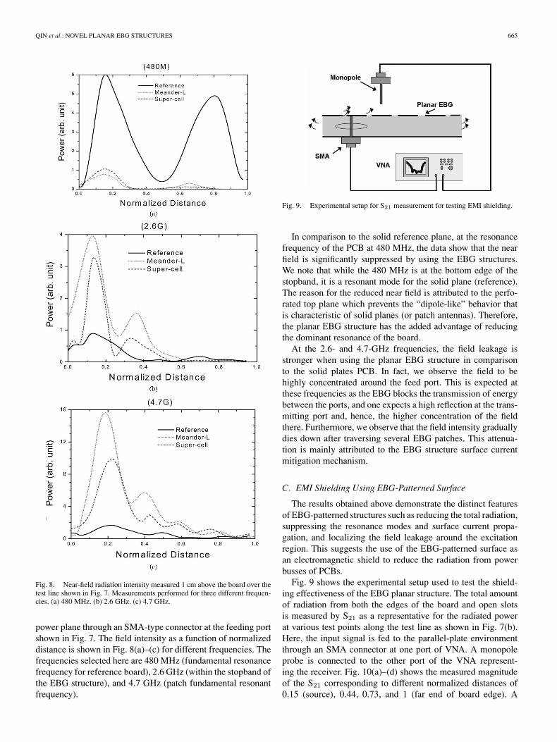
Fig. 8. Near-field radiation intensity measured 1 cm above the board over thetest line shown in Fig. 7. Measurements performed for three different frequen-cies. (a) 480 MHz. (b) 2.6 GHz. (c) 4.7 GHz.
power plane through an SMA-type connector at the feeding portshown in Fig. 7. The field intensity as a function of normalizeddistance is shown in Fig. 8(a)–(c) for different frequencies. Thefrequencies selected here are 480 MHz (fundamental resonancefrequency for reference board), 2.6 GHz (within the stopband ofthe EBG structure), and 4.7 GHz (patch fundamental resonantfrequency).
Fig. 9. Experimental setup for S21 measurement for testing EMI shielding.
In comparison to the solid reference plane, at the resonancefrequency of the PCB at 480 MHz, the data show that the nearfield is significantly suppressed by using the EBG structures.We note that while the 480 MHz is at the bottom edge of thestopband, it is a resonant mode for the solid plane (reference).The reason for the reduced near field is attributed to the perfo-rated top plane which prevents the “dipole-like” behavior thatis characteristic of solid planes (or patch antennas). Therefore,the planar EBG structure has the added advantage of reducingthe dominant resonance of the board.
At the 2.6- and 4.7-GHz frequencies, the field leakage isstronger when using the planar EBG structure in comparisonto the solid plates PCB. In fact, we observe the field to behighly concentrated around the feed port. This is expected atthese frequencies as the EBG blocks the transmission of energybetween the ports, and one expects a high reflection at the trans-mitting port and, hence, the higher concentration of the fieldthere. Furthermore, we observe that the field intensity graduallydies down after traversing several EBG patches. This attenua-tion is mainly attributed to the EBG structure surface currentmitigation mechanism.
C. EMI Shielding Using EBG-Patterned Surface
The results obtained above demonstrate the distinct featuresof EBG-patterned structures such as reducing the total radiation,suppressing the resonance modes and surface current propa-gation, and localizing the field leakage around the excitationregion. This suggests the use of the EBG-patterned surface asan electromagnetic shield to reduce the radiation from powerbusses of PCBs.
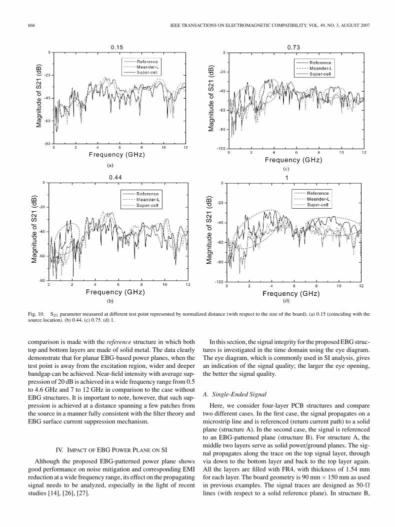
Fig. 9 shows the experimental setup used to test the shield-ing effectiveness of the EBG planar structure. The total amountof radiation from both the edges of the board and open slotsis measured by S21 as a representative for the radiated powerat various test points along the test line as shown in Fig. 7(b).Here, the input signal is fed to the parallel-plate environmentthrough an SMA connector at one port of VNA. A monopoleprobe is connected to the other port of the VNA represent-ing the receiver. Fig. 10(a)–(d) shows the measured magnitudeof the S21 corresponding to different normalized distances of0.15 (source), 0.44, 0.73, and 1 (far end of board edge). A
666 IEEE TRANSACTIONS ON ELECTROMAGNETIC COMPATIBILITY, VOL. 49, NO. 3, AUGUST 2007
Fig. 10. S21 parameter measured at different test point represented by normalized distance (with respect to the size of the board). (a) 0.15 (coinciding with thesource location). (b) 0.44. (c) 0.75. (d) 1.
comparison is made with the reference structure in which bothtop and bottom layers are made of solid metal. The data clearlydemonstrate that for planar EBG-based power planes, when thetest point is away from the excitation region, wider and deeperbandgap can be achieved. Near-field intensity with average sup-pression of 20 dB is achieved in a wide frequency range from 0.5to 4.6 GHz and 7 to 12 GHz in comparison to the case withoutEBG structures. It is important to note, however, that such sup-pression is achieved at a distance spanning a few patches fromthe source in a manner fully consistent with the filter theory andEBG surface current suppression mechanism.
IV. IMPACT OF EBG POWER PLANE ON SI
Although the proposed EBG-patterned power plane showsgood performance on noise mitigation and corresponding EMIreduction at a wide frequency range, its effect on the propagatingsignal needs to be analyzed, especially in the light of recentstudies [14], [26], [27].
In this section, the signal integrity for the proposed EBG struc-tures is investigated in the time domain using the eye diagram.The eye diagram, which is commonly used in SI analysis, givesan indication of the signal quality; the larger the eye opening,the better the signal quality.
A. Single-Ended Signal
Here, we consider four-layer PCB structures and comparetwo different cases. In the first case, the signal propagates on amicrostrip line and is referenced (return current path) to a solidplane (structure A). In the second case, the signal is referencedto an EBG-patterned plane (structure B). For structure A, themiddle two layers serve as solid power/ground planes. The sig-nal propagates along the trace on the top signal layer, throughvia down to the bottom layer and back to the top layer again.All the layers are filled with FR4, with thickness of 1.54 mmfor each layer. The board geometry is 90 mm× 150 mm as usedin previous examples. The signal traces are designed as 50-Ωlines (with respect to a solid reference plane). In structure B,
QIN et al.: NOVEL PLANAR EBG STRUCTURES 667
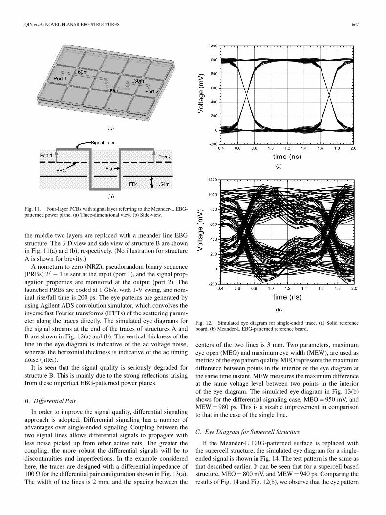
Fig. 11. Four-layer PCBs with signal layer referring to the Meander-L EBG-patterned power plane. (a) Three-dimensional view. (b) Side-view.
the middle two layers are replaced with a meander line EBGstructure. The 3-D view and side view of structure B are shownin Fig. 11(a) and (b), respectively. (No illustration for structureA is shown for brevity.)
A nonreturn to zero (NRZ), pseudorandom binary sequence(PRBs) 27 − 1 is sent at the input (port 1), and the signal prop-agation properties are monitored at the output (port 2). Thelaunched PRBs are coded at 1 Gb/s, with 1-V swing, and nom-inal rise/fall time is 200 ps. The eye patterns are generated byusing Agilent ADS convolution simulator, which convolves theinverse fast Fourier transforms (IFFTs) of the scattering param-eter along the traces directly. The simulated eye diagrams forthe signal streams at the end of the traces of structures A andB are shown in Fig. 12(a) and (b). The vertical thickness of theline in the eye diagram is indicative of the ac voltage noise,whereas the horizontal thickness is indicative of the ac timingnoise (jitter).
It is seen that the signal quality is seriously degraded forstructure B. This is mainly due to the strong reflections arisingfrom these imperfect EBG-patterned power planes.
B. Differential Pair
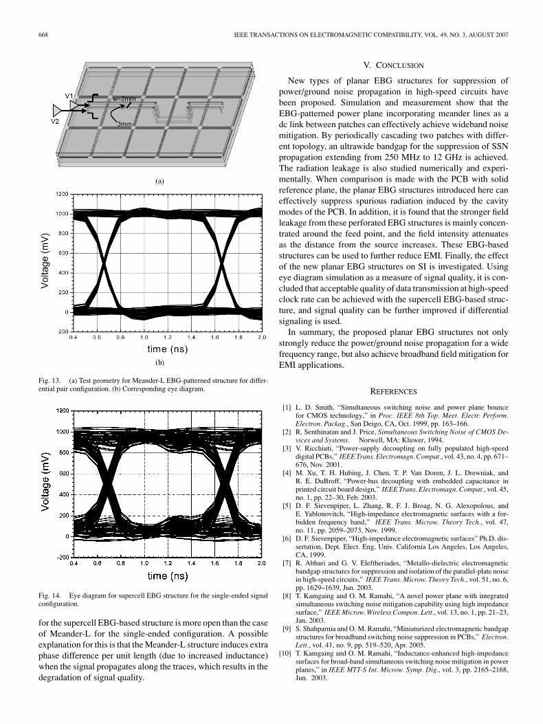
In order to improve the signal quality, differential signalingapproach is adopted. Differential signaling has a number ofadvantages over single-ended signaling. Coupling between thetwo signal lines allows differential signals to propagate withless noise picked up from other active nets. The greater thecoupling, the more robust the differential signals will be todiscontinuities and imperfections. In the example consideredhere, the traces are designed with a differential impedance of100 Ω for the differential pair configuration shown in Fig. 13(a).The width of the lines is 2 mm, and the spacing between the
centers of the two lines is 3 mm. Two parameters, maximumeye open (MEO) and maximum eye width (MEW), are used asmetrics of the eye pattern quality. MEO represents the maximumdifference between points in the interior of the eye diagram atthe same time instant. MEW measures the maximum differenceat the same voltage level between two points in the interiorof the eye diagram. The simulated eye diagram in Fig. 13(b)shows for the differential signaling case, MEO = 950 mV, andMEW = 980 ps. This is a sizable improvement in comparisonto that in the case of the single line.
C. Eye Diagram for Supercell Structure
If the Meander-L EBG-patterned surface is replaced withthe supercell structure, the simulated eye diagram for a single-ended signal is shown in Fig. 14. The test pattern is the same asthat described earlier. It can be seen that for a supercell-basedstructure, MEO = 800 mV, and MEW = 940 ps. Comparing theresults of Fig. 14 and Fig. 12(b), we observe that the eye pattern
668 IEEE TRANSACTIONS ON ELECTROMAGNETIC COMPATIBILITY, VOL. 49, NO. 3, AUGUST 2007
Fig. 13. (a) Test geometry for Meander-L EBG-patterned structure for differ-ential pair configuration. (b) Corresponding eye diagram.
Fig. 14. Eye diagram for supercell EBG structure for the single-ended signalconfiguration.
for the supercell EBG-based structure is more open than the caseof Meander-L for the single-ended configuration. A possibleexplanation for this is that the Meander-L structure induces extraphase difference per unit length (due to increased inductance)when the signal propagates along the traces, which results in thedegradation of signal quality.
V. CONCLUSION
New types of planar EBG structures for suppression ofpower/ground noise propagation in high-speed circuits havebeen proposed. Simulation and measurement show that theEBG-patterned power plane incorporating meander lines as adc link between patches can effectively achieve wideband noisemitigation. By periodically cascading two patches with differ-ent topology, an ultrawide bandgap for the suppression of SSNpropagation extending from 250 MHz to 12 GHz is achieved.The radiation leakage is also studied numerically and experi-mentally. When comparison is made with the PCB with solidreference plane, the planar EBG structures introduced here caneffectively suppress spurious radiation induced by the cavitymodes of the PCB. In addition, it is found that the stronger fieldleakage from these perforated EBG structures is mainly concen-trated around the feed point, and the field intensity attenuatesas the distance from the source increases. These EBG-basedstructures can be used to further reduce EMI. Finally, the effectof the new planar EBG structures on SI is investigated. Usingeye diagram simulation as a measure of signal quality, it is con-cluded that acceptable quality of data transmission at high-speedclock rate can be achieved with the supercell EBG-based struc-ture, and signal quality can be further improved if differentialsignaling is used.
In summary, the proposed planar EBG structures not onlystrongly reduce the power/ground noise propagation for a widefrequency range, but also achieve broadband field mitigation forEMI applications.
REFERENCES
[1] L. D. Smith, “Simultaneous switching noise and power plane bouncefor CMOS technology,” in Proc. IEEE 8th Top. Meet. Electr. Perform.Electron. Packag., San Deigo, CA, Oct. 1999, pp. 163–166.
[2] R. Senthinatan and J. Price, Simultaneous Switching Noise of CMOS De-vices and Systems. Norwell, MA: Kluwer, 1994.
[3] V. Ricchiuti, “Power-supply decoupling on fully populated high-speeddigital PCBs,” IEEE Trans. Electromagn. Compat., vol. 43, no. 4, pp. 671–676, Nov. 2001.
[4] M. Xu, T. H. Hubing, J. Chen, T. P. Van Doren, J. L. Drewniak, andR. E. DuBroff, “Power-bus decoupling with embedded capacitance inprinted circuit board design,” IEEE Trans. Electromagn. Compat., vol. 45,no. 1, pp. 22–30, Feb. 2003.
[5] D. F. Sievenpiper, L. Zhang, R. F. J. Broag, N. G. Alexopolous, andE. Yablonovitch, “High-impedance electromagnetic surfaces with a for-bidden frequency band,” IEEE Trans. Microw. Theory Tech., vol. 47,no. 11, pp. 2059–2073, Nov. 1999.
[6] D. F. Sievenpiper, “High-impedance electromagnetic surfaces” Ph.D. dis-sertation, Dept. Elect. Eng, Univ. California Los Angeles, Los Angeles,CA, 1999.
[7] R. Abhari and G. V. Eleftheriades, “Metallo-dielectric electromagneticbandgap structures for suppression and isolation of the parallel-plate noisein high-speed circuits,” IEEE Trans. Microw. Theory Tech., vol. 51, no. 6,pp. 1629–1639, Jun. 2003.
[8] T. Kamgaing and O. M. Ramahi, “A novel power plane with integratedsimultaneous switching noise mitigation capability using high impedancesurface,” IEEE Microw. Wireless Compon. Lett., vol. 13, no. 1, pp. 21–23,Jan. 2003.
[9] S. Shahparnia and O. M. Ramahi, “Miniaturized electromagnetic bandgapstructures for broadband switching noise suppression in PCBs,” Electron.Lett., vol. 41, no. 9, pp. 519–520, Apr. 2005.
[10] T. Kamgaing and O. M. Ramahi, “Inductance-enhanced high-impedancesurfaces for broad-band simultaneous switching noise mitigation in powerplanes,” in IEEE MTT-S Int. Microw. Symp. Dig., vol. 3, pp. 2165–2168,Jun. 2003.
QIN et al.: NOVEL PLANAR EBG STRUCTURES 669
[11] S. D. Rogers, “Electromagnetic-bandgap layers for broad-band suppres-sion of TEM modes in power planes,” IEEE Trans. Microw. Theory Tech.,vol. 53, no. 8, pp. 2495–2505, Aug. 2005.
[12] S. Shahparnia, B. Mohajer-Iravani, and O. M. Ramahi, “Electromagneticnoise mitigation in high-speed printed circuit boards and packaging usingelectromagnetic bandgap structures,” in Proc. 54th Electron. Compon.Technol. Conf., Las Vegas, NV, Jun. 2004, pp. 1831–1836.
[13] F. R. Yang, K. P. Ma, and T. Itoh, “A uniplanar compact photonic-bandgap(UC-PBG) structure and its applications for microwave circuits,” IEEETrans. Microw. Theory Tech., vol. 47, no. 8, pp. 1509–1514, Aug. 1999.
[14] T. L. Wu, C. C. Yang, Y. H. Lin et al., “A novel power plane with super-wideband elimination of ground bounce noise on high speed circuits,”IEEE Microw Wireless Compon. Lett., vol. 15, no. 3, pp. 174–176, Mar.2005.
[15] J. Qin and O. M. Ramahi, “Ultra-wideband mitigation of simultaneousswitching noise using novel planar electromagnetic bandgap structure,”IEEE Microw. Wireless Compon. Lett., vol. 16, no. 9, pp. 487–489, Sep.2006.
[16] J. Choi, V. Govind, M. Swaminathan, L. Wan, and R. Doraiswami, “Iso-lation in mixed-signal systems using a novel electromagnetic bandgap(EBG) structure,” in Proc. IEEE 13th Top. Meet. Electr. Perform. Elec-tron. Packag., Portland, OR, Oct. 2004, pp. 199–202.
[17] T. L. Wu, Y. H. Lin, and S. T. Chen, “A novel power planes with lowradiation and broadband suppression of ground bounce noise using pho-tonic bandgap structures,” IEEE Microw. Wireless Compon. Lett., vol. 14,no. 7, pp. 337–339, Jul. 2004.
[18] N. Shino and Z. Popovic, “Radiation from ground-plane photonic bandgapmicrostrip waveguide,” IEEE MTT-S Int. Microw. Symp. Dig, vol. 2,pp. 1079–1082, Jun. 2002.
[19] J. Lee, H. Kim, and J. Kim, “High dielectric constant thin film EBGpower/ground network for broad-band suppression of SSN and radiatedemissions,” IEEE Microw. Wireless Compon. Lett., vol. 15, no. 8, pp. 505–507, Aug. 2005.
[20] Y. Ko, K. Ito, J. Kudo, and T. Sudo, “Electromagnetic radiation propertiesof a printed circuit board with a slot in the ground plane,” in Proc. Int.Symp. Electromagn. Compat., Tokyo, Japan, May1999, pp. 576–579.
[21] HFSS, High Frequency Structure Simulator version 9.2, Ansoft Corp.Pittsburgh, PA.
[22] Jianming Jin, The Finite Elements in Electromagnetics. New York:Wiley, 2002.
[23] T. H. Hubing, “Printed circuit board EMI source mechanisms,” in Proc.IEEE Int. Symp. Electromagn. Compat., Boston, MA, Aug. vol. 1, 2003,pp. 1–3.
[24] M. Leone, “The radiation of a rectangular power bus structure at multiplecavity-mode resonances,” IEEE Trans. Electromagn. Compat., vol. 45,no. 3, pp. 486–492, Aug. 2003.
[25] N. Na, J. Choi, S. Chun, M. Swaminathan, and J. Srinivasan, “Modelingand transient simulation of planes in electronic packages,” IEEE Trans.Adv. Packag., vol. 23, no. 3, pp. 340–352, Aug. 2000.
[26] P. Clayton, Introduction to Electromagnetic Compatibility. Hoboken,NJ: Wiley-Interscience, 1992.
[27] J. C. W. Ho, Q. Zhu, and R. Abhari, “Modeling of transmission lineswith textured ground planes and investigation of data transmission bygenerating eye diagrams,” in Proc. IEEE 13th Top. Meet. Electr. Perform.Electron. Packag., Portland, OR, Oct. 2004, pp. 195–198.
Jie Qin received the B.S. degree in electrical engi-neering from Zhejiang University, Hangzhou, China,in 1990, the M.S. degree in electrophysics from theChinese Academy of Science, Beijing, in 1996, andthe Ph.D. degree in electrical and computer engineer-ing from the University of Maryland, College Park,in 2006.
From 1990 to 1997, he was a Research Staff mem-ber in the Xian Institute of Optics and Precision Me-chanics, Chinese Academy of Science. There he madecontributions to several projects in developing new
optoelectronic devices. He then joined the National Key Laboratory of Ap-plied Surface Physics, Fudan University, Shanghai, China, where he carried onresearch on semiconductor microfabrication and nanoelectronics. His currentresearch interests include electromagnetic bandgap structures, design of RF andmicrowave devices, high-speed packaging, and signal integrity.
Omar M. Ramahi received the B.S. degree in math-ematics and electrical and computer engineering(summa cum laude) from Oregon State University,Corvallis, and the M.S. and Ph.D. degrees in electri-cal and computer engineering from the University ofIllinois at Urbana-Champaign, Champaign.
From 1990 to 1993, he was a Visiting Fellow withthe University of Illinois at Urbana-Champaign. From1993 to 2000, he was with the Digital Equipment Cor-poration (presently Hewlett-Packard), Maynard, MA,where he was a member of the Alpha Server Product
Development Group. In August 2000, he joined the faculty of the James ClarkSchool of Engineering, University of Maryland, College Park, where he was alsoa Faculty member of the CALCE Electronic Products and Systems Center. He iscurrently the Associate NSERC/RIM Industrial Research Chair in the Electricaland Computer Engineering Department, University of Waterloo, Waterloo, ON,Canada. He has been a Consultant to several companies and was a cofounder ofEMS-PLUS, Four Oaks, NC, and Applied Electromagnetic Technology, LLC,Solomons, MD. His research interests include experimental and computationalEMI/EMC studies, high-speed devices and interconnects, biomedical applica-tions of electromagnetics, novel optimization techniques, and interdisciplinarystudies linking electromagnetic application to novel materials. He has authoredand coauthored over 150 papers published in several journals and conferenceproceedings, and has coauthored EMI/EMC Computational Modeling Hand-book, 2nd ed. (Springer-Verlag, 2001).
Victor L. Granatstein (S’59–M’64–SM’86–F’92–LF’02) received the Ph.D. degree in electrical en-gineering from Columbia University, New York, in1963.
From 1964 to 1972, he was a Research Scientistwith Bell Telephone Laboratories, Murray Hill, NJ,after a year of postdoctoral work at Columbia Uni-versity. He was a Visiting Senior Lecturer with theHebrew University of Jerusalem, Jerusalem, Israel,in 1969–1970. In 1972, he joined the Naval ResearchLaboratory (NRL), Washington, DC, as a Research
Physicist, where he was the Head of NRL’s High Power Electromagnetic Ra-diation Branch from 1978 to 1983. Since August 1983, he has been a Pro-fessor in the Electrical and Computer Engineering Department, University ofMaryland, College Park. From 1987 to1998, he was the Director of the Institutefor Plasma Research (now renamed Institute for Research in Electronics andApplied Physics), University of Maryland. He was a Visiting Professor at TelAviv University, Tel Aviv, Israel, in 1994 and 2003, where he became the Sack-ler Professor by Special Appointment in 2004. His current research interestsinclude electromagnetic radiation from relativistic electron beams, advancedconcepts in millimeter wave tubes, and the effects of high-power microwaveson electronic circuits and systems. He has coauthored more than 250 researchpapers in several scientific journals and has coedited three books. He holds anumber of patents on active and passive microwave devices.
Dr. Granatstein is a Fellow of the American Physical Society. He has receiveda number of major research awards including the E.O. Hulbert Annual ScienceAward in 1979, the Superior Civilian Service Award in 1980, the Captain RobertDexter Conrad Award for scientific achievement awarded by the Secretary ofthe Navy in 1981, the IEEE Plasma Science and Applications Award in 1991,and the Robert L. Woods Award for Excellence in Electronics Technology in1998.


![512 IEEE TRANSACTIONS ON ELECTROMAGNETIC COMPATIBILITY ... · 514 IEEE TRANSACTIONS ON ELECTROMAGNETIC COMPATIBILITY, VOL. 58, NO. 2, APRIL 2016 dimensionless quantities [27] corresponding](https://static.documents.pub/doc/80x56/5f09f2a07e708231d42945f5/512-ieee-transactions-on-electromagnetic-compatibility-514-ieee-transactions.jpg)


