IEEE TRANSACTIONS ON NEURAL NETWORKS, VOL. 20, NO. 9, SEPTEMBER 2009 1417
CAVIAR: A 45k Neuron, 5M Synapse, 12GConnects/s AER Hardware Sensory–Processing–
Learning–Actuating System for High-SpeedVisual Object Recognition and Tracking
Rafael Serrano-Gotarredona, Matthias Oster, Patrick Lichtsteiner, Alejandro Linares-Barranco,Rafael Paz-Vicente, Francisco Gómez-Rodríguez, Luis Camuñas-Mesa, Raphael Berner, Manuel Rivas-Pérez,
Tobi Delbrück, Shih-Chii Liu, Rodney Douglas, Philipp Häfliger, Gabriel Jiménez-Moreno, Anton Civit Ballcels,Teresa Serrano-Gotarredona, Member, IEEE, Antonio J. Acosta-Jiménez, and Bernabé Linares-Barranco
Abstract—This paper describes CAVIAR, a massively par-allel hardware implementation of a spike-based sensing–pro-cessing–learning–actuating system inspired by the physiology ofthe nervous system. CAVIAR uses the asychronous address–eventrepresentation (AER) communication framework and was de-veloped in the context of a European Union funded project. Ithas four custom mixed-signal AER chips, five custom digitalAER interface components, 45k neurons (spiking cells), up to5M synapses, performs 12G synaptic operations per second, andachieves millisecond object recognition and tracking latencies.
Manuscript received June 29, 2008; revised November 11, 2008 and April 06,2009; accepted April 24, 2009. First published July 24, 2009; current versionpublished September 02, 2009. This work was supported by the European Com-mission under Grant IST-2001-34124 (CAVIAR). The work of R. Serrano-Go-tarredona was supported by the Spanish Ministry of Education and Scienceunder FPU scholarship. The work of L. Camuñas-Mesa was supported by theSpanish Ministry of Education and Science under FPI scholarship. The work ofS.-C. Liu and T. Delbrück was supported by the Institute of Neuroinformatics(INI), ETH Zürich/University of Zürich, Zürich, Switzerland and some fabrica-tion costs were paid by Austria Research Corporation.
R. Serrano-Gotarredona was with the Consejo Superior de InvestigacionesCientificas, Seville Microelectronics Institute, Seville 41012, Spain. He is nowwith the Austriamicrosystems, Valencia, Spain (e-mail: [email protected]).
M. Oster was with the Institute of Neuroinformatics (INI), ETH Zürich/Uni-versity of Zürich, Zürich CH-8057, Switzerland. He is now with the VarianMedical Systems, Baden CH-5405, Switzerland (e-mail: [email protected]).
P. Lichtsteiner was with the Institute of Neuroinformatics (INI), ETH Zürich/University of Zürich, Zürich CH-8057, Switzerland. He is now with the Es-pros Photonics Corporation, Baar CH-6340, Switzerland (e-mail: [email protected]).
L. Camuñas-Mesa, T. Serrano-Gotarredona, A. Acosta-Jiménez, and B.Linares-Barranco are with the Consejo Superior de Investigaciones Ci-entificas, Seville Microelectronics Institute, Seville 41092, Spain (e-mail:[email protected]; [email protected]; [email protected];[email protected]).
P. Häfliger is with the Informatics, University of Oslo, Oslo NO-0316,Norway (e-mail: [email protected]).
Color versions of one or more of the figures in this paper are available onlineat http://ieeexplore.ieee.org.
Digital Object Identifier 10.1109/TNN.2009.2023653
Index Terms—Address–event representation (AER), neuromor-phic chips, neuromorphic systems, vision.
I. INTRODUCTION
B RAINS perform powerful and fast vision processing in away conceptually different from that of machine vision
systems. Machine vision systems process sequences of stillframes from a camera. For performing scale- and rotation-in-variant 3-D object recognition, for example, sequences ofcomputationally demanding operations need to be performedon each acquired frame. The computational power and speedrequired for such tasks make it difficult to develop real-timeautonomous systems for such applications.
On the other hand, vision sensing and object recognition inbrains are performed without using the “frame” concept, at leastnot in the usual sense of implying a fixed-rate sequence of stillimages. Throughout this paper, we intentionally avoid the useof the expression “image processing,” because in our hardwaretechnology, there never is an “image” or a “frame,” but rather acontinuous flow of visual information in the form of temporalspikes.
The visual cortex is structured as a sequence of layers (8–10layers in the human cortex [1], [13]), starting from the retina,which does its own preprocessing in a more compact and analogarchitecture. Although cortex has massive feedback and recur-rent connections, it is known that a very fast and purely feed-forward recognition path exists within the ventral stream of thevisual cortex [1], [2]. Here we exploited this feedforward pathconcept to build a fast vision recognition system. A concep-tual block diagram of such a cortically inspired feedforwardhierarchically structured autonomous system for sensing/pro-cessing/decision–actuation can be seen in Fig. 1(a) [1]–[11].The pattern of connectivity in cortex follows a basic structure:each neuron in a layer connects to a “cluster of neurons” or “pro-jective field” in the next layer [12], [13].
In most cases, these projective fields can be approximated bycomputing 2-D convolutions. A single layer of a single con-volution kernel can detect and localize a preprogrammed orprelearned object, independent of its position. Using multiple
1418 IEEE TRANSACTIONS ON NEURAL NETWORKS, VOL. 20, NO. 9, SEPTEMBER 2009
kernels of different sizes and rotations can make the compu-tation scale and rotation invariant. Multilayered convolutionalnetworks are capable of complex object recognition [3]–[8].
Spiking neurons receive synaptic input from other cells in theform of electrical spikes, and they autonomously decide whento generate their own output spikes. Hardware that combinesspike-based multineuron modules to compute projective fieldscan enable powerful and fast frame-free vision processing. If thecomponents generate short-latency meaningful, nonredundantspikes, then spike-based systems can efficiently compute “on-demand” compared to conventional approaches. The processingdelay depends mainly on the number of layers, and not on thecomplexity of objects and shapes to be recognized. Their latencyand throughput are not limited by a conventional samplingrate.
In recent years, significant progress has been made towardsthe understanding of the computational principles exploited byvisual cortex. Many artificial systems that implement bioin-spired software models use biological-like (convolution-based)processing that outperforms more conventionally engineeredmachines [3]–[11], [14]–[17]. However, these systems gen-erally run at extremely low speeds because the models areimplemented as software programs on conventional computers.For real-time solutions, direct hardware implementations ofthese models are required. However, hardware engineers facea large hurdle when trying to mimic the bioinspired layeredstructure and the massive connectivity within and betweenlayers. A growing number of research groups worldwide aremapping some of these computational principles onto real-timespiking hardware through the development and exploitation ofthe so-called address–event representation (AER) technology.In this paper, we report on the results of our European Unionconsortium project “Convolution AER Vision Architecture forReal-Time” (CAVIAR), where the largest ever built multichipmultilayer AER real-time frame-free vision system to date hasbeen developed.
The purpose of this paper is to introduce to various commu-nities, including computational neuroscience and machine vi-sion, the promising and effective AER hardware technology thatallows the construction of modular, multilayered, hierarchical,and scalable (visual) sensory processing learning and actuatingsystems. Throughout this paper, we will illustrate the power andpotential of the AER hardware technology through the demon-strator assembled in the CAVIAR project.
The AER is a spike-based representation technique forcommunicating asynchronous spikes between layers of neuronsin different chips. The spikes in AER are carried as addresses ofsending or receiving neurons on a digital bus. Time “representsitself” as the asynchronous occurrence of the event. AER wasfirst proposed in 1991 by Mead’s Lab at California Instituteof Technology (Caltech, Pasadena) [24]–[28], and has beenused since then by a wide community of hardware engineers.Unarbitrated and simpler event readout have been used [29],[30], and more elaborate and efficient arbitrated versions havealso been proposed, based on winner-take-all (WTA) [31],or the use of arbiter trees [32], which have evolved to rowparallel [33] and burst-mode word-serial [34]–[36] readoutschemes by Boahen’s Lab. The AER has been used in image
and vision sensors, for simple light intensity to frequencytransformations [38], time-to-first-spike codings [40]–[42],foveated sensors [43], [44], spatial contrast sensors [23],[45], temporal intensity difference [39] and temporal contrastsensors [19], [20], and motion sensing and computation systems[46]–[50]. AER has also been used for auditory systems[51]–[53], competition and WTA networks [54]–[56], andeven for systems distributed over wireless networks [57]. ForAER-based 2-D convolution, Vernier et al. [58] and Choi et al.[59] reported on 2-D convolution chips with hard-wired ellipticor Gabor-shaped kernels for orientation extraction. AER hasmade it feasible to emulate large scale neurocortical-likemultilayered realistic structures since the development ofscalable and reprogrammable kernel 2-D convolution chips,either with some minor restrictions on symmetry [60], orwithout any restrictions on shape or size [18]. Of greatimportance for the spread and success of AER systems has alsobeen the availability of open-source reusable silicon IP [37], abetter understanding by the community of asynchronous logicdesign, and the development of conventional synchronousinterfacing logic and computer interfaces [61]–[64].
In CAVIAR, an AER infrastructure was developed to supporta set of AER modules (chips and interfaces) [Fig. 1(b)] that areconnected in series and parallel to embody the abstract layeredarchitecture in Fig. 1(a). The following modules were devel-oped: 1) a temporal contrast retina (motion sensing camera)chip; 2) a programmable kernel 2-D convolution processingchip; 3) a 2-D WTA object chip; 4) spatio–temporal processingand learning chips; 5) AER remapping, splitting, and mergingfield-programmable gate array (FPGA)-based modules; and6) computer–AER interfacing FPGA modules for generatingand/or capturing AER. These modules were then used forbuilding a multilayer artificial vision demonstrator system fordetecting and tracking balls moving at high speeds.
The overall architecture of the CAVIAR vision system is il-lustrated in Fig. 1(b) and in more detail in Fig. 13. Movingobjects in the field of view of the retina cause spikes. Eachspike from the retina causes a splat of each convolution chip’skernel onto its own integrator array. When the integrator arraypixels exceed positive or negative thresholds they in turn emitspikes. In the CAVIAR system experiments, we generally usedcircular kernels such as the ones in Fig. 3(c) and (d), which de-tect circular objects of particular sizes. The resulting convolu-tion spike outputs are noise filtered by the WTA object chip.The WTA output spikes, whose addresses represent the loca-tion of the “best” circular object, are fed into a configurabledelay line chip that spreads time into space. This spatial pat-tern of temporal delayed spikes is then learned by the learningchip. The WTA spikes also control a mechanical or electronictracking system that stabilizes the programmed object in thefield-of-view center.
The rest of this paper is structured as follows. Section IIdescribes the temporal contrast retina, Section III the pro-grammable kernel 2-D convolution chip, Section IV the 2-DWTA chip, Section V the learning chips, Section VI thedifferent interfaces, and finally, Section VII describes the com-plete CAVIAR vision system and shows experimental results.Section VIII concludes the paper and gives future outlooks.
SERRANO-GOTARREDONA et al.: CAVIAR: A 45K NEURON, 5M SYNAPSE, 12G CONNECTS/S AER HARDWARE 1419
Fig. 1. CAVIAR system overview. (a) A bioinspired system architecture performing feedforward sensing � processing � actuation tends to have the followingconceptual hierarchical structure: 1) a sensing layer; 2) a set of low-level processing layers usually implemented through projection fields (convolutions) for featureextraction and combination; 3) a set of high level processing layers that operate on “abstractions” and progressively compress information through, for example,dimension reduction, competition, and learning; 4) once a reduced set of signals/decisions is obtained they are conveyed to (usually mechanical) actuators. (b)The CAVIAR system components and multilayer architecture; an example output of each component is shown in response to the rotating stimulus and the basicfunctionality is illustrated below each chip component.
TABLE ITEMPORAL CONTRAST VISION SENSOR PROPERTIES ADAPTED FROM [20]
II. AER TEMPORAL CONTRAST RETINA
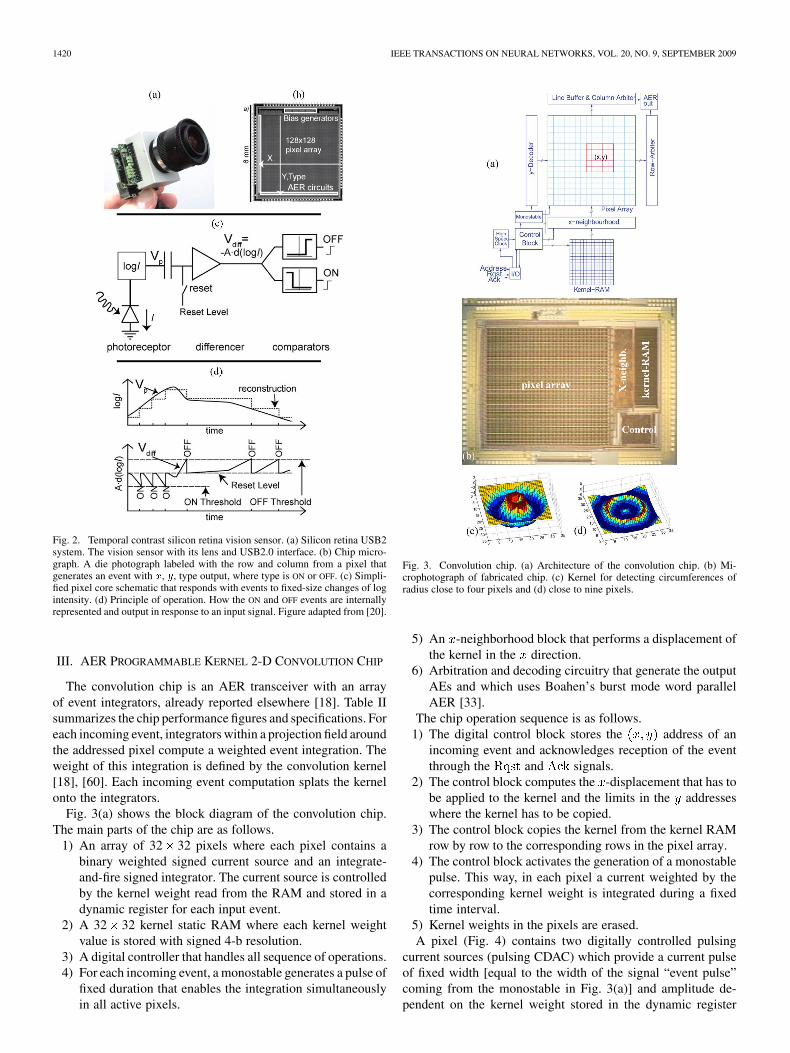
The temporal contrast silicon retina is an asynchronous vi-sion sensor that emits spike address–events (AEs) (Fig. 2 andTable I) [19], [20]. Each AE from the chip is the address of apixel and signifies that the log intensity at pixel changed by anamount since the last event from that pixel. is a global eventthreshold that we typically set to about 15% contrast. In addi-tion, one bit of the address encodes the sign of the change (ON
or OFF). This representation of “change in log intensity” gen-erally encodes scene reflectance change. The compressive log-arithmic transformation in each pixel allows for wide dynamicrange operation (120 dB, compared with for example, 60 dBfor a high-quality traditional image sensor). This wide dynamic
TABLE IICONVOLUTION CHIP PROPERTIES
range means that the sensor can be used with uncontrolled nat-ural lighting. The asynchronous response property also meansthat the events have a latency down to 15 s with bright lightingand typically about 1 ms under indoor illumination, resulting inan effective frame rate of typically several kilohertz. The tem-poral redundancy reduction greatly reduces the output data ratefor scenes in which most pixels are not changing. The design ofthe pixel also allows for unprecedented uniformity of response:the mismatch between pixel contrast thresholds is 2.1% con-trast. The event threshold can be set down to 10% contrast, al-lowing the device to sense natural scenes rather than only artifi-cial high-contrast stimuli. The vision sensor also has integrateddigitally controlled biases that greatly reduce chip-to-chip vari-ation in parameters and temperature sensitivity [21].
1420 IEEE TRANSACTIONS ON NEURAL NETWORKS, VOL. 20, NO. 9, SEPTEMBER 2009
Fig. 2. Temporal contrast silicon retina vision sensor. (a) Silicon retina USB2system. The vision sensor with its lens and USB2.0 interface. (b) Chip micro-graph. A die photograph labeled with the row and column from a pixel thatgenerates an event with �, �, type output, where type is ON or OFF. (c) Simpli-fied pixel core schematic that responds with events to fixed-size changes of logintensity. (d) Principle of operation. How the ON and OFF events are internallyrepresented and output in response to an input signal. Figure adapted from [20].
III. AER PROGRAMMABLE KERNEL 2-D CONVOLUTION CHIP
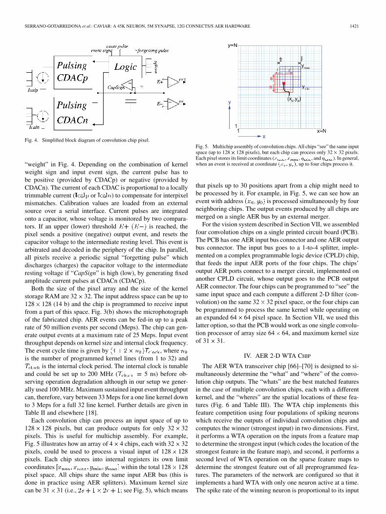
The convolution chip is an AER transceiver with an arrayof event integrators, already reported elsewhere [18]. Table IIsummarizes the chip performance figures and specifications. Foreach incoming event, integrators within a projection field aroundthe addressed pixel compute a weighted event integration. Theweight of this integration is defined by the convolution kernel[18], [60]. Each incoming event computation splats the kernelonto the integrators.
Fig. 3(a) shows the block diagram of the convolution chip.The main parts of the chip are as follows.
1) An array of 32 32 pixels where each pixel contains abinary weighted signed current source and an integrate-and-fire signed integrator. The current source is controlledby the kernel weight read from the RAM and stored in adynamic register for each input event.
2) A 32 32 kernel static RAM where each kernel weightvalue is stored with signed 4-b resolution.
3) A digital controller that handles all sequence of operations.4) For each incoming event, a monostable generates a pulse of
fixed duration that enables the integration simultaneouslyin all active pixels.
Fig. 3. Convolution chip. (a) Architecture of the convolution chip. (b) Mi-crophotograph of fabricated chip. (c) Kernel for detecting circumferences ofradius close to four pixels and (d) close to nine pixels.
5) An -neighborhood block that performs a displacement ofthe kernel in the direction.
6) Arbitration and decoding circuitry that generate the outputAEs and which uses Boahen’s burst mode word parallelAER [33].
The chip operation sequence is as follows.1) The digital control block stores the address of an
incoming event and acknowledges reception of the eventthrough the and signals.
2) The control block computes the -displacement that has tobe applied to the kernel and the limits in the addresseswhere the kernel has to be copied.
3) The control block copies the kernel from the kernel RAMrow by row to the corresponding rows in the pixel array.
4) The control block activates the generation of a monostablepulse. This way, in each pixel a current weighted by thecorresponding kernel weight is integrated during a fixedtime interval.
5) Kernel weights in the pixels are erased.A pixel (Fig. 4) contains two digitally controlled pulsing
current sources (pulsing CDAC) which provide a current pulseof fixed width [equal to the width of the signal “event pulse”coming from the monostable in Fig. 3(a)] and amplitude de-pendent on the kernel weight stored in the dynamic register
SERRANO-GOTARREDONA et al.: CAVIAR: A 45K NEURON, 5M SYNAPSE, 12G CONNECTS/S AER HARDWARE 1421
Fig. 4. Simplified block diagram of convolution chip pixel.
“weight” in Fig. 4. Depending on the combination of kernelweight sign and input event sign, the current pulse has tobe positive (provided by CDACp) or negative (provided byCDACn). The current of each CDAC is proportional to a locallytrimmable current ( or ) to compensate for interpixelmismatches. Calibration values are loaded from an externalsource over a serial interface. Current pulses are integratedonto a capacitor, whose voltage is monitored by two compara-tors. If an upper (lower) threshold is reached, thepixel sends a positive (negative) output event, and resets thecapacitor voltage to the intermediate resting level. This event isarbitrated and decoded in the periphery of the chip. In parallel,all pixels receive a periodic signal “forgetting pulse” whichdischarges (charges) the capacitor voltage to the intermediateresting voltage if “CapSign” is high (low), by generating fixedamplitude current pulses at CDACn (CDACp).
Both the size of the pixel array and the size of the kernelstorage RAM are 32 32. The input address space can be up to128 128 (14 b) and the chip is programmed to receive inputfrom a part of this space. Fig. 3(b) shows the microphotographof the fabricated chip. AER events can be fed-in up to a peakrate of 50 million events per second (Meps). The chip can gen-erate output events at a maximum rate of 25 Meps. Input eventthroughput depends on kernel size and internal clock frequency.The event cycle time is given by , whereis the number of programmed kernel lines (from 1 to 32) and
is the internal clock period. The internal clock is tunableand could be set up to 200 MHz ( 5 ns) before ob-serving operation degradation although in our setup we gener-ally used 100 MHz. Maximum sustained input event throughputcan, therefore, vary between 33 Meps for a one line kernel downto 3 Meps for a full 32 line kernel. Further details are given inTable II and elsewhere [18].
Each convolution chip can process an input space of up to128 128 pixels, but can produce outputs for only 32 32pixels. This is useful for multichip assembly. For example,Fig. 5 illustrates how an array of 4 4 chips, each with 32 32pixels, could be used to process a visual input of 128 128pixels. Each chip stores into internal registers its own limitcoordinates within the total 128 128pixel space. All chips share the same input AER bus (this isdone in practice using AER splitters). Maximum kernel sizecan be 31 31 (i.e., ; see Fig. 5), which means
Fig. 5. Multichip assembly of convolution chips. All chips “see” the same inputspace (up to 128� 128 pixels), but each chip can process only 32� 32 pixels.Each pixel stores its limit coordinates (� ,� , � , and � ). In general,when an event is received at coordinate �� � � �, up to four chips process it.
that pixels up to 30 positions apart from a chip might need tobe processed by it. For example, in Fig. 5, we can see how anevent with address is processed simultaneously by fourneighboring chips. The output events produced by all chips aremerged on a single AER bus by an external merger.
For the vision system described in Section VII, we assembledfour convolution chips on a single printed circuit board (PCB).The PCB has one AER input bus connector and one AER outputbus connector. The input bus goes to a 1-to-4 splitter, imple-mented on a complex programmable logic device (CPLD) chip,that feeds the input AER ports of the four chips. The chips’output AER ports connect to a merger circuit, implemented onanother CPLD circuit, whose output goes to the PCB outputAER connector. The four chips can be programmed to “see” thesame input space and each compute a different 2-D filter (con-volution) on the same 32 32 pixel space, or the four chips canbe programmed to process the same kernel while operating onan expanded 64 64 pixel space. In Section VII, we used thislatter option, so that the PCB would work as one single convolu-tion processor of array size 64 64, and maximum kernel sizeof 31 31.
IV. AER 2-D WTA CHIP
The AER WTA transceiver chip [66]–[70] is designed to si-multaneously determine the “what” and “where” of the convo-lution chip outputs. The “whats” are the best matched featuresin the case of multiple convolution chips, each with a differentkernel, and the “wheres” are the spatial locations of these fea-tures (Fig. 6 and Table III). The WTA chip implements thisfeature competition using four populations of spiking neuronswhich receive the outputs of individual convolution chips andcomputes the winner (strongest input) in two dimensions. First,it performs a WTA operation on the inputs from a feature mapto determine the strongest input (which codes the location of thestrongest feature in the feature map), and second, it performs asecond level of WTA operation on the sparse feature maps todetermine the strongest feature out of all preprogrammed fea-tures. The parameters of the network are configured so that itimplements a hard WTA with only one neuron active at a time.The spike rate of the winning neuron is proportional to its input
1422 IEEE TRANSACTIONS ON NEURAL NETWORKS, VOL. 20, NO. 9, SEPTEMBER 2009
Fig. 6. Layout and architecture of WTA object chip. (a) Architecture and underlying layout of the four populations or quadrants receiving inputs from fourconvolution chips. (b) The architecture of one of the quadrants, each with 256 neurons. Notice that (a) does not show the inputs to the global inhibitory neurons 2.
spike rate. The 2-D WTA chip reduces the data flow rate to thelearning chip by preserving only information about the locationsof the best matched features. The learning chip can then, for ex-ample, track the 3-D movement of an object in space by pro-gramming the same feature shape at different sizes in the dif-ferent convolution chips.
The WTA chip has an array of integrate-and-fire neuronsthat can be configured into four populations or quadrants of16 16 neurons or a single population of 32 32 neurons.Fig. 6(a) shows the network architecture and the underlyinglayout of the four population quadrants. Each quadrant asshown in Fig. 6(b) has 254 excitatory neurons (unfilled circles)and two global inhibitory neurons. The excitatory neuronsreceive external AER inputs representing its feature map from aconvolution chip through four input synapses, which compriseone excitatory synapse, one excitatory depressing synapse [71],and two inhibitory synapses1 (only two of the four synapsesare shown for an exemplar neuron in each quadrant in Fig. 6).The connectivity across the four quadrants can be configuredto enable WTA competition within a feature map (first levelof competition) and across feature maps (second level ofcompetition). Each excitatory neuron also has two sets of localnon-AER synapses which form the connections to and fromglobal inhibitory neurons 1 and 2, and a local self-excitatorysynapse. To enable WTA competition within a feature map orquadrant, the excitatory neurons in that quadrant are configuredto drive their global inhibitory neuron labeled 1 [solid blackcircle in Fig. 6(b)], which in return inhibits these excitatoryneurons. To additionally enable WTA competition acrossfeature maps, the global inhibitory neuron labeled 2 [solidgray (red) circle in Fig. 6(b)] in a quadrant is excited by theglobal inhibitory neurons labeled 1 from the remaining threequadrants. In return, it inhibits all excitatory neurons within itsown quadrant. The second-level competition works as follows.The activity of the global inhibitory neuron 1 in each quadrantreflects the highest input rate to the excitatory neurons withinthe quadrant in the case of a hard WTA competition. Thus,
1In the CAVIAR system described in this paper, we only use the excitatorysynapse. The other three synapses were included for other eventual applications.
TABLE IIIWTA CHIP SPECIFICATIONS
this neuron will activate the global inhibitory neurons 2 of theremaining three quadrants the most if its quadrant receivesthe highest input rate out of the four quadrants. Hence, it canindirectly suppress the activity of the excitatory neurons of theremaining quadrants through their global inhibitory neuron 2.This computation is discussed in detail in [67].
An on-chip global digital-to-analog converter (DAC) blockallows us to set individual local synaptic parameters for eachneuron by using part of the address space to transmit the DACvalue. This block was also used to decrease the amount of mis-match across the neurons. The spiking activity of the neurons ismonitored through the addresses of the output AER spikes whilean on-chip scanner [72] consisting of a clocked set of shift regis-ters allows us to monitor the membrane potentials of the neuronsexternally.
During the WTA operation, each excitatory input spikecharges the membrane of the postsynaptic neuron until oneneuron in the array—the winner—reaches threshold and isreset. All other neurons are then inhibited via the globalinhibitory neuron of its population. Self-excitation provideshysteresis for the winning neuron by facilitating the selectionof this neuron as the next winner.
Because of the moving stimulus, the network must determinethe winner using a rapid estimate of the instantaneous inputfiring rates. The number of spikes that the neuron must integratebefore eliciting an output spike can be adjusted by varying the
SERRANO-GOTARREDONA et al.: CAVIAR: A 45K NEURON, 5M SYNAPSE, 12G CONNECTS/S AER HARDWARE 1423
Fig. 7. Block diagram of the delay line chip.
Fig. 8. Block diagram of the learning chip.
Fig. 9. Die photographs of (a) delay line and (b) learning chips.
strengths of the input synapses. The neuron and synapse param-eters must be programmed appropriately for the incoming inputspike rate to the neurons and the duration of the input so that thenetwork operates properly as a WTA network. The WTA circuitcan reliably select the winner given a difference of input firingrate of only 10% if it receives stationary input spike trains witha regular firing rate. A quantitative analysis of the constraintson the parameter space in regards to a spiking WTA system re-ceiving spiking inputs of various statistics is described in [66],[69], and [70]. These constraints have been derived for the con-dition of a hard WTA network in the case of both regular andPoisson input spike trains. Specifications of the WTA chip aresummarized in Table III.
V. AER LEARNING CHIPS
The learning system in the CAVIAR processing chain sup-plies the ability to learn to classify spatio–temporal patterns rep-resenting the trajectory of a moving object [73]. It is capableof both spike-based learning (or spike-timing-dependent plas-ticity [82]) to learn to classify spatio–temporal spike patternsand rate-based Hebbian learning to learn spatio–temporal ac-tivity patterns. This is achieved in a two-chip AER processing
TABLE IVDELAY LINE CHIP SPECIFICATIONS
system. The first chip expands the time axis of dynamic spatialpatterns into a spatial dimension by simply generating multiplecopies of the pattern at different time delays. In this AER frame-work, this is realized with a delay line chip. The second chip im-plements competitive learning to classify spatial patterns. Thepatterns may be spike patterns, formed by coincident spikes atdifferent spatial locations, or activity patterns, formed by coin-cident average spiking activity at different locations.
A. Expanding Time Into Space
The delay line chip (Figs. 7 and 9 and Table IV) expands timeinto a spatial dimension. It is composed of an asynchronousdelay line with 14 080 delay elements (triangles) and 880 ad-dressable access points. Higher order bits in the address eventsdetermine if one is injecting an event or closing oropening a switch . Output address events are producedat points . Thus, the delay line can be programmed to beclipped at the access points into several delay lines.
Expanding time into a spatial dimension is what we do all thetime as we plot graphs with a time axis. Fig. 16 illustrates thiswith the outputs of the retina, convolution, and WTA stages asthey track a circle on a rotating disk. By representing time inspace, the 2-D motion can be represented in a 3-D figure wherethe circular motion of the circle’s center forms a spiral. Theresult is a snapshot of the circle trajectory within a time window.
B. From Spike-Based to Rate-Based Hebbian Learning
The learning chip (Figs. 8 and 9 and Table V) is an imple-mentation of a spike-based timing-dependent learning rule. Itcontains 32 neurons, each with 64 learning synapses, and aninhibitory and excitatory nonlearning synapse. In the sense ofspike-timing-dependent plasticity the chip can be tuned to in-crease synaptic weights when presynaptic spikes precede post-synaptic spikes within a certain time window. This time windowmay be prolonged and then the net behavior of the synapse be-comes rate dependent, rather than spike timing dependent (giventhat the inputs are roughly Poisson distributed spike trains, see,for example, [73] and [74]). The learning rule as given in [73] is
(1)
This learning rule implicitly normalizes the weight vector tolength , which is a free parameter, that is, any attractor of thedynamics of has length . Another parameter is the learning
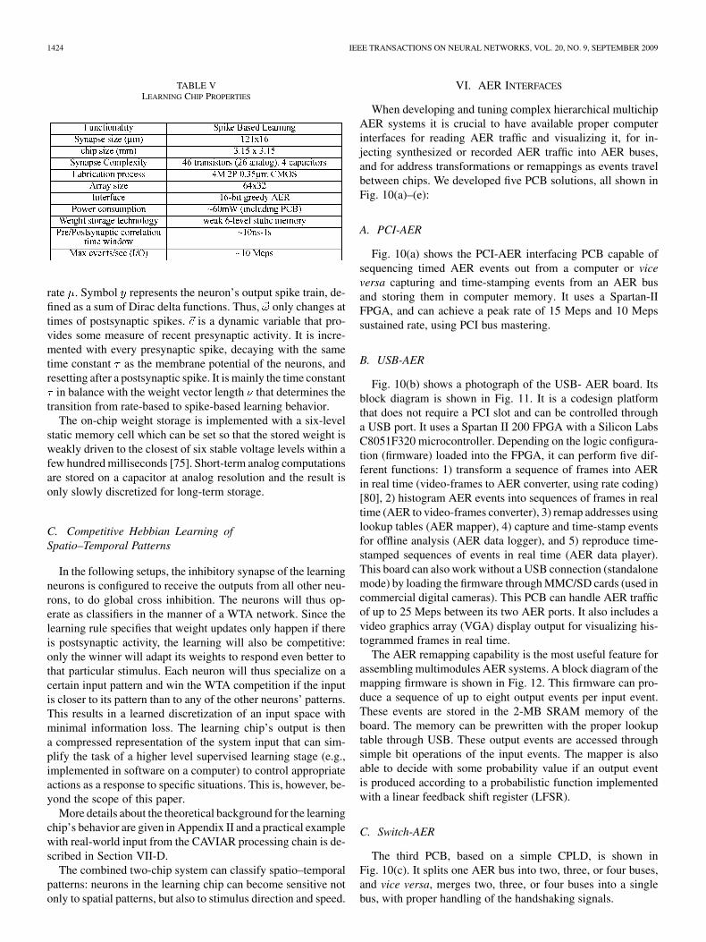
1424 IEEE TRANSACTIONS ON NEURAL NETWORKS, VOL. 20, NO. 9, SEPTEMBER 2009
TABLE VLEARNING CHIP PROPERTIES
rate . Symbol represents the neuron’s output spike train, de-fined as a sum of Dirac delta functions. Thus, only changes attimes of postsynaptic spikes. is a dynamic variable that pro-vides some measure of recent presynaptic activity. It is incre-mented with every presynaptic spike, decaying with the sametime constant as the membrane potential of the neurons, andresetting after a postsynaptic spike. It is mainly the time constant
in balance with the weight vector length that determines thetransition from rate-based to spike-based learning behavior.
The on-chip weight storage is implemented with a six-levelstatic memory cell which can be set so that the stored weight isweakly driven to the closest of six stable voltage levels within afew hundred milliseconds [75]. Short-term analog computationsare stored on a capacitor at analog resolution and the result isonly slowly discretized for long-term storage.
C. Competitive Hebbian Learning ofSpatio–Temporal Patterns
In the following setups, the inhibitory synapse of the learningneurons is configured to receive the outputs from all other neu-rons, to do global cross inhibition. The neurons will thus op-erate as classifiers in the manner of a WTA network. Since thelearning rule specifies that weight updates only happen if thereis postsynaptic activity, the learning will also be competitive:only the winner will adapt its weights to respond even better tothat particular stimulus. Each neuron will thus specialize on acertain input pattern and win the WTA competition if the inputis closer to its pattern than to any of the other neurons’ patterns.This results in a learned discretization of an input space withminimal information loss. The learning chip’s output is thena compressed representation of the system input that can sim-plify the task of a higher level supervised learning stage (e.g.,implemented in software on a computer) to control appropriateactions as a response to specific situations. This is, however, be-yond the scope of this paper.
More details about the theoretical background for the learningchip’s behavior are given in Appendix II and a practical examplewith real-world input from the CAVIAR processing chain is de-scribed in Section VII-D.
The combined two-chip system can classify spatio–temporalpatterns: neurons in the learning chip can become sensitive notonly to spatial patterns, but also to stimulus direction and speed.
VI. AER INTERFACES
When developing and tuning complex hierarchical multichipAER systems it is crucial to have available proper computerinterfaces for reading AER traffic and visualizing it, for in-jecting synthesized or recorded AER traffic into AER buses,and for address transformations or remappings as events travelbetween chips. We developed five PCB solutions, all shown inFig. 10(a)–(e):
A. PCI-AER
Fig. 10(a) shows the PCI-AER interfacing PCB capable ofsequencing timed AER events out from a computer or viceversa capturing and time-stamping events from an AER busand storing them in computer memory. It uses a Spartan-IIFPGA, and can achieve a peak rate of 15 Meps and 10 Mepssustained rate, using PCI bus mastering.
B. USB-AER
Fig. 10(b) shows a photograph of the USB- AER board. Itsblock diagram is shown in Fig. 11. It is a codesign platformthat does not require a PCI slot and can be controlled througha USB port. It uses a Spartan II 200 FPGA with a Silicon LabsC8051F320 microcontroller. Depending on the logic configura-tion (firmware) loaded into the FPGA, it can perform five dif-ferent functions: 1) transform a sequence of frames into AERin real time (video-frames to AER converter, using rate coding)[80], 2) histogram AER events into sequences of frames in realtime (AER to video-frames converter), 3) remap addresses usinglookup tables (AER mapper), 4) capture and time-stamp eventsfor offline analysis (AER data logger), and 5) reproduce time-stamped sequences of events in real time (AER data player).This board can also work without a USB connection (standalonemode) by loading the firmware through MMC/SD cards (used incommercial digital cameras). This PCB can handle AER trafficof up to 25 Meps between its two AER ports. It also includes avideo graphics array (VGA) display output for visualizing his-togrammed frames in real time.
The AER remapping capability is the most useful feature forassembling multimodules AER systems. A block diagram of themapping firmware is shown in Fig. 12. This firmware can pro-duce a sequence of up to eight output events per input event.These events are stored in the 2-MB SRAM memory of theboard. The memory can be prewritten with the proper lookuptable through USB. These output events are accessed throughsimple bit operations of the input events. The mapper is alsoable to decide with some probability value if an output eventis produced according to a probabilistic function implementedwith a linear feedback shift register (LFSR).
C. Switch-AER
The third PCB, based on a simple CPLD, is shown inFig. 10(c). It splits one AER bus into two, three, or four buses,and vice versa, merges two, three, or four buses into a singlebus, with proper handling of the handshaking signals.
SERRANO-GOTARREDONA et al.: CAVIAR: A 45K NEURON, 5M SYNAPSE, 12G CONNECTS/S AER HARDWARE 1425
Fig. 11. USB-AER codesign PCB block diagram. A Silicon Labs C8051F320USB microcontroller with SD/MMC support, connected with a Xilinx Spartan2 FPGA. The FPGA firmware is able to perform complex operations with thetwo AER buses, the SRAM memory, and the VGA interface.
D. Mini-USB-AER
Fig. 10(d) is a lower performance but more compact bus-pow-ered USB interface based on a C8051F320 microcontroller. Itcaptures and time-stamps events to a computer at peak ratesof up to 100 kilo events per second (keps) and is particularlyuseful for portable demonstrations, and the components cost isless than $20 [22].
Fig. 12. Mapper block diagram: through the USB, the mapping table is storedin the external SRAM memory and per each input event the control unit (CU)generates the sequence of up to eight probabilistic output events.
E. USB2AER
The last board, shown in Fig. 10(e), is a bus-powered USBversion of the PCI-AER board. This board supports USB 2.0high speed, allowing event rates of 6 Meps between the com-puter and the AER chip both for sequencing and for monitoringpurposes [64].
The next section describes the operation of the CAVIARdemonstrator system, shown in Fig. 13 where we made exten-sive use of the AER interfacing PCBs. The USB-AER boardremapped AEs in real time. The USB2AER board is used as anAER monitor (to visualize reconstructed/histogrammed imagesin real time) and for storing time-stamped events in computermemory for offline analysis.
1426 IEEE TRANSACTIONS ON NEURAL NETWORKS, VOL. 20, NO. 9, SEPTEMBER 2009
Fig. 13. Experimental setup of multilayered AER vision system for ball tracking (final demonstrator of CAVIAR FET project). (a) Block diagram (white boxesinclude custom designed chips and gray boxes are interfacing PCBs). (b) Photograph of a setup.
The reconfigurability of the boards was actively used duringthe CAVIAR project developments to test, debug, and adjusteach layer of the processing separately, or two by two. Forexample, a repetitive input sequence of events is useful forproper tuning of biases and kernels for testing the convolutionchips. For this, one can use the USBAER board (with AERdata logger firmware) to capture a time-stamped sequence ofevents from the retina to a file. One can later reconfigure theboard to act as an input to the convolution chip by repeatedlyreproducing these stored events in real time (by loading theAER data-player firmware for this functionality). Often, duringthe CAVIAR project development, events were recorded in onelab and reproduced at a different lab. This way one partnercould use the output of a previous block as their input withouthaving this block physically present in their lab [62], [80].
VII. THE CAVIAR VISION SYSTEM
Using all these building blocks, we assembled the frame-free spike-based sensing–processing–actuating–learning AERvision system shown in Fig. 13. A mechanical rotor (1) holdsa rotating white piece of paper with two circles of different ra-dius and some distracting geometric figures. The vision systemfollows the two circles only, and discriminates between the two.A pair of servomotor driven mirrors changes the point of viewof the AER retina (3), which sends outputs to a monitor PCB(4), and a mapper PCB (5) before reaching the convolution PCBwith four convolution chips (6). The latter PCB output is sentthrough another monitor PCB (7) and mapper PCB (8) to the2-D WTA “object” chip (9). This output is received by a monitorPCB (10) which sends a copy to a microcontroller (11) that con-trols the mirror motors (2) to center the detected circle. Another
SERRANO-GOTARREDONA et al.: CAVIAR: A 45K NEURON, 5M SYNAPSE, 12G CONNECTS/S AER HARDWARE 1427
copy of the WTA output is sent to the learning system whichconsists of a mapper (12), a delay line chip (13), another mapper(14), and a learning classifier chip (15), and which learns to clas-sify trajectories into different classes.
The temporal contrast retina provides an output event spaceof size 128 128 pixels. The four-convolution-chip PCB canprocess the complete 128 128 retina space, although it wouldcompute the convolution output for only the central 64 64pixels. In our setup, we introduced a mapper between theretina PCB and convolution PCB (block 5 in Fig. 13) todownsample from 128 128 pixels to 64 64 pixels. Thisway, the convolution PCB will provide outputs for the completeretina visual range. The mapper also eliminates the retina sign bit,since the convolution stage needs to detect full circumferences.In the following experiments, we used circular kernels such asthe ones in Fig. 3(c) and (d), which emphasize circumferencesof particular sizes by doing template matching. Using thesekernels continuously is somehow similar to performing circularHough transforms [65], which detect the locations of circularfeatures in the input, except that we use analog graded valuesand include negative kernel values for penalizing the absenceof features.
The 64 64 convolution output is fed through a mapper thatsubsamples to a 32 32 space for the WTA (object) chip. ThisWTA output provides cleaned up coordinates for the center ofthe target-size detected circle. This signal is split at this pointinto two separate paths: (a) the motor control subsystem and (b)the learning subsystem.
The motor control subsystem is built using a commercial mi-crocontroller which acts on two servomotors, each holding onemirror. One of the mirrors is tilted horizontally while controlledby the -coordinate of the “object” chip output, and the othermirror is tilted vertically while controlled by the - coordinateof the “object” chip output. This way, the coordinate providedby the “object” chip represents the deviation of thedetected circle from center of the field of view. A proportionalcontroller (11 in Fig. 13) uses the motor system to zero this error,thus keeping the target-size circle centered on the field of viewof the WTA.
The object centering can be seen in Fig. 14. The threesubfigures show the outputs captured by the three monitorPCBs in Fig. 13, when the feedback servo control is enabledto center the detected object. Monitor PCBs connect to a hostcomputer through a high-speed USB2.0 connection, sendingAEs at a speed of up to a peak rate of 6 Meps. The jAERsoftware [22] reads those events, and reconstructs and renders2-D histograms by collecting events belonging to a time slicewhich is programmable. If this time slice is similar to themonitor refresh rate, one can visualize the reconstructed images(video) in real time. For high-speed phenomena, one canconfigure a time slice of very short duration (down to a fewmicroseconds) and visualize a slow-motion recorded sequenceof events offline.
Fig. 14(a) shows a histogram reconstructed from the128 128 retina output captured by monitor PCB (4) inFig. 13. White dots represent positive sign events (dark-to-lighttransitions) and black dots negative sign events (light-to-darktransitions), allowing identification of the direction of motion
Fig. 14. The 20-ms snapshot of outputs of vision tracking system. The retinacentral point of view is changed dynamically to follow the small circle, whichappears always centered in the field of view.
Fig. 15. Electronic centering. (a) Raw retina output over 1.3 s without cen-tering. (b) With electronic centering using WTA to steer retina output.
of the geometric figures, which is clockwise in this case.Fig. 14(b) also shows a histogram image reconstructed from the64 64 convolution PCB output captured by monitor PCB (7)in Fig. 13. In this case, the kernel was programmed to detect thesmall circle [see Fig. 3(c)]. Positive sign events (white) showwhere the small circle is centered, while the negative events(dark) show where it is not. The convolution output includessome noise, which is filtered out by the WTA operation. Theconvolution output pixels are transformed from size 64 64to 32 32 (by grouping 2 2 pixels into one) by the mapper(8) in Fig. 13. Fig. 14(c) also shows the output of the WTAcomputing stage, where all noise has been filtered out. Thedark pixels are the local and global inhibitory units for eachquadrant.
We also implemented a fully electronic (without mirrors, me-chanical parts, or motors) servo system for changing the centralview point. For this system, an extra splitter was inserted at theretina output. The extra retina output together with the WTAoutput were fed to an extra mapper, subtracting. The result isthe same as when using the mirrors, except that now the max-imum rotating speed of the stimulus is not limited by the timingconstraints of the mechanical components and the object mustremain in the field of view of the fixed retina. Fig. 15(a) showsthe accumulated retina output over 1.3 s without centering andall three objects rotate around the center of view. Fig. 15(b)shows the electronically centered retina output. Now the dis-tractor objects rotate around the centered large circle, which wasprogrammed into the convolution chip kernels.
1428 IEEE TRANSACTIONS ON NEURAL NETWORKS, VOL. 20, NO. 9, SEPTEMBER 2009
Fig. 16. A 3-D �-� time reconstruction of events captured during a 100-msinterval with a rotating stimulus of two circles of different radii, rotating at fourrevolutions per second. Events are captured from the retina output (small dots),from the convolution PCB output (circles), and from the WTA output (big stars).
A. The 3-D Reconstruction of Captured Events
For precise timing measurements, we need to visualize cap-tured events as function of time. To illustrate this, we performedthe same experiment as discussed in Figs. 13 and 14, but thistime using a stimulus with two circles rotating at four revolu-tions per second and disconnecting the feedback servo mecha-nism to center one of the circles. Fig. 16 shows the events cap-tured during a 100-ms time interval, from the retina, convolutionchip, and object chip. This data shows how the retina output isfiltered down by the convolution to a cloud mostly around thecenter of the matching input circle, and how the WTA events fur-ther reduce the data to just events centered on the programmedobject.
B. Spike Output Statistics
From the recorded time-stamped spike information, we canperform various analysis, for example, measuring the exact sta-tistical distribution of the outputs from the different chips. Thismeasured distribution is useful when setting up the parametersof a chip to process its inputs. For example, since the task ofWTA chip in the CAVIAR system during the visual trackingtask is to localize the optimal location of the desired stimulus,the known statistical distribution of its inputs helps in the properconfiguration of the parameters of the WTA chip [67]. The sta-tistics of these spikes are important because the WTA is the firstnonlinear decision making module in the CAVIAR chain. Todetermine the actual statistics of the convolution chip, we an-alyzed its output spike data in response to a disc rotating withconstant velocity in front of the retina (Fig. 16). The convolu-tion chip contains a matched-filter kernel of one size of a circle.The output spikes from the convolution chip in this figure indi-cate the location of the center of the detected kernel in the fieldof view. To simplify the subsequent analysis, we transformedthe 2-D convolution chip output into 1-D by considering onlyneurons along the stimulus trajectory [Fig. 17(b)]. This trans-formation is possible since we know the trajectory in this simpleproblem. The transformation discards activity from neurons out-side the trajectory of the stimulus center. These outliers receiveless input than neurons on the trajectory and do not evoke output
Fig. 17. Spatial trajectory of the stimulus center. The stimulus is a disc thatrotates with constant velocity in front of the retina. (a) The convolution stagecontains a matched-filter kernel; its output is a smoothed version of the center ofthe object. The gray level gives the spike count for one revolution of the stimulus.(b) For the analysis, we consider only pixels that fall onto the trajectory of thestimulus. We masked these pixels with a manually defined region of interest.
Fig. 18. Raster plot of the input spike trains from the convolution chips tothe WTA chip. Input addresses along the trajectory are sorted in the order ofthe stimulus movement. Each point marks one spike (every spike train containsabout 20–40 spikes). Data from one revolution of the stimulus disc are shown.
spikes from the WTA. Our analysis focuses on the spatio–tem-poral estimation of the stimulus position, for which only the neu-rons with a significant spike input are relevant.
Fig. 18 shows the input spike trains to the WTA neurons alongthe stimulus trajectory before alignment, but sorted by theirmean spike time. From this representation, the average travel-ling time from one neuron to the next can be calculated, byaveraging the difference in the mean time between each pair ofneighboring input channels. By using a time-rescaling methodto convert the nonstationary output of the convolution chip to astationary one, subsequent analysis of the homogeneous distri-bution shows that the outputs are well modeled by a travellingGaussian wave with Poisson statistics [67], [68], [90].
1) Reconstruction of Object Position From WTA: We con-sider how well the WTA network can reconstruct the stimulusposition by requiring each output spike of the WTA to indicatethe actual object position. The object position is discretized invalue to the neuron address and in time to the occurrence of theoutput spikes as quantized by the recorded time stamp.
SERRANO-GOTARREDONA et al.: CAVIAR: A 45K NEURON, 5M SYNAPSE, 12G CONNECTS/S AER HARDWARE 1429
Fig. 19. Reconstruction of object position from the WTA output spikes. Hor-izontal axis is time (units in seconds) and vertical axis is neuron number (withunits in pixels).
Fig. 20. Events obtained with a circle of flashing LEDs. (a) The 3-D �-� timereconstruction of events from the retina, convolution PCB output, and WTAoutput, captured during 200 ms. LEDs were flashing with an 80-ms period. (b)� time projection of one of the transients.
Fig. 19 shows how we can reconstruct the stimulus positionfrom this asynchronous representation. The ideal output of thenetwork is an update of the object position as soon as the objectis aligned to a new neuron (dashed staircase). Since the object inour experiment moves with constant speed, the transition timefrom each neuron to the next is constant. In the sparsest rep-resentation, the network would elicit one spike at each verticalline of the dashed staircase function. In the CAVIAR data (con-tinuous staircase), the WTA network elicits more spikes thanone spike per position, as illustrated by the output spike trainof the network at the top of Fig. 19. This leads to switching inthe predicted object position, for example, between neurons 17and 18. In addition, the output sometimes indicates an incorrectposition, for example, at neurons 18 and 19, or the spike timesare jittered, for example, at neurons 13 and 14.
We determine how much the object position reconstructedfrom the output spikes of the WTA network deviates from theideal case in both position and time. We call an error in the ob-ject position a “classification error” if a neuron other than the
Fig. 21. Raster plot and cycle histogram of the activity of all 32 neurons afterrandom initialization of the weights with learning turned off. Cycle times areindicated by the vertical dotted lines. Two neurons (9 and 20) are very dominantand mostly active for more than one cycle. This is a bad representation of thestimulus that will not allow to determine the stimulus’ position within a cycle.
one aligned to the object position makes an output spike. Thiserror is derived from a probability distribution. The spike timeof the neuron before or after the ideal point in time is consid-ered as jitter. This error is normalized by the average timetaken by the ball to proceed between one neuron to the next.For example, in Fig. 19, 1.2 s/17. Both errors are inducedby the Poisson statistics of the input and the variations in itsparameters. Since both jitter and classification error are interde-pendent, we use an error measure , which quantifies the pixelerror, and is computed as the area difference between the re-constructed object location (dashed staircase) and the ideal case(continuous staircase), normalized to times the number ofneurons (pixels) . The error from this experimental set ob-tained for one ball velocity is
(2)
which indicates an average error position of slightly better thana single pixel if one looks at the decision of the network at anyone moment in time. This accuracy is achieved because the av-erage WTA spike location, combined with its precision timing,overcomes the quantization and other noise sources.
C. Latency Measurements
To measure the chain processing latency, we stimulated thesystem with a circle of flashing light-emitting diodes (LEDs).The size of the flashing circumference is equal to one of thekernel sizes in the convolution chips. The LEDs are turned onand off with a period of 80 ms, and events are captured fromthe same three nodes as in Section VII-A. Fig. 20(a) shows theevents captured from these three nodes during a time slice of200 ms. We see event bursts every 40 ms, which corresponds toeither a transient OFF–ON or ON–OFF of the diodes (here we areignoring the sign bit of the retina). Fig. 20(b) shows the -timeprojection of one such burst. We can see that the transient outputof the retina lasts around 2 ms (the most dense part). The con-volution output events start to appear between 0.5 and 1.0 msafter the initial wavefront of the retina (it needs enough events
1430 IEEE TRANSACTIONS ON NEURAL NETWORKS, VOL. 20, NO. 9, SEPTEMBER 2009
to recognize the circle). The WTA stage fires an event with adelay of around 3 ms with respect to the onset of the convolu-tion output. Not every convolution output burst produces a WTAoutput event [Fig. 20(a)]. In this configuration, the WTA was bi-ased to produce a reduced number of events (without spuriousor noisy events), so that in the experiment of Figs. 13 and 14,the mechanical stimulus centering section would receive a cleancontrol signal with as little noise as possible.
D. Learning in the CAVIAR Demonstrator
In this section, we demonstrate the performance of theCAVIAR learning chips in achieving unsupervised classi-fication of phases in a cyclic trajectory [73]. Thus, a com-pressed/quantized representation of that trajectory is learned,minimizing information loss.
The spatio–temporal learning classifier was connected to theWTA stage while the processing chain was configured to trackthe larger of two rotating circles. A sequence of the input to thelearning system is depicted in Fig. 16 as a 3-D scatter plot. Thisinput is projected (downsampled) to 2 2 pixels by combiningall events from one quadrant into a single event stream. Thisis a low resolution and without the temporal aspect one couldonly hope to classify the WTA output into four categories, sincethere are now only four positions in space. However, these 2 2spike trains are inserted into the delay line chip that is config-ured correspondingly as four separate delay lines (56 320 delayelements each). Those delay lines are tapped at three differentdelays (approximately 0 s, 200 ms, and 400 ms) and the resulting2 2 3 spike trains are passed on to the learning chip. Thereis now significantly more information that can be categorizedby the learning chip: for example, different speeds and direc-tions and in our case a higher spatial resolution, as the stimuluswill cause several different trajectory patterns as it crosses be-tween spatial pixels. The learning chip has been tuned to expressrate-based learning behavior with an approximate time constantof 200 ms. The task of the learning classifier chip is now to pro-vide a good representation of at most 32 categories (since thereare 32 neurons) from the repeated spatio–temporal pattern.
After random initialization of the weights, the learning clas-sifier performs poorly, as expected (Fig. 21). The cyclic motion(the vertical dotted lines represent the cycle frequency) cannoteasily be deduced from the active neuron outputs: individualneurons remain exclusively active over several stimulus cyclesand the activity is dominated by two to three neurons. Thesewere often the same neurons in different experiments, since theytend to have generally stronger synapses due to transistor mis-match.
After learning for a few cycles, the situation is improved(Fig. 22). More neurons (approximately seven to nine) show sig-nificant activity and they are clearly phase locked with the stim-ulus. They have become specialized on a spatio–temporal inputpattern that occurs during the cyclic object trajectory. They pro-vide a richer encoding of the cyclic pattern, representing severaldifferent phases of the motion. Effects of device mismatch thatput some neurons at an initial disadvantage are, thus, partiallycountered by learning, although still only 9 of 32 total neuronsshow significant activity with these parameter settings. Consid-ering that there are still only four positions to distinguish (after
Fig. 22. Neuron activity after learning. The activities of several neurons arereliably phase locked at different phase delays and allow stimulus reconstructionwith a better resolution than the cycle time.
the input space projection) and that the object only moves in onedirection at constant speed, this is in fact a rather good perfor-mance. One could have expected that there are still only four dif-ferent input patterns and that maximally four neurons could spe-cialize on exactly those four patterns, but since this real-worldinput is changing its state in a continuous fashion rather than justassuming four discrete states, some of the neurons have becomeselective for transitory states “between” the four positions.
A more quantitative analysis [73] with three test sets of dif-ferent well-controlled simulated inputs instead of real sensordata has shown that the chip implementation of the learning al-gorithm is able to improve information content of the network’soutput by 16%–20%, always close to the theoretical optimumfor these particular test cases.
VIII. CONCLUSION AND FUTURE OUTLOOK
This paper demonstrates the high potential of modular AERhardware systems. To illustrate this, it demonstrates a multichipmultilayer vision sensing processing and actuating architecture,configured for fast recognition and tracking of moving circles.
What is unique about the example system presented here isthat it is composed of multistages of AER processing modulesinterconnected through multiple independent AER links, mim-icking the multilayer structure of neural cortex. This approachallows to feasibly scale up systems by either adding more par-allel modules in a layer, adding more layers, or even includingrecurrent feedback connections.
The CAVIAR system consists of about 45k spiking neuronsand 5M synapses; and it can perform up to 12G connec-tions/operations per second.2 These metrics are computed asfollows. For processing one 31 31 kernel the convolutionchips need 330 ns per input event. Since there are four chips inparallel, it yields (4 31 31/330 n ) operations/s. The
2Here “connections/s” represents the traditional neural network (hardwareand software) computational performance figure describing the number ofsynaptic connections computed per unit time. Note that this is not equal tothe number of physical events communicated through an AER channel. Ourconvolution chips are very efficient in this sense, because for each input event,they can process up to ��� �� � ��� synaptic connections in 330 ns � �����
connections/s/chip.
SERRANO-GOTARREDONA et al.: CAVIAR: A 45K NEURON, 5M SYNAPSE, 12G CONNECTS/S AER HARDWARE 1431
synaptic strengths are 5-b values. For communicating analogvalues, one needs several events (assuming rate coding) forthe same synapse between neurons A and B. Therefore, thisfigure could also be regarded as representing 12 giga eventsper second (Geps). Regarding the 5M synapses, what mattersare the possible connections the system can be configuredto implement. Of course, since this is implemented throughconvolutions, the projection fields have the restriction that theyare position independent. The possible synaptic connectionsare as follows. From the retina to the convolution chip, thereare up to 3.94M possible con-nections and from the convolution chip to the WTA there are
1.05M connections, resulting in a totalof approximately 5.2M synapses, but using 6.1k unique valuedsynapses. All these figures (number of neurons, synapses, andeps or connections/s) would scale up linearly by adding moremodules to the system. This is because our up-scaling approachconsists of adding AER modules as well as independent AERchannels [91]. The ultimate bottleneck is the throughput of anindividual AER channel. Splitting AER channels replicatestheir traffic while reaching more modules. On the other hand,merging AER channels increases throughput on the resultingchannel. To avoid channel saturation, this merging should bedone with some care (for example, instead of merging 100channels and perform a convolution, one can merge them ingroups of ten, do the same convolution with ten independentmodules, and merge the ten convolution outputs).
The CAVIAR system in its present form has drawbacks. Themajor ones are the complexity of the hardware setup and the lackof rapidly configured flexibility. The present components sharea common communication infrastructure and standardized ca-bling and logic protocols, but not a common configuration in-frastructure. Each partner had developed their own tools andhardware and software interfaces for configuring chip biases,address mappings, and calibration, leading to the requirementfor at least two experienced operators for the setup of the systemand the use of typically two computers to impose the desiredconfiguration over USB interfaces. The learning capabilities ofCAVIAR are limited by the small numbers of plastic synapses.In addition, a major unsolved problem in computer science isthe lack of general understanding of how to impose a desiredbehavior on interconnected networks of simple computing ele-ments or how learning should be incorporated efficiently intothe system. Thus, it is difficult to encode known mathemat-ical signal processing methods or branch-like behavior whichcan readily be serially programmed but not configured into thesystem’s connectivity.
Spinoff activities from this CAVIAR project are the ongoingdevelopment of fully digital convolution chips [86], applicationin real-time robotics [87] and commercialization [88] of the sil-icon retina, development of tools for behavioral simulation offuture AER systems [89], and the active open-source softwareproject jAER for real-time event-based procedural processingof AER sensor data [22], [90].
Still, this real-time hardware implementation of a neurophys-iological model is far from attaining the same complexity as thatof any brain: it consists of about six orders of magnitude fewerneurons and about eight orders fewer synapses than a human
brain. It requires slightly more space than a shoe box. Thus, if wewould hypothetically scale it up to synapses, the 100 mil-lion shoe boxes would easily fill a few good sized warehouses.
Nevertheless, this AER system is a significant step towardsthe construction of more complex real-time, and real-worldinteractive artificial neural systems. We plan to miniaturizeit by about 3–4 orders of magnitude within the next fewyears, by increasing the numbers of synapses and neurons perAER-module and by integrating more modules into a smallerphysical volume. With present day miniature surface mountPCB technology and the latest deep submicron complementarymetal–oxide–semiconductor (CMOS) technology, it is quiterealistic to fit about 100 chips of 256 256 neurons each,with 32 32 synapses per neuron. One such PCB would host6.5 10 neurons and 6.7 10 synapses. Assuming timing de-lays similar to those reported in this paper, preliminary results[91] suggest that these systems could perform sophisticatedobject recognition with delays around 100 s. This wouldbe equivalent to a computing power of 100 chips 6.7 10synapses/chip/100 s 6.7 10 MAC/s (multiply and accu-mulates per second), which is 3–4 orders of magnitude abovepresent state-of-the-art dedicated hardware for high-speedvision processing (see Appendix I).
With such developments, we will be able to provide a modularand scalable platform for real-time implementations of neuralmodels of a really challenging complexity. Coupling this mas-sive preprocessing power with flexible back-ends of conven-tional procedural computation will enable solutions to a host ofpractical applications.
APPENDIX ICOMPARISON TO CONVENTIONAL FRAME-BASED IMAGE
PROCESSING APPROACHES
Other approaches to image processing are based on aframe-by-frame acquisition and consequent processing. Letus distinguish between the sensing step (acquiring an imageframe) and the processing steps (processing the sequences offrames).
A. Sensing Step
Frames are acquired at a given frame rate , and each pixelintegrates light during a time period . Usually both times aresimilar, although the latter has to be at least slightly smaller. Forhigh-speed images, one can increase frame rate (which rendersan explosion in the number of frames to process afterwards), orreduce to avoid blurring of fast moving objects (which re-duces either exposure times or image quality, or results in moreexpensive imagers). If one chooses to reduce while keepingframe rate constant , then there will be informa-tion missing for a time . This can be a severe limitationfor recognition/tracking of moving objects. On the other hand,if one keeps , either is too small yielding an exces-sive number of frames for processing or is too large, yieldingblurred images. In any case, a compromise has to be reached,and, in either case, one always suffers the physical restriction ofintegrating light during a finite time period , thus averaginglight over this time.
1432 IEEE TRANSACTIONS ON NEURAL NETWORKS, VOL. 20, NO. 9, SEPTEMBER 2009
For the sensors in this paper and related work, things are dif-ferent. Each pixel has an internal light-dependent photocurrentwhich is continuous in time. In a luminance retina, it is directlycoded into event frequency [38]. In a spatial [23] or temporalcontrast [20] retina, its derivative is computed continuously andcoded as pixel events. Consequently, as soon as a contrast is de-tected, events are sent out with very short delays: pixels do notwait for their frame rate refresh instant. This way, the precisetiming of what is happening in the real world is preserved withAER frameless vision sensors. This allows to sense visual re-ality with timings equivalent to conventional cameras acquiring10 000 frames/s or faster. The retinas developed in the contextof the CAVIAR project are low power ( 10 mW), small area( 5 mm ), standard CMOS low-cost chips, as opposed to theirhigh-end counterpart of imagers capable of operating at 10Kframes/s.
B. Processing Steps
There are a number of solutions and products in the marketfor performing sophisticated visual object recognition tasks.All of them are based on sequential frame acquisition, andconsequently suffer from the limitations mentioned above.Assuming images are acquired with satisfactory quality forlater processing, let us now compare the CAVIAR approachto other conventional approaches, from the processing pointof view. In the conventional approach, the usual solutionis to perform the high-computation demanding operations(such as 2-D convolutions) on high-speed DSPs (for example,TMS320DM6446 DaVinci from Texas Instruments, specialfor video applications) or using computers with fast centralprocessing units (CPUs) and special multimedia-orientedinstructions. DSP TMS320DM6446 [92] can optimisticallyprocess up to 2.4 10 MAC/s (multiply accumulates persecond). This will allow to perform a generic (no symme-tries) 16 16 kernel convolution on a 256 256 image in 7ms ( 143 convolutions/s). Other more vision-oriented DSPchips, such as the DaVinci TMS320DM355 [93], are howeverdesigned for standard consumer video cameras operations likeMPEG compression/decompression, histogramming, resizing,and autofocus. They do not implement 2-D convolutions di-rectly, and are not really meant for recognition tasks.
Perhaps the most impressive chip available presently is theMathStar3 field-programmable object array (FPOA): for ex-ample, it can process large kernel (16 16, although they musthave symmetry constraints) 2-D convolutions on 256 256images at a rate of 100 convolutions/frame at 25 frames/s( 2500 convolutions/s). This is equivalent to 3.8 10MAC/s. However (and ignoring the restriction on kernel sym-metry), this approach is not scalable to multiple chips whilemaintaining speed.
C. Software Solutions
Commercial computers rely on video graphic cards for per-forming efficiently vision recognition convolution-based-likealgorithms. Such cards ultimately use special purpose chipslike those discussed above. At present, graphics processing unit
3www.mathstar.com
(GPU) chips are very popular among these cards. Cope et al.[95] perform a comparison of software using GPU versus CPUfor 2-D convolutions. Performance changes with kernel size.The equivalent MAC per second can be obtained from [95] bymultiplying the pixel throughput (number of pixels processedper second) by the number of MAC per pixel (which varies from4 for a 2 2 kernel convolution to 121 for an 11 11 one): astate-of-the-art GPU yields 4 10 MAC/s for 2 2 kernelsand 7.3 10 MAC/s for 11 11 kernels, while a Pentium 4 at3 GHz ranges from 6 10 MAC/s for 2 2 kernels to 1.210 MAC/s for 11 11 kernels.
APPENDIX IICOMPETITIVE HEBBIAN LEARNING FOR CLASSIFICATION
Weight vector normalizing competitive Hebbian learning hasbeen used to achieve principal component analysis (PCA) [76].One particular implementation of this is Sanger’s rule [77]. Itdiffers somewhat from the implementation presented here: sinceSanger’s rule implements the inhibitory term into the learningrule, whereas here the neurons’ activities inhibit each other andthus, indirectly the learning term. Furthermore Sanger’s ruleachieves ordered PCA because it only introduces partial crossinhibition, where “higher order neurons” inhibit “lower orderneurons” but not vice versa. Here full cross inhibition, whichhas also been suggested, for example, in [78], would lead to un-ordered extraction of principle components.
The experiments here, however, are set up such that not allconditions for computing a PCA are met. The input distributionis not of zero mean, weights and signals can only be positive,and the cross-inhibition is so strong as to induce “hard” WTA,where all neurons but the winner are suppressed completely andthe number of neurons is bigger than the dimensionality of theinput space. So how can the resulting behavior be described?
Integrate-and-fire neurons described in terms of signal ratesbehave like linear threshold elements [73]
if
if(3)
where is the neuron’s weight vector, is the input vector, isthe output, is the time constant of the leakage, and is the an-gular distance between and . This shows that with the weightvector normalized to the same length for all neurons, the neuronwith the smallest will always win the WTA competition andthus the input space is carved up into different classes along hy-perplanes of equal angular distance between the weight vectors.
Hebbian learning will reduce the angular distance betweenthe input vector and . Thus, the winning neuron will adapt its
closer to . With no competitors and the inputs limited to thefirst hyperoctant (only positive input vector elements) a neuronwill tend to move towards the direction of the most dense distri-bution of long input vectors. When competing with others, it willmove towards dense regions of inputs that are not yet claimedby another neuron. This behavior is much akin the well-knownlearning vector quantization (LVQ) algorithm [94], with the dif-ference that the weight vectors move according to their angulardistance to the inputs, not their Euclidian distance, and that the
SERRANO-GOTARREDONA et al.: CAVIAR: A 45K NEURON, 5M SYNAPSE, 12G CONNECTS/S AER HARDWARE 1433
Fig. 23. Example for learning classification with weight vector normalizingcompetitive Hebbian learning.
input space is separated along hyperplanes of equal angular dis-tance between weight vectors, and not equal Euclidian distance.
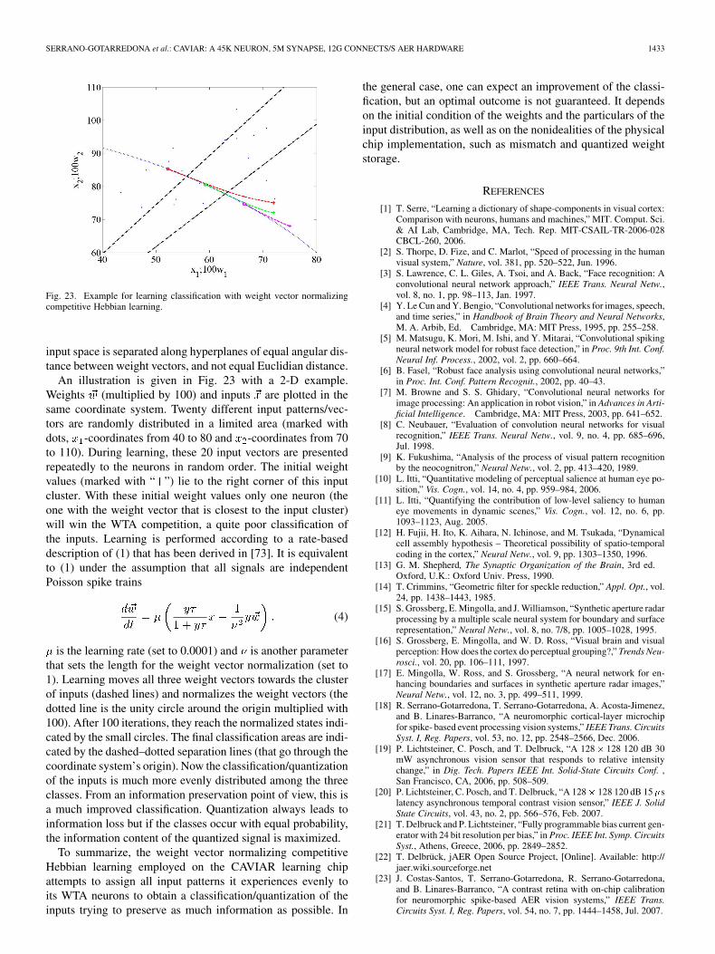
An illustration is given in Fig. 23 with a 2-D example.Weights (multiplied by 100) and inputs are plotted in thesame coordinate system. Twenty different input patterns/vec-tors are randomly distributed in a limited area (marked withdots, -coordinates from 40 to 80 and -coordinates from 70to 110). During learning, these 20 input vectors are presentedrepeatedly to the neurons in random order. The initial weightvalues (marked with “ ”) lie to the right corner of this inputcluster. With these initial weight values only one neuron (theone with the weight vector that is closest to the input cluster)will win the WTA competition, a quite poor classification ofthe inputs. Learning is performed according to a rate-baseddescription of (1) that has been derived in [73]. It is equivalentto (1) under the assumption that all signals are independentPoisson spike trains
(4)
is the learning rate (set to 0.0001) and is another parameterthat sets the length for the weight vector normalization (set to1). Learning moves all three weight vectors towards the clusterof inputs (dashed lines) and normalizes the weight vectors (thedotted line is the unity circle around the origin multiplied with100). After 100 iterations, they reach the normalized states indi-cated by the small circles. The final classification areas are indi-cated by the dashed–dotted separation lines (that go through thecoordinate system’s origin). Now the classification/quantizationof the inputs is much more evenly distributed among the threeclasses. From an information preservation point of view, this isa much improved classification. Quantization always leads toinformation loss but if the classes occur with equal probability,the information content of the quantized signal is maximized.
To summarize, the weight vector normalizing competitiveHebbian learning employed on the CAVIAR learning chipattempts to assign all input patterns it experiences evenly toits WTA neurons to obtain a classification/quantization of theinputs trying to preserve as much information as possible. In
the general case, one can expect an improvement of the classi-fication, but an optimal outcome is not guaranteed. It dependson the initial condition of the weights and the particulars of theinput distribution, as well as on the nonidealities of the physicalchip implementation, such as mismatch and quantized weightstorage.
REFERENCES
[1] T. Serre, “Learning a dictionary of shape-components in visual cortex:Comparison with neurons, humans and machines,” MIT. Comput. Sci.& AI Lab, Cambridge, MA, Tech. Rep. MIT-CSAIL-TR-2006-028CBCL-260, 2006.
[2] S. Thorpe, D. Fize, and C. Marlot, “Speed of processing in the humanvisual system,” Nature, vol. 381, pp. 520–522, Jun. 1996.
[3] S. Lawrence, C. L. Giles, A. Tsoi, and A. Back, “Face recognition: Aconvolutional neural network approach,” IEEE Trans. Neural Netw.,vol. 8, no. 1, pp. 98–113, Jan. 1997.
[4] Y. Le Cun and Y. Bengio, “Convolutional networks for images, speech,and time series,” in Handbook of Brain Theory and Neural Networks,M. A. Arbib, Ed. Cambridge, MA: MIT Press, 1995, pp. 255–258.
[5] M. Matsugu, K. Mori, M. Ishi, and Y. Mitarai, “Convolutional spikingneural network model for robust face detection,” in Proc. 9th Int. Conf.Neural Inf. Process., 2002, vol. 2, pp. 660–664.
[6] B. Fasel, “Robust face analysis using convolutional neural networks,”in Proc. Int. Conf. Pattern Recognit., 2002, pp. 40–43.
[7] M. Browne and S. S. Ghidary, “Convolutional neural networks forimage processing: An application in robot vision,” in Advances in Arti-ficial Intelligence. Cambridge, MA: MIT Press, 2003, pp. 641–652.
[8] C. Neubauer, “Evaluation of convolution neural networks for visualrecognition,” IEEE Trans. Neural Netw., vol. 9, no. 4, pp. 685–696,Jul. 1998.
[9] K. Fukushima, “Analysis of the process of visual pattern recognitionby the neocognitron,” Neural Netw., vol. 2, pp. 413–420, 1989.
[10] L. Itti, “Quantitative modeling of perceptual salience at human eye po-sition,” Vis. Cogn., vol. 14, no. 4, pp. 959–984, 2006.
[11] L. Itti, “Quantifying the contribution of low-level saliency to humaneye movements in dynamic scenes,” Vis. Cogn., vol. 12, no. 6, pp.1093–1123, Aug. 2005.
[12] H. Fujii, H. Ito, K. Aihara, N. Ichinose, and M. Tsukada, “Dynamicalcell assembly hypothesis – Theoretical possibility of spatio-temporalcoding in the cortex,” Neural Netw., vol. 9, pp. 1303–1350, 1996.
[13] G. M. Shepherd, The Synaptic Organization of the Brain, 3rd ed.Oxford, U.K.: Oxford Univ. Press, 1990.
[14] T. Crimmins, “Geometric filter for speckle reduction,” Appl. Opt., vol.24, pp. 1438–1443, 1985.
[15] S. Grossberg, E. Mingolla, and J. Williamson, “Synthetic aperture radarprocessing by a multiple scale neural system for boundary and surfacerepresentation,” Neural Netw., vol. 8, no. 7/8, pp. 1005–1028, 1995.
[16] S. Grossberg, E. Mingolla, and W. D. Ross, “Visual brain and visualperception: How does the cortex do perceptual grouping?,” Trends Neu-rosci., vol. 20, pp. 106–111, 1997.
[17] E. Mingolla, W. Ross, and S. Grossberg, “A neural network for en-hancing boundaries and surfaces in synthetic aperture radar images,”Neural Netw., vol. 12, no. 3, pp. 499–511, 1999.
[18] R. Serrano-Gotarredona, T. Serrano-Gotarredona, A. Acosta-Jimenez,and B. Linares-Barranco, “A neuromorphic cortical-layer microchipfor spike- based event processing vision systems,” IEEE Trans. CircuitsSyst. I, Reg. Papers, vol. 53, no. 12, pp. 2548–2566, Dec. 2006.
[19] P. Lichtsteiner, C. Posch, and T. Delbruck, “A 128� 128 120 dB 30mW asynchronous vision sensor that responds to relative intensitychange,” in Dig. Tech. Papers IEEE Int. Solid-State Circuits Conf. ,San Francisco, CA, 2006, pp. 508–509.
[20] P. Lichtsteiner, C. Posch, and T. Delbruck, “A 128� 128 120 dB 15�slatency asynchronous temporal contrast vision sensor,” IEEE J. SolidState Circuits, vol. 43, no. 2, pp. 566–576, Feb. 2007.
[21] T. Delbruck and P. Lichtsteiner, “Fully programmable bias current gen-erator with 24 bit resolution per bias,” in Proc. IEEE Int. Symp. CircuitsSyst., Athens, Greece, 2006, pp. 2849–2852.
[22] T. Delbrück, jAER Open Source Project, [Online]. Available: http://jaer.wiki.sourceforge.net
[23] J. Costas-Santos, T. Serrano-Gotarredona, R. Serrano-Gotarredona,and B. Linares-Barranco, “A contrast retina with on-chip calibrationfor neuromorphic spike-based AER vision systems,” IEEE Trans.Circuits Syst. I, Reg. Papers, vol. 54, no. 7, pp. 1444–1458, Jul. 2007.
1434 IEEE TRANSACTIONS ON NEURAL NETWORKS, VOL. 20, NO. 9, SEPTEMBER 2009
[24] M. Sivilotti, “Wiring considerations in analog VLSI systems withapplication to field-programmable networks,” Ph.D. dissertation,Comput. Sci. Div., California Inst. Technol., Pasadena, CA, 1991.
[25] M. Mahowald, “VLSI analogs of neural visual processing: A synthesisof form and function,” Ph.D. dissertation, Comput. Sci. Div., CaliforniaInst. Technol., Pasadena, CA, 1992.
[26] M. Mahowald, An Analog VLSI Stereoscopic Vision System. Norwell,MA: Kluwer, 1994.
[27] J. Lazzaro, J. Wawrzynek, M. Mahowald, M. Silvilotti, and D. Gille-spie, “Silicon auditory processors as computer peripherals,” IEEETrans. Neural Netw., vol. 4, no. 3, pp. 523–528, May 1993.
[28] J. P. Lazzaro and J. Wawrzynek, “A multi-sender asynchronousextension to the address-event protocol,” in Proc. 16th Conf. Adv.Res. VLSI, W. J. Dally, J. W. Poulton, and A. T. Ishii, Eds.,1995, pp. 158–169.
[29] A. Mortara and E. A. Vittoz, “A communication architecture tailoredfor analog VLSI artificial neural networks: Intrinsic performance andlimitations,” IEEE Trans. Neural Netw., vol. 5, no. 3, pp. 459–466, May1994.
[30] A. Mortara, E. A. Vittoz, and P. Venier, “A communication scheme foranalog VLSI perceptive systems,” IEEE J. Solid-State Circuits, vol. 30,no. 6, pp. 660–669, Jun. 1995.
[31] Z. Kalayjian and A. G. Andreou, “Asynchronous communication of2D motion information using winner-takes-all arbitration,” Int. J. Anal.Integr. Circuits Signal Process., vol. 13, no. 1-2, pp. 103–109, Mar./Apr. 1997.
[32] K. A. Boahen, “Communicating neuronal ensembles between Neuro-morphic Chips,” in Neuromorphic Systems Engineering: Neural Net-works in Silicon, T. S. Lande, Ed. Norwell, MA: Kluwer, 1998, ch.11.
[33] K. Boahen, “Point-to-point connectivity between neuromorphic chipsusing address events,” IEEE Trans. Circuits Syst. II, Anal. Digit. SignalProcess., vol. 47, no. 5, pp. 416–434, May 2000.
[34] K. A. Boahen, “A burst-mode word-serial address-event link-I: Trans-mitter design,” IEEE Trans. Circuits Syst. I, Reg. Papers, vol. 51, no.7, pp. 1269–1280, Jul. 2004.
[35] K. A. Boahen, “A burst-mode word-serial address-event Link-II: Re-ceiver design,” IEEE Trans. Circuits Syst. I, Reg. Papers, vol. 51, no.7, pp. 1281–1291, Jul. 2004.
[36] K. A. Boahen, “A burst-mode word-serial address-event Link-III:Analysis and test results,” IEEE Trans. Circuits Syst. I, Reg. Papers,vol. 51, no. 7, pp. 1292–1300, Jul. 2004.
[37] K. Boahen, ChipGen Silicon Compiler, [Online]. Available:http://www.stanford.edu/group/brainsinsilicon/Downloads.htm
[38] E. Culurciello, R. Etienne-Cummings, and K. A. Boahen, “A biomor-phic digital image sensor,” IEEE J. Solid-State Circuits, vol. 38, no. 2,pp. 281–294, Feb. 2003.
[39] U. Mallik, M. Clapp, E. Choi, G. Cauwenberghs, and R. Etienne-Cum-mings, “Temporal change threshold detection imager,” in Dig. Tech.Papers IEEE ISSCC, San Francisco, CA, 2005, pp. 362–363.
[40] P. F. Ruedi, P. Heim, F. Kaess, E. Grenet, F. Heitger, P. Y. Burgi, S.Gyver, and P. Nussbaum, “A 128� 128, pixel 120-dB dynamic-rangevision-sensor chip for image contrast and orientation extraction,” IEEEJ. Solid- State Circuits, vol. 38, no. 12, pp. 2325–2333, Dec. 2003.
[41] C. Shoushun and A. Bermak, “A low power CMOS imager based ontime- to-first-spike encoding and fair AER,” in Proc. IEEE Int. Symp.Circuits Syst., 2005, pp. 5306–5309.
[42] X. G. Qi and J. Harris, “A time-to-first-spike CMOS imager,” in Proc.IEEE Int. Symp. Circuits Syst., Vancouver, BC, Canada, 2004, pp.824–827.
[43] M. Azadmehr, J. Abrahamsen, and P. Häfliger, “A foveated AER im-ager chip,” in Proc. IEEE Int. Symp. Circuits Syst., Kobe, Japan, May2005, vol. 3, pp. 2751–2754.
[44] R. J. Vogelstein, U. Mallik, E. Culurciello, R. Etienne-Cummings, andG. Cauwenberghs, “Spatial acuity modulation of an address-event im-ager,” in Proc. 11th IEEE Int. Conf. Electron. Circuits Syst., Dec. 2004,pp. 207–210.
[45] K. A. Zaghloul and K. Boahen, “Optic nerve signals in a neuromor-phic chip: Part I and II,” IEEE Trans. Biomed. Eng., vol. 51, no. 4, pp.657–675, Apr. 2004.
[46] M. Arias-Estrada, D. Poussart, and M. Tremblay, “Motion visionsensor architecture with asynchronous self-signaling pixels,” in Proc.7th Int. Workshop Comput. Architecture Mach. Perception, 1997, pp.75–83.
[47] C. M. Higgins and S. A. Shams, “A biologically inspired modular VLSIsystem for visual measurement of self-motion,” IEEE Sensors J., vol.2, no. 6, pp. 508–528, Dec. 2002.
[48] E. Özalevli and C. M. Higgins, “Reconfigurable biologically inspiredvisual motion system using modular neuromorphic VLSI chips,”IEEE Trans. Circuits Syst. I, Reg. Papers, vol. 52, no. 1, pp.79–92, Jan. 2005.
[49] G. Indiveri, A. M. Whatley, and J. Kramer, “A reconfigurable neu-romorphic VLSI multi-chip system applied to visual motion compu-tation,” in Proc. Int. Conf. Microelectron. Neural Fuzzy Bio-InspiredSyst., Granada, Spain, 1999, pp. 37–44.
[50] K. Boahen, “Retinomorphic chips that see quadruple images,” in Proc.Int. Conf. Microelectron. Neural Fuzzy Bio-Inspired Syst., Granada,Spain, 1999, pp. 12–20.
[51] R. Z. Shi and T. K. Horiuchi, “A VLSI model of the bat dorsal nucleusof the Lateral Lemniscus for azimuthal echolocation,” in Proc. IEEEInt. Symp. Circuits Syst., Kobe, Japan, 2005, pp. 4217–4220.
[52] V. Chan, S.-C. Liu, and A. van Schaik, “AER EAR: A matched siliconcochlea pair with address event representation interface,” IEEE Trans.Circuits Syst. I, Reg. Papers, vol. 54, no. 1, pp. 48–59, Jan. 2007.
[53] G. Cauwenberghs, N. Kumar, W. Himmelbauer, and A. G. Andreou,“An analog VLSI chip with asynchronous interface for auditory featureextraction,” IEEE Trans. Circuits Syst. II, Anal. Digit. Signal Process.,vol. 45, no. 5, pp. 600–606, May 1998.
[54] M. Oster and S.-C. Liu, “Spiking inputs to a spiking winner-take-all cir-cuit,” in Advances in Neural Information Processing Systems, Y. Weiss,B. Schölkopf, and J. Platt, Eds. Cambridge, MA: MIT Press, 2006,vol. 18, pp. 1051–1058.
[55] J. Abrahamsen, P. Häfliger, and T. S. Lande, “A time domain winner-take- all network of integrate-and-fire neurons,” in Proc. IEEE Int.Symp. Circuits Syst., Vancouver, BC, Canada, May 2004, vol. V, pp.361–364.
[56] E. Chicca, G. Indiveri, and R. J. Douglas, “An event-based VLSI net-work of integrate-and-fire neurons,” in Proc. IEEE Int. Symp. CircuitsSyst., Vancouver, BC, Canada, 2004, vol. V, pp. 357–360.
[57] T. Teixeira, A. G. Andreou, and E. Culurciello, “Event-based imagingwith active illumination in sensor networks,” in Proc. IEEE Int. Symp.Circuits Syst., Kobe, Japan, 2005, pp. 644–647.
[58] P. Vernier, A. Mortara, X. Arreguit, and E. A. Vittoz, “An integratedcortical layer for orientation enhancement,” IEEE J. Solid-State Ci-cuits, vol. 32, no. 2, pp. 177–186, Feb. 1997.
[59] T. Y. W. Choi, B. E. Shi, and K. Boahen, “An ON-OFF orientationselective address event representation image transceiver chip,” IEEETrans. Circuits Syst. I, Reg. Papers, vol. 51, no. 2, pp. 342–353, Feb.2004.
[60] T. Serrano-Gotarredona, A. G. Andreou, and B. Linares-Barranco,“AER image filtering architecture for vision processing systems,”IEEE Trans. Circuits Syst. II, Anal. Digit. Signal Process., vol. 46, no.9, pp. 1064–1071, Sep. 1999.
[61] A. Jiménez-Fernández, C. D. Luján, A. Linares-Barranco, F. G.-. Ro-dríguez, M. Rivas, G. Jiménez, and A. Civit, “Address-event based plat-form for bio-inspired spiking systems,” Proc. SPIE, vol. 6592, 2007,DOI: 10.1117/12.724156, 659206.
[62] R. Paz, A. Linares-Barranco, M. Rivas, L. Miró, S. Vicente, G. Jiménez,and A. Civit, “AER tools for communications and debugging,” in Proc.IEEE Int. Symp. Circuits Syst., May 2006, pp. 3253–3256.
[63] E. Chicca, A. M. Whatley, V. Dante, P. Lichtsteiner, T. Delbrück, P.D. Giudice, R. J. Douglas, and G. Indiveri, “A multi-chip pulse-basedneuromorphic infrastructure and its application to a model of orienta-tion selectivity,” IEEE Trans. Circuits Syst. I, Reg. Papers, vol. 54, no.5, pp. 981–993, May 2007.
[64] R. Berner, T. Delbruck, A. Civit-Balcells, and A. Linares-Barranco,“A 5 Meps $100 USB2.0 address-event monitor-sequencer interface,”in Proc. IEEE Int. Symp. Circuits Syst., 2007, pp. 2451–2454.
[65] C. Kimme, D. H. Ballard, and J. Slansky, “Finding circles by an array ofaccumulators,” Commun. Assoc. Comput. Mach., vol. 18, pp. 120–122,1975.
[66] M. Oster, Y. Wang, R. Douglas, and S.-C. Liu, “Quantification of aspike- based winner-take-all VLSI network,” IEEE Trans. Circuits Syst.I, Reg. Papers, vol. 55, no. 10, pp. 3160–3169, Nov. 2008.
[67] M. Oster and S.-C. Liu, “Quantifying input and output statistics of awinner-take-all network in a vision system,” in Proc. IEEE Int. Symp.Circuits Syst., New Orleans, LA, May 2007, pp. 853–856.
[68] S.-C. Liu and M. Oster, “Feature competition in a spike-based winner-take-all VLSI network,” in Proc. IEEE Int. Symp. Circuits Syst., Islandof Kos, Greece, May 2006, pp. 3634–3637.
[69] M. Oster and S. Liu, “Spiking inputs to a winner-take-all network,” inAdvances in Neural Information Processing Systems (NIPS), Y. Weiss,B. Schölkopf, and J. Platt, Eds. Cambridge, MA: MIT Press, 2005,vol. 18, pp. 1051–1058.
SERRANO-GOTARREDONA et al.: CAVIAR: A 45K NEURON, 5M SYNAPSE, 12G CONNECTS/S AER HARDWARE 1435
[70] M. Oster, R. Douglas, and S.-C. Liu, “Computation with spikes in awinner- take-all network,” in Neural Computation. Cambridge, MA:MIT Press, to be published.
[71] M. Boegerhausen, P. Suter, and S.-C. Liu, “Modeling short-termsynaptic depression in silicon,” Neural Comput., vol. 15, pp. 331–348,2003.
[72] C. Mead and T. Delbrück, “Scanners for visualizing activity of analogVLSI circuitry,” Int. J. Anal. VLSI Signal Process., vol. 1, pp. 93–106,1991.
[73] P. Häfliger, “Adaptive WTA with an analog VLSI neuromorphiclearning chip,” IEEE Trans. Neural Netw., vol. 18, no. 2, pp. 551–572,Mar. 2007.
[74] R. Kempter, W. Gerstner, and J. L. van Hemmen, “Spike-based com-pared to rate-based Hebbian learning,” Neural Inf. Process. Syst., vol.11, pp. 125–131, 1999.
[75] P. Häfliger and H. K. Riis, “A multi-level static memory cell,” in Proc.IEEE Int. Symp. Circuits Syst., Bangkok, Thailand, May 2003, vol. 1,pp. 22–25.
[76] E. Oja, “A simplified neuron model as principal component analyzer,”J. Math. Biol., vol. 15, pp. 267–273, 1982.
[77] T. D. Sanger, “Optimal unsupervised learning in a single-layer linearfeedforward neural network,” Neural Netw., vol. 2, pp. 459–473,1989.
[78] L. A. Akers, D. K. Ferry, and R. O. Grondin, “Synthetic neural systemsin the 1990s,” in An Introduction to Neural and Electronic Networks,S. F. Zornetzer, J. L. Davis, C. Lau, and McKenna, Eds. New York:Academic, 1995, pp. 359–387.
[79] E. Brown, R. Barbieri, V. Ventura, R. Kass, and L. Frank, “The time-rescaling theorem and its application to neural spike train data anal-ysis,” Neural Comput., vol. 14, no. 2, pp. 325–346, 2002.
[80] A. Linares-Barranco, G. Jimenez-Moreno, B. Linares-Barranco, andA. Civit-Ballcels, “On algorithmic rate-coded AER generation,” IEEETrans. Neural Netw., vol. 17, no. 3, pp. 771–788, May 2006.
[81] A. Delorme, J. Gautrais, and S. Thorpe, “SpikeNET: A simulator formodeling large networks of integrate-and-fire neurons,” Neurocom-puting, vol. 26–27, pp. 989–96, 1999.
[82] A. Delorme, L. Perrinet, and S. Thorpe, “Networks of integrate-and-fireneurons using rank order Coding B: Spike timing dependent plasticityand emergence of orientation selectivity,” Neurocomputing, vol. 38–40,pp. 539–45, 2001.
[83] D. George and F. T. Sommer, “Computing with inter-spike intervalcodes in networks of integrate and fire neurons,” Neurocomputing, vol.65–66, pp. 415–420, 2005.
[84] F. Gomez-Rodriguez, R. Paz, L. Miró, A. Linares-Barranco, G.Jiménez, and A. Civit, “Two hardware implementations of the exhaus-tive synthetic AER generation method,” in Lecture Notes in ComputerScience. Berlin, Germany: Springer-Verlag, 2005, vol. 3512, pp.534–540.
[85] A. Linares-Barranco, M. Oster, D. Cascado, G. Jiménez, A. Civit,and B. Linares-Barranco, “Inter-spikes-intervals analysis of AERPoisson-like generator hardware,” Neurocomputing, vol. 70, no.16-18, pp. 2692–2700, 2007.
[86] L. Camuñas-Mesa, A. Acosta-Jiménez, T. Serrano-Gotarredona, andB. Linares-Barranco, “Fully digital AER convolution chip for visionprocessing,” in Proc. IEEE Int. Symp. Circuits Syst., Seattle, WA, May2008, pp. 652–655.
[87] T. Delbruck and P. Lichtsteiner, “Fast sensory motor control based onevent- based hybrid neuromorphic-procedural system,” in Proc. IEEEInt. Symp. Circuits Syst., New Orleans, LA, 2007, pp. 845–848.
[88] H. Garn and M. Krenn, Smart Eye TDS-Traffic Data Sensor, [Online].Available: http://www.smart-systems.at/products/ products_smart_op-tical_sensors_t_en.html
[89] J. A. Perez-Carrasco, T. Serrano-Gotarredona, C. Serrano-Go-tarredona, B. Acha, and B. Linares-Barranco, “High-speed characterrecognition system based on a complex hierarchical AER architec-ture,” in Proc. IEEE Int. Symp. Circuits Syst., Seattle, WA, May 2008,pp. 2150–2153.
[90] T. Delbruck, “Frame-free dynamic digital vision,” in Proc. Int. Symp.Secure-Life Electron. Adv. Electron. Quality Life Soc., Tokyo, Japan,2008, pp. 21–26.
[91] R. Serrano-Gotarredona, T. Serrano-Gotarredona, A. Acosta-Jimenez,C. Serrano-Gotarredona, J. A. Perez-Carrasco, A. Linares-Barranco,G. Jimenez-Moreno, A. Civit-Ballcels, and B. Linares-Barranco, “Onreal- time AER 2D convolutions hardware for neuromorphic spikebased cortical processing,” IEEE Trans. Neural Netw., vol. 19, no. 7,pp. 1196–1219, Jul. 2008.
[92] TMS320DM6446 Digital Media System-on-Chip (DMSoC)Datasheet, Texas Instruments,, Houston, TX, SPRS283E–December2005–Revised March 2007.
[93] TMS320DM355 Digital Media System-on-Chip (DMSoC) Datasheet,Texas Instruments, Houston, TX, SPRS463–September 2007.
[94] T. Kohonen, Self-Organization and Associative Memory, 3rded. New York: Springer-Verlag, 1989.
[95] B. Cope, P. Y. K. Cheung, W. Luk, and S. Witt, “Have GPUs madeFPGAs redundant in the field of Video Processing?,” in Proc. Int. Conf.Field Programmable Technol., 2005, pp. 111–118.
Rafael Serrano-Gotarredona received the B.S.degree in telecommunications engineering and thePh.D. degree [after completing all his research at theSeville Microelectronics Institute (IMSE), which isone of the institutes of the National MicroelectronicsCenter (CNM) of the “Spanish Research Council(CSIC) of Spain] from the University of Seville,Seville, Spain, in 2002 and 2007, respectively.During his doctoral studies, he held a scholarshipfrom the Spanish Ministry of Education and Science.
During June–July 2006, he was with the Depart-ment of Electrical and Computer Engineering, Texas A&M University, CollegeStation, as a visiting scholar. He also visited the Institute of Neuroinformatics(INI), ETH Zürich/University of Zürich, Zürich, Switzerland, under the Euro-pean funded research project CAVIAR. From February 2007 to October 2008,he was Analog Design Engineer at the Design Center, NXP, Graz, Austria. Cur-rently, he is a Staff Design Engineer at Austriamicrosystems, Valencia, Spain.His research interests include analog and mixed-signal very large scale inte-gration (VLSI) circuit design applied to vision processing systems, high-speedLVDS chip communications, and inductive coupling circuits for automotive ap-plications.
Matthias Oster studied electrical engineering andinformation technologies at the Technical Universityof Munich (TUM), Munich, Germany, from 1997 to2002 and received the Ph.D. degree from the Instituteof Neuroinformatics (INI), ETH Zürich/Universityof Zürich, Zürich, Switzerland, in 2006, under thesupervision of S.-C. Liu and R. Douglas.
During his doctoral studies, he exploredspike-based winner-take-all computation inte-grated in the European Union funded projectCAVIAR building a biologically inspired high-speed
image-processing system. In a follow-up postdoctoral project that lasted untilMarch 2007, he explored the embedding of syntactic constraints in hardwareneuronal networks in the scope of the DAISY project. His research interestsinclude biologically inspired computation algorithms and their implementationin hardware very large scale integration (VLSI) systems, asynchronous com-munications and information theory, and the field of vision processing. SinceMay 2007, he has been with Varian Medical Systems, Baden, Switzerland.
Dr. Oster was a member of the German National Academic Foundation andthe “Deutsche Schülerakademie” and received travel grants from the Interna-tional Conference on Artificial Neural Networks in 2005, the Institute of Neuro-morphic Engineering, Maryland, in 2004, and the University of Seville, Seville,Spain, in 2005.
Patrick Lichtsteiner received the Diploma (equiv-alent to M.S.) degree in physics and the Ph.D. de-gree from the Swiss Federal Institute of Technology,Zürich, Switzerland, in 2002 and 2006, respectively.
He recently joined the chip design group ofEspros Photonics Corporation, Baar, Switzerland.His research interests include complementarymetal–oxide–semiconductor (CMOS) imaging,neuromorphic vision sensors, and high-speed vision.
Dr. Lichtsteiner and his colleagues have receivedfour prizes for IEEE conference papers, including the
2006 International Solid-State Circuits Conference (ISSCC) Jan Van VessemOutstanding Paper Award.
1436 IEEE TRANSACTIONS ON NEURAL NETWORKS, VOL. 20, NO. 9, SEPTEMBER 2009
Alejandro Linares-Barranco received the B.S.degree in computer engineering, the M.S. degree inindustrial computer science, and the Ph.D. degreein computer science (specializing in computer inter-faces for bioinspired systems) from the Universityof Seville, Seville, Spain, in 1998, 2002, and 2003,respectively.
From January 1998 to June 1998, he was SecondLieutenant in the Spanish Airforce working asSystem Administrator and Software Developer.During 1998, he also worked at the Colors Digital
Communications S. L. Company, Seville, Spain. From November 1998 toFebruary 2000, he was a Member of the Technical Staff at the Seville Mi-croelectronics Institute (IMSE), an institute of the National MicroelectronicsCenter (CNM), Spanish Research Council (CSIC), Seville, Spain. From March2000 to February 2001, he was a Development Engineer at the Researchand Development Department, SAINCO company, Seville, Spain, workingon VHDL-based field-programmable gate array (FPGA) systems for the IN-SONET European project on power line communications. In September 2001,he became an Assistant Professor of Computer Architecture and Technologyat the University of Seville. In October 2006, he was promoted to AssociateProfessor. His research interests include very large scale integration (VLSI)and FPGA digital design, vision processing systems, bus emulation, computerarchitectures, motor control, and robotics.
Rafael Paz-Vicente was born in Seville, Spain, in1976. He received the B.S. degree in computer engi-neering, the M.S. degree in industrial computer sci-ence, and the Ph.D. degree in computer science (spe-cializing in bioinspired systems for image processingand digital interfaces) from the University of Seville,Seville, Spain, in 2001, 2003, and 2009, respectively.
Since September 2001, he has been an AssistantProfessor of Computer Architecture and Technologyat the University of Seville. His research interests in-clude very large scale integration (VLSI) and field-
programmable gate array (FPGA) digital design, vision processing systems, busemulation, computer architectures, motor control, and robotics.
Francisco Gómez-Rodríguez received the B.S. de-gree in computer engineering from the University ofSeville, Seville, Spain, in 1999. His Ph.D. work is de-voted to exploring the artificial neuroinspired visionsystems possibilities.
From November 1999 to December 2002, he wasMember of the Artificial Vision, Automatic Controland Robotics Research Group at the Universityof Seville, where participated in European Unionfunded projects devoted to automatic fire detec-tion, monitoring, and modeling (INFLAME and
SPREAD projects). Since January 2003, he has been Member of the Roboticsand Computer Technologies Research Group at the University of Seville. Heis also an Assistant Professor at the Computer Architecture and TechnologyDepartment, University of Seville. In 2005, he was an Invited Researcher at theInstitute of Neuroinformatics (INI), ETH Zürich/University of Zürich, Zürich,Switzerland. His research interests are artificial vision systems and bioinspiredsystems.
Luis Camuñas-Mesa was born in Córdoba, Spain,in 1979. He received an Engineer degree in telecom-munications from the University of Seville, Seville,Spain, in 2003 and the M.Sc. degree in microelec-tronics from the Institute of Microelectronics ofSeville (IMSE-CNM), Seville, Spain, in 2005, wherehe is currently working towards the Ph.D. degree.
His research interests include analog design offloating-gate-based circuits and very large scaleintegration (VLSI) implementations of real-timevision processing systems.
Raphael Berner received the M.Sc. degree in elec-trical engineering and information technology fromthe Swiss Federal Institute of Technology, Zürich,Switzerland, in 2006. He conducted his M.S. thesisat the Department of Computer Architecture andTechnology, University of Seville, Seville, Spain,on high speed USB2 AER computer interfaces.Currently, he is working towards the Ph.D. degreeat the Institute of Neuroinformatics (INI), ETHZürich/University of Zürich, Zürich, Switzerland,and Swiss Federal Institute of Technology, Zürich,
Switzerland.His research interests include complementary metal–oxide–semiconductor
(CMOS) neuromorphic vision sensors and event-based processing.
Manuel Rivas-Pérez received the B.S. degreein computer engineering from the University ofSeville, Seville, Spain, in 2004, where he is currentlyworking towards the Ph.D. conducting research incellular-automata-based artificial vision systems.
Since November 2004, he worked on researchprojects related to AER-based systems. Since Oc-tober 2005, he has also been an Assistant Professor atthe Computer Architecture and Technology Depart-ment, University of Seville. His research interestsinclude bioinspired vision systems, field-pro-
grammable gate array (FPGA) designs, and computer architectures.
Tobi Delbrück studied physics and applied mathe-matics as an undergraduate and received the Ph.D.in computation and neural systems with carver meadfrom California Institute of Technology (Caltech),Pasadena, in 1993.
Currently, he is a titular Professor of Physics andGroup Leader at the Institute of Neuroinformatics(INI), ETH Zürich/University of Zürich, Zürich,Switzerland and Visiting Scientist at Caltech. Hisrecent interests are in spike-based silicon retina andvision sensor design, event-based digital vision,
and micropower visual and auditory sensors. He coinvented the standardneuromorphic adaptive photoreceptor circuit and bump circuit. Subsequently,he worked for several years on electronic imaging at Arithmos, Synaptics,National Semiconductor, and Foveon, where he was one of the foundingemployees. In 1998, he moved to Switzerland to join INI. In 2002, he was LeadDeveloper of the tactile luminous floor used in INI’s exhibit “Ada: PlayfulIntelligent Space.” He has been awarded eight patents, and has over 30 refereedpapers in journals and conferences, four book chapters, and one book.
Dr. Delbrück has been awarded six IEEE awards, including the 2006 ISSCCJan Van Vessem Outstanding European Paper Award. He coorganized thedemonstration sessions at the Neural Information Processing Systems (NIPS)meeting in 2004–2005 and the ISCAS demonstration session in 2007–2008and is an officer of the IEEE CAS Sensory Systems Technical Committee andAssociate Editor of the IEEE TRANSACTIONS OF BIOMEDICAL CIRCUITS AND
SYSTEMS.
Shih-Chii Liu received the B.S. degree in electricalengineering from Massachusetts Institute of Tech-nology, Cambridge, in 1983, the M.S. degree inelectrical engineering from University of California,Los Angeles, in 1988, and the Ph.D. degree fromthe Computation and Neural Systems Program, Cal-ifornia Institute of Technology (Caltech), Pasadena,in 1997.
Currently, she is an Assistant Professor at the In-stitute of Neuroinformatics (INI), ETH Zürich/Uni-versity of Zürich, Zürich, Switzerland. She was with
SERRANO-GOTARREDONA et al.: CAVIAR: A 45K NEURON, 5M SYNAPSE, 12G CONNECTS/S AER HARDWARE 1437
Gould American Microsystems from 1983 to 1985, and with LSI Logic from1985 to 1988. She worked at Rockwell International Research Labs from 1988to 1997. Her research interests include neuromorphic neuronal modeling ofvision and cortical processing, networks for behavior generation, and hybridanalog/digital signal processing.
Dr. Liu has been Chair of the IEEE CAS Sensory Systems Technical Com-mittee from May 2007 until May 2009.
Rodney Douglas graduated in science and medicineand received the Ph.D. degree in neuroscience fromthe University of Cape Town, Rondebosch, SouthAfrica, in 1985.
He joined the Anatomical NeuropharmacologyUnit in Oxford, U.K., where he continued his re-search on the anatomy and biophysics of neocorticalcircuits together with K. Martin. Currently, he isProfessor of Neuroinformatics, and Co-Directorat the Institute of Neuroinformatics (INI), ETHZürich/University of Zürich, Zürich, Switzerland.
As a Visiting Associate, and then Visiting Professor at California Institute ofTechnology (Caltech), Pasadena, he extended his research interests in neuronalcomputation to the modeling of cortical circuits using digital methods (togetherwith C. Koch), and also by the fabrication of analog very large scale integration(VLSI) circuits (together with M. Mahowald). In 1996 he and K. Martin movedto Zürich, Switzerland, to establish the Institute of Neuroinformatics.
Dr. Douglas was awarded the Körber Foundation prize for European Sciencein 2000.
Philipp Häfliger received the M.Sc. degree in com-puter science with astronomy as a second subjectfrom the Swiss Federal Institute of Technology(ETH), Zürich, Switzerland, in 1995 and the Ph.D.degree from the Institute of Neuroinformatics (INI),ETH Zürich/University of Zürich, Zurich, Switzer-land, in 2000.
At INI, where biologists, psychologists, neu-rologists, engineers, mathematicians, physicistsand computer scientists join forces to explore theworking principles of the brain, he started in earnest
to design bioinspired analog and hybrid integrated circuits. Many of thesecircuits operate on subthreshold currents (i.e., currents that traditional digitalelectronics considers entirely negligible) trying to approach the energy efficacyof biological organisms. His special focus was on on-chip learning algorithms.He moved for a postdoctoral position to the Institute of Informatics, Universityof Oslo, Oslo, Norway, where he now is an Associate Professor. Between 2002and 2006, he has participated in the European Union funded project CAVIARand since fall 2006 he has worked on the GlucoSense project sponsored by theNorwegian research council, developing ultralow power electronics for a pillsized wireless implant.
Dr. Häfliger is Secretary of the IEEE Circuits and Systems (CAS) Society’sBiomedical CAS Technical Committee, Track Chair for the IEEE InternationalSymposium on Circuits and Systems live demonstrations track 2009, and Tech-nical Program Committee Member of the IEEE Conference on Biomedical CAS(2007 and 2008). He serves as reviewer for a number of journals (recently theIEEE TRANSACTIONS ON NEURAL NETWORKS and the IEEE TRANSACTIONS ON
CIRCUITS AND SYSTEMS I: REGULAR PAPERS) and conferences (recently theIEEE International Symposium on Circuits and Systems and Neural Informa-tion Processing Systems).
Gabriel Jiménez-Moreno received the M.S. degreein physics (electronics) and the Ph.D. degree fromthe University of Seville, Seville, Spain, in 1990 and1992, respectively.
After working with Alcatel, he was granted a fel-lowship from the Spanish Science and TechnologyCommission (CICYT). Currently, he is Professor Tit-ular of Computer Architecture at the University ofSeville. From 1993 until 1995, he was Assistant Ed-itor of the Journal of Computer and Software Engi-neering, Ablex Publishing Corporation. From 1996
until 1998, he was Vice-Dean of the E.T.S. Ingenieria Informatica, University ofSeville. He participated in the creation of the Department of Computer Architec-ture, University of Seville, and since 2004, he has been its Secretary. He is authorof various papers and research reports on robotics, rehabilitation technology,and computer architecture. He has directed two national research projects onneuromorphic systems. His research interests include neuronal networks, visionprocessing systems, embedded systems, computer interfaces, and computer ar-chitectures.
Dr. Jiménez-Moreno has been the Counselor of the IEEE Student Branch atthe University of Seville since 2003.
Antón Civit Ballcels received the M.S. degreein physics (electronics) and the Ph.D. degree inhierarchical multiprocessor design from the Uni-versity of Seville, Seville, Spain, in 1984 and 1987,respectively.
He worked for several months with Hewlett-Packard. In the late 1980s, he participated in thecreation of two SMEs related to eLearning andenvironment monitoring networks. Since 1990, hehas been Professor Titular of Computer Architectureat the University of Seville. He participated in the
creation of the Department of Computer Architecture, University of Seville,where he is currently the Director. Initially, he worked in research projectsrelated to multiprocessor multiple robot control architectures. He publishedseveral papers and directed four Ph.D. theses on these topics. As Director ofthe “Robotics and Computer Technology” research group he has lead projectsrelated to advanced wheelchair navigation and intelligent environment supportfor wheelchair users. These topics have also produced publications and twoPh.D. dissertations. Since 1992, he has also worked on web and computeraccessibility issues. He participates in several EU and national level researchprojects in the areas of neuromorphic systems, accessible telecoms and ambientintelligence.
Dr. Civit is a member of the European Commission eAccessibility expertgroup. He has been a member of the COST219bis research action managementcommittee and, currently, he participates in the COST 219ter (accessibility tonext generation networks) management committee. He has participated in sev-eral European Commission evaluation activities in the Telematics Applicationsand IST programs.
Teresa Serrano-Gotarredona (M’07) received theB.S. degree in electronic physics from the Universityof Seville, Seville, Spain, in June 1992. She receivedthe Ph.D. degree in very large scale integration(VLSI) neural categorizers from the University ofSeville, in December 1996, after completing all herresearch at the Seville Microelectronics Institute(IMSE), which is one of the institutes of the NationalMicroelectronics Center (CNM) of the SpanishResearch Council (CSIC) of Spain. She received theM.S. degree from the Department of Electrical and
Computer Engineering, Johns Hopkins University, Baltimore, MD, in 1997,where she was sponsored by a Fulbright Fellowship.
She was on a sabbatical stay at the Electrical Engineering Department, TexasA&M University, College Station, during Spring 2002. She was Assistant Pro-fessor at the University of Seville from 1998 until 2000. Since June 2000, shehas been a Tenured Scientist at the Seville Microelectronics Institute (IMSE),Seville, Spain, and in July 2008, she was promoted to Tenured Researcher. Sheis coauthor of the book Adaptive Resonance Theory Microchips (Norwell, MA:Kluwer, 1998). Her research interests include analog circuit design of linearand nonlinear circuits, VLSI neural-based pattern recognition systems, VLSIimplementations of neural computing and sensory systems, transistor parame-ters mismatch characterization, address–event-representation VLSI, radio-fre-quency (RF) circuit design, and real-time vision processing chips.
Dr. Serrano-Gotarredona was corecipient of the 1997 IEEE TRANSACTIONS
ON VERY LARGE SCALE INTEGRATION (VLSI) SYSTEMS Best Paper Award forthe paper “A real-time clustering microchip neural engine” and of the IEEE CASDarlington Award for the paper “A general translinear principle for subthresholdMOS transistors.” She is an officer of the IEEE CAS Sensory Systems TechnicalCommittee.
1438 IEEE TRANSACTIONS ON NEURAL NETWORKS, VOL. 20, NO. 9, SEPTEMBER 2009
Antonio J. Acosta-Jiménez received the “Licen-ciado en Física” degree and the Ph.D. degree inelectronic physics from the University of Seville,Seville, Spain, in 1989 and 1995, respectively.
Currently, he is with the Seville MicroelectronicsInstitute, Seville, Spain, and also with the Depart-ment of Electronics and Electromagnetism, Univer-sity of Seville, where he has been an Associate Pro-fessor since 1998. His current research interests are inthe areas of complementary metal–oxide–semicon-ductor (CMOS) digital and mixed-signal very large
scale integration (VLSI) design, low-power and low-noise CMOS, descriptionof timing phenomena in VLSI digital system, and asynchronous and self-timedcircuits. He authored or coauthored more than 70 international scientific publi-cations and has been involved in different national and European R&D projects.
Dr. Acosta-Jiménez was General Chair of the 2002 PATMOS InternationalWorkshop.
Bernabé Linares-Barranco received the B. S.degree in electronic physics, the M. S. degree inmicroelectronics, and the Ph.D. degree in high-fre-quency OTA-C oscillator design from the Universityof Seville, Seville, Spain, in 1986, 1987, and 1990,respectively, and the Ph.D. degree in analog neuralnetwork design from Texas A&M University, Col-lege Station, in 1991.
Since September 1991, he has been a TenuredScientist at the Seville Microelectronics Institute(IMSE), which is one of the institutes of the National
Microelectronics Center (CNM) of the Spanish Research Council (CSIC)of Spain. In January 2003, he was promoted to Tenured Researcher and inJanuary 2004, to full Professor of Research. Since March 2004, he has beenalso a part-time Professor at the University of Seville. From September 1996to August 1997, he was on sabbatical stay at the Department of Electrical andComputer Engineering, Johns Hopkins University, Baltimore, MD, as a Post-doctoral Fellow. During Spring 2002, he was Visiting Associate Professor atthe Electrical Engineering Department, Texas A&M University. He is coauthorof the book Adaptive Resonance Theory Microchips (Norwell, MA: Kluwer,1998). He was the coordinator of the European Union funded CAVIAR project.He has been involved with circuit design for telecommunication circuits,very large scale integration (VLSI) emulators of biological neurons, VLSIneural-based pattern recognition systems, hearing aids, precision circuit designfor instrumentation equipment, bioinspired VLSI vision processing systems,transistor parameters mismatch characterization, address–event-representationVLSI, radio-frequency (RF) circuit design, and real-time vision processingchips.
Dr. Linares-Barranco was corecipient of the 1997 IEEE TRANSACTIONS ON
VERY LARGE SCALE INTEGRATION (VLSI) SYSTEMS Best Paper Award forthe paper “A real-time clustering microchip neural engine,” and of the 2000IEEE CAS Darlington Award for the paper “A general translinear principle forsubthreshold MOS transistors.” He organized the 1994 NIPS PostconferenceWorkshop “Neural Hardware Engineering.” From July 1997 until July 1999, hewas Associate Editor of the IEEE TRANSACTIONS ON CIRCUITS AND SYSTEMS
II: ANALOG AND DIGITAL SIGNAL PROCESSING, and since January 1998, hehas also been the Associate Editor for the IEEE TRANSACTIONS ON NEURAL
NETWORKS. He was Chief Guest Editor of the 2003 IEEE TRANSACTIONS
ON NEURAL NETWORKS Special Issue on Neural Hardware Implementations.From June 2009 until May 2011, he is Chair of the Sensory Systems TechnicalCommittee of the IEEE CAS Society.