IEEE TRANSACTIONS ON POWER ELECTRONICS (ACCEPTED) 1 Synchronization of Parallel Single-Phase Inverters With Virtual Oscillator Control Brian B. Johnson † , Member, IEEE, Sairaj V. Dhople, Member, IEEE, Abdullah O. Hamadeh, and Philip T. Krein, Fellow, IEEE Abstract—A method to synchronize and control a system of parallel single-phase inverters without communication is presented. Inspired by the phenomenon of synchronization in networks of coupled oscillators, we propose that each inverter be controlled to emulate the dynamics of a nonlinear dead-zone oscillator. As a consequence of the electrical coupling between inverters, they synchronize and share the load in proportion to their ratings. We outline a sufficient condition for global asymptotic synchronization and formulate a methodology for controller design such that the inverter terminal voltages oscillate at the desired frequency, and the load voltage is maintained within prescribed bounds. We also introduce a technique to facilitate the seamless addition of inverters controlled with the proposed approach into an energized system. Experimental results for a system of three inverters demonstrate power sharing in proportion to power ratings for both linear and nonlinear loads. Index Terms—Distributed ac power systems, inverters, mi- crogrids, nonlinear control, oscillators, synchronization, uninter- ruptible power supplies, voltage source inverters. I. I NTRODUCTION S YSTEMS of parallel inverters are integral elements of distributed ac power systems in applications such as unin- terruptible power supplies, microgrids, and renewable energy systems [1]–[8]. Critical design and control objectives in such systems include: i) minimizing communication between inverters, ii) maintaining system stability and synchronization in spite of load variations, iii) regulating the system voltage and frequency, and iv) ensuring the inverters share the load in proportion to their ratings. Focused on these challenges, this paper presents a method to synchronize and control a system of parallel single-phase inverters without communication. In- spired by the phenomenon of synchronization in networks of coupled oscillators, we propose that each inverter be controlled to emulate the dynamics of a nonlinear dead-zone oscillator. † Corresponding author. B. B. Johnson is with the Power Systems Engineering Center at the National Renewable Energy Laboratory, Golden, CO, 80401 (e-mail: [email protected], tel: 303-275-3967), but has written this article outside the scope of his employment; S. V. Dhople is with the Department of Electrical and Computer Engineering at the University of Minnesota, Minneapolis, MN (email: [email protected]); A. O. Hamadeh is with the Department of Mechanical Engineering at the Massachusetts Institute of Technology, Cambridge, MA (e-mail: [email protected]); P. T. Krein is with the Department of Electrical and Computer Engineering at the University of Illinois, Urbana, IL (email: [email protected]). B. B. Johnson was supported in part by a National Science Foundation Graduate Research Fellowship and the Grainger Center for Electric Machinery and Electromechanics at the University of Illinois. P. T. Krein was supported in part by the Global Climate and Energy Project at Stanford University. Leveraging the intrinsic electrical coupling between inverters, global asymptotic synchronization can be guaranteed with no additional communication. Additionally, the synchronization condition is demonstrated to be independent of the number of inverters in the system and the load characteristics. The proposed control paradigm is therefore robust (independent of load), resilient (requires no communication), and modular (independent of the number of inverters). In the remainder of the manuscript, we refer to the proposed method as virtual oscillator control (VOC) to emphasize the fact that each inverter is digitally controlled to emulate the dynamics of a nonlinear oscillator. The analytical framework that underlies the proposed con- trol method was outlined in [12], [13], where sufficient conditions were derived for synchronization in a system of identical nonlinear oscillators connected to a common node through identical branch impedances. Subsequently in [14], we demonstrated applications of the oscillator-based controller in three-phase, low-inertia microgrids with a high penetration of photovoltaic generation. In [12], [14], it was assumed that all inverters had identical power ratings and that the load was a passive impedance. Building on our previous efforts, the main contributions of this paper are the following: i) a synchronization condition is developed which applies to both linear and nonlinear loads, ii) the controller and output-filter design approaches are demonstrated to result in the inverters sharing the load power in proportion to their power ratings, iii) a parameter selection methodology is presented such that the inverter terminal voltages oscillate at the desired frequency and the load voltage is maintained between prescribed upper and lower bounds, iv) a technique for adding inverters into an energized system with minimal transients is introduced, and v) experimental results demonstrate seamless inverter addition and power sharing for linear and nonlinear loads. Control strategies that do not necessitate communication in systems of parallel inverters have predominantly been inspired by the idea of droop control [15]–[22]. The premise of this method is to modulate the voltage and frequency of islanded inverters such that they mimic the behavior of synchronous generators in bulk power systems [15]. In particular, the inverter voltage and frequency are controlled to be inversely proportional to the real and reactive power output, respec- tively [23]–[25]. To overcome shortcomings associated with load-sharing accuracy and system frequency/voltage devia- tions, recent efforts have focused on the overlay of a communi- cation network between inverters to implement secondary- and tertiary-level controls [17], [26]–[28]. In contrast, the experi-
Transcript
IEEE TRANSACTIONS ON POWER ELECTRONICS (ACCEPTED) 1
Synchronization of Parallel Single-Phase InvertersWith Virtual Oscillator Control
Brian B. Johnson†, Member, IEEE, Sairaj V. Dhople, Member, IEEE,Abdullah O. Hamadeh, and Philip T. Krein, Fellow, IEEE
Abstract—A method to synchronize and control a systemof parallel single-phase inverters without communication ispresented. Inspired by the phenomenon of synchronization innetworks of coupled oscillators, we propose that each inverterbe controlled to emulate the dynamics of a nonlinear dead-zoneoscillator. As a consequence of the electrical coupling betweeninverters, they synchronize and share the load in proportionto their ratings. We outline a sufficient condition for globalasymptotic synchronization and formulate a methodology forcontroller design such that the inverter terminal voltages oscillateat the desired frequency, and the load voltage is maintainedwithin prescribed bounds. We also introduce a technique tofacilitate the seamless addition of inverters controlled withthe proposed approach into an energized system. Experimentalresults for a system of three inverters demonstrate power sharingin proportion to power ratings for both linear and nonlinearloads.
Index Terms—Distributed ac power systems, inverters, mi-crogrids, nonlinear control, oscillators, synchronization, uninter-ruptible power supplies, voltage source inverters.
I. INTRODUCTION
SYSTEMS of parallel inverters are integral elements ofdistributed ac power systems in applications such as unin-
terruptible power supplies, microgrids, and renewable energysystems [1]–[8]. Critical design and control objectives insuch systems include: i) minimizing communication betweeninverters, ii) maintaining system stability and synchronizationin spite of load variations, iii) regulating the system voltageand frequency, and iv) ensuring the inverters share the load inproportion to their ratings. Focused on these challenges, thispaper presents a method to synchronize and control a systemof parallel single-phase inverters without communication. In-spired by the phenomenon of synchronization in networks ofcoupled oscillators, we propose that each inverter be controlledto emulate the dynamics of a nonlinear dead-zone oscillator.
† Corresponding author.B. B. Johnson is with the Power Systems Engineering Center at
the National Renewable Energy Laboratory, Golden, CO, 80401 (e-mail:[email protected], tel: 303-275-3967), but has written this articleoutside the scope of his employment; S. V. Dhople is with the Departmentof Electrical and Computer Engineering at the University of Minnesota,Minneapolis, MN (email: [email protected]); A. O. Hamadeh is withthe Department of Mechanical Engineering at the Massachusetts Institute ofTechnology, Cambridge, MA (e-mail: [email protected]); P. T. Krein iswith the Department of Electrical and Computer Engineering at the Universityof Illinois, Urbana, IL (email: [email protected]).
B. B. Johnson was supported in part by a National Science FoundationGraduate Research Fellowship and the Grainger Center for Electric Machineryand Electromechanics at the University of Illinois.
P. T. Krein was supported in part by the Global Climate and Energy Projectat Stanford University.
Leveraging the intrinsic electrical coupling between inverters,global asymptotic synchronization can be guaranteed with noadditional communication. Additionally, the synchronizationcondition is demonstrated to be independent of the numberof inverters in the system and the load characteristics. Theproposed control paradigm is therefore robust (independentof load), resilient (requires no communication), and modular(independent of the number of inverters). In the remainder ofthe manuscript, we refer to the proposed method as virtualoscillator control (VOC) to emphasize the fact that eachinverter is digitally controlled to emulate the dynamics of anonlinear oscillator.
The analytical framework that underlies the proposed con-trol method was outlined in [12], [13], where sufficientconditions were derived for synchronization in a system ofidentical nonlinear oscillators connected to a common nodethrough identical branch impedances. Subsequently in [14],we demonstrated applications of the oscillator-based controllerin three-phase, low-inertia microgrids with a high penetrationof photovoltaic generation. In [12], [14], it was assumed thatall inverters had identical power ratings and that the loadwas a passive impedance. Building on our previous efforts,the main contributions of this paper are the following: i) asynchronization condition is developed which applies to bothlinear and nonlinear loads, ii) the controller and output-filterdesign approaches are demonstrated to result in the inverterssharing the load power in proportion to their power ratings,iii) a parameter selection methodology is presented such thatthe inverter terminal voltages oscillate at the desired frequencyand the load voltage is maintained between prescribed upperand lower bounds, iv) a technique for adding inverters into anenergized system with minimal transients is introduced, andv) experimental results demonstrate seamless inverter additionand power sharing for linear and nonlinear loads.
Control strategies that do not necessitate communication insystems of parallel inverters have predominantly been inspiredby the idea of droop control [15]–[22]. The premise of thismethod is to modulate the voltage and frequency of islandedinverters such that they mimic the behavior of synchronousgenerators in bulk power systems [15]. In particular, theinverter voltage and frequency are controlled to be inverselyproportional to the real and reactive power output, respec-tively [23]–[25]. To overcome shortcomings associated withload-sharing accuracy and system frequency/voltage devia-tions, recent efforts have focused on the overlay of a communi-cation network between inverters to implement secondary- andtertiary-level controls [17], [26]–[28]. In contrast, the experi-
IEEE TRANSACTIONS ON POWER ELECTRONICS (ACCEPTED) 2
mental results in this work demonstrate that with the proposedapproach, the system frequency exhibits minimal deviationswith variations in load, and the load voltage can be main-tained between prescribed bounds without communication.The ease of controller implementation is an added advantage;in particular, compared to droop control and related variants,VOC does not require real and reactive power calculations,explicit frequency and voltage amplitude commands, or anytrigonometric functions.
Synchronization phenomena in networks of coupled oscilla-tors have received attention in a variety of disciplines includingcardiology, neural processes, superconductor physics, commu-nications, and chemistry [29]–[33]. Of particular relevance tothe power engineering community, the Kuramoto oscillatormodel was recently applied to study synchronization in bulkpower systems [34] and droop-controlled inverters [35], [36].Inspirational to this work, the notion of passivity was usedin [37] to analyze synchronization of inverters controlled asnonlinear oscillators. As described subsequently, the analyticalapproach and oscillator model adopted in this work here arefundamentally different from that in [37]; it is also worthmentioning that the controller proposed in this work doesnot require an additional PI regulator for voltage regulationas in [37]. In general, passivity-based approaches used toexamine synchronization require the formulation of a storagefunction (global Lyapunov function) that is proportional tosignal differences. Conditions for synchronization are thenobtained by requiring the storage function to decay to zeroalong system trajectories [38]–[41]. Given that it is difficultto construct storage functions that monotonically decay tozero when the network contains energy storage elements (i.e.,inductors and capacitors), passivity-based approaches are, ingeneral, difficult to apply in these settings.
Leveraging the theoretical foundations in [42]–[44], we usethe concept of L2 input-output stability to prove synchroniza-tion. In general, the L2 gain of a system provides a measureof the maximum possible amplification from input to output.Systems that have a finite L2 gain are said to be finite-gain L2 stable [45], [46]. To prove synchronization, we firstconstruct a coordinate-transformed differential system basedon signal differences. Then, by ensuring the differential systemis finite-gain L2 stable, we can prove that signal differencesdecay to zero, congruently demonstrating synchronization inthe original coordinates.
The remainder of this manuscript is organized as follows:In Section II, we establish notation and present a few essen-tial mathematical preliminaries. Detailed descriptions of thenonlinear dead-zone oscillator and the circuit equations thatcapture the network dynamics are presented in Section III.A coordinate transformation is then utilized in Section IV toanalyze the corresponding system based on signal differences.Methods for controller design, implementation, and inverteraddition are given in Section V, followed by experimental re-sults in Section VI. Finally, concluding remarks and directionsfor future work are outlined in Section VII.
II. PRELIMINARIES
Given the N -tuple u1, . . . , uN, denote the correspondingcolumn vector as u = [u1, . . . , uN ]T, where (·)T denotestransposition. Denote the N × N identity matrix as I , andthe N -dimensional vectors of all ones and zeros as 1 and 0,respectively.
The Laplace transform of the continuous-time function u(t)is denoted as u(s), where s = ρ+ jω ∈ C and j =
√−1.
The Euclidean norm of a complex vector, u, is denoted as‖u‖2 and is defined as
‖u‖2 :=√u∗u, (1)
where (·)∗ signifies the conjugate transpose. The space of allpiecewise continuous functions such that
‖u‖L2:=
√√√√√∞∫
0
u (t)Tu (t) dt <∞, (2)
is denoted as L2, where ‖u‖L2is referred to as the L2 norm
of u [46]. If u ∈ L2, then u is said to be bounded.A causal system, H , with input u and output y is finite-gain
L2 stable if there exist finite, non-negative constants, γ andη, such that
‖y‖L2=: ‖H (u)‖L2
≤ γ ‖u‖L2+ η, ∀u ∈ L2. (3)
The smallest value of γ for which there exists a η such that (3)is satisfied is called the L2 gain of the system. The L2 gainof H , denoted as γ (H), provides a measure of the largestamplification imparted to the input signal, u, as it propagatesthrough H . If H is linear and can be represented by thetransfer matrix H (s) ∈ CN×N , it can be shown that the L2
gain of H is equal to its H-infinity norm, denoted by ‖H‖∞,and defined as
γ (H) = ‖H‖∞ := supω∈R
‖H (jω)u (jω)‖2‖u (jω)‖2
, (4)
where ‖u (jω)‖2 = 1, provided that all poles of H(s) havestrictly negative real parts [45]. Note that if H (s) is a single-input single-output transfer function such that H (s) ∈ C, thenγ (H) = ‖H‖∞ = sup
ω∈R‖H (jω)‖2.
A construct we will find particularly useful in assessingsignal differences is the N × N projector matrix [39], [40],[43], which is denoted by Π, and defined as
Π := I − 1
N11T. (5)
For a vector u, we define u := Πu to be the correspondingdifferential vector [39], [40], [42]–[44]. It can be shown that[43], [44]
u (t)Tu (t) = (Πu (t))
T(Πu (t)) =
1
2N
N∑
j=1
N∑
k=1
(uj(t)− uk(t))2,
(6)which implies that uj = uk for j, k = 1, . . . , N if and only ifu = 0.
IEEE TRANSACTIONS ON POWER ELECTRONICS (ACCEPTED) 3
A causal system with input u and output y is said to bedifferentially finite L2 gain stable if there exist finite, non-negative constants, γ and η, such that
‖y‖L2≤ γ ‖u‖L2
+ η, ∀ u ∈ L2, (7)
where y = Πy. The smallest value of γ for which thereexists a non-negative value of η such that (7) is satisfied isreferred to as the differential L2 gain of H . In general, thedifferential L2 gain of a system provides a measure of thelargest amplification imparted to input signal differences.
Finally, the RMS values of voltages and currents are denotedby V and I , respectively, and average power is denoted by P .
III. SYSTEM DESCRIPTION
In this section, we first introduce the nonlinear dead-zoneoscillator model that the inverters are controlled to emulate.Next, we outline the circuit equations that describe the systemof parallel inverters controlled with the proposed approach.
A. The Nonlinear Dead-zone Oscillator
The electrical schematic of the nonlinear dead-zone oscil-lator is shown in Fig. 1(a). The construction of the proposedoscillator is inspired by the well-known Van der Pol oscil-lator [39], [40]. The linear subsystem of the oscillator is apassive RLC circuit with impedance
zosc(s) = R || sL || (sC)−1 =1C s
s2 + 1RC s+ 1
LC
. (8)
The voltage dependent current source is a static nonlinearfunction, g(v) = −ig(v), parameterized by σ, ϕ ∈ R+, anddefined as
g(v) = f(v)− σv, (9)
Li
gi)v(g
−
+
ϕσ
oscz
R L C v
i
v
(a)
−1
0
0−1 1
1
0.1
2 3−2−3
1
= 3ǫv
LC√
v
(b)
Figure 1: (a) Electrical schematic of the dead-zone oscillator. (b)Phase-plot of steady-state limit-cycles in the proposed nonlinearoscillator for different values of ε =
√L/C(σ − 1/R).
σ2
ϕ
)v(f
v
(a)
σ−
σϕ
)v(g
v
(b)
Figure 2: The dead-zone function f(v) in (a) and the nonlinearvoltage-dependent current source g(v) in (b) are illustrated for theproposed dead-zone oscillator.
where f(v) is a dead-zone function with slope 2σ:
f(v) =
2σ(v − ϕ) v > ϕ0 |v| ≤ ϕ
2σ(v + ϕ) v < −ϕ. (10)
Note that with this definition, we have
maxv∈R
∣∣∣∣d
dvg(v)
∣∣∣∣ = σ <∞. (11)
The functions f(·) and g(·) are illustrated in Figs. 2(a)and 2(b), respectively.
The oscillator dynamics are described by the following setof nonlinear differential equations:
dvdt = 1
C
(σ − 1
R
)v − f(v)− iL − i
diLdt = v
L
. (12)
Applying Liénard’s theorem, it can be shown that the proposedoscillator with the dynamics described by (12) has a uniqueand stable limit cycle if σ > 1/R [12], [45]. We plot thesteady-state limit cycles of the proposed oscillator for differentvalues of ε :=
√L/C (σ − 1/R) in Fig. 1(b). It is evident
that for small values of ε, the phase plot resembles a unitcircle, which implies that the voltage oscillation approximatesan ideal sinusoid in the time-domain.
Intuitively, the oscillations result from a periodic energyexchange between the passive RLC circuit and the nonlinearcurrent source at (approximately) the resonant frequency of theLC circuit, 1/
√LC. As can be inferred from Fig. 2(b), the
nonlinear subsystem acts as a resistor (with resistance 1/σ)for vg(v) > 0, and as a power source for vg(v) < 0. Thiscauses the amplitude of small oscillations to increase, whilelarge oscillations are damped.
B. Fundamentals of System Design
Consider the system of parallel single-phase inverters inFig. 3(a). The premise of VOC is to ensure that the invert-ers emulate the dynamics of dead-zone oscillators when thedifferential equations in (12) are programmed onto their digitalcontrollers. The system of inverters with VOC in Fig. 3(a) canbe modeled as shown in Fig. 3(b), where the controller detailsare depicted explicitly and the controllable voltage sourcesrepresent the averaged voltages across each set of H-bridgeterminals. As illustrated in Fig. 3(b), the current sensed atthe output of the jth inverter is scaled by κ−1j ι and extracted
IEEE TRANSACTIONS ON POWER ELECTRONICS (ACCEPTED) 4
loadv
fzN1−κ
fz21−κ
Nov−+
−+
−+
−+
Noi
o1i
o2io2v
o1vfz1
1−κ
VOC
VOC
VOC
≡
(a)
ιN1−κ
ι21−κ
loadv
fzN1−κ
fz21−κ
fz11−κ
Nov
o2v
o1v
Noi
o1i
o2i
−+
ιι
ιι
−
VOC
R L C+
ν
ν
ν
− R L C+
− R L C+
1i
2i
Ni
1v
2v
Nv
)1v(g
)2v(g
)Nv(g
ι11−κ
parallel inverter system (hardware)
virtual oscillator controllers (software)
(b)
Figure 3: The system of inverters with virtual oscillator control in (a) can be modeled as the system of coupled oscillators shown in (b).
from its respective virtual oscillator. Congruently, the virtual-oscillator terminal voltage is scaled by ν to generate theac voltage command. Note that ι, ν ∈ R are referred to asthe nominal current and voltage gains, respectively, and theyare integral to controller design as explained in Section V;additionally, and as explained next, κj ∈ R, j = 1, . . . , N ,are output-filter scaling parameters selected to promote powersharing.
The rated system RMS voltage is denoted by Vrated, andthe power rating of the jth inverter is denoted by Pj . Theimpedance of the jth output filter will be written as κ−1j zf(s),where zf(s) is defined as the reference filter impedance. Theformer definitions allow us to establish a base impedance,zbasej = V 2
rated/Pj , such that the per-unitized jth filterimpedance is equal to zf(s)/ (κjzbasej). By selecting the per-unit filter impedance of each inverter to be identical, it isstraightforward to show that
Pj
κj=Pk
κk, ∀j, k = 1, . . . , N. (13)
We will show subsequently in Section IV-B (Remark 2), thatthis filter-design strategy ultimately facilitates power sharingbetween the inverters. Additionally, as outlined in [47]–[52],the proposed filter-design strategy also ensures that the rela-tive distortion contributions of the individual inverter outputcurrents are matched, such that the THD of the parallel systemis essentially the same as the THD of each individual inverter.
C. Network Analysis
The vectors of inverter terminal voltages and output currentsare denoted by vo = [vo1, . . . , voN ]
T and io = [io1, . . . , ioN ]T,
respectively. From Fig. 3(a), we see that the output current ofthe jth inverter can be expressed as
ioj(s) = κjz−1f (s) (voj(s)− vload(s)) , (14)
where vload denotes the load voltage. The terminal voltagesand output currents of the jth inverter are related to those ofthe jth virtual oscillator as follows:
voj(s) = (ν)vj(s),ioj(s) = (κj/ι)ij(s).
(15)
In subsequent analyses, we will find it useful to note that forthe jth inverter–virtual-oscillator pair, these scalings imply thatimpedances have to be scaled by (ιν)−1κj when reflected fromthe physical domain through to the virtual-oscillator domain.
Substituting the inverter currents and voltages from (15)into (14), we see that the oscillator output currents andterminal voltages are related by
ij(s) = z−1f (s) (ινvj(s)− ιvload(s)) . (16)
Solving for vj , we obtain
vj(s) = (ιν)−1 (zf(s)ij(s) + ιvload(s)) . (17)
By defining an equivalent impedance,1
zeq(s) :=ιvload(s)N∑
`=1
i`(s)
, (18)
1In general, the definition in (18) captures both linear and nonlinear loads.For instance, notice that for a passive impedance load, zload(s), we havezeq(s) = ι× zload(s).
IEEE TRANSACTIONS ON POWER ELECTRONICS (ACCEPTED) 5
we can rewrite (17) as follows:
vj(s) = (ιν)−1(zf(s)ij(s) + zeq(s)
N∑
`=1
i`(s)
). (19)
Collecting all oscillator voltages, we obtain
v(s) = (ιν)−1(zf(s)I + zeq(s)11T
)i(s). (20)
Solving for i(s) in (20), we get
i(s) = Y (s)v(s), (21)
where the network admittance matrix, Y (s) ∈ CN×N , is givenby2
Y (s) = α(s)I + β(s)Γ, (22)
with α(s), β(s) ∈ C defined asα(s) := ιν (zf(s) +Nzeq(s))
−1,
β(s) := ινzeq(s)(zf(s) (zf(s) +Nzeq(s)))−1,(23)
and Γ ∈ RN×N is the network Laplacian matrix given by
Γ := NI−11T =
N − 1 −1 . . . −1−1 N − 1 . . . −1
......
. . ....
−1 −1 . . . N − 1
. (24)
A few properties of the Laplacian matrix that we will finduseful include: i) rank (Γ) = N − 1, ii) the eigenvalues of Γcan be written as λ1 < λ2 = · · · = λN , where λ1 = 0 andλj = N for j = 2, . . . , N , and iii) Γ can be diagonalized asQΛQT where QQT = I . Additional details are in [43], [53],[54].
We will now seek a system description where the linearand nonlinear portions of the system are clearly compartmen-talized. Towards this end, first note that the virtual oscillatorvoltages can be expressed as
where ig(s) = [ig1(s), . . . , igN (s)]T with igj = −g(vj) (see
Fig. 1), Zosc(s) := zosc(s)I ∈ CN×N , and the second linefollows after substituting (21). Solving for v(s) yields
v(s) = (I + Zosc(s)Y (s))−1Zosc(s)ig(s)
=: F (Zosc(s), Y (s)) ig(s), (26)
where F : CN×N × CN×N → CN×N is called the linearfractional transformation.3
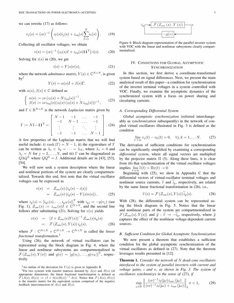
Using (26), the network of virtual oscillators can berepresented using the block diagram in Fig. 4, where thelinear and nonlinear subsystems are compartmentalized inF (Zosc(s), Y (s)) and g(v) = [g(v1), . . . , g(vN )]
T, respec-tively.
2An outline of the derivation for Y (s) is given in Appendix B.3For two systems with transfer matrices denoted by A(s) and B(s) (of
appropriate dimension), the linear fractional transformation is defined asF (A(s), B(s)) := (I +A(s)B(s))−1 A(s). Notice that F (A(s), B(s))is the transfer matrix for the equivalent system comprised of the negativefeedback interconnection of A(s) and B(s).
gi v
)v(g−
))s(, Y)s(oscZ(F
Figure 4: Block-diagram representation of the parallel inverter systemwith VOC with the linear and nonlinear subsystems clearly compart-mentalized.
IV. CONDITIONS FOR GLOBAL ASYMPTOTICSYNCHRONIZATION
In this section, we first derive a coordinate-transformedsystem based on signal differences. Next, we present the mainanalytical result of this paper—a condition for synchronizationof the inverter terminal voltages in a system controlled withVOC. Finally, we examine the asymptotic dynamics of thesynchronized system with a focus on power sharing andcirculating currents.
A. Corresponding Differential System
Global asymptotic synchronization (referred interchange-ably as synchronization subsequently) in the network of cou-pled virtual oscillators illustrated in Fig. 3 is defined as thecondition
limt→∞
vj(t)− vk(t) = 0, ∀j, k = 1, . . . N. (27)
The derivation of sufficient conditions for synchronizationcan be significantly simplified by examining a correspondingdifferential system, where all signal vectors are multipliedby the projector matrix Π (5). Along these lines, it is clearfrom (6) that synchronization of the virtual oscillator voltagesimplies lim
t→∞v(t) = Πv(t)→ 0.
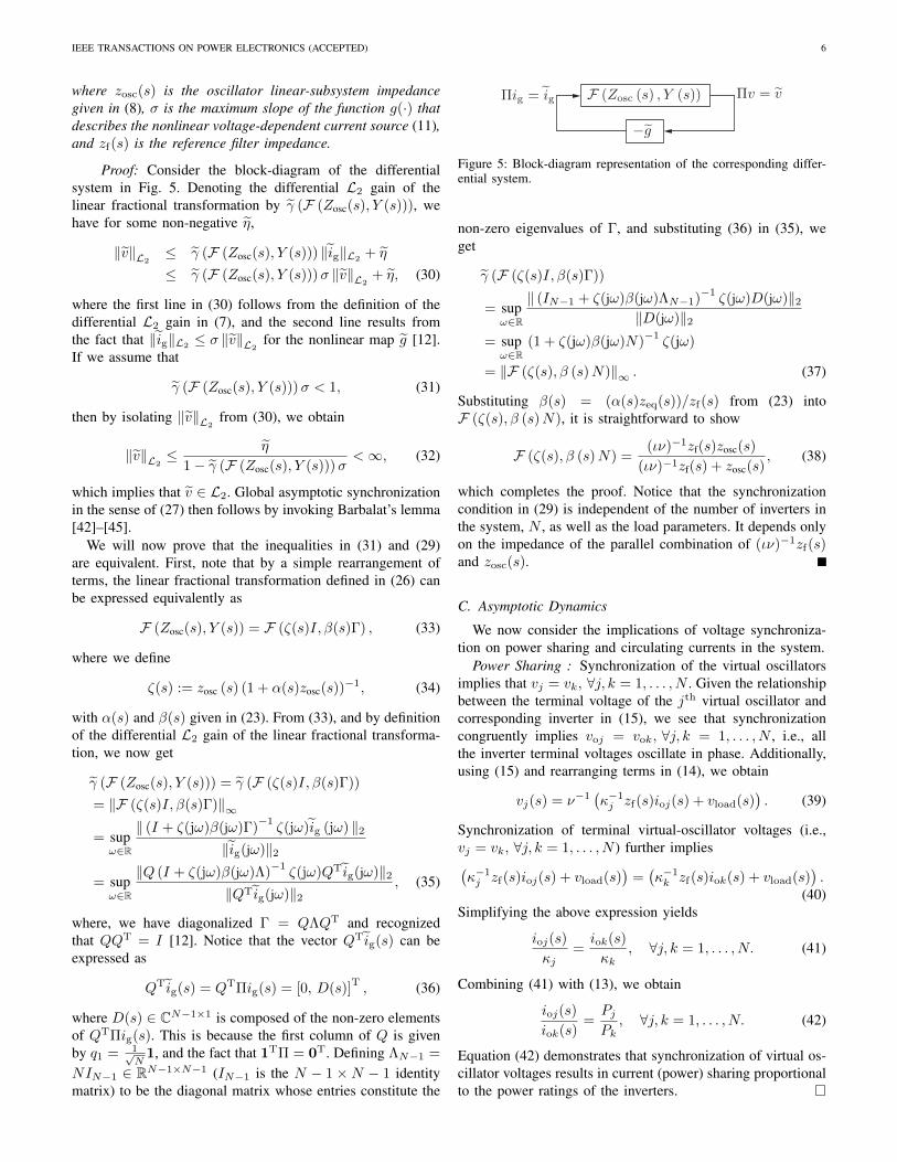
Beginning with (25), we show in Appendix C that thedifferential vectors of virtual-oscillator terminal voltages andnonlinear source currents, v and ig, respectively, are relatedby the same linear fractional transformation in (26), i.e.,
v (s) = F (Zosc(s), Y (s)) ig(s). (28)
With (28), the differential system can be represented us-ing the block diagram in Fig. 5. Notice that the linearand nonlinear parts of the system are compartmentalized inF (Zosc(s), Y (s)) and g : v → −ig, respectively, where gcaptures the effect of the nonlinear voltage-dependent currentsources.
B. Sufficient Condition for Global Asymptotic Synchronization
We now present a theorem that establishes a sufficientcondition for the global asymptotic synchronization of thevirtual oscillators as defined in (27). Note that the theoremleverages results presented in [12].
Theorem 1. Consider the network of N dead-zone oscillatorsinterfaced to the system of parallel inverters with current andvoltage gains, ι and ν, as shown in Fig. 3. The system ofoscillators synchronizes in the sense of (27), if
supω∈R
∥∥∥∥(ιν)−1zf(jω)zosc (jω)
(ιν)−1zf(jω) + zosc (jω)
∥∥∥∥2
σ < 1, (29)
IEEE TRANSACTIONS ON POWER ELECTRONICS (ACCEPTED) 6
where zosc(s) is the oscillator linear-subsystem impedancegiven in (8), σ is the maximum slope of the function g(·) thatdescribes the nonlinear voltage-dependent current source (11),and zf(s) is the reference filter impedance.
Proof: Consider the block-diagram of the differentialsystem in Fig. 5. Denoting the differential L2 gain of thelinear fractional transformation by γ (F (Zosc(s), Y (s))), wehave for some non-negative η,
‖v‖L2≤ γ (F (Zosc(s), Y (s))) ‖ig‖L2
+ η
≤ γ (F (Zosc(s), Y (s)))σ ‖v‖L2+ η, (30)
where the first line in (30) follows from the definition of thedifferential L2 gain in (7), and the second line results fromthe fact that ‖ig‖L2 ≤ σ ‖v‖L2
for the nonlinear map g [12].If we assume that
γ (F (Zosc(s), Y (s)))σ < 1, (31)
then by isolating ‖v‖L2from (30), we obtain
‖v‖L2≤ η
1− γ (F (Zosc(s), Y (s)))σ<∞, (32)
which implies that v ∈ L2. Global asymptotic synchronizationin the sense of (27) then follows by invoking Barbalat’s lemma[42]–[45].
We will now prove that the inequalities in (31) and (29)are equivalent. First, note that by a simple rearrangement ofterms, the linear fractional transformation defined in (26) canbe expressed equivalently as
F (Zosc(s), Y (s)) = F (ζ(s)I, β(s)Γ) , (33)
where we define
ζ(s) := zosc (s) (1 + α(s)zosc(s))−1, (34)
with α(s) and β(s) given in (23). From (33), and by definitionof the differential L2 gain of the linear fractional transforma-tion, we now get
γ (F (Zosc(s), Y (s))) = γ (F (ζ(s)I, β(s)Γ))
= ‖F (ζ(s)I, β(s)Γ)‖∞= sup
ω∈R
‖ (I + ζ(jω)β(jω)Γ)−1ζ(jω)ig (jω) ‖2
‖ig(jω)‖2
= supω∈R
‖Q (I + ζ(jω)β(jω)Λ)−1ζ(jω)QTig(jω)‖2
‖QTig(jω)‖2, (35)
where, we have diagonalized Γ = QΛQT and recognizedthat QQT = I [12]. Notice that the vector QTig(s) can beexpressed as
QTig(s) = QTΠig(s) = [0, D(s)]T, (36)
where D(s) ∈ CN−1×1 is composed of the non-zero elementsof QTΠig(s). This is because the first column of Q is givenby q1 = 1√
N1, and the fact that 1TΠ = 0T. Defining ΛN−1 =
NIN−1 ∈ RN−1×N−1 (IN−1 is the N − 1 ×N − 1 identitymatrix) to be the diagonal matrix whose entries constitute the
g−
gi=giΠ v=vΠ))s(, Y)s(oscZ(F
Figure 5: Block-diagram representation of the corresponding differ-ential system.
non-zero eigenvalues of Γ, and substituting (36) in (35), weget
γ (F (ζ(s)I, β(s)Γ))
= supω∈R
‖ (IN−1 + ζ(jω)β(jω)ΛN−1)−1ζ(jω)D(jω)‖2
‖D(jω)‖2= sup
ω∈R(1 + ζ(jω)β(jω)N)
−1ζ(jω)
= ‖F (ζ(s), β (s)N)‖∞ . (37)
Substituting β(s) = (α(s)zeq(s))/zf(s) from (23) intoF (ζ(s), β (s)N), it is straightforward to show
F (ζ(s), β (s)N) =(ιν)−1zf(s)zosc(s)
(ιν)−1zf(s) + zosc(s), (38)
which completes the proof. Notice that the synchronizationcondition in (29) is independent of the number of inverters inthe system, N , as well as the load parameters. It depends onlyon the impedance of the parallel combination of (ιν)−1zf(s)and zosc(s).
C. Asymptotic Dynamics
We now consider the implications of voltage synchroniza-tion on power sharing and circulating currents in the system.
Power Sharing : Synchronization of the virtual oscillatorsimplies that vj = vk, ∀j, k = 1, . . . , N . Given the relationshipbetween the terminal voltage of the jth virtual oscillator andcorresponding inverter in (15), we see that synchronizationcongruently implies voj = vok, ∀j, k = 1, . . . , N , i.e., allthe inverter terminal voltages oscillate in phase. Additionally,using (15) and rearranging terms in (14), we obtain
vj(s) = ν−1(κ−1j zf(s)ioj(s) + vload(s)
). (39)
Synchronization of terminal virtual-oscillator voltages (i.e.,vj = vk, ∀j, k = 1, . . . , N ) further implies(κ−1j zf(s)ioj(s) + vload(s)
)=(κ−1k zf(s)iok(s) + vload(s)
).
(40)Simplifying the above expression yields
ioj(s)
κj=iok(s)
κk, ∀j, k = 1, . . . , N. (41)
Combining (41) with (13), we obtain
ioj(s)
iok(s)=Pj
Pk, ∀j, k = 1, . . . , N. (42)
Equation (42) demonstrates that synchronization of virtual os-cillator voltages results in current (power) sharing proportionalto the power ratings of the inverters.
IEEE TRANSACTIONS ON POWER ELECTRONICS (ACCEPTED) 7
Elimination of Circulating Currents : We now establish thatcirculating currents decay to zero as the terminal voltagesin the system of parallel inverters synchronize. Adoptingthe definition of circulating currents proposed in [55], thecirculating component of the jth inverter output current isdenoted by icj(s), and defined as
and the vector of all circulating currents, ic(s) =[ic1(s), . . . , icN (s)]T, is given by
ic(s) = io(s)− io(s)T1
κT1κ. (45)
Since the terminal voltages of the inverters synchronizeasymptotically, in periodic steady state we can write the vectorof terminal inverter voltages as vo(s) = vo(s)1, where vo(s)denotes the synchronized terminal voltage of the inverters.With this notation in place and assuming synchronized op-eration, we can express the vector of output currents in (14)as
io(s) =vo(s)− vload(s)
zf(s)diag κ1, . . . , κN1
=vo(s)− vload(s)
zf(s)κ. (46)
Substituting (46) in (45), we obtain
ic(s) =vo(s)− vload(s)
zf(s)κ− (vo(s)− vload(s))κT1
zf(s)κT1κ = 0,
(47)which demonstrates that synchronization of the inverter ter-minal voltages results in the circulating currents decaying tozero in periodic steady state.
o1ιi
1v)1v(g
g1i
o1v
fz
ι
outv
open-circuittest
rated-loadtest
ϕσ
−
+
R L C
ν1P
min2V
o1i
1v
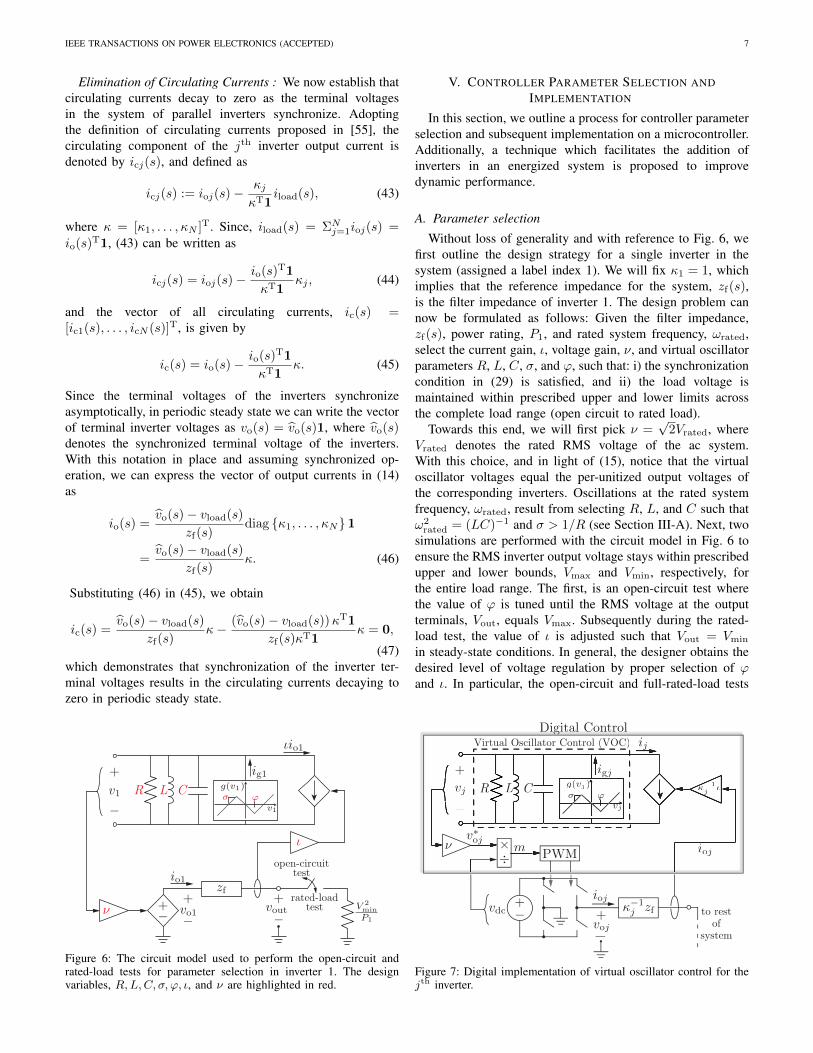
Figure 6: The circuit model used to perform the open-circuit andrated-load tests for parameter selection in inverter 1. The designvariables, R,L,C, σ, ϕ, ι, and ν are highlighted in red.
V. CONTROLLER PARAMETER SELECTION ANDIMPLEMENTATION
In this section, we outline a process for controller parameterselection and subsequent implementation on a microcontroller.Additionally, a technique which facilitates the addition ofinverters in an energized system is proposed to improvedynamic performance.
A. Parameter selection
Without loss of generality and with reference to Fig. 6, wefirst outline the design strategy for a single inverter in thesystem (assigned a label index 1). We will fix κ1 = 1, whichimplies that the reference impedance for the system, zf(s),is the filter impedance of inverter 1. The design problem cannow be formulated as follows: Given the filter impedance,zf(s), power rating, P1, and rated system frequency, ωrated,select the current gain, ι, voltage gain, ν, and virtual oscillatorparameters R, L, C, σ, and ϕ, such that: i) the synchronizationcondition in (29) is satisfied, and ii) the load voltage ismaintained within prescribed upper and lower limits acrossthe complete load range (open circuit to rated load).
Towards this end, we will first pick ν =√
2Vrated, whereVrated denotes the rated RMS voltage of the ac system.With this choice, and in light of (15), notice that the virtualoscillator voltages equal the per-unitized output voltages ofthe corresponding inverters. Oscillations at the rated systemfrequency, ωrated, result from selecting R, L, and C such thatω2rated = (LC)−1 and σ > 1/R (see Section III-A). Next, two
simulations are performed with the circuit model in Fig. 6 toensure the RMS inverter output voltage stays within prescribedupper and lower bounds, Vmax and Vmin, respectively, forthe entire load range. The first, is an open-circuit test wherethe value of ϕ is tuned until the RMS voltage at the outputterminals, Vout, equals Vmax. Subsequently during the rated-load test, the value of ι is adjusted such that Vout = Vmin
in steady-state conditions. In general, the designer obtains thedesired level of voltage regulation by proper selection of ϕand ι. In particular, the open-circuit and full-rated-load tests
jgi
ji
)jv(g
fzj1−κ
jov
ϕσ
−+
−
+
Virtual Oscillator Control (VOC)
to rest of
system
Digital Control
R L C
PWM
−+ joi
joi
dcv
jv
m
ιj1−κ
jgi
ji
−
+
Virtual Oscillator Control (VOC)
Digital Control
R L C
PWM
)jv(gϕσ
joi
jv
m
ιj1−κ
ν jo∗v
jv
×÷
Figure 7: Digital implementation of virtual oscillator control for thejth inverter.
IEEE TRANSACTIONS ON POWER ELECTRONICS (ACCEPTED) 8
ensure that the values of ϕ and ι are chosen in proportion toVmax and (Vmax − Vmin), respectively. Finally, the parametersare tuned to reduce the value of ε =
√L/C (σ − 1/R) such
that the synchronization condition in (29) is satisfied.Inverters with differing power ratings are easily accom-
modated by appropriately selecting the value of κj for j =2, . . . , N as dictated by (13). Since κ1 = 1, it follows thatκj = Pj/P1. The remaining parameters are identical to thoseused in inverter 1.
B. Controller Implementation
After completing the parameter-selection process outlinedabove, the resulting controller can be implemented straightfor-wardly on a standard microcontroller, as shown in Fig. 7, bydiscretizing the second-order system in (12) which describesthe dead-zone oscillator dynamics. With reference to thecontroller depicted in Fig. 7, the measured output currentof the jth inverter is scaled by κ−1j ι and extracted fromthe virtual oscillator. The resulting oscillator voltage, vj , ismultiplied by ν to generate an ac voltage command, denotedv∗oj . After normalizing the voltage command with respect tothe dc-link voltage, sine-triangle PWM can be applied to themodulation signal, m, to generate the switching signals. As aresult of this strategy, the average inverter ac voltage followsthe commanded voltage, i.e., voj → v∗oj = νvj . Furthermore,notice from Fig. 7 that the voltage command, v∗oj , is scaledby the instantaneously measured dc bus voltage, vdc, therebyensuring that the dc link dynamics are decoupled from theoscillator-based controller. This strategy follows from well-established methods for decoupling dc-link dynamics fromoutput ac-control dynamics [56]. Notice that the controlleronly requires the output current and dc-link voltage measure-ments. Furthermore, the proposed control does not require realand reactive power computations, a phase-locked loop, or anytrigonometric functions.
addt
addt
loadv
loadv
−+
−+
Digital Controlpre-synchronization circuit
fzj1−κ
−
+ VOC
PWM
−+ joi
joi
dcv
jv
m ιj1−κ
fz1−)νι(
to rest of
system
addt
loadv
−+
Digital Controlpre-synchronization circuit
−
+ VOC
PWM joi
jv
m ιj1−κ
fz1−)νι(
ν jo∗v
shuntr
1−ν
seriesrji
×÷
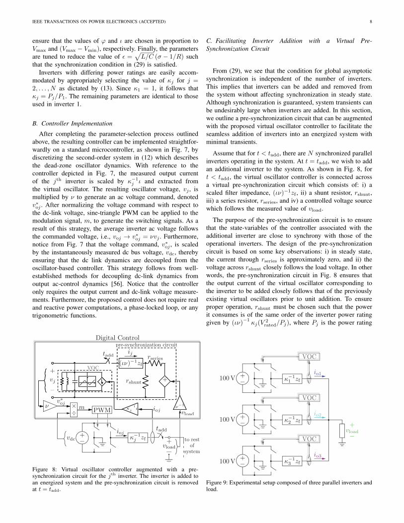
Figure 8: Virtual oscillator controller augmented with a pre-synchronization circuit for the jth inverter. The inverter is added toan energized system and the pre-synchronization circuit is removedat t = tadd.
C. Facilitating Inverter Addition with a Virtual Pre-Synchronization Circuit
From (29), we see that the condition for global asymptoticsynchronization is independent of the number of inverters.This implies that inverters can be added and removed fromthe system without affecting synchronization in steady state.Although synchronization is guaranteed, system transients canbe undesirably large when inverters are added. In this section,we outline a pre-synchronization circuit that can be augmentedwith the proposed virtual oscillator controller to facilitate theseamless addition of inverters into an energized system withminimal transients.
Assume that for t < tadd, there are N synchronized parallelinverters operating in the system. At t = tadd, we wish to addan additional inverter to the system. As shown in Fig. 8, fort < tadd, the virtual oscillator controller is connected acrossa virtual pre-synchronization circuit which consists of: i) ascaled filter impedance, (ιν)−1zf , ii) a shunt resistor, rshunt,iii) a series resistor, rseries, and iv) a controlled voltage sourcewhich follows the measured value of vload.
The purpose of the pre-synchronization circuit is to ensurethat the state-variables of the controller associated with theadditional inverter are close to synchrony with those of theoperational inverters. The design of the pre-synchronizationcircuit is based on some key observations: i) in steady state,the current through rseries is approximately zero, and ii) thevoltage across rshunt closely follows the load voltage. In otherwords, the pre-synchronization circuit in Fig. 8 ensures thatthe output current of the virtual oscillator corresponding tothe inverter to be added closely follows that of the previouslyexisting virtual oscillators prior to unit addition. To ensureproper operation, rshunt must be chosen such that the powerit consumes is of the same order of the inverter power ratinggiven by (ιν)
−1κj(V
2rated/Pj), where Pj is the power rating
100V
100V
100V
loadv
fz21−κ
−+
−+
−+
−+ o1i
o2i
o3i
fz11−κ
fz31−κ
VOC
VOC
VOC
Figure 9: Experimental setup composed of three parallel inverters andload.
IEEE TRANSACTIONS ON POWER ELECTRONICS (ACCEPTED) 9
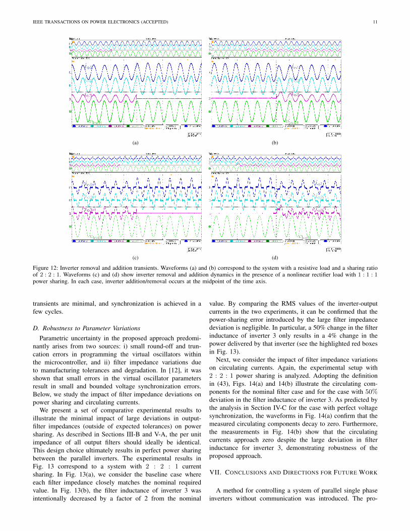
(a) (b)
(c) (d)
Figure 10: Load voltage and inverter currents during startup with non-identical initial conditions. Waveforms in (a) and (b) demonstratesystem behavior when connected to a resistive load under 1 : 1 : 1 and 2 : 2 : 1 ratios of power sharing, respectively. Waveforms in (c) and(d) correspond to the case of equal power sharing with RLC and nonlinear diode-bridge rectifier loads, respectively.
of the jth inverter.4 Finally, rseries should be picked sufficientlysmall such that a low impedance path exists between theload following voltage source and rshunt. When the inverteris added at t = tadd, the pre-synchronization circuit isdisconnected, such that the original VOC controller in Fig. 7is recovered.
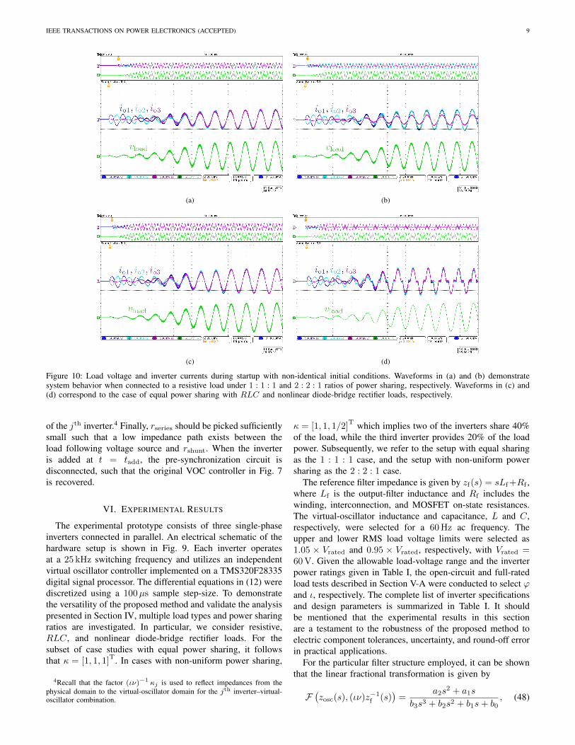
VI. EXPERIMENTAL RESULTS
The experimental prototype consists of three single-phaseinverters connected in parallel. An electrical schematic of thehardware setup is shown in Fig. 9. Each inverter operatesat a 25 kHz switching frequency and utilizes an independentvirtual oscillator controller implemented on a TMS320F28335digital signal processor. The differential equations in (12) werediscretized using a 100µs sample step-size. To demonstratethe versatility of the proposed method and validate the analysispresented in Section IV, multiple load types and power sharingratios are investigated. In particular, we consider resistive,RLC, and nonlinear diode-bridge rectifier loads. For thesubset of case studies with equal power sharing, it followsthat κ = [1, 1, 1]
T. In cases with non-uniform power sharing,
4Recall that the factor (ιν)−1 κj is used to reflect impedances from thephysical domain to the virtual-oscillator domain for the jth inverter–virtual-oscillator combination.
κ = [1, 1, 1/2]T which implies two of the inverters share 40%
of the load, while the third inverter provides 20% of the loadpower. Subsequently, we refer to the setup with equal sharingas the 1 : 1 : 1 case, and the setup with non-uniform powersharing as the 2 : 2 : 1 case.
The reference filter impedance is given by zf(s) = sLf+Rf ,where Lf is the output-filter inductance and Rf includes thewinding, interconnection, and MOSFET on-state resistances.The virtual-oscillator inductance and capacitance, L and C,respectively, were selected for a 60 Hz ac frequency. Theupper and lower RMS load voltage limits were selected as1.05 × Vrated and 0.95 × Vrated, respectively, with Vrated =60 V. Given the allowable load-voltage range and the inverterpower ratings given in Table I, the open-circuit and full-ratedload tests described in Section V-A were conducted to select ϕand ι, respectively. The complete list of inverter specificationsand design parameters is summarized in Table I. It shouldbe mentioned that the experimental results in this sectionare a testament to the robustness of the proposed method toelectric component tolerances, uncertainty, and round-off errorin practical applications.
For the particular filter structure employed, it can be shownthat the linear fractional transformation is given by
F(zosc(s), (ιν)z−1f (s)
)=
a2s2 + a1s
b3s3 + b2s2 + b1s+ b0, (48)
IEEE TRANSACTIONS ON POWER ELECTRONICS (ACCEPTED) 10
(a) (b)
(c) (d)
Figure 11: Waveforms in (a) and (b) demonstrate the system transient response with 2 : 2 : 1 power sharing during a step up and step downin resistive load. Waveforms in (c) and (d) correspond to load steps with an RLC load. The dashed lines illustrate the change in powerfactor after each load transient. In each case, the load transient occurs at the midpoint of the time axis.
where a2 = Lf , a1 = Rf , b3 = LfC, b2 = (Lf/R) + RfC,b1 = (Lf/L) + (Rf/R) + ιν, and b0 = Rf/L. Evaluating(29) with the values given in Table I, it can be shown that∥∥F(zosc(jω), (ιν)z−1f (jω
)∥∥∞ σ = 0.77 < 1, which guaran-
tees synchronization.
A. Start up
First, we consider the case when all three inverters aresimultaneously energized from a cold-start. To emulate er-rors which may exist in a practical system, each inverter isprogrammed with non identical initial conditions, i.e., initialconditions for the three virtual oscillator voltages were se-lected to be (1/ν) [5 V, 4 V, 3 V]
T. Figs. 10(a)–10(b) show theinverter currents and load voltage from startup in the presenceof a resistive load under uniform and nonuniform sharing,respectively. The waveforms in Figs. 10(c)–10(d) illustratestartup system dynamics with an RLC load and nonlinearrectifier load, respectively. The RLC load impedance is givenby (Rrlc + sLrlc)||(Rrlc + (sCrlc)
−1); the values of Rrlc, Lrlc,and Crlc are listed in Table I.
B. Load transients
System responses to load transients are illustrated in Fig. 11.In particular, Figs. 11(a)–11(b) depict the transient response
to step changes in a resistive load with 2 : 2 : 1 powersharing. It can be observed that the increase in output currentis nearly instantaneous with changes in the load and that theload voltage is unperturbed. The waveforms in Figs. 11(c)–11(d) correspond to an RLC load where the load is changedfrom (Rrlc + sLrlc) ‖
(Rrlc + (sCrlc)
−1) ↔ (Rrlc + sLrlc).Note that the change in power factor (denoted by dashed lines)coincides with the instant at which the series RC componentof the RLC load is switched in and out. There are no dccomponents in the periodic steady-state waveforms.
C. Inverter addition and removal
Here we investigate the system dynamics as inverters areremoved from and added into an energized system. Thevirtual pre-synchronization circuit described in Section V-C,and illustrated in Fig. 8 was utilized to facilitate inverteraddition. Figs. 12(a) and 12(c) show the transient response asthe third inverter is removed from the system with resistive andrectifier loads, respectively. Notice that the remaining invertersabruptly increase their current output when the third inverteris removed, which ensures that the load voltage continues tomeet specifications. The waveforms in Figs. 12(b) and 12(d)illustrate system behavior when the third inverter is added intothe system. Despite the sudden inclusion of the third inverter,
IEEE TRANSACTIONS ON POWER ELECTRONICS (ACCEPTED) 11
(a) (b)
(c) (d)
Figure 12: Inverter removal and addition transients. Waveforms (a) and (b) correspond to the system with a resistive load and a sharing ratioof 2 : 2 : 1. Waveforms (c) and (d) show inverter removal and addition dynamics in the presence of a nonlinear rectifier load with 1 : 1 : 1power sharing. In each case, inverter addition/removal occurs at the midpoint of the time axis.
transients are minimal, and synchronization is achieved in afew cycles.
D. Robustness to Parameter Variations
Parametric uncertainty in the proposed approach predomi-nantly arises from two sources: i) small round-off and trun-cation errors in programming the virtual oscillators withinthe microcontroller, and ii) filter impedance variations dueto manufacturing tolerances and degradation. In [12], it wasshown that small errors in the virtual oscillator parametersresult in small and bounded voltage synchronization errors.Below, we study the impact of filter impedance deviations onpower sharing and circulating currents.
We present a set of comparative experimental results toillustrate the minimal impact of large deviations in output-filter impedances (outside of expected tolerances) on powersharing. As described in Sections III-B and V-A, the per unitimpedance of all output filters should ideally be identical.This design choice ultimately results in perfect power sharingbetween the parallel inverters. The experimental results inFig. 13 correspond to a system with 2 : 2 : 1 currentsharing. In Fig. 13(a), we consider the baseline case whereeach filter impedance closely matches the nominal requiredvalue. In Fig. 13(b), the filter inductance of inverter 3 wasintentionally decreased by a factor of 2 from the nominal
value. By comparing the RMS values of the inverter-outputcurrents in the two experiments, it can be confirmed that thepower-sharing error introduced by the large filter impedancedeviation is negligible. In particular, a 50% change in the filterinductance of inverter 3 only results in a 4% change in thepower delivered by that inverter (see the highlighted red boxesin Fig. 13).
Next, we consider the impact of filter impedance variationson circulating currents. Again, the experimental setup with2 : 2 : 1 power sharing is analyzed. Adopting the definitionin (43), Figs. 14(a) and 14(b) illustrate the circulating com-ponents for the nominal filter case and for the case with 50%deviation in the filter inductance of inverter 3. As predicted bythe analysis in Section IV-C for the case with perfect voltagesynchronization, the waveforms in Fig. 14(a) confirm that themeasured circulating components decay to zero. Furthermore,the measurements in Fig. 14(b) show that the circulatingcurrents approach zero despite the large deviation in filterinductance for inverter 3, demonstrating robustness of theproposed approach.
VII. CONCLUSIONS AND DIRECTIONS FOR FUTURE WORK
A method for controlling a system of parallel single phaseinverters without communication was introduced. The pro-
IEEE TRANSACTIONS ON POWER ELECTRONICS (ACCEPTED) 12
(a)
(b)
Figure 13: Measurements corresponding to three parallel invertersserving a resistive load with a 2 : 2 : 1 current sharing ratio. Thewaveforms in (a) correspond to the ideal case where the filter valuesclosely match the nominal values and the results in (b) correspondto the case where the filter inductance of inverter 3 is intentionallyreduced by 50% from the nominal value. Despite the large deviationof filter impedance in (b), the impact on current sharing accuracy isnegligible. Comparing the two experiments, a modest 4% change inthe power delivered by inverter 3 is observed.
posed technique, referred to as virtual oscillator control, relieson programming the controller of each inverter such that theinverter emulates the dynamics of a dead-zone oscillator cir-cuit. It was shown that the system of N inverters synchronizetheir ac outputs and share the load in proportion to their powerrating without communication. In addition, a method whichfacilitates the addition of inverters into an energized systemwas developed. A sufficient condition for virtual oscillatorsynchronization was derived and the result was shown to beindependent of the load and the number of inverters. Experi-mental results validated the proposed control approach withuniform and non-uniform power sharing between inverterswhile connected to both linear and nonlinear loads.
Compelling avenues for future work include developingsimilar virtual-oscillator based controllers for grid connectedapplications. Furthermore, although there are no practicalbarriers to the use of LC and LCL filters, the analyticalframework should be extended to accommodate these addi-tional filter structures. Furthermore, although it was experi-mentally shown that the proposed method exhibits robustness
t [s]
i c1,i
c2,i
c3[A
]i o
1,i
o2,i
o3[A
]
0 0.05 0.1 0.15 0.2 0.25 0.3
−0.5
0
0.5
−0.5
0
0.5
0.35
(a)
i c1,i
c2,i
c3[A
]i o
1,i
o2,i
o3[A
]t [s]
0 0.05 0.1 0.15 0.2 0.25 0.3
−0.5
0
0.5
−0.5
0
0.5
0.35
(b)
Figure 14: Measured circulating currents during startup under 2 : 2 :1 sharing with a resistive load. Nominal filter values were used in (a).In (b), filter inductance 3 was deliberately halved from the nominaldesign value. In both cases, the circulating currents, ic1, ic2, and ic3,approach zero with asymptotic voltage synchronization.
to filter parameter deviations, future efforts could be focusedon analytically quantifying robustness margins. Finally, whilethe analysis and experiments in this paper are focused oncontroller-time-scale synchronization phenomena, it is impor-tant to analyze switch-level dynamic phenomena of interestwith VOC. It would be of interest to determine whether thereare benefits associated with PWM carrier synchronization ordc bus coordination, even though experimental results haveshown that these are not required.
APPENDIX
A. Experimental parameters
The inverter hardware specifications and control parametersare listed below in Table I. The virtual oscillator parameters areR, L, C, σ, and ϕ. The voltage and current scaling gains aredenoted as ν and ι, respectively. System voltage and frequencyratings are ωrated and Vrated, respectively. Using the designprocedure in Section V-A, the upper and lower voltage limitsare Vmax and Vmin, respectively. The nominal inverter filterimpedance is zf(s) = Rf + sLf . The jth inverter powerrating is denoted as Pj and the accompanying power ratingscaling factors are denoted as κ1, κ2, and κ3. The maximumrated RMS output current of the nominal inverter design isdenoted as Imax. The pre-synchronization circuit parameters,as described in Section V-C, are denoted as rseriesj and rshuntj .
IEEE TRANSACTIONS ON POWER ELECTRONICS (ACCEPTED) 13
The RLC load parameters are denoted by Rrlc, Lrlc, andCrlc. The resulting voltage regulation curve for the selectedparamaters is given in Fig. 15.
Table I: Experimental hardware and controller parameters.
ωrated = 2π60 rad s−1 Rf = 1 ΩVrated = 60 V Lf = 6 mH
Vmax = 1.05× Vrated κ1, κ2 = 1
Vmin = 0.95× Vrated κ3 = 1, 12
R = 10 Ω Imax = 2−12 0.8 A
L = 500µH Pj = κjImaxVmin
C = 1/(Lω2
rated
)rseriesj = 100
κj
ινΩ
σ = 1 S rshuntj = 2Pj
I2max
κj
ιν
ϕ = 0.4695 V Rrlc = 50 Ωι = 0.1125 Lrlc = 37 mH
ν =√
2Vrated Crlc = 48µF
B. Derivation of Y (s)
From (20), we see that the inverse of the admittance matrixis given by
Y −1(s) =zf(s)
ιν
(I +
zeq(s)
zf(s)11T
). (49)
For an invertible square matrix A, and vectors x, y, theSherman-Morrison-Woodbury formula [57] states
(A+ xyT)−1 = A−1 − A−1xyTA−1
1 + yTA−1x. (50)
Applying this to invert (49), we get
Y (s) =ιν
zf(s)
(I − (zeq(s)/zf(s))11
T
1 + (zeq(s)/zf(s))1T1
). (51)
Recognizing that 1T1 = N , and the fact that 11T = NI −Γ,we can simplify (51) to obtain
Y (s) =ιν
zf(s)(zf(s) +Nzeq(s))(zf(s)I + zeq(s)Γ) , (52)
which is of the form Y (s) = α(s)I + β(s)Γ, with α(s) andβ(s) given in (23).
ratedPoutP
0 0.2 0.4 0.6 0.8 10.9
0.95
1
1.05
1.1
outV
[pu]
maxV
minV
Figure 15: The voltage regulation curve corresponding to the ex-perimental setup. Using the open-circuit and full-rated-load tests, thevalues of ϕ and ι were tuned such that the load voltage is maintainedbetween ±5% of the rated value of the entire load range.
C. Derivation of (28)Begin by pre-multiplying both sides of (25) by the projector
matrix, Π, to obtain
Πv(s) = ΠZosc(s) (ig(s)− i(s))= Zosc(s)
(ig(s)−ΠY (s)v(s)
). (53)
The second line in (53) follows from recognizing thatΠZosc(s) = Πzosc(s)I = zosc(s)IΠ = Zosc(s)Π, andsubstituting for i(s) from (21). Next, it is straightforward toshow that the projector and admittance matrices commute:
ΠY (s) = Π (α(s)I + β(s)Γ)
= α(s)Π + β(s)ΠΓ
= α(s)Π + β(s)
(I − 1
N11T
)Γ
= α(s)Π + β(s)
(ΓI − 1
NΓ11T
)
= (α(s)I + β(s)Γ) Π = Y (s)Π, (54)
where we have used 11TΓ = 00T = Γ11T (which followsfrom the fact that the row and column sums of Γ are zero).Using ΠY (s) = Y (s)Π in (53), we get
v(s) = Zosc(s)(ig(s)− Y (s)v(s)
). (55)
Isolating v(s), we can then write
v(s) = (I + Zosc(s)Y (s))−1Zosc(s)ig
= F (Zosc(s), Y (s)) ig(s). (56)
REFERENCES
[1] J.-F. Chen and C.-L. Chu, “Combination voltage-controlled and current-controlled PWM inverters for UPS parallel operation,” IEEE Trans.Power Electron., vol. 10, pp. 547–558, Sept. 1995.
[2] Y. Xue, L. Chang, S. B. Kjaer, J. Bordonau, and T. Shimizu, “Topologiesof single-phase inverters for small distributed power generators: Anoverview,” IEEE Trans. Power Electron., vol. 19, pp. 1305–1314, Sept.2004.
[3] Y. A. R. I. Mohamed and E. El-Saadany, “Adaptive decentralized droopcontroller to preserve power sharing stability of paralleled inverters indistributed generation microgrids,” IEEE Trans. Power Electron., vol. 23,pp. 2806–2816, Nov. 2008.
[4] D. De and V. Ramanarayanan, “Decentralized parallel operation ofinverters sharing unbalanced and nonlinear loads,” IEEE Trans. PowerElectron., vol. 25, pp. 3015–3025, Dec. 2010.
[5] B. Johnson, A. Davoudi, P. Chapman, and P. Sauer, “Microgrid dynamicscharacterization using the automated state model generation algorithm,”in IEEE Proc. Int. Symp. on Circuits and Syst., pp. 2758–2761, June2010.
[6] B. Johnson, A. Davoudi, P. Chapman, and P. Sauer, “A unified dynamiccharacterization framework for microgrid systems,” Electric Power Com-ponents and Systems, vol. 40, pp. 93–111, Nov. 2011.
[7] R. Bojoi, L. Limongi, D. Roiu, and A. Tenconi, “Enhanced power qualitycontrol strategy for single-phase inverters in distributed generationsystems,” IEEE Trans. Power Electron., vol. 26, pp. 798–806, Mar. 2011.
[8] M. Borrega, L. Marroyo, R. Gonzalez, J. Balda, and J. Agorreta,“Modeling and control of a master-slave PV inverter with N-paralleledinverters and three-phase three-limb inductors,” IEEE Trans. PowerElectron., vol. 28, pp. 2842–2855, June 2013.
[9] WeiYu, D. Xu, and C. Zhou, “Parallel control of the UPS inverters,” inApplied Power Electron. Conf. and Expo., pp. 939–944, 2008.
[10] A. Bezzolato, M. Carmeli, L. Frosio, G. Marchegiani, and M. Mauri,“Reduction of high frequency zero sequence harmonics in parallelconnected PV-inverters,” in European Conf. Power Electron. and Appl.,pp. 1–10, 2011.
IEEE TRANSACTIONS ON POWER ELECTRONICS (ACCEPTED) 14
[11] K.-H. Kim and D.-S. Hyun, “A high performance DSP voltage controllerwith PWM synchronization for parallel operation of UPS systems,” inPower Electron. Spec. Conf., pp. 1–7, 2006.
[12] B. B. Johnson, S. V. Dhople, A. O. Hamadeh, and P. T. Krein,“Synchronization of nonlinear oscillators in an LTI electrical network,”IEEE Trans. Circuits Syst. I: Fundam. Theory Appl., 2013. To Appear.
[13] B. Johnson, Control, analysis, and design of distributed inverter systems.PhD thesis, Univ. of Illinois at Urbana-Champaign, Urbana, IL, May2013.
[14] B. B. Johnson, S. V. Dhople, J. L. Cale, A. O. Hamadeh, and P. T. Krein,“Oscillator-based inverter control for islanded three-phase microgrids,”IEEE Journ. Photovoltaics, 2013. To appear.
[15] M. Chandorkar, D. Divan, and R. Adapa, “Control of parallel connectedinverters in standalone ac supply systems,” IEEE Trans. Ind. Appl.,vol. 29, pp. 136–143, Jan. 1993.
[16] R. Lasseter, “Microgrids,” in IEEE Power Eng. Society Winter Meeting,vol. 1, pp. 305–308, 2002.
[17] M. Marwali, J.-W. Jung, and A. Keyhani, “Control of distributedgeneration systems - Part II: Load sharing control,” IEEE Trans. PowerElectron., vol. 19, pp. 1551–1561, Nov. 2004.
[18] P. Piagi and R. Lasseter, “Autonomous control of microgrids,” in IEEEPower Eng. Society General Meeting, vol. 1, pp. 1–8, June 2006.
[19] K. De Brabandere, B. Bolsens, J. Van den Keybus, A. Woyte, J. Driesen,and R. Belmans, “A voltage and frequency droop control method forparallel inverters,” IEEE Trans. Power Electron., vol. 22, pp. 1107–1115,July 2007.
[20] J. Kim, J. Guerrero, P. Rodriguez, R. Teodorescu, and K. Nam, “Modeadaptive droop control with virtual output impedances for an inverter-based flexible ac microgrid,” IEEE Trans. Power Electron., vol. 26,pp. 689–701, Mar. 2011.
[21] J. Rocabert, A. Luna, F. Blaabjerg, and P. Rodriguez, “Control of powerconverters in ac microgrids,” IEEE Trans. Power Electron., vol. 27,pp. 4734–4749, Nov. 2012.
[22] C.-T. Lee, C.-C. Chu, and P.-T. Cheng, “A new droop control methodfor the autonomous operation of distributed energy resource interfaceconverters,” IEEE Trans. Power Electron., vol. 28, pp. 1980–1993, Apr.2013.
[23] J. Guerrero, L. de Vicuna, J. Matas, M. Castilla, and J. Miret, “Awireless controller to enhance dynamic performance of parallel invertersin distributed generation systems,” IEEE Trans. Power Electron., vol. 19,pp. 1205–1213, Sept. 2004.
[24] J. Lopes, C. Moreira, and A. Madureira, “Defining control strategiesfor microgrids islanded operation,” IEEE Trans. Power Syst., vol. 21,pp. 916–924, May 2006.
[25] N. Pogaku, M. Prodanovic, and T. C. Green, “Modeling, analysis andtesting of autonomous operation of an inverter-based microgrid,” IEEETrans. Power Electron., vol. 22, pp. 613–625, Mar. 2007.
[26] J. M. Guerrero, J. C. Vasquez, J. Matas, L. G. de Vicuña, and M. Castilla,“Hierarchical control of droop-controlled ac and dc microgrids–Ageneral approach toward standardization,” IEEE Trans. Ind. Electron.,vol. 58, no. 1, pp. 158–172, 2011.
[27] J. He and Y. W. Li, “An enhanced microgrid load demand sharingstrategy,” IEEE Trans. Power Electron., vol. 27, pp. 3984–3995, Sept.2012.
[28] Q.-C. Zhong, “Robust droop controller for accurate proportional loadsharing among inverters operated in parallel,” IEEE Trans. Ind. Electron.,vol. 60, pp. 1281–1290, April 2013.
[29] Y. Kuramoto, Chemical Oscillations, Waves, and Turbulence. New York:Springer–Verlag, 1984.
[30] D. C. Michaels, E. P. Matyas, and J. Jalife, “Mechanisms of sinoatrialpacemaker synchronization-a new hypothesis,” Circulation Res., vol. 61,pp. 704–714, Nov. 1987.
[31] K. Wiesenfeld, P. Colet, and S. H. Strogatz, “Frequency locking inJosephson arrays: Connection with the Kuramoto model,” Phys. Rev.E, vol. 57, pp. 1563–1569, Feb. 1998.
[32] S. H. Strogatz, Nonlinear Dynamics And Chaos: With Applications ToPhysics, Biology, Chemistry, And Engineering. Studies in nonlinearity,Westview Press, First ed., Jan. 2001.
[33] F. Dörfler and F. Bullo, “Exploring synchronization in complex oscillatornetworks,” in IEEE Conf. on Decision and Control, (Maui, HI, USA),pp. 7157–7170, Dec. 2012.
[34] F. Dörfler and F. Bullo, “Synchronization and transient stability inpower networks and non-uniform Kuramoto oscillators,” SIAM Journ.on Control and Optimization, vol. 50, pp. 1616–1642, June 2012.
[35] J. W. Simpson-Porco, F. Dörfler, and F. Bullo, “Synchronization andpower sharing for droop-controlled inverters in islanded microgrids,”Automatica, 2013. In Press.
[36] N. Ainsworth and S. Grijalva, “A structure-preserving model and suffi-cient condition for frequency synchronization of lossless droop inverter-based AC networks,” IEEE Trans. Power Syst., 2013. in press.
[37] L. A. B. Tôrres, J. P. Hespanha, and J. Moehlis, “Power suppliessynchronization without communication,” in Proc. of the Power andEnergy Society General Meeting, July 2012.
[38] A. Pogromsky and H. Nijmeijer, “Cooperative oscillatory behavior ofmutually coupled dynamical systems,” IEEE Trans. Circuits Syst. I:Fundam. Theory Appl., vol. 48, pp. 152–162, Feb. 2001.
[39] G.-B. Stan, Global analysis and synthesis of oscillations: A dissipativityapproach. PhD thesis, Univ. of Liege, Belgium, May 2005.
[40] G.-B. Stan and R. Sepulchre, “Analysis of interconnected oscillators bydissipativity theory,” IEEE Trans. Autom. Control, vol. 52, pp. 256–270,Feb. 2007.
[41] M. Arcak, “Passivity as a design tool for group coordination,” IEEETrans. Autom. Control, vol. 52, pp. 1380–1390, Aug. 2007.
[42] A. Dhawan, A. Hamadeh, and B. Ingalls, “Designing synchronizationprotocols in networks of coupled nodes under uncertainty,” in AmericanControl Conf., pp. 4945–4950, June 2012.
[43] A. Hamadeh, Constructive Robust Synchronization of Networked ControlSystems. PhD thesis, Cambridge University, UK, June 2010.
[44] A. Hamadeh, G.-B. Stan, and J. Gonçalves, “Constructive Synchroniza-tion of Networked Feedback Systems,” in IEEE Conf. on Decision andControl, pp. 6710–6715, Dec. 2010.
[45] H. Khalil, Nonlinear Systems. Upper Saddle River, NJ: Prentice Hall,Third ed., 2002.
[46] A. Van der Schaft, L2-Gain and Passivity Techniques in NonlinearControl. Lecture Notes in Control and Information Sciences, London,UK: Springer, 1996.
[47] M. Liserre, F. Blaabjerg, and A. Dell’Aquila, “Step-by-step design pro-cedure for a grid-connected three-phase PWM voltage source converter,”International Journ. of Electron., vol. 91, no. 8, pp. 445–460, 2004.
[48] M. Liserre, F. Blaabjerg, and S. Hansen, “Design and control of an LCL-filter-based three-phase active rectifier,” IEEE Trans. Ind. Appl., vol. 41,pp. 1281–1291, Sept. 2005.
[49] B. Parikshith and V. John, “Higher order output filter design for gridconnected power converters,” in National Power Systems Conf., vol. 1,pp. 614–619, Dec. 2008.
[50] P. Channegowda and V. John, “Filter optimization for grid interactivevoltage source inverters,” IEEE Trans. Ind. Electron., vol. 57, pp. 4106–4114, Dec. 2010.
[51] R. Teodorescu, M. Liserre, and P. Rodrï¿œguez, Grid Converters forPhotovoltaic and Wind Power Systems. West Sussex, UK: Wiley, 2011.
[52] Y. Tang, P. C. Loh, P. Wang, F. H. Choo, F. Gao, and F. Blaabjerg,“Generalized design of high performance shunt active power filter withoutput LCL filter,” IEEE Trans. Ind. Electron., vol. 59, pp. 1443–1452,Mar. 2012.
[53] L. B. Cremean and R. M. Murray, “Stability analysis of interconnectednonlinear systems under matrix feedback,” in Proc. IEEE Conf. onDecision and Control, vol. 3, pp. 3078–3083, Dec. 2003.
[54] R. Olfati-Saber and R. M. Murray, “Consensus problems in networks ofagents with switching topology and time-delays,” IEEE Trans. Autom.Control, vol. 49, pp. 1520–1533, Sept. 2004.
[55] C.-T. Pan and Y.-H. Liao, “Modeling and control of circulating currentsfor parallel three-phase boost rectifiers with different load sharing,” IEEETrans. Ind. Electron., vol. 55, no. 7, pp. 2776–2785, 2008.
[56] A. Yazdani and R. Iravani, Voltage-Sourced Converters in Power Sys-tems. Wiley, 2010.
[57] R. A. Horn and C. R. Johnson, Matrix Analysis. Cambridge UniversityPress, 2013.