IEEE TRANSACTIONS ON VERY LARGE SCALE INTEGRATION (VLSI) SYSTEMS, VOL. 13, NO. 11, NOVEMBER 2005 1305
Energy- and Time-Efficient MatrixMultiplication on FPGAs
Ju-Wook Jang, Member, IEEE, Seonil B. Choi, Member, IEEE, and Viktor K. Prasanna, Fellow, IEEE
Abstract—We develop new algorithms and architectures formatrix multiplication on configurable devices. These have reducedenergy dissipation and latency compared with the state-of-the-artfield-programmable gate array (FPGA)-based designs. By pro-filing well-known designs, we identify “energy hot spots,” whichare responsible for most of the energy dissipation. Based on this,we develop algorithms and architectures that offer tradeoffsamong the number of I/O ports, the number of registers, andthe number of PEs. To avoid time-consuming low-level simula-tions for energy profiling and performance prediction of manyalternate designs, we derive functions to represent the impact ofalgorithm design choices on the system-wide energy dissipation,area, and latency. These functions are used to either optimize theenergy performance or provide tradeoffs for a family of candidatealgorithms and architectures. For selected designs, we performextensive low-level simulations using state-of-the-art tools andtarget FPGA devices. We show a design space for matrix multi-plication on FPGAs that results in tradeoffs among energy, area,and latency. For example, our designs improve the energy per-formance of state-of-the-art FPGA-based designs by 29%–51%without any increase in the area–latency product. The latencyof our designs is reduced one-third to one-fifteenth while area isincreased 1.9–9.4 times. In terms of comprehensive metrics suchas Energy-Area-Time, our designs exhibit superior performancecompared with the state-of-the-art by 50%–79%.
DRAMATIC increases in the density and speed of field-pro-grammable gate arrays (FPGAs) make them attractive as
flexible and high-speed alternatives to DSPs and ASICs [7],[12], [16], [25]. Indeed, FPGAs have become an attractive fabricfor the implementation of computationally intensive applica-tions such as signal, image, and network processing tasks usedin mobile devices [11], [18], [21]. Matrix multiplication is afrequently used kernel operation in a wide variety of graphics,image processing, robotics, and signal processing applications.Several signal and image processing operations can be reduced
Manuscript received November 10, 2003; revised July 26, 2004. This workwas supported by the National Science Foundation under Award CCR-0311823.The work of J.-W. Jang was supported by the Ministry of Information and Com-munication of Korea under the Human Resource Development for IT SoC KeyArchitect.
J.-W. Jang is with the Department of Electronic Engineering Sogang Univer-sity, Seoul, Korea (e-mail: [email protected]).
S. B. Choi is with Intel Corporation, Chandler, AZ 85248 USA (e-mail:[email protected]).
V. K. Prasanna is with the Department of Electrical Engineering—Systems,University of Southern California, Los Angeles, CA 90089-2562 USA (e-mail:[email protected]).
Digital Object Identifier 10.1109/TVLSI.2005.859562
to matrix multiplication. Most of the previous work on matrixmultiplication on FPGAs focuses on latency optimization [1],[15], [17], [22]. However, since mobile devices typically op-erate under various computational requirements and energy con-strained environments, energy is a key performance metric inaddition to latency and throughput [3]. Hence, in this paper, wedevelop designs that minimize the energy dissipation. Our de-signs offer tradeoffs between energy, area, and latency for per-forming matrix multiplication on commercially available FPGAdevices. Recent efforts by FPGA vendors have resulted in rapidincreases in the density of FPGA devices. Hence, we also de-velop a design that attempts to further minimize the energy dis-sipation and latency in exchange for an increase in area, to takeadvantage of further increases in FPGA density.
Our effort is focused on algorithmic techniques to improveenergy performance, instead of low-level (gate-level) optimiza-tions. We evaluate various alternative designs at the algorithmiclevel (with accompanying architectural modifications) on theirenergy performance. For this purpose, we construct an ap-propriate energy model based on the methodology proposedin [8] to represent the impact of changes in the algorithm onthe system-wide energy dissipation, area, and latency. Themodeling starts by identifying parameters whose values changedepending on the algorithm and have significant impact on thesystem-wide energy dissipation. These parameters depend onthe algorithm and the architecture used and the target FPGAdevice features. We derive closed-form functions representingthe system-wide energy dissipation, area, and latency in termsof the key parameters.
The energy, area, and latency functions provide us with a highlevel view on where to look for possible savings in system-wideenergy, area, and latency. These functions allow us to maketradeoffs in the early design phase to meet the constraints. Usingthe energy function, algorithmic- and architectural-level opti-mizations are made. To illustrate the performance gains, exten-sive low-level simulations using Xilinx ISE 4.1i and ModelSim5.5 e, and Virtex-II as an example target FPGA device, are thenperformed. Xilinx XPower is used on the simulation data toverify the accuracy of the energy and area estimated by the func-tions. Our optimized algorithm and architecture (Corollary 1 inSection III, for example) save 51% of the system-wide energydissipation for matrices of sizes 15 15, when compared withthe design from the state-of-the-art Xilinx library [26]. Latencyis reduced by a factor of 15 while area is increased by a factorof 9.4.
To pursue the possibility of further reduction in system-wideenergy dissipation and latency in exchange for an increase inarea, we also develop an algorithm and architecture (Theorem 1
1306 IEEE TRANSACTIONS ON VERY LARGE SCALE INTEGRATION (VLSI) SYSTEMS, VOL. 13, NO. 11, NOVEMBER 2005
in Section III) with an increased number of MACs. Low-levelsimulations show further reduction in the system-wide energydissipation and latency. For example, for matrices of size12 12, the system-wide energy dissipation is reduced by anadditional 40%, resulting in 69% reduction when comparedwith the design from the Xilinx library [26]. The latency andarea reduce and increase by factors of 23 and 11.8, respectively.
The remainder of the paper is organized as follows. Section IIsummarizes the related work in the literature. Algorithms andarchitectures for energy-efficient implementation are presentedin Section III. An energy model specific to our implementationis described in Section IV. It includes extracting key parametersfrom our algorithm and architecture to build a domain-specificenergy model and deriving functions to represent system-wideenergy dissipation, area, and latency. Section IV-B showsthe optimization procedure for our algorithms and architec-tures in an illustrative way. Analysis of the tradeoffs betweensystem-wide energy, area, and latency is also provided. Sec-tion V provides implementation details and explains thesimulation method along with its statistical representativeness.Section VI analyzes the performance of our algorithms andarchitectures through various known metrics in addition to thesystem-wide energy dissipation. Section VII concludes thepaper.
II. RELATED WORK
To the best of our knowledge, there has been no previous worktargeted at energy-efficient implementation of matrix multipli-cation on FPGAs.
Mencer et al. [17] implemented matrix multiplication on theXilinx XC4000E FPGA device. Their design employs bit-se-rial MACs using Booth encoding. They focused on tradeoffsbetween area and maximum running frequency with parameter-ized circuit generators. For the specific example of 4 4 matrixmultiplication, 954 CLBs are used to achieve a maximum run-ning frequency of 33 MHz.
Amira et al. [1] improved the design in [17] using theXilinx XCV1000E FPGA device. Their design uses modifiedBooth-encoder multiplication along with Wallace tree addition.The emphasis was once again on maximizing the running fre-quency. For the specific example of 4 4 matrix multiplication,296 CLBs are used to achieve a maximum running frequencyof 60 MHz. Area/speed or, equivalently, the number of CLBsdivided by the maximum running frequency was used as a per-formance metric.
Even though our designs mainly target the tradeoffs amongenergy dissipation, area, and latency along with algorithmiclevel energy optimization, they also improve the designs in[17] and [1] in terms of the area/speed metric. The area/speedmetrics for the designs in [17] and [1], and for our designare 14.45, 4.93, and 2.35, respectively. For fair comparison,translation of the number of CLBs for different FPGA devicesis performed on the basis of the equivalent amount of logic.For example, 140 CLBs of the Xilinx XC2V1500 used in ourdesign of 4 4 matrix multiplication to achieve a runningfrequency of 166 MHz can be translated into 280 CLBs of theXilinx XCV1000E FPGA device used in [1].
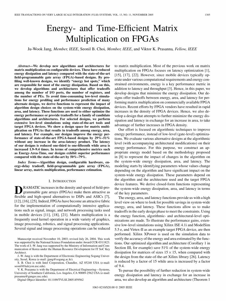
Fig. 1. Energy distribution of the design proposed in [22].
Kumar and Tsai [22] achieved the theoretical lower bound forlatency for matrix multiplication with a linear systolic design.They provide tradeoffs between the number of registers and thelatency. Their work focused on reducing the leading coefficientfor the time complexity. Our work focuses on minimizing en-ergy dissipation under constraints for area and latency. We sig-nificantly reduce the number of registers involved in the move-ment of intermediate results and elements of input matrices.
, registers of 8-b words are involved inthe data movement for matrix multiplication in [22]. In ourdesign, only registers of 8-b words are involved in the sys-tolic data movement (based on Theorem 1). Extra registersof 8-b words are required to store copies and are not involved inthe systolic data movement. Their work is not implemented onFPGAs.
The most appropriate reference design with which the perfor-mance of our designs should be compared comes from Xilinx[26]. The state-of-the-art design from Xilinx library performsmatrix multiplications for limited sizes (3 3). Xilinx XPower[26] can be used to measure the power dissipation of designs im-plemented on Xilinx FPGA devices. For a fair comparison, weuse the same design environment, the same target device, andthe same power measurement tool. Details of the simulationscan be found in Section VI. Xilinx just provides a point designoptimized at the gate level. Our work constructs a design spacespanned by possible design choices in our algorithm.
III. ENERGY-EFFICIENT ALGORITHMS/ARCHITECTURES FOR
MATRIX MULTIPLICATION
For performance comparison purposes, we have implementedthe latency-optimal systolic design [22] on FPGA devices. Theenergy distribution profile of the design reveals that much ofthe total energy is dissipated in the registers (see Fig. 1). Forexample, 78% of the energy is used in the registers for 12 12matrix multiplication.
By identifying the energy hot spot, we propose new energy-efficient algorithms and architectures for matrix multiplication.We present our algorithms and architectures in two theoremsand two corollaries. Pseudocode for cycle-specific data move-ment, the detailed architectures, and a snapshot of an examplecomputation are also shown. Theorem 1 improves the latency-optimal algorithm for matrix multiplication [22] in terms of thenumber of registers used in the designs. Our design has optimal
JANG et al.: ENERGY- AND TIME-EFFICIENT MATRIX MULTIPLICATION ON FPGAs 1307
Fig. 2. (a) Off-chip design and (b) on-chip design. (c) Architecture of PE used in Theorem 1. (d) Algorithm used in Theorem 1.
time complexity with a leading coefficient of 1 for matrix mul-tiplication on a linear array. Theorem is extended to Corollary 1for tradeoffs among energy dissipation, area, and latency. Corol-lary 1 is used to identify energy-efficient designs under latencyand area constraints.
The second algorithm is developed to exploit further in-creases in the density of FPGA devices to realize improvementsin energy dissipation and latency (Theorem 2). It uses moreMACs and I/O ports. Corollary 1 and Theorem 2 are integratedinto Corollary 2. Corollary 2 provides more comprehensivetradeoffs among energy dissipation, area and latency thanCorollary 1.
Based on the location of the input and output matrices, wehave two design scenarios: off-chip design and on-chip design[see Fig. 2(a) and (b)]. In the off-chip design, we assume thatthe input matrices are stored outside the FPGA. I/O ports areused for data access. While we assume that the input matricesare stored in an external memory outside the FPGAs, we do notinclude the energy used by the external memory. However, inthe on-chip design, we store all input and output matrices inan on-chip memory of the FPGA devices. The on-chip memoryrefers to an embedded memory in FPGAs. For example, a BlockSelectRAM in the Xilinx Virtex-II devices can be used for theon-chip memory. Thus, the energy used by the on-chip memoryis included in the on-chip design.
Theorem 1: matrix multiplication can be performedin cycles using 3 I/O ports and processing elements(PEs), each having a MAC (MAC-and-accumulator), 4 registers,and 2 local memories of words (Fig. 2(a) and (b) shows alinear array connecting the PEs and Fig. 2(c) shows a PE).
Proof: The algorithm in Fig. 2(d) and the architecture inFig. 2(a)–(c) are devised to computefor all and represent elements of thematrices and . denotes the th PE from the left inFig. 2(a), . computes\column of matrix
, which is stored in the local memory Cbuf.In Phase column of matrix and row ofmatrix traversein order and allow to update , where
represents the intermediate value of . Once arrivesat , a copy of resides in until
pass through . We observe that the following two essentialrequirements should be satisfied: 1) since stays at eachfor just one cycle, should arrive at no later than ,for any and 2) once arrives at , a copy of
should reside in until arrives. We show how thesetwo essential requirements for our systolic implementation aresatisfied with a minimal number of registers. In addition, weevaluate the number of cycles required to finish the operationand the amount of local memory per PE. An illustrative snapshotfor is provided for more clarity.
1) should arrive at no later than , for any: matrix is fed to the lower I/O
port of [see Fig. 2(c)] in row major order. Matrix is fed
to the upper I/O port of in column major ordercycles behind
matrix . For example, is fed to the upper I/O port ofin the same cycle as is fed to the lower I/O port
of . The number of cycles required for to arrive atis . requires
cycles to arrive at . The requirement is satisfied sincefor
all and . For example, we show how (the lastelement of matrix in phase 2) arrives at no laterthan (the first element of matrix in phase 2) for
. needs cycles.needs cycles.
2) Once arrives at a copy of should residein until arrives: we show how to minimize thenumber of registers to store copies ofin for each . We prove that two registers [denotedBM and BL in Fig. 2(c)] are sufficient to hold at(to store two consecutive elements, and ). Forexample, when arrives at is in BL and isin BM. If we can prove that has arrived atcan replace in BL. Note that is no longer neededin after is performed using
. In general, is needed until arrives at inthe -th cycle. ar-rives at in the th cycle. Since
for all
1308 IEEE TRANSACTIONS ON VERY LARGE SCALE INTEGRATION (VLSI) SYSTEMS, VOL. 13, NO. 11, NOVEMBER 2005
Fig. 3. Snapshot of the data flow for 3� 3 matrix multiplication (Theorem 1).
, and can be replaced when arrives at. Also, the time difference between and is
,which has a minimum value of 1. Hence, in the worstcase, arrives one cycle after is no longer re-quired, which means that can replace . Thisalso shows that cannot arrive while is usedsince barely arrives after is no longer required.This proves that needs at least two temporary regis-ters, BM and BL, to hold .
3) cycles are needed to complete the matrix mul-tiplication. The computation finishes one cycle afterarrives at , which is the -thor th cycle.
4) On completion of the above matrix multiplication, columnof the resulting output matrix is in Cbuf of , for
. To move the matrix out of the array, weuse an extra local memory CObuf and two ports Coutand Cin in each PE. Once column of the resultingoutput matrix is available in the Cbuf of , it ismoved to CObuf of for . Column 1 ismoved out of the array via Cout of . Columns 2 toare moved out of the array in a pipelined fashion throughCObufs of to . Using CObuf, the moving ofthe output matrix for the current matrix multiplicationout of the array can be overlapped with the next matrixmultiplication involving Cbuf. Without the overlapping,it takes extra cycles to move the resulting outputmatrix out of the array. Note that the first element of theoutput matrix, is available after -th cycle and ittakes cycles to move the rest of the output matrixout of the array.
A snapshot of the execution of the algorithm is provided forin Fig. 3. It shows the contents of the registers, A, BU, BM,
andBL of each PE during each cycle of the matrix multiplicationprocess. For example, , and stay in duringcycle 6. and (in the dark circles) are used to update
. Note that is no longer needed after thisupdate and hence can be replaced by , which arrives in cycle7. Elements of matrix stay in register A for one clock cycleand pass through while elements of matrix are prefetched intoregisters, BU, BM, and BL of each PE in the linear array and stayuntil they are no longer needed.
Corollary 1: matrix multiplication can be performed incycles using three I/O ports and PEs, each
having one MAC, two local memories of words, and fourregisters, where is divisible by .
Proof: matrix multiplication can be decomposedinto matrix multiplications, assuming that isdivisible by . Using Theorem 1 with replaced by , theproof follows.
Corollary 1 provides tradeoffs between area and latency.Larger values for reduces the number of PEs, which resultsin less area. However, it increases the number of cycles tocomplete the matrix multiplication. Combined with power andarea estimation of modules, Corollary 1 provides tradeoffsamong energy dissipation, area, and latency.
Theorem 2: matrix multiplication can be performed incycles using 3 I/O ports and PEs, each
having MACs, local memories of words, andregisters [Fig. 4(a) shows a PE for ], where is divisibleby .
A detailed proof is provided in the Appendix. Here, we showonly the basic idea. Corollary 1 decomposes a matrix mul-tiplication into matrix multiplications and per-forms them in a serial manner to reduce the area with increasedlatency. Theorem 2 performs the matrix mul-tiplications in a parallel manner to reduce the latency with in-
JANG et al.: ENERGY- AND TIME-EFFICIENT MATRIX MULTIPLICATION ON FPGAs 1309
Fig. 4. (a) Architecture of PE . (b) Algorithm for Theorem 2.
creased area. A direct application of Theorem 1 to reduce thelatency by the factor of would increase the resource times.This means I/O ports and PEs with MACs, reg-isters, and local memories of words per PE. We devisea new data movement scheme to reduce the number of registersand I/O ports by the factor of , saving greatly the area and theenergy consumption. Once a submatrix of size
from or is loaded, it is shared by the MACs instead if aMAC during its stay in each PE without any increase in latency.The registers consume a considerable amount of energy due tofrequent switching of intermediate results. Besides, we overlapthe input of two subsequent submatrices to reduce the latencyfrom to cycles. Fig. 4(a) showsour architecture for and Fig. 4(b) shows the accompa-nying algorithm. Refer to the Appendix for more details.
Corollary 1 and Theorem 2 combined together widen thedesign space where the tradeoff among area, latency, and en-ergy dissipation is possible. It must be noted that the number ofMACs is a key parameter to determine the whole architecture.Based on the number of MACs, Theorem 2 and Corollary 1 canbe combined into Corollary 2.
Corollary 2: matrix multiplication can be performedin cyclesusing MACs, 2 local memories ofwords, registers, and I/O ports,where is divisible by and .
Proof: For , the proof follows from Corollary1 by setting . For , the proof followsfrom Theorem 2 by setting .
Smaller values for reduce the number of modules such asMACs, registers, and I/O ports used in the design, resulting ina lesser area but the latency is seen to increase. Combined withthe latency of a design and the area and the power dissipationof the modules, Corollary 2 provides tradeoffs among energydissipation, area, and latency for . Corollary 2provides a more comprehensive set of tradeoffs than Corollary1 or Theorem 2 since the number of MACs used varies within awide range for a given problem size . Note that Corollary 1 andTheorem 2 provide tradeoffs among energy dissipation, area,and latency for and , respectively, andhence can be viewed as subsets of Corollary 2. A more detailedanalysis of all designs with respect to energy, area, and latencyis presented in Section IV-C.
IV. PERFORMANCE MODELING AND OPTIMIZATION
Given the goal of algorithmic-level optimization of energyperformance for matrix multiplication on FPGA devices, weneed an energy model to represent the impact of individual al-gorithmic-level choices on the energy performance. Based onthis model, we make the design tradeoffs to obtain energy-ef-ficient designs. The candidate designs are implemented in Sec-tion V-A.
A. Domain-Specific Energy Model
Our approach for the performance modeling is to use a do-main-specific energy model [8]. The model is applicable onlyto the design domain spanned by the family of algorithms andarchitectures being evaluated. The family represents a set of al-gorithm-architecture pairs that exhibit a common structure andsimilar data movement. The domain is a set of point designsresulting from unique combinations of algorithm- and architec-ture-level changes. The domain-specific energy model abstractsthe energy dissipation to suit the design domain. The abstrac-tion is independent of the commonly used levels such as gate,
1310 IEEE TRANSACTIONS ON VERY LARGE SCALE INTEGRATION (VLSI) SYSTEMS, VOL. 13, NO. 11, NOVEMBER 2005
register, or system level. Rather, it is based on the knowledgeof the family of algorithms and architectures. The parametersare extracted considering their expected impact on the total en-ergy performance. For example, if the number of MACs and thenumber of registers change values in a domain and are expectedto be frequently accessed, a domain-specific energy model isbuilt using them as key parameters. The parameters may includeelements at the gate, register, or system level as needed by thedomain. It is a knowledge-based model that exploits the knowl-edge of the designer about the algorithm and the architecture.
We also use the knowledge to derive functions that representenergy dissipation, area, and latency. Beyond the simple com-plexity analysis, we make the functions as accurate as possibleby incorporating implementation and target device details. Forexample, if the number of MACs is a key parameter, we imple-ment a sample MAC on the target FPGA device to estimate itsaverage power dissipation. Random input vectors, as many asare needed for the desired confidence interval [13], are gener-ated for simulation. A power function representing the powerdissipation as a function of , the number of MACs, is gener-ated. This power function is obtained for each module relatedto the key parameters. Based on the designer’s optimizationgoal and the time available for design, a balance needs to bestruck between accuracy and simple representation of the func-tions. The estimation error of the functions derived in this paperranges from 3.3% to 7.4%. Since the model is intended for algo-rithmic-level analysis in the early stage of the design, the erroris considered satisfactory.
Our family of architectures and algorithms for matrixmultiplication forms a domain and we limit algorithm-levelexploration for energy optimization to the design space spannedby this domain. The family of architectures and algorithms inFigs. 2 and 4, and the parameters in Table I represent the designspace. We build two domains for Corollary 1 and Theorem 2.Two parameters, and , are used. In Corollary 1, denotes thesize of input matrices. is introduced for block multiplicationusing submatrices of size . In Theorem 2, determinesthe number of I/O ports , the number of MACs , and thesubmatrices of size . Due to the nature of our algorithms,the number of each key module depends only on these twoparameters.
We identify registers of 8-b and 16-b words, MACs, SRAMs(distributed SelectRAMs in the Xilinx devices), and BSRAMs(Block SelectRAMs in the Xilinx Virtex-II devices) [26] as keymodules. Choosing specific values for the parameters in Table Iresults in a design point in the design space. For example,
, andrepresents a design where 24 24 matrix multiplication is
implemented using six PEs with four registers, one MAC, andtwo SRAMs per PE. The input and output matrices are stored intwo BSRAMs on the device and noI/O ports are used.
An energy model specific to the domain is constructed at themodule level by assuming that each module of a given type(register, multiplier, SRAM, BSRAM, or I/O port) dissipatesthe same power independent of its location on the chip. Thismodel simplifies the derivation of system-wide energy dissipa-tion functions. The energy dissipation for each module can be
TABLE IRANGE OF PARAMETERS FOR XILINX XC2V1500
determined by counting the number of cycles the module staysin each power state and low-level estimation of the power usedby the module in the power state, assuming average switchingactivity. Additional details of the model can be found in [8].
Table II lists the key parameters and the number of each keymodule in terms of the two parameters for each domain. In addi-tion, it shows the latencies which also depend on the parameters.By choosing specific values for the parameters in Table II, a dif-ferent design is realized in the design space. For example, a de-sign with and represents a design where 16 16matrix multiplication is implemented using four PEs with fourregisters, one MAC, and one SRAM per PE.
B. Functions to Estimate Energy, Area, and Latency
Functions that represent the energy dissipation, area, and la-tency are derived for Corollary 1 and Theorem 2. The energyfunction of a design is approximated to be , whereand represent the number of active cycles and average powerfor module . For example, denotes the average powerdissipation of the multiplier module. The average power is ob-tained from low-level power simulation of the module. The areafunction is given by , where represents the area usedby module . In general, these simplified energy and area func-tions may not be able to capture all of the implementation detailsneeded for accurate estimation. However, we are concerned withalgorithmic-level comparisons, rather than accurate estimation.Moreover, our architectures are simple and have regular inter-connections, and so the error between these functions and theactual values based on low-level simulation is expected to besmall. In Section V-B, we evaluate the accuracy of the energyand area functions. The latency functions is obtained easily be-cause the theorems and corollaries already give us the latencyin clock cycles for the different designs.
Table II shows the number of modules used by the designs formatrix multiplication with 8-b input precision and 16-b
output precision. For the off-chip design, I/O ports are used tofetch elements from outside the FPGA. In the on-chip design,BSRAMs of 1024 16-b words are used for on-chip storage ofinput matrices. SRAMs are CLB-based memory blocks usedfor storing intermediate results. The power and area values of
JANG et al.: ENERGY- AND TIME-EFFICIENT MATRIX MULTIPLICATION ON FPGAs 1311
TABLE IINUMBER OF MODULES USED AND THE LATENCY OF VARIOUS DESIGNS
TABLE IIIENERGY AND TIME PERFORMANCE MODELS
each module are shown in Table IV. For example, isthe average power used by SRAM (16-b word), where is thenumber of entries. In the actual implementation of a SRAM, thenumber of its entries should be multiples of 16. denotesthe remaining power dissipation of a PE (after the modules havebeen accounted for), and takes care of glue logic and controllogic. Similar numbers representing the area of each moduleare also obtained. denotes the area of a PE that accountsfor glue logic and control logic. The latencies are obtained interms of seconds by dividing them by the clock frequency. UsingTable II, functions that represent energy, area, and latency forCorollary 1 and Theorem 2 are shown in Table III. Functionsfor other designs can be obtained in the same way. An averageswitching activity of 50% for input data to each module at arunning frequency of 150 MHz is assumed. Multiply operationis performed using dedicated embedded multipliers available inthe Virtex-II device.
Note that throughput is important, since many applicationsfor matrix multiplication process a stream of data. Our designin Corollary 1 is a pipelined architecture, with the first cy-cles of the computations on the next set of data being overlapped
TABLE IVPOWER AND AREA FUNCTIONS FOR VARIOUS MODULES
with the last cycles of the computations on the current setof data. Thus for a stream of matrices, an sub-matrix can be processed every cycles. Thus, the effec-tive latency becomes , which is the time between the ar-rivals of the first and last output data of the current computation.Hence, the design in Corollary 1 is a throughput-oriented designsince one output is available every clock cycle for a stream of
1312 IEEE TRANSACTIONS ON VERY LARGE SCALE INTEGRATION (VLSI) SYSTEMS, VOL. 13, NO. 11, NOVEMBER 2005
Fig. 5. Energy, area, and latency tradeoffs of Corollary 1 as a function of the block size (n=r). (a) Off-chip and (b) on-chip design for n = 48.
matrices. The design in Theorem 2 is also throughput-orientedsince output data items are available every clock cycle. Its ef-fective latency becomes .
C. Tradeoffs Among Energy, Area, and Latency
The functions in Table III are used to identify tradeoffsamong energy, area, and latency. For example, Fig. 5 illustratesthe tradeoffs among energy, area, and latency for 48 48matrix multiplication for the off-chip and on-chip designs ofCorollary 1. It can be used to choose energy-efficient designsto meet given area and latency constraints. For example, if 800slices are available and the latency should be less than 6000cycles (36 s), an energy-efficient design is obtained using
. The energy dissipation, area, and latency for such adesign, evaluated using the functions in Table III, are 6.85 J,524 slices, and 5400 cycles (32.4 s), respectively. Fig. 5 showsthat, as the block size increases, the area increases and thelatency decreases, because the degree of parallelism increases.While the energy dissipation decreases to or ,it starts increasing afterwards. The reason for this behavior isas follows. The energy used by the local storages, Cbuf andCObuf, is and is hence pro-portional to . The energy used by the rest of modules,except I/O, are proportional to . The energy for I/O isproportional to . As increases ( decreases), theenergy used by I/O decreases relatively faster, and thus the total
energy decreases. However, after , the energy usedby the local storage becomes the dominant factor. This helpsus to identify the optimal block size for energy-efficient matrixmultiplication.
Tradeoff analysis for the on-chip model also shows similarbehavior. The on-chip design uses BSRAMs instead of I/Oports. Since the energy used in I/O ports is more than the energyused in the BSRAMs, the energy used in the on-chip design isless than the energy used in the off-chip design. However, thechoice between the off-chip and on-chip design depends on thesituation—whether the matrix multiplication is stand-alone ora part of an application (e.g., an application consists of multiplekernels).
Theorem 2 provides asymptotic improvement in energyand latency performance in the on-chip model. As shown inTable II, asymptotically, the energy dissipated in the BSRAMsand the latency of the Xilinx reference design increase as
and , respectively, assuming a unit of energy isused per cycle for retaining a word in the BSRAM. Energydissipation and latency for the designs based on Theorem 1and [22] increase as and , respectively, under thesame assumptions. Theorem 2 improves these complexitiesto and , respectively, where is theblock size for block multiplication and is divisible by with
. Further increases in the density of FPGAs can be usedto increase the number of multipliers and hence , leading toasymptotic reduction in energy dissipation and latency.
JANG et al.: ENERGY- AND TIME-EFFICIENT MATRIX MULTIPLICATION ON FPGAs 1313
Fig. 6. Energy, area, and latency tradeoffs of Theorem 2 as a function of r. (a) Off-chip and (b) on-chip design for n = 48.
Fig. 6 shows the tradeoffs among energy, area, and latencyfor Theorem 2. As the value of increases (or block sizedecreases), the area increases and the latency decreases. How-ever, the energy dissipation continuously decreases. Thus, thedesigns based on Theorem 2 reach the minimal point of energydissipation when the block size is the smallest unlike the de-signs based on Corollary 1. Note that the local storages consistsof registers, Cbufs, and CObufs. The energy used by the reg-isters in the designs based on Theorem 2 is while theenergy used by the registers in the designs based on Corollary1 is for the same problem size. Thus, the energy used bythe registers in the designs based on Theorem 2 decreases asincreases while the energy used by the registers in the designsbased on Corollary 1 is constant. The same analysis applies tothe energy complexity of BSRAMs.
D. Other Optimization Techniques for Energy Efficiency
To optimize the energy performance of our design, we em-ploy several energy-efficient design techniques [9]. One suchtechnique is architecture selection. FPGAs give the designerthe freedom to map almost any architecture onto hardware. Dif-ferent architectures have varying energy performances, laten-cies, and throughputs. In our design, we have chosen a lineararray of processing elements. In FPGAs, long interconnects dis-sipate a significant amount of power [24]. Therefore, for en-ergy-efficient designs, it is beneficial to minimize the number oflong interconnects. A linear array of PEs accomplishes this goal.
Each processing element communicates only with its nearestneighbors, minimizing the use of long wires. Additionally, thelinear array architecture facilitates the use of two more tech-niques: parallel processing and pipelining. Both parallel pro-cessing and pipelining decrease the effective latency of a de-sign. Parallel processing does so by increasing the amount ofresources while pipelining does so by increasing the resourceutilization. By decreasing effective latency, both techniques canlead to lower energy dissipation. However, these techniques canalso increase the power dissipation, which can have a nega-tive effect on the energy dissipation. The designer must reacha compromise between low latency and high power in order toachieve a low-energy design. Another technique that we employis the choosing of the appropriate bindings. In an FPGA, therecan be many possible mappings of the computation and storageelements to the actual hardware. For example, in the XilinxVirtex-II, the storage Cbuf can be implemented as registers, adistributed SelectRAM, or a Block SelectRAM. Each of thesetypes of storage dissipates a different amount of energy and canlead to implementations with wide variation in energy dissipa-tion. When the number of entries , a Block SelectRAM isused since it is energy-efficient as a large memory; otherwise, adistributed SelectRAM is used. Similar decisions can be madefor other elements of the design, such as choosing multiplicationunit. The architecture of the target Virtex-II FPGA offers twooptions to implement a multiplier: 1) Block Multiplier, whichis an ASIC-based embedded multiplier and 2) slices to build a
1314 IEEE TRANSACTIONS ON VERY LARGE SCALE INTEGRATION (VLSI) SYSTEMS, VOL. 13, NO. 11, NOVEMBER 2005
Fig. 7. (a) Pipelining stages. (b) Data hazard.
configured multiplier. By default, the Xilinx ISE XST tool usesthe Block Multiplier for multiplication. In our designs, all of themultiplications are performed using the Block Multipliers sincethey are energy-efficient when any of the inputs is not constant.
V. DESIGN SYNTHESIS AND SIMULATION
Based on the high-level performance estimation, the chosendesigns are implemented and simulated to obtain the accurateresults. Our target device is Xilinx Virtex-II which is a high-performance platform FPGA from Xilinx [26]. We have chosenthe XC2V1500 and XC2V3000 models with a 5 speed gradefor comparison. These models have 48 and 96 18 18-b BlockMultipliers, respectively.
A. Implementation Details
Based on the observation in Section IV-C, we implementedthe designs using VHDL in the Xilinx ISE 4.1i environment.All parameters are specified using “Generic” variables inVHDL syntax. By changing the values of the Generic vari-ables, different numbers and types of modules are instantiated(see Table II), and eventually the whole architecture is syn-thesized accordingly. Note that the design for Theorem 1 hasone parameter , and Corollary 1 and Theorem 2 have twoparameters and . These are only necessary parameters fordesign synthesis. For the off-chip design, all matrix data arefed via I/O ports. Thus, the total energy includes the energyused for I/O. For the on-chip design, the data are stored inthe BSRAMs first and fed into the first PE from the BSRAM.However, the energy used to store the data in BSRAM via I/Oports is not included unlike the case of the off-chip design.
The whole design as well as the design for a PE are pipelined.Fig. 7(a) shows the pipeline stages of each PE and Fig. 7(b)shows the pipelining in each PE. Cbuf is implemented usinga dual-port SRAM. Note that there is data feedback which isrequired for accumulation of intermediate values for matrix C.To accumulate the intermediate values, one data comes fromthe MAC and the other one comes from Cbuf. If , thememory read for intermediate value occurs after the value iswritten to Cbuf. However, if for Theorem 1 or
for Theorem 2, data hazard occurs. Since two clock cycles
are required between the memory write and read, the distancebetween read-after-writes (RAWs) has to be two clock cycles toprevent the data hazard.
Other than the data paths for all designs, control logic is alsoparameterized based on and . The first approach for con-trol logic is that one centralized control logic generator providesmost of the control signals for the first PE and then the rest ofthe PEs receive the delayed control signals from their respec-tive previous PEs. Since all PEs perform the same operations ina systolic manner, the delayed control signals are well suited inour design. Another approach is to have one control logic gen-erator in each PE, which means that distributed control logicgenerators are used. In both approaches, the control logic gen-erator consists of simple counters and combinational logic. Thecentralized control logic uses less area but more interconnectscompared with the distributed control logic. In our design, thedifference in the energy dissipation of two approaches is negli-gible. Thus, we choose the mixture of distributed and central-ized controls in our designs. Each PE of the off-chip design forTheorem 1 and Theorem 2 has 6 control signals from the controllogic (i.e., centralized control). The centralized control signalsare generated from the control logic (outside PE) and are fedto the first PE. Note that only the first PE gets the control sig-nals and the rest of PEs use them in a pipelining manner [seeFig. 2(a) and (b)]. Then, all signals are passed to the next PEwith one or two clock delays. Address generation for Cbuf andCObuf are generated inside PE in a distributed manner. The firstcontrol signal CtRegLoad is used to load the input data to BMor BL. It is asserted every cycles (see Fig. 3). CtMuxTo-Mult is used to determine which BM or BL is multiplied withA. This signal is identical to CtRegLoad except for the first
cycles. CtMultCe and CtRamWe are the enable signalsfor the multiplier and SRAM. Both are asserted when the com-putation starts. CtFlush is asserted after one set computationfor matrix multiplication is completed and a newset of computation starts. Cbuf needs to be flushed before thenext result is stored. It is asserted at andis on for cycles and is off for cycles.In the data path, using this signal, we accumulate the interme-diate values for matrix with previous intermediate values or0 (flushing effect). CtCoutMux is used to determine whetherthe results come from an accumulator or CObuf. It triggers thedata pulling from the current CObuf to the previous PE. In fact,the current PE sends the data of CObuf to the previous PE. Itis asserted at and is on for cycles and is offfor cycles. For the on-chip design, the controllogic includes the additional signals such as address generationfor on-chip memory. In addition, the energy used by the controllogic is separately measured and accounts for about 10% of thedesigns.
B. Simulation Method
Using the high-level model defined in Section IV-B, severaldesigns can be obtained by optimizing on latency, area, orenergy. In this paper, we attempt to arrive at minimal energy de-signs. The candidate designs are implemented in VHDL. Thesedesigns are synthesized using Xilinx Synthesis Technology(XST) in Xilinx ISE 4.1i. The place-and-route file (.ncd file) is
JANG et al.: ENERGY- AND TIME-EFFICIENT MATRIX MULTIPLICATION ON FPGAs 1315
TABLE VPERFORMANCE COMPARISON OF VARIOUS OFF-CHIP DESIGNS AGAINST
THE XILINX DESIGN
obtained for Virtex-II XC2V1500 and XC2V3000 (speed grade5). The input test vectors for the simulation are randomly
generated such that their average switching activity is 50%.ModelSim 5.6 b, from Mentor Graphics, is used to simulate thedesigns and generate simulation results (.vcd file). These twofiles are then provided to the Xilinx XPower tool to evaluatethe average power dissipation. Energy dissipation is furtherobtained by multiplying the average power with the effectivelatency.
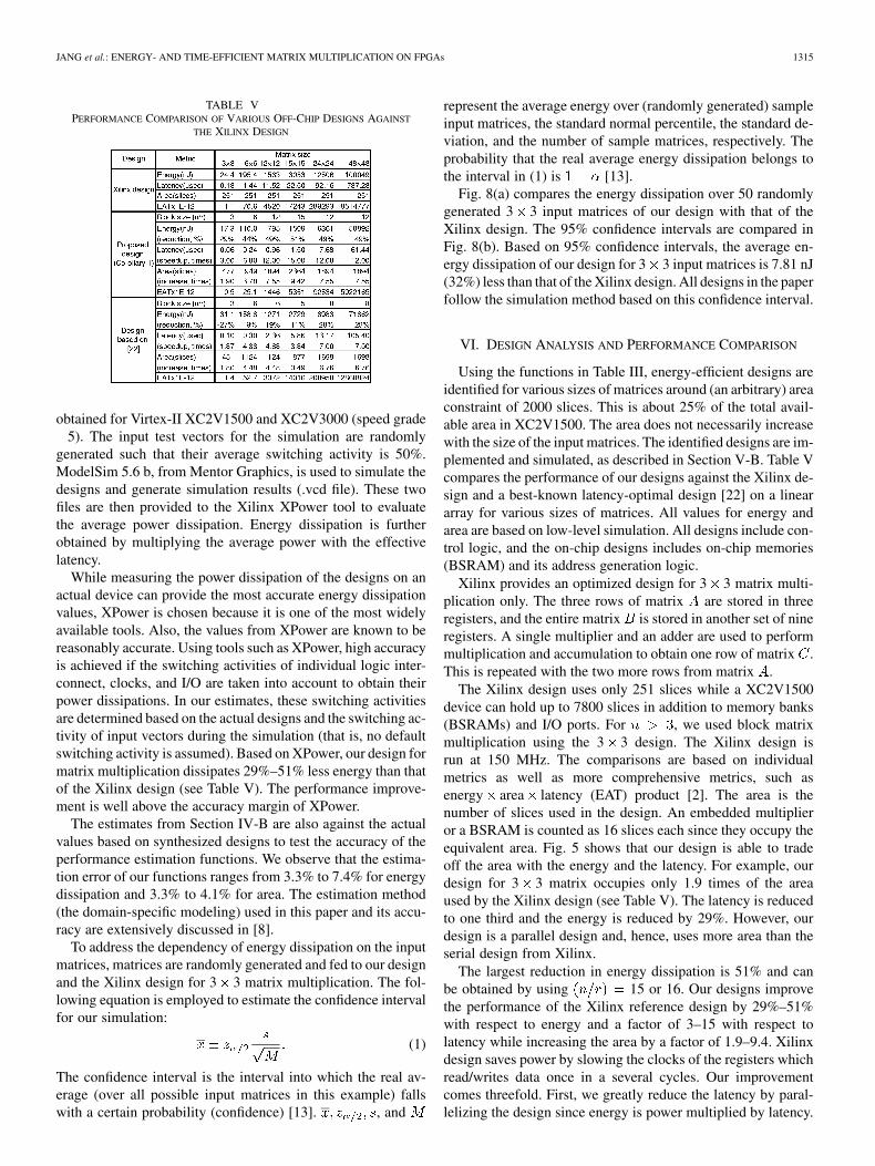
While measuring the power dissipation of the designs on anactual device can provide the most accurate energy dissipationvalues, XPower is chosen because it is one of the most widelyavailable tools. Also, the values from XPower are known to bereasonably accurate. Using tools such as XPower, high accuracyis achieved if the switching activities of individual logic inter-connect, clocks, and I/O are taken into account to obtain theirpower dissipations. In our estimates, these switching activitiesare determined based on the actual designs and the switching ac-tivity of input vectors during the simulation (that is, no defaultswitching activity is assumed). Based on XPower, our design formatrix multiplication dissipates 29%–51% less energy than thatof the Xilinx design (see Table V). The performance improve-ment is well above the accuracy margin of XPower.
The estimates from Section IV-B are also against the actualvalues based on synthesized designs to test the accuracy of theperformance estimation functions. We observe that the estima-tion error of our functions ranges from 3.3% to 7.4% for energydissipation and 3.3% to 4.1% for area. The estimation method(the domain-specific modeling) used in this paper and its accu-racy are extensively discussed in [8].
To address the dependency of energy dissipation on the inputmatrices, matrices are randomly generated and fed to our designand the Xilinx design for 3 3 matrix multiplication. The fol-lowing equation is employed to estimate the confidence intervalfor our simulation:
(1)
The confidence interval is the interval into which the real av-erage (over all possible input matrices in this example) fallswith a certain probability (confidence) [13]. , and
represent the average energy over (randomly generated) sampleinput matrices, the standard normal percentile, the standard de-viation, and the number of sample matrices, respectively. Theprobability that the real average energy dissipation belongs tothe interval in (1) is [13].
Fig. 8(a) compares the energy dissipation over 50 randomlygenerated 3 3 input matrices of our design with that of theXilinx design. The 95% confidence intervals are compared inFig. 8(b). Based on 95% confidence intervals, the average en-ergy dissipation of our design for 3 3 input matrices is 7.81 nJ(32%) less than that of the Xilinx design. All designs in the paperfollow the simulation method based on this confidence interval.
VI. DESIGN ANALYSIS AND PERFORMANCE COMPARISON
Using the functions in Table III, energy-efficient designs areidentified for various sizes of matrices around (an arbitrary) areaconstraint of 2000 slices. This is about 25% of the total avail-able area in XC2V1500. The area does not necessarily increasewith the size of the input matrices. The identified designs are im-plemented and simulated, as described in Section V-B. Table Vcompares the performance of our designs against the Xilinx de-sign and a best-known latency-optimal design [22] on a lineararray for various sizes of matrices. All values for energy andarea are based on low-level simulation. All designs include con-trol logic, and the on-chip designs includes on-chip memories(BSRAM) and its address generation logic.
Xilinx provides an optimized design for 3 3 matrix multi-plication only. The three rows of matrix are stored in threeregisters, and the entire matrix is stored in another set of nineregisters. A single multiplier and an adder are used to performmultiplication and accumulation to obtain one row of matrix .This is repeated with the two more rows from matrix .
The Xilinx design uses only 251 slices while a XC2V1500device can hold up to 7800 slices in addition to memory banks(BSRAMs) and I/O ports. For , we used block matrixmultiplication using the 3 3 design. The Xilinx design isrun at 150 MHz. The comparisons are based on individualmetrics as well as more comprehensive metrics, such asenergy area latency (EAT) product [2]. The area is thenumber of slices used in the design. An embedded multiplieror a BSRAM is counted as 16 slices each since they occupy theequivalent area. Fig. 5 shows that our design is able to tradeoff the area with the energy and the latency. For example, ourdesign for 3 3 matrix occupies only 1.9 times of the areaused by the Xilinx design (see Table V). The latency is reducedto one third and the energy is reduced by 29%. However, ourdesign is a parallel design and, hence, uses more area than theserial design from Xilinx.
The largest reduction in energy dissipation is 51% and canbe obtained by using 15 or 16. Our designs improvethe performance of the Xilinx reference design by 29%–51%with respect to energy and a factor of 3–15 with respect tolatency while increasing the area by a factor of 1.9–9.4. Xilinxdesign saves power by slowing the clocks of the registers whichread/writes data once in a several cycles. Our improvementcomes threefold. First, we greatly reduce the latency by paral-lelizing the design since energy is power multiplied by latency.
1316 IEEE TRANSACTIONS ON VERY LARGE SCALE INTEGRATION (VLSI) SYSTEMS, VOL. 13, NO. 11, NOVEMBER 2005
Fig. 8. Comparison between our design (based on Theorem 1) and Xilinx design for 3� 3 matrix multiplication. (a) Energy dissipation for randomly generatedmatrices. (b) Average energy dissipation with confidence intervals.
TABLE VIPERFORMANCE COMPARISON OF VARIOUS ON-CHIP DESIGNS
Second, we reduce the amount of switching by reducing thenumber of registers on the systolic path. Third, we use theprediction functions to choose the most promising design in thedomain-specific design space.
The designs based on [22] with the same latency as ours re-duce the energy dissipation by 27%–31% when compared withthe Xilinx design. Analysis of energy and area functions re-veals that the performance improvement of our designs over theXilinx design due to the reduction in latency and energy-effi-cient binding. In terms of energy–area–time (EAT), our designsbased on Corollary 1 offer superior performance by 50%–79%compared with the Xilinx design.
The latency of our design ranges from 1/3-1/15 of the Xilinxdesign, resulting in less energy consumption. The leakage en-ergy (leakage power latency) is proportional to the productof area and latency. The area–latency product of our design issmaller than that of the Xilinx designs, and thus leakage energyof our designs is smaller as compared to the Xilinx designs.
Table VI shows the energy, area, and latency of on-chip de-signs in Corollary 1 for various problem sizes. While the com-parison of off-chip and on-chip designs is not fair, it is usefulto analyze the effect of I/O ports and on-chip memory. For theoff-chip design, data are fed via the I/O ports of the FPGA. Thepower used by a 16-b I/O port is 80 mW. The input ports useless power than the output ports since the output ports need tohandle a large fan-out. For the on-chip design, all data are storedin BSRAMs. The power dissipation of the read and write oper-ations on a single-port BSRAM with 50% access rate is 35 mW.
Fig. 9. Energy distribution over logic, net, and I/O for Theorem 1 and 2.
Thus, data access from a BSRAM is more energy-efficient thanfrom an I/O port. However, we likely have a combination ofboth situations, where we read the data from input ports andstore the result in BSRAMs for further computation. The finalresult would be obtained after several computations and outputvia output ports. Thus, the design tradeoffs have to be performedat a system level where multiple kernels are integrated.
Fig. 9 shows the energy distribution among logic, net, and I/Oports for Theorems 1 and 2. The figures are based on the off-chipdesigns. Logic energy represents the energy used by the combi-national logic in the design. Net energy is the energy used byinterconnect wires, and I/O energy by input/output ports. Notethat the algorithm of Theorem 2 uses more energy in the netsthan in the logic, unlike Theorem 1. For example, the ratio of(logic energy)/(net energy) is 1.21 for Theorem 1 and 0.75 forTheorem 2. The reason is that Theorem 2 has a more complexdesign for a PE and uses more interconnects between PEs. Inthe low-level simulation, Theorem 1 runs at 150 MHz. How-ever, Theorem 2 runs at 143 MHz or less due to a more complexdesign involving more interconnect wires.
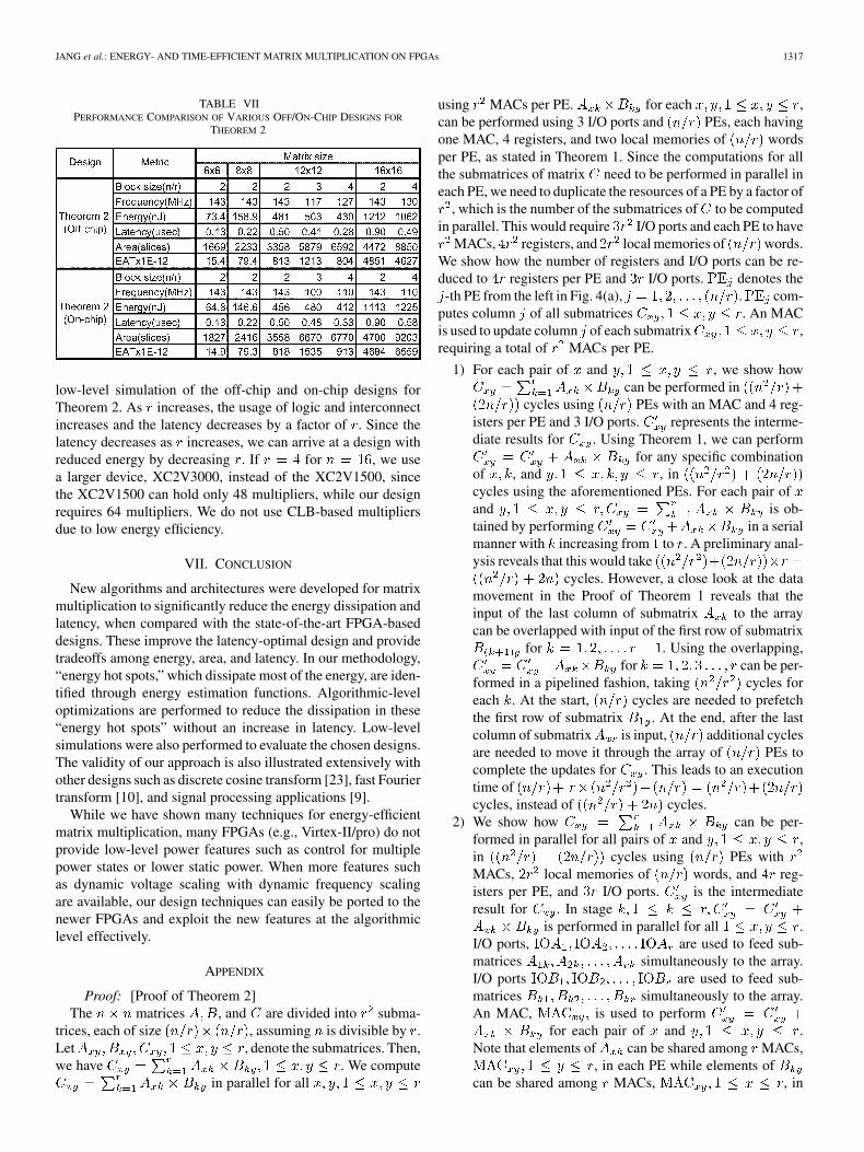
Another factor that affects the energy dissipation inTheorem 2 is the parameter, , which determines the de-gree of parallelism. Table VII shows the results from the
JANG et al.: ENERGY- AND TIME-EFFICIENT MATRIX MULTIPLICATION ON FPGAs 1317
TABLE VIIPERFORMANCE COMPARISON OF VARIOUS OFF/ON-CHIP DESIGNS FOR
THEOREM 2
low-level simulation of the off-chip and on-chip designs forTheorem 2. As increases, the usage of logic and interconnectincreases and the latency decreases by a factor of . Since thelatency decreases as increases, we can arrive at a design withreduced energy by decreasing . If for , we usea larger device, XC2V3000, instead of the XC2V1500, sincethe XC2V1500 can hold only 48 multipliers, while our designrequires 64 multipliers. We do not use CLB-based multipliersdue to low energy efficiency.
VII. CONCLUSION
New algorithms and architectures were developed for matrixmultiplication to significantly reduce the energy dissipation andlatency, when compared with the state-of-the-art FPGA-baseddesigns. These improve the latency-optimal design and providetradeoffs among energy, area, and latency. In our methodology,“energy hot spots,” which dissipate most of the energy, are iden-tified through energy estimation functions. Algorithmic-leveloptimizations are performed to reduce the dissipation in these“energy hot spots” without an increase in latency. Low-levelsimulations were also performed to evaluate the chosen designs.The validity of our approach is also illustrated extensively withother designs such as discrete cosine transform [23], fast Fouriertransform [10], and signal processing applications [9].
While we have shown many techniques for energy-efficientmatrix multiplication, many FPGAs (e.g., Virtex-II/pro) do notprovide low-level power features such as control for multiplepower states or lower static power. When more features suchas dynamic voltage scaling with dynamic frequency scalingare available, our design techniques can easily be ported to thenewer FPGAs and exploit the new features at the algorithmiclevel effectively.
APPENDIX
Proof: [Proof of Theorem 2]The matrices , and are divided into subma-
trices, each of size , assuming is divisible by .Let , denote the submatrices. Then,we have . We compute
in parallel for all
using MACs per PE. for each ,can be performed using 3 I/O ports and PEs, each havingone MAC, 4 registers, and two local memories of wordsper PE, as stated in Theorem 1. Since the computations for allthe submatrices of matrix need to be performed in parallel ineach PE, we need to duplicate the resources of a PE by a factor of
, which is the number of the submatrices of to be computedin parallel. This would require I/O ports and each PE to have
MACs, registers, and local memories of words.We show how the number of registers and I/O ports can be re-duced to registers per PE and I/O ports. denotes the-th PE from the left in Fig. 4(a), . com-
putes column of all submatrices . An MACis used to update column of each submatrix ,requiring a total of MACs per PE.
1) For each pair of and , we show howcan be performed in
cycles using PEs with an MAC and 4 reg-isters per PE and 3 I/O ports. represents the interme-diate results for . Using Theorem 1, we can perform
for any specific combinationof , and , incycles using the aforementioned PEs. For each pair ofand is ob-tained by performing in a serialmanner with increasing from to . A preliminary anal-ysis reveals that this would take
cycles. However, a close look at the datamovement in the Proof of Theorem 1 reveals that theinput of the last column of submatrix to the arraycan be overlapped with input of the first row of submatrix
for . Using the overlapping,for can be per-
formed in a pipelined fashion, taking cycles foreach . At the start, cycles are needed to prefetchthe first row of submatrix . At the end, after the lastcolumn of submatrix is input, additional cyclesare needed to move it through the array of PEs tocomplete the updates for . This leads to an executiontime ofcycles, instead of cycles.
2) We show how can be per-formed in parallel for all pairs of and ,in cycles using PEs withMACs, local memories of words, and reg-isters per PE, and I/O ports. is the intermediateresult for . In stage
is performed in parallel for all .I/O ports, are used to feed sub-matrices simultaneously to the array.I/O ports are used to feed sub-matrices simultaneously to the array.An MAC, is used to perform
for each pair of and .Note that elements of can be shared among MACs,
, in each PE while elements ofcan be shared among MACs, , in
1318 IEEE TRANSACTIONS ON VERY LARGE SCALE INTEGRATION (VLSI) SYSTEMS, VOL. 13, NO. 11, NOVEMBER 2005
each PE. For example, in any stage , allthe MACs, , in parallel perform
and need . This sharing al-lows us to reduce the number of registers required per PEfrom to and the number of I/O ports from to .A direct application of Theorem 1 without sharing woulduse 4 registers per PE and 3 I/O ports to feed each MAC,requiring registers per PE and I/O ports to thearray. Column of submatrix is updated byand stored in a local memory of size Cbuf , foreach , in .
3) One set of local memories (Cbufs) of words inis used to store intermediate results for column
of submatrix for any . Anotherset of local memories (CObufs) of words is re-quired to buffer the final results from to .Thus, a total of local memories of words perPE are required. Starting from the -th cycle,
results of are generated from all PEs during thenext cycles. CObuf is necessary in eachPE otherwise the final from one matrix multiplica-tion would be overwritten by the intermediate of thenext matrix. stores either the output from viaports or from of inCObufs. For the first cycles, the final at isoutput to via ports ports .For the next cycles, the stored ofin CObuf is output to . The outputs fromare the resulting matrix . Starting from the
-th cycle, stores the final of via portsin CObufs for cycles.
4) Fig. 4(a) shows our architecture for and Fig. 4(b)shows the accompanying algorithm. Let , and
, denote submatrices, each of size. In the first stage, , are
performed in parallel for all by feeding theelements of , and through the 4 inputports. In the second stage, isperformed in parallel for all . Each stagetakes cycles from Theorem 1. Since overlap-ping is possible between the end of the first phase and thestart of the second phase, the total number of cycles forboth stages combined is , as explained before.For larger values of , there is greater parallelism withinthe PEs and hence the execution time greatly reduces.
ACKNOWLEDGMENT
The authors wish to thank H. Krishnaswamy for helpful dis-cussions and comments on the earlier draft of this work. Theauthors would also like to thank J. Ou for editorial assistance.
REFERENCES
[1] A. Amira, A. Bouridane, and P. Milligan, “Accelerating matrix producton reconfigurable hardware for signal processing,” in Proc. 11th Int.Conf. Field-Programmable Logic and Its Applications (FPL), 2001, pp.101–111.
[2] B. Bass, “A low-power, high-performance, 1024-point FFT processor,”IEEE J. Solid-State Circuits, vol. 34, no. 3, pp. 380–387, Mar. 1999.
[3] J. Becker, T. Pionteck, and M. Glesner, “DReAM: A dynamically recon-figurable architecture for future mobile communication applications,” inProc. Field-Programmable Logic and Its Applications (FPL), 2002, pp.312–321.
[4] BenPRO Virtex TM-II Pro DIME-II Module [Online]. Available:http://www.nallatech.com/solutions/products/embedded_systems/dime2/rc_modules/benpro/
[5] A. Bogliolo, L. Benini, and G. Micheli, “Regression-based RTL powermodeling,” ACM Trans. Des. Automat. Electron. Syst., vol. 5, no. 3, pp.337–372, 2000.
[6] B. L. Bowerman and R. T. O’Connell, Linear Statistical Models—AnApplied Approach, 2nd ed. Pacific Grove, CA: Brooks/Cole, 1990.
[7] G. Brebner and N. Bergman, “Reconfigurable computing in remote andharsh environments,” in Proc. Field-Programmable Logic and Its Appli-cations (FPL), 1999, pp. 195–204.
[8] S. Choi, J.-W. Jang, S. Mohanty, and V. K. Prasanna, “Domain-specificmodeling for rapid energy estimation of reconfigurable architectures,” J.Supercomputing, vol. 26, no. 3, pp. 259–281, Nov. 2003.
[9] S. Choi, R. Scrofano, V. K. Prasanna, and J.-W. Jang, “Energy efficientsignal processing using FPGAs,” in Proc. Field Programmable GateArray (FPGA), 2003, pp. 225–234.
[10] S. Choi, G. Govindu, J.-W. Jang, and V. K. Prasanna, “Energy-efficientand parameterized designs of fast fourier transforms on FPGAs,” inProc. Int. Conf. Acoustics, Speech, and Signal Processing (ICASSP),vol. 2, 2003, pp. 521–524.
[11] O. D. Fidanci, D. Poznanovic, K. Gaj, T. El-Ghazawi, and N.Alexandridis, “Performance and overhead in a hybrid reconfigurablecomputer,” in Proc. Reconfigurable Architecture Workshop (RAW),2003, pp. 176–183.
[12] J. Frigo, M. Gokhale, and D. Lavenier, “Evaluation of the streams-CC-to-FPGA compiler: An applications perspective,” Proc. Field Pro-grammable Gate Arrays (FPGA), pp. 134–140, 2001.
[13] R. Hogg and E. Tanis, Probability and Statistical Inference, 6thed. Upper Saddle River, NJ: Prentice-Hall, 2001, pp. 656–657.
[14] J.-W. Jang, S. Choi, and V. K. Prasanna, “Energy efficient matrix mul-tiplication on FPGAs,” Proc. Field-Programmable Logic and Its Appli-cations (FPL), pp. 534–544, 2002.
[15] H. T. Kung and C. E. Leiserson, “Systolic arrays for (VLSI),” Introduc-tion to VLSI Systems, 1980.
[16] W. J. C. Melis, P. Y. K. Cheung, and W. Luk, “Image registration ofreal-time broadcast video using the UltraSONIC reconfigurable com-puter,” Proc. Field Programmable Logic and Its Applications (FPL), pp.1148–1151, 2002.
[17] O. Mencer, M. Morf, and M. J. Flynn, “PAM-Blox: High performanceFPGA design for adaptive computing,” in Field-Programmable CustomComputing Machines (FCCM), 1998, pp. 167–174.
[18] P. Master and P. M. Athanas, “Reconfigurable computing offers optionsfor 3G,” Wireless Syst. Des., vol. 4, no. 1, pp. 20–27, 1999.
[19] ML310 Virtex-II Pro Development Platform [Online]. Available:http://www.xilinx.com/univ/ML310/ml310_mainpage.html
[21] W. Najjar, W. Böhm, B. Draper, J. Hammes, R. Rinker, R. Beveridge,M. Chawathe, and C. Ross, “From algorithms to hardware—A high-level language abstraction for reconfigurable computing,” in Proc. IEEEComputer, vol. 36, Aug. 2003, pp. 63–69.
[22] V. K. P. Kumar and Y. Tsai, “On synthesizing optimal family of linearsystolic arrays for matrix multiplication,” IEEE Trans. Comput., vol. 40,no. 6, pp. 770–774, 1991.
[23] R. Scrofano, J.-W. Jang, and V. K. Prasanna, “Energy-Efficient discretecosine transform on FPGAs,” in Proc. Engineering of ReconfigurableSystems and Algorithms (ERSA), 2003, pp. 215–221.
[24] L. Shang, A. Kaviani, and K. Bathala, “Dynamic power consumptionin Virtex-II FPGA family,” in Proc. Field-Programmable Gate Arrays(FPGA), 2002, pp. 157–164.
[25] N. Srivastava, J. L. Trahan, R. Vaidyanathan, and S. Rai, “Adaptiveimage filtering using run-time reconfiguration,” in Proc. ReconfigurableArchitectures Workshop (RAW), 2003.
[26] Xilinx Application Note: Virtex-II Series and Xilinx ISE 4.1i DesignEnvironment (2001). [Online]. Available: http://www.xilinx.com
JANG et al.: ENERGY- AND TIME-EFFICIENT MATRIX MULTIPLICATION ON FPGAs 1319
Ju-Wook Jang (M’05) received the B.S. degreein electronic engineering from Seoul NationalUniversity, Seoul, Korea in 1983, the M.S. degreein electrical engineering from the Korea AdvancedInstitute of Science and Technology (KAIST), Seoul,in 1985, and the Ph.D. degree in electrical engi-neering from the University of Southern California(USC), Los Angeles, in 1993.
From 1985 to 1988 and 1993 to 1994, he was withSamsung Electronics, Suwon, Korea, where he wasinvolved in the development of a 1.5-Mb/s video
codec and a parallel computer. Since 1995, he has been with Sogang University,Seoul, Korea, where he is currently a Professor. His research interests are in thedevelopment of application-specific algorithms for energy-efficient design ofcomputation intensive signal processing applications. He has also built systemsfor videoconferencing, streaming, home networks and ad hoc networks usingprotocols like RTP, SIP, multicast, and IPv6.
Seonil B. Choi (S’94–M’05) received the B.S.degree from Korea University, Seoul, Korea, in 1994and the M.S. and Ph.D. degrees from the Universityof Southern California, Los Angeles, in 1996 and2004, respectively, all in electrical engineering.
Since 2004, he has been with the Intel Corpo-ration, Chandler, AZ. His research interests are indeveloping high-performance and energy-efficientdesigns for image and video signal processingapplications on FPGA-based platforms and onASIC. His other research interests are in designing
FPGA-based prototyping platforms and developing validation methods forconsumer electronics.
Viktor K. Prasanna (M’84–SM’91–F’96) receivedthe B.S. degree in electronics engineering from Ban-galore University, Bangalore, India, the M.S. degreefrom the Indian Institute of Science, Bangalore andthe Ph.D. degree in computer science from The Penn-sylvania State University, University Park, in 1983.
Currently, he is a Professor with the Department ofElectrical Engineering as well as in the Departmentof Computer Science, University of Southern Cali-fornia (USC), Los Angeles. He is also an AssociateMember of the Center for Applied Mathematical Sci-
ences (CAMS) at USC. He served as the Division Director for the ComputerEngineering Division during 1994–1998. His research interests include parallelcomputation, computer architecture, VLSI computations, and high-performancecomputing for signal and image processing, and vision. He has published exten-sively and consulted for industries in the above areas. He serves on the EditorialBoards of the Journal of Parallel and Distributed Computing and Elsevier’sJournal on Pervasive and Mobile Computing.
Dr. Prasanna has served on the organizing committees of several interna-tional meetings in VLSI computations, parallel computation, and high perfor-mance computing. He is the Steering Co-Chair of the International Paralleland Distributed Processing Symposium [merged IEEE International ParallelProcessing Symposium (IPPS) and the Symposium on Parallel and DistributedProcessing (SPDP)] and is the Steering Chair of the International Conferenceon High Performance Computing (HiPC). He was the Program Chair of theIEEE/ACM First International Conference on Distributed Computing in SensorSystems (DCOSS ’05) meeting. He has served on the Editorial Boards of thePROCEEDINGS OF THE IEEE, the IEEE TRANSACTIONS ON COMPUTERS, the IEEETRANSACTIONS ON VERY LARGE SCALE INTEGRATION (VLSI) SYSTEMS, and theIEEE TRANSACTIONS ON PARALLEL AND DISTRIBUTED SYSTEMS. Currently, heis the Editor-in-Chief of the IEEE TRANSACTIONS ON COMPUTERS. He was thefounding Chair of the IEEE Computer Society Technical Committee on ParallelProcessing.