IEEE TRANSACTIONS ON VERY LARGE SCALE INTEGRATION (VLSI) SYSTEMS, VOL. 12, NO. 5, MAY 2004 497
Reliable Low-Power Digital Signal Processing viaReduced Precision Redundancy
Byonghyo Shim, Member, IEEE, Srinivasa R. Sridhara, Student Member, IEEE, andNaresh R. Shanbhag, Senior Member, IEEE
Abstract—In this paper, we present a novel algorithmicnoise-tolerance (ANT) technique referred to as reduced precisionredundancy (RPR). RPR requires a reduced precision replicawhose output can be employed as the corrected output in casethe original system computes erroneously. When combined withvoltage overscaling (VOS), the resulting soft digital signal pro-cessing system achieves up to 60% and 44% energy savings withno loss in the signal-to-noise ratio (SNR) for receive filtering in aQPSK system and the butterfly of fast Fourier transform (FFT)in a WLAN OFDM system, respectively. These energy savings arewith respect to optimally scaled (i.e., the supply voltage equalsthe critical voltage dd crit) present day systems. Further, weshow that the RPR technique is able to maintain the output SNRfor error rates of up to 0.09/sample and 0.06/sample in an finiteimpulse response filter and a FFT block, respectively.
Index Terms—Digital signal processing, low-power, noise-toler-ance, reliability, supply voltage.
I. INTRODUCTION
THE rapid growth in demand for portable and wireless com-puting systems is driving the need for ultra low-power sys-
tems. Supply voltage scaling is widely acknowledged as an ef-fective low-power technique [1]–[4]. However, in deep-submi-cron (DSM) process technologies, noise and process variationshave emerged as formidable problems that circuit and systemdesigners need to address [5], [6]. These problems have raisedserious questions regarding our ability to design reliable and ef-ficient (hence, affordable) microsystems and hence the abilityto extend Moore’s law [7] well into the DSM regime.
Our past research [8]–[12] on energy-efficiency bounds ofDSM VLSI systems in the presence of noise strongly suggeststhat design techniques based on noise-tolerance need to be de-veloped if energy-efficiency and reliability are to be jointly ad-dressed. Indeed, the 2001 International Technology Roadmapfor Semiconductors [14] refers to error-tolerance as a designchallenge for the next decade. We have developed noise-tol-erance at the algorithmic [9] as well as circuit [13] levels ofthe design hierarchy. In [9], we proposed algorithmic noise-tol-erance (ANT) as a technique for combating system level er-rors in digital signal processing systems. An aggressive low-
Manuscript received May 2, 2003; revised September 29, 2003. This researchwas supported in part by the Microelectronics Advanced Research Corporation(MARCO) sponsored Gigascale Silicon Research Center and National ScienceFoundation under Grant CCR 99-79381 and Grant CCR 00-85929.
The authors are with the Coordinated Science Laboratory and the Departmentof Electrical and Computer Engineering, University of Illinois at Urbana-Cham-paign, Urbana, IL 61801 USA (e-mail: [email protected]; [email protected]; [email protected]).
Digital Object Identifier 10.1109/TVLSI.2004.826201
power technique, referred to as voltage overscaling (VOS) wasproposed in [9] and [11]. Voltage overscaling refers to reduc-tion of supply voltage beyond , without sacrificing thethroughput, where is the supply voltage below whichtiming violations start to appear, i.e.,
(1)
where is referred to as the VOS factor (VOSF). Since,under VOS, the critical path delay of the system becomesgreater than the sampling period , input-dependent inter-mittent or soft errors occur whenever paths with delays longerthan are excited. This leads to severe degradation in thesignal-to-noise ratio (SNR).
ANT combined with VOS enables the design of low-powersignal processing systems that operate at energy-efficiencies be-yond those achieved by present-day systems. The overall ap-proach of employing VOS in combination with ANT for low-power is referred to as soft digital signal processing. Soft DSPsystems address energy-efficiency and reliability issues jointly.
Since the effect of increased clock frequency beyond a criticalfrequency is the same as VOS, ANT can also be used todesign high-throughput systems using frequency overscaling.Further, ANT can also be employed to mitigate the effects ofdeep submicron (DSM) noise consisting of cosmic rays, groundbounce, crosstalk, or process variations [15]–[17] resulting inerror-tolerant digital signal processing systems.
In this paper, we propose a novel ANT technique referredto as reduced precision redundancy (RPR) which combatssoft-errors effectively while achieving significant energysavings. RPR employs a reduced precision replica of a DSPsystem [referred to as main DSP (MDSP)] to detect andcorrect the errors occurring at the output of the MDSP system.The proposed RPR-based ANT technique is distinct frompreviously proposed prediction-based error-control (PEC) [11]or adaptive error-cancellation (AEC) scheme [12]. While thePEC and AEC are effective for narrowband and broadbandsystems, respectively, the RPR technique can be applied toboth. Reduction of precision has been employed in the past forpower reduction [18]–[20]. These techniques trade off precisionwith SNR. However, since replica results are rarely used dueto the infrequent VOS error, the proposed RPR technique canmaintain the SNR. In fact, it is shown that RPR achieves betterperformance than a low-precision original MDSP.
The rest of the paper is organized as follows. Section II intro-duces the concept of the proposed RPR technique and its anal-ysis. In Section III, we describe the architecture of an RPR dig-ital signal processor in the context of the digital filtering and fast
498 IEEE TRANSACTIONS ON VERY LARGE SCALE INTEGRATION (VLSI) SYSTEMS, VOL. 12, NO. 5, MAY 2004
Fig. 1. A DSP system employing RPR and VOS.
Fourier transform (FFT). In Section IV, we present simulationresults that demonstrate the power savings.
II. REDUCED PRECISION REDUNDANCY
A DSP system incorporating RPR is shown in Fig. 1. TheMDSP block is subject to VOS, which results in soft errors inits output . When a soft error in MDSP is detected usingan error control (EC) block, the RPR output is used as anoutput estimate . Next, we describe the error characteristicsof a system under VOS and then present the proposed error con-trol algorithm.
A. Soft Error Characteristics
Voltage overscaling introduces input-dependent soft errorswhenever a path with delay greater than the sample periodis excited. Since the arithmetic units employed in DSP systemsare based on least significant bit (LSB) first computation, softerrors appear first in the most significant bits (MSBs), resultingin errors of large magnitude. These errors severely degrade theperformance but are desirable because they are easy to detect.
In general, a small fraction of input combinations excitelonger paths. This fraction depends upon the delay distributionof a system, which in turn depends on the architecture. Thepath delay distribution for all possible input combinations of an8 8 Baugh-Wooley multiplier is shown in Fig. 2. We observethat only 14% of the input combinations excite paths withdelays greater than 75% of the critical path delay.
B. The RPR Technique
RPR utilizes a replica of the MDSP but with reduced preci-sion operands. If the critical path delay of the replica is smallerthan the sample period under VOS, the replica output
will not suffer from soft errors. Note that this conditionis easily satisfied for array-based arithmetic units (e.g., ripple-carry adders and Baugh-Wooley multiplier) where the criticalpath delay decreases linearly with decrease in precision. Theoutput of MDSP can be written as
(2)
where is the error free output composed of a desired signaland channel noise , and is the soft error. The output
SNR of the MDSP under VOS, is given by
(3)
where , , and are the power of , , and ,respectively.
The replica output is not equal to the (the outputof MDSP when ) due to the LSB truncationnoise. However, since VOS induces errors of large magnitude,we can employ to detect errors in the MDSP output .Error detection is accomplished by comparing the difference
against a threshold . Error correction involvessetting the final output to . Therefore, the decision rulefor choosing the final output is given by
ifif .
(4)
In order to guarantee that when(i.e., the MDSP output equals the final output in the absence oferrors), the threshold is chosen as
(5)
The SNR of an RPR-based scheme , is given by
(6)
where is the power of residual softerror in the corrected output . In order to meet a specificdesired SNR imposed by the application at hand, weneed to satisfy the following inequality
(7)
which directly implies that energy savings without performanceloss can be achieved if
(8)
The system margin can be computed once a conventional systemsatisfying (7) is designed. Next, we describe the design of aproper replica satisfying the performance constraints in (8).
C. Quantization Noise Analysis
In this subsection, we first present the quantization noise anal-ysis of replica. In what follows, we assume that the operand pre-cision of the MDSP block to be equal to bits and that ofthe replica to be bits, where . In addition, we
SHIM et al.: RELIABLE LOW-POWER DIGITAL SIGNAL PROCESSING VIA REDUCED PRECISION REDUNDANCY 499
Fig. 2. Path delay distribution of an 8� 8 Baugh-Wooley multiplier.
assume that all the quantization noise is due to truncation, andthat both signal and quantization noise are uncorrelated.
A bit representation of the number in two’s comple-ment representation is given by
(9)
Similarly, , the representation of in the replica is
(10)
Then the quantization noise between original value andis defined as follows:
(11)
Note that the maximum value of , is
(12)
and minimum value of is clearly 0 (when all ). Notethat is always nonnegative.
Let us denote the quantization step size of MDSP and replicato be and , respectively. First, wecompute the mean and the power of the quantizationnoise for uniformly distributed input .
Lemma 1: If discrete input sample is uniformly distributedin , the mean and the power of the quantization noiseare respectively
(13)
(14)
where and are the quantization step sizes of in thereplica and the MDSP block, respectively.
Proof: Since is uniformly distributed, takes discretenonnegative values , withprobability mass function .Then, the mean can be calculated as
(15)
The quantization noise power is
(16)
Next, we investigate the quantization noise at the output ofa reduced precision multiplier , with reference to a fullprecision multiplier with operands and .In most DSP applications, one operand is the signal and the otheroperand is the coefficient. Therefore, we regard the signal asa uniformly distributed random variable and the coefficient asa constant.
500 IEEE TRANSACTIONS ON VERY LARGE SCALE INTEGRATION (VLSI) SYSTEMS, VOL. 12, NO. 5, MAY 2004
Fig. 3. Quantization noise power of multiplication x � h for the reference precision B = 15.
Lemma 2: The mean and the noise power of thequantization noise at the output of a multiplierwith respect to is given by
(17)
(18)
where and are the quantization step sizes of in thereplica and the MDSP block, respectively.
Proof: See Appendix A.Fig. 3 compares for a multiplier obtained from simu-
lations with that computed from (18) indicating that (18) isaccurate.
D. Residual Noise Power Analysis
In Section II-C, we obtained the quantization noise powerof replica. By combining VOS error probability
with , we obtain the residual noise power of RPRscheme in this subsection.
First, we compute the error probability due to VOS. The prop-agation delay of a logic gate in CMOS process technology [4]is given by
(19)
where is the load capacitance, is the supply voltage,is the device threshold voltage, is the device transcon-
ductance, and is the velocity saturation index. As the supplyvoltage is reduced, gate delay increases thereby increasing theerror probability.
Definition 1: The cumulative distribution function (CDF) ofa path delay random variable , is defined as
(20)
where and is the critical path delay.denotes the probability that the path delay is less than or equalto a specified value .
Lemma 3: For the given path delay CDF of system, ,the error probability due to VOS is given by
(21)
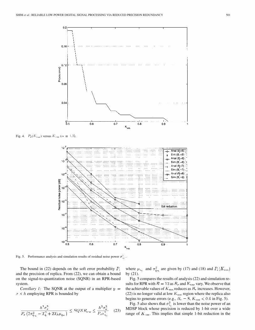
Proof: See Appendix B.Note that Fig. 4 shows a plot of error probability function in
(21) for a 8 8 Baugh-Wooley multiplier whose delay distribu-tion was shown in Fig. 2. We observe that the error probabilitydoes not increase significantly until approaches 0.7. In ad-dition, only about 5% of inputs result in output errors even at
.We now seek an upper and a lower bound on the noise power
in the RPR system by combining and ,Theorem 1: For a given VOSF , the residual noise
power at the output of a multiplier in an RPR-based systemis bounded by
(22)
Proof: See Appendix C.
SHIM et al.: RELIABLE LOW-POWER DIGITAL SIGNAL PROCESSING VIA REDUCED PRECISION REDUNDANCY 501
Fig. 4. P (K ) versus K (� = 1:2).
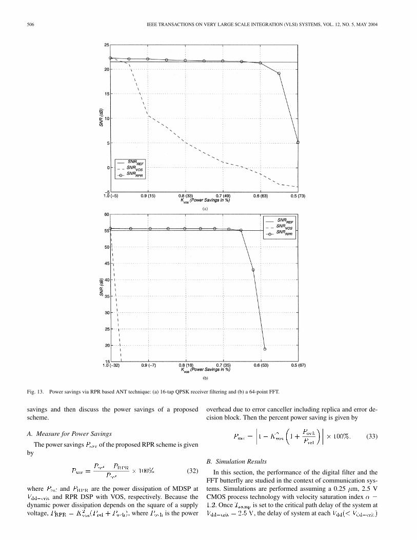
Fig. 5. Performance analysis and simulation results of residual noise power � .
The bound in (22) depends on the soft error probabilityand the precision of replica. From (22), we can obtain a boundon the signal-to-quantization noise (SQNR) in an RPR-basedsystem.
Corollary 1: The SQNR at the output of a multiplieremploying RPR is bounded by
(23)
where and are given by (17) and (18) andby (21).
Fig. 5 compares the results of analysis (22) and simulation re-sults for RPR with as and vary. We observe thatthe achievable values of reduces as increases. However,(22) is no longer valid at low region where the replica alsobegins to generate errors (e.g., , in Fig. 5).
Fig. 5 also shows that is lower than the noise power of anMDSP block whose precision is reduced by 1-bit over a widerange of . This implies that simple 1-bit reduction in the
502 IEEE TRANSACTIONS ON VERY LARGE SCALE INTEGRATION (VLSI) SYSTEMS, VOL. 12, NO. 5, MAY 2004
TABLE IALGORITHM TO DETERMINE THE OPTIMUM REPLICA PRECISION B
MDSP precision at will give a lower SNR than RPRindicating that RPR provides nontrivial benefits.
E. Optimum Precision Selection
The dynamic power dissipation of an original MDSP systemat is given by
(24)
where is the effective capacitance of the MDSP and isthe system clock frequency. The power dissipation of an RPR-based system is given by
(25)
where is the effective switching capacitance of the errorcontrol block. In order to guarantee power savings, i.e.,
, we can show from (24) and (25) that
(26)
As mentioned, noise power in the RPR scheme dependson soft error probability and the replica precision . Notethat will be reduced when is high at the expense ofpower. Likewise, trades off performance and power as afunction of [see (21)]. Therefore, our goal is to determinevalues for and that results in minimum power dissi-pation while satisfying the SNR requirements. The problem isexpressed as follows:
(27)
subject to
(28)
(29)
The solution of problem stated in (27)–(29) can be found usinga two dimensional search method which can be implementedeasily. The key idea is to search for a boundary point of two di-mensional regions consisting of and axis which satis-fies noise and power constraints. Specifically, for a given ,
Fig. 6. Illustration of optimum replica precision search.
we increase (vertical axis in Fig. 6) until it satisfies (28)and then repeat this step for the next . Notice that we donot need to increase beyond the boundary point since thepower consumption only increases. This algorithm is describedin Table I.
The feasible region and power consumption for 12 12 bitmultiplier-and-accumulator (MAC), found by the proposed al-gorithm, is shown in Fig. 7(a), where we used a 32 tap low-passfilter with cutoff frequency and the constraint of noisepower is assumed. We also assumed the lumpedcapacitance of MAC to be proportional to [22]. Itcan be seen from Fig. 7(b) that at each , the point of max-imum power savings occurs at the boundary. By following thesearch procedure described above, we obtained ,and the optimum power savings of 63.25% at a replica precisionof . Note that if is decreased beyond this point, softerror probability will increase abruptly and noise power con-straints would not be satisfied.
III. RPR DIGITAL SIGNAL PROCESSOR
In this section, we describe DSP architectures for RPR basedsystems. Two of the most common DSP applications used incommunication systems are digital filtering and FFT. Thus, wedevelop the RPR architectures for the MAC in digital filters andmultipliers in FFT processors.
SHIM et al.: RELIABLE LOW-POWER DIGITAL SIGNAL PROCESSING VIA REDUCED PRECISION REDUNDANCY 503
Fig. 7. Precision optimization for the replica in a 12� 12 bit MAC MDSP system. (a) Feasible region. (b) Power savings.
A. RPR for Digital Filtering
Fig. 8(a) shows the proposed folded RPR FIR architecture.Along with the main MAC, a replica MAC is employed for gen-erating estimates of main MAC. The operands to the replicaMAC are the same as the main MAC but have a smaller pre-cision, which makes it immune to VOS errors. After executingan -tap multiply-accumulate operation, the results of the mainMAC and replica MAC are compared for error detection. If anerror is detected then the result of the replica MAC is chosen,otherwise, the main MAC output is selected as the final output.
Fig. 8(b) shows an unfolded RPR digital filter. The unfoldedRPR filtering has a one cycle latency. However, it does notsuffers any loss in throughput. The overhead of the proposedscheme includes the replica filter and the decision block (sub-tractor and comparator). Employing the fact that soft errors aremostly of large magnitude, the complexity of the error con-trol block can be reduced significantly, as will be discussed inSection III-C.
B. RPR for FFT
Here, we consider a radix-2 decimation-in-time (DIT) basedFFT processor. The processor’s datapath computes one complexradix-2 DIT butterfly per cycle [23]. As shown in Fig. 9(a), theDIT butterfly calculates two outputs, and
, from two inputs and , and a twiddlefactor . It is assumed that appropriate pipelining is employedto route data between the memory and the functional units inorder to maximize throughput. Apart from the main memory,multipliers are the largest functional units in a VLSI implemen-tation of such a processor [24].
In this paper, we consider a 64-point FFT processor with16-bit precision operating on 10-bit fixed-point complexinputs, which are typical parameters for an FFT in a wirelesslocal area network (WLAN) orthogonal frequency divisionmultiplexing (OFDM) modem [25]. Four multipliers alongwith two adders multiply and and four additional addersgenerate the stage output and . Since the fixed-point data
504 IEEE TRANSACTIONS ON VERY LARGE SCALE INTEGRATION (VLSI) SYSTEMS, VOL. 12, NO. 5, MAY 2004
Fig. 8. Proposed RPR based digital filtering: (a) DSP architecture and (b) its application in an FIR filter.
Fig. 9. Proposed RPR based MAC architecture for FFT: (a) butterfly in DIT FFT, and (b) architecture of multiplier employing RPR.
SHIM et al.: RELIABLE LOW-POWER DIGITAL SIGNAL PROCESSING VIA REDUCED PRECISION REDUNDANCY 505
Fig. 10. Path-delay distribution of an 8� 8 Baugh-Wooley multiplier.
format requires the eventual truncation of the butterfly outputswhen writing the outputs back to memory, computation ofall the multiplier output bits is unnecessary [23]. Therefore,the outputs of the multipliers are truncated by bits. Themultiplier structure of RPR FFT is shown in Fig. 9(b), where a
bit reduced precision multiplier is employed.The multiplier used in FFT processor is more amenable to
VOS than a general purpose array multiplier due to the factthat the real and imaginary parts of the twiddle factor takeonly distinct values in an -point FFT. For example,in a 16-point FFT, the twiddle factor components take only
distinct values among all the possiblevalues. Fig. 10 compares the path delay histograms of thegeneral purpose multiplier and the FFT multiplier in whichone of the operands takes only the 9 possible twiddle factorvalues. We can easily observe the significant reduction in thepercentage of longer paths. In particular, only 8% of the inputcombinations excite paths with delays longer than 75% of thecritical path delay.
C. Error Control BlockThe error control block described in Sections III-A and B re-
quires a subtractor and a comparator followed by a 2-to-1 mul-tiplexer. As discussed in Section II-B, the maximum differencebetween the replica output and MDSP output at is usedas the decision threshold in the comparator.
The input to the RPR MAC (or multiplier) suffers maximumquantization noise when all the truncated bits in the operandare 1. We denote the number of truncated bits as
and use integer representation for notational convenience.Since the largest number in magnitude of bits 2’s complementrepresentation is , the maximum difference occurs whenboth input operands are . In this case, the decisionthreshold is
(30)
Fig. 11. Decision block structure.
Fig. 12. Simulation setup for RPR receive filter in QPSK.
Typically, for large and ,. Thus, becomes approximately
(31)
By choosing the threshold in (31), the comparator can be re-alized with the simple circuit consisting of AND, NAND, andOR shown in Fig. 11. Notice that the outputs of NAND and ORgate need to be logic 1 to enable the ctrl signal, which corre-sponds to the condition . This is much sim-pler than a full-blown implementation requiring -bit fulladder. Even in the case where one operand is fixed, a similarstructure can be employed by recognizing the fact that perfor-mance is insensitive to small changes in the threshold.
IV. SIMULATION RESULTS AND DISCUSSION
In this section, we discuss the performance of the proposedRPR ANT technique. First, we define the measure for power
506 IEEE TRANSACTIONS ON VERY LARGE SCALE INTEGRATION (VLSI) SYSTEMS, VOL. 12, NO. 5, MAY 2004
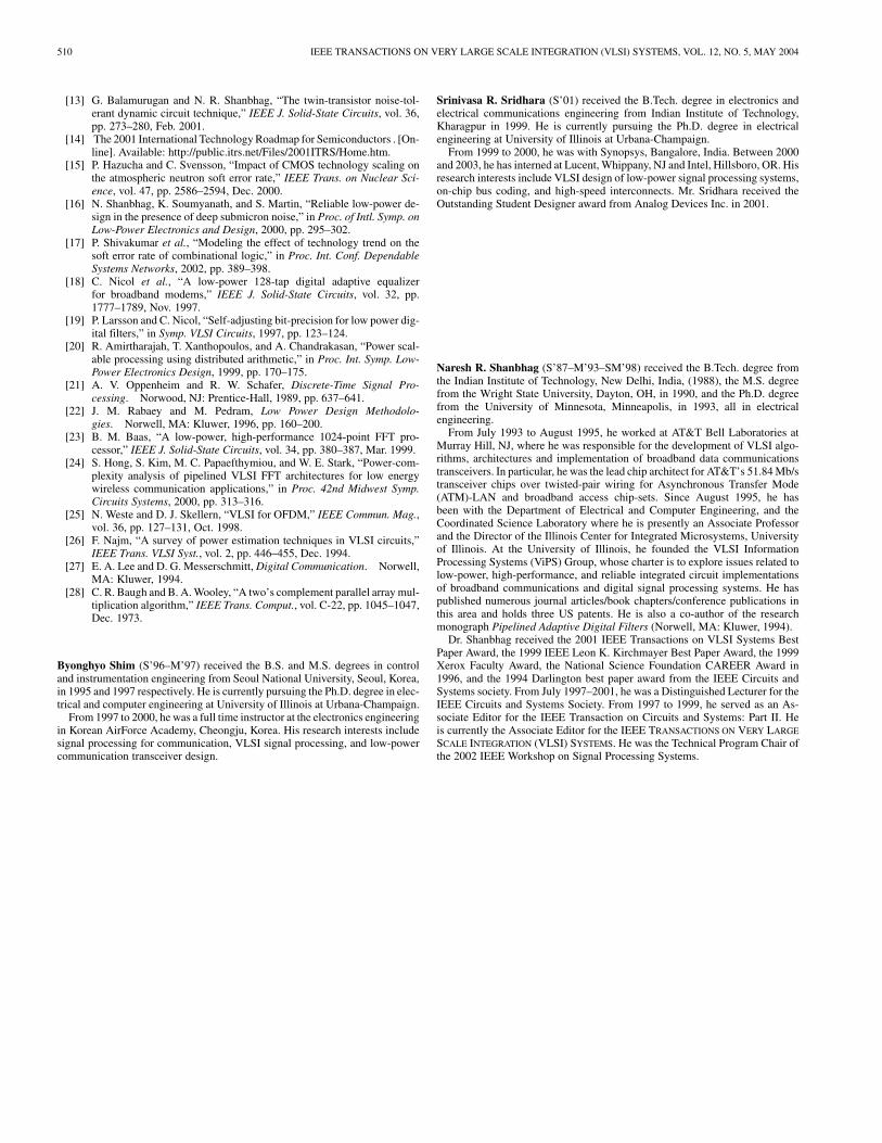
Fig. 13. Power savings via RPR based ANT technique: (a) 16-tap QPSK receiver filtering and (b) a 64-point FFT.
savings and then discuss the power savings of a proposedscheme.
A. Measure for Power Savings
The power savings of the proposed RPR scheme is givenby
(32)
where and are the power dissipation of MDSP atand RPR DSP with VOS, respectively. Because the
dynamic power dissipation depends on the square of a supplyvoltage, , where is the power
overhead due to error canceller including replica and error de-cision block. Then the percent power saving is given by
(33)
B. Simulation Results
In this section, the performance of the digital filter and theFFT butterfly are studied in the context of communication sys-tems. Simulations are performed assuming a 0.25 m, 2.5 VCMOS process technology with velocity saturation index
. Once is set to the critical path delay of the system at, the delay of system at each
SHIM et al.: RELIABLE LOW-POWER DIGITAL SIGNAL PROCESSING VIA REDUCED PRECISION REDUNDANCY 507
Fig. 14. Power savings for various FFT sizes.
is obtained by scaling using (19). At each , the gate-levelpower simulator MED [26] is employed to estimate the energysavings obtained via voltage reduction as proposed.
In the simulations for digital filter, receive filtering of a QPSKcommunication system in the presence of AWGN noise is con-sidered. To achieve bit error rate of , decoder slicer inputSNR should be 21.5 dB including a 6 dB margin [27]. Con-ventional filters (optimized at ) have been designed tomeet this performance specification, where 16 taps withbit MAC satisfies the requirements with minimal complexity.The replica MAC precision bit and, in both cases, aBaugh-Wooley signed multiplier is employed [28]. The plot of
versus SNR for receiver equalization employing the pro-posed RPR scheme is shown in Fig. 13(a). While the conven-tional filter suffers sharp SNR drop when is reduced, theproposed RPR technique maintains desired performance near
. In this case, achievable energy savings over a con-ventional MAC that operates at is 60%. Note that theerror rate at this value of is 0.09/sample. Beyond this point,VOS affects the replica MAC and therefore the assumption inSection II-B is violated. As a result, reliable error control is nolonger possible.
For the FFT butterfly simulations, we consider an FFT pro-cessor that has typical WLAN OFDM parameters [25] with FFTlength , FFT precision bits and input preci-sion of 10 bits. The inputs of replica multipliers are truncatedby and the internal truncation is set to 12 bits for thereference multiplier and 9 bits for the replica. Fig. 13(b) plotsSNR versus and the corresponding power savings. The
when equals 55 dB. We can observethat is satisfied until (ap-proximately 44% power savings) while falls off rapidlyeven when decreases slightly. The error rate at this value of
is 0.06/sample. Note that about 27% power savings can be
achieved by directly reducing the FFT precision by 1-bit withoutVOS. This, however, results in an SNR loss of 3 dB which failsto meet the SNR requirements.
The achievable power savings for the proposed FFT schemedepends on the length and precision of the FFT due to varia-tion in the path delay distribution. Fig. 14 shows the variationof power savings with FFT precision of and FFT length
. When the precision is fixed, power savings decrease with in-crease in FFT length since the frequency of longer paths that failat a given increases. We also observe that power savingsincrease with the FFT precision.
Finally, in order to compare the area overhead of RPR systemover the conventional MDSP, we synthesized layouts for bothsystems in 0.25 m process technology. We designed the receivefilter for QPSK system described earlier using VHDL and syn-thesized the layouts via Synopsys Design Analyzer and CadenceSilicon Ensemble. We also estimated the power consumption viaNanosim. Fig. 15 shows the layouts for MDSP and the proposedRPR system, respectively. We define the area overhead of RPRover the MDSP as
(34)
Substituting m and min (34), we obtain the area overhead . In addition, thepower consumption of MDSP layout at is229 @ 100 MHz and that of RPR at 0.65 is 96@ 100 MHz resulting in power savings of 58.1%. This exampleclearly demonstrates the power savings achievable throughRPR. These power savings can be improved significantly byemploying separate supplies for the replica and the MDSPblocks and sizing the replica transistors differently from thosein the MDSP block.
508 IEEE TRANSACTIONS ON VERY LARGE SCALE INTEGRATION (VLSI) SYSTEMS, VOL. 12, NO. 5, MAY 2004
(a) (b)
Fig. 15. Synthesized layouts of: (a) MDSP and (b) RPR.
V. CONCLUSIONS
In this paper, we have proposed a novel algorithmic noise-tol-erance technique referred to as reduced precision redundancy(RPR) to combat errors in hardware. Combining ANT and VOSresults in soft digial signal processing systems that consumemuch less power than systems operating error-free at criticalsupply voltages. The RPR scheme was shown to be very effec-tive in mitigating system-level errors via analysis, and simula-tions on circuit layouts in 0.25- m CMOS for a QPSK receivefilter and an FFT block.
Soft digital signal processing systems can reduce leakagepower and provide robustness to errors caused by leakagecurrents. This topic requires future study. Noise sources suchas cosmic rays and alpha particles can impact the error-controlblocks as well. Future research needs to be directed toward theproblem of efficient error-control in the presence of errors inthe error-correction blocks. ANT is an elegant approach fortrading-off reliability and energy-efficiency in deep submicronsystems.
APPENDIX APROOF OF LEMMA 2
The quantization noise in a multiplication is defined as. The mean is
(A-1)
Since is deterministic, we get
(A-2)
where has been computed in Lemma 1. Substituting from(13) and using as is uniformly distributed in ,we get
(A-3)
The power is
(A-4)
Using , we get
(A-5)
APPENDIX BPROOF OF LEMMA 3
Consider a path with logic gates. When the supply voltageis reduced from to , the delay for a single gate[see (19)] increases to
(B-1)
Clearly the original path delay becomes. Therefore, as shown in Fig. 16, shaded re-
gion in an original delay distribution becomes VOS error region
SHIM et al.: RELIABLE LOW-POWER DIGITAL SIGNAL PROCESSING VIA REDUCED PRECISION REDUNDANCY 509
Fig. 16. VOS error region for the path delay distribution variation.
and the error probability is obtained by integrating this region,i.e., . By using (19) and (B-1), one can show
that the point which starts to generate an error when VOSis applied is
(B-2)
Thus, VOS error probability is now given by
Note that .
APPENDIX CPROOF OF THEOREM 1
In this proof, we drop the time index for notational conve-nience. Recall that the quantization noise power employingRPR is
(C-1)
If is chosen according to (5), no false alarm event can occurduring error detection and hence three possible scenarios exist:(i) no error (C-2), (ii) undetected error (C-3), and (iii) detectederror (C-4).
(C-2)
(C-3)
(C-4)
Thus, (C-1) can be rewritten as
(C-5)
Note that there is no information loss in scenario (i) and fromscenarios (ii) and (iii)
(C-6)
Thus, (C-5) becomes
(C-7)
In most cases, the magnitude of VOS error is large and hencedetected, i.e., . Thus
(C-8)
where .By using the auxiliary variable , we have
(C-9)
In addition, as from scenario (ii) (see (C-3)),(C-9) can be simplified to
(C-10)
By substituting (C-10) into (C-7), we obtain
(C-11)
(C-12)
REFERENCES
[1] B. Davari, R. H. Dennard, and G. G. Shahidi, “CMOS scaling for high-performance and low power—The next ten years,” Proc. IEEE, vol. 83,pp. 595–606, Apr. 1995.
[2] A. P. Chandrakasan and R. W. Brodersen, “Minimizing power consump-tion in digital CMOS circuits,” Proc. IEEE, vol. 83, pp. 498–523, Apr.1995.
[3] R. Gonzalez, B. Gordon, and M. Horowitz, “Supply and thresholdvoltage scaling for low-power CMOS,” IEEE J. Solid-State Circuits,vol. 32, pp. 1210–1216, Aug. 1997.
[4] J. M. Rabaey, Digital Integrated Circuits: A Design Perspec-tive. Englewood Cliffs, NJ: Prentice-Hall, 1996.
[5] K. L. Shepard and V. Narayanan, “Noise in deep submicron digital de-sign,” in Proc. Int. Conf. CAD, Nov. 1996, pp. 524–531.
[6] P. Larsson and C. Svensson, “Noise in digital dynamic CMOS circuits,”IEEE J. Solid-State Circuits, vol. 29, pp. 655–662, Jun. 1994.
[7] G. E. Moore, “Cramming more components onto integrated circuits,”Proc. IEEE, vol. 86, pp. 82–85, Jan. 1998.
[8] N. R. Shanbhag, “A mathematical basis for power-reduction in digitalVLSI systems,” IEEE Trans. CAS Part II, vol. 44, no. 11, pp. 935–951,Nov. 1997.
[9] R. Hedge and N. R. Shanbhag, “Energy-efficient signal processing viaalgorithmic noise-tolerance,” in Proc. Int. Symp. Low-Power Electronicsand Design, Aug. 1999, pp. 30–35.
[10] , “Soft digital signal processing,” IEEE Trans. on VLSI, vol. 9, no.6, pp. 813–823, Dec. 2001.
[11] , “A low-power digital filter IC via soft DSP,” in Proc. of CICC,May 2001, pp. 309–312.
[12] L. Wang and N. R. Shanbhag, “Low-power filtering via adaptive error-cancellation,” IEEE Trans. Signal Processing, vol. 51, pp. 575–583, Feb.2003.
510 IEEE TRANSACTIONS ON VERY LARGE SCALE INTEGRATION (VLSI) SYSTEMS, VOL. 12, NO. 5, MAY 2004
[13] G. Balamurugan and N. R. Shanbhag, “The twin-transistor noise-tol-erant dynamic circuit technique,” IEEE J. Solid-State Circuits, vol. 36,pp. 273–280, Feb. 2001.
[14] The 2001 International Technology Roadmap for Semiconductors . [On-line]. Available: http://public.itrs.net/Files/2001ITRS/Home.htm.
[15] P. Hazucha and C. Svensson, “Impact of CMOS technology scaling onthe atmospheric neutron soft error rate,” IEEE Trans. on Nuclear Sci-ence, vol. 47, pp. 2586–2594, Dec. 2000.
[16] N. Shanbhag, K. Soumyanath, and S. Martin, “Reliable low-power de-sign in the presence of deep submicron noise,” in Proc. of Intl. Symp. onLow-Power Electronics and Design, 2000, pp. 295–302.
[17] P. Shivakumar et al., “Modeling the effect of technology trend on thesoft error rate of combinational logic,” in Proc. Int. Conf. DependableSystems Networks, 2002, pp. 389–398.
[18] C. Nicol et al., “A low-power 128-tap digital adaptive equalizerfor broadband modems,” IEEE J. Solid-State Circuits, vol. 32, pp.1777–1789, Nov. 1997.
[19] P. Larsson and C. Nicol, “Self-adjusting bit-precision for low power dig-ital filters,” in Symp. VLSI Circuits, 1997, pp. 123–124.
[20] R. Amirtharajah, T. Xanthopoulos, and A. Chandrakasan, “Power scal-able processing using distributed arithmetic,” in Proc. Int. Symp. Low-Power Electronics Design, 1999, pp. 170–175.
[21] A. V. Oppenheim and R. W. Schafer, Discrete-Time Signal Pro-cessing. Norwood, NJ: Prentice-Hall, 1989, pp. 637–641.
[22] J. M. Rabaey and M. Pedram, Low Power Design Methodolo-gies. Norwell, MA: Kluwer, 1996, pp. 160–200.
[23] B. M. Baas, “A low-power, high-performance 1024-point FFT pro-cessor,” IEEE J. Solid-State Circuits, vol. 34, pp. 380–387, Mar. 1999.
[24] S. Hong, S. Kim, M. C. Papaefthymiou, and W. E. Stark, “Power-com-plexity analysis of pipelined VLSI FFT architectures for low energywireless communication applications,” in Proc. 42nd Midwest Symp.Circuits Systems, 2000, pp. 313–316.
[25] N. Weste and D. J. Skellern, “VLSI for OFDM,” IEEE Commun. Mag.,vol. 36, pp. 127–131, Oct. 1998.
[26] F. Najm, “A survey of power estimation techniques in VLSI circuits,”IEEE Trans. VLSI Syst., vol. 2, pp. 446–455, Dec. 1994.
[27] E. A. Lee and D. G. Messerschmitt, Digital Communication. Norwell,MA: Kluwer, 1994.
[28] C. R. Baugh and B. A. Wooley, “A two’s complement parallel array mul-tiplication algorithm,” IEEE Trans. Comput., vol. C-22, pp. 1045–1047,Dec. 1973.
Byonghyo Shim (S’96–M’97) received the B.S. and M.S. degrees in controland instrumentation engineering from Seoul National University, Seoul, Korea,in 1995 and 1997 respectively. He is currently pursuing the Ph.D. degree in elec-trical and computer engineering at University of Illinois at Urbana-Champaign.
From 1997 to 2000, he was a full time instructor at the electronics engineeringin Korean AirForce Academy, Cheongju, Korea. His research interests includesignal processing for communication, VLSI signal processing, and low-powercommunication transceiver design.
Srinivasa R. Sridhara (S’01) received the B.Tech. degree in electronics andelectrical communications engineering from Indian Institute of Technology,Kharagpur in 1999. He is currently pursuing the Ph.D. degree in electricalengineering at University of Illinois at Urbana-Champaign.
From 1999 to 2000, he was with Synopsys, Bangalore, India. Between 2000and 2003, he has interned at Lucent, Whippany, NJ and Intel, Hillsboro, OR. Hisresearch interests include VLSI design of low-power signal processing systems,on-chip bus coding, and high-speed interconnects. Mr. Sridhara received theOutstanding Student Designer award from Analog Devices Inc. in 2001.
Naresh R. Shanbhag (S’87–M’93–SM’98) received the B.Tech. degree fromthe Indian Institute of Technology, New Delhi, India, (1988), the M.S. degreefrom the Wright State University, Dayton, OH, in 1990, and the Ph.D. degreefrom the University of Minnesota, Minneapolis, in 1993, all in electricalengineering.
From July 1993 to August 1995, he worked at AT&T Bell Laboratories atMurray Hill, NJ, where he was responsible for the development of VLSI algo-rithms, architectures and implementation of broadband data communicationstransceivers. In particular, he was the lead chip architect for AT&T’s 51.84 Mb/stransceiver chips over twisted-pair wiring for Asynchronous Transfer Mode(ATM)-LAN and broadband access chip-sets. Since August 1995, he hasbeen with the Department of Electrical and Computer Engineering, and theCoordinated Science Laboratory where he is presently an Associate Professorand the Director of the Illinois Center for Integrated Microsystems, Universityof Illinois. At the University of Illinois, he founded the VLSI InformationProcessing Systems (ViPS) Group, whose charter is to explore issues related tolow-power, high-performance, and reliable integrated circuit implementationsof broadband communications and digital signal processing systems. He haspublished numerous journal articles/book chapters/conference publications inthis area and holds three US patents. He is also a co-author of the researchmonograph Pipelined Adaptive Digital Filters (Norwell, MA: Kluwer, 1994).
Dr. Shanbhag received the 2001 IEEE Transactions on VLSI Systems BestPaper Award, the 1999 IEEE Leon K. Kirchmayer Best Paper Award, the 1999Xerox Faculty Award, the National Science Foundation CAREER Award in1996, and the 1994 Darlington best paper award from the IEEE Circuits andSystems society. From July 1997–2001, he was a Distinguished Lecturer for theIEEE Circuits and Systems Society. From 1997 to 1999, he served as an As-sociate Editor for the IEEE Transaction on Circuits and Systems: Part II. Heis currently the Associate Editor for the IEEE TRANSACTIONS ON VERY LARGE
SCALE INTEGRATION (VLSI) SYSTEMS. He was the Technical Program Chair ofthe 2002 IEEE Workshop on Signal Processing Systems.