253
ELECTRONIC DEVICES AND CIRCUITS (ECE) II B.Tech III semester (IARE - R18) (2019 - 2020) Institute of Aeronautical Engineering

ELECTRONIC DEVICES AND CIRCUITS (ECE)II B.Tech III semester
(IARE - R18)(2019 - 2020)
Institute of Aeronautical Engineering

SYLLABUS
Module-1:DIODE APPLICATIONS
Module-2:BIPOLAR JUNCTION TRANSISTOR (BJT)
Module-3:TRANSISTOR BIASING AND STABILIZATION
Module-4: JUNCTION FIELD EFFECT TRANSISTOR
Module-5:FET AMPLIFIERS
UNIT-I
DIODE AND APPLICATIONS

4
Based on the electrical properties of the materials like conductivity, materials are divided into three types.
i) Conductorsii) Semiconductorsiii) Insulators
Fig.1: Energy band diagrams for insulator, semiconductor and conductor
MATERIALS

CONDUCTORS
• A conductor is a material which supports a generous flow
of charge when a voltage is applied across its terminals.
i.e. it has very high conductivity.
• Ex: Copper, Aluminum, Silver, and Gold. The resistivity of a
conductor is in the order of 10-4 and 10-6 Ω-cm.
5

INSULATORS
6
• An insulator is a material that offers a very low level ofconductivity when voltage is applied.
• Ex: Paper, Mica, glass, quartz.
• Typical resistivity level of an insulator is of the order of 1010
to 1012 Ω-cm.

• A semiconductor is a material that has its conductivity lies
between the insulator and conductor.
• The resistivity level is in the range of 10 and 104 Ω-cm.
• Ex: Si & Ge
7
SEMICONDUCTORS

TYPES OF SEMICONDUCTORS
i) Intrinsic Semiconductor:
• A pure form of semiconductor is called as intrinsic
semiconductor.
• Conduction in intrinsic sc is either due to thermal excitation
or crystal defects.
• Ex: Si and Ge
8

9
ii) Extrinsic Semiconductor:
• The current conduction capability of intrinsic semiconductor can be increased significantly by adding a small amount of impurity to the intrinsic semiconductor.
• By adding impurities it becomes impure or extrinsic semiconductor.
• The process of adding impurities to the intrinsic semiconductor iscalled as doping.
TYPES OF SEMICONDUCTORS

10
A PN junction is a device formed by joining p-type with n-type
semiconductors and separated by a thin junction is called PN
Junction diode or junction diode.
WHAT DO YOU MEAN BY DIODE?

THEORY OF P-N JUNCTION
When a p-type semiconductor material is suitably joined to n-type semiconductor the contact surface is called a p-n junction.
P N
11
+ +
Depletion region

12
THEORY OF PN JUNCTION DIODE
• Suppose the two pieces are suitably treated to form PN
junction, then there is a tendency for the free electrons
from n-type to diffuse over to the p-side and holes from p-
type to the n-side . This process is called diffusion.
• The holes from the p-side diffuse to the n-side and the
electrons from the n-side diffuse to the p-side. This gives
rise to a diffusion current across the junction.

13
THEORY OF PN JUNCTION DIODE
As the free electrons move across the junction from n-type to
p-type, +ve donor ions are uncovered. Hence a +ve charge is
built on the n-side of the junction.
At the same time, the free electrons cross the junction and
uncover the –ve acceptor ions by filling in the holes.
Therefore a net –ve charge is established on p-side of the
junction.

14
THEORY OF PN JUNCTION DIODE
• When a sufficient number of donor and acceptor ions is
uncovered further diffusion is prevented.
• Thus a barrier is set up against further movement of charge
carriers. This is called potential barrier or junction barrier Vo.
The potential barrier is of the order of 0.1 to 0.3V.
• Note: outside this barrier on each side of the junction, the
material is still neutral. Only inside the barrier, there is a +ve
charge on n-side and –ve charge on p-side. This region is called
depletion layer.

15
THEORY OF PN JUNCTION DIODE
• The depletion layer contains no free and mobile charge carriersbut only fixed and immobile ions.
• Its width depends upon the doping level..
• Heavily doped……..thin depletion layer
• lightly doped……..thick depletion layer

16
THEORY OF PN JUNCTION DIODE
PN junction can basically work in two modes, (A battery isconnected to the diode ).
Forward bias mode : positive terminal connected to p-region and negative terminal connected to n region.
Reverse bias mode: negative terminal connected to p-region and positive terminal connected to n region

17
PN JUNCTION –FORWARD BIAS
• It forces the majority charge carriers to move across thejunction ….decreasing the width of the depletion layer.

When a diode is connected in a FB condition, a negative voltageis applied to the N-type material and a positive voltage isapplied to the P-type material.
If this external voltage becomes greater than the value of thepotential barrier, i.e. 0.7V for Si and 0.3V for Ge, the potentialbarriers opposition will be overcome and current will start.
The application of a FB voltage on the junction diode results inthe depletion layer becoming very thin which represents a lowimpedance path through the junction thereby allowing highcurrents to flow.
PN junction –Forward Bias
18

The free electrons and free holes are attracted towards thebattery, hence depletion layer width increases.
PN JUNCTION –REVERSE BIAS
19

PN JUNCTION –REVERSE BIAS
20
• When a diode is connected in a Reverse bias condition, apositive voltage is applied to the N-type material and anegative voltage is applied to the P-type material.
• The positive voltage applied to the N-type material attractselectrons towards the positive electrode and away from thejunction, while the holes in the P-type end are also attractedaway from the junction towards the negative electrode.
• The net result is that the depletion layer grows wider due to alack of electrons and holes and presents a high impedancepath, almost an insulator. The result is that a high potentialbarrier is created thus preventing current from flowing throughthe semiconductor material.

21
V-I CHARACTERISTICS OF PN JUNCTION DIODE
V-I characteristics of PN junction diode

22
V-I CHARACTERISTICS OF PN JUNCTION DIODE
•When the diode is F.B., the current increasesexponentially with voltage except for a small range closeto the origin.
•When the diode is R.B., the reverse current is constant
and independent of the applied reverse bias.
•Turn-on or cut-in (threshold) voltage Vγ: for a F.B. diode itis the voltage when the current increases appreciablyfrom zero.
•It is roughly equal to the barrier p.d.:
•For Ge, Vγ ~ 0.2 – 0.4 V (at room temp.) For Si, Vγ ~ 0.6 –
0.8 V (at room temp.)

23
STATIC OR DC RESISTANCE
The resistance of a diode at a particular operating point is called the dc or static resistance diode.
The resistance of the diode at the operating point can be found simply by finding the corresponding levels of VD
and ID.
It can be determined using equation
RD =VD/ID
The lower current through a diode the higher the dc resistance level
Fig: Static resistance curve

24
DYNAMIC OR AC RESISTANCE
Static resistance is using dc
input. If the input is sinusoidal
the scenario will be change.
The ac resistance is determinedby a straight line drawn betweenthe two intersections of themaximum and minimum valuesof input voltage.Thus the specific changes incurrent and voltage is obtained.It can be determined usingequation rd = ∆VD/ ∆ID
Fig: Dynamic resistance curve
25
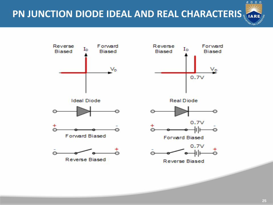
PN JUNCTION DIODE IDEAL AND REAL CHARACTERISTICS

26
DIODE EQUIVALENT CIRCUIT
When a diode is F.B, we can use the approximatemodel for the on state

27
PN DIODE- LOAD LINE ANALYSIS
• The curve shows the diode response (I vs VD) while the straight line shows the behavior of the linear part of the circuit:
I=(VDD-VD)/R.• The point of intersection gives the actual current and voltage.
A load line is a line drawn on the characteristic curve, a graph of the current vs. voltage in a nonlinear device like a diode.

28
JUNCTION CAPACITANCE
In a p-n junction diode, two types of capacitance take place. They are,• Transition capacitance (CT)• Diffusion capacitance (CD)
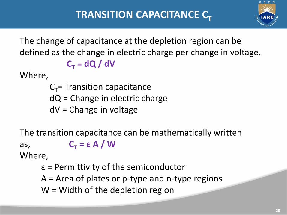
Transition Capacitance CT
The amount of capacitance changed with increase in voltage is called transition capacitance. The transition capacitance is also known as depletion region capacitance, junction capacitance or barrier capacitance.
29
TRANSITION CAPACITANCE CT
The change of capacitance at the depletion region can be defined as the change in electric charge per change in voltage.
CT = dQ / dVWhere,
CT= Transition capacitancedQ = Change in electric chargedV = Change in voltage
The transition capacitance can be mathematically written as, CT = ε A / WWhere,
ε = Permittivity of the semiconductorA = Area of plates or p-type and n-type regionsW = Width of the depletion region

30
DIFFUSION CAPACITANCE (CD)
Diffusion capacitance occurs in a forward biased p-n junction diode. Diffusion capacitance is also sometimes referred as storage capacitance. It is denoted as CD.
The formula for diffusion capacitance isCD = dQ / dV
Where,CD = Diffusion capacitancedQ = Change in number of minority carriers stored
outside the depletion regiondV = Change in voltage applied across diode
31
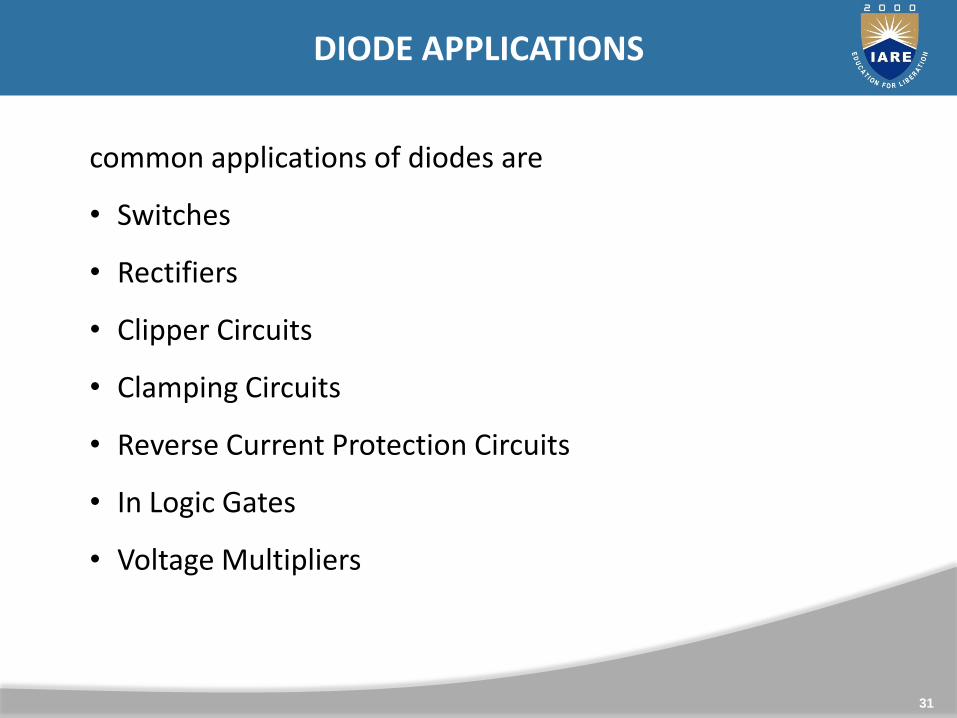
DIODE APPLICATIONS
common applications of diodes are
• Switches
• Rectifiers
• Clipper Circuits
• Clamping Circuits
• Reverse Current Protection Circuits
• In Logic Gates
• Voltage Multipliers

32
PN DIODE SWITCHING TIMES
•The majority carriers in P-type (holes)
= Ppo
•The majority carriers in N-type (electrons)
= Nno
•The minority carriers in P-type (electrons)
= Npo
•The majority carriers in N-type (holes)
= Pno

33
PN DIODE SWITCHING TIMES
Storage time − The time period for which the diode remains in the conduction state even in the reverse biased state, is called as Storage time.Transition time − The time elapsed in returning back to the state of non-conduction, i.e. steady state reverse bias, is called Transition time.Reverse recovery time − The time required for the diode to change from forward bias to reverse bias is called as Reverse recovery time.Forward recovery time − The time required for the diode to change from reverse bias to forward bias is called as Forward recovery time.

34
RECTIFIER
• A circuit that converts ac voltage of main supply into pulsating dc voltage using one or more PN junction diodes is called rectifier.
• Half Wave Rectifier
• Full Wave Rectifier
• Bridge Rectifier
35
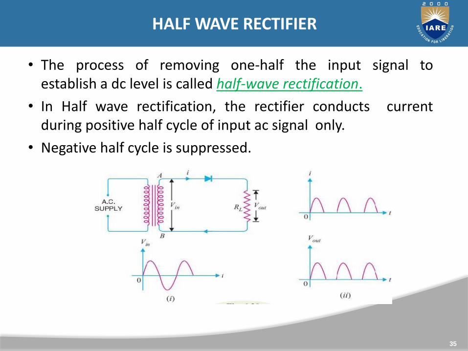
HALF WAVE RECTIFIER
• The process of removing one-half the input signal toestablish a dc level is called half-wave rectification.
• In Half wave rectification, the rectifier conducts currentduring positive half cycle of input ac signal only.
• Negative half cycle is suppressed.
36
HALF WAVE RECTIFIER
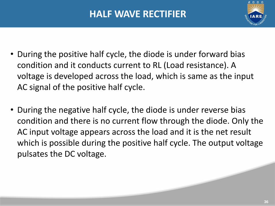
• During the positive half cycle, the diode is under forward bias condition and it conducts current to RL (Load resistance). A voltage is developed across the load, which is same as the input AC signal of the positive half cycle.
• During the negative half cycle, the diode is under reverse bias condition and there is no current flow through the diode. Only the AC input voltage appears across the load and it is the net result which is possible during the positive half cycle. The output voltage pulsates the DC voltage.

37
HALF WAVE RECTIFIER
Average DC load Current (IDC ):

38
HALF WAVE RECTIFIER
Average DC voltage (Edc):

39
HALF WAVE RECTIFIER
RMS Load Current (Irms):
RMS Load Voltage (Erms):
Peak Inverse Voltage (PIV):
PIV = EmDiode must be selected based on the PIV rating andthe circuit specification.

40
HALF WAVE RECTIFIER
DC Power Delivered to the load:

41
HALF WAVE RECTIFIER
AC input power from transformer secondary:

42
HALF WAVE RECTIFIER
Rectifier Efficiency (η):
; η= 40.6 %
Under best conditions (no diode loss) only 40.6% of the ac input
power is converted into dc power.
The rest remains as the ac power in the load

43
HALF WAVE RECTIFIER
Ripple Factor:
This indicates that the ripple content in the output are 1.211 times the dc component.
i.e. 121.1 % of dc component.
(or)

44
HALF WAVE RECTIFIER
Disadvantage of HWR:
• The ripple factor of half wave rectifier is 1.21, which is quite high.
• The output contains lot of ripples• The maximum theoretical efficiency is 40%.• The practical value will be quite less than this.• This indicates that HWR is quite inefficient.
45
FULL-WAVE RECTIFIER
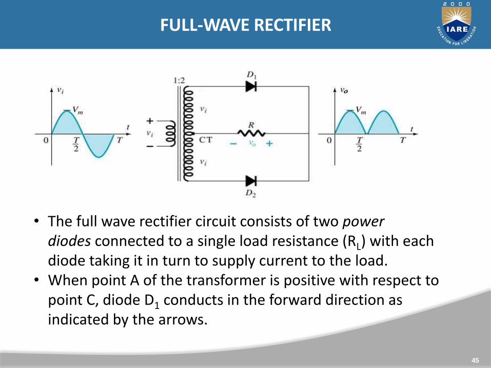
• The full wave rectifier circuit consists of two power diodes connected to a single load resistance (RL) with each diode taking it in turn to supply current to the load.
• When point A of the transformer is positive with respect to point C, diode D1 conducts in the forward direction as indicated by the arrows.

46
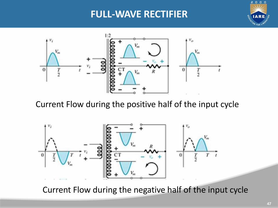
FULL-WAVE RECTIFIER
• When point B is positive (in the negative half of the cycle) with respect to point C, diode D2 conducts in the forward direction and the current flowing through resistor R is in the same direction for both half-cycles.
• As the output voltage across the resistor R is the phasor sum of the two waveforms combined, this type of full wave rectifier circuit is also known as a “bi-phase” circuit.
47
FULL-WAVE RECTIFIER
Current Flow during the positive half of the input cycle
Current Flow during the negative half of the input cycle
48
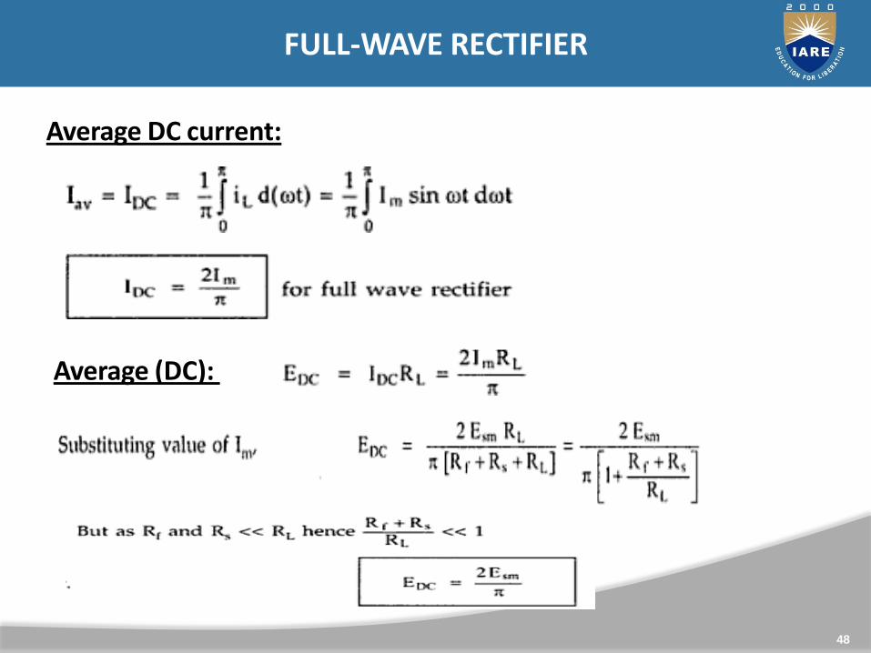
FULL-WAVE RECTIFIER
Average DC current:
Average (DC): Voltage

49
FULL-WAVE RECTIFIER
RMS Load Current (Irms):
RMS Load Voltage:
DC Output Power:

50
FULL-WAVE RECTIFIER
AC input power (Pac):
Rectifier Efficiency (η):
=> =>

51
FULL-WAVE RECTIFIER
Ripple Factor:
This indicates that the ripple contents in the output are 48%of the dc component which is much less than that for thehalf wave rectifier.

52
FULL-WAVE RECTIFIER
Peak Inverse Voltage:
53
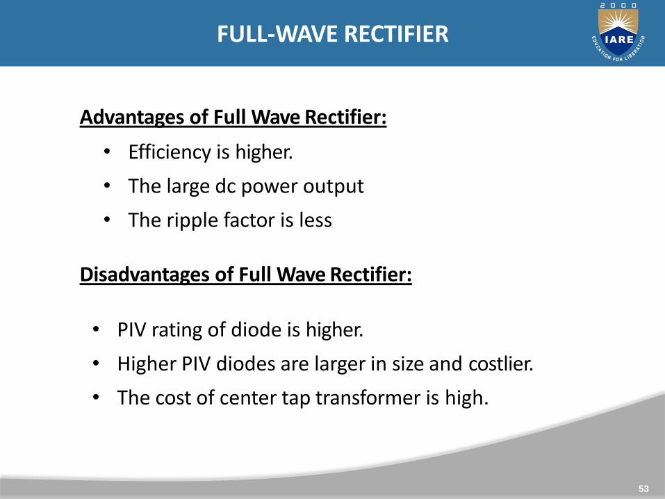
FULL-WAVE RECTIFIER
• Efficiency is higher.
• The large dc power output
• The ripple factor is less
Disadvantages of Full Wave Rectifier:
• PIV rating of diode is higher.
• Higher PIV diodes are larger in size and costlier.
• The cost of center tap transformer is high.
Advantages of Full Wave Rectifier:

54
BRIDGE RECTIFIER
A Bridge rectifier that rectifies mains AC input to DC output. Bridge Rectifiers are widely used in power supplies that provide necessary DC voltage for the electronic components or devices.

55
WORKING OF BRIDGE RECTIFIER
• During the positive half cycle of secondary voltage, the diodes D1 and D2 are forward-biased, but diodes D3 and D4 do no conduct. The current is through D1, R, D2 and secondary winding.
• During the negative half cycle, the diodes D3 and D4 are forward-biased, but diodes D1 and D2 do not conduct. The current is through D3, secondary winding, D4 and R.

56
BRIDGE RECTIFIER WAVEFORMS

57
BRIDGE RECTIFIER PARAMETERS

58
RECTIFIERS WITH CAPACITIVE FILTER
Fig: H/W rectifier with filter Fig: F/W rectifier with filter
• In full wave rectifier circuit using a capacitor filter, the capacitor C is located across the RL load resistor. The working of this rectifier is almost the same as a half wave rectifier.
• Once the i/p AC voltage is applied throughout the positive half cycle, then the D1 diode gets forward biased and permits flow of current while the D2 diode gets reverse biased & blocks the flow of current.
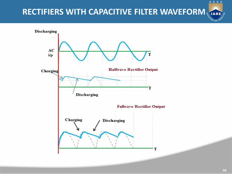
59
RECTIFIERS WITH CAPACITIVE FILTER WAVEFORMS

60
CLIPPERS
Clipper circuits, also called limiter circuits, are used to eliminate portion
of a signal that are above or below a specified level – clip value.
The purpose of the diode is that when it is turn on, it provides the clip
value
Clip value = V’. To find V’, use KVL at L1
The equation is : V’ – VB - V = 0 V’ = VB + V
Then, set the conditions
If Vi > V’, what happens? diode conducts, hence Vo = V’
If Vi < V’, what happens? diode off, open circuit, no current flow, Vo = Vi

61
CLIPPERCIRCUITS
positive clipper:In a positive clipper, the positive half cycles of the input voltage will be removed.
Negative clipper:In a Negative clipper, the negative half cycles of the input voltage will be removed.

62
CLIPPERCIRCUITS
Biased PositiveClipper:
• When the input signal voltage is positive, the diode ‘D’ is reverse-biased. This causes it to act as an open-switch.
When the input signal voltage is negative its also reverse biased but in this case battery voltage is more than the input voltage so its acts like an close switch.
Biased NegativeClipper:

63
TWO LEVEL-CLIPPER
• When a portion of both positive and negative of each half cycle of the input voltage is to be clipped (or removed), combination clipper is employed.

64
CLAMPERS
• A circuit which adds DC value to an AC wave form without changing its waveform.
• In this circuit we use a diode and a capacitor and a resistor for measure voltage in our circuit.

65
WHY CLAMPERUSE?
• Clamper use to increase the wavelength of input wave.
• Like an sound system amplifier.

66
CLAMPERS
In positive clamper diode is forward biased and current flow is maximum.Due to the presence of the capacitor it will double the wavelength on positive side.
In this capacitor negativelycharged and the output isdouble of the input of the negative side.

67
CLAMPING CIRCUIT THEOREM
The clamping circuit theorem states that under steady-state conditions, for any input waveform, the ratio of the area under the output voltage curve in the forward direction to that in the reverse direction is equal to the ratio Rf/R.
In the time interval t1 to t2, D is ON. Hence, during this period, the charge builds up on the capacitor C. If if is the diode current, the charge gained by the capacitor during the interval t1 to t2 is:

68
CLAMPING CIRCUIT THEOREM
However, if = Vf/Rf, where Vf is the diode forward voltage:
During the interval t2 to t3, D is OFF. Hence, the capacitor discharges and the charge lost by C is:
Put ir = Vr/R, where Vr is the diode reverse voltage:

69
CLAMPING CIRCUIT THEOREM
At steady state, the charge gained is equal to the charge lost. In other words, q1 = q2.
Here, Af is the area with D in the ON state and Ar is the area under the output curve with D in the OFF state.
70
COMPARATORS
• An amplitude comparator is a circuit that tells the time instant at which the input amplitude has reached a reference level..
vo = 0 for t < t1vo = V for t ≥ t1
• The distinction between comparator circuits and the clipping circuits is that, in a comparator there is no interest in reproducing any part of the signal waveform, whereas in a clipping circuit, part of the signal waveform is needed to be reproduced without any distortion.

71
COMPARATORS
• Comparators may be non-regenerative or regenerative.• Clipping circuits are non-regenerative comparators. • Schmitt trigger and oscillators are regenerative comparators.

UNIT-IIBIPOLAR JUNCTION TRANSISTOR (BJT)
UNIT-IIBIPOLAR JUNCTION TRANSISTOR (BJT)

Outline
74
Principle of Operation and characteristics
Common Emitter Configuration
Common Base Configuration
Common Collector Configuration
Operating point
DC & AC load lines
Transistor Hybrid parameter model
Determination of h-parameters from transistor characteristics
Conversion of h-parameters
Problems

Principle of Operation and characteristics
75

• The basic of electronic system nowadays is
semiconductor device.
• The famous and commonly use of this device is BJTs
(Bipolar Junction Transistors).
• It can be use as amplifier and logic switches.
• BJT consists of three terminal:
collector : C
base : B
emitter : E
• Two types of BJT : pnp and npn
76
Principle of Operation and characteristics

• 3 layer semiconductor device consisting:
– 2 n- and 1 p-type layers of material npn transistor
– 2 p- and 1 n-type layers of material pnp transistor
• The term bipolar reflects the fact that holes and electrons participate in the injection process into the oppositely polarized material
• A single pn junction has two different types of bias:
– forward bias
– reverse bias
• Thus, a two-pn-junction device has four types of bias.
77
Principle of Operation and characteristics
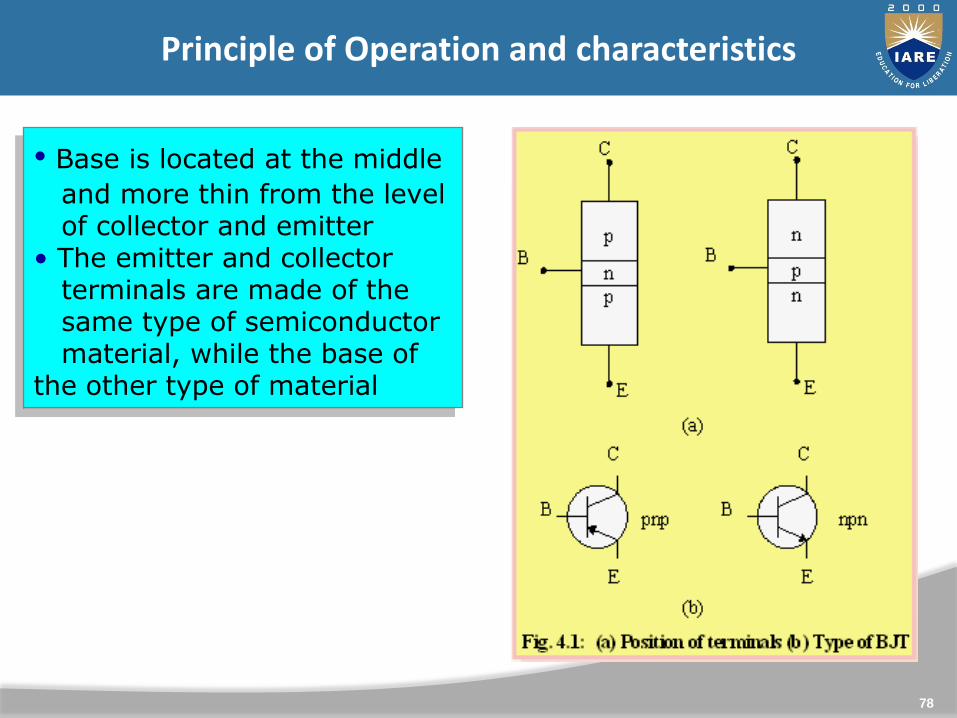
78
Principle of Operation and characteristics
• Base is located at the middle
and more thin from the level of collector and emitter
• The emitter and collector terminals are made of the same type of semiconductor material, while the base of
the other type of material

79
Principle of Operation and characteristics
-The arrow is always drawn
on the emitter
-The arrow always point
toward the n-type
-The arrow indicates the
direction of the emitter
current:
pnp:E B
npn: B E
IC=the collector currentIB= the base currentIE= the emitter current

• The basic operation will be described using the pnp transistor. The operation of the pnp transistor is exactly the same if the roles played by the electron and hole are interchanged.
• One p-n junction of a transistor is reverse-biased, whereas the other is forward-biased.
80
Principle of Operation and characteristics
Forward-biased junction of a pnp transistor
Reverse-biased junction of a pnp transistor
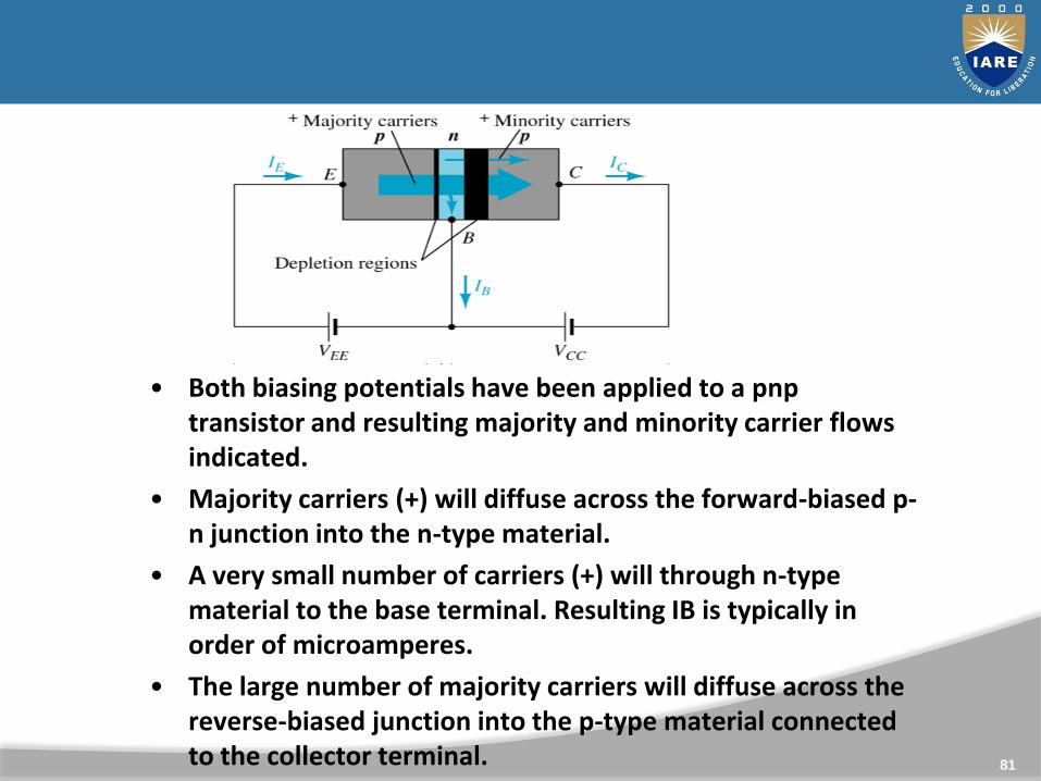
81
• Both biasing potentials have been applied to a pnptransistor and resulting majority and minority carrier flows indicated.
• Majority carriers (+) will diffuse across the forward-biased p-n junction into the n-type material.
• A very small number of carriers (+) will through n-type material to the base terminal. Resulting IB is typically in order of microamperes.
• The large number of majority carriers will diffuse across the reverse-biased junction into the p-type material connected to the collector terminal.

82
•Majority carriers can cross the reverse-biased junction because the injected majority carriers will appear as minority carriers in the n-type material.•Applying KCL to the transistor :
• IE = IC + IB
•The comprises of two components – the majority and minority carriers
• IC = ICmajority + ICOminority
•ICO – IC current with emitter terminal open and is called leakage current.

Common Emitter Configuration
83

• It is called common-emitter configuration since :
- emitter is common or reference to both input and output terminals.
- emitter is usually the terminal closest to or at ground
potential.
• Almost amplifier design is using connection of CE due to the high gain for
current and voltage.
• Two set of characteristics are necessary to describe the behavior for CE
;input (base terminal) and output (collector terminal) parameters
84
Common Emitter Configuration

85
Common Emitter Configuration

86
Common Emitter Configuration
Input characteristics for acommon-emitter NPN transistor
• IB is microamperes compared to miliamperes of IC.
• IB will flow when VBE > 0.7V
for silicon and 0.3V for germanium
• Before this value IB is very small and no IB.
• Base-emitter junction is forward bias
• Increasing VCE will reduce IB
for different values.

87
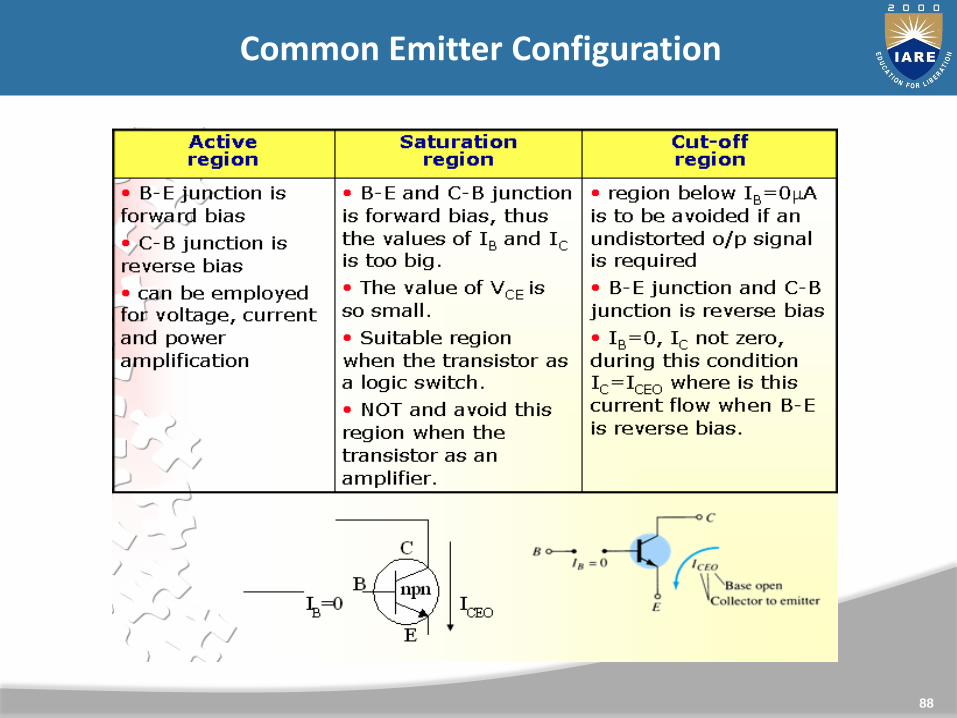
Common Emitter Configuration
Output characteristics for acommon-emitter npn transistor
• For small VCE (VCE < VCESAT, IC increase linearly with increasing of VCE
• VCE > VCESAT IC not totally depends on VCE constant IC
• IB(uA) is very small compare to IC
(mA). Small increase in IB cause big increase in IC
• IB=0 A ICEO occur.
• Noticing the value when IC=0A. There is still some value of current flows.
88
Common Emitter Configuration

89
Common Emitter Configuration
Transistor parameters
Dynamic input resistance (ri)
Dynamic input resistance is defined as the ratio of change in input voltageor base voltage (VBE) to the corresponding change in input current or basecurrent (IB), with the output voltage or collector voltage (VCE) kept atconstant. In CE configuration, the input resistance is very low.

90
Common Emitter Configuration
Dynamic output resistance (ro)
Dynamic output resistance is defined as the ratio of change in output voltage or collector voltage (VCE) to the corresponding change in output current or collector current (IC), with the input current or base current (IB) kept at constant. In CE configuration, the output resistance is high.

Beta () or amplification factor
• The ratio of dc collector current (IC) to the dc base current (IB) is dc beta
(dc ) which is dc current gain where IC and IB are determined at a
particular operating point, Q-point (quiescent point).
• It’s define by the following equation:
30 < dc < 300 2N3904
• On data sheet, dc=hfe with h is derived from ac hybrid equivalent circuit. FE
are derived from forward-current amplification and common-emitter
configuration respectively.
91
Common Emitter Configuration
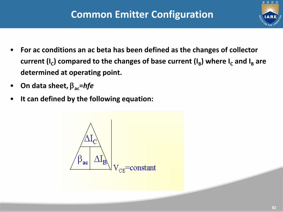
• For ac conditions an ac beta has been defined as the changes of collector
current (IC) compared to the changes of base current (IB) where IC and IB are
determined at operating point.
• On data sheet, ac=hfe
• It can defined by the following equation:
92
Common Emitter Configuration

Common Base Configuration
93

94
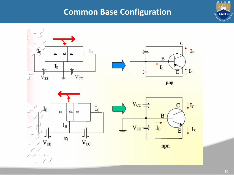
Common Base Configuration
•Common-base terminology is derived from the fact that the :- base is common
to both input and output of the configuration.
• base is usually the terminal closest to or at ground potential.
•All current directions will refer to conventional (hole) flow and the arrows in
all electronic symbols have a direction defined by this convention.
•Note that the applied biasing (voltage sources) are such as to establish current
in the direction indicated for each branch.
95
Common Base Configuration

• To describe the behavior of common-base amplifiers requires two set of characteristics:
- Input or driving point characteristics.
- Output or collector characteristics
• The output characteristics has 3 basic regions:
- Active region –defined by the biasing arrangements
- Cutoff region – region where the collector current is 0A
- Saturation region- region of the characteristics to the left of VCB = 0V
96
Common Base Configuration

97
Common Base Configuration

98
Common Base Configuration

• The curves (output characteristics) clearly indicate that a first approximation to the relationship between IE and IC in the active region is given by
IC ≈IE
• Once a transistor is in the ‘on’ state, the base-emitter voltage will be assumed to be
VBE = 0.7V
99
Common Base Configuration

Early effect
Due to forward bias, the base-emitter junction JE acts as a forward biaseddiode and due to reverse bias, the collector-base junction JC acts as areverse biased diode.
Therefore, the width of the depletion region at the base-emitter junctionJE is very small whereas the width of the depletion region at the collector-base junction JC is very large.
If the output voltage VCB applied to the collector-base junction JC is furtherincreased, the depletion region width further increases. The base region islightly doped as compared to the collector region. So the depletion regionpenetrates more into the base region and less into the collector region. As aresult, the width of the base region decreases. This dependency of basewidth on the output voltage (VCB) is known as an early effect.
If the output voltage VCB applied to the collector-base junction JC is highlyincreased, the base width may be reduced to zero and causes a voltagebreakdown in the transistor. This phenomenon is known as punch through.
100
Common Base Configuration
Transistor parameters
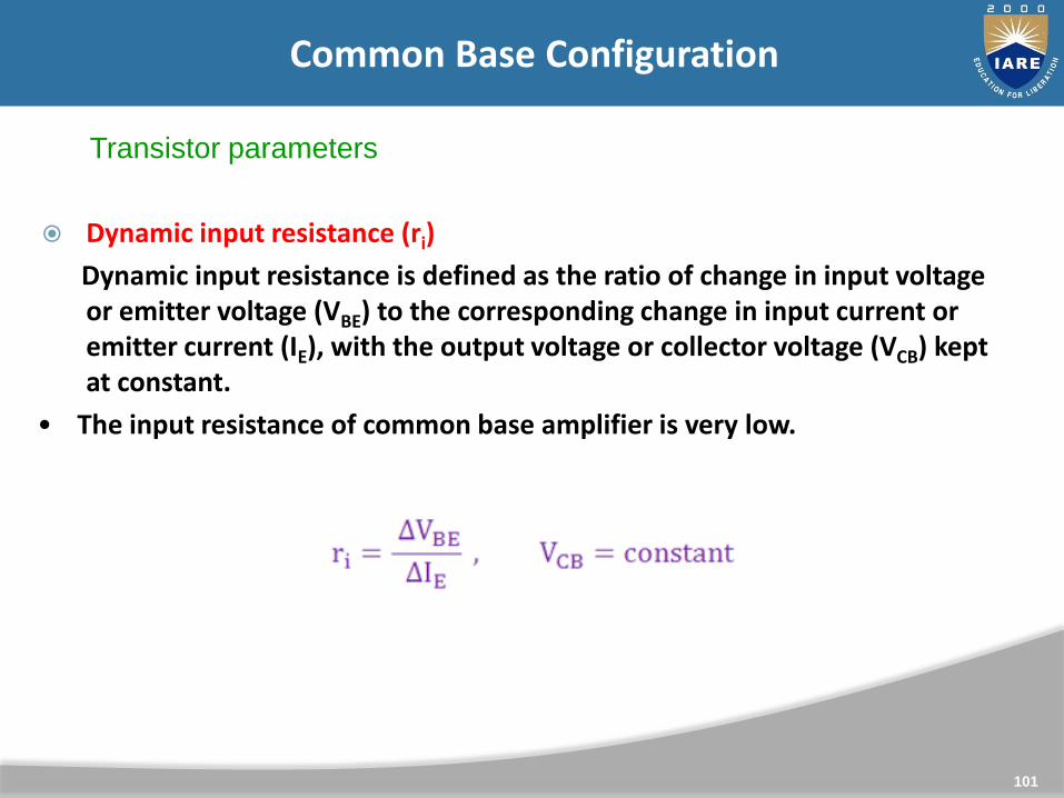
Dynamic input resistance (ri)
Dynamic input resistance is defined as the ratio of change in input voltage or emitter voltage (VBE) to the corresponding change in input current or emitter current (IE), with the output voltage or collector voltage (VCB) kept at constant.
• The input resistance of common base amplifier is very low.
101
Common Base Configuration

Dynamic output resistance (ro)
Dynamic output resistance is defined as the ratio of change in outputvoltage or collector voltage (VCB) to the corresponding change in outputcurrent or collector current (IC), with the input current or emitter current(IE) kept at constant. The output resistance of common base amplifier isvery high.
102
Common Base Configuration

103
Common Base Configuration
In the dc mode the level of IC and IE due to the majority carriers are related by a quantity called alpha
=
IC = IE + ICBO
It can then be summarize to IC = IE (ignore ICBO due to small value)
For ac situations where the point of operation moves on the characteristics curve, an ac alpha defined by
Alpha a common base current gain factor that shows the efficiency by calculating the current percent from current flow from emitter to collector. The value of is typical from 0.9 ~ 0.998.
E
C
I
I
E
C
I
I
Common – Collector Configuration
104

In this configuration, the base terminal of the transistor serves as the input, the emitter terminal is the output and the collector terminal is common for both input and output.
Hence, it is named as common collector configuration. The input is applied between the base and collector while the output is taken from the emitter and collector.
105
Common – Collector Configuration

Also called emitter-follower (EF).
It is called common-collector configuration since both the
signal source and the load share the collector terminal as a common
connection point.
The output voltage is obtained at emitter terminal.
The input characteristic of common-collector configuration is similar with
common-emitter configuration.
Common-collector circuit configuration is provided with the load resistor
connected from emitter to ground.
It is used primarily for impedance-matching purpose since it has high input
impedance and low output impedance.
106
Common – Collector Configuration

107
Common – Collector Configuration
Notation and symbols used with the common-collector configuration:
(a) pnp transistor ; (b) npn transistor.
Input characteristics
The input characteristics describe the relationship between input current or base current (IB) and input voltage or base-collector voltage (VBC).
To determine the input characteristics, the output voltage VEC is keptconstant at 3V and the input voltage VBC is increased from zero volts todifferent voltage levels. For each level of input voltage VBC, thecorresponding input current IB is noted. A curve is then drawn betweeninput current IB and input voltage VBC at constant output voltage VEC(3V).
108
Common – Collector Configuration
Next, the output voltage VEC is increased from 3V to different voltage level, say for example 5V and then kept constant at 5V. While increasing the output voltage VEC, the input voltage VBC is kept constant at zero volts.
This process is repeated for higher fixed values of output voltage (VEC).

109
Common – Collector Configuration

Output characteristics
The output characteristics describe the relationship between outputcurrent or emitter current (IE) and output voltage or emitter-collectorvoltage (VEC).
To determine the output characteristics, the input current IB is keptconstant at zero micro amperes and the output voltage VECis increased fromzero volts to different voltage levels. For each level of output voltage VEC, thecorresponding output current IE is noted. A curve is then drawn betweenoutput current IE and output voltage VEC at constant input current IB (0 μA).
In common collector configuration, if the input current or base current iszero then the output current or emitter current is also zero. As a result, nocurrent flows through the transistor. So the transistor will be in the cutoffregion. If the base current is slightly increased then the output current oremitter current also increases. So the transistor falls into the active region.If the base current is heavily increased then the current flowing through thetransistor also heavily increases. As a result, the transistor falls into thesaturation region.
110
Common – Collector Configuration

111
Common – Collector Configuration

Transistor parameters
Dynamic input resistance (ri)
Dynamic input resistance is defined as the ratio of change in input voltage orbase voltage (VBC) to the corresponding change in input current or basecurrent (IB), with the output voltage or emitter voltage (VEC) kept at constant.
The input resistance of common collector amplifier is high.
112
Common – Collector Configuration
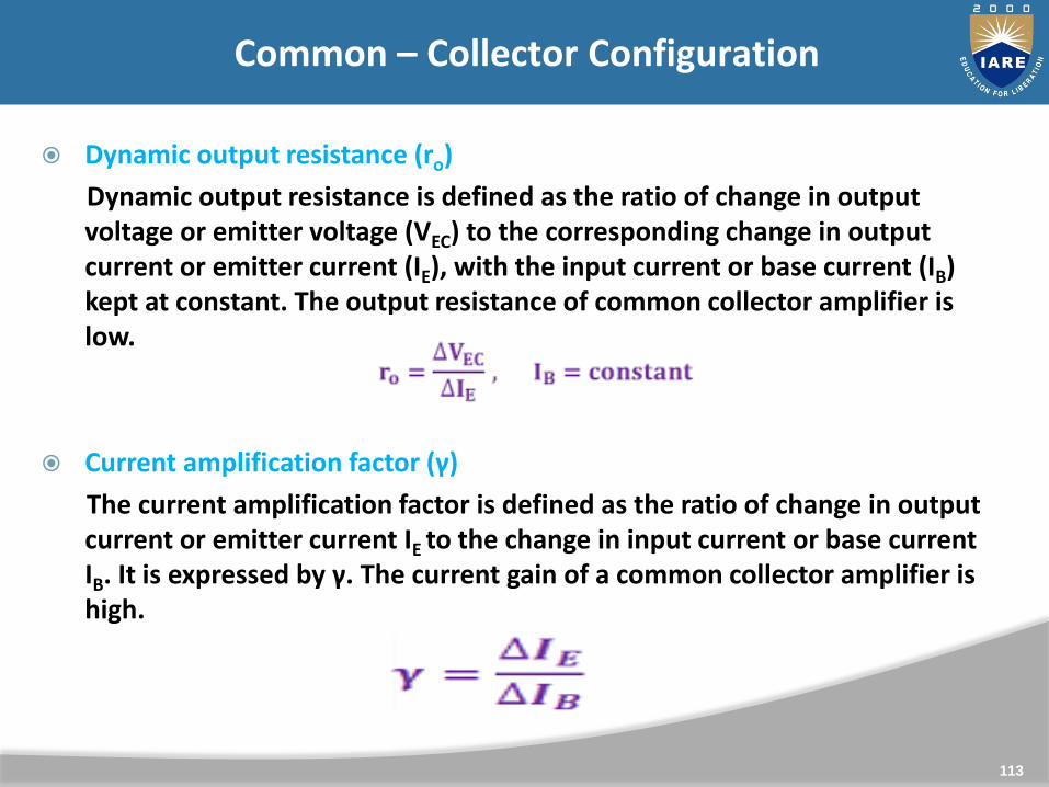
Dynamic output resistance (ro)
Dynamic output resistance is defined as the ratio of change in output voltage or emitter voltage (VEC) to the corresponding change in output current or emitter current (IE), with the input current or base current (IB) kept at constant. The output resistance of common collector amplifier is low.
Current amplification factor (γ)
The current amplification factor is defined as the ratio of change in output current or emitter current IE to the change in input current or base current IB. It is expressed by γ. The current gain of a common collector amplifier is high.
113
Common – Collector Configuration

Q point or quiescent or operating point of BJT
114

Q-point is an acronym for quiescent point. Q-point is the operating point ofthe transistor (ICQ,VCEQ) at which it is biased.
The concept of Q-point is used when transistor act as an amplifying deviceand hence is operated in active region of input output characteristics.
To operate the BJT at a point it is necessary to provide voltages andcurrents through external sources.
When a line is drawn joining the saturation and cut off points, such a linecan be called as Load line. This line, when drawn over the outputcharacteristic curve, makes contact at a point called as Operating point.
115
Q point or quiescent or operating point of BJT

Importance of q point in transistor
Normally whatever signals we want to amplify will be of the order milli volts or less.
If we directly input these signals to the amplifier they will not get amplified as transistor needs voltages greater than cut in voltages for it to be in active region.
Only in active region of operation transistor acts as amplifier. So we can establish appropriate DC voltages and currents through BJT by external sources so that BJT operates in active region and superimpose the AC signals to be amplified.
The DC voltage and current are so chosen that the transistor remains in active region for entire AC signal excursion. All the input AC signals variations happen around Q-point.
116
Q point or quiescent or operating point of BJT

C & AC load lines
DC & AC load lines
DC and AC load line
117

The dc load line is the locus of IC and VCE at which BJT remains in active region i.e. it represents all the possible combinations of IC and VCE for a given amplifier.
Procedure to draw DC load line
To draw DC load line of a transistor we need to find the saturation current and cutoff voltage.
Saturation point : The saturation current is the maximum possible current through the transistor and occurs at the point where the voltage across the collector is minimum. To find the saturation point equate the collector voltage to zero.
Cutoff point : The cutoff voltage is the maximum possible voltage across the collector and occurs at zero collector current. To find the cutoff point equate the collector current to zero.
118
DC load line

119
DC load line
From the DC equivalent circuit byapplying Kirchoff’s voltage Law incollector loop in
Vce = Vcc – Rc *Ic (Equation 1)
In equation 1 equating Ic to zero the cutoff point is (Vcc, 0).
In equation 1 equating Vce to zero the cutoff point is (0, Vcc/Rc).
DC equivalent circuit of CE amplifier

120
DC load line
(Vcc, 0) is cut off point where transistorenters in to cut off region from activeregion and (0, Vcc/Rc) is saturation pointwhere the transistor enters saturationregion.

DC load line analysis gives the variation of collector currents and voltage for static situation of Zero AC voltage.
The ac load line tells you the maximum possible output voltage swing for a given common-emitter amplifier i.e. the ac load line will tell you the maximum possible peak-to-peak output voltage Vce(cut off) from a given amplifier.
For AC input signal frequencies the biasing capacitors are chosen such that they acts as short circuits and as open circuits for DC voltages.
121
AC load line

122
AC load line
The current IC at the saturation point is
IC(sat)=ICQ+(VCEQ/rc)The voltage VCE at the cutoff point is
VCE(off)=VCEQ+ICQ*rC
AC equivalent circuit of CE amplifier

When AC and DC Loadlines are represented in agraph, it can beunderstood that they arenot identical. Both ofthese lines intersect atthe Q-point or quiescentpoint.
123
DC & AC load line

Transistor Hybrid parameter model
124

A transistor can be treated as atwo part network. The terminalbehavior of any two part networkcan be specified by the terminalvoltages V1 & V2 at parts 1 & 2respectively and current i1 and i2,entering parts 1 & 2, respectively,as shown in figure.
125
Transistor Hybrid parameter model
If the input current i1 and outputVoltage V2 are takes as independentvariables, the input voltage V1 andoutput current i2 can be written as
V1 = h11 i1 + h12 V2
i2 = h21 i1 + h22 V2

The four hybrid parameters h11, h12, h21 and h22 are defined as follows.
• h11 = [V1 / i1] with V2 = 0
= Input Impedance with output voltage short circuited.
• h22 = [i2 / V2] with i1 = 0
= Output admittance with input current open circuited.
• h12 = [V1 / V2] with i1 = 0
= reverse voltage transfer ratio with input current open circuited.
• h21 = [i2 / i1] with V2 = 0
= Forward current gain with output voltage short circuited.
126
Transistor Hybrid parameter model

The dimensions of h – parameters are as follows:
h11 - Ω
h22 – mhos
h12, h21 – dimension less.
→ as the dimensions are not alike, (ie) they are hybrid in nature, and these parameters are called as hybrid parameters.
i= 11 = input ; o= 22 = output ;
f = 21 = forward transfer ; r = 12 = Reverse transfer.
127
Transistor Hybrid parameter model

The Hybrid Model for Two-port Network
128
Transistor Hybrid parameter model

Use of h – parameters to describe a transistor has the following advantages.
h – Parameters are real numbers up to radio frequencies.
They are easy to measure
They can be determined from the transistor static characteristics curves.
They are convenient to use in circuit analysis and design.
Easily convert able from one configuration to other.
Readily supplied by manufactories.
129
Transistor Hybrid parameter model

130
Transistor Hybrid parameter model

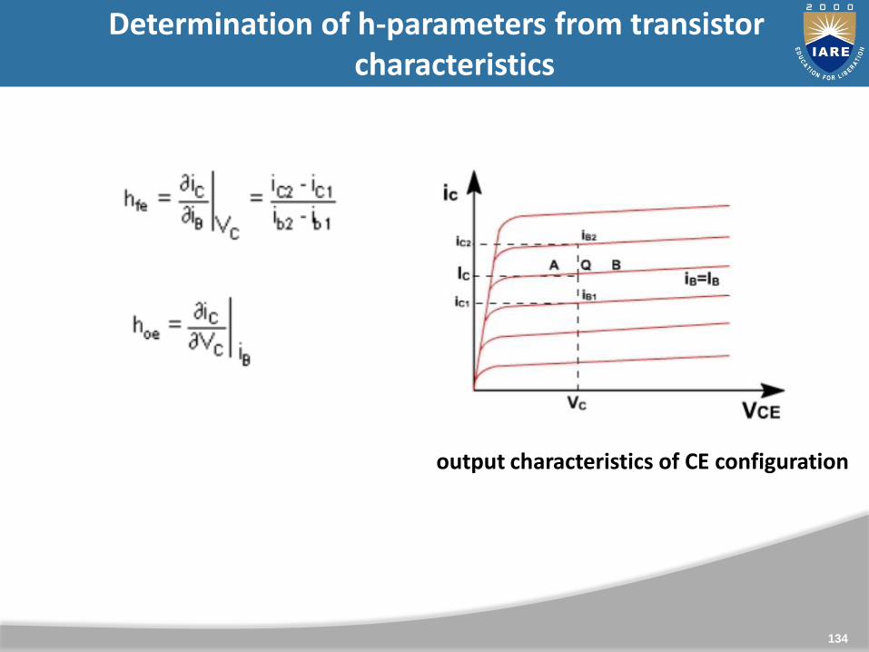
Determination of h-parameters from transistor characteristics
131

To determine the four h-parameters of transistor amplifier, inputand output characteristic are used.
Input characteristic depicts the relationship between inputvoltage and input current with output voltage as parameter.
The output characteristic depicts the relationship between outputvoltage and output current with input current as parameter.
132
Determination of h-parameters from transistor characteristics

133
Determination of h-parameters from transistor characteristics
input characteristics of CE configuration
134
Determination of h-parameters from transistor characteristics
output characteristics of CE configuration

Conversion of h-parameters
135

136
Value of h-parameters of a Typical Transistor
137
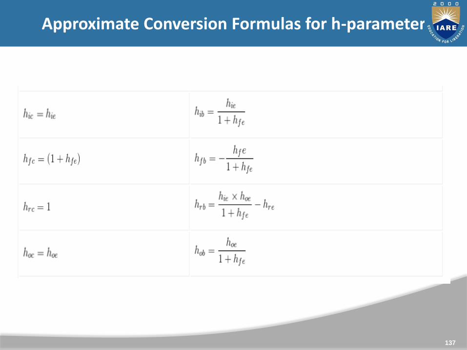
Approximate Conversion Formulas for h-parameter

PROBLEMS
138
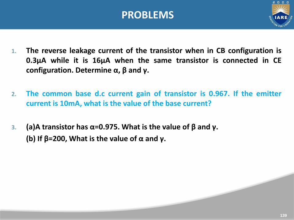
1. The reverse leakage current of the transistor when in CB configuration is0.3µA while it is 16µA when the same transistor is connected in CEconfiguration. Determine α, β and γ.
2. The common base d.c current gain of transistor is 0.967. If the emittercurrent is 10mA, what is the value of the base current?
3. (a)A transistor has α=0.975. What is the value of β and γ.
(b) If β=200, What is the value of α and γ.
139
PROBLEMS

4. A transistor has β=150. Calculate the approximate collector and basecurrents if the emitter current is 10mA.
5. A transistor has IB=105 µA and IC=2.05mA. Find
(a)β of the transistor
(b)α of the transistor
(c)emitter current IE
(d)Now, if IB changes by 27 µA and IC changes by 0.65mA,find the newvalue of β.
140
PROBLEMS

6. A certain transistor has α=0.98,IC0= 5 µA and IB=100 µA. Find the values ofcollector and emitter currents.
7. A certain transistor has α of 0.98 and a collector leakage current IC0 of 1µA. Calculate the collector and base currents, when IE= 1 mA.
141
PROBLEMS

1. What is the saturation currentand the cut-off for this circuit?Assume VCE=0.2V insaturation.
2. Is the transistor saturated?
142
PROBLEMS
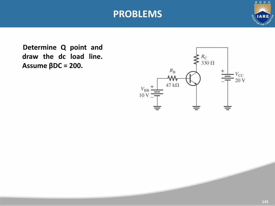
Determine Q point anddraw the dc load line.Assume βDC = 200.
143
PROBLEMS

UNIT-IIITRANSISTOR BIASING AND STABILIZATION

Outline
145
Bias Stability
Fixed Bias
Collector to Base bias
Self Bias
Bias Compensation using Diodes and Transistors
Analysis of CE, CC, CB Amplifiers
Analysis of CE Amplifier with emitter resistance
low frequency response of BJT Amplifiers
effect of coupling and bypass capacitors on CE Amplifier
Problems

Bias Stability
146

BiasingThe proper flow of zero signal collector current and the maintenance of proper collector emitter voltage during the passage of signal is known as Transistor Biasing. The circuit which provides transistor biasing is called as Biasing Circuit.
Need for DC biasing
If a signal of very small voltage is given to the input of BJT, it cannot beamplified. Because, for a BJT, to amplify a signal, two conditions have to bemet.
The input voltage should exceed cut-in voltage for the transistor to be ON.
The BJT should be in the active region, to be operated as an amplifier.
147
Transistor Biasing

The main factor that affect the operating point is the temperature. Theoperating point shifts due to change in temperature.
As temperature increases, the values of ICE, β, VBE gets affected.
ICBO gets doubled (for every 10o rise)
VBE decreases by 2.5mv (for every 1o rise)
So the main problem which affects the operating point is temperature.Hence operating point should be made independent of the temperature soas to achieve stability. To achieve this, biasing circuits are introduced.
148
Factors affecting the operating point

A transistor can work as amplifier, only if the dc/ac voltages and currents inthe circuit are suitably fixed. The operating point or bias point or quiescentpoint(or simply Q-point) is the voltage or current which, when applied to adevice, causes it to operate in a certain desired fashion. Need for biasstabilization.
Need for BIAS STABILIZATION
After fixing the operating point suitably, it should remains there only. Butthere are two reasons for the operating point to shift.
The transistor parameters such as VBE & β changes from device to device
Transistor parameters are also temperature dependent. Since the collectorcurrent is Ic = β IB + (1+ β) Ico (β, IB and Ico are temperature dependent)
β of a transistor is strongly dependent on temperature. As temp. increases,β increases
149
Bias Stability
Stability Factor
It is understood that IC should be kept constant in spite of variations ofICBOor ICO. The extent to which a biasing circuit is successful in maintainingthis is measured by Stability factor. It denoted by S.
By definition, the rate of change of collector current IC with respect to thecollector leakage current ICO at constant β and IB is called Stability factor.
S=dIc/dIco at constant IB and β
Hence we can understand that any change in collector leakage currentchanges the collector current to a great extent. The stability factor shouldbe as low as possible so that the collector current doesn’t get affected. S=1is the ideal value.
150
Stabilization Factors

• The general expression of stability factor for a CE configuration can beobtained as under.
• Differentiating above expression with respect to IC, we get
• Hence the stability factor S depends on β, IB and IC.
151
Stabilization Factor(contd.)
0(1 )c B cI I I
1
1
SdIB
dIc

152
Stabilization Factor(contd.)

Fixed Bias
153

• The biasing circuit shown bybelow Figure has a base resistorRB connected between the baseand the VCC.
• Here the base-emitter junctionof the transistor is forwardbiased by the voltage dropacross RB which is the result of IB
flowing through it. From thefigure, the mathematicalexpression for IB is obtained as
154
Fixed Base Bias or Fixed Resistance Bias
CC BEB
B
V VI
R
155
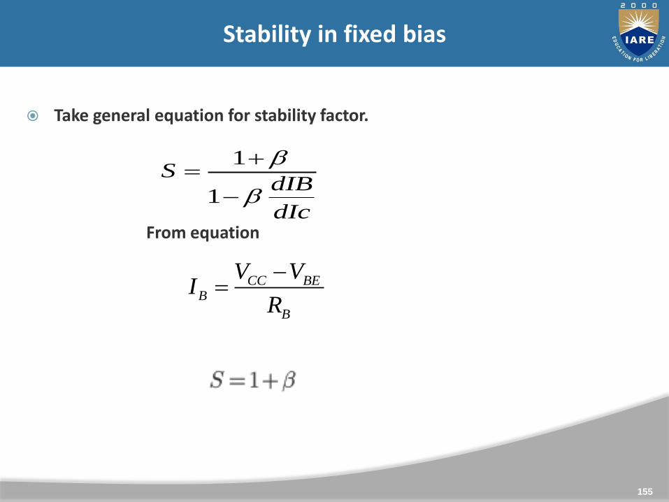
Stability in fixed bias
Take general equation for stability factor.
1
1
SdIB
dIc
CC BEB
B
V VI
R
From equation

Collector to Base bias
156

• In this circuit , the base resistorRB is connected across thecollector and the base terminalsof the transistor. This meansthat the base voltage, VB andthe collector voltage, VC areinter-dependent due to the factthat
157
Collector Feedback Bias
CCBCCC
BBCB
RIIVV
RIVV
)(

From these equations, it is seen that an increase in IC decreases VC whichresults in a reduced IB, automatically reducing IC. This indicates that, for thistype of biasing network, the Q-point (operating point) remains fixedirrespective of the variations in the load current causing the transistor toalways be in its active region regardless of β value.
Further this circuit is also referred to as self-biasing negative feedbackcircuit as the feedback is from output to input via RB. This kind of relativelysimple bias has a stability factor which is less than (β+1), which results in abetter stability when compared to fixed bias. However the action ofreducing the collector current by base current leads to a reduced amplifiergain. Here,
other voltages and currents are expressed as
158
Collector Feedback Bias
CE
BC
BEB
II
II
VV
Take general equation for stability factor
159
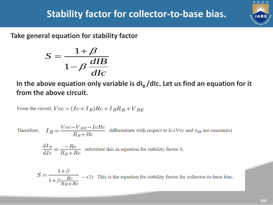
Stability factor for collector-to-base bias.
1
1
SdIB
dIc
In the above equation only variable is dIB /dIc. Let us find an equation for it from the above circuit.

Self Bias
160

A simple circuit used to establish a stable operating point is the self-biasingconfiguration. The self bias, also called as emitter bias that can be used forlow collector resistance.
The current in the emitter resistor causes a voltage drop which is in thedirection to reverse bias the emitter junction. For the transistor to remain inthe active region, the base-emitter junction has to be forward biased.
This type of biasing network employs a voltage divider formed by theresistors R1 and R2 to bias the transistor. This means that here the voltagedeveloped across R2 will be the base voltage of the transistor which forwardbiases its base-emitter junction.
In general, the current through R2 will be fixed to be 10 times required basecurrent, IB (i.e. I2 = 10IB). This is done to avoid its effect on the voltagedivider current or on the changes in β.
161
Voltage Divider Bias

Voltage Divider Bias(contd.)Voltage Divider Bias

Stabilization Factors:
To determine stability factor, S Applying Thevenin’s Theorem to the circuit
The loop equation around the base circuit can be written as
Differentiating this equation w.r.t Ic, we get
21
21
21
2
RR
RRandR
RR
VRV B
CCT
BE
E
RR
RS
1
1
ECBBEBBT RIIVRIV )(
BE
E
C
B
RR
R
dI
dI
Voltage Divider Bias

In this kind of biasing, IC is resistant to the changes in both β as well as VBE
which results in a stability factor of 1 (theoretically), the maximum possiblethermal stability.
This is because, as IC increases due to a rise in temperature, IE also increasescausing an increase in the emitter voltage VE which in turn reduces thebase-emitter voltage, VBE.
This results in the decrease of base current IB which restores IC to its originalvalue. The higher stability offered by this biasing circuit makes it to be mostwidely used in spite of providing a decreased amplifier gain due to thepresence of RE
164
Voltage Divider Bias

In a CE ge transistoramplifier circuit, the biasis provided by bias, i.e.emitter resistor andpotential dividerarrangement. The variousparameters are Vcc=16V,Rc=3K,Re=2K,R1=56K,R2=20K and α=0.985.Determine (a) thecoordinates of theoperating point and (b)the stability factor S.
165
Example
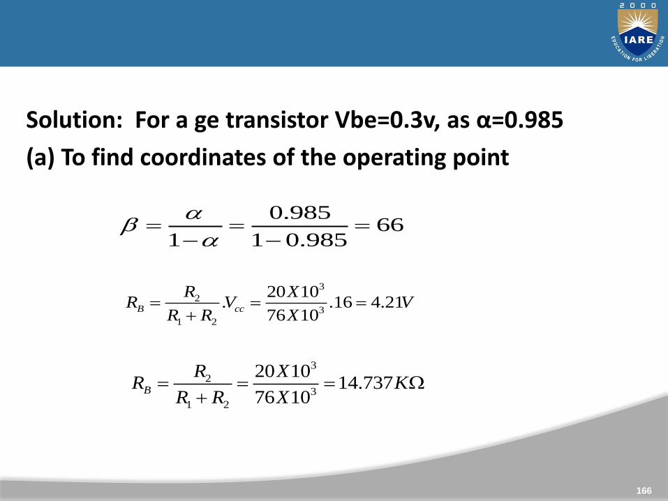
Solution: For a ge transistor Vbe=0.3v, as α=0.985
(a) To find coordinates of the operating point
166
0.98566
1 1 0.985
3
2
3
1 2
20 10. .16 4.21
76 10B cc
R XR V V
R R X
3
2
3
1 2
20 1014.737
76 10B
R XR K
R R X

The loop equation around the base circuit is
167
( )T B B BE B C EV I R V I I R
33.91 [0.223 2.03].10CI
1.73cI mA
7.35CE CC c c E EV V I R I R V
(b) To find the stability factor S,
1
(1 ).
1
B
E
B
E
R
RS
R
R
14.7371
2(1 66).14.737
1 662
S

Bias Compensation using Diodes and Transistors
168

Diode Compensation for Instability:
These are the circuits, as the gain of the amplifier is a very importantconsideration, some compensation techniques are used to maintainexcellent bias and thermal stabilization.
These are the circuits that implement compensation techniques usingdiodes to deal with biasing instability. The stabilization techniques refer tothe use of resistive biasing circuits which permit IB to vary so as to keepIC relatively constant.
There are two types of diode compensation methods. They are −
Diode compensation for instability due to VBE variation
Diode compensation for instability due to ICO variation
169
Bias Compensation techniques
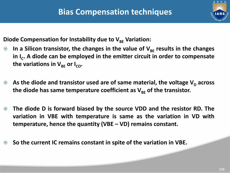
Diode Compensation for Instability due to VBE Variation:
In a Silicon transistor, the changes in the value of VBE results in the changesin IC. A diode can be employed in the emitter circuit in order to compensatethe variations in VBE or ICO.
As the diode and transistor used are of same material, the voltage VD acrossthe diode has same temperature coefficient as VBE of the transistor.
The diode D is forward biased by the source VDD and the resistor RD. Thevariation in VBE with temperature is same as the variation in VD withtemperature, hence the quantity (VBE – VD) remains constant.
So the current IC remains constant in spite of the variation in VBE.
170
Bias Compensation techniques

171
Bias Compensation techniques
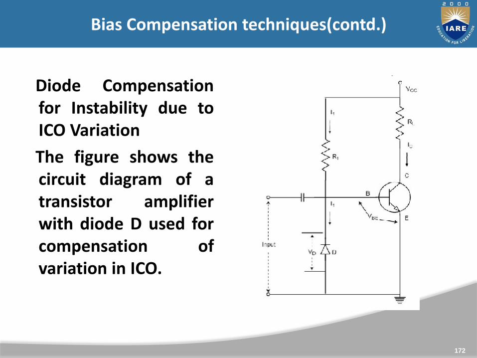
Diode Compensationfor Instability due toICO Variation
The figure shows thecircuit diagram of atransistor amplifierwith diode D used forcompensation ofvariation in ICO.
172
Bias Compensation techniques(contd.)

So, the reverse saturation current IO of the diode will increase withtemperature at the same rate as the transistor collector saturation currentICO.
173
Bias Compensation techniques
tconsR
CC
R
BEV
CC tanVV
I
The diode D is reverse biased by VBE and the current through it is thereverse saturation current IO.
Now the base current is,0IIIB
Substituting the above value in the expression for collector current.
COOC ß)I+(1+)I-ß(I=I
If β ≫ 1,COOC ßI+ßI-ßI=I
I is almost constant and if IO of diode and ICO of transistor trackeach other over the operating temperature range, then IC remainsconstant.

Analysis of CE, CC, CB Amplifiers
174
General ModelGeneral Model

1I
IA L
i
212 VhIhI of
LRIV 22
)( 212 Lof RIhIhI
122 )( IhRIhI fLo
Lo
f
Rh
h
I
I
11
2
Lo
f
Rh
h
I
I
11
2
Current gain:
General Model

ss
isI
I
I
I
I
IA 1
1
22 .
s
iI
IA 1.
si
ss
RZ
RII
1
si
siis
RZ
RAA
Current gain(Ais):
Input Resistance(Zi):
s
is
i VZR
ZV
1
1
1
I
VZi
1
211
I
VhIhV ri
Li RIAV 12
Lirii RAhhZ
General Model

Voltage Gain(Av):1
2
V
VAv
i
Liv
Z
RIAA 1
ss
vsV
V
V
V
V
VA 1
1
22
Voltage Gain(Avs):
s
vvsV
VAA 1.
s
is
i VZR
ZV
1
i
Lip
Z
RA
P
pA
2
1
2
is
Livs
RR
RAA
General Model
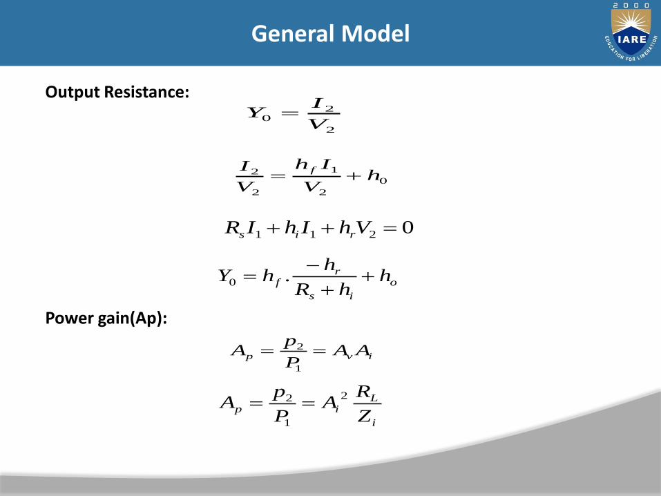
Output Resistance:
2
20
V
IY
0
2
1
2
2 hV
Ih
V
I f
0211 VhIhIR ris
o
is
rf h
hR
hhY
.0
Power gain(Ap):
ivp AAP
pA
1
2
i
Lip
Z
RA
P
pA
2
1
2
General Model
180
General Model
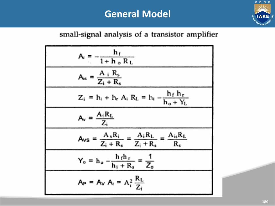
H-parameter model:
Current gain:
Loe
fe
Rh
h
I
I
11
2
Input Resistance: Lireiei RAhhZ
Voltage Gain:i
Liv
Z
RIAA 1
Output Resistance: oe
ies
refe h
hR
hhY
.0
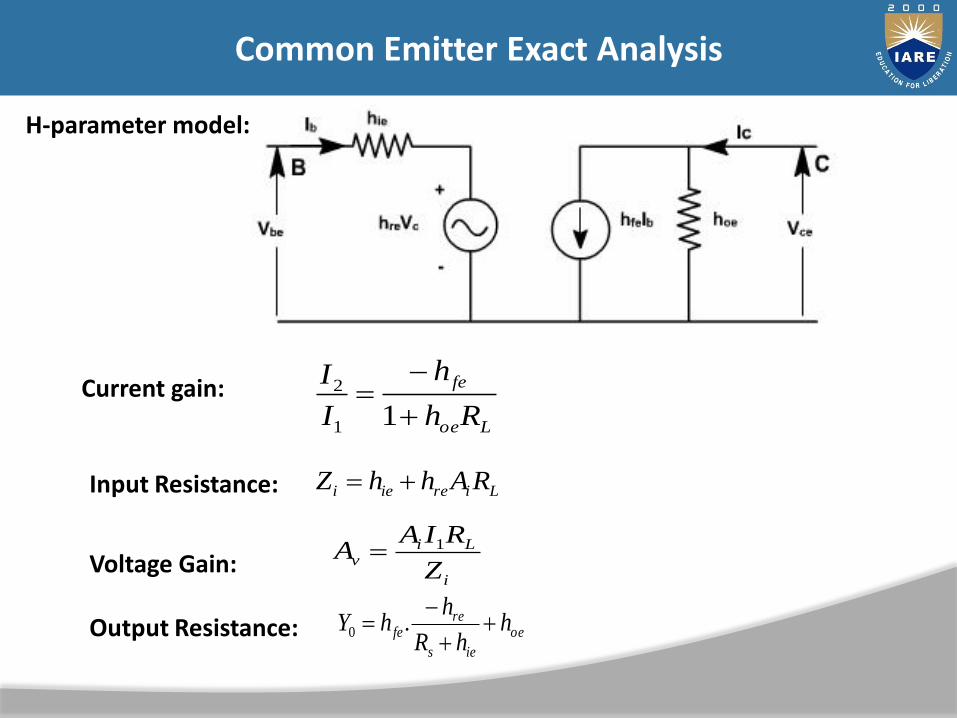
Common Emitter Exact Analysis

182
Common Base Exact Analysis
Current gain:
Input Resistance:
Voltage Gain:
Output Resistance:

183
Common Collector Exact Analysis

Analysis of CE Amplifier with emitter resistance
184

RE is added to stabilize the gain of the amplifier
RE acts as a feedbackresistor
The overall gain will reduce with unbypassedRE
Analysis Of CE Amplifier With Unbypassed RE

AC Equivalent Circuit For CE Amplifier with Unbypassed RE

AC Equivalent Circuit For CE Amplifier with RE Splitted using dual of Miller ’s Theorem

h-Parameter Equivalent Circuit (Exact Analysis)

low frequency response of BJT Amplifiers
189

190
Defining the Low Cutoff Frequency
In the low-frequency region of thesingle-stage BJT or FET amplifier, it isthe RC combinations formed by thenetwork capacitors CC , CE , and Cs andthe network resistive parameters thatdetermine the cutoff frequencies
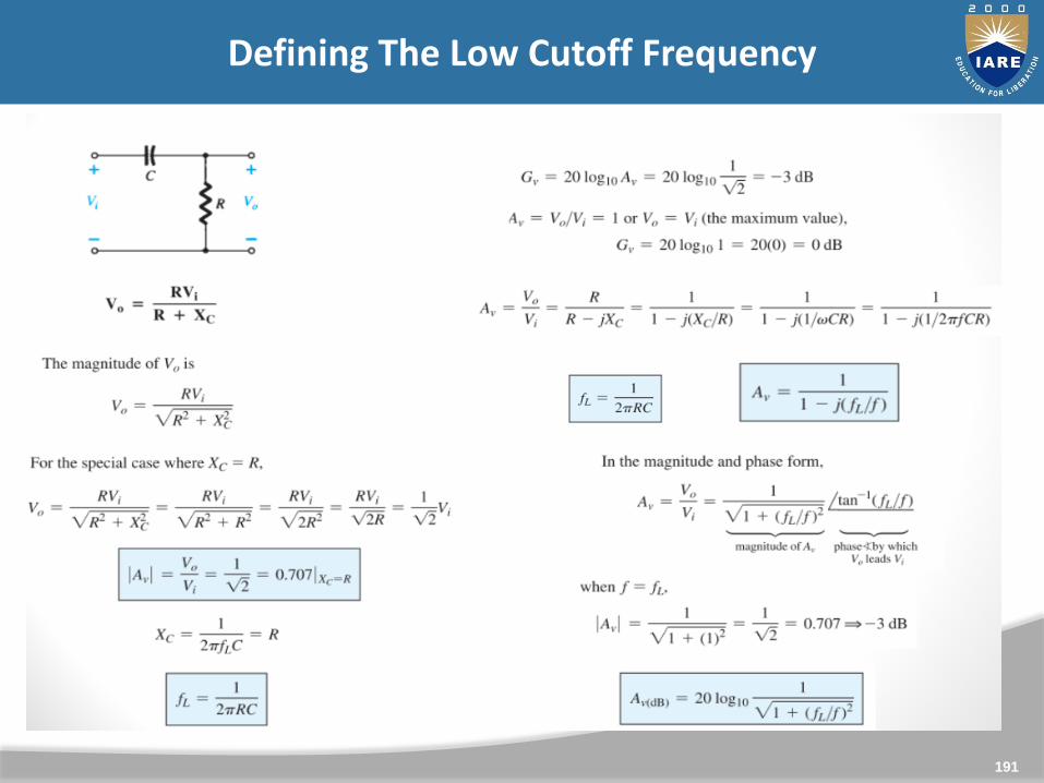
191
Defining The Low Cutoff Frequency

Effect of coupling and bypass capacitors on CE Amplifier
192

193

In general, the overall frequency response is the combination of three lowercritical frequencies due to coupling and bypass capacitors and two uppercritical frequencies due to internal capacitances.
194
The bandwidth is measured between the dominant critical frequencies.
fc1
f
Av(mid)
Av (dB)
fc2
0fc3 fc4 fc5
fcl fcu

Problems
195

1. In a Silicon transistor circuit with a fixed bias, VCC=9V, RC=3KΩ, RB=8KΩ, β= 50, VBE=0.7V. Find the operating point and Stability factor.
2. In a Silicon transistor circuit with a fixed bias, VCC=25V,
RC=820Ω, RB=180KΩ, β = 80, VBE=0.7V. Determine the values of
base current, emitter current and the collector to emitter voltage.
3. In a Silicon transistor circuit with a fixed bias, VCC=12V,
RC=330Ω,IB=0.3mA, β = 100, VBE=0.7V. Determine the value of
bias resistor RB and Stability factor.
196
Problems

4. In a Silicon transistor circuit with a collector to base bias, VCC=10V,RC=10KΩ, RB=100KΩ, β = 100, VBE=0.7V. Calculate the operating point andalso draw the load line and locate Q point on it.
5. An NPN transistor with β =50 is used in a common emitter circuit withVcc=10V,Rc=2K Ω. The bias is obtained by connecting a 100K Ω resistancefrom collector to base. Assume VBE=0.7V. Find
(a)The quiescent point
(b)The stability factor S.
197
Problems

6. Determine the quiescent currents and the collector to emitter voltage for agermanium transistor with β=50 in self biasing arrangement. Draw thecircuit with a given component values Vcc=20V,Rc=2K Ω,Re=100 Ω,R1=100KΩ,R2=5K Ω. Also find the stability factor.
7. Design a self bias circuit as per the following specifications.Vcc=12V,Vce=2V,Ic=4mA,hfe=80. Draw the complete diagram with thedesigned values.
8. The hybrid parameters for a transistor used in CE configuration are hie =5kΩ; hfe = 180; hre = 1.25 × 10⁻⁴; hoe = 16 × 10-6 ohms. The transistor hasa load resistance of 20 KΩ in the collector and is supplied from a signalsource of resistance 5 KΩ. Compute the value of input impedance, outputimpedance, current gain and voltage gain.
198
Problems

Unit - IV JUNCTION FIELD EFFECT TRANSISTOR

• Construction
• Principle of Operation
• Pinch-Off Voltage
• Volt- Ampere Characteristic
• Comparison of BJT and FET
• Biasing of FET
• FET as Voltage Variable Resistor
• MOSFET Construction and its Characteristics in Enhancement and Depletion modes
TOPICS

TYPES OF FET, FET CONSTRUCTION, SYMBOL
The family of FET devices may be divided into :
• Junction FET
• Depletion Mode MOSFET
• Enhancement Mode MOSFET

FET PRINCIPLE OF OPERATION
• The gate is connected to the
source.
• Since the pn junction is reverse-
biased, little current will flow in
the gate connection. The
potential gradient established will
form a depletion layer, where
almost all the electrons

FET PRINCIPLE OF OPERATION
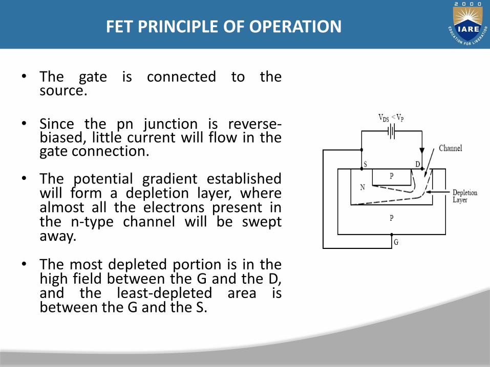
FET PRINCIPLE OF OPERATION
• The gate is connected to thesource.
• Since the pn junction is reverse-biased, little current will flow in thegate connection.
• The potential gradient establishedwill form a depletion layer, wherealmost all the electrons present inthe n-type channel will be sweptaway.
• The most depleted portion is in thehigh field between the G and the D,and the least-depleted area isbetween the G and the S.

FET PRINCIPLE OF OPERATION

• The output characteristics of an n-channel JFET with the gate short-circuited to the source.
• The initial rise in ID is related to thebuildup of the depletion layer as VDSincreases.
• The curve approaches the level of thelimiting current IDSS when ID begins tobe pinched off.
• The physical meaning of this termleads to one definition of pinch-offvoltage, VP , which is the value of VDSat which the maximum IDSS flows.
FET V-I CHARACTERISTICS

FET V-I CHARACTERISTICS
FET

• Beyond VDS = VP, there is ashort pinch- off channel oflength, ℓpo.
• As VDS increases, most ofadditional voltage simplydrops across as thisregion is depleted of carriersand hence highly resistive.
• Voltage drop across channellength, Lch remain as VP.
• Beyond pinch-off thenID = VP/RAP
(VDS>VP)
FET V-I CHARACTERISTICS

FET PARAMETERS
Forward transfer conductance, gm ofJFETs is the changes in ID based onchanges in VGS with VDS is constant.
Forward transfer conductancereferred to as gm = ∆ID /∆VGS.
Unit is Siemens (s)
The value is larger at the top of thecurve (near VGS=0) but becomesmaller as you increase VGS (nearVGS(off)).
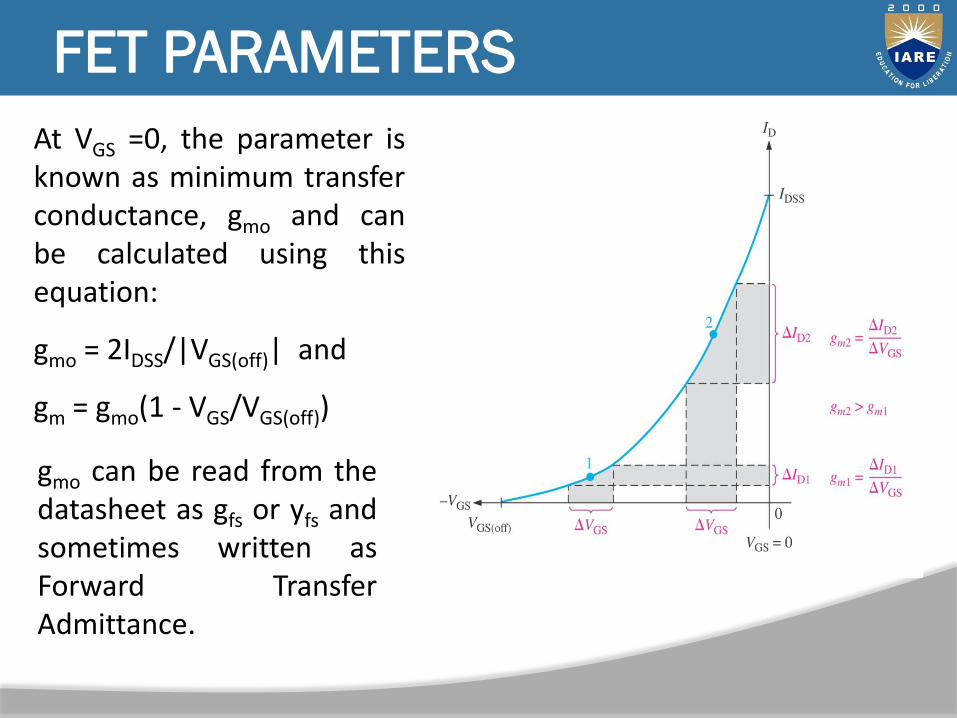
FET PARAMETERS
At VGS =0, the parameter isknown as minimum transferconductance, gmo and canbe calculated using thisequation:
gmo = 2IDSS/|VGS(off)| and
gm = gmo(1 - VGS/VGS(off))
gmo can be read from thedatasheet as gfs or yfs andsometimes written asForward TransferAdmittance.

MOSFET CONSTRUCTION AND OPERATION

MOSFET CONSTRUCTION AND OPERATION

MOSFET CONSTRUCTION AND OPERATION

MOSFET CONSTRUCTION AND OPERATION

MOSFET CONSTRUCTION AND OPERATION
An NMOS transistor with vGS > Vt and with a small vDS applied.The device acts as a conductance whose value is determinedby vGS. Specifically, the channel conductance is proportionalto vGS - Vt, and this iD is proportional to (vGS - Vt) vDS.

MOSFET CONSTRUCTION AND OPERATION
MOSFET
Depletion Type

BIASING THE FET AND MOSFET
• Biasing an FET amplifier circuit is similar to BJT amplifiers.
• The components are used external to the transistor and dc sourcesto define a predictable and stable operating point, about which thecircuit may provide linear amplification.
• Bias stability in FET amplifiers means that the dc drain current (ID)stays as constant as possible with variations in operating conditionsand device parameters.
• For the FET to operate as a linear amplifier, the Q-point should bein the middle of the saturation region, the instantaneous operatingpoint must at all times be confined to the saturation region, andthe input signal must be kept sufficiently small.

BIASING THE FET AND MOSFET
• Discrete-component biasing using source-resistance feedback isillustrated in the figure. Although the circuit is shown with anenhancement MOSFET, this biasing arrangement works fordepletion MOSFETs and JFETs.
• Note that if two supplies (VDD and –VSS) are used instead of thesingle-supply illustrated, all derived expressions will use VDD-VSS,rather than VDD.
• For depletion mode MOSFETs or JFET devices, R2 can be eitherfinite or infinite (open). To start with, we are also going to use theassumption that capacitors used in the circuit are large enough toprovide dc isolation and act as shorts under ac conditions (the old“infinite and ideal” ploy).

BIASING THE FET AND MOSFET

BIASING THE FET AND MOSFET
• Looking at the figure above, we have three unknown variables todefine for biasing (IDQ, VGSQ and VDSQ), so we need three dcequations. The first is found from the definition of the draincurrent in the saturation region, while the other two are the KVLequations obtained from the Thevenin equivalent circuit.

Unit - V FET AMPLIFIERS

222
UNIT-V
Small Signal Model, Analysis of CS, CD, CG JFET AmplifiersBasic Concepts of MOSFET AmplifiersSpecial Purpose Devices: Zener Diode – CharacteristicsVoltage RegulatorPrinciple of Operation - SCRTunnel diodeUJTVaractor Diode

223
INTRODUCTION TO JFET
FET has three terminals.
1.Drain (d) 2.source (s) 3.gate(g)
The gate is the control input.
There are 3 basic FET circuit configurations:
i)Common Source.
ii)Common Drain.
iii)Common Gate.
224
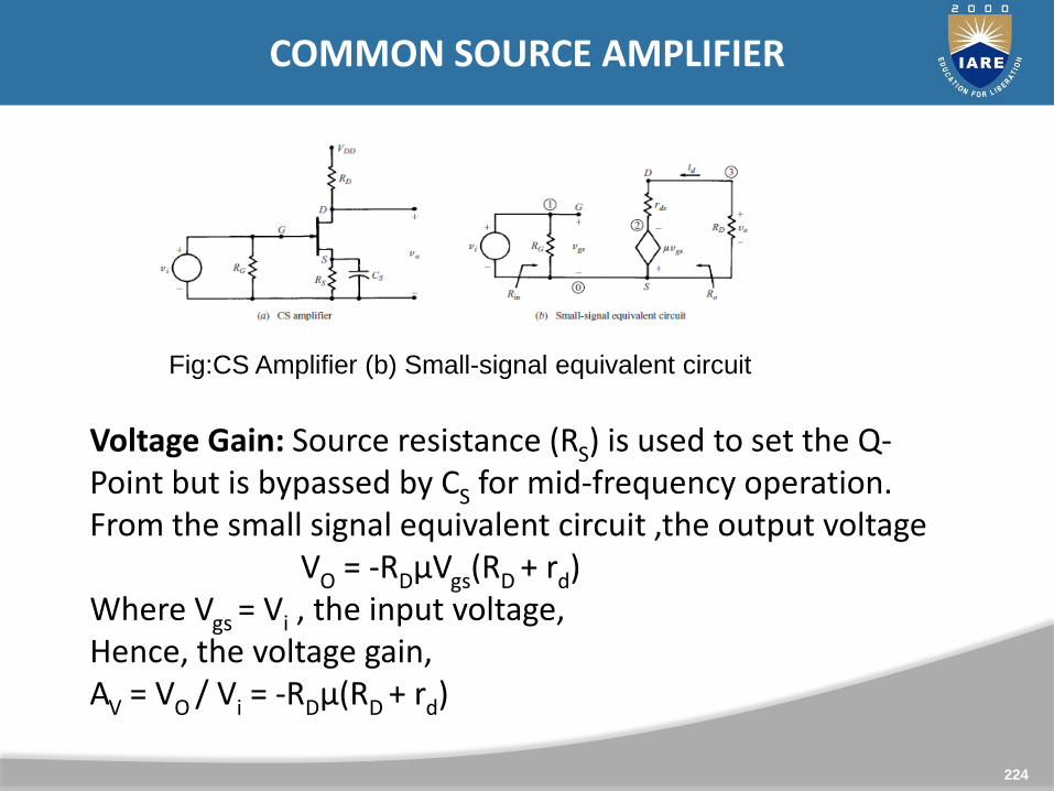
COMMON SOURCE AMPLIFIER
Fig:CS Amplifier (b) Small-signal equivalent circuit
Voltage Gain: Source resistance (RS) is used to set the Q-Point but is bypassed by CS for mid-frequency operation. From the small signal equivalent circuit ,the output voltage
VO = -RDµVgs(RD + rd)Where Vgs = Vi , the input voltage,Hence, the voltage gain,AV = VO / Vi = -RDµ(RD + rd)

225
COMMON SOURCE AMPLIFIER
Input Impedance:From Fig. Input Impedance is
Zi = RG
For voltage divider bias as in CE Amplifiers of BJTRG = R1 R2
Output Impedance:Output impedance is the impedance measured at the output terminals with the input voltage Vi = 0.when the input voltage Vi = 0, Vgs = 0 and hence µ Vgs = 0Output impedance Zo = rd RD
Normally rd will be far greater than RD . Hence Zo ≈ RD

226
COMMON DRAIN AMPLIFIER
In electronics, a common-drain amplifier, also known as a source follower, is one of three basic single-stage field effect transistor (FET) amplifier , typically used as a voltage buffer. ... That resistance reduction makes the combination a more ideal voltage source.

227
COMMON DRAIN AMPLIFIER
Voltage Gain:The output voltage,
VO = RSµVgd / (µ + 1) RS + rd
Where Vgd = Vi the input voltage. Hence, the voltage gain, Av = VO / Vi = RSµ / (µ + 1) RS + rd
Input Impedance:Input Impedance Zi = RG
Output Impedance:Output impedance measured at the output terminals with input voltage Vi = 0 can be calculated from the equivalent circuit.As Vi = 0: Vgd = 0: µvgd / (µ + 1) = 0Output Impedance: ZO = rd / (µ + 1) RS
When µ » 1 ZO = ( rd / µ) RS = (1/gm) RS

228
Types of FETs
There are two main types of FETS. They are JFET and MOSFET.

229
Construction of MOSFET
The construction of a MOSFET is a bit similar to the FET. An oxide layer is deposited on the substrate to which the gate terminal is connected. This oxide layer acts as an insulator (sio2 insulates from the substrate), and hence the MOSFET has another name as IGFET. In the construction of MOSFET, a lightly doped substrate, is diffused with a heavily doped region. Depending upon the substrate used, they are called as P-type and N-type MOSFETs.

230
V-I CHARACTERISTICS OF MOSFET
A MOSFET device has three different regions of operation. These regions are called the: Ohmic/Triode region, Saturation/Linear region and Pinch-off point. Therefore if we apply a small AC signal which is superimposed on to this DC bias at the gate input, then the MOSFET will act as a linear amplifier.

231
MOSFET AS SWITCH
CUT-OFF CHARACTERIOSTICS:The input and Gate are grounded ( 0V )• Gate-source voltage less than threshold voltage VGS < VTH
• MOSFET is “OFF” ( Cut-off region )• No Drain current flows ( ID = 0 Amps )• VOUT = VDS = VDD = ”1″• MOSFET operates as an “open switch”

232
MOSFET AS SWITCH
SATURATION CHARACTERIOSTICS:The input and Gate are connected to VDD.
• Gate-source voltage is much greater than threshold voltage VGS > VTH.
• MOSFET is “ON” ( saturation region )• Max Drain current flows( ID = VDD /RL )• VDS = 0V (ideal saturation)• Min channel resistance RDS(on) < 0.1Ω• VOUT = VDS ≅ 0.2V due to RDS(on)
• MOSFET operates as a low resistance “closed switch”.

233
SMALL-SIGNAL OPERATION OF MOSFET

234
SMALL-SIGNAL OPERATION OF MOSFET

235
SMALL-SIGNAL OPERATION OF MOSFET
the BJT small signal equivalent circuit
236
FET as common source amplifier

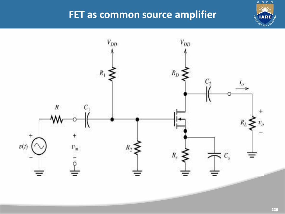
237
FET as common source amplifier
• In electronics, a common-source amplifier is one of three basic
single-stage field-effect transistor. FET amplifier topologies,
typically used as a voltage or transconductance amplifier.
• A common-drain amplifier is one in which the input signal is
applied to the gate and the output is taken from the source,
making the drain common to both. Because it is common, there is
no need for a drain resistor. A common-drain amplifier is also
called a source-follower.

238
High frequency model of MOSFET
• The MOSFET's internal capacitances limit the high-frequencyperformance of the MOSFET that means:
Limit the switching speed of the circuits in digital applications Limit the frequency at which useful amplification can be
obtained in the amplifiers.

239
ZENER DIODE
• A heavily doped semiconductor diode which is designed to
operate in reverse direction is known as the Zener diode.
• A Zener diode is a type of diode that allows current to flow
not only from its anode to its cathode, but also in the
reverse direction, when the Zener voltage is reached.
• Zener diodes have a highly doped p–n junction.
• When the diode is connected in forward bias diode acts as
a normal diode. When the reverse bias voltage is greater
than a predetermined voltage then the Zener breakdown
voltage occurs.

240
ZENER DIODE
This curve shows that the Zener diode, when connected in forwarding bias, behaves like an ordinary diode. But when the reverse voltage applies across it and the reverse voltage rises beyond the predetermined rating, the Zener breakdown occurs in the diode.

241
ZENER DIODE AS VOLTAGE REGULATOR
• A zener diode is always operated in its reverse biased condition.• A voltage regulator circuit can be designed using a zener
diode to maintain a constant DC output voltage across the load in spite of variations in the input voltage or changes in the load current.

242
Principle of operation of SCR
A Silicon-Controlled Rectifier, or SCR, is essentially a Shockley diode with an extra terminal added. This extra terminal is called the gate, and it is used to trigger the device into conduction (latch it) by the application of a small voltage.
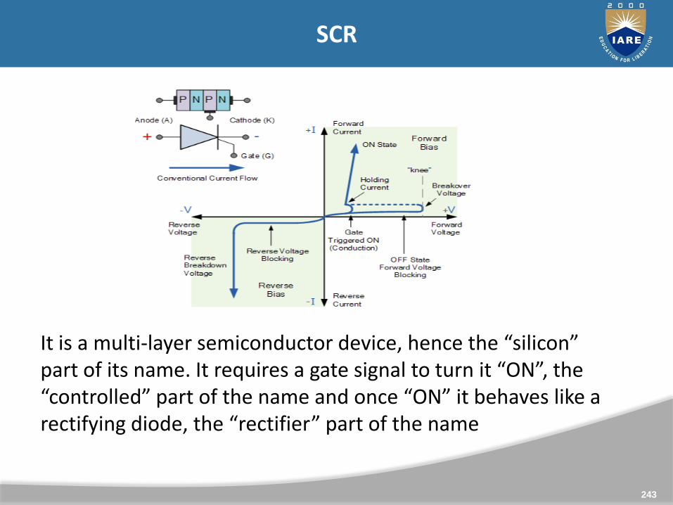
243
SCR
It is a multi-layer semiconductor device, hence the “silicon” part of its name. It requires a gate signal to turn it “ON”, the “controlled” part of the name and once “ON” it behaves like a rectifying diode, the “rectifier” part of the name

244
APPLICATIONS OF SCR
1. AC voltage stabilizers.
2. switch.
3. choppers.
4. inverters.
5. power control.
6. DC circuit breaker.
245
TUNNEL DIODE
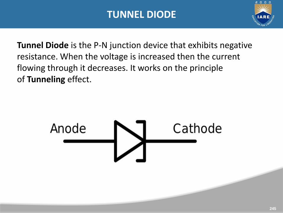
Tunnel Diode is the P-N junction device that exhibits negative resistance. When the voltage is increased then the current flowing through it decreases. It works on the principle of Tunneling effect.

246
TUNNEL DIODE
Under the forward bias condition, as voltage increases, then current decreases and thus become increasingly misaligned, known as negative resistance.Under the reverse condition, the tunnel diode acts as a back diode or backward diode. With zero offset voltage it can act as a fast rectifier.

247
APPLICATIONS OF TUNNEL DIODE
1. Ultra high speed switch.
2. Logic memory storage device.
3. Satellite communication equipment.
4. Relaxation oscillator circuits..
5. FM receivers.
6. Modern military equipment.
248
UNIJUNCTION TRANSISTOR
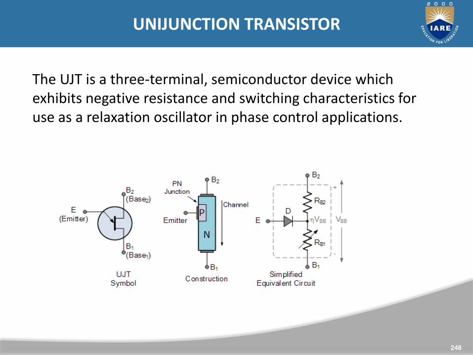
The UJT is a three-terminal, semiconductor device which exhibits negative resistance and switching characteristics for use as a relaxation oscillator in phase control applications.

249
UNI JUNCTION TRANSISTOR
• When a voltage (Vs) is firstly applied, the unijunction transistor is “OFF” and the capacitor C1 is fully discharged but begins to charge up exponentially through resistor R3.
• As the Emitter of the UJT is connected to the capacitor, when the charging voltage Vc across the capacitor becomes greater than the diode volt drop value, the p-n junction behaves as a normal diode and becomes forward biased triggering the UJT into conduction. The unijunction transistor is “ON”.
250
APPLICATIONS OF UJT
1. Relaxation oscillator.2. Voltage detector.3. Switching.4. Silicon control rectifier (SCR) and TRIAC.5. Phase control circuit.6. Timing circuit.

251
VARACTOR DIODE
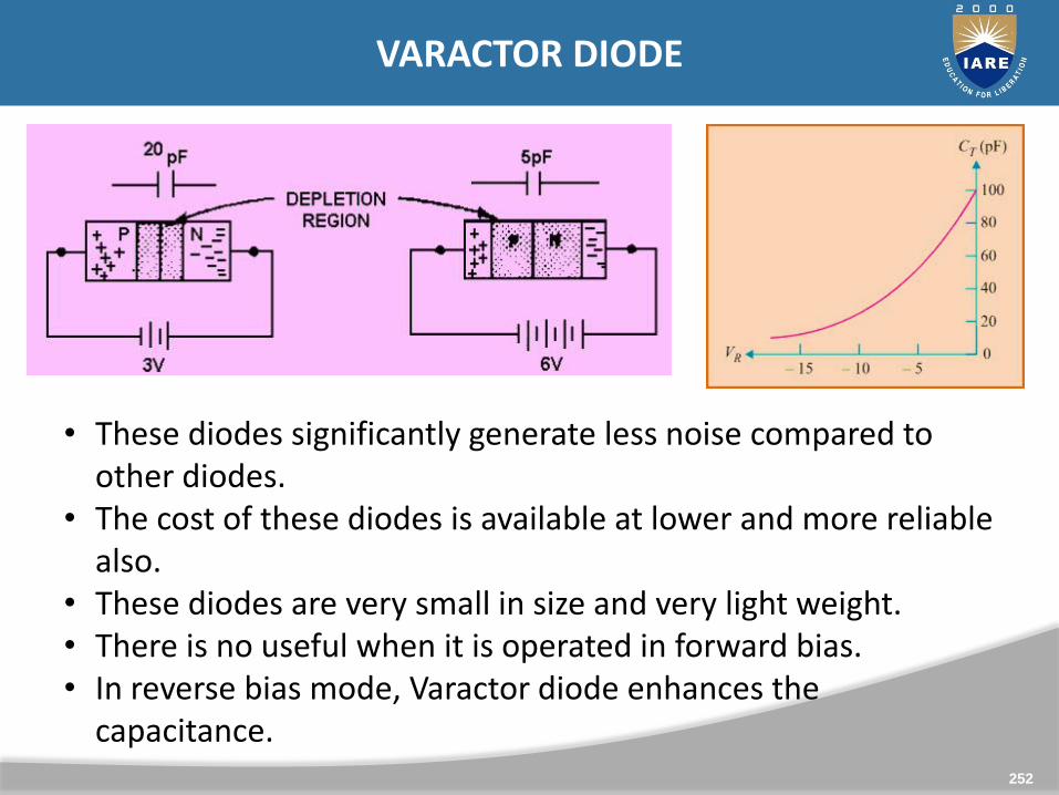
Varactor diode is a p-n junction diode whose capacitance is varied by varying the reverse voltage.
Varactor Diode is a reverse biased p-n junction diode, whose capacitance can be varied electrically. As a result these diodes are also referred to as varicaps, tuning diodes, voltage variable capacitor diodes, parametric diodes and variable capacitor diodes.
252
VARACTOR DIODE
• These diodes significantly generate less noise compared to other diodes.
• The cost of these diodes is available at lower and more reliable also.
• These diodes are very small in size and very light weight.• There is no useful when it is operated in forward bias.• In reverse bias mode, Varactor diode enhances the
capacitance.

253
APPLICATIONS OF VARACTOR DIODE
• Microwave circuits.
• Tank circuits.
• Automatic frequency controller.
• Frequency modulator.
• RF phase shifter.


