Page 1
Accelerating Sustainable Manufacturing
Copyright ©2008
SEMATECH, Inc. SEMATECH, and the SEMATECH logo are registered servicemarks of SEMATECH, Inc. International SEMATECH Manufacturing Initiative, ISMI, Advanced Materials Research Center
and AMRC are servicemarks of SEMATECH, Inc. All other servicemarks and trademarks are the property of their respective owners.
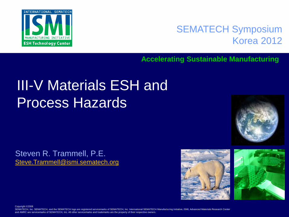
III-V Materials ESH and
Process Hazards
Steven R. Trammell, P.E. [email protected]
SEMATECH Symposium
Korea 2012
Page 2
Why Gallium Arsenide (GaAs)?
• For the 10-7nm tech node strained silicon is expected to
reach low power performance limits, requiring alternative
channel materials
• Higher electron mobility allowing functionality at higher
frequencies (i.e. faster than Si transistors)
– Applications: mobile phones, satellites
• Recent advances in processing with GaAs
– Scaling and throughput has been the historical challenge
– Recent success in layering of GaAs structures on Si substrates
• Challenges
– Introduction of thin buffer III-V materials on Si in High Volume
Manufacturing platforms
16 October 2012 2
Page 3
Overview of III-V materials
16 October 2012 3
Current elements of interest:
Ga, In, As, Sb
Coming soon:
P, others??
III-V compounds – semiconductors, PV
Other compounds – photovoltaics, etc.
Page 4
III-V material / process ESH ISMI Studies
• As / AsH3 Exposure Potential
– Operations and Maintenance
– Equipment Surface Contamination
– Exhaust and Effluents
• Process Equipment Issues
– Cross Contamination of Equipment
– Off-gassing of Post Processed Wafers
• Facility and Infrastructure Issues
– Handling of Pyrophoric Precursors, Toxic Gases, H2
– Maintenance of Support Equipment, Ducts, etc.
• Waste / Effluent Issues
– As Detection in Complex Waste Streams
– Treatment / Removal Technologies
– Solid Waste Handling
16 October 2012 4
Page 5
Arsenic and arsine exposure limits
* SEMI S-12, Section 10.1, Table 5
Exposure Limits Arsine Arsenic
- in air
Arsenic –on
Surfaces
(mg/m3) (mg/m3) (mg/100 cm2)
NIOSH REL (15 min Ceiling) 0.002 0.002 -
NIOSH Immediately Dangerous to Life
and Health (IDLH)
10
(from 3 ppm)
5 -
ACGIH TLV 0.016 0.01 -
OSHA Action Level – Continued
Monitoring Required
- 0.005 -
OSHA PEL 0.200 0.010 -
SEMI Decontamination Level* - - 0.050
16 October 2012 5
Page 6
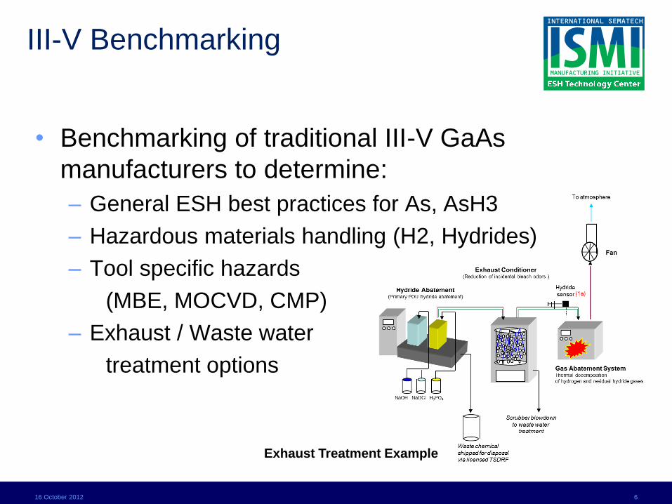
III-V Benchmarking
• Benchmarking of traditional III-V GaAs
manufacturers to determine:
– General ESH best practices for As, AsH3
– Hazardous materials handling (H2, Hydrides)
– Tool specific hazards
(MBE, MOCVD, CMP)
– Exhaust / Waste water
treatment options
16 October 2012 6
Exhaust Treatment Example
Page 7
III-V Benchmarking
16 October 2012 7
• Hazardous Materials
Handling
Materials Delivery
Example
Page 8
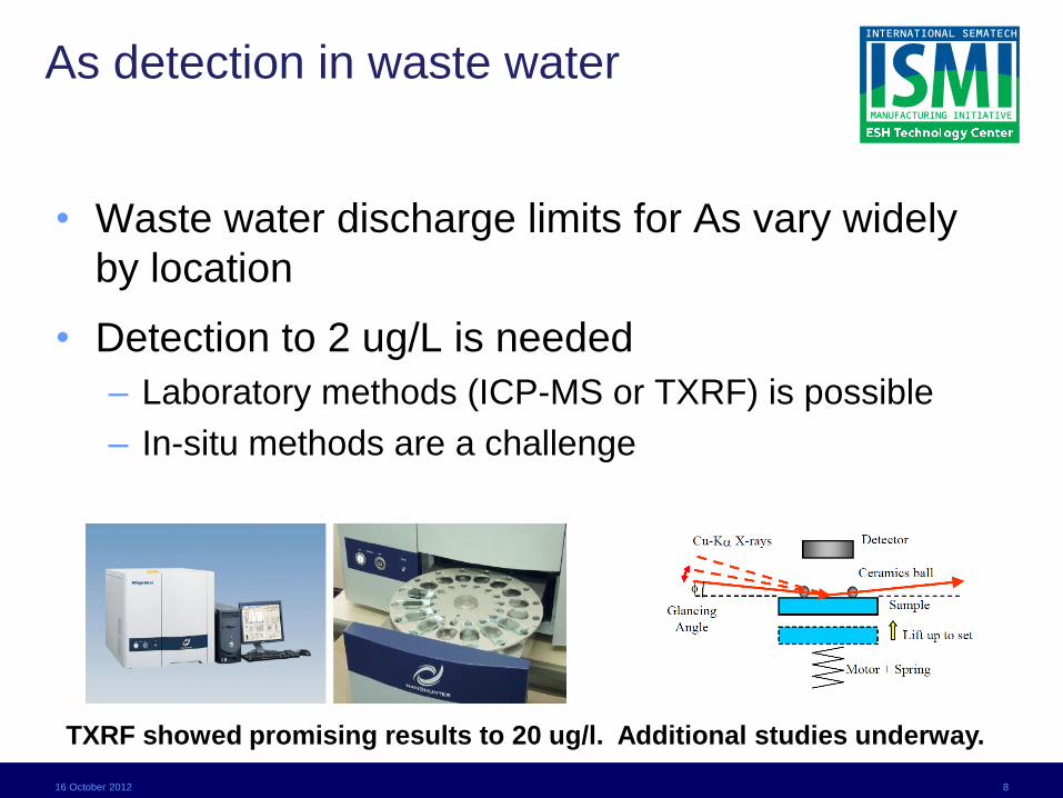
As detection in waste water
• Waste water discharge limits for As vary widely
by location
• Detection to 2 ug/L is needed
– Laboratory methods (ICP-MS or TXRF) is possible
– In-situ methods are a challenge
16 October 2012 8
TXRF showed promising results to 20 ug/l. Additional studies underway.
Page 9
Off-gassing evaluations - IMEC
16 October 2012 9
Source: IMEC
34th Annual SESHA Symposium, March 2012
Page 10
Off gassing assessment - CNSE
16 October 2012 10
Small coupons (III-V films on Si) experiments – chemistries tested are diluted HF
(50:1) and (10:1), HF and Nitric acids
60 sec dip into followed by DI rinse
Experiments carried out in an enclosed 124L glovebox – arsine concentration was
analyzed with CM4 (providing sampling flow of 3L/min with 10sec sampling
intervals)
HF or Nitric
beaker
Sealed glove box (volume : 124L)
CM4
sampling
port intake –
3L/min DI water for
rinse
1. 60sec DIP
2. Rinse
Nitrogen
purge supply
Glove box lid
Page 11
Off gassing assessment - CNSE
16 October 2012 11
Small coupons experiments – 60 sec dip into HF 10:1 followed by DI rinse in the
enclosed 124L glovebox – arsine concentration analyzed with CM4 (providing
sampling flow of 3L/min)
Preliminary Results:
Experiments Repeated For:
• Concentrated HF
• 50:1 Dilution
• Nitric Acid
• Nitric / HF mixture
Page 12
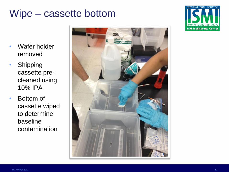
Wipe – cassette bottom
• Wafer holder
removed
• Shipping
cassette pre-
cleaned using
10% IPA
• Bottom of
cassette wiped
to determine
baseline
contamination
16 October 2012 12
Page 13
Wafer in cassette bottom
• Wafer elevated
for easy
breaking
• III-V layer on top
16 October 2012 13
Page 14
Wafer break procedure with AsH3
monitor
• Long screwdriver
inserted through
hole in cassette top
• Wafer broken with
singular, forceful
stab in middle
• Test occurred in
laboratory hood
• Exhaust from top to
bottom
16 October 2012 14
Page 15
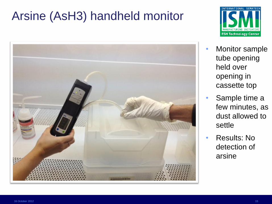
Arsine (AsH3) handheld monitor
• Monitor sample
tube opening
held over
opening in
cassette top
• Sample time a
few minutes, as
dust allowed to
settle
• Results: No
detection of
arsine
16 October 2012 15
Page 16
Broken wafer
• Wafer
shattered into
many shards,
bits and dust
16 October 2012 16
Page 17
Broken wafer bits
• Wafer bits and
dust
remaining
after dumping
shards into
waste bag
16 October 2012 17
Page 18
Post-break post-dump bits
• Photo showing
scale of wafer
dust
16 October 2012 18
Page 19
Post-break post-dump of shards wipe
• Wafer shards
dumped into
waste bag
• Wipe sample
taken of
bottom of
cassette
• Result:
16 October 2012 19
Page 20
Vacuuming box bottom
• Bits and dust
vacuumed (into
dedicated
HEPA arsenic
vacuum), from
cassette bottom
• There was not
significant
material
adhered to
cassette top
16 October 2012 20
Page 21
Post-break dump and vacuum clean
• Cassette
bottom
cleaned after
shards
dumped out
and bits and
dust
vacuumed out.
• A 2nd more
aggressive
clean was also
performed.
16 October 2012 21
Page 22
Wafer break wipe samples
analytical results (Detection Limit = 0.002 mg for Arsenic)
Tool ID/Process Activity Sample Location
As
Results
(mg)
Area
Wiped
(cm2)
Conc.
(mg/100 cm2)
Shipping Cassette Pre-Wafer Break Bottom <0.002 100 <0.002
Shipping Cassette Pre-Wafer Break Side <0.002 100 <0.002
Shipping Cassette Pre-Wafer Break Top <0.002 100 <0.002
Shipping Cassette Post-Wafer
Break Bottom 0.260 100 0.260
Shipping Cassette Post-Wafer
Break Side 0.093 100 0.093
Shipping Cassette Post-Wafer
Break Top 0.047 100 0.047
Shipping Cassette Post-Clean Bottom 0.018 100 0.018
Shipping Cassette Post-Clean Side 0.021 100 0.021
Shipping Cassette Post-2nd Clean Side <0.002 100 <0.002
Wafer Sliver Post-Break Broken Edge <0.002 <5 <0.04
* SEMI S-12, Section 10.1, Table 5 decontamination level is 0.010 mg/100 cm2
16 October 2012 22
Page 23
Wafer break study summary
• Broken wafers with GaAs layers will release measurable
amounts of arsenic as dust and small particles. – Small particles can be removed with a vacuum.
– Dust can be removed with a wet wipe, but a detailed cleaning is
necessary to remove it all.
– Respiratory protection typically not needed in ventilated/exhausted
areas.
• Edges of broken wafer shards do have measurable
amounts of arsenic. – Arsenic dust settling from wafer break is likely source
– Shards should be swept or vacuumed, or picked up by hand using
thick neoprene or equivalent gloves.
16 October 2012 23
Page 24
16 October 2012 24
http://www.ismi.sematech.org