NCLASSIFIED C DAD0-76- 0Fo fnfMENEMl0lflflmmhhlllhlllllullllllmlmlhlhu
IIIEEIIhIIIIIIlInINIIihillHE~llllhi
RESEARCH AND DEVELOPMENT TECHNICAL REPORTCORADCOM-76-0040-F99
9 MANUFACTURING METHODS AND TECHNOLOGY PROGRAM
OF INJECTION LASER DIODES FOR USE IN FIBER
OPTIC COMMUNICATIONS.
< D TICI ALBER~T GENA;O 1
LASER DIODE LABORATORIES JUL 17 198
1130 SOMERSET STREETNEW BRUNSWICK, N. J. 08901
31 MARCH 1981
FINAL REPORT FOR PERIOD JULY 1976-FEBRUARY 1981
APPROVED FOR PUBLIC RELEASE; DISTRIBUTION UNLIMITED
VMIS DOC TM~r IS BEST QUALITY PRACTICA11IMK C(lPY . rFr TO "ON, ,.bNTAINED AS G1IFICA1U IF'CATBER OF AGLS WHI C DO NM
"WRODUCE LEGIBLY.
CORADCOMi S ARMY COMMUNICATIONS RESEARCH , DEVELSP1MENT COMMAND
SFORT MONMOUTH, NEW JERSEY 07703
1 7 16 13
DISCLAIMER STATEMENT
The findings in this report are not to be construed as anofficial Department of the Army position unless so designatedby other authorized documents.
DISPOSITION INSTRUCTIONS
Destroy this report when it is no longer needed. Do notreturn it to the originator.
ACKNOWLEDGEMENT STATEMENT
This project has been accomplished as part of the U.S. ArmyManufacturing Methods and Technology Program which has as itsobjective the timely establishment of manufacturing processes,techniques, or equipment to insure the efficient productionof current or future defense programs.
l ,
_ -ix--- -
DISCLAIMER NOTICE
THIS DOCUMENT IS BEST QUALITYPRACTICABLE. THE COPY FURNISHEDTO DTIC CONTAINED A SIGNIFICANTNUMBER OF PAGES WHICH DO NOTREPRODUCE LEGIBLY.
I
T
WNCIASS IFIELDlf~lln Y ELA A1,I 'l & OF% n 4I41 P'ArI (11g.. I) F InF-,
Ir 0"ONI1PFING AGENCY FAM. I AODPFsi(II life,.nI In'm 2.ng ~ollfj OIli.. IS SFCUrFITY CLASS (.1 thl f-po1)// +, Unclassif ied
I5.. OECLASSIFI CATIONOOWNGRAOINGSCHEDULE
i6. [)ISTII4OIU ION STATEMENT
(0h Ihi. R-15-1)
Aj.provu'd for public release; distribution unlimited.
'. 0 I ST IIJI I1.J %IATFM r'I-T l the Ab.uer, entered In l rk 20). it811. r ni fle . m. Rep oI)
S 5 UPLEMN T;qY NOT
iS K1EV WOflO" f((' 4nt ne,1n r er,** .i4 if mr .. d Idenfiiy hy blok .. u.b.1)
J , j,,Cti,., LaserU DiodcsFlbrr Optic Communications(I I I i uM AluM ntim ArsenideI)( ll( , He teornjunct.ion I,aser Diode
" Jho_ desiqn and fabrication of injection laser diodes for use infih.'r opi ic communicatiions is discussed with regard to materials 1 iithcsis;, chip configuration, and device assembly in manu-f -i -tj inq environment. The opto-electronic source is based ontho ;al" -GaAIAs double heterojunction structure and consists ofd parallel array of lasers formed by the application of triplestripe geometry to the surface of the epitaxial wafer. The
DD 'J. 1413 f.')ii, IN OF INOV GS I& OBSOLETE I UN( A S TETEDSECURITY CL ASstrIC
A TION OfV 71.15 RA',7 (TH*I fl'9* F-f*n.,d)
/ ' /.,.-
f CUOI IT CL IV, A hM OfV THI PAUE £hyf4 *U.(
II1(n(Ulthic triand of discrete lasiniq elements is mounte d in af) uhl fremency package which incorporates a high qualityooici a window.
Accession For
1TIS GFArlDTIC TV
By--
Ditw>
..NCI.ASSTrrDIf -tIIY CLASIrICATIO14 OF lulPA PlM. lI*P.'S~
TABLE OF CONTENTS
Section Page
I Introduction ........ ................. 1
Ii Device Design Requirements and PerformanceSpecifications ...... ................ 2-9
2.1 Electro-Optical Characteristics ... ....... 2
2.2 Device Structure ..... ............... . 2-7
2.3 Array Configuration ...... ............. 7
2.4 Package Requirements .... ............. .7-9
III Manufacturing Methods and TechnologyEngineering ...... ................. 9-54
3.1 Material Technology ...... ............. 9
3.1.1 Synthesis of Device Structure via LPE ... 9
3.1.1.1 Liquid Phase Epitaxial System .. ........ 9-17
3.1.1.2 Growth Process for the Synthesis of DoubleHeterojunction Structures .... .......... 17-24
3.3.1 Test Equipment ...... .............. . 50-70
IV Summary of Pilot Line Test Results ........ .71-80
V Pilot Line Rate Report ................. 81-82
VI Volume Production Plan ......... 83-86
Appendix A Product Capability Demonstration .. ....... .87-94
Appendix B SCS-516 Specifications ..... ............
Appendix C Distribution List ...............
LIST OF FIGURES
Figure Page
1 Schematic Representation of the EpitaxialStructure for Fabrication of StripeGeometry Double Heterojunction InjectionLaser Diodes ........ ................. 5
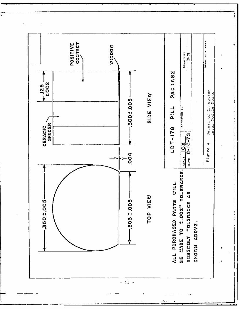
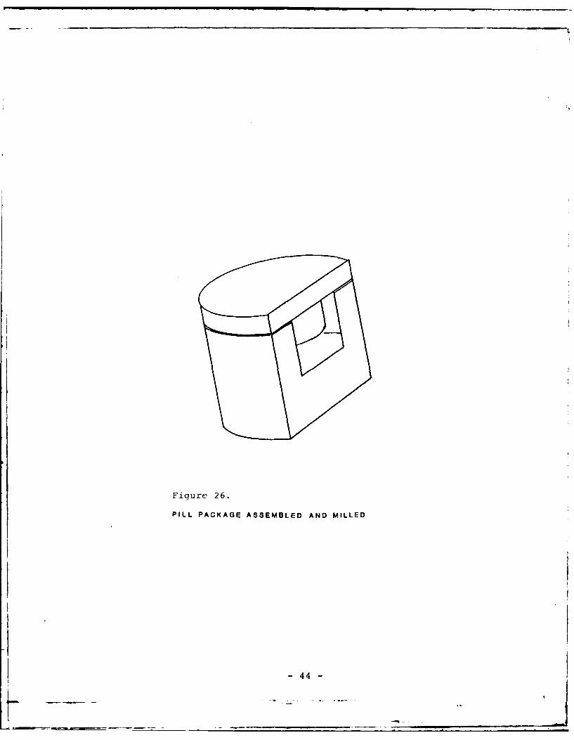
3 Outline of Laser Diode Pill Package ... ...... 10
4 Detail of Injection Laser Module Mount ....... .11
5 Block Diagram of Liquid Phase EpitaxialSystems Currently in Use at Laser DiodeLaboratories ....... ................. 13
6 Photograph of Liquid Phase EpitaxialReactors at Laser Diode Laboratories ........ .15
7 Schematic Diagram of Gas Control Subsystem. . . 16
8 Photograph of Eight Bin Ultra High Purity
Graphite Epitaxial Boat .... ............ .18
9 Sequence of Operations for Liquid PhaseEpitaxial Synthesis ....... .............. L9
10 Temperature Program Used in the LiquidPhase Epitaxial Growth of Double Hetero-junction Structures for Monolithic StripeGeometry Laser Diodes ..... ............. 22
11 Photograph of Typical Double HeterojunctionStructure Required for the Manufacture ofMonolithic Stripe Geometry Injection Laser
Diodes ........ ..................... .23
12 Surface Morphology of the As-Grown Hetero-epitaxial Wafer ...... ................ 25
13 Process Flow Diagram for the Fabricationof Monolithic Stripe Geometry InjectionLaser Arrays ........ .................. 26
14 Scribing Apparatus for Cleaving EpitaxialWafer into Slivers ..... .............. 28
ii
LTST OF FIGURES (Cont'd)
Fi( tre Page
15 Photograph of Triple Stripe GeometryApplied to Surface of an Epitaxial Wafer .... 30
16 Photograph of Individual Triple ElementModules ........ .................... 31
17 Pill Package-Mounting Base (PositiveElectrode) ....... .................. 32
Output Power 250 C 200 mw: DF=10%: t 10ns: I =3A max. 2Ap p
BURN-IN DF=10%: t =10ns; I p=2A Typ.
POST BURN-IN
Peak Wavelength 800-830nm iA=5% max. 820 nm
Output Power 250C 200 mw: DF-10%: t =i0ns: I=2A Typ. 200 mw
p
- 75 -
(0040)
CAVITY LINED WITH HARD RUBBER
DEVICES PLACED WINDOW DOWN ON RUBBER
CAVITY FILLED WITH STEEL SHOT
ACCELERATION FIXTURE
- 76 -
(004o
G/ROUP A
CON D ITTON S
TEST REQUI REMENTS __ _ TYP R-'SUTS
SUBGROUP I
Visual & Mechanical MlL-STD-750 Meth. 2071 PASS
Stripe Width 10% DF t =10 ns -
Triple 75 1m Max.
SUBGROUP 2 END POINT TESTS
Peak Wavelength 815 + 15 nm 820 nm
Peak Pulse Output Power 200mw min. - 2A Typ. 200 mw
SUBGROUP 3
Beam Width At 202mw min. at 1p
a) Junction Plane 150 13 20
b) Perpendicular to Junct. 400 38 + 20
-77-
(0(40)
GROUP B
CONDITIONS
TEST MIL-STD METHOD REQUIREMENTS TYP. RES.
SUBGROUP I
Physical 'iomensionr 750 2071 PASS
SUBGROUP 2
Thermal Shock 750 1051 A-10 cycles PASS
Moisture Resistance 750 1021 PASS
1*:nd Point Group A - Subgroup 2 NO CHANGE
SUBGROUP 3
Shock 750 2016 500g 0.5 ms PASS
Vibration Fatigue 750 2046 - PASS
Vibration, V.F. 750 2056 - PASS
Constant Acc 850 2006 10OOg 6 dir
End Point Group A - Subgroup 2
Hligh Temp. Life 850 1032 82 0 C x 340 hrs. PASS
E.nd Point Group A - Subgroup 2 NO CHANGE
SUBGROUP 5
Steady State Life
(340 Hrs) 750 1027 DF=10%t =10ns:I=2A Tye.
End Point Group A - Subgroup 2 200noW @ 2A Typ.
For First Article Subgroups 1.2 & 3 Only
- 78 -
(0040)
GROUP C
TEST MIL-STD METHOD REQUIREMENT TYP. RESULTS
SUBGROUP 1
Thermal Shock 750 1051 Al-25 cycles PASS
End Point Group A Subgroup 2 NO CHANGE
SUBGROUP 2
Solvent Resistance 202 215 PASS
End Point Group A Subgroup 2 PASS
SUBGROUP 3
Hign Temp. Life 750 1031 85'C x 1000 hrs PASS
End Point Group A Subgroup 2 NO CHANGE
SUBGROUP 4
Steady-State Life DF:10%:t :i0ns:(2000 Hrs.) 750 1026 1=3 A map. PASS
End Point Group A Subgroup 2except Pa=190 mw 200 mw
- 79 -
%CHANGE IN CURRENT
FOR 200mW OUTPUT C)u
CD
CDCDC)
C)CDC)
CD)
CDD
C)D
-~ C)
CCD
(DD(DD
CD CD
c)
C) CD 0
Cj
CDCD
Co
CD
c)0
SECTION V
PILOT LINE RATE REPORT
- 8] -
00 00 4'T In CI
U H) N - r c %
CD0 0 ,II-1 O
-4 J
U) (N ('
H IO'
04 Io 0 I
m-. I4 I,-I s:I ) 1:s4 1) r4
U)n uU0 .
(Ii C.)82
SECTION VI
MASS PRODUCTION PLAN
-83 -
-83-
~~ C'
zcr_ 0
41-
01-
U))
- r c!F
0 (Du w~
n 0 -- U)
C1.- 0 Oj I - - - - W - -U -P
w In1 - -
o MIIc
0) I I4
---- 4 -- 1I- +-4- 0- 0
w > 01 c .41 L
to I
IC'4 al
I r 85
EPITAXIAL REQUIREMENTS
Diode chips required per week 5332
Maximum number of chips per wafer 2900
Number good electrical chips per wafer 1780
Number wafers required @ 50% yield 6
EQUIPMENT REQUIREMENTS
2630 Burn-In positions @ $ 180 per position
7 Assembly Stations @ $ 2,000 per station
Epitaxial Furnace $22,000
Power Measurement T-st 2oL $10,000
PERSONNEL REQUIREMENT
Engineers 2
Technicians 2
Assembly 21
-86-
V '--im•i
INJECTION LASER DIODES FOR FIBER OPTIC COMIiKiCATIONS.(UlMAR 8 A GENNARO DAASO?-76-C-004O
CLA$SIFIED CORAOCON-?6-0040-F UL
EEEEEMONEonllllllllllll
IIIIIIIIIIIIIIIIIIIIIIIIIIIIIIIIIII
APPENDIX A
PRODUCT CAPABILITY DEMONSTRATION
-87 -
LABOATOKS. PC
DEMONSTRATION SCHEDULE
February 18, 1981
9:00 A.M. - Welcominq Session (Holiday Inn)
9:30 A.M. - Technical Presentation Program #8135
- Diode Specifications
- Diode Chip Concepts
- Packaging and Assembly Concepts
- Testing Methods
10:45 A.M. - Coffee
11:00 A.M. - Technical Presentation Program #0040
- Diode Specifications
- Diode Chip Concepts
Packaqinq and Assembly Concepts
- Testinq Methods
12:00 P.M. - Lunch
1:00 P.M. - Transport to LDL (Provided)
1:30 P.M. - Tour of LDL Facilities
- Demonstration of Diodes
2:30 P.M. -- Transport to Holiday Inn (Provided)
- 88 -
CONTRACT DAABO7-76-C-OO'40-
TRIPLE STRIPE LASER
-89-
1
U. S. ARMY CORADCOM SPECIFICATION DAAB07-76-C-0040
PRODUCT CAPABILITY DEMONSTRATION, FEBRUARY 18, 1981
OBJECTIVES
GENERAL MM&T PROGRAM OBJECTIVES
THE ESTABLISHMENT OF MANUFACTURING PROCESSES,TECHNIQUES OR EQUIPMENT TO ENSURE EFFICIENTPRODUCTION OF CURRENT OR FUTURE DEFENSE PROGRAMS.
SPECIFIC OBJECTIVES
DEVELOP AND DEMONSTRATE A RELIABLE MONOLITHIC,
LASER ARRAY CAPABLE OF 200 MW PULSED POWER OUTPUT
AT 820 MM AND 10% DUTY CYCLE CAPABLE OF BEING
INTERFACED WITH A FIBER ARRAY.
- 90 -
- - -- ------ ---- ...-- - - It
aL- 'll '-aI m ii-
I ASO"nAf( 611 S IJK,
CONTRACT GOALS (LOGISTICS)
* ESTABLISH MANUFACTURING METHODS AND PROCESSES,
* ENGINEERING, CONFIRMATORY AND PILOT PRODUCTION
PHASES,
" PILOT PRODUCTION CAPABILITY OF 200 DEVICES.
- 91 -
.... .. .
L00OAVOWS NC
CONTRACT GOALS (TECHNICAL)
* TRIPLE STRIPE MONOLITHIC LASER ARRAY.
200 MW PEAK OPTICAL POWER AT 10% DUTY
CYCLE.
WINDOW PACKAGE FOR FIBER INTERFACING.
* ENVIRONMENTAL CAPABILITY
- 92 -
PROBLEMS ENCOUNTERED AND SOLVED
DESIGN OF NARROW STRIPE PHOTO MASK.
WINDOW FOF FIBER INTERFACING,
* EPOXIES FOR PACKAGE AND WINDOW ASSEMBLY.
* MECHANICAL STRENGTH OF PACKAGE,
-93 -
PRODUCTION CAPABILITY DEMONSTRATION
PEGISTER- FEBRUARY 18, 1981
NAME: COMPANY:
J, EIDE ITT
B. HAWKINS SPECTRONICS DIV., HONEYWELL
JACK HUNTER CORADCOM U.S. ARMY
LOUIS CORYELL CORADCOM U.S. ARMY
AL FEDDELER U.S. ARMY CORADCOM
TED1 APPLE CORADCOM
'ARK D. SKELDON NIGHT VISION LABS
LEN FELDBERG BURNDY CORP.
DAN DAPKUS ROCKWELL INTERNATIONAL
LOU TOMASETTA ROCKWELL
nEORGE IRISH GTE SYLVANIA
MARCUS GARVEY GTE SYLVANIA
C,,J. HWANG GENERAL OPTRONICS
JOSEPH F. SVACEK GENERAL OPTRONICS
KEN PEFFLEY___ ______ OIS
M. ETYENBERG RCA
BOB GILL LDL PRESIDENT
PETE SCHNEIDER LDL EXECUTIVE VICE PRESIDENT
[rM STOCKTON LDL VICE PRESIDENT E & D
';IEVE KLUNK ._LDL S MT NA(WN
RICHARD KLEIN LDL MARKETI-N( MANAGER
AL GENNARO LDL MANAGER SPECIAL PRODUCTS
ALEX CERUZZI __LDL MANAGER DEVELOPMENT ENCTNFIRTNC.
ROLLIN BALL LDL SUPERVISOR E.& D
ANDY KAN LDL MANAGER E/O ENGINEERING
UTPVE LERNER LDL MANAGER QUALITY ASSURANCE
94
I
APPENDIX B
SCS-516 SPECIFICATIONS
-95-
EUECTY.VTC C O;2'AD SCS-516TECHtNICAL R.U!', Ii, q;t, , .)>
INJFCTION ASER DIODE FuR USF 11, FIBR oFr C CO,.U.CATIO,,S
1. SCOPE
1.1 Scope.- This specification covers the detail requirements for(;allimua Al a-winur, Ars enide (QaA]As) injection laser diodes havint' a wavclenrthof 820 nanometers (rfn). The injection laser (iI,) devices shall incorporatethe physicaJl and electrical characteristics copatible with fiber optic cablesand systems employing the use of fiber optics.
1.2 Recoomended operating conditions: Ip 3A
Ta 20"C
Vc - 2.0 V at Ip= 3A
2. AHTLICAIE .I.L....3
2.1 The following docuents, of th- isauc in effect on Lhe dale of in-vitation for bids or request (.-r pror-osa]s, form a par.. of thiF sFecificatior.to the extent specified herein:
?'I -4TP-202 Tes iethLcj for !.cct'r.wic an d Electrical Compocner,tParts.
I-,*TD-75f' Test !,:thocis for "emjconductoi : Devices.
CWonier docui,,rs .rmuired L',v contractors in .c-nn't -Jon qpiv-h , cific nm-curri(?nt c J'i ld be ohtain 7 f-,, t.h, procuring acrivit,, or as d.irected
_o.... t ct..1 . .... l r . c;" 9r sv,. l c i 3
- 96 -
ScU; -5-16
2.2 Other _r;- ~i',nq.- The followinj' docurnunts forna a part of thisSpeci-fication to t,.c.t !?pacifind herein. 1!n~c-.- othervrise indicated,the issue in effe.ct on d.i~ce of invitation for bids- or rerq-ot-t fojr pr-pona'i _,hallapply.
Laser Parameter !ea.,iure'flefts Handbook, by 11. r, HEard.
(Application for copies should ',)I addreosd to John Wiley & 6hIn~c.,New York~, N.Y.)
3. REQUlIMt1:TTn
3.1 GnneraCL descrint ion.- The 1l. devices arc doublc hetero~iurnctior.(ndevices iised at hig-h c:i..a r ,tcs at a -velengtrh of P20 r-m and shall be cor%-patible writh fiber optic cables. *The operating Lemperature ranige shall Ir 2-O'Cto 30"(;.-
3.2 Perfor-rance chsr-act--rirticn.- Perforriance characteristics shall beasspcfied 'n "..bles 1i71, 1V and V. I is the vall of thoe cvrrent to Aai
peak pulse optical out, .ut Vyower equal to 2C0 r and chall hwea MnitsLM vdlucof 3A. (se 1.. r. sh-all be deternined for epch device. This 7-p valuLshall be the I~ value Us ed for eacni device throughou-; the rLsaindc.r of t.(-docum,,ent.
3.2.1 Prorc! co'nitioriinr-- All units shall be process condlitionci.(See 4.5.-1.
3.2.2 Burr)-In.- All timit,, shall be burned-in. (.';cc 4.5.2).
3.3 dcr.ci~tL rI§a dirmensions.- The design, con-stm~ction %nd ph.ysical 6imeflSiufs !,hall loo as specified in Figures 1, 2, and3and herein.
3.3.1 Netads.- P-ternal metal surfaces shall be cor-roqion retistant orshall be plated or treated to resist corr-33ion..
3.4 Window.- The wrindow sh-all contain no strain or cracks over the cntirc'diwrcetcr and be free from optilcal disFtortion axis lens effect over the cent~ralC-303 irnch diarnte:'. Thu, wincdow shall be anti-reflecltion cocited on both1surlace. for a wavelcorth of 2> - "C)2 rj. Tl1; coaltinp zhall confcr. tcthabrasiion resis'Lztance req.1irersOnt of VlL-C.75.
A1,)AAO7 76 C- h(-97
%Cf,-516
3.5 Marking..- Harking s'.l bo in accox'iance wiL-, MIL-I50-9 cxceptthe following informTation shall be marked on each unit.
(a) Date code.(b) Manufacturer's identification.(c) Part. number: SCS-516
3.6 Resistance to volvnts.- When the device is subjected to so1vent3,there shall be no evidence of: (a) mechanical or electrical Carnage, (b) deteriora-tion of the materials or fin.shes, and (c) illepibility of c-use marking.
3.7 Solderabilit:7.- Leads shall be solderable.
3.8 Thernt-l shock.- After beif' subjected to specified te.mperature cycling,there shall be no cvidernce of defects or daonage to case, leads, or seals or lossof marking lepibility.
3.9 Shock.- After beinp subjected to a shock of 500g for .5 rsce, thereshall be no evidence of defects or das.ipe to lcaas or seals. Also, the deviceshall be electrically operable (see Subgroup 2 of Table III).
3.10 Vibrationfatirne.- After being subjected to _ vibration with a con-stant peak acceleration of 20. miir,= and a freqr ercy of 60 + 20 11z for at least32 + 8 hours, there shall be no evicence of defects or 'azxige o case, los orseals. Also, tha device shall be electrically operable (see Subgroup 2 of TableJIi).
3.11 ibration variJhle freruencv- After being sublected to a vibrationvrith a constant peaL acccierc.iio of 20r rani.w., cand a frequcncy rzne bctween 100and 2000 11%, there shall be no cvidmn-e of defects or damage to case, lcads, orseals. Also, the device shall be electrically operable (see Subgruup 2 of TableIII).
3.12 Constant accelera:tion.- After being subjiected to a constant accelera-tion of OOOg for 1 rinute in eitch of its orientations, there shall be no evidenceof defects or dam±i'e to case, leads, or seals. Al-,o, the device shall bee~cctricaly," orerable (set .ubproun 2 of Table III).
3.13 !!i-h t ,mrerature life.- After beine stored at i5*C for the specifiedtimre there sh.li be no evidence of defects or dasae to case, leads or seals orloss of nu'kin' >:rib~liLv. Alr;o, the device shall be electricallyv opnrable (see,'ubgropu 2 Cf Tab; Ill).
3.1L ,toadv sta.te o rat ..- After beinp -'ulzJ6ted to steady state opera-tion ) Lre C_ .- pec:"id.d tec'-.rature z.nd time, the device s3hall beelectricall:. operable (see F'ubfroup 2 of Table IJ1.
3.15 ,oi :,t' r. n' - After being subjccted to the snecified humaity.,and tchuvr-'. cL:c , Lhd1 uli be lic evidence of corrosion of et rinal metals•ufa,- 7. A h, thc device 1a11 t-e e]-ectrically operablc (see Subproup 2 ofTabl,. J J :)
D 9 7
-98-
SCS-516
4. QUALITY ASSUAN(C' IOVISIONS
4.1 Reionsibilitv for instFeetinn.- Unle3s otherwise sj:ecified if thocontract, the contractor i!; responsible for t-e p-rfomrnce of ill inf'pectionrequireents as specified herein. Excejt as otherwise F,e.cifid in the con-tract, the contractor 1.y use )i: oun or any other facilities suitable for tr.perfornaance of the inroection requircemrni specifieo herein, unlss disapprov-.by the Goverrament. Thr Government reserves the ri-.ft to perfor-i any of thcinspections set forth in the specification where suco .r ,cctiun are ceir.:dnecescary to assure supplies and services conforn to rprescribes rcouirr.cr.t!:.
4.2 Classification of insr'prtion.- Inspection !?hall Le classified asfollows :
(a) First article inspection (does not include preparaticn fordelivery). (See 4.4).
(b) Quality confornance inspecticn. (See L.5).
1.3 Test__1pln.- 'Mie contractor prepared Govera-: ent-appixved test, ,ltn.as cited in the contract, st.all contain:
(a) Time scebfdule and sequence of examinations and tests.
(b) A description of the ,rethcd of test and procedures.
(c) Identification and brief de cr!Pti'on -' each inspectioninstrwrent and date of most recent calibration.
4.4 First articeiv.- (n;ess otherwmise specified in tc contract, the irarticle inspection shail be performed by the contrctor. "
4-.4.1 First nrticlo. units.- The contractor shall furnish 50 samples forfirst article inspection.
4.4.2 First article inrpection.- The first article inspecticn hai] con-sist of Table 11 and all the test!; included in the Government-approved test rlan(See 4.3), to show compliance with the requirements of -.ection 3. NO failure Sshall be perritted.
:i' C C0 flkf
SCS-516
4.4.2.1 Order of t-.tinv.- Prior to first article inspection, all unitsshall have been process conditioned followed by burn-in. (see 4.5.1 and 4.5.2).
4.5 ctalit. cnfrrrscc inspection.- Quality conform-ince inspection nhallconsist of the exwanations and tests specified for Group A inspection(Table III), Group B inspection (Table IV), and Group C inspection (Table V).The followring shall apply:
(a) Prior to Performing Group A inspection, all units -hall besubjected to the tests specified in parapraphs 4.5.1 and 4.5.2.
(b) If the manufacturer chooses the folowing option(s) for testing,the sznple units that are to be used in Croup C inspection shall be designatedas such prior to conductin, the referenced Group H tests. ,Moreover, the numberof failed diodes to W counted for lot acceptance or rejection as a result ofGroup C teat shall be equal to all failed diodes of the test in Group Binspection, ,Aich were predesignated for use in Group C inspection, plus anyadditiona.l failurer occurring during Group C testing.
(1) For sub-r-oup 3 3d1e test in Group C Lispection, the manu-lacturer has the o;-tion of usinr all or a portion of the sample alreadysubjected to 31o. hours of nroup D life testing for an additional 640, hour,. oftesing to meet the 3,OD hour reouirement.
(2) For the thermal shock (temperature cycling) test of Croup Cinspection, the rin.ufacturer han the optior of using all or a portion of thesarnp-e alrcadv subjected to 10 c:,cles of Group B thermal shock (tv7perature-yclin;7) testirg for an additional 15 cycles of testing to meet the 25-cycltrequire;:ent.
4.5.1 Poref-s conditicnin-.- Process conditioning. shall be performed on100 percent of the units. The measurement and sequence shall be as specifiedin Table I.
4.5.2 Burv-1n.- Burn-In :hall be performed on IOOt of the units for168 hourt.ninx: under the follovinp conditions:
I p = (See 3.2)
Ta = 20 C
DF 1011,
D10 7 "- 100 -
S -516
4.5.2.1 Pre-burn-in m aqurrnr nt3.- Prior to burn-in, measurement ofthe parar-eters listed in subrroup 2 of Table III shall be perforred on I(X1,of the units at Ta - 25*C.
4.5.2.2 Poet burn-in meanurements,- Pozt burn-in xcasuromentz., lit,tedin subgroup 2 of 7ablc 111, :;hall be performed withii 8 hours of the reiroval ofbias conditions at 25-C. The valucs obnerved for each device shall not exceedthe following, relative to the pre-burn-in measure:.ents:
/A kp 1%
A Popt 31
Table I.- Frocess corditionin
Test Mi1 1, D Method No. Details
1igh temperature life 750 1031 Storige temperatuere = . C(non-opt-rating) Storage tipi, = 48 1:.. urs .,nz
Therm-l shock 202 ]07 Tent Condition A exceptt(high) = g85,cl L(low).-- ,'timre at temperature ex1rcr.15 minutes maxiw.i
Constant acceleration 75( 2006 1, (00 .
10 7 ,- , .
- 101 -
SCS-516
Table 1I.- First article wnp[ction
Ncqto of spleTest Para Method
3 S - -73 7 .0 25
Group A inspection as specified Table III 21 To be performed oq all units
Group B inspection aq specified Table IV l/Subgroup Ix
Subgroup 2
Subgroup 3 X
Group C inspection as specified Table V _Subgroup 1 X
Subgroup 2 x
High temperature 3.23 Method 1031 of Xlife Hl L-STD-75C
T, = 85 0 C for1000 hrs
Steady staLe 3.]4 14vtVhod 1026 of Xoperation life * IL-STD-750
Ta 25*C for2000 hr3
Ip =(See 3.2)DF =0%
UK) values do not apply for firAt article inspection.2fNo. of sanples specified for each colun shall be subjected to all the tests of
that col-imm.:!/After 2000 hours, the Poj;t shal2 equal 190 1T14 minimum..
Const .L acceleration 3.12 2006 force applied 1,000 g
End point mcasurements:Subproup 2 of Table Ill
High te-n.mcrature ]ife 3.13 1032 Ta = 85*C(non-o[.crat ing.)
(See 4.5(b))
i nd point i-measureaents:Subgroup 2 of Table illjubz'p 55
Steady state opcration 3.J4 1027 Ip (See 3.2) at 500 Clife DF lOz (See 6.2)
End poit raeasurewnt3: tp 10 ns at R= lP2zSubgroup 2 of table Ill
-104- L4U/ CO0040.- 1.04. -
SCS;-516
Table V.- Group C pection
Reqt MIL-SWT-750Test Para Method 1)etail s LTPD
Subproup 1 15
Thermal shock 3.8 1051 Test Condition Al except(temperature cycling) t(high) = 85°C; t(low) =(See 4.5(b)) ..40 0C; time at temperature
extremes = 15 minutes, ,min;total te:iL time 72 hrs,
End point measurements:euogroup 2 of Table III
Su 2 3 devices
esista ce to solvents 3.6 Method 215 no failuresSee 4.6.2) of M!1,-STD-
End point measurements: 202Subgroup 2 of Table IIl
.SubgRnupj 7
Hirh tenpcraturo life 3.13 1031 Ta = 85 0 C for IfCX0 hrs(non-operating)(See 4.5(b))
Enc point measurements:Subgroup 2 of Table III
Saubprov2_4 5
oteady 3tate operation 3.14 1026 Ip (See 3.2)life Ta 25*C fnr 2GOO hrs
DF 10( (See 6.2)
End point measurumentsiSubgroup 2 of Table 1!1
-Li.n-i of subgroup 2 Table III sarae except TIpt 190 -Y' rin.
105b, l , "" 0 A-105 -
SU';-516
4.6 Tcst r.-thoLd vnd conditions.- Cundtinns and .Tethods of exwninationand test shal- be as c-pucified in Tables 1, 11, 111, IV and V and as follow!-:
1,.6.1 Vindow.- Visual inspe.ction shall be made to insure there are nocracks or optical dirtortlons in the window. .
4.6.2 Rcsi,t.ncv to '-olvent.s.- Resistance to solvents shall be perforned
in accordaicx with Method 215 of MIL-STD-202.
.6.3 St ri_width. - 'The stripe width size can be determined by using amicroscope obj-ctive ard a nor.-al lens (for projection) combination with aragnification of at lczr t 20 .* The imae shall be snanned in the junctionplane with a calibratrd ITT Phototb /!F4C00 (see 6.3), masked with an 0.5 rm&slit. Slit shall be peTp':ndicular to the direction scanmed. The relaLiveintensity -all b(. meaturrd until it. falls to 90', of its peak value. Theseboundaries w-;l] define the stripe width. (See Figure 4).
4.6.4 Peak wavelength ( %P).- Peak wavelength shall be measured using
a grating spectrom:tcr v.ith a resolution of at least one angstrom.
11.6.5 Peak optical pulse po er (opt).- Fopt is measured using a cali-
brated ITT Phototuba yF4000 tursiinatecd into 50 oh-'s positioned at a distance of2.5 cm w.ith a rectan-ul-r aperture of width .39 cm and length 1.03 cm.(;ee Fi,-ure 6). ( e 6.3).
4.6.6 Thr 1li-v d--nce.- Y.ith unit rmuntcd on a heat sink cap'ablc ofbeing h !"'xcd abc;a room .c..,c . .c, it in drvf;n at 0.1 l duty cycle to ,nimiz3self-heaLing effect3. !-easuremcnts of peak output %velenrth ( ) versuztenipcrature (T) frm 20C to LOOC are recorded. In order to take into accountits oun heatin! effect, unit is then operated at 20)C rand at l(O duty cycle.The pca'c cutput wavelunfth is then recorded under the!;e conditions. The voltagedrop (V;D) Acr. s5 tLe output of the unit is then mea3ured. (ee .6.2).
4.6.7 ve idtl .- A calibrated ITT Phototute #F"1000 (see 63), shall benounted on a turnt bie and masked with a small aperture so that in angularresolution is at .cast one derree. The distance between the unit and thedetector shall be at !cast 20 cm. The relative intensity shall be measureduntil it5 va.lue fall.s dov,,i Lo 50' of its peak value. This area %fill define thebeam. d T.h. The bei width in angulLx' degrees is measiured in both jhe juancticnplane and in the plane perpzndicular to the junction plane. (ce Figure 5).
::-A.,"" 76 ",-00"'0-106-
'.?l . " ....
SCS -516
5. PREPARATION FOI DELIVERZY
5.1 Prencrvntion, p -in' Ln Acnr:.- Units shall be prcparcd fordel-ivory as specified in the contract.
6. NOTES
6.1 Abbreviations,, n,- s and definitions.- The abb-eviatIons, syzibolr;,and dcfiritions are as fco.Uowz:
DF duty factor
I P input pulse current
Popt peak pulne optical power output
Ta ambient temnerature
tP pulse vielth at 3db po int
R p pulse repctition r~to
VP forward Voltage
peak wavelenEgth
6.2 Calculation of thcr=ia -'-ncdance (Zt).- Thprnal impedance ccii L'ccalcula'.c- Iy: ta~jUjg tx slo -e Of "K 1 t0 cur')e vs temn;;.z.Lu4rc arin 4.0.6 ard tlc follcowinLr-,:
Zt .AT whre AP= 1 ,) x 11)x DF and DFr Tp zt;)
AT A) -where /%T, and A?- aro taken f ro-, [grirh
6.3 Ytdfor c ibrtnof 1-1 ri--Louie ?IV. Thiinforz.ctin c -:be foxnd on pagts 10-0 to l O in "Laser 1arx..ter :cL-.urc ' 7ionts iadc-
!.lnufc~,:~e~s J~ira Ic'n i accptablc I taccc.Uc to an N$standaerd.
IfJLTION JASE1, DIOM FOR UJY'. INj F!U -, OPTIC CUIUNICATIONJ3
Page 1
1.2 line 2, delete 120 0C-1 and substitute 1125aC"I
Pagpe 2
3.2 line 3, delete Orainimum" and substitute "flmai:LIufl
3.14 delete and substitute:
113.1, Wijndow.- The wrindow shall contaix, no strain or cracks ovr.r t.-hat potiwhich is in the optcaL path (area of inpu t rivii-ati-on incident on the inject-i4nlaser cli'p). This rv:rtiOn of t1he v~r'ic~ shill L.3o be free firm opticalfdistortion vnd l-ens effects. The tv'ii~dow sia2.be anti-rc.i~ctiori cCG.1mCd onboth surf acc6 for a *.-mwclength of 7-,? P2 VX m. T. he oc)ating sh.rt confom~vthe abrasic~n resistance requirenmcnt of MlL-c.-675."
page 3
3.7 delete irn its ortirae.y.
3.14 Line 2, delete "(IF =~ 1- )"
Pate 5
4+.5.2 line 4, delete ",20*GC" and substitute 1125 0CII
Pap,e 8
Tiab)e 113, Sv]2LroutWj, Thermal ir~qedanco, undor units column, delete it0COl ani
Page 9
T&bIc !V, Sub, -ouZ 5, under Conditi,:n column, dulete "50*C" and -vsti.ute"25cV" for l
-115-
SCS-516
I Page 10
Table V, Subgroup 2, under Details column for ResisLance to solvents, add,
,,except solvents used shall be:
(a) Methyl alcohol, per 041-232, Grade A.
(b) Ethyl alcohol, per O-E-00760, Type 1, Grade A.
(c) Isopropyl alcohol, per TI-I-735, Grade A.
(d) Three (3) parts by volume of isopropyl alcohol, as specified in (c)
above and one (1) part by volwme of distilled wter."
Page 11
4.6.1 Add, "This test shall be performed prior to attaching the window tothe case."
4.6.2 Add, "except solvente used shall be:
(a) Methyl alcohol, per O-M-232, Grade A.
(b) Ethyl alcohol, per O-E-00760, Type 1, Grade A.
(c) Isopropyl alcohol, per TT-I-735, Grade A.
(d) Three (3) parts by volume of isopropyl alcohol, as specified in (c)
above and one (1) part by volume of distilled water." p.-
4.6.5 line 3, delete ".39 cr." and substitute ".394 CA"line 3, delete "1.03 cm" and substitute "1.09 c-"
4.6.6 lines 4 and 5, delete "20C '' and substitute "250 C"
Page 19
Fig 6 Front vicw of detector, delete "1.03 am" and substituto "1.09 czW"Delete ".392 cm" and substitute ".394 ca,'
D/ M B07 - 0 0 4
- 116 -
o __~
ELCTR0!NI-CS CC-UA~IMTD SCs-5i6TECHICAL rEQUJIFR1ET iS A}IEME72 -2
- 20 April 1)1'0'
INJECTION 1LLSER D013 E FOR USE IN FIBER OYPI1ICC01MDUITICAflOIIS.1
INJECTION LASER DIODE FOR USE T FIBER OPTICCaOruNICA IOXS
Page 8
To Table III- Subgroun 3, add:Test
Test Condition Method Min Max UitsJ
Average I = (see 3.2) 4.6.8 6.3 7.0 mW.Optical Power t = 10 ns &Output Per Stripe p 6.4
Page ll4.6.8 Power Unfom-ity frcm Stripe to Striye
Iser stripe must be magrdified to 200 x using a lens ';hat has a f rtfber ol1.2. The projected izages of each of the three ji'n.crion faces mast be tez ;edfor average power using a silicon photod-iode. r
Page 12
6.4 Dcfinition of average optical powverAverage optical power = Peak optical pcwer / 0
Average optical poer/stripe 1/3 average optical power.
118
IrIASINVICtS ALM-ci9WcISHoN /MODIFICATION OF CONWhACT j.02(l ICIr-4 t#O t ECI~ tIAf4E 3 RfPOUISIT'O4/PUR90IAT, I OESI No ProoiC1 tg11 r/'r)ci UOC01 1;/(A _____ lilt,_
ISSUID BY COD WJr ~7 ' ADAINISTEID BY (Ife eM,, ,/.e bkwh j) (oot :7
O:.unnlCA'rlONS S3YOJTI114 PROCUK7E MUMC___.']H OF PROCURREMZL-NT, CERCOM, FT MOINMOUTH, DCASMA - SpringfieldJ 07703; Buyer//Symbol: Captain L'Heurel X 240 Route 22IRSEL-F*C-C-CS,-2(L1IE) Phone: 201-532-4775 Springfield, NJi 07081 _ _____
CONTRACTOR CODE FACIuL7Y COVENAMAE AND ADDRESS AMENDMAENT OFU SOLI ITATIOHI NO -F7
LASER DIODE LABORATORIES, INC. DATED Si bL-d 9)'S~~ty 205 Forrest Street
st-y.stafMODIFICATION OF DAAIX7-76-c-0040.Z~IP~ Metuchen, NJ 08817 CONTRACTA~f HO. -___--
L _J DATED ~76 JUN 30 tblcI)
*THIS BLOCK APPLIES ONLY TO AMENDMENTS Of SOLICITATIONS
[111 The ao .. msbernd -1-1.6-o Is amenrded os set forth in block 12. Th. hour. ord do'. spoot-d 1-1 rsciptf f.. [] . -dnld, FJ is not *.I.ndstd.
Otrore mucst eclrsooledge receipt of this onmendme.nt prior to th. hour anrd date specified in. the sioluttion. or os omneid, by rc of the folloig moetrods,
1a) of signing ond rtn .oposof this amndnment; (b) by ochnoolodging receipt ol thins oamendmnt an each copy of the offer .. bmnitod; or (,) By seporo .rl.r ". Wtn.gocof.hi. Inctssde . 0--t~r to th. solicti~n ond -nerdr1t-fnb~s FAILURE OF YOUR ACKOWLEOGMENT TO BE RECEIVED AT THE ISSUING OFFICE PRIOR TO TH-E NOUR ANDDATE SPECIFIED MAY RESULJT IN REJECTION Of YOUR OFFER. If, by citof thi~s amemn~rto you l- d.s ro t q -~g RCo., already -sbritted. such ,h-go ocoy b. maode by t.Igo.
Issmair, provided suh tologron or Is"., mnake. -f--erc to tb. soIl.0 I-or n th. o~odmnir. ocd is rocined prior to the opecong hour orid dote s ifistdf.
0. ACCOUNTINJG AND APPROPRIATION DATA (If equr,,,d)
N/A CONTRACTOR'S COPY1. THIS BLOCK APPLIES ONLY TO MODIFICATIONS OF CONTRACT S/ORDER5
(.1 Th;] Chong. Order is inscrd pursuont toThe Chmrget set forth in block 12 ore ncode to the obove numbered controd/onier.
1b) 7 The above numrbered confroc/ord., is mrodlfisd so reflect the odrniniintioecgst (such as Changes In Parying -FR-, appropri dato,.1c.i) .5 forib in block 12.
() This Supplemntarl Ag-emrr-n is .- tertrd Into pursuant to authcority of Ilutual Agreement. of the piarties-IF modiftsps the oboe. numnbered contlract as set forth In block 12.
2. DESCRIPTION OFAMENDAUNODIFICATION
This Supplemental Agreement is enteredinto by the parties to amend the basic Specification(SCs-516) as well as to redefine the Pilot Production Run (CLIN OOOAC).
Section E -Supplies/Services is amended as follows:
Delete: Block 19 in its entirety.
Add: Pilot Run shall consist of fifty (50) each Single Stripe, fif'tY (50) eachDouble Stripe, and two-hundred (200) each Triple Stripe units in accordancewith SCS-516 dated 29 December 75 and Amendment No. ~4 to SCS-516 dated4 November 77.
Section F -Description/Specification is amended as follows:
Subsection F.49, Paragraph 2c - Delete "tThe capacity of each gperation t andsubstitute therefore The minimum capacity of each operation.
!,te.,I as provded hceremn, oil term. end crditons of the documnt referenced in Moack a, as horettorem changed, renmain unchange~d and ns f,1l force e2,.Rodc. At
CONIRACTOR/OFREROR IS NOT REQUIRED 3o~~~~wi~I EURDT INT.1 OUETADIfJ' ~ I(OISIGOFCToSG HSDOCUMINT TCN1COi4&IREURDTSINTIDOUETADRTW WW SUNGFIK
Ijss.atsrr of psnat0o no to 1188 BY gnts~ o C. it"dnr CAWorI
IS. NAME AND TITLE Oj1fC~ tNR(Tjpc. ep,,.) 168. DATE SIGNED IRI. NAME OF CONTRACTING OFFICER (Typw or Prri.) 1.DT
3.2 line 3, delete "minimum" and substitute "maximum"
3.4 delete and substitute:
"3.4 Window.- The window shall contain no strain or cracks over that portionwhich is in the optical path (area of input radiation incident on the injectionlaser chip). This portion of the window shall also be free from optical dis-tortion and lens effects. The window shall be anti-reflection coated on bothsurfaces for a wavelength of )= 820 nm. The coating shall conform to theabrasion resistance requirement of MIL-C-675."
Page 3
3.7 delete in its entirety
3.14 line 2, delete "(IF 1 100 mA)"
,. I I II
SCS-516AMENDMENT-I.
Page 5
* Add the following paragraph:
"4.4.2.2 Procedure in case of test equipment failure or operator error. If adevice is believed to have failed as a result of faulty test equipment oroperator error, the failure shall be entered in the test record which shall besubmitted to the Government along with a complete explanation verifying why thefailure is believed to. be invalid. The Government will then decide whether ornot the failure is due to a valid part defect. If the Government rules thatthe failure Is invalid, a replacement device from the sane inspection lot maybe added to the sample. The replacement device shall be subjected to all thosetests to which the discarded device was subjected prior to its failure and toany remaining specified tests to which the-discarded device was-not subjectedprior tj) its failure."
* Add the following subparagraph to paragraph 4.5:
"(c) Procedure in case of test equipment failure or operator error. If adevice is believed to have failed as a result of faulty test equipment oroperator error, the failure shall be entered in the test record which shall besubmitted to the procuring activity along with a complete explanation verifyingwhy the failure is believed to be invalid. The procuring activity will thendecide whether or not the failure is due to a valid part defect. If the pro-curing activity rules that the failure is invalid, a replacement device fromthe same inspection lot may be added to the sample. The replacement deviceshall be subjected to all those tests to which the discarded device was sub-jected prior to its failure and to any remaining -spe-cified tests to which thediscarded device was not subjected prior to its failure."'
4.5.2 line 4, delete "200 C" and substitute "1250 V"
Page 6
* 4.5.2.2 line 6, delete "Popt lZ~and substitute "AP0opt 5%11
SCS-516
Page 8 AMENDMENT-4
* Table 111, delete and substitute the following:
"Table III.- Group A inpection
Ta - 250C ± 2oC unless otherwise specified
Test Condition Test
Method Min Max Units LTPD
Subgroup 1 7
Visual and mechanical Method 2071 of See 3.3inspection MIL-STD-750
Window 4.6.1
Stripe width 1p (See 4.6.33.2)
(a) single t - 10 ns 25-. jum<b) double D 10% 50 'Um(c) triple 75 'jum
Subgroup 2 5
Peak wavelength Ip (See 4.6.4 800 830 rim3.2)
Peak optical pulse I - (See 4.6.5power output s(e .3.2)(a) single 65 mW(b) double 130 mW(c) triple 200 mW
Subgroup 3 5
Thermal impedance Ip M (See 4.6.63.2)
(a) single tp - 10 ns 30 OC/W
(b) double 15 Oc/w(c) triple 10 OC/W
Beam width - (See 4.6.7
3.2)(a) in junction tp 1 10 ns 15 angular
plane degrees(b) perpendicular 40 angular
to junction degrees
Power uniformity Ip - (See 4.6.8 10% /from stripe to 3.2)stripe tp - 10 ns
/ Any device in which the relative power output of the weakest stripe is less
than 90% of the relative power output of the most powerful stripe shall be
rejected.
SCS-516AMENDMENT-4
Page 9
Table IV, Subgrop 5, under Condition column, delete "500c" and substitute"250C for Ip
Page 10
Table V, Subgroup 2, under Details column for Resistance to solvents, add,"except solvents used shall be:
(a) Methyl alcohol, per O-M-232, Grade A.
(b) Ethyl alcohol, per O-E-00760, Type 1, Grade A.
(c) Isopropyl alcohol, per TT-I-735, Grade A.
(d) Three (3) parts by volume of isopropyl alcohol, as specified in
(c) above and one (1) part by volume of distilled water."
Page 11
4.6.1 Add, "This test shall be performed prior to attaching the window to the
case.,
4.6.2 Add, "except solvents used shall be:
(a) Methyl alcohol, per 0-M-232, Grade A.
(b) Ethyl alcohol, per O-E-00760, Type 1, Grade A.
(c) Isopropyl alcohol, per TT-I-735, Grade A.
(d) Three (3) parts by volume of isopropyl alcohol, as specified in
(c) above and one (1) part by volume of distilled water."
* 4.6.3 delete and substitute:
"4.6.3 Stripe width. The stripe width size can be determined by using a closed
circuit TV based system. A 40X microscope objective shall be used to project an
image with magnification of at least 200X of the laser on a sheet of metric
graph paper. This image, after being reduced in intensity by insertion of
suitable attenuation in the laser beam path is in turn picked up via the TV
camera. The combined images of the laser and the grid shall be displayed on
the screen of the TV monitor. Since the stripe spacing is determined with a
high degree of accuracy by the photolithographic mask, the magnification of the
projection system may readily be determined. The stripe width may, therefore,
be measured directly without requiring XY calibration of the TV system. An
oscilloscope shall be used to monitor the video waveform and insure that the TV
camera is not being saturated."
124 -
• .R .
SCS-516
AMENDMENT- 4
* 4.6.5 delete and substitute:
"4.6.5 Peak optical pulse power (Popt) -Popt is measured using a calibrated
avalanche photodiode diode system terminated into 50 ohms positioned ot adistance of 1.5 cm wih a rectangular aperture of width 0.39 cm and length1.03 cm. (See Figure 6 and paragraph 6.3)."
4.6.6 lines 4 and 5, delete "20oC" and substitute "250C11
* 4.6.7 delete and substitute:
"4.6.7 Beam width. With the laser mounted in a rotatable pulser, the detectorhead of a calibrated E.G. & G. model 460 is placed at least 65 cm away toobtain an angular resolution of at least one degrer. The relative intensityshall be measured until its value falls to 50% of its peak value. This areawill define the beam width. The beam width in angular degrees is measured inboth planes parallel and perpendicular to the junction. (See Figure 5)."
Page 12
Add the following new paragraph:
"4.6.8 Power uniformity from stripe to stripe. Using a CCTV system asoutlined in 4.6.3, the video waveform from the TV camera shall be monitoredon an oscilloscope. The peaks of the video waveform correspond to therelative powers from the individual stripes.
* 6.3 delete and substitute:
"6.3 Method for calibration of the avalanche photodiode (APD) system. Usingten representative triple stripe lasers pulsed at low duty cycle, measurementsshall be made with both the APD and an NBS traceable ITT F4000 tube. In bothcases the separation between source and detector shall be as small as possibleto insure collection of all the energy and good correspondence. Correlationof these data will give a calibration factor for the APD system."
Page 13
* Add new paragraph:
"6.3.1 Method for relative calibration of the TV system amplitude response.Focus the TV camera on a standard grey scale with known reflectance values.The resulting video waveform voltages monitored on an oscilloscope will corre-spond proportionally to these valves and will permit drawing a relativecalibration curve for the amplitude response of the TV system."
K_ ___ __ __ _ __ _
SCS-516
AMENDMENT-4
Add the following paragraph:
"6.4 Calculation of average optical power.
Average optical power P pt/10
Average optical power/stripe = 1/3 average optical power."
Page 13
FIG 1. Delete FIG 1. and substitute new FIG. 1.
Page 14 -
FIGURE IA. Delete "0.21" dimension and substitute ".300 + .005"
Page 17
* Figure 4, delete in its entirety.
Page 19
FIG 6 Front view of detector, delete "1.03 cm" and substitute "1.09 cm"
Delete ".392 cm" and substitute ".~394 cm"
NOTE: The margins of this amendment are marked with an asterisk to indicatewhere changes (additions, modifications, corrections, deletions) fromthe previous amendment were made. This was done as a convenience onlyand the C vernment assumes no liability whatsoever for any inaccuraciesin these notations. Bidders and contractors are cautioned to evaluatethe requirements of this document based on the entire content irrespectiveof the marginal notations and relationship to the last previous amendment.
BF;;C.D-RCORATL, OF DCASMA-springfield'0RCOM F:- MONMOUJH J 240 Route 22
oP Otc~~ L'euru~: Springfield, IiJ 07081
CONNIffACIO CODe -4FCLIYCDNAME AM -DWSFC~YCD AME40MENW OF
r- DlDDE LABORATORIES, INC. CSLCU O
(S.. 2 orrest treetDA -(Vk 9
and zi Metuchei., 81 910. DAA07-76-C-0040
L DATED 76 (Sec 30i
9. lts III= AMUR$ ONLY TO AMENDMENTS Of SOUCMTInONS
E1 m.1W v Ab .. d WAM d M I hI ins . as so fo1k In block 12. Th. ho-, end dam. specified fa, .1lp, of Off.. 0 aee. id E M 00-
Oilman ame oekmoloddg nemipt of tos mheda prior. toth ho.. and date Ipd~ 11i i Sh solicitationo as o...eesdd, by one of Sh. efle w1g11,
(a) by Wielsai ed .eei .... owof Ohio wasandea (b) Ily odusowledying .eceipt of this oaoendmont on each copy of tho offer siobminsed, or (c) Sy topmst Inflow or I I IS".,.h A Io ae ,foe e to lso Wiimem and amndmsent mwmb... FAILURE OF YOUJR ACKOWLEDOMENT TO DE RECEIVED AT TIE ISSUING OFFICE MON TO THE HOUR ANDATE SFEKqED MAY IMSLT IN REJECTION OF YOUR OFFER. If, by vkt,, of this amoendmnt yoo desire to change anoffer olteedy tobehiled, ac oa aseW bep mods, by bhhpeor hu,.e. p oW e ach I - -e o, 1~ tae eormso the solicitaton and this aoodatert. n iss ni e p.... to the opening hoer end data specified.
to. Accowum AND AMSOPRIAI1oN DATA (if ,agraints)
IS. THIS K=c APftM OtOILY TO MtODIFCATIOF4 OP COHRACISI
The consideration for this extension ir Delivery Schedule is the additionaltasks required to fabricate one and two stripe devices as outlined inModification P00001 to this Contract (currently awaiting execution byContractor).
Ii
Inclusion of the above changes shall be at no additional cost to the Govern-ment. All other terms and conditions of this Contract remain in effect.
- 129-
GfEPA SERVICES AOMI':ITRATI ON MODIFICATION OF CONTRACTFED pw1c. ItG (dl CFO) -III 1 01
3 ssf I U,'NUTICATIONO (.ODE 1;l1P71' 6. A0601INISTIBED BY (if .da~v ik.. bI~h 0) COOE .3101AF :,EOCURF=-,T, -FT 1,.NCr'nj; Njj 057703 DCASMA, Springfield
ftr,-r/ :,mbo1: PT Toy L' iieureux/ 240 Route 22Phnone: 2 (1- 5 32 - l2 1pringfield, NJI, 07081
7cONTRACTOR CODE 4 ALUTY C I BI
NAME ANO ADDRESS -AMANDANT Of
F- SLIUCTATION NO.
LASS= DICDE LABORATORIES, INC. DATE (SPIPbw9)
:Z;'2. 05 orreSt Street NO'fC
.M li Metuchen, Nj 08817 ~CNTRACT NO. DPA7-76-C-00I.
L DA 76I)
9 TIIS %1OCX APPI.I OMIT TO AMRNO~mNTS OF sou.cirATIOI4S
Th ..- '..idld a. te fornt.a biach 12. Th. h-n, -nd da.* M. 41 10, -a.of of Offt. l .' E I .n
o%,.,.'n, acn -In Ih.pt Fd h.. .- d-,na p-o Ia th. ho- .. d dpI. so-A9d . h. -. ol,a. or In ,a-.do.. -n n .I 1a.11-9 .. ~d03,B .. g-cq and th-~aq.........O~l~ , a.andcnta (bi By -. wl!.qa .n.. aI 1-, -- ada...,a - -0, c-p, . -he ,., cab-d.d .1 (0i By t.p-bt. Iofn - or...9-
-- -. cd.. 1.I-1. 1a. he "~i--l -nd -Mad;n;nI -an,ba. FAIIURE OP YOUR ACKOWLEDOMENT TO RE RECEIVED At T14f ISSUING CICe PRIOR TO THE HOUR AND0
DA7E SPECIFIED MAY RfSUkT IN *EJECTION Of YOUR CHI II. ..-0
of h,, -nd-'. y-O dt,,. 0 ch-tg. M., .1-dy Ol-OPh *~b~d. Iong. -w b. -. do b, W.V-9 .I
a,*0rp-nd.d -, Ittt.g-e - iv~r, makes -. Iv,.c to the ,.odo- and A..s ttnand-. and ti recen4 pwcoc to t op-g h-, -nd do,. "..c.B dd
10 ACCOUJNTIG ANO APPROMIATION DATA (j/ r.q.csd)
IL fl41S BLOCK APFUES OPAT TO MOORFICA1ONS OF COiI1ACTS/OU)ERS
(.1 [] Th,, Ch..,. Ondh, .. d p-ccoot In_________________________._________________________
Th.. Oww' w fnc . blc 12 -ard 1. the ob~n n'.nbossd w~B~/vd.
(b) Ecth. above n...d contrac,/yd., ., -,d.liod In ,.d A. adnIIy -meag. (-% on; cnagn in Peang offive. app~wIIfo. do. el.) weq look i block 32.
ci, Th.n p. .Ma Aq-y .. I. *ntey.d itopw w ROI . aa .
P -d,fi. Ilho ab-. naab-~d c.a.d " wa oa naH block 1 2.
12 DBESCRIPT"O OFP-0D-7C L :
Contract DAAB07-76-C.0L4O is changed as follows:
.ection 7, Descriotion/Specifications, is amendec. as follows:
.ection 7.11 Subparagraph 4:
"hapg Con'.nmaner, US A~y Electronics Command, ATTIT: D-RSEL-CT-LD to Commander,
'j7 -ryElectronics Research and Development Command, ATTN: DELNVI-L-C
and Commander, US Army Electronics Command, ATMU: DRSEL-PP-I-FI-1 toCciniander, US Army Electronics Research and Development Command, ATTN:DEL D- D-? aC
1-t orovide. -vtt, 01 t-yn -4 too.-.. .0 A. decuN~a, ,.f..d . bknyt 8. as howwB~or. d.-goo. ... .d..qe --d wl in. and -@-aI.
CONYWACTOIt Q I$ NOT IOBJIRRME O4PCO/2PRRI RBJBOT IN346DCMN P BTD. OISt SBRGOPC
14 NAME4 OF CONTUACTOR/CPPEPOE 1?. UWB PARIS5 Of MOAJBC
0qnowa. 09 P-s'. ewwtd to te". (Swp.Inwev 0 MrCH..I O14kwj
IS KA*AP TI fME* Tye r t 1. AT WW 8 MAWE OF CONFT0ACT*#G OPPCEE (Tyft wn vl 9. DANE SU40'S J~.ME~ tfl C SGME (ypoenpns) 6 ~llhOED STEPH{EN L. THACH-ER
Change Commanc-er, US Army Electronics Command, AT71: DRKEL-RD-ZT-2,Fort Mcrmouth, NJ 07703 to Commander, US ArmnY ElectronicsResear('n and Development Command, ATTN: DELNV-L-C, FortMonmouth, NJ 07703.
Section H, Items .-00, C002, C00, 0005, EOOl
Change Commander, US Army Electronics Commander, ATUT: DRCEL-PP-I-i, Fort Monmouth, NJ 07703 to Cormander, US ArmyElectronics Research and Development Command, ATTTI: DELSD-D-PC, Fort Monmouth, 'NJ 07703.
Section I, Inspection and Acceptance, is amended as follows:
3ection i.14 - Change Commander, US Army Electronics Command, A77":DRSEL-CT-LD, Fort Monmouth, NJ 07703 to Commanuer,US Ar=f Electronics Research and Development Command,ATI: DEINV-L-C, Fort Monmouth, NJ 07703.
Change Commander, US Army Electronics Comand, AT.T:DESEL-RD-ET-2, Fort Monmouth, NJ 07703 to Commander,W ' Army Electronics Research and Development Command,ATN: DELNV-L-C, Fort Monmouth, 'NJ 07703.
C'hani_ e Commander, 'CS Army Electronics Command, ATTN:DRSEL-PP-I-PT-1, Fort Monmouth, NJ 07703 to Commander,US Army Electronics Research and Development Command,ATTN: DELSD-D-FC, Fort Monmouth, NJ 07703.
Section K, Contract Administration Data, is amended as follows:
Delete: Subsection K.2(a) in its entirety and substitute therefore:
The Purchasing Office Representative is:
NAME: CPT Roy W. L'Heureux
ORGANIZATIONAL CODE: DRSEL- PC-C-CS-2 (Lhl)
TELEPHONE AREA CODE AND NO.: ('201)-532-i412
Section M is amended as follows:
DD 1423 Form Exhibit B, Item 002 and Exhibit 0, D001:
Change Code W151T to W15P8S.
- 131 -
Modification P00003 to:
Contract No. DAAB07-76-C-04o
II
PCO responsibility for this contract has changed as follows:
FROM TO:
rr. Gor-ton McMain STEPI{M L. THACHERDRSEL-FC-C-CS-1 Major, Signal Corps
DRSEL- PC-C-C S-2( THA )Phone: (201)-532-3506
- 132 -
.. .. . . - - -
5TNOARO FORM 0:J :6j CNTAT IA4r E ,1CESWAZ I 4d6 d#V W /MODIFCAr1ON OF COTRC
mC CYE', W.2:F'C O, , zFFCroVC :AT[ I 4V2WSTrC'.,'PNfCeAst Qf0UIST NO0 4 moJ(c o 'it ~DAA807-76-C-0040, P(,0004 ISee 31k 19 I/is E' cot COE1 415 BAY :6 ACMNS'EQE3 3Y Wamt 1, 0o S3101lA
L1SAC3RADCC'4, Procurement Direcrorate DCASZIA, SpringfieldPr;oc Div 3,Ft. Monmouth, ';.J. 07703 240 Route 22Mr. jonn C. Aunter/DRDCO-PC-D(HUN) Springfield, N~ew Jersey 07081
(201) 532-1716 31 CU0O
Laser Diode Laboratories, Inc. VP %Qt.afrko
1130 Somerset Street 2C UV'.MOlew 3runs-wick, 'Iew jersey 08901 *76-C-0040OI
-. i 8 XA PLE NLY ': AMUNOWE('.S CDf SOL CITATIONS.,.,
-PN .5 _ .. ama... ,UW ., aoro a top Dao" 12 ', oto 0 be N.5O,hw m o80 W C "I NI.a .r 1- -odlI
.. N, .11 NV W1 _0C.' 0a0 M. 0-0 1 5. .to t,, Nd~~ cas " ' .0'm oS.. aO,0t. U'*5 0 ft W' co5. of0 .~ 6 . . U'W94~. 5tm5~
'U 0:a.a'~ ~0o~ s.~.. OALG~~E t~U ACNCWLDG(Nr~0 1 4C~v3 A -~ SSUJFG OFFICE P"0,6 '0 I0( -CUR &NO WAt SPECIVEO MAY SIESILT IN 111(LC1'OP OF
:0 &CC:)u'T'NG .15s) APINSC104AV0N aATA .o..
No
50,0 5 UUA0o554 USOd I s -10..50 2.1 4 hanaes P-nvyion- nqcn I Z of the contract.
Ca 'FF C;CC o ToO WJP1.r6ENr U0O,IATIOP4
PROJECT: MA.U FAC-.URN''G ME7HODS AUD 7ECdNOLOGY PROGP.,v OF INJECT ION LASER DIODE' FOR USE1:N FBER OPTIC C0,WUICATI01S.
I
PART rr, 7HE SCHEOULE, SECTION1 E is amended as follows:
Add SLIM OOlIAD to SUPPLIES/SERVICES
OGO01AD Three (3) each LASER STACKSLOL Part Mo. IRE 167 rno Cost"
S- Co.~ ;4!cc 't -, T SEulE .N O*(X X IS *f.Itj110 BED GNo '-15 DOColdt'.T A4 R VonL....~ l TO ISSUING 051C
PART II, THE SCHEDULE, SECTION F, Description/Specifications, is amended as follows:
1. Subsection F.48, Subparagraph 6 - Delete this paragraph in its entirety andsubstitute the following:
"6. Additional Confirmatory Sample Test Requirements:
Twenty-five C25) Confirmatory Samples will be subjected to a2000 Hour Life Test, Upon completion the samples will beretested in accordance with Table II. The Life Test andTable II CRetest) data will be incorporated into the FinalReport. The Life Test samples shell be shipped to theGovernment upon completion of tests."
2. Add the following subparagraph to SECTION F:
"F.50 FINAL REPORT - SUPPLEMENTAL INSTRUCTIONS
The Final Report shall be prepared in accordance with therequirements as specified by CDRL C003. In addition, thereport shall contain an Executive Summary, Pilot Line RateData, and Life Test Data,"
III
PART II, THE SCHEDULE, SECTION H, Deliveries or Performance:
DELETE the contents of this Section in its entirety and SUBSTITUTE the following:
CLIN/SLIN ITEM DELIVERY DATE
OOO1AA Engineering Samples Received & AcceptedTotal 26 each (Lot 1 & 2). Nov 1977
OOAB Confirmatory Samples25 each CLot 1). Received & Accepted
3 July 1979.
25 each CLot 2) CLife Test Units) Not Later Than27 Feb 1981
0005/0001 Test Plan (Confirmatory Sample) Received & Accepted
0006 Productior Capability Demonstration DELNV-LDraft Invitation Letter DRDCO-PC-D
0007/EOO1 Production Capability Demonstration PlanDraft DELNV-LFinal DELNV-L
O008AA Life Tests DELIIV-L
*Responsibility codes used are not to be construed as full address identifiers. Fulladdressees and "SHIP TO" data cited below.
Contract No. DAAB07-76-C-0040Modification No. P00004Laser Diode Laboratories, Inc.Page No. 6 of a
INSPECTION AND ACCEPTANCE (Continued)
Verification of the capability of the contractor to fabricate the devices at thespecified rate for the pilot run will be performed at the factory of the contractorduring performance of the pilot run by:
*DELNV-L and/or DRDCO-COM-RM-1
Inspection and Acceptance of the Devices under SLIN OO01AC Triple Stripe Units (pilotrun) will be performed at the factory of the contractor by:
*DCASMA
Final Inspection and Acceptance of the Production Capability Demonstration, CLIN 0006,
will be made at time of demonstration by:
*DELNV-L and/or DRDCO-COM-RM-I and/or DRDCO-PC-D
Location of demonstration will be as mutually agreed by the contractor and the ContractingOfficer prior to Invitation Letter issuance.
Inspection and Acceptance of SLIN O008AA will be performed at the factory of the con-tractor by:
*DCASMA and/or DRDCO-COM-RM-1
Address listings with "SHIP TO" or "MARKED FOR" data shall be used when shipping hardware
or software (data) items.
For Code DELNV-L:
SHIP TO:
Property Officer, USA MERADCOMBldg 335Fort Belvoir, VA 22060
MARKED FOR:
CommanderUSA ERADCOMATTN: DELNV-L (Mr. Skeldon)Fort Belvoir, VA 22060
CENCOMSATTN: DRDCO-COM-RM-1 CMr. L. Coryell)Fort :lonmouth, New Jersey 07703
For Code DRDCO-PC-D:
ConanderUSA CORADCOMProcurement DirectorateATTN: DRDCO-PC-D CMr. J. C. Hunter)Fort Monmouth, New Jersey 07703
For Code DCASMA:
DCASMA, Springfield *
240 Route 22Springfield, New Jersey 07681ATN: DCRNGSCC-S4 .Mr. J. Martorano)Contract DAAB07-76-C-0040"
V
PART II, THE SCHEDULE, SECT:ON K, CONTRACT ADMINISTRATION DATA, is amended as follows:
1. Subsection K.1, PLACE OF PERFORMANCE, subparagraph 1, DELETE in its entirety andSUBSTITUTE the following:
"I. The work called for herein will be performed by the contractor at the
following locations:
ITEM NO. LOCATION OF
All Final Manufacture New Brunswick, New Jersey 08901Packaging and Packing New Brunswick, Nlew Jersey 08901Shipping Point New Brunswick, New Jersey 08901
PCO responsibility for this contract has changed as follows:
FROM: Stephen L. ThacherMajor, Signal CorpsDRSEL-PC-C-CS-2 (THAIPhone §201) 532-3506
TO: Joseph E. FeeneyContracting OfficerUnited States of AmericaPhone (201) 532-1716
Ix
Inclusion of the above changes shall be at no additional cost to the Government. Allother terms and conditions of this contract remain unchanged and in effect.
AT:DFLN"V-L (MIr. N. Skeldon) Criffiss AFB, NY 13441Fort Belv-cr, VA 2206C,
r .- IS Co,.nander, Rome Air Development Center
cot~a-dE7 ATTN: RADC/DCCT (Mir. r.Sierak)NvIOrear Svster.5 CerLer Cri-f iss AFB, NY 13L41
ATrN: Dr. I. eider (CodE 922)
s & er -r o. .T8 Al'fr,.cBcY' ci :, " , ' , -30
'IT % ~r. J
Tri-Tac OfficeATTN: TT-DA (Mr. C. Arrcld)Fort Monmouth, NJ 07703
Advisory Group on Electron DevicesATTN: Secy, Working Group D(Lasers)201 Varick Street
Commander New York, NY 10014LS Army Satellite Comunications AgencyFort Monmouth, NJ 07703 Raytheon CompanyATTN: DRCPM-SC-3 Communications Systems Directorate
Equipment DivisionCommander 528 Boston Post RoadUS Army Avionics Research and Sudbury, %A 01776Development Activity ATT\: Mr. T. KellyATT': DAVAA- DFort or.outh, NJ 07703
ITT Electro-Ortical Products Div7 35 PIant:,ion RoadRoanoke, VA 2"'019A77';: !':r. E. McDc--tt.
(:eneral Optronics Corp3005 Hadley Road
Huhs Aircraft C"n South Plainfield, NJ 07080Tucsc.- Cvste.s E:,grg. Dept. ATTN: P.UW. HankinPC Box b..Tucsc', AZ 65734 Motorola, Inc.AT-. .: Mr. D. Fox High Frequency and Optical Products D*v
5005 East McDowell RoadPhoenix, AZ 85008ATTN: J.C. Herman
The Plessey Company, LTDAllen Clark Research CenterCaswell, TowcesterNorthants, England NNI 5'QATTN: R. Davis
Naval oc~ ~ec'.O.z naxde 4 4 1
San Die-'r CA 92152
O X r a n d t x- ! z t- C r ~~
Eari w.e7'~.- CnSyster*, Div. X z op
SFL 32901 .0. f~ 206
ITa- nter Bedford, MA 017304
~r rc C:154 92 R1av VF-; t,
CM Products Corp '
c
D] . L'. Elec CttQ TZ*tjc_ 71-h Div
129 Stretolder. CC. 8033
DefenSe Loqstc; ACICY
ht.T, LEsc-Lf!i 4 A. H~Ad5CT7
D~yan. ON4 4 444
Air ForY:- A'.'iCA.CS .I~oratCor
Cm~kmder C r.3
Sa~val Avion-C5 diS-code D3
jndj,3 pjjsIN 4121
Attn:a R.KA
MR, US Arrry Si( 'r~als ca.fLit
Attn: =4IS-0CAlirt -n E-a ti anIarling3torn, W7.222
Fort YbrmTrutla, NJ 07703AJr.-sory' Group~ in Electr-rm Devi es ATTN: DRSEL-COM-2M'-I (A1fL oyet201 Vazic* Stre~et, 9th Floor (8copies)N*-w York, NY 10014
Deense W'II'mucal Icrom.at.an Ccnter Director
Attn: IYTIC-'TCA Naval I-Ose ri~ L.1~ratory
Alex 'idria, V'A 22314 Washinatcon, !-C 20375(1.2 Coies)
O7rrwnd, CbnzzD-, & yrzc D:*Directcr Devv 1oi-m-t Cer-iterNcataz Sec,:wi-, Agnc M'I harm :')evs 1cmert E E&., (TbrmAttn: TML Q-JantiQm, V.% 22134Fo~rt George G. Mia&, MD) 20755


![Sistemi Peer To Peer (P2P) Avanzati Gennaro Cordasco Gennaro Cordasco cordasco[@]dia.unisa.it cordasco[@]dia.unisa.itcordasco[@]dia.unisa.it cordasco.](https://static.documents.pub/doc/80x56/5542eb58497959361e8c2342/sistemi-peer-to-peer-p2p-avanzati-gennaro-cordasco-gennaro-cordasco-cordascodiaunisait-cordascodiaunisaitcordascodiaunisait-httpwwwdiaunisaitcordasco.jpg)


