Page 1
II/IV B.Tech (Regular/Supplementary) DEGREE EXAMINATION
April, 2018 Electronics & Instrumentation Engineering
Fourth Semester Microprocessors and Interfacing
Time: Three Hours Maximum : 60 Marks
Answer Question No.1 compulsorily. (1X12 = 12 Marks)
Answer ONE question from each unit. (4X12=48 Marks)
1. Answer all questions
(1X12=12 Marks)
a) Define microprocessors?
b) What are the four primary operations of a MPU?
c) Define control bus?
d) List out the interrupts types of 8086
e) What are known as nested macro call?
f) What are the symbols defining statements generally used in assemblers?
g) What is handshaking IO?
h) What is error trapping in keyboard interfacing?
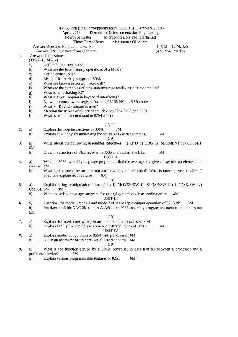
i) Draw the control word register format of 8255 PPI in BSR mode
j) What for RS232 standard is used?
k) Mention the names of all peripheral devices 8254,8259 and 8251
l) What is read back command in 8254 timer?
UNIT I
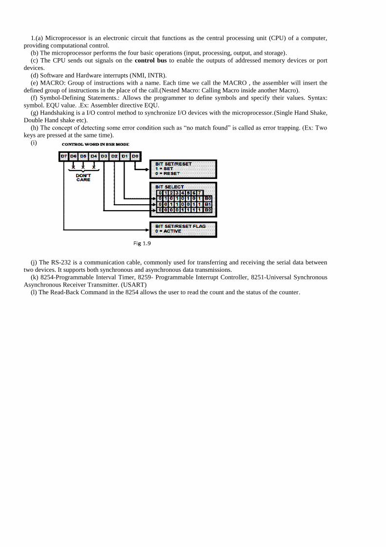
2. a) Explain the loop instructions of 8086? 6M
b) Explain about any six addressing modes in 8086 with examples. 6M
(OR)
3. a) Write about the following assembler directives. i) END ii) ORG iii) SEGMENT iv) OFFSET
6M
b) Draw the structure of Flag register in 8086 and explain the bits. 6M
UNIT II
4. a) Write an 8086 assembly language program to find the average of a given array of data elements of
size ten 4M
b) What do you mean by an interrupt and how they are classified? What is interrupt vector table of
8086 and explain its structure? 8M
(OR)
5. a) Explain string manipulation instructions i) MOVSB/SW ii) STOSB/SW iii) LODSB/SW iv)
CMPSB/SW 8M
b) Write assembly language program for arranging numbers in ascending order 4M
UNIT III
6. a) Describe the mode 0,mode 1 and mode 2 of in the input-output operation of 8255 PPI 6M
b) Interface an 8 bit DAC 08 to port A .Write an 8086 assembly program segment to output a ramp
6M
(OR)
7. a) Explain the interfacing of key board to 8086 microprocessor 6M
b) Explain DAC principle of operation and different types of DACs 6M
UNIT IV
8. a) Explain modes of operation of 8254 with pin diagram 6M
b) Given an overview of RS232C serial data standards 6M
(OR)
9. a) What is the function served by a DMA controller in data transfer between a processor and a
peripheral device? 6M
b) Explain various programmable features of 8251 6M
Page 2
1.(a) Microprocessor is an electronic circuit that functions as the central processing unit (CPU) of a computer,
providing computational control.
(b) The microprocessor performs the four basic operations (input, processing, output, and storage).
(c) The CPU sends out signals on the control bus to enable the outputs of addressed memory devices or port
devices.
(d) Software and Hardware interrupts (NMI, INTR).
(e) MACRO: Group of instructions with a name. Each time we call the MACRO , the assembler will insert the
defined group of instructions in the place of the call.(Nested Macro: Calling Macro inside another Macro).
(f) Symbol-Defining Statements.: Allows the programmer to define symbols and specify their values. Syntax:
symbol. EQU value. .Ex: Assembler directive EQU.
(g) Handshaking is a I/O control method to synchronize I/O devices with the microprocessor.(Single Hand Shake,
Double Hand shake etc).
(h) The concept of detecting some error condition such as “no match found” is called as error trapping. (Ex: Two
keys are pressed at the same time).
(i)
(j) The RS-232 is a communication cable, commonly used for transferring and receiving the serial data between
two devices. It supports both synchronous and asynchronous data transmissions.
(k) 8254-Programmable Interval Timer, 8259- Programmable Interrupt Controller, 8251-Universal Synchronous
Asynchronous Receiver Transmitter. (USART)
(l) The Read-Back Command in the 8254 allows the user to read the count and the status of the counter.
Page 3
2.(a) Loop Instructions f 8086: Explanation of the following instructions.
2(b) 2.Write about addressing modes of 8086 with suitable examples. 12M
ADDRESSING MODES OF 8086:
•Immediate - the data is provided in the instruction.
Ex:MOV AL,34H ;COPY 34H into AL
AL=34H
•Register - references the data in a register or in a register pair.
Ex :MOV AL,BL ;copy the data from BL to AL
Let BL=78H,AL=34H .After executing the instruction BL=34H,AL=34H.
Implied - the data value/data address is implicitly associated with the instruction. Direct - the instruction operand
specifies the memory address where data is located.
Ex :CLC ; CLEAR CARRY FLAG
After executing the instruction CF=0
•Register indirect - instruction specifies a register containing an address, where data is located. This addressing
mode works with SI, DI, BX and BP registers.
•Based :- 8-bit or 16-bit instruction operand is added to the contents of a base register (BX or BP), the resulting
value is a pointer to location where data resides.
Ex :MOV [BP],1223H. ; COPY 1223H into a memory location addressed by DS:BP
Let DS=3000H and BP=4000,then the physical address is 30000+4000=34000H
After executing the instruction the value 1234H is stored in a memory location
whose address is 34000h.
•Indexed :- 8-bit or 16-bit instruction operand is added to the contents of an index register (SI or DI), the
resulting value is a pointer to location where data resides
Ex :MOV [SI],5423H. ; COPY 5423H into a memory location addressed by DS:SI
Let DS=3000H and SI=2000,then the physical address is 30000+2000=32000H
After executing the instruction the value 5423H is stored in a memory location
whose address is 32000h.
•Based Indexed :- the contents of a base register (BX or BP) is added to the contents of an index register (SI or
DI), the resulting value is a pointer to location where data resides.
Ex :MOV [BP][SI],1223H. ; COPY 1223H into a memory location addressed by DS:BP+SI
Let DS=3000H and SI=2000, BP=0100,then the physical address is 30000+2000+0100=32100H
After executing the instruction the value 1223H is stored in a memory location
whose address is 32100h.
Page 4
•Based Indexed with displacement - 8-bit or 16-bit instruction operand is added to the contents of a base
register (BX or BP) and index register (SI or DI), the resulting value is a pointer to location where data resides.
Ex : MOV [BP][SI][09],1223H. ; COPY 1223H into a memory location addressed by DS: BP+SI+09H
Let DS=3000H and SI=2000, BP=0100,then the physical address is 30000+2000+0100+09=32109H
After executing the instruction the value 1223H is stored in a memory location
whose address is 32109h.
3. (a) SEGMENT:
The SEGMENT directive is used to indicate the start of a logical segment. Preceding the SEGMENT directive is
the name you want to give the segment.
For example, the statement CODE SEGMENT indicates to the assembler the start of a logical segment called
CODE. The SEGMENT and ENDS directive are used to “bracket” a logical segment containing code of data.
Additional terms are often added to a SEGMENT directive statement to indicate some special way in which we
want the assembler to treat the segment.
The statement CODE SEGMENT WORD tells the assembler that we want the content of this segment located on
the next available word (even address) when segments ate combined and given absolute addresses.
Without this WORD addition, the segment will be located on the next available paragraph (16-byte) address,
which might waste as much as 15 bytes of memory.
The statement CODE SEGMENT PUBLIC tells the assembler that the segment may be put together with other
segments named CODE from other assembly modules when the modules are linked together.
Example
Name SEGMENT
Variable_name DB …….
Variable_name DW …….
Name ENDS
Data SEGMENT
Data1 DB …….
Data2 DW …….
Data ENDS
Code SEGMENT
START: MOV AX,BX
…
…
…
Code ENDS
ENDS [END SEGMENT ] : This directive is used with the name of a segment to indicate the end of the logical
segment. ENDS is used with the segment directive to ‘bracket’ a logical segment containing instructions or data.
data segment
n1 db 05h
n2 db 04h
sum db ?
data ends
ORG (ORIGIN)
Changes the starting offset address of the data in the data segment. As an assembler assembles a section of a data
declarations or instruction statements, it uses a location counter to keep track of how many bytes it is from the start
of a segment at any time. The location counter is automatically set to 0000 when assembler starts reading a segment.
The ORG directive allows you to set the location counter to a desired value at any point in the program.
Example: The statement ORG 2000H tells the assembler to set the location counter to 2000H.
Page 5
OFFSET
OFFSET is an operator, which tells the assembler to determine the offset or displacement of a named data item
(variable), a procedure from the start of the segment, which contains it.
Example:
MOV BX;
OFFSET PRICES;
It will determine the offset of the variable PRICES from the start of the segment in which PRICES is defined and
will load this value into BX.
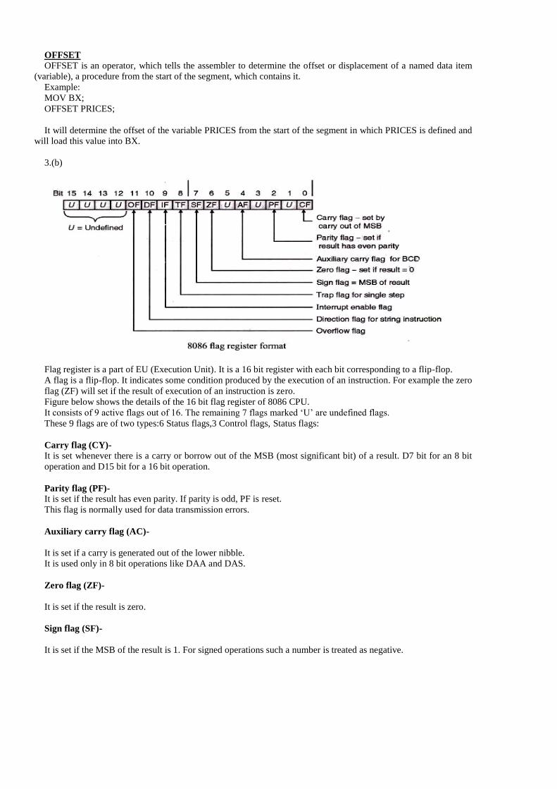
3.(b)
Flag register is a part of EU (Execution Unit). It is a 16 bit register with each bit corresponding to a flip-flop.
A flag is a flip-flop. It indicates some condition produced by the execution of an instruction. For example the zero
flag (ZF) will set if the result of execution of an instruction is zero.
Figure below shows the details of the 16 bit flag register of 8086 CPU.
It consists of 9 active flags out of 16. The remaining 7 flags marked ‘U’ are undefined flags.
These 9 flags are of two types:6 Status flags,3 Control flags, Status flags:
Carry flag (CY)-
It is set whenever there is a carry or borrow out of the MSB (most significant bit) of a result. D7 bit for an 8 bit
operation and D15 bit for a 16 bit operation.
Parity flag (PF)-
It is set if the result has even parity. If parity is odd, PF is reset.
This flag is normally used for data transmission errors.
Auxiliary carry flag (AC)-
It is set if a carry is generated out of the lower nibble.
It is used only in 8 bit operations like DAA and DAS.
Zero flag (ZF)-
It is set if the result is zero.
Sign flag (SF)-
It is set if the MSB of the result is 1. For signed operations such a number is treated as negative.
Page 6
Overflow flag (OF)- It will be set if the result of a signed operation is too large to fit in the number of bits available to represent it.
It can be checked using the instruction INTO (Interrupt on Overflow).
Control flags:
Trap flag (TF)-
It is used to set the trace mode i.e. start single stepping mode.
Here the microprocessor is interrupted after every instruction so that the program can be debugged.
Interrupt enable flag (IF)-
It is used to mask (disable) or unmask (enable) the INTR interrupt.
If user sets IF flag, the CPU will recognize external interrupt requests. Clearing IF disables these interrupts.
Direction flag (DF)-
If this flag is set, SI and DI are in auto-decrementing mode in string operations.
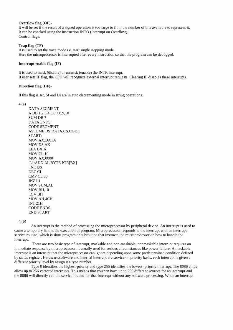
4.(a)
DATA SEGMENT
A DB 1,2,3,4,5,6,7,8,9,10
SUM DB ?
DATA ENDS
CODE SEGMENT
ASSUME DS:DATA,CS:CODE
START:
MOV AX,DATA
MOV DS,AX
LEA BX,A
MOV CL,10
MOV AX,0000
L1:ADD AL,BYTE PTR[BX]
INC BX
DEC CL
CMP CL,00
JNZ L1
MOV SUM,AL
MOV BH,10
DIV BH
MOV AH,4CH
INT 21H
CODE ENDS
END START
4.(b)
An interrupt is the method of processing the microprocessor by peripheral device. An interrupt is used to
cause a temporary halt in the execution of program. Microprocessor responds to the interrupt with an interrupt
service routine, which is short program or subroutine that instructs the microprocessor on how to handle the
interrupt.
There are two basic type of interrupt, maskable and non-maskable, nonmaskable interrupt requires an
immediate response by microprocessor, it usually used for serious circumstances like power failure. A maskable
interrupt is an interrupt that the microprocessor can ignore depending upon some predetermined condition defined
by status register. Hardware,software and internal interrupt are service on priority basis. each interrupt is given a
different priority level by assign it a type number.
Type 0 identifies the highest-priority and type 255 identifies the lowest- priority interrupt. The 8086 chips
allow up to 256 vectored interrupts. This means that you can have up to 256 different sources for an interrupt and
the 8086 will directly call the service routine for that interrupt without any software processing. When an interrupt
Page 7
occurs regardless of source, the 8086 does the following: 1. The CPU pushes the flags register onto the
stack. 2. The CPU pushes a far return address (segment:offset) onto the stack, segment value first. 3. The CPU
determines the cause of the interrupt (i.e., the interrupt number) and fetches the four byte interrupt vector from
address 0:vector*4. 4. The CPU transfers control to the routine specified by the interrupt vector table entry. When
the interrupt service routine wants to return control, it must execute an IRET (interrupt return) instruction. The
interrupt return pops the far return address and the flags off the stack. Note that executing a far return is insufficient
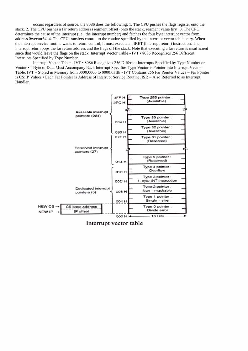
since that would leave the flags on the stack. Interrupt Vector Table - IVT • 8086 Recognizes 256 Different
Interrupts Specified by Type Number.
Interrupt Vector Table - IVT • 8086 Recognizes 256 Different Interrupts Specified by Type Number or
Vector • 1 Byte of Data Must Accompany Each Interrupt Specifies Type Vector is Pointer into Interrupt Vector
Table, IVT – Stored in Memory from 0000:0000 to 0000:03ffh • IVT Contains 256 Far Pointer Values – Far Pointer
is CS:IP Values • Each Far Pointer is Address of Interrupt Service Routine, ISR – Also Referred to as Interrupt
Handler.
Page 8
5.(a)
A series of data byte or word available in memory at consecutive locations, to be referred as Byte String or Word
String. A String of characters may be located in consecutive memory locations, where each character may be
represented by its ASCII equivalent.
The 8086 supports a set of more powerful instructions for string manipulations for referring to a string, two
parameters are required.
I. Starting and End Address of the String.
II. Length of the String.
The length of the string is usually stored as count in the CX register.The incrementing or decrementing of the
pointer, in string instructions, depends upon the Direction Flag (DF) Status. If it is a Byte string operation, the index
registers are updated by one. On the other hand, if it is a word string operation, the index registers are updated by
two.
MOVSB / MOVSW :Move String Byte or String Word
Suppose a string of bytes stored in a set of consecutive memory locations is to be moved to another set of destination
locations.The starting byte of source string is located in the memory location whose address may be computed using
SI (Source Index) and DS (Data Segment) contents. The starting address of the destination locations where this
string has to be relocated is given by DI (Destination Index) and ES (Extra Segment) contents.
CMPS : Compare String Byte or String Word
The CMPS instruction can be used to compare two strings of byte or words. The length of the string must be stored
in the register CX. If both the byte or word strings are equal, zero Flag is set.The REP instruction Prefix is used to
repeat the operation till CX (counter) becomes zero or the condition specified by the REP Prefix is False.
LODS : Load String Byte or String Word
The LODS instruction loads the AL / AX register by the content of a string pointed to by DS : SI register pair. The
SI is modified automatically depending upon DF, If it is a byte transfer (LODSB), the SI is modified by one and if it
is a word transfer (LODSW), the SI is modified by two. No other Flags are affected by this instruction.
STOS : Store String Byte or String Word
The STOS instruction Stores the AL / AX register contents to a location in the string pointer by ES : DI register pair.
The DI is modified accordingly, No Flags are affected by this instruction. The direction Flag controls the String
instruction execution, The source index SI and Destination Index DI are modified after each iteration automatically.
If DF=1, then the execution follows autodecrement mode, SI and DI are decremented automatically after each
iteration. If DF=0, then the execution follows autoincrement mode. In this mode, SI and DI are incremented
automatically after each iteration.
5.(b)
ASSUME CS:CODE,DS:DATA
DATA SEGMENT
ORG 2000H
SERIES DB 81H,82H,93H,95H,10H,56H,33H,99H,13H,44H
COUNT DW 10D
DATA ENDS
CODE SEGMENT
START:MOV AX,DATA
MOV DS,AX
Page 9
MOV DX,COUNT
DEC DX
GO:MOV CX,DX
LEA SI,SERIES
NXT_BYTE:MOV AL,[SI]
CMP AL,[SI+1]
JB NEXT
XCHG AL,[SI+1]
XCHG AL,[SI]
NEXT:INC SI
LOOP NXT_BYTE
DEC DX
JNZ GO
MOV AH,4CH
INT 21H
CODE ENDS
END START
6.(a)
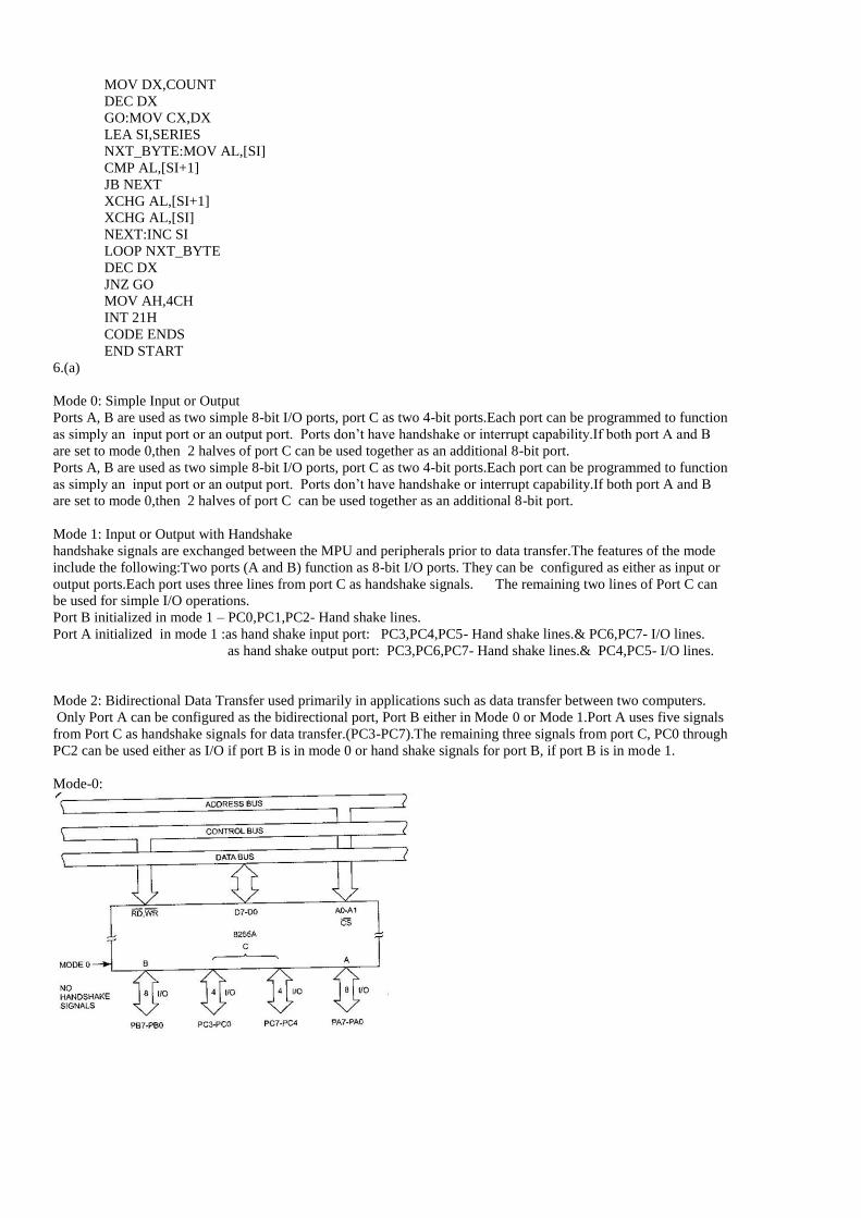
Mode 0: Simple Input or Output
Ports A, B are used as two simple 8-bit I/O ports, port C as two 4-bit ports.Each port can be programmed to function
as simply an input port or an output port. Ports don’t have handshake or interrupt capability.If both port A and B
are set to mode 0,then 2 halves of port C can be used together as an additional 8-bit port.
Mode 1: Input or Output with Handshake
handshake signals are exchanged between the MPU and peripherals prior to data transfer.The features of the mode
include the following:Two ports (A and B) function as 8-bit I/O ports. They can be configured as either as input or
output ports.Each port uses three lines from port C as handshake signals. The remaining two lines of Port C can
be used for simple I/O operations.
Port B initialized in mode 1 – PC0,PC1,PC2- Hand shake lines.
Port A initialized in mode 1 :as hand shake input port: PC3,PC4,PC5- Hand shake lines.& PC6,PC7- I/O lines.
as hand shake output port: PC3,PC6,PC7- Hand shake lines.& PC4,PC5- I/O lines.
Mode 2: Bidirectional Data Transfer used primarily in applications such as data transfer between two computers.
Only Port A can be configured as the bidirectional port, Port B either in Mode 0 or Mode 1.Port A uses five signals
from Port C as handshake signals for data transfer.(PC3-PC7).The remaining three signals from port C, PC0 through
PC2 can be used either as I/O if port B is in mode 0 or hand shake signals for port B, if port B is in mode 1.
Mode-0:
Page 10
Mode-1:
Mode-2:
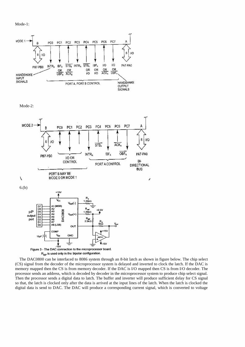
6.(b)
The DAC0800 can be interfaced to 8086 system through an 8-bit latch as shown in figure below. The chip select
(CS) signal from the decoder of the microprocessor system is delayed and inverted to clock the latch. If the DAC is
memory mapped then the CS is from memory decoder. If the DAC is I/O mapped then CS is from I/O decoder. The
processor sends an address, which is decoded by decoder in the microprocessor system to produce chip select signal.
Then the processor sends a digital data to latch. The buffer and inverter will produce sufficient delay for CS signal
so that, the latch is clocked only after the data is arrived at the input lines of the latch. When the latch is clocked the
digital data is send to DAC. The DAC will produce a corresponding current signal, which is converted to voltage
Page 11
7.(a)
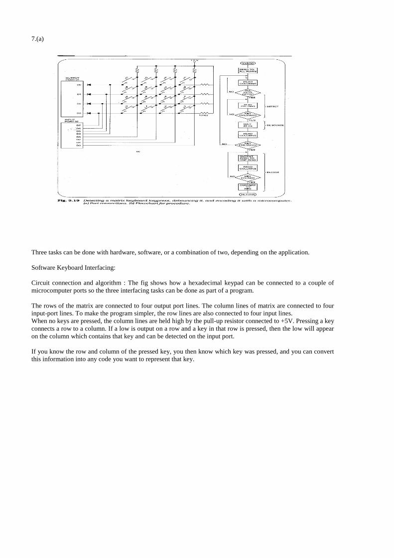
Three tasks can be done with hardware, software, or a combination of two, depending on the application.
Software Keyboard Interfacing:
Circuit connection and algorithm : The fig shows how a hexadecimal keypad can be connected to a couple of
microcomputer ports so the three interfacing tasks can be done as part of a program.
The rows of the matrix are connected to four output port lines. The column lines of matrix are connected to four
input-port lines. To make the program simpler, the row lines are also connected to four input lines.
When no keys are pressed, the column lines are held high by the pull-up resistor connected to +5V. Pressing a key
connects a row to a column. If a low is output on a row and a key in that row is pressed, then the low will appear
on the column which contains that key and can be detected on the input port.
If you know the row and column of the pressed key, you then know which key was pressed, and you can convert
this information into any code you want to represent that key.
Page 12
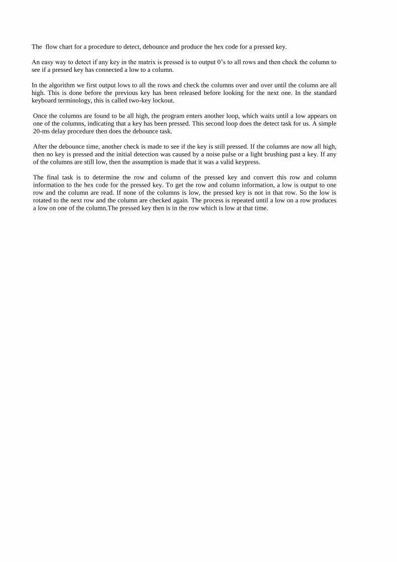
The flow chart for a procedure to detect, debounce and produce the hex code for a pressed key.
An easy way to detect if any key in the matrix is pressed is to output 0’s to all rows and then check the column to
see if a pressed key has connected a low to a column.
In the algorithm we first output lows to all the rows and check the columns over and over until the column are all
high. This is done before the previous key has been released before looking for the next one. In the standard
keyboard terminology, this is called two-key lockout.
Once the columns are found to be all high, the program enters another loop, which waits until a low appears on
one of the columns, indicating that a key has been pressed. This second loop does the detect task for us. A simple
20-ms delay procedure then does the debounce task.
After the debounce time, another check is made to see if the key is still pressed. If the columns are now all high,
then no key is pressed and the initial detection was caused by a noise pulse or a light brushing past a key. If any
of the columns are still low, then the assumption is made that it was a valid keypress.
The final task is to determine the row and column of the pressed key and convert this row and column
information to the hex code for the pressed key. To get the row and column information, a low is output to one
row and the column are read. If none of the columns is low, the pressed key is not in that row. So the low is
rotated to the next row and the column are checked again. The process is repeated until a low on a row produces
a low on one of the column.The pressed key then is in the row which is low at that time.
Page 13
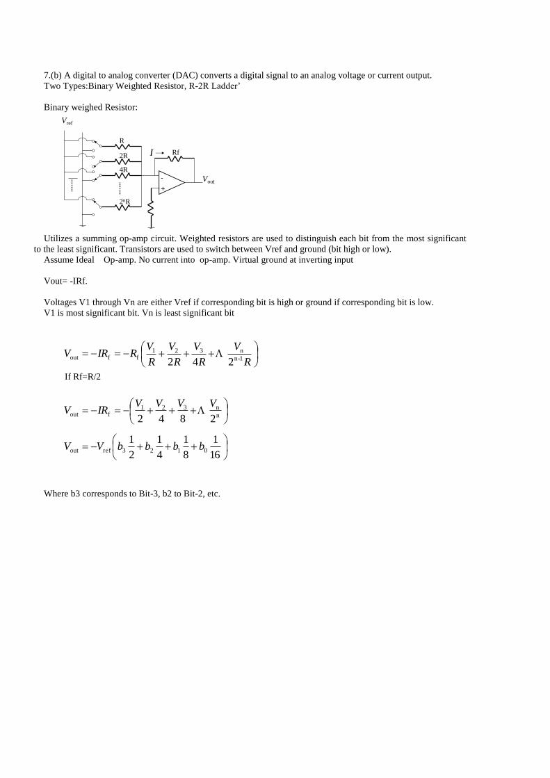
7.(b) A digital to analog converter (DAC) converts a digital signal to an analog voltage or current output.
Two Types:Binary Weighted Resistor, R-2R Ladder’
Binary weighed Resistor:
Utilizes a summing op-amp circuit. Weighted resistors are used to distinguish each bit from the most significant
to the least significant. Transistors are used to switch between Vref and ground (bit high or low).
Assume Ideal Op-amp. No current into op-amp. Virtual ground at inverting input
Vout= -IRf.
Voltages V1 through Vn are either Vref if corresponding bit is high or ground if corresponding bit is low.
V1 is most significant bit. Vn is least significant bit
If Rf=R/2
Where b3 corresponds to Bit-3, b2 to Bit-2, etc.
-
+
R
2R
4R
2nR
Rf
Vout
I
Vref
R
V
R
V
R
V
R
VRIRV
1-n
n321ffout
242
n
n321fout
2842
VVVVIRV
16
1
8
1
4
1
2
10123refout bbbbVV
Page 14
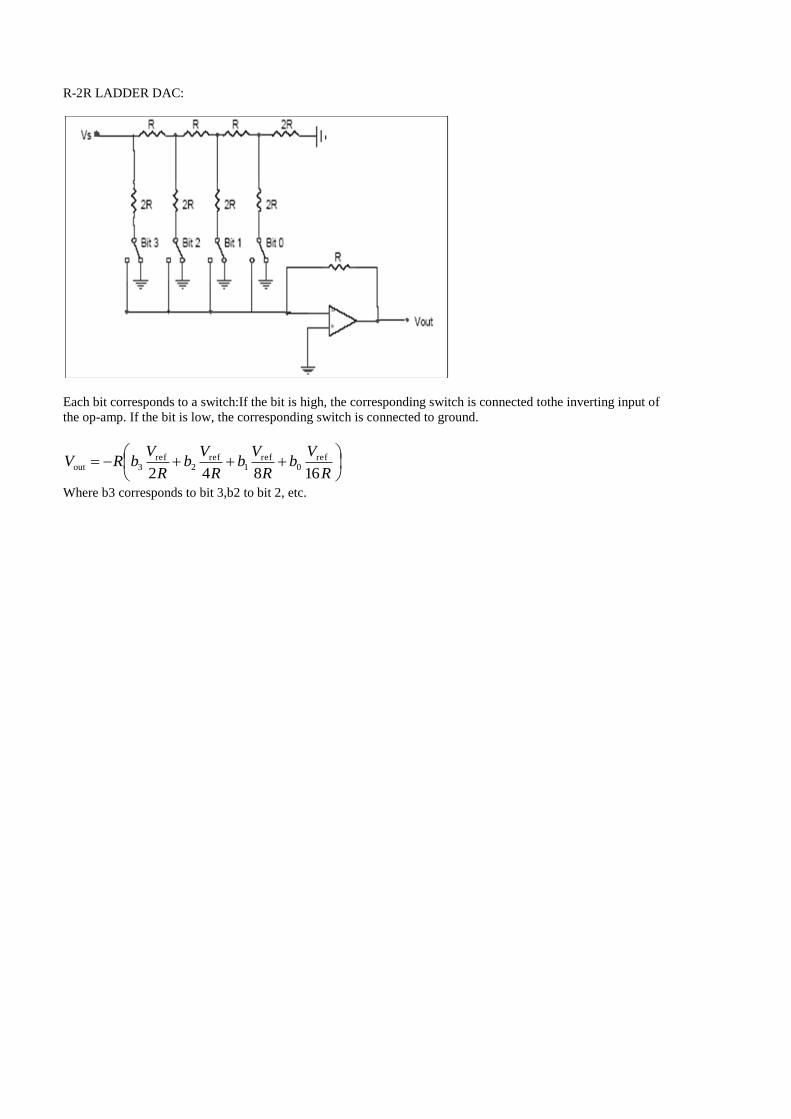
R-2R LADDER DAC:
Each bit corresponds to a switch:If the bit is high, the corresponding switch is connected tothe inverting input of
the op-amp. If the bit is low, the corresponding switch is connected to ground.
R
Vb
R
Vb
R
Vb
R
VbRV
16842
ref0
ref1
ref2
ref3out
Where b3 corresponds to bit 3,b2 to bit 2, etc.
Page 15
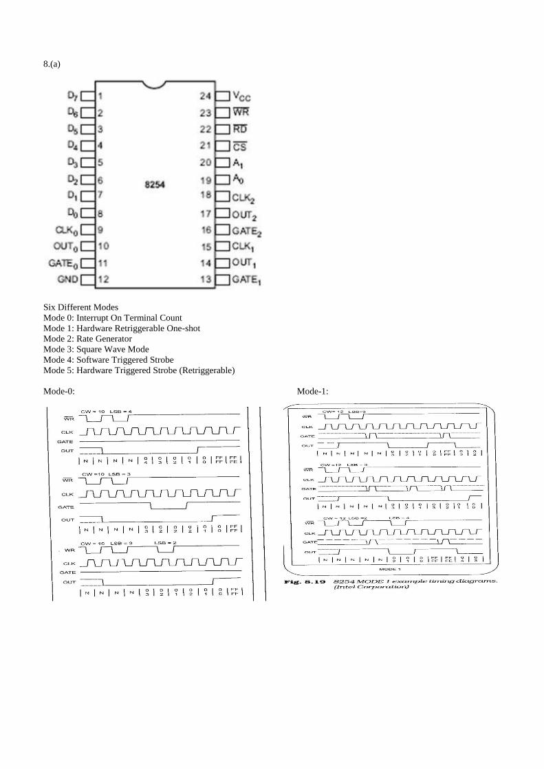
8.(a)
Six Different Modes
Mode 0: Interrupt On Terminal Count
Mode 1: Hardware Retriggerable One-shot
Mode 2: Rate Generator
Mode 3: Square Wave Mode
Mode 4: Software Triggered Strobe
Mode 5: Hardware Triggered Strobe (Retriggerable)
Mode-0: Mode-1:
Page 16
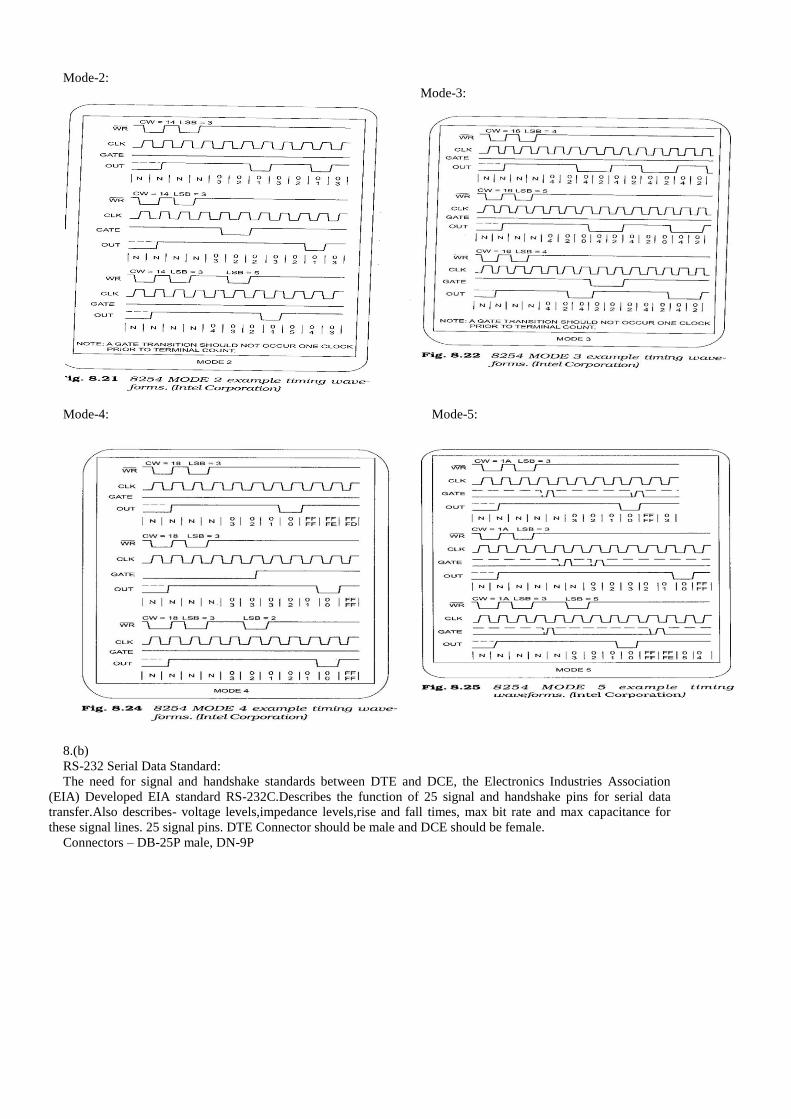
Mode-2:
Mode-3:
Mode-4: Mode-5:
8.(b)
RS-232 Serial Data Standard:
The need for signal and handshake standards between DTE and DCE, the Electronics Industries Association
(EIA) Developed EIA standard RS-232C.Describes the function of 25 signal and handshake pins for serial data
transfer.Also describes- voltage levels,impedance levels,rise and fall times, max bit rate and max capacitance for
these signal lines. 25 signal pins. DTE Connector should be male and DCE should be female.
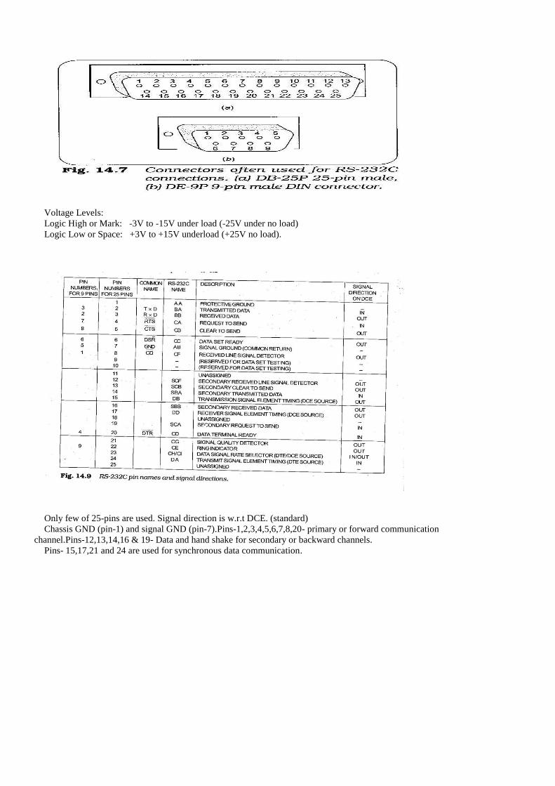
Connectors – DB-25P male, DN-9P
Page 17
Voltage Levels:
Logic High or Mark: -3V to -15V under load (-25V under no load)
Logic Low or Space: +3V to +15V underload (+25V no load).
Only few of 25-pins are used. Signal direction is w.r.t DCE. (standard)
Chassis GND (pin-1) and signal GND (pin-7).Pins-1,2,3,4,5,6,7,8,20- primary or forward communication
channel.Pins-12,13,14,16 & 19- Data and hand shake for secondary or backward channels.
Pins- 15,17,21 and 24 are used for synchronous data communication.
Page 18
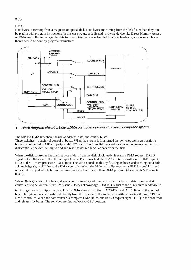
9.(a).
DMA:
Data bytes to memory from a magnetic or optical disk. Data bytes are coming from the disk faster than they can
be read in with program instructions. In this case we use a dedicated hardware device like Direct Memory Access
or DMA controller to manage the data transfer. Data transfer is handled totally in hardware, so it is much faster
than it would be done by program instructions.
The MP and DMA timeshare the use of address, data, and control buses.
Three switches – transfer of control of buses. When the system is first turned on- switches are in up position (
buses are connected to MP and peripherals). TO read a file from disk we send a series of commands to the smart
disk controller device , telling to find and read the desired block of data from the disk.
When the disk controller has the first byte of data from the disk block ready, it sends a DMA request, DREQ
signal to the DMA controller. If that input (channel) is unmasked, the DMA controller will send HOLD request,
HRQ to the microprocessor HOLD input.The MP responds to this by floating its buses and sending out a hold-
acknowledge signal, HLDA to the DMA controller.When the DMA controller receives a HLDA signal it’ll send
out a control signal which throws the three bus switches down to their DMA position. (disconnects MP from its
buses).
When DMA gets control of buses, it sends put the memory address where the first byte of data from the disk
controller is to be written. Next DMA sends DMA-acknowledge , DACKO, signal to the disk controller device to
tell it to get ready to output the byte. Finally DMA asserts both the MEMW and IOR lines on the control
bus. The byte of data is transferred directly from the disk controller to memory without passing through CPU and
DMA controller. When the data transfer is complete DMA un-asserts HOLD request signal, HRQ to the processor
and releases the buses. The switches are thrown back to CPU position.
Page 19
9.(b).
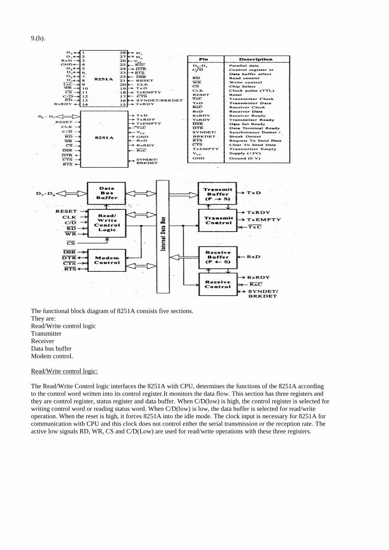
The functional block diagram of 8251A consists five sections.
They are:
Read/Write control logic
Transmitter
Receiver
Data bus buffer
Modem control.
Read/Write control logic:
The Read/Write Control logic interfaces the 8251A with CPU, determines the functions of the 8251A according
to the control word written into its control register.It monitors the data flow. This section has three registers and
they are control register, status register and data buffer. When C/D(low) is high, the control register is selected for
writing control word or reading status word. When C/D(low) is low, the data buffer is selected for read/write
operation. When the reset is high, it forces 8251A into the idle mode. The clock input is necessary for 8251A for
communication with CPU and this clock does not control either the serial transmission or the reception rate. The
active low signals RD, WR, CS and C/D(Low) are used for read/write operations with these three registers.
Page 20
Transmitter:
The transmitter section accepts parallel data from CPU and converts them into serial data.
The transmitter section is double buffered, i.e., it has a buffer register to hold an 8-bit parallel data and another
register called output register to convert the parallel data into serial bits.
When output register is empty, the data is transferred from buffer to output register. Now the processor can again
load another data in buffer register. If buffer register is empty, then TxRDY is goes to high.
If output register is empty then TxEMPTY goes to high. The clock signal, TxC (low) controls the rate at which
the bits are transmitted by the USART. The clock frequency can be 1,16 or 64 times the baud rate.
Receiver:
The receiver section accepts serial data and convert them into parallel data.The receiver section is double
buffered, i.e., it has an input register to receive serial data and convert to parallel, and a buffer register to hold the
parallel data.When the RxD line goes low, the control logic assumes it as a START bit, waits for half a bit time
and samples the line again.If the line is still low, then the input register accepts the following bits, forms a
character and loads it into the buffer register.
The CPU reads the parallel data from the buffer register. When the input register loads a parallel data to buffer
register, the RxRDY line goes high.The clock signal RxC (low) controls the rate at which bits are received by the
USART. During asynchronous mode, the signal SYNDET/BRKDET will indicate the break in the data
transmission. During synchronous mode, the signal SYNDET/BRKDET will indicate the reception of
synchronous character.
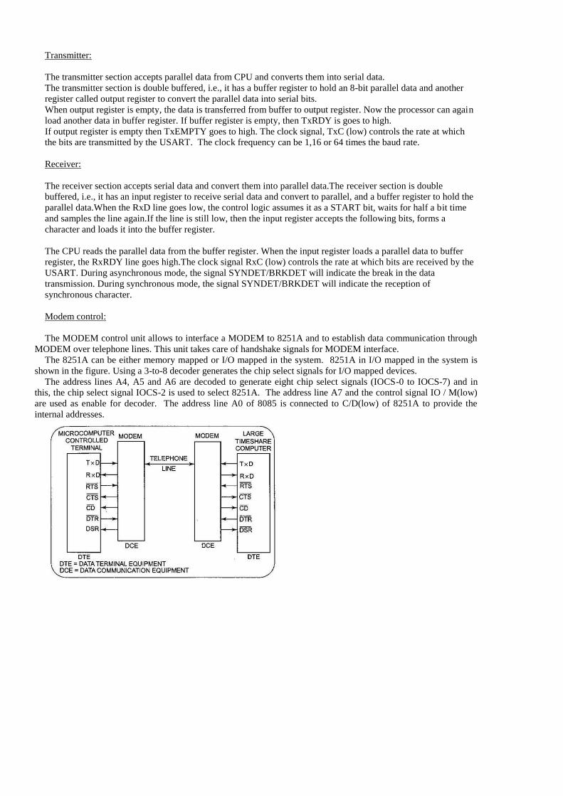
Modem control:
The MODEM control unit allows to interface a MODEM to 8251A and to establish data communication through
MODEM over telephone lines. This unit takes care of handshake signals for MODEM interface.
The 8251A can be either memory mapped or I/O mapped in the system. 8251A in I/O mapped in the system is
shown in the figure. Using a 3-to-8 decoder generates the chip select signals for I/O mapped devices.
The address lines A4, A5 and A6 are decoded to generate eight chip select signals (IOCS-0 to IOCS-7) and in
this, the chip select signal IOCS-2 is used to select 8251A. The address line A7 and the control signal IO / M(low)
are used as enable for decoder. The address line A0 of 8085 is connected to C/D(low) of 8251A to provide the
internal addresses.