IJECT VOL. 8, ISSUE 2, APRIL - JUNE 2017 www.iject.org INTERNATIONAL JOURNAL OF ELECTRONICS & COMMUNICATION TECHNOLOGY 9 ISSN : 2230-7109 (Online) | ISSN : 2230-9543 (Print) FPGA Implementation of LTE-Advanced Downlink Physical Layer Transceiver 1 Sara M. Hassan, 2 Abdelhalim Zekry 1 Modern Academy, Cairo, Egypt 2 Ain Shams University, Cairo, Egypt Abstract To achieve a higher bit rates up to 1 Gbps for meeting the growing needs of the users of the mobile communication system the 3rd Generation Partnership Project (3GPP) introduced the Long Term Evolution Advanced (LTE-A) as an advanced standard for the mobile communication systems. The new features added by the LTE-A on the physical layer is a direct consequence for applying new modulation and coding techniques for both the Uplink and Downlink. The Orthogonal Frequency Division Multiple Access (OFDMA) was applied for the Downlink and the Single Carrier Frequency Division Multiple Access (SC-FDMA) was applied for the Uplink as well as turbo coding. This paper presents the design and implementation of the LTE-A downlink transmitter and receiver using a Field Programmable Gate Array (FPGA) according to release 10/11 on Virtex 6 XC6VLX240T FPGA kit using Xilinx® ISE® Design Suite version 13.3.All stages of the LTE-A downlink physical layer (PYH) transceiver, besides the time and frequency synchronization in a receiver,are implemented with 2x2 MIMO and Intra-band contiguous Carrier Aggregation type with two Component Carriers. Keywords LTE, 4G, 3GPP, OFDM, LTE-advanced downlink physical layer, release 10, release 11,Xilinx Design Suite, virtex 6 XC6VLX240T FPGA. I. Introduction The 3GPP has introduced the complete specifications of LTE-A to meet the growing needs to higher data rates in mobile communication systems. LTE Release 8 can provide up to 50 Mbps for uplink and 100 Mbps for downlink, while LTE-A, starting from Release 10, can provide up to 1 Gbps as peak data rates for downlink, as well as higher throughput, higher coverage, and lower latencies [1-9]. LTE and LTE-A have a scalable bandwidth of 1.4, 3, 5, 10, 15 or 20 MHz. The LTE-A PHY is a highly efficient facility for conveying both data and control information between an enhanced base station (eNodeB) and mobile User Equipment (UE). OFDMA is utilized in LTE-A downlink PHY while SC-FDMA is used in the uplink [10]. For higher data rates, the LTE-A should support Carrier Aggregation (CA) that act as a solution to bandwidth extension for large transmission bandwidths from 40 MHz to 100MHz and high peak data rate of 500 Mbps in the uplink and 1Gbps in the downlink [11-14]. There are three Carrier Aggregation scenarios; which are Intra-band contiguous, Intra-band non-contiguous and Inter-band non-contiguous Carrier Aggregation. The Intra-band contiguous uses a single frequency band and is the simplest form of CA from the implementation point of view while the Intra-band non-contiguous is aggregate, not adjacent multi-carriers, then two transceivers may be required. This adds a significant complexity to the UE, an increase the amount of power consumption and an increase in the cost. The Inter-band non-contiguous type uses different frequency bands. That is why the UE may have to use multiple transceivers. So, the cost, performance and power consumption are affected considerably. On the other side it can improve the system mobility by exploiting the radio propagation characteristics of different bands [15-18]. Also, LTE-A supports the Multipoint Transmission and Reception as Multi Input Multi Output (MIMO) that ensure more system throughput. The MIMO systems can achieve significant higher data rates more than the traditional single-input, single- output (SISO) channels [19-20]. This paper presents the design and implementation of the LTE-A downlink PYH transceiver. The design is based on 2x2 MIMO and Intra-band contiguous CA type with two Component Carriers (CCs). The implementation is done using FPGA on Virtex 6 XC6VLX240T FPGA kit according to release 10 using Xilinx package version 13.3. The implementation of every stage in both the transmitter and receiver is verified. The paper is organized such that: section two presents the design and implementation of the LTE-A transmitter and receiver building blocks. Section III introduces the full system verification while the full system and its area optimization strategy utilization on the Xilinx Vertix 6 are described in section four and the carrier aggregation scenario in section five. II. LTE-Advanced Transimitter and Reciver Implemen- tation The implementation of LTE-advanced in this paper is built according to release 10 specifications with Frequency Division Duplex (FDD) frame structure. The bandwidth of the implemented system is 3 MHz, the number of sub-channels is 15, the number of sub-carrier is 180, the Inverse Fast Fourier Transform (IFFT) and the Fast Fourier Transform (FFT) size are 256, the rate of turbo encoder/decoder is 1/3, and the system input data is one OFDM symbol with length 96 bits [21]. The implemented transmitter and receiver block diagrams are shown in Figure 1 and Figure 2 respectively. In the following sections, all the building blocks in the transmitter are implemented with the FPGA and their reverse operations are done in the receiver. Finally, the overall system verification (transmitter/receiver) was done. Fig. 1: The Block Diagram of the LTE-Advanced Downlink Physical Layer Transmitter [21]. Fig. 2: The Block Diagram of the LTE- Advanced Downlink Physical Layer Receiver [21].
Transcript
IJECT Vol. 8, IssuE 2, AprIl - JunE 2017
w w w . i j e c t . o r g InternatIonal Journal of electronIcs & communIcatIon technology 9
FPGA Implementation of LTE-Advanced Downlink Physical Layer Transceiver
1Sara M. Hassan, 2Abdelhalim Zekry1Modern Academy, Cairo, Egypt
2Ain Shams University, Cairo, Egypt
AbstractTo achieve a higher bit rates up to 1 Gbps for meeting the growing needs of the users of the mobile communication system the 3rd Generation Partnership Project (3GPP) introduced the Long Term Evolution Advanced (LTE-A) as an advanced standard for the mobile communication systems. The new features added by the LTE-A on the physical layer is a direct consequence for applying new modulation and coding techniques for both the Uplink and Downlink. The Orthogonal Frequency Division Multiple Access (OFDMA) was applied for the Downlink and the Single Carrier Frequency Division Multiple Access (SC-FDMA) was applied for the Uplink as well as turbo coding. This paper presents the design and implementation of the LTE-A downlink transmitter and receiver using a Field Programmable Gate Array (FPGA) according to release 10/11 on Virtex 6 XC6VLX240T FPGA kit using Xilinx® ISE® Design Suite version 13.3.All stages of the LTE-A downlink physical layer (PYH) transceiver, besides the time and frequency synchronization in a receiver,are implemented with 2x2 MIMO and Intra-band contiguous Carrier Aggregation type with two Component Carriers.
I. IntroductionThe 3GPP has introduced the complete specifications of LTE-A to meet the growing needs to higher data rates in mobile communication systems. LTE Release 8 can provide up to 50 Mbps for uplink and 100 Mbps for downlink, while LTE-A, starting from Release 10, can provide up to 1 Gbps as peak data rates for downlink, as well as higher throughput, higher coverage, and lower latencies [1-9].LTE and LTE-A have a scalable bandwidth of 1.4, 3, 5, 10, 15 or 20 MHz. The LTE-A PHY is a highly efficient facility for conveying both data and control information between an enhanced base station (eNodeB) and mobile User Equipment (UE). OFDMA is utilized in LTE-A downlink PHY while SC-FDMA is used in the uplink [10].For higher data rates, the LTE-A should support Carrier Aggregation (CA) that act as a solution to bandwidth extension for large transmission bandwidths from 40 MHz to 100MHz and high peak data rate of 500 Mbps in the uplink and 1Gbps in the downlink [11-14]. There are three Carrier Aggregation scenarios; which are Intra-band contiguous, Intra-band non-contiguous and Inter-band non-contiguous Carrier Aggregation. The Intra-band contiguous uses a single frequency band and is the simplest form of CA from the implementation point of view while the Intra-band non-contiguous is aggregate, not adjacent multi-carriers, then two transceivers may be required. This adds a significant complexity to the UE, an increase the amount of power consumption and an increase in the cost. The Inter-band non-contiguous type uses different frequency bands. That is why the UE may have to use multiple transceivers. So, the cost, performance and power consumption are affected
considerably. On the other side it can improve the system mobility by exploiting the radio propagation characteristics of different bands [15-18]. Also, LTE-A supports the Multipoint Transmission and Reception as Multi Input Multi Output (MIMO) that ensure more system throughput. The MIMO systems can achieve significant higher data rates more than the traditional single-input, single-output (SISO) channels [19-20]. This paper presents the design and implementation of the LTE-A downlink PYH transceiver. The design is based on 2x2 MIMO and Intra-band contiguous CA type with two Component Carriers (CCs). The implementation is done using FPGA on Virtex 6 XC6VLX240T FPGA kit according to release 10 using Xilinx package version 13.3. The implementation of every stage in both the transmitter and receiver is verified. The paper is organized such that: section two presents the design and implementation of the LTE-A transmitter and receiver building blocks. Section III introduces the full system verification while the full system and its area optimization strategy utilization on the Xilinx Vertix 6 are described in section four and the carrier aggregation scenario in section five.
II. LTE-Advanced Transimitter and Reciver Implemen-tationThe implementation of LTE-advanced in this paper is built according to release 10 specifications with Frequency Division Duplex (FDD) frame structure. The bandwidth of the implemented system is 3 MHz, the number of sub-channels is 15, the number of sub-carrier is 180, the Inverse Fast Fourier Transform (IFFT) and the Fast Fourier Transform (FFT) size are 256, the rate of turbo encoder/decoder is 1/3, and the system input data is one OFDM symbol with length 96 bits [21]. The implemented transmitter and receiver block diagrams are shown in Figure 1 and Figure 2 respectively. In the following sections, all the building blocks in the transmitter are implemented with the FPGA and their reverse operations are done in the receiver. Finally, the overall system verification (transmitter/receiver) was done.
Fig. 1: The Block Diagram of the LTE-Advanced Downlink Physical Layer Transmitter [21].
Fig. 2: The Block Diagram of the LTE- Advanced Downlink Physical Layer Receiver [21].
IJECT Vol. 8, IssuE 2, AprIl - JunE 2017 Issn : 2230-7109 (online) | Issn : 2230-9543 (Print)
w w w . i j e c t . o r g 10 InternatIonal Journal of electronIcs & communIcatIon technology
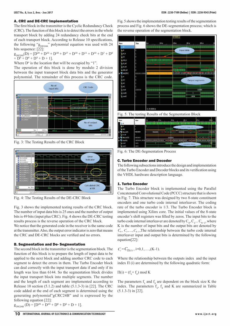
A. CRC and DE-CRC ImplementationThe first block in the transmitter is the Cyclic Redundancy Check (CRC). The function of this block is to detect the errors in the whole transport block by adding 24 redundancy check bits at the end of each transport block. According to Release 10 specifications, the following “gCRC24A” polynomial equation was used with 24 bits sequence: [22]:gCRC24A(D) = [D24 + D23 + D18 + D17 + D14 + D11 + D10 + D7 + D6 + D5 + D4 + D3 + D + 1].Where Dn is the location that will be occupied by “1”. The operation of this block is done by modulo 2 division between the input transport block data bits and the generator polynomial. The remainder of this process is the CRC code.
Fig. 3: The Testing Results of the CRC Block
Fig. 4: The Testing Results of the DE-CRC Block
Fig. 3 shows the implemented testing results of the CRC block. The number of input data bits is 25 ones and the number of output bits is 49 bits (input plus CRC). Fig. 4 shows the DE-CRC testing results process is the reverse operation of the CRC block.We notice that the generated code in the receiver is the same code at the transmitter. Also, the output error indicator is zero that means the CRC and DE-CRC blocks are verified and no errors.
B. Segmentation and De- SegmentationThe second block in the transmitter is the segmentation block. The function of this block is to prepare the length of input data to be applied to the next block and adding another CRC code to each segment to detect the errors in them. The Turbo Encoder block can deal correctly with the input transport data if and only if its length was less than 6144. So the segmentation block divides the input transport block into multiple segments. The number and the length of each segment are implemented according to Release 10 section (5.1.2) and table (5.1.3-3) in [22]. The CRC code added at the end of each segment is determined using the generating polynomial”gCRC24B” and is expressed by the following equation [22]:gCRC24B (D) = [D24 + D23 + D6 + D5 + D + 1].
Fig. 5 shows the implementation testing results of the segmentation process and Fig. 6 shows the DE-segmentation process; which is the reverse operation of the segmentation block.
Fig. 5: The testing Results of the Segmentation Block
Fig. 6: The DE-Segmentation Process
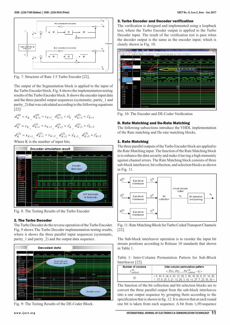
C. Turbo Encoder and DecoderThe following subsections introduce the design and implementation of the Turbo Encoder and Decoder blocks and its verification using the VHDL hardware description language.
1. Turbo EncoderThe Turbo Encoder block is implemented using the Parallel Concatenated Convolutional Code (PCCC) structure that is shown in Fig. 7. This structure was designed by two 8-state constituent encoders and one turbo code internal interleaver. The coding rate of the turbo encoder is 1/3. The Turbo Encoder block is implemented using Xilinx core. The initial values of the 8-state encoder’s shift registers was filled by zeros. The input bits to the turbo code internal interleaver are denoted by C0, C1... CK−1, where K is the number of input bits and the output bits are denoted by
'0C , '
1C ,…, '1−KC ,The relationship between the turbo code internal
interleaver input and output bits is determined by the following equation[22]:
'iC = )(iC∏ , i=0,1,….,(K-1).
Where the relationship between the outputs index and the input index Π (i) are determined by the following quadratic form:
Π(i) = (f1+ f2) mod K
The parameters f1 and f2 are dependent on the block size K the index. The parameters f1, f2 and K are summarized in Table (5.1.3-3) in [22].
IJECT Vol. 8, IssuE 2, AprIl - JunE 2017
w w w . i j e c t . o r g InternatIonal Journal of electronIcs & communIcatIon technology 11
The output of the Segmentation block is applied to the input of the Turbo Encoder block. Fig. 8 shows the implementation testing results of the Turbo Encoder block. It shows the encoder input data and the three parallel output sequences (systematic, parity_1 and parity_2) that was calculated according to the following equations [22]:
KK xd =)0(, 1
)0(1 ++ = KK zd , KK xd ′=+
)0(2 , 1
)0(3 ++ ′= KK zd
KK zd =)1(, 2
)1(1 ++ = KK xd , KK zd ′=+
)1(2 , 2
)1(3 ++ ′= KK xd
1)2(
+= KK xd , 2)2(1 ++ = KK zd , 1
)2(2 ++ ′= KK xd , 2
)2(3 ++ ′= KK zd
Where K is the number of input bits.
Fig. 8: The Testing Results of the Turbo Encoder
2. The Turbo DecoderThe Turbo Decoder do the reverse operation of the Turbo Encoder. Fig, 9 shows The Turbo Decoder implementation testing results, where it shows the three parallel input sequences (systematic, parity_1 and parity_2) and the output data sequence.
Fig. 9: The Testing Results of the DE-Coder Block.
3. Turbo Encoder and Decoder verification The verification is designed and implemented using a loopback test, where the Turbo Encoder output is applied to the Turbo Decoder input. The result of the verification test is pass when the decoder output is the same as the encoder input; which is clearly shown in Fig. 10.
Fig. 10: The Encoder and DE-Coder Verification
D. Rate Matching and De-Rate MatchingThe following subsections introduce the VHDL implementation of the Rate matching and De-rate matching blocks.
1. Rate MatchingThe three parallel outputs of the Turbo Encoder block are applied to the Rate Matching input. The function of the Rate Matching block is to enhance the data security and make it having a high immunity against channel errors. The Rate Matching block consists of three sub-block interleaver, bit collection, and selection blocks as shown in Fig. 11.
Fig. 11: Rate Matching Block for Turbo Coded Transport Channels [22].
The Sub-block interleaver operation is to reorder the input bit stream positions according to Release 10 standards that shown in Table 1.
Table 1: Inter-Column Permutation Pattern for Sub-Block Interleaver [22].
The function of the bit collection and bit selection blocks are to convert the three parallel output from the sub-block interleaves into a one output sequence by grouping them according to the specification that is shown in fig. 12. It is shown that at each round one bit is taken from each sequence. A bit from )0(kv sequence
IJECT Vol. 8, IssuE 2, AprIl - JunE 2017 Issn : 2230-7109 (online) | Issn : 2230-9543 (Print)
w w w . i j e c t . o r g 12 InternatIonal Journal of electronIcs & communIcatIon technology
followed by a bit from )1(kv sequence then a bit from )2(kvsequence and so on. Fig. 13 shows the final testing results of the Rate Matching block.
O/P
Fig. 12: The Transmission Bit Collection and Selection Operation
Fig. 13: The testing Results of the Stream Combining in Rate Matching Operation
2. DE-Rate MatchingThe processes of the DE-rate matching block are the reverse of the operations of the Rate Matching block. Fig. 14 shows the testing results of the DE-rate matching. It is clear that the input is a one data sequence and the output is the three original data sequences.
Fig. 14: DE-Rate Matching Testing Results
E. The Scrambler and De- ScramblerIn the following subsections, we will introduce the Scrambler and DE-Scrambler implementation process.
1. The ScramblerThe function of the Scrambler block is to increase the system security and prevent the long sequences of zeros or ones in the transmitted data to make the clock regeneration in the receiver easier. The Scrambler block is designed using the Pseudo Random
Sequence Generator (PRSG) with a length of 31 bit Gold sequence; which is shown in fig. 15.
Fig. 15: The Pseudo Random Sequence Generator (PRSG).
The output from the Rate matching block is applied to the Scrambler input. The initialization of the rand_1 and rand_2 in the PRSG sequence are determined according to LTE-A Release 10 specification that is mentioned in section (7.2) in [21]. The PRSG sequence is implemented by using the VHDL code. The Scrambler output is the result of the X-oring operation between “q_out” sequence and the output of the Rate Matching block. Fig. 16 shows the simulation results of the Scrambler initialization process. It is shown that when the reset and enable values are ones, the Scrambler operates in the initialization process. When the reset is Zero and the enable is one, the Scrambler operate in the X-oring mode. Fig. 17 shows the testing results of the Scrambler block.
Fig. 16: The Scrambler Initialization
Fig. 17: The testing Results of the Scrambler Block
2. The DE-ScramblerAt the transmitter the operation of the DE-Scrambler is the reverse that of the Scrambler. Fig. 18 shows the testing results of the DE-Scrambler block.
Fig. 18: The DE-Scrambler Results.
F. The Mapper and the DE-MapperThe following sub-sections show the design and implementation of the Mapper and DE-Mapper blocks using the VHDL codes.
IJECT Vol. 8, IssuE 2, AprIl - JunE 2017
w w w . i j e c t . o r g InternatIonal Journal of electronIcs & communIcatIon technology 13
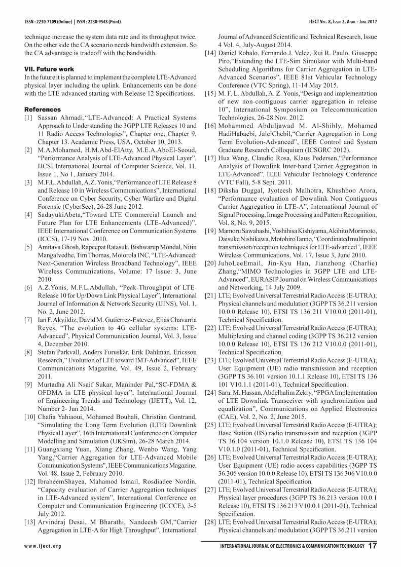
1. The mapperThe digital modulation constellation diagram represents the Mapper with type M-QAM with M= 16. The Mapper input is the certain logic values that are the output data from the Scrambler block. This input is assigned by the baseband symbols; which are the I and Q components. Where I is the in-phase component and Q is the quadrature component. Fig. 19 shows the simulation results of the Mapper block.
Fig. 19: Results of the 16-QAM mapper.
2. DE-mapperThe DE-Mapper block at the receiver has the reverse operation of the Mapper block at the transmitter. The DE-Mapper input is the complex QAM symbols that are received from the DE-Scrambler block. Fig. 20 shows the testing results of the De-mapper block where the complex QAM symbols are represented by the I and Q values and the output is four bits for every symbol.
Fig. 20: The Testing Results of the De-mapper Sub Block.
G. The Layer mapping and DE-Layer mapping and The Precoding blocksThe Layer Mapping block function is to map the complex-valued modulation symbols that are the output from the Mapper block to one or several transmission layers (antenna ports). For 2x2 MIMO system, the Layer Mapping block distributes the complex-valued modulation symbols between two transmission layer with two code words according to release 10 specifications (table 6.3.3.2-1 in section 6.3.3.2) [21].The function of the Pre-coding block is to multiply the complex-valued modulation symbols on each layer by a specific matrix for the data to be transmitted from the two antenna ports simultaneously. The linear combination of the two data streams at the two receiver antennas results in a set of two equations and two unknowns, which are resolvable into the two original data streams. The pre-coding matrix is applied according to release 10 specification (table 6.3.4.2.3-1 in section 6.3.4.2.3) [21]. Fig. 21 and Fig. 22 show the final results of the Pre-coding block form two layers.
Fig. 21: The Precoding Final Results From Layer One
Fig. 22: The Precoding Final Results From Layer Two
H. The Resource Element Mapping and DE-MappingThe Pre-coding symbols to be transmitted by the antenna ports are mapped to the resource elements block. The number of the available resource blocks is a function of the channel bandwidth as shown in Table 2.
Table 2: The Resources Block for Different Channel Bandwidth [23].
For the chosen LTE-A configuration, at 3MHz bandwidth the system have 15 resource block (RB), each one contain 12 subcarriers, then the total effective subcarrier number is 180 subcarrier (the number of the system RB multiple by the number of subcarriers in each RB). According to the Downlink resource grid shown in Fig. (6.2.2-1) in the LTE-A specification [21], it is implemented by generating a RAM of length 256 words and width of 22 bits. According to the specifications, a total of 180 locations is used, and the remaining locations are filled by zeros. We use a RAM length of 256 for the next IFFT block. The size of the IFFT block must equal to 2n, where n is an integer. So, the nearest size for the IFFT for the 180 sub-carrier is 28=256. Then we have 76 (256-180) free sub-carriers so, the RAM was filled by 38 zeros at the beginning and at the end of the OFDM symbol. The data are located at the middle of the RAM. The test results of the implemented data are shown in Fig. 23a, b and c.
Fig. 23(a): The RAM 38 Zeros at the Beginning
Fig. 23(b): The Data in the Middle of RAM.
IJECT Vol. 8, IssuE 2, AprIl - JunE 2017 Issn : 2230-7109 (online) | Issn : 2230-9543 (Print)
w w w . i j e c t . o r g 14 InternatIonal Journal of electronIcs & communIcatIon technology
Fig. 23(c): The RAM 38 zeros at the end.
I. The OFDM Signal GenerationThe next stage after The Resource element Mapping is the OFDM block. The OFDM block consists of an IFFT block and cyclic prefix insertion that is shown in Figure 24.
Fig. 24: The OFDM Block Diagram
The following sub-section introduces the implementation of the IFFT block, the Cyclic Prefix sub-block (OFDM), the cyclic prefix removal block and the FFT sub-block (DE-OFDM).
1. IFFT and Cyclic Prefix Sub BlockThe last two operations of the transmitter are the IFFT and the Cyclic Prefix (CP) insertion. The function of the IFFT block is to increase the bandwidth spectral efficiency by using the orthogonal frequency division while the function of the CP insertion block is to prevent the transmitted data from the Inter-Symbol Interference (ISI) and the Inter-Carrier Interference (ICI). The IFFT block (with a size of 256) and the CP insertion was implemented using Xilinx core. According to Release 10 specification, the last 144 samples in the OFDM symbol (for short CP) we will be copied at the start of it. Fig. 25(a) and Fig. 25(b) show the implementation results of the IFFT Xilinx core. Fig. 26 shows the simulation results of the Cyclic Prefix process.
Fig. 25(a): The Input to the IFFT Block
Fig. 25(b): The Output From the IFFT Block.
Fig. 26: The Cyclic Prefix process.
2. Cyclic Prefix Removal and FFTsub BlockAt the receiver, the cyclic prefix removal and FFT blocks have the reverse operations of the OFDM block at the transmitter. The CP removal sub-block removes the first 144 samples of the received OFDM symbol. The FFT block is implemented using a Xilinx generating core. Fig. 27 shows the simulation results of the FFT Xilinx core.
Fig. 27: The output from FFT block.
J. Time and Frequency Synchronization BlocksThe first two blocks in the receiver are the Time and Frequency Synchronization blocks. The function of the Time Synchronization block is to determine the start of the OFDM symbol while the function of the Frequency Synchronization block is to detect the frequency offsets that occurs due to the channel effects (like the Doppler shift and the carrier frequency mismatching between the transmitter and receiver oscillators). To determine the Time and Frequency Synchronization values we will depend on the fact that the last 144 samples in the OFDM symbol are repeated in the start as shown in Fig. 28.
Fig. 28: OFDM Symbol
The Synchronization process is done by correlating the received symbols with its delayed version by the OFDM symbol time T then repeating this operation 144 times (CP length) to calculate the summation of the resultant values each time to get the correlation value at this point. Then we will shift one bit in the received symbol and repeated the previous correlation process. Then, the max correlation result is chosen and putted in the polar form. The amplitude and the phase at the max correlation value represent the OFDM start position and the frequency offset values respectively. Fig. 29 shows the correlation process to obtain the Time and Frequency Synchronization values. The received OFDM symbol is delayed by the OFDM symbol time T. The following equation is used to calculate the correlation output X (t):
IJECT Vol. 8, IssuE 2, AprIl - JunE 2017
w w w . i j e c t . o r g InternatIonal Journal of electronIcs & communIcatIon technology 15
Fig. 29: Frequency and Timing Synchronization Through Cross Correlation
The Time and Frequency Synchronization processes are designed and implemented by using the VHDL codes. The following sub-sections are introducing the implementation of the Time and Frequency Synchronization blocks.
1. The Time Synchronization Block SimulationThe Register-Transfer Level (RTL) Schematic and the simulation results of the time synchronization block are shown in fig. 30 and fig. 31 respectively. It is clear that the start of the OFDM symbol was detected at sample number 144 as it should be.
Fig. 30: The Time Synchronization RTL Schematic.
Fig. 31: The Time Synchronization Block Testing Results.
2. The Frequency Synchronization Block SimulationThe RTL Schematic and the testing results of the Frequency Synchronization block are shown in Fig. 32 and Fig. 33 respectively.
By notice, the simulation result figures the value of the frequency offset is zero because there no channel effects are applied.
Fig. 32: The Frequency Synchronization RTL Schematic.
Fig. 33: The Frequency Synchronization Testing Results
III. The Full System VerivicationThe overall system verification is done by comparing the transmitter input to the receiver output with no channel effects. The transmitter input was represented by two OFDM symbols of 192 bits length and have the pattern 0101010……01010. Fig. 34 shows the Transmitter input while fig. 35 shows the Receiver output data. It is clear that the transmitter input coincides with the receiver output. Then the full system verification is done.
Fig. 34: The Transmitter Input
Fig. 35: The Receiver Output.
IJECT Vol. 8, IssuE 2, AprIl - JunE 2017 Issn : 2230-7109 (online) | Issn : 2230-9543 (Print)
w w w . i j e c t . o r g 16 InternatIonal Journal of electronIcs & communIcatIon technology
IV. The System UtilizationAfter implementing all the building blocks of the transceiver on FPGA Virtex 6, it is interesting to get out chip utilization for the whole system. In the following sub-section, the full system utilization will be introduced for the downlink LTE-A baseband single carrier and it is area optimization strategy.
A. The Full System UtilizationThe single carrier baseband system (Transmitter and receiver) resources utilization table fromVirtex 6 FPGA is shown in Table 3. It is clear that the LTE-A physical layer utilizes a small fraction of the resource blocks from Virtex 6. As shown in the table the number of used slice registers and the number of the look-up tables (LUTs) are very small, 1% and 4% respectively. The number of fully LUT-FF pairs (utilization efficiency) is high (62 %); which means a good utilization of the FPGA resources comparing by the previous design in [24].
Table 3: The Full System Utilization on Virtex 6.
B. The Area Optimization UtilizationFrom Xilinx ISE Design Suite 13.3 Design Goals and Strategies, the area optimization strategy was simulated. Table 4 shows the full system utilization by applying the area reduction design goal. By comparing the full system utilization table mentioned in the previous sub-section and the full system utilization table with area reduction strategy we notice that the numbers of slice registers is reduced from 3991 to 3968 and the slice LUTs are reduced from 6383 to 5567. Also there is an increase in the utilization efficiency (the number of fully LUT-FF pairs) from 62% to 71%.
Table 4: The full system utilization on Virtex 6 with the area reduction design goal.
V. The Carrier Aggregation scenario To increase the data rates and system capacity the Intra-band contiguous carrier aggregation scenario was applied. Two Component Carriers (CCs) are aggregated to double the system data rate. Fig. 36 shows the definition of aggregated channel bandwidth, aggregated channel bandwidth edges and the channel bandwidth for the contiguously aggregated component carriers.
The Downlink LTE-A simulation is designed to support 6 MHz CA with two CCs each one has a 3 MHz as a bandwidth. The center of the aggregated carriers shifted to baseband (0 Hz) and the center of two Component Carriers is -1.5 and 1.5MHz respectively. The simulation of CA scenario is done by using Matlab codes, to plot the CA power spectrum, because the VHDL simulator gives the frequency components values but the simulator is unable to plot the components spectrum. The CA calculation parameters are determined according to 3GPP release 10 sections (5.6 and 5.7) [23]. Fig. 37 shows the Power Spectrum simulation using the Matlab program for the CCs. The CA Matlab simulation parameters are shown in fig. 38.
Fig. 37: The Power Spectrum of the Component Carriers
Fig. 38: The Matlab Simulation Parameters for the Two CCs.
VI. ConclusionIn this paper, a complete LTE-advanced downlink physical layer transceiver with 2x2 MIMO technique and the Intra-band contiguous CA type has been designed and implemented according to the 3GPP Release 10 specification. All the stages of the LTE-Advanced Release 10 downlink physical layer, including the transmitter and the receiver, are modeled using Xilinx® ISE® Design Suite version 13.3 and implemented on Virtex 6 XC6VLX240T FPGA kit. The implemented building blocks include the time and frequency synchronization function in the receiver. It was found that the whole LTE-Advanced downlink physical layer consumes a small fraction of all the logic blocks. Moreover, the application of the CA scenario and the 2x2 MIMO
IJECT Vol. 8, IssuE 2, AprIl - JunE 2017
w w w . i j e c t . o r g InternatIonal Journal of electronIcs & communIcatIon technology 17
technique increase the system data rate and its throughput twice. On the other side the CA scenario needs bandwidth extension. So the CA advantage is tradeoff with the bandwidth.
VII. Future workIn the future it is planned to implement the complete LTE-Advanced physical layer including the uplink. Enhancements can be done with the LTE-advanced starting with Release 12 Specifications.
References[1] Sassan Ahmadi,“LTE-Advanced: A Practical Systems
Approach to Understanding the 3GPP LTE Releases 10 and 11 Radio Access Technologies”, Chapter one, Chapter 9, Chapter 13. Academic Press, USA, October 10, 2013.
[2] M.A.Mohamed, H.M.Abd-ElAtty, M.E.A.AboEl-Seoud, “Performance Analysis of LTE-Advanced Physical Layer”, IJCSI International Journal of Computer Science, Vol. 11, Issue 1, No 1, January 2014.
[3] M.F.L. Abdullah, A.Z. Yonis,“Performance of LTE Release 8 and Release 10 in Wireless Communications”, International Conference on Cyber Security, Cyber Warfare and Digital Forensic (CyberSec), 26-28 June 2012.
[4] SadayukiAbeta,“Toward LTE Commercial Launch and Future Plan for LTE Enhancements (LTE-Advanced)”, IEEE International Conference on Communication Systems (ICCS), 17-19 Nov. 2010.
[6] A.Z.Yonis, M.F.L.Abdullah, “Peak-Throughput of LTE-Release 10 for Up/Down Link Physical Layer”, International Journal of Information & Network Security (IJINS), Vol. 1, No. 2, June 2012.
[7] Ian F. Akyildiz, David M. Gutierrez-Estevez, Elias Chavarria Reyes, “The evolution to 4G cellular systems: LTE-Advanced”, Physical Communication Journal, Vol. 3, Issue 4, December 2010.
[8] Stefan Parkvall, Anders Furuskär, Erik Dahlman, Ericsson Research,” Evolution of LTE toward IMT-Advanced”, IEEE Communications Magazine, Vol. 49, Issue 2, February 2011.
[9] Murtadha Ali Nsaif Sukar, Maninder Pal,“SC-FDMA & OFDMA in LTE physical layer”, International Journal of Engineering Trends and Technology (IJETT), Vol. 12, Number 2- Jun 2014.
[10] Chafia Yahiaoui, Mohamed Bouhali, Christian Gontrand, “Simulating the Long Term Evolution (LTE) Downlink Physical Layer”, 16th International Conference on Computer Modelling and Simulation (UKSim), 26-28 March 2014.
[11] Guangxiang Yuan, Xiang Zhang, Wenbo Wang, Yang Yang,“Carrier Aggregation for LTE-Advanced Mobile Communication Systems", IEEE Communications Magazine, Vol. 48, Issue 2, February 2010.
[12] IbraheemShayea, Mahamod Ismail, Rosdiadee Nordin, “Capacity evaluation of Carrier Aggregation techniques in LTE-Advanced system”, International Conference on Computer and Communication Engineering (ICCCE), 3-5 July 2012.
[13] Arvindraj Desai, M Bharathi, Nandeesh GM,“Carrier Aggregation in LTE-A for High Throughput”, International
Journal of Advanced Scientific and Technical Research, Issue 4 Vol. 4, July-August 2014.
[14] Daniel Robalo, Fernando J. Velez, Rui R. Paulo, Giuseppe Piro,“Extending the LTE-Sim Simulator with Multi-band Scheduling Algorithms for Carrier Aggregation in LTE-Advanced Scenarios”, IEEE 81st Vehicular Technology Conference (VTC Spring), 11-14 May 2015.
[15] M. F. L. Abdullah, A. Z. Yonis,“Design and implementation of new non-contiguous carrier aggregation in release 10”, International Symposium on Telecommunication Technologies, 26-28 Nov. 2012.
[16] Mohammed Abduljawad M. Al-Shibly, Mohamed HadiHabaebi, JalelChebil,“Carrier Aggregation in Long Term Evolution-Advanced”, IEEE Control and System Graduate Research Colloquium (ICSGRC 2012).
[17] Hua Wang, Claudio Rosa, Klaus Pedersen,“Performance Analysis of Downlink Inter-band Carrier Aggregation in LTE-Advanced”, IEEE Vehicular Technology Conference (VTC Fall), 5-8 Sept. 2011.
[18] Diksha Duggal, Jyoteesh Malhotra, Khushboo Arora, “Performance evaluation of Downlink Non Contiguous Carrier Aggregation in LTE-A”, International Journal of Signal Processing, Image Processing and Pattern Recognition, Vol. 8, No. 9, 2015.
[20] JuhoLeeEmail, Jin-Kyu Han, Jianzhong (Charlie) Zhang,“MIMO Technologies in 3GPP LTE and LTE-Advanced”, EURASIP Journal on Wireless Communications and Networking, 14 July 2009.
[21] LTE; Evolved Universal Terrestrial Radio Access (E-UTRA); Physical channels and modulation (3GPP TS 36.211 version 10.0.0 Release 10), ETSI TS 136 211 V10.0.0 (2011-01), Technical Specification.
[22] LTE; Evolved Universal Terrestrial Radio Access (E-UTRA); Multiplexing and channel coding (3GPP TS 36.212 version 10.0.0 Release 10), ETSI TS 136 212 V10.0.0 (2011-01), Technical Specification.
[23] LTE; Evolved Universal Terrestrial Radio Access (E-UTRA); User Equipment (UE) radio transmission and reception (3GPP TS 36.101 version 10.1.1 Release 10), ETSI TS 136 101 V10.1.1 (2011-01), Technical Specification.
[24] Sara. M. Hassan, Abdelhalim Zekry, “FPGA Implementation of LTE Downlink Transceiver with synchronization and equalization”, Communications on Applied Electronics (CAE), Vol. 2, No. 2, June 2015.
[25] LTE; Evolved Universal Terrestrial Radio Access (E-UTRA); Base Station (BS) radio transmission and reception (3GPP TS 36.104 version 10.1.0 Release 10), ETSI TS 136 104 V10.1.0 (2011-01), Technical Specification.
[26] LTE; Evolved Universal Terrestrial Radio Access (E-UTRA); User Equipment (UE) radio access capabilities (3GPP TS 36.306 version 10.0.0 Release 10), ETSI TS 136 306 V10.0.0 (2011-01), Technical Specification.
[27] LTE; Evolved Universal Terrestrial Radio Access (E-UTRA); Physical layer procedures (3GPP TS 36.213 version 10.0.1 Release 10), ETSI TS 136 213 V10.0.1 (2011-01), Technical Specification.
[28] LTE; Evolved Universal Terrestrial Radio Access (E-UTRA); Physical channels and modulation (3GPP TS 36.211 version
IJECT Vol. 8, IssuE 2, AprIl - JunE 2017 Issn : 2230-7109 (online) | Issn : 2230-9543 (Print)
w w w . i j e c t . o r g 18 InternatIonal Journal of electronIcs & communIcatIon technology
[29] LTE; Evolved Universal Terrestrial Radio Access (E-UTRA); Multiplexing and channel coding (3GPP TS 36.212 version 11.0.0 Release 11), ETSI TS 136 212 V11.0.0 (2012-10), Technical Specification.
[30] LTE; Evolved Universal Terrestrial Radio Access (E-UTRA); Physical layer procedures (3GPP TS 36.213 version 11.0.0 Release 11), ETSI TS 136 213 V11.0.0 (2012-10), Technical Specification.
[31] LTE; Evolved Universal Terrestrial Radio Access (E-UTRA); Physical layer; Measurements (3GPP TS 36.214 version 11.0.0 Release 11), ETSI TS 136 214 V11.0.0 (2012-10), Technical Specification.
Sara M. Hassan She received the B.Sc. degree in Electrical Engineering from Modern academy for engineering and technology, Cairo, Egypt, in 2007, and the M. Sc. degree in Advanced Mobile Communication Techniques from Ain Shams University, Cairo, Egypt, in 2013.She is currently a PhD. student in the Department of Electronics and Communications Engineering at Ain Shams University. Her general research
interests include design and implementation for Building Blocks in Advanced Mobile Communication Techniques, and currently her research work focuses on LTE-Advanced transceivers.
Abdelhalim Zekry is a professor of electronics at faculty of Engineering, Ain Shams University, Egypt. He worked as a staff member on several universities. He published more than 160 papers. He also supervised more than 70 Master thesis and 25 Doctorate. Prof. Zekry focuses his research programs on the field of microelectronics and electronic applications including communications and photovoltaics. He got several
prizes for his outstanding research and teaching performance.