234
Self Learning Material Computer System Architecture (BSIT 301) Course: Bachelor of Science (IT) Semester-III Distance Education Programme I.K. Gujral Punjab Technical University Jalandhar

Self Learning MaterialComputer System Architecture
(BSIT 301)
Course: Bachelor of Science (IT)
Semester-III
Distance Education Programme
I.K. Gujral Punjab Technical University
Jalandhar
SyllabusI.K. Gujral Punjab Technical University
Scheme of (BScIT)Batch 2015 Onwards
BSIT 301 COMPUTER SYSTEM ARCHITECTUREMax. Marks: 100
External Assessment: 60Internal Assessment: 40
Objectives: To make students aware about the basic building blocks of computer systemand how the different components are interfaced together. Students will know about thebasic functioning of various parts of computer system from hardware point of view andinterfacing of various peripheral devices used with the system.
UNIT IIntroduction to Computer Architecture: Introduction to Computer and CPU (ComputerOrganization, Computer Design and Computer Architecture), Stored Program Concept- VonNeumann Architecture. Introduction to Flynn‟s Classification- SISD, SIMD, MIMDRegister Transfer and Micro operations- Introduction to Registers, Register TransferLanguage, Data movement among Registers and Memory.Micro operations: Introduction to micro operations, Types of micro operations--LogicOperations, Shift operations, Arithmetic and Shift operations.Common Bus System : Introduction to Common Bus System, Types of Buses(Data Bus,Control Bus, Address Bus), 16 bit Common Bus System--Data Movement among registersusing Bus.
UNIT IIBasic Computer Instructions- Introduction to Instruction, Types of Instructions (MemoryReference, I/O Reference and Register Reference), Instruction Cycle, Instruction Formats(Direct and Indirect Address Instructions, Zero Address, One Address, Two Address andThree Address Instructions)Interrupt: Introduction to Interrupt and Interrupt Cycle.Design of Control Unit: Introduction to Control Unit, Types of Control Unit (Hardwired &Micro programmed Control Unit).Addressing Modes-Introduction & different types of Addressing Modes.
UNIT IIII/O Organization: I/O Interface Unit, types of ports (I/O port, Network Port, USB port, Serialand Parallel Port), Concept of I/O bus, Isolated I/O versus Memory Mapped I/O.I/O Data Transfer Techniques: Programmed I/O, Interrupt Initiated I/O, DMA Controllerand IOP.Synchronous and Asynchronous Data Transfer: Concept of strobe and handshaking,source and destination initiated data transfer.
UNIT IVStack Organization: Memory Stack and Register StackMemory organization: Memory Hierarchy, Main Memory (RAM and ROM chips, Logicaland Physical Addresses, Memory Address Map, Memory Connection to CPU), AssociativeMemoryCache Memory: Cache Memory (Initialization of Cache Memory, Writing data into Cache,Locality of Reference, Hit Ratio), Replacement Algorithms (LRU and FIFO).Cache Memory Mapping Techniques: Direct Mapping, Associative Mapping and Set-Associative Mapping. Harvard Architecture, Mobile Devices Architecture (Android, Symbianand Windows Lite), Layered Approach Architecture.
Suggested Readings / Books:1. Computer System Architecture, M.M. Mano, Third Edition, PHI2. Computer Organization and Architecture, J.P. Hayes, Third Edition, TMH3. Computer Organization and Architecture, Stallings, Eighth Edition, PHI
Table of Contents
Chapter No. Title Written By Page No.1 Introduction to Computer
ArchitectureEr. Naveen DograAssistant Professor (CSE)Punjab University,SSGR Campus,Hoshiarpur
1
2 Register Transfer and MicroOperations
Er.Balwant RajAssistant Professor (ECE)Punjab University,SSGR Campus,Hoshiarpur
19
3 Micro operations Er.Balwant RajAssistant Professor (ECE)Punjab University,SSGR Campus,Hoshiarpur
37
4 Common Bus SystemMs. Shipra Chopra,Assistant professor,DAV College,Jalandhar
58
5 Basic Computer Instructions Er.Balwant RajAssistant Professor (ECE)Punjab University,SSGR Campus,Hoshiarpur
72
6 Interrupt Er. Naveen DograAssistant Professor (CSE)Punjab University,SSGR Campus,Hoshiarpur
87
7 Design of Control Unit Er. Naveen DograAssistant Professor (CSE)Punjab University,SSGR Campus,Hoshiarpur
106
8 Addressing Modes Er.Balwant RajAssistant Professor (ECE)Punjab University,SSGR Campus,Hoshiarpur
116
9 Input/Output (I/O) Organisation Er.Neeraj SharmaAssistant Professor (ECE)Punjab University,SSGR Campus,Hoshiarpur
136

10 I/O Data Transfer Techniques Dr. Satish kumarAssociate ProfessorMCA Deptt.,Punjab University,
SSGRCampus,
Hoshiarpur
150
11 Synchronous and AsynchronousData Transfer
Dr. Satish kumarAssociate ProfessorMCA Deptt.,Punjab University,SSGRCampus,Hoshiarpur
162
12 Stack Organization Mr.Rajinder SinghAssistant Professor, MCAPunjab University,SSGR Campus,Hoshiarpur
171
13 Memory Organization Mr.Rajinder SinghAssistant Professor, MCAPunjab University,SSGR Campus,Hoshiarpur
Mr.Rajinder SinghAssistant Professor, MCAPunjab University,SSGR Campus,Hoshiarpur
183
14 Cache MemoryMr.Rajinder SinghAssistant Professor, MCAPunjab University,SSGR Campus,Hoshiarpur
194
15 Cache Memory MappingTechniques
Mr.Rajinder SinghAssistant Professor, MCAPunjab University,SSGR Campus,Hoshiarpur
201
16 Mobile Devices ArchitectureMs. Shipra ChopraAssistant Professor,DAV College,Jalandhar
208
Reviewed by:
Er. Gurpreet Singh BainsDepartment of Electronics and Communication Engineering,
PUSSG Regional Campus, Hoshiarpur
© IK Gujral Punjab Technical University JalandharAll rights reserved with IK Gujral Punjab Technical University Jalandhar
1
Lessons 1
Introduction to Computer Architecture
Structure
1.0 Objectives
1.1 Introduction
1.2 Basic of Computer
1.3 Von Neumann Architecture
1.4 CPU Organization
1.5 Summary
1.6 Glossary
1.7 Answer to Check Your Progress/Suggested Answers to SAQ
1.8 Bibliography/ References/ Suggested Readings
1.9 Terminal and Model Questions
1.0 Objectives
After studying this chapter you will understand
The basic structure of computer system.
Conversion of binary number to decimal number.
Organization of the CPU.
Computer Architecture and Computer organization.
Flynn’s classification of parallel systems.

2
1.1 Introduction
This chapter provides the information about the basic structure of computer systems. Thecomputer is consisting up to electromechanical components. Now a day, digital computer usesthe binary system for computation. Many computer manufacturing companies are providingcomputer models with the same architecture but different organization. Computer architectureattributes are visible to the programmer whereas organization refers to operational units of thecomputer system and also how these units are interconnected. Chapter also discusses the VonNeumann architecture of the computer system. To facilitate the programming process, thisarchitecture uses the stored program concept. According to Neumann, computer consists up ofCentral processing unit, memory and input/output equipments. At end we also discuss theFlynn’s classification of the computer systems.
1.2 Basic of Computer
Computer is electromechanical device that takes input, process that input and providesus the desire results. The first digital computer was developed in late 1940s. The name of it wasENIAC (Electronic Numerical Integrator And Computer) and developed in the University ofPennsylvania. It uses digits (0,1,2,..9) for performing the numerical computation, that’s why theterm digital computer emerged. In practice, digital computer works more efficiently and reliablyif it uses two states only. This leads to the development of binary computer with two states:true and false.
Digital computers use binary number system consisting of binary digit: 0 and 1. A binary digit isalso called bit. Group of bits is used to represents the information. By using various codingmethod, the group of bits is used not only to represents binary numbers but also represents theother symbols such as digits, letters, and instructions. These instructions are used to performvarious types of computations. The decimal number system is base 10 system and binarysystem is of base 2 with digits 0 and 1. The binary number can be converted to decimal systemas follows.
For example binary number is 010001. It can be converted to decimal as
(0X25) + (1X24) + (0X23) + (0X22) + (0X21) + (1X20)
0 + 16 + 0 + 0 + 0 + 1 = (17)10
The study of computer system is subdivided in to two part hardware and software. Thehardware of computer system is consisting up of electronic or electromechanical parts such asmonitor, hard disk, I/O devices. The software components are instruction and data. Theinstructions manipulate the data and provide us the result. The sequence of instructions

3
performing specific task is called program. The data that is manipulated by the programconstitute the databases.
The software is further subdivided into system software and application software. The task ofthe system software is to make the efficient use of the computer. Operating systems anddatabases software are the example of system software. The application software is used tosolve a particular problems e.g. banking software, railways reservation software etc are comeunder this category. It is written in high level language and need to convert in to machinelanguage. Compiler is software that converts high level language to machine language. Systemsoftware is an indispensible part of a computer system.
The hardware of computer is mainly divided into three parts, Central Processing Unit (CPU),Memory and I/O components shown in figure 1. The CPU is used to process the data. Thememory of the computer is a storage unit. It stores the instructions and data. It is randomaccess in nature means it can access any location randomly. The I/O components are physical innature and use for communicating and controlling the transfer of information to and from thecomputer system and outside world. Block diagram of computer system is shown in figure1.
INPUT / OUTPUTCOMPONENTS
MAIN MEMORY
Instruction
Data
CPU
Figure 1: Main components of computer
4
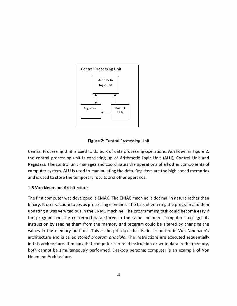
Figure 2: Central Processing Unit
Central Processing Unit is used to do bulk of data processing operations. As shown in Figure 2,the central processing unit is consisting up of Arithmetic Logic Unit (ALU), Control Unit andRegisters. The control unit manages and coordinates the operations of all other components ofcomputer system. ALU is used to manipulating the data. Registers are the high speed memoriesand is used to store the temporary results and other operands.
1.3 Von Neumann Architecture
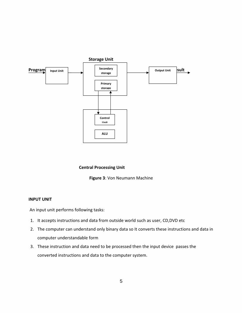
The first computer was developed is ENIAC. The ENIAC machine is decimal in nature rather thanbinary. It uses vacuum tubes as processing elements. The task of entering the program and thenupdating it was very tedious in the ENIAC machine. The programming task could become easy ifthe program and the concerned data stored in the same memory. Computer could get itsinstruction by reading them from the memory and program could be altered by changing thevalues in the memory portions. This is the principle that is first reported in Von Neumann’sarchitecture and is called stored program principle. The instructions are executed sequentiallyin this architecture. It means that computer can read instruction or write data in the memory,both cannot be simultaneously performed. Desktop persona; computer is an example of VonNeumann Architecture.
Central Processing Unit
Arithmeticlogic unit
Registers ControlUnit
5
Storage Unit
Program Result
Central Processing Unit
Figure 3: Von Neumann Machine
INPUT UNIT
An input unit performs following tasks:
1. It accepts instructions and data from outside world such as user, CD,DVD etc
2. The computer can understand only binary data so It converts these instructions and data in
computer understandable form
3. These instruction and data need to be processed then the input device passes the
converted instructions and data to the computer system.
Secondarystorage
Primarystorage
ControlUnit
ALU
Input Unit Output Unit

6
STORAGE UNIT
The storage unit performs following tasks:
1. Storage unit stores the data and instructions read from input device. These instructions are
required for processing the data.
2. It also stores the Intermediate results of processing.
3. The storage units is also required to store the final results of processing and then released
to an output device
There are two types of storage devices
Primary Storage
It is volatile in nature i.e. it loses it’s connect when power goes off.
It is used to store intermediate result of processing and also hold the data.
Since it is made up of semiconductor device, it is fast and very expensive.
Example of primary storage is RAM i.e. Random Access Memory
Secondary Storage
It is used to store the result permanently.
It holds data and information of stored jobs.
It is less expensive than primary memory.
Due to its cheaper cost it used or bulk storage.
It is non volatile in nature.
Example of Secondary Storage is Magnetic Tapes, Hard Disks and Flash drives.
CENTRAL PROCESSING UNIT (CPU)
It is the brain of computer System .It control and coordinates all the activities of the systems. It
consist up of following units.
Arithmetic Logic Unit (ALU)
7
Arithmetic Logic Unit of a computer system is the place where the actual executions of
instructions. It performs computer’s computational and logical functions on the operands.
Control Unit (CU)
Control unit control and coordinates the operations of all other components of computer
system. It performs certain tasks such as directing the fetching of instruction and data from the
memory. It also direct the output performed to output device.
OUTPUT UNIT
An output unit of a computer system performs the following functions:
1. It accepts the result of the computation performed by ALU. This result is in binary form.
2. It converts these coded results to human Readable form and show the result to outside
world.
Monitors and Printers are the example of output unit.
Self Assessment 1
Q1. Explain various parts of computer systems?
Sol.__________________________________________________________________________
__________________________________________________________________________
__________________________________________________________________________
__________________________________________________________________________
Q2. Convert 110011 binary number into decimal number?
Sol.__________________________________________________________________________
8
__________________________________________________________________________
__________________________________________________________________________
Q3. Differentiate between primary memory and secondary memory?
Sol.__________________________________________________________________________
__________________________________________________________________________
__________________________________________________________________________
__________________________________________________________________________
Q4. CPU stands for __________.
Q5. The first computer was developed is ______.
1.4 CPU Organization
To understand the organization of CPU, firstly we should understand that how the instruction isexecuted in the processor. For executing the instruction the processor must do:
Fetch instruction
Decode instruction
Execute instruction
During the fetch operation the processor reads an instruction from the memory, than aninstruction is decoded to determine but action should be taken. If the data is present within theinstruction then it is executed and result is written back into the memory, but if the instructionrequired operand for execution, then the operand is first read from the memory address andthen required operation is performed.
To do these things processor needs:
Registers to store temporary data.

9
Register to store the address of next instruction to be executed.
Needs to store instruction and data temporarily when the instruction is executing.
Components for performing computational tasks.
Components for controlling overall operations.
System bus for interconnection.
Figure 4 shows the basic structure of CPU
Interface to and from memory or I/O devices
Figure 4: Basic Structure of CPU
Data Processing Unit
ALU
Accumulator(AC)
Program Control Unit
Instructionregister
ProgramCounter
Control unit
DataRegister
(DR)
MemoryAddressRegister(MAR)
Internal CPU Bus

10
Accumulator (AC):
The accumulator register store one of the operands. It interacts with the ALU and aftercomputation store the output temporarily.
Arithmetic and Logic Unit (ALU):
ALU is the main part of CPU. It performs various arithmetic and logical computations and storeresult back in the main memory.
Program Counter (PC):
The PC contains the address of next instruction to fetch from memory.
Memory Address Register (MAR):
The address generated in the PC moved to MAR. So MAR provide the address of memory fromwhere the instruction is retrieved.
Data Register (DR):
When a memory is address by MAR, then control units request for memory read, the results isplaced on data bus and then into the DR. So we can say the DR contains a word or data to beread from memory or to written into the memory.
Instruction Register (IR):
It contains the instruction that is most recently fetched. The instruction that is present in DR isloaded into the IR.
Control Unit (CU):
It control and coordinate all the activities of the system.
1.5 Organization and Architecture
When dealing with the hardware of computer system we must distinguish between computerorganization, computer design and computer architecture.
Computer organization is the study of the operations of hardware components and how thesecomponents are connected together to form a computer. The task of the organizationalstructure is to check the various components operate as they intended to do. The

11
organizational attributes includes memory technology, control signals, interface betweencomputer and peripherals.
Computer Design is the hardware design of computer system. Once the specifications of thecomputer are formulated, it is the task of designer to develop the hardware for the system.Computer design is concerned with to find which hardware should be used and how thedifferent parts should be connected.
Computer architecture is concerned with structure and behaviour of computer system as peruser perspective. It includes the instruction formats, instruction set, information, I/Omechanism and addressing modes. It also includes the attributes that have direct impact onexecution of program.
For example, it is an architectural issue that computer will have multiply instruction. How thismultiplication is implemented, it is an organizational issue. Multiplication can be implementedwith special multiplication unit or the by repeated use of the add unit mechanism. Theorganizational decision is based on the frequency of multiply instruction used, comparison ofspeed among the two approaches, cost of special multiply unit. The computer manufacturer’soffers computer models with same architecture but different models.
.
1.6 Parallel Processing
Parallel Processing is a technique that is used to provide simultaneous processing of data. Themain purpose of parallel prosessing is to increase the speed of processing and also to increasethe throughput i.e. number of instruction executed in per unit time. Traditionally thecomputers process the insturctions sequentially; a parallel processing sytem is able to performthe concurrent data processing. For example when an ALU is executing an instruction, the nextinstuction can be read from the memory. The computer system may have two or more ALUs toexecute two or more instruction simualtationally. There is various level of complexity in theparallel processing but at the lowest level we distinguish between parallel and serial operationsby the type of register being used. Shift register operates in serial manner, but the registerswith parallel load operation, operate all the bits of the word simultaneously. At the higher levelof complexity parallel processing is achieved by the multiple functional units that performidentical tasks or different tasks simultaneously. As the hardware increases with the parallelprocessing, the cost of the system also increases. But the technological advancement hasreduced the harware cost, so parallel processing became feasible.
Classification of parallel processing

12
The classification of parallel processing is based on:
1. Internal organization of processors
2. Interconnection structure between the system
3. Flow of information through the system
M.J.Flynn categorizies the computer systems by number of instructions and data itemsprocessed simultaneously. The normal operation of the computer is to fetch instruction fromthe memory, execute it in the processor and then places its final result back in the memory.
Instruction Stream
Data Stream
Figure 3: Streams in the computer
Instruction stream: the sequence of instructions read from memory constitutes the instructionstream. It is one dimensional only.
Data stream: the processor performs operations on the data and constitutes the data stream.Data flows to and from the processor.
The parallel processing may occur in instruction stream, in the data stream or both ininstruction stream or data stream.
Flynn’s classification divides computers into four broad groups based on the instruction streamand data streams:
1. Single instruction stream, single data stream (SISD)
2. Single instruction stream, multiple data stream (SIMD)
3. Multiple instruction streams, single data stream (MISD)
4. Multiple instruction stream, multiple data stream (MIMD)
Single instruction stream, single data stream (SISD) represents the organization ofconventional computer system with a control unit (CU), a processor unit (PU) and a memoryunit (MU). Instructions are executed sequentially. A processor executes single instructionstream (IS) on data stored in single memory. Parallel processing in SISD is achieved by multiple
Processor(P)
Memory(M)

13
functional units or by pipelining. Uniprocessors are example of this category of computersystems.
IS DS
Figure 4: SISD
Single instruction stream, multiple data stream (SIMD) represents an organization ofcomputer system with multiple processing units works under the supervision of commoncontrol unit. A single machine instruction controls the simultaneous execution of all theprocessors. A shared memory unit partitioned into multiple modules so that it maycommunicates with all the processor units. Vector and Array processors are the example ofSIMD.
Figure 5: SIMD
PU1 DS LM1
CU IS PU2 DS LM2
: :
PUn DS LMn
CU PU MU
14
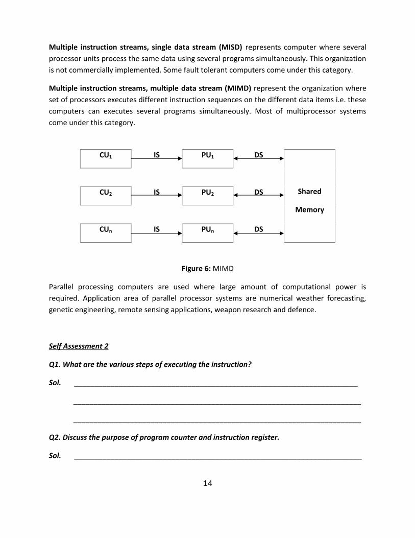
Multiple instruction streams, single data stream (MISD) represents computer where severalprocessor units process the same data using several programs simultaneously. This organizationis not commercially implemented. Some fault tolerant computers come under this category.
Multiple instruction streams, multiple data stream (MIMD) represent the organization whereset of processors executes different instruction sequences on the different data items i.e. thesecomputers can executes several programs simultaneously. Most of multiprocessor systemscome under this category.
Figure 6: MIMD
Parallel processing computers are used where large amount of computational power isrequired. Application area of parallel processor systems are numerical weather forecasting,genetic engineering, remote sensing applications, weapon research and defence.
Self Assessment 2
Q1. What are the various steps of executing the instruction?
Sol. ______________________________________________________________________
_______________________________________________________________________
_______________________________________________________________________
Q2. Discuss the purpose of program counter and instruction register.
Sol. _______________________________________________________________________
CU1 IS PU1 DS
Shared
Memory
CU2 IS PU2 DS
CUn IS PUn DS
15
_______________________________________________________________________
_______________________________________________________________________
Q3. What do you understand by computer organization?
Sol. ________________________________________________________________________
_________________________________________________________________________
_________________________________________________________________________
_________________________________________________________________________
Q4. The SIMD stands for _______________________________.
Q5. The MIMD stands for _______________________________.
2.7 Summary
Computer system had solved our problem to perform large computational task with accuracy.Study of computer is mainly dividing into two parts, hardware and software. Hardware is thephysical part of the system and the actual calculation work is done by the hardware. The centralprocessing unit, memory and I/O components constitute the hardware part of system. Thesoftware is the logical part, and it instructs the physical part to carry out calculations and otherworks. Today’s computer architecture is based on the Von Neumann architecture. It uses thestored program concept for making the programming task easy.
Central processing unit is consists up of ALU, Memory unit and processor registers. Theregisters are also called high speed memories and they are used for storing data andinstructions while executing. The program counter contains the address of next instruction forexecution. The IR register stores the currently executing instruction. Accumulator stores one ofthe operands and in many cases it also stores the result that is to be stored in the memory. Theother registers that are used are data register, memory address register etc.
As the computer industry has matured, the various techniques to increase the processing speedhave been evolved. Parallel Processing is a technique that is used to provide simultaneousprocessing of data. The main purpose of parallel processing is to increase the speed ofprocessing and also to increase the throughput. M.J.Flynn categorizes the computer systems by
16
number of instructions and data items processed simultaneously. According to Flynn theparallel computers are divided into 4 categories i.e. SISD, SIMD, MISD, and MIMD.
1.8 Glossary
Accumulator: The accumulator (AC) register store one of the operands. It interacts withthe ALU store temporary results.
Arithmetic Logic Unit: Arithmetic and logic unit perform all the arithmetic and logicaloperations.
Central Processing Unit: It is the brain of computer. Its main aim is to control andCoordinates all activities of system.
Data Stream: The processor performs operations on the data and constitutes the datastream.
Instruction Register: It contains the instruction that is most recently fetched. Theinstruction that is present in DR is loaded into the IR.
Instruction Stream: the sequence of instructions read from memory constitutes theinstruction stream.
MIMD: It is a notation for multiple instructions stream multiple data stream Most ofmultiprocessor systems come under this category.
Program: Program is a set of instruction to do a specific task. Program Counter: The program counter (PC) stores the address of next instruction in
the program and it is used during the fetch phase. RAM: It is a Random Access memory. It is also called the main memory of system. SIMD: It is a notation for single instruction stream multiple data streams. Vector and
Array processors are the example of SIMD.
1.9 Answer to Check Your Progress/Suggested Answers to SAQ
Self Assessment 1
Solution 1) the various steps for executing the instruction are:1. Fetch instruction2. Decode instruction3. Execute instruction
.Solution 2)
(1X25) + (1X24) + (0X23) + (0X22) + (1X21) + (1X20)
17
32 + 16 + 0 + 0 + 2 + 1 = (51)10
Solution 3)
PRIMARY MEMORY SECONDARY MEMORY
It is volatile in nature.
It is made up of semiconductormaterial.
It is very expensive, since cost perbit storage is more.
It is very fast memory.
Example RAM
It is non volatile in nature.
It is made up to physical material.
It is less expensive.
It is slow as compare to primarymemory.
Example Hard disk, magneticmemory.
Solution 4) Central Processing Unit
Solution 5) ENIAC (Electronic Numerical Integrator And Computer)
1.10 Bibliography/ References/ Suggested Readings:
1. Computer System Architecture, M.M. Mano, Third Edition, PHI.2. Computer Organization and Architecture Lab.3. Computer Organization and Architecture, Stallings, Eighth Edition, PHI.
1.11 Terminal and Model Questions
Q1. Differentiate between hardware and software?
Q2. What is stored program concept?
Q3. Explain the various components of computer system.
18
Q4. Differentiate between computer architecture and computer organization?
Q5. What do you understand by fetch, decode and execute instructions?
Q6. Explain the processor registers in detail.
Q7. What do you understand by parallel processor? Explain different type of parallelprocessors.
Q8. Explain the SIMD array processor in detail.
19
Lesson 2
Register Transfer and Micro operations
Structure2.0 Objectives
2.1 Introduction
2.2 Registers
2.2.1 Shift Registers
2.3 Register Transfer Language
2.4 Self Assessment Questions (Section 2.1 to 2.3)
2.5 Data Transfer between Registers
2.5.1 Register Transfer with Control Condition
2.6 Bus System
2.6.1 Bus System design Using Multiplexer
2.6.2 Bus System Design Using Tri-State Buffers
2.7 Memory
2.7.1 Memory Transfer
2.8 Self Assessment Questions
2.9 Summary
2.10 Glossary
2.11 Answer to check your progress/Suggested Answers to SAQ
2.12 References/Bibliography/Suggested Readings
2.13 Model Questions and Problems
2.0 Objectives
Study the registers available in the computer architecture and their use.
Study of various Symbols for register transfer operations
Use of symbols for data transfer in between registers
Concept of bus structure

20
After the completion of this chapter students will be able to understand the basic concepts of
registers and set of symbols to perform various operations of data transfer between these
registers as well as memory. Study of various symbols used for representing various micro-
operations will help to proceed for the skill development to write the sequence of instructions
in symbolic form to perform various micro-operations.
2.1 Introduction
Data processing is done by digital systems that are designed using various digital hardware
modules. Digital systems that are used to process binary information can be as simple as a flip-
flop ( designed using few logic-gates ) to store one bit and these systems can be as complex as
digital signal processors in the integrated circuits (IC’s) form. Most of the digital computers are
designed using modular design approach. Individual digital circuits such as registers, arithmetic
and logic circuits, timing and control units, interrupt control units etc. are designed as individual
modules. These individual modules are the interconnected with each other using the common
bus system (internal data bus, address bus and control bus). The individual modules after the
interconnection with each other function as a single unit called a Central Processing Unit (CPU)
or a Digital Computer.
Internal hardware modules organization of the CPU can be specified as:
The group of registers and their functions
Sequencing of the micro-operations execution.
Timing and the control functions
2.2 Registers
To perform various operations, processor must have required some storage devices to save the
instructions (temporarily). Registers are the best suitable option for storing the instructions
fetched from the memory. A register is designed using a group of flip-flops. One flip-flop is
capable of storing one bit of information. An 8-bit register has a group of 8 flip-flops and is

21
capable of storing any binary information of 8 bits and so on i.e. number of flip flops required to
design a register depends on the number of bits to be stored in it.
In addition to the flip-flops, a register may be designed using the digital combinational circuits
using logic gates. Registers are designed using different methods as per their applicability in the
different applications. The simplest register is designed using only the flip-flops i.e. without
using any other logic gates. A four bit (A3A2A1A0) register designed using the D flip flops is
shown in Figure 2.1.
All flip flops are triggered at the same time on the rising edge of the clock applied at C input of
the flip flop. Data available in the flip flops is transferred to the register on the rising edge of
the clock. On the application of logic level 0 on the “Clear” input, all the flip flops gets reset, and
remains reset till the “Clear” pin of the flip flop is on the logic 0. In the registers the “Clear” input is used to clear
it’s all the bits to logic o. Here it must be noted that the signal applied on the “Clear” pin is independent of the
clock signal. The data to be loaded into the register is applied at the inputs (I3I2I1I0) and is available on the Q output
on the rising edge of the clock. As discussed n bit register can be designed using the n number of the D flip flops.
22
Figure 2.1 Hardware logic circuit of a 4 bit register
2.2.1 Shift Registers
Shift Registers are used to shift (move) binary data from one direction (left to right) to other or vice-versa (right to
left). Similar to the registers discussed in section 2.2, shift registers are also designed using the flip-flops
interconnected in the cascaded form. Serial input serial output shift register designed using four flip-flops is shown
in fig 2.2.

23
Figure
2.2 4-bit Shift register
This is the simplest possible design using D Flip-Flop. This type of shift register is used to shift a 4 bit number from
left to right on the application of a clock pulse simultaneous to all the flip-flops. Four bit data that is required to be
shifted from left to right is applied to at left most flip-flop (one bit at a time) and output is taken from Q output of
rightmost flip-flop. As shown in circuit of figure 2.2, when clock pulse is applied to all the flip-flop at C input, then
output of first (left most) flip-flop becomes Input of next flip-flop and so on. The shifting of data can be controlled
by applying clock pulse through the two input AND gate. Clock is applied at one input of this AND gate and a
control bit is applied at its other input. When shifting of bits is required, control bit of logic 1 is applied and when
no shifting is required control bit of logic 0 is applied. Thus clock ANDed with logic 0 gives output zero hence no
clock at C input means no shifting of bits takes place. Shift right shift register can also be designed on the same
pattern as shift left is designed.
2.3 Register Transfer Languages
Digital system or digital computer discussed in previous section is used to perform various operations such as
arithmetic, logic, data transfer, branching operations etc. The operations performed by the CPU on the data
(operand) stored in the registers or in the memory are called micro-operations. The result obtained after the
micro-operations, can replace the current contents of register or it can be saved to some other register or the
memory. The shift operations, data transfer, arithmetic and logic operations are the examples of the various
micro-operations.
The notations (in symbolic form such as numbers, alphabets, special characters etc.) used as micro-operations to
transfer data in between the registers available in the CPU is called register transfer language. As the english words
such as MOV, ADD, MUL, DIV etc. are used to perform an operation in the assembly language ,on the same pattern
the operations such as data transfer, arithmetic / logic etc. can be performed using the symbolic notations such as
R1(Register1), R2(Register2),
performed using such methods are called the Micro-operations. This method of writing sequence of instructions
(programs) is more convenient and previous concise and organized manner to write sequence of micro-operations.
Digital hardware logic circuits are used to implement / perform register transfer or other micro-operations.

24
Register transfer language in other terms is the group of micro-operations used to perform the data transfer from
one register to another within the processor. The “language” is a term used by the programmers who work in the
field of programming languages. Programming Language is a set of symbols written in a sequence to perform some
computational or data processing task. Symbols used in register transfer language are chosen as simple as possible
so that it should be easy to memorize. Various type of symbols used to perform micro-operations are discussed in
the next sections and hardware implementation of these micro-operations is also discussed side by side. Before
processing the sequencing of micro-operations in a complete program form, knowledge of the internal
architecture of the CPU is most i.e. availability of various registers and symbols used to represent them. Once
programmers are familiar with the programming concepts using these symbols, they can easily write programmers
using other set of symbols for different processors/CPU.
2.4 Self Assessment Questions (Section 2.1 to 2.3)
1. The operations performed on data stored in registers are called ___________
2. The decoded instruction is stored in ____________
3. For the execution of set of instructions which register gets initialized first?
a) Instruction Register
b) Program Counter
c) Memory Address Register
d) None of these
4. What do you mean by register transfer language?
5. __________is a basic memory element.
a. Tri state buffer
b. NAND Gate
c. Memory Address Register
d. Flip Flop
2.5 Data Transfer between Registers
Central processing unit of the computer system consists of various register circuits embedded in its architecture.
These registers are denoted by the combination of capital letters and numbers such as R1,R2…….Rn or sometimes
by only the alphabets such as A,B,C,H,L,PC (Program counter),SP( Stack pointer) etc. MAR is the symbol used to
define the memory address of the operand is called Memory address register .Other symbols used in the micro-
operations are IR (Instruction register), PSW (Program Status Word). IR register is used to hold the instruction
temporary during its execution and PSW holds the status of various flags available inside the CPU. As studied in
previous section, n bit registers are designed using n number of flip-flops.
25
Figure 2.3(a) & (b) shows the bit pattern of an eight bit and sixteen bit registers. Eight bit registers shown in
figure2.3 (a) stores the binary value 01110110 (76H) in it with rightmost bit as LSB (Least significant bit) and the
left most bit as MSB (Most significant bit). Bit pattern of a sixteen bit register (program counter) is shown in figure
2.3(b). As shown bit program counter is subdivided in two 8 bit register represented as PCL(D0 to D7) & PCH (D8-D15).
PCL holds lower byte of sixteen bit address and PCH holds higher byte of address. Data transfer in between registers
(register transfer) is performed by using the statement called the register micro-operation as follows:
Figure 2.3 (a) Structure of 8 bit register R showing individual bits of value 76H stored in it
Figure 2.3 (b) Structure of 16 bit register (Program Counter) showing individual bits 0 to 15
This register transfer micro-operation moves contents of register R2 into the register R1. Here R2 is called source
register and R1 is called destination register. Register transfer operation transfers data source register to
destination register. Data in the source register remains unchanged. Hardware implementation of the register
transfer operation takes place in the following sequence of steps:
On executing R1 ← R2, CPU enables output buffer of register R2 by generating a control signal.
Places data stored in the R2 on the data buses via the output buffer.
Next control signal enables the input buffer of the R1
Data on the data buses is placed inside the R1 register via the input buffer.
NOTE: Data from input device is read through the input buffer and data is written (send) to the O/P devices
through pulses of the binary data and Latch is used to save the binary data for further use.
2.5.1 Register Transfer with Control Condition
In Most of the cases data transfer from source to destination takes place under the predefined control conditions.
Transfer of data with the control input can be well defined by the “if then” statement and is defined in the
following statement:
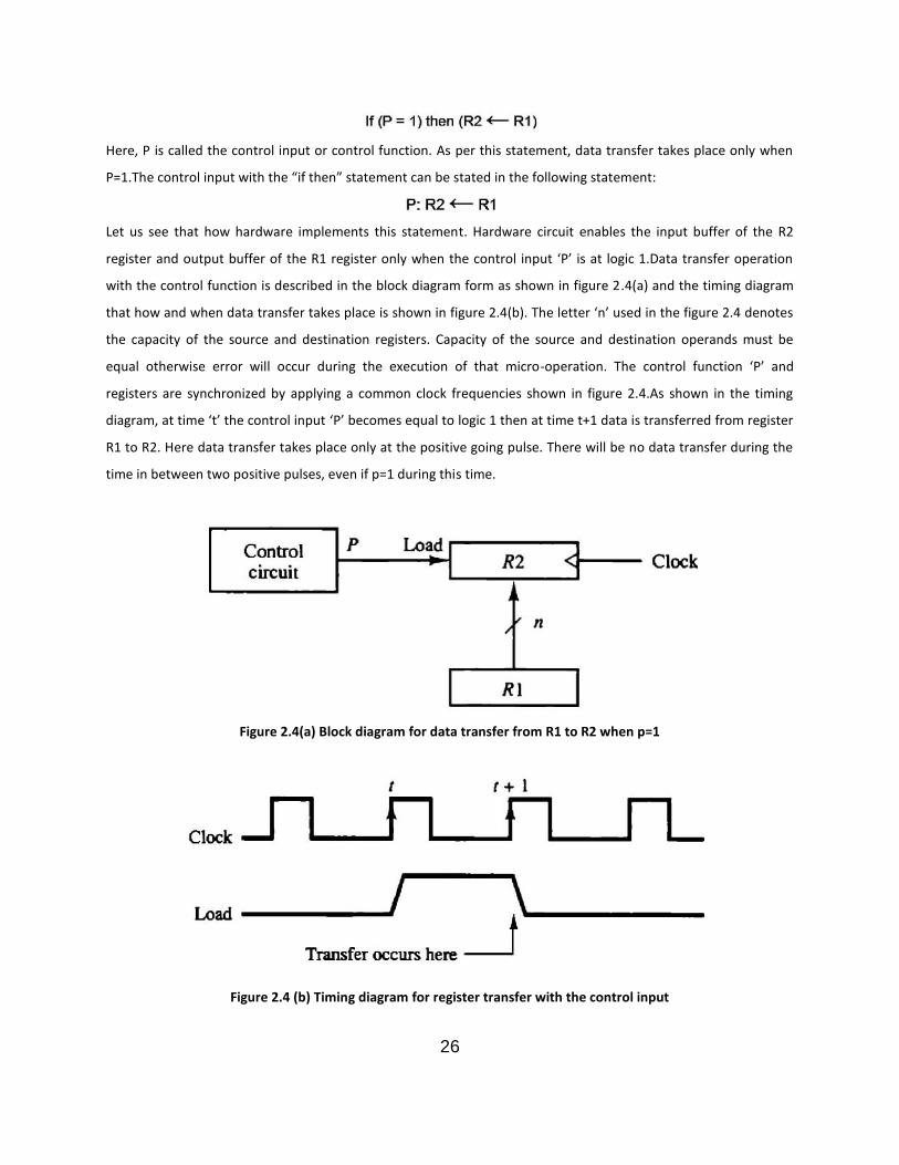
26
Here, P is called the control input or control function. As per this statement, data transfer takes place only when
P=1.The control input with the “if then” statement can be stated in the following statement:
Let us see that how hardware implements this statement. Hardware circuit enables the input buffer of the R2
register and output buffer of the R1 register only when the control input ‘P’ is at logic 1.Data transfer operation
with the control function is described in the block diagram form as shown in figure 2.4(a) and the timing diagram
that how and when data transfer takes place is shown in figure 2.4(b). The letter ‘n’ used in the figure 2.4 denotes
the capacity of the source and destination registers. Capacity of the source and destination operands must be
equal otherwise error will occur during the execution of that micro-operation. The control function ‘P’ and
registers are synchronized by applying a common clock frequencies shown in figure 2.4.As shown in the timing
diagram, at time ‘t’ the control input ‘P’ becomes equal to logic 1 then at time t+1 data is transferred from register
R1 to R2. Here data transfer takes place only at the positive going pulse. There will be no data transfer during the
time in between two positive pulses, even if p=1 during this time.
Figure 2.4(a) Block diagram for data transfer from R1 to R2 when p=1
Figure 2.4 (b) Timing diagram for register transfer with the control input
27
The symbolic notations of the basic register transfer are given in the table 2.1. Combination of capital letters and
numbers are used as the notations to represent various registers such as R1, R2 .... Rn.
Table 2.1 Basic symbols for register transfer operations
Sometimes only capital letters are used to name the registers. For example register A (Accumulator), B, SP (Stack
Pointer) etc. A sixteen bit registers can be subdivided into two eight bit registers and the part of the registers are
denoted by parentheses, for example PCL (D0 to D7) & PCH (D8-D15). The arrow shows the direction of the data flow
from the source operand to destination operand. To separate more than one
micro-operations comma is used in between the individual operation as shown in following statement.
The above operation shows two simultaneous register transfer operations i.e. when T=1 data of R2 is moved to R1
and at same time the data of R3 is transferred to register R2.
2.6 Bus System
The communication of data or signals in between various inbuilt modules of CPU (registers, memory, control unit
etc.) is possible through the bunch of wires called buses. There are different types of bus systems in the CPU such
as
Data Bus
Control Bus
Address Bus
Data bus is bidirectional and no of wires depends on the number of bits. The processor /CPU process of transfers
at a time. For example: 8 bit microprocessor has 8 data lines / buses. If individual busses are used for data flow in
between the registers then the bus system will be so cumbersome that it will be unable by the CPU to control it.
Thus for the communication in between various registers, memory or other units, a common bus system is used.

28
The common bus system is more efficient way for the communication in between various modules inside the CPU.
For data transfer there are two types of bus structures:
i. Internal bus structure, through which the devices/modules inside the CPU communicate
with each other.
ii. External bus system, the internal modules of the CPU communicates with the external
peripheral devices such as input devices, output devices, the external RAM or ROM.
A bus system consists of a number of common wires where one individual line/wire is used to transfer one bit of a
register and so on. There are different methods for designing the bus system. Simple and the efficient way for
designing the bus system is by using, either the multiplexer or the tri-state buffer.
2.6.1 Bus System Design Using Multiplexer
Multiplexers are one of the various logic devices used to design the common bus structure. Source register is
selected by the multiplexer for loading its data on to the bus. Design of common bus system for the data flow from
four registers is shown in the figure 2.5. Four bits of each register are numbered as 0(LSB) through 3(MSB).
Multiplexer with four inputs ad one output with two select lines S1 & S0(4×1 multiplexer) are used for the
selection of on register out of the 4 registers A,B,C,D of four bits each. As shown in figure 2.5, notations are used
for individual bits of each register (A3A2A1A0 for register A, B3B2B1B0 for register B and so on) for showing
connections of the bits through the bus lines with bit the multiplexer.
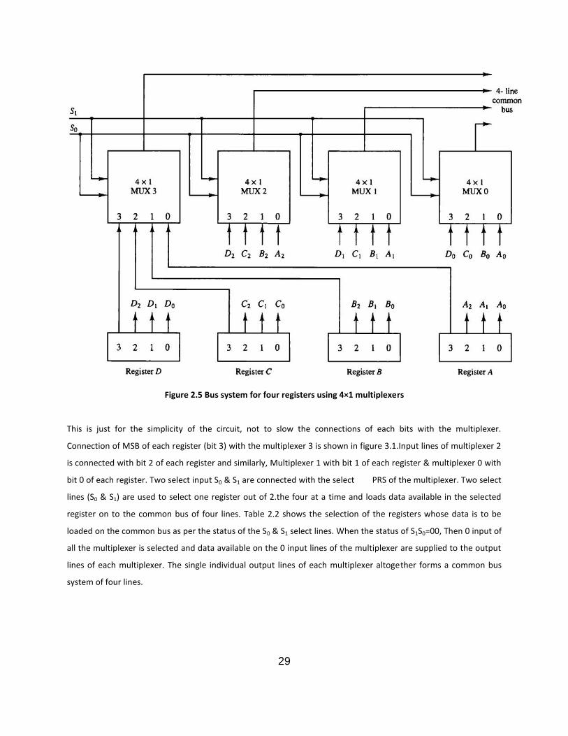
29
Figure 2.5 Bus system for four registers using 4×1 multiplexers
This is just for the simplicity of the circuit, not to slow the connections of each bits with the multiplexer.
Connection of MSB of each register (bit 3) with the multiplexer 3 is shown in figure 3.1.Input lines of multiplexer 2
is connected with bit 2 of each register and similarly, Multiplexer 1 with bit 1 of each register & multiplexer 0 with
bit 0 of each register. Two select input S0 & S1 are connected with the select PRS of the multiplexer. Two select
lines (S0 & S1) are used to select one register out of 2.the four at a time and loads data available in the selected
register on to the common bus of four lines. Table 2.2 shows the selection of the registers whose data is to be
loaded on the common bus as per the status of the S0 & S1 select lines. When the status of S1S0=00, Then 0 input of
all the multiplexer is selected and data available on the 0 input lines of the multiplexer are supplied to the output
lines of each multiplexer. The single individual output lines of each multiplexer altogether forms a common bus
system of four lines.
30
Table 2.2 Register selection as per status of status bits S1, S0 as in figure 2.5
Thus here when S1S0=01 transfers data of register B through this bus, S1S0=10 register C and so on. From above
discussion it is clear that to construct a 8 lines common bus system, 8 eight multiplexer of (8×1 multiplexer) with
three select lines, sixteen multiplexer(16×1 multiplexer) register with four select lines for the sixteen lines bus
structure & so no. The output lines of the multiplexer are connected with the input of destination register and
hence the data of source register which was loaded on the multiplexer output lines is transferred to the
destination register. Data transfer from one register through the bus can symbolically be represented by using the
word “BUS” in the statement as given below
As per this statement contents of register A is loaded to the bus and then through the bus, the contents (A) are
loaded to register R2. The transfer of data from C to R1 can be represented by the direct statement such as
During execution of this micro-operation same process of data transfer is followed as discussed in previous
statement.
2.6.2 Bus System Design Using Tri-State Buffers
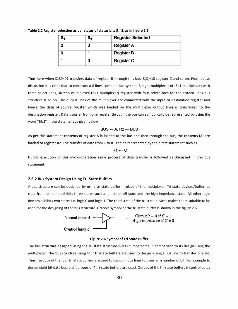
A bus structure can be designed by using tri-state buffer in place of the multiplexer. Tri-state devices/buffer, as
clear from its name exhibits three states such as on state, off state and the high impedance state. All other logic
devices exhibits two states i.e. logic 0 and logic 1. The third state of the tri-state devices makes them suitable to be
used for the designing of the bus structure. Graphic symbol of the tri-state buffer is shown in the figure 2.6.
Figure 2.6 Symbol of Tri State Buffer
The bus structure designed using the tri-state structure is less cumbersome in comparison to its design using the
multiplexer. The bus structure using four tri-state buffers are used to design a single bus line to transfer one bit.
Thus n groups of the four tri-state buffers are used to design n bus lines to transfer n number of bit. For example to
design eight bit data bus, eight groups of 4 tri-state buffers are used. Output of the tri-state buffers is controlled by

31
the control input ‘C’. The operation of tri-state buffer (shown in figure 2.6) as a function of the control input is
given in the table 2.2.
Table 2.3 Truth table of tri-state buffer
Operation of the tri state buffer is well understood from its truth table as shown in the table 2.3. When control
input “C” is equal to logic 1 then the buffer is said to be in active mode and its output will same as that of the
input. On other hand when control input “C” is at logic 0 then the buffer is inactive and is said to be in the high
impedance state. During high impedance state no current flows from input to the output side hence buffer is in the
off condition. The high impedance state is the special feature of the tri-state device. Here it must be noted that the
design of the common bus system is possible by using the tri-state device. Design of one line of the common bus
system using one set of the four buffers is shown in the figure 2.7. Least significant bit (D0C0B0A0) of the number is
connected at the input of the buffers and output of the buffers is tied together to form a single common bus to
transfer bit 0 or LSB of a number.
Figure 2.7 Circuit of bus line using the tri-state buffer
Control input of these four devices is connected to the output pins of a 2X4 decoder. The decoder having two input
lines, one enable pin and four output lines selects one buffer at a time out of the four shown in figure 2.7 as per
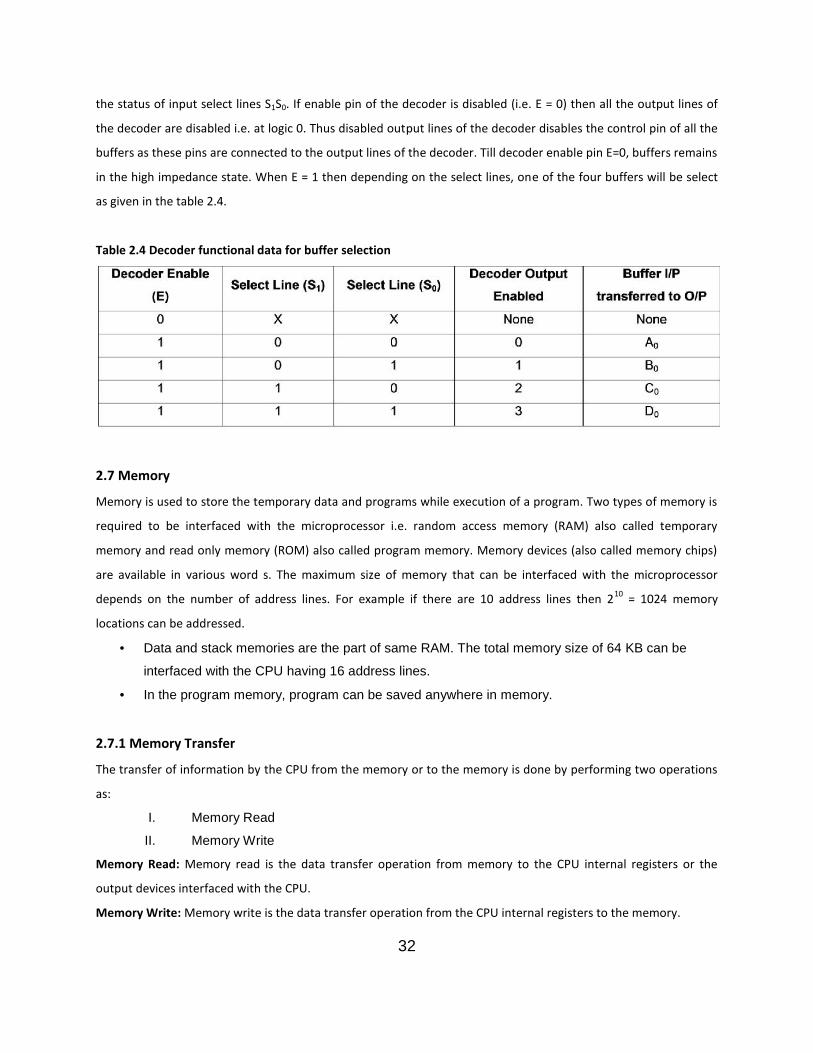
32
the status of input select lines S1S0. If enable pin of the decoder is disabled (i.e. E = 0) then all the output lines of
the decoder are disabled i.e. at logic 0. Thus disabled output lines of the decoder disables the control pin of all the
buffers as these pins are connected to the output lines of the decoder. Till decoder enable pin E=0, buffers remains
in the high impedance state. When E = 1 then depending on the select lines, one of the four buffers will be select
as given in the table 2.4.
Table 2.4 Decoder functional data for buffer selection
2.7 Memory
Memory is used to store the temporary data and programs while execution of a program. Two types of memory is
required to be interfaced with the microprocessor i.e. random access memory (RAM) also called temporary
memory and read only memory (ROM) also called program memory. Memory devices (also called memory chips)
are available in various word s. The maximum size of memory that can be interfaced with the microprocessor
depends on the number of address lines. For example if there are 10 address lines then 210 = 1024 memory
locations can be addressed.
Data and stack memories are the part of same RAM. The total memory size of 64 KB can be
interfaced with the CPU having 16 address lines.
In the program memory, program can be saved anywhere in memory.
2.7.1 Memory Transfer
The transfer of information by the CPU from the memory or to the memory is done by performing two operations
as:
I. Memory Read
II. Memory Write
Memory Read: Memory read is the data transfer operation from memory to the CPU internal registers or the
output devices interfaced with the CPU.
Memory Write: Memory write is the data transfer operation from the CPU internal registers to the memory.
33
For performing the data transfer operations, memory is denoted or symbolized by capital letter ‘M’. Address of the
memory location(s) is necessarily required to define in the micro-operation. The address of memory location to be
accessed is symbolized as [AR] i.e. address of the memory to be accessed is defined in the square bracket followed
by the letter ‘M’. The micro-operation used to read data from the memory is stated as follows:
In this micro-operation DR is called the data register and the address of memory location whose data is loaded into
the data register is represented by [AR]. The destination register for the memory read operation can be any of the
CPU internal registers such as registers A, B, C, H, L, R1 etc. Source memory location remains unchanged in the
memory read operation. Micro-operation used to write data to the memory from any of the available CPU
registers (R1 in the micro-operation) is stated as:
In this micro-operation contents of register R1 are written to the memory location pointed by the address This
causes a transfer of information from R1 into the memory word M selected by the bracketed address AR in this
case. Memory write operation does not change the contents of the source register.
2.8 Self Assessment Questions1. Data bus is........ .
a) uni-directional
b) bi-directional
c) tri-directional
d) none of these
2. Which one of the following statements, is memory read operation.
a. R1 ← M [AR]
b. M [AR] ← R2
c. R1 ← R2
d. None of the above
3. Read/write memory is.......
a) Volatile
b) non volatile
c) read only
d) none of these
4. Which one of the following is a Register transfer operation?
34
a) R3 ← R3-1
b) R1 ← R2+R3
c) R1 ← R2
d) All of the above
5. Buffer is a ________ state device.
a) 1
b) 2
c) 3
d) 4
6. Which of the register is connected to Memory Bus ?
a) PC
b) MAR
c) IR
d) All of these
2.9 Summary
Micro-operations can be performed by writing instructions/commands using symbols. Letters, Numbers, special
characters etc. are used as symbols to perform functions.. The method of performing the micro - operations by
writing symbols is easy to understand and reduces complexity of programming. Various operations covered in this
chapter are summarized as:
Symbols used to transfer data from one Register to another register is called register transfer
language.
During register transfer operation arrow head points the data transfer from source register to
destination register.
While register transfer operation data in source register remains unchanged.
With control function, register transfer takes place only when control condition is active.
Letters and numerals denote a register, Parentheses denotes a part of register and comma
separates two micro-operations.
Bunch of internal wires used to transfer the data from registers to registers or memory is called
bus system.
Bus system can be designed using multiplexers or tri (three) state buffers.
Data can be written to or read from memory by specifying its address in square brackets.
Data of memory remains unchanged during memory read operation.
35
2.10 Glossary
Micro-operation – Operation performed on data stored in one or more registers.
Register – 8/16 bit storage device designed using 8/16 flip flops.
Register Transfer – Transfer of data from one register to another.
Programming Language – Procedure for performing operations (Arithmetic, Logic, etc..) by writing symbols.
M[AR] – Memory Address Register
Flip Flop – Basic memory element to store 1 bit
Memory – Group of Flip flops to store binary data
RAM – Random Access Memory
ROM – Read Only Memory
Memory Read – Transfer of data from memory to other devices (registers).
Memory Write – Transfer of data from other devices (registers) to memory.
BIT – A binary digit, 0 or 1
Byte – A group of eight bits
Nibble – A group of four bits
PC (L) – Program counter lower byte
PC (H) – Program counter higher byte
IR – Instruction register
M [0-7]- Lower byte of memory address
M (8-15) – Higher order memory address
Buffer – A logic circuit that amplifies current or power
High Impedance State – Buffer behaves as open circuit
2.11 Answers of Self Assessment QuestionsSection (2.1 to 2.3)
1. Micro – operation
2. Instruction Register
3. Program Counter
4. It is a system to perform sequence of micro – operations in symbolic form.
5. d
Section (2.4 to 2.5)
1. b
36
2. a
3. a
4. c
5. c
6. b
2.12 References/Bibliography/Suggested Readings
1. Computer System Architecture by M. Morris Mano, Pearson Publication.
2. Computer Architecture and Organization by J.P. Hays, Tata McGraw-Hill Publishing.
3. Computer Architecture: A Quantitative Approach. J. L. Hennessy and D. A. Patterson Morgan Kaufmann,
San Francisco, CA, fifth edition
4. Computer Organization and Architecture by William Stallings, Pearson Publication
5. Computer Organization and Design, Pal Choudhary, PHI
6. www.nptel.iitm.ac.in
2.13 Terminal and Model Questions
1. What are the register transfer instructions?
2. What do you mean by direct and indirect addressing?
3. Explain the concept and structure of common bus system.
4. What is the function registers? Explain various registers of computer organization.
5. Show the block diagram of the hardware that implements the following register transfer statement:
T : R2 ← R1, RI ← R2
6. Represent the following conditional control statement by two register transfer statements with control
functions.
If (P = 1) then (Rl ← R2) else if (Q = 1) then (Rl ← R3)
7. Explain the memory operation in each of the following data transfer statements:
a. R2←M[AR]
b. M[AR] ← R3
c. R5 ← M[R5]
37
Lesson 3
Micro - operations
Structure
3.0 Objectives
3.1 Introduction
3.2 Types of Micro-operations
3.3 Arithmetic and Shift Operations
3.3.1 Hardware Implementation of Arithmetic Micro – operations
3.3.1.1 Binary Adder
3.3.1.2 Binary Adder-Subtractor
3.3.1.3 Binary Incrementer
3.4 Self Assessment Questions (Section 3.1 to 3.3)
3.5 Logic Micro-operations
3.5.1 List of Logic Micro – operations
3.5.2 Hardware Implementation for Logic Operations
3.6 Shift Micro - Operations
3.6.1 Logical Shift
3.6.2 Circular Shift
3.6.3 Arithmetic Shift
3.6.4 Hardware Implementation of Shift Operations
3.7 Self Assessment Questions (Section 3.5 to 3.6)
3.8 Summary
3.9 Glossary
3.10 Answers to Check Your Progress/ Self Assessment Questions (SAQ)
3.11 Bibliography/References/Suggested Readings
3.12 Terminal and Model Questions
3.0 Objectives
To understand concept of arithmetic, Logic and shift operations.
Study micro-operations to perform arithmetic, Logic and shift operations.
38
Symbolic instruction format.
Hardware design for the arithmetic, Logic and shift operations.
After the completion of this chapter students will be able to understand the basic concepts of arithmetic, Logic and
shift micro-operations and the set of symbols/special characters to perform these micro-operations. This will help
them to proceed for the skill development to write the sequence of instructions in symbolic form to perform
various micro-operations and hardware design for the same.
3.1 Introduction
Computers are designed by the integrated combination of hardware and software. Internal architecture of CPU
which contains digital logic circuits, registers to store data etc. The software is the sequence of operations
performed on data stored in registers and is called as micro-operations. The result obtained after the operation is
performed, may replace the already stored binary data of a register or may be saved to another register. Examples
of micro-operations are compliment, addition, increment, subtraction, decrement, shift, count, clear etc. ALU is
responsible to perform the operation in the computer. The basic operations are implemented by hardware.
3.2 Types of Micro-operations
The micro-operations most often encountered in digital computers are classified into four categories:
1. Arithmetic micro-operations perform increment, decrement, addition, subtraction etc. Arithmetic
operations on binary data stored in internal registers.
2. Logic micro-operations perform compliment, OR, XOR, AND, NAND, Compare etc. Micro
operations on binary data stored in memory or internal register.
3. Shift micro-operations perform data shift operations as shift right, left, circular shift etc. on binary
data stored in internal registers.
4. Registers transfer micro-operations (already discussed) moves binary data from one register to
memory or another register.
Register transfer micro-operations are already discussed in chapter 2. These micro-operation are used in
conjunction with other three types of micro-operations.
3.3 Arithmetic Micro-operations
Various arithmetic micro-operations performed on data in registers or memory are add, increment, subtract,
decrement. Arithmetic micro-operations can be expressed by the statements:

39
Above statements defines an addition and subtraction micro-operation. In the 1st statement, the data of register
R1 is added to the data of register R2 and the result after this operation is saved to register RA. To perform
operations as per above statements with the hardware, we need 3 registers and the digital logic component. The
various other arithmetic micro operations are listed in Table 3.1. There is no separate logic circuit to perform the
subtraction; hence subtraction is most often implemented through 2’s compliment method and addition. In 2’s
compliment method, Instead of using the minus symbol, the subtraction can be expressed (using 2’s compliment
method) by the following micro - operation:
Bar on the register R2 i.e., ( 2) represents the 1's complement of register R2. Addition of one to the 1's
complement of R2, converts data in it to the 2's complement form. Addition of the contents of register R1 to the
2's complemented contents of R2 is similar to the direct subtraction micro-operation R1 - R2.
Table 3.1 Arithmetic Micro - operations
The decrement and increment micro-operations are represented by -1 and +1 statements,
respectively.
These micro-operations are implemented with a digital logic circuit or with up-down counter.
The micro-operations for multiplication and division of numbers are not given in Table 3.1. These
two micro-operations are valid arithmetic operations but most of the times, are not part of the
basic set of micro-operations.

40
The only area, where these micro-operations are considered as micro-operations is in the digital
system, where they are implemented by using digital combinational circuits.
The arithmetic micro-operations are performed through the logic circuits which are basically
combination of logic gates, and the result of operations is saved to the register designated as
destination register.
In most of the systems, the multiplication micro - operation is implemented with the successive
addition and shift micro-operations.
On other hand, the division micro - operation is implemented with the successive subtraction and
shift micro-operations.
To implement these operations by the digital hardware, a list of micro-operations that use the
basic operations of addition, subtraction and shift are described.
3.3.1 Hardware Implementation of Arithmetic Micro - operations
To perform operation of addition micro-operation with digital hardware circuits, we require the registers that store
the numbers and the combination of logic components that performs this arithmetic addition. Micro-operations
are implemented using digital components like multiplexers, logic gates, decoders, system bus, full adders etc. The
digital circuit that generates the arithmetic sum of 2 binary bits along with carry (if any) is called a binary full adder
circuit.
3.3.1.1 Binary Adder
A digital circuit that calculates the sum of 2 binary numbers (along with carry) of any lengths is called a digital
binary adder. The binary adder is designed by using full adder (FA) logic circuits connected in cascaded form. In the
cascaded logic circuit connections, the output carry of first full adder is applied to the input carry connection of the
next full-adder and so on.
Figure 3.1 Hardware of 4 bit binary adder
41
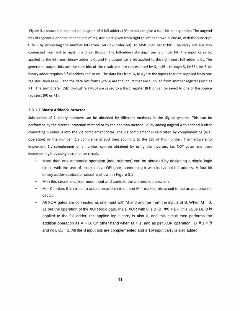
Figure 3.1 shows the connection diagram of 4 full adders (FA) circuits to give a four-bit binary adder. The augend
bits of register A and the addend bits of register B are given from right to left as shown in circuit, with the subscript
0 to 3 by expressing the number bits from LSB (low-order bit) to MSB (high order bit). The carry bits are also
connected from left to right in a chain through the full-adders starting from left most FA. The input carry bit
applied to the left most binary adder is C0 and the output carry bit applied to the right most full adder is C4. The
generated output bits are the sum bits of the result and are represented by S0 (LSB ) through S3 (MSB). An 8-bit
binary adder requires 8 full-adders and so on. The data bits from A0 to A3 are the inputs that are supplied from one
register (such as R0), and the data bits from B0 to B3 are the inputs that are supplied from another register (such as
R1). The sum bits S0 (LSB) through S3 (MSB) are saved to a third register (R3) or can be saved to one of the source
registers (R0 or R1).
3.3.1.2 Binary Adder-Subtractor
Subtraction of 2 binary numbers can be obtained by different methods in the digital systems. This can be
performed by the direct subtraction method or by the addition method i.e. by adding augend A to addend B after
converting number B into the 2's complement form. The 2's complement is calculated by complimenting (NOT
operation) by the number (1's complement) and then adding 1 to the LSB of this number. The hardware to
implement 1's complement of a number can be obtained by using the inverters i.e. NOT gates and then
incrementing it by using incrementer circuit.
More than one arithmetic operation (add, subtract) can be obtained by designing a single logic
circuit with the use of an exclusive-OR gate, connecting it with individual full adders. A four-bit
binary adder-subtractor circuit is shown in Figure 3.2.
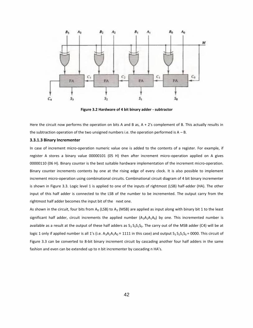
M in this circuit is called mode input and controls the arithmetic operation.
M = 0 makes this circuit to act as an adder circuit and M = makes this circuit to act as a subtractor
circuit.
All XOR gates are connected as one input with M and another from the inputs of B. When M = 0,
as per the operation of the XOR logic gate, the B XOR with 0 is B (B 0 = B). This value i.e. B is
applied to the full adder, the applied input carry is also 0, and this circuit then performs the
addition operation as A + B. On other hand when M = 1, and as per XOR operation, B 1 =
and now C0 = 1. All the B input bits are complemented and a 1of input carry is also added.
42
Figure 3.2 Hardware of 4 bit binary adder - subtractor
Here the circuit now performs the operation on bits A and B as, A + 2's complement of B. This actually results in
the subtraction operation of the two unsigned numbers i.e. the operation performed is A – B.
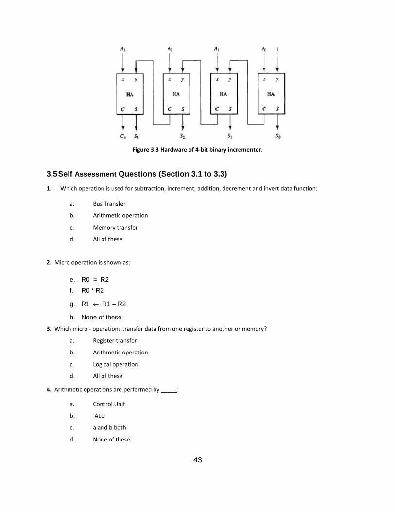
3.3.1.3 Binary Incrementer
In case of increment micro-operation numeric value one is added to the contents of a register. For example, if
register A stores a binary value 00000101 (05 H) then after increment micro-operation applied on A gives
00000110 (06 H). Binary counter is the best suitable hardware implementation of the increment micro-operation.
Binary counter increments contents by one at the rising edge of every clock. It is also possible to implement
increment micro-operation using combinational circuits. Combinational circuit diagram of 4 bit binary incrementer
is shown in Figure 3.3. Logic level 1 is applied to one of the inputs of rightmost (LSB) half-adder (HA). The other
input of this half adder is connected to the LSB of the number to be incremented. The output carry from the
rightmost half adder becomes the input bit of the next one.
As shown in the circuit, four bits from A0 (LSB) to A3 (MSB) are applied as input along with binary bit 1 to the least
significant half adder, circuit increments the applied number (A3A2A1A0) by one. This incremented number is
available as a result at the output of these half adders as S3 S2S1S0. The carry out of the MSB adder (C4) will be at
logic 1 only if applied number is all 1’s (i.e. A3A2A1A0 = 1111 in this case) and output S3 S2S1S0 = 0000. This circuit of
Figure 3.3 can be converted to 8-bit binary increment circuit by cascading another four half adders in the same
fashion and even can be extended up to n bit incrementer by cascading n HA’s.
43
Figure 3.3 Hardware of 4-bit binary incrementer.
3.5Self Assessment Questions (Section 3.1 to 3.3)
1. Which operation is used for subtraction, increment, addition, decrement and invert data function:
a. Bus Transfer
b. Arithmetic operation
c. Memory transfer
d. All of these
2. Micro operation is shown as:
e. R0 = R2
f. R0 * R2
g. R1 ← R1 – R2
h. None of these
3. Which micro - operations transfer data from one register to another or memory?
a. Register transfer
b. Arithmetic operation
c. Logical operation
d. All of these
4. Arithmetic operations are performed by _____:
a. Control Unit
b. ALU
c. a and b both
d. None of these
44
5. Which of the following micro-operation performs 2’s compliment?
a. R3 ← R1 + R2
b. R2 ← R2c. R1 ← R1 + 1
d. R2 ← R2 + 1
6. R3 ← R1 + R2 + 1; performs subtraction micro-operation. True/False
7. In the logic circuits, subtraction of two numbers is performed by
a. 9’s complement
b. 10’s complement
c. 1’s complement
d. 2’s complement
3.5 Logic Micro-operations
Logical micro-operations are performed on the data saved in the internal registers or memory. Various logic
functions such as AND, OR, NOT, XOR, NAND, NOR, Compare etc. are performed on the individual bits stored in the
registers. Following is the example, of XOR (exclusive-OR) micro-operation performed on data in the registers R0
and R3:
This micro-operation performs XOR operation on the bits at individual (one by one) basis with the condition that
control variable P is at logic 1. Here assume that register R0 contains 0011 and register R3 contains 0101 as four bit
registers. The XOR micro-operation given above is computed as follows:
0011; Content of R1
0101; Content of R2____
0110; Content of R1 after P = 1
Four 2 input XOR gates are used in which Data of register R0 is 1st input and data in register R3
is the 2nd input of this gate.
Execution of above micro-operation gives result which is a four bit binary number 0110 saved in
the register R0 after the operation is over. Basically this micro-operation is used to compare two
data as we know that output of XOR gate is high only when logic level of both inputs is different.
To perform AND, complement and OR logic operations, special characters are used to write
these micro-operations.
“V” symbol is used to represent or specify an OR micro-operation.
“ᴧ” symbol is used to represent or specify an AND micro-operation.

45
A bar on top of the register is used to represent the complement micro-operations.
The use of different symbols differentiates a logic micro-operations and a control (or Boolean)
variable.
These special characters also differentiates the symbol + that represents arithmetic addition as
compared to logic OR operation.
For writing micro-operation, + symbol is never used to denote an OR micro-operations.
For example, as differentiated in the following micro-operation:
In this micro-operation, the + symbol in between A and B is representing an OR operation between two binary
variables of a control function. The + between R0 and R3 specifies an add micro-operations The OR micro-
operations is represented by the symbol “V” in between registers R5 and R6.
3.5.1 List of Logic Micro - operations
There are about 16 logic operations which are derived by using 2 binary variables x and y to perform these sixteen
logic micro-operation. These operations can be obtained from all possible combinations of the two variables x and
y. Different combinations are shown in the table 3.2 in the form of truth table. Sixteen columns F0 to F15 as shown
in the truth table, shows one of the possible Boolean function for the given two variables x and y. Here sixteen
binary combinations (F0 to F15) as given in the table give different logic operations correspondingly. These logic
operations (expressed by 2 variables x and y) in the Boolean and micro-operation form are as given in the table
3.3.
Table 3.2 Truth Tables for sixteen Functions of Two Variables

46
Table 3.3 Sixteen Logic Micro – operations
In the table 3.3, column 1 names the micro-operation, column two defines the logic variables x, y and represents
the logic operation to be performed by the logic micro-operation given in the column three. Column four explains
each micro-operation performed on the registers in detail for better understanding of these micro-operations.
Here it is worth noting that logic micro-operations are performed on the individual bits of the registers i.e. bit D0
register R1 (2nd operation as per table) is logically Anded with the D0 bit of register R2 and this process is carried
out till MSB of both the registers are logically Anded and result is available at the ( F )output.
3.5.2 Hardware Implementation for Logic Operations
Logic gates are the backbone for hardware circuits design to implement various logic micro-operations to perform
logic operations on the individual bits stored in the registers. As per the table 3.3 we have studied sixteen logic
micro-operations and all these can be implemented using digital hardware components. But most of the systems

47
design hardware circuits to implement four basic micro-operations such as logical OR, XOR, Complement (NOT)
and AND. All other left out micro-operations can be implemented by using these four basic operations. Hardware
implementation of these four micro-operations is shown in the figure 3.4. A multiplexer (4 × 1) and four basic logic
gates are used in this circuit. Each logic gate is dedicated to perform an individual operation. Out of these four only
one gate is selected to perform its logic operation depending upon the logic level of the select lines S0 and S1.
Output of the selected gate is then available at the output line of the multiplexer.

48
Figure 3.4 Circuit diagram for implementation of four logic operations
Four micro-operations implemented in the hardware circuit as shown in figure 3.4 are described in the function
table 3.4. From this table it is very clear that logics of S1 S0 decides, which of the available four micro-operations
will be selected.
Table 3.4 Function Table to implement four logic operations
3.6 Shift Micro - Operations
49
Shift micro - operations are used to shift bits position in a register to the left or the right side. These micro-
operations are sometimes used along with other type of micro-operations such as data transfer, arithmetic or
logic. To perform shift operations different types of shift registers are used, which are further designed using basic
flip flops.
When each Bit is transferred to the left side by one bit position and MSB is transferred to the LSB,
then this is called shift left micro-operation.
When each Bit is transferred to the right side by one bit position and LSB is transferred to the
MSB, then this is called shift right micro-operation.
Depending on the nature of data shifted, the Shift micro – operations are further divided in the
three categories as: logical shift, arithmetic shift and circular.
3.6.1 Logical Shift
In this type of shift micro - operation bits position in a register is shifted to the left side and after the shift
operation shifted data is retained in the same register. As shown in the examples below, ‘shr’ and ‘shl’ are used as
symbols to shift bits right and left respectively. Examples of logical shift micro-operations are given as follows:
In the first micro-operation bits of register R1 are shifted to the left side by one bit position and result after the
shift operation is retained in the register R1 itself. Same process is followed in the 2nd operation except that shift of
bits is towards right side. It is to note here that during logical shift left MSB is lost and during logical shift right LSB
is lost.
3.6.2 Circular Shift
The circular shift is similar to logical shift but here bits are not lost.
It is also called rotate micro-operation because during circular left shift of the bits MSB shifts to
the position of LSB. Hence no loss of MSB in this shift.
Serial Input Serial Output (SISO) shift register is used to implement the circular shift operations.
“cil” is used as a symbol to represent the circular shift left micro-operation.
“cir” is used as a symbol to represent the circular shift right micro-operation.
Various symbols used for the shift micro - operations are listed in the Table 3.5.
Table 3.5 Shift Micro – operations
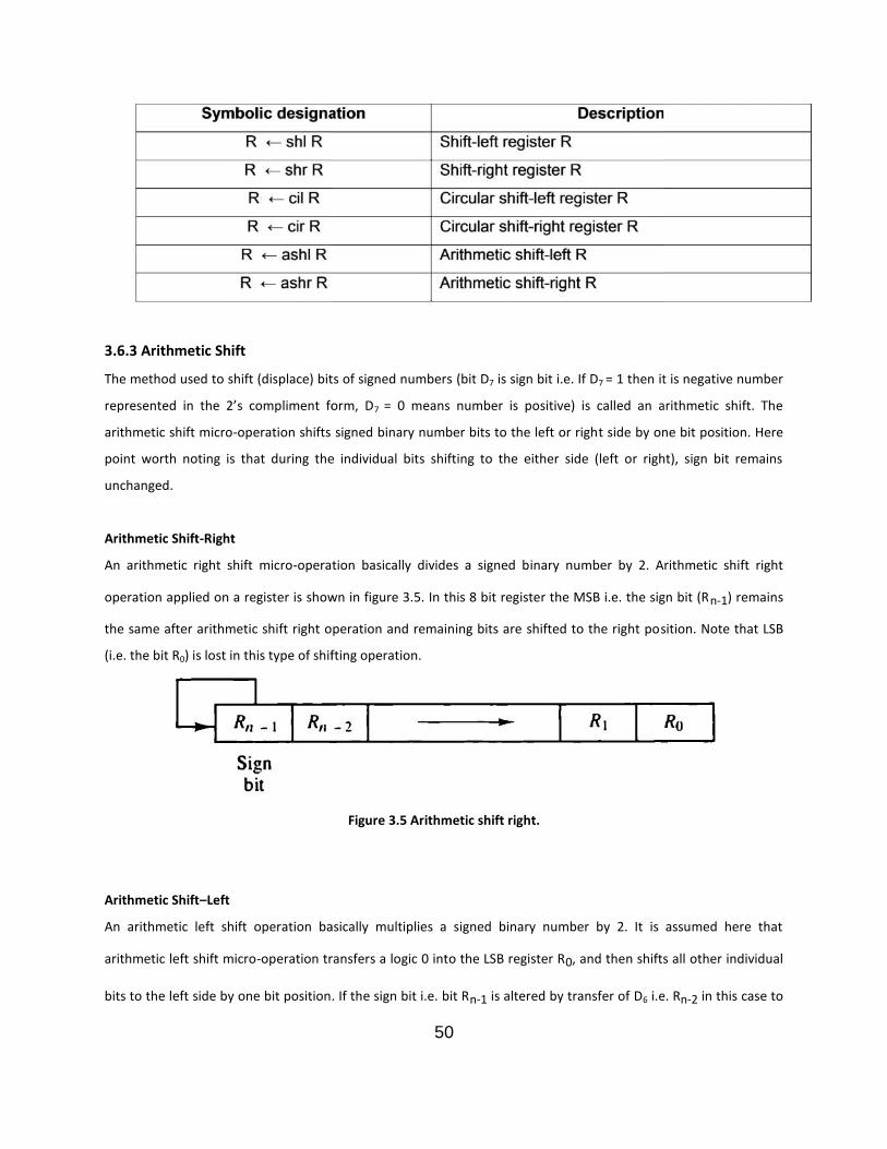
50
3.6.3 Arithmetic Shift
The method used to shift (displace) bits of signed numbers (bit D7 is sign bit i.e. If D7 = 1 then it is negative number
represented in the 2’s compliment form, D7 = 0 means number is positive) is called an arithmetic shift. The
arithmetic shift micro-operation shifts signed binary number bits to the left or right side by one bit position. Here
point worth noting is that during the individual bits shifting to the either side (left or right), sign bit remains
unchanged.
Arithmetic Shift-Right
An arithmetic right shift micro-operation basically divides a signed binary number by 2. Arithmetic shift right
operation applied on a register is shown in figure 3.5. In this 8 bit register the MSB i.e. the sign bit (Rn-1) remains
the same after arithmetic shift right operation and remaining bits are shifted to the right position. Note that LSB
(i.e. the bit R0) is lost in this type of shifting operation.
Figure 3.5 Arithmetic shift right.
Arithmetic Shift–Left
An arithmetic left shift operation basically multiplies a signed binary number by 2. It is assumed here that
arithmetic left shift micro-operation transfers a logic 0 into the LSB register R0, and then shifts all other individual
bits to the left side by one bit position. If the sign bit i.e. bit Rn-1 is altered by transfer of D6 i.e. Rn-2 in this case to
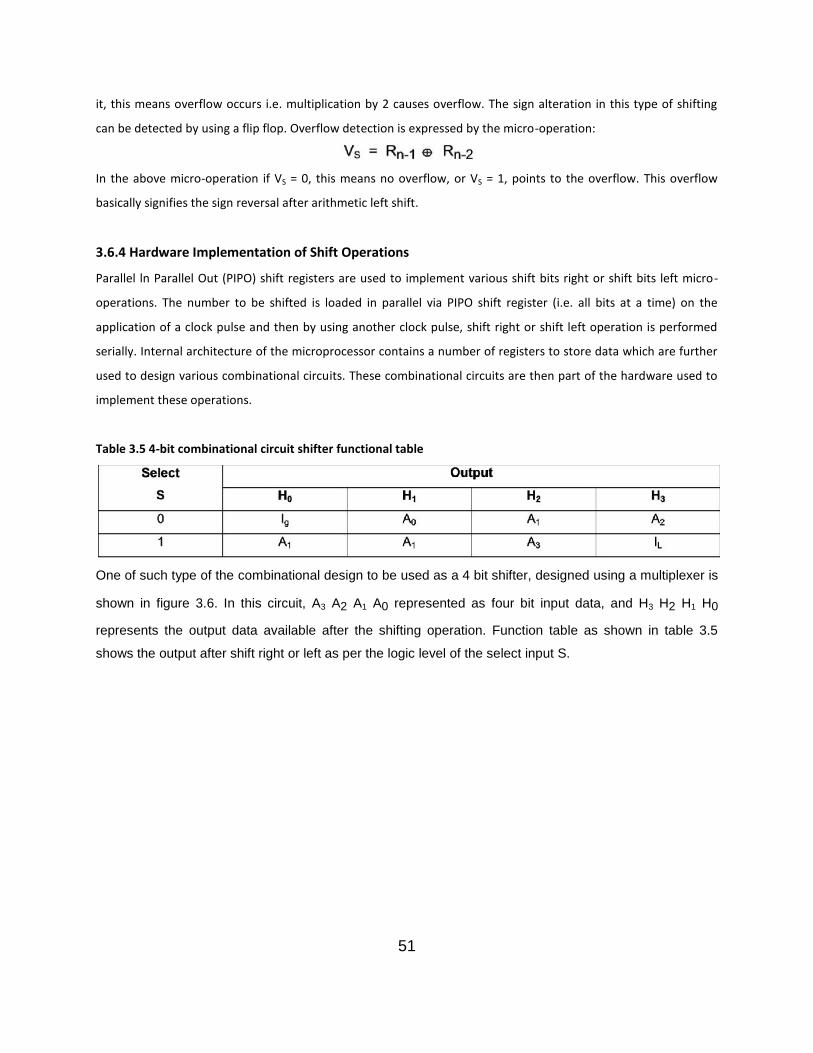
51
it, this means overflow occurs i.e. multiplication by 2 causes overflow. The sign alteration in this type of shifting
can be detected by using a flip flop. Overflow detection is expressed by the micro-operation:
In the above micro-operation if VS = 0, this means no overflow, or VS = 1, points to the overflow. This overflow
basically signifies the sign reversal after arithmetic left shift.
3.6.4 Hardware Implementation of Shift Operations
Parallel ln Parallel Out (PIPO) shift registers are used to implement various shift bits right or shift bits left micro-
operations. The number to be shifted is loaded in parallel via PIPO shift register (i.e. all bits at a time) on the
application of a clock pulse and then by using another clock pulse, shift right or shift left operation is performed
serially. Internal architecture of the microprocessor contains a number of registers to store data which are further
used to design various combinational circuits. These combinational circuits are then part of the hardware used to
implement these operations.
Table 3.5 4-bit combinational circuit shifter functional table
One of such type of the combinational design to be used as a 4 bit shifter, designed using a multiplexer is
shown in figure 3.6. In this circuit, A3 A2 A1 A0 represented as four bit input data, and H3 H2 H1 H0
represents the output data available after the shifting operation. Function table as shown in table 3.5
shows the output after shift right or left as per the logic level of the select input S.

52
Figure 3.6 4-bit combinational circuit shifter
Control input S is used to operate this circuit for either shift right or for the shift left operation as per the
following logic:
S = 1; The circuit (Figure 3.6) acts as a left shifter,
S = 0; The circuit (Figure 3.6) acts as a right shifter.
Serial input for shift left is IL Serial input for shift right is IR.
3.7 Self Assessment Questions (Section 3.5 to 3.6)
1. F ← 1 ᴧ 2 is........ . type of micro-operation.
a) Arithmetic
b) Logic
c) Shift

53
d) None of these
2. Logic exclusive OR (XOR) operation of 1st number (0100101011000000) B with 2nd number (1011010100111111)
B results
a. 1010101011001011 B
b. 0000000000000000 B
c. 1111111111111111 B
d. 0100101011000000 B
3. A two input NOR gate will have output at logic 1 only when
a. one of the two inputs is high
b. Both inputs are low
c. Both inputs are high
d. All of above
4. The 2’s compliment of an eight bit number 00001010 B is
a. 11110110 B
b. 00001111 B
c. 11111010 B
d. 00001010 B
5. A combinational circuit designed to shift a binary number bits to the right or the left position is called a
a. Program counter
b. Shift register
c. Serial register
d. Parallel register
6. The micro-operation: R
a. Shift bits of register R to right position
b. Circulate bits of register R to right position
c. Arithmetic Shift-right bits of register R
d. All of above
7. Which of the following performs NAND operation?
a. F ← 1 V 2b. F ← 1c. F ← 1 V 2d. F ← 1 ᴧ 2
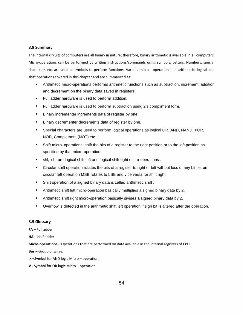
54
3.8 Summary
The internal circuits of computers are all binary in nature; therefore, binary arithmetic is available in all computers.
Micro-operations can be performed by writing instructions/commands using symbols. Letters, Numbers, special
characters etc. are used as symbols to perform functions. Various micro - operations i.e. arithmetic, logical and
shift operations covered in this chapter and are summarized as:
Arithmetic micro-operations performs arithmetic functions such as subtraction, increment, addition
and decrement on the binary data saved in registers.
Full adder hardware is used to perform addition.
Full adder hardware is used to perform subtraction using 2’s compliment form.
Binary incrementer increments data of register by one.
Binary decrementer decrements data of register by one.
Special characters are used to perform logical operations as logical OR, AND, NAND, XOR,
NOR, Complement (NOT) etc.
Shift micro–operations; shift the bits of a register to the right position or to the left position as
specified by that micro-operation.
shl, shr are logical shift left and logical shift right micro-operations .
Circular shift operation rotates the bits of a register to right or left without loss of any bit i.e. on
circular left operation MSB rotates to LSB and vice versa for shift right.
Shift operation of a signed binary data is called arithmetic shift .
Arithmetic shift left micro-operation basically multiplies a signed binary data by 2.
Arithmetic shift right micro-operation basically divides a signed binary data by 2.
Overflow is detected in the arithmetic shift left operation if sign bit is altered after the operation.
3.9 Glossary
FA – Full adder
HA – Half adder
Micro-operations – Operations that are performed on data available in the internal registers of CPU.
Bus – Group of wires.
ᴧ –Symbol for AND logic Micro – operation.
V - Symbol for OR logic Micro – operation.
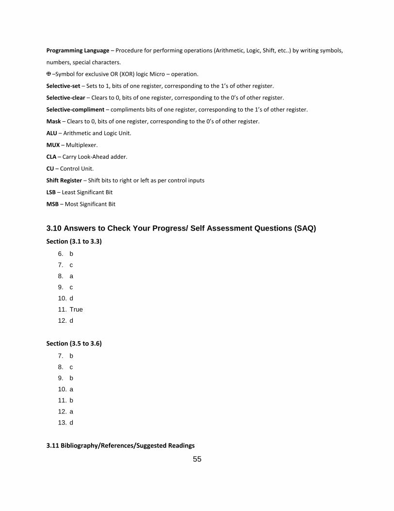
55
Programming Language – Procedure for performing operations (Arithmetic, Logic, Shift, etc..) by writing symbols,
numbers, special characters.
–Symbol for exclusive OR (XOR) logic Micro – operation.
Selective-set – Sets to 1, bits of one register, corresponding to the 1’s of other register.
Selective-clear – Clears to 0, bits of one register, corresponding to the 0’s of other register.
Selective-compliment – compliments bits of one register, corresponding to the 1’s of other register.
Mask – Clears to 0, bits of one register, corresponding to the 0’s of other register.
ALU – Arithmetic and Logic Unit.
MUX – Multiplexer.
CLA – Carry Look-Ahead adder.
CU – Control Unit.
Shift Register – Shift bits to right or left as per control inputs
LSB – Least Significant Bit
MSB – Most Significant Bit
3.10 Answers to Check Your Progress/ Self Assessment Questions (SAQ)Section (3.1 to 3.3)
6. b
7. c
8. a
9. c
10. d
11. True
12. d
Section (3.5 to 3.6)
7. b
8. c
9. b
10. a
11. b
12. a
13. d
3.11 Bibliography/References/Suggested Readings
56
7. “Computer System Architecture” by M. Morris Mano, Pearson Publication.
8. “Computer Architecture and Organization” by J.P. Hays, Tata McGraw-Hill Publishing.
9. “Computer Architecture: A Quantitative Approach” J. L. Hennessy and D. A. Patterson Morgan Kaufmann,
San Francisco, CA, fifth edition
10. “Computer Organization and Architecture” by William Stallings, Pearson Publication
11. “Computer Organization and Design”, Pal Choudhary, PHI
12. www.nptel.iitm.ac.in
3.12 Terminal and Model Questions
1. Register B holds the 8 bit binary 01011001. Write the logic micro operation to perform:
i. 2’s compliment and save result in register B
ii. 1’s compliment and save result in register A
iii. XOR with binary data 01111000 and save result in R1
iv. AND with register R2 and sane result in R2
2. An 8-bit register contains binary value 11011011. What will be its value after a circular shift right?
3. Design a 4-bit decrementer (combinational logic circuit) using four full adders (FA).
4. Design a logic circuit that performs any of the sixteen logic functions listed in Table 3.3.
5. The 8-bit registers A, B, C, and D initially has the following values:
A = 11010010
B = 10111111
C = 10101001
D = 11101011
Give the value of eight bit data available in each register as given above after the execution of the following
different micro-operations.
C ← C Ʌ D, B ← B + 1 logically AND register D to C, increment register B
A ← A + B Add B to A
A ← A - C Subtract data of register C from register A
6. Binary value 10110101 is saved in an eight bit register. What will be the value of this register after an arithmetic
shift right operation? Starting from the initial number 10110101, determine the register value after an arithmetic
shift left operation, and check whether there is an overflow of sign bit or not.
7. Determine the binary bits sequence of data stored in a register R1 = 01110001after a circular shift-right, logical
shift-left, followed by a circular shift-left and logical shift-right.
8. Show the contents of output (H) in Figure 3.6 if input A is 1011, S = 0, IR = 0, and IL = 1?

57
9. A register stores an eight bit binary 11011001. Which logic micro-operation is to be performed in order to
convert the data in register A to the following data?
a. 01101101
b. 11111101
10. Design a digital system that performs the four logic operations such as XOR, XNOR, NOR, and NAND. Use two
selection inputs. Also Show the logic diagram for at least one stage.
58
Lesson 4
Common Bus System
Structure
4.0 Objectives
4.1 Introduction
4.2 Common Bus System
4.3 Types of Buses
4.3.1 Address Bus
4.3.2 Data Bus
4.3.3 Control Bus
4.3.4 Complications in Single Bus System
4.4 Data movement among Registers using Common Bus
4.5 Summary
4.6 Glossary
4.7 Answers to Check Your Progress/Suggested Answers to SAQ
4.8 Terminal and Model Questions
4.0 Objectives
The main objective of this chapter is to make students understand:
What is a common bus and why we use it in computer architecture?
Various types of registers and there connection using bus
Types of buses- address bus, data bus and control bus
How data is transferred between various registers and memory?
4.1 Introduction
This chapter aims at providing knowledge to the readers about the common bus system in basic computerorganization. It is the set of wires that provide a communication link between various devices. There are threetypes of buses used in the system - Address bus, Data bus and Control bus. The implementation of bus system willbe studied in detail. The bus is used for transferring the data among the registers and also among the register andthe memory unit. We will study how this data movement occurs among registers by using 16-bit common bus.
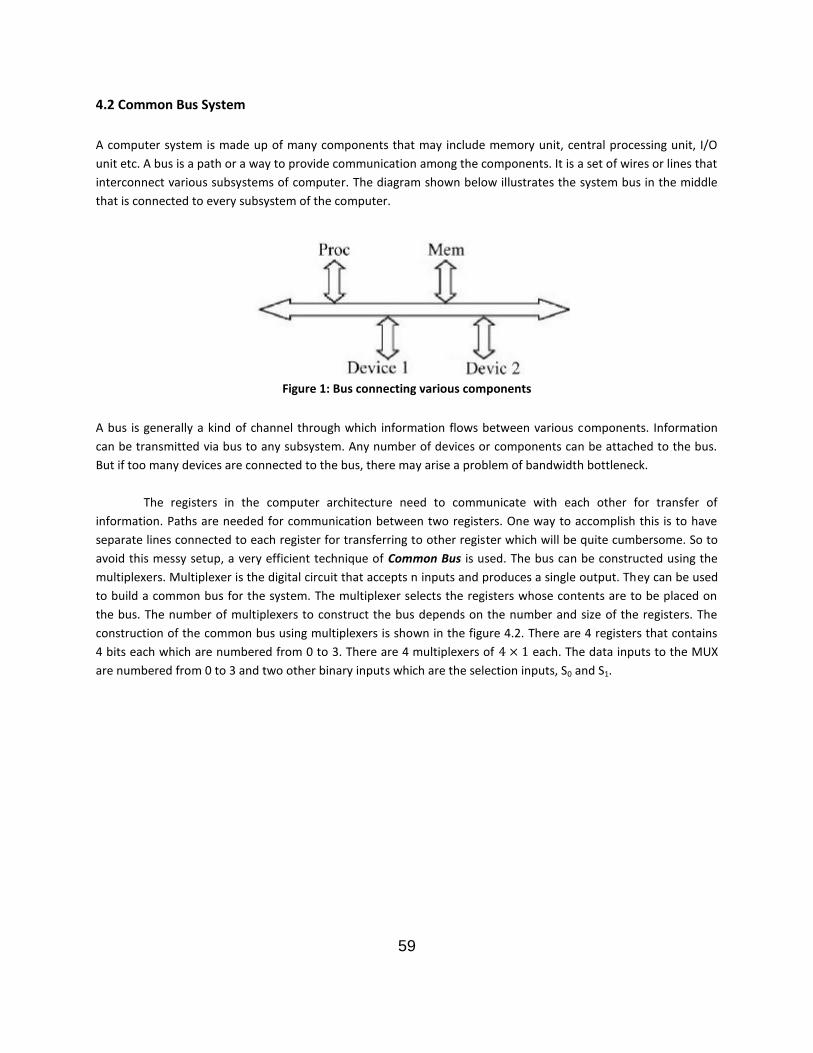
59
4.2 Common Bus System
A computer system is made up of many components that may include memory unit, central processing unit, I/Ounit etc. A bus is a path or a way to provide communication among the components. It is a set of wires or lines thatinterconnect various subsystems of computer. The diagram shown below illustrates the system bus in the middlethat is connected to every subsystem of the computer.
Figure 1: Bus connecting various components
A bus is generally a kind of channel through which information flows between various components. Informationcan be transmitted via bus to any subsystem. Any number of devices or components can be attached to the bus.But if too many devices are connected to the bus, there may arise a problem of bandwidth bottleneck.
The registers in the computer architecture need to communicate with each other for transfer ofinformation. Paths are needed for communication between two registers. One way to accomplish this is to haveseparate lines connected to each register for transferring to other register which will be quite cumbersome. So toavoid this messy setup, a very efficient technique of Common Bus is used. The bus can be constructed using themultiplexers. Multiplexer is the digital circuit that accepts n inputs and produces a single output. They can be usedto build a common bus for the system. The multiplexer selects the registers whose contents are to be placed onthe bus. The number of multiplexers to construct the bus depends on the number and size of the registers. Theconstruction of the common bus using multiplexers is shown in the figure 4.2. There are 4 registers that contains4 bits each which are numbered from 0 to 3. There are 4 multiplexers of 4 × 1 each. The data inputs to the MUXare numbered from 0 to 3 and two other binary inputs which are the selection inputs, S0 and S1.
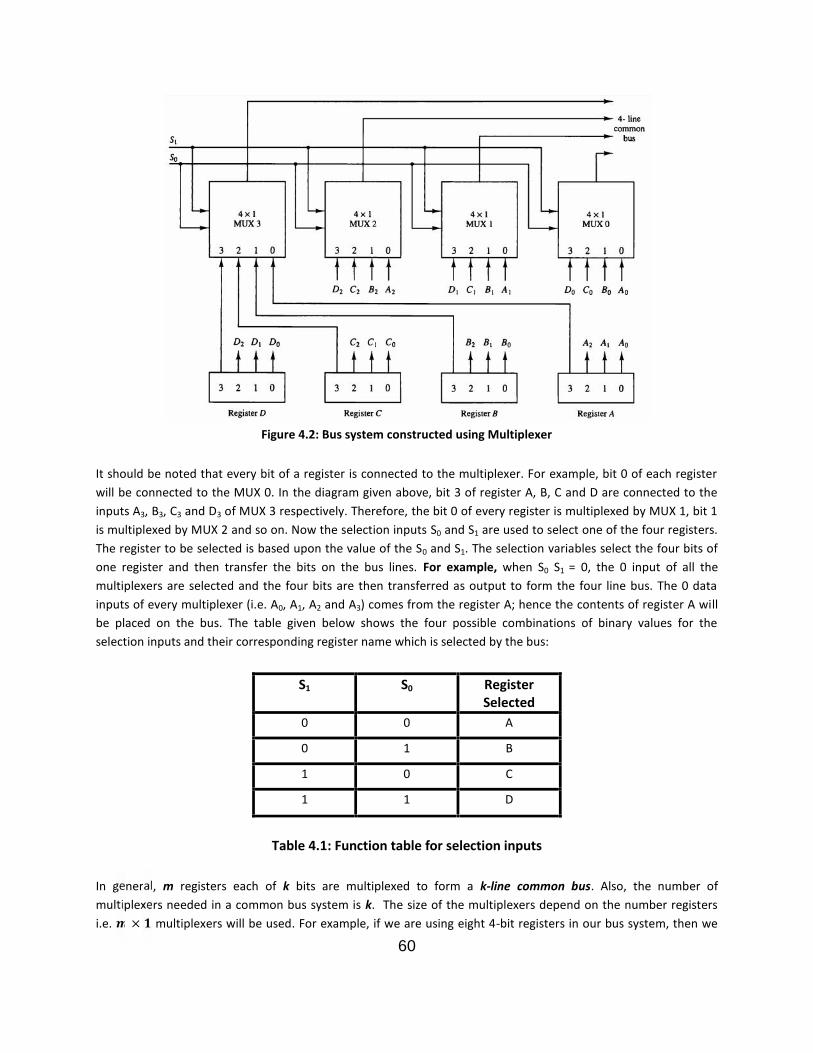
60
Figure 4.2: Bus system constructed using Multiplexer
It should be noted that every bit of a register is connected to the multiplexer. For example, bit 0 of each registerwill be connected to the MUX 0. In the diagram given above, bit 3 of register A, B, C and D are connected to theinputs A3, B3, C3 and D3 of MUX 3 respectively. Therefore, the bit 0 of every register is multiplexed by MUX 1, bit 1is multiplexed by MUX 2 and so on. Now the selection inputs S0 and S1 are used to select one of the four registers.The register to be selected is based upon the value of the S0 and S1. The selection variables select the four bits ofone register and then transfer the bits on the bus lines. For example, when S0 S1 = 0, the 0 input of all themultiplexers are selected and the four bits are then transferred as output to form the four line bus. The 0 datainputs of every multiplexer (i.e. A0, A1, A2 and A3) comes from the register A; hence the contents of register A willbe placed on the bus. The table given below shows the four possible combinations of binary values for theselection inputs and their corresponding register name which is selected by the bus:
Table 4.1: Function table for selection inputs
In general, m registers each of k bits are multiplexed to form a k-line common bus. Also, the number ofmultiplexers needed in a common bus system is k. The size of the multiplexers depend on the number registersi.e. × multiplexers will be used. For example, if we are using eight 4-bit registers in our bus system, then we
S1 S0 RegisterSelected
0 0 A
0 1 B
1 0 C
1 1 D
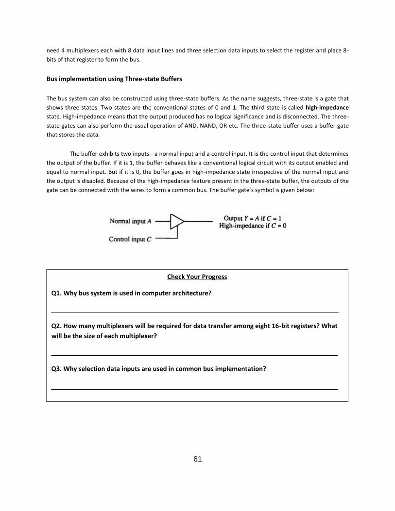
61
need 4 multiplexers each with 8 data input lines and three selection data inputs to select the register and place 8-bits of that register to form the bus.
Bus implementation using Three-state Buffers
The bus system can also be constructed using three-state buffers. As the name suggests, three-state is a gate thatshows three states. Two states are the conventional states of 0 and 1. The third state is called high-impedancestate. High-impedance means that the output produced has no logical significance and is disconnected. The three-state gates can also perform the usual operation of AND, NAND, OR etc. The three-state buffer uses a buffer gatethat stores the data.
The buffer exhibits two inputs - a normal input and a control input. It is the control input that determinesthe output of the buffer. If it is 1, the buffer behaves like a conventional logical circuit with its output enabled andequal to normal input. But if it is 0, the buffer goes in high-impedance state irrespective of the normal input andthe output is disabled. Because of the high-impedance feature present in the three-state buffer, the outputs of thegate can be connected with the wires to form a common bus. The buffer gate’s symbol is given below:
Check Your Progress
Q1. Why bus system is used in computer architecture?
Q2. How many multiplexers will be required for data transfer among eight 16-bit registers? Whatwill be the size of each multiplexer?
Q3. Why selection data inputs are used in common bus implementation?
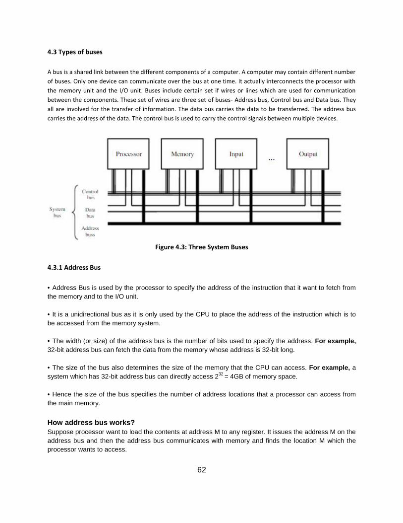
62
4.3 Types of buses
A bus is a shared link between the different components of a computer. A computer may contain different numberof buses. Only one device can communicate over the bus at one time. It actually interconnects the processor withthe memory unit and the I/O unit. Buses include certain set if wires or lines which are used for communicationbetween the components. These set of wires are three set of buses- Address bus, Control bus and Data bus. Theyall are involved for the transfer of information. The data bus carries the data to be transferred. The address buscarries the address of the data. The control bus is used to carry the control signals between multiple devices.
Figure 4.3: Three System Buses
4.3.1 Address Bus
Address Bus is used by the processor to specify the address of the instruction that it want to fetch fromthe memory and to the I/O unit.
It is a unidirectional bus as it is only used by the CPU to place the address of the instruction which is tobe accessed from the memory system.
The width (or size) of the address bus is the number of bits used to specify the address. For example,32-bit address bus can fetch the data from the memory whose address is 32-bit long.
The size of the bus also determines the size of the memory that the CPU can access. For example, asystem which has 32-bit address bus can directly access 232 = 4GB of memory space.
Hence the size of the bus specifies the number of address locations that a processor can access fromthe main memory.
How address bus works?Suppose processor want to load the contents at address M to any register. It issues the address M on theaddress bus and then the address bus communicates with memory and finds the location M which theprocessor wants to access.
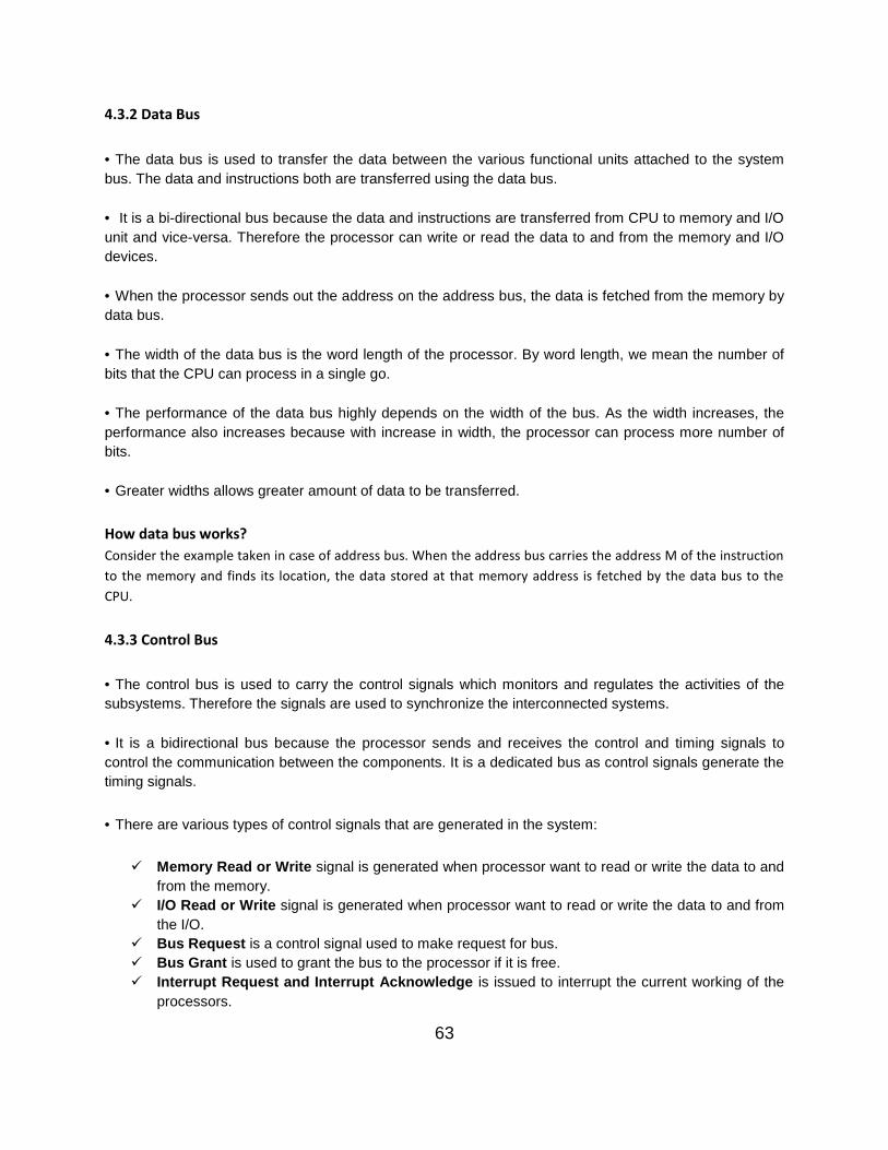
63
4.3.2 Data Bus
The data bus is used to transfer the data between the various functional units attached to the systembus. The data and instructions both are transferred using the data bus.
It is a bi-directional bus because the data and instructions are transferred from CPU to memory and I/Ounit and vice-versa. Therefore the processor can write or read the data to and from the memory and I/Odevices.
When the processor sends out the address on the address bus, the data is fetched from the memory bydata bus.
The width of the data bus is the word length of the processor. By word length, we mean the number ofbits that the CPU can process in a single go.
The performance of the data bus highly depends on the width of the bus. As the width increases, theperformance also increases because with increase in width, the processor can process more number ofbits.
Greater widths allows greater amount of data to be transferred.
How data bus works?Consider the example taken in case of address bus. When the address bus carries the address M of the instructionto the memory and finds its location, the data stored at that memory address is fetched by the data bus to theCPU.
4.3.3 Control Bus
The control bus is used to carry the control signals which monitors and regulates the activities of thesubsystems. Therefore the signals are used to synchronize the interconnected systems.
It is a bidirectional bus because the processor sends and receives the control and timing signals tocontrol the communication between the components. It is a dedicated bus as control signals generate thetiming signals.
There are various types of control signals that are generated in the system:
Memory Read or Write signal is generated when processor want to read or write the data to andfrom the memory.
I/O Read or Write signal is generated when processor want to read or write the data to and fromthe I/O.
Bus Request is a control signal used to make request for bus. Bus Grant is used to grant the bus to the processor if it is free. Interrupt Request and Interrupt Acknowledge is issued to interrupt the current working of the
processors.
64
Reset is used to reset the processor state. Clock signal is used to set the clock pulse.
How control bus works?When the address bus carries the address, the processor also issues a memory read control signal. The data busmust fetch the data from the destined address till this signal is enabled or active.
4.3.4 Complications in single bus system
1. Using single bus in the system can lead to time delays if the number of devices attached to it is more innumber.2. Efficiency of the bus is reduced because of long data paths that are needed to connect all the devices.3. Processor needs to depend on the single bus to communicate with the devices and the memory unit.Using multiple buses, processor can directly connect to the chip on the motherboard where the bus actsas an interface.
4.4 Data movement among Registers using Common Bus
Common bus system is implemented for transferring information in multi-register computing environment. It isused to avoid the heavy circuitry of separate wire connections between the registers and also to speed up thetransfers. It also maintains the synchronization between the various components of the computer. The commonbus system structure consists of common lines or wires which are connected to each bit of every register andtransfers the binary data one at a time. There are control signals that select the register involved in data transfer.The 8 registers in the basic computer architecture are described below-
Register Name Number of Bits Function
Data register (DR) 16 Holds memory data
Check Your Progress
Q4. Name some control singles that are generated by control bus?
Q5. What does the size of the address bus determines?
Q6. The size of the data bus determines the
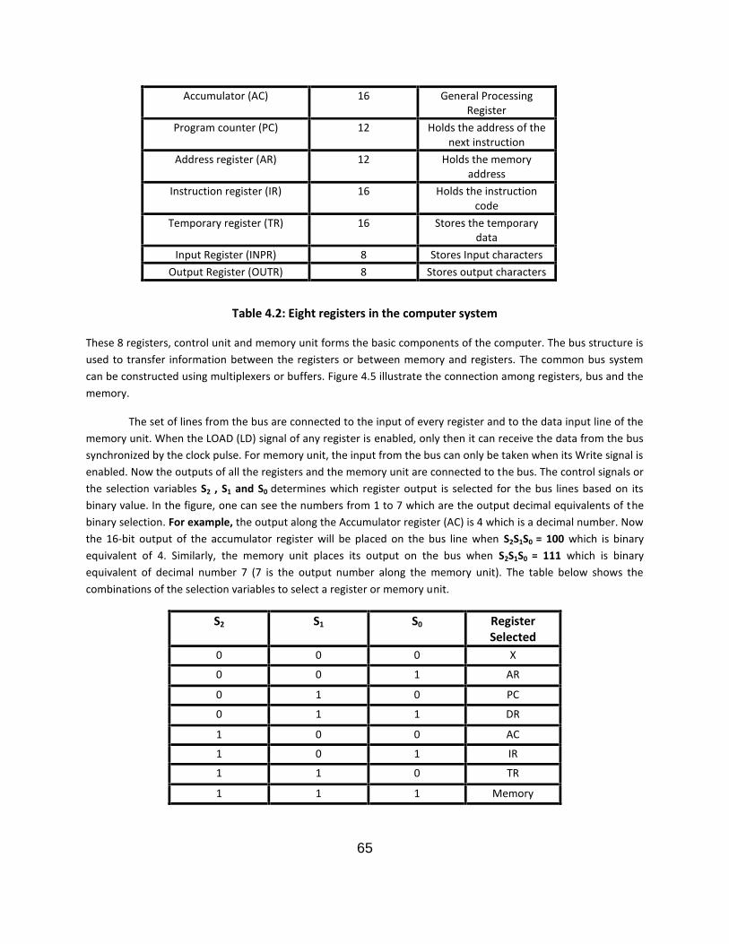
65
Accumulator (AC) 16 General ProcessingRegister
Program counter (PC) 12 Holds the address of thenext instruction
Address register (AR) 12 Holds the memoryaddress
Instruction register (IR) 16 Holds the instructioncode
Temporary register (TR) 16 Stores the temporarydata
Input Register (INPR) 8 Stores Input charactersOutput Register (OUTR) 8 Stores output characters
Table 4.2: Eight registers in the computer system
These 8 registers, control unit and memory unit forms the basic components of the computer. The bus structure isused to transfer information between the registers or between memory and registers. The common bus systemcan be constructed using multiplexers or buffers. Figure 4.5 illustrate the connection among registers, bus and thememory.
The set of lines from the bus are connected to the input of every register and to the data input line of thememory unit. When the LOAD (LD) signal of any register is enabled, only then it can receive the data from the bussynchronized by the clock pulse. For memory unit, the input from the bus can only be taken when its Write signal isenabled. Now the outputs of all the registers and the memory unit are connected to the bus. The control signals orthe selection variables S2 , S1 and S0 determines which register output is selected for the bus lines based on itsbinary value. In the figure, one can see the numbers from 1 to 7 which are the output decimal equivalents of thebinary selection. For example, the output along the Accumulator register (AC) is 4 which is a decimal number. Nowthe 16-bit output of the accumulator register will be placed on the bus line when S2S1S0 = 100 which is binaryequivalent of 4. Similarly, the memory unit places its output on the bus when S2S1S0 = 111 which is binaryequivalent of decimal number 7 (7 is the output number along the memory unit). The table below shows thecombinations of the selection variables to select a register or memory unit.
S2 S1 S0 RegisterSelected
0 0 0 X0 0 1 AR
0 1 0 PC0 1 1 DR
1 0 0 AC1 0 1 IR1 1 0 TR
1 1 1 Memory
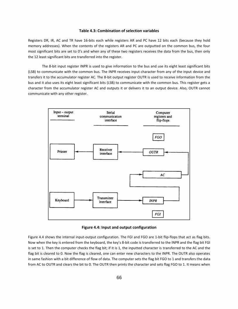
66
Table 4.3: Combination of selection variables
Registers DR, IR, AC and TR have 16-bits each while registers AR and PC have 12 bits each (because they holdmemory addresses). When the contents of the registers AR and PC are outputted on the common bus, the fourmost significant bits are set to 0’s and when any of these two registers receives the data from the bus, then onlythe 12 least significant bits are transferred into the register.
The 8-bit input register INPR is used to give information to the bus and use its eight least significant bits(LSB) to communicate with the common bus. The INPR receives input character from any of the input device andtransfers it to the accumulator register AC. The 8-bit output register OUTR is used to receive information from thebus and it also uses its eight least significant bits (LSB) to communicate with the common bus. This register gets acharacter from the accumulator register AC and outputs it or delivers it to an output device. Also, OUTR cannotcommunicate with any other register.
Figure 4.4: Input and output configuration
Figure 4.4 shows the internal input-output configuration. The FGI and FGO are 1-bit flip-flops that act as flag bits.Now when the key is entered from the keyboard, the key’s 8-bit code is transferred to the INPR and the flag bit FGIis set to 1. Then the computer checks the flag bit; if it is 1, the inputted character is transferred to the AC and theflag bit is cleared to 0. Now the flag is cleared, one can enter new characters to the INPR. The OUTR also operatesin same fashion with a bit difference of flow of data. The computer sets the flag bit FGO to 1 and transfers the datafrom AC to OUTR and clears the bit to 0. The OUTR then prints the character and sets flag FGO to 1. It means when
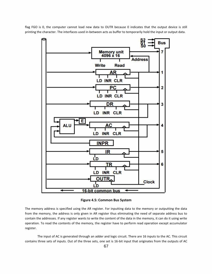
67
flag FGO is 0, the computer cannot load new data to OUTR because 0 indicates that the output device is stillprinting the character. The interfaces used in-between acts as buffer to temporarily hold the input or output data.
Figure 4.5: Common Bus System
The memory address is specified using the AR register. For inputting data to the memory or outputting the datafrom the memory, the address is only given in AR register thus eliminating the need of separate address bus tocontain the addresses. If any register wants to write the content of the data in the memory, it can do it using writeoperation. To read the contents of the memory, the register have to perform read operation except accumulatorregister.
The input of AC is generated through an adder and logic circuit. There are 16 inputs to the AC. This circuitcontains three sets of inputs. Out of the three sets, one set is 16-bit input that originates from the outputs of AC
68
itself. These are used to perform operations like complement, shift etc. Second set of 16-bit inputs come from DR.These are used to perform the arithmetic and logical operations like SUB DR from AC, MUL DR to AC. The results ofsuch operations are transferred to AC and if any carry-out or borrow-in is required, it is stored in flip-flop E. Thelast set of 8-bit inputs comes from the INPR register like inputting an alphabet from the keyboard to AC.
The 16-bit common bus has 16 lines connected to the six registers (as input register gives information tothe bus) and the memory unit to receive information from them. From the above figure, it can be seen that thereare three control inputs connected to five registers: Load (LD), Increment (INR) and Clear (CLR). The INR isequivalent to binary counters which are used to count the number of events that occur due to input signals appliedto the register. It also generates timing signals that is used to control the sequence of operations in computers.The LD input is used to load the new information into the register. The CLR is used to clear the contents of theregister i.e. to make all the bits of the register to 0. There are two registers that have only one input- LD.
It can be seen that the contents of the register can be applied onto the common bus and at the same time,operations can be performed in the arithmetic and logic unit. It means that the transfer and the operations can beperformed during the same clock cycle. The data can be transferred from one register to another using the 16- bitcommon bus. This can be done by loading the contents of one register onto the bus and then transferring thecontents from the bus to the destined register. For example, consider the two operations-
It means that first the contents from AC are placed onto the bus by enabling the select variables as S2S1S0 = (100)2 =(4)10 (i.e. decimal equivalent is 4). Then the bus transfers the contents of the AC to DR by enabling DR’s LD input.Now the content of the DR is transferred to AC through adder and logic circuit and by enabling AC’s LD input.Usually we do not write the word BUS during the transfers, it can simply be written as:
These two operations can be executed at the same time. These all steps are performed during the same clockcycle. It should be noted that the clock transition at the end of the clock cycle make the transfers from bus to thedestined register and from the adder-logic circuit to the AC.
Data movement among Registers and Memory
Using common bus, data can be transferred among registers and the memory system. To read the memory wordor transfer the word from the memory to other devices is called a read operation. Whereas to write bytes ofinformation into the memory is called write operation. The memory word which is to be read or write is denotedby M. The address of this memory word is specified in square brackets. Now consider an example where the ACregister writes the word to memory.
BUS ←ACDR←BUSAC←DR
DR ← AC and AC ← DR
69
Here the contents of AC register to be transferred to the memory word M whose address is selected by addressregister AR. The write operation is done only when the write signal is enabled of the memory unit.
4.5 Summary
The computer basically consists of memory system, processor and some input-output devices. To providecommunication between the various components of the computer, bus system is used. A bus is a finite set of wiresor lines that connects the subsystems together and provide data transfer among them. The bus can be constructedusing the multiplexers that select the registers whose output has to be placed on the bus and then is transferred tothe other register or some other device. The bus can also be constructed using three-state buffers. There are threetypes of system buses available. Address bus is used to provide address of the memory word to be accessed by theprocessor. Data bus is used to carry the data which is fetch from the memory location specified by the address bus.Control bus provides the control signals to monitor the activities running in the system. But in order to lower thecomplexity and the additional cost of having three buses, we can use a common bus that contains various registersto perform the transfer among them and also between the register and memory or input-output. Data movementcan be performed among the registers by using common bus.
M[AR] ←AC
Check Your Progress
Q7. Given below are the register transfers which are to be executed in the bus system. For each transfer,specify
(a). The binary data values for selection variables.
(b). Which register’s load input has to be enabled?
i. AR←PCii. PC←TR
Q8. Write a bus transfer operation if temporary register wants to write its content in memory?

70
4.6Glossary
Address Bus- Address Bus is used by the processor to specify the address of the instruction that itwant to fetch from the memory and to the I/O unit. Bus- A bus is set of wires or lines used to provide communication among the components of computer. Clear input-The CLR is used to clear the contents of the register i.e. to make all the bits of the registerto 0. Control Bus- The control bus is used to carry the control signals which monitors and regulates theactivities of the subsystems. Data Bus- The data bus is used to transfer the data between the various functional units attached to thesystem bus. Increment input-The INR is equivalent to binary counters which are used to count the number ofevents that occur due to input signals applied to the register. It also generates timing signals that is usedto control the sequence of operations in computers. Load input-The LD input is used to load the new information into the register. Memory Read Operation- Read operation means to read the memory word or to transfer the word fromthe memory to other devices Memory Write Operation- Write operation means to write a word into the memory.
4.7Answers to Check Your Progress/ Suggested Answers to SAQ
1. Bus system is used in computer architecture in order to provide communication between the variouscomponents of computer like processor, memory unit and I/O system. It acts as an interface between the variousdevices. Bus system is just like a communication link to provide data transfers.
2. The number of multiplexers needed will be 16. The size of multiplexer will be 8 × 1, i.e. 8 input data lines in eachmultiplexer is needed.
3. The selection data inputs are used to select one of the four registers. The selection variables select the four bitsof one register and then transfer the bits on the bus lines.
4. Some of the control signals used are - memory read or write, bus request, bus grant, interrupt request, interruptacknowledgement etc.
5. The size of the address bus determines the size of the memory that the CPU can access.
6. The size of the data bus determines the word length of the processor.
7. For AR←PC
(a) The binary values for selection variables for this transfer is- S2S1S0 = 010. As here the data contents ofPC will be placed on the bus by enabling its selection inputs.
(b) The load input of AR register will be enabled to load the contents of PC.
For PC←TR

71
(a) The binary values for selection variables for this transfer is- S2S1S0 =110. As here the data contents ofTR will be placed on the bus by enabling its selection inputs.
(b) The load input of PC register will be enabled to load the contents of TR.
8. M[AR]←TR
4.8 Terminal and Model Questions
1. Explain the construction of bus system using multiplexers?
2. List the names, number of bits and functions of 8 registers used in computer organization?
3. Explain in detail the three types of system buses?
4. Draw the diagram showing the connection between the common bus and the registers. Explain in detail?
5. How the data is transferred among registers using the common bus?

72
Lesson 5
Basic Computer Instructions
Structure
5.0 Objectives
5.1 Introduction
5.2 Computer Instructions
5.3 Direct and Indirect Address
5.4 Types of Instructions
5.4.1 Memory Reference Instructions5.4.2 Register Reference Instructions5.4.3 Input-Output Reference Instructions
5.5 Instruction Formats
5.5.1 Three Address Instructions5.5.2 Two Address Instructions5.5.3 One Address Instructions5.5.4 Zero Address Instructions
5.6 Instruction Cycles
5.7 Summary
5.8 Glossary
5.9 Answer to Check Your Progress/Suggested Answers to SAQ
5.10 Bibliography/ References/ Suggested Readings
5.11 Terminal and Model Questions
5.0 Objectives
After studying this chapter you will understand
The basic structure of computer instructions.
What is direct and indirect addressing?
Types of instructions.
Various instruction formats.
73
How the computers distinguish between various computer instructions?
Instruction cycle
5.1 Introduction
This chapter provides the information about the types of instructions in the computer systems. Instructionsare the commands given to the computers to do specific task. The instructions are basically the group of bits.These groups of bits may be arranged in different patterns for different instructions. There are three types ofinstructions memory reference instructions, register reference instructions and input output referenceinstructions. The chapter also discuss the various instruction formats. The instruction may be of three addressinstructions, two address instructions, one address instruction and zero address instructions. The instructiondecoder decodes the instructions; accordingly the control unit issues the set of micro operations to do the desiretask. The necessary operations to fetch and execute the instruction constitute the instruction cycle.
5.2 Computer Instructions
Instructions are the commands given to the computer to perform a specific operation. It resides in the memoryunit of the computer. Computer instructions are basically the set of binary codes. These binary codes are a groupof bits that instructs the computer to perform certain task. The instruction code is divided into two parts.
Operation code Operands
Operation code: The operation code of the instruction specifies the operation to be performed. It is also calledopcode. The operations that instructions can perform are addition, subtraction, multiplication, division;complements etc .The total number of bits required for operation code depends upon the number of operation tobe performed. If opcode is of n bits then it can specify 2n different operations. For example 64 operations can bespecified by 6 bit of opcode.
Operands: The operation code must perform operation on the data present in the instruction. The data part of theinstruction is called operand. The operand may be the actual data on which operation is performed or it mayregister/ memory word address where the data is stored.
Figure 1 Instruction Code
The computer reads an instruction from the memory and places it on the control register. The control register theninterprets its meaning and issues the necessary sequence of operation to do the task.
There are many ways for arranging the binary codes in the instructions. Depending upon the design, eachcomputer has their particular instruction code. Instruction may be 8 bit, 16 bit or 32 bit long. The instruction lengthtotally depends upon the register used by the system. So every computer has unique instruction set.
5.3 Direct and Indirect Address
OPCODE OPERAND
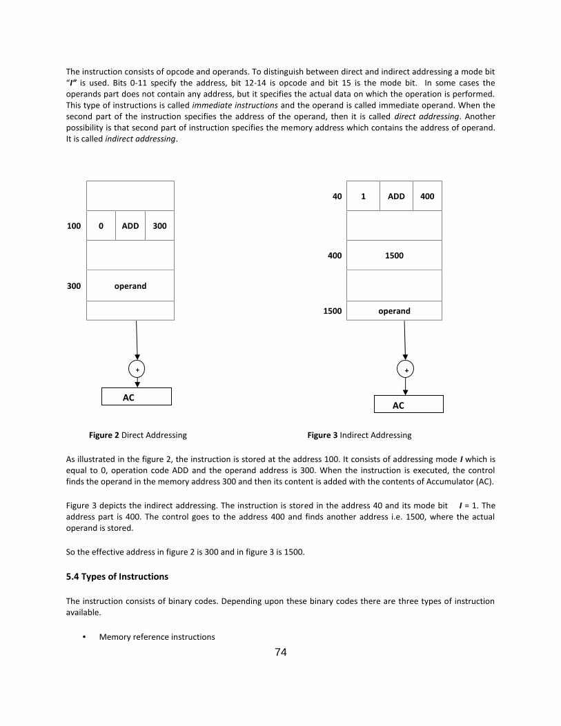
74
The instruction consists of opcode and operands. To distinguish between direct and indirect addressing a mode bit“I” is used. Bits 0-11 specify the address, bit 12-14 is opcode and bit 15 is the mode bit. In some cases theoperands part does not contain any address, but it specifies the actual data on which the operation is performed.This type of instructions is called immediate instructions and the operand is called immediate operand. When thesecond part of the instruction specifies the address of the operand, then it is called direct addressing. Anotherpossibility is that second part of instruction specifies the memory address which contains the address of operand.It is called indirect addressing.
40 1 ADD 400
100 0 ADD 300
400 1500
300 operand
1500 operand
Figure 2 Direct Addressing Figure 3 Indirect Addressing
As illustrated in the figure 2, the instruction is stored at the address 100. It consists of addressing mode I which isequal to 0, operation code ADD and the operand address is 300. When the instruction is executed, the controlfinds the operand in the memory address 300 and then its content is added with the contents of Accumulator (AC).
Figure 3 depicts the indirect addressing. The instruction is stored in the address 40 and its mode bit I = 1. Theaddress part is 400. The control goes to the address 400 and finds another address i.e. 1500, where the actualoperand is stored.
So the effective address in figure 2 is 300 and in figure 3 is 1500.
5.4 Types of Instructions
The instruction consists of binary codes. Depending upon these binary codes there are three types of instructionavailable.
Memory reference instructions
+ +
ACAC
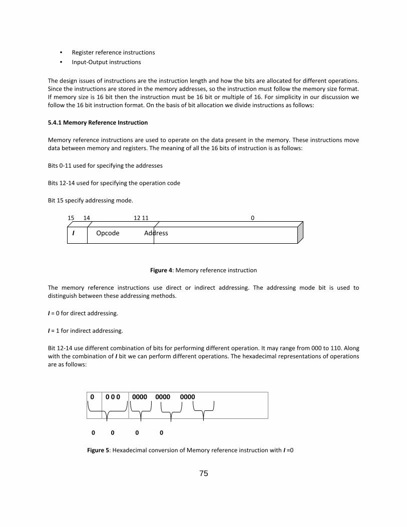
75
Register reference instructions Input-Output instructions
The design issues of instructions are the instruction length and how the bits are allocated for different operations.Since the instructions are stored in the memory addresses, so the instruction must follow the memory size format.If memory size is 16 bit then the instruction must be 16 bit or multiple of 16. For simplicity in our discussion wefollow the 16 bit instruction format. On the basis of bit allocation we divide instructions as follows:
5.4.1 Memory Reference Instruction
Memory reference instructions are used to operate on the data present in the memory. These instructions movedata between memory and registers. The meaning of all the 16 bits of instruction is as follows:
Bits 0-11 used for specifying the addresses
Bits 12-14 used for specifying the operation code
Bit 15 specify addressing mode.
15 14 12 11 0
Figure 4: Memory reference instruction
The memory reference instructions use direct or indirect addressing. The addressing mode bit is used todistinguish between these addressing methods.
I = 0 for direct addressing.
I = 1 for indirect addressing.
Bit 12-14 use different combination of bits for performing different operation. It may range from 000 to 110. Alongwith the combination of I bit we can perform different operations. The hexadecimal representations of operationsare as follows:
0 0 0 0
Figure 5: Hexadecimal conversion of Memory reference instruction with I =0
0 0 0 0 0000 0000 0000
I Opcode Address
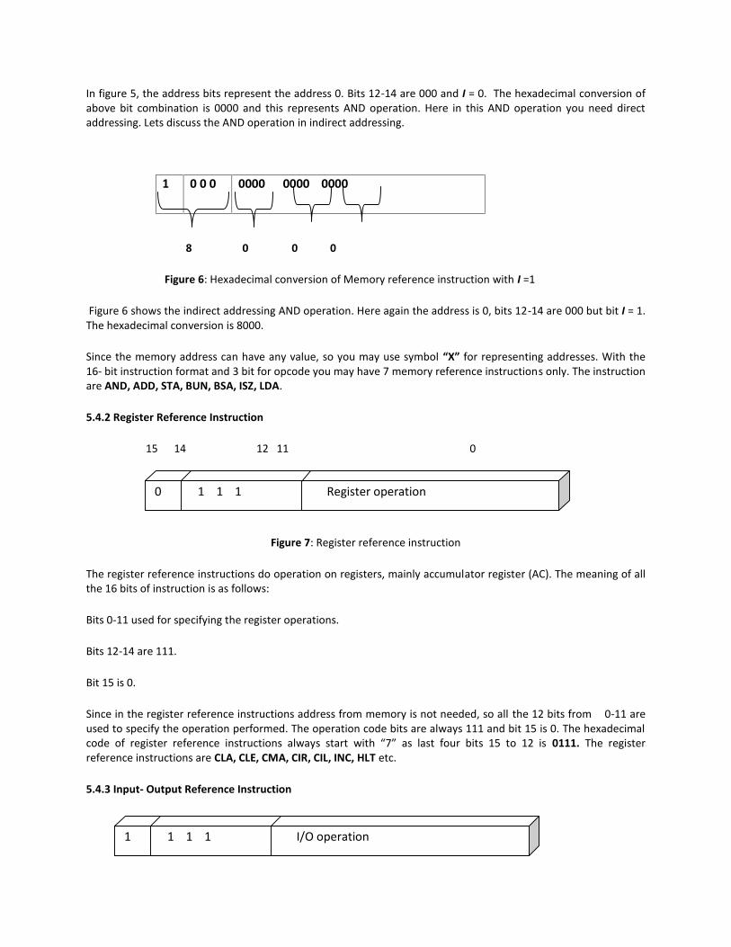
76
In figure 5, the address bits represent the address 0. Bits 12-14 are 000 and I = 0. The hexadecimal conversion ofabove bit combination is 0000 and this represents AND operation. Here in this AND operation you need directaddressing. Lets discuss the AND operation in indirect addressing.
8 0 0 0
Figure 6: Hexadecimal conversion of Memory reference instruction with I =1
Figure 6 shows the indirect addressing AND operation. Here again the address is 0, bits 12-14 are 000 but bit I = 1.The hexadecimal conversion is 8000.
Since the memory address can have any value, so you may use symbol “X” for representing addresses. With the16- bit instruction format and 3 bit for opcode you may have 7 memory reference instructions only. The instructionare AND, ADD, STA, BUN, BSA, ISZ, LDA.
5.4.2 Register Reference Instruction
15 14 12 11 0
Figure 7: Register reference instruction
The register reference instructions do operation on registers, mainly accumulator register (AC). The meaning of allthe 16 bits of instruction is as follows:
Bits 0-11 used for specifying the register operations.
Bits 12-14 are 111.
Bit 15 is 0.
Since in the register reference instructions address from memory is not needed, so all the 12 bits from 0-11 areused to specify the operation performed. The operation code bits are always 111 and bit 15 is 0. The hexadecimalcode of register reference instructions always start with “7” as last four bits 15 to 12 is 0111. The registerreference instructions are CLA, CLE, CMA, CIR, CIL, INC, HLT etc.
5.4.3 Input- Output Reference Instruction
1 0 0 0 0000 0000 0000
0 1 1 1 Register operation
1 1 1 1 I/O operation
77
Figure 8: Input- Output reference instruction
Input-Output instructions perform operations related to input and output like input character in AC, setting flags,handling interrupts etc. Similar to register reference instructions, these instructions need not to specify thememory addresses, so the bits 0-11 are used to specify the input output operations or related test operations only.
Bits 0-11 used for specifying the I/O operations.
Bits 12-14 are 111.
Bit 15 is 1.
The last four bits of these instructions are 1111. So hexadecimal code of input output instructions always start with“F”. The I/O instructions and their respected hexadecimal codes are:
Symbol Hexadecimal code Operations
INP F800 input the value to AC
OUT F400 output the value to AC
SKI F200 skip on input flag
SKO F100 skip on the out flag
ION F080 interrupts on
IOF F040 interrupts off
The total number of instructions chosen for the basic computer is 25.
Self Assessment 1
Q1. What are instructions? Name the various fields of instructions.
Sol. __________________________________________________________________________
__________________________________________________________________________
__________________________________________________________________________
__________________________________________________________________________
Q2. Name the different types of instructions.
Sol. __________________________________________________________________________
78
__________________________________________________________________________
__________________________________________________________________________
Q3. If the opcode is 4 bit long, then how many operations can be specified by that instruction?
Sol. __________________________________________________________________________
__________________________________________________________________________
__________________________________________________________________________
Q4. Mode Bit “I” = 0 in memory reference instruction stands for __________ addressing.
Q5. Hexadecimal code of register reference instruction start with _____ and I/O referenceinstruction starts with ______________.
5.5 Instruction Format
The format of instruction depends upon the construction of the CPU, type of processor register available and thelogical capabilities of these registers. Depending upon these parameters the computers usually have variety ofinstruction code formats. So, the function of control unit in the CPU becomes very critical. The control unitinterprets the meaning of each instruction code and provides the needed control functions to process theinstruction.
The computer instructions consist up of binary bits. These bits are divided into various groups called the fields. Themost common fields found in the instruction are:
Address field: specify the memory address or processor registers
Operation code: this field specifies the operation to be performed.
Mode field: it specifies the way in which operand is accessed or effective address is determined.
We distinguish various instruction formats on the basis of address field. The address field may be single address ormultiple addresses.
The computer instructions may be of varied length, depending upon the number of address fields. The number ofthe address fields further depends upon the internal organization of registers. The computers has following typesof CPU organization
Single Accumulator Organization
General Register Organization
Stack Organization

79
Single Accumulator Organization: In these computer systems, all the operation considers the implied accumulatorregister. The instruction format has only one register as the other register is accumulator. For example, the ADDoperation in assembly language is as follows
ADD X
Here X is the address of the operand. The ADD instruction needs two operands, so it is understood that otheroperand is stored in the AC register. The above ADD instruction results in the operation:
AC AC + M[X]
M[X] represents the memory word store in the address X. Here we can say that the content of AC is added withthe memory word store at address X and result is again store back to Accumulator.
General Register Organization: The instruction format of this type of computer needs three register addresses inthe address field. The ADD instruction in this computer is written as:
ADD REG1, REG2, REG3
The operation of above instruction is
REG1 REG2 + REG3
The contents of register REG2, REG3 is added and stored in REG1.
We can reduce the number of address register from three to two, if out of two source registers one will act asdestination register also. The ADD operation in this case becomes
ADD REG1, REG2
The operation of above instruction is
REG1 REG1 + REG2
In this type of computer we can also add the contents of registers with the contents of memory addresses. So theaddress field contains one register address and another, memory address. It can be symbolized as follows:
ADD REG1, X
Operation as:
REG1 REG1 + M[X]
Stack Organization: computers with stack organization have PUSH and POP instructions to manipulate the stack.These instructions require an address field.
PUSH X
It will push the word at the memory location X to the stack top. The address of the stack top is stored in the stackpointer.
80
The operational instructions in the stack organization do not need any address field. This is because the operationis performed on the two top locations of the stack. The ADD instruction is written as:
ADD
This instruction pops two top locations of stack and then performs ADD operation and result is stored back to newstack top. There is no need to specify the operand and address field in this instruction.
Most of the computers fall in these three categories, but you can also have systems with combined features ofabove types of organizational structures.
Depending upon the numbers of address fields in the instruction format we can also categorizes the instructionsinto
Three Address Instructions
Two Address Instructions
One Address Instructions
Zero Address Instructions
Let’s understand all these types of instruction formats by performing following operation
X = A + B
5.5.1 Three Address Instructions
The computer with three address format can use three address fields to implement above operation. The addressfield may have register addresses and memory addresses both. The instruction in assembly language is written as
ADD X, A, B
The operation of instruction is
M [X] M [A] + M [B]
In the instruction we have three address fields. The advantage of three address instruction is that we get resultswith short programs. The disadvantage is that we need too many bits to specify the addresses.
5.5.2 Two Address Instructions
Two address instructions use two addresses in the address field. It is more common in the commercial computers.Here we use MOV instruction to transfer the operands to and from memory and registers. The said instruction isevaluated as follows:
MOV REG1, A
ADD REG1, B
81
MOV X, REG1
Operation as follows:
REG1 M [A]
REG1 REG1 + M [B]
M [X] REG1
5.5.3 One Address Instructions
One address instructions has one address in the address field and use an implied accumulator register (AC) forperforming the data manipulations. We do not need any second register and assume that accumulator registercontains the result of all operations. LOAD and STORE instructions are used to evaluate the said instructions.
LOAD A
ADD B
STORE X
Operations as follows:
AC M [A]
AC AC + M [B]
M [X] AC
As the number of operations increases in the one address instruction, we may have to use some temporarymemory locations to store the accumulator values or some intermediate results. The temporary location isdenoted by symbol T.
5.5.4 Zero Address Instructions
Zero address instructions used in the stack organization computers. The instructions need not specify any addressvalue. Since all the operations are performed on the stack, we need PUSH and POP operations. These instructionswork on the top of stack (TOS). To evaluate the above said instruction we must convert it into reverse polishnotation i.e. AB+.
PUSH A
PUSH B
ADD
POP X
Operations as follows:

82
TOS A
TOS B
M [X] TOS
In zero address instruction formats we need very large numbers of instructions to evaluate the same expression, ascompared to other instructions formats.
5.6 Instruction Cycle
The set of instructions to do a specific task is called program. These programs reside in the memory unit ofcomputer system. CPU fetch an instruction from the memory and then perform steps for executing the instruction.This fetch cycle and execution cycle constitute the instruction cycle. The instruction cycle is further subdivided intosub cycles. In the basic computer the instruction cycle has following phases:
1. Fetch Cycle: in this phase instruction is fetched from the memory.2. Decode the instruction3. Read the address of the operand from memory4. Execute the instruction
After the completion of step 4, the control goes back to step 1 to fetch new instruction. This process continuesuntil we encountered the HALT instruction.
Instruction in CPU
Execution complete
Reset halt instruction encountered
Figure 9: Instruction Cycle
Fetch and Decode
During the fetch operation, instruction is read from the memory. The fetch cycle has following steps:
Program Counter (PC) is loaded with the memory address of first instruction of program.
Instruction code is read from memory and placed on the Instruction Register (IR).
Program Counter is incremented to new address.
After the instruction is read from the memory, it is sent to instruction decoder. The instruction decoder decodesthe instruction and then the type of instruction is specified on the basis of size or task to be completed. The threetype of instruction is available in basic computer. Here IR represents instruction register.
Fetch Execute
HALT

83
IR (15) = 0 IR (12-14) =1 1 1 IR (0 – 11) = Register operation
If bit 15 is 0 and opcode bit is 111, the instruction type is register reference instruction.
IR (15) = 1 IR (12-14) =1 1 1 IR (0 – 11) = I/O operation
If bit 15 is 1 and opcode bit is 111, the instruction type is input / output reference instruction.
IR (15) = I IR (12-14) =000 through 110 IR (0 – 11) = address
If bit 15 is mode bit I and opcode bits range from 000 to 011, the instruction type is memory reference instruction.Mode bit 0 indicates direct addressing and 1 indicates indirect addressing.
Fetch operands from memory if necessary
In the instruction cycle if the instruction contains the data part then the instruction is executed immediately and ifthe instruction needs operand from other memory location then first, the operand is read from memory and thenexecution operation takes place.
Execute the instruction
The fetched instruction is loaded into the register known as Instruction Register (IR). The instruction contains thebits that specify the action that processor has to perform. Processor action generally comes under followingcategories:
Processor / Memory transfer : data may be transferred from memory to processor or from processor to memory.
Processor /Input-output: data may transfer from I/O to processor or from processor to I/O.
Data Processing: in this category the processor may perform some arithmetic or logic operations.
Control: These instructions are used to control the sequence of execution.
The instruction execution may involve the combination of all above operations.
The total time required to completely execute the instruction is
IC = FC + EC
IC: Time required to execute the instruction.
FC: Fetch cycle time
EC: Execute cycle time
By overlapping fetch and execute cycle, we can execute more than one instruction simultaneously. Pipelineprocessors are build on the same concept.
Self Assessment 2
84
Q1. What are the various steps of executing the instruction?
Sol. ______________________________________________________________________
_______________________________________________________________________
_______________________________________________________________________
Q2. Discuss the purpose of program counter and instruction register.
Sol. _______________________________________________________________________
_______________________________________________________________________
_______________________________________________________________________
Q3. What are the various instruction formats available in the system?
Sol. ________________________________________________________________________
_________________________________________________________________________
_________________________________________________________________________
_________________________________________________________________________
Q4. The phase of instruction cycle in which meaning of instruction is depicted is called
a. Fetch cycle b. Instruction cyclec. Decode cycle d. Execute cycle
Q5. The phases of the Instruction cycle are
a. Fetch b. Decodec. Execute d. None of thesee. All of these
5.7 Summary
Computer is an electronic device and it is used to solve the problems or do the computational tasks. Computersystems use programs to solve the problems. Programs consist of instructions. The Instructions are the commandgiven to the computer. There are three types of instructions. They are, memory reference instructions, registerreference instructions and input-output reference instructions. The set of bits in the instructions are divided intothree fields i.e. address field, operation code field and mode bit field. The number of operation performed by theinstructions depends upon the number of bits of opcode.
The address field may contain memory address or register address. The instructions may have more than oneaddress fields. Depending upon the number of address fields, the instructions are categorized as, three addressinstructions, two address instructions, one address instructions and zero address instructions. Three address
85
instructions are more complicated and need large number of bits but they reduce the number of instructions in aprogram.
The instruction needs a set of phases to completely execute. These phases constitute the instruction cycle. Theinstruction phases are fetching, decoding and executing the instructions. The total time required to completelyexecute the instruction is the sum of instruction cycle time and execute cycle time.
5.8 Glossary
Direct addressing: When the address field of the instruction specifies the address of the operand, then itis called direct addressing.
Execute cycle: the steps perform to execute the instructions constitute the execute cycle. Fetch cycle: during this cycle the instruction is fetched from the memory. Indirect addressing: When the address field of the instruction specifies the address, which contain the
address of the operand, then it is called indirect addressing. Instruction: Instructions are the commands given to the computer to perform a specific operation. Instruction Cycle: The instruction cycle consist of fetch cycle and execute cycle. Instruction Format: The computer instructions may be of varied length, depending upon the number of
address fields instructions has different formats Instruction register: It contains the instruction that is most recently fetched. It is represented by IR. Operation code: The operation code of the instruction specifies the operation to be performed. It is also
called opcode. Operands: The data part of the instruction is called operand. Program: Program is a set of instruction to do a specific task.
5.9 Answer to Check Your Progress/Suggested Answers to SAQ
Self Assessment 1
Solution 1) Instructions are the commands given to the computer to perform a specific operation. It resides in thememory unit of the computer. The various fields of instruction are: Address field, operation code field and Modebit field..Solution 2)
1. Memory Reference Instructions
2. Register Reference Instructions
3. Input-Output Reference Instructions
Solution 3) The total number of operation specified is
24 = 16
Solution 4) Direct

86
Solution 5) 7, F
Self Assessment 2Solution 1)
1. Fetch Cycle the instruction2. Decode the instruction3. Read the address of the operand from memory4. Execute the instruction
.Solution 2) Program Counter Register stores the address of next instruction to be executed. It is
incremented by one after the fetch operation.
Instruction Register is a register that stores the executing instruction.
Solution 3)
1. Three Address instructions
2. Two Address Instructions
3. One Address Instructions
4. Zero Address Instructions
Solution 4) c
Solution 5) e
5.10 Bibliography/ References/ Suggested Readings:
1. Computer System Architecture, M.M. Mano, Third Edition, PHI2. Computer Organization and Architecture Lab.3. Computer Organization and Architecture, Stallings, Eighth Edition, PHI
5.11 Terminal and Model Questions
Q1. What is instruction? Explain different type of instructions
Q2. Explain the meaning of memory reference instruction “STA”.
Q3. Explain any two register reference instructions.
Q4. Explain any two Input-Output reference instructions.
Q5. What do you understand by Opcode and Operands?
Q6. Explain the instruction cycle in detail.
Q7. What are the various instruction format are available? Explain.
Q8. Write an assembly language program to ADD two numbers using two address format
87
Lesson 6
Interrupt
Structure
6.0 Objectives
6.1 Introduction to Interrupt
6.1.1 Interrupt and Use of Stack
6.1.2 Interrupt Vs Polling
6.2 Types of Interrupts
6.3 External Interrupts
6.3.1 I/O Interrupt
6.3.1.1 Data Transfer Interrupt
6.3.1.2 Status Change Interrupt
6.3.1.3 End of I/O Interrupt
6.3.2 Operator Interrupt
6.3.3 Hardware Malfunction Interrupt
6.3.3.1 Error in the External Hardware
6.3.3.2 Power Fail Interrupt
6.3.4 System Management Interrupt
6.4 Internal Interrupts
6.4.1 Internal Hardware Interrupts
6.4.2 Software Interrupts
6.5 Self Assessment Questions (Section 6.1 to 6.4)
6.6 Interrupt Service Sequence
6.7 Interrupt Cycle
6.8 Interrupt Instructions
6.9 Priority Interrupt
6.9.1 Hardware Implementation of Priority Interrupt
6.10 Example of Interrupt Program
6.11 Self Assessment Questions (Section 6.6 to 6.10)
6.12 Summary
6.13 Glossary
6.14 Answers to Check Your Progress/ Self Assessment Questions (SAQ)

88
6.15 Bibliography/References/Suggested Readings
6.16 Terminal and Model Questions
6.0 Objectives To discuss an interrupt process
Difference between different interrupts
To explain interrupt instruction
Steps to initiate and implement interrupts
Interrupt cycle and interrupt execution
Hardware implementation of interrupts
After the completion of this chapter students will be able to understand the basic concept of interrupts, its types
and the process of the interrupt handling by the processor i.e. steps followed by the microprocessor to execute an
interrupt. The understanding of the interrupts and its instructions will enable the students to proceed for writing
various programs to enable interrupts and writing programs for the use of interrupts in different applications.
6.1 Introduction to Interrupt
Interrupt is a process that is initiated by the internal or external devices to have the attention of the CPU to
perform some specific task. When a Process is being executed by the CPU during this if another device request for
execution of another important function immediately, then this new request forces the already Running Process to
stop wherever it is to handle the new request and execute it first. This process of stopping the current execution of
a program to execute the newly requested by some I/O device is called Interrupt. All this process of the interrupt is
automatically controlled by the microprocessor as per the sequence of instructions written for it.
Main Program
1st Instruction
2nd Instruction
3rd Instruction
Interrupt Here
4th Instruction
---------------
---------------
Last Instruction
Interrupt Service
Routine
1st Instruction
2nd Instruction
3rd Instruction
------------
---------------
Return from interrupt
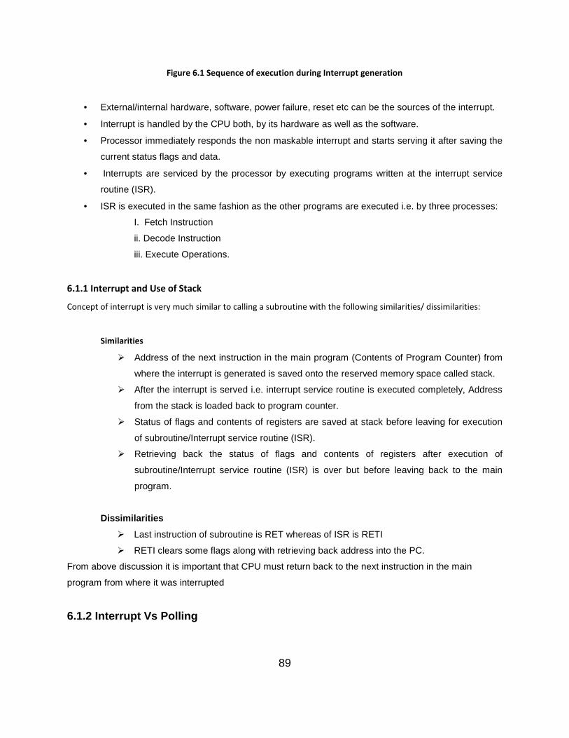
89
Figure 6.1 Sequence of execution during Interrupt generation
External/internal hardware, software, power failure, reset etc can be the sources of the interrupt.
Interrupt is handled by the CPU both, by its hardware as well as the software.
Processor immediately responds the non maskable interrupt and starts serving it after saving the
current status flags and data.
Interrupts are serviced by the processor by executing programs written at the interrupt service
routine (ISR).
ISR is executed in the same fashion as the other programs are executed i.e. by three processes:
I. Fetch Instruction
ii. Decode Instruction
iii. Execute Operations.
6.1.1 Interrupt and Use of Stack
Concept of interrupt is very much similar to calling a subroutine with the following similarities/ dissimilarities:
Similarities
Address of the next instruction in the main program (Contents of Program Counter) from
where the interrupt is generated is saved onto the reserved memory space called stack.
After the interrupt is served i.e. interrupt service routine is executed completely, Address
from the stack is loaded back to program counter.
Status of flags and contents of registers are saved at stack before leaving for execution
of subroutine/Interrupt service routine (ISR).
Retrieving back the status of flags and contents of registers after execution of
subroutine/Interrupt service routine (ISR) is over but before leaving back to the main
program.
Dissimilarities Last instruction of subroutine is RET whereas of ISR is RETI
RETI clears some flags along with retrieving back address into the PC.
From above discussion it is important that CPU must return back to the next instruction in the main
program from where it was interrupted
6.1.2 Interrupt Vs Polling
90
Several devices (Internal/External) are interconnected or interfaced within or with the CPU. Thus CPU has to
provide services to these devices as per the instructions written for these devices. Processor broadly adopts two
methods to serve these devices:
i. Interrupt
ii. Polling
In the interrupt method, when the device that has required services of the CPU to perform some tasks
notifies it to the CPU. The CPU in returns provide services to that device by stopping all other functions
wherever whatever it is running by executing program written on the Interrupt service routine.
On other hand when CPU continuously monitor all the devices connected to it in a particular sequence to
find which device out of these has required its services is called Polling. Here from this discussion it is
clear that CPU wastes its precious time in monitoring the devices irrespective of the services required to
them. Thus using interrupts is the most efficient method for serving the devices interfaced with the
processor. By using this technique a processor can handle a number of tasks at a time, which in results
increases the overall speed of the functioning of the CPU.
6.2 Type of Interrupts
Depending on the source of the interrupt generation, broadly the type of interrupts that alters the sequence of
running of a program are as follows:
1. External interrupts
2. Internal interrupts
6.3 External interrupts
External interrupt is generated by the external devices i.e. outside the CPU (Input/output) by making the pins
where they are connected equal to logic 0 (for active low) and equal to logic 1 (for active high). The causes of
interrupt can be by the interrupted power supply, request from input device to transfer data to CPU or output
device request for data from the CPU. In case of power failure, interrupt generated forces the CPU to run service
routine to save the current status of the devices and registers safely by using internal back up (battery) system.
Other sources of external interrupt may be the error in the external hardware, status change of the I/O, end of I/O
interrupt etc. as per the interrupt flow diagram shown in figure 6.2, External Interrupt is subdivided into the four
categories as:
i. I/O Interrupt
ii. Operator Interrupt
iii. Hardware Malfunction
iv. SMI
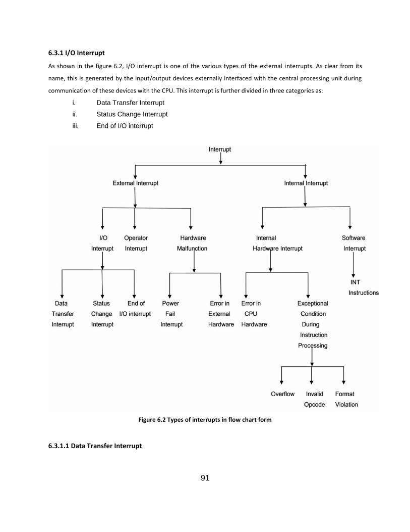
91
6.3.1 I/O Interrupt
As shown in the figure 6.2, I/O interrupt is one of the various types of the external interrupts. As clear from its
name, this is generated by the input/output devices externally interfaced with the central processing unit during
communication of these devices with the CPU. This interrupt is further divided in three categories as:
i. Data Transfer Interrupt
ii. Status Change Interrupt
iii. End of I/O interrupt
Figure 6.2 Types of interrupts in flow chart form
6.3.1.1 Data Transfer Interrupt

92
This is the type of I/O interrupt and generated by I/O controller to inform the CPU that it want to send to or accept
data from CPU. READ command generates the interrupt, to show the readiness of the Input devices to write data
to the CPU. On other hand WRITE command generates the interrupt that shows the readiness of the output device
to accept data from the CPU.
6.3.1.2 Status Change Interrupt
Whenever there is change of the status of any input or the output device, this interrupt is generated. As an
example if any I/O device changes its condition from “READY” status to the “NON-READY” status, then the I/O
controller generates this interrupt to inform the CPU about this status change of the device.
6.3.1.3 End of I/O Interrupt
I/O controller generates “End of I/O Interrupt” whenever any of the I/O device (interfaced with the CPU) operation
is completed. This interrupt can be generated due to any of the following two operations:
a. either on successful completion of an I/O operation,
b. or on stop of I/O operation due to malfunction of the device.
On generation of this interrupt CPU run its interrupt service routine (ISR) to confirm the midway stopping
of the I/O device operation so that the same can be started by the device again.
6.3.2 Operator Interrupt
It is a special type of interrupt to the operating system of the CPU to perform some specific tasks.
6.3.3 Hardware Malfunction Interrupt
Generation of this interrupt is further subdivided in the two categories as:
a. Error in the external hardware
b. Power fail interrupt
6.3.3.1 Error in the External Hardware
Whenever there is a failure or malfunctioning in the operation of the external hardware devices such as memory,
external bus buffers, lathes etc. or the bus structure via which memory or other devices are interfaced with the
CPU, then this interrupt is generated. Most of the times this type of interrupt is treated as non-maskable interrupt
by the processor.
Non – Maskable Interrupt (NMI) is that interrupt which can never be ignored by the processor. These types of the
interrupts are having the highest interrupt priority as compared to the other maskable interrupts. “RESET” is also
93
an example of non maskable interrupt i.e. the system (CPU) resets itself to its default values whenever the RESET is
processed, irrespective of whatever function the CPU is executing at that time.
6.3.3.2 Power Fail Interrupt
This interrupt is generated by a specially designed hardware circuit for the continuous monitoring of fluctuations in
the mains (AC) power. Sudden cut – in or failure in the input ac power supply, this interrupt is generated and its ISR
(interrupt service routine) is executed to save the current status of the CPU in the battery backed memory or
sometimes to switch the operation of a stand - by power supply.
6.3.4 System Management Interrupt
The system management interrupt (SMI) is a special interrupt that manages for the minimum power consumption
by the various external peripheral devices. By using this interrupt CPU continuously monitors the status of the
external devices and it runs an interrupt service routine to power off the device which is not active since long time.
Further they are powered on when ever these devices want any access. The power of time of any external system
can be adjusted by the programmer by specifying its value in the program written for it.
6.4 Internal Interrupts
Internal interrupts are the interrupts that are generated by the internal hardware or the software system of the
central processing unit (CPU) and are subdivided into:
i. Internal Hardware Interrupt
ii. Software Interrupt
6.4.1 Internal Hardware Interrupts
As discussed, these type of interrupts occur due to the errors in the functioning of internal CPU hardware or the
exceptional conditions occur during the instruction processing such as overflow i.e. execution of the operation
generates result of more number of bits than the internal registers can save it. For example result of two 8 bit
numbers can be more than 8 bits which accumulator (an eight bit register internal in the CPU which saves the
result, after the operation is over) is unable to save into it. We have studied in previous chapters the hardware
implementation of the instructions, thus invalid instruction operation code (OPCODE) and illegal instruction format
also generates this interrupt.
6.4.2 Software Interrupts
Software interrupt can be treated as a special CALL instruction that acts as an interrupt irrespective of a
subroutine. Software interrupts are generated by the software instructions written in the program. Sometimes
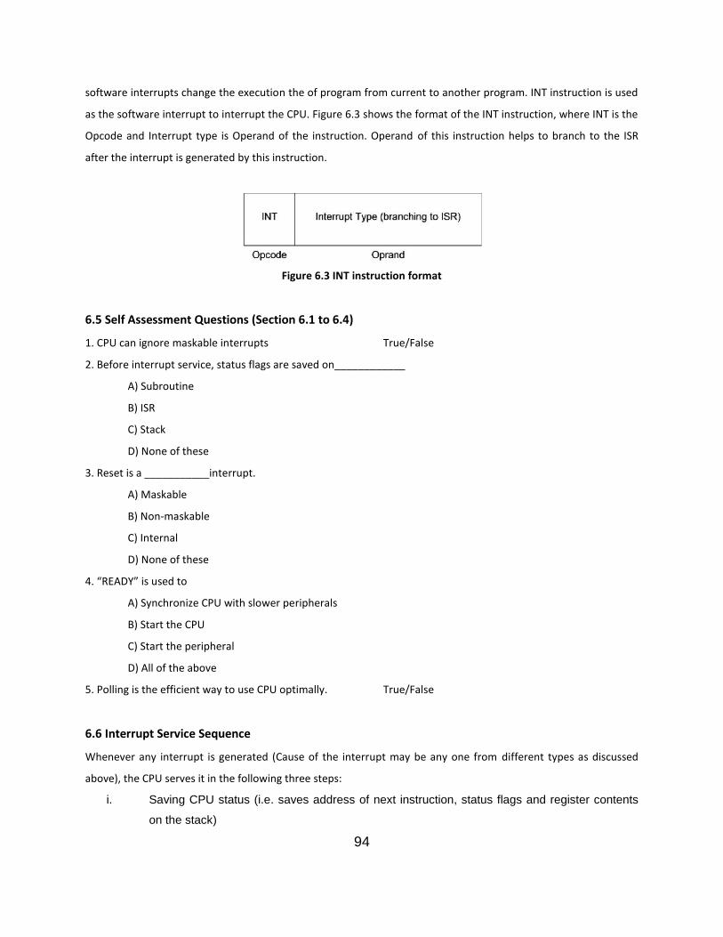
94
software interrupts change the execution the of program from current to another program. INT instruction is used
as the software interrupt to interrupt the CPU. Figure 6.3 shows the format of the INT instruction, where INT is the
Opcode and Interrupt type is Operand of the instruction. Operand of this instruction helps to branch to the ISR
after the interrupt is generated by this instruction.
Figure 6.3 INT instruction format
6.5 Self Assessment Questions (Section 6.1 to 6.4)
1. CPU can ignore maskable interrupts True/False
2. Before interrupt service, status flags are saved on____________
A) Subroutine
B) ISR
C) Stack
D) None of these
3. Reset is a ___________interrupt.
A) Maskable
B) Non-maskable
C) Internal
D) None of these
4. “READY” is used to
A) Synchronize CPU with slower peripherals
B) Start the CPU
C) Start the peripheral
D) All of the above
5. Polling is the efficient way to use CPU optimally. True/False
6.6 Interrupt Service Sequence
Whenever any interrupt is generated (Cause of the interrupt may be any one from different types as discussed
above), the CPU serves it in the following three steps:
i. Saving CPU status (i.e. saves address of next instruction, status flags and register contents
on the stack)
95
ii. Loads PC with address of the source of the interrupt from the vector table.
iii. Starts execution of program written at ISR
The above three steps, in detail are shown in the figure 6.4 in the form of flow chart. Steps in the flow
chart show the sequence of execution of a program while interrupt is enabled by the EI instruction.
Whenever any interrupt is generated by internal or external cause, CPU saves its current status and
status flags, then saves address of the next instruction (i.e. contents of PC) onto the stack, then loads
address of the interrupt from the vector table into the PC, then CPU disables further generation of any
interrupt by executing the instruction DI, then CPU starts execution of program on ISR. When last
instruction (RETI) of ISR is executed, then before loading address of next instruction from stack (where it
was interrupted) into the PC, it enables interrupts by executing instruction EI and again starts execution of
the instruction next to instruction where interrupt was generated in the main program.
6.7 Interrupt CycleThe process of implementation of the hardware to branch to ISR and before it, to save the return address onto the
stack is called the interrupt cycle. The saving of the return address to the safer place/memory (stack) is very
important task of the CPU as it have to start the execution of the instructions (program) again from where the CPU
left to branch to the ISR, failing which error will occur and the system will malfunction. Figure 6.4 shows the
sequence of events during the interrupt cycle. The figure 6.5 shows the flow chart for the interrupt cycle. It shows
the way of interrupt handling by the CPU. In figure 6.5, “R” is called an interrupt flag. The R flip flop decides that
whether CPU will run instruction cycle or the interrupt cycle. When R=0 it means there is no interrupt and the CPU
continuous to execute a routine program (main program). This is called the instruction cycle (when R=0). Before
the start of execution of the instruction cycle, the CPU checks the IEN (sometimes denoted as EI) bit, if interrupt
enable (IEN) bit is reset i.e. IEN=0, it means the programmer has not initialized the interrupts and does not want
the access
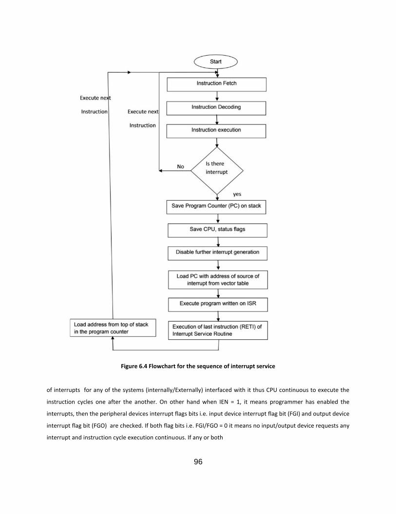
96
Figure 6.4 Flowchart for the sequence of interrupt service
of interrupts for any of the systems (internally/Externally) interfaced with it thus CPU continuous to execute the
instruction cycles one after the another. On other hand when IEN = 1, it means programmer has enabled the
interrupts, then the peripheral devices interrupt flags bits i.e. input device interrupt flag bit (FGI) and output device
interrupt flag bit (FGO) are checked. If both flag bits i.e. FGI/FGO = 0 it means no input/output device requests any
interrupt and instruction cycle execution continuous. If any or both
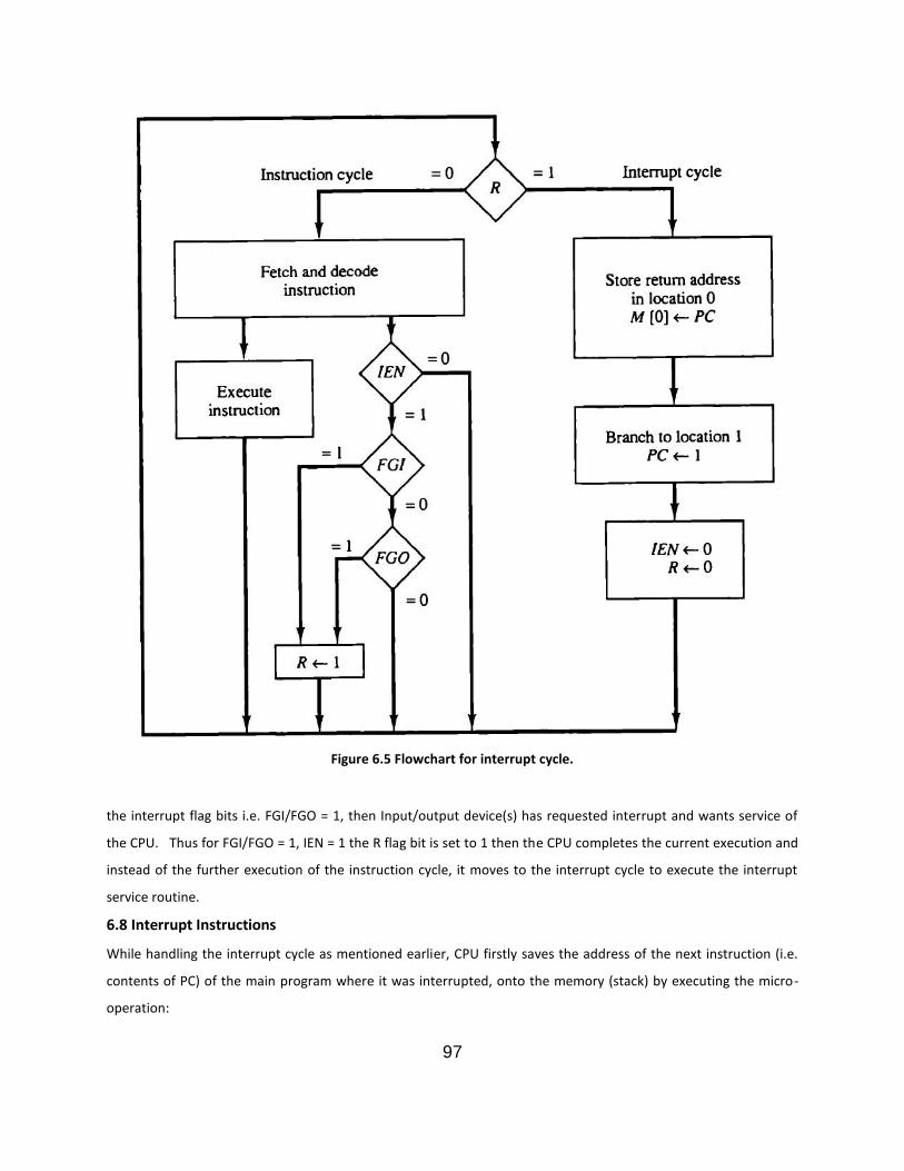
97
Figure 6.5 Flowchart for interrupt cycle.
the interrupt flag bits i.e. FGI/FGO = 1, then Input/output device(s) has requested interrupt and wants service of
the CPU. Thus for FGI/FGO = 1, IEN = 1 the R flag bit is set to 1 then the CPU completes the current execution and
instead of the further execution of the instruction cycle, it moves to the interrupt cycle to execute the interrupt
service routine.
6.8 Interrupt Instructions
While handling the interrupt cycle as mentioned earlier, CPU firstly saves the address of the next instruction (i.e.
contents of PC) of the main program where it was interrupted, onto the memory (stack) by executing the micro-
operation:
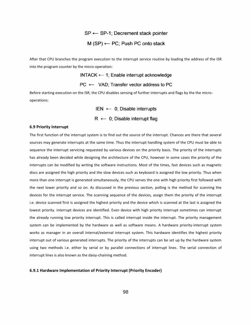
98
After that CPU branches the program execution to the interrupt service routine by loading the address of the ISR
into the program counter by the micro-operation:
Before starting execution on the ISR, the CPU disables sensing of further interrupts and flags by the the micro-
operations:
6.9 Priority Interrupt
The first function of the interrupt system is to find out the source of the interrupt. Chances are there that several
sources may generate interrupts at the same time. Thus the interrupt handling system of the CPU must be able to
sequence the interrupt servicing requested by various devices on the priority basis. The priority of the interrupts
has already been decided while designing the architecture of the CPU, however in some cases the priority of the
interrupts can be modified by writing the software instructions. Most of the times, fast devices such as magnetic
discs are assigned the high priority and the slow devices such as keyboard is assigned the low priority. Thus when
more than one interrupt is generated simultaneously, the CPU serves the one with high priority first followed with
the next lower priority and so on. As discussed in the previous section, polling is the method for scanning the
devices for the interrupt service. The scanning sequence of the devices, assign them the priority of the interrupt
i.e. device scanned first is assigned the highest priority and the device which is scanned at the last is assigned the
lowest priority. interrupt devices are identified. Even device with high priority interrupt sometimes can interrupt
the already running low priority interrupt. This is called interrupt inside the interrupt. The priority management
system can be implemented by the hardware as well as software means. A hardware priority-interrupt system
works as manager in an overall Internal/external interrupt system. This hardware identifies the highest priority
interrupt out of various generated interrupts. The priority of the interrupts can be set up by the hardware system
using two methods i.e. either by serial or by parallel connections of interrupt lines. The serial connection of
interrupt lines is also known as the daisy-chaining method.
6.9.1 Hardware Implementation of Priority Interrupt (Priority Encoder)
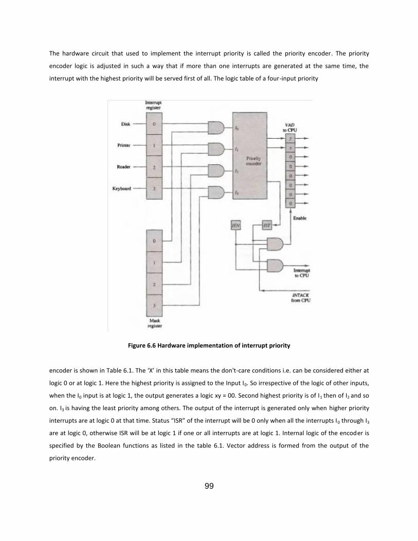
99
The hardware circuit that used to implement the interrupt priority is called the priority encoder. The priority
encoder logic is adjusted in such a way that if more than one interrupts are generated at the same time, the
interrupt with the highest priority will be served first of all. The logic table of a four-input priority
Figure 6.6 Hardware implementation of interrupt priority
encoder is shown in Table 6.1. The ‘X’ in this table means the don't-care conditions i.e. can be considered either at
logic 0 or at logic 1. Here the highest priority is assigned to the Input I0. So irrespective of the logic of other inputs,
when the I0 input is at logic 1, the output generates a logic xy = 00. Second highest priority is of I1 then of I2 and so
on. I3 is having the least priority among others. The output of the interrupt is generated only when higher priority
interrupts are at logic 0 at that time. Status “ISR” of the interrupt will be 0 only when all the interrupts I0 through I3
are at logic 0, otherwise ISR will be at logic 1 if one or all interrupts are at logic 1. Internal logic of the encoder is
specified by the Boolean functions as listed in the table 6.1. Vector address is formed from the output of the
priority encoder.

100
Table 6.1 Truth Table for Priority Encoder
6.10 Example of Interrupt Program
CPU wastes its precious time in waiting for the external I/O device till its flag sets to logic 1. Monitoring of flags in
various loops also consumes time of the CPU. The efficient method for optimally using the time of
Table 6.2 Program for service of interrupt
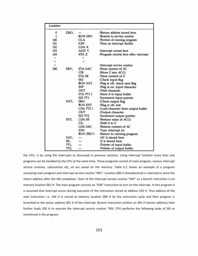
101
the CPU, is by using the interrupts as discussed in previous sections. Using interrupt function more than one
programs can be handled by the CPU at the same time. These programs consist of main program, various interrupt
service routines, subroutines etc, all are saved on the memory. Table 6.2 shows an example of a program
consisting main program and interrupt service routine “SRV”. Location 000 H (hexadecimal) is reserved to store the
return address after the ISR completion. Start of the Interrupt service routine “SRV” as a branch instruction is on
memory location 001 H. The main program consists an “ION” instruction to turn on the interrupt. In this program it
is assumed that interrupt occurs during execution of the instruction stored at address 103 H. Thus address of the
next instruction i.e. 104 H is stored at memory location 000 H by the instruction cycle and then program is
branched to the vector address 001 H of the interrupt. Branch instruction written on 001 H (vector address) then
further loads 200 H to execute the interrupt service routine “SRV. CPU performs the following tasks of ISR as
mentioned in the program:
102
6.11 Self Assessment Questions (Section 6.6 to 6.10)1. Interrupts which are initiated by an instruction are ............
A) internal
B) external
C) hardware
D) software
2. When the CPU detects an interrupt, it then saves its ...................
A) Previous state
B) Next state
C) Current state
D) Both A and B
3. An exception conditions in a computer system by an event external to the CPU is called .........
A) Interrupt
B) halt
C) wait
D) process
4. ________establishes a interrupt priority over the various sources to determine which request should be
entertained first:
A). Priority interrupt
B). Polling
C) Daisy chaining
D) None of these
5. The interrupt-request line is a part of the
A) Data line
B) Control line
C) Address line
D) None
6. Interrupts form an important part of _____ systems
103
A) Batch processing
B) Multitasking
C) Real-time processing
D) Multi-user
6.12 Summary
Writing programs using interrupts is the efficient way of programming for optimal functioning of the CPU.
Interrupt means CPU stops current execution of commands to give priority to perform some other task requested
by the external or the internal device. Interrupts can be divided in various categories as:
External Interrupts: generated by the external hardware devices such as input/output devices
interfaced with the CPU when they have to communicate with the CPU.
Internal Interrupts: generated by the internal hardware of the CPU or the software commands
such as INT.
Interrupt cycle is the process of implementation of the hardware for running the Interrupt Service
Routine.
Non-Maskable interrupts are immediately handled by the CPU and it can never ignore these.
Maskable interrupts are handled by the CPU as per their priority
Higher priority interrupt can midway interrupt the running lower priority interrupt. This is called
interrupt inside interrupt.
IEN = 1 enables the interrupts
INTACK (Interrupt Acknowledge) is used to confirm the interrupt to the peripheral device.
To enable interrupt is the duty of the programmer.
Before execution of the ISR further interrupts are disabled by the CPU.
After the ISR has finished, CPU starts execution again in the main program from where it had left
for serving ISR.
6.13 Glossary
INT – Interrupt.
INTR – Interrupt Request.
INTA – Interrupt Acknowledge.
ISR – Interrupt Service Routine.
NMI– Non Maskable Interrupt
I/O – Input/Output
SMI – System Management Interrupt
IRQ – Interrupt Request
104
RETI – Return from interrupt
EI – Enable Interrupt
DI – Disable Interrupt.
IF – Interrupt Flag.
IP – Interrupt Priority.
DMA – Direct Memory Access.
DRQ – Device Controller Request.
BAL – Bus Arbitration Logic
BR – Bus Request
PIC – Programmable Interrupt Controller
6.14 Answers of Self Assessment Questionsa. Section 6.1 to 6.4
14. D
15. B
16. A
17. B
18. D
19. B
b.Section 6.6 to 6.101. True
2. C
3. B
4. A
5. False
6.15 Bibliography/References/Suggested Readings
13. Computer System Architecture by M. Morris Mano, Pearson Publication.
14. Computer Architecture and Organization (Design Principles and Applications) by B Govindarajalu, McGraw
Hill.
15. Computer Architecture and Organization by J.P. Hays, Tata McGraw-Hill Publishing.
16. Computer Architecture: A Quantitative Approach. J. L. Hennessy and D. A. Patterson Morgan Kaufmann,
San Francisco, CA, fifth edition
17. Computer Organization and Architecture by William Stallings, Pearson Publication
18. Computer Organization and Design, Pal Choudhary, PHI

105
19. www.nptel.iitm.ac.in
6.16 Terminal and Model Questions
1. Give five examples of each external as well as internal interrupts. Differentiate software interrupt and a
subroutine call.
2. A computer responds to an interrupt request signal by pushing onto the stack the contents of PC and the current
PSW (program status word). It then reads a new PSW from memory from a location given by an interrupt address
symbolized by IAD. The first address of the service program is taken from memory at location IAD + 1.
a. List the sequence of micro-operations for the interrupt cycle.
b. List the sequence of micro-operations for the return from interrupt instruction.
3. Differentiate interrupt vs polling.
4. Name various flags used in the interrupts. Explain their roll in handling the interrupts by the CPU.
5. What do you mean by interrupt priority?
6. Is it possible to serve the lower priority maskable interrupt before the higher priority interrupt?
7. What is the difference in subroutine and interrupt service routine?
8. Write the steps that the CPU follows to serve an interrupt.
106
Lesson 7
Design of Control Unit
Structure
7.0 Objectives
7.1 Introduction
7.2 Control Unit
7.3 Hardwired Control Unit
7.4 Microprogrammed Control Unit
7.5 Difference between hardwired and microprogrammed control unit
7.6 Summary
7.7 Glossary
7.8 Answer to Check Your Progress/Suggested Answers to SAQ
7.9 Bibliography/References/ Suggested Readings
7.10 Terminal and Model Questions
7.0 Objectives
After studying this chapter you will understand
The basic of Control Unit
Hardwired Control Unit
Microprogrammed Control Unit
Microinstructions concept.
Control Memory
Microprogram
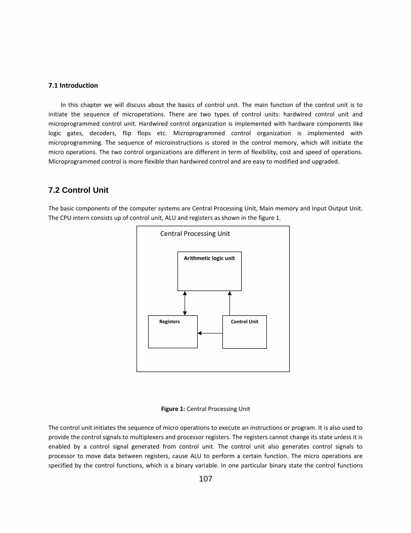
107
7.1 Introduction
In this chapter we will discuss about the basics of control unit. The main function of the control unit is toinitiate the sequence of microperations. There are two types of control units: hardwired control unit andmicroprogrammed control unit. Hardwired control organization is implemented with hardware components likelogic gates, decoders, flip flops etc. Microprogrammed control organization is implemented withmicroprogramming. The sequence of microinstructions is stored in the control memory, which will initiate themicro operations. The two control organizations are different in term of flexibility, cost and speed of operations.Microprogrammed control is more flexible than hardwired control and are easy to modified and upgraded.
7.2 Control Unit
The basic components of the computer systems are Central Processing Unit, Main memory and Input Output Unit.The CPU intern consists up of control unit, ALU and registers as shown in the figure 1.
Figure 1: Central Processing Unit
The control unit initiates the sequence of micro operations to execute an instructions or program. It is also used toprovide the control signals to multiplexers and processor registers. The registers cannot change its state unless it isenabled by a control signal generated from control unit. The control unit also generates control signals toprocessor to move data between registers, cause ALU to perform a certain function. The micro operations arespecified by the control functions, which is a binary variable. In one particular binary state the control functions
Central Processing Unit
Arithmetic logic unit
Registers Control Unit
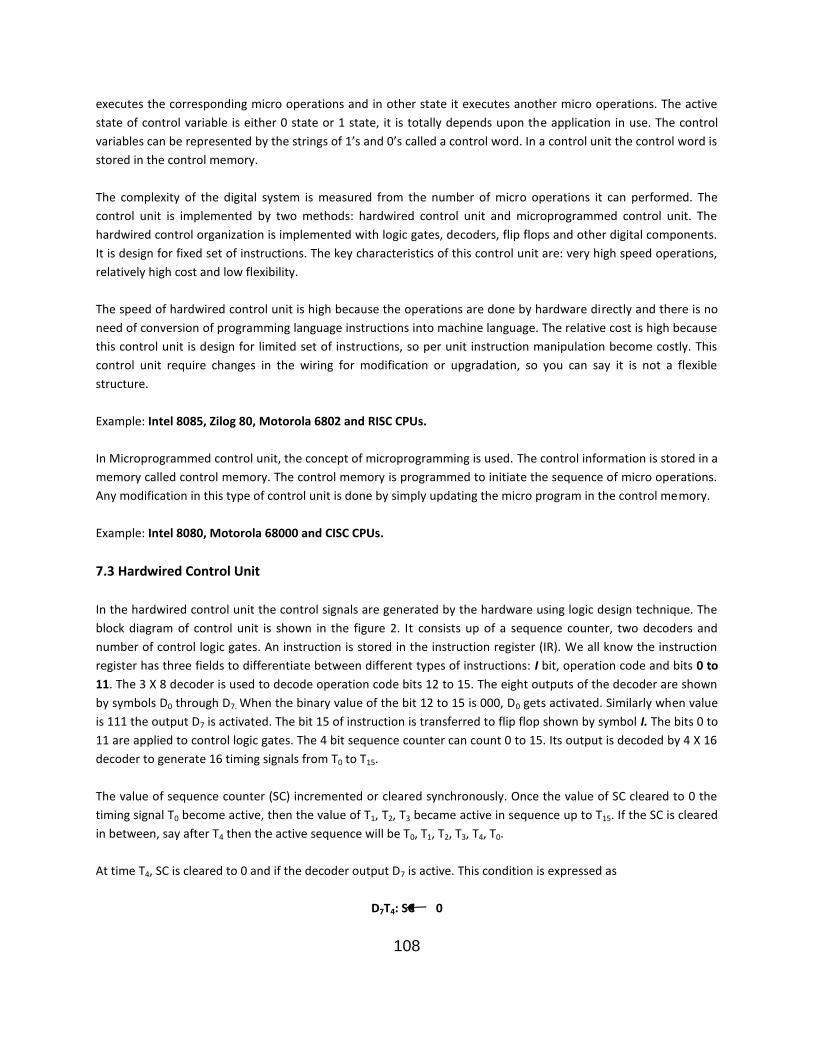
108
executes the corresponding micro operations and in other state it executes another micro operations. The activestate of control variable is either 0 state or 1 state, it is totally depends upon the application in use. The controlvariables can be represented by the strings of 1’s and 0’s called a control word. In a control unit the control word isstored in the control memory.
The complexity of the digital system is measured from the number of micro operations it can performed. Thecontrol unit is implemented by two methods: hardwired control unit and microprogrammed control unit. Thehardwired control organization is implemented with logic gates, decoders, flip flops and other digital components.It is design for fixed set of instructions. The key characteristics of this control unit are: very high speed operations,relatively high cost and low flexibility.
The speed of hardwired control unit is high because the operations are done by hardware directly and there is noneed of conversion of programming language instructions into machine language. The relative cost is high becausethis control unit is design for limited set of instructions, so per unit instruction manipulation become costly. Thiscontrol unit require changes in the wiring for modification or upgradation, so you can say it is not a flexiblestructure.
Example: Intel 8085, Zilog 80, Motorola 6802 and RISC CPUs.
In Microprogrammed control unit, the concept of microprogramming is used. The control information is stored in amemory called control memory. The control memory is programmed to initiate the sequence of micro operations.Any modification in this type of control unit is done by simply updating the micro program in the control memory.
Example: Intel 8080, Motorola 68000 and CISC CPUs.
7.3 Hardwired Control Unit
In the hardwired control unit the control signals are generated by the hardware using logic design technique. Theblock diagram of control unit is shown in the figure 2. It consists up of a sequence counter, two decoders andnumber of control logic gates. An instruction is stored in the instruction register (IR). We all know the instructionregister has three fields to differentiate between different types of instructions: I bit, operation code and bits 0 to11. The 3 X 8 decoder is used to decode operation code bits 12 to 15. The eight outputs of the decoder are shownby symbols D0 through D7. When the binary value of the bit 12 to 15 is 000, D0 gets activated. Similarly when valueis 111 the output D7 is activated. The bit 15 of instruction is transferred to flip flop shown by symbol I. The bits 0 to11 are applied to control logic gates. The 4 bit sequence counter can count 0 to 15. Its output is decoded by 4 X 16decoder to generate 16 timing signals from T0 to T15.
The value of sequence counter (SC) incremented or cleared synchronously. Once the value of SC cleared to 0 thetiming signal T0 become active, then the value of T1, T2, T3 became active in sequence up to T15. If the SC is clearedin between, say after T4 then the active sequence will be T0, T1, T2, T3, T4, T0.
At time T4, SC is cleared to 0 and if the decoder output D7 is active. This condition is expressed as
D7T4: SC 0
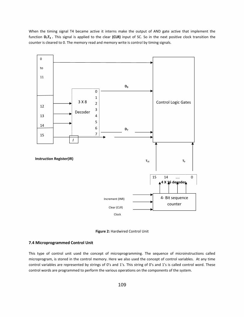
109
Increment (INR)
When the timing signal T4 became active it interns make the output of AND gate active that implement thefunction D7T4 . This signal is applied to the clear (CLR) input of SC. So in the next positive clock transition thecounter is cleared to 0. The memory read and memory write is control by timing signals.
Instruction Register(IR)
Figure 2: Hardwired Control Unit
7.4 Microprogrammed Control Unit
This type of control unit used the concept of microprogramming. The sequence of microinstructions calledmicroprogram, is stored in the control memory. Here we also used the concept of control variables. At any timecontrol variables are represented by strings of 0’s and 1’s. This string of 0’s and 1’s is called control word. Thesecontrol words are programmed to perform the various operations on the components of the system.
3 X 8
Decoder
01234567
15 14 .... 04 X 16 decoder
I
0
to
11
12
13
14
15
Control Logic Gates
4- Bit sequencecounter
Clear (CLR)
Clock
D0
D7
T15 T0

110
The control memory is read only memory (ROM) i.e. its contents are fixed and cannot be changed when thecontrol unit is in function. The ROM words are made permanent during the hardware production. The contents ofword of control memory at a particular address specify the microinstruction.
The more advance control unit use dynamic microprogramming. This type of control unit employs the writablecontrol memory. The computer systems with microprogrammed control unit have two types of memories: a mainmemory and a control memory. The main memory is used to store the programs and its contents get altered whenthe data is manipulated. The user programs in this memory are consists up of machine instructions and data. Butthe content of control memory is fixed and cannot be altered by occasional user. Each machine instructionsinitiates the series of microinstructions in the control memory. The microinstructions initiate the following set ofmicrooperations:
Fetch an instruction from the main memory. Evaluate the effective address of data. Execute the operation specified by the instructions. Return to fetch phase to repeat the cycle again
The block diagram of microprogrammed control unit is shown in figure 3
External input
Next address information
Control word
Figure 3: Microprogrammed Control Unit
Sequencer: It is also called next address generator. The task of this block is to generate the next address. Theaddress of next microinstruction may in the sequence of previous instruction or somewhere else in the controlmemory. So some bits of present address may be used for generation of next address. The next address may bethe function of some external input during microoperation is being executed. Next address generated istransferred to control address register.
Control Address Register: Control memory address register specifies the address of the microinstruction that isbeing executed. Typically the sequencer increment the control address register by one.
Control Memory: It is used to store the control information permanently. It is assumed to be ROM.
Sequencer
Control dataregister
Controlmemory
Controladdressregister
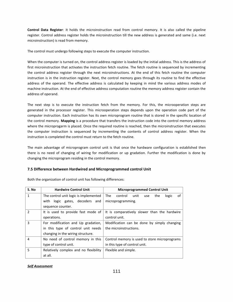
111
Control Data Register: It holds the microinstruction read from control memory. It is also called the pipelineregister. Control address register holds the microinstruction till the new address is generated and same (i.e. nextmicroinstruction) is read from memory.
The control must undergo following steps to execute the computer instruction.
When the computer is turned on, the control address register is loaded by the initial address. This is the address offirst microinstruction that activates the instruction fetch routine. The fetch routine is sequenced by incrementingthe control address register through the next microinstructions. At the end of this fetch routine the computerinstruction is in the instruction register. Next, the control memory goes through its routine to find the effectiveaddress of the operand. The effective address is calculated by keeping in mind the various address modes ofmachine instruction. At the end of effective address computation routine the memory address register contain theaddress of operand.
The next step is to execute the instruction fetch from the memory. For this, the microoperation steps aregenerated in the processor register. This microoperation steps depends upon the operation code part of thecomputer instruction. Each instruction has its own microprogram routine that is stored in the specific location ofthe control memory. Mapping is a procedure that transfers the instruction code into the control memory addresswhere the microprogarm is placed. Once the required routine is reached, then the microinstruction that executesthe computer instruction is sequenced by incrementing the contents of control address register. When theinstruction is completed the control must return to the fetch routine.
The main advantage of microprogram control unit is that once the hardware configuration is established thenthere is no need of changing of wiring for modification or up gradation. Further the modification is done bychanging the microprogram residing in the control memory.
7.5 Difference between Hardwired and Microprogrammed control Unit
Both the organization of control unit has following differences:
S. No Hardwire Control Unit Microprogrammed Control Unit1 The control unit logic is implemented
with logic gates, decoders andsequence counter.
The control unit use the logic ofmicroprogramming.
2 It is used to provide fast mode ofoperations.
It is comparatively slower than the hardwirecontrol unit.
3 For modification and Up gradation,in this type of control unit needschanging in the wiring structure.
Modification can be done by simply changingthe microinstructions.
4 No need of control memory in thistype of control unit.
Control memory is used to store microprogramsin this type of control unit.
5 Relatively complex and no flexibilityat all.
Flexible and simple.
Self Assessment
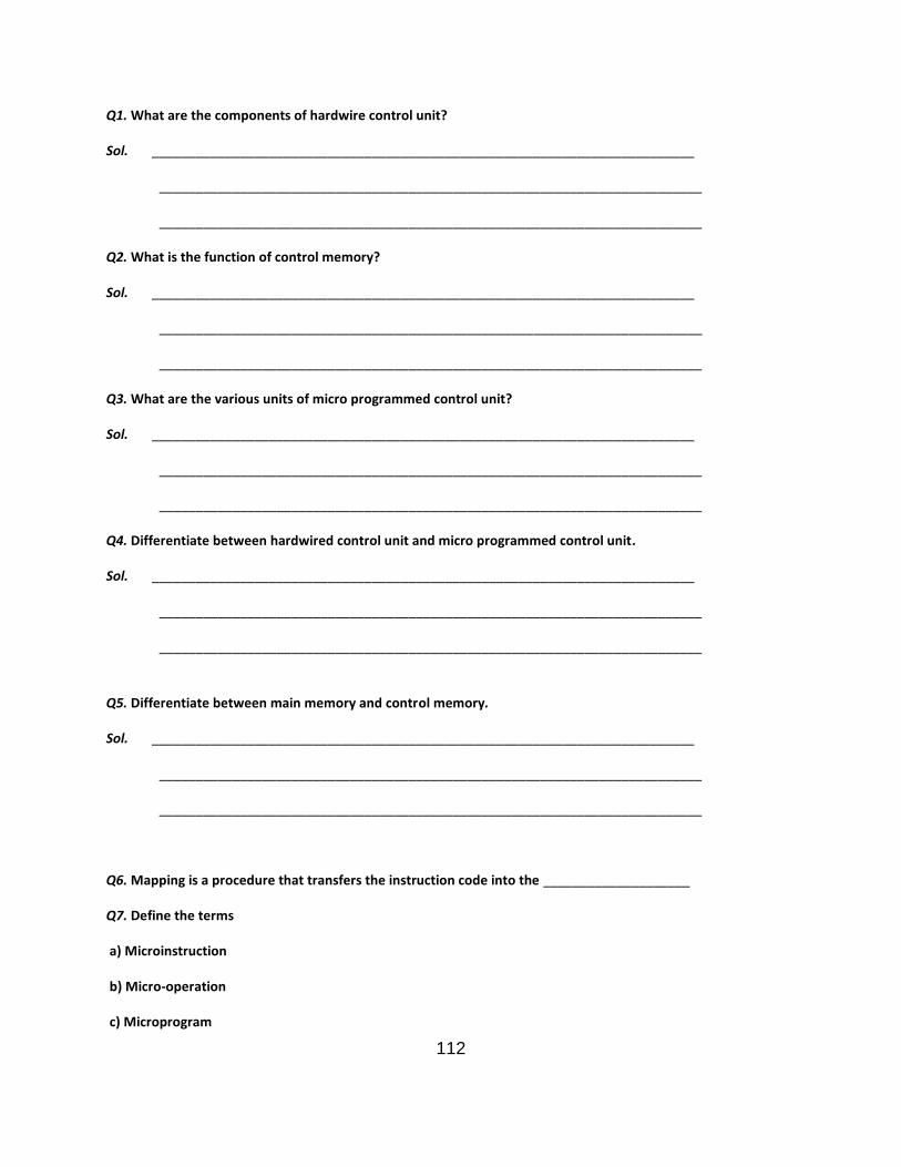
112
Q1. What are the components of hardwire control unit?
Sol. __________________________________________________________________________
__________________________________________________________________________
__________________________________________________________________________
Q2. What is the function of control memory?
Sol. __________________________________________________________________________
__________________________________________________________________________
__________________________________________________________________________
Q3. What are the various units of micro programmed control unit?
Sol. __________________________________________________________________________
__________________________________________________________________________
__________________________________________________________________________
Q4. Differentiate between hardwired control unit and micro programmed control unit.
Sol. __________________________________________________________________________
__________________________________________________________________________
__________________________________________________________________________
Q5. Differentiate between main memory and control memory.
Sol. __________________________________________________________________________
__________________________________________________________________________
__________________________________________________________________________
Q6. Mapping is a procedure that transfers the instruction code into the ____________________
Q7. Define the terms
a) Microinstruction
b) Micro-operation
c) Microprogram
113
7.6 Summary
The Central Processing Unit (CPU) is the major functional part of computer system. The CPU is further consisting upof ALU, Registers and Control Unit. The control unit coordinates all the activities of system. It initiates thesequence of microoperations to execute the computer instructions. The two designs of control unit are HardwiredControl Unit and Microprogrammed Control Unit. The key characteristics of hardwired control unit are high speed,costly, more complex and no flexibility. It consist of hardware components like decoders, flip flops, logic gates etc.further its works for fixed set of instruction set. If we want to upgrade the hardwired control unit then we need tochange the complete wiring set up.
The other type of control unit is the microprogrammed control unit. The main components of this type of controlunits are sequencer, control address register, control memory and control data register. The microinstructions arestored in the control memory. These microinstructions are consisting up of control word. The set ofmicroinstructions constitutes the microprogram. The sequencer are also called next address generator. Theoperation of sequencer is to generator the address of next microinstruction that is to read from the controlmemory. The task of up gradation is easy in the microprogrammed control unit as it use the concept ofmicroprogramming and control memory.
7.7 Glossary
Control Address Register: CAR stores the address of microinstructions in microprogrammed control unit. Control Data Register: It holds the microinstruction reads from the control memory. Control function: It specifies a microinstruction is a binary variable. Depending upon its state
microoperations is executed. Control memory: A memory of control unit is called control memory. Control unit: It is a part of CPU. The main function of control unit is to initiates the sequence of
microoperations Microinstruction: Microinstructions are the control words that are stored in the
control memory. Microprogram: Sequence of microinstructions constitutes the microprogram. Operation code: The operation code of the instruction specifies the operation to be performed. It is also
called opcode. Sequencer: It is also called next address generator. It generates the address sequence read from the
control memory.
7.8 Answer to Check Your Progress/Suggested Answers to SAQ
Self Assessment
Solution 1) The hardwired control unit consist up of:Decoders: 3 X 8 decoder, 4 X 16 decoderControl logic gatesFlip-flopsSequence counter
114
.Solution 2) Control memory is an integral part of control unit. It is work both in write and read mode it
stores the sequence of microinstructions. These microinstructions initiate the microoperations for the execution of computer instructions.
Solution 3) The various blocks of micro programmed control unit are:SequencerControl Address RegisterControl MemoryControl Data Register
Solution 4) See section 7.5
Solution 5) Main memory is used to store the computer programs and its contents get altered whenthe data is manipulated. The user programs in this memory are consists up of machineinstructions and data. But the content of control memory is fixed and cannot be altered by
occasional user
Solution 6) Control memory address
Solution 7) a) Microinstructions: Microinstructions are the control words that are stored in thecontrol memory. It specifies one or more microoperations for the computer systems.
b) Microoperations: Microoperations are the series of steps used by control unit toexecute the computer instructions. It initiate the operations such as instruction fetch,data read and instruction execute.
c) Microprogram: Sequence of microinstructions constitutes the microprogram.Contents of microprogram are fixed and stored in the control memory.
7.9 Bibliography/References/ Suggested Readings
1. Computer System Architecture, M.M. Mano, Third Edition, PHI2. Computer Organization and Architecture Lab.3. Computer Organization and Architecture, Stallings, Eighth Edition, PHI
7.10 Terminal and Model Questions
Q1. What is function of control unit?
Q2. Explain how the mapping from an instruction code to a microinstruction is done by read onlymemory.
Q3. Explain by microprogrammed control unit is better than hardwired control unit in term of flexibility
Q4. Differentiate between microprocessor and microprogram.

115
Q5. Explain the hardwired wired control unit with its block diagram?
Q6. Explain the microprogrammed control unit with its block diagram.

116
Lesson 8
Addressing Modes
Structure8.0 Objectives
8.1 Introduction
8.2 Instruction Cycle
8.2.1 Instruction Fetch Cycle
8.2.2 Instruction Decoding
8.2.3 Instruction Execution
8.3 Addressing Modes
8.4 Self Assessment Questions (Section 8.1 to 8.3)
8.5 Instruction Format
8.5.1 Three-Address Instructions
8.5.2 Two-Address Instructions
8.5.3 One-Address Instructions
8.5.4 Zero-Address Instructions
8.6 Self Assessment Questions (Section 8.5)
8.7 Type of Addressing Modes
8.7.1 Implied Addressing Mode
8.7.2 Immediate Addressing Mode
8.7.3 Register Addressing Mode
8.7.4 Register Indirect Addressing Mode
8.7.5 Auto-increment or Auto-decrement Addressing Mode
8.7.6 Direct Addressing Mode
8.7.7 Indirect Addressing Mode
8.7.8 Relative Addressing Mode
8.7.9 Indexed Addressing Mode
8.7.10 Base Register Addressing Mode
8.8 Self Assessment Questions (Section 8.7)
8.9 Summary
8.10 Glossary
8.11 Answers to check your progress/Suggested Answers to Questions
117
8.12 Bibliography/References/Suggested Readings
8.13 Terminal and Model Questions
8.0 Objectives
Objectives of learning the concept of the addressing modes are:
Concept of instruction cycle
To understand the instruction format
Study the of parts of an instruction
Classification of instructions based on the address fields of an operand
Study of zero through three address field instructions
Concept of addressing modes
Study of different type of addressing modes

118
After the completion of this chapter students will be able to understand the basic concepts of instruction cycle,
instruction format and classification of instructions based on the address fields of an operand. Understanding the
concept of addressing modes will help them to proceed for writing various programs in the efficient way by using
lesser number of instructions that takes less space on memory and even less time for execution.
8.1 Introduction
The instructions we have studied till now can be divided in the two parts i.e. OPCODE (operation code) and
OPERAND. Opcode defines the operation/function to be performed and operand is the part of the instruction on
which operation is performed. The operand is the data stored in the registers, memory or it can be the immediate
data. The type of the operand (registers, memory, I/O ports or the immediate data) is defined by the addressing
modes of the instruction or in other terms various formats that expresses the operands is called the addressing
modes. The addressing mode does not mean that address of every operand is defined in the instruction; it decides
that how fast the instruction cycle is completed. A CPU may not use all the addressing modes in different programs
it runs. Addressing modes provide the programmers the following facilities (one or both) in writing various
programs:
1. To provide programming variations to the programmer by having the facilities of using memory
pointers, loops for counters control, program relocation and indexing of data.
2. For using less number of bits to address the operand of the instruction i.e. to write program by
using that addressing modes by which minimum number of memory locations be required to
save it.
8.2 Instruction Cycle
Addressing modes availability provides flexibility to the experienced programmers for writing programs in
assembly or other language with the more efficient way (short and fast) in terms of the number of less number of
instructions with the small execution time. For the understanding of the concept of various addressing modes, it is
necessary to understand the basic concept of the instruction cycle execution. Operation cycle of an instruction is
divided in the following sub cycles or operations:
Instruction fetch cycle: Reads Opcode of instruction from the memory.
Instruction decoding.
Instruction execution.
8.2.1 Instruction Fetch Cycle
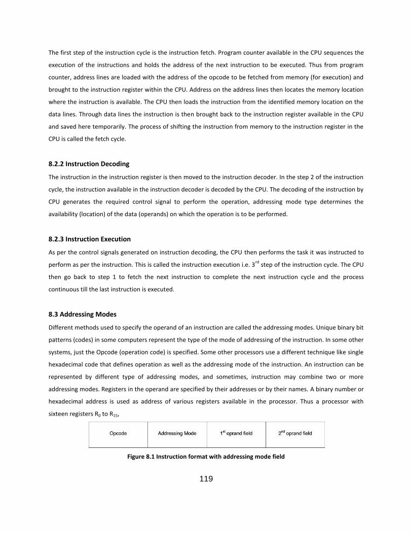
119
The first step of the instruction cycle is the instruction fetch. Program counter available in the CPU sequences the
execution of the instructions and holds the address of the next instruction to be executed. Thus from program
counter, address lines are loaded with the address of the opcode to be fetched from memory (for execution) and
brought to the instruction register within the CPU. Address on the address lines then locates the memory location
where the instruction is available. The CPU then loads the instruction from the identified memory location on the
data lines. Through data lines the instruction is then brought back to the instruction register available in the CPU
and saved here temporarily. The process of shifting the instruction from memory to the instruction register in the
CPU is called the fetch cycle.
8.2.2 Instruction Decoding
The instruction in the instruction register is then moved to the instruction decoder. In the step 2 of the instruction
cycle, the instruction available in the instruction decoder is decoded by the CPU. The decoding of the instruction by
CPU generates the required control signal to perform the operation, addressing mode type determines the
availability (location) of the data (operands) on which the operation is to be performed.
8.2.3 Instruction Execution
As per the control signals generated on instruction decoding, the CPU then performs the task it was instructed to
perform as per the instruction. This is called the instruction execution i.e. 3rd step of the instruction cycle. The CPU
then go back to step 1 to fetch the next instruction to complete the next instruction cycle and the process
continuous till the last instruction is executed.
8.3 Addressing Modes
Different methods used to specify the operand of an instruction are called the addressing modes. Unique binary bit
patterns (codes) in some computers represent the type of the mode of addressing of the instruction. In some other
systems, just the Opcode (operation code) is specified. Some other processors use a different technique like single
hexadecimal code that defines operation as well as the addressing mode of the instruction. An instruction can be
represented by different type of addressing modes, and sometimes, instruction may combine two or more
addressing modes. Registers in the operand are specified by their addresses or by their names. A binary number or
hexadecimal address is used as address of various registers available in the processor. Thus a processor with
sixteen registers R0 to R15,
Figure 8.1 Instruction format with addressing mode field
120
uses address starting from 0000 (R0) to 1111 (R15) to represent registers. For example the binary number 0111,
will represent the register R7. Exact addressing mode used in the instruction is indicated to the control unit in any
of the following two ways:
Addressing mode used by an instruction is indicated by a separate mode field as shown in the
figure 8.1.
Opcode itself (explicit instruction) specifies the used addressing mode in that instruction.
Instructions used in the computers may be of different lengths, with one or more than one number of address
fields. The internal organization of its registers in the instruction decides the number of address fields. The CPU
internal organizations of most of the computers fall into one of the three categories as given below:
1. Single accumulator organization (i.e. one address field instructions).
2. General register organization (i.e. only registers name in the operand).
3. Stack organization (i.e. Address field with PUSH, POP instructions).
The basic computer is an example of an accumulator-type organization. These types of
systems perform operations with a single accumulator register (called implied mode). This type
of instruction format mostly uses one address field.
In a general register type of organization, multiple registers are the part of the operand of the
instruction. These types of systems use two or three address instruction format. Address field
of each instruction, specifies internal register or a memory address.
Computer systems with stack organization would have two instructions such as PUSH and
POP, with a required address field.
8.4 Self Assessment Questions (Section 8.1 to 8.3)
1. Instruction has been divided into two parts called__________and____________
2. During execution of instruction, 1st operation is called_____________
3. Method used to specify the operand of an instruction is called.
A. Instruction decoding
B. Addressing modes
C. Instruction fetch
D. None of these
4. Stack is accessed by using the instructions
A. PUSH
B. JUMP
C. CALL
D. All of above
5. Address of the instruction to be executed is available in ___________ register.
121
8.5 Instruction Format
Before studying in detail the different type of addressing modes, it is must to understand the concept and format
of the instructions. Most of the computer systems use one of the three types of organizations that have just been
explained. Some of the CPU features are the combination of more than one system structures. For example,
internal architecture of the Intel 8085 microprocessor consists of 7 inbuilt registers (B, C, D, E, H, L, A), where A
(accumulator) is called a special purpose register. Thus it is a processor which has characteristics as a combination
of a general register type structure and the features of an accumulator register structure. Logical and arithmetical
instructions and some of the data transfer instructions such as load and store are performed through the
accumulator as one of the operand register. These instructions are the examples of one address field instructions.
In other case, the set of instructions that performs data transfer in between the 8085 µP (microprocessor) internal
registers, are called two address field instructions. General structure of an instruction format as shown in the
figure 8.1, in many cases is represented in a rectangular form. The bits format of an instruction is normally divided
into the groups called instruction fields. Commonly used groups or fields shown in the instruction consist of:
1. Opcode or an operation code: represents the operation performed on the operands.
2. Addressing mode: the way by which the operand or the effective address is determined.
3. Operand field: represents a memory address or a processor’s internal register(s).
Based on the address format most of the instructions can be categorized as:
Three address field instructions.
Two address field instructions
One address field instructions
Zero address field instructions
Explanation of the above types is given as below
8.5.1 Three-Address Instructions
Address field in the three-address instruction format can be specified as the name of a register or as address of
memory as operand. An example that shows an assembly language program to calculates Z = (A + B) * (C + D) is
shown in table 8.1 along with comments in the micro-operations form, that explains the register transfer operation
of each instruction. In this example, processor’s internal registers R1 and R2 are used in these instructions as an
operand. M[A] is the symbol that represents the 1st operand available in the memory. Address of this memory is
pointed by the square bracketed number (letter ‘A’ here). The major advantage of using this three address
instruction format is that, less number of instructions are required for writing programs for performing arithmetic
operations. Drawback of using three address instructions is that the binary-code of the instruction address is too
lengthy as it is to be specified by the more number of bits.
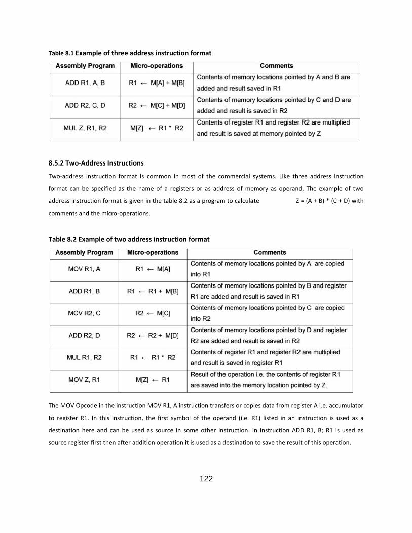
122
Table 8.1 Example of three address instruction format
8.5.2 Two-Address Instructions
Two-address instruction format is common in most of the commercial systems. Like three address instruction
format can be specified as the name of a registers or as address of memory as operand. The example of two
address instruction format is given in the table 8.2 as a program to calculate Z = (A + B) * (C + D) with
comments and the micro-operations.
Table 8.2 Example of two address instruction format
The MOV Opcode in the instruction MOV R1, A instruction transfers or copies data from register A i.e. accumulator
to register R1. In this instruction, the first symbol of the operand (i.e. R1) listed in an instruction is used as a
destination here and can be used as source in some other instruction. In instruction ADD R1, B; R1 is used as
source register first then after addition operation it is used as a destination to save the result of this operation.
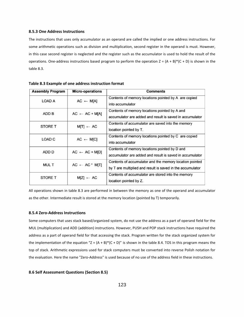
123
8.5.3 One Address Instructions
The instructions that uses only accumulator as an operand are called the implied or one address instructions. For
some arithmetic operations such as division and multiplication, second register in the operand is must. However,
in this case second register is neglected and the register such as the accumulator is used to hold the result of the
operations. One-address instructions based program to perform the operation Z = (A + B)*(C + D) is shown in the
table 8.3.
Table 8.3 Example of one address instruction format
All operations shown in table 8.3 are performed in between the memory as one of the operand and accumulator
as the other. Intermediate result is stored at the memory location (pointed by T) temporarily.
8.5.4 Zero-Address Instructions
Some computers that uses stack based/organized system, do not use the address as a part of operand field for the
MUL (multiplication) and ADD (addition) instructions. However, PUSH and POP stack instructions have required the
address as a part of operand field for that accessing the stack. Program written for the stack organized system for
the implementation of the equation “Z = (A + B)*(C + D)” is shown in the table 8.4. TOS in this program means the
top of stack. Arithmetic expressions used for stack computers must be converted into reverse Polish notation for
the evaluation. Here the name "Zero-Address" is used because of no use of the address field in these instructions.
8.6 Self Assessment Questions (Section 8.5)
124
1. The addressing mode that has no address field at all is called___________.
2. “CMA” instruction is a/an___________instruction.
A. Three address field
B. Two address field
C. One address field
D. Zero address field
3. “R1 ← M[A] + M[B]” micro-operation has ____________address field.
A. Three
B. Two
C. One
D. Zero
4. R1 ← R1 + M[B] micro-operation has ____________address field.
A. Three
B. Two
C. One
D. Zero
5. In case of, Zero-address instruction method the operands are stored in _____ .
A. Registers
B. Accumulator
C. Stack
D. Cache
6. 6. AC ← AC + M[A] micro-operation has ____________address fields.
A. Three
B. Two
C. One
D. Zero
8.7 Type of Addressing Modes
A computer system may not use all the addressing modes. The various types of the most common addressing
modes are as given below:
1. Implied addressing Mode
2. Immediate addressing mode
3. Register addressing Mode
4. Register Indirect addressing Mode
5. Auto-increment or Auto-decrement addressing Mode
125
6. Direct addressing Mode
7. Indirect addressing Mode
8. Relative addressing Mode
9. Indexed addressing Mode
10. Base Register addressing Mode
Table 8.4 Example of zero address instruction format
8.7.1 Implied Addressing Mode
Almost all the addressing modes express the address in the operand field of the instruction but the Implied
addressing mode uses no address field in the instruction. In this addressing mode the operands are defined
implicitly in the instruction.
Figure 8.2 Instruction format for implied addressing mode
The instruction for used for complementing contents of the accumulator, is an example of the implied addressing
mode because the operand on which the compliment operation is to be performed is the accumulator register and
no separate code is assigned for the operand here as it is defined in the Opcode itself. In fact, all instructions that
use an accumulator as an reference register, are implied- addressing mode instructions. Instruction format for
implied addressing mode is shown in figure 8.2.
Table 8.5 Examples of Implied addressing mode

126
As explained in the section 8.4.4, most of the zero address instructions used in the stack organized systems are
considered in the category of implied addressing mode instructions. Table 8.5 shows some examples of implied
addressing mode in the assembly language.
8.7.2 Immediate Addressing Mode
In this addressing mode, the operand (immediate data in this case) is defined in the instruction itself. In other
terms irrespective of the address field, external data in the instruction is the operand. Immediate addressing mode
instructions are used for loading registers with an external value. Hence no operand fetch activity is performed
here. Instruction format for implied addressing mode is shown in figure 8.3
Figure 8.3 Instruction format for immediate addressing mode
Examples in assembly language format for the immediate addressing mode is given in the table 8.6. From these
examples it is clear that some instructions use “#” symbol and other use “I” (MVI, ADI) in the syntax. Thus from
these two symbols, instructions of immediate addressing mode can be identified.
Table 8.6 Examples of Immediate addressing mode
8.7.3 Register Addressing Mode
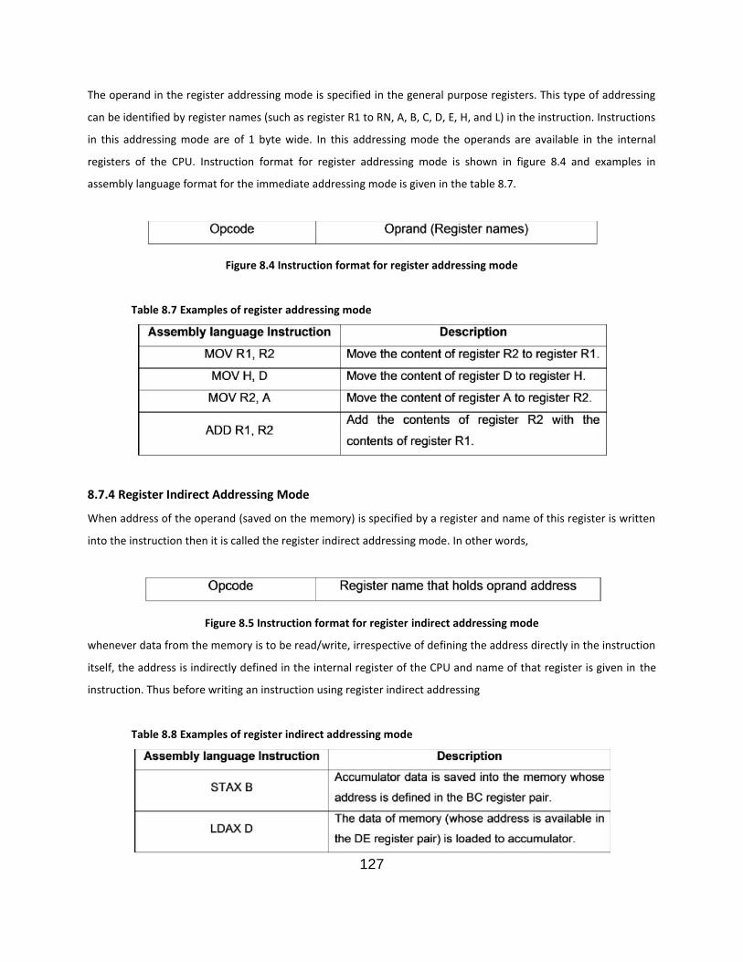
127
The operand in the register addressing mode is specified in the general purpose registers. This type of addressing
can be identified by register names (such as register R1 to RN, A, B, C, D, E, H, and L) in the instruction. Instructions
in this addressing mode are of 1 byte wide. In this addressing mode the operands are available in the internal
registers of the CPU. Instruction format for register addressing mode is shown in figure 8.4 and examples in
assembly language format for the immediate addressing mode is given in the table 8.7.
Figure 8.4 Instruction format for register addressing mode
Table 8.7 Examples of register addressing mode
8.7.4 Register Indirect Addressing Mode
When address of the operand (saved on the memory) is specified by a register and name of this register is written
into the instruction then it is called the register indirect addressing mode. In other words,
Figure 8.5 Instruction format for register indirect addressing mode
whenever data from the memory is to be read/write, irrespective of defining the address directly in the instruction
itself, the address is indirectly defined in the internal register of the CPU and name of that register is given in the
instruction. Thus before writing an instruction using register indirect addressing
Table 8.8 Examples of register indirect addressing mode
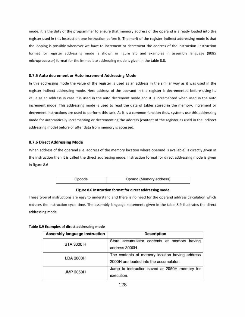
128
mode, it is the duty of the programmer to ensure that memory address of the operand is already loaded into the
register used in this instruction one instruction before it. The merit of the register indirect addressing mode is that
the looping is possible whenever we have to increment or decrement the address of the instruction. Instruction
format for register addressing mode is shown in figure 8.5 and examples in assembly language (8085
microprocessor) format for the immediate addressing mode is given in the table 8.8.
8.7.5 Auto decrement or Auto increment Addressing Mode
In this addressing mode the value of the register is used as an address in the similar way as it was used in the
register indirect addressing mode. Here address of the operand in the register is decremented before using its
value as an address in case it is used in the auto decrement mode and it is incremented when used in the auto
increment mode. This addressing mode is used to read the data of tables stored in the memory. Increment or
decrement instructions are used to perform this task. As it is a common function thus, systems use this addressing
mode for automatically incrementing or decrementing the address (content of the register as used in the indirect
addressing mode) before or after data from memory is accessed.
8.7.6 Direct Addressing Mode
When address of the operand (i.e. address of the memory location where operand is available) is directly given in
the instruction then it is called the direct addressing mode. Instruction format for direct addressing mode is given
in figure 8.6
Figure 8.6 Instruction format for direct addressing mode
These type of instructions are easy to understand and there is no need for the operand address calculation which
reduces the instruction cycle time. The assembly language statements given in the table 8.9 illustrates the direct
addressing mode.
Table 8.9 Examples of direct addressing mode

129
8.7.7 Indirect Addressing Mode
In this addressing mode the address of the operand is indirectly specified in the memory i.e. the address given in
the instruction points to the memory where address of the operand is saved. In some addressing modes, the
address field of the instruction is added to the content of a specific register in the CPU. Instruction format for
indirect addressing mode is given in figure 8.7
Figure 8.7 Instruction format for direct addressing mode
The internal register used in this method is the program counter (PC), it can be an index or a base register. Based
on the register used (one of the above registers) different addressing modes are used for different programs.
Advantage of this addressing mode is the easiness in changing the address while program is running. Example of
Indirect addressing mode:
8.7.8 Relative Addressing Mode
In the relative addressing mode, the operand address is defined as the relative position of the current instruction
address (contents of PC). In this mode, contents of the PC (program counter) are added with the address specified
in the instruction (relative address) to get the actual address of the operand. The relative address given in the
instruction is specified in the form of a positive or negative signed numbers. When this relative address is added
with the contents of the program counter, then this sum gives an effective address which is relative to the address
of the next instruction to be executed. Hence the operand is situated at short distance from the program counter
contents. Following example clarifies the concept of relative addressing mode:
As an example suppose that PC (program counter) stores the address value (hexadecimal) 3000 H and the relative
address (address part) given in the instruction is the hexadecimal number 50 H. After the instruction in hex code
form available at memory location 3000 H is fetched from the memory then program counter is incremented by
one to the hex value 3001 H.
Figure 8.8 Instruction format for relative addressing mode
130
The effective address for the instruction “JMP 50 H” is calculated by using relative address (50 H) and contents of
PC (3001 H) as under:
Effective address (where program to jump) = PC + Relative address = 3001 + 50 = 3051.
From here it is clear that the address of next instruction to be executed is 50 memory locations ahead of the
address of the next instruction. Instructions of this addressing mode are mostly used in case of the conditional or
unconditional instructions (such as JUMP, LOOP or CALL). The advantage of this addressing mode is the small
number of address bits in the instruction format due to the use of the less number of the relative address bits as
compared to the complete address of memory. Instruction format for relative addressing mode is given in figure
8.8.
Here Operand address = Relative address (Offset) + PC.
8.7.9 Indexed Addressing Mode
In this addressing mode the data in the index register is added with the operand (address given in the instruction)
address to get the actual address of the operand. In most of cases, the index register is an special register available
internally in the CPU. The value available in this register is used as the index value to be used for the address
calculation of the operand. The address written into the instruction (operand) i.e. address field, is used as the
starting address of the series of numbers stored at the memory. Whenever a series of numbers is to be accessed,
address of the first number is written into the instruction and then to read these contents (1st number of the
series), index register is loaded with the value zero so that sum of the index register and the address in the
instruction be equal to the address of the 1st number of the series be accessed.
Thus whatever next number is to be read from this series the value in the index register is loaded in accordance
that how far this number is from the first number of the series. The index registers can be incremented or
decremented if the numbers of the series are to be read in the continuity in the upwards or the downward
direction. In the computer systems with many inbuilt CPU registers, any one of these can be used as the index
register. Operand address can be calculated as per the following relation:
Operand address = Address (available in instruction) + Contents of index register
8.7.10 Base Register Addressing Mode
This mode is used for re-allocation of the programs available in the memory (from one area to another). In the
base register addressing mode address is given in the instruction which is further added with the contents of the
base register to get the actual address of the operand lying at the memory. The concept of indexed addressing
mode and the base register addressing mode is somewhat comparable. These modes are differentiated as per the
use of the registers and the way they are represented in the instruction, not the way these are used for the
address computations. In case of indexed addressing, relative address to be added to get the operand address is
131
loaded in the index register. On other hand in the base register addressing mode, relative address is available in
the instruction. Instruction format for relative addressing mode is given in figure 8.9.
Here Operand address = <Base register> +Offset.
Figure 8.9 Instruction format for base register addressing mode
During data transfer in between the memory i.e. from one group of locations to another, the address specified in
the instruction (using this addressing mode) reflects the position of the data from its starting position. By using
base register addressing mode, the displacement value of the instructions need not to change. Only the base
register value is required to be updated, for selecting the new memory location.
8.8 Self Assessment Questions (Section 8.7)
1. “LDAX D” Instruction belongs to____________ addressing mode.
A. Register indirect
B. Implied
C. Direct
D. Register
2. Stack-organized instruction belongs to___________ addressing
A. Two-addressing
B. Indirect addressing
C. Indexed addressing
D. Zero addressing
3. k-bit field can represent________.
A. 3k registers
B. 2k registers
C. K2 registers
D. K3 registers
4. Addressing mode(s) that uses program counter instead of a general purpose register is ______.
A. Indexed
B. Relative
C. Direct
D. A and C both
5. The addressing mode, where operand value is directly specified in the syntax (instruction) is
called_____.
A. Definite addressing mode
B. Direct addressing mode

132
C. Immediate addressing mode
D. Relative addressing mode
6. Name the addressing mode where PC (program counter) is added with the address given in the
instruction to get the address of the operand.
A. Indexed addressing mode
B. Implied Mode
C. Register Addressing Mode
D. Relative Addressing mode
7. Addressing mode techniques are used by the CPU for _____________________.
A. Facilitating the programmers by having facilities to use memory pointers, up/down
counters etc.
B. Reducing the number of bits in the operand part of instruction
C. Specifying rules for interpreting or modifying address field of the instruction
D. All of the above
8. The addressing mode used in an instruction “STA 2000 H”, is
A. Immediate
B. Indirect
C. Direct
D. Index
9. Which of the following instruction belongs to the register addressing mode?
A. MOV R1, #65H
B. MOV R1, R2
C. MVI A, 87H
D. None of these
10. Operand address = <Base register> +Offset belongs to_________addressing mode
A. Zero addressing
B. Index register
C. Indirect
D. Base register
8.9 Summary
Addressing modes defines the way by which the operands are placed in the instruction.
Every instruction has two parts such as Opcode (operation code) and Operand.
Opcode is the part of instruction that tells us about the operation to be performed.
Operand is the part of the instruction on which the operation is performed
Address of the instruction to be executed is held in the PC (program counter).
133
Fetch, decode and execution are the three steps that the CPU follows to perform a task based on
the instruction.
Based on the address defined in the operand, instructions can be classified as three/two/one/zero
address instructions.
The effective address of the instruction is obtained after performing some calculations.
The most common addressing modes used in majority of the processors are: Register Mode,
Implied Mode, Register Indirect Mode, Auto-increment or Auto-decrement Mode, Direct Mode,
Indirect Mode, Relative address Mode, Immediate Mode, Index register Mode and Base Register
Mode.
Addressing modes can be summarized as:
134
8.10 Glossary
Opcode – Defines the operation to be performed.
Operand – Data on which the operation is performed.
Mode field – Position of the operand.
Address field- Designate a memory address or a processor register
Register – 8/16 bit storage device designed using 8/16 flip flops.
Register Transfer – Transfer of data from one register to another.
PC – Program Counter
CPU – Central processing Unit
Memory – Group of Flip flops to store binary data
RISC – Reduced Instruction Set Computer
CISC – Complex Instruction Set Computer
TOS – Top of stack
LIFO – Last in First Out
Instruction cycle – Time taken by the CPU to complete execution of one instruction
Memory Read – Transfer of data from memory to other devices (registers).
Memory Write – Transfer of data from other devices (registers) to memory.
8.11 Answers to check your progress/Suggested Answers to QuestionsSection (8.1 to 8.3)
13. Opcode, Operand
14. Opcode fetch
15. B
16. A
17. Program counter
Section (8.5)
20. Implied Addressing Mode
21. D
22. A
23. B
24. B
25. C
Section (8.7)
1. A

135
2. D
3. B
4. A
5. C
6. A
7. D
8. C
9. B
10. D
8.12 Bibliography/References/Suggested Readings
20. M. Morris Mano, Computer System Architecture, Pearson Publication.
21. J.P. Hays, Computer Architecture and Organization, Tata McGraw-Hill Publishing.
22. B Govindarajalu, Computer Architecture and Organization (Design Principles and Applications), McGraw
Hill.
23. J. L. Hennessy and D. A. Patterson, Computer Architecture: A Quantitative Approach, San Francisco, CA,
fifth edition
24. William Stallings, Computer Organization and Architecture, Pearson Publication
25. Pal Choudhary, Computer Organization and Design, PHI
26. www.nptel.iitm.ac.in
8.13 Terminal and Model Questions
1. What is an instruction format?
2. Differentiate direct and indirect addressing modes.
3. Write addressing modes of the following instructions:
a. LDA 2030H
b. ADD R1, R2
c. LOAD R1, X
d. JUMP Address
e. MOVE (B), R1
f. ADD R1, #65H
4. Explain and differentiate one address and two address Instructions.
5. What is an Effective address?
6. Define program Counter.
7. How effective address is calculated from the relative address?
8. Why instructions are classified into different addressing modes? Explain the concept of the addressing mode
136
Lesson 9
Input/output (I/O) Organization
Structure
9.1 Objectives
9.2 Introduction
9.3 Accessing Peripheral (I/O) Devices
9.3.1 Input/output Bus and Interface Modules
9.3.2 The I/O Processor
9.4 I/O Mapping
9.4.1 Memory-Mapped I/O
9.4.2 Isolated I/O Mapping
9.4.3 Comparison between Memory-Mapped and Isolated I/O
9.5 I/O Interface Hardware Required-The I/O Port
9.6 USB Port
9.6.1 Features of USB
9.6.2 Versions of USB
9.7 Serial Port
9.8 Parallel Port
9.9 Network Port
9.10 Summary
9.11 Glossary
9.12 Suggestive answers to Self Assessment Questions (SAQ)
9.13 Bibliography/References/Suggested Readings
9.14 Terminal and Model Questions
9.1 Objectives
The students will gain knowledge about the following after studying this chapter
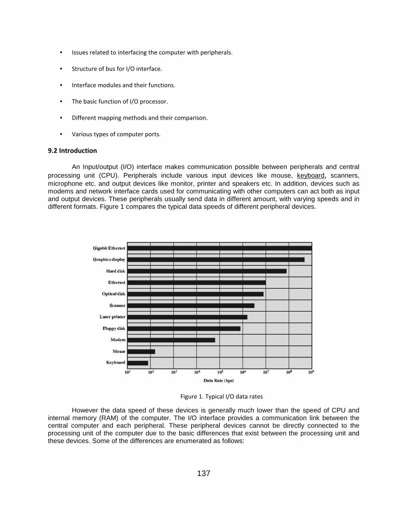
137
Issues related to interfacing the computer with peripherals.
Structure of bus for I/O interface.
Interface modules and their functions.
The basic function of I/O processor.
Different mapping methods and their comparison.
Various types of computer ports.
9.2 Introduction
An Input/output (I/O) interface makes communication possible between peripherals and centralprocessing unit (CPU). Peripherals include various input devices like mouse, keyboard, scanners,microphone etc. and output devices like monitor, printer and speakers etc. In addition, devices such asmodems and network interface cards used for communicating with other computers can act both as inputand output devices. These peripherals usually send data in different amount, with varying speeds and indifferent formats. Figure 1 compares the typical data speeds of different peripheral devices.
However the data speed of these devices is generally much lower than the speed of CPU andinternal memory (RAM) of the computer. The I/O interface provides a communication link between thecentral computer and each peripheral. These peripheral devices cannot be directly connected to theprocessing unit of the computer due to the basic differences that exist between the processing unit andthese devices. Some of the differences are enumerated as follows:
Figure 1. Typical I/O data rates
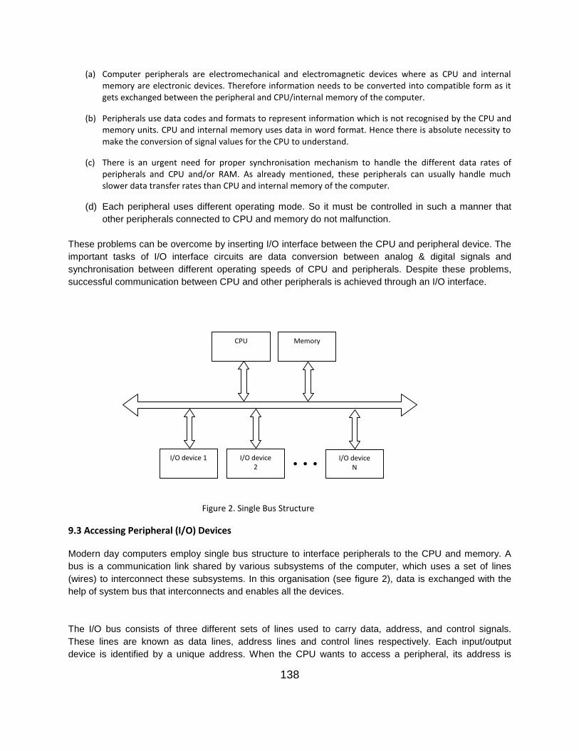
138
(a) Computer peripherals are electromechanical and electromagnetic devices where as CPU and internalmemory are electronic devices. Therefore information needs to be converted into compatible form as itgets exchanged between the peripheral and CPU/internal memory of the computer.
(b) Peripherals use data codes and formats to represent information which is not recognised by the CPU andmemory units. CPU and internal memory uses data in word format. Hence there is absolute necessity tomake the conversion of signal values for the CPU to understand.
(c) There is an urgent need for proper synchronisation mechanism to handle the different data rates ofperipherals and CPU and/or RAM. As already mentioned, these peripherals can usually handle muchslower data transfer rates than CPU and internal memory of the computer.
(d) Each peripheral uses different operating mode. So it must be controlled in such a manner thatother peripherals connected to CPU and memory do not malfunction.
These problems can be overcome by inserting I/O interface between the CPU and peripheral device. Theimportant tasks of I/O interface circuits are data conversion between analog & digital signals andsynchronisation between different operating speeds of CPU and peripherals. Despite these problems,successful communication between CPU and other peripherals is achieved through an I/O interface.
9.3 Accessing Peripheral (I/O) Devices
Modern day computers employ single bus structure to interface peripherals to the CPU and memory. Abus is a communication link shared by various subsystems of the computer, which uses a set of lines(wires) to interconnect these subsystems. In this organisation (see figure 2), data is exchanged with thehelp of system bus that interconnects and enables all the devices.
The I/O bus consists of three different sets of lines used to carry data, address, and control signals.These lines are known as data lines, address lines and control lines respectively. Each input/outputdevice is identified by a unique address. When the CPU wants to access a peripheral, its address is
• • •
CPU Memory
I/O device 1 I/O device2
I/O deviceN
Figure 2. Single Bus Structure

139
placed on the address lines. All the peripheral interfaces continuously monitor address lines. When aperipheral identifies its address, it responds through control lines. All the other peripherals, whoseaddresses do not match with the contents of the address bus, are disabled by their interfaces. The CPUmay request either a read or a write operation. Then data lines are used to transfer data. Versatility andlow cost are the two major advantages of the bus organization.
9.3.1 I/O Bus and Interface Modules
A generalised set up of interconnection between CPU and a variety of peripherals is illustrated in figure 3. The I/Obus comprises of data lines, address lines and control lines. The bus provides connecting medium to enableinformation exchange between all the devices connected to CPU and memory. The peripheral devices such asprinter, mouse, keyboard, magnetic disc, tapes etc. are associated with their respective interface modules. Eachinterface unit can decode the address sent by the CPU, synchronise the data flow between the peripheral and CPUand control this flow. The functions of each of data, address and control lines are described as follows:
Data lines: These lines are used to transfer data between CPU and peripheral devices. Data is sent either serially,one bit at a time or in parallel as multiples of 8-bits at a time. Parallel data transfer is much faster, but it requiresmore hardware.
Address lines: These lines are used by the CPU to select a particular peripheral device. Each peripheral device isidentified by a unique address. The interface module attached to a peripheral device contains an address decoderwhich continuously checks the address lines. On detecting its own address, it enables the interconnecting pathbetween the address bus and the peripheral device under its control. All other peripherals are then disables bytheir interface modules.
Control lines: These lines provide synchronisation and timings information required for the flow of data andinformation between the CPU and its peripheral devices. It is important to note that the CPU views I/O operationssimilar to memory operations and each device has a unique identifier or address. The CPU issues commands thatcontain device address. Peripheral communications with CPU are controlled by I/O modules, whose function is tointerface the peripheral with CPU or memory through bus.

140
9.3.2 The I/O Processor
The CPU needs to communicate with memory as well as I/O devices. Similar to I/O bus, the memory bus alsocontains data, address and control lines to carry out the required operations between CPU and memory. In fact,computer buses can be used in three different ways to make communication with memory and I/O as follows:
(a) Use separate set of buses for each of memory and I/O.
(b) Use common bus for both memory and I/O, but separate control lines.
(c) Use common bus and a common set of control lines for memory as well as I/O.In computers, where separate set of data, address and control lines are used for memory and I/O operations, as infirst method, an I/O processor (IOP) is incorporated to assist the CPU. The task of IOP is to provide separatemedium for information transfer between the peripheral devices and the system memory. The IOP is also knownas a data channel. A typical computer system can have one CPU and at least one IOP. The figure 4 depicts the blockdiagram of a computer containing one IOP. An IOP is similar to a CPU, except that it is designed to do I/Ooperations only. An IOP can fetch and execute its own instructions without any control of the CPU. It can performarithmetic, logic, branching and code translation operations also.The CPU performs its usual task of processing data according to instructions. The task of IOP is to provide a pathfor transfer of data between the system memory and peripheral devices. Normally CPU acts as the masterprocessor and IOP as the slave. However, once the CPU initiates the I/O program, the IOP starts operating
Address bus
PrinterMouse Keyboard
CPU
InterfaceModule 3
InterfaceModule 1
InterfaceModule 2
I/O bus
Data bus
Control bus
Figure 3. Connections of CPU with Peripheral Devices.
Memory Unit
IOP
CPU
Peripheral Devices
I/O bus
Figure 4. Block diagram of a computer system with an IOP

141
independently. Instructions read by the IOP from system memory are called commands. They have similar functionas instructions.
Self Assessment Test 1
Q1. What major problems are encountered while interfacing CPU with peripherals?
Q2. Explain bus structure. How I/O devices are accessed?
Q3. Describe the functions of data, address and control lines.
Q4. What is an I/O processor? Describe its function.
9.4 I/O Mapping
In many computer systems, the CPU, system memory and the I/O devices share a common bus. This bus is used toshare the data and control signals between the CPU and memory or I/O devices. In such systems, a memorytransfer operation is distinguished from an I/O transfer operation by employing separate read and write controllines. The CPU enables the I/O read and I/O write lines during an I/O transfer, whereas it enables memory read andmemory write control lines when it wants to access a memory location. In such systems, two methods are used toperform I/O operations between the CPU and peripherals:
(a) Memory-mapped I/O
(b) Isolated I/O
9.4.1 Memory-Mapped I/O
In this method, a common address space is used for both memory locations and I/O devices. Here one commonset of read and write control signals is used by the computer and no distinction is made between the memory andI/O addresses. The processor addresses peripheral devices same as a memory location. In this scheme, there areno separate I/O instructions. If address bus has 10 lines, for example, 210 = 1024 I/O addresses and memorylocations can be addressed in totality. Some of the addresses may be assigned to memory locations and theremaining to peripherals. In some systems, a portion of total address space is reserved for I/O interface modules,but generally any address can be used to locate them. Most of the computer systems use memory-mapped I/Omethod.
9.4.2 Isolated I/O Mapping
In this method of mapping, separate address spaces are dedicated to memory locations and I/O devices. NormallyI/O devices use a much smaller chunk of memory space. The system bus contains memory read/write and IN/OUTcontrol lines. Here the status of control line specifies whether the address refers to a memory location or an I/Odevice. For example, Intel 8085 microprocessor issues a high signal to identify an I/O device and a low signal for amemory location. IN and OUT instructions are executed to read data from an input device and to send data to anoutput device respectively.
9.4.3 Comparison between Memory-Mapped and Isolated I/O:
Memory-mapped I/O Isolated I/O
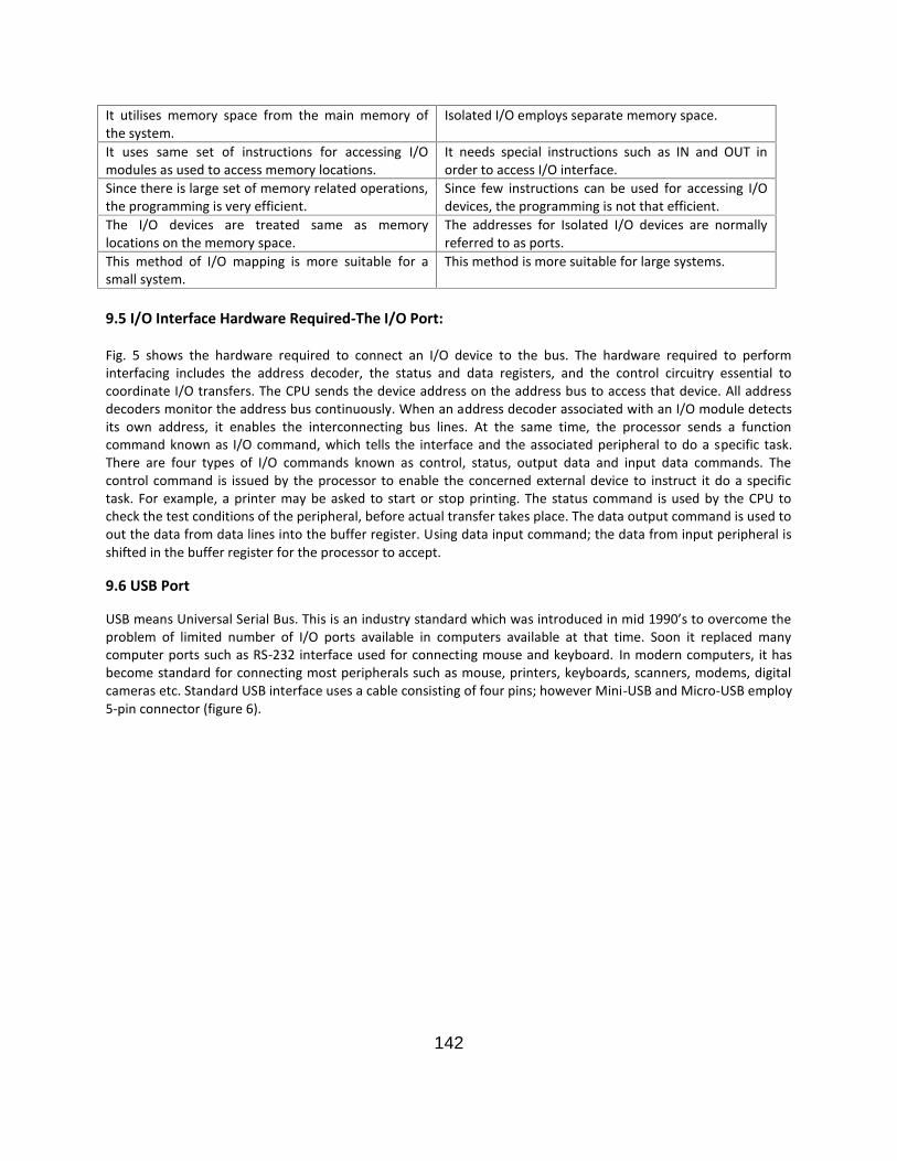
142
It utilises memory space from the main memory ofthe system.
Isolated I/O employs separate memory space.
It uses same set of instructions for accessing I/Omodules as used to access memory locations.
It needs special instructions such as IN and OUT inorder to access I/O interface.
Since there is large set of memory related operations,the programming is very efficient.
Since few instructions can be used for accessing I/Odevices, the programming is not that efficient.
The I/O devices are treated same as memorylocations on the memory space.
The addresses for Isolated I/O devices are normallyreferred to as ports.
This method of I/O mapping is more suitable for asmall system.
This method is more suitable for large systems.
9.5 I/O Interface Hardware Required-The I/O Port:
Fig. 5 shows the hardware required to connect an I/O device to the bus. The hardware required to performinterfacing includes the address decoder, the status and data registers, and the control circuitry essential tocoordinate I/O transfers. The CPU sends the device address on the address bus to access that device. All addressdecoders monitor the address bus continuously. When an address decoder associated with an I/O module detectsits own address, it enables the interconnecting bus lines. At the same time, the processor sends a functioncommand known as I/O command, which tells the interface and the associated peripheral to do a specific task.There are four types of I/O commands known as control, status, output data and input data commands. Thecontrol command is issued by the processor to enable the concerned external device to instruct it do a specifictask. For example, a printer may be asked to start or stop printing. The status command is used by the CPU tocheck the test conditions of the peripheral, before actual transfer takes place. The data output command is used toout the data from data lines into the buffer register. Using data input command; the data from input peripheral isshifted in the buffer register for the processor to accept.
9.6 USB Port
USB means Universal Serial Bus. This is an industry standard which was introduced in mid 1990’s to overcome theproblem of limited number of I/O ports available in computers available at that time. Soon it replaced manycomputer ports such as RS-232 interface used for connecting mouse and keyboard. In modern computers, it hasbecome standard for connecting most peripherals such as mouse, printers, keyboards, scanners, modems, digitalcameras etc. Standard USB interface uses a cable consisting of four pins; however Mini-USB and Micro-USB employ5-pin connector (figure 6).
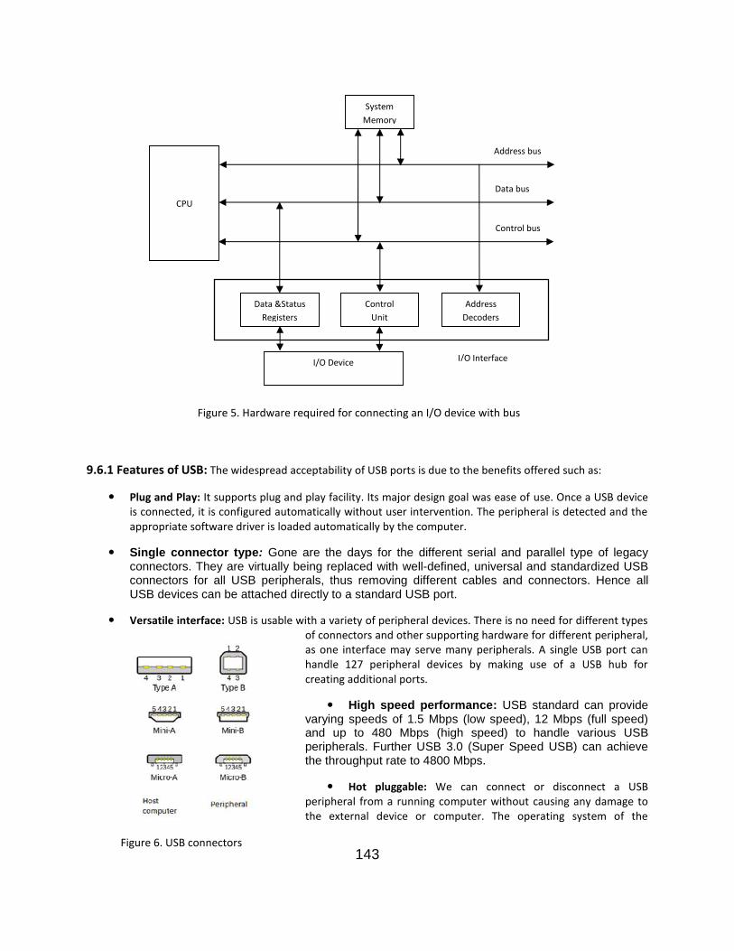
143
9.6.1 Features of USB: The widespread acceptability of USB ports is due to the benefits offered such as:
Plug and Play: It supports plug and play facility. Its major design goal was ease of use. Once a USB deviceis connected, it is configured automatically without user intervention. The peripheral is detected and theappropriate software driver is loaded automatically by the computer.
Single connector type: Gone are the days for the different serial and parallel type of legacyconnectors. They are virtually being replaced with well-defined, universal and standardized USBconnectors for all USB peripherals, thus removing different cables and connectors. Hence allUSB devices can be attached directly to a standard USB port.
Versatile interface: USB is usable with a variety of peripheral devices. There is no need for different typesof connectors and other supporting hardware for different peripheral,as one interface may serve many peripherals. A single USB port canhandle 127 peripheral devices by making use of a USB hub forcreating additional ports.
High speed performance: USB standard can providevarying speeds of 1.5 Mbps (low speed), 12 Mbps (full speed)and up to 480 Mbps (high speed) to handle various USBperipherals. Further USB 3.0 (Super Speed USB) can achievethe throughput rate to 4800 Mbps.
Hot pluggable: We can connect or disconnect a USBperipheral from a running computer without causing any damage tothe external device or computer. The operating system of the
Figure 5. Hardware required for connecting an I/O device with bus
Address bus
CPUData bus
Control bus
Data &StatusRegisters
ControlUnit
AddressDecoders
I/O InterfaceI/O Device
SystemMemory
Figure 6. USB connectors
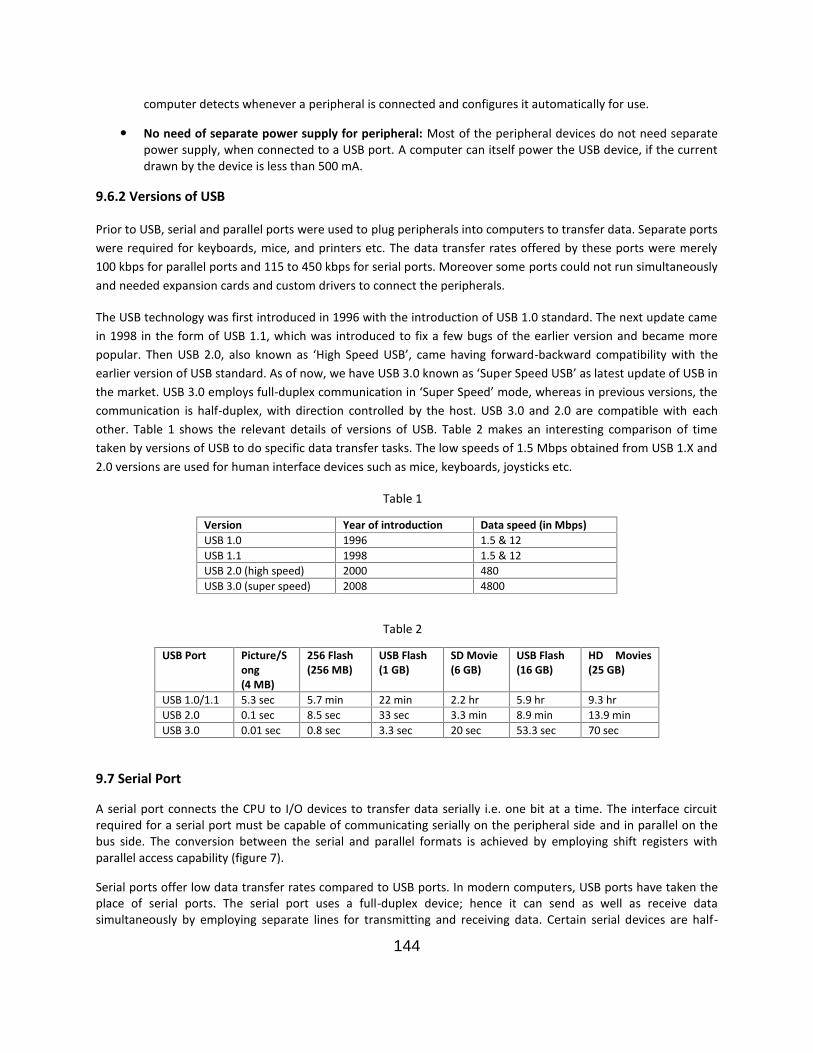
144
computer detects whenever a peripheral is connected and configures it automatically for use.
No need of separate power supply for peripheral: Most of the peripheral devices do not need separatepower supply, when connected to a USB port. A computer can itself power the USB device, if the currentdrawn by the device is less than 500 mA.
9.6.2 Versions of USB
Prior to USB, serial and parallel ports were used to plug peripherals into computers to transfer data. Separate portswere required for keyboards, mice, and printers etc. The data transfer rates offered by these ports were merely100 kbps for parallel ports and 115 to 450 kbps for serial ports. Moreover some ports could not run simultaneouslyand needed expansion cards and custom drivers to connect the peripherals.
The USB technology was first introduced in 1996 with the introduction of USB 1.0 standard. The next update camein 1998 in the form of USB 1.1, which was introduced to fix a few bugs of the earlier version and became morepopular. Then USB 2.0, also known as ‘High Speed USB’, came having forward-backward compatibility with theearlier version of USB standard. As of now, we have USB 3.0 known as ‘Super Speed USB’ as latest update of USB inthe market. USB 3.0 employs full-duplex communication in ‘Super Speed’ mode, whereas in previous versions, thecommunication is half-duplex, with direction controlled by the host. USB 3.0 and 2.0 are compatible with eachother. Table 1 shows the relevant details of versions of USB. Table 2 makes an interesting comparison of timetaken by versions of USB to do specific data transfer tasks. The low speeds of 1.5 Mbps obtained from USB 1.X and2.0 versions are used for human interface devices such as mice, keyboards, joysticks etc.
Table 1
Version Year of introduction Data speed (in Mbps)USB 1.0 1996 1.5 & 12USB 1.1 1998 1.5 & 12USB 2.0 (high speed) 2000 480USB 3.0 (super speed) 2008 4800
Table 2
USB Port Picture/Song(4 MB)
256 Flash(256 MB)
USB Flash(1 GB)
SD Movie(6 GB)
USB Flash(16 GB)
HD Movies(25 GB)
USB 1.0/1.1 5.3 sec 5.7 min 22 min 2.2 hr 5.9 hr 9.3 hrUSB 2.0 0.1 sec 8.5 sec 33 sec 3.3 min 8.9 min 13.9 minUSB 3.0 0.01 sec 0.8 sec 3.3 sec 20 sec 53.3 sec 70 sec
9.7 Serial Port
A serial port connects the CPU to I/O devices to transfer data serially i.e. one bit at a time. The interface circuitrequired for a serial port must be capable of communicating serially on the peripheral side and in parallel on thebus side. The conversion between the serial and parallel formats is achieved by employing shift registers withparallel access capability (figure 7).
Serial ports offer low data transfer rates compared to USB ports. In modern computers, USB ports have taken theplace of serial ports. The serial port uses a full-duplex device; hence it can send as well as receive datasimultaneously by employing separate lines for transmitting and receiving data. Certain serial devices are half-
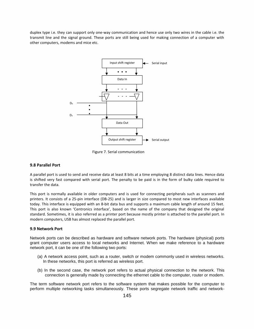
145
duplex type i.e. they can support only one-way communication and hence use only two wires in the cable i.e. thetransmit line and the signal ground. These ports are still being used for making connection of a computer withother computers, modems and mice etc.
9.8 Parallel Port
A parallel port is used to send and receive data at least 8 bits at a time employing 8 distinct data lines. Hence datais shifted very fast compared with serial port. The penalty to be paid is in the form of bulky cable required totransfer the data.
This port is normally available in older computers and is used for connecting peripherals such as scanners andprinters. It consists of a 25-pin interface (DB-25) and is larger in size compared to most new interfaces availabletoday. This interface is equipped with an 8-bit data bus and supports a maximum cable length of around 15 feet.This port is also known ‘Centronics interface’, based on the name of the company that designed the originalstandard. Sometimes, it is also referred as a printer port because mostly printer is attached to the parallel port. Inmodern computers, USB has almost replaced the parallel port.
9.9 Network Port
Network ports can be described as hardware and software network ports. The hardware (physical) portsgrant computer users access to local networks and Internet. When we make reference to a hardwarenetwork port, it can be one of the following two ports:
(a) A network access point, such as a router, switch or modem commonly used in wireless networks.In these networks, this port is referred as wireless port.
(b) In the second case, the network port refers to actual physical connection to the network. Thisconnection is generally made by connecting the ethernet cable to the computer, router or modem.
The term software network port refers to the software system that makes possible for the computer toperform multiple networking tasks simultaneously. These ports segregate network traffic and network-
• • •
•
Input shift register
Data In
Serial input
Data Out
Output shift register Serial output
•••
•
D0
D7
• • •
•
• • •
•
Figure 7. Serial communication
146
based services into separate segments. The computer can then prioritize and process these segments, inthe same manner as it does with its internal operations.
A network port is identified as a 16-bit unsigned integer. Hence there can be a total of 216 = 65536network ports numbering from 0 to 65535. Each active network port can support bidirectional flow ofinformation. Most of the ports numbered from 0 to 1023 are needed for specific Internet tasks. Thesetasks include computer processes such as e-mail, web browsing and telnet. Other computer programssuch as downloading, and video games have user-defined ports. Internal operations are under constantmonitoring by the computer whereas user-defined operations are monitored only when they are running.
Self Assessment 2
Q1. Peripherals are ___________ devices.
(a) Electronic(b) Electromechanical/Electromagnetic(c) Mechanical(d) Logical
Q2. In memory mapped I/O addressing, the address space is shared by
(a) I/O devices and memory(b) CPU and address bus(c) Buses and hardware(d) I/O interface
Q3. The instructions used to address a peripheral device in Isolated mapped I/O method, are
(a) Move instructions(b) Read and write instructions(c) IN and OUT instructions(d) None of the above
Q4. The main function of I/O bus is to exchange information between ___________ and I/Odevices through their I/O interface.
(a) Memory(b) Control bus(c) Address bus(d) CPU
Q5. The main function of ________ bus is to transfer information between processor and main memory.
(a) Data(b) Address(c) Memory(d) Control
Q6. The method which employs separate set of read and write control lines is
(a) Memory-mapped I/O(b) Isolated I/O method(c) None of the above
147
Q7. Parallel port uses an interface consisting of
(a) 20 pins(b) 30 pins(c) 24 pins(d) None of the above
Q8. Which computer port is most commonly used these days?
(a) Serial port(b) Parallel port(c) USB port(d) All of above
Q9. The total numbers of network ports in a computer system can be__________
Q10. What are the advantages offered by USB port?
Q11. Describe various generations of USB. Compare the available data speeds.
9.10 Summary
The CPU needs to access the peripheral (I/O) devices for interacting with the outside world. These devices cannotbe directly connected to the computer. They can be connected to the computer through an I/O interface only. Thisinterface contains not only the physical connectors to do its function, but also the necessary logic for executingcommunication between the peripheral and the bus. The peripheral device is connected to the CPU through set oflines known as I/O bus. This bus consists of data, address and control lines. In addition to communication with I/Odevices, the processor needs to exchange information with the memory units also. It may use a separate memorybus for this purpose, or alternately single bus structure may also be used. In single bus structure, common bus isused by both I/O devices and memory units to interact with the CPU. In this set up, the CPU can address the I/Odevices in two distinct ways namely memory-mapped I/O and isolated I/O.
There are many ports in a computer through which data and information can be exchanged with the computerfrom outside. These are serial port, parallel port, USB port and network port. Serial port allows one bit ofinformation at a time, whereas parallel port allows at least 8-bits of data at a time. However USB port is mostcommonly used as it offers many advantages over the other two. Network port can be a physical port or asoftware defined port. A computer can have 65536 network ports.
9.11 Glossary
Address Bus: CPU uses this bus to select a particular peripheral device. Each peripheral device is identifiedby a unique address by the CPU.
Bus: A bus is a shared communication link that uses set of wires to interconnect different subsystems ofthe computer.
Control Bus: It provides the necessary synchronisation and timings signals required for the flow of data orinformation between the processor and I/O (peripheral) devices.
Data Bus: It is a shared communication link used to transfer the data between the processor and I/Odevices.

148
I/O Bus: It controls and synchronises the data flow between the CPU and peripherals.
I/O Commands: I/O commands are required for a particular interface when it is addressed by the CPU.
I/O Mapping: These methods are used to perform I/O tasks between the CPU and other peripheraldevices.
Isolated I/O: Method of I/O mapping, in which two separate address spaces are used for memorylocations and I/O devices.
Memory Bus: This bus is used to exchange information between the processor and the main memory.
Memory-Mapped I/O: In this technique, the CPU addresses an I/O device same as a memory location.
Peripheral Devices: These are electromechanical/electromagnetic devices which communicate with theprocessor from outside world. Examples are keyboard, mouse, printer, sensors, modems, magnetic disc ortapes etc.
USB: Universal serial bus, an industry standard used to standardise the connection of peripherals tocomputer for both data transfer and electric power supply.
9.12 Suggestive answers to Self Assessment Questions (SAQ)
Self Assessment Test 1
Ans. 1 See section 9.2.
Ans. 2 Most of the modern day computers employ single bus arrangement to connect I/O devices to CPU andsystem memory. The I/O bus consists of three separate sets of lines used to transfer data, address, andcontrol signals.
Ans. 3 Data lines: Data means information. Data lines are used to exchange data between CPU and I/O devices.
Address lines: Every peripheral device is identified by a unique address. Address lines are used by the CPUto place the address of the peripheral with which it wants to communicate.
Control lines: These are used to provide synchronization and timing signals required for the flow of dataand information between the CPU and peripheral devices.
Ans. 4 In computers, where separate set of data, address and control lines are used each for memory and I/Ooperations, a separate I/O processor (IOP) is incorporated in addition to CPU. The task of IOP is to provideseparate medium for information transfer between the peripheral devices and the system memory.
Self Assessment Test 2
Ans. 1 (b) Electromechanical/Electromagnetic
Ans. 2 (a) I/O devices and memory
Ans. 3 (c) IN and OUT instructions
Ans. 4 (d) CPU
Ans. 5 (c) Memory
Ans. 6 (b) Isolated I/O method
149
Ans. 7 (c) 24 pins
Ans. 8 (c) USB port
Ans. 9 65536
Ans. 10 See section 9.6.1
Ans. 11 See section 9.6.2
9.13 Bibliography/References/Suggested Readings
(1) Computer System Architecture, M. Morris Manno, 3rd Edition, Pearson Education.(2) Computer Organization and Architecture, William Stallings, 8th Edition, Pearson Education.(3) Structured Computer Organization, Andrew S. Tanenbaum, Prentice Hall of India.
9.14 Terminal and Model Questions
Q1. What are peripheral devices? Can these devices be directly connected to the computer? Explain.
Q2. How is single bus structure used for accessing I/O devices?
Q3. Describe the function an I/O processor. How is it different from main processor of the computer?
Q4. Explain memory-mapped I/O method. What are its merits and demerits?
Q5. Describe Isolated I/O method. Compare this method with memory-mapped I/O method. Which method willyou prefer and why?
Q6. What is an I/O interface? What are its major functions?
Q7. Explain in detail how you can describe a network port.
Q8. Differentiate between serial port and parallel port.
Q9. Define USB standard. Describe its various versions. State reasons for its widespread popularity.

150
Lesson 10
I/O Data Transfer Techniques
Structure
10.0 Objectives
10.1 Introduction10.2 Modes of Data Transfer
10.2.1 Programmed I/O10.2.2 Interrupt Initiated I/O10.2.3 Direct Memory Access (DMA) Controller
10.2.3.1 Burst Data Transfer10.2.3.2 Cycle stealing
10.3 I/O Processor (IOP)10.3.1 CPU-IOP Sequence
10.4 Summary10.5 Glossary10.6 Answer to check your progress/Suggested Answers to Questions (SAQ)10.7 References/ Bibliography/ Suggested Readings10.8 Terminal and Model Questions
10.0 Objectives
The main objectives of this chapter are:
To discuss different modes of data transfer.
To explain programmed I/O mode of data transfer.
To explain interrupt driven mode of data transfer.
To know the disadvantages of programmed I/O and interrupt driven data transfer.
To draw block diagram of DMA controller.
To explain working of DMA controller.
To know cycle stealing technique used in DMA controller and where it is used?
To know the concept of IOP.
To know the block
To know the CPU-IOP communication sequence
To know cycle stealing and burst data transfer techniques.
To know the advantages and applications of DMA.
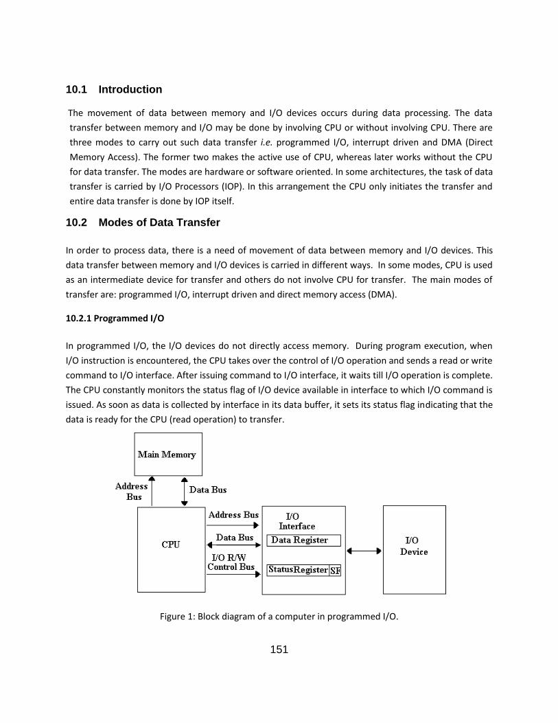
151
10.1 Introduction
The movement of data between memory and I/O devices occurs during data processing. The datatransfer between memory and I/O may be done by involving CPU or without involving CPU. There arethree modes to carry out such data transfer i.e. programmed I/O, interrupt driven and DMA (DirectMemory Access). The former two makes the active use of CPU, whereas later works without the CPUfor data transfer. The modes are hardware or software oriented. In some architectures, the task of datatransfer is carried by I/O Processors (IOP). In this arrangement the CPU only initiates the transfer andentire data transfer is done by IOP itself.
10.2 Modes of Data Transfer
In order to process data, there is a need of movement of data between memory and I/O devices. Thisdata transfer between memory and I/O devices is carried in different ways. In some modes, CPU is usedas an intermediate device for transfer and others do not involve CPU for transfer. The main modes oftransfer are: programmed I/O, interrupt driven and direct memory access (DMA).
10.2.1 Programmed I/O
In programmed I/O, the I/O devices do not directly access memory. During program execution, whenI/O instruction is encountered, the CPU takes over the control of I/O operation and sends a read or writecommand to I/O interface. After issuing command to I/O interface, it waits till I/O operation is complete.The CPU constantly monitors the status flag of I/O device available in interface to which I/O command isissued. As soon as data is collected by interface in its data buffer, it sets its status flag indicating that thedata is ready for the CPU (read operation) to transfer.
Figure 1: Block diagram of a computer in programmed I/O.

152
In case of a write operation, the CPU places data in the I/O interface buffer and proceeds to the next
instruction. A block diagram of a computer in programmed I/O mode is shown in Figure 1.
The flow diagram of programmed I/O mode for reading data from a device is given in Figure 2.
Next Instruction

153
Figure 2: Flow Diagram of Programmed I/O Data Transfer.
Disadvantage: The data transfer using this mode is slow. Since, after issuing command to I/O interface,the processor waits till I/O operation is completed. If CPU is faster than I/O, the time of CPU is wasted alot.
10.2.2 Interrupt Driven Mode
In case of interrupt driven data transfer the CPU continues to execute its own process after issuing R/Wcommands to I/O interface. After processing I/O command, the interface moves data from I/O device tointerface data register and issues an interrupt to CPU by setting an appropriate status flag in the statusregister. As the CPU has been already busy in executing its own process, after receiving interrupt, itsaves the address of process it was already executing. It then proceeds to process interrupts issued byI/O for R/W data from interface data register and store it to memory. After completing transfer, it againstarts executing its previous process. The flow diagram for reading data using interrupt driven scheme isgiven in Figure 3.
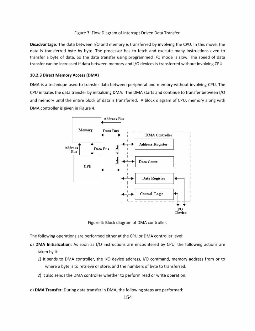
154
Figure 3: Flow Diagram of Interrupt Driven Data Transfer.
Disadvantage: The data between I/O and memory is transferred by involving the CPU. In this move, thedata is transferred byte by byte. The processor has to fetch and execute many instructions even totransfer a byte of data. So the data transfer using programmed I/O mode is slow. The speed of datatransfer can be increased if data between memory and I/O devices is transferred without involving CPU.
10.2.3 Direct Memory Access (DMA)
DMA is a technique used to transfer data between peripheral and memory without involving CPU. The
CPU initiates the data transfer by initializing DMA. The DMA starts and continue to transfer between I/O
and memory until the entire block of data is transferred. A block diagram of CPU, memory along with
DMA controller is given in Figure 4.
Figure 4: Block diagram of DMA controller.
The following operations are performed either at the CPU or DMA controller level:
a) DMA Initialization: As soon as I/O instructions are encountered by CPU, the following actions aretaken by it:1) It sends to DMA controller, the I/O device address, I/O command, memory address from or to
where a byte is to retrieve or store, and the numbers of byte to transferred.
2) It also sends the DMA controller whether to perform read or write operation.
b) DMA Transfer: During data transfer in DMA, the following steps are performed:
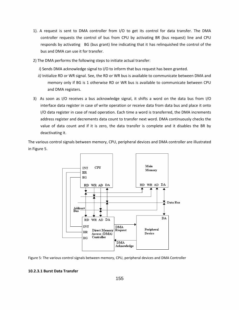
155
1). A request is sent to DMA controller from I/O to get its control for data transfer. The DMAcontroller requests the control of bus from CPU by activating BR (bus request) line and CPUresponds by activating BG (bus grant) line indicating that it has relinquished the control of thebus and DMA can use it for transfer.
2) The DMA performs the following steps to initiate actual transfer:
i) Sends DMA acknowledge signal to I/O to inform that bus request has been granted.ii) Initialize RD or WR signal. See, the RD or WR bus is available to communicate between DMA and
memory only if BG is 1 otherwise RD or WR bus is available to communicate between CPUand DMA registers.
3) As soon as I/O receives a bus acknowledge signal, it shifts a word on the data bus from I/Ointerface data register in case of write operation or receive data from data bus and place it ontoI/O data register in case of read operation. Each time a word is transferred, the DMA incrementsaddress register and decrements data count to transfer next word. DMA continuously checks thevalue of data count and if it is zero, the data transfer is complete and it disables the BR bydeactivating it.
The various control signals between memory, CPU, peripheral devices and DMA controller are illustratedin Figure 5.
Figure 5: The various control signals between memory, CPU, peripheral devices and DMA Controller
10.2.3.1 Burst Data Transfer
156
Generally, a high speed peripheral uses the DMA to data transfer and it takes the control of bus tillentire block of data is transferred. Such a transfer is called as burst.
10.2.3.2 Cycle Stealing
If the slow speed peripheral intends to use DMA for transfer, then cycle stealing technique is used so
that CPU time may be utilized properly. It allows one word to transfer at a time after which it returns the
control of bus to CPU. Here, DMA controller steals a cycle of CPU for data transfer. Cycle stealing is
slower as compared to burst.
Advantages: The various advantages of data transfer using DMA controller are:
1) Fast transfer of data between high speed storage and memory i.e. almost at the speed of high speedstorage.
2) The technique is easy to implement.
Applications: The DMA is used in various applications. The two such applications are:
1) Fast transfer of information between magnetic disk and memory.2) Updating display in interactive terminals.
Check Your Progress
Q. 1 : In polling , a _ __ __ __ _ _ monitors the interrupt status flag to check if any interrupt issued by anI/O device.
Answer options: a) hardware chip b) a process c) a processor d) I/O device.
Q. 2 : The term DMA stands for _ __ __ __ __ __ __ ___ __ __.
Answer options: a) Digital Memory Access. b) Direct Memory Access.
c) Direct Memory Arbitration. d) Daisy Memory Allocation.
Q 3: Cycle stealing technique is used in ________________________________________
Answer options: a). Priority Interrupt b) DMA c) Interrupt Driven d) Programmed I/O
Q 4: The data transfer rate using programmed I/O or interrupt driven modes is __________ if it iscompared with DMA.
Answer options: a) almost same b) fast c) slow d) Not any
Q 5: In DMA mode of data transfer, the technique, in which a high speed peripheral takes the control ofbus till entire block of data is transfer, is called as__________________
Answer options: a) polling b) cycle stealing c) burst d) Not any
Q 6: The speed of cycle stealing is __________________ as compared to burst.
Answer options: a) same b) fast c) slow d) very fast
Q 7: In DMA mode, the ________________ initializes the data transfer.
Answer options: a) DMA b) CPU c) CPU & DMA d) None
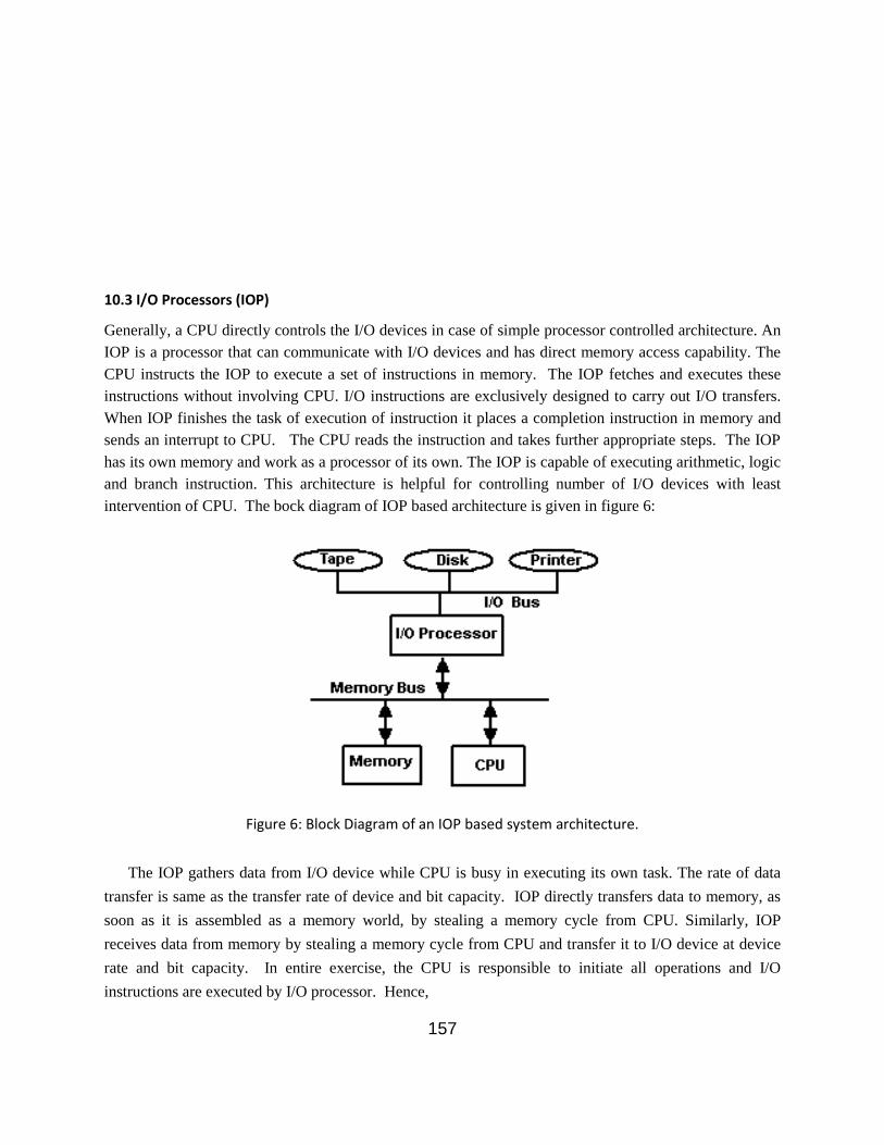
157
10.3 I/O Processors (IOP)
Generally, a CPU directly controls the I/O devices in case of simple processor controlled architecture. AnIOP is a processor that can communicate with I/O devices and has direct memory access capability. TheCPU instructs the IOP to execute a set of instructions in memory. The IOP fetches and executes theseinstructions without involving CPU. I/O instructions are exclusively designed to carry out I/O transfers.When IOP finishes the task of execution of instruction it places a completion instruction in memory andsends an interrupt to CPU. The CPU reads the instruction and takes further appropriate steps. The IOPhas its own memory and work as a processor of its own. The IOP is capable of executing arithmetic, logicand branch instruction. This architecture is helpful for controlling number of I/O devices with leastintervention of CPU. The bock diagram of IOP based architecture is given in figure 6:
Figure 6: Block Diagram of an IOP based system architecture.
The IOP gathers data from I/O device while CPU is busy in executing its own task. The rate of data
transfer is same as the transfer rate of device and bit capacity. IOP directly transfers data to memory, as
soon as it is assembled as a memory world, by stealing a memory cycle from CPU. Similarly, IOP
receives data from memory by stealing a memory cycle from CPU and transfer it to I/O device at device
rate and bit capacity. In entire exercise, the CPU is responsible to initiate all operations and I/O
instructions are executed by I/O processor. Hence,
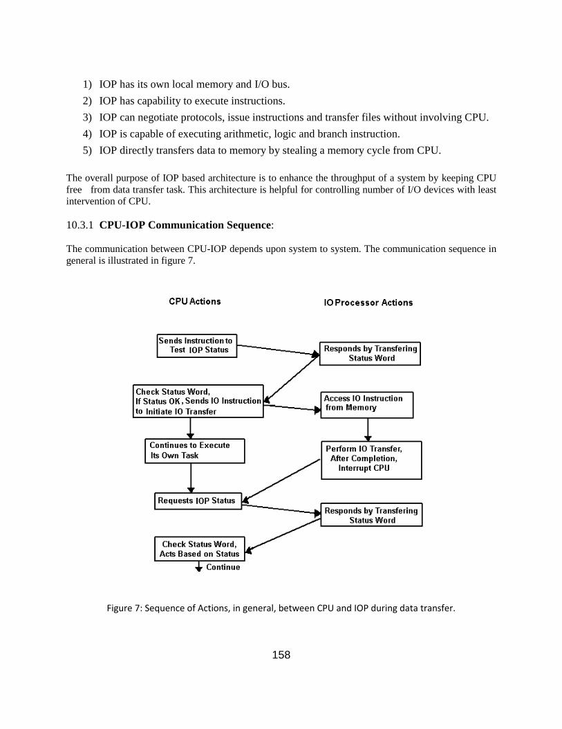
158
1) IOP has its own local memory and I/O bus.
2) IOP has capability to execute instructions.
3) IOP can negotiate protocols, issue instructions and transfer files without involving CPU.
4) IOP is capable of executing arithmetic, logic and branch instruction.
5) IOP directly transfers data to memory by stealing a memory cycle from CPU.
The overall purpose of IOP based architecture is to enhance the throughput of a system by keeping CPUfree from data transfer task. This architecture is helpful for controlling number of I/O devices with leastintervention of CPU.
10.3.1 CPU-IOP Communication Sequence:
The communication between CPU-IOP depends upon system to system. The communication sequence ingeneral is illustrated in figure 7.
Figure 7: Sequence of Actions, in general, between CPU and IOP during data transfer.

159
The CPU sends IO instruction to check IOP status. IOP responds it by transferring the status word in
memory. The CPU checks the status word and if everything is OK then sends IO instruction to IOP to
initiate IO transfer. The CPU mean time continues to execute its own task. The IOP accesses IO
instructions from memory execute them and perform IO transfer. After completing data transfer it
interrupts CPU. The CPU once again requests the IOP status and IOP responds it by transferring the
status word in memory again. CPU again checks status word and acts accordingly. In this way the entire
process of data transfer repeated again. In this way the IOP transfers data between various I/O devices and
the memory meanwhile the CPU continue to execute its own task.
10.4 Summary
The data transfer to or from memory to I/O may be transferred without involving CPU. The DMA is such
a technique which is hardware oriented. In systems where DMA controller is used to data transfer, CPU
only initiates the transfer. The technique is used for transfer data to or from memory to the high speed I/O
processor. If low speed I/O intends to communicate data using DMA, then cycle stealing technique is
used. An IOP is a processor that can communicate with I/O devices and has direct memory access
capability. The overall purpose of IOP based architecture is to enhance the throughput of a system by
keeping CPU free from data transfer task.
Check Your Progress
Q 8 : IOP is a ____________________ used to transfer data between memory and I/O device.
Answer options: a) processor b) program c) printer d) peripheral
Q 9: IOP is called as __________________________ .
Answer options: a) Input Output Program b) Input Output Processor c) Input Output Passwordd) I/O Parity
Q 10: IOP has ___________ and ________________ .
Answer options: a) no local memory, no I/O Bus b) local memory, I/O Bus c) local memory, noI/O Bus
Q 11: When IOP is busy in data transfer, the CPU ___________________
Answer options: a) Watches Data Transfer b) Helps Data Transfer c) Does Its own Task d)Does Nothing
Q 12: When IOP is busy in data transfer, the CPU ___________________
Answer options: a) Watches Data Transfer b) Helps Data Transfer c) Does Its own Task d)Does Nothing

160
10.5 Glossary
Burst Data – An I/O mode of data transfer where data is sent in blocks instead a steady stream.
Data Bus - The portion of a bus that is used to transfers data between two units.
Data Transfer Rate – The speed with which data transfer takes place between two devices.
Interrupt – An event that alters the normal control of CPU to process another job.
Interrupt Cycle – A part of the instruction cycle in which the CPU monitors the interrupt flags to check ifan interrupt is pending, and if so, invokes an interrupt-handling routine.
Peripheral Device – Peripheral is a term used for input and output.
Polling – In polling a CPU continually monitor the ports or the registers for the presence of data signal.
Status Register - A special register that monitors and records the status of various situations such asoverflow, carries, and borrows.
System Bus – An internal bus in a system that connects the CPU, memory, and all other internalcomponents.
10.6 Answer to check your progress/Suggested Answers to Questions (SAQ).
Answers to Questions: 1 to 12.
1) b 2) b 3) b 4) b 5) c 6) c
7) b 8) a 9) b 10) b 11) c 12)
10.7 References/Bibliography/Suggested Readings
Stallings, W. Computer Organization and Architecture, 8th ed., PHI Pvt, 2010. Tanenbaum, Andrew s. Structured Computer Organization, 4th ed., Pearson Education
Asia, 1999. Mano, M. Morris, Computer System Architecture, 3rd ed.,Pearson Education, Inc. Hennessy J. L., Patterson D. A., Computer Architecture, 4th ed., ELSEVIER, Reprint
2011. Hayes J. P., Computer Architecture and Organization, McGrawHill, International edition.
161
Godse A. P., Godse D.A., Computer Organization And Architecture, TechnicalPublications.
Journal of Systems Architecture: Embedded Software Design, ELSEVIER Parallel Computing, Systems and Applications, ELSEVIER ACM Transactions on Architecture and Code Optimization, ACM Journal of Parallel and Distributed Computing, Science Direct Computer Architecture Letters, IEEE Computer Society The Journal of Instruction-Level Parallelism
10.8 Terminal and Model Questions
1) What does DMA stands for? Describe its various components.
2) What is Programmed I/O mode of data transfer? Explain.
3) Differentiate between programmed I/O and interrupt driven data transfer mode.
4) Write the names of different data transfer modes.
5) Explain the role of cycle stealing in DMA.
6) Explain interrupt driven data transfer with flow diagram.
7) Draw block diagram of DMA controller and explain its working.
8) What are the advantages and applications of DMA?
9) Why IOP is required in a Computer? Explain your answer.
10) Draw block diagram of an IOP based computer system architecture.
11) Write sequence of communication between CPU and IOP.
12) Is it possible to have more than one IOP in a computer? Explain your answer.
13) Discuss CPU and IOP communication.
14) When IOP is busy in transferring data, the CPU performs which action?
15) Give a major point of distinction between cycle stealing and burst data transfer
techniques.
162
Lesson 11
Synchronous and Asynchronous Data Transfer
Structure
11.0 Objectives11.1 Introduction11.2 Synchronous and Asynchronous Data Transfer11.3 Strobe Control
11.4 Handshaking11.5 Summary11.6 Glossary11.7 Answer to check your progress/Suggested Answers to Questions (SAQ)11.8 References/ Bibliography/ Suggested Readings11.9 Terminal and Model Questions
11.0 Objectives
The main objectives of this chapter are:
To define synchronous data transfer.
To define asynchronous data transfer.
To draw and explain the block diagram of asynchronous data transfer.
To explain timing sequence in asynchronous data transfer.
To explain the strobe and handshaking techniques.
To go through the strobe control limitations.
To discuss the advantages of asynchronous data transfer
11.1 Introduction
In order to process and store data, the CPU required to communicate with I/O devices and memory. Thespeed of I/O devices is slow as compared to CPU speed. The synchronization between CPU and I/Odevices is made through a special hardware device called as an interface. In asynchronous mode of datatransfer, the registers of CPU and the registers of the device interface do not share a common clock fortiming. The main advantage of asynchronous mode is that it is flexible and efficient. In asynchronousserial transfer, the data is transmitted only if it is available on data line for transfer. Asynchronous SerialInterface is an integrated circuit that is used to receive or transmit serial data in asynchronous mode.

163
11.2 Synchronous and Asynchronous Data Transfer
The word synchronization means matching the speed of CPU with various I/O devices attached to it. Thesynchronization between various devices in a system is made using a clock pulse. The interface convertsthe signal received or transmitted on a system bus to a format that is acceptable to the I/O devices. Dataregisters are used to store data in an interface. In synchronous mode of data transfer, the registers ofCPU and the registers of the device interface share a common clock for timing i.e. both the sender andthe receiver share a common clock for timing. On the other hand, in the asynchronous mode of datatransfer, the registers of CPU and the registers of the device interface do not share a common clock fortiming i.e. each device interface has its own clock signal generator and is able to generate clock signalindependently. This causes a disparity in timing between CPU and I/O device.
The system in which each I/O device has its own clock signal generator require a common control signalthat must be transmitted between communicating devices to give the indication of initiation of datatransfer. Two techniques used for this purpose are: 1) Strobe control, 2) Handshaking.
11.3 Strobe Control
In this technique, a dedicated strobe control line is installed to indicate the data transfer time. Thestrobe may be activated or deactivated by a source or a destination device in which data transfer to takeplace. The strobe control is given in Figure 1. To start data transfer, the source device places its data (aword) on the data bus and strobe is activated by CPU being source device. The data transfer occurswhen the data bus is loaded and the stroke line is activated as given in Figure 2. Actually, stroke line isactivated after some delay after loading data so that the stability of data is maintained on the data bus.In this case, the source device is generally CPU and destination device is memory or output (writeoperation).
Figure 1: Strobe control where source activates strobe.
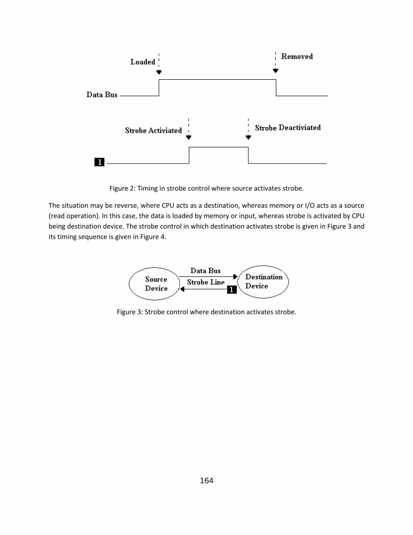
164
Figure 2: Timing in strobe control where source activates strobe.
The situation may be reverse, where CPU acts as a destination, whereas memory or I/O acts as a source(read operation). In this case, the data is loaded by memory or input, whereas strobe is activated by CPUbeing destination device. The strobe control in which destination activates strobe is given in Figure 3 andits timing sequence is given in Figure 4.
Figure 3: Strobe control where destination activates strobe.
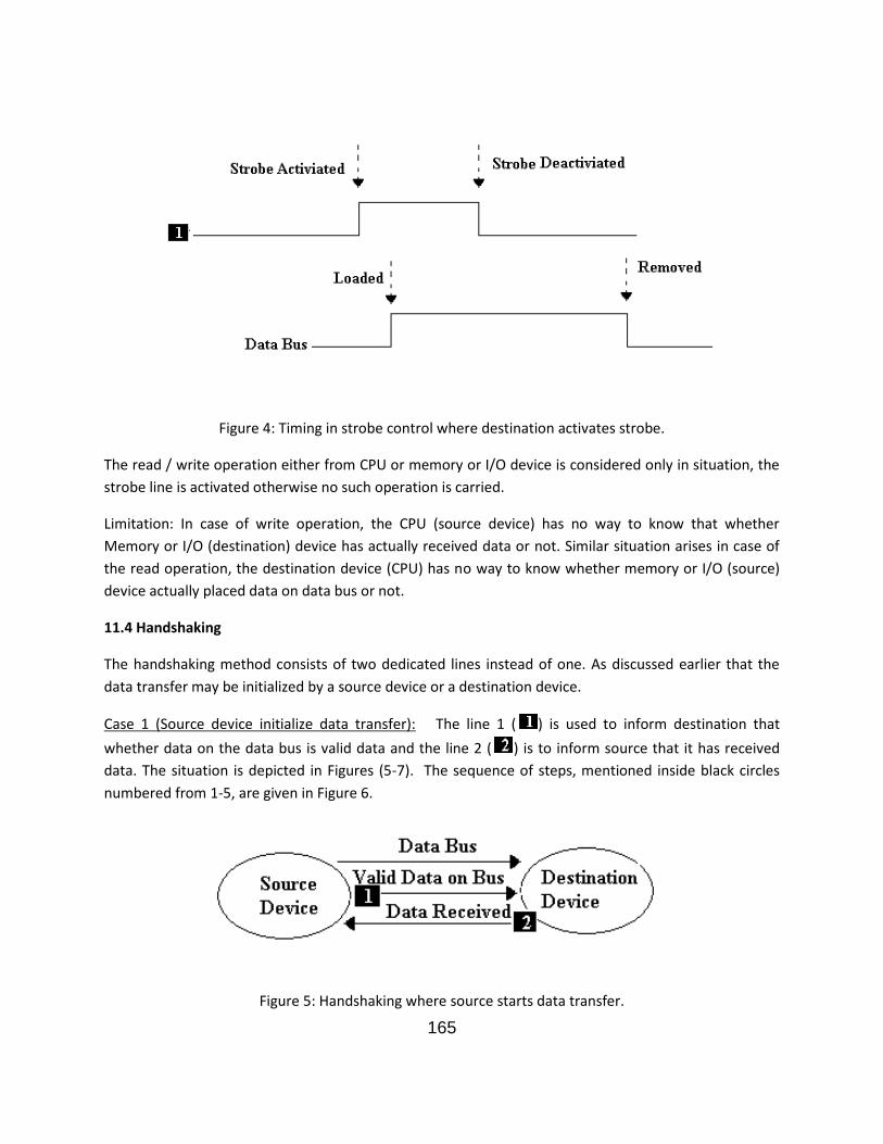
165
Figure 4: Timing in strobe control where destination activates strobe.
The read / write operation either from CPU or memory or I/O device is considered only in situation, thestrobe line is activated otherwise no such operation is carried.
Limitation: In case of write operation, the CPU (source device) has no way to know that whetherMemory or I/O (destination) device has actually received data or not. Similar situation arises in case ofthe read operation, the destination device (CPU) has no way to know whether memory or I/O (source)device actually placed data on data bus or not.
11.4 Handshaking
The handshaking method consists of two dedicated lines instead of one. As discussed earlier that thedata transfer may be initialized by a source device or a destination device.
Case 1 (Source device initialize data transfer): The line 1 ( ) is used to inform destination thatwhether data on the data bus is valid data and the line 2 ( ) is to inform source that it has receiveddata. The situation is depicted in Figures (5-7). The sequence of steps, mentioned inside black circlesnumbered from 1-5, are given in Figure 6.
Figure 5: Handshaking where source starts data transfer.
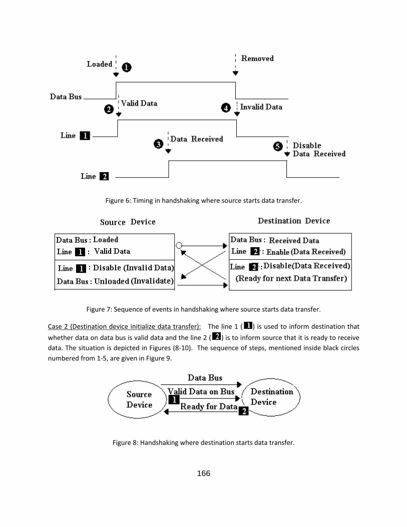
166
Figure 6: Timing in handshaking where source starts data transfer.
Figure 7: Sequence of events in handshaking where source starts data transfer.
Case 2 (Destination device initialize data transfer): The line 1 ( ) is used to inform destination thatwhether data on data bus is valid data and the line 2 ( ) is to inform source that it is ready to receivedata. The situation is depicted in Figures (8-10). The sequence of steps, mentioned inside black circlesnumbered from 1-5, are given in Figure 9.
Figure 8: Handshaking where destination starts data transfer.
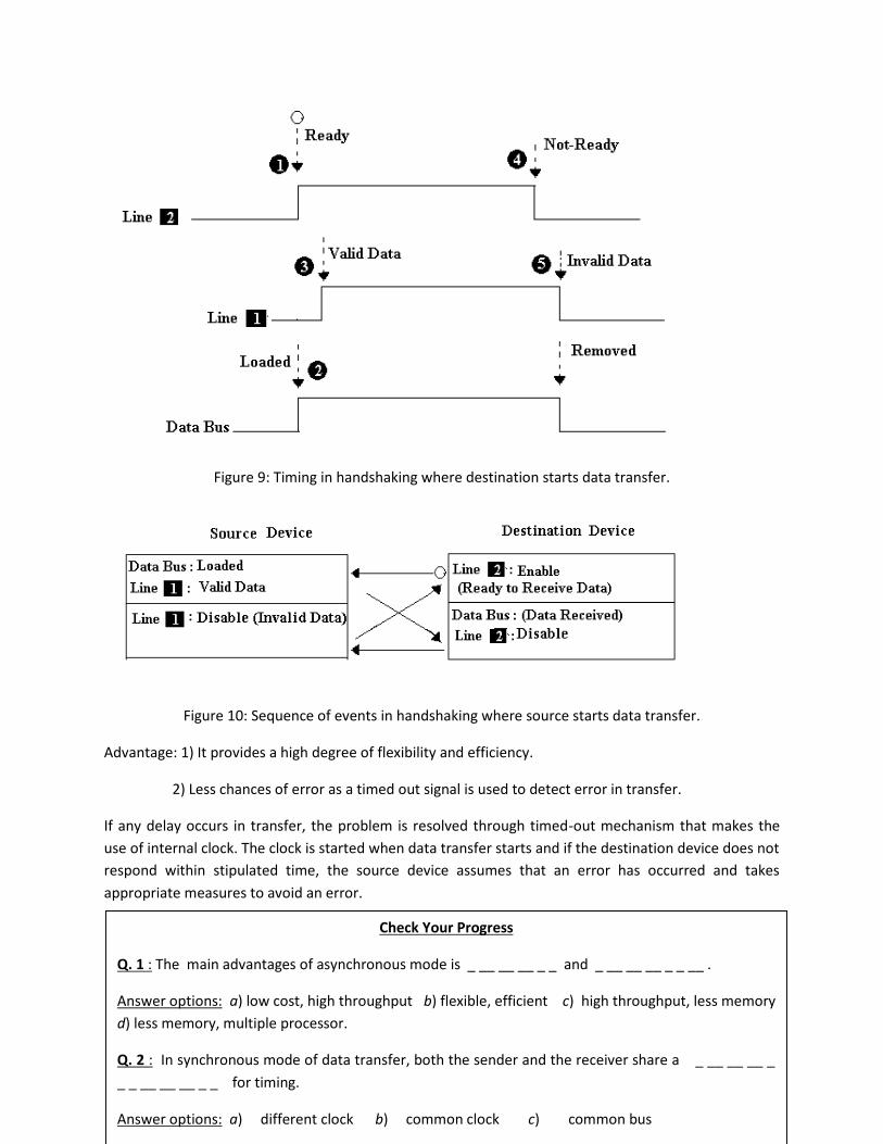
167
Figure 9: Timing in handshaking where destination starts data transfer.
Figure 10: Sequence of events in handshaking where source starts data transfer.
Advantage: 1) It provides a high degree of flexibility and efficiency.
2) Less chances of error as a timed out signal is used to detect error in transfer.
If any delay occurs in transfer, the problem is resolved through timed-out mechanism that makes theuse of internal clock. The clock is started when data transfer starts and if the destination device does notrespond within stipulated time, the source device assumes that an error has occurred and takesappropriate measures to avoid an error.
Check Your Progress
Q. 1 : The main advantages of asynchronous mode is _ __ __ __ _ _ and _ __ __ __ _ _ __ .
Answer options: a) low cost, high throughput b) flexible, efficient c) high throughput, less memoryd) less memory, multiple processor.
Q. 2 : In synchronous mode of data transfer, both the sender and the receiver share a _ __ __ __ __ _ __ __ __ _ _ for timing.
Answer options: a) different clock b) common clock c) common bus
168
11.5 Summary
In synchronous mode of data transfer, the registers of CPU and the registers of the device interfaceshare common clock. In asynchronous mode of data transfer, the registers of CPU and the registers ofthe device interface do not share a common clock for timing. The systems in which two communicatingdevice have their private clock signal generator either use strobe or handshaking technique to makeparity between steps.
11.6 Glossary
Data Bus - The portion of a bus that is used to transfer the data between two units.
Parallel Communication - Communication in which an entire byte (or word) is transmittedat the same time over the communication medium.
System Bus - A bus used to communicate between CPU, memory and I/O.
Serial Communication - A method of transmitting data where a data byte is sent one bit at a time overthe communication medium. Serial communication is asynchronous.Status Register - A special register that monitors and records the status of various situations such asoverflow, carries, borrows, etc.
169
11.7 Answer to check your progress/Suggested Answers to Questions (SAQ)
Answers to Questions: 1 to 5.
1) b 2) b 3) b 4) b
5) a
11.8 References/Bibliography/ Suggested Readings
Stallings, W. Computer Organization and Architecture, 8th ed., PHI Pvt, 2010. Tanenbaum, Andrew s. Structured Computer Organization, 4th ed., Pearson Education
Asia, 1999. Mano, M. Morris, Computer System Architecture, 3rd ed.,Pearson Education, Inc. Hennessy J. L., Patterson D. A., Computer Architecture, 4th ed., ELSEVIER, Reprint
2011. Hayes J. P., Computer Architecture and Organization, McGrawHill, International edition. Rajaraman V., Radhakrishnan, Computer Organization and Architecture, PHI, 2007. Hennessy J. L., Patterson D. A., Computer Organization and Design, ELSEVIER, 2012. Godse A. P., Godse D.A., Computer Organization And Architecture, Technical
Publications. Journal of Systems Architecture: Embedded Software Design, ELSEVIER Parallel Computing, Systems and Applications, ELSEVIER ACM Transactions on Architecture and Code Optimization, ACM Journal of Parallel and Distributed Computing, Science Direct Computer Architecture Letters, IEEE Computer Society The Journal of Instruction-Level Parallelism
11.9 Terminal and Model Questions
16) What is synchronous data transfer? Explain.
17) What is asynchronous data transfer? Explain.
18) Differentiate between synchronous and asynchronous data transfer.
19) Explain the role of strobe control and handshaking in asynchronous data transfer.
20) What are the limitations of strobe control in asynchronous data transfer?
21) Write down some advantages of handshaking.
22) Write sequence of events in handshaking where source starts data transfer.
170
23) Explain timing sequence in handshaking where destination starts data transfer.
24) Discuss handshaking technique where destination device initialize data transfer.
25) Discuss handshaking technique where source device initialize data transfer.
26) Differentiate between handshaking and strobe.
171
Lesson 12
Stack Organization
Structure
12.0 Objectives
12.1 Introduction
12.2 Stack Organization
12.3 Type of stacks
12.3.1 Register stack
12.3.2 Memory stack
12.4 Application of stack
12.5 Summary
12.6 Glossary
12.7 Answer to Check Your Progress/Suggested Answers to SAQ
12.8 Bibliography/References/Suggested Readings
12.9 Terminal and Model Questions
12.0 Objectives
After studying this chapter you will understand
The problems related to stack organization.
Different types of stacks.
Implementation of the stacks.
Insertion and deletion in the stack.
Application of stack in arithmetic expression.
12.1 Introduction
Stack is a storage structure that is used to store the temporary data during the computations. It is based onthe principle LIFO i.e. the last item stored is the first item to be retrieved. Stack uses a register named, stack
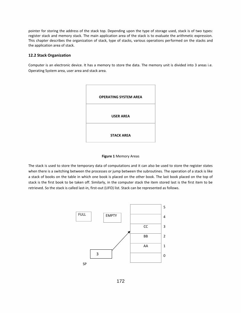
172
pointer for storing the address of the stack top. Depending upon the type of storage used, stack is of two types:register stack and memory stack. The main application area of the stack is to evaluate the arithmetic expression.This chapter describes the organization of stack, type of stacks, various operations performed on the stacks andthe application area of stack.
12.2 Stack Organization
Computer is an electronic device. It has a memory to store the data. The memory unit is divided into 3 areas i.e.Operating System area, user area and stack area.
Figure 1 Memory Areas
The stack is used to store the temporary data of computations and it can also be used to store the register stateswhen there is a switching between the processes or jump between the subroutines. The operation of a stack is likea stack of books on the table in which one book is placed on the other book. The last book placed on the top ofstack is the first book to be taken off. Similarly, in the computer stack the item stored last is the first item to beretrieved. So the stack is called last-in, first-out (LIFO) list. Stack can be represented as follows.
SP
OPERATING SYSTEM AREA
USER AREA
STACK AREA
5
4
CC 3
BB 2
AA 1
0
FULL EMPTY
3

173
Figure 2: Stack Organization
The figure 2 shows the stack organization. The stack is consisting of memory unit, Stack Pointer (SP) register, FlipFlops: FULL and EMPTY. The stack pointers always points towards the top of the stack. When a new item is addedto the stack the SP increases by one. The FULL and EMPTY is 1 bit flip flop and is used to tell whether the stack isfull or empty.
The two operations, insertion and deletion are used for accessing the data within the stack. The insertion operationis also called PUSH operation. In this new item is added into the stack. The operation of deletion is called POPoperation. In this operation an item is removed from the stack. These two operations can be simulated byincrementing and decrementing the stack pointer (SP) value.
For example, in figure 2, the SP value is 3. We want to push DD into the stack. After the PUSH operation the newvalue of SP will be 4. When the pop DD operation is done then again the SP value become 3. Further we want topop BB from the stack then perform pop CC followed by pop BB. Now the SP value becomes 1.
12.3 Type of stacks
There are two types of stacks
1. Register Stack
2. Memory Stack
12.3.1 Register Stack
The register stack can be organized as the collection of finite number of registers or the memory words. Figure 3shows the register stack of 64-words. The total number of bits required to give the addresses of registers are 6because 26=64. The SP register contain the binary value of 6 bit to store the address of stack top. In the figure 3 thestack top address is 4 (i.e. 000101).
63
CC 3
BB 2
AA 1
0
FULL EMPTY
SP
DR
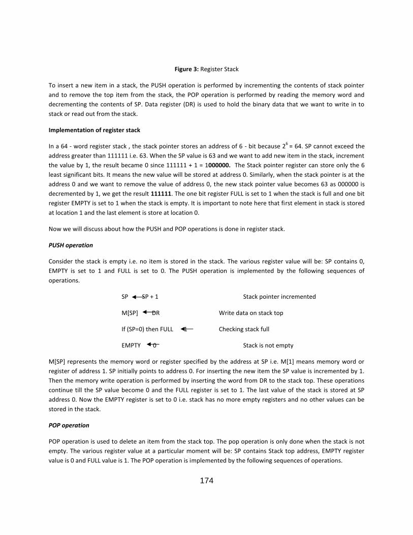
174
Figure 3: Register Stack
To insert a new item in a stack, the PUSH operation is performed by incrementing the contents of stack pointerand to remove the top item from the stack, the POP operation is performed by reading the memory word anddecrementing the contents of SP. Data register (DR) is used to hold the binary data that we want to write in tostack or read out from the stack.
Implementation of register stack
In a 64 - word register stack , the stack pointer stores an address of 6 - bit because 26 = 64. SP cannot exceed theaddress greater than 111111 i.e. 63. When the SP value is 63 and we want to add new item in the stack, incrementthe value by 1, the result became 0 since 111111 + 1 = 1000000. The Stack pointer register can store only the 6least significant bits. It means the new value will be stored at address 0. Similarly, when the stack pointer is at theaddress 0 and we want to remove the value of address 0, the new stack pointer value becomes 63 as 000000 isdecremented by 1, we get the result 111111. The one bit register FULL is set to 1 when the stack is full and one bitregister EMPTY is set to 1 when the stack is empty. It is important to note here that first element in stack is storedat location 1 and the last element is store at location 0.
Now we will discuss about how the PUSH and POP operations is done in register stack.
PUSH operation
Consider the stack is empty i.e. no item is stored in the stack. The various register value will be: SP contains 0,EMPTY is set to 1 and FULL is set to 0. The PUSH operation is implemented by the following sequences ofoperations.
SP SP + 1 Stack pointer incremented
M[SP] DR Write data on stack top
If (SP=0) then FULL 1 Checking stack full
EMPTY 0 Stack is not empty
M[SP] represents the memory word or register specified by the address at SP i.e. M[1] means memory word orregister of address 1. SP initially points to address 0. For inserting the new item the SP value is incremented by 1.Then the memory write operation is performed by inserting the word from DR to the stack top. These operationscontinue till the SP value become 0 and the FULL register is set to 1. The last value of the stack is stored at SPaddress 0. Now the EMPTY register is set to 0 i.e. stack has no more empty registers and no other values can bestored in the stack.
POP operation
POP operation is used to delete an item from the stack top. The pop operation is only done when the stack is notempty. The various register value at a particular moment will be: SP contains Stack top address, EMPTY registervalue is 0 and FULL value is 1. The POP operation is implemented by the following sequences of operations.

175
DR M[SP] Read stack top
SP SP-1 Decrements stack pointer
If (SP=0) then EMPTY 1 Checking if stack empty
FULL 0 Stack is not full
In the above micro operations the top item is read from the stack in to the Data register (DR). The value of stackpointer is then decremented. If the SP value reaches zero, then the stack gets empty and so EMPTY register is setto 1 and FULL register is set to 0.
Figure 4: Register Stack (Full) Figure 5: Register Stack (Empty)
Figure 4 represents the condition when the stack is completely filled. So the first item to be popped out in thiscondition is of address 0 i.e. DR M [0]. Now the SP is decremented by 1 i.e. 000000-1, and the result is 111111(means 63). This result we get is by adding 2’s complement of 1 with 000000. Then the next item is popped from63, 62, 61 and so on up to 1. The last item is popped out from location 1 and SP is decremented to 0. Now thestack is empty as shown in Figure 5. Register EMPTY set to 1 and FULL set to 0.
The above two operations i.e. push and pop can be used for register stack only as stack grows by increasing theaddress of register stack.
Self Assessment 1
Q1. Define stack. What are the various functions of stack?
Sol. __________________________________________________________________________
__________________________________________________________________________
YY 63
: :
CC 3
BB 2
AA 1
ZZ 0
63
:
3
2
1
0
DR DR
SP
P
SP
P
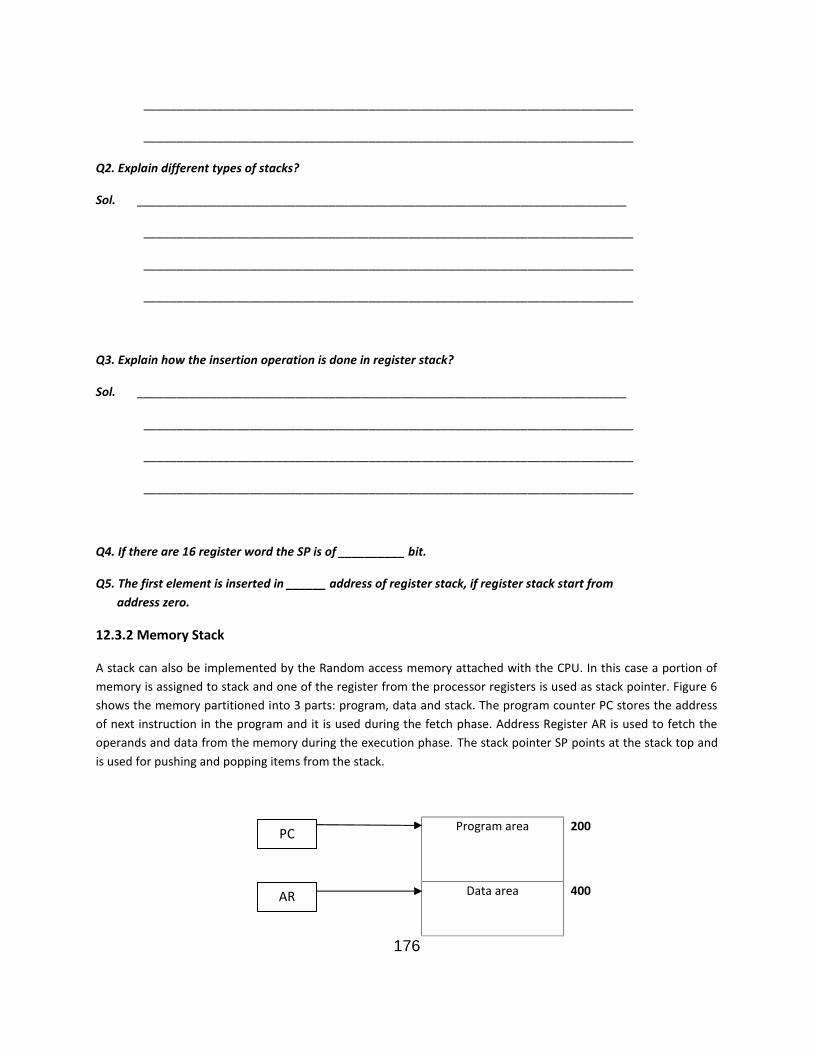
176
__________________________________________________________________________
__________________________________________________________________________
Q2. Explain different types of stacks?
Sol. __________________________________________________________________________
__________________________________________________________________________
__________________________________________________________________________
__________________________________________________________________________
Q3. Explain how the insertion operation is done in register stack?
Sol. __________________________________________________________________________
__________________________________________________________________________
__________________________________________________________________________
__________________________________________________________________________
Q4. If there are 16 register word the SP is of __________ bit.
Q5. The first element is inserted in ______ address of register stack, if register stack start fromaddress zero.
12.3.2 Memory Stack
A stack can also be implemented by the Random access memory attached with the CPU. In this case a portion ofmemory is assigned to stack and one of the register from the processor registers is used as stack pointer. Figure 6shows the memory partitioned into 3 parts: program, data and stack. The program counter PC stores the addressof next instruction in the program and it is used during the fetch phase. Address Register AR is used to fetch theoperands and data from the memory during the execution phase. The stack pointer SP points at the stack top andis used for pushing and popping items from the stack.
Program area 200
Data area 400
PC
PAR
P

177
Stack area
600
800
Figure 6: Memory unit with stack
The initial value of SP is 800 as shown in figure 6. Thus the first item is stored at address 799 and the last value ofstack is 600. Data register DR performs the same operation in memory stack as it does in register stack.
PUSH operation
The new item is inserted with the push operation in the stack. Since the memory address decreases in stack as itgrows, we need to decrement the SP to get the next address in the stack. Then the memory write operation insertsthe word into the stack
SP SP - 1
M [SP] DR
POP operation
DR M [SP]
SP SP +1
In the pop operation the top item is read from the stack into the DR. The stack pointer is then incremented topoint to new stack top.
Here we do not get the hardware to check stack full or stack empty. Stack full is also called stack overflow andstack empty is also called stack underflow. For checking the stacks overflow or stack underflow the two processorregisters are used. First register holds the upper limit of stack i.e. 600 and other register holds the lower limit i.e.800. After the push operation SP is compared with the upper limit register and after pop operation it is comparedto lower limit register.
12.4 Application of Stack
Stacks are very useful in evaluating the arithmetic operations. The arithmetic expressions are written in reversepolish notation in the stack. Let us first study the different representations of expression.
DR
SP
P
P
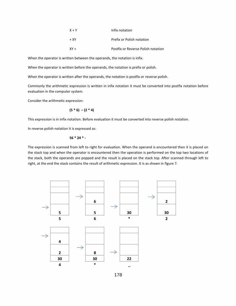
178
X + Y Infix notation
+ XY Prefix or Polish notation
XY + Postfix or Reverse Polish notation
When the operator is written between the operands, the notation is infix.
When the operator is written before the operands, the notation is prefix or polish.
When the operator is written after the operands, the notation is postfix or reverse polish.
Commonly the arithmetic expression is written in infix notation it must be converted into postfix notation beforeevaluation in the computer system.
Consider the arithmetic expression:
(5 * 6) – (2 * 4)
This expression is in infix notation. Before evaluation it must be converted into reverse polish notation.
In reverse polish notation it is expressed as:
56 * 24 * -
The expression is scanned from left to right for evaluation. When the operand is encountered then it is placed onthe stack top and when the operator is encountered then the operation is performed on the top two locations ofthe stack, both the operands are popped and the result is placed on the stack top. After scanned through left toright, at the end the stack contains the result of arithmetic expression. It is as shown in figure 7.
6 2
5 5 30 305 6 * 2
4
2 830 30 224 * _
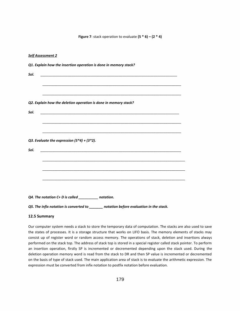
179
Figure 7: stack operation to evaluate (5 * 6) – (2 * 4)
Self Assessment 2
Q1. Explain how the insertion operation is done in memory stack?
Sol. ______________________________________________________________________
_______________________________________________________________________
_______________________________________________________________________
Q2. Explain how the deletion operation is done in memory stack?
Sol. _______________________________________________________________________
_______________________________________________________________________
_______________________________________________________________________
Q3. Evaluate the expression (5*4) + (3*2).
Sol. ________________________________________________________________________
_________________________________________________________________________
_________________________________________________________________________
_________________________________________________________________________
Q4. The notation C+ D is called __________ notation.
Q5. The infix notation is converted to _______ notation before evaluation in the stack.
12.5 Summary
Our computer system needs a stack to store the temporary data of computation. The stacks are also used to savethe states of processes. It is a storage structure that works on LIFO basis. The memory elements of stacks mayconsist up of register word or random access memory. The operations of stack, deletion and insertions alwaysperformed on the stack top. The address of stack top is stored in a special register called stack pointer. To performan insertion operation, firstly SP is incremented or decremented depending upon the stack used. During thedeletion operation memory word is read from the stack to DR and then SP value is incremented or decrementedon the basis of type of stack used. The main application area of stack is to evaluate the arithmetic expression. Theexpression must be converted from infix notation to postfix notation before evaluation.
180
12.6 Glossary
Address Register: Address Register (AR) is used to fetch the operands and data from the memory duringthe execution phase.
EMPTY: It is 1 bit register and is set to 1 when the stack is empty. FULL: It is 1 bit register and is set to 1 when the stack is full. Infix notation: It is a notation for arithmetic expression in which operator is placed in between the
operands. Pop operation: Pop operation is used to remove the data from the stack top. Postfix notation: It is a notation for arithmetic expression in which operator is placed after the operands.
It is also called reverse polish notation. Prefix notation: It is a notation for arithmetic expression in which operator is placed before the operands.
It is also called polish notation. Program Counter: The program counter (PC) stores the address of next instruction in the program and it
is used during the fetch phase. Push operation: Push operation is used to insert data in to the stack top. In case of register stack, SP is
incremented first to insert the data on the stack top. Stack: Stack is a storage device that stores information in Last in First out (LIFO) basis. It can be compared
to the stack of tray or stack of books. Stack Pointer: stack pointer is a special type of register that stores the address of stack top.
12.7 Answer to Check Your Progress/Suggested Answers to SAQ
Self Assessment 1
Solution 1) A stack is storage device that stores the information in last in first out mode. It is used to storetemporary data of computation and also used to store the states of various processor register during switchingamong the processes. Further the stacks are used to evaluate the arithmetic equations..Solution 2) There are two types of tacks register stack and memory stack. The register stack is consisting up ofregisters and memory stack is consisting up of random access memory. Stack pointer is used to store the addressof the stack top. Register stacks grows with increasing the address where as memory stack is grow with decreasingthe memory address.
Solution 3) SP SP + 1
M[SP] DR
If (SP=0) then FULL 1
EMPTY 0
.first of all the stack pointer value is incremented by 1 then value from the data register is stored in the stack. Thisprocess is continue till the value of SP become 0 and FULL register is set to 1 and EMPTY register is set 0.

181
Solution 4) 4 - Bits
Solution 5) first
Self Assessment 2
Solution 1) The new item is inserted with the push operation in the stack. Since the memory address decreases instack as it grows, we need to decrement the SP to get the next address in the stack. Then the memory writeoperation inserts the word into the stack
SP SP - 1
M [SP] DR
Solution 2) In the memory stack the deletion operation is done with the help of pop operation. In this operationthe top item is read from the stack into the DR. The stack pointer is then incremented to point to new stack top
DR M [SP]
SP SP +1
Solution 3) The postfix notation will be 54* 32* +. When the expression is scanned from left to right operand 5 isstore in the stack and then operand 4 is store on the stack top. The operator * do the multiplication of the top twomemory location. The result we get i.e. 20 is store in the stack. Similarly the result of multiplication of 3 and 2 i.e. 6is store on the stack top. At the end, the operator + is encounter, it do the addition of top two locations of stackand the result is store in the stack. We get the result 26.
Solution 4) Infix
Solution 5) Postfix
12.8 Bibliography/References/ Suggested Readings
1. Computer System Architecture, M.M. Mano, Third Edition, PHI2. Computer Organization and Architecture Lab.3. Computer Organization and Architecture, Stallings, Eighth Edition, PHI
12.9 Terminal and Model Questions
Q1. What are stacks? Explain different types of stacks
Q2. Why we use stack?
Q3. Differentiate between memory stacks and register stacks?
Q4. What is the role of stack pointer and data register in stack organization?

182
Q5. Explain why the zeros location is filled in last?
Q6. Explain the state of stack when FULL = 1 and EMPTY =0.
Q7. Explain the state of stack when FULL = 0 and EMPTY =1.
Q8. Write a note on push and pop operations.
183
Lesson 13
Memory Organization
Structure
13.0 Objectives
13.1 Introduction
13.2 Memory Hierarchy
13.3 Main memory/ Primary Memory
13.4 RAM (Random Access Memory)
13.4.1 RAM Chip
13.5 ROM (Read Only Memory)
13.5.1 ROM Chip
13.6 Logical and Physical Address
13.7 Memory Address Map
13.8 Memory Connection to CPU
13.9 Associative Memory
13.9.1 Hardware Organization
13.10 Summary
13.11 Glossary
13.12 References/Bibliography/Suggested Readings
13.13 Terminal and Model Questions
13.0 Objectives
After reading this chapter students will be able to understand
Memory Hierarchy Main Memory RAM RAM Chip ROM ROM Chip Logical and Physical Address Memory Address Map Memory connection to CPU Associative Memory
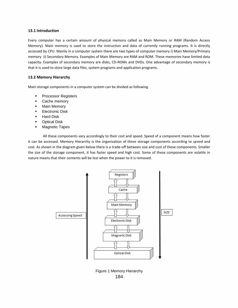
184
13.1 Introduction
Every computer has a certain amount of physical memory called as Main Memory or RAM (Random AccessMemory). Main memory is used to store the instruction and data of currently running programs. It is directlyaccessed by CPU. Mainly in a computer system there are two types of computer memory i) Main Memory/Primarymemory ii) Secondary Memory. Examples of Main Memory are RAM and ROM. These memories have limited datacapacity. Examples of secondary memory are disks, CD-ROMs and DVDs. One advantage of secondary memory isthat it is used to store large data files, system programs and application programs.
13.2 Memory Hierarchy
Main storage components in a computer system can be divided as following
Processor Registers Cache memory Main Memory Electronic Disk Hard Disk Optical Disk Magnetic Tapes
All these components vary accordingly to their cost and speed. Speed of a component means how fasterit can be accessed. Memory Hierarchy is the organization of these storage components according to speed andcost. As shown in the diagram given below there is a trade-off between size and cost of these components. Smallerthe size of the storage component, it has faster speed and high cost. Some of these components are volatile innature means that their contents will be lost when the power to it is removed.
Figure 1 Memory Hierarchy
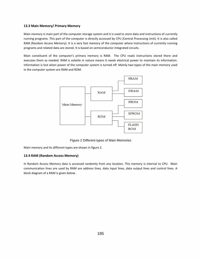
185
13.3 Main Memory/ Primary Memory
Main memory is main part of the computer storage system and it is used to store data and instructions of currentlyrunning programs. This part of the computer is directly accessed by CPU (Central Processing Unit). It is also calledRAM (Random Access Memory). It is a very fast memory of the computer where instructions of currently runningprograms and related data are stored. It is based on semiconductor integrated circuits.
Main constituent of the computer's primary memory is RAM. The CPU reads instructions stored there andexecutes them as needed. RAM is volatile in nature means it needs electrical power to maintain its information.Information is lost when power of the computer system is turned off. Mainly two types of the main memory usedin the computer system are RAM and ROM.
Figure 2 Different types of Main Memories
Main memory and its different types are shown in figure 2.
13.4 RAM (Random Access Memory)
In Random Access Memory data is accessed randomly from any location. This memory is internal to CPU. Maincommunication lines are used by RAM are address lines, data input lines, data output lines and control lines. Ablock diagram of a RAM is given below.
186
Figure 3 Block diagram of RAM
As shown in the figure 3, data is stored into the RAM memory through n-data input lines. Requested data /desireddata is supplied by n-data output lines. The k-address lines are used by RAM to give a binary number address. Mainoperations performed by random access memory are read and write operations through read and write controlsignals. Main steps which are used to store data in the RAM are (i) First binary address is applied to the addresslines (ii) Data bits are applied into the data input lines iii) The write signal is activated . While reading data frommain memory main steps are: (i) Binary address is applied into the address lines (ii) Read input is then activated,Memory unit then take the selected data and send them to the output lines.
13.4.1 RAM Chip
A RAM chip consists of following components:
i) One or more control inputs lines to select a chip
ii) A bidirectional data bus: It is used to transfer data from memory to CPU and from CPU to memory.
iii) Read and write input lines for specifying whether it is read operation or write operation
iv) Address line
A block diagram of a RAM chip of capacity 128 8 is shown in figure 4. It consists of 128 words and each wordconsists of 8 bits. It requires 7-bit address since 128 = 27, 8-bit bidirectional data bus, two chip select (CS) control
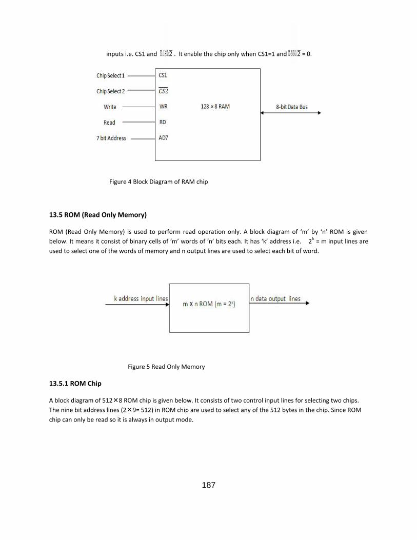
187
inputs i.e. CS1 and CS2 . It enable the chip only when CS1=1 and CS2 = 0.
Figure 4 Block Diagram of RAM chip
13.5 ROM (Read Only Memory)
ROM (Read Only Memory) is used to perform read operation only. A block diagram of ‘m’ by ‘n’ ROM is givenbelow. It means it consist of binary cells of ‘m’ words of ‘n’ bits each. It has ‘k’ address i.e. 2k = m input lines areused to select one of the words of memory and n output lines are used to select each bit of word.
Figure 5 Read Only Memory
13.5.1 ROM Chip
A block diagram of 5128 ROM chip is given below. It consists of two control input lines for selecting two chips.The nine bit address lines (29= 512) in ROM chip are used to select any of the 512 bytes in the chip. Since ROMchip can only be read so it is always in output mode.

188
Figure 6 ROM chip of capacity 512 × 8
13.6 Logical and Physical Address
Physical address is the actual address in the memory and logical address is the address generated by the CPU. Setof such actual address space values is called memory space. Set of logical address space values is called addressspace. Logical address can be of fixed size or it can be of variable length. If it is of fixed size then it is also calledvirtual address.
13.7 Memory Address Map
A memory address map is a tabular representation of address space for each chip (RAM and/or ROM) in thecomputer system. For example suppose requirement of a computer system is 512 bytes of RAM and 512 bytes ofROM. So in this example a total of 1024= 210 bytes of memory is considered. The tabular representation of memoryaddress map for this example is shown in figure 7 given below. The component column tells whether a RAM chipor ROM chip is used. The address line number 10 is used to distinguish whether it is a RAM chip or it is a ROM chipand address lines 9 and 8 are used to select between the four RAM chips. When address bit is 0 in line 10, thenCPU selects a RAM chip and when it is equal to 1, then CPU selects the ROM chip. The hexadecimal address columncontains a range of hexadecimal addresses for each RAM chip and ROM chip in the computer system.

189
Figure 7 Memory Address Map
13.8 Memory Connection to CPU
Both chips RAM and ROM in a computer system are connected to CPU through the data and address bus. Loworder address bus lines are used to select the requested or desired data present within the chips and other addressbus lines are used select a particular chip. A diagram showing memory connection to CPU is shown in figure 8given below. As shown in the diagram each RAM chip receives the 7 low-order bits of the address bus. A 2 × 4decoder is used to select a particular RAM chip. The RD and WR output lines from the CPU are applied to inputs ofeach RAM chip. Bus line 10 selects between a RAM chip and ROM chip. Address lines 1 to 9 go directly to AD9 linesof ROM chip.
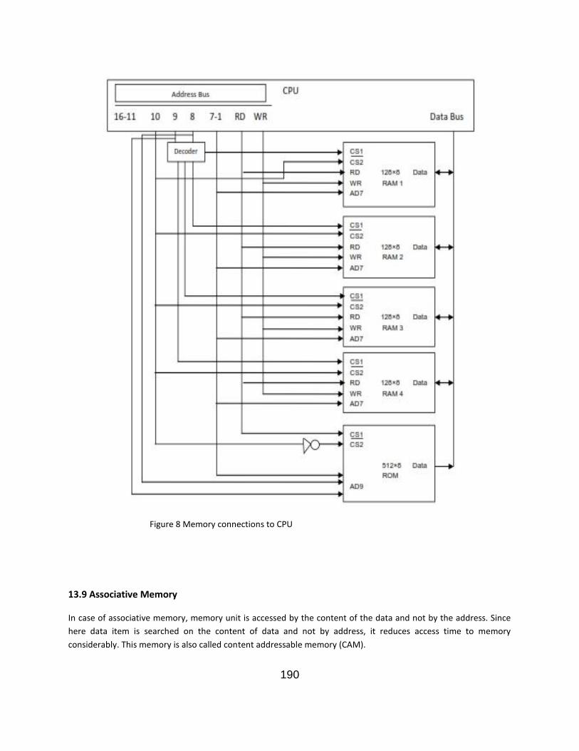
190
Figure 8 Memory connections to CPU
13.9 Associative Memory
In case of associative memory, memory unit is accessed by the content of the data and not by the address. Sincehere data item is searched on the content of data and not by address, it reduces access time to memoryconsiderably. This memory is also called content addressable memory (CAM).
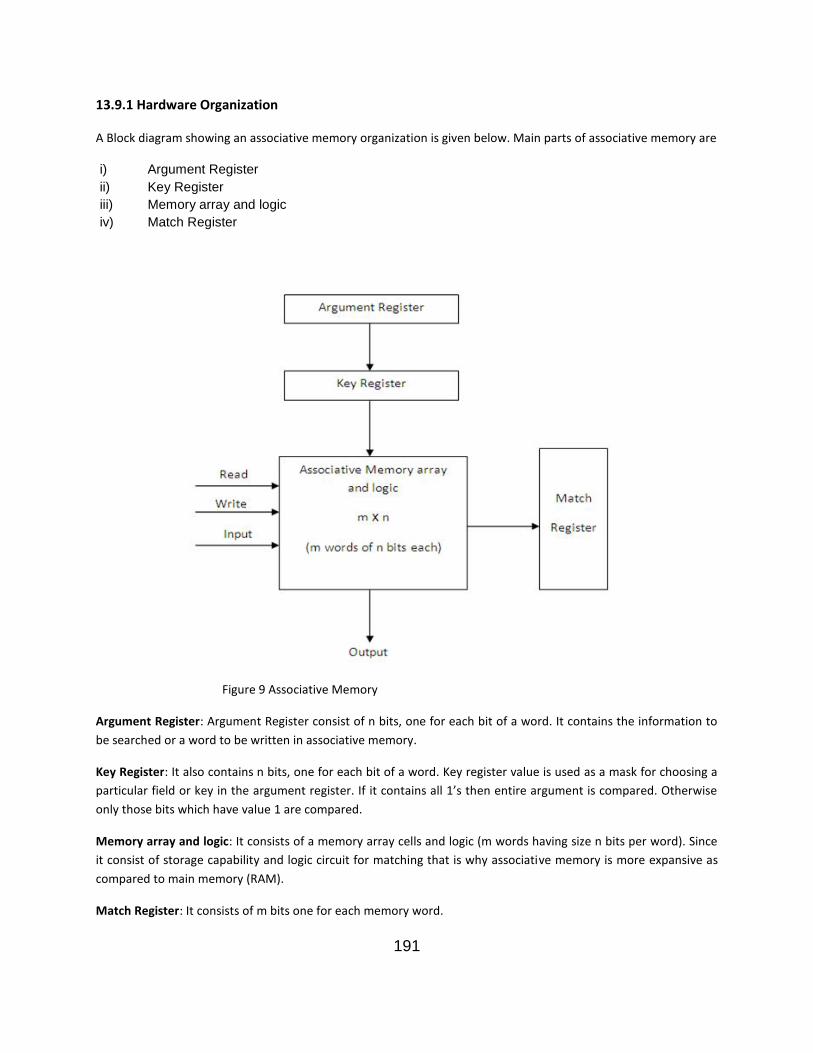
191
13.9.1 Hardware Organization
A Block diagram showing an associative memory organization is given below. Main parts of associative memory are
i) Argument Registerii) Key Registeriii) Memory array and logiciv) Match Register
Figure 9 Associative Memory
Argument Register: Argument Register consist of n bits, one for each bit of a word. It contains the information tobe searched or a word to be written in associative memory.
Key Register: It also contains n bits, one for each bit of a word. Key register value is used as a mask for choosing aparticular field or key in the argument register. If it contains all 1’s then entire argument is compared. Otherwiseonly those bits which have value 1 are compared.
Memory array and logic: It consists of a memory array cells and logic (m words having size n bits per word). Sinceit consist of storage capability and logic circuit for matching that is why associative memory is more expansive ascompared to main memory (RAM).
Match Register: It consists of m bits one for each memory word.
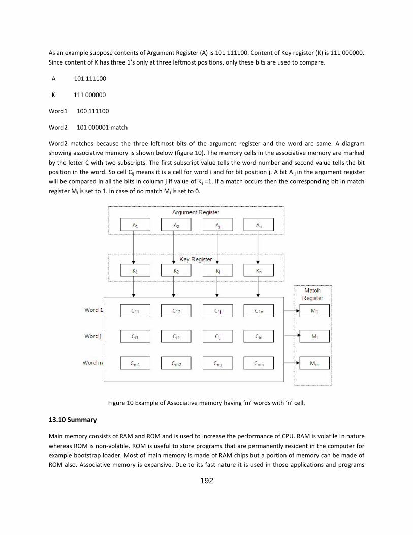
192
As an example suppose contents of Argument Register (A) is 101 111100. Content of Key register (K) is 111 000000.Since content of K has three 1’s only at three leftmost positions, only these bits are used to compare.
A 101 111100
K 111 000000
Word1 100 111100
Word2 101 000001 match
Word2 matches because the three leftmost bits of the argument register and the word are same. A diagramshowing associative memory is shown below (figure 10). The memory cells in the associative memory are markedby the letter C with two subscripts. The first subscript value tells the word number and second value tells the bitposition in the word. So cell Cij means it is a cell for word i and for bit position j. A bit A j in the argument registerwill be compared in all the bits in column j if value of Kj =1. If a match occurs then the corresponding bit in matchregister Mi is set to 1. In case of no match Mi is set to 0.
Figure 10 Example of Associative memory having ‘m’ words with ‘n’ cell.
13.10 Summary
Main memory consists of RAM and ROM and is used to increase the performance of CPU. RAM is volatile in naturewhereas ROM is non-volatile. ROM is useful to store programs that are permanently resident in the computer forexample bootstrap loader. Most of main memory is made of RAM chips but a portion of memory can be made ofROM also. Associative memory is expansive. Due to its fast nature it is used in those applications and programs

193
where the search time is very short. Main application areas of associative memory are database engines, artificialneural networks and intrusion prevention systems.
13.11 GlossaryAccess Time: It is the speed of memory measured in nano - seconds.
Array: It is that area of the RAM that is used to store the bits.
Auxiliary Memory: Devices that are used for backup storage are called auxiliary memory. For example magneticdisks.
Bidirectional Bus: A bus is called Bi-directional bus if the same bus is used for transfer of data between CPU andmemory or input / output devices in both the direction.
Bootstrap Loader: Bootstrap loader is a program that resides in the computer's ROM and is used to start thecomputer's operating system when the power is turned on.
CAM: Content Addressable Memory
Refresh Rate: It is the speed with which DRAM is refreshed. Refresh Rate refers the size of data that must berecharged.
13.12 References/Bibliography/Suggested Readings
1. Mano, M.M., Computer System Architecture, 3rd ed., PHI..
2. Mano, M.M: Digital Logic and Computer Design, Prentice Hall of India.3. Stalling, W, Computer Organization and Architecture, 8th ed., PHI.4. Hayes: Computer Architecture and Organization, McGraw-Hill International Edition.5. Tanenbaum, A.S., Structured Computer Organization 5th ed., Prentice Hall of India13.13 Terminal and Model Questions
Q.1. How many address bus lines must be used to access 2048 bytes of memory?
Ans: Since 211 = 2048 So 11 address lines are used.
Q.2. How many 128 x 8 RAM chips are needed to provide a memory capacity of 2048 bytes?
Ans: 16 Chips
Q.3. What are the main constituents of associative memory. Why associative memory is faster than othermemories?
Q.4. What are the advantages and disadvantages of associative memory?
Q.5. Draw the logic diagram of all cells along one vertical column in an associative memory.
Q.6. Describe how multiple matched words can be read out from an associative memory?
Q.7. Describe memory connection to CPU with one example.
194
CHAPTER 14
Cache Memory
Structure
14.0 Objectives
14.1 Introduction
14.2 Cache Memory
14.3 Working of Cache
14.4 Cache Initialization
14.5 Writing into Cache
14.6 Write through method
14.7 Write Back method
14.8 Replacement Algorithms
14.9 Summary
14.10 Glossary
14.11 Terminal and Model Questions
14.12 References/Bibliography/Suggested Readings
14.0 Objectives
The basic concept of Cache memory. Working of Cache Different levels of Cache Hit ratio Writing into Cache (Write-through method) Writing into Cache (Write-back method) Locality of Reference Replacement Algorithms
195
14.1 INTRODUCTION
Cache memory is a high speed memory as compared to main memory and it is availablebetween the CPU and main memory. It is small in size and expansive as compared to mainmemory. Main function of cache memory is to speed up the access time of data andinstructions stored in main memory. Without cache memory CPU has to wait while fetchingdata and instructions from the main memory.
14.2 Cache Memory
CPU access main memory and registers built into the processor directly. These registers arevery fast and can be accessed within one cycle of the CPU clock. Nowadays modern CPUs candecode instruction and can perform operations on the register content at the rate of one ormore operations per clock tick. But main memory access speed is less as compared to theseregisters, means main memory is accessed slowly. So normally CPU waits, since it does not havethe sufficient data to complete the instruction. Therefore speed of the CPU is depending on thespeed of the main memory. The solution is to add fast memory between CPU and primarymemory. This high speed memory is called cache memory. Cache memory is very high speedmemory used to increase the speed of processing by making the current program instructionsand data available to CPU at a very high rate. So cache is a technique which is used tocompensate the mismatch of speeds of CPU and primary memory. Cache is used to store thoseparts of the programs that are currently running. It is also used to store temporary data used bythese programs for calculation. So with the help of this technique it is possible to increase theperformance rate of the computer.
14.3 Working of Cache
When the CPU needs to access memory first cache is examined. If the required word is found inthe cache then it is read from the cache. If the required word is not found in the cache thenmain memory is accessed to read the word. At the same time the block of the words containingthe one just accessed is then transferred from main memory to cache memory. In this waysome amount of data from main memory is transferred to cache memory so that futurereference to same data (phenomenon of locality of reference) can be accessed from Cachememory. Figure 1 given below shows single level cache.
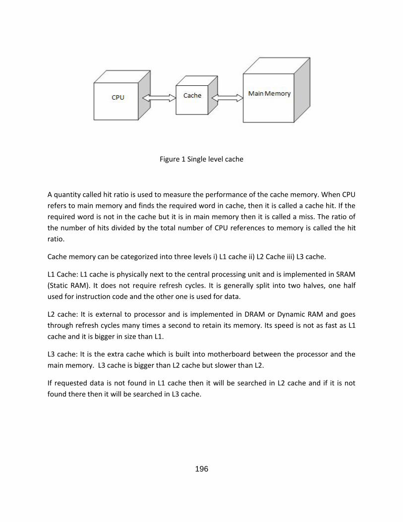
196
Figure 1 Single level cache
A quantity called hit ratio is used to measure the performance of the cache memory. When CPUrefers to main memory and finds the required word in cache, then it is called a cache hit. If therequired word is not in the cache but it is in main memory then it is called a miss. The ratio ofthe number of hits divided by the total number of CPU references to memory is called the hitratio.
Cache memory can be categorized into three levels i) L1 cache ii) L2 Cache iii) L3 cache.
L1 Cache: L1 cache is physically next to the central processing unit and is implemented in SRAM(Static RAM). It does not require refresh cycles. It is generally split into two halves, one halfused for instruction code and the other one is used for data.
L2 cache: It is external to processor and is implemented in DRAM or Dynamic RAM and goesthrough refresh cycles many times a second to retain its memory. Its speed is not as fast as L1cache and it is bigger in size than L1.
L3 cache: It is the extra cache which is built into motherboard between the processor and themain memory. L3 cache is bigger than L2 cache but slower than L2.
If requested data is not found in L1 cache then it will be searched in L2 cache and if it is notfound there then it will be searched in L3 cache.
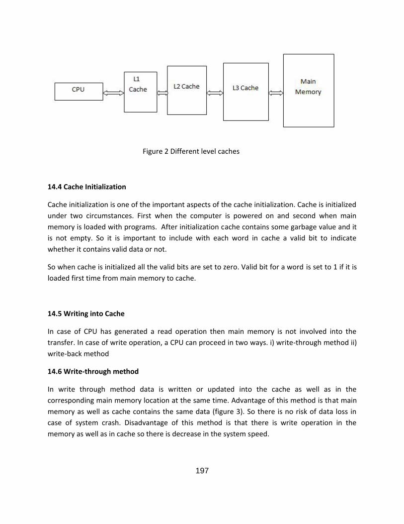
197
Figure 2 Different level caches
14.4 Cache Initialization
Cache initialization is one of the important aspects of the cache initialization. Cache is initializedunder two circumstances. First when the computer is powered on and second when mainmemory is loaded with programs. After initialization cache contains some garbage value and itis not empty. So it is important to include with each word in cache a valid bit to indicatewhether it contains valid data or not.
So when cache is initialized all the valid bits are set to zero. Valid bit for a word is set to 1 if it isloaded first time from main memory to cache.
14.5 Writing into Cache
In case of CPU has generated a read operation then main memory is not involved into thetransfer. In case of write operation, a CPU can proceed in two ways. i) write-through method ii)write-back method
14.6 Write-through method
In write through method data is written or updated into the cache as well as in thecorresponding main memory location at the same time. Advantage of this method is that mainmemory as well as cache contains the same data (figure 3). So there is no risk of data loss incase of system crash. Disadvantage of this method is that there is write operation in thememory as well as in cache so there is decrease in the system speed.
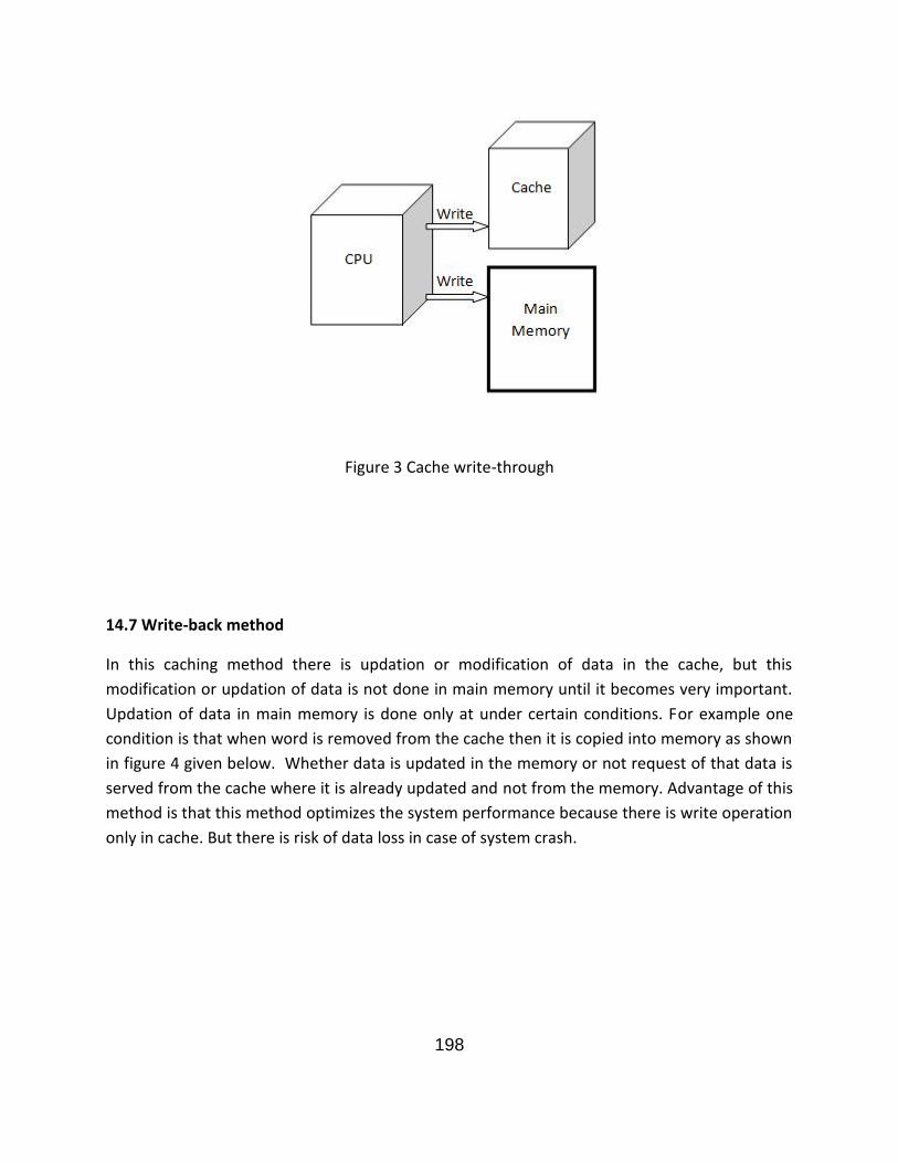
198
Figure 3 Cache write-through
14.7 Write-back method
In this caching method there is updation or modification of data in the cache, but thismodification or updation of data is not done in main memory until it becomes very important.Updation of data in main memory is done only at under certain conditions. For example onecondition is that when word is removed from the cache then it is copied into memory as shownin figure 4 given below. Whether data is updated in the memory or not request of that data isserved from the cache where it is already updated and not from the memory. Advantage of thismethod is that this method optimizes the system performance because there is write operationonly in cache. But there is risk of data loss in case of system crash.
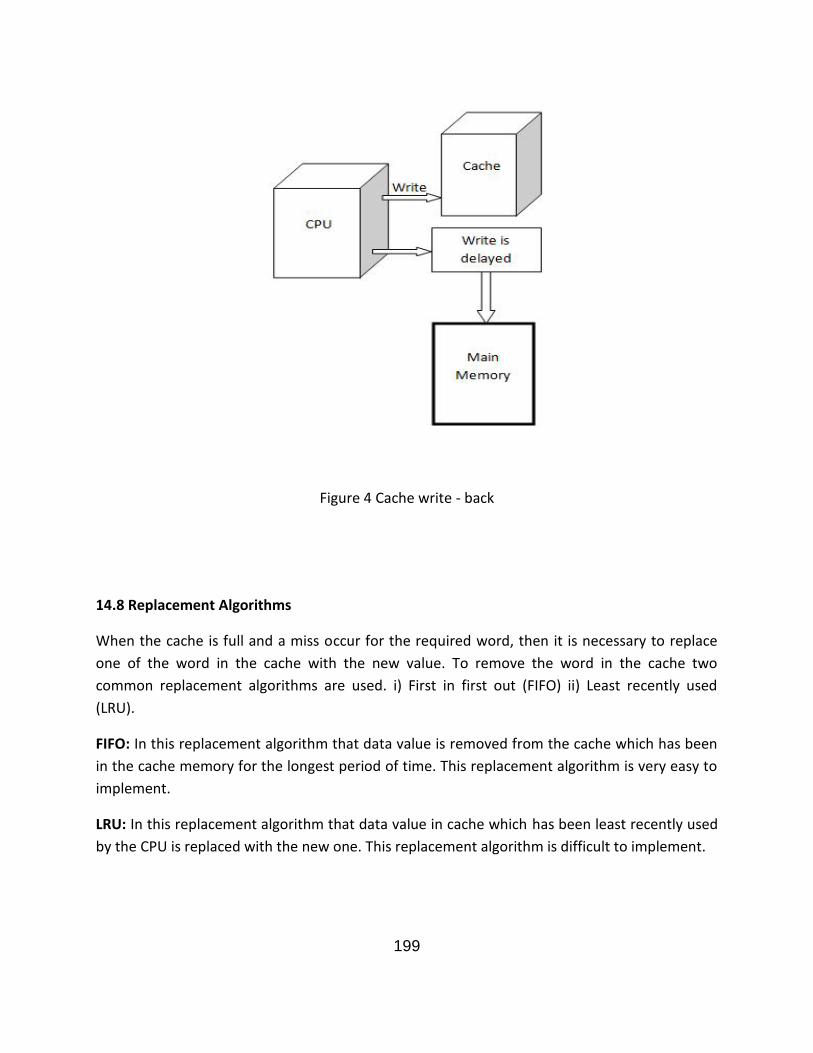
199
Figure 4 Cache write - back
14.8 Replacement Algorithms
When the cache is full and a miss occur for the required word, then it is necessary to replaceone of the word in the cache with the new value. To remove the word in the cache twocommon replacement algorithms are used. i) First in first out (FIFO) ii) Least recently used(LRU).
FIFO: In this replacement algorithm that data value is removed from the cache which has beenin the cache memory for the longest period of time. This replacement algorithm is very easy toimplement.
LRU: In this replacement algorithm that data value in cache which has been least recently usedby the CPU is replaced with the new one. This replacement algorithm is difficult to implement.
200
14.9 Summary
To compensate speed differences between the CPU and main memory one or moreintermediate memories called caches are used. Generally three levels of caches are used inmodern system depending upon their size. When the CPU refers to an address and it is found inthe cache then it is called cache hit. Due to the locality of reference property hit ratio of 0.9 andhigher have been reported. So cache memory enhances the performance of computer system.
14.10 Glossary
Cache Hit: when a word is found in cache it is called cache hit.
Hit Ratio: It is used to measure the performance of cache memory.
Locality of Reference: It is the property of programs in which references to memory at any giveinterval of time are constrained to a few localized area of memory.
14.11 Model Questions
Q.1. Write down the working of cache memory?
Q.2. What are the different levels of cache memory?
Q.3. What is cache initialization?
Q.4. Explain write-through and write-back methods.
Q.5. Discuss replacement algorithms used by cache memory.
14.12 References/Bibliography
1. Mano, M.M., Computer System Architecture, 3rd ed., PHI..2. Mano, M.M: Digital Logic and Computer Design, Prentice Hall of India.3. Stalling, W, Computer Organization and Architecture, 8th ed., PHI.4. Hayes: Computer Architecture and Organization, McGraw-Hill International Edition.5. Tanenbaum, A.S., Structured Computer Organization 5th ed., Prentice Hall of India
201
Lesson 15
Cache Memory Mapping Techniques
Structure
15.0 Objectives
15.1 Introduction
15.2 Mapping
15.3 Associative Mapping
15.4 Direct Mapping
15.5 Set Associative Mapping
15.6 Summary
15.7 Glossary
15.8 References/Bibliography/Suggested Readings
15.9 Terminal and Model Questions
15.0 Objectives
After reading this chapter students will be able to understand
Cache memory mapping Associative Mapping Direct mapping Set associative Mapping
15.1 Introduction
Cache memory is a high speed memory and small in size. Cache memory is much expansive ascompared to main memory. The basic feature of the cache memory is that it has fast accesstime. Cache mapping is the method by which the contents of main memory are transformedinto the cache memory and referenced by the CPU. These methods also affect the performanceof the computer system.
15.2 Mapping
Main features of Cache memory are that it is very small in size and has very fast access time.When a memory request is generated by CPU, then this word should be searched very fast inthe cache memory. The method/technique used to transfer the data from main memory to
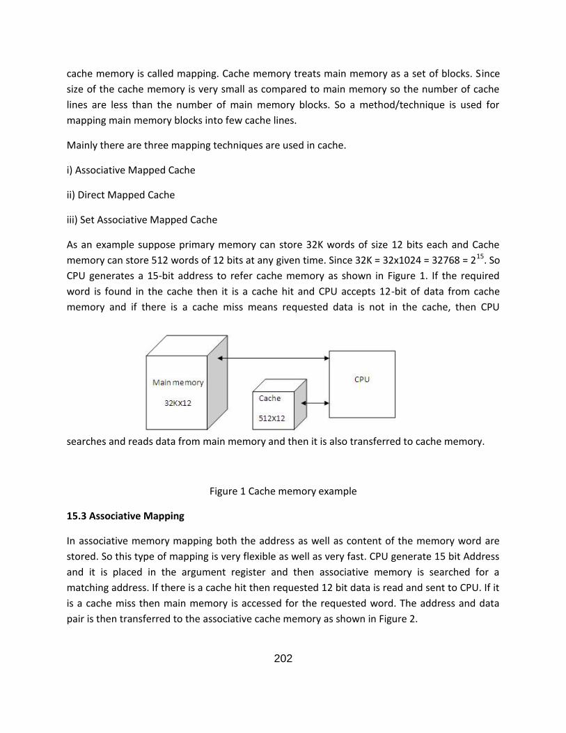
202
cache memory is called mapping. Cache memory treats main memory as a set of blocks. Sincesize of the cache memory is very small as compared to main memory so the number of cachelines are less than the number of main memory blocks. So a method/technique is used formapping main memory blocks into few cache lines.
Mainly there are three mapping techniques are used in cache.
i) Associative Mapped Cache
ii) Direct Mapped Cache
iii) Set Associative Mapped Cache
As an example suppose primary memory can store 32K words of size 12 bits each and Cachememory can store 512 words of 12 bits at any given time. Since 32K = 32х1024 = 32768 = 215. SoCPU generates a 15-bit address to refer cache memory as shown in Figure 1. If the requiredword is found in the cache then it is a cache hit and CPU accepts 12-bit of data from cachememory and if there is a cache miss means requested data is not in the cache, then CPU
searches and reads data from main memory and then it is also transferred to cache memory.
Figure 1 Cache memory example
15.3 Associative Mapping
In associative memory mapping both the address as well as content of the memory word arestored. So this type of mapping is very flexible as well as very fast. CPU generate 15 bit Addressand it is placed in the argument register and then associative memory is searched for amatching address. If there is a cache hit then requested 12 bit data is read and sent to CPU. If itis a cache miss then main memory is accessed for the requested word. The address and datapair is then transferred to the associative cache memory as shown in Figure 2.
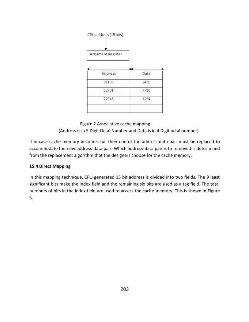
203
Figure 2 Associative cache mapping(Address is in 5 Digit Octal Number and Data is in 4 Digit octal number)
If in case cache memory becomes full then one of the address-data pair must be replaced toaccommodate the new address-data pair. Which address-data pair is to removed is determinedfrom the replacement algorithm that the designers choose for the cache memory.
15.4 Direct Mapping
In this mapping technique, CPU generated 15 bit address is divided into two fields. The 9 leastsignificant bits make the index field and the remaining six bits are used as a tag field. The totalnumbers of bits in the index field are used to access the cache memory. This is shown in Figure3.
204
Figure 3 Direct mapping example
In general if there are in suppose cache memory consists of 2k words and main memory consistof 2n words. Now n-bit memory address is divided into two fields. k-bits are used in the indexfields and n-k bits are used in the tag field. So in this example k bits for index field = 9 becausesize of cache memory is 512 х12. Size of main memory is 32Kх12. Thus, for n = 15, n-k = 6 bitsare used as tag field. Now when there is a memory request by CPU, the index field bits are usedto access the cache memory. Now the two tag values, tag field of the CPU address and tag valueread from the cache memory are compared. If these the two tag values match then it is a cachehit. If there is a cache miss then the requested word is read from the main memory. After that itis stored in the cache memory with the new tag value replacing the previous value.
An example showing direct mapping method is shown in the Figure 4 given below. The data atmain memory address zero is stored in the cache memory (index = 000, tag =00, data is=2333).So if CPU generates an address request 00000 then it is a cache hit. Now suppose requestgenerated by CPU is 02000. Now in this case index value is 000 so it is used to search cachememory. Now two tag values are compared but cache tag value is 00 and address tag value is02. So it is a cache miss and now memory is searched for the requested data and memory data5670 is transferred to the CPU. And the cache memory is also updated with a tag of 02 and data5670.
205
Figure 4 Direct mapping
15.5 Set Associative Mapping
In this type of memory organization the same index address value is used to store two or morethan two data values in the cache memory. Each data word and its tag value are stored in thecache memory. The number of tag and data items under one index value in the cache memoryis called a set. An example of a set associative cache memory mapping is given below in thefigure 5. It has a set size of two. Each index address value maps to two data words and theirassociated tag values. Since each tag consists of six bits and each data word has 12 bits so thetotal word length in this example is 6+12+6+12 = 36 bits. An index address of 9 bits can have29= 512 words. Thus the size of cache memory in this example is 512х36. It can hold 512+512 =1024 words of main memory. As shown in the Figure 5 the data stored at addresses 01000 and02000 of main memory are stored in the cache memory at index value 000. Similarly the wordsat address 02777 and 00777 are stored in cache memory at index value 777. When there is aCPU memory request, the index value of the address is used to search cache memory. The tagfield value is then compared with both the tag values in the cache memory to find whether it isa cache hit or not. The comparison logic is similar like an associative memory search. That iswhy it is called as set associative.
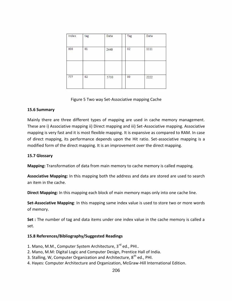
206
Figure 5 Two way Set-Associative mapping Cache
15.6 Summary
Mainly there are three different types of mapping are used in cache memory management.These are i) Associative mapping ii) Direct mapping and iii) Set-Associative mapping. Associativemapping is very fast and it is most flexible mapping. It is expansive as compared to RAM. In caseof direct mapping, its performance depends upon the Hit ratio. Set-associative mapping is amodified form of the direct mapping. It is an improvement over the direct mapping.
15.7 Glossary
Mapping: Transformation of data from main memory to cache memory is called mapping.
Associative Mapping: In this mapping both the address and data are stored are used to searchan item in the cache.
Direct Mapping: In this mapping each block of main memory maps only into one cache line.
Set-Associative Mapping: In this mapping same index value is used to store two or more wordsof memory.
Set : The number of tag and data items under one index value in the cache memory is called aset.
15.8 References/Bibliography/Suggested Readings
1. Mano, M.M., Computer System Architecture, 3rd ed., PHI..2. Mano, M.M: Digital Logic and Computer Design, Prentice Hall of India.3. Stalling, W, Computer Organization and Architecture, 8th ed., PHI.4. Hayes: Computer Architecture and Organization, McGraw-Hill International Edition.
207
5. Tanenbaum, A.S., Structured Computer Organization 5th ed., Prentice Hall of India
15.9 Terminal and Model Questions
Q.1. Which cache mapping technique is the fastest?
a) Direct mapping b) Set associative mapping c) Fully associative mapping
Q.2. What is the locality of reference principle in case of cache memory?
Q.3. Explain different mappings used in cache memory.
Q.4. What are the disadvantages of each mapping technique?
Q.5. What are three field used in set- associative cache?

208
Lesson 16
Mobile Devices Architecture
Structure
16.0 Objectives16.1 Introduction16.2 Harvard Architecture
16.2.1 Modified Harvard Architecture16.2.2 Uses of Harvard Architecture16.2.3 Advantages of Harvard Architecture16.2.4 Disadvantages of Harvard Architecture16.2.5 Harvard Architecture vs Von Neumann Architecture
16.3 Mobile Device Architecture16.3.1 Android
16.3.1.1 Features of Android16.3.1.2 Android Architecture16.3.1.3 Advantages of Android16.3.1.4 Disadvantages of Android
16.3.2 Symbian16.3.2.1 Features of Symbian16.3.2.2 Symbian Architecture16.3.2.3 Advantages of Symbian16.3.2.4 Disadvantages of Symbian
16.3.3 Windows Lite16.3.3.1 Features of Windows Lite16.3.3.2 Windows Architecture
16.4 Layered Approach Architecture16.4.1 Mobile Device Architectural Layers- An Example16.4.2 Open Source Interconnection Layers- An Example
16.5 Summary16.6 Glossary16.7 Answers to Check Your Progress/Suggested Answers to SAQ16.8 Terminal and Model Questions
209
16.0 Objectives
The main objective of this chapter is to make students understand:
What is Harvard architecture? Various mobile device architectures Most popular mobile OS- Android Symbian OS and Windows Lite OS for mobile devices What is Layered approach architecture
16.1 Introduction
This chapter aims at thriving the knowledge of the readers by giving information on variousarchitectures of computer and the mobile devices. The chapter will commence by introducingthe Harvard architecture that is mostly used in today’s modern time. Then various mobiledevice architectures will be explained in which Android OS, Symbian OS and Windows Lite willbe explained in detail. There features, architecture, advantages and disadvantages will bestudied in brief. Lastly, the layered approach of the architectures will be studied with examples.
16.2 Harvard Architecture
The simple computer architecture is based on the two common architectural schemes- Harvardarchitecture and Von Neumann architecture. Both these architectural schemes provide aseparate view to design the computer.
Figure 16.1: Block diagrams of Harvard Architecture and Von Neumann Architecture
The Harvard architecture is a simple computer architecture that contains separate instructionand data memory. The instructions and data are stored in different physical storage. They donot share the same memory space. While in von Neumann architectural scheme, instructionsand data share same memory storage. The Harvard architecture comprises two separate buses-
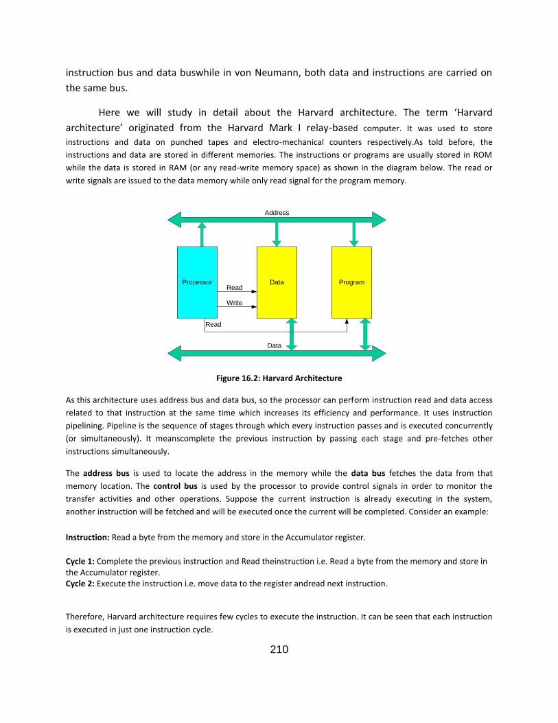
210
instruction bus and data buswhile in von Neumann, both data and instructions are carried onthe same bus.
Here we will study in detail about the Harvard architecture. The term ‘Harvardarchitecture’ originated from the Harvard Mark I relay-based computer. It was used to storeinstructions and data on punched tapes and electro-mechanical counters respectively.As told before, theinstructions and data are stored in different memories. The instructions or programs are usually stored in ROMwhile the data is stored in RAM (or any read-write memory space) as shown in the diagram below. The read orwrite signals are issued to the data memory while only read signal for the program memory.
Figure 16.2: Harvard Architecture
As this architecture uses address bus and data bus, so the processor can perform instruction read and data accessrelated to that instruction at the same time which increases its efficiency and performance. It uses instructionpipelining. Pipeline is the sequence of stages through which every instruction passes and is executed concurrently(or simultaneously). It meanscomplete the previous instruction by passing each stage and pre-fetches otherinstructions simultaneously.
The address bus is used to locate the address in the memory while the data bus fetches the data from thatmemory location. The control bus is used by the processor to provide control signals in order to monitor thetransfer activities and other operations. Suppose the current instruction is already executing in the system,another instruction will be fetched and will be executed once the current will be completed. Consider an example:
Instruction: Read a byte from the memory and store in the Accumulator register.
Cycle 1: Complete the previous instruction and Read theinstruction i.e. Read a byte from the memory and store inthe Accumulator register.Cycle 2: Execute the instruction i.e. move data to the register andread next instruction.
Therefore, Harvard architecture requires few cycles to execute the instruction. It can be seen that each instructionis executed in just one instruction cycle.
ProgramData
Address
Data
ProcessorRead
Write
Read
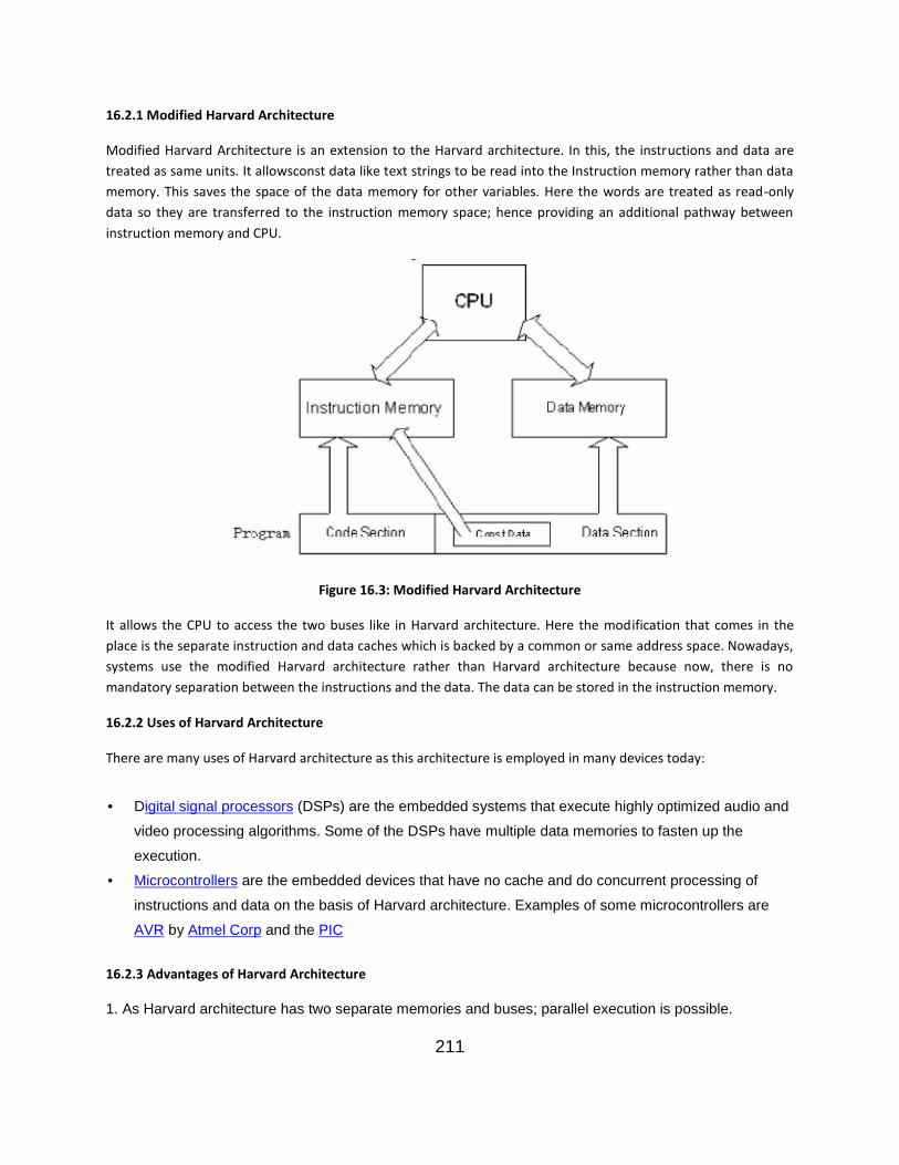
211
16.2.1 Modified Harvard Architecture
Modified Harvard Architecture is an extension to the Harvard architecture. In this, the instructions and data aretreated as same units. It allowsconst data like text strings to be read into the Instruction memory rather than datamemory. This saves the space of the data memory for other variables. Here the words are treated as read-onlydata so they are transferred to the instruction memory space; hence providing an additional pathway betweeninstruction memory and CPU.
Figure 16.3: Modified Harvard Architecture
It allows the CPU to access the two buses like in Harvard architecture. Here the modification that comes in theplace is the separate instruction and data caches which is backed by a common or same address space. Nowadays,systems use the modified Harvard architecture rather than Harvard architecture because now, there is nomandatory separation between the instructions and the data. The data can be stored in the instruction memory.
16.2.2 Uses of Harvard Architecture
There are many uses of Harvard architecture as this architecture is employed in many devices today:
Digital signal processors (DSPs) are the embedded systems that execute highly optimized audio andvideo processing algorithms. Some of the DSPs have multiple data memories to fasten up theexecution.
Microcontrollers are the embedded devices that have no cache and do concurrent processing ofinstructions and data on the basis of Harvard architecture. Examples of some microcontrollers areAVR by Atmel Corp and the PIC
16.2.3 Advantages of Harvard Architecture
1. As Harvard architecture has two separate memories and buses; parallel execution is possible.
212
2. It needs fewer instruction cycles to execute the instructions; thus increasing the speed of the CPU.3. It contains pipeline stages that increase the efficiency and speed of the execution of the instructions.4. Instruction and data memory can use varied cell sizes.
16.2.4 Disadvantages of Harvard Architecture
1. If data memory is free, it cannot be used by other instructions as it can only store the data.2. This architecture is expensive as it needs two memory blocks and two buses.3. As the instruction memory is read-only, program contents cannot be modified by itself.4. Designing of control unit for two different buses is complex.
16.2.5 Harvard Architecturevs Von Neumann Architecture
Harvard Architecture Von Neumann Architecture1. The basic difference is that the Harvardarchitecture has two separate memories for data andinstructions.
1. The Von Neumann architecture has single memorystorage for both the data and the instructions.
2. It needs only one instruction cycle to complete aninstruction.
2. It uses two instruction cycles to complete oneinstruction.
3. Programs are stored in ROM so they cannot bemodified by themselves.
3. Programs share the same memory which can beread-write so they can modify themselves.
4. It is more expensive. 4. It is less expensive than Harvard architecture.5. It contains two separate buses. 5. It contains only one bus.6. Harvard Architecture is complex to build. 6. Von Neumann is less complex than Harvard.7. If the data memory is available for use and is free;it cannot be used for storing instructions.
7. Shared memory has no such problem.
16.3 Mobile Devices Architecture
Mobile devices are the handheld devices that are used to communicate with other people. Mobiles have becomethe basic need of every human being. People living in one part of world can interact with the person living in anyother part of the world. Earlier, mobiles were used only for telephony services and messaging but now there use isbeyond simple phone calling. Now mobiles are used to access internet, to make documents, to do socialnetworking etc. There use is unlimited. The cell phones are now screen touch. In a single touch, you can transfermoney from your account to another on mobiles. All the e-commerce transactions are now in your hand viamobiles.
Check Your Progress
Q1. What is the basic difference between Harvard and Von Neumann architecture?
Q2. bus carries the data from the memory.
213
These mobile devices are designed according to the user needs. The operating system on which thedevice has been built is the central feature. The operating system does all the changes. The keypad to touch screenphone is the boon given by the operating system.Some points need to be understood for developing thearchitecture:
Operating system is the system software which is used to provide an interface between the user andthe device. Operating system makes this interaction easier and the user need not go into the detailsabout the implementation of the device. It synchronizes various tasks, provide memory management andpower management. It contains libraries that contain the definitions and implementation details of thesoftware and the hardware. For example, Android OS, Symbian OS etc. Programming Languages are the computer languages. They are used to write the operating system.These languages can be C, C++, Java, Visual basic etc. Middleware is the software component which is used to link the applications with the networkcomponents. For example, Bluetooth, Hot spot etc. Protocols are the set of rules that govern the communication. There are various communicationprotocols in mobile devices like GSM900, Zigbee, WLAN etc. Layers are needed that are used to provide separation between the various components.
16.3.1 Android
With the gigantic increase in the production of the mobile devices, its reliability, connectivity, performance andavailability has become chief concern. To handle these kinds of issues, a smart and faster solution has been builtfor the mobile devices known as Android. Android is a very familiar term nowadays. It is an open source themobile operating system which was developed by Android Inc. Later in 2005, Google purchased android. It is aLinux-based operating system. Google with the Open Handset Alliance (OHA), then further collaborated topromote android. OHA is a conglomerate of 84 companies that shake hands to develop the open standards for themobile devices. Android is now being governed and maintained by Android Open Source Project (AOSP).
Figure 16.4: Android Logo
Android is an operating system which acts as middleware and is a platform for key applications. Androids are usedto develop the applications easily and conveniently. It is used as an OS in mobile devices, tablets, digital cameras,TVs, some wearable devices (like android wrist watch) etc. There are many releases of androids like Cupcake,Donut, Ice-cream sandwich, Jellybean, KitKat, and Lollipop. The current android version released is Marshmallow.More than 1 million android devices get activated every day round the world.
16.3.1.1 Features of Android
214
Android is a prevailing operating system that has many features to offer:
1. User Interface- Android provides us a user-friendly interface with beautiful icons that one can see onthe mobile devices. Icons and widgets provide an easy way to use the devices.2. Connectivity- We can connect to the internet or to any other device through any medium; like Wi-Fi orBluetooth.3. Multi-tasking- One can do multi-tasking on the devices i.e. you can jump to any other task while othertasks may be running in parallel. It can open multiple windows on the screen simultaneously.4. Multi-touch- Android provides the feature of multi-touch which is the basic feature in mobiles ortablets.5. Multi-lingual- Android supports multi-language facility. We can use any language while texting orbrowsing on the net.6. Manage Memory- Android operating system is designed to manage the memory requirements. Itmanages the RAM in order to reduce the memory space and the power consumption by the devices.7. Resizable Widgets- Widgets can be resized to save the space and also can be expanded to showmore and more contents.8. Applications- Android provides many applications which extend the functionality of the devices. Appscan be installed on the mobile or the tablet from various application stores like Google play store, Amazonapp store, Slide, F-Droid etc.
16.3.1.2 Android Architecture
The Android architecture is a layered architecture which has four layers- Applications, Application Framework,Libraries and Android Runtime and Linux Kernel. Android incorporates a powerful architecture in which everylayer has some specific and important task to do and provide services to the other layers above it. It isimplemented as software heap or stack. We will study every layer of the architecture in detail.
Figure 16.5: Layered Architecture of Android
215
(a) Linux Kernel
Linux Kernel is the basic layer of the android architecture. The whole architecture is built upon this layer.It provides an abstraction between the android hardware and the other layers of the architecture i.e. it isthe Linux kernel that communicates with the hardware. It contains various important device drivers likecamera driver, display driver, audio driver, USB driver, flash memory driver (flash memory is non-volatileelectronically erasable memory) etc. Drivers are the software that manages communication with thehardware and other devices. For example, this layer includes Bluetooth driver. As every android devicehas Bluetooth hardware so this driver is used to communicate with other Bluetooth hardware. Linuxkernel also handles the memory management, power management and other network relatedfunctionalities. It has a Binder (IPC) driver which provides inter-process communication and provides highperformance.
Linux kernel is being selected for the android base layer because it is great in memory andprocess management and is a secure model. Hence android is based on the Linux kernel which takes outthe pain of how to provide interface or communicate with the other devices.
(b) Libraries
It is the next layer above the Linux kernel. Libraries are the resources that are used by the programs todevelop the software. It is the collection of implementation details which are written in programminglanguage and contains documentation, configuration details etc. These libraries are written in C and C++languages. Some of the native libraries are:
Surface Manager- It composes different drawings or windows on the screen of different applications. Itcontains off-screen buffer in which application’s windows get stored first rather be directly displayed onthe screen. It combines with other drawings from the off-screen buffer and forms a complete windowwhich is displayed on the screen.
Media Framework- This library contains the media codes that are used for playing and recordingaudio/video in different media formats like MP3, MP4, MPEG4 etc.
SQLite- It is a relational database engine used for the data storage in android.
OpenGL | ES- It is 3D graphic engine which renders the 3D content on the screen.
FreeType- This library is used to generate fonts in android.
WebKit- It is a browser engine that supports CSS, Javascript, HTML content.
SGL (Scalable Graphics Library)-It is 2D graphic engine which renders 2D content on the screen.
SSL (Secure Socket Layer)- It provides enhanced security to the android
Libc-Libc is a standard C library. It is small in size and is called Bionic library. It is used to optimize thememory of the processes or threads and also reduces the initiate time of the new threads. It providessupport for the android services.
(c) Android Runtime
It is a section in parallel to the libraries section of the second last layer. It contains the two importantfeatures- Dalvik Virtual Machine and Core Java Libraries.
216
Dalvik Virtual MachineAndroid devices encompass its own Virtual Machine (VM) known as Dalvik Virtual Machine (DVM). It isjust like Java Virtual Machine. A virtual machine is a kind of machine which is installed on the computerthat acts as a specialized hardware. For example, we can install virtual machine to run Windows NT on aPC running which is already Windows 7. It works as a hypothetical computer. The DVM is used to runvarious android apps and works efficiently in case of less memory requirements and low battery capacity.It is best suitable in embedded system environments. DVM uses its own byte codes and executes.dexfiles (Dalvik executable file). DVM converts .class files of Java to .dex files during run time. DVM isbased on Just In Time compiler of Java, in which part of the code to be executed is compiled and rest ofthe code is compiled and cached as you progress further in app. DVM allows multiple virtual machines tobe executed on a single device in various processes which provides memory management, security etc.
In KitKat version, Android Run Time (ART) was introduced instead of DVM. It pre-compilesthe whole code which is called Ahead of Time compilation (AOT), thus eliminating the need to compileand cache the code in later stages. It sufficiently increases the speed of the processes, uses less CPUand has improved garbage collection.
Core Library
Core libraries are the Java libraries which provide a powerful and efficient development platform. Itcontains all the central class libraries, utilities, file and network access, graphics and input-output libraries.
(d) Application Framework
Application framework is the next layer which acts as the building block for the application. It is this layerthat interacts directly with the applications. This layer is known to maintain the functions of the device liketelephone services, resource management etc. It provides the Application Program Interface (API). Someof the units included in this layer are discussed below:
Activity Manager- It is used to manage the application life cycle. Content Provider- It is used by the applications to share data among them and also provide dataaccess within the applications. Resource Manager- It provides access to non-code android resources like graphics, color settings,strings etc. Notifications Manager- Notification Manager is used to display alerts and various other notifications tothe user. Telephony Manager- As the name suggests, it helps to manage and maintain the voice calls inapplications. Location Manager- It is used to manage the location via GPS or cell stations. View Manager- View manager manages the views which are collaborated to form user interfaces. Window Manager- It manages various windows that are to be displayed on the screen and alsoperform window rotations and transitions. Package Manager- Package manager is used as an interface to install packages in the android andalso to manipulate and upgrade the installed packages.
(e) Applications

217
Applications is the top most layer in the android architecture. It is this layer through which user interacts. Itconsists of many applications are pre-built in the android devices like:
1. Browser App2. Contacts App3. Home4. Messaging App5. Dialer App
User can also write its own application into this area. For example, we download our own apps from theGoogle play store like AppLocker etc. All these user downloaded apps are stored in this layer. Also, theapplications that user download will replace any existing application. Every application runs in its ownmemory space and within its own Dalvik Virtual Machine. We can install as many applications as we wantbut within memory space.
Hence android provides us seamless benefits of using the mobile devices or the tablets. Itsfeatures are endless and are growing day-by-day. Its customizable nature makes its use ever expanding.Android’s benefits and luring features will soon result it into an operating system that will be used inlaptops and desktops.
16.3.1.3 Advantages of Android
1. We can run as many applications as we want simultaneously. We can do multi-tasking and open manywindow screens in parallel.2. Access to thousands of applications from play store which a user can install on its android device andcan have its benefits.3. Notifications are broadcasted through alerts or messages. In some devices. LED light blinks thatnotifies you that you have missed a call.4. Widgets help you to open many settings and expand or shrink the same.5. Browsers, GPS, games, social networking websites; all can be accessed on a single device in fractionof seconds.
16.3.1.4 Disadvantages of Android
1. Advertisements are one of the disadvantages of using android phones. Ads are displayed on thescreen that may cause third-party to intrude our device.2. Memory storage is also a problem in some android devices. We are limited to install apps according tothe memory size.3. No doubt, the developers tried to fix the battery consumption but still it is an issue. Android causesmany processes to run at the background that not only use RAM but also battery power.
Check Your Progress
Q3. What are the various libraries that are used in android?
Q4. What is DVM?
Q5. In which files does the DVM converts the class files of Java?
218
16.3.2 Symbian
Before going into the details about the Symbian architecture, let us have a look how it came intoexistence. Before Symbian, a mobile giant company Psion designed an operating system called EPOCwhich was graphical operating system and was mainly developed for the portable devices like mobiles.But because of the technical advancements, the EPOC was changed into Symbian OS which was acombined venture of Symbian Ltd. (i.e. Psion) and other companies like Nokia, Samsung, Motorola andSony Ericsson.
Symbian is a closed-source operating system (initially open-source) based on C++ that wasdeveloped to run on Acorn RISC Machine (ARM) processor. First Symbian based phone was released byEricsson ER380. It supported other Symbian-based platforms like S60, User Interface Quartz (UIQ) andMOAP.
Figure 16.6: Symbian OS logo
16.3.2.1 Features of Symbian
1. User Interface- Symbian OS provides a graphical user interface. Various user interface is supportedby Symbian like S60, UIQ.2. Multi-lingual- This OS supports multiple languages that can be used on device. The current release ofSymbian named Symbian Belle supported 48 languages.3. Browser- Symbian uses WebKitliabrary for browsers which help to show the HTML, CSS andJavascript content.
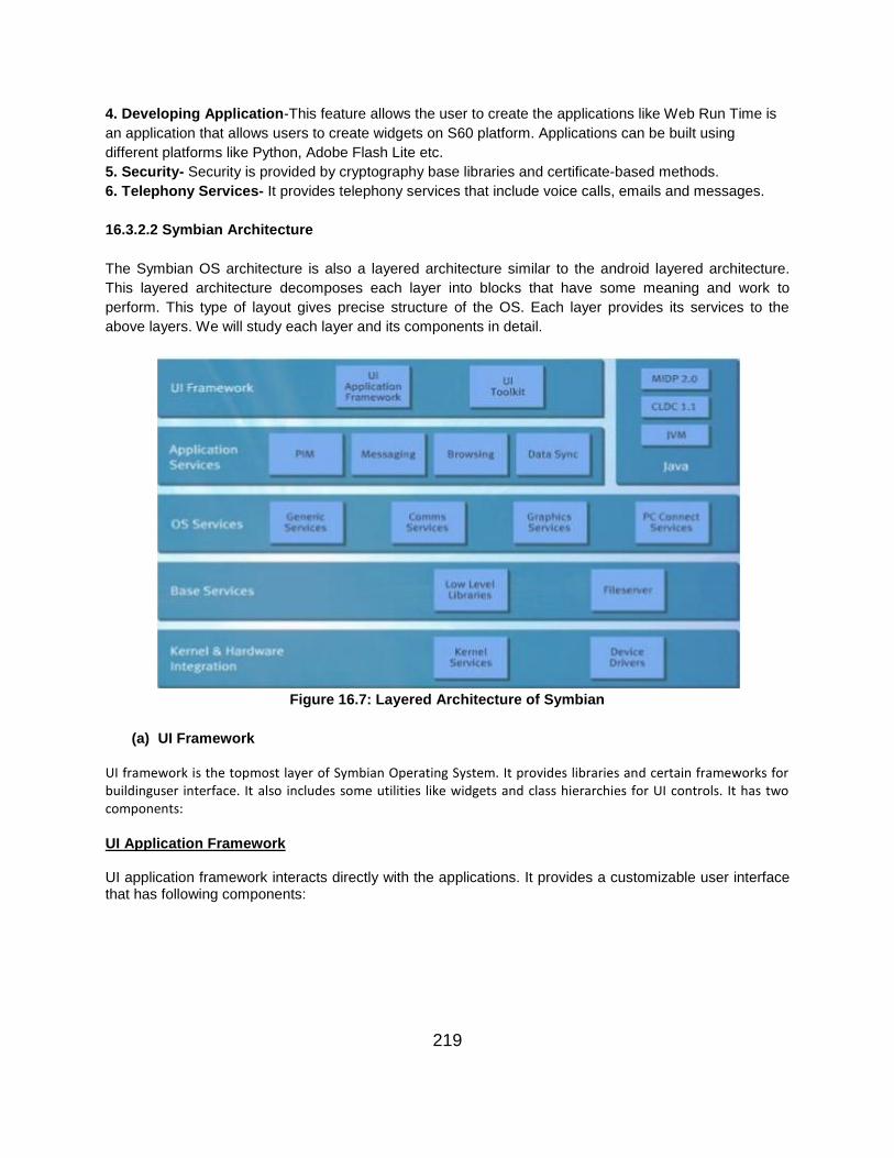
219
4. Developing Application-This feature allows the user to create the applications like Web Run Time isan application that allows users to create widgets on S60 platform. Applications can be built usingdifferent platforms like Python, Adobe Flash Lite etc.5. Security- Security is provided by cryptography base libraries and certificate-based methods.6. Telephony Services- It provides telephony services that include voice calls, emails and messages.
16.3.2.2 Symbian Architecture
The Symbian OS architecture is also a layered architecture similar to the android layered architecture.This layered architecture decomposes each layer into blocks that have some meaning and work toperform. This type of layout gives precise structure of the OS. Each layer provides its services to theabove layers. We will study each layer and its components in detail.
Figure 16.7: Layered Architecture of Symbian
(a) UI Framework
UI framework is the topmost layer of Symbian Operating System. It provides libraries and certain frameworks forbuildinguser interface. It also includes some utilities like widgets and class hierarchies for UI controls. It has twocomponents:
UI Application Framework
UI application framework interacts directly with the applications. It provides a customizable user interfacethat has following components:
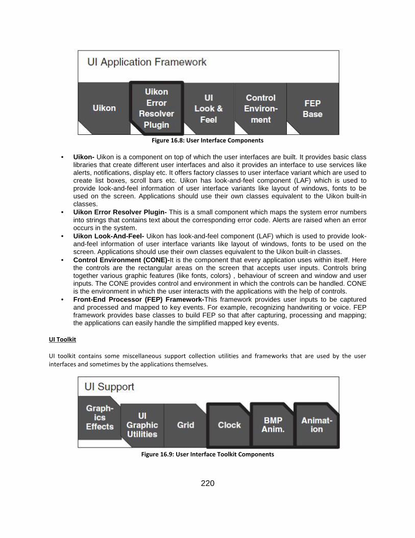
220
Figure 16.8: User Interface Components
Uikon- Uikon is a component on top of which the user interfaces are built. It provides basic classlibraries that create different user interfaces and also it provides an interface to use services likealerts, notifications, display etc. It offers factory classes to user interface variant which are used tocreate list boxes, scroll bars etc. Uikon has look-and-feel component (LAF) which is used toprovide look-and-feel information of user interface variants like layout of windows, fonts to beused on the screen. Applications should use their own classes equivalent to the Uikon built-inclasses.
Uikon Error Resolver Plugin- This is a small component which maps the system error numbersinto strings that contains text about the corresponding error code. Alerts are raised when an erroroccurs in the system.
Uikon Look-And-Feel- Uikon has look-and-feel component (LAF) which is used to provide look-and-feel information of user interface variants like layout of windows, fonts to be used on thescreen. Applications should use their own classes equivalent to the Uikon built-in classes.
Control Environment (CONE)-It is the component that every application uses within itself. Herethe controls are the rectangular areas on the screen that accepts user inputs. Controls bringtogether various graphic features (like fonts, colors) , behaviour of screen and window and userinputs. The CONE provides control and environment in which the controls can be handled. CONEis the environment in which the user interacts with the applications with the help of controls.
Front-End Processor (FEP) Framework-This framework provides user inputs to be capturedand processed and mapped to key events. For example, recognizing handwriting or voice. FEPframework provides base classes to build FEP so that after capturing, processing and mapping;the applications can easily handle the simplified mapped key events.
UI Toolkit
UI toolkit contains some miscellaneous support collection utilities and frameworks that are used by the userinterfaces and sometimes by the applications themselves.
Figure 16.9: User Interface Toolkit Components

221
Graphics Effects- As the name suggests, it provides graphical effects like rotating or resizingwindows. It also provides flicker-free animation effects on the windows.
UI Graphic Utilities- It provides utilities to the user interface like font, color, text, numberconversion features. It helps to perform mapping from logical to physical colors, manipulatingfonts etc.
Grid- Grid is a component that provides print preview of the excel sheets and presentations. Clock- Clock is used to provide timing to the animations. BMP Animation- It offers bitmap based animations. Animation-Animation component is used to give animation effects to the window screen like fade
effects, swing effects etc.
(b) Application Services
Application services is the second layer in the Symbian OS architecture. This layer includes serviceswhich are used by the application engines directly or indirectly. It provides general services, systemservices and application specific services. It offers support for internet connectivity, web browsers andother communication protocols like TELNET. PIM application includes application related to phone likephonebook, alarms and calendar. It contains printer server that offers support for printing documents.
Messaging service was included even in the first release of Symbian OS. It providesmessaging service like emails, texts, MMS. Data Sync services provide synchronization among the dataof applications.
(c) Operating System Services
OS services layer is the third layer in the Symbian OS architecture that provides libraries and framework for theoperating system. This layer contains the higher-level system services. These services give support to other systemcomponents, applications and also provide support tohigher layers. For example, graphics services,connectivityservices and communication services likenetworking, telephony. These services are given below in detail:
Generic Services
These services are used directly by the applications, system and some libraries. These services include: Logging and task-scheduling services The C Standard Library used by system components and is also used when user want to port the
software. Libraries supporting certificate-based and cryptographic security.
Comms Services
Comms means communication. These services include the communication services i.e. art of transferring andmoving data between different device over the network. It includes telephony services that support 2G or 3Gnetworks, GSM or CDMA mobile phones. It also supports GPRS and EDGE data packets. For networking, it supportsWi-Fi (appeared in Symbian OS 9 release), FTP, HTTP etc.
Multimedia and Graphics Services
The multimedia and graphics services provide graphical services to the operating system. The various serviceswhich are included in this block are:

222
Figure 16.10: Multimedia Servives
It provides support for 2D bitmap graphics and 3D bitmap graphics, alert handling, fontmanipulation, windowing and some low-level support for printing.
Multimedia services include camera, tuner, recording, sound and video capturing, API for stillimages, playing audio and video.
Connectivity Services
These services include device-side connectivity support like backup and restore, browsing, file transfer andapplication installation. In this, device to host services can be created which will be based on TCP/IP suite.
(d) Base Services
Base services is the fourth layer of the layered architecture of the Symbian OS. This layer contains user-sideservers, libraries, utilities and framework that are constructed on the kernel layer in order to provide services tothe upper Operating system layer. It contains various servers and libraries which are discussed below:
User Library and File Server
The User Library and the File Server provide an interface to the kernel by implementing client-server model. Theyrun on the user-side thus protecting the kernel from the programming errors and the time latencies.
The File Server manages file accesses by the clients. It does this through client-side file-serversessions. The file server framework contains plug-ins for the implementation of file systems. Thisserver listens to the client requests and passes them to the file system. It has an embedded ReadOnly Memory (ROM) file system.
The User Library provides very essential functionalities to the applications which include datatypes, active objects, clean up and some low-level services
Low Level Libraries

223
The low level libraries contain certain framework and libraries which are useful for the system and theapplications. This includes plug-ins, system utilities, cryptography base library, Zip compression base library etc. Italso contains management techniques for power and shut down of the system.
(e) Kernel and Hardware Integration
The kernel and hardware integration is the base layer in the Symbian OS architecture on which the all layers arebuilt on. It is used to boot and run the kernel. It also does the task of scheduling the OS kernel, manage memoryresources and handles interrupts. It implements thread process model in order to create, manage and schedulevarious threads. It also implements power model that manages the device power state. It also contains logicaldevice drivers (plug-ins) and physical device drivers (plug-ins to logical drivers) like Audio/Video drivers, USB driver,Ethernet Driver etc.
(f) Java Block
Java is an important platform in mobile phones for developing various games, media and utilities. TheSymbian OS is based on Java Micro Edition (ME). Java consists of Java Virtual Machine (JVM) to runjava applications on the device. It consist of configuration type- Connected Limited Device Configuration(CLDC) and some profile utilities Mobile Information Device Profile (MIDP).
16.3.2.3 Advantages of Symbian
1. Its connectivity is easier and faster.2. It does resource utilization in better way.3. Symbian OS is small but it carries lot of features in it.4. Easy to use Symbian based devices. Manages memory requirements well.5. As it is based on C++, it is easy and convenient to configure and change the OS according to the need.
16.3.2.4 Disadvantages of Symbian
1. Symbian OS is susceptible to viruses.2. It is not suitable for PCs or any wearable devices.3. Symbian OS was not up to the mark and could not met the market requirements with time.
Check Your ProgressQ7. What is Uikon?
Q8. What are the components in UI Toolkit?
Q9. Which of the following services provide telephony services?a. Connectivity Servicesb. Comms Services

224
16.3.3 Windows Lite
The third operating system for mobile devices is the Windows OS. It is developed by the renownedMicrosoft Corporation. It is written in C++ language and is popular among the mobiles of Nokia. Microsofttook over Nokia and placed its OS in the Nokia phones which nowadays are called Window Phones.Windows 10 is the new version released by the Microsoft in January 2015.
Figure 16.11: Windows 10 logo16.3.3.1 Features of Windows Lite
1. User Interface- Windows provide beautiful user interface. The home screen consists of Live Tiles that are theicons which links to the applications, functions and features. These tiles are resizable and movable.2. Multi-touch- Windows like other OS uses multi-touch. It provides touch screen phones.3. Web Browser- Internet Explorer, the web browser by the windows is the pre-installed browser in the phone.4. Multi-media- Windows provide Xbox music nowadays to play and record the multimedia. Earlier Zune softwarewas used.5. Office Suite- This is the most amazing feature in the Windows mobile that it comes with pre-installed OfficeSuite. You can manage your word, excel, presentation documents on your handheld device.6. Multi-tasking- Like any other mobile OS, it also provides multi-tasking. We can do various works simultaneously.
16.3.3.2 Architecture of Windows
The architecture of Windows is also layered. The layers separate the components from each other. Thisarchitecture is of Windows 7. There are 5 layers. These layers are just an overview of the operating system.
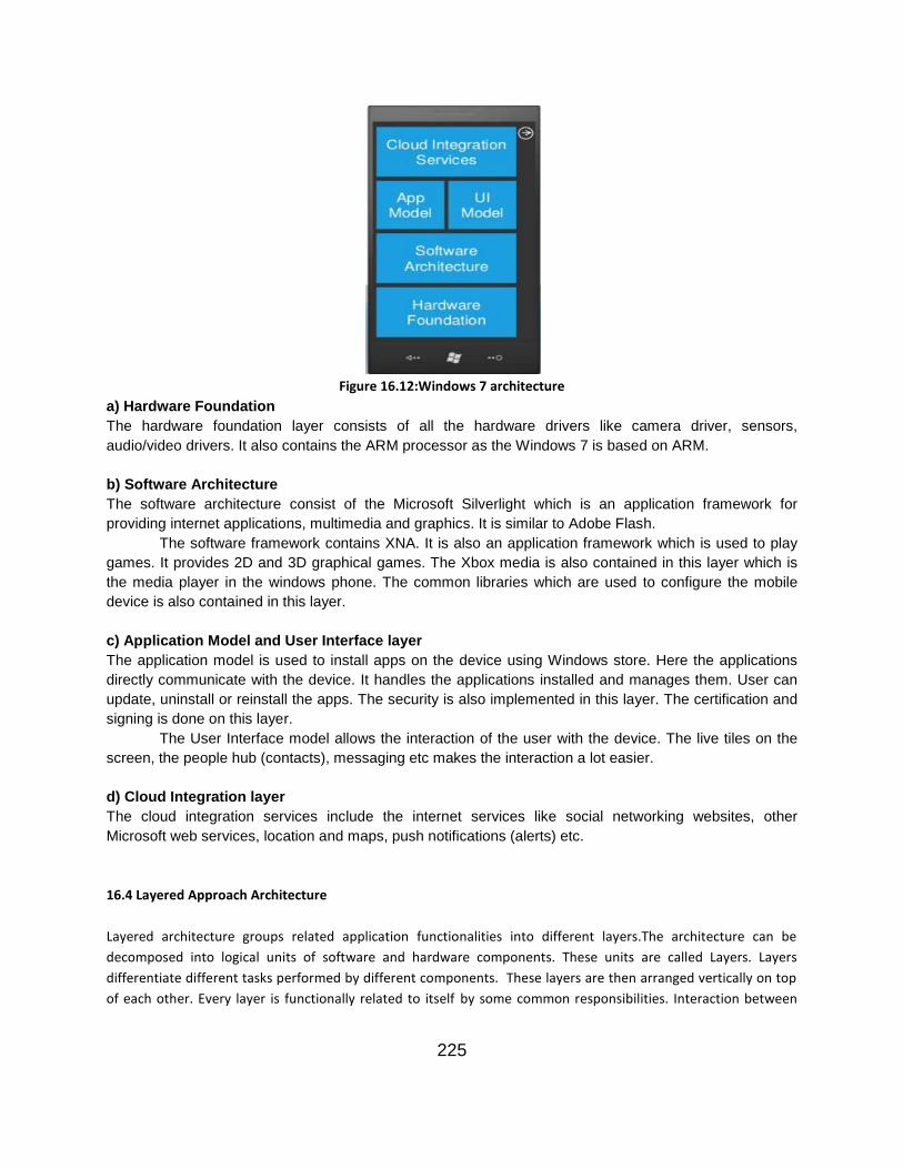
225
Figure 16.12:Windows 7 architecturea) Hardware FoundationThe hardware foundation layer consists of all the hardware drivers like camera driver, sensors,audio/video drivers. It also contains the ARM processor as the Windows 7 is based on ARM.
b) Software ArchitectureThe software architecture consist of the Microsoft Silverlight which is an application framework forproviding internet applications, multimedia and graphics. It is similar to Adobe Flash.
The software framework contains XNA. It is also an application framework which is used to playgames. It provides 2D and 3D graphical games. The Xbox media is also contained in this layer which isthe media player in the windows phone. The common libraries which are used to configure the mobiledevice is also contained in this layer.
c) Application Model and User Interface layerThe application model is used to install apps on the device using Windows store. Here the applicationsdirectly communicate with the device. It handles the applications installed and manages them. User canupdate, uninstall or reinstall the apps. The security is also implemented in this layer. The certification andsigning is done on this layer.
The User Interface model allows the interaction of the user with the device. The live tiles on thescreen, the people hub (contacts), messaging etc makes the interaction a lot easier.
d) Cloud Integration layerThe cloud integration services include the internet services like social networking websites, otherMicrosoft web services, location and maps, push notifications (alerts) etc.
16.4 Layered Approach Architecture
Layered architecture groups related application functionalities into different layers.The architecture can bedecomposed into logical units of software and hardware components. These units are called Layers. Layersdifferentiate different tasks performed by different components. These layers are then arranged vertically on topof each other. Every layer is functionally related to itself by some common responsibilities. Interaction between

226
the layers is explicit and is easier. Layered architecture helps to separate the components and their functionality.Layering causes the architecture to be flexible and maintainable.
Every layer aggregates its own functionality and provides services to the layer below it. In some layeringarchitectures, the components in one layer can only communicate with the components of the same layer thatcauses the layered architecture to be very specific. While in some layering styles, the components of one layer caninteract with the components of layer below it. For example, the architecture of Android or Symbian are layeredarchitectures in which every layer has its own functionality and provides services to the other layers below it.
The layers of an application consist of components that may interact with the components of any other layersthrough well-defined interfaces. Normally User interface is provided in the top layer that helps the user tocommunicate with the system. There are certain principles that on which the layered architecture is to bedesigned:
Abstraction-Layered architecture provides enough view of the system required to understand the roles,responsibilities and relationships between the components in the architecture. It abstracts the completeview of the whole system. Encapsulation- Layering frees the reader from understanding the core details of the system; they arecombined to form the layers that give this information in an easy way. High cohesion. Well-defined boundaries of every layer that contains functionally relatedtasks of thelayer thus ensuring high cohesion within the layer. Reusable- Normally the lower layers are not used as they get the services of the upper layers; hencethey can be used in some other scenarios. Loose coupling- Interaction between the layers should be flexible thus ensuring loose coupling amongthem.
16.4.1 Mobile Device Architectural Layers- An Example
To understand the architecture of mobile devices, layered approach is followed. This architecture describes themobile computing layers. Each layer has its own task to perform. It is an example of layered approach architecture.Every layer will provide its services to the layers beneath it.
The client application is the top most layer. It is this layer through which user interacts with the device.Below it, the API layer i.e. Application Program Interface exists. It contains various APIs for GUI, phone middlewarecomponents etc. that are responsible for providing user interface. The operating system layer becomes aninterface for the client and the device.It communicates with the device driver layer below it that includes variousdevice hardware like keyboard, memory, processor etc. Next is the network layer through which thecommunication takes place between one device and the other device. It contains various protocols tocommunicate with the device.
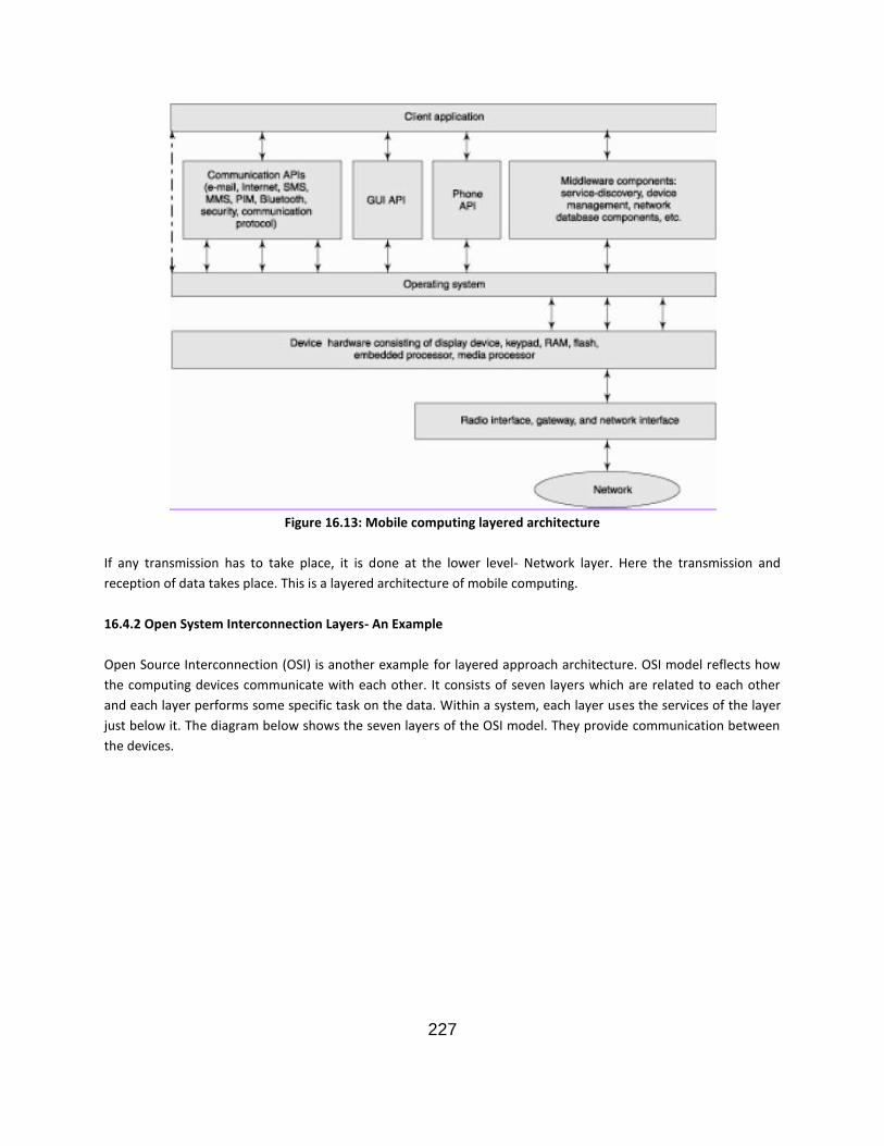
227
Figure 16.13: Mobile computing layered architecture
If any transmission has to take place, it is done at the lower level- Network layer. Here the transmission andreception of data takes place. This is a layered architecture of mobile computing.
16.4.2 Open System Interconnection Layers- An Example
Open Source Interconnection (OSI) is another example for layered approach architecture. OSI model reflects howthe computing devices communicate with each other. It consists of seven layers which are related to each otherand each layer performs some specific task on the data. Within a system, each layer uses the services of the layerjust below it. The diagram below shows the seven layers of the OSI model. They provide communication betweenthe devices.
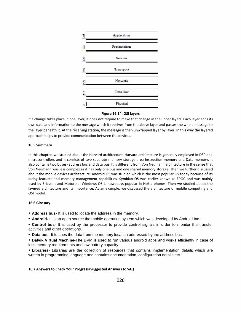
228
Figure 16.14: OSI layersIf a change takes place in one layer, it does not require to make that change in the upper layers. Each layer adds itsown data and information to the message which it receives from the above layer and passes the whole message tothe layer beneath it. At the receiving station, the message is then unwrapped layer by layer. In this way the layeredapproach helps to provide communication between the devices.
16.5 Summary
In this chapter, we studied about the Harvard architecture. Harvard architecture is generally employed in DSP andmicrocontrollers and it consists of two separate memory storage area-Instruction memory and Data memory. Italso contains two buses- address bus and data bus. It is different from Von Neumann architecture in the sense thatVon Neumann was less complex as it has only one bus and one shared memory storage. Then we further discussedabout the mobile devices architecture. Android OS was studied which is the most popular OS today because of itsluring features and memory management capabilities. Symbian OS was earlier known as EPOC and was mainlyused by Ericsson and Motorola. Windows OS is nowadays popular in Nokia phones. Then we studied about thelayered architecture and its importance. As an example, we discussed the architecture of mobile computing andOSI model.
16.6 Glossary
Address bus- It is used to locate the address in the memory. Android- It is an open source the mobile operating system which was developed by Android Inc. Control bus- It is used by the processor to provide control signals in order to monitor the transferactivities and other operations. Data bus- It fetches the data from the memory location addressed by the address bus. Dalvik Virtual Machine-The DVM is used to run various android apps and works efficiently in case ofless memory requirements and low battery capacity. Libraries- Libraries are the collection of resources that contains implementation details which arewritten in programming language and contains documentation, configuration details etc.
16.7 Answers to Check Your Progress/Suggested Answers to SAQ

229
1. In Harvard architecture, instructions and data are stored in different physical storage. While in von Neumannarchitectural scheme, instructions and data share same memory storage. The Harvard architecture comprises twoseparate buses- instruction bus and data bus while in von Neumann, both data and instructions are carried on thesame bus.
2. Data bus carries data from the memory.
3. Some of the libraries are-Surface Manager, Media Framework, SQLite, OpenGL, FreeType, WebKit,SGL, SSL and Libc.
4.The DVM is used to run various android apps and works efficiently in case of less memory requirements and lowbattery capacity. DVM is based on Just In Time compiler of Java. DVM allows multiple virtual machines to beexecuted on a single device in various processes which provides memory management, security etc.
5. DVM converts class files into .dex files.
6. Marshmallow
7. Uikon is a framework on top of which the user interfaces are built. It provides basic class libraries that createdifferent user interfaces and also it provides an interface to use services like alerts, notifications, display etc.
8. Various components in UI Toolkit are- graphics effects, UI graphic utilities, grid, BMP animation, clock andanimation.
9. Comms Service
16.8 Terminal and Model Questions
1. Explain Harvard architecture? Differentiate it with Von Neumann architecture?
2. Describe Android architecture and its features?
3. What are the basic features of Symbian OS and explain its architecture with suitable layered diagram?
4. Why layered approach is used in architecture? Explain an example.
5. What is DVM and its use?


