27
Image Sensor Pixel Cross-Sectional Analysis

Image Sensor Pixel Cross-Sectional Analysis

2Image Sensor Die Utilization Analysis
Some of the information in this report may be covered by patents, mask and/or copyright protection. This report should not be taken as an inducement to infringe on these rights.
© 2011 Chipworks Inc.
This report is provided exclusively for the use of the purchasing organization. It can be freely copied and distributed within the purchasing organization, conditional upon the accompanying Chipworks accreditation remaining attached.
Distribution of the entire report outside of the purchasing organization is strictly forbidden. The use of portions of the document for the support of the purchasing organization’s corporate interest (e.g., licensing or marketing activities) is permitted, as defined by the fair use provisions of the copyright act. Accreditation to Chipworks must be attached to any portion of the reproduced information.
EXM-1234-000JMRF
Revision: 1.0 Published: February 28, 2011
3Image Sensor Die Utilization Analysis
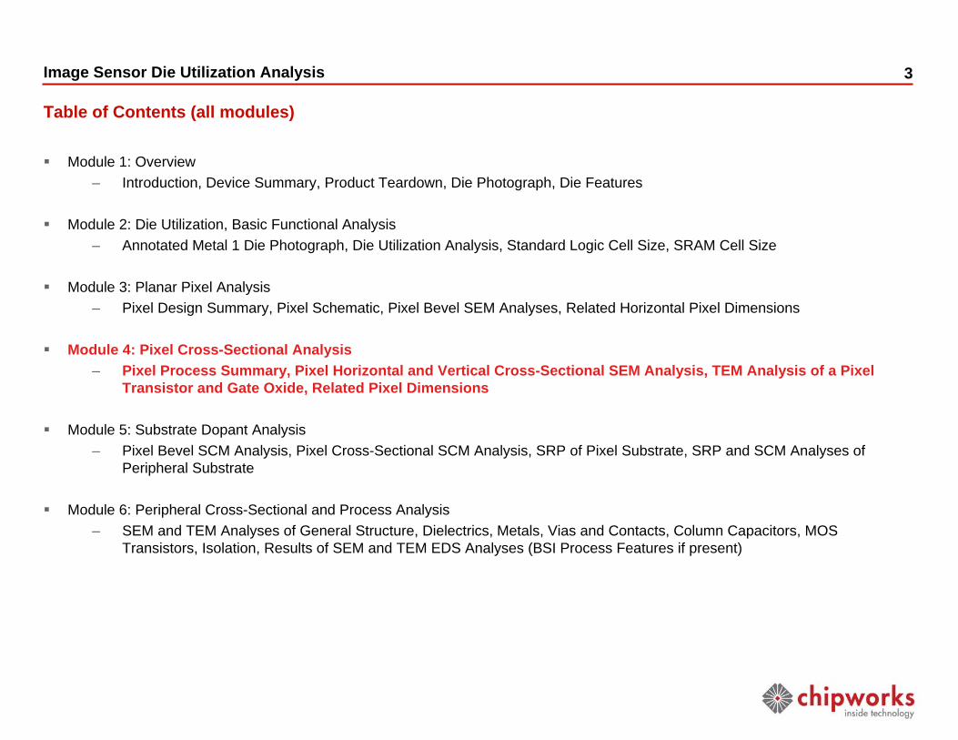
Table of Contents (all modules)
Module 1: Overview– Introduction, Device Summary, Product Teardown, Die Photograph, Die Features
Module 2: Die Utilization, Basic Functional Analysis– Annotated Metal 1 Die Photograph, Die Utilization Analysis, Standard Logic Cell Size, SRAM Cell Size
Module 3: Planar Pixel Analysis– Pixel Design Summary, Pixel Schematic, Pixel Bevel SEM Analyses, Related Horizontal Pixel Dimensions
Module 4: Pixel Cross-Sectional Analysis– Pixel Process Summary, Pixel Horizontal and Vertical Cross-Sectional SEM Analysis, TEM Analysis of a Pixel
Transistor and Gate Oxide, Related Pixel Dimensions
Module 5: Substrate Dopant Analysis– Pixel Bevel SCM Analysis, Pixel Cross-Sectional SCM Analysis, SRP of Pixel Substrate, SRP and SCM Analyses of
Peripheral Substrate
Module 6: Peripheral Cross-Sectional and Process Analysis– SEM and TEM Analyses of General Structure, Dielectrics, Metals, Vias and Contacts, Column Capacitors, MOS
Transistors, Isolation, Results of SEM and TEM EDS Analyses (BSI Process Features if present)
4Image Sensor Die Utilization Analysis
Module 4 Contents
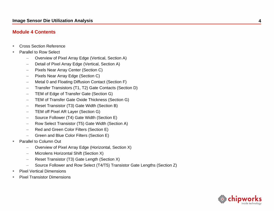
Cross Section Reference Parallel to Row Select
– Overview of Pixel Array Edge (Vertical, Section A)– Detail of Pixel Array Edge (Vertical, Section A)– Pixels Near Array Center (Section C)– Pixels Near Array Edge (Section C)– Metal 0 and Floating Diffusion Contact (Section F)– Transfer Transistors (T1, T2) Gate Contacts (Section D)– TEM of Edge of Transfer Gate (Section G)– TEM of Transfer Gate Oxide Thickness (Section G)– Reset Transistor (T3) Gate Width (Section B)– TEM off Pixel AR Layer (Section G)– Source Follower (T4) Gate Width (Section E)– Row Select Transistor (T5) Gate Width (Section A)– Red and Green Color Filters (Section E)– Green and Blue Color Filters (Section E)
Parallel to Column Out– Overview of Pixel Array Edge (Horizontal, Section X)– Microlens Horizontal Shift (Section X)– Reset Transistor (T3) Gate Length (Section X)– Source Follower and Row Select (T4/T5) Transistor Gate Lengths (Section Z)
Pixel Vertical Dimensions Pixel Transistor Dimensions

5Image Sensor Die Utilization Analysis
Analysis Sites
The die photograph is annotated to show the planes of SEM, TEM, and SCM pixel cross sections Subsequent SEM images are labeled with the cross section references (P2BSx)

6Image Sensor Die Utilization Analysis
Cross Section Reference
Pixel cross sections – poly

7Image Sensor Die Utilization Analysis
Overview of Pixel Array Edge (Vertical, Section A)
8Image Sensor Die Utilization Analysis
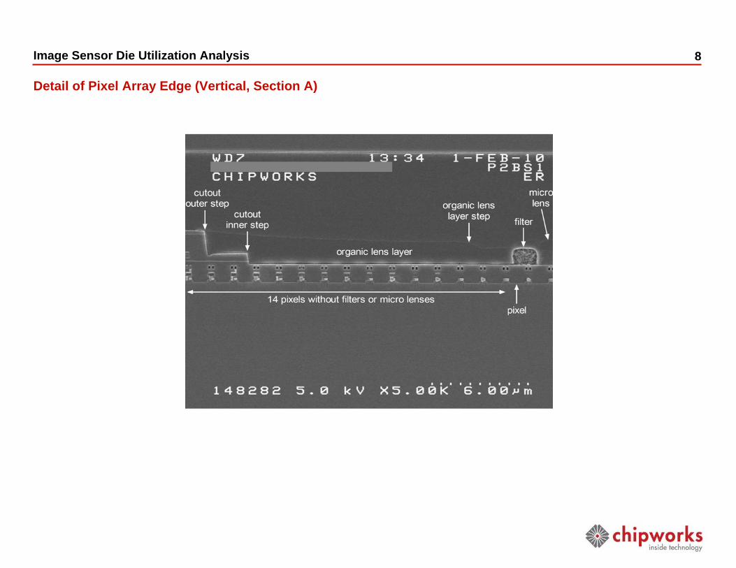
Detail of Pixel Array Edge (Vertical, Section A)
9Image Sensor Die Utilization Analysis
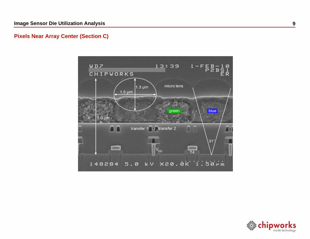
Pixels Near Array Center (Section C)
10Image Sensor Die Utilization Analysis
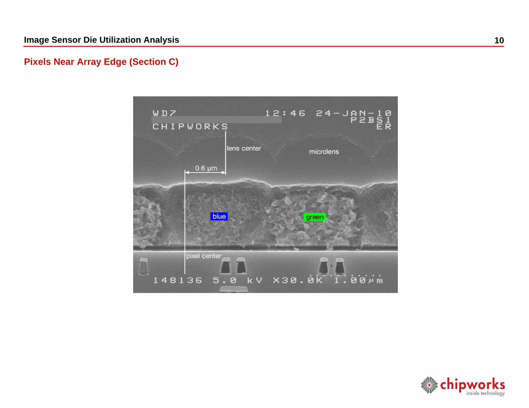
Pixels Near Array Edge (Section C)

11Image Sensor Die Utilization Analysis
Metal 0 and Floating Diffusion Contact (Section F)

12Image Sensor Die Utilization Analysis
Transfer Transistors (T1, T2) Gate Contacts (Section D)

13Image Sensor Die Utilization Analysis
TEM of Edge of Transfer Gate (Section G)
14Image Sensor Die Utilization Analysis
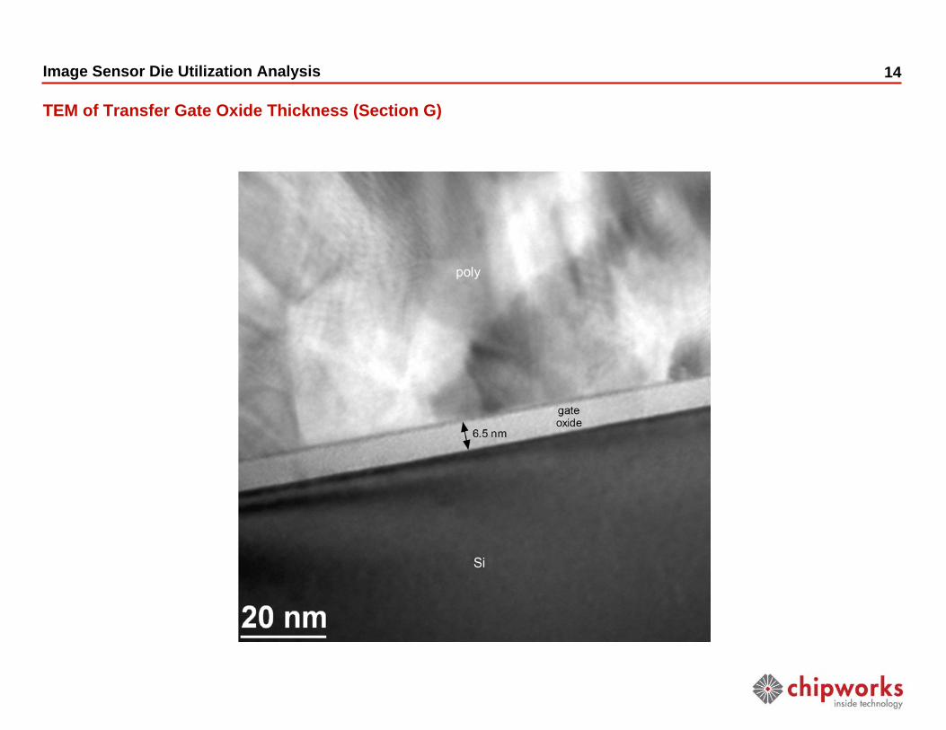
TEM of Transfer Gate Oxide Thickness (Section G)

15Image Sensor Die Utilization Analysis
Reset Transistor (T3) Gate Width (Section B)
16Image Sensor Die Utilization Analysis
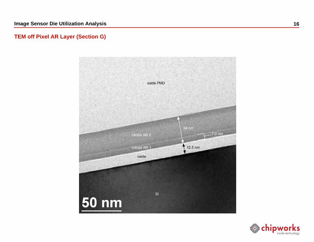
TEM off Pixel AR Layer (Section G)

17Image Sensor Die Utilization Analysis
Source Follower (T4) Gate Width (Section E)

18Image Sensor Die Utilization Analysis
Row Select Transistor (T5) Gate Width (Section A)
19Image Sensor Die Utilization Analysis
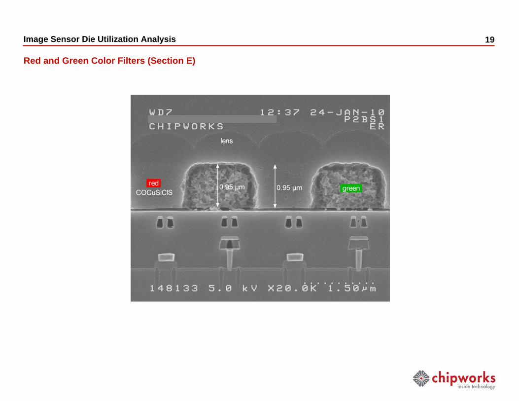
Red and Green Color Filters (Section E)

20Image Sensor Die Utilization Analysis
Green and Blue Color Filters (Section E)
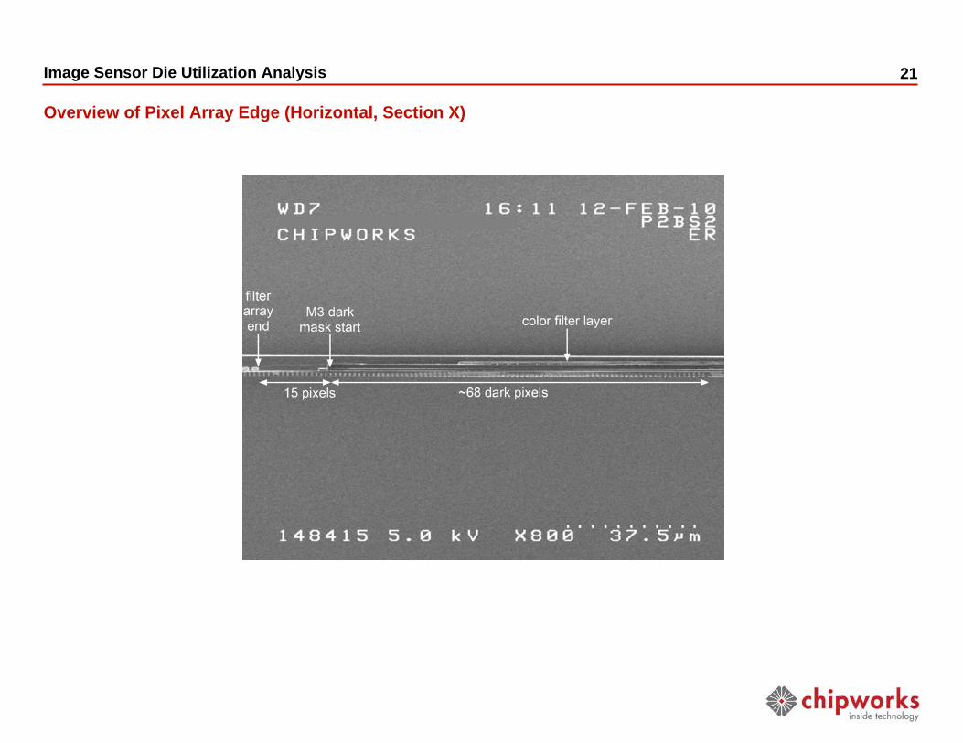
21Image Sensor Die Utilization Analysis
Overview of Pixel Array Edge (Horizontal, Section X)
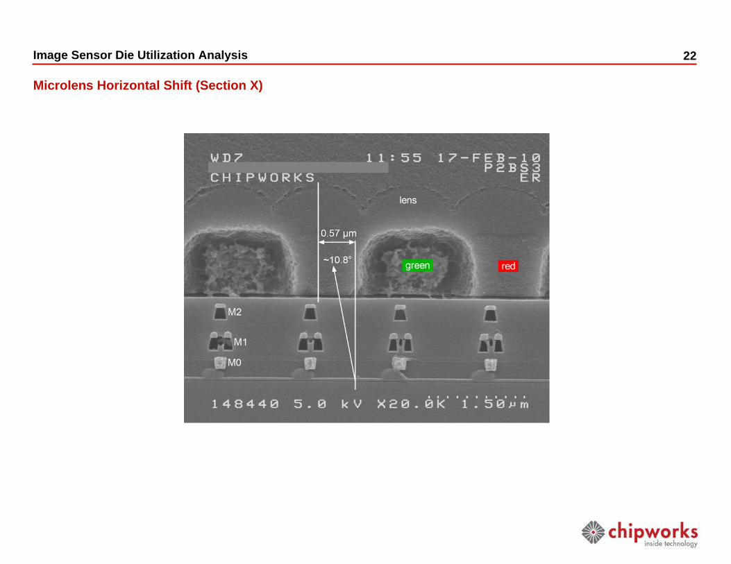
22Image Sensor Die Utilization Analysis
Microlens Horizontal Shift (Section X)
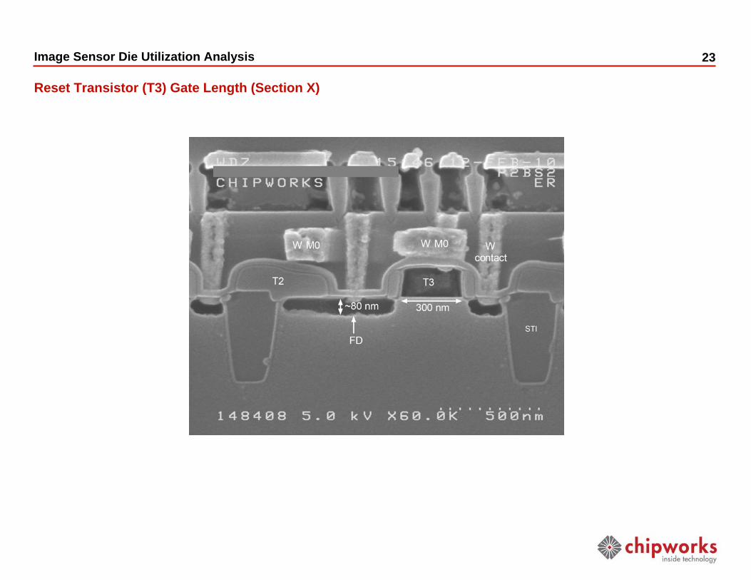
23Image Sensor Die Utilization Analysis
Reset Transistor (T3) Gate Length (Section X)

24Image Sensor Die Utilization Analysis
Source Follower and Row Select (T4/T5) Transistor Gate Lengths (Section Z)

25Image Sensor Die Utilization Analysis
Pixel Vertical Dimensions
31°Pixel field of view
0.90Red filter thickness
0.95Green filter thickness
1.0Blue filter thickness
11°Chief ray angle, vertical
15°Chief ray angle, horizontal (estimated)
34 nmPixel AR thickness
1.5/1.3Microlens major/minor axes (elliptical)
6.5 nmTransfer transistor gate oxide thickness
3.0Optical stack height (top of microlens to silicon substrate)
Dimension (µm)Feature

26Image Sensor Die Utilization Analysis
Pixel Transistor Dimensions
0.28
0.44
0.30
Variable (0.2 – 0.4)
Gate Length (µm)
0.24Row select (T5)
0.24Source follower (T4)
0.23Reset (T3)
Variable (0.35 – 0.65)Transfer (T1, T2)
Gate Width (µm)Transistor

27Image Sensor Die Utilization Analysis
About ChipworksChipworks is the recognized leader in reverse engineering and patent infringement analysis of semiconductors and electronic systems. The company’s ability to analyze the circuitry and physical composition of these systems makes them a key partner in the success of the world’s largest semiconductor and microelectronics companies. Intellectual property groups and their legal counsel trust Chipworks for success in patent licensing and litigation – earning hundreds of millions of dollars in patent licenses, and saving as much in royalty payments. Research & Development and Product Management rely on Chipworks for success in new product design and launch, saving hundreds of millions of dollars in design, and earning even more through superior product design and faster launches.
Contact ChipworksTo find out more information on this report, or any other reports in our library, please contact Chipworks at 1-613-829-0414
Chipworks3685 Richmond Road, Suite 500Ottawa, Ontario K2H 5B7 CanadaT 1-613-829-0414F 1-613-829-0515Web site: www.chipworks.comEmail: [email protected]
Please send any feedback to [email protected]


![Cross sectional study.pptx [Read-Only]...Descriptive cross-sectional study Analytic cross-sectional study Repeated cross-sectional study 7 Descriptive Collected number of cases and](https://static.documents.pub/doc/80x56/5f0c07f77e708231d43368fd/cross-sectional-studypptx-read-only-descriptive-cross-sectional-study-analytic.jpg)


