Imaging Metal Halide Perovskites Material and Properties at the Nanoscale
John M. Howard, Richa Lahoti, and Marina S. Leite*
DOI: 10.1002/aenm.201903161
for wide-ranging optoelectronic utiliza-tions. Today, the world record for a single-junction perovskite solar cell PCE stands at 25.2%,[5] comparable to Si- and GaAs-based systems that have experienced nearly half a century of development. Sim-ilarly, light-emitting diodes have exceeded 21% in external quantum efficiency,[6] a critical threshold for commercial usage. However, the primary challenge for the reliable delivery of power using perovskite PV is still related to the lack of material stability upon exposure to intrinsic and extrinsic factors,[7,8] including their meso- to microscale physical behavior.[9–11]
Perovskite materials have the ABX3 structure, where the A-site is most often occupied by methylammonium (MA or CH3NH3
+) or formamidinium (FA or CH(NH2)2
+), the B-site by lead (Pb2+) or tin (Sn2+), and the X-site with a halide
species, typically iodine (I−) or bromine (Br−), though chlorine (Cl−) is also used. Small concentrations of cesium (Cs+) and/or rubidium (Rb+) are often substituted for the organic cations to improve the stability of the resulting devices.[12–14] The choice of the inorganic B-site alters the tunability substantially, as proven in FA-based perovskites.[15] Finally, the stoichiometry of the X-site allows for control of the optical bandgap from 1.6 eV (pure iodine) to 2.3 eV (pure bromine), in the case of pure MA.[1]
In addition to their promise for optoelectronic devices, MHP materials display an interesting intersection of properties. While all MHP are semiconductors, many also exhibit ferroic properties: ferroelasticity or ferroelectricity depending on the composition and fabrication methodology. Further, in addition to their adequate electronic conductivity, they present high ionic conductivity (especially when illuminated[16]), as underscored by the myriad of studies on ion migration.[17] Additionally, unlike their ceramic counterparts such as barium titanate or calcium titanate, the hybrid organic–inorganic perovskites show insta-bilities on the timescales ranging from nanoseconds to days.[7] While some of these transient properties are benign, many of the changes are chemically irreversible and detrimental to device stability/performance. The scientific literature contains multiple reports of dynamic optical or electronic behavior due to one or many of the following environmental factors: oxygen,[18] water,[8] bias,[19] temperature,[20] and/or light.[9,21,22] Several of the most promising MHP materials are polycrystal-line thin films, and, accordingly, require measurements that can provide insight into these material properties at the length scale of constituent grains and grain boundaries.[11,23]
Metal halide perovskites exhibit optimal properties for optoelectronic devices, ranging from photovoltaics to light-emitting diodes, utilizing simple fabrication routes that produce impressive electrical and optical tunability. As perovskite technologies continue to mature, an understanding of their fundamental prop-erties at length scales relevant to their morphology is critical. In this review, an overview is presented of the key insights into perovskite material properties provided by measurement methods based on the atomic force microscopy (AFM). Specifically, the manner in which AFM-based techniques supply valu-able information regarding electrical and chemical heterogeneity, ferroelec-tricity and ferroelasticity, surface passivation and chemical modification, ionic migration, and material/device stability is discussed. Continued advances in perovskite materials will require multimodal approaches and machine learning, where the output of these scanning probe measurements is combined with high spatial resolution structural and chemical information to provide a com-plete nanoscale description of materials behavior and device performance.
J. M. Howard, Prof. M. S. LeiteDepartment of Materials Science and EngineeringUniversity of MarylandCollege Park, MD 20742, USAJ. M. Howard, R. Lahoti, Prof. M. S. LeiteInstitute for Research in Electronics and Applied PhysicsUniversity of MarylandCollege Park, MD 20742, USAR. LahotiDepartment of Chemical and Biomolecular EngineeringUniversity of MarylandCollege Park, MD 20742, USAProf. M. S. LeiteDepartment of Materials Science and EngineeringUniversity of CaliforniaDavis, CA 95616, USAE-mail: [email protected]
The ORCID identification number(s) for the author(s) of this article can be found under https://doi.org/10.1002/aenm.201903161.
1. Introduction
Metal halide perovskite (MHP) research into both light-collecting and light-emitting applications has exploded over the past decade. While the record-setting rate of increase in photovoltaic (PV) power conversion efficiency (PCE or η) may have initially driven the rapid advances, the flexible optical properties,[1] simple low-temperature processing,[2] and high defect tolerance[3,4] all combine to make these ideal materials
In this review, we provide an overview of the essential insight into nanoscale perovskite properties established by techniques based on the atomic force microscope (AFM), first introducing the essential methods along with their operating principles then discussing the knowledge they provide about MHP material properties. We begin with the information identified through electrical imaging, with a focus on the inter- and intragrain variations in both current and voltage. A discussion of chemical imaging follows this section, identifying how these characteri-zations have evidenced ion migration and nanoscale chemical variations at both surfaces and interfaces. We then describe the most recent data in support of both ferroelasticity and ferroelec-tricity, and indicate how multimodal approaches are essential in evaluating these fundamental properties. This discussion is fol-lowed by a section related to AFM investigations into the oper-ating mechanisms and effectiveness of chemical modification and passivation. After, we analyze the use of AFM to understand both ion migration and underlying stability in MHP absorbers. Finally, the opportunities to use the big data and artificial intel-ligence (AI) paradigms in elucidating these material properties and device performance are described before concluding with our outlook for how AFM will continue to advance our commu-nity’s understanding of perovskite’s fundamental properties.
2. Electrical Properties
Given that MHP are most often implemented in optoelec-tronics, electrical imaging methods are essential. Further, the highest performing solar cells incorporate polycrystalline absorbers with grains sizes from ≈100–1000 nm. Using AFM, both the surface morphology and the correlated electrical response can be captured simultaneously. Most often, imaging with an AFM (illustrated in Figure 1) is performed with a
John M. Howard is a Ph.D. candidate working in Prof. Leite’s group in the Department of Materials Science and Engineering at the University of Maryland–College Park. He obtained his B.S. in physics, B.S. in mathematics, and B.A. phi-losophy from the University of Massachusetts–Amherst in 2013. His research focuses on understanding the causes of
environmentally induced optical and electrical dynamics in metal halide perovskites using in situ microscopy methods.
Richa Lahoti is a Ph.D. student in Department of Chemical and Biomolecular Engineering at the University of Maryland–College Park and holds a visiting scholar position at the University of California, Davis. She received her B.S. in chem-ical engineering from the University of Alabama, Tuscaloosa, in 2018. Her
research focuses on determining fundamental photovoltaic properties of perovskite solar cell materials through state-of-the-art nanoscale characterization techniques.
Marina S. Leite is an Associate Professor in the Department of Materials Science and Engineering at University of California, Davis. Her group is engaged in fundamental and applied research on functional mate-rials for renewable energy applications, including the visualization of dynamic physical and chemical pro-
cesses at the nanoscale. The Leite group has realized pio-neering atomic force microscopy methods to advance the understanding of halide perovskites for optoelectronics.
nanometer-sized probe (radius of curvature in the range of 1–100 nm) brought in close proximity to the sample surface. The laser light reflected off the cantilever is measured by a quadrant photo diode. Deflection in the cantilever due to probe–sample interactions causes a corresponding change in the photo-diode signal, allowing for imaging of the sample morphology. In this section, we provide a brief overview of the operating
Adv. Energy Mater. 2019, 1903161
Figure 1. The basic operating principle of an atomic force microscope (AFM). A schematic of the typical experimental setup for AFM-based measurements, where the deflection of the probe registers the sample topography while also allowing for nanoscale measurements of electrical, chemical, and ferroic properties.
principles for both Kelvin probe force microscopy (KPFM) and photoconductive-AFM (pc-AFM), before describing the key insights these techniques have revealed.
Kelvin probe force microscopy allows for the imaging of a material’s contact potential difference (illustrated schematically in Figure 2a) and can be implemented in a variety of manners, ranging from contact mode[24] to noncontact heterodyne vari-ants.[25] For noncontact KPFM, the underlying principle con-sists of an electrically oscillated probe and a voltage feedback loop finding the DC bias, the contact potential difference (CPD or VCPD; see the top of Figure 2a), that nullifies this vibra-tion at each point. If the device is illuminated (bottom half of Figure 2a), an additional offset from the quasi-Fermi level split-ting adds to the CPD. Upon appropriate instrument calibration, the difference between the dark and illuminated conditions, often termed the surface photovoltage (SPV), yields the quasi-Fermi level splitting which is proportional to the material’s open-circuit voltage (VOC). Thus, KPFM can provide quantita-tive information about the VOC fluctuations across the scanned region, if properly calibrated.[10] This involves performing both J–V and KPFM measurements as a function of incident photon flux (ϕ), and requires quantification of the device external quantum efficiency (EQE0) and the area of illumina-tion (AKPFM). Then, the macroscopic VOC is written as
InEQE
InEQE
EQEOC
0
darkCPD
KPFM ,
cell 0
VnkT
q
q
JV
A
A
ϕ τ= ⋅ ⋅
= − ⋅ ⋅
⋅
λ θ (1)
where Jdark is the dark saturation current, τ is the transmission of the illuminating optics, Acell is the active area of the full PV
device, and EQEλ,θ is the EQE as a function of wavelength and angle of excitation.[10] Here, we provide only a brief description of the operating principles with a limited discussion of the ben-efits or drawbacks of any specific method, referring the reader instead to previously published articles[26] and books[27] on the subject. Instead, we focus on how KPFM can interrogate perov-skite materials in order to advance the understanding of their fundamental properties.
The utility of KPFM techniques in measuring perov-skite samples is displayed in Figure 2b, wherein frequency- modulated KPFM images of the CH3NH3PbI3 (MAPI) film capture the voltage variations across different grain bounda-ries and within the grains themselves.[9] The same perovskite sample displays >300 mV voltage variations across its surface. Similar sets of KPFM measurements on planar and inverted geometry perovskite films have established downward band bending at the grain boundaries as well as an increased affinity for electrons,[28] though the SPV behavior depends on the type of heterojunction.[29] Our group has realized heterodyne KPFM (H-KPFM) with a frame rate of 16 s to a scan region within a single grain, which enabled real-time and nanoscale measure-ments of the transient electrical response of a variety of perov-skites.[10,22] As marked with a white box in Figure 2bi, the CPD images are captured across an illumination cycle. Here, the fast acquisition of the heterodyne mode is enabled by detecting the CPD at a different frequency than the topographic feed-back loop and the applied AC bias.[25] The H-KPFM images are binned into histograms to more clearly quantify the persistence of the postillumination residual voltage. Unlike standard inor-ganic semiconductors, such as GaAs or Si, where charge carrier
Adv. Energy Mater. 2019, 1903161
Figure 2. Imaging contact potential difference (CPD) and surface photovoltage (SPV) with Kelvin probe force microscopy. a) The working principle behind dark and illuminated KPFM. Under dark conditions, the KPFM feedback loop finds the voltage corresponding to the material CPD at each pixel. When a semiconductor is illuminated, the quasi Fermi level splitting changes the CPD value, and the difference in values between dark and light condi-tions yields the SPV.[10] Reproduced with permission.[10] Copyright 2015, Wiley-VCH Verlag GmbH & Co. KGaA, Weinheim. b) A larger area i) topography and ii) KPFM scan of a MAPI3 perovskite. The white box shows the area where fast, heterodyne KPFM is used to image the iii–viii) CPD in real-time across an illumination cycle. Histograms of the KPFM maps acquired every 16 s reveal the slow voltage relaxation.[9] Reproduced with permission.[9] Copyright 2017, American Chemical Society.
generation ends in nanoseconds or less, MHP often display slow voltage relaxation processes.[21,30–32] While the underlying mechanism for the slow voltage decay will be explored in the later section on ion migration, the results shown in Figure 2b indicate the need for imaging techniques to elucidate the source of electrical heterogeneity.
As described in Figure 3a, pc-AFM consists of a circuit with one point of electrical contact made with the appropriate mac-roscopic contact and the second point of electrical contact made with a conducting AFM probe, rastering across the surface. In this manner, both the contact-mode topography and current are simultaneously recorded. In the case of a typical inverted perov-skite, the macroscopic contact usually is the fluorine-doped tin oxide (FTO), and the AFM probe contacts the perovskite film directly. The current is limited by both the probe geometry and the illumination conditions, and is not expected to reach levels similar to macroscopic J–V measurements. Measure-ments can also be made after subsequent passivation treat-ments to evaluate their efficacy, as discussed further in Section 2.3. While pc-AFM is more destructive to the probe, in com-parison to KPFM, it is arguably simpler, as current collection is determined by a single feedback loop maintaining the tip at a user-selected deflection. The current signal of the sample can be increased by either increasing the voltage applied to the sample or by increasing the illumination power density to generate more charge carriers. For the MHP, the application of voltage or light to amplify the signal must be done carefully, as the material properties may change during the measurement. Accordingly, many studies report topography images acquired without bias under dark conditions to establish that the sample was minimally altered throughout the course of the pc-AFM measurements.[9,33] The ambient environment of the perovskite sample is also a critical parameter, with many of the reported
measurements performed in a glove box or employing a flow cell to prevent undesired chemical reaction from taking place.
Exemplary images of a MAPI perovskite thin film are shown in Figure 3b. The topography is void of artifacts with grains ranging ≈100–500 nm in size, and the short-circuit condition dark and illuminated (70 mW cm−2) images show an order of magnitude difference in the current signal (≈4 and ≈40 pA, respectively). These current maps reveal the influence of grains and grain boundaries on current extraction and can be used to generate relevant statistics about the spatial distribution of the electrical response of perovskites. The influence of the grain boundaries under dark conditions is unclear, showing a uni-form response with a mean of 0.06 pA. However, under illumi-nated conditions, a number of the boundaries display increased conductivity with respect to the grains they enclose. Many of the boundaries are not detectable at all, revealing groups of grains uniformly generating current. Therefore, to obtain a full picture of the physical processes governing the spatial inhomogeneity captured by pc-AFM, correlated chemical[34] and/or structural[35] images should be performed. Independent pc-AFM measurements of an MAPI3−xClx perovskite reveal pos-sible facet-dependent current variations.[36] These results high-light an opportunity for optimizing the fabrication of the MHP layers such that grains display a more spatially homogenous current response closer to the highest recorded levels within the pc-AFM scan. Current imaging can be extended by simul-taneously biasing the sample, generating images as discrete voltages to infer the diode characteristic. Similar measurements can be made by performing I–V spectroscopy at each pixel of the image.[36] With either method, images for both effective maximum power output and effective VOC can be extracted. However, the VOC is often noisy in comparison to the ISC image, as it is typically computed by finding the bias condition yielding
Adv. Energy Mater. 2019, 1903161
Figure 3. Imaging dark and light generated current at the nanoscale with photoconductive atomic force microscope (pc-AFM). a) An overview of pc-AFM as applied to perovskites, where the AFM feedback loop maintains the conductive probe in contact with the perovskite layer at a constant force closing the circuit.[33] Reproduced with permission.[33] Copyright 2016, American Chemical Society. b) Examples of a MAPI3 film (i) topography along with images of (ii) dark and (iii, iv) light-generated current acquired at short-circuit conditions.[33] Reproduced with permission.[33] Copyright 2016, American Chemical Society.
a zero-mean current image. As we describe in the paragraphs above, KPFM is a complementary tool for capturing nanoscale voltage heterogeneity. Throughout this review, both pc-AFM and KPFM will prove critical for studying ferroic properties, surface passivation, ion motion, and material stability.
3. Chemical Imaging
A complete understanding of perovskite solar cells includes knowledge about material properties such as the chemical com-position of the perovskite layer. Peak force infrared microscopy (PFIR) is one possible scanning probe technique for resolving chemical information at the nanoscale.[37] This is a noninvasive method that embodies both chemical and mechanical imaging of the perovskite layer. PFIR acquires infrared spectroscopic information at each pixel with a spatial resolution of 10 nm, overcoming the shortcomings of Fourier transform infrared (FTIR). Briefly, this nanoscale technique functions with infrared laser pulses in a synchronized fashion, with changes in the cantilever deflection registered during the peak force tap-ping cycles with and without illumination. Infrared absorption data is generated by volume changes in the sample due to thermal expansion, and the difference between these two data sets gives the PFIR trace. This technique allows for phase sepa-ration and inhomogeneity investigation in CH3NH3PbBr3, as shown in Figure 4.[37] All chemical functional groups have a unique infrared light adsorption response, permitting chemical imaging. The topography image (Figure 4) reveals a nanocrystal protruding off the sample surface. The PFIR (Figure 4b) image indicates that different infrared frequencies are absorbed by the nanocrystal and a homogenous absorbance by the
supporting crystal surface below. Figure 4c,d further confirms the inhomogeneity (marked with a circle) in the nanocrystal by showing variations in the modulus and adhesion, respec-tively. The specific chemical composition (Figure 4e) of the nanocrystal was evaluated by comparing the PFIR spectra at the three different locations marked in Figure 4a to the mac-roscopic FTIR data. These spectra suggest degradation of the CH3NH3PbBr3 layer leading to small amounts of PbBr2 and variations in the density of methylammonium.
Another similar approach that has proven useful in iden-tifying chemical heterogeneity in MHP materials is photo-thermal induced resonance (PTIR or AFM-IR).[38] A typical setup for PTIR works as follows: i) a pulsed laser tuned to a relevant vibrational or electronic wavelength illuminates the perovskite sample deposited on a prism. The absorption by the MHP sample leads to local thermal expansion that can be inferred from the cantilever deflection. The spatial resolution for PTIR (50–100 nm) is not nearly as precise as PFIR. PTIR has been used to map the electromigration MA+ in MAPI cross sections[39] and evaluate the chemical origin of ferroelastic properties in perovskites,[34,40] with numerous open topics yet to be explored.
4. Ferroelectricity
In addition to their long carrier lifetimes,[41] tunable bandgap,[42] and high carrier mobility,[43] perovskites are proposed to dis-play spontaneous polarization originating from the alignment of the dipolar organic A-site cations.[44] A large number of theoretical and experimental studies have been carried out to understand the ferroelectric properties for various perovskite
Adv. Energy Mater. 2019, 1903161
Figure 4. Inhomogeneities at CH3NH3PbBr3 surfaces revealed by peak force infrared (PFIR) microscopy. a) Large CH3NH3PbBr3 nanocrystal (500 nm × 300 nm) on the surface shown in a topography map obtained using AFM. b) PFIR map: large variations in signal strength can be seen across the nanocrystal. Infrared frequency: 1585 cm−1. c) Modulus image showing loss of mechanical modulus at the discontinuous nanocrystal with the d) adhesion data further showing inhomogeneity. e) PFIR spectra collected at three locations (marked in (a)) in agreement with the Fourier transform infrared resonance (FTIR) spectra. f) 12 nm spatial resolution of PFIR from the red line marked in (b).[37] Reproduced with permission.[37] Copyright 2017, AAAS.
compositions and fabrication routes. Here, we summarize the key results from the literature without taking a side on the ongoing debate over which ferroic properties are actually displayed by MHP.
Nanoscale measurements are inherent to investigations into ferroelectric materials, and, accordingly, AFM plays a fundamental role. PFM is an effective technique for investi-gating ferroelectric materials because the non-centrosymmetric crystal classes form a hierarchy, where each subset also shares the properties of the larger group. The piezoelectric mate-rials display a voltage in proportion to external stress. The pyroelectrics, in addition to displaying all the piezoelectric characteristics, also have a built-in dipole. Thus, the surface of the material maintains a charged state dependent on tem-perature. Finally, the ferroelectrics, another subset inheriting the traits of the pyroelectrics and piezoelectrics, also exhibit spontaneous polarization below their Curie temperature. The total free energy of ferroelectric crystals is minimized through the formation of alternating domains. Piezoresponsive force microscopy (PFM), a contact mode method, is a standard AFM-based tool for directly imaging the alternating pattern. PFM operates according to the converse piezoelectric effect, wherein an applied voltage induces a strain in the material under test. In the case of PFM, an AC voltage is applied to the conductive tip held at a constant force, and the tip records the local material deformation. The material will expand or con-tract depending on the polarity of the ferroelectric domain. PFM can be implemented to measure out-of-plane (vertical
PFM or V-PFM) and both in-plane (lateral PFM or L-PFM) deformations.
Figure 5 displays a multimodal approach to detecting ferro-electricity in a polycrystalline MAPI thin film. In this study, the film consisted of an ITO bottom electrode, a PEDOT:PSS elec-tron transport layer, and a spin-coated MAPI film of 300 nm, with all of the AFM measurements performed inside a nitrogen-filled glove box. The representative topography (Figure 5a) shows grains ranging from 500 to 3000 nm in diameter. The ferroelectric domains are not observable in the topography map. Figure 5b (L-PFM) and d (H-PFM) reveals that the ferro-electric domains are strongly present in the L-PFM images, but only faintly for the H-PFM mode. Based on the line profiles extracted from the L-PFM image, the authors concluded that the ferroelectric domains were approximately 90 nm in width. Finally, the KPFM image (Figure 5c) shows that the ferroelec-tric domains negligibly alter the CPD response. The possibility of MAPI being just a piezoelectric material was discounted, as piezoelectric materials do not form alternating domains within a single grain. Investigating the most promising perovskite com-positions for PV remains challenging, as large poling biases did alter the material through ion (discussed later; see Section 2.4) or even proved destructive due to the thermal effects of high cur-rent density.[39] Electron microscopy results have been applied to complement the analysis presented by showing that the striping pattern extends throughout the material bulk.[45] While studies have shown that these ferroelectric domains exist in absorbers incorporated into high-performing solar cells, the impact of
Adv. Energy Mater. 2019, 1903161
Figure 5. Investigating perovskite ferroelectricity with piezoresponsive force microscopy (PFM). a) Topography, b) lateral PFM (L-PFM), c) KPFM, and d) vertical PFM (V-PFM) deconvolute the film’s ferroelectricity from the surface potential and topography.[46] Reproduced with permission.[46] Copyright 2019, The Authors.
ferroelectricity on the electrical properties remains an open question.
Other research groups have been independently investi-gating ferroelectric properties and domain polarization to understand the influence on perovskite PV behavior, using MAPI single crystals as a model experimental system.[47] In this report, a new dual technique termed band excitation pie-zoresponsive force microscopy with concurrent contact Kelvin probe force microscopy (BE-PFM/cKPFM) is implemented.[48] Band excitation AFM approaches overcome the standard limi-tations of single-frequency measurements, by simultaneously driving the probe, whether mechanically or electrically, across a range of frequencies centered around the cantilever reso-nance. Given our focus on the nanoscale properties of MHP, we do not provide a comprehensive review of BE AFM tech-niques, instead directing the reader to the existing literature.[49] The cKPFM method consists of first applying a “write” DC bias to the sample followed by a lesser read DC bias to detect any change due to the prior step.[24] The BE-PFM detection occurs simultaneously, measuring the oscillating strain induced by the cKPFM voltages. The on-field BE-PFM response for the MAPI single crystal, extracted by fitting a simple harmonic oscillator (SHO), is shown in Figure 6a, where the “write” voltage is cycled between −15 and 15 V with the colors corresponding
to the different cKPFM “read” biases. The on-field response reveals the material’s polarization state.
The BE-PFM/cKPFM approach is then correlated with both scanning microwave impedance microscopy (sMIM) and elec-tric force microscopy (EFM) to measure how the ferroelectric response changes the electronic properties and material sta-bility. The contact-mode sMIM technique determines the local changes in capacitance (dC/dV) for the AC voltage applied to the tip and indicates charge carrier concentration and doping type. The sMIM dC/dV amplitude image in 67b reveals that the positively oriented domain is associated with a lower charge carrier concentration, while the corre-sponding dC/dV phase image identifies the n-type doping of the same stripe. While the topography image in Figure 6d exhibits the striped domain, the ferroelectric domains only impact the electrical response of the material if sufficiently biased. Figure 6e presents the EFM image as well as characteristic topography (dashed black line) and EFM amplitude (red 0 V, blue 8 V) line scans. Clearly, the EFM response is not coupled to the topography, as the patterning only emerges at 8 V and is anticorrelated with the topography. Finally, the stability of the ferroelectric domains was evaluated by exposing the sample to ambient air for three weeks and then by remeasuring the surface topography. The topography image in Figure 6f shows that the
Adv. Energy Mater. 2019, 1903161
Figure 6. Ferroelectric domains impact the local electrical response. a) The BE-PFM response recorded while the cKPFM “write” bias is applied shows the existence of two distinct bands corresponding to the polarization states. The “read” voltage value is given by the color bar below the plot. The sMIM b) amplitude image reveals the lower charge carrier concentration of the positive ferroelectric domains, while the c) sMIM phase map reveals the same positive domain as n-type. d) The topography image reveals the characteristic domains and e) electrostatic force microscopy (EFM) of the dashed region in (a) performed at 8 V indicates that the domain boundaries change the electrical response depending on bias state. f) The topography image after three weeks under ambient conditions shows the persistence of the ferroelectric domains.[47] Reproduced with permission.[47] Copyright 2019, The Authors.
domains persist, with air preferentially etching the oppositely oriented domains. Together, these results strongly suggest that MAPI is a relaxor ferroelectric material, exhibiting spontaneous polarization possibly due to nanoscale chemical variations.
While many of the reports of ferroelectricity investigate MAPI thin films or single crystals, the body of work exploring the ferroic properties in FA-based or mixed-cation (Cs and Rb) is less mature. Given that mixed-cation perovskites are often more stable and equally efficient, their fundamental proper-ties must be comprehended in order to build long-term stable devices. Similar measurements should also be carried out on fully inorganic and Pb-free compositions, especially now that the former has exceeded 17% efficiency.[50] Recently, triple-cation (CsFAMA) perovskite thin films were evaluated using direct piezoresponsive force microscopy (d-PFM)[51] and the results reported indicate this composition is not ferroelectric.[52] In this variant of PFM, a current-to-voltage transimpedance amplifier records the charge induced by the force of the tip. Thus, d-PFM directly measures the converse piezoelectric effect and the corresponding tensor coefficients. To understand fer-roelectricity in the CsFAMA perovskite, the d-PFM technique was first applied to periodically poled lithium niobate (PPLN), a known piezoelectric material, and then to the perovskite film. The d-PFM imaging is sensitive to scan direction, with the recorded current at domain boundaries inverting between the two scan directions. Unlike the PPLN sample, the triple cation perovskite does not exhibit any notable differences for the two scan directions presented in Figure 7a,b.
The imaging of piezoresponsivity in the CsFAMA perovskite is complemented by time-dependent current measurements, where the force applied by the AFM probe proceeds through a user-defined ramp profile (see the black curve in Figure 7c). For standard piezoelectric materials, an increasing force will induce a charge build-up that quickly dissipates once the force stabilizes. Interestingly, the mixed-cation perovskite shows an increase in current when the force is ramped up to 226 µN. Unlike the PPLN, the recorded current does not decay while the force is held at 226 µN. When the force is reduced to 20 µN, the current values slowly decrease (150 ms time constant), as shown in Figure 7d. Compared to the equivalent data on PPLN, where the current dissipates as quickly as the amplifier can register, the CsFAMA perovskite’s decay is incredibly slow, and not in line with the timescales associated with the structural deformation in piezoelectrics. Instead, the slow current decay is attributed to ion migration, which is influenced by the amount of force applied by the tip. In comparison to traditional PFM, the DPFM technique is less sensitive to measurement artifacts, and equiva-lent measurements on MAPI films of different grain sizes and fabrication routes did not present ferroelectricity either.
5. Ferroelasticity
In addition to their semiconductor nature, MHP are posited to exhibit ferroelasticity that may impact current extraction and the hysteretic J–V behavior. Accordingly, both electrical and chemical
Adv. Energy Mater. 2019, 1903161
Figure 7. Ferroelectricity-free mixed-cation (CsFAMA) perovskite films. Direct piezoresponsive force microscopy (DPFM) imaging reveals no change in current with a,b) scan direction, unlike common piezoelectric materials. c) Current and force versus time for the same CsFAMA perovskite, displaying a nonzero current for a constant applied force. d) Current as a function of time showing the slow recovery of the current signal between the vertical dashed red lines in (c) following the reduction in the tip force, uncharacteristic of piezoelectric materials.[52] Reproduced under the terms of the CC-BY license.[52] Copyright 2019, RSC. The Royal Society of Chemistry.
imaging are critical to fully understand the ferroic properties of these promising materials. In this section, we discuss prior reports of ferroelasticity, the existence of spontaneous strain, in MHP materials as investigated with the AFM. For example, using BE-PFM, researchers were able to identify that the com-monly reported striped domains likely have different associated resonance frequencies.[34] In this work, scanning electron micro-scopy (SEM) confirmed the presence of twin domains, revealed to be variations in CH3NH3
+ through the application of Helium ion microscopy with secondary ion mass spectroscopy (HIM-SIMS). PTIR, as described above, has established local chem-ical variation in the twin domains of CH3NH3PbI3 perovskites. Figure 8a,b shows the topography and chemical map for MA+ density distribution for the MAPI sample. Similar measurements using two-photon total internal reflection fluorescence micros-copy identified differences in the crystallographic orientation between the twin domains. A line profile of the MA+ gradient along the black dashed line in Figure 8b is given in Figure 8c. The graph shows the periodic nature of ion distribution within the twin domain, characteristic of ferroelastic materials.
The formation of twin domains occurs as a result of internal strain generated by the ferroelastic phase transition.[53] To offset the strain, twin domains form in the direction of dif-ferent crystallographic planes. Thus, these twin domains have a periodic pattern oriented parallel or sometimes perpendic-ular to each other. Prior efforts have found periodic MA+ ion segregation in twin domains and different crystallographic orientations of ferroelastic domains.[34,40,53] The chemical seg-regation has been attributed to the nonuniform distribution of strain within the material,[34] leading the authors to conclude that the investigated MHP material is ferroelastic and not fer-roelectric, as the domains formed only as a result of applied strain. External stress produces spontaneous strain, which causes the simultaneous presence of different orientation states that induce ferroelasticity.[40,53] Strain application analyses of both polycrystalline and single crystal MAPI samples helped identify typical ferroelastic behavior; strain-stress plots show nonlinear and hysteretic behavior.[34] Further evaluation of fer-roelastic twin domain is essential to learn about mechanical hysteresis, conductive domain walls, and the impact on dif-fusion lengths for charge carriers.[53] To aid the resolution of the ongoing debate surrounding the existence of ferroelasticity versus ferroelectricity,[54,55] we suggest i) research groups use standard fabrication methods for both polycrystalline films and single crystals to minimize sample-to-sample variation, ii) multimodal imaging experiments where BE-PFM and
d-PFM maps are combined with electron backscatter diffraction (EBSD) imaging to quantify the impact of crystal structure on the changes in cantilever resonance frequency.
6. Chemical Modification and Passivation Treatments
The instabilities of MHP solar cells are well researched, and there is substantial scope for improvement in areas such as photoabsorbance,[56] conductivity,[57,58] hysteresis,[59] and overall stability. Specifically, grain boundaries in perovskite solar cells (PSC) are infamous for their instability while perovskite layers are subject to recombination losses and hysteresis.[56] Changing the fabrication methodology for the perovskite layer through either chemical modification or surface passivation can sub-stantially improve perovskite absorber stability.
The concentration of PbI2 at the MHP surface can be con-trolled by changing the ambient moisture concentration during fabrication and alters both the surface potential and charge carrier extraction.[56] While humidity is known to degrade PSCs, preparing perovskite thin films in a moisture-controlled set-up creates a PbI2 rich phase at the GBs, confirmed with AFM, as well as SEM and transmission electron microscopy (TEM). KPFM and c-AFM techniques are critical to identify the changes in CPD and current in grain boundaries and interiors. Figure 9a shows the surface topography, current maps, and current distributions for two samples: i) one reference sample fabricated without passivation (in an inert N2 environment), and the ii) other with moisture-assisted passivation (30% rH), creating PbI2 rich phases at the grain boundaries.[56] The cur-rent maps demonstrate that the passivated sample produces higher current levels throughout the grain interiors while the reference sample presents higher current values at its bounda-ries. The current distribution histogram (Figure 9av) shows two peaks for the passivated sample, where the smaller peak represents the grain boundaries and the larger peak the grain interiors. With respect to the reference sample, the passivated sample generates higher current levels overall. Interestingly, the reference sample does not present a bimodal distribution, with the large peak attributed to the grain boundaries. These results highlight an opportunity for further optimization of the extent and duration of moisture passivation, in order to obtain the most spatially uniform production of current.
Chemical additives are another promising passivation route for achieving stable perovskite photovoltaics. By introducing
Adv. Energy Mater. 2019, 1903161
Figure 8. Capturing MA+ density fluctuations in MAPI twin domains. a) Topography image of MAPbI3 and corresponding b) PTIR chemical map of MA+ with average domain width of 206 nm calculated using the line in the image. c) A profile analysis along the line shown in the chemical map shows the distribution of MA+ ions. Infrared frequency: 1400 cm−1. Scale bar: 0.5 µm.[34] Reproduced with permission.[34] Copyright 2018, Nature Springer.
PCBM into the perovskite during fabrication, the electrical impact of common defects, such as the PbI3
− antisites, can be reduced.[59] With this strategy, PCBM is deposited homogene-ously throughout the MHP depth, residing primarily at the grain boundaries to form a mixed PCBM-perovskite material. PCBM passivation at grain boundaries reduces anion migra-tion, lowering hysteresis and improving device functioning. To confirm these findings, transient photoluminescence, transient photovoltage, and c-AFM were used. Transient photovoltage measurements identified that the introduction of PCBM into the perovskite films increases charge carrier lifetime, in com-parison to pure perovskite films. Transient photoluminescence spectroscopy indicated strong electron extraction for samples with sufficient ratios of PCBM to perovskite. Juxtaposing the current and topography images for both the pure and mixed perovskite sample shows concentrated high currents at GBs of the mixed perovskite sample (Figure 9bi,v). The order of magni-tude increase in current shown by the mixed-perovskite sample is due to the highly conductive nature of the PCBM. Conduc-tive AFM I–V analysis on pure perovskite (Figure 9bii–iv) and
mixed PCBM-perovskite films (Figure 9bvi–viii) confirmed that in the mixed film, the hysteresis effect is suppressed whereas hysteresis is quite prevalent in the pure perovskite film due to unsuppressed ion motion.
Charge carrier collection in PSCs can also be improved by integrating graphene nanonetworks within the perovskite (MAPbI3/G-NH2).[57] Here, the graphene nanonetwork pro-vided an increase in the area for conductance and charge carrier extraction. Incorporation of the G-NH2 network raises the overall PCE to 18.7%, compared to the 14.4% presented by the control device. This increase in power output occurs despite the two-fold reduction in PL lifetime, indicating an opportunity for further improvement. SEM indicates larger grains for the hybrid films, while TEM images reveal the presence of amor-phous grain boundaries with higher concentrations of G-NH2. Figure 10a shows the topography and c-AFM current images and current profiles for the MAPbI3 control and MAPbI3/ G-NH2 thin films. The MAPbI3/G-NH2 has a higher average current (301 pA vs 198 pA) concentrated at the grain bounda-ries, as revealed by the line profile data shown in Figure 10aiii,iv.
Adv. Energy Mater. 2019, 1903161
Figure 9. Improving current extraction with chemical modification. a) c-AFM reveals the impact of moisture-assisted fabrication. Topography and cor-responding c-AFM current images for samples fabricated under i,iii) pristine and ii,iv) 30% rH conditions. v) The current distribution from both c-AFM images is quantified by the histogram.[56] Reproduced with permission.[56] Copyright 2018, American Chemical Society Applied Material Interfaces. b) PCBM-perovskite hybrid absorbers exhibit reduced I–V hysteresis. c-AFM data overlaid the corresponding topography maps for i) the MAPI con-trol and v) PCBM–MAPI hybrid thin films. A sequence of nanoscale I–V curves under increasing negative bias for the ii–iv) MAPI control and vi–viii) PCBM–MAPI hybrid reveals the reduction in hysteresis for the latter.[59] Reproduced with permission.[59] Copyright 2015, Nature Springer.
The higher concentration of current at the grain boundaries corroborates with the TEM measurements identifying higher G-NH2 content at the grain boundaries. The MAPbI3/G-NH2 displays a more spatially heterogeneous current signal.
Other fabrication routes nullify the detrimental effects of MHP grain boundaries through a Lewis acid-base adduct method.[58] It consists of a nonstochiometric approach with the presence of excess CH3NH3I (MAI) that leads to a self-forming grain boundary with higher MAI content (confirmed with STEM with selected area electron diffraction). Time-resolved PL revealed that excess MAI, and the associated self-forming grain boundaries, increased the radiative recombination lifetimes,[60] until reaching 10 mol% upon which performance degrades. Figure 10bi,ii shows the topography (insets) and c-AFM (meas-ured at 2 V) results for equivalently sized regions for the 0 and 6 mol% excess of MAI conditions. While the stoichiometric film exhibits uniform current production, the self-forming grain boundaries have increased current levels. The MAI pre-sent at the grain boundaries passivates defects promoting charge carrier extraction. The macroscopic J–V characteristics (Figure 10biii) show reduced hysteresis and higher power con-version efficiency. KPFM images from other reports have found that excess MAI may produce perovskite surfaces with lower CPD values when compared to films produced with PbI2/MAI greater than one.[61] Cross-sectional SPV measurements show that the PbI2/MAI molar ratio in planar MHP solar cells con-trols the concentration of electron (holes) and, thus, the loca-tion of the diode junction.[62] The extent of J–V hysteresis can be controlled by engineering a PbI2-rich interfacial region that
serves to balance the electric field generated by the mobile ions accumulated nearby.[63] The results outlined in this sec-tion highlight the ability of AFM functional imaging to iden-tify the impact of fabrication optimization. Nanoscale electrical and chemical mapping will be crucial during the next decade of MHP development, as the community searches for synthesis pathways that increase material stability.
7. Ion Migration
Ion migration plays a critical role in the electrical and optical properties of MHP materials of many different compositions. AFM-based techniques have provided powerful insight into ionic motion at perovskite surfaces and interfaces, revealing how grain and their boundaries influence the rates of migra-tion. Other tools, such as photoluminescence[64,65] and open-cir-cuit voltage decay measurements,[30,31] are powerful, but cannot correlate the impact of mobile ions on surface morphology and the local electrical response. In this section, we detail a key subset of the scanning probe experiments that uncover ion migration occurring at the nanoscale and its impact on the material’s electrical properties.
Our research into MAPI perovskites has revealed that ion motion occurs at different rates across the perovskite surface. To understand how ion migration alters the electronic response, H-KPFM was applied over the course of an illumination cycle. Figure 11a–e displays the topography and corresponding VOC maps (the initial dark CPD image has been subtracted from
Adv. Energy Mater. 2019, 1903161
Figure 10. Increasing grain boundary current extraction with graphene additives or excess precursors. a) Effect of nanonetworks on perovskite layer conductivity. Comparison between pure MAPbI3 and MAPbI3/G-NH2 thin films. For each, topography, corresponding current map and current line profiles are shown. Scale bar: 400 nm.[57] Reproduced with permission.[57] Copyright 2018, RSC. b) High current observed at self-formed grain bounda-ries. Two different spatial topographies and their corresponding current maps are shown. Forward and reverse bias scan for one area is shown as a function of current density. Scan rate: 6 mV s−1.[58] Reproduced with permission.[58] Copyright 2016, Nature Springer.
all subsequent measurements) at various times after the illumination source has been switched off. The topography images reveal that the atypical electronic response for an illumi-nated semiconductor is not due to any emerging morphological features. The CPD scans present two distinct voltage relaxation timescales, evidenced by the residual plotted in Figure 11f. Here, the average voltage value of the map is given by the plot marker with the error bar showing three times the image standard deviations. The blue region presents negligible voltage decay, similar to the behavior of inorganic semiconductors such as Si or GaAs. However, the red voltage values take greater than 120 s to decline by ≈180 mV and finally equilibrate.
The contribution of mobile ions to the voltage response of the material can be modeled by the addition of an ionic current term to the standard diode equation for PV. The ionic current follows an exponential decay, as shown in Figure 11g, and counteracts the dark current, accounting for the observed residual voltage. While open-circuit voltage decay (OCVD)[30,66,67] and macroscopic Kelvin probe[68,69] measure-ments can perform equivalent measurements, the results pre-sented in Figure 11 underscore the need for spatial resolution on the length scales of the constituent grains. As shown, the impact of ion migration is a spatially heterogeneous process, indicating that some grains are structurally and/or chemically resistant to vacancy-mediated migration. Our results call for
high spatial resolution chemical and structural analyses on identical materials,[35,70] following the precedent set by several prior works.[34,37,39]
Scanning probe microscopy can also provide insight into interfacial processes, providing direct evidence of the impact of ion migration on the voltage response. To study the MAPI perovskite cross section, a forced ion beam lift-out process was applied to a MA0.17FA0.83Pb(Br0.17I0.83)3 perovskite solar cell. A 2 µm Pt capping layer protected the photoactive layers during the Ga-ion milling, and the J–V characteristic remains unchanged. Time-resolved KPFM spectroscopy was then applied point-by-point across the imaged region, after which the KPFM images are reconstructed, as shown in Figure 12ai,ii for light ON and light OFF, respectively. The average ΔCPD profiles for both illumination conditions are shown in Figure 12iii,iv. Within 2.5 ms of the illumination being switched ON, an 870 V cm−1 electric field arises across the interface, as quanti-fied by the linear fit (dashed black line). After 2700 ms, the elec-tric field has dissipated, though the voltage displays a ≈35 mV offset from the initial dark value that takes 1.5 s to equilibrate after turning OFF the white light (Figure 12iv). These results indicate that the perovskite–SnO2 interface charging strongly influences the observed voltage dynamics, acting as a source of iodide and iodide vacancies that alter interfacial recombina-tion.[71] Further, bias-dependent measurements performed on the
Adv. Energy Mater. 2019, 1903161
Figure 11. Probing ion migration with KPFM. a–e) Topography (top row) and real-time KPFM (bottom row) measurements within a single MAPI3 grain. f) The blue and red regions exhibit distinct voltage relaxation timescales corresponding to an additional current term in the g) diode equation due to ion motion.[9] Reproduced with permission.[9] Copyright 2017, American Chemical Society.
same samples exhibited similar timescales and CPD profiles, cor-roborating the influence of ionic migration and interfacial charging.
The occurrence of ion migration and its influence on the elec-trical response is best documented for the archetypal MAPI, yet is evident in perovskites with different composition and/or struc-ture. Figure 12b, for example, displays the results for the fast free time-resolved electrostatic force microscopy (FF-tr-EFM) as applied to a Ruddlesden−Popper (R–P) metal halide perovskites formed with butylammonium cations, with a film composition of (C4H9NH3)2PbI4 (abbreviated “BAPI”).[74] An R–P perovskite consists of multiple 2D layers, and are often more moisture-stable than comparable 3D systems.[75] Further, the R–P sys-tems display ideal electronic properties with exciton binding energies orders of magnitude higher than similar 3D compo-sitions.[76] Accordingly, a BAPI film was studied to understand if the superior stability was a result of the reduced ion motion and a more spatially uniform electrical response. The noncon-tact tr-EFM technique consists of monitoring the resonance shift of the AFM probe as photogenerated charge carriers build up in the material.[77] The decay in the capacitance between the tip and absorbing material after the light pulse is inversely proportional to the macroscopic EQE.[78] Thus, for solar cells, tr-EFM provides direct insight into the spatial variations in photocurrent. The “fast free” prefix refers to the fact that, in this operating mode, the cantilever scans without feedback with all probe dynamics recorded, analogous to G-mode KPFM.[79,80] The images are then constructed by fitting the probe dynamics to the appropriate model. The BAPI film topography (Figure 12bi) shows com-pact grains ≈2 µm in diameter with roughness in the range of ≈100 nm. The FF-tr-EFM lifetime (Figure 12bii) reveals that the grain boundaries build up charge nearly twice as slowly. Despite the slower dynamics, the grain boundaries display greater charge buildup, as indicated in the frequency shift in Figure 12biii. To
explain this spatial heterogeneity, a photoinduced field at the grain boundaries is proposed. The screening of this electric field along with higher trap densities leads to slower charge buildup.
The time-dependent dynamics have also been studied in solution-grown MAPbBr3 (also MAPBr3) single crystals using KPFM in ultrahigh vacuum. The topography of the scalpel-cleaved sample is given in Figure 13a, displaying the smooth, terraced morphology corresponding to individual MAPBr3 layers.[81] The white dots are the result of defects, either intrinsic or due to modification by the ambient atmosphere. The zoom-in region (black dashed line) is quantified in the histogram shown in Figure 13b, where the red line is a multi-Gaussian fit indicating a terrace height of ≈0.6 nm. The time-dependent SPV response of the MAPBr3 sample is captured in Figure 13c, where point measurements were used to collect time-series data before, during, and after two 60 s illumination treatments using 2.95 mW cm−2 of 515 nm light. When the light is first turned ON, the stabilization of the SPV signal takes five times longer (time constant of 11.4 s, as extracted from the exponential decay given by the black dotted line) than the sub-sequent stabilization. The initial SPV rise is due to charge car-rier generation, while the subsequent stabilization results from the slower migration of ionic species. The height of the AFM cantilever was simultaneously recorded (Figure 13d), revealing a 7 nm change during illumination due to photostriction (light-induced sample deformation that does not arise from thermal effects). Clearly, in the case of MAPBr3, photostriction leads to lattice expansion, up to 20 nm at 100 mW cm−2, as identified by complementary measurements in the same paper. These KPFM results established the interplay between photostriction and ion migration, along with their relevant timescales. The increased sample deformation enables faster ionic movement, as evidenced by the power-dependent results.
Adv. Energy Mater. 2019, 1903161
Figure 12. Ion migration at interfaces and grain boundaries. a) time-resolved KPFM (tr-KPFM) is used to reconstruct the CPD images i) 2.5 ms after the light is turned ON and then ii) 10 ms after the light is turned OFF. Time evolution of spatially averaged line profiles for iii) light ON and iv) light OFF conditions.[72] Reproduced under the terms of the CC-BY license.[72] Copyright 2018, RSC. b) Fast free time-resolved electrostatic force microscopy (FF-tr-EFM) identifies the influence of illumination ON the rate and total charging of the BAPI3 film at grain interiors and boundaries.[73] Reproduced with permission.[73] Copyright 2019, American Chemical Society.
Despite the steep rise in power conversion efficiency (PCE or η) demonstrated by MHP solar cells, perovskite materials continue to display instabilities due to the environmental fac-tors (varying temperatures, H2O and/or O2) as well as standard operating conditions (illumination and applied bias). The com-bination, level, and duration of the environmental stressor strongly influence the degree of reversibility in the optical and/or electrical response exposure. The number of possible per-mutations for operating parameters highlights the potential for machine learning (ML) to classify irreversible versus reversible changes.[7] Composition also plays a key role, with mixed-cation (Cs, MA, and FA) perovskites demonstrating decaying power output followed by a full restoration of PCE after multiple hours of operation if they are allowed sufficient recovery time (inert conditions without bias or illumination).[82,83] By contrast, some Pb-free variants have exhibited efficiencies that gradually increase from 7.4% to 9% over 30 days as the crystal structure relaxes.[84] AFM-based methods are essential in studying the fundamental causes of these instabilities, as they can resolve the dynamics at length scales comparable to the material’s morphology.
The impact of illumination on the stability of three arche-typal perovskite compositions (MAPbBr3, MAPbI3, and Cs0.6(MA0.17FA0.83)0.94Pb(Br0.17I0.83)3 (or “Cs-mixed”) has been investi-gated using H-KPFM to evaluate light-induced changes in the
material.[22] The MAPI and Cs-mixed materials show a uniform voltage response throughout two illumination cycles. However, the MAPbBr3 thin film displays the emergence of photoinac-tive regions, as shown in Figure 14a. Before any light exposure, the dark CPD image (Figure 14av) is uniform. Close visual inspection of this initial scan reveals only a faint indication of sites that will convert into larger photoinactive regions upon illumination. The first illuminated scan (Figure 14avi) shows immediate changes in the spatial features of the CPD, where numerous locations across the film surface are permanently altered, exhibiting a lower voltage response (1.49 V vs 1.84 V). A second round of measurements under dark (Figure 14avii) and light (Figure 14aviii) conditions demonstrate that these regions (enclosed with white dashed lines) no longer respond to light excitation, but are instead constrained to 1.49 V. These results point to the existence of metastable nanoscale sites within the MAPBr3 perovskite, possibly due to the defect density.[85] While Figure 14aix shows that the Br-containing film does not decay in ΔVOC as with MAPI, the irreversible changes established via H-KPFM highlight an opportunity for improving fabrication parameters to boost overall performance.
Stability at higher temperatures is essential and is man-dated by the relevant International Electrotechnical Commis-sion (IEC) 61215 standard for solar modules. As one part of the protocol, solar cells are measured before and after exposure to damp heat (85% rH, 85 °C). Given perovskite’s dynamic opto-electronic characteristics, this test is particularly difficult, and
Adv. Energy Mater. 2019, 1903161
Figure 13. Ionic motion and photostriction in MAPBr3 captured with time-dependent KPFM. a) Topography image of the single crystal MAPBr3 sample. b) Height histogram extracted from the inset image. Time series plots of the c) KPFM surface potential and d) height measurements taken from two consecutive illumination cycles (black: cycle one; red: cycle two).[32] Adapted under the terms of the Creative Commons Attribution License (CC-BY).[32] Copyright 2018, The Authors.
fundamental studies are critical to understanding the degrada-tion pathways. Accordingly, a multifaceted investigation of the impact of temperature with different atmospheric conditions provided critical insight.[86] Standard fabrication methods for MAPI were implemented, yielding PCE above 10% for pristine devices. Subsequently, equivalently deposited thin films were annealed in the dark at 85 °C with an atmosphere of either N2, O2, or ambient air (50% rH) for an entire day. Macroscopic X-ray diffraction (XRD) measurements of the post-treated films showed the emergence of PbI2. The photoluminescence (PL) spectra added additional support, as the radiative recombina-tion of charge carriers at the perovskite bandgap lessens, while the PbI2 peak emerges from the noise floor with the largest signal corresponding to the sample annealed in ambient air. Then, c-AFM, as shown in Figure 14b, was used to measure the impact of the described accelerated aging conditions on the elec-trical conductivity of the sample. Here, the number in the top right corner gives the percentage of each scan area contributing current. The pristine samples show >90% current collection,
with only a negligible number of photoinactive grain bounda-ries and facets. Contrastingly, the film annealed in the N2 and O2 environment shows roughly a one-third drop in current coverage. The topography images reveal that the exposure to higher temperatures induces a change in the morphology, with grainy, photoinactive structures that nucleated along the grain boundaries. The ambient air annealed sample displays even lower current production, correlated with the moisture-assisted growth of the photoinactive regions. For the samples annealed in ambient air, scanning transmission electron microscopy (STEM) and energy dispersive X-ray (EDX) images confirm a higher concentration of Pb and I near the HTL interface. The STEM images also show delamination between the MAPI and TiO2 layers, likely contributing to the reduction in the c-AFM current images. X-ray photoelectron spectroscopy (XPS) data identifies the rise in the concentration of metallic Pb(0) at the surface, but only for the air-annealed sample.[87] These results served as motivation for investigations into more moisture- tolerant and thermally stable compositions.
Adv. Energy Mater. 2019, 1903161
Figure 14. Stability under environmental factors captured with KPFM and c-AFM. a) Heterodyne KPFM shows irreversible light-induced changes in MAPBr3. The initial topography and KPFM images under i,v) dark and ii,vi) light conditions. ix) Comparable measurements on iodine and mixed-cation (Cs, FA, MA) perovskites indicate how the sample’s VOC spatial distribution changes with over the course of a month.[22] Reproduced with permis-sion.[22] Copyright 2019, American Chemical Society. b) Topography and c-AFM measurements of MAPI3 films for i,v) pristine and thermally treated (24 h at 85 °C in the dark) under ii,vi) N2, iii,vii) Os, and iv,viii) ambient conditions. The percentage indicates the percentage of the material that still produces current. Images are 10 × 10 µm.[86] Reproduced with permission.[86] Copyright 2015, Wiley-VCH.
The impact of the environment on the morphology and the electrical properties of MHP materials have also been investigated in encapsulated devices. Here, the noncontact sMIM technique provides a unique perspective amongst the AFM-based methods, allowing direct measurement of the local photoconductivity, rather than the current collected through the probe–sample junction. Further, sMIM can resolve the photo-response of encapsulated materials, crucial for mimicking real-world solar cell conditions. Combining XRD and tr-PL data with sMIM photoconductivity imaging has helped iden-tify that MAPI films with larger grains display higher carrier mobilities and longer recombination lifetimes due to improved crystallinity, accounting for their increased PCE.[88] sMIM was then used to explore the response of the larger-grained MAPI perovskite to ambient conditions. Figure 15a displays the AFM and MIM images for a PMMA covered MAPI film deposited on a glass substrate that has been aged for a week at 35% rH (23 °C). In order to alter the MHP layer, oxygen and water must diffuse through the PMMA layer. Interestingly, the grain boundaries show equal or better photoconductivity compared to the interiors throughout the entire process. This data sup-ports the conclusion that optoelectronic deterioration does not initiate at the grain boundaries. Instead, the MAPI grains themselves degrade, forming solid PbI2 and gaseous CH3NH2 and HI.[89,90]
A similar contact-mode sMIM technique was used to investi-gate the impact of the ambient environment during fabrication on MAPI film conductivity (no illumination) in pristine and deteriorated samples. A solution-processed fabrication route[92] was implemented to produce the films measured in Figure 15b,
with large, micrometer-sized grains and device efficiencies up to 17%.[93] The sMIM measurements were carefully cali-brated to properly account for artifacts arising from tip-sample capacitance, coupling between the probe and the FTO substrate, and the geometric factors arising from the sample morphology. The calibration parameters from the regression model were then used to correct the sMIM data in postprocessing, yielding a more accurate quantification of the sample admittance (IS11). Prior simulations have identified that increases in sample con-ductivity are correlated with IS11 signal intensity.[94] Corrected sMIM scans of the MAPI samples are mostly uniform, with a slight increase in conductivity at the grain boundaries for the film fabricated in ambient conditions. These results further cor-roborate the fact the moisture leads to aggregation of PbI2 at the grain boundaries, increasing conductivity there. Other research groups have found ambient annealing to passivate defects,[95,96] correlated with higher charge carrier diffusion lengths.[97] sMIM (Figure 15b) was then applied to a set of films allowed to deteriorate under ambient conditions for ≈12 h, where both exhibit a rougher morphology (see Figure 15bi,iii). Further, exposure to moisture and oxygen has initiated decomposition into smaller grains. The grain boundaries of the degraded films show reduced conductivity, regardless of fabrication conditions. A number of the grain interiors have even begun to show resis-tive patches, possible indication of the structural or chemical variations across the surface.
The changes in MHP film roughness due to humidity have been studied thoroughly for the MAPI composition.[98] Here, both polycrystalline thin films and single-crystal samples were exposed to 80% rH, and subsequently measured with
Adv. Energy Mater. 2019, 1903161
Figure 15. Revealing the detrimental effects of O2 and H2O on local electrical properties of perovskites. ai–iii) Topography and corresponding magnetic impedance microscopy (MIM) images for the imaginary (Im) and real (Re) components acquired on PMMA-capped MAPI3 films exposed to 35% rH for six consecutive days. Both components show a decreasing signal, corresponding to diminishing photoconductivity.[88] Adapted under the terms of the CC-BY license.[88] Copyright 2017, Springer Nature. b) Topography and MIM images reveal that the degradation of films annealed in i,ii) N2 or iii,iv) ambient conditions leads to similar increases in grain sizes, correlated with a reduction in photoconductivity.[91] Reproduced with permission.[91] Copyright 2017, American Chemical Society.
spectroscopic ellipsometry and in situ XRD to correlate changes in film morphology and crystal structure. The XRD spectra show that the film modification proceeds through two distinct phases, monohydrate then dihydrate, with the latter leading to irreversible degradation. Figure 16a shows photographs and film topography for MAPI thin films acquired every 30 min for a total of 2 h. The film’s roughness doubles when exposed to 80% rH for more than 90 min. The abrupt change in mor-phology corresponds to the dihydrate phase crystallization, which often manifests as a needle-like morphology. Measure-ments of full PV devices for the different rH conditions reveal that performance under high humidity is greatly reduced due to the diffusion of water molecules along the grain boundaries reducing photoconductivity. After returning to inert conditions, the forward biased J–V characteristic nearly restores to the orig-inal state, yet the hysteresis increases dramatically. This indi-cates that the moisture-induced chemical reactions are mostly reversible but also lead to changes in the MHP microstructure.
A similar approach was used to investigate the stability of FAPbI3 perovskites at different environmental water concen-trations.[99] Compared to MAPI, FAPI shows higher thermal stability and a superior bandgap of 1.45 eV.[100,101] The authors exposed the samples to 30% and 50% rH, as well as full sub-mersion in water. XRD taken on these samples shows that 30% rH remains predominantly in the cubic phase, while, contrastingly, 50% rH promotes the formation of PbI2 and the transition to the hexagonal nonperovskite phase. The sample submerged in water only elicits the PbI2 diffraction peaks. To capture the evolution of FAPI’s degradation, the authors applied KPFM mapping at different durations into the 50% rH condi-tion exposure. The pristine grains are 100–300 nm in diameter, but exposure to water leads to the gradual merging of neigh-boring grains. After three days at 50% rH the grain boundaries are no longer clearly observed in the topography data. In the case of FA-based MHP, moisture does not induce a needle-like morphology as seen in MAPI.[98,102] The CPD images show that the electrical degradation initiates at the grain boundaries.
Independent results using TEM of grain boundaries in MAPI films prove the existence of amorphous regions that aid the diffusion of water.[103] The introduction of water at the grain boundaries leads to a local transition to the nonperovskite phase, as evidenced changes in CPD. Bias-dependent KPFM was then performed (see Figure 16bi–vii) to evaluate the impact of the degraded material on ion migration, which affects the hysteresis observed in macroscopic J–V measurements. The sign of the voltage applied to the sample determines which types of ionic species migrate to and away from the probe due to the Coulombic force. Thus, the extent of ion motion can be inferred from the change in the CPD. Images were acquired every 1 V between −2 and 2 V before returning the samples to the unbiased state. While the pristine sample exhibits a minor change in CPD across the voltage cycle, the degraded sample displays a much larger voltage difference that takes 12 min at 0 V to equilibrate back to the initial voltage values, indicative of a higher concentration of mobile ionic species (Figure 16bvii). Interestingly, the humidity-induced degradation into the yellow nonperovskite phase can be slowed by annealing the sample at 85 °C for multiple hours after deposition. This post-thermal treatment (PTT) removes volatile organic species at the grain boundaries, reducing the rate of migration, and highlighting the power of AFM methods to inform future fabrication efforts.
9. Opportunities for Big Data and Artificial Intelligence
Advances in scanning probe microscopy have led to increas-ingly larger data sets, requiring the implementation of advanced statistical and machine learning analysis.[104] In par-ticular, the rise of band excitation and general mode (G-mode) approaches has led to datasets with greater numbers of dimensions. For these methods, the standard parameters of interest are extracted afterward by fitting the data to a simple harmonic oscillator model. While the datasets are large and
Adv. Energy Mater. 2019, 1903161
Figure 16. Revealing the changes in surface roughness and CPD after exposure to high relative humidity (rH). ai–v) Photographs and corresponding AFM topography images. Exposure to 80% rH alters the MAPI3 surface morphology, nearly tripling the range in roughness after only 120 min.[98] Reproduced with permission.[98] Copyright 2015, American Chemical Society. bi–vii) Bias-dependent KPFM images for pristine, degraded (3 days at 50% rH), and annealed films. The voltage-induced changes in CPD are up to 3× larger for the degraded samples.[99] Reproduced with permission.[99] Copyright 2018, Wiley-VCH.
currently preclude real-time analysis, this may be possible in the near future. The advantage of these methods lies in capturing the material response with high-spatial and high-temporal resolution, often unavailable with standard AFM imaging modes. As evidenced in the prior sections, AFM-based approaches are indispensable in interrogating nano-structured MHP materials. Further, in situ measurements of their dynamics characteristics are essential, highlighting the need for advanced techniques.
An example of the power of the G-mode KPFM technique is shown in Figure 17, capturing the influence of ion migration due to an applied electric field in a MAPBr3 single crystal.[105] The topography of the MAPbBr3–Au electrode interface, along with a classic single-frequency KPFM image are given in Figure 17a,b. The sample was measured at the same scan rate using G-mode KPFM, where it was held at 0 and −4 V for 4 ms each. The time-averaged CPD images for the 0 V (Figure 17c) and −4 V (Figure 17d) states show the contrasting behavior resulting from electrically induced ion migration. The
application of bias to the sample induced a rapid voltage drop in the Br-containing MHP, as displayed in Figure 17e. The second column (Figure 17f) shows the behavior during the first ≈100 µs after the removal of bias. Clearly, the return of the ionic species to their equilibrium positions occurs relatively slowly, with ≈77 µs elapsing before the CPD notably changes. For the 0 V condition, the movement of interstitials and vacancies is no longer assisted by the applied voltage, relying on gradients in concentration and electrostatic attraction to return them to their equilibrium positions. Once the applied electric field is turned ON (Figure 17g), ions begin migrating toward or away from the biased electrode depending on their polarity. The faster migra-tion is evident in the CPD images, where the interface is not distinctly shown for ≈30 µs.
As discussed throughout in Section 3, MHP films and devices display dynamics that depend on the magnitude and duration of any environmental stressors. Given the large number of possible permutations, we foresee that artificial intelligence (AI) methods based on microscopy data will play
Adv. Energy Mater. 2019, 1903161
Figure 17. Big data analytics provide new insights into time-dependent processes in perovskite materials. a) Topography and b) single-frequency KPFM images of the MAPBr3 single crystal, including the electrode interface. Time-averaged CPD scans of the outlined region in (b) for the c) 0 V and d) −4 V states. e) Time-dependent traces for the points marked in (d). G-mode KPFM captures the resulting ion migration in a MAPBr3 single crystal immediately after f) removing and g) applying the −4 V bias.[105] Reproduced with permission.[105] Copyright 2017, American Chemical Society.
an important role in predicting and understanding material behavior.[7] In Figure 18, we outline a general framework for using AI algorithms (an artificial neural network in this case, though other variants are certainly feasible). In this embodi-ment, AFM-based datasets (pc-AFM, KPFM, etc.) are combined with macroscopic J–V measurements (Figure 18a) in order to engineer a data feature (Figure 18b) of reduced dimensions (compared to the input data) that still conveys the variability of phenomena to be described. The data feature is then used to train the artificial neural network (Figure 18c) during the super-vised learning phase. The network can then be used to make predictions about MHP dynamics for different environmental conditions. Already, researchers have used k-means clustering on G-mode KPFM data to identify representative timescales for ion migration in MAPbBr3 perovskites.[79] Both principal component analysis and non-negative matrix factorization have been implemented on STEM-EDX images of MAPI and Cs-mixed devices to increase chemical phase contrast other-wise buried in the raw data.[106] The same methods were critical in identifying the existence of KBr additives at grain bounda-ries that reduce halide segregation.[107] The opportunities for
these techniques abound, as shown by fabrication efforts to discover new perovskite compositions with rapid screening through density functional theory computations,[108] as well as experimental methods with XRD analysis accelerated with deep neural networks.[109] In Si-based modules, photograph datasets have already been combined with macroscopic power output to predict performance from the images alone.[110]
10. Conclusions and Outlook
The use of AFM-based methods to investigate the fundamental properties of MHP has led to essential material insights, helping inform the fabrication of optoelectronic devices with superior performance. As discussed, techniques such as KPFM and pc-AFM helped deconvolute the influence of grain bounda-ries and interiors on the electrical properties of polycrystalline thin films. PFM has enabled the search for both ferroelasticity and ferroelectricity in the MAPI and mixed-cation composi-tions. These imaging tools are critical in evaluating the efficacy of chemical modifications and surface passivation strategies,
Adv. Energy Mater. 2019, 1903161
Figure 18. An artificial intelligence framework for MHP materials based on AFM. The supervised learning stage where the a) AFM images (e.g., pc-AFM, KPFM, etc.) and J–V data acquired under equivalent environmental stressors is combined into a b) single data feature and used to train the c) artificial neural network. After sufficient optimization, the network can be used to predict macro- to nanoscale dynamics.[7] Reproduced with permission.[7] Copyright 2018, Elsevier.
the prevalence and dynamics of ion migration at the inter- and intragrain levels, and the factors governing MHP stability. Finally, approaches that rely on big data and related analytics provide new capabilities for measuring perovskite dynamics.
The next decade of research into MHP solar cells and LEDs will witness further utilization of these nanoscale measure-ments, in order to capture the fundamental science sur-rounding key open questions. We also foresee correlative approaches where the nanoscale electrical information is combined with synchrotron-based nano-X-ray fluorescence data to provide information about local chemical, structure, and strain. We predict that multimodal AFM techniques for capturing electrical and chemical simultaneously will emerge. This will allow for current values to be correlated with the relative concentrations of organic and inorganic species while exposing thin films or devices to any of the standard envi-ronmental stressors. While research into MHP has centered around the archetypal MAPI, similar approaches for inves-tigating the fundamental science of lead-free and inorganic perovskite compositions will certainly prove essential in rapidly advancing both their efficiency and stability. Finally, the com-bined use of advanced AFM methods and AI frameworks will elucidate the impact of the environmental factors on dynamics in multiple perovskite compositions, helping to solve the sta-bility question.
AcknowledgementsM.S.L. acknowledges the funding provided by NSF (ECCS, award 16-10833) and the 2016 APS Ovshinsky Sustainable Energy Fellowship. J.M.H. thanks UMERC’s 2018-2019 Harry K. Wells Graduate Fellowship, UMD’s 2019 Graduate Summer Research Fellowship, and UMD’s Fall 2019 Ann G. Wylie Dissertation Fellowship. R.L. thanks the University of Maryland’s Dean Fellowship.
Conflict of InterestThe authors declare no conflict of interest.
Received: September 25, 2019Revised: November 8, 2019
Published online:
[1] J. H. Noh, S. H. Im, J. H. Heo, T. N. Mandal, S. I. Seok, Nano Lett. 2013, 13, 1764.
[2] H. Tan, A. Jain, O. Voznyy, X. Lan, F. P. G. De Arquer, J. Z. Fan, R. Quintero-Bermudez, M. Yuan, B. Zhang, Y. Zhao, Science 2017, 355, 722.
[3] J. R. Poindexter, R. L. Z. Hoye, L. Nienhaus, R. C. Kurchin, A. E. Morishige, E. E. Looney, A. Osherov, J. P. Correa-Baena, B. Lai, V. Bulovic, V. Stevanovic, M. G. Bawendi, T. Buonassisi, ACS Nano 2017, 11, 7101.
[4] M. Yavari, F. Ebadi, S. Meloni, Z. S. Wang, T. C.-J. Yang, S. Sun, H. Schwartz, Z. Wang, B. Niesen, J. Durantini, J. Mater. Chem. A 2019.
[5] National Renewable Energy Lab, Best Research-Cell Efficiency Chart, NREL, Washington, DC 2019.
[6] W. Xu, Q. Hu, S. Bai, C. Bao, Y. Miao, Z. Yuan, T. Borzda, A. J. Barker, E. Tyukalova, Z. Hu, Nat. Photonics 2019, 13, 418.
[7] J. M. Howard, E. M. Tennyson, B. R. Neves, M. S. Leite, Joule 2019, 3, 325.
[8] J. M. Howard, E. M. Tennyson, S. Barik, R. Szostak, E. Waks, M. F. Toney, A. F. Nogueira, B. R. A. Neves, M. S. Leite, J. Phys. Chem. Lett. 2018, 9, 3463.
[9] J. L. Garrett, E. M. Tennyson, M. Hu, J. Huang, J. N. Munday, M. S. Leite, Nano Lett. 2017, 17, 2554.
[10] E. M. Tennyson, J. L. Garrett, J. A. Frantz, J. D. Myers, R. Y. Bekele, J. S. Sanghera, J. N. Munday, M. S. Leite, Adv. Energy Mater. 2015, 5, 1501142.
[11] E. M. Tennyson, J. M. Howard, M. S. Leite, ACS Energy Lett. 2017, 2, 1825.
[12] D. P. McMeekin, G. Sadoughi, W. Rehman, G. E. Eperon, M. Saliba, M. T. Horantner, A. Haghighirad, N. Sakai, L. Korte, B. Rech, M. B. Johnston, L. M. Herz, H. J. Snaith, Science 2016, 351, 151.
[13] Y. L. Wu, D. Yan, J. Peng, T. Duong, Y. M. Wan, S. P. Phang, H. P. Shen, N. D. Wu, C. Barugkin, X. Fu, S. Surve, D. Grant, D. Walter, T. P. White, K. R. Catchpole, K. J. Weber, Energy Environ. Sci. 2017, 10, 2472.
[14] J.-P. Correa-Baena, Y. Luo, T. M. Brenner, J. Snaider, S. Sun, X. Li, M. A. Jensen, N. T. P. Hartono, L. Nienhaus, S. Wieghold, Science 2019, 363, 627.
[15] R. Prasanna, A. Gold-Parker, T. Leijtens, B. Conings, A. Babayigit, H. G. Boyen, M. F. Toney, M. D. McGehee, J. Am. Chem. Soc. 2017, 139, 11117.
[16] G. Y. Kim, A. Senocrate, T.-Y. Yang, G. Gregori, M. Grätzel, J. Maier, Nat. Mater. 2018, 17, 445.
[17] Y. Yuan, J. Huang, Acc. Chem. Res. 2016, 49, 286.[18] Y. Tian, M. Peter, E. Unger, M. Abdellah, K. Zheng, T. Pullerits,
A. Yartsev, V. Sundstrom, I. G. Scheblykin, Phys. Chem. Chem. Phys. 2015, 17, 24978.
[19] S. T. Birkhold, J. T. Precht, H. Liu, R. Giridharagopal, G. E. Eperon, L. Schmidt-Mende, X. Li, D. S. Ginger, ACS Energy Lett. 2018, 3, 1279.
[20] G. Divitini, S. Cacovich, F. Matteocci, L. Cina, A. Di Carlo, C. Ducati, Nat. Energy 2016, 1, 15012.
[21] E. M. Tennyson, J. M. Howard, B. Roose, J. L. Garrett, J. N. Munday, A. Abate, M. S. Leite, Chem. Mater. 2019, 31, 8969.
[22] E. M. Tennyson, B. Roose, J. L. Garrett, C. Gong, J. N. Munday, A. Abate, M. S. Leite, ACS Nano 2019, 13, 1538.
[23] J. Hidalgo, A. F. Castro-Méndez, J. P. Correa-Baena, Adv. Energy Mater. 2019, 9, 1900444.
[24] N. Balke, P. Maksymovych, S. Jesse, I. I. KravchenkoII, Q. Li, S. V. Kalinin, ACS Nano 2014, 8, 10229.
[25] J. L. Garrett, J. N. Munday, Nanotechnology 2016, 27, 245705.[26] W. Melitz, J. Shen, A. C. Kummel, S. Lee, Surf. Sci. Rep. 2011,
66, 1.[27] S. Sadewasser, T. Glatzel, Kelvin Probe Force Microscopy: From
Single Charge Detection to Device Characterization, Vol. 65, Springer, Cham 2018.
[28] J. J. Li, J. Y. Ma, Q. Q. Ge, J. S. Hu, D. Wang, L. J. Wan, ACS Appl. Mater. Interfaces 2015, 7, 28518.
[29] C. Lu, Z. Hu, Y. Wang, K. Sun, B. Shen, C. Gao, C. Yang, J. Zhang, Y. Zhu, Adv. Mater. Interfaces 2019, 6, 1801253.
[30] A. Pockett, G. E. Eperon, N. Sakai, H. J. Snaith, L. M. Peter, P. J. Cameron, Phys. Chem. Chem. Phys. 2017, 19, 5959.
[31] J. G. Hu, R. Gottesman, L. Gouda, A. Kama, M. Priel, S. Tirosh, J. Bisquert, A. Zaban, ACS Energy Lett. 2017, 2, 950.
[32] Y. Almadori, D. Moerman, J. L. Martinez, P. Leclere, B. Grevin, Beilstein J. Nanotechnol. 2018, 9, 1695.
[33] Y. Kutes, Y. Zhou, J. L. Bosse, J. Steffes, N. P. Padture, B. D. Huey, Nano Lett. 2016, 16, 3434.
[34] Y. Liu, L. Collins, R. Proksch, S. Kim, B. R. Watson, B. Doughty, T. R. Calhoun, M. Ahmadi, A. V. Ievlev, S. Jesse, S. T. Retterer, A. Belianinov, K. Xiao, J. Huang, B. G. Sumpter, S. V. Kalinin, B. Hu, O. S. Ovchinnikova, Nat. Mater. 2018, 17, 1013.
[35] T. W. Jones, A. Osherov, M. Alsari, M. Sponseller, B. C. Duck, Y.-K. Jung, C. Settens, F. Niroui, R. Brenes, C. V. Stan, Energy Environ. Sci. 2019, 12, 596.
[36] S. Y. Leblebici, L. Leppert, Y. Li, S. E. Reyes-Lillo, S. Wickenburg, E. Wong, J. Lee, M. Melli, D. Ziegler, D. K. Angell, Nat. Energy 2016, 1, 16093.
[37] L. Wang, H. Wang, M. Wagner, Y. Yan, D. S. Jakob, X. G. Xu, Sci. Adv. 2017, 3, e1700255.
[38] A. Dazzi, C. B. Prater, Chem. Rev. 2017, 117, 5146.[39] Y. Yuan, J. Chae, Y. Shao, Q. Wang, Z. Xiao, A. Centrone, J. Huang,
Adv. Energy Mater. 2015, 5, 1500615.[40] E. Strelcov, Q. Dong, T. Li, J. Chae, Y. Shao, Y. Deng, A. Gruverman,
J. Huang, A. Centrone, Sci. Adv. 2017, 3, e1602165.[41] J. Tong, Z. Song, D. H. Kim, X. Chen, C. Chen, A. F. Palmstrom,
P. F. Ndione, M. O. Reese, S. P. Dunfield, O. G. Reid, Science 2019, 364, 475.
[42] L. Protesescu, S. Yakunin, M. I. Bodnarchuk, F. Krieg, R. Caputo, C. H. Hendon, R. X. Yang, A. Walsh, M. V. Kovalenko, Nano Lett. 2015, 15, 3692.
[43] C. S. Ponseca Jr., T. J. Savenije, M. Abdellah, K. Zheng, A. Yartsev, T. r. Pascher, T. Harlang, P. Chabera, T. Pullerits, A. Stepanov, J. Am. Chem. Soc. 2014, 136, 5189.
[44] J. M. Frost, K. T. Butler, F. Brivio, C. H. Hendon, M. Van Schilfgaarde, A. Walsh, Nano Lett. 2014, 14, 2584.
[45] M. U. Rothmann, W. Li, Y. Zhu, U. Bach, L. Spiccia, J. Etheridge, Y.-B. Cheng, Nat. Commun. 2017, 8, 14547.
[46] H. Rohm, T. Leonhard, A. D. Schulz, S. Wagner, M. J. Hoffmann, A. Colsmann, Adv. Mater. 2019, 31, 1806661.
[47] L. M. Garten, D. T. Moore, S. U. Nanayakkara, S. Dwaraknath, P. Schulz, J. Wands, A. Rockett, B. Newell, K. A. Persson, S. Trolier-McKinstry, D. S. Ginley, Sci. Adv. 2019, 5, eaas9311.
[48] N. Balke, P. Maksymovych, S. Jesse, A. Herklotz, A. Tselev, C.-B. Eom, I. I. Kravchenko, P. Yu, S. V. Kalinin, ACS Nano 2015, 9, 6484.
[49] S. Jesse, S. V. Kalinin, R. Proksch, A. Baddorf, B. Rodriguez, Nanotechnology 2007, 18, 435503.
[50] Y. Wang, T. Zhang, M. Kan, Y. Zhao, J. Am. Chem. Soc. 2018, 140, 12345.
[51] A. Gomez, M. Gich, A. Carretero-Genevrier, T. Puig, X. Obradors, Nat. Commun. 2017, 8, 1113.
[52] A. Gómez, Q. Wang, A. R. Goñi, M. Campoy-Quiles, A. Abate, Energy Environ. Sci. 2019, 12, 2537.
[53] I. M. Hermes, S. A. Bretschneider, V. W. Bergmann, D. Li, A. Klasen, J. Mars, W. Tremel, F. Laquai, H.-J. Butt, M. Mezger, R. Berger, B. J. Rodriguez, S. A. L. Weber, J. Phys. Chem. C 2016, 120, 5724.
[54] Y. Liu, L. Collins, R. Proksch, S. Kim, B. R. Watson, B. Doughty, T. R. Calhoun, M. Ahmadi, A. V. Ievlev, S. Jesse, S. T. Retterer, A. Belianinov, K. Xiao, J. Huang, B. G. Sumpter, S. V. Kalinin, B. Hu, O. S. Ovchinnikova, Nat. Mater. 2019, 18, 1051.
[55] A. D. Schulz, H. Rohm, T. Leonhard, S. Wagner, M. J. Hoffmann, A. Colsmann, Nat. Mater. 2019, 18, 1050.
[56] M. N. F. Hoque, R. He, J. Warzywoda, Z. Fan, ACS Appl. Mater. Interfaces 2018, 10, 30322.
[57] Y. Wang, Y. Zhou, T. Zhang, M.-G. Ju, L. Zhang, M. Kan, Y. Li, X. C. Zeng, N. P. Padture, Y. Zhao, Mater. Horiz. 2018, 5, 868.
[58] D.-Y. Son, J.-W. Lee, Y. J. Choi, I.-H. Jang, S. Lee, P. J. Yoo, H. Shin, N. Ahn, M. Choi, D. Kim, N.-G. Park, Nat. Energy 2016, 1, 16081.
[59] J. Xu, A. Buin, A. H. Ip, W. Li, O. Voznyy, R. Comin, M. Yuan, S. Jeon, Z. Ning, J. J. McDowell, P. Kanjanaboos, J. P. Sun, X. Lan, L. N. Quan, D. H. Kim, I. G. Hill, P. Maksymovych, E. H. Sargent, Nat. Commun. 2015, 6, 7081.
[60] S. Ham, Y. J. Choi, J.-W. Lee, N.-G. Park, D. Kim, J. Phys. Chem. C 2017, 121, 3143.
[61] P. Cui, D. Wei, J. Ji, H. Huang, E. Jia, S. Dou, T. Wang, W. Wang, M. Li, Nat. Energy 2019, 4, 150.
[62] M. Cai, N. Ishida, X. Li, X. Yang, T. Noda, Y. Wu, F. Xie, H. Naito, D. Fujita, L. Han, Joule 2018, 2, 296.
[63] J. Will, Y. Hou, S. Scheiner, U. Pinkert, I. M. Hermes, S. A. L. Weber, A. Hirsch, M. Halik, C. Brabec, T. Unruh, ACS Appl. Mater. Interfaces 2018, 10, 5511.
[64] S. G. Motti, D. Meggiolaro, A. J. Barker, E. Mosconi, C. A. R. Perini, J. M. Ball, M. Gandini, M. Kim, F. De Angelis, A. Petrozza, Nat. Photonics 2019, 13, 532.
[65] D. W. deQuilettes, W. Zhang, V. M. Burlakov, D. J. Graham, T. Leijtens, A. Osherov, V. Bulovic, H. J. Snaith, D. S. Ginger, S. D. Stranks, Nat. Commun. 2016, 7, 11683.
[66] M. Pazoki, T. J. Jacobsson, S. H. Cruz, M. B. Johansson, R. Imani, J. Kullgren, A. Hagfeldt, E. M. Johansson, T. Edvinsson, G. Boschloo, J. Phys. Chem. C 2017, 121, 26180.
[67] Q. Wang, J. Phys. Chem. C 2018, 122, 4822.[68] L. Barnea-Nehoshtan, S. Kirmayer, E. Edri, G. Hodes, D. Cahen,
J. Phys. Chem. Lett. 2014, 5, 2408.[69] F. Zhang, F. Ullrich, S. Silver, R. A. Kerner, B. P. Rand, A. Kahn,
J. Phys. Chem. Lett. 2019, 10, 890.[70] S. Jariwala, H. Sun, G. W. Adhyaksa, A. Lof, L. A. Muscarella,
B. Ehrler, E. C. Garnett, D. S. Ginger, Joule 2019.[71] J. Carrillo, A. Guerrero, S. Rahimnejad, O. Almora, I. Zarazua,
E. Mas-Marza, J. Bisquert, G. Garcia-Belmonte, Adv. Energy Mater. 2016, 6, 1502246.
[72] S. A. L. Weber, I. M. Hermes, S.-H. Turren-Cruz, C. Gort, V. W. Bergmann, L. Gilson, A. Hagfeldt, M. Graetzel, W. Tress, R. Berger, Energy Environ. Sci. 2018, 11, 2404.
[73] R. Giridharagopal, J. T. Precht, S. Jariwala, L. Collins, S. Jesse, S. V. Kalinin, D. S. Ginger, ACS Nano 2019, 13, 2812.
[74] D. H. Cao, C. C. Stoumpos, O. K. Farha, J. T. Hupp, M. G. Kanatzidis, J. Am. Chem. Soc. 2015, 137, 7843.
[75] Y. Chen, Y. Sun, J. Peng, J. Tang, K. Zheng, Z. Liang, Adv. Mater. 2018, 30, 1703487.
[76] J.-C. Blancon, A. V. Stier, H. Tsai, W. Nie, C. Stoumpos, B. Traore, L. Pedesseau, M. Kepenekian, F. Katsutani, G. Noe, Nat. Commun. 2018, 9, 2254.
[77] D. C. Coffey, D. S. Ginger, Nat. Mater. 2006, 5, 735.[78] R. Giridharagopal, P. A. Cox, D. S. Ginger, Acc. Chem. Res. 2016,
49, 1769.[79] L. Collins, M. Ahmadi, J. Qin, Y. Liu, O. S. Ovchinnikova, B. Hu,
S. Jesse, S. V. Kalinin, Nanotechnology 2018, 29, 445703.[80] A. Belianinov, S. V. Kalinin, S. Jesse, Nat. Commun. 2015, 6, 6550.[81] J. I. J. Choi, M. E. Khan, Z. Hawash, K. J. Kim, H. Lee, L. K. Ono,
Y. Qi, Y.-H. Kim, J. Y. Park, J. Mater. Chem. A 2019, 7, 20760.[82] K. Domanski, B. Roose, T. Matsui, M. Saliba, S. H. Turren-Cruz,
J. P. Correa-Baena, C. R. Carmona, G. Richardson, J. M. Foster, F. De Angelis, J. M. Ball, A. Petrozza, N. Mine, M. K. Nazeeruddin, W. Tress, M. Gratzel, U. Steiner, A. Hagfeldt, A. Abate, Energy Environ. Sci. 2017, 10, 604.
[83] M. V. Khenkin, A. K. M, I. Visoly-Fisher, S. Kolusheva, Y. Galagan, F. Di Giacomo, O. Vukovic, B. R. Patil, G. Sherafatipour, V. Turkovic, H.-G. Rubahn, M. Madsen, A. V. Mazanik, E. A. Katz, ACS Appl. Energy Mater. 2018, 1, 799.
[84] E. Jokar, C.-H. Chien, A. Fathi, M. Rameez, Y.-H. Chang, E. W.-G. Diau, Energy Environ. Sci. 2018, 11, 2353.
[85] C. Lin, S. Li, W. Zhang, C. Shao, Z. Yang, ACS Appl. Energy Mater. 2018, 1, 1374.
[86] B. Conings, J. Drijkoningen, N. Gauquelin, A. Babayigit, J. D’Haen, L. D’Olieslaeger, A. Ethirajan, J. Verbeeck, J. Manca, E. Mosconi, F. D. Angelis, H.-G. Boyen, Adv. Energy Mater. 2015, 5, 1500477.
[87] I. A. Shkrob, T. W. Marin, J. Phys. Chem. Lett. 2014, 5, 1066.[88] Z. Chu, M. Yang, P. Schulz, D. Wu, X. Ma, E. Seifert, L. Sun, X. Li,
K. Zhu, K. Lai, Nat. Commun. 2017, 8, 2230.[89] T. Leijtens, G. E. Eperon, N. K. Noel, S. N. Habisreutinger,
A. Petrozza, H. J. Snaith, Adv. Energy Mater. 2015, 5, 1500963.[90] Y. Han, S. Meyer, Y. Dkhissi, K. Weber, J. M. Pringle, U. Bach,
L. Spiccia, Y.-B. Cheng, J. Mater. Chem. A 2015, 3, 8139.[91] S. Berweger, G. A. MacDonald, M. Yang, K. J. Coakley, J. J. Berry,
K. Zhu, F. W. DelRio, T. M. Wallis, P. Kabos, Nano Lett. 2017, 17, 1796.
[92] M. Yang, Y. Zhou, Y. Zeng, C. S. Jiang, N. P. Padture, K. Zhu, Adv. Mater. 2015, 27, 6363.
[93] G. A. MacDonald, M. Yang, S. Berweger, J. P. Killgore, P. Kabos, J. J. Berry, K. Zhu, F. W. DelRio, Energy Environ. Sci. 2016, 9, 3642.
[94] K. Lai, H. Peng, W. Kundhikanjana, D. T. Schoen, C. Xie, S. Meister, Y. Cui, M. A. Kelly, Z.-X. Shen, Nano Lett. 2009, 9, 1265.
[95] Q. Chen, H. Zhou, T.-B. Song, S. Luo, Z. Hong, H.-S. Duan, L. Dou, Y. Liu, Y. Yang, Nano Lett. 2014, 14, 4158.
[96] G. E. Eperon, S. N. Habisreutinger, T. Leijtens, B. J. Bruijnaers, J. J. van Franeker, D. W. deQuilettes, S. Pathak, R. J. Sutton, G. Grancini, D. S. Ginger, ACS Nano 2015, 9, 9380.
[97] T. J. Jacobsson, J.-P. Correa-Baena, E. Halvani Anaraki, B. Philippe, S. D. Stranks, M. E. Bouduban, W. Tress, K. Schenk, J. l. Teuscher, J.-E. Moser, J. Am. Chem. Soc. 2016, 138, 10331.
[98] A. M. A. Leguy, Y. Hu, M. Campoy-Quiles, M. I. Alonso, O. J. Weber, P. Azarhoosh, M. van Schilfgaarde, M. T. Weller, T. Bein, J. Nelson, P. Docampo, P. R. F. Barnes, Chem. Mater. 2015, 27, 3397.
[99] J. S. Yun, J. Kim, T. Young, R. J. Patterson, D. Kim, J. Seidel, S. Lim, M. A. Green, S. Huang, A. Ho-Baillie, Adv. Funct. Mater. 2018, 28, 1705363.
[100] G. E. Eperon, S. D. Stranks, C. Menelaou, M. B. Johnston, L. M. Herz, H. J. Snaith, Energy Environ. Sci. 2014, 7, 982.
[101] S. Lv, S. Pang, Y. Zhou, N. P. Padture, H. Hu, L. Wang, X. Zhou, H. Zhu, L. Zhang, C. Huang, Phys. Chem. Chem. Phys. 2014, 16, 19206.
[102] J. Yang, B. D. Siempelkamp, D. Liu, T. L. Kelly, ACS Nano 2015, 9, 1955.[103] Q. Wang, B. Chen, Y. Liu, Y. Deng, Y. Bai, Q. Dong, J. Huang,
Energy Environ. Sci. 2017, 10, 516.[104] S. V. Kalinin, E. Strelcov, A. Belianinov, S. Somnath,
R. K. Vasudevan, E. J. Lingerfelt, R. K. Archibald, C. Chen, R. Proksch, N. Laanait, S. Jesse, ACS Nano 2016, 10, 9068.
[105] L. Collins, M. Ahmadi, T. Wu, B. Hu, S. V. Kalinin, S. Jesse, ACS Nano 2017, 11, 8717.
[106] S. Cacovich, F. Matteocci, M. Abdi-Jalebi, S. D. Stranks, A. Di Carlo, C. Ducati, G. Divitini, ACS Appl. Energy Mater. 2018, 1, 7174.
[107] M. Abdi-Jalebi, Z. Andaji-Garmaroudi, S. Cacovich, C. Stavrakas, B. Philippe, J. M. Richter, M. Alsari, E. P. Booker, E. M. Hutter, A. J. Pearson, Nature 2018, 555, 497.
[108] S. Chakraborty, W. Xie, N. Mathews, M. Sherburne, R. Ahuja, M. Asta, S. G. Mhaisalkar, ACS Energy Lett. 2017, 2, 837.
[109] S. Sun, N. T. Hartono, Z. D. Ren, F. Oviedo, A. M. Buscemi, M. Layurova, D. X. Chen, T. Ogunfunmi, J. Thapa, S. Ramasamy, Joule 2019, 3, 1437.
[110] Y. Sun, G. Szucs, A. R. Brandt, Energy Environ. Sci. 2018, 11, 1811.


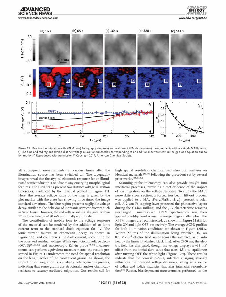


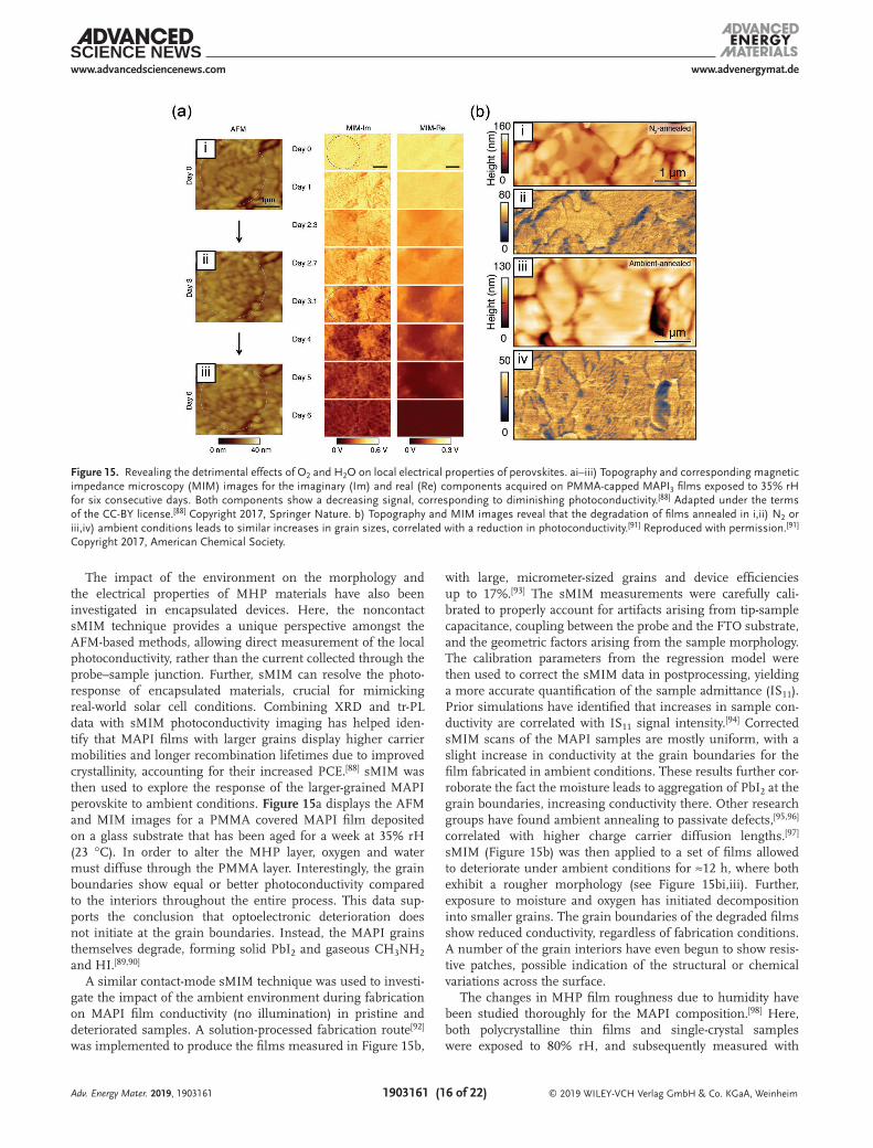


![Modelingof Lead Halide Perovskites for Photovoltaic ... · arXiv:1405.1706v2 [cond-mat.mtrl-sci] 21 May 2014 Modelingof Lead Halide Perovskites for Photovoltaic Applications Radi](https://static.documents.pub/doc/80x56/5eabaa512754357de30f537e/modelingof-lead-halide-perovskites-for-photovoltaic-arxiv14051706v2-cond-matmtrl-sci.jpg)


![Electro‐Optic Modulation in Hybrid Metal Halide Perovskites · nonlinear crystals relies on costly and complicated bonding or deposition processes (heterogeneous integration).[4,5]](https://static.documents.pub/doc/80x56/5f3860b78cb5b531b06e28f0/electroaoptic-modulation-in-hybrid-metal-halide-perovskites-nonlinear-crystals.jpg)


