Page 1
IMAGING SPECTROSCOPY OF HETEROGENEOUS TWO-DIMENSIONAL MATERIALS
A Dissertation
Presented to the Faculty of the Graduate School
of Cornell University
In Partial Fulfillment of the Requirements for the Degree of
Doctor of Philosophy
by
Robin Havener
August 2014
Page 2
This work is licensed under the Creative Commons Attribution-NonCommercial-ShareAlike 4.0
International License. To view a copy of this license, visit
http://creativecommons.org/licenses/by-nc-sa/4.0/.
2014, Robin Havener
Page 3
IMAGING SPECTROSCOPY OF HETEROGENEOUS TWO-DIMENSIONAL MATERIALS
Robin Havener, Ph. D.
Cornell University 2014
Heterogeneities in two-dimensional (2D) materials, including variations in layer number and
stacking order, spatial variations in chemical composition, and point defects, may provide these
systems with a variety of unique optical and electronic properties. Many of these structures form
inherently when 2D materials are produced on a large scale with chemical vapor deposition
(CVD), and artificial heterojunctions between different 2D materials can also be produced by
design. In this work, we address the challenges of visualizing the local structure and composition
of heterogeneous 2D materials, and of establishing clear relationships between these structural
features and the materials’ properties.
For this purpose, we first introduce two novel optical imaging spectroscopy techniques:
DUV-Vis-NIR hyperspectral microscopy and widefield Raman imaging. These techniques
enable comprehensive, all-optical mapping of chemical composition in lateral 2D
heterojunctions, graphene visualization on arbitrary substrates, large-scale studies of defect
distribution in CVD-grown samples, and real-time imaging of dynamic processes. They can also
determine the optical response of an unknown 2D material, and in combination with existing
high resolution imaging tools such as dark-field transmission electron microscopy, they can be
used to establish quantitative structure-property relationships for a variety of 2D heterostructures.
Page 4
We next apply these methods to the first comprehensive study of the optical properties of
twisted bilayer graphene (tBLG), a heterostructure where two graphene layers are rotated by a
relative angle (θ), relating the optical conductivity and Raman spectra to θ for many tBLG
samples. Our results establish the importance of interlayer coupling in tBLG at all θ, and our data
suggest that unique many-body effects play vital roles in both the optical absorption and Raman
response of tBLG. These findings provide a framework for understanding the effects of the θ
degree of freedom in other stacked 2D materials, and the suite of techniques that we have
developed will play a key role in the characterization of heterogeneous 2D materials for years to
come.
Page 5
i
BIOGRAPHICAL SKETCH
Robin W. Havener was born in 1986 and grew up in a small town near Boston, Massachusetts.
She graduated from The Governor’s Academy (formerly Governor Dummer Academy) of
Byfield, Massachusetts in 2004, and studied Materials Science and Engineering at the University
of Pennsylvania in Philadelphia, Pennsylvania. After receiving her B.S.E. in 2008, she entered
the Applied Physics doctoral program at Cornell University in Ithaca, New York. She completed
her Ph.D. research under the supervision of Prof. Jiwoong Park, receiving a National Science
Foundation Graduate Research Fellowship in 2009. Robin will join the technical staff of MIT
Lincoln Laboratory in September of 2014.
Page 7
iii
ACKNOWLEDGMENTS
None of the work that I accomplished during my six years at Cornell would have been possible
without the support (both academic and personal) that I’ve received from a great number of
colleagues, friends, and family throughout my time here. First, I would like to thank to my
parents – while they worked hard from the time I was young to ensure that I’d have the best
possible education, I don’t think they could have guessed that they’d see me through 23 years of
school! Mom and Dad, your advice and encouragement (and fond memories of many trips to the
Boston Museum of Science) have been invaluable. It goes without saying that none of my
achievements so far would have been possible without you, and so I dedicate my dissertation to
you with love.
Next, I’d like to thank my Aunt June, and remember my Uncle Charlie, for showing me
the joy that comes alongside a lifelong passion for learning. Aunt June, a biology teacher, has an
infectious enthusiasm for the outdoors, and every excursion we’ve taken together has been an
adventure, even the ones that haven’t involved wrangling cows. Uncle Charlie, an electrical
engineer, was a voracious reader about all areas of science and beyond, and was always eager to
talk about what he had learned from his most recent book. I’m very grateful to both of you for
your wholehearted support of my decisions to pursue increasingly higher levels of education, and
I’m proud to have followed in both of your footsteps (quite literally for Uncle Charlie’s case,
since he was here at Cornell 50 years ago).
So much of the graduate school experience hinges on picking the right research advisor,
and (very much in hindsight, of course) I consider joining Jiwoong Park’s group to be one of the
best decisions I could have made. Jiwoong, while I often get lost in the details of a project, I
appreciate that I have always been able to rely on you for your scientific insights and your
Page 8
iv
grounded perspective. Jiwoong also never lets any of his students settle for the result that we
have, whether it be a piece of data or a draft of a paper (or thesis), when he knows that we can do
a better job. Even though his attitude has made me want to pull my hair out more than once, I’ve
always had to admit that my work has been better for it.
Another reason I’m glad to have joined Jiwoong’s group is the unusual amount of
collaboration that he fosters between his students. I’m very grateful for the support I’ve received
from all of my labmates, and am fortunate for the opportunity to have contributed to so many
exciting projects during my time in the group. Sang-Yong, I truly value the time and
consideration that you put into mentoring me during my first year and a half – you went above
and beyond, and gave me a great foundation for my research. Lola and Cheol-Joo, thank you for
tirelessly growing the beautiful samples featured in this dissertation. Matt and Fai, thank you for
making the basement of PSB a little less lonely with candy and lots of optics advice. Dan, thank
you for showing me what it means to work hard, and thanks as well to Li and Mike for your help
with nanotubes during the early years. Lulu, Wei, and Mark (and Cheol-Joo and Lola, again),
thank you for taking the time to advise me on how to fabricate my own devices, something I put
off doing for far too long. Carlos, Michal, Zenghui, and Joel, thank you for all of your additional
contributions to my published research. Kan-Heng, Saien, Yimo, Yui, and Kibum, I’m so glad
that we’ve been able to work together, and I’m already excited to see what you’ve accomplished
during your short time here.
Next, I owe a special thanks to my theorist collaborators – Yufeng Liang and Li Yang
from Washington University in St. Louis, and Houlong Zhuang and Richard Hennig from
Cornell. The discussions we had were invaluable during the time that we were struggling to
disentangle the optical properties of twisted bilayer graphene, and I would have been lost without
Page 9
v
your insights. I’d also like to thank Paul McEuen for his intellectual and career-related support,
and Josh Kevek for his help building the Kavli DUV microscope. In addition, I’ve enjoyed a
number of collaborations and fun scientific discussions with several members of David Muller’s
group, Robby, Megan, Elliot, and Julia, and I very much appreciate the support of my special
committee, Poul Petersen and Dan Ralph.
Finally, I’ve been incredibly fortunate that many of my classmates and labmates at
Cornell have also become some of my dearest friends. Lola, Mark, Carlos, Cheol-Joo, Julia,
Robby, and of course, Wei, I can’t imagine anyone else with whom I’d rather celebrate and
commiserate the ups and downs of graduate school. You made Ithaca my home during the time
we were here together, and it was thanks to all of you that this whole experience was actually
(mostly) fun. It is unfortunate that graduating means that many of us will move away from each
other, but I’m excited to find out where the next stage of our lives will take us.
Page 10
vi
TABLE OF CONTENTS
Chapter 1 : INTRODUCTION........................................................................................................ 1
1.1 | Overview ............................................................................................................................. 1
1.2 | Various 2D materials ........................................................................................................... 4
1.3 | Methods of producing 2D materials .................................................................................... 7
1.4 | Structure of CVD-grown 2D materials ............................................................................... 9
1.5 | Lateral Patterning .............................................................................................................. 11
1.6 | Transfer .............................................................................................................................. 13
1.7 | Outlook .............................................................................................................................. 14
References ................................................................................................................................. 17
Chapter 2 : IMAGING TWO-DIMENSIONAL MATERIALS ................................................... 21
2.1 | Introduction ....................................................................................................................... 21
2.2 | Electron microscopy .......................................................................................................... 22
2.3 | Scanning probe microscopy .............................................................................................. 26
2.4 | Optical microscopy ............................................................................................................ 29
2.5 | Outlook .............................................................................................................................. 31
References ................................................................................................................................. 34
Chapter 3 : DUV-VIS-NIR HYPERSPECTRAL IMAGING ...................................................... 36
3.1 | Introduction ....................................................................................................................... 36
3.2 | Absorption spectroscopy ................................................................................................... 37
3.3 | Details of the DUV-Vis-NIR microscope.......................................................................... 40
3.4 | Monochromatic and hyperspectral imaging ...................................................................... 44
3.5 | Quantitative absorption spectroscopy................................................................................ 46
3.6 | Imaging on silicon substrates ............................................................................................ 50
3.7 | Conclusion ......................................................................................................................... 51
Page 11
vii
References ................................................................................................................................. 52
Chapter 4 : WIDEFIELD RAMAN IMAGING ........................................................................... 54
4.1 | Introduction ....................................................................................................................... 54
4.2 | Raman spectroscopy .......................................................................................................... 55
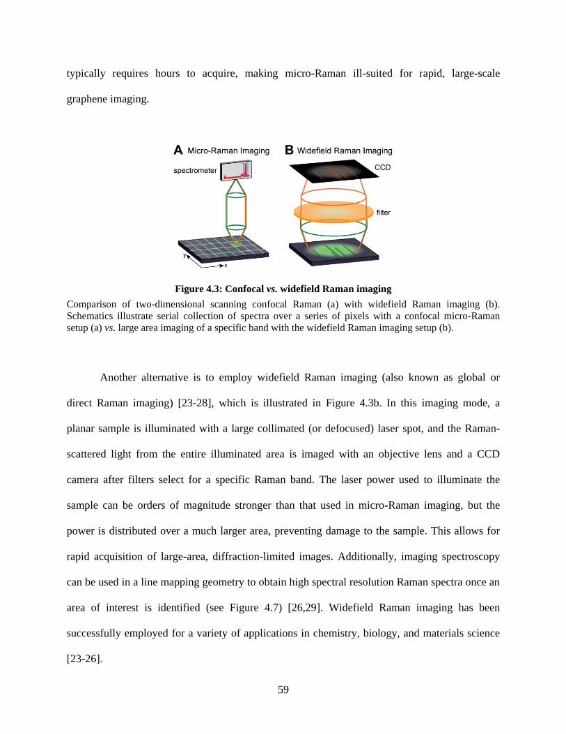
4.3 | Widefield and confocal microscopy .................................................................................. 58
4.4 | Widefield Raman microscope design ................................................................................ 60
4.5 | Spectrally resolved imaging .............................................................................................. 63
4.6 | Thermal effects of laser power .......................................................................................... 66
4.7 | Substrate-independent imaging ......................................................................................... 67
4.8 | Defect mapping ................................................................................................................. 70
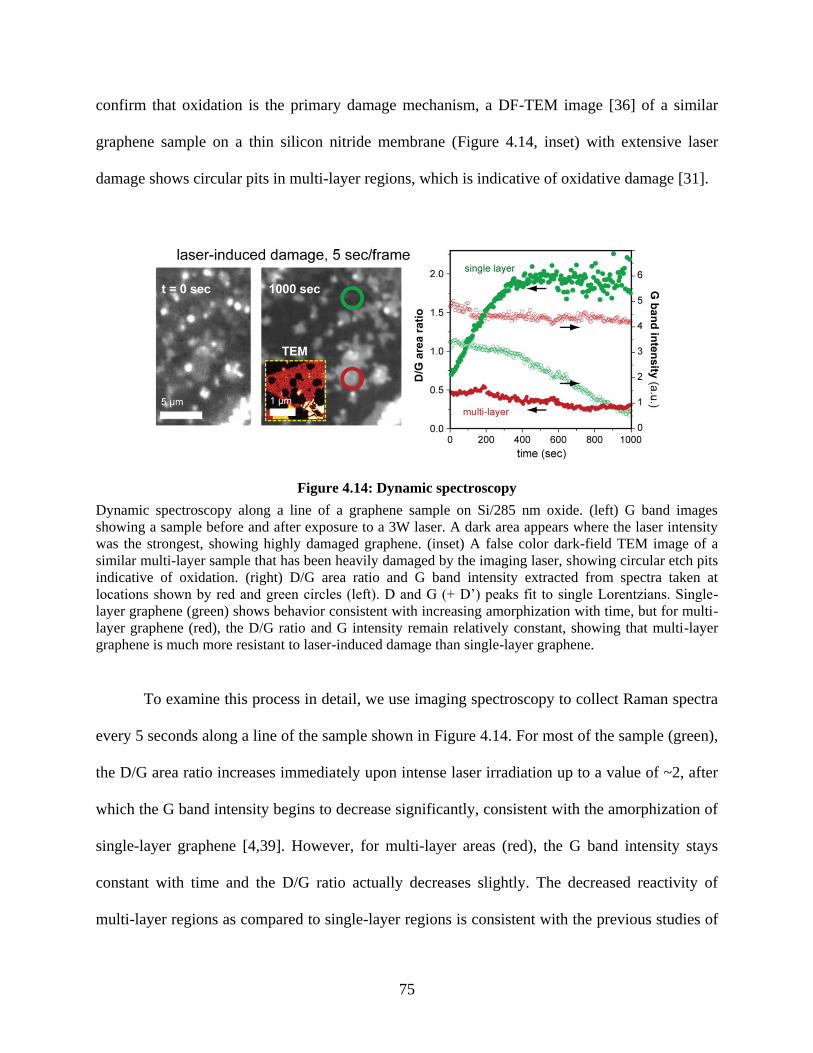
4.9 | Dynamic imaging and spectroscopy .................................................................................. 73
4.10 | Conclusion ....................................................................................................................... 76
References ................................................................................................................................. 77
Chapter 5 : BAND STRUCTURE AND OPTICAL ABSORPTION OF TWISTED BILAYER
GRAPHENE ................................................................................................................................. 79
5.1 | Introduction ....................................................................................................................... 79
5.2 | Defining the physical structure of tBLG ........................................................................... 80
5.3 | Electronic properties .......................................................................................................... 85
5.4 | Calculated optical properties of tBLG ............................................................................... 89
5.5 | Experimental results .......................................................................................................... 97
5.6 | Applications ..................................................................................................................... 101
5.7 | Conclusion ....................................................................................................................... 103
References ............................................................................................................................... 105
Chapter 6 : MANY-BODY OPTICAL PROCESSES IN TWISTED BILAYER GRAPHENE 107
6.1 | Introduction ..................................................................................................................... 107
Page 12
viii
6.2 | Tight binding description of tBLG optical absorption vs. experiment ............................ 109
6.3 | Excitonic effects .............................................................................................................. 111
6.4 | Bound excitons in tBLG .................................................................................................. 118
6.5 | θ-dependence of Raman scattering of tBLG ................................................................... 119
6.6 | Mechanism for G band enhancement .............................................................................. 126
6.7 | Applications ..................................................................................................................... 130
6.8 | Conclusion ....................................................................................................................... 133
References ............................................................................................................................... 134
Chapter 7 : FUTURE DIRECTIONS ......................................................................................... 136
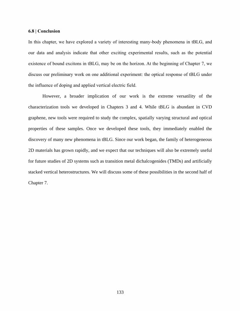
7.1 | Introduction ..................................................................................................................... 136
7.2 | Optical properties of tBLG vs. doping and vertical field ................................................ 137
7.3 | MoS2 and related transition metal dichalcogenides ......................................................... 141
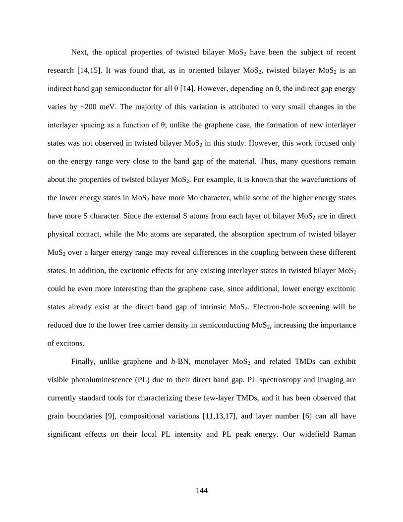
7.4 | Artificial vertical heterostructures ................................................................................... 145
7.5 | Summary ......................................................................................................................... 147
References ............................................................................................................................... 149
Page 13
ix
LIST OF FIGURES
Figure 1.1: Typical thin films vs. 2D materials .............................................................................. 2
Figure 1.2: Graphene and hexagonal boron nitride ........................................................................ 5
Figure 1.3: Molybdenum disulfide ................................................................................................. 6
Figure 1.4: Heterogeneities in CVD graphene ................................................................................ 9
Figure 1.5: Lateral stitching and patterned regrowth .................................................................... 12
Figure 1.6: CVD graphene transfer ............................................................................................... 13
Figure 2.1: STEM and EELS imaging of 2D materials ................................................................ 22
Figure 2.2: Dark-field TEM imaging of graphene ........................................................................ 24
Figure 2.3: SEM of graphene ........................................................................................................ 25
Figure 2.4: AFM of graphene ....................................................................................................... 27
Figure 2.5: STM of graphene ........................................................................................................ 28
Figure 2.6: Making graphene visible ............................................................................................ 29
Figure 3.1: Optical absorption in graphene................................................................................... 38
Figure 3.2: UV absorption spectra of graphene and h-BN ........................................................... 39
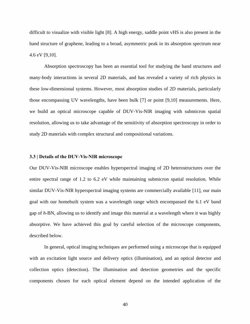
Figure 3.3: Schematic and photographs of DUV-Vis-NIR microscope ....................................... 41
Figure 3.4: Reflective objective .................................................................................................... 43
Figure 3.5: Sample illumination and image normalization ........................................................... 43
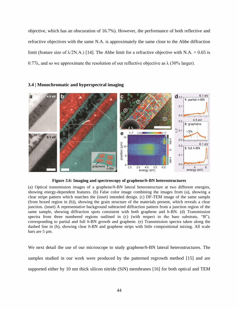
Figure 3.6: Imaging and spectroscopy of graphene/h-BN heterostructures ................................. 44
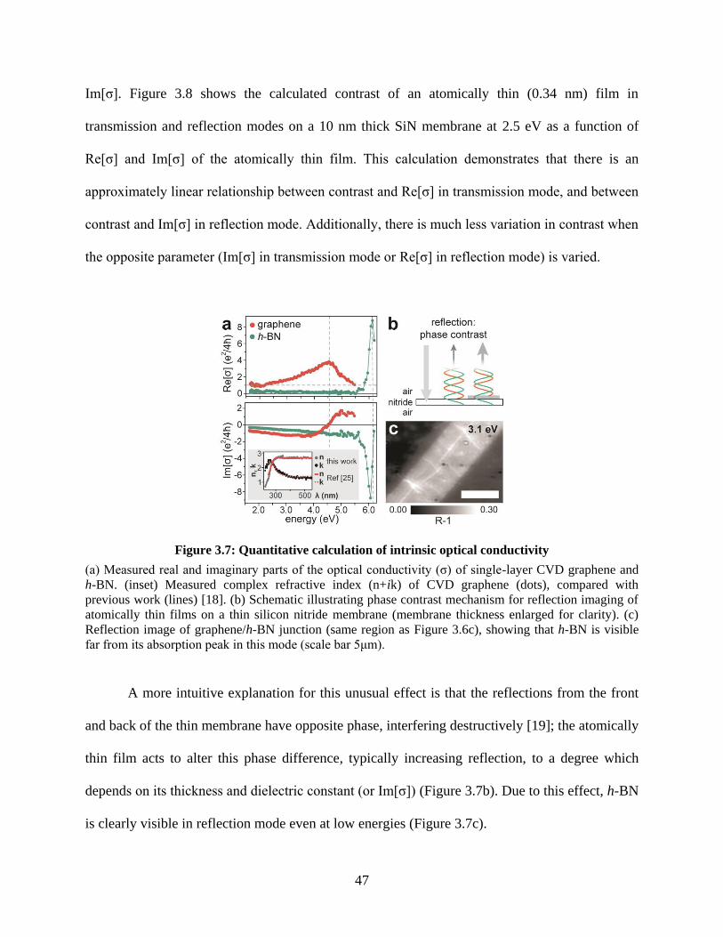
Figure 3.7: Quantitative calculation of intrinsic optical conductivity .......................................... 47
Figure 3.8: Contrast as a function of Re[σ] and Im[σ] ................................................................. 48
Figure 3.9: Reflection spectroscopy on Si/SiO2 ........................................................................... 50
Figure 4.1: Raman spectrum of graphene ..................................................................................... 56
Page 14
x
Figure 4.2: Raman processes in graphene..................................................................................... 57
Figure 4.3: Confocal vs. widefield Raman imaging ..................................................................... 59
Figure 4.4: Schematic of widefield Raman setup ......................................................................... 61
Figure 4.5: Rapid Raman imaging of sp2-bonded carbon materials ............................................. 62
Figure 4.6: Tunable bandpass filter .............................................................................................. 63
Figure 4.7: Spectrally resolved imaging ....................................................................................... 64
Figure 4.8: Graphene temperature vs. laser power ....................................................................... 66
Figure 4.9: Substrate-independent imaging .................................................................................. 67
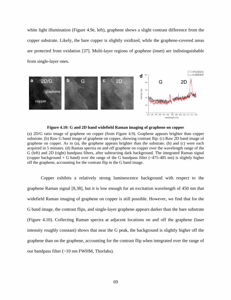
Figure 4.10: G and 2D band widefield Raman imaging of graphene on copper .......................... 69
Figure 4.11: D band imaging of CVD graphene ........................................................................... 70
Figure 4.12: Raman and DF-TEM grain boundary imaging ......................................................... 72
Figure 4.13: Time-resolved Raman imaging ................................................................................ 73
Figure 4.14: Dynamic spectroscopy ............................................................................................. 75
Figure 5.1: Single layer, Bernal, and twisted bilayer graphene .................................................... 80
Figure 5.2: Commensurate tBLG .................................................................................................. 82
Figure 5.3: Unit cell size vs. θ ....................................................................................................... 83
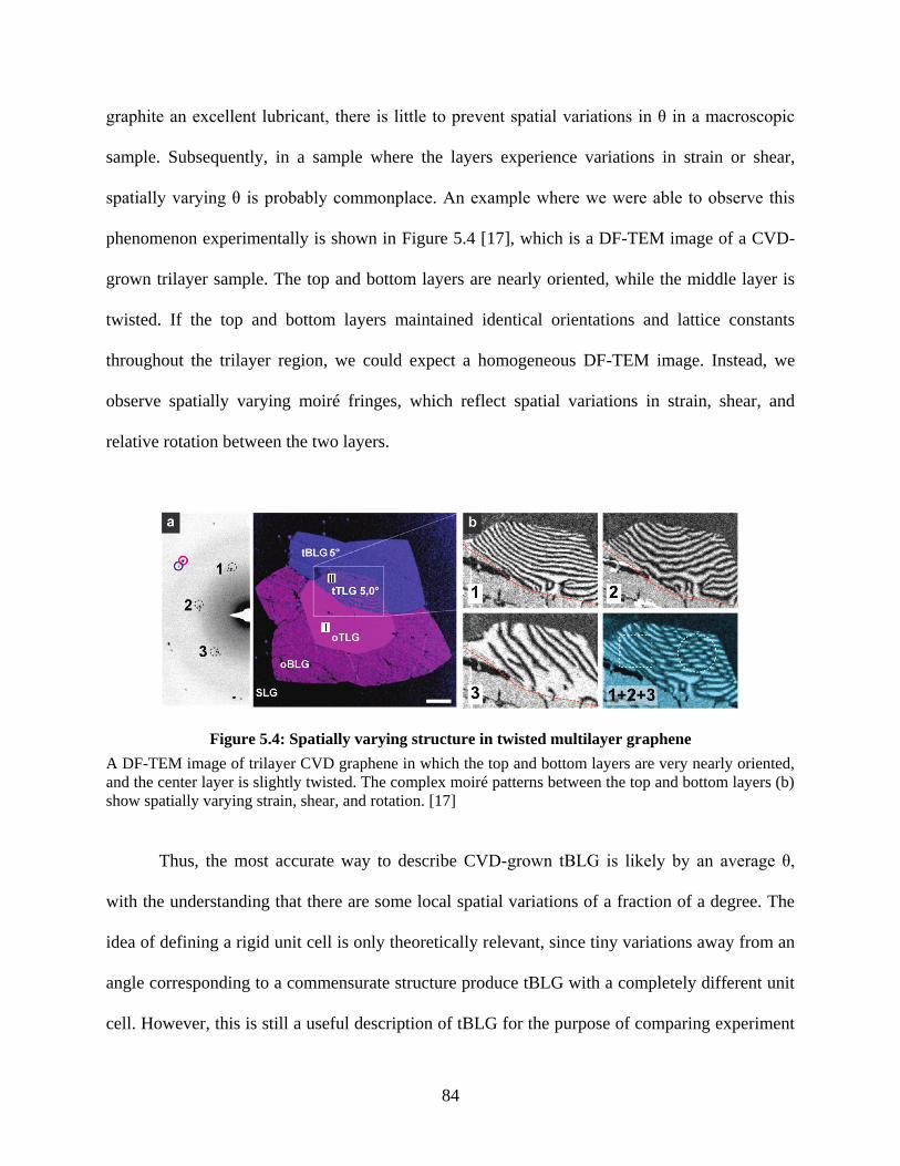
Figure 5.4: Spatially varying structure in twisted multilayer graphene ........................................ 84
Figure 5.5: Continuum model of tBLG band structure ................................................................. 85
Figure 5.6: Experimental studies of the tBLG DOS ..................................................................... 87
Figure 5.7: Full band structure of graphene .................................................................................. 88
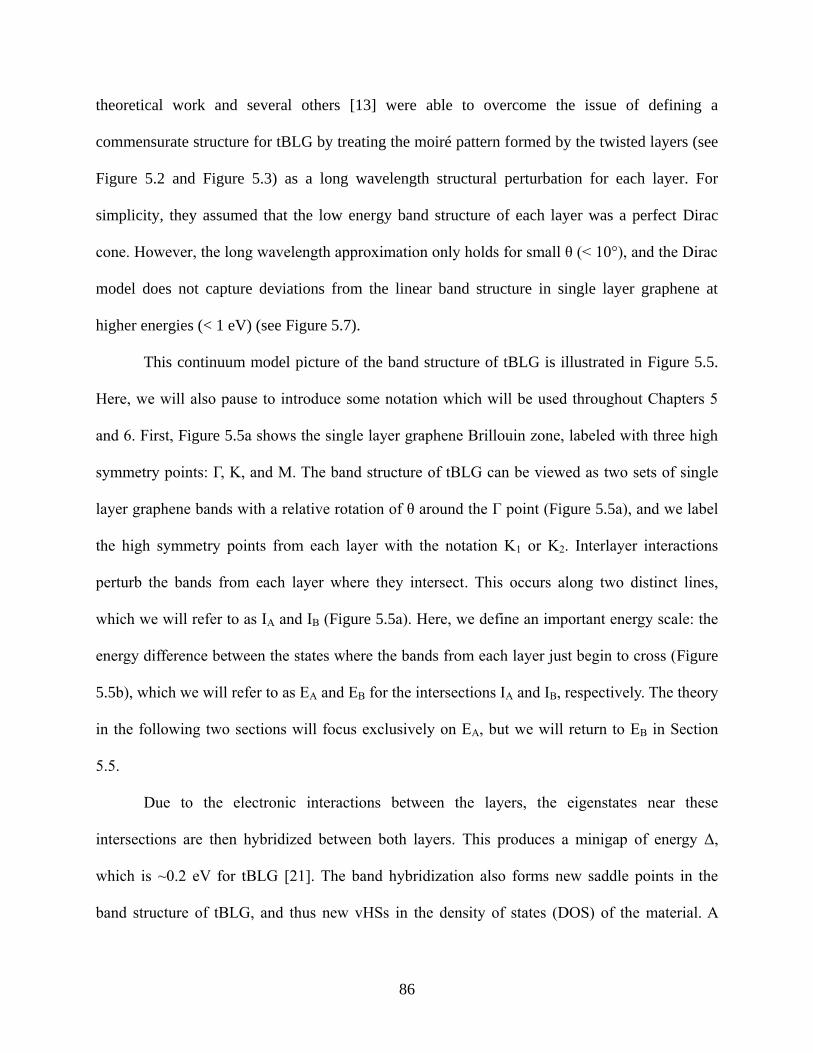
Figure 5.8: JDOS in tBLG ............................................................................................................ 90
Figure 5.9: Calculated JDOS with coupling ................................................................................. 92
Figure 5.10: Tight binding band structure of 13.2° tBLG ............................................................ 93
Page 15
xi
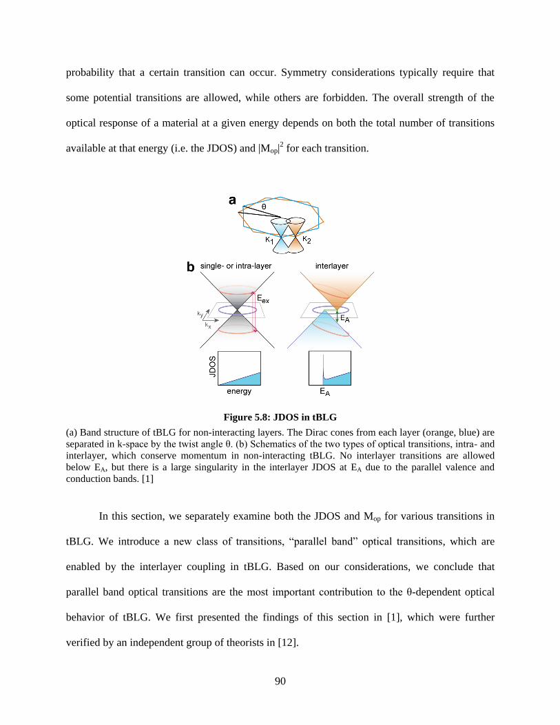
Figure 5.11: Optical matrix element ............................................................................................. 95
Figure 5.12: Calculated optical absorption of tBLG ..................................................................... 96
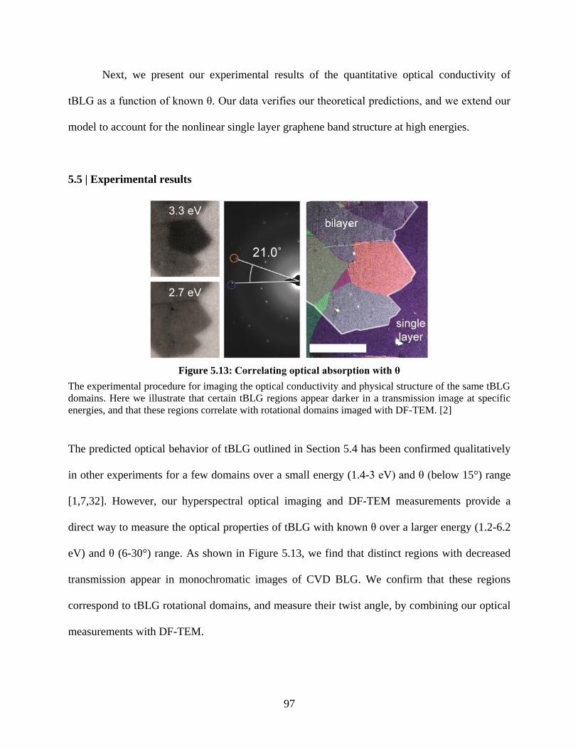
Figure 5.13: Correlating optical absorption with θ ....................................................................... 97
Figure 5.14: Optical conductivity of tBLG ................................................................................... 98
Figure 5.15: 2D plot of tBLG optical conductivity....................................................................... 99
Figure 5.16: All-optical θ mapping ............................................................................................. 101
Figure 5.17: tBLG imaging on Si/SiO2 ....................................................................................... 102
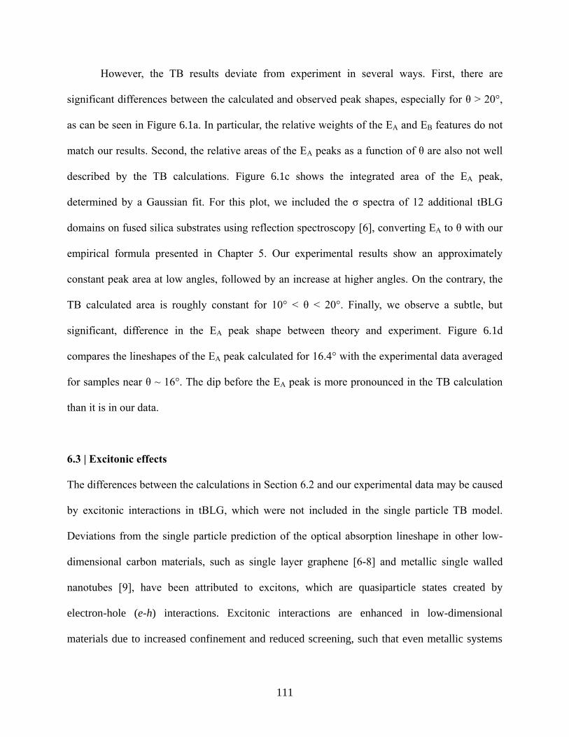
Figure 6.1: Comparison of experimental data with tight binding calculations ........................... 109
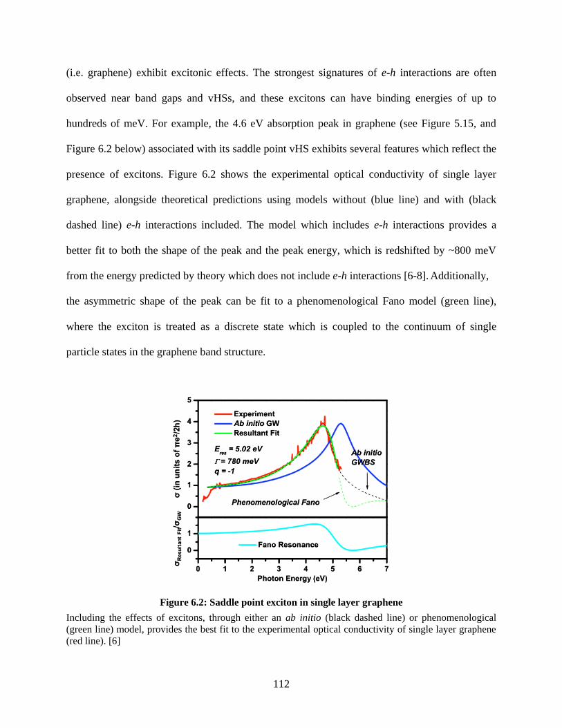
Figure 6.2: Saddle point exciton in single layer graphene .......................................................... 112
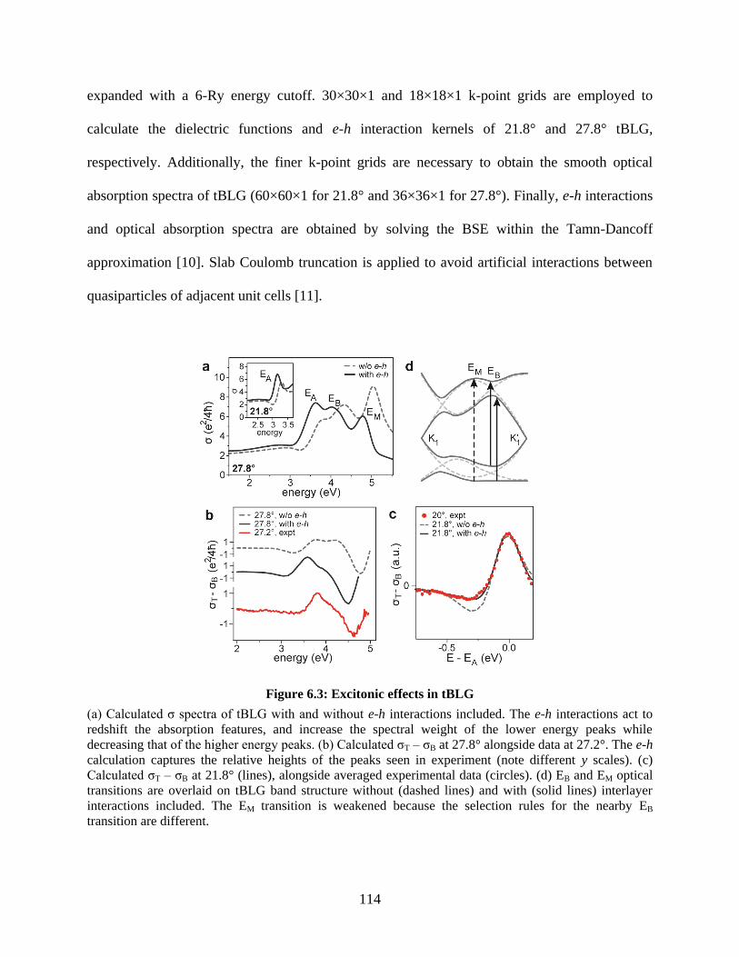
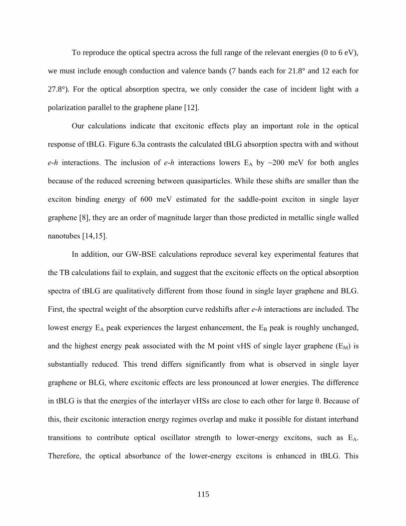
Figure 6.3: Excitonic effects in tBLG ......................................................................................... 114
Figure 6.4: Bound excitons in tBLG ........................................................................................... 118
Figure 6.5: Raman imaging of tBLG .......................................................................................... 121
Figure 6.6: G band enhancement on resonance .......................................................................... 122
Figure 6.7: Excitation energy dependent G band resonance ....................................................... 122
Figure 6.8: G peak position and width dependence on θ ............................................................ 123
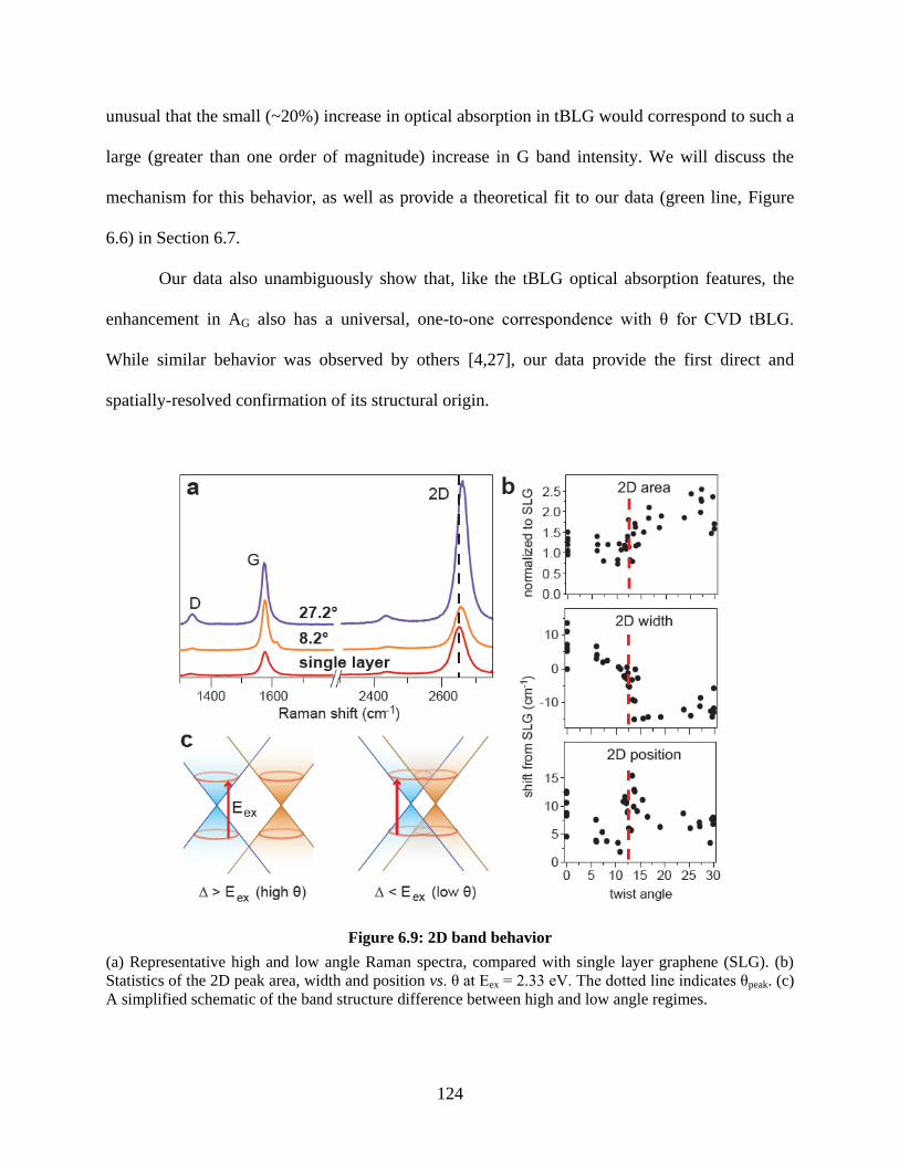
Figure 6.9: 2D band behavior ..................................................................................................... 124
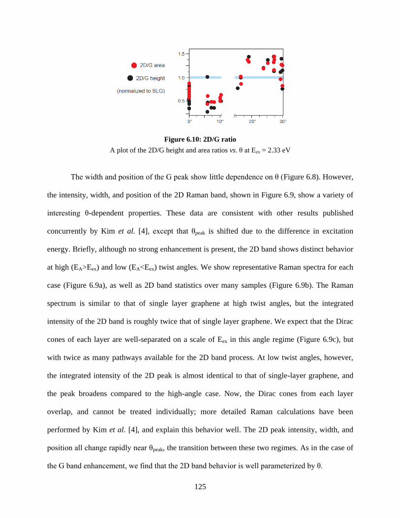
Figure 6.10: 2D/G ratio ............................................................................................................... 125
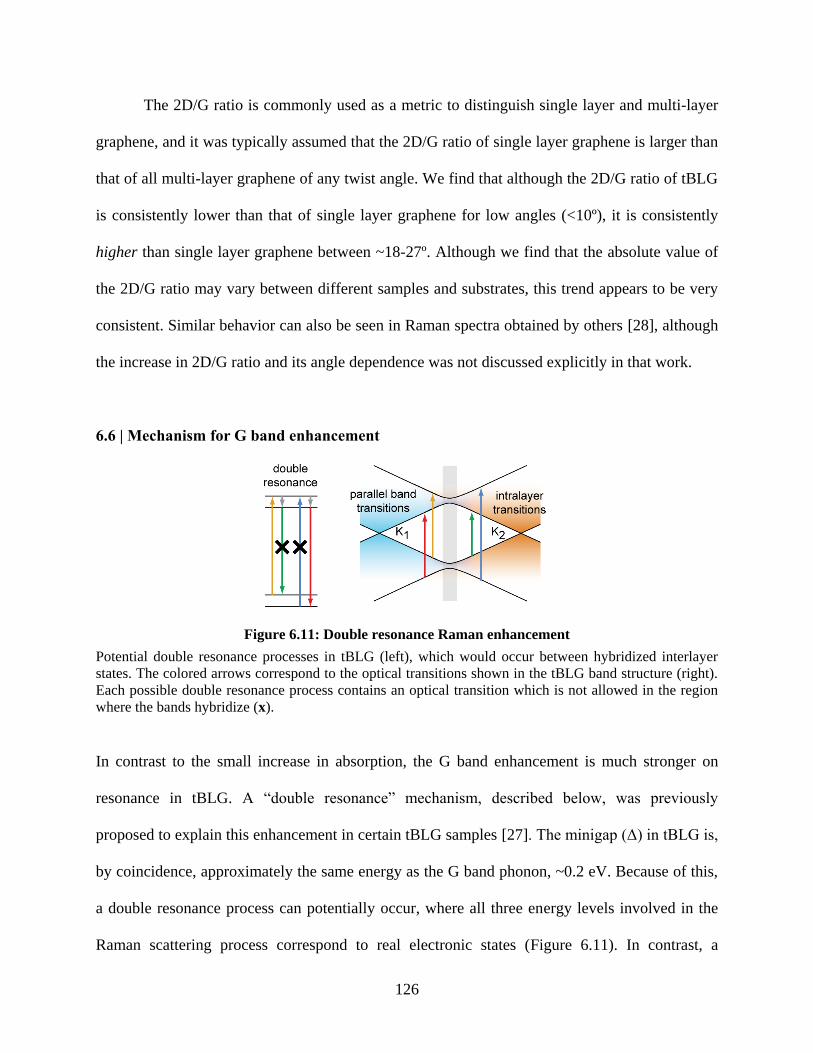
Figure 6.11: Double resonance Raman enhancement ................................................................. 126
Figure 6.12: Simplified calculation of G band intensity ............................................................. 128
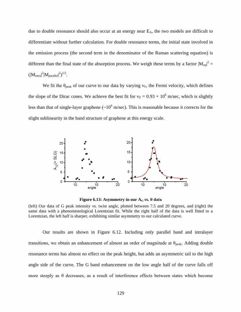
Figure 6.13: Asymmetry in our AG vs. θ data ............................................................................. 129
Figure 6.14: Raman imaging of interlayer coupling in tBLG ..................................................... 131
Figure 6.15: AFM of artificially transferred bilayer graphene ................................................... 132
Figure 7.1: Doping and vertical field in tBLG ............................................................................ 137
Page 16
xii
Figure 7.2: Transparent, dual gated tBLG transistor .................................................................. 138
Figure 7.3: Field and doping effects on the EA peak .................................................................. 140
Figure 7.4: Doping and field dependence of EA peak parameters .............................................. 140
Figure 7.5: Absorption spectra of bulk TMDs ............................................................................ 143
Figure 7.6: Artificial vertical heterostructures ............................................................................ 145
Figure 7.7: Controlling twist angle in vertical stacks ................................................................. 146
Page 17
1
Chapter 1 : INTRODUCTION
1.1 | Overview
Developing precise control over the composition and properties of thin films has been crucial for
many advances in modern technology. The manufacture of products such as computer chips,
light emitting diodes, and semiconductor lasers relies heavily on thin film deposition and
patterning techniques to transform a solid substrate into a complex, functional device. However,
while the active areas of these devices can be as thin as a few atoms, they are permanently
affixed to their bulk substrates. These substrates often serve little purpose beyond that of
mechanical support, limiting many potential thin film device geometries.
Two-dimensional (2D) materials are an emerging class of thin films which do not require
a supporting substrate, and which have created significant interest for both fundamental research
and device applications. 2D materials are mechanically continuous sheets which are a few atoms
or fewer in thickness. What makes these thin films unique is that they are self-contained: in-
plane, they are held together with strong covalent bonds, but they lack the reactive dangling
bonds which are found at most other solid surfaces. Unlike many other thin films, they are
typically stable if removed from a supporting substrate. In addition, if a 2D material is placed on
top of a bulk surface or another 2D material, it interacts through weak van der Waals forces
which do not disrupt its in-plane bonding.
An analogy which provides an excellent summary of these properties, and indicates their
exciting potential, is that 2D materials can act as discrete, atomically thin “building blocks.” The
implication is that some of the most fascinating aspects of these thin films are the ways in which
they can be manipulated and combined to form complex structures. One possibility, like other
Page 18
2
thin films, is that 2D materials with different chemical compositions may be deposited layer by
layer to form a device. There are currently many known 2D materials with a variety of optical
and electronic properties. The most familiar example is graphene, a semimetallic, single atom
thick sheet of carbon atoms, which will be the main focus of this dissertation. However, other 2D
materials, such as insulating hexagonal boron nitride (h-BN) and semiconducting molybdenum
disulfide (MoS2), have been studied intensively during the past several years, and more exotic
examples continue to be discovered. As with other thin films, it is possible to synthesize many of
these materials on a wafer scale, and exert a high degree of control over their properties by
varying parameters such as their composition, physical structure, or dopant density.
Figure 1.1: Typical thin films vs. 2D materials
(left) MBE can be used to produce highly crystalline thin films and exert precise control over the
composition of each atomic layer, but these films are covalently bonded to their bulk substrate. (right) 2D
materials exist independently of a supporting substrate. Since the bonding between layers is weaker, their
interlayer rotation (θ) is a new degree of freedom. It is also possible to pattern lateral heterostructures
between 2D materials with different compositions.
However, there are also a number of novel 2D device geometries which cannot be
produced with other thin films. First, because 2D materials are self-contained, they can be
manipulated, processed, and patterned easily, often with few alterations to their intrinsic
Page 19
3
properties. They can also be transferred to arbitrary substrates for a variety of applications, and
can conform to irregular or flexible surfaces due to their extreme thinness.
In addition, many of the structural features which are formed when various 2D materials
are combined are unique to this class of thin films (Figure 1.1). For example, unlike epitaxial
films (such as those produced with molecular beam epitaxy) which require registry between the
crystal lattices of each adjacent layer, stacked 2D materials can form atomically precise vertical
junctions regardless of their intrinsic lattice parameters. Moreover, the stacking of weakly
coupled, crystalline 2D layers adds a unique degree of freedom, the relative rotation angle (θ)
between the orientations of each layer. A number of novel, θ-dependent optical and electronic
signatures have recently been observed in multilayers of 2D materials such as graphene and
MoS2, providing additional tunability to the properties of these systems. 2D materials with
different compositions or dopant densities can also be stitched together to make mechanically
continuous, atomically thin lateral heterostructures, aided by the ability to pattern and process
them.
While the intrinsic properties of 2D materials such as graphene, MoS2, and h-BN have
been thoroughly characterized over the past decade, many of the properties of the novel,
heterogeneous 2D systems described above have remained poorly understood. This dissertation
addresses two challenges in this area. First, new tools are required for the basic characterization
of these systems. Because the composition and structure of 2D materials can vary spatially,
imaging, rather than point or bulk measurements, is crucial for their characterization. However,
in addition to being sensitive to variations in these materials’ composition and structure, ideal
imaging techniques should also operate independently of the substrate to which the 2D material
is transferred. Moreover, a single tool should be able to identify and characterize many different
Page 20
4
2D materials in a single heterostructure device simultaneously. In Chapters 3 and 4, we introduce
two novel optical tools for imaging spectroscopy which are optimized for rapid, large scale
characterization of 2D materials on a variety of substrates.
Second, we begin to explore the ways in which these complex features can affect the
properties of the resulting 2D materials. Taking advantage of the unique capabilities of the tools
developed in the preceding chapters, we focus on quantitatively characterizing the effects of
interlayer rotation (θ) on the optical properties of a prototypical stacked 2D material, twisted
bilayer graphene (tBLG). Our work represents the first comprehensive study of the θ-dependent
structure-property relationships in any stacked 2D system. In Chapters 5 and 6, we consider the
relationship between θ and the band structure and optical transitions in tBLG, as well as the
many-body optical processes in this material, including excitonic effects and Raman scattering.
In this chapter, we will review the current state of 2D materials synthesis, heterojunction
fabrication, and transfer to arbitrary substrates, focusing on graphene and other 2D materials
produced on a large scale with chemical vapor deposition (CVD). As we will discuss, CVD-
grown 2D materials are excellent model systems for studying twisted multilayers, and serve as
starting points for lateral patterning and transfer.
1.2 | Various 2D materials
The family of two-dimensional materials continues to grow, and several examples are presented
in Figure 1.2 and Figure 1.3. Graphene, the best known 2D material and the subject of the 2010
Nobel Prize in Physics [1], is a semimetallic, single-atom thick sheet of carbon atoms arranged in
a honeycomb lattice. Hexagonal boron nitride (h-BN) is an analog to graphene whose carbon
atoms are replaced by alternating boron and nitrogen atoms. It is an insulator with a large optical
Page 21
5
band gap of ~6 eV [2,3]. Also of note, although not the main focus of this work, are monolayer
transition metal dichalcogenides (TMDs). TMDs are three atoms thick, and have the chemical
composition MX2, where M is a metal atom (examples include Mo, W, Cr, Co, Ni, and Ta) and X
is a chalcogen from group 16 of the periodic table (S, Se, Te) [4,5]. These materials can exhibit a
variety of electronic properties [6], but many of the most studied examples (e.g. MoS2, MoSe2,
WS2) are semiconductors.
Figure 1.2: Graphene and hexagonal boron nitride
(a, top) An artist’s rendition of a freestanding sheet of single layer graphene. Carbon atoms are bonded in
a hexagonal lattice which is one atom thick. [7] (bottom) The tight binding calculated band structure of
graphene, highlighting the linear, gapless bands at low energies. Here, energy is plotted in units of a tight
binding parameter t = 2.7 eV. [8] (b, top) The structure of hexagonal boron nitride (h-BN) which is
similar to that of graphene, except that it contains alternating atoms of boron (blue) and nitrogen (orange).
[9] (bottom) The ab initio calculated band structure of monolayer h-BN, illustrating the large band gap.
[10]
Early studies of 2D materials focused on the fundamental physics of pristine single- and
few-layer samples. While some of these findings will be discussed in more detail in subsequent
Page 22
6
chapters, we summarize several main results here. First, monolayer graphene has a unique linear
band structure near its charge neutrality point, and has served as a platform for many studies of
two-dimensional physics, including the integer [11,12] and fractional [13,14] quantum Hall
effects. Pristine graphene exhibits very high carrier mobility [15], as well as high mechanical
strength [16] and uniform broadband optical absorption [17]. Bernal stacked (i.e. oriented)
bilayer graphene is also metallic, but a band gap can be opened in this material under the
application of a vertical electric field [18].
Figure 1.3: Molybdenum disulfide
(a) A top-down (left) and side (right) view of MoS2, a TMD. MoS2 is three atoms thick, but has a similar
symmetry as h-BN when viewed from the top. [19,20] (b) The ab initio calculated band structures of
monolayer and bilayer MoS2, showing the transition from a direct to an indirect band gap. [21]
Next, for MoS2 and several other semiconducting TMDs, it was found that monolayers
have a direct band gap, while oriented multilayers have an indirect band gap [22]. The additional
valley degree of freedom in MoS2, coupled with the direct band gap of MoS2 monolayers, has led
Page 23
7
to a variety of interesting optical physics in this material and other related TMDs (such as MoSe2
and WS2) [23,24]. Lastly, insulating h-BN has been shown to be a high quality dielectric for
graphene [3] and other 2D electronic devices, reducing spatial fluctuations in the charge density
of the active material due to its lack of dangling bonds.
In order to perform these fundamental studies, it was essential to develop methods of
isolating 2D materials. The initial studies of the intrinsic properties of the 2D materials discussed
in this section were performed on high quality samples, which were produced on a small scale
using a mechanical exfoliation technique. Later, methods were developed to synthesize 2D
materials on a larger scale, toward the goal of harnessing some of their unique properties for real
world applications. Each of these methods of producing 2D materials will be discussed in more
detail in the following section.
1.3 | Methods of producing 2D materials
The first atomically thin 2D crystals, including graphene and MoS2, were isolated in 2004. These
initial studies used mechanical exfoliation from high quality bulk crystals, or the “Scotch tape
method” [25,26], to isolate single- and few-layer 2D samples. After mechanical exfoliation is
performed, the target substrate is covered in pieces of the material which vary randomly in size
and number of layers. The user must search the entire substrate by eye with an optical
microscope to locate the thinnest pieces, which are typically several microns in extent. While
exfoliation continues to produce the highest quality 2D crystals, this technique cannot create
large area samples.
However, for any viable technological application, it is necessary to produce 2D
materials on a large scale. For the case of graphene, it has been known for several decades that
Page 24
8
thin graphitic layers can form easily on many metal surfaces, but they were once considered
impurities [27]. After graphene was isolated by mechanical exfoliation, it was found that more
controlled, few-layer islands of graphene can grow epitaxially under ultrahigh vacuum on certain
metal substrates [28-30]. Graphene can also grow epitaxially on silicon carbide, providing large
area samples with various numbers of layers [31,32]. With all of these growth methods, however,
the graphene is difficult to remove from its substrate. In many cases, there is also strong
electronic coupling between the graphene and the substrate, which can alter the intrinsic
properties of the graphene.
Chemical vapor deposition (CVD), adopted in 2009 for graphene, is a technique for
synthesizing a variety of single- and few-layer 2D materials of arbitrary size. The CVD process
involves heating a substrate in a furnace and flowing in gaseous precursors, which decompose
and deposit solid material onto the substrate. For the proper choice of substrate and growth
conditions, this process can be self-limiting, and a monolayer of the target material can grow.
Copper was found to be an ideal growth substrate for both graphene [33,34] and h-BN [35-37],
and can produce monolayer films of both materials. Importantly, the 2D material is easily
removed from the substrate after growth (see Section 1.6). The CVD growth of TMDs is not as
well established as that of graphene or h-BN, but current methods enable the production of high
quality MoS2 monolayers on small areas of the growth substrate [38,39].
CVD-grown 2D materials, specifically graphene and h-BN, are the main subjects of this
dissertation. Not only does this growth method produce scalable, high quality samples, but CVD-
grown 2D materials are model systems for studying many of the complex 2D structures
discussed in Section 1.1. Multilayer regions with varying θ often grow during CVD synthesis. In
addition, CVD is easily adapted to introduce compositional variations into the growing material,
Page 25
9
and is necessary to produce laterally patterned samples (Section 1.5). In Section 1.4, we discuss
several common structural features in CVD-grown 2D materials which will be of interest in the
following chapters.
1.4 | Structure of CVD-grown 2D materials
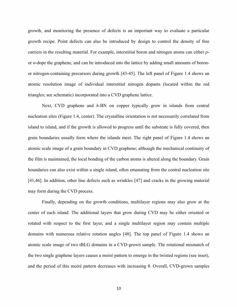
Figure 1.4: Heterogeneities in CVD graphene
The center scanning electron microscope (SEM) image illustrates the typical island growth of CVD
graphene on copper [40], ultimately leading to grain boundaries (STEM image, right) [41] and twisted
multilayers (TEM image, top) [42] in the final material. Point defects (STM image, left) [43] can also be
incorporated into the growth, either unintentionally or by design.
Most CVD growth processes produce inherently heterogeneous 2D films, shown in Figure 1.4.
First, CVD-grown samples can contain localized defects, such as vacancies or substitutional
impurities. When the conditions are not ideal, defects can be introduced unintentionally during
Page 26
10
growth, and monitoring the presence of defects is an important way to evaluate a particular
growth recipe. Point defects can also be introduced by design to control the density of free
carriers in the resulting material. For example, interstitial boron and nitrogen atoms can either p-
or n-dope the graphene, and can be introduced into the lattice by adding small amounts of boron-
or nitrogen-containing precursors during growth [43-45]. The left panel of Figure 1.4 shows an
atomic resolution image of individual interstitial nitrogen dopants (located within the red
triangles; see schematic) incorporated into a CVD graphene lattice.
Next, CVD graphene and h-BN on copper typically grow in islands from central
nucleation sites (Figure 1.4, center). The crystalline orientation is not necessarily correlated from
island to island, and if the growth is allowed to progress until the substrate is fully covered, then
grain boundaries usually form where the islands meet. The right panel of Figure 1.4 shows an
atomic scale image of a grain boundary in CVD graphene; although the mechanical continuity of
the film is maintained, the local bonding of the carbon atoms is altered along the boundary. Grain
boundaries can also exist within a single island, often emanating from the central nucleation site
[41,46]. In addition, other line defects such as wrinkles [47] and cracks in the growing material
may form during the CVD process.
Finally, depending on the growth conditions, multilayer regions may also grow at the
center of each island. The additional layers that grow during CVD may be either oriented or
rotated with respect to the first layer, and a single multilayer region may contain multiple
domains with numerous relative rotation angles [48]. The top panel of Figure 1.4 shows an
atomic scale image of two tBLG domains in a CVD-grown sample. The rotational mismatch of
the two single graphene layers causes a moiré pattern to emerge in the twisted regions (see inset),
and the period of this moiré pattern decreases with increasing θ. Overall, CVD-grown samples
Page 27
11
have enabled the first systematic studies of point defects, grain boundaries, and twisted
multilayers in 2D materials, since exfoliated samples typically originate from pure, highly
crystalline bulk materials in which every layer is oriented.
While these features are interesting subjects of study, we note that it can also be desirable
to reduce heterogeneities in CVD-grown samples in order to carefully control the properties of
the final product. To increase grain size, the nucleation density of graphene can be reduced to as
little as ~1/cm2 [49] by tuning the flow rates of the precursor and carrier gases, as well as the
degree of initial oxidation of the copper surface. Additionally, a crystalline surface, such as (111)
copper [50-52] or (100) germanium [53], can enable preferential alignment of individual
graphene or h-BN islands during growth, producing a crystalline sample despite a higher
nucleation density. Both of these methods have the potential to produce homogeneous 2D
materials on a wafer scale.
1.5 | Lateral Patterning
As discussed previously, the composition and dopant density of CVD-grown 2D materials
depends on the precursor gases used during growth. By extension, it is also possible to laterally
control the composition of a single 2D layer during growth. Lateral variations can be produced
by stopping the growth of the first material before it fully covers the substrate, and then
introducing the precursors for the second material. Different 2D materials can be “stitched”
together to form a mechanically continuous sheet if they have similar structures and lattice
constants, such as intrinsic and doped graphene, graphene and h-BN, or various TMDs. The
graphene/h-BN case has been studied particularly closely, and it has been shown that these
Page 28
12
materials can stitch with atomic precision under certain growth conditions (Figure 1.5a)
[54,56,57].
Figure 1.5: Lateral stitching and patterned regrowth
(a) An atomic resolution STM image of laterally stitched graphene (Gr) and h-BN (BN), illustrating a
continuous, defect-free boundary under ultra-high vacuum growth conditions [54]. (b) An optical image
of graphene (dark) and h-BN (light) regions produced with the patterned regrowth method. (inset) A dark-
field TEM image of a mechanically continuous, suspended graphene/h-BN junction in a similar patterned
sample. Scale bar 250 nm [55].
Introducing a sequence of different precursors into the furnace during CVD growth
produces a random network of heterojunctions, but the ability to controllably pattern the
composition of a layer is crucial for many applications. This is possible through a recently
developed process termed “patterned regrowth” [55]. After a continuous sheet of one material is
grown with CVD, it is removed from the growth furnace, and selected regions are etched away
using standard photolithography techniques. Then, the sample is reintroduced into the furnace,
and a second material is grown in the patterned region only [55,58]. This technique was shown to
produce mechanically continuous patterned sheets of graphene/h-BN with junctions of width <10
nm (Figure 1.5b). Patterned regrowth can also be used to control the dopant density in graphene
films, potentially enabling the fabrication of p-n junctions embedded within a single 2D film.
Page 29
13
1.6 | Transfer
After growth and any applicable patterning, CVD-grown 2D materials must often be removed
from their growth substrates. For this, a polymer layer, such as poly(methyl methacrylate)
(PMMA), can be spin-coated on top of the 2D material/growth substrate. Then, the growth
substrate can be etched away with a wet etchant, leaving the 2D material/polymer film floating
on top of the etchant (Figure 1.6). The polymer film supports the 2D material, and the entire
structure is fairly robust, allowing the graphene to undergo a series of cleaning steps to remove
organic and inorganic residues [59]. Finally, the polymer/2D material membrane can be
“scooped” onto a target substrate. The polymer film is removed with an organic solvent or
annealing, while the 2D material remains behind [41,60,61].
Figure 1.6: CVD graphene transfer
A schematic illustrating the most commonly used procedure for transferring CVD-grown 2D materials to
other substrates. After etching the growth substrate, the floating PMMA/graphene membrane can be
scooped out of solution onto an arbitrary target substrate [62].
Because 2D materials are self-contained, they can be transferred to arbitrary substrates
for various applications, including silicon wafers for facile electronic device fabrication, fused
silica for optical transparency, or polymer sheets for mechanical flexibility. Although device
quality can depend on the substrate used, many of the intrinsic properties of the 2D material (e.g.
its band structure, optical absorption spectrum, and Raman scattering) are maintained after
Page 30
14
transfer [61]. The basic transfer technique has been adapted to transfer exfoliated samples onto
various substrates [3], as well as for meter-scale roll-to-roll transfer of large area graphene [63].
Regardless of the target substrate, transfer cleanliness remains a significant issue, and can
reduce device performance significantly. Residues from the polymer layer or etchant may remain
after transfer, and contaminants may get trapped between the 2D material and the substrate. For
the transfer of CVD-grown materials, efforts have been made to replace the PMMA layer with a
cleaner support, such as a different polymer [64], PDMS stamp [65] or thermal release tape
[63,66], as well as to dry the film before transfer [67] to reduce contaminants.
Finally, we note that sequential transfers of various 2D materials can be used to create
vertical 2D heterostructures where both the composition and relative angle of each layer may be
controlled. Despite the cleanliness issues discussed above, it is possible to obtain atomically
precise contact between each layer. More details on the production and applications of these 2D
stacks will be discussed in Chapter 7.
1.7 | Outlook
As discussed in this chapter, a variety of unique structural features and compositional variations
can exist in 2D materials, particularly those produced by CVD. Some of these features, such as
twisted multilayers in CVD graphene, can be produced at random during growth; others, like
patterned lateral heterojunctions, are created by design. In either case, it is crucial that we
understand the structure and local composition of the 2D material that results after growth and
patterning, and establish clear relationships between these structural features and the material’s
properties. This feedback will aid in the discovery of new functionalities in heterogeneous 2D
Page 31
15
materials, taking full advantage of the novel ways in which 2D materials can be manipulated and
combined.
Toward this goal, we first need to be able to visualize the structural and compositional
heterogeneities in CVD-grown 2D materials. In this chapter (Figures 1.4 and 1.5), we included
several images of various types of defects and heterostructures which can be found in 2D
materials. In Chapter 2, we will review the microscopy techniques used to obtain these images,
including variants of electron, scanning probe, and optical microscopy. However, these existing
techniques have many shortcomings when it comes to characterizing 2D materials produced with
CVD, particularly for imaging large samples with high throughput and for characterizing
samples after transfer to arbitrary substrates. In Chapters 3 and 4, we introduce two optical
microscopy techniques which bridge this characterization gap. Chapter 3 describes a DUV-Vis-
NIR hyperspectral microscope which can be used to image compositional variations in
graphene/h-BN lateral heterostructures on a large scale, for samples which sit on several
different substrates relevant for device fabrication. Chapter 4 describes a widefield Raman
microscope which enables rapid graphene imaging and characterization on arbitrary substrates.
For the most part, the imaging modalities in Chapters 3 and 4 take advantage of the
known optical responses of various 2D materials, such as the absorption spectra of isolated
graphene and h-BN, or the effect of point defects on the Raman spectrum of graphene. However,
we also outline how each technique can be used to obtain the quantitative optical response of an
unknown 2D material. Combined with the other direct imaging techniques outlined in Chapter 2,
we have assembled a powerful suite of tools which can be used to establish new relationships
between the physical structure and optical properties of 2D materials.
Page 32
16
To culminate our new capabilities, we focus in Chapters 5 and 6 on measuring the
quantitative structure-property relationships between the optical response of twisted bilayer
graphene (tBLG) and its relative rotation angle (θ). As outlined previously, the relative rotation
of stacked atomically thin layers is a degree of freedom which is truly unique to 2D materials.
However, due to the previous difficulties in characterizing both the structure and the properties
of a twisted 2D material simultaneously, the effects of θ on even a very simple system like tBLG
were poorly understood. In Chapter 5, we discuss the relationship between the physical
structure of tBLG, its band structure, and its optical absorption spectrum, while in Chapter 6 we
explore the more complex effects of many-body interactions in tBLG, including excitons and
Raman scattering. This work explores a wealth of new physics which is unique to tBLG, and
establishes θ as a crucial parameter to tune the properties of stacked 2D materials.
Finally, we note that while the remainder of this work will focus on the characterization
of a few model examples (large scale graphene transferred to arbitrary substrates, graphene/h-BN
lateral heterostructures, and CVD twisted bilayer graphene), the techniques we outline here are
currently being adapted to study a variety of 2D systems. Examples include the optical properties
of heterogeneous TMDs or the degree of interlayer coupling in artificially stacked vertical
heterostructures. Similarly, the theoretical framework we develop for the band structure and
optical properties of tBLG may be applied in the future for other twisted 2D materials. By
developing basic tools and ideas which can be applied to many possible 2D systems, we ensure
that our work will continue to be relevant in this rapidly developing field. We will touch upon
these and other future directions of our work in Chapter 7.
Page 33
17
References
[1] K. Novoselov, Reviews of Modern Physics 83, 837 (2011).
[2] K. Watanabe, T. Taniguchi, and H. Kanda, Nature Materials 3, 404 (2004).
[3] C. Dean et al., Nature Nanotechnology 5, 722 (2010).
[4] A. Ayari, E. Cobas, O. Ogundadegbe, and M. Fuhrer, Journal of Applied Physics 101,
014507 (2007).
[5] J. Wilson and A. Yoffe, Advances in Physics 18, 193 (1969).
[6] C. Ataca, H. Sahin, and S. Ciraci, Journal of Physical Chemistry C 116, 8983 (2012).
[7] J. Hedberg. “graphene sheet (lens blur).” Illustration. 2013. Image of graphene sheet (lens
blur) by James Hedberg. James Hedberg. Web. 25 Jun 2014.
[8] A. Castro Neto, F. Guinea, N. Peres, K. Novoselov, and A. Geim, Reviews of Modern
Physics 81, 109 (2009).
[9] “Crystal Layers of hexagonal Boron Nitride.” Illustration. 2006. File:Boron-Nitride
h.png. Wikimedia Commons. Web. 25 Jun 2014.
[10] X. Blase, A. Rubio, S. Louie, and M. Cohen, Physical Review B 51, 6868 (1995).
[11] Y. Zhang, Y. Tan, H. Stormer, and P. Kim, Nature 438, 201 (2005).
[12] K. Novoselov, A. Geim, S. Morozov, D. Jiang, M. Katsnelson, I. Grigorieva, S. Dubonos,
and A. Firsov, Nature 438, 197 (2005).
[13] X. Du, I. Skachko, F. Duerr, A. Luican, and E. Andrei, Nature 462, 192 (2009).
[14] K. Bolotin, F. Ghahari, M. Shulman, H. Stormer, and P. Kim, Nature 462, 196 (2009).
[15] K. Bolotin, K. Sikes, Z. Jiang, M. Klima, G. Fudenberg, J. Hone, P. Kim, and H. Stormer,
Solid State Communications 146, 351 (2008).
[16] C. Lee, X. Wei, J. Kysar, and J. Hone, Science 321, 385 (2008).
[17] R. Nair, P. Blake, A. Grigorenko, K. Novoselov, T. Booth, T. Stauber, N. Peres, and A.
Geim, Science 320, 1308 (2008).
[18] Y. Zhang, T. Tang, C. Girit, Z. Hao, M. Martin, A. Zettl, M. Crommie, Y. Shen, and F.
Wang, Nature 459, 820 (2009).
[19] R. Cooper, C. Lee, C. Marianetti, X. Wei, J. Hone, and J. Kysar, Physical Review B 87,
035423 (2013).
[20] H. Wang. Structure of molybdenum disulfide. Illustration. 2012. One-molecule-thick
material has big advantages. MTL News. Web. 25 Jun 2014.
Page 34
18
[21] T. Cheiwchanchamnangij and W. R. L. Lambrecht, Physical Review B 85, 205302
(2012).
[22] K. Mak, C. Lee, J. Hone, J. Shan, and T. Heinz, Physical Review Letters 105, 136805
(2010).
[23] K. Mak, K. He, J. Shan, and T. Heinz, Nature Nanotechnology 7, 494 (2012).
[24] H. Zeng, J. Dai, W. Yao, D. Xiao, and X. Cui, Nature Nanotechnology 7, 490 (2012).
[25] K. Novoselov, A. Geim, S. Morozov, D. Jiang, Y. Zhang, S. Dubonos, I. Grigorieva, and
A. Firsov, Science 306, 666 (2004).
[26] K. Novoselov, D. Jiang, F. Schedin, T. Booth, V. Khotkevich, S. Morozov, and A. Geim,
PNAS 102, 10451 (2005).
[27] J. M. Blakely, J. S. Kim, and H. C. Potter, Journal of Applied Physics 41, 2693 (1970).
[28] P. Sutter, J. Flege, and E. Sutter, Nature Materials 7, 406 (2008).
[29] A. N'Diaye, J. Coraux, T. Plasa, C. Busse, and T. Michely, New Journal of Physics 10,
043033 (2008).
[30] P. Sutter, J. Sadowski, and E. Sutter, Physical Review B 80, 245411 (2009).
[31] C. Berger et al., Journal of Physical Chemistry B 108, 19912 (2004).
[32] W. de Heer, C. Berger, M. Ruan, M. Sprinkle, X. Li, Y. Hu, B. Zhang, J. Hankinson, and
E. Conrad, PNAS 108, 16900 (2011).
[33] X. Li et al., Science 324, 1312 (2009).
[34] X. Li, C. Magnuson, A. Venugopal, R. Tromp, J. Hannon, E. Vogel, L. Colombo, and R.
Ruoff, Journal of the American Chemical Society 133, 2816 (2011).
[35] K. Kim et al., Nano Letters 12, 161 (2012).
[36] Y. Shi et al., Nano Letters 10, 4134 (2010).
[37] L. Song et al., Nano Letters 10, 3209 (2010).
[38] A. van der Zande et al., Nature Materials 12, 554 (2013).
[39] S. Najmaei et al., Nature Materials 12, 754 (2013).
[40] I. Vlassiouk, M. Regmi, P. Fulvio, S. Dai, P. Datskos, G. Eres, and S. Smirnov, ACS
Nano 5, 6069 (2011).
[41] P. Huang et al., Nature 469, 389 (2011).
[42] U. Ulm, Kaiser Group, and Smet Group. Grain boundary in bilayer graphene.
Micrograph. n.d. TEM image of a grain boundary of bilayer graphene. Substrate (grey),
Page 35
19
monolayer (blue), and bilayer graphene with different rotation angles forming distinctive Moire
patterns (purple). Scale bar: 5nm. Solid State Nanophysics: Max Planck Institute for Solid State
Research. Web. 25 Jun 2014.
[43] L. Zhao et al., Science 333, 999 (2011).
[44] L. Zhao et al., Nano Letters 13, 4659 (2013).
[45] D. Wei, Y. Liu, Y. Wang, H. Zhang, L. Huang, and G. Yu, Nano Letters 9, 1752 (2009).
[46] J. Wofford, S. Nie, K. McCarty, N. Bartelt, and O. Dubon, Nano Letters 10, 4890 (2010).
[47] C. Ruiz-Vargas, H. Zhuang, P. Huang, A. van der Zande, S. Garg, P. McEuen, D. Muller,
R. Hennig, and J. Park, Nano Letters 11, 2259 (2011).
[48] L. Brown, R. Hovden, P. Huang, M. Wojick, D. A. Muller, and J. Park, Nano Letters 12,
1609 (2012).
[49] Z. Yan et al., ACS Nano 6, 9110 (2012).
[50] L. Gao, J. Guest, and N. Guisinger, Nano Letters 10, 3512 (2010).
[51] D. Miller, M. Keller, J. Shaw, K. Rice, R. Keller, and K. Diederichsen, AIP Advances 3,
082105 (2013).
[52] L. Brown et al., submitted (2014).
[53] J. Lee et al., Science 344, 286 (2014).
[54] L. Liu et al., Science 343, 163 (2014).
[55] M. Levendorf, C. Kim, L. Brown, P. Huang, R. Havener, D. Muller, and J. Park, Nature
488, 627 (2012).
[56] P. Sutter, R. Cortes, J. Lahiri, and E. Sutter, Nano Letters 12, 4869 (2012).
[57] G. Han et al., ACS Nano 7, 10129 (2013).
[58] Z. Liu et al., Nature Nanotechnology 8, 119 (2013).
[59] X. Liang et al., ACS Nano 5, 9144 (2011).
[60] A. Reina, H. Son, L. Jiao, B. Fan, M. Dresselhaus, Z. Liu, and J. Kong, Journal of
Physical Chemistry C 112, 17741 (2008).
[61] Y. Wang, Z. Ni, T. Yu, Z. Shen, H. Wang, Y. Wu, W. Chen, and A. Wee, Journal of
Physical Chemistry C 112, 10637 (2008).
[62] Y. Kim et al., Nature Communications 4, 2114 (2013).
[63] S. Bae et al., Nature Nanotechnology 5, 574 (2010).
Page 36
20
[64] J. Song, F. Kam, R. Png, W. Seah, J. Zhuo, G. Lim, P. Ho, and L. Chua, Nature
Nanotechnology 8, 356 (2013).
[65] K. Kim, Y. Zhao, H. Jang, S. Lee, J. Kim, J. Ahn, P. Kim, J. Choi, and B. Hong, Nature
457, 706 (2009).
[66] J. Caldwell et al., ACS Nano 4, 1108 (2010).
[67] N. Petrone, C. Dean, I. Meric, A. van der Zande, P. Huang, L. Wang, D. Muller, K.
Shepard, and J. Hone, Nano Letters 12, 2751 (2012).
Page 37
21
Chapter 2 : IMAGING TWO-DIMENSIONAL MATERIALS
2.1 | Introduction
In order to study the structural features of the complex, heterogeneous 2D materials which were
discussed in Chapter 1, including twisted multilayers, compositional variations, defects, and
lateral heterojunctions, it is first necessary to be able to visualize these structures. In this chapter,
we review a number of standard techniques which have been adapted for 2D materials
characterization, including variants of electron microscopy, scanning probe microscopy, and
optical microscopy. Although a myriad of characterization techniques exist which can provide
information about the structural, electrical, mechanical, or optical properties of a 2D sample, we
will limit our discussion to imaging techniques which can provide spatially resolved information
about structural features in a sample. While most of the examples presented in this chapter
illustrate graphene imaging, these techniques can also be applied to h-BN, MoS2, and other 2D
materials except where otherwise noted.
An ideal imaging technique for 2D materials research would have high enough spatial
resolution to directly visualize the features of interest, which can range from the atomic scale for
point defects to several microns for the grain size of CVD-grown samples. However, because
these samples can be hundreds of microns or larger in size, an ideal technique should not be
limited to a small area of the sample, and should be able to acquire large images rapidly. In
addition, because 2D materials can be transferred to a variety of substrates, a substrate-
independent imaging technique is desirable so that 2D materials can be characterized directly on
their target substrate. Finally, imaging techniques for 2D materials research should be non-
destructive, particularly if further electronic or optoelectronic device fabrication is desired after
Page 38
22
characterization. No one technique can currently fulfill all of these objectives. Instead, we will
review the capabilities of each of the techniques described in this chapter, and discuss their
advantages and disadvantages for characterizing the large area, heterogeneous 2D materials
introduced in Chapter 1. In doing so, we will motivate the need for the new 2D materials
characterization techniques which will be introduced in Chapters 3 and 4. Certain sections of this
chapter are adapted from [1].
2.2 | Electron microscopy
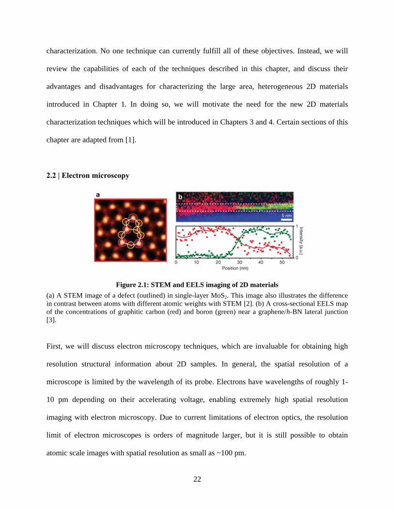
Figure 2.1: STEM and EELS imaging of 2D materials
(a) A STEM image of a defect (outlined) in single-layer MoS2. This image also illustrates the difference
in contrast between atoms with different atomic weights with STEM [2]. (b) A cross-sectional EELS map
of the concentrations of graphitic carbon (red) and boron (green) near a graphene/h-BN lateral junction
[3].
First, we will discuss electron microscopy techniques, which are invaluable for obtaining high
resolution structural information about 2D samples. In general, the spatial resolution of a
microscope is limited by the wavelength of its probe. Electrons have wavelengths of roughly 1-
10 pm depending on their accelerating voltage, enabling extremely high spatial resolution
imaging with electron microscopy. Due to current limitations of electron optics, the resolution
limit of electron microscopes is orders of magnitude larger, but it is still possible to obtain
atomic scale images with spatial resolution as small as ~100 pm.
Page 39
23
In particular, the transmission electron microscope is an extremely powerful tool for
producing structural and compositional mapping of materials on an atomic scale. Several
different modes of operation are available, each with different capabilities. First, scanning
transmission electron microscopy (STEM), where an incident electron beam is focused to a
subnanometer-sized spot and raster scanned across the sample, has been used by a number of
groups to produce atomic resolution images of 2D materials [4,5]. In this mode, the contrast of
each atom increases with increasing atomic number, allowing different elements to be
distinguished in 2D materials such as TMDs [2,6] and h-BN [4]. STEM is particularly useful for
imaging lattice defects, such as grain boundaries [2,5-7]. Figure 2.1a shows a defect in single
layer MoS2 which was imaged with STEM, and also illustrates the contrast difference between
the heavy Mo (bright) and light S (dark) atoms.
Electron energy loss spectroscopy (EELS) is a complementary spectroscopy technique to
STEM. By measuring the energies lost by the monochromated electrons transmitted through the
sample, EELS can determine local information about atomic composition and bonding. For
example, subtle changes in EELS spectra can be used to differentiate between graphitic and
amorphous carbon [3,8]. A higher signal to noise ratio EELS signal can be obtained for thicker
materials, and thus EELS has been used to map the chemical composition in cross sections of
lateral [3] and vertical [8,9] 2D heterostructures. Figure 2.1b shows a cross-sectional EELS map
of a patterned lateral graphene/h-BN junction, plotting the concentrations of graphitic carbon
(red) and boron (green). Here, EELS was used to establish a junction width between the
patterned graphene and h-BN regions of <10 nm.
Conventional transmission electron microscopy (CTEM, or simply TEM) is also very
valuable for 2D materials characterization. In this mode of imaging, a larger area of the sample
Page 40
24
(e.g. several microns) is illuminated with the electron beam. Like STEM, aberration corrected
high resolution TEM (HR-TEM) can also be used to obtain atomic resolution images of 2D
materials [10-12], although it is more difficult to quantitatively interpret the image contrast in
this mode. Another particularly useful feature of TEM for 2D materials characterization is the
ability to obtain an electron diffraction pattern, which can be used to identify the local
crystallinity and orientation of the sample [5,7]. Single crystals of monolayer graphene, h-BN,
and TMDs all produce six-fold symmetric diffraction patterns.
Figure 2.2: Dark-field TEM imaging of graphene
(a) A conventional TEM image of a suspended graphene film, which is largely featureless and transparent
to the electron beam. (b) An electron diffraction pattern from the same region, showing many sets of six-
fold symmetric diffraction spots. The circle indicates the location of the aperture for (c), the dark-field
image of the grains corresponding to the selected crystalline orientation. (d) and (e) illustrate false colored
imaging of graphene grains with many different orientations. Scale bars 500 nm [5].
A related mode of operation, dark-field TEM imaging (DF-TEM), can be used to
visualize the individual crystalline grains of 2D materials (Figure 2.2) [5,13,14]. After obtaining
a diffraction pattern from the sample, an objective aperture is placed in the diffraction plane so
that only electrons scattered in a certain direction are collected. In the final real space image,
only those regions with the selected orientation are visible. This technique can be extended to
identify all of the grains in the sample by taking a series of images where the aperture is moved
to select different diffraction spots. DF-TEM can also be used to identify the relative orientations
of stacked layers; for misoriented layers, the grains corresponding to two different diffraction
Page 41
25
spots will overlap spatially. Typically, these images are compiled into a composite which is false
colored by orientation, as in Figure 2.2e. DF-TEM will be used extensively in this dissertation to
characterize the grain structure and stacking order in a variety of 2D samples.
The biggest disadvantage to all transmission electron microscopy techniques is that they
have restrictive sample preparation requirements, which can limit their use in materials
characterization. First, the entire sample must be transparent to electrons, which limits the
potential substrates to very thin membranes (e.g. 5-10 nm of silicon nitride) or suspended
samples. The samples should also be free of contaminants, particularly hydrocarbon residues, for
atomic resolution STEM and HR-TEM imaging. All electron microscopy techniques are also
potentially destructive: they can deposit amorphous carbon on the sample surface, dope the
sample, and cause damage to the lattice, depending on the material being studied and the
accelerating voltage of the electron beam.
Figure 2.3: SEM of graphene
A SEM image of CVD graphene on its copper growth substrate [15]
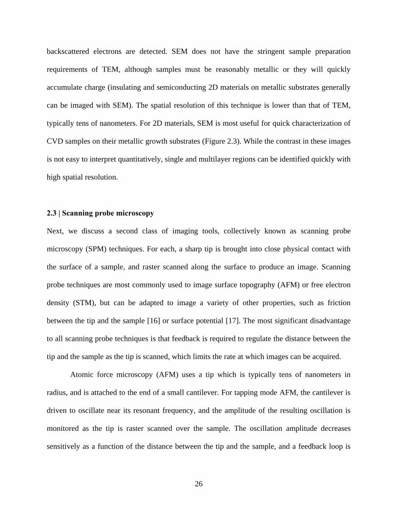
A final electron microscopy technique of note is scanning electron microscopy (SEM),
where the electron beam is focused and raster scanned along the surface of the sample, and
Page 42
26
backscattered electrons are detected. SEM does not have the stringent sample preparation
requirements of TEM, although samples must be reasonably metallic or they will quickly
accumulate charge (insulating and semiconducting 2D materials on metallic substrates generally
can be imaged with SEM). The spatial resolution of this technique is lower than that of TEM,
typically tens of nanometers. For 2D materials, SEM is most useful for quick characterization of
CVD samples on their metallic growth substrates (Figure 2.3). While the contrast in these images
is not easy to interpret quantitatively, single and multilayer regions can be identified quickly with
high spatial resolution.
2.3 | Scanning probe microscopy
Next, we discuss a second class of imaging tools, collectively known as scanning probe
microscopy (SPM) techniques. For each, a sharp tip is brought into close physical contact with
the surface of a sample, and raster scanned along the surface to produce an image. Scanning
probe techniques are most commonly used to image surface topography (AFM) or free electron
density (STM), but can be adapted to image a variety of other properties, such as friction
between the tip and the sample [16] or surface potential [17]. The most significant disadvantage
to all scanning probe techniques is that feedback is required to regulate the distance between the
tip and the sample as the tip is scanned, which limits the rate at which images can be acquired.
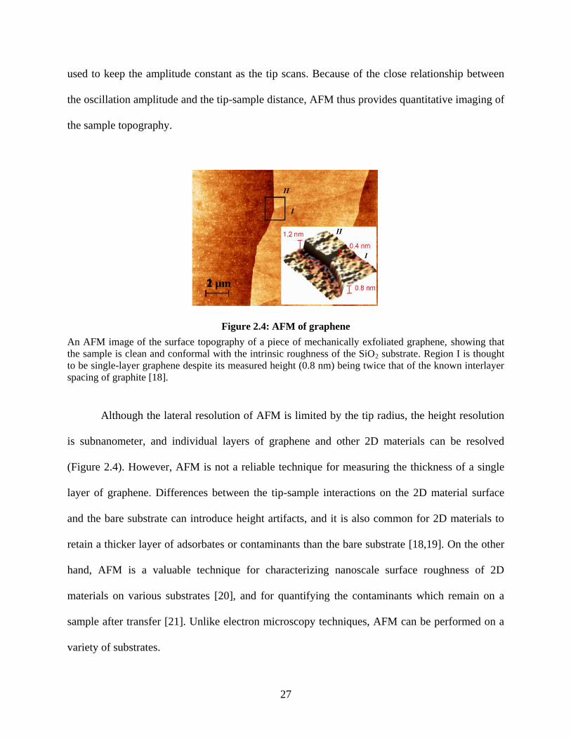
Atomic force microscopy (AFM) uses a tip which is typically tens of nanometers in
radius, and is attached to the end of a small cantilever. For tapping mode AFM, the cantilever is
driven to oscillate near its resonant frequency, and the amplitude of the resulting oscillation is
monitored as the tip is raster scanned over the sample. The oscillation amplitude decreases
sensitively as a function of the distance between the tip and the sample, and a feedback loop is
Page 43
27
used to keep the amplitude constant as the tip scans. Because of the close relationship between
the oscillation amplitude and the tip-sample distance, AFM thus provides quantitative imaging of
the sample topography.
Figure 2.4: AFM of graphene
An AFM image of the surface topography of a piece of mechanically exfoliated graphene, showing that
the sample is clean and conformal with the intrinsic roughness of the SiO2 substrate. Region I is thought
to be single-layer graphene despite its measured height (0.8 nm) being twice that of the known interlayer
spacing of graphite [18].
Although the lateral resolution of AFM is limited by the tip radius, the height resolution
is subnanometer, and individual layers of graphene and other 2D materials can be resolved
(Figure 2.4). However, AFM is not a reliable technique for measuring the thickness of a single
layer of graphene. Differences between the tip-sample interactions on the 2D material surface
and the bare substrate can introduce height artifacts, and it is also common for 2D materials to
retain a thicker layer of adsorbates or contaminants than the bare substrate [18,19]. On the other
hand, AFM is a valuable technique for characterizing nanoscale surface roughness of 2D
materials on various substrates [20], and for quantifying the contaminants which remain on a
sample after transfer [21]. Unlike electron microscopy techniques, AFM can be performed on a
variety of substrates.
2 µm
Page 44
28
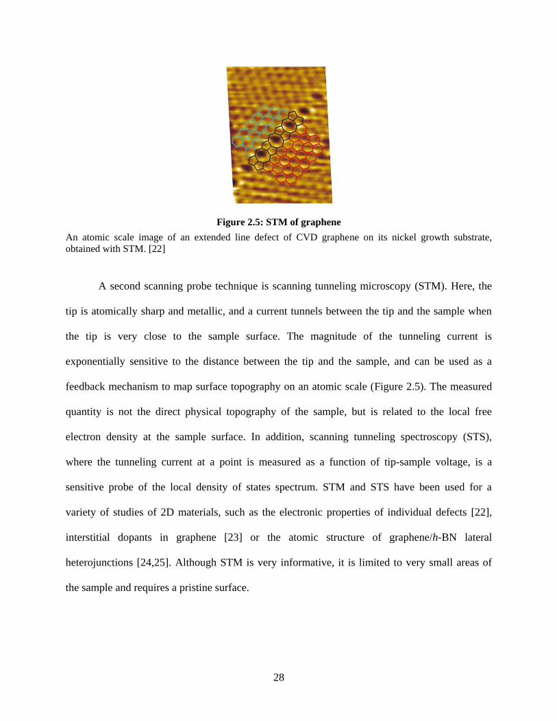
Figure 2.5: STM of graphene
An atomic scale image of an extended line defect of CVD graphene on its nickel growth substrate,
obtained with STM. [22]
A second scanning probe technique is scanning tunneling microscopy (STM). Here, the
tip is atomically sharp and metallic, and a current tunnels between the tip and the sample when
the tip is very close to the sample surface. The magnitude of the tunneling current is
exponentially sensitive to the distance between the tip and the sample, and can be used as a
feedback mechanism to map surface topography on an atomic scale (Figure 2.5). The measured
quantity is not the direct physical topography of the sample, but is related to the local free
electron density at the sample surface. In addition, scanning tunneling spectroscopy (STS),
where the tunneling current at a point is measured as a function of tip-sample voltage, is a
sensitive probe of the local density of states spectrum. STM and STS have been used for a
variety of studies of 2D materials, such as the electronic properties of individual defects [22],
interstitial dopants in graphene [23] or the atomic structure of graphene/h-BN lateral
heterojunctions [24,25]. Although STM is very informative, it is limited to very small areas of
the sample and requires a pristine surface.
Page 45
29
2.4 | Optical microscopy
Optical microscopy techniques, a third class of imaging tools, have several advantages over both
electron microscopy and scanning probe techniques. Not only can images be acquired rapidly,
allowing large-scale imaging with high throughput, but optical microscopy also requires
minimum sample preparation and causes little to no damage to the sample. Light can interact
with a sample through a variety of processes, which can provide spectroscopic information
probing the material’s electronic and vibrational properties.
However, the most significant limitation of optical microscopy is that the spatial
resolution of the collected images is limited by the wavelength of the light, which is much larger
than the wavelength of an electron. In practice, the resolution limit is a few hundred nanometers
for visible light illumination, which is orders of magnitude larger than many features of interest
in 2D materials, such as single atomic defects or individual grain boundaries. On the other hand,
this resolution is still significantly smaller than the typical grain size of high quality CVD-grown
2D materials, and is more than sufficient for many studies.
Figure 2.6: Making graphene visible
(left) Color (a) and single wavelength (b) images of exfoliated graphene on a silicon wafer with a 300 nm
SiO2 layer. In both cases, single- and few-layer graphene are visible and can be differentiated. (right) A
plot illustrating the contrast of graphene (color scale) at different wavelengths (y-axis) and SiO2
thicknesses (x-axis) [26].
Page 46
30
One of the most crucial applications of optical imaging for the field of 2D materials
research was also one of the simplest, and this example highlights the benefits of the high
throughput and simplicity of optical microscopy. Particularly during the early development of
the 2D materials field when graphene samples were produced by mechanical exfoliation, it was
necessary to be able to search a large region of a substrate quickly in order to identify areas of
single- and few-layer graphene among many thicker regions. This is difficult because a single
layer of graphene absorbs only 2.3% of visible light. However, if silicon with an appropriate
oxide thickness is used as a substrate, interference effects can increase the contrast of the single-
layer graphene to roughly 10% under white light illumination, making it visible by eye (Figure
2.6) [26,27]. This technique allowed the rapid identification of single- and few-layer exfoliated
graphene for use in further studies, and is still widely used for imaging both CVD graphene and
many semiconducting 2D materials after transfer. However, we note that this technique is poorly
suited for identifying single- and few-layer h-BN, which is transparent at all visible energies; we
will discuss this point in more detail in Chapter 3.
While white light microscopy is sufficient for certain applications, it is not sensitive
enough to image the complex variations in composition and structure which can be present in 2D
materials. Instead, as we will discuss in the following chapters, understanding how a 2D material
interacts with light as a function of wavelength can provide very detailed information about its
composition, number of layers, stacking structure, and defect density. The spectral response of a
material can be obtained by scanning the optical excitation wavelength (λex) using a tunable
source. At a fixed λex, the spectrum of any emitted light from the sample can also be collected,
providing information about inelastic optical processes such as photoluminescence and Raman
Page 47
31
scattering. Microscopy techniques which provide both spatial and spectral information about a
sample are referred to as imaging spectroscopy or hyperspectral imaging techniques.
Both electron microscopy and scanning probe techniques can also provide information
about the energy-dependent response of a sample. However, EELS suffers from low spectral
resolution (typically >0.1 eV), and STS from a limited energy range (1-2 eV). On the other hand,
wavelengths for optical characterization range from the near infrared (~800-2500 nm, or 0.5-1.5
eV) and visible (~400-800 nm, or 1.5-3 eV) to the ultraviolet (~200-400 nm, or 3-6 eV), and a
spectral resolution of <0.01 eV is easily achievable. Thus, in addition to its high throughput and
versatility, the large spectral range and high spectral resolution of optical microscopy are
additional advantages to this class of characterization techniques.
2.5 | Outlook
To summarize, we have reviewed three classes of imaging techniques: electron, scanning probe,
and optical microscopy. While both electron microscopy and scanning probe techniques have
provided direct images of a variety of atomic and nanometer-scale structural features in 2D
materials, these non-optical techniques also have several disadvantages. Scanning probe
techniques are generally slow, limiting their ability to characterize graphene over a large area,
while electron microscopy techniques have the potential to alter or damage the sample. AFM and
SEM provide limited information about atomic structure, while more informative techniques
such as STM and TEM require restrictive sample preparation, precluding many device
geometries. None of these techniques alone is sufficient to quickly and non-destructively image a
large area 2D sample.
Page 48
32
Optical microscopy has the potential to bridge this gap, and the high throughput,
simplicity, and versatility of white light optical microscopy have already made it the tool of
choice for simply visualizing CVD or exfoliated graphene on a silicon substrate. However,
imaging spectroscopy is required in order to take full advantage of the sensitivity of optical
microscopy. For this, hyperspectral microscopes can be designed to exploit the known optical
responses of various 2D materials. Examples which we will discuss in the following chapters
include the variations in the optical absorption spectra of 2D materials with different atomic
compositions, such as graphene and h-BN, and the inelastic Raman scattering spectrum of
graphene, which is sensitive to parameters such as point defect density, doping, strain, and
stacking structure.
Next, these same microscopes can be used to quantitatively characterize the optical
response of an arbitrary 2D material with unknown compositional or structural features.
Combined with the direct, nanometer scale imaging capabilities of electron microscopy and
scanning probe techniques, we can establish new relationships between the structure and
properties of a variety of complex 2D materials, enabling the discovery of new physics and
functionalities in these systems. In the following chapters, we will use DF-TEM imaging
extensively to compare the grain structure and stacking orientations of our samples to their
optical absorption and Raman scattering spectra. We will also use AFM to examine the effects of
contaminants on the optical properties of our samples, and compare some of our optical data with
previous STM and STS studies of similar systems.
Optical imaging spectroscopy is not a new concept, and a variety of imaging
spectroscopy techniques have already been applied to 2D materials research. However, there are
a number of specific technical challenges which have prevented these techniques from being
Page 49
33
used to their full potential for characterizing complex 2D materials on a large scale. In Chapters
3 and 4, we discuss and address these challenges in order to adapt absorption spectroscopy and
Raman spectroscopy, respectively, as diffraction-limited microscopy techniques optimized for
2D materials characterization.
Page 50
34
References
[1] R. Havener, A. Tsen, H. Choi, and J. Park, NPG Asia Materials 3, 91 (2011).
[2] S. Najmaei et al., Nature Materials 12, 754 (2013).
[3] M. Levendorf, C. Kim, L. Brown, P. Huang, R. Havener, D. Muller, and J. Park, Nature
488, 627 (2012).
[4] O. Krivanek et al., Nature 464, 571 (2010).
[5] P. Huang et al., Nature 469, 389 (2011).
[6] A. van der Zande et al., Nature Materials 12, 554 (2013).
[7] K. Kim, Z. Lee, W. Regan, C. Kisielowski, M. Crommie, and A. Zettl, ACS Nano 5, 2142
(2011).
[8] L. Wang et al., Science 342, 614 (2013).
[9] S. J. Haigh et al., Nature Materials 11, 764 (2012).
[10] J. Meyer, C. Kisielowski, R. Erni, M. Rossell, M. Crommie, and A. Zettl, Nano Letters 8,
3582 (2008).
[11] A. Gibb, N. Alem, J. Chen, K. Erickson, J. Ciston, A. Gautam, M. Linck, and A. Zettl,
Journal of the American Chemical Society 135, 6758 (2013).
[12] A. Hashimoto, K. Suenaga, A. Gloter, K. Urita, and S. Iijima, Nature 430, 870 (2004).
[13] L. Brown, R. Hovden, P. Huang, M. Wojick, D. A. Muller, and J. Park, Nano Letters 12,
1609 (2012).
[14] A. Tsen et al., Science 336, 1143 (2012).
[15] X. Li, C. Magnuson, A. Venugopal, R. Tromp, J. Hannon, E. Vogel, L. Colombo, and R.
Ruoff, Journal of the American Chemical Society 133, 2816 (2011).
[16] A. J. Marsden, M. Phillips, and N. R. Wilson, Nanotechnology 24, 255704 (2013).
[17] S. S. Datta, D. R. Strachan, E. J. Mele, and A. T. C. Johnson, Nano Letters 9, 7 (2009).
[18] Y. Zhang, Y. Tan, H. Stormer, and P. Kim, Nature 438, 201 (2005).
[19] K. Novoselov, A. Geim, S. Morozov, D. Jiang, Y. Zhang, S. Dubonos, I. Grigorieva, and
A. Firsov, Science 306, 666 (2004).
[20] C. Lui, L. Liu, K. Mak, G. Flynn, and T. Heinz, Nature 462, 339 (2009).
[21] J. Song, F. Kam, R. Png, W. Seah, J. Zhuo, G. Lim, P. Ho, and L. Chua, Nature
Nanotechnology 8, 356 (2013).
Page 51
35
[22] J. Lahiri, Y. Lin, P. Bozkurt, I. Oleynik, and M. Batzill, Nature Nanotechnology 5, 326
(2010).
[23] L. Zhao et al., Science 333, 999 (2011).
[24] P. Sutter, R. Cortes, J. Lahiri, and E. Sutter, Nano Letters 12, 4869 (2012).
[25] L. Liu et al., Science 343, 163 (2014).
[26] P. Blake, E. Hill, A. Neto, K. Novoselov, D. Jiang, R. Yang, T. Booth, and A. Geim,
Applied Physics Letters 91, 063124 (2007).
[27] K. Novoselov, D. Jiang, F. Schedin, T. Booth, V. Khotkevich, S. Morozov, and A. Geim,
PNAS 102, 10451 (2005).
Page 52
36
Chapter 3 : DUV-VIS-NIR HYPERSPECTRAL IMAGING
3.1 | Introduction
In this chapter, we describe a hyperspectral optical microscope whose excitation wavelength
(λex) can be tuned continuously over an energy range of several electron volts (eV). By obtaining
the spatially resolved transmission or reflection spectrum of a 2D sample, we can characterize
and distinguish between regions with different optical absorption spectra. Here, we will focus on
the use of our microscope to image 2D heterostructures with spatially varying composition,
specifically patterned graphene/h-BN lateral junctions. However, the imaging and quantitative
spectroscopy techniques we describe in this chapter can immediately be applied to many other
2D systems, and we will explore the use of this microscope to characterize the optical properties
of twisted bilayer graphene (tBLG) over a large energy range in Chapters 5 and 6.
The challenge of building this microscope was to provide a large enough energy range to
observe the relevant spectral features for a diverse group of 2D materials and 2D
heterostructures. Standard optical microscopes are designed to operate using visible or infrared
light at energies below ~3 eV. However, many 2D materials contain important features in their
optical absorption spectra at much higher energies, as we discuss in more detail below. In
particular, h-BN is an insulator which is completely transparent at energies below 6.1 eV, or at
wavelengths longer than 203 nm. Operating at these deep ultraviolet (DUV) energies required
the careful selection of the illumination source, optical elements, and array detector for our setup.
Our DUV-Vis-NIR hyperspectral microscope provides imaging and spectroscopy at
energies of up to 6.2 eV, allowing direct optical imaging of h-BN at its absorption peak for the
first time, and comprehensive, all-optical mapping of chemical composition in graphene/h-BN
Page 53
37
lateral heterojunctions. With the addition of dark-field transmission electron microscopy (DF-
TEM), we obtain quantitative structure-property relationships, confirming the formation of
interfaces in graphene/h-BN lateral heterojunctions which are abrupt on a submicron scale. In
particular, we outline a procedure for obtaining the quantitative full optical function (σ) of 2D
materials which sit on thin silicon nitride membranes, a substrate which is also compatible with
TEM imaging. We also perform hyperspectral imaging of samples that are supported on a
nontransparent silicon/SiO2 substrate, enabling facile fabrication of atomically thin electronic
devices with known composition and structure. The majority of this chapter is reproduced from
[1], as well as certain sections from [2].
3.2 | Absorption spectroscopy
Optical absorption spectroscopy can provide information about the band structure of a material
over an energy range of several eV, and serves as a useful fingerprint to identify the composition
of a material. When any material absorbs a photon, a transition can only occur between two
states in the electronic band structure of the material with the same momentum. Thus, optical
absorption is closely related to the density of states of a material. Because of this, materials with
varying band gaps, such as metals, semiconductors, and insulators, typically have very distinct
optical absorption spectra [3].
The optical response of any material is actually described by its optical conductivity (σ)
through the equation J = σE, where J is the current density in the material and E is the time-
dependent electric field of the incoming light. In general, σ is an imaginary quantity whose real
part is proportional to the optical absorption of the material, and whose imaginary part is
proportional to its permittivity. Although Re[σ] is often the quantity of interest, Re[σ] and Im[σ]
Page 54
38
are linked through mathematical rules known as the Kramers-Kronig relations [4], such that a
material with features (such as peaks) in its absorption spectrum will also exhibit corresponding
features in its Im[σ] spectrum.
This distinction is important because absorption (i.e. Re[σ]) is never measured directly.
Rather, the measured quantity is the transmission through or reflection from the sample as a
function of wavelength. The case of 2D materials is further complicated by the fact that 2D
samples are typically supported by a bulk substrate. Depending on the substrate used, the
measured reflection or transmission spectrum of the entire sample may be a function of both
Re[σ] and Im[σ] of the 2D material. For some substrates, such as transparent fused silica, it is
straightforward to convert the transmission or reflection spectrum of the 2D material and its
supporting substrate to Re[σ] of the 2D material alone [5], while for others, such as a silicon
wafer with an oxidized surface layer, it is much more difficult. These challenges will be
discussed in more detail in Section 3.5.
Figure 3.1: Optical absorption in graphene
(left) A schematic of an allowed optical transition in graphene. (center) An image of transmitted light
through a suspended single and bilayer graphene sample, and (right) a plot of the transmittance vs.
wavelength, illustrating that this quantity is constant over the visible range. [6]
Page 55
39
The optical absorption spectrum of graphene is unique due to the cone-like linear
dispersion of its conduction and valence bands near its charge neutrality (Dirac) point (Figure
3.1). Single layer graphene has a uniform optical absorption at most visible and near infrared
wavelengths [6] of 2.3% or πα, where α is the fine structure constant, while thin multilayers
exhibit multiples of 2.3% absorption (Figure 3.1 right, inset). While 2.3% absorption is nearly
transparent to the eye, it is fairly large considering that the material is only one atom thick. The
finite visible light absorption of graphene enabled the use of a simple optical microscopy
technique to visualize it, as described in Chapter 2.
Figure 3.2: UV absorption spectra of graphene and h-BN
The UV absorption spectrum of monolayer graphene and h-BN transferred to a quartz substrate, measured
across a large area (several mm) with a UV-Vis-NIR spectrometer. We note that the low energy optical
response of graphene (red) is not accurate in this particular measurement, as monolayer graphene has a
constant 0.023 absorbance at visible energies (see above). [7]
On the other hand, semiconducting and insulating materials are generally transparent at
energies below their band gap, and exhibit an absorption peak at their optical band gap energy, as
well as other higher energies where the band structure contains van Hove singularities (vHSs). In
particular, h-BN is transparent at energies of up to 6.1 eV [1,7] due to its large band gap, as
shown by the optical absorption spectrum in Figure 3.2. This makes monolayer h-BN very
Page 56
40
difficult to visualize with visible light [8]. A high energy, saddle point vHS is also present in the
band structure of graphene, leading to a broad, asymmetric peak in its absorption spectrum near
4.6 eV [9,10].
Absorption spectroscopy has been an essential tool for studying the band structures and
many-body interactions in several 2D materials, and has revealed a variety of rich physics in
these low-dimensional systems. However, most absorption studies of 2D materials, particularly
those encompassing UV wavelengths, have been bulk [7] or point [9,10] measurements. Here,
we build an optical microscope capable of DUV-Vis-NIR imaging with submicron spatial
resolution, allowing us to take advantage of the sensitivity of absorption spectroscopy in order to
study 2D materials with complex structural and compositional variations.
3.3 | Details of the DUV-Vis-NIR microscope
Our DUV-Vis-NIR microscope enables hyperspectral imaging of 2D heterostructures over the
entire spectral range of 1.2 to 6.2 eV while maintaining submicron spatial resolution. While
similar DUV-Vis-NIR hyperspectral imaging systems are commercially available [11], our main
goal with our homebuilt system was a wavelength range which encompassed the 6.1 eV band
gap of h-BN, allowing us to identify and image this material at a wavelength where it was highly
absorptive. We have achieved this goal by careful selection of the microscope components,
described below.
In general, optical imaging techniques are performed using a microscope that is equipped
with an excitation light source and delivery optics (illumination), and an optical detector and
collection optics (detection). The illumination and detection geometries and the specific
components chosen for each optical element depend on the intended application of the
Page 57
41
microscope. Our priority was to choose components which were compatible with DUV light, and
which reduced or eliminated chromatic aberrations. To this end, we removed all refractive
elements and DUV-opaque glass (such as BK7) from the light path, and used exclusively mirror-
based (“catoptric”) [12] optics for light focusing and image formation.
Figure 3.3: Schematic and photographs of DUV-Vis-NIR microscope
(a) A schematic of the microscope. (b) The 1000W Xe lamp housing (black, right) and monochromator
(white, left). (c) A close up image of the parabolic mirrors used to align and focus the light from the
monochromator into the solarization-resistant fiber. (d) An early version of the hyperspectral microscope.
Two illumination schemes are possible, transmission (blue) or reflection (red), depending on where the
fiber is attached to the microscope. The image is detected by the CCD camera (top), which has a detection
range of 200-1000 nm.
For illumination, we chose a UV enhanced 1000 W Xe arc source with a monochromator
(typically set to 2 nm spectral resolution) to select a specific wavelength (Figure 3.3). Light
exiting the monochromator is focused with parabolic mirrors (Figure 3.3b) into a multimode
fiber designed not to degrade in performance under exposure to DUV light (solarization-
resistant), which delivers the light to the microscope.
The final key component of the illumination path is a reflective (Schwarzchild) objective
(Figure 3.4). There are two issues for using typical refractive microscope objectives for UV
Page 58
42
imaging. First, as noted above, many glasses strongly absorb UV light. Second, even DUV-
compatible glasses such as pure fused quartz have high dispersion at UV wavelengths, meaning
that their refractive indices change rapidly as a function of wavelength. As a result, the focus of
the microscope would have to be adjusted continuously as λex was varied. Our choice of a
reflective objective avoids both of these problems. Collimated light from the fiber is focused by
the objective onto the sample. The size of the illuminated region is determined by the finite size
of the incoherent light source, which is the core diameter of the delivery fiber in this case. In our
microscope, this results in a ~70 µm diameter circle of illumination on our sample surface
(Figure 3.5). The spatially uneven illumination of our sample is one of the disadvantages of our
design, but all of our images are normalized with respect to a bare substrate to correct for
variations in illumination intensity.
Our microscope is designed to work in one of two modes: reflection or transmission. In
reflection mode (see red line in Figure 3.3, as well as Figure 3.9), a DUV 50/50 beamsplitter
directs the light to illuminate the sample through the objective, after which the reflected light
from the sample is collected through the same objective and directed back through the
microscope. In transmission mode, a second reflective objective below the sample delivers the
light, acting as a condenser. In both cases, the light from the sample is focused onto a one
megapixel charge-coupled device (CCD) for detection, with an effective magnification of ~100×.
Our CCD detector is UV enhanced, allowing detection from 200-1000 nm. For wavelengths
below 250 nm, an additional DUV bandpass filter is required to remove stray visible light, which
originates from the monochromator and/or fiber. For wavelengths from 500-1000 nm, a single
long pass filter may be used to remove the light from second order diffraction (λ = λex/2) in the
monochromator.
Page 59
43
Figure 3.4: Reflective objective
A cross-sectional schematic of the reflective objective used our microscope, taken from the manufacturer
[13]. The white regions are mirrors, while the blue dashed line is the path of the light. Collimated light
enters the objective through the right side and is focused by the curved mirrors onto a point on the left.
The central mirror (left) acts to obscure light traveling directly down the center of the objective, and the
focused light leaving the objective has the form of a hollow cone.
Figure 3.5: Sample illumination and image normalization
An image of multilayer graphene in transmission mode before and after normalization.
Finally, the spatial resolution of an optical microscope is typically determined by the
numerical aperture (N.A.) of the objective, which is the sine of the angle (θ) of the cone of light
which can be collected from a point on the sample. However, the central mirror of a
Schwarzschild objective obscures the central portion of the collected light cone (Figure 3.4). The
result for imaging is that the performance of the objective is somewhat degraded, compared to
that of a refractive objective with the same N.A., when imaging larger features (>λ/N.A. for our
Page 60
44
objective, which has an obscuration of 16.7%). However, the performance of both reflective and
refractive objectives with the same N.A. is approximately the same close to the Abbe diffraction
limit (feature size of λ/2N.A.) [14]. The Abbe limit for a refractive objective with N.A. = 0.65 is
0.77λ, and so we approximate the resolution of our reflective objective as λ (30% larger).
3.4 | Monochromatic and hyperspectral imaging
Figure 3.6: Imaging and spectroscopy of graphene/h-BN heterostructures
(a) Optical transmission images of a graphene/h-BN lateral heterostructure at two different energies,
showing energy-dependent features. (b) False color image combining the images from (a), showing a
clear stripe pattern which matches the (inset) intended design. (c) DF-TEM image of the same sample
(from boxed region in (b)), showing the grain structure of the materials present, which reveals a clear
junction. (inset) A representative background subtracted diffraction pattern from a junction region of the
same sample, showing diffraction spots consistent with both graphene and h-BN. (d) Transmission
spectra from three numbered regions outlined in (c) (with respect to the bare substrate, “B”),
corresponding to partial and full h-BN growth and graphene. (e) Transmission spectra taken along the
dashed line in (b), showing clear h-BN and graphene strips with little compositional mixing. All scale
bars are 5 µm.
We next detail the use of our microscope to study graphene/h-BN lateral heterostructures. The
samples studied in our work were produced by the patterned regrowth method [15] and are
supported either by 10 nm thick silicon nitride (SiN) membranes [16] for both optical and TEM
Page 61
45
imaging, or by silicon substrates with thermal oxide. Figure 3.6 shows optical transmission
images of a graphene/h-BN lateral heterojunction transferred to a SiN membrane substrate with
distinct, energy dependent features. Different regions appear darker (with reduced transmission)
at 4.6 and 6.1 eV, which correspond to the known absorption peaks of graphene [9,10] and h-BN
[7], respectively. Because our microscope has no chromatic aberrations, such images can be
easily combined to generate a false color composite, shown in Figure 3.6b. This large-scale
image reveals lateral junctions whose pattern matches the intended design (Figure 3.6b, inset),
and suggests areas of both full and partial h-BN growth immediately adjacent to graphene strips.
The junction formation is confirmed by a DF-TEM [17] image (Figure 3.6c) of same device from
Figure 3.6b (boxed region), in which different colors indicate domains of different crystalline
orientations. This image shows clear lines across which the domain structure changes abruptly,
and confirms that both graphene and h-BN are polycrystalline single layers. We note, however,
that our DF-TEM data alone cannot definitively distinguish between graphene and h-BN,
because the diffraction patterns from both materials have the same symmetry and very similar
lattice constants, as shown in a diffraction pattern from a junction region containing both
materials (Figure 3.6c, inset).
The spatially-resolved atomic composition is confirmed by full spectral measurements
(Figure 3.6d and Figure 3.6e). Figure 3.6d shows transmission spectra taken from several 1 μm
diameter spots (outlined in Figure 3.6c), extracted from hundreds of transmission images of the
same region measured while continuously varying the photon energy from 1.8 to 6.2 eV. The
majority of these hyperspectral images can be acquired within minutes, with an acquisition time
per frame of <1 second for wavelengths above 250 nm, increasing to 1-2 minutes near 200 nm.
Here, we plot 1-T, the transmission contrast (T defined as I/I0, where I0 is the transmission
Page 62
46
intensity through the bare substrate, and I is the intensity through the substrate plus sample),
which is approximately equal to the absorption of the sample in most cases. Regions 1 and 3
exhibit a sharp, narrow peak near 6.1 eV, consistent with h-BN [7], while region 2 exhibits a
broad, asymmetric peak near 4.5 eV with roughly constant 1-T at lower energies, consistent with
graphene [6,9,10]. These results provide the most direct confirmation of our assignments of the
composition in each area and suggest high qualities of graphene and h-BN. Furthermore, a two-
dimensional plot of 1-T vs. energy across the graphene/h-BN heterojunction (Figure 3.6e)
suggests that the transition between the graphene and h-BN is abrupt on a micron scale, and that
each region exhibits a homogeneous optical spectrum, suggesting little compositional mixing.
Thus, our graphene/h-BN heterostructure behaves as designed; additionally, we note that the
optical response of the single-layer h-BN is similar for both partial and full growth regions with
different grain structures, suggesting it is independent of grain size from hundreds of nm to ~1
μm.
3.5 | Quantitative absorption spectroscopy
Our microscope also provides quantitatively accurate, spatially resolved measurements of the
complex optical conductivity (σ) of 2D materials (or permittivity, ε = iσ/ω). Figure 3.7 shows the
real and imaginary parts of σ from our single-layer graphene and h-BN. These values were
extracted from transmission and reflection images of the same sample, and the known optical
parameters and geometry of the SiN substrate, which are discussed in more detail below.
In particular, we found that while 1-T of an atomically thin film on a thin (<<λ)
membrane is approximately proportional to the film’s absorption (or Re[σ]), the reflection
contrast 1-R (where R is defined analogously to T) is instead approximately proportional to
Page 63
47
Im[σ]. Figure 3.8 shows the calculated contrast of an atomically thin (0.34 nm) film in
transmission and reflection modes on a 10 nm thick SiN membrane at 2.5 eV as a function of
Re[σ] and Im[σ] of the atomically thin film. This calculation demonstrates that there is an
approximately linear relationship between contrast and Re[σ] in transmission mode, and between
contrast and Im[σ] in reflection mode. Additionally, there is much less variation in contrast when
the opposite parameter (Im[σ] in transmission mode or Re[σ] in reflection mode) is varied.
Figure 3.7: Quantitative calculation of intrinsic optical conductivity
(a) Measured real and imaginary parts of the optical conductivity (σ) of single-layer CVD graphene and
h-BN. (inset) Measured complex refractive index (n+ik) of CVD graphene (dots), compared with
previous work (lines) [18]. (b) Schematic illustrating phase contrast mechanism for reflection imaging of
atomically thin films on a thin silicon nitride membrane (membrane thickness enlarged for clarity). (c)
Reflection image of graphene/h-BN junction (same region as Figure 3.6c), showing that h-BN is visible
far from its absorption peak in this mode (scale bar 5μm).
A more intuitive explanation for this unusual effect is that the reflections from the front
and back of the thin membrane have opposite phase, interfering destructively [19]; the atomically
thin film acts to alter this phase difference, typically increasing reflection, to a degree which
depends on its thickness and dielectric constant (or Im[σ]) (Figure 3.7b). Due to this effect, h-BN
is clearly visible in reflection mode even at low energies (Figure 3.7c).
Page 64
48
Figure 3.8: Contrast as a function of Re[σ] and Im[σ]
Calculated contrast for an atomically thin film in (left) transmission and (right) reflection mode on a 10
nm thick silicon nitride membrane. For transmission (reflection) mode, the contrast is plotted as a
function of Re[σ] (Im[σ]) while Im[σ] (Re[σ]) is held constant. In the insets, Im[σ] (Re[σ]) varies while
Re[σ] (Im[σ]) is constant.
To calculate the complex σ of our atomically thin samples, we model our substrate +
sample as a series of thin films using the transfer matrix formalism [20], and solve
simultaneously for the values of Re[σ] and Im[σ] which best fit our transmission and reflection
data. We set the incident angle of the unpolarized light in our model to 30° from the normal
(which is the average incident angle produced by our reflective objective), and we assume that a
single layer of graphene or h-BN has a thickness of 0.34 nm, close to the interplanar spacing of
both materials [21,22]. We also find it necessary to add an additional layer to our thin film model
to account for material trapped under the 2D film and/or adsorbates [23], with a thickness of 1-2
nm, to obtain consistent and reasonable results (examples of which are discussed below) when
calculating σ of the atomically thin film. Adding this extra layer effectively increases our
calculated value of Im[σ] by a constant, with little effect on Re[σ].
For simplicity, we assume that the debris is only trapped under the film, not adsorbed on
top of it, and that σ(λ) of the debris is that of PMMA [24]. We choose the thickness of the debris
layer such that our calculated Im[σ] of the atomically thin film meets several criteria: 1. Im[σ] of
Page 65
49
Bernal-stacked bilayer graphene is approximately twice that of single-layer graphene, when
applicable; 2. The real part of the permittivity (ε = iσ/ω) is roughly constant as a function of
energy away from a resonance; 3. The real part of the refractive index n = Re[ε1/2
] at low
energies is consistent with literature values for single-layer graphene [21] and bulk h-BN [25].
Without the extra layer in our model, these criteria are not met. The debris thicknesses that best
meet these criteria for the graphene/h-BN samples discussed in this chapter are 1 nm for the h-
BN and 2 nm for the graphene.
This debris layer introduces uncertainty into our calculation of Im[σ] for our atomically
thin film. Particularly, the dispersion of the debris is unknown, and this will likely introduce the
greatest uncertainty in Im[σ] at high energies where the dispersion of different insulating
materials can vary greatly. Full Kramers-Kronig analysis [4] may be useful in the future to find a
consistent σ(λ) for all materials present.
Despite this uncertainty, the full optical function we calculate for CVD graphene matches
previous, Kramers-Kronig consistent measurements of its refractive index [18] (n+ik = ε1/2
)
(Figure 3.7a, inset). Our data in Figure 3.7a also provide complete quantitative measurements of
σ for single-layer h-BN for the first time, and allow evaluation alongside that of CVD graphene.
Re[σ] of single-layer h-BN peaks at ~9 e2/4ħ (corresponding to ~20% absorption) for 6.11±0.03
eV, and |Im[σ]| peaks at a slightly lower energy with a similar height. Significantly, the accurate
knowledge of σ for arbitrary atomically thin films enhances the capabilities of our microscope,
because it allows us to predict the appearance of the same films on more complicated or non-
transparent substrates for all-optical identification, as detailed in the following section.
Page 66
50
3.6 | Imaging on silicon substrates
Figure 3.9: Reflection spectroscopy on Si/SiO2
(a) Contrast (1-R) of graphene and h-BN on Si/SiO2 (285 nm) for energies of up to 6.1 eV, calculated
using σ from Figure 3.7. (inset) Schematic for imaging samples on Si/SiO2 substrates in reflection mode.
(b) (left) Image of a graphene/h-BN junction on Si/SiO2 (285 nm), illustrating that h-BN is clearly visible
at 6.1 eV, and (right) a false color image combining data at 6.1 and 5.0 eV, showing the relative positions
of graphene and h-BN in this device (scale bar 5 μm).
Our DUV-Vis-NIR hyperspectral microscope can also image and characterize atomically thin
heterostructures on non-transparent substrates for device fabrication, most notably silicon with
an oxide layer, when operating in reflection mode (Figure 3.9a, inset). For monochromatic
imaging, the oxide thickness determines the contrast once σ(λ) of the atomically thin film is
known [21]. Based on our measured σ (Figure 3.7), we calculate (1-R) vs. energy for graphene
and h-BN on 285 nm thick oxide, a substrate which is already widely used for graphene imaging,
in Figure 3.9. Our calculation predicts high contrast for graphene near 2.2, 3.6, and 4.8 eV, while
h-BN exhibits high contrast only near 6.1 eV. This allows rapid imaging of both graphene and h-
BN directly on 285 nm Si/SiO2, as demonstrated in Figure 3.9b. We note that h-BN should be
visible at 6.1 eV for most oxide thicknesses, including on bare silicon, except for a few specific
cases (near (54 + 66α) nm, where α is an integer).
Page 67
51
3.7 | Conclusion
In conclusion, our DUV-Vis-NIR hyperspectral microscope provides a versatile platform for
imaging and characterization of arbitrary 2D heterostructures. While we focused on graphene/h-
BN junctions in this chapter, the optical and TEM characterization methods demonstrated here
can be immediately applied for the study of heterostructures formed between other 2D materials.
In particular, we will discuss the possible applications of this microscope to study MoS2 and
other TMD heterostructures in more detail in Chapter 7. Recent theoretical work has predicted
exciting optical and electronic properties in many such systems which have yet to be
characterized [26-28], and our technique provides an essential tool for developing complex 2D
devices with highly controlled, tunable functionalities.
Additionally, in multilayer stacks of 2D materials, interlayer interactions can generate
additional structure-dependent optical features [29-35]. An important example is twisted bilayer
graphene, which exhibits multiple additional absorption peaks at DUV and visible energies,
depending on its twist angle (θ) [32-35]. Our microscope has been essential for quantitative
characterization of the optical properties of tBLG as a function of θ, establishing precise
structure-property relationships in this material. More details of this application of our
microscope will be described in Chapters 5 and 6.
Page 68
52
References
[1] R. W. Havener, C. J. Kim, L. Brown, J. W. Kevek, J. D. Sleppy, P. L. McEuen, and J.
Park, Nano Letters 13, 3942 (2013).
[2] R. Havener, A. Tsen, H. Choi, and J. Park, NPG Asia Materials 3, 91 (2011).
[3] P. Y. Yu and M. Cardona, Fundamentals of semiconductors: physics and materials
properties (Springer, 1996).
[4] J. D. Jackson, Classical Electrodynamics (John Wiley & Sons, Hoboken, NJ, 1999).
[5] K. F. Mak, M. Y. Sfeir, Y. Wu, C. H. Lui, J. A. Misewich, and T. F. Heinz, Physical
Review Letters 101, 196405 (2008).
[6] R. Nair, P. Blake, A. Grigorenko, K. Novoselov, T. Booth, T. Stauber, N. Peres, and A.
Geim, Science 320, 1308 (2008).
[7] K. Kim et al., Nano Letters 12, 161 (2012).
[8] R. Gorbachev et al., Small 7, 465 (2011).
[9] K. Mak, J. Shan, and T. Heinz, Physical Review Letters 106, 046401 (2011).
[10] D. Chae, T. Utikal, S. Weisenburger, H. Giessen, K. von Klitzing, M. Lippitz, and J.
Smet, Nano Letters 11, 1379 (2011).
[11] Craic Technologies Microspectrophotometer & Microspectrometer. Web. 21 Jun 2014.
<http://www.microspectra.com/>
[12] R. Barker, Philosophical Transactions 39, 259 (1735).
[13] Schematic of reflective objective. Illustration. n.d. Adjustable ReflX Objective
52X/0.65NA DUV, Finite. Edmund Optics. Web. 21 Jun 2014.
[14] G. Nadorff and F. DeWitt. Reflaxicon objectives for imaging,
<https://cvimellesgriot.com/products/Documents/TechnicalGuide/CVIMGReflaxicon_Whitepap
er.pdf> (2012).
[15] M. Levendorf, C. Kim, L. Brown, P. Huang, R. Havener, D. Muller, and J. Park, Nature
488, 627 (2012).
[16] L. Brown, R. Hovden, P. Huang, M. Wojick, D. A. Muller, and J. Park, Nano Letters 12,
1609 (2012).
[17] P. Huang et al., Nature 469, 389 (2011).
[18] F. Nelson, V. Kamineni, T. Zhang, E. Comfort, J. Lee, and A. Diebold, Applied Physics
Letters 97, 253110 (2010).
Page 69
53
[19] J. Overbeek, Journal of Physical Chemistry 64, 1178 (1960).
[20] S. Roddaro, P. Pingue, V. Piazza, V. Pellegrini, and F. Beltram, Nano Letters 7, 2707
(2007).
[21] P. Blake, E. Hill, A. Neto, K. Novoselov, D. Jiang, R. Yang, T. Booth, and A. Geim,
Applied Physics Letters 91, 063124 (2007).
[22] Y. Shi et al., Nano Letters 10, 4134 (2010).
[23] M. Bruna and S. Borini, Journal of Physics D-Applied Physics 42, 175307 (2009).
[24] M. Ispirian, S. Karabekyan, and R. Eckmann. Cyro Industries Inc. data tabulated by
luxpop.com, <http://www-hera-b.desy.de/subgroup/detector/rich/rich/lens_system Filename:
plastic_trans.ps> (2012).
[25] E. Franke, M. Schubert, J. Hecht, H. Neumann, T. Tiwald, D. Thompson, H. Yao, J.
Woollam, and J. Hahn, Journal of Applied Physics 84, 526 (1998).
[26] J. Yan, K. W. Jacobsen, and K. S. Thygesen, Physical Review B 86, 039910 (2012).
[27] K. Kośmider and J. Fernández-Rossier, Physical Review B 87, 075451 (2012).
[28] H. Park, A. Wadehra, J. Wilkins, and A. Neto, Applied Physics Letters 100, 253115
(2012).
[29] K. Mak, C. Lee, J. Hone, J. Shan, and T. Heinz, Physical Review Letters 105, 136805
(2010).
[30] K. F. Mak, C. H. Lui, J. Shan, and T. F. Heinz, Physical Review Letters 102, 4 (2009).
[31] Y. Zhang, T. Tang, C. Girit, Z. Hao, M. Martin, A. Zettl, M. Crommie, Y. Shen, and F.
Wang, Nature 459, 820 (2009).
[32] J. T. Robinson, S. W. Schmucker, C. B. Diaconescu, J. P. Long, J. C. Culbertson, T.
Ohta, A. L. Friedman, and T. E. Beechem, ACS Nano 7, 637 (2012).
[33] R. Havener, H. Zhuang, L. Brown, R. Hennig, and J. Park, Nano Letters 12, 3162 (2012).
[34] Y. Wang, Z. Ni, L. Liu, Y. Liu, C. Cong, T. Yu, X. Wang, D. Shen, and Z. Shen, ACS
Nano 4, 4074 (2010).
[35] P. Moon and M. Koshino, Physical Review B 87, 205404 (2013).
Page 70
54
Chapter 4 : WIDEFIELD RAMAN IMAGING
4.1 | Introduction
Raman spectroscopy has been used extensively to study graphene and other sp2-bonded carbon
materials, and can provide quantitative information about a variety of parameters including
defect density, strain, doping, layer number, and stacking order in graphene samples. However,
the imaging capabilities of standard Raman spectroscopy techniques are limited by their low
throughput. In this chapter, we apply an existing alternative imaging mode, widefield Raman
imaging, to rapidly visualize and characterize graphene films on arbitrary substrates. We show
that this technique can be used to image graphene orders of magnitude faster than conventional
micro-Raman imaging allows, while still obtaining detailed spectral information about the
sample.
Then, we showcase the advantages of widefield Raman imaging in several important
applications, which establish this tool as a powerful and versatile characterization method for
graphene at different stages of growth and device fabrication. First, we show that unlike white
light optical microscopy, widefield Raman imaging can be used to rapidly and clearly visualize
graphene on a variety of substrates, including unoxidized silicon and copper, as well as
suspended graphene. Second, we demonstrate that widefield Raman is a valuable tool to
characterize the quality of CVD graphene, revealing spatial inhomogeneities in film quality that
could easily go undetected with point Raman spectroscopy. Finally, we use our microscope to
monitor dynamic processes in graphene with high spatial and spectral resolution over a large area
in real time. These novel implementations of widefield Raman for graphene imaging provide
valuable information that cannot be easily obtained with other optical imaging methods, and
Page 71
55
enable new experiments at various stages of graphene growth and processing. The majority of
this chapter is reproduced from [1].
4.2 | Raman spectroscopy
Raman scattering (technically, Stokes Raman scattering) is an inelastic process which occurs
when an absorbed photon loses a small portion of its energy to a vibrational mode (phonon) in a
material, and a corresponding redshifted photon is reemitted. The redshift of the emitted light is
typically quantified in units of wavenumber (cm-1
), which is proportional to energy (1 eV ≈ 8000
cm-1
). Only a few specific phonon modes are Raman allowed, and the corresponding Raman
spectrum contains several peaks. Because Raman scattering involves interactions between both
electronic and vibrational excitations, the Raman spectrum of 2D materials can be sensitive to a
large number of parameters, including strain, doping, defect density, number of layers, and
stacking order. The overall intensity of the Raman scattering also depends on the amount of light
the material absorbs at both the excitation (λex) and emission wavelengths.
Because the probability of a Raman process occurring is very low (for example, ~1/1010
absorbed photons undergo Raman scattering for the case of carbon nanotubes [2]), the intensity
of the light incident on the sample needs to be high in order for Raman scattering to be
detectable. In addition, the incident light needs to be monochromatic for the Raman peaks to be
resolved. For these reasons, Raman spectroscopy of 2D materials is typically performed using a
focused laser source with intensity of up to 1 mW/µm2 [3], but alternative modes of Raman
imaging will be discussed in Section 4.3.
Although Raman spectroscopy has been applied to a variety of 2D materials, graphitic
carbon materials have been a focus of Raman studies for many decades. The Raman spectrum of
Page 72
56
graphene is shown in Figure 4.1. Two peaks, the G peak and the 2D (also referred to as G’) peak,
are the most prominent in graphene. An additional two peaks, the D and D’ peaks, are forbidden
by momentum conservation in pristine graphene but are activated by the presence of defects [4].
A D peak can indicate any of a variety of defects in graphene, including grain boundaries [5],
wrinkles [6,7], point defects [8], and/or cracks and edges [9].
Figure 4.1: Raman spectrum of graphene
An example Raman spectrum of graphene illustrating the four most prominent peaks. The G and G’ peaks
are found in pristine graphene, while the D and D’ peaks are activated by defects. The G’ peak is also
referred to as the 2D peak. [10]
The G peak is generated by a first order Raman process where energy is lost to a single,
zero momentum optical phonon. On the other hand, the 2D peak (as well as the D and D’ peaks)
involves phonons with finite momentum, and so the states involved in the 2D process span
across multiple locations in momentum space. While the phonon mode involved in the G process
is always the same regardless of the graphene band structure or λex, the mode(s) of the 2D peak
are sensitive to both of these parameters. For example, the 2D peak of Bernal stacked bilayer
Page 73
57
graphene splits into four components due to the hybridization of the electronic bands in this
material (Figure 4.2) [10,11].
Figure 4.2: Raman processes in graphene
(left) Schematics of the G and G’ (or 2D) Raman processes in graphene. [10] (right) Schematic of the 2D
Raman process in oriented bilayer graphene, illustrating how the hybridized band structure leads to four
components of the 2D peak. [10]
In general, when the graphene layers are known to be oriented (as in exfoliated samples),
the shape of the 2D peak and intensity ratio between the 2D and G peaks are very reliable
indicators of the number of layers [10-13] and stacking order [14]. On the other hand, for twisted
multilayers of graphene, both the G and 2D peaks can exhibit more complex behavior as a
function of θ and λex [15-17], which will be discussed in more detail in Chapter 6.
The positions of the G and 2D peaks are sensitive to both strain and doping, as changes to
each of these parameters are capable of softening or stiffening the graphene phonon dispersion
[18,19]. However, while controlled experiments have measured the dependence of the peak
positions on both doping and strain individually, it is difficult to determine the degree of doping
and strain simultaneously from a single Raman spectrum [20]. For uniaxial strain, G peak splits;
Page 74
58
the degree of peak splitting and the polarization dependence of each peak can then be used to
identify the graphene crystal orientation [18].
Unlike absorption spectroscopy (as described in Chapter 3), Raman spectroscopy is
currently less relevant for 2D materials beyond graphene. Hexagonal boron nitride has a similar
atomic structure to graphene, and a mode analogous to the G mode in graphene is Raman
allowed in h-BN [21]. The wavenumber of this peak is ~300 cm-1
lower than the graphene case
due to the differences in the C-C and B-N bond effective spring constants. However, this Raman
peak is typically weaker in h-BN due to the low absorption of this material at visible energies.
TMDs exhibit two Raman peaks near 400 cm-1
(typically denoted as the E12g and A1g modes),
and the separation between these peaks appears to be a reliable indicator of layer number for the
case of exfoliated MoS2 samples [22]. Overall, the Raman response of both h-BN and TMDs is
not thoroughly characterized compared to that of graphene.
4.3 | Widefield and confocal microscopy
As discussed above, the Raman spectrum of a sample is typically acquired at a single point with
a focused laser spot, a geometry known as confocal and/or micro-Raman spectroscopy.
However, spatial mapping of a sample with confocal micro-Raman is limited due to the
technique’s low throughput. To create an image, the laser spot is raster-scanned across the
sample to generate a two-dimensional map of a specific Raman band (see Figure 4.3a for a
schematic). The image acquisition speed is limited by the low efficiency of Raman scattering and
the laser power (restricted by the damage threshold, below 2 mW for confocal illumination of
graphene [3]). As a result, a diffraction-limited image of an area of tens of microns across
Page 75
59
typically requires hours to acquire, making micro-Raman ill-suited for rapid, large-scale
graphene imaging.
Figure 4.3: Confocal vs. widefield Raman imaging
Comparison of two-dimensional scanning confocal Raman (a) with widefield Raman imaging (b).
Schematics illustrate serial collection of spectra over a series of pixels with a confocal micro-Raman
setup (a) vs. large area imaging of a specific band with the widefield Raman imaging setup (b).
Another alternative is to employ widefield Raman imaging (also known as global or
direct Raman imaging) [23-28], which is illustrated in Figure 4.3b. In this imaging mode, a
planar sample is illuminated with a large collimated (or defocused) laser spot, and the Raman-
scattered light from the entire illuminated area is imaged with an objective lens and a CCD
camera after filters select for a specific Raman band. The laser power used to illuminate the
sample can be orders of magnitude stronger than that used in micro-Raman imaging, but the
power is distributed over a much larger area, preventing damage to the sample. This allows for
rapid acquisition of large-area, diffraction-limited images. Additionally, imaging spectroscopy
can be used in a line mapping geometry to obtain high spectral resolution Raman spectra once an
area of interest is identified (see Figure 4.7) [26,29]. Widefield Raman imaging has been
successfully employed for a variety of applications in chemistry, biology, and materials science
[23-26].
Page 76
60
Applying this existing technique to image graphene and other sp2-bonded carbon
materials on planar substrates is straightforward. Widefield Raman images can be acquired at
wavelengths corresponding the known Raman bands of these materials (G, D, 2D) by using the
appropriate optical bandpass filters [23-26]. However, despite the fact that Raman spectroscopy
is used to characterize sp2-bonded carbon materials so frequently, widefield Raman imaging was
only recently applied to carbon nanotube imaging [27,28], and the time-consuming micro-Raman
technique is still the standard tool for Raman imaging of graphene. Next, we demonstrate that
widefield Raman imaging indeed enables rapid, large-scale, and non-destructive characterization
of graphene, while providing spectral information comparable to that obtainable with confocal
Raman.
4.4 | Widefield Raman microscope design
Our widefield Raman setup was built using an inverted microscope body as a platform. A high
power, diode-pumped solid state (DPSS) laser is used as an illumination source. The laser beam
passes through a cleanup bandpass filter and is linearly polarized, after which the beam diameter
can be adjusted with a beam expander. Next, the main modification of our widefield Raman
microscope from a typical confocal geometry, which allowed us to obtain a large collimated
illumination beam at the sample surface (40-300 μm in diameter), was to focus the laser at the
back focal plane of an objective lens by using a convex lens (Figure 4.4). While the power
delivered to the sample is orders of magnitude greater than that used by confocal Raman
techniques (up to hundreds of mW for widefield Raman on graphene vs. ~0.1 mW for confocal
Raman on graphene), the power per unit area remains low (~0.1 mW/μm2 for both techniques).
Page 77
61
Figure 4.4: Schematic of widefield Raman setup
Schematics of widefield Raman setup (a) compared with a typical micro-Raman setup (b). Green and red
lines indicate beam profiles of excitation and scattered light, respectively. BP can be either tunable
bandpass filter or single bandpass filter. Abbreviations: P: Polarizer, BE: beam expander, CV: convex
lens, DBS: dichroic beam splitter, OL: objective lens, LBP: long pass filter, BP: bandpass filter, CCD:
charge-coupled device, NF: notch filter, TL: tube lens, SP: spectrometer. Blue boxes indicate major
difference in the configurations of (a) and (b).
The same objective is used for illumination and detection. After scattering from the
sample, the detected light passes through a dichroic beam splitter and long pass filter to eliminate
the elastically scattered light. Finally, a bandpass filter is used to select a specific Raman band,
or an imaging spectrometer is used to obtain a full Raman spectrum (see Section 4.5). Images are
recorded using a CCD camera.
In Figure 4.5, we demonstrate the high-throughput, diffraction-limited Raman imaging
capability of our microscope for graphene and single-walled carbon nanotubes, another type of
sp2-bonded carbon material. First, to demonstrate the difference in imaging capabilities between
widefield and micro-Raman imaging, Figure 4.5 shows G band images of aligned single-walled
carbon nanotubes on a quartz substrate obtained using micro-Raman and widefield Raman
imaging, respectively (carbon nanotubes exhibit a Raman G peak similar to that of graphene).
The widefield Raman image was obtained in 5 seconds (3 W total laser power with a 80 µm spot
Page 78
62
size), while the confocal Raman image took 3 hours (0.5 µm pixel size and 1 sec/pixel). Despite
its much shorter acquisition time (~1/2000), the widefield Raman image has a better signal-to-
noise ratio and improved spatial resolution. We also stress that the inherent resolution of
widefield Raman imaging is diffraction-limited, whereas increasing the resolution of a micro-
Raman image requires more pixels, and thus a longer imaging time.
Figure 4.5: Rapid Raman imaging of sp2-bonded carbon materials
(left) G band images of the same area of aligned carbon nanotubes obtained with micro-Raman setup (~3
hour acquisition, 0.5 μm pixel size) and widefield Raman setup (5 sec acquisition, ~80 μm illumination
size, 3 W), using 100x objective (N.A. = 0.95) in both cases. (right) A sub-millimeter scale false color 2D
band image of graphene using 20x objective (N.A. = 0.70) with 300 sec acquisition time. (inset) With a
100x (N.A. = 0.95) objective, graphene is clearly visible on Si/285 nm SiO2 at acquisition times as short
as 1 sec. Image is Gaussian blurred (radius 1 pixel = 125 nm) to reduce CCD noise.
The right panel of Figure 4.5 shows a sub-millimeter scale false color image of the 2D
band of CVD graphene with intentionally incomplete surface coverage transferred onto a Si/285
nm oxide substrate. This image was obtained with a 20×, 0.70 N.A. objective, 50 mW of laser
power at 532 nm, and an acquisition time of 300 seconds. A confocal image on this scale with
Page 79
63
identical imaging conditions as in Figure 4.5 would take 35 hours to obtain. Using an objective
with a higher N.A. (0.95, 100×), we can further decrease the imaging time, allowing the
graphene film to be resolved in as little as 1 second (see inset). High-quality images can be
obtained on Si/285 nm oxide in 1 minute under these imaging conditions.
4.5 | Spectrally resolved imaging
550 575 600 625 6500
10000
20000
30000
400002D
D
Tra
nsm
issio
n in
tensity (
a.u
.)
Wavelength (nm)
G
Figure 4.6: Tunable bandpass filter
(left) Picture of tunable bandpass filter. Note that the angles of the two bandpass filters are offset slightly.
(right) Bandwidth at wavelengths corresponding to D, G, and 2D bands (for 532 nm excitation) obtained
from tunable bandpass filter.
Spectral information about the sample can be obtained by selecting the known Raman bands of
graphene with various bandpass filters. Depending on the substrate, commercially available 10
nm FWHM (full width at half maximum) bandpass filters usually suffice to capture G and 2D
band images such as those shown in Figure 4.5, because these Raman bands are well separated in
wavelength (~580 and 620 nm, respectively, for 532 nm excitation). However, the separation
between the D and G bands is much smaller (~8 nm), and commercially available filters cannot
distinguish between them.
Page 80
64
Figure 4.7: Spectrally resolved imaging
(a) G band image of CVD graphene that has been normalized for spatial variations in laser intensity
(using the second order silicon Raman peak at ~1000 cm-1). Red box indicates a kinematic slit position for
spectral measurement. (b) Spectral analysis along the line in (a), with D, G, and 2D Raman bands visible.
Note that the abscissa changes from distance to Raman shift. Spectra were obtained in 60 seconds with
spectrometer entrance slit width of 50 μm (3.5 cm-1) and 500 mW laser power over an ~80 µm spot size.
(c) Normalized D and 2D band images of area outlined in G band image, obtained with tunable bandpass
filter. (d) Raman spectra for single (bottom) and multiple (top) graphene layers, obtained along dotted
lines in (b).
To address this problem, we used a custom-made, continuously-variable filter with a
bandwidth of 100 cm-1
(~3 nm) for 940-1850 cm-1
, encompassing the D and G bands. We
achieved a bandwidth as small as 2.5 nm by using two tunable bandpass filters (TBP01-620/14-
25×36, Semrock). The individual filters have ~20 nm bandwidths, and the center wavelength
(CWL) of each bandpass filter can vary from 620 to 550 nm by changing the angle between the
filter and the incident light from 0 to 60 (the change in CWL is roughly proportional to sin(θ)).
By offsetting the two filters about 10 apart, the two bandpass filters act as one narrow tunable
filter, with a roughly constant 2.5 nm FWHM between 560 and 590 nm, the range where CWL
vs. θ is approximately linear (Figure 4.6). For wavelengths above 600 nm, the bandwidth
increases, reaching ~20 nm at 620 nm (2D band @ 532 nm excitation).
Using our homebuilt filter, Figure 4.7 shows G, D, and 2D band images of the same area
of a large grain CVD-grown graphene sample transferred onto a Si/285 nm oxide substrate (500
Page 81
65
mW power with a 80 µm spot size). The use of the tunable bandpass filter allows for rapid
comparison of the relative intensities of these Raman bands over large areas. From the data
shown in Figure 4.7, we can observe graphene nucleation sites and growth patterns with a high
signal-to-noise ratio, and we find that our sample has a relatively low defect density over a large
area.
As an alternative, for high-resolution spectral information, we can perform imaging
spectroscopy [26,29]. While maintaining widefield illumination, Raman spectra along a vertical
line on the sample can be obtained by positioning the entrance slit of a spectrometer at the image
plane (Figure 4.7). The imaging spectrometer used in our setup contained a turret with an
interchangeable 1200 g/mm, 500 nm blaze grating (spectral mode) and a mirror (imaging mode).
Figure 4.7 presents Raman spectra acquired in this mode. Here, the y-axis of the CCD image
after the imaging spectrometer (Figure 4.7b) corresponds to the y-axis of the real space image
along a fixed line (Figure 4.7a), while the x-axis of the CCD image corresponds to the Raman
shift (cm-1
). Multi-layer areas can be rapidly identified from an abrupt increase in G band
intensity [30] and redshift of the 2D peak [10], which can be confirmed quantitatively by
extracting Raman spectra from the CCD data (Figure 4.7c). In addition, we observe small (± ~2
cm-1
) fluctuations in the G peak position, which could indicate local doping [19] or strain [18] in
our sample. All of the data in Figure 4.7 were acquired in a matter of minutes, providing a means
to rapidly characterize the quality of CVD graphene over a large area. In addition, collecting a
series of such spectra while scanning the sample in the x-direction (“line mapping”) allows for
complete sample mapping with full Raman spectra at every point [26,29]. Since data from many
pixels are still acquired in parallel, this technique provides the same information that can be
acquired with confocal micro-Raman imaging in a much shorter time [26].
Page 82
66
4.6 | Thermal effects of laser power
Figure 4.8: Graphene temperature vs. laser power
Approximate temperature increase of graphene vs. applied power for a suspended (black) and supported
(blue) graphene sample. G peak shift is determined by offsetting the linear fit of G peak position vs.
applied power to 0 at room temperature (25ºC).
To ensure that graphene is not damaged by our technique, we monitor the local temperature
increase induced by the imaging laser using imaging spectroscopy, as discussed in Section 4.5.
Heating graphene in an oxidative environment (such as air) can cause strong hole doping at
~200ºC and etching at 450ºC [31], so to avoid damage, the sample should be kept below these
temperatures. We can estimate the temperature increase of the graphene by measuring the G
peak position as a function of laser power, and using a known conversion factor between G peak
position and temperature [32]. Our results for supported graphene (on silicon/285 nm oxide), as
well as suspended graphene (see Figure 4.9), are shown in Figure 4.8. For suspended samples, or
supported samples at higher powers, the temperature increase can be significant. However, under
the conditions used to image most of our samples (50 mW over a 40-50 µm spot size), the local
temperature only increases by a few tens of degrees Celsius, confirming that widefield Raman
imaging provides both rapid and non-destructive graphene imaging. From the previous sections,
Page 83
67
it is clear that widefield Raman is well-suited for high-throughput graphene imaging and
characterization.
4.7 | Substrate-independent imaging
Figure 4.9: Substrate-independent imaging
(a) (left) Optical image of graphene suspended over 5 µm holes etched in bare silicon. The graphene is
invisible over the entire substrate. (right) 2D band image of the same area shows a high yield of
suspended graphene. Acquisition time 60 seconds. (inset) Raman spectra from suspended and supported
graphene. The intensity of the Raman signal of supported graphene on bare silicon is an order of
magnitude smaller than the signal of suspended graphene. (b) (left) Optical image of graphene on bare
silicon, which is also almost impossible to see. (right) 2D band image of same area shows graphene edges
and multi-layer areas. Acquisition time 300 seconds. (c) 2D band image of graphene on fused silica,
acquisition time 300 seconds. (d) 2D band image of graphene on 5 nm thick silicon nitride, acquisition
time 300 seconds. (e) (left) Optical image of graphene grown on copper film. Inset shows an area with
multiple graphene layers, which is indistinguishable from single-layer graphene. (right) 2D/G ratio image
shows location of graphene on copper, and multiple layer regions (inset, same area as optical image) can
be distinguished from single-layer ones in a 2D band image. Raw images acquired in 300 seconds with
450 nm laser. All scale bars 10 µm, and all images obtained at 50 mW power.
Widefield Raman imaging can be used to rapidly visualize graphene on a large variety of
substrates, enabling high-throughput characterization through various stages of graphene growth
and device fabrication. Previous work employing widefield Raman to image carbon nanotubes
focused mainly on suspended nanotubes [27,28], which typically exhibit stronger Raman
Page 84
68
scattering than nanotubes on a substrate [27,33], and imaging of graphene is often performed on
silicon with a 285 nm thick oxide layer, which enhances optical contrast through constructive
interference [30,34]. However, graphene exhibits a similar Raman signature on many substrates
[35], allowing substrate-independent Raman imaging. Although the intensity of the Raman
signal is reduced on the substrates we studied as compared to silicon/285 nm oxide, good quality
raw images on all of these substrates can be acquired in five minutes or fewer.
First, as with carbon nanotubes [27,28], widefield Raman can be used to image
suspended regions of graphene. Figure 4.9a shows an optical image (left) of a bare silicon
substrate with 5 µm square holes etched through it. CVD graphene was transferred on top of the
substrate, but it is impossible to resolve under a white light reflection microscope. On the other
hand, a 2D band widefield Raman image (right) quickly reveals that most of the holes are
covered in graphene. Suspended graphene can be visualized with an acquisition time of seconds
(see Figure 4.13), while high quality images like Figure 4.9a can be obtained in 1-2 minutes.
The Raman signal is approximately an order of magnitude stronger over the suspended
regions than it is on bare silicon (see Figure 4.9a, inset). Even on bare silicon, however, graphene
can be resolved with widefield Raman imaging using a sufficiently long collection time (300
seconds). Widefield Raman can easily resolve the edges and multi-layer regions of graphene on
silicon, as shown in Figure 4.9b, even though the graphene is very difficult to distinguish in an
optical image. It can also image graphene on transparent substrates, such as glass (Figure 4.9c),
and on 5 nm thin silicon nitride membranes (Figure 4.9d), allowing subsequent DF-TEM studies
[36].
Lastly, widefield Raman imaging can be used to visualize CVD graphene directly on its
copper growth substrate, which allows confirmation of graphene growth without transfer. Under
Page 85
69
white light illumination (Figure 4.9e, left), graphene shows a slight contrast difference from the
copper substrate. Likely, the bare copper is slightly oxidized, while the graphene-covered areas
are protected from oxidation [37]. Multi-layer regions of graphene (inset) are indistinguishable
from single-layer ones.
Figure 4.10: G and 2D band widefield Raman imaging of graphene on copper
(a) 2D/G ratio image of graphene on copper (from Figure 4.9). Graphene appears brighter than copper
substrate. (b) Raw G band image of graphene on copper, showing contrast flip. (c) Raw 2D band image of
graphene on copper. As in (a), the graphene appears brighter than the substrate. (b) and (c) were each
acquired in 5 minutes. (d) Raman spectra on and off graphene on copper over the wavelength range of the
G (left) and 2D (right) bandpass filters, after subtracting dark background. The integrated Raman signal
(copper background + G band) over the range of the G bandpass filter (~475-485 nm) is slightly higher
off the graphene, accounting for the contrast flip in the G band image.
Copper exhibits a relatively strong luminescence background with respect to the
graphene Raman signal [8,38], but it is low enough for an excitation wavelength of 450 nm that
widefield Raman imaging of graphene on copper is still possible. However, we find that for the
G band image, the contrast flips, and single-layer graphene appears darker than the bare substrate
(Figure 4.10). Collecting Raman spectra at adjacent locations on and off the graphene (laser
intensity roughly constant) shows that near the G peak, the background is slightly higher off the
graphene than on the graphene, accounting for the contrast flip when integrated over the range of
our bandpass filter (~10 nm FWHM, Thorlabs).
Page 86
70
On the other hand, a 2D/G ratio image clearly distinguishes graphene from bare copper
(Figure 4.9e, right), and multi-layer regions can be identified in a 2D band image (inset). It also
has the additional benefit of being automatically normalized with respect to laser intensity. Thus,
widefield Raman can be used to locate and characterize graphene after all stages of device
fabrication – growth, transfer to a target substrate, and patterning – and provides extra flexibility.
4.8 | Defect mapping
Figure 4.11: D band imaging of CVD graphene
Normalized D band images of various graphene samples transferred to Si/285 nm oxide. Samples exhibit
a large variety of behaviors with respect to D band intensity. Some samples (a) exhibit very low, uniform
D band intensity, while others (b) exhibit higher, uniform intensity. Insets show point Raman spectra,
which are representative of the sample as a whole. Other samples, however, have large spatial variations
in D band intensity. (c) and (d) are two examples of such behavior. Point Raman spectra taken at different
locations on the sample (shown below c, d) can appear very different.
Page 87
71
As a second application of widefield Raman imaging, we demonstrate that D band imaging can
be used to rapidly compare the quality of large areas of CVD graphene produced with different
growth conditions. The intensity of the Raman D peak (~1350 cm-1
) scales with the density of
defects in a graphene film [4], and a low D peak (or low D/G intensity ratio) indicates a
reasonably high quality film. Often, point Raman spectroscopy or confocal mapping over a
relatively small area is used to characterize the D peak of CVD graphene, but with widefield
Raman, we can rapidly image the D band intensity directly on a large scale. After transferring
graphene to Si/285 nm oxide, we find that for some samples (Figure 4.11a and b), the D band
intensity is roughly constant over tens of microns, and can be well-described with point Raman
spectra (see insets). However, other samples (Figure 4.11c and d) show large spatial
inhomogeneities in D band intensity. Raman spectra taken at various points on the sample can
have vastly different D/G intensity ratios, as shown in Figure 4.11c and d. While the mechanism
for these inhomogeneities is currently unknown, it is clear that point Raman spectroscopy is not
sufficient to fully characterize the quality of a CVD graphene film, and that widefield Raman
imaging provides valuable information about the spatial distribution of defects in our samples.
The defects in Figure 4.11 are likely point defects, but as discussed in Chapter 1, line
defects including grain boundaries, wrinkles, and cracks are also common in CVD-grown
samples. In previous Raman imaging studies, linear regions with increased D band intensity have
been observed at the boundaries between graphene islands produced with CVD [5,6], indicating
that it may be possible to image the grain structure of a CVD-grown graphene sample with
optical imaging alone. However, there is little direct evidence that these lines truly correspond to
grain boundaries (GBs), and not very small wrinkles, cracks, or other line defects.
Page 88
72
In Figure 4.12, we present preliminary data comparing a DF-TEM image of the grain
structure of a CVD-grown graphene sample to a D band image of the same sample, which has
been transferred to a silicon nitride membrane substrate as in Figure 4.9. This particular growth
is similar to Growth A in Figure 4.11 in that the grain size is large, and the D band intensity of
the majority of the sample is very low. The D band image of this sample was obtained with the
“line mapping” imaging mode described in Section 4.5 in order to obtain quantitative Raman
spectra at each point. As shown in the DF-TEM image, this sample contains multiple GBs
(indicated by the borders between regions of different colors) as well as a number of wrinkles
(indicated by the white lines).
Figure 4.12: Raman and DF-TEM grain boundary imaging
(left) A DF-TEM image of a graphene sample. Grain boundaries are located where regions of different
colors intersect, and wrinkles are indicated as small white lines. A few GBs (orange) and wrinkles (blue)
have been marked by arrows. (center) A D band image of the same region, overlaid with the marked
features from the DF-TEM image. (right) Raman spectra obtained at each of the boxed points in the
center image.
We find that some wrinkles and some GBs observed in the DF-TEM image both correlate
with a small D peak in the Raman image of the same region, providing direct evidence of a link
Page 89
73
between the presence of GBs and increased D band intensity for the first time. The magnitude of
the D peak is similar for both GBs and small wrinkles, about 1/10 of the integrated intensity of
the G peak. However, we also observe that a few wrinkles and GBs do not correlate with a
significant increase in D band intensity, including the bottom half of the wrinkle indicated by
blue arrows in the center of the Raman image, and the grain boundary indicated by orange
arrows in the bottom right hand corner of the image. While further studies will be required to
study the effects of factors such as laser polarization, graphene crystalline orientation, and
wrinkle width on D band intensity, our preliminary work indicates that interpreting the Raman
data from a CVD-grown sample which contains both wrinkles and grain boundaries is potentially
complex.
4.9 | Dynamic imaging and spectroscopy
Figure 4.13: Time-resolved Raman imaging
Dynamic imaging of laser-induced tearing of suspended graphene. Images show 2D band of a strip of
graphene (bright) suspended between two pieces of silicon (dark). When laser power is increased, a hole
forms in the graphene, which eventually causes the graphene strip to mechanically fail. This tearing is
observed with 0.5 second resolution. Images are Gaussian blurred (radius 1 pixel = 125 nm) to reduce
CCD noise. Scale bar 5 µm.
Finally, widefield Raman can capture images within fractions of a second, allowing large-scale,
real-time spatially and spectrally resolved imaging of dynamic processes specific to graphene.
We demonstrate the dynamic capability of our microscope by using the imaging laser at a high
power to damage the graphene, and observing the process in real time. When graphene is
Page 90
74
suspended (see Figure 4.9), 50 mW of laser power can cause the graphene to tear. By taking 2D
band images rapidly (0.5 second frame rate), we can observe the dynamics of this process. Figure
4.13 shows a 2D band image of a suspended graphene film. After the laser power is increased, a
hole is formed in the film and grows quickly, causing the entire film to fail within a few seconds.
From Figure 4.8, we note that the temperature of the graphene remains below the damage
threshold of 200ºC, even at 50 mW laser power. However, the mechanical failures we observe
appear to propagate from point defects and edges, which could be particularly unstable at higher
temperatures. In addition, optical forces have been shown previously to manipulate carbon
nanotubes [27], and may also be manipulating our suspended graphene. Our rapid time
resolution allows us to see precisely where failures form in our suspended graphene sheets and
how they propagate, enabling future studies of this and other interesting dynamic mechanical
processes in graphene under a uniform external stress or local AFM indentation.
In addition, imaging spectroscopy can be used to obtain dynamic spectral information for
many points on the sample surface simultaneously. When graphene is supported on a substrate, it
cannot fail mechanically, but high laser power can cause the graphene to degrade. Laser-induced
degradation has been observed previously for a weak laser power (2 mW) over a long time scale
(~1 day) [3], but on a silicon/285 nm SiO2 substrate, a 3W laser over an 80 µm spot size (~0.5
mW/µm2) degrades graphene within minutes. G band images of a sample before and after intense
laser irradiation (Figure 4.14, left) show that the G band intensity decreases significantly over
most of the sample after damage. The method in Figure 4.8 cannot be used to measure the
temperature at higher laser powers directly, because hole doping above 200ºC can cause the G
peak to redshift [31], but it is reasonable to assume that the temperature of our samples increases
locally by hundreds of degrees Celsius at this laser power, causing the graphene to oxidize. To
Page 91
75
confirm that oxidation is the primary damage mechanism, a DF-TEM image [36] of a similar
graphene sample on a thin silicon nitride membrane (Figure 4.14, inset) with extensive laser
damage shows circular pits in multi-layer regions, which is indicative of oxidative damage [31].
Figure 4.14: Dynamic spectroscopy
Dynamic spectroscopy along a line of a graphene sample on Si/285 nm oxide. (left) G band images
showing a sample before and after exposure to a 3W laser. A dark area appears where the laser intensity
was the strongest, showing highly damaged graphene. (inset) A false color dark-field TEM image of a
similar multi-layer sample that has been heavily damaged by the imaging laser, showing circular etch pits
indicative of oxidation. (right) D/G area ratio and G band intensity extracted from spectra taken at
locations shown by red and green circles (left). D and G (+ D’) peaks fit to single Lorentzians. Single-
layer graphene (green) shows behavior consistent with increasing amorphization with time, but for multi-
layer graphene (red), the D/G ratio and G intensity remain relatively constant, showing that multi-layer
graphene is much more resistant to laser-induced damage than single-layer graphene.
To examine this process in detail, we use imaging spectroscopy to collect Raman spectra
every 5 seconds along a line of the sample shown in Figure 4.14. For most of the sample (green),
the D/G area ratio increases immediately upon intense laser irradiation up to a value of ~2, after
which the G band intensity begins to decrease significantly, consistent with the amorphization of
single-layer graphene [4,39]. However, for multi-layer areas (red), the G band intensity stays
constant with time and the D/G ratio actually decreases slightly. The decreased reactivity of
multi-layer regions as compared to single-layer regions is consistent with the previous studies of
Page 92
76
graphene oxidation [31] and chemical reactivity [40]. We stress that with widefield Raman
imaging, we obtain dynamic, spectrally resolved information for many points on our sample
simultaneously, which cannot be achieved with conventional confocal techniques. An exciting
future application of this technique is spatially and spectrally resolved monitoring of CVD
graphene growth in situ.
4.10 | Conclusion
In summary, widefield Raman imaging is easily-implementable, and can rapidly image and
characterize graphene over different length scales while providing detailed spectral resolution.
Widefield Raman imaging can be used to map the location of graphene over a large area, and
distinguish single- and multi-layer regions, on arbitrary substrates within minutes. The ability to
rapidly acquire Raman images with high spectral resolution is a powerful characterization tool,
allowing us to see spatial variations in film quality that would go unnoticed with point Raman
spectroscopy. In addition, the acquisition speed of this technique is fast enough to allow us to
observe dynamic processes in graphene with high spatial and spectral resolution. Because optical
microscopy can be performed in a variety of environments, this technique enables many in situ,
time-resolved studies of graphene growth, degradation, and electrical and mechanical processes.
We expect that widefield Raman imaging will prove to be an important experimental technique
for graphene imaging, enabling large-scale device fabrication and graphene growth
characterization.
Page 93
77
References
[1] R. W. Havener, S.-Y. Ju, L. Brown, Z. Wang, M. Wojcik, C. S. Ruiz-Vargas, and J. Park,
ACS Nano 6, 373 (2012).
[2] R. Havener, A. Tsen, H. Choi, and J. Park, NPG Asia Materials 3, 91 (2011).
[3] B. Krauss, T. Lohmann, D. Chae, M. Haluska, K. von Klitzing, and J. Smet, Physical
Review B 79, 165428 (2009).
[4] A. Ferrari and J. Robertson, Physical Review B 61, 14095 (2000).
[5] Q. Yu et al., Nature Materials 10, 443 (2011).
[6] Y. Ogawa, K. Komatsu, K. Kawahara, M. Tsuji, K. Tsukagoshi, and H. Ago, Nanoscale
6, 7288 (2014).
[7] X. Li et al., Science 324, 1312 (2009).
[8] L. Zhao et al., Science 333, 999 (2011).
[9] Y. You, Z. Ni, T. Yu, and Z. Shen, Applied Physics Letters 93, 163112 (2008).
[10] L. Malard, M. Pimenta, G. Dresselhaus, and M. Dresselhaus, Physics Reports 473, 51
(2009).
[11] A. Ferrari et al., Physical Review Letters 97, 187401 (2006).
[12] A. Reina, X. Jia, J. Ho, D. Nezich, H. Son, V. Bulovic, M. Dresselhaus, and J. Kong,
Nano Letters 9, 30 (2009).
[13] D. Graf, F. Molitor, K. Ensslin, C. Stampfer, A. Jungen, C. Hierold, and L. Wirtz, Nano
Letters 7, 238 (2007).
[14] C. H. Lui, Z. Q. Li, Z. Y. Chen, P. V. Klimov, L. E. Brus, and T. F. Heinz, Nano Letters
11, 164 (2011).
[15] R. Havener, H. Zhuang, L. Brown, R. Hennig, and J. Park, Nano Letters 12, 3162 (2012).
[16] Z. Ni, L. Liu, Y. Wang, Z. Zheng, L. Li, T. Yu, and Z. Shen, Physical Review B 80,
125404 (2009).
[17] K. Kim et al., Physical Review Letters 108, 246103 (2012).
[18] T. M. G. Mohiuddin et al., Physical Review B 79, 205433 (2009).
[19] A. Das et al., Nature Nanotechnology 3, 210 (2008).
[20] J. Lee, G. Ahn, J. Shim, Y. Lee, and S. Ryu, Nature Communications 3, 1024 (2012).
[21] R. Gorbachev et al., Small 7, 465 (2011).
[22] C. Lee, H. Yan, L. Brus, T. Heinz, J. Hone, and S. Ryu, ACS Nano 4, 2695 (2010).
Page 94
78
[23] D. Batchelder, C. Cheng, W. Muller, and B. Smith, Makromolekulare Chemie-
Macromolecular Symposia 46, 171 (1991).
[24] P. Treado, I. Levin, and E. Lewis, Applied Spectroscopy 46, 1211 (1992).
[25] G. Puppels, M. Grond, and J. Greve, Applied Spectroscopy 47, 1256 (1993).
[26] S. Schlucker, M. Schaeberle, S. Huffman, and I. Levin, Analytical Chemistry 75, 4312
(2003).
[27] K. Kaminska, J. Lefebvre, D. Austing, and P. Finnie, Physical Review B 73, 235410
(2006).
[28] K. Kaminska, J. Lefebvre, D. G. Austing, and P. Finnie, Nanotechnology 18, 165707
(2007).
[29] M. Bowden, D. Gardiner, G. Rice, and D. Gerrard, Journal of Raman Spectroscopy 21,
37 (1990).
[30] Y. Wang, Z. Ni, Z. Shen, H. Wang, and Y. Wu, Applied Physics Letters 92, 043121
(2008).
[31] L. Liu, S. Ryu, M. Tomasik, E. Stolyarova, N. Jung, M. Hybertsen, M. Steigerwald, L.
Brus, and G. Flynn, Nano Letters 8, 1965 (2008).
[32] W. Cai, A. Moore, Y. Zhu, X. Li, S. Chen, L. Shi, and R. Ruoff, Nano Letters 10, 1645
(2010).
[33] Y. Zhang, H. Son, J. Zhang, M. Dresselhaus, J. Kong, and Z. Liu, Journal of Physical
Chemistry C 111, 1983 (2007).
[34] P. Blake, E. Hill, A. Neto, K. Novoselov, D. Jiang, R. Yang, T. Booth, and A. Geim,
Applied Physics Letters 91, 063124 (2007).
[35] Y. Wang, Z. Ni, T. Yu, Z. Shen, H. Wang, Y. Wu, W. Chen, and A. Wee, Journal of
Physical Chemistry C 112, 10637 (2008).
[36] P. Huang et al., Nature 469, 389 (2011).
[37] S. Chen et al., ACS Nano 5, 1321 (2011).
[38] G. Boyd, Z. Yu, and Y. Shen, Physical Review B 33, 7923 (1986).
[39] E. Ferreira, M. Moutinho, F. Stavale, M. Lucchese, R. Capaz, C. Achete, and A. Jorio,
Physical Review B 82, 125429 (2010).
[40] R. Sharma, J. Baik, C. Perera, and M. Strano, Nano Letters 10, 398 (2010).
Page 95
79
Chapter 5 : BAND STRUCTURE AND OPTICAL ABSORPTION OF TWISTED
BILAYER GRAPHENE
5.1 | Introduction
The microscopy tools introduced in Chapters 2, 3, and 4 constitute a suite of techniques which
can be used to disentangle the complex structure-property relationships in heterogeneous 2D
materials. In particular, combining dark-field TEM (DF-TEM) and various optical microscopy
techniques allows a variety of comparisons between the physical structure (i.e. grain size,
orientation, and stacking order) and the optical properties of 2D samples. Examples discussed in
the previous chapters included the quantitative comparison of the optical conductivities (σ) of
known monolayer graphene and h-BN, and the D band Raman imaging of CVD graphene with
an independently measured grain structure.
In the following two chapters, we combine DF-TEM with the microscopy techniques
described in Chapters 3 and 4 to establish the relationships between the stacking structure,
optical absorption, and Raman scattering spectra of twisted bilayer graphene (tBLG) samples. As
discussed in Chapter 1, interlayer rotation is a unique degree of freedom available in stacked 2D
materials, and its effects on the properties of these materials were poorly understood until
recently. A significant proportion of the bilayer graphene produced by CVD is tBLG, where the
layers are rotated by a relative angle θ. Several previous studies of tBLG provided evidence of
intriguing, θ-dependent electronic and optical properties, such as new van Hove singularities in
its electronic density of states and additional peaks in its optical absorption spectrum. However,
despite the abundance of tBLG in CVD-grown samples and the growing scientific interest in this
material, previous studies were not comprehensive enough to generalize the properties of tBLG
Page 96
80
for arbitrary θ, because they lacked the capability to determine θ both accurately and over a large
area for many samples.
For the first time, we determine quantitative relationships between θ and the optical
response of tBLG over a large energy and angle range. In this chapter, after reviewing the
previous theoretical and experimental studies of the electronic properties of tBLG, we provide a
theoretical description of its optical properties. Then, we compare these calculations to our
experimental results, and apply our new structure-property relationships for precise, all-optical
characterization of CVD-grown tBLG samples. This chapter sets the stage for examining more
complex, many-body optical processes in tBLG in Chapter 6, including excitonic effects and
Raman scattering. Sections of this chapter were adapted from [1], [2], and [3].
5.2 | Defining the physical structure of tBLG
Figure 5.1: Single layer, Bernal, and twisted bilayer graphene
Illustrations of the physical structure of single layer, Bernal stacked bilayer, and twisted bilayer graphene.
For single layer and Bernal bilayer graphene, we also include schematics of their low energy band
structures. Single layer graphene has linear bands, while Bernal bilayer graphene has quadratic bands with
a gap that opens under an applied vertical electric field.
While monolayer graphene has a unique linear band structure (Figure 5.1) and a high carrier
mobility, it does not have a band gap, limiting its potential applications. However, the low
energy band structure of oriented, or Bernal stacked, bilayer graphene is significantly different:
Page 97
81
the bands are quadratic, and a band gap can be opened under an applied vertical electric field
[4,5]. The earliest studies of exfoliated bilayer graphene were performed on Bernal stacked
samples, because these samples originated from high quality bulk crystals of graphite in which
all layers were oriented.
An additional structure is possible in lower quality bulk graphite: turbostratic stacking,
where the orientations between neighboring layers are random. Exfoliated monolayer samples
can also occasionally fold over on themselves, creating bilayer samples with random interlayer
rotation [6,7]. Finally, as discussed in Chapter 1, twisted bilayer graphene (tBLG) is often
produced in CVD-grown samples. Understandably, the earliest interest in these samples regarded
their low energy band structure: would it resemble that of single layer graphene, or of Bernal
stacked bilayer graphene? Later, theoretical studies continued in more detail once it was
discovered that there were a variety of interesting, θ-dependent phenomena in the band structure
of tBLG. Early theoretical and experimental findings in this area will be discussed in more detail
in Section 5.3.
First, however, one of the primary challenges for theoretical studies of tBLG is to define
the physical structure of a given sample. In order to rigorously define a band structure of a
material, it must be possible to describe the physical structure with an infinitely repeating unit
cell of finite size. For tBLG, there are certain commensurate structures with finite unit cells.
Examples of commensurate twisted bilayer graphene are shown in Figure 5.2.
There is also an alternative, more intuitive way to define the structure of tBLG. Starting
from Bernal stacked bilayer graphene, one of the two layers can be rotated by an angle (θ)
around a perpendicular axis which includes an atom from each layer. After rotation, the top layer
Page 98
82
can be translated by an arbitrary vector. This combination of rotation and translation can describe
any possible tBLG structure, including incommensurate tBLG, where no unit cell can be defined.
Figure 5.2: Commensurate tBLG
(a) The structure of commensurate, 27.8° twisted bilayer graphene. Its unit cell (yellow region) contains
52 atoms. [8] (b) tBLG with decreasing θ, showing the emergence of a clear moiré pattern at lower angles
with periodicity inversely proportional to θ. [9]
Converting between these two structural descriptions of tBLG is challenging. Figure 5.3
plots the unit cell size of tBLG as a function of rotation angle. While there are a few special
angles with very small unit cells (<100 atoms), many values of θ provide unit cells which contain
thousands or more atoms, and for every possible commensurate tBLG structure there are
infinitely many incommensurate structures. Thus, for nearly all possible θ, the large unit cell size
makes it difficult or impossible to calculate the band structure with standard computational
methods. In addition, a very small change in θ leads to a very large change in unit cell size.
Finally, the minimum unit cell size (dashed blue line) increases rapidly when θ is close to 0° or
60°, corresponding to layers that are very nearly oriented. This is due to the large moiré
periodicity of low twist angle tBLG; in general, a clear, hexagonally symmetric moiré pattern
emerges in both commensurate and incommensurate tBLG when θ < ~10°, whose periodicity is
inversely proportional to θ. Examples of the moiré for several commensurate cases are shown in
Figure 5.2b.
Page 99
83
Figure 5.3: Unit cell size vs. θ
A plot of the unit cell size vs. θ for tBLG. This plot illustrates how a very small change in θ can lead to a
very large change in unit cell size. In addition, the minimum unit cell size (blue line) increases rapidly as
θ decreases, due to the large spatial period of the resulting moiré pattern (inset). [10]
The important point is to determine which of these two structural descriptions is best
correlated with the properties of tBLG. A few initial theoretical studies found unit cell-dependent
properties in tBLG at very low energies [11]. However, the majority of theoretical [10,12,13] and
experimental [14] studies, including our own, have found that most observable properties of
tBLG (such as the energies of the interlayer van Hove singularities, described in the next section)
show a smooth relationship with θ. Furthermore, many studies have provided evidence that the
structural description of tBLG can be further simplified. The relative translation between the
tBLG layers does not affect its properties [13], and no measurable properties have been found to
depend on the handedness of the rotation, so one parameter, 0° < θ ≤ 30°, is usually sufficient to
define the structure of tBLG.
Additionally, we note that our extensive characterization of CVD-grown tBLG has shown
that the structure of tBLG is not rigid, and θ can vary spatially. Because of the known
superlubricity of twisted layers of graphene and graphite [15,16], the same property that makes
Page 100
84
graphite an excellent lubricant, there is little to prevent spatial variations in θ in a macroscopic
sample. Subsequently, in a sample where the layers experience variations in strain or shear,
spatially varying θ is probably commonplace. An example where we were able to observe this
phenomenon experimentally is shown in Figure 5.4 [17], which is a DF-TEM image of a CVD-
grown trilayer sample. The top and bottom layers are nearly oriented, while the middle layer is
twisted. If the top and bottom layers maintained identical orientations and lattice constants
throughout the trilayer region, we could expect a homogeneous DF-TEM image. Instead, we
observe spatially varying moiré fringes, which reflect spatial variations in strain, shear, and
relative rotation between the two layers.
Figure 5.4: Spatially varying structure in twisted multilayer graphene
A DF-TEM image of trilayer CVD graphene in which the top and bottom layers are very nearly oriented,
and the center layer is slightly twisted. The complex moiré patterns between the top and bottom layers (b)
show spatially varying strain, shear, and rotation. [17]
Thus, the most accurate way to describe CVD-grown tBLG is likely by an average θ,
with the understanding that there are some local spatial variations of a fraction of a degree. The
idea of defining a rigid unit cell is only theoretically relevant, since tiny variations away from an
angle corresponding to a commensurate structure produce tBLG with a completely different unit
cell. However, this is still a useful description of tBLG for the purpose of comparing experiment
Page 101
85
to theory. In particular, computationally taxing ab initio band structure calculations can only be
performed for tBLG with a small unit cell. Despite this, it appears that most of the behavior
found in these calculations for a few specific angles can be extrapolated to describe the behavior
of tBLG at other angles [12,18].
5.3 | Electronic properties
Figure 5.5: Continuum model of tBLG band structure
(a) The two Brillouin zones corresponding to each layer in tBLG, rotated by the same relative angle as the
interlayer rotation. The bands from each layer intersect along two distinct lines, IA and IB. The zoomed in
area shows the cones from each layer. (b) The band structure of tBLG along the blue line in (a). A
minigap of energy Δ is formed where the cones intersect. The point at the bottom of the minigap is a
saddle point, and its corresponding vHS in the DOS of tBLG is shown.
Early density functional theory (DFT) calculations of the band structure of commensurate tBLG
quickly demonstrated that tBLG has a low energy band structure very similar to that of
monolayer graphene [19]. However, seminal work by Dos Santos et al. showed that while a band
gap does not open in tBLG under the influence of a vertical electric field, van Hove singularities
(vHSs) appear in the band structure of tBLG at higher energies which depend on θ [20]. This
Page 102
86
theoretical work and several others [13] were able to overcome the issue of defining a
commensurate structure for tBLG by treating the moiré pattern formed by the twisted layers (see
Figure 5.2 and Figure 5.3) as a long wavelength structural perturbation for each layer. For
simplicity, they assumed that the low energy band structure of each layer was a perfect Dirac
cone. However, the long wavelength approximation only holds for small θ (< 10°), and the Dirac
model does not capture deviations from the linear band structure in single layer graphene at
higher energies (< 1 eV) (see Figure 5.7).
This continuum model picture of the band structure of tBLG is illustrated in Figure 5.5.
Here, we will also pause to introduce some notation which will be used throughout Chapters 5
and 6. First, Figure 5.5a shows the single layer graphene Brillouin zone, labeled with three high
symmetry points: Γ, K, and M. The band structure of tBLG can be viewed as two sets of single
layer graphene bands with a relative rotation of θ around the Γ point (Figure 5.5a), and we label
the high symmetry points from each layer with the notation K1 or K2. Interlayer interactions
perturb the bands from each layer where they intersect. This occurs along two distinct lines,
which we will refer to as IA and IB (Figure 5.5a). Here, we define an important energy scale: the
energy difference between the states where the bands from each layer just begin to cross (Figure
5.5b), which we will refer to as EA and EB for the intersections IA and IB, respectively. The theory
in the following two sections will focus exclusively on EA, but we will return to EB in Section
5.5.
Due to the electronic interactions between the layers, the eigenstates near these
intersections are then hybridized between both layers. This produces a minigap of energy Δ,
which is ~0.2 eV for tBLG [21]. The band hybridization also forms new saddle points in the
band structure of tBLG, and thus new vHSs in the density of states (DOS) of the material. A
Page 103
87
schematic of the DOS of tBLG vs. energy is shown in Figure 5.5b. From our model, the energy
separation between these vHSs is EvHS = EA – Δ.
Figure 5.6: Experimental studies of the tBLG DOS
(a) STM image of 1.79° tBLG, which exhibits a large moiré pattern. (b) STS spectra of the same sample,
which exhibit peaks corresponding to vHSs in the material’s DOS. [22] (c) The separation between vHSs
vs. θ for a group of samples, determined by STS. The relationship is approximately linear. [14]
These vHSs were observed experimentally in 2009 for low angle tBLG using scanning
tunneling spectroscopy (STS), which probes the local density of states spectrum of a material as
discussed in Chapter 2 [22]. Figure 5.6a shows an STM image of tBLG grown with CVD on a
nickel substrate. The twist angle of this sample can be determined by the period of the large
moiré pattern, which corresponds to a small, 1.79° twist. Van Hove singularities are observed in
the STS spectra of this sample taken at a variety of locations, shown in Figure 5.6b. Further STS
experiments confirmed the robust nature of these vHSs in tBLG, and found an approximately
linear relationship between the EvHS and θ for 1°<θ<10° [14]. In addition, the tBLG band
structure illustrated in Figure 5.5 was recently directly confirmed with ARPES measurements
[21].
The linear relationship between the tBLG EvHS and θ for small θ reflects the linear low
energy band structure of graphene. From Figure 5.5, it can be seen that as θ increases, the
Page 104
88
separation between K1 and K2, and thus EA and EvHS, will also grow. Within the continuum
model, it can be shown that EA = 2vFκsin(θ/2), where vF, the Fermi velocity of graphene (i.e. the
slope of the Dirac cone), is approximately 106 m/sec and κ = 4π/3a0, where a0 = 2.46 Ǻ is the
graphene lattice constant [20]. This equation predicts a linearly increasing EA (and hence EvHS)
for small θ with a slope of roughly 1 eV/5°, and provides a close fit to the data in Figure 5.6c.
Figure 5.7: Full band structure of graphene
The band structure of graphene, showing the linear dispersion near zero energy (right) as well as the
deviations from linearity at higher energies. At higher energies (~±2 eV; the energy scale in this plot is in
units of the tight binding parameter t = 2.7 eV) there are saddle point vHSs in the band structure of single
layer graphene. [23]
However, the energy range of STS is limited, such that it is difficult to observe the vHSs
in tBLG with θ>10°. This unexplored high angle regime is potentially very interesting. Although
we have limited our discussion so far to the low energy band structure of single layer graphene
and tBLG, it is well known that the graphene band structure deviates from linearity at higher
energies. The full calculated band structure of single layer graphene is shown in Figure 5.7 (here,
energy is plotted in units of a tight binding parameter t = 2.7 eV). The bands become sublinear
and lose their electron-hole symmetry at energies greater than roughly ±1 eV, and large saddle
point vHSs are present at the M point with energies of roughly ±2 eV. If we can experimentally
Page 105
89
measure EA and EB in tBLG for the largely unexplored 10° < θ < 30° case, we will also be
probing the band structure of single layer graphene over this entire energy range. In addition, the
continuum model contains approximations which are not valid at higher angles, and it is
important to examine whether the simple picture in Figure 5.5 continues to predict the properties
of tBLG at higher energies.
The DUV-Vis-NIR hyperspectral microscope introduced in Chapter 3 is a clear choice for
probing the properties of tBLG at higher angles and energies. Combined with DF-TEM, we can
correlate θ and the quantitative, full optical function of the same samples of tBLG for energies
from 1.2 to 6.2 eV. Since the optical response of a material is related to its DOS, it is expected
that we will observe θ-dependent signatures in the optical response of tBLG at energies near
EvHS.
While this prediction is indeed correct, the theoretical description of the optical response
of tBLG is somewhat more complex than that of the STS spectra which were discussed in this
section. In the following section, we will describe the theory of the optical properties of tBLG in
more detail.
5.4 | Calculated optical properties of tBLG
There are two factors which are important to consider when calculating the optical response of
any material. The first is the joint density of states (JDOS), which is similar to the DOS
described in the previous section. However, while the DOS counts the number of states within an
absolute energy range E ± δE/2, the JDOS counts the number of potential transitions between
states with an energy difference of E ± δE/2. Second, it is also necessary to consider the optical
transition matrix element, Mop, for each possible transition, which defines a quantum mechanical
Page 106
90
probability that a certain transition can occur. Symmetry considerations typically require that
some potential transitions are allowed, while others are forbidden. The overall strength of the
optical response of a material at a given energy depends on both the total number of transitions
available at that energy (i.e. the JDOS) and |Mop|2 for each transition.
Figure 5.8: JDOS in tBLG
(a) Band structure of tBLG for non-interacting layers. The Dirac cones from each layer (orange, blue) are
separated in k-space by the twist angle θ. (b) Schematics of the two types of optical transitions, intra- and
interlayer, which conserve momentum in non-interacting tBLG. No interlayer transitions are allowed
below EA, but there is a large singularity in the interlayer JDOS at EA due to the parallel valence and
conduction bands. [1]
In this section, we separately examine both the JDOS and Mop for various transitions in
tBLG. We introduce a new class of transitions, “parallel band” optical transitions, which are
enabled by the interlayer coupling in tBLG. Based on our considerations, we conclude that
parallel band optical transitions are the most important contribution to the θ-dependent optical
behavior of tBLG. We first presented the findings of this section in [1], which were further
verified by an independent group of theorists in [12].
Page 107
91
First, we discuss the JDOS for optical transitions in tBLG. Initially, we consider the band
structure of tBLG for the case of non-interacting layers. In principle, there exist two types of
transitions for every value of k: intralayer and interlayer optical transitions. The JDOS of single
layer graphene, as well as intralayer transitions in tBLG, can be derived by mapping all of the
states within a pair of Dirac cones sharing the same apex (K point) that satisfy the momentum
and energy conservation for a given excitation energy, Eex. These states form a pair of circles
whose diameter increases linearly with Eex, resulting in the well-known linear JDOS vs. energy
(E) (Figure 5.8b, left). We initially use the same selection rules to examine interlayer transitions
(Figure 5.8b, right). From Figure 5.8b, it is clear that interlayer transitions are forbidden at
energies below EA. However, there are many states between K1 and K2 where the valence and
conduction cones run parallel to each other, with a transition energy near EA.
We can analytically derive the JDOS for this transition as a function of Eex. For a given
momentum k, the energy of initial state in the valence band of the first layer is E1v = -ħvF|k-K1|.
Similarly, the energy of the final state in the conduction band is E2c = ħvF|k-K2|. Therefore, states
that fulfill energy conservation satisfy |k-K1|+|k-K2|=Eex/(ħvF). Since an ellipse is a collection of
points that has the same combined distance from two foci, this shows that the locus of allowed k
states is an ellipse with K1 and K2 as its two foci and ka = Eex/(2ħvF) and kb = (ka2 - (|K1-
K2|/2)2)1/2
as its major and minor radii, respectively (|K1-K2| = ΔK). The area of this ellipse in the
momentum plane is A(Eex) = πkakb, and the JDOS is proportional to dA/dEex, or:
(√ ( ) √ ( )
⁄ ) ( ⁄ )
This expression approaches the single layer JDOS for Eex >> EA, but the second term diverges as
Eex ~ EA, producing a singularity in the interlayer JDOS for tBLG (Figure 5.8b).
Page 108
92
The electronic interaction between the two layers results in two main modifications to
this model. First, splitting occurs at the degeneracy points in the band structure of tBLG (i.e.
along IA and IB). Second, near the degeneracy point, optical transitions are no longer strictly
interlayer or intralayer, because the relevant states are hybridized from both layers. However, the
bands corresponding to the original interlayer transition continue to run parallel to each other
through the avoided crossing (see Figure 5.5 and Figure 5.11). We refer to the transitions
between these bands as “parallel band” transitions, which captures their behavior both near and
away from the degeneracy point. While the splitting leads to additional vHSs in the single-
particle electronic density of states, as discussed in Section 5.3, it has a small effect on JDOS for
both the parallel band and intralayer optical transitions, because the states affected by this
splitting are a small subset of the total states which contribute to either type of transition. This
can be seen from our numerical calculations in Figure 5.9 (splitting is introduced with a
simplified 4-band model of the tBLG band structure [24]).
Figure 5.9: Calculated JDOS with coupling
Calculated JDOS vs. energy for intra- and interlayer (or “parallel band”) transitions with and without
degeneracy point splitting. The introduction of interlayer coupling has very little effect on either JDOS.
[1]
We next consider the optical transition matrix element, Mop, for both parallel band and
intralayer transitions. We have used a tight binding model at a commensurate angle (13.2º) to
calculate Mop for these transitions in tBLG. The calculations of the tBLG band structure are
Page 109
93
performed using the VASP program (Vienna ab initio simulation program) employing the
projector augmented wave method within the frozen-core approximation [25,26]. A cutoff
energy of 250 eV and a 6×6×1 Gamma-centered k-point mesh ensures convergence of the band
structure results. The tBLG structures are constructed using the graphene C-C bond length of
1.42 Å and an interlayer spacing of 3.35 Å.
Figure 5.10: Tight binding band structure of 13.2° tBLG
Calculated band structure for θ = 13.2º. Bands used in calculations of Mop are labeled #1-8. [1]
The calculated band structure for a commensurate θ = 13.2º is shown in Figure 5.10.
Comparing the band structure of commensurate tBLG to the familiar continuum model can be
difficult because the larger unit cell of the commensurate structure results in a folded Brillouin
zone. For this particular commensurate cell, the bands between the K and M symmetry points of
the folded Brillouin zone lie in the same k-space plane as the continuum bands illustrated in
Figure 5.5b. In addition, the bands in Figure 5.10 are doubly degenerate, because the cones from
each layer fold on top of each other in the new Brillouin zone. Parallel band transitions are
defined as 1,2 → 5,6 (red in Figure 5.11) and 3,4 → 7,8 (yellow), while intralayer transitions are
3,4 → 5,6 (green) and 1,2 → 7,8 (blue).
Page 110
94
The calculations of the optical matrix elements are performed using an orthogonal tight-
binding model. The parameters for the intra-layer coupling and the coupling Hamiltonian matrix
elements for the pz orbitals localized on atoms in different layers are taken from [27].
Comparisons of the tight-binding band structures with the density functional calculations
confirm the accuracy of the tight-binding parameterization. In addition to band structures, we
calculate the optical absorption using Fermi’s golden rule: η =2π/ħ |Mop|2ρ, where ρ is the joint
density of states. The optical matrix element Mop(ω) which is defined as:
( )
⟨ |
| ⟩
where e is the electron charge, ω is the photon frequency, E is the electric field of the light, me is
the electron mass, P is the momentum operator, Ψc and Ψv are the wave functions for the
conduction and the valence states of bilayer graphene, respectively [28]. The velocity matrix
element (P/me) above can be expressed by the gradient of the Hamilton as follows [29,30]:
( )
⟨
| | ⟩
and this is the expression that we calculate in order to study the behavior of Mop for different
transitions in tBLG.
As the result of these calculations, Figure 5.11 shows a plot of the square velocity matrix
element ((ω|Mop|)2) in k-space for all possible types of transitions. Our work provides two
central results. First, the intralayer transitions are suppressed near the degeneracy point. As
discussed previously, the JDOS associated with these transitions is also relatively small.
Second, we find that the parallel band transitions are optically active for all hybridized
states; their strength is maximum (almost equivalent to that of single layer graphene) near the
degeneracy point, and monotonically decreases away from it, with a long tail. Considering both
Page 111
95
the large JDOS (Figure 5.8b, right) and Mop for parallel band transitions, we expect that they
should cause a measurable increase in absorption (proportional to JDOS×|Mop|2) [31].
Figure 5.11: Optical matrix element
A slice through the band structure of tBLG, where interlayer interactions cause splitting of the electronic
states near the degeneracy point (shaded). Possible parallel band and intralayer transitions are labeled.
Below is a plot of the square velocity matrix element, which is proportional to |Mop|2, for each transition
type (calculated from a tight binding model at 13.2º). The dashed line is the square velocity matrix
element for intralayer transitions in single layer graphene. [1]
To summarize our results so far, our calculations predict that new optical transitions
occur in tBLG for the states which are hybridized between both layers. The allowed optical
transitions are those between parallel bands, and the large number of transitions with the same
energy should lead to a new optical absorption peak in tBLG. The energy of this absorption peak
should be equal to EA; in the continuum model approximation, this energy is 2vFκsin(θ/2). Note
that unlike the EvHS discussed in Section 5.3, the energy of the tBLG optical absorption peak
should independent of Δ, assuming that Δ is the same for the valence and conduction bands. We
will return to this point in Section 5.5.
Page 112
96
Figure 5.12: Calculated optical absorption of tBLG
Optical conductivity of tBLG calculated with a continuum model approximation (red lines) and a tight
binding model (black lines) as a function of θ. Conductivity is plotted in units of e2/4ħ and plots are offset
by 4e2/4ħ apiece. [12]
Finally, the actual calculated optical absorption spectra of tBLG are presented in Figure
5.12 as a function of increasing θ (here, we present the results of Moon et al. [12]). Consistent
with our predictions, tBLG is found to exhibit an absorption peak whose energy increases with
increasing θ. The shape of the calculated absorption peak is asymmetric, and reflects the 1/Eex1/2
functional form of the peak in the interlayer JDOS of tBLG (see Figure 5.8). In addition, the
energy of this peak as a function of θ is in qualitative agreement with the STS data in Figure 5.6.
The work by Moon et al. also confirmed that the optical selection rules that we calculated for the
13.2° case hold for a variety of other commensurate angles.
Page 113
97
Next, we present our experimental results of the quantitative optical conductivity of
tBLG as a function of known θ. Our data verifies our theoretical predictions, and we extend our
model to account for the nonlinear single layer graphene band structure at high energies.
5.5 | Experimental results
Figure 5.13: Correlating optical absorption with θ
The experimental procedure for imaging the optical conductivity and physical structure of the same tBLG
domains. Here we illustrate that certain tBLG regions appear darker in a transmission image at specific
energies, and that these regions correlate with rotational domains imaged with DF-TEM. [2]
The predicted optical behavior of tBLG outlined in Section 5.4 has been confirmed qualitatively
in other experiments for a few domains over a small energy (1.4-3 eV) and θ (below 15°) range
[1,7,32]. However, our hyperspectral optical imaging and DF-TEM measurements provide a
direct way to measure the optical properties of tBLG with known θ over a larger energy (1.2-6.2
eV) and θ (6-30°) range. As shown in Figure 5.13, we find that distinct regions with decreased
transmission appear in monochromatic images of CVD BLG. We confirm that these regions
correspond to tBLG rotational domains, and measure their twist angle, by combining our optical
measurements with DF-TEM.
Page 114
98
Figure 5.14: Optical conductivity of tBLG
(left) Measured σ spectra of BLG (top), and tBLG with increasing θ. Dashed lines are guides to the eye
indicating three features in the σ spectra of tBLG which are not found in BLG. Spectra are offset in σ by
4e2/4ħ apiece for clarity. (right) Electron diffraction patterns (inverted and contrast enhanced) from the
same bilayer regions, indicating θ for each. [3]
Using the experimental procedure outlined in Chapter 3, we have extracted the optical
conductivity spectra for 34 CVD-grown tBLG domains (typically a few microns or larger in size)
with 8° < θ < 30°. The twist angle of these domains is known to within a fraction of a degree
after electron diffraction measurements of the same samples, which sit on electron-transparent,
10 nm thick silicon nitride windows [2]. While we obtain the full complex optical conductivity
from a combination of reflection and transmission spectroscopy, we focus here on its real part,
referred to as σ. The σ spectrum of tBLG at several angles is shown in Figure 5.14, and it
exhibits a number of θ-dependent features. Compared with Bernal stacked bilayer graphene
(BLG) (top curve), which has a constant σ = 2e2/4ħ at infrared and visible energies [31] and a
peak due to its saddle point vHS near 4.6 eV [33,34], an extra σ peak appears in tBLG whose
energy increases from ~2 to 4 eV with increasing θ. Consistent with previous experiments [7,32],
Page 115
99
we assign this peak as the EA feature in tBLG, discussed in Section 5.4. Additionally, at higher
energies (~4.5-5 eV), we find that the σ spectrum is also strongly modified compared to that of
BLG. Most noticeable is the additional dip and peak which grows in magnitude as θ increases,
significantly modifying the σ spectrum of tBLG near 30º. This is due to the presence of two
additional peaks, EB and EM, which we will assign based on our analysis in Figure 5.15 and
Chapter 6, respectively.
Figure 5.15: 2D plot of tBLG optical conductivity
A 2D plot of σT – σB combining all spectra. A linear background was subtracted from each spectrum after
averaging every 10 nm. The two main features, EA and EB, are fit to the model described in the text
(inset). [3]
To more clearly distinguish small changes in σ between tBLG and BLG, particularly the
high energy features that are difficult to resolve over the large absorption peak at 4.6 eV, we
subtract the σ of BLG (σB) from that of tBLG (σT). We examine the general trends in all of our
Page 116
100
collected σT – σB spectra by combining them into a two-dimensional plot, as shown in Figure
5.15. Both the EA and EB features indicated in Figure 5.14 are clearly visible at all angles, and
the two peaks each lie on single, monotonic curves (solid lines denoted as EA and EB, Figure
5.15) in energy vs. θ.
The EA and EB peaks correspond to the two interlayer vHSs in the tBLG bands [12,20], as
discussed in Sections 5.3 and 5.4. As we discussed previously for the EA case, both of the
optically allowed transitions near IA have the same energy, which is independent of at the band
intersection and can be calculated based on the band energies of single layer graphene for a given
θ. However, the applicability of this simple picture, based on the low energy continuum model,
has not been experimentally confirmed for larger energies and angles. Our data show that both
EA and EB can be accurately predicted using this model for θ up to 30°, simply by assuming the
selection rules shown in Figure 5.11 and the known single layer graphene band structure. We
model the band structure of single layer graphene using the third-nearest-neighbor tight binding
parameters from [35], which were fit to a first-principles GW calculation of the few-layer
graphene band structure. Then, we calculate EA and EB as the local minima in the difference
between the conduction and valence band energies, Ec – Ev, along IA and IB, respectively.
We obtain a remarkably close fit (solid lines, Figure 5.15) to both peaks after a 4%
increase in energy. This increase is most likely because the parameters in [35] were fit to the
calculated band structure of graphite, while weaker screening in single layer and bilayer
graphene slightly increases the band energies. Our renormalized tight binding model provides a
Fermi velocity (vF) of 1.03×10⁶ m/sec, similar to previous results for single layer graphene
[36,37]. Furthermore, our data provide a facile, all-optical identification method for θ in future
samples. For convenience, we fit EA to an empirical function θ = A – (B – CEA)1/2
, with θ in
Page 117
101
degrees and EA in eV. We find A = 41.4, B = 1.74×10³, and C = 3.99×10
2 eV
-1 fit our data for 8°
< θ < 30° with a slightly smaller total mean squared error than the fit in Figure 5.15.
The results presented in this section represent two major accomplishments of our work:
the surprisingly high precision with which the tight binding band structure of single layer
graphene can be fit to our data over a large energy range, and the quantitative relationship we
have established between the absorption peak energy and θ in tBLG. However, we can obtain
even more insight into the optical properties of tBLG by studying the precise shapes of the
spectral features in our high quality optical data. We will continue to examine our data in Chapter
6. To conclude Chapter 5, we will discuss applications for all-optical characterization of tBLG
samples.
5.6 | Applications
Figure 5.16: All-optical θ mapping
(a) Comparison of DF-TEM (left) and pixel-by-pixel map of Epeak (i.e. EA) (right) for the same tBLG
domain, illustrating that optical spectroscopy provides structural information with θ ~ 0.1° precision. See
text for more details. (b) False color image of the resonance energies of many bilayer domains, illustrating
the complex structure of tBLG grown by CVD (scale bar 10 μm). [2]
As shown in Figure 5.15, we have found that EA is a robust probe of θ in tBLG. This allows
precise optical mapping of θ as a function of position with submicron resolution, as shown in
Figure 5.16a. In a color composite DF-TEM image (Figure 5.16a, left), we examine a tBLG
Page 118
102
sample with θ ~16°, which has an additional low angle (Δθ < 1.2°) boundary between the upper
and lower regions. More precise spatial mapping of θ with TEM would require collecting
individual diffraction patterns from many small selected areas. However, this same feature is
easily distinguished in a spatial map of EA of the same region (Figure 5.16a, top right), based on
which we estimate Δθ to be a 0.6° using our fit in Figure 5.15. Furthermore, we observe
continuous spatial variations in θ of a few tenths of a degree away from the sharp boundary, as
seen in a line cut (Figure 5.16a, bottom right) through the map of EA. These small variations in θ
are consistent with previous DF-TEM studies of CVD-grown BLG (see Figure 5.4) [17], and
may be the result of local shear or strain during growth.
Figure 5.17: tBLG imaging on Si/SiO2
(a) False color image of BLG on Si/SiO2 (65 nm); the grid of white dots (outlined) are gold alignment
marks for use in further device fabrication (scale bar 10 μm). (b) Reflection spectra of the regions circled
in (a). [2]
On a larger scale, a false color image mapping EA reveals the striking domain structure of
our CVD BLG, and directly determines θ for all tBLG areas with optical resonances (Figure
5.16b). Currently, our microscope can measure optical features above 1.2 eV (corresponding to θ
> 6°), limited by the poor infrared sensitivity of our CCD. By comparing our optical and TEM
data, we observe that 90% area of BLG without an absorption peak is Bernal stacked, a reflection
Page 119
103
of the previously reported abundance of Bernal stacked, and lack of small θ, bilayer graphene in
CVD samples [17].
Furthermore, we can also determine θ of tBLG on an Si/SiO2 substrate, a geometry which
could enable the fabrication of electronic devices with known θ. Decreasing the oxide thickness
compared to the 285 nm oxide example in Chapter 3 allows reflection spectroscopy over a broad
range of energies by increasing the energy difference between zero contrast points (for example,
see ~2.7, 4.2, and 5.5 eV for single-layer graphene on 285 nm oxide in Figure 3.9). Figure 5.17a
shows a false color image (as in Figure 5.16b) of a bilayer graphene sample on Si/SiO2 with 65
nm oxide, which resolves two colored tBLG domains and a gray, spectrally featureless (Bernal
or small θ) BLG domain. Full reflection spectra between 1.4 and 4.1 eV from these regions are
shown in Figure 5.17b, allowing us to determine θ (~13.5° and 20°) for both tBLG domains. This
capability will allow the fabrication of electronic and optoelectronic devices based on individual
tBLG domains with different θ as well as heterojunctions formed between them.
5.7 | Conclusion
Twisted bilayer graphene is an intriguing material, and attempts to understand the properties of
this seemingly simple system have challenged theorists and experimentalists alike for many
years. In this chapter, we described the challenges of modeling the physical structure of tBLG,
and provided a thorough theoretical basis for the electronic and optical properties of tBLG. Then,
we combined DF-TEM and DUV-Vis-NIR hyperspectral imaging to establish a quantitative
relationship between the optical absorption peak energies of tBLG and its twist angle over a
large energy and angle range. We connected our experimental results with our theoretical
Page 120
104
predictions, and used our new structure-property relationships for all-optical characterization of
tBLG on a variety of substrates.
In Chapter 6, we will continue our exploration of tBLG with a discussion of many-body
optical processes in this material. Excitons (i.e. electron-hole interactions) are known to play an
important role in the optical response of single layer graphene, and we will show that they also
affect the optical response of tBLG. Furthermore, tBLG shows a number of θ-dependent features
in its Raman scattering (i.e. electron-phonon interactions) spectrum, and we will combine
widefield Raman imaging and DF-TEM to study these effects in more detail.
Page 121
105
References
[1] R. Havener, H. Zhuang, L. Brown, R. Hennig, and J. Park, Nano Letters 12, 3162 (2012).
[2] R. W. Havener, C. J. Kim, L. Brown, J. W. Kevek, J. D. Sleppy, P. L. McEuen, and J.
Park, Nano Letters 13, 3942 (2013).
[3] R. W. Havener, Y. Liang, L. Brown, L. Yang, and J. Park, Nano Letters 14, 3353 (2014).
[4] F. Wang, Y. B. Zhang, C. S. Tian, C. Girit, A. Zettl, M. Crommie, and Y. R. Shen,
Science 320, 206 (2008).
[5] K. F. Mak, C. H. Lui, J. Shan, and T. F. Heinz, Physical Review Letters 102, 256405
(2009).
[6] Z. Ni, L. Liu, Y. Wang, Z. Zheng, L. Li, T. Yu, and Z. Shen, Physical Review B 80,
125404 (2009).
[7] Y. Wang, Z. Ni, L. Liu, Y. Liu, C. Cong, T. Yu, X. Wang, D. Shen, and Z. Shen, ACS
Nano 4, 4074 (2010).
[8] E. Mele, Journal of Physics D-Applied Physics 45, 154004 (2012).
[9] T. Mendes-de-Sa, A. Goncalves, M. Matos, P. Coelho, R. Magalhaes-Paniago, and R.
Lacerda, Nanotechnology 23, 475602 (2012).
[10] S. Shallcross, S. Sharma, E. Kandelaki, and O. Pankratov, Physical Review B 81, 165105
(2010).
[11] E. Mele, Physical Review B 81, 161405 (2010).
[12] P. Moon and M. Koshino, Physical Review B 87, 205404 (2013).
[13] R. Bistritzer and A. MacDonald, PNAS 108, 12233 (2011).
[14] I. Brihuega, P. Mallet, H. Gonzalez-Herrero, G. de Laissardiere, M. Ugeda, L. Magaud, J.
Gomez-Rodriguez, F. Yndurain, and J. Veuillen, Physical Review Letters 109, 196802 (2012).
[15] M. Dienwiebel, G. Verhoeven, N. Pradeep, J. Frenken, J. Heimberg, and H. Zandbergen,
Physical Review Letters 92, 126101 (2004).
[16] Z. Liu, J. Yang, F. Grey, J. Liu, Y. Liu, Y. Wang, Y. Yang, Y. Cheng, and Q. Zheng,
Physical Review Letters 108, 205503 (2012).
[17] L. Brown, R. Hovden, P. Huang, M. Wojick, D. A. Muller, and J. Park, Nano Letters 12,
1609 (2012).
[18] S. Shallcross, S. Sharma, and O. Pankratov, Physical Review B 87, 245403 (2013).
[19] S. Latil, V. Meunier, and L. Henrard, Physical Review B 76, 201402 (2007).
Page 122
106
[20] J. dos Santos, N. Peres, and A. Castro, Physical Review Letters 99, 256802 (2007).
[21] T. Ohta, J. T. Robinson, P. J. Feibelman, A. Bostwick, E. Rotenberg, and T. E. Beechem,
Physical Review Letters 109, 186807 (2012).
[22] G. Li, A. Luican, J. dos Santos, A. Neto, A. Reina, J. Kong, and E. Andrei, Nature
Physics 6, 109 (2010).
[23] A. Castro Neto, F. Guinea, N. Peres, K. Novoselov, and A. Geim, Reviews of Modern
Physics 81, 109 (2009).
[24] R. de Gail, M. Goerbig, F. Guinea, G. Montambaux, and A. Neto, Physical Review B 84,
045436 (2011).
[25] G. Kresse and J. Furthmuller, Physical Review B 54, 11169 (1996).
[26] G. Kresse and D. Joubert, Physical Review B 59, 1758 (1999).
[27] E. Morell, P. Vargas, L. Chico, and L. Brey, Physical Review B 84, 195421 (2011).
[28] A. Jorio, M. Dresselhaus, R. Saito, and G. F. Dresselhaus, Raman Spectroscopy in
Graphene Related Systems (Wiley-VCH, 2011).
[29] L. Johnson and G. Dresselhaus, Physical Review B 7, 2275 (1973).
[30] Y. Ho, Y. Chiu, D. Lin, C. Chang, and M. Lin, ACS Nano 4, 1465 (2010).
[31] R. Nair, P. Blake, A. Grigorenko, K. Novoselov, T. Booth, T. Stauber, N. Peres, and A.
Geim, Science 320, 1308 (2008).
[32] J. T. Robinson, S. W. Schmucker, C. B. Diaconescu, J. P. Long, J. C. Culbertson, T.
Ohta, A. L. Friedman, and T. E. Beechem, ACS Nano 7, 637 (2012).
[33] K. Mak, J. Shan, and T. Heinz, Physical Review Letters 106, 046401 (2011).
[34] D. Chae, T. Utikal, S. Weisenburger, H. Giessen, K. von Klitzing, M. Lippitz, and J.
Smet, Nano Letters 11, 1379 (2011).
[35] A. Gruneis, C. Attaccalite, L. Wirtz, H. Shiozawa, R. Saito, T. Pichler, and A. Rubio,
Physical Review B 78, 205425 (2008).
[36] D. Miller, K. Kubista, G. Rutter, M. Ruan, W. de Heer, P. First, and J. Stroscio, Science
324, 924 (2009).
[37] A. Luican, G. Li, A. Reina, J. Kong, R. Nair, K. Novoselov, A. Geim, and E. Andrei,
Physical Review Letters 106, 126802 (2011).
Page 123
107
Chapter 6 : MANY-BODY OPTICAL PROCESSES IN TWISTED BILAYER
GRAPHENE
6.1 | Introduction
Although twisted bilayer graphene appears to be a conceptually simple system, our discussion in
Chapter 5 revealed that even a single particle description of the electronic and optical properties
of tBLG can be quite complex. Even more exotic physics and new phenomena can be found in
the many-body interactions in tBLG, including excitonic (i.e. electron-hole) effects and Raman
(i.e. electron-phonon) scattering. In this chapter, we will attempt to understand the effects of a
number of many-body processes on the optical properties of tBLG. As in Chapter 5, we will
compare our experimental results with various theoretical models in order to ascribe physical
meaning to our data. However, we note that both electron-hole and electron-phonon processes
are extremely difficult to model in any material, let alone tBLG, and that the assumptions used in
these models leave more room for error than for the single particle case. Hence, having access to
the high quality experimental data presented in this chapter is even more important in order to
confirm these theoretical predictions and identify their shortcomings.
We will first begin Chapter 6 where we left Chapter 5, and compare our experimental
optical conductivity spectra of tBLG to the single particle, tight binding calculations by Moon et
al. (see the end of Section 5.4) [1]. As discussed previously, many experimental studies of tBLG
focused on relatively low energies where single layer graphene has a linear band structure. On
the contrary, the band structure of single layer graphene becomes more complex at higher
energies: the bands lose their linearity, electrons and holes are no longer symmetric, and a saddle
point vHS occurs at the M point in the graphene Brillouin zone. We will discuss how this
Page 124
108
asymmetry and nonlinearity affects the θ-dependent vHSs and associated optical properties in
tBLG.
In addition, the detailed absorption spectra we measure differ significantly, particularly at
large θ, from those calculated using the tight binding model. While it is known that there are
resonant excitons associated with the M point vHS in single layer graphene, the excitonic effects
associated with the interlayer vHSs in tBLG have not been studied. Furthermore, new excitonic
states could form as coherent combinations of the multiple intralayer and interlayer vHSs in
tBLG, particularly those closest in energy. Indeed, we find that new first-principles calculations
which account for electron-hole interactions are needed to describe our data. Moreover, we
observe signatures of coherence between the multiple vHSs in tBLG, which have similar
energies at large θ, in the form of the enhancement of the lower energy optical response and
suppression of the higher energy features. We also discuss a new theory for potential bound
excitonic states in tBLG.
Finally, we will discuss the Raman spectrum of tBLG as a function of θ, obtained by
combining widefield Raman and DF-TEM measurements. We observe a variety of θ-dependent
variations in the intensities, widths, and positions of the Raman G and 2D peaks for tBLG. The
most striking feature we observe is a very strong enhancement of the Raman G peak, up to 20×
that of single layer graphene, when the tBLG is excited on resonance with its optical absorption
peak energy. We find that this enhancement can be explained by quantum coherence effects in
the Raman scattering process, and we apply our experimental results toward preliminary studies
of interlayer coupling in artificially stacked tBLG. Sections of this chapter were adapted from [2]
and [3]. We note that many of the Raman results from [3] were also published concurrently by a
different group in [4].
Page 125
109
6.2 | Tight binding description of tBLG optical absorption vs. experiment
Figure 6.1: Comparison of experimental data with tight binding calculations
(a) Experimental and TB (adapted from [1]; see main text) σT – σB spectra at similar angles, with offsets
proportional to θ. Note different scales in each plot. (b, left) Peak FWHM, which increases with
increasing θ. (inset) TB calculated EA peak splitting as a function of θ. (b, right) Schematic showing e-h
asymmetry, which leads to EA peak broadening by Δv – Δc. (c) EA peak area, determined by a Gaussian fit,
as a function of θ. Filled red circles are from spectra shown in Figure 5.15, on silicon nitride substrates,
and empty circles are from additional samples on fused silica. Filled black circles are areas calculated
from TB spectra (note different scale). Dashed lines are guides to the eye. (d) Calculated σT – σB at 16.4°
(line), alongside averaged experimental data (circles). Four spectra within 2° of 16° were averaged as a
function of E – EA, and the calculations and experimental data were scaled to match in height. [2]
In order to more carefully examine the effects of single particle and many-body optical processes
on the optical absorption spectra of tBLG, we now focus on the magnitude and lineshapes of our
Page 126
110
σ data that we first presented in Chapter 5. In Figure 6.1, we plot a selection of several individual
σT – σB spectra from the 2D plot in Figure 5.15 (σT and σB are the optical conductivities of
twisted and Bernal stacked bilayer graphene, respectively, as defined in Chapter 5). We compare
these results to recent tight binding (TB) calculations of σT at similar commensurate angles [1],
after subtracting the calculated σB from [1] and broadening the result by Gaussian convolution
(σGauss = 0.11 eV). The empirical broadening needed to match our data is much larger than our
experimental resolution (2 nm, or ~0.015 eV at 3 eV), indicating additional thermal and/or
inhomogeneous broadening of the optical response in our samples.
The TB calculations capture several features we observe. First, they clearly show the
presence of the EA and EB peaks whose positions and shapes evolve with θ. Second, we observe
that the EA peak broadens as θ increases. Figure 6.1b plots the full width at half maximum
(FWHM) of a Gaussian fit vs. θ for all θ < 27° (red dots). After adding the empirical broadening
discussed above, we find that the TB peak widths also increase with increasing θ in a way which
is numerically consistent with our data (Figure 6.1b). Our results suggest that the broadening is
caused by the band asymmetry between electrons and holes at larger energies, discussed in [1]
(Figure 6.1b, right), which originates from a non-zero overlap integral in the tight binding picture
of the graphene band structure [5]. Here, electron-hole asymmetry alters the magnitudes of the
minigaps near IA in the valence (Δv) and conduction (Δc) bands, splitting the tBLG absorption
feature into two peaks with separation Δv – Δc. This splitting can be observed in the unbroadened
TB calculations of σ (see, for example, the 9.43°, 11.0°, and 13.2° cases in Figure 5.12), and it
increases with θ up to ~0.2 eV near 25° (inset, Figure 6.1b). While this splitting is too small to be
observed directly in our data, it instead contributes to peak broadening.
Page 127
111
However, the TB results deviate from experiment in several ways. First, there are
significant differences between the calculated and observed peak shapes, especially for θ > 20°,
as can be seen in Figure 6.1a. In particular, the relative weights of the EA and EB features do not
match our results. Second, the relative areas of the EA peaks as a function of θ are also not well
described by the TB calculations. Figure 6.1c shows the integrated area of the EA peak,
determined by a Gaussian fit. For this plot, we included the σ spectra of 12 additional tBLG
domains on fused silica substrates using reflection spectroscopy [6], converting EA to θ with our
empirical formula presented in Chapter 5. Our experimental results show an approximately
constant peak area at low angles, followed by an increase at higher angles. On the contrary, the
TB calculated area is roughly constant for 10° < θ < 20°. Finally, we observe a subtle, but
significant, difference in the EA peak shape between theory and experiment. Figure 6.1d
compares the lineshapes of the EA peak calculated for 16.4° with the experimental data averaged
for samples near θ ~ 16°. The dip before the EA peak is more pronounced in the TB calculation
than it is in our data.
6.3 | Excitonic effects
The differences between the calculations in Section 6.2 and our experimental data may be caused
by excitonic interactions in tBLG, which were not included in the single particle TB model.
Deviations from the single particle prediction of the optical absorption lineshape in other low-
dimensional carbon materials, such as single layer graphene [6-8] and metallic single walled
nanotubes [9], have been attributed to excitons, which are quasiparticle states created by
electron-hole (e-h) interactions. Excitonic interactions are enhanced in low-dimensional
materials due to increased confinement and reduced screening, such that even metallic systems
Page 128
112
(i.e. graphene) exhibit excitonic effects. The strongest signatures of e-h interactions are often
observed near band gaps and vHSs, and these excitons can have binding energies of up to
hundreds of meV. For example, the 4.6 eV absorption peak in graphene (see Figure 5.15, and
Figure 6.2 below) associated with its saddle point vHS exhibits several features which reflect the
presence of excitons. Figure 6.2 shows the experimental optical conductivity of single layer
graphene, alongside theoretical predictions using models without (blue line) and with (black
dashed line) e-h interactions included. The model which includes e-h interactions provides a
better fit to both the shape of the peak and the peak energy, which is redshifted by ~800 meV
from the energy predicted by theory which does not include e-h interactions [6-8]. Additionally,
the asymmetric shape of the peak can be fit to a phenomenological Fano model (green line),
where the exciton is treated as a discrete state which is coupled to the continuum of single
particle states in the graphene band structure.
Figure 6.2: Saddle point exciton in single layer graphene
Including the effects of excitons, through either an ab initio (black dashed line) or phenomenological
(green line) model, provides the best fit to the experimental optical conductivity of single layer graphene
(red line). [6]
Page 129
113
Despite the known effects of excitons on the single layer graphene optical response, little
was known about the effects of e-h interactions on the optical properties of tBLG. To study this
further, we computed the optical absorption spectrum of tBLG using first-principles GW-Bethe-
Salpeter-Equation (BSE) simulations (similar to those used to calculate the black dashed line in
Figure 6.2) [10-13]. Because of the demanding computational requirements of many-body
calculations, our first-principles simulations consider two twisted bilayer graphene (tBLG)
structures with the smallest commensurate unit cells, whose rotational angles are 21.8° and
27.8°. As the starting point, we use density functional theory (DFT) within the local density
approximation (LDA) [7] to perform a structural relaxation, and obtain ground-state eigenvalues
and wave functions. The DFT/LDA plane-wave cutoff is set to be 60 Ry. The atomic structures
of tBLG are fully relaxed until the force on each atom is below 0.01 eV/Å. Since the degree of
coupling between layers depends sensitively on the interlayer distance, we have also employed a
van der Waals (vdW) functional [8], which should more accurately describe the interlayer
interactions in graphene, to check whether the calculated interlayer distance is affected. Our
simulation shows that the vdW-calculated interlayer distance (0.335 nm) is similar to that from
DFT/LDA, and that it is not sensitive to the twist angle (0.335 ± 0.002 nm for 21.8° vs. 0.336 ±
0.002 nm for 27.8°). However, since the conventional GW-BSE framework is incompatible with
the nonlocal vdW functional, we use DFT/LDA for consistency.
The single-shot GW-Bethe-Salpeter equation (BSE) approach is applied to obtain the
quasiparticle band structures and optical absorption spectra. The static screening is included by
the Alder-Wise form of the polarizability within the random-phase approximation (RPA). It is
extended to the dynamical screening calculation for the quasiparticle-energy based on the general
plasmon pole model (GPP) [9]. For these plane-wave simulations, the dielectric function is
Page 130
114
expanded with a 6-Ry energy cutoff. 30×30×1 and 18×18×1 k-point grids are employed to
calculate the dielectric functions and e-h interaction kernels of 21.8° and 27.8° tBLG,
respectively. Additionally, the finer k-point grids are necessary to obtain the smooth optical
absorption spectra of tBLG (60×60×1 for 21.8° and 36×36×1 for 27.8°). Finally, e-h interactions
and optical absorption spectra are obtained by solving the BSE within the Tamn-Dancoff
approximation [10]. Slab Coulomb truncation is applied to avoid artificial interactions between
quasiparticles of adjacent unit cells [11].
Figure 6.3: Excitonic effects in tBLG
(a) Calculated σ spectra of tBLG with and without e-h interactions included. The e-h interactions act to
redshift the absorption features, and increase the spectral weight of the lower energy peaks while
decreasing that of the higher energy peaks. (b) Calculated σT – σB at 27.8° alongside data at 27.2°. The e-h
calculation captures the relative heights of the peaks seen in experiment (note different y scales). (c)
Calculated σT – σB at 21.8° (lines), alongside averaged experimental data (circles). (d) EB and EM optical
transitions are overlaid on tBLG band structure without (dashed lines) and with (solid lines) interlayer
interactions included. The EM transition is weakened because the selection rules for the nearby EB
transition are different.
Page 131
115
To reproduce the optical spectra across the full range of the relevant energies (0 to 6 eV),
we must include enough conduction and valence bands (7 bands each for 21.8° and 12 each for
27.8°). For the optical absorption spectra, we only consider the case of incident light with a
polarization parallel to the graphene plane [12].
Our calculations indicate that excitonic effects play an important role in the optical
response of tBLG. Figure 6.3a contrasts the calculated tBLG absorption spectra with and without
e-h interactions. The inclusion of e-h interactions lowers EA by ~200 meV for both angles
because of the reduced screening between quasiparticles. While these shifts are smaller than the
exciton binding energy of 600 meV estimated for the saddle-point exciton in single layer
graphene [8], they are an order of magnitude larger than those predicted in metallic single walled
nanotubes [14,15].
In addition, our GW-BSE calculations reproduce several key experimental features that
the TB calculations fail to explain, and suggest that the excitonic effects on the optical absorption
spectra of tBLG are qualitatively different from those found in single layer graphene and BLG.
First, the spectral weight of the absorption curve redshifts after e-h interactions are included. The
lowest energy EA peak experiences the largest enhancement, the EB peak is roughly unchanged,
and the highest energy peak associated with the M point vHS of single layer graphene (EM) is
substantially reduced. This trend differs significantly from what is observed in single layer
graphene or BLG, where excitonic effects are less pronounced at lower energies. The difference
in tBLG is that the energies of the interlayer vHSs are close to each other for large θ. Because of
this, their excitonic interaction energy regimes overlap and make it possible for distant interband
transitions to contribute optical oscillator strength to lower-energy excitons, such as EA.
Therefore, the optical absorbance of the lower-energy excitons is enhanced in tBLG. This
Page 132
116
behavior is consistent with our data in Figure 6.1c: at higher angles, where the vHSs EA and EB
are the closest in energy, the EA peak area is enhanced the most strongly with respect to that
predicted by TB calculations.
Moreover, these shifts in spectral weight provide a close match to the experimental
lineshape of σ in tBLG. In Figure 6.3b, we plot the calculated σT – σB at 27.8°, with and without
e-h interactions, alongside our data at a similar angle (27.2°). The overall shape of the calculated
spectrum with e-h interactions is a much better fit, especially the relative weights of the EA and
EB features. Finally, the e-h calculation provides a closer match to the EA peak shape we observe.
Figure 6.3c, comparing the experimental EA peak near θ ~ 20° to the calculations at 21.8°
(similar to Figure 6.1d), shows that the dip below the absorption peak becomes less pronounced
after e-h interactions are included.
So far, we have focused on the two lower energy peaks in the tBLG spectrum, EA and EB.
However, the interlayer vHSs also strongly perturb the peak associated with graphene’s intrinsic
saddle point vHs, or EM. In single layer graphene and BLG, the EM peak dominates the optical
absorption spectrum (see Figure 5.14), and its exciton-induced red shift is calculated to be ~600
meV [8]. However, in tBLG, we find that the excitonic red shift of the EM peak is only 210 meV
for 27.8° (Figure 6.3a). In addition, the EM peak height is calculated to be ~5e2/4ħ, about half
that found in BLG. Our experimental results in Figure 5.14 qualitatively reproduce the reduced
height and blueshift of the EM peak at high angles. Further analysis of our calculations shows
that the screened Coulomb interactions in BLG and tBLG are not very different. However, we
find that the M point optical transition strength is reduced by the EB transition. Since the
intralayer optical transition at the M point occurs between a different pair of bands than either of
the EB transitions (Figure 6.3d), these transitions compete when they are close to each other in k-
Page 133
117
space, weakening the M point transition compared to that in BLG. Both the spectral weight
redshift discussed above and the weakening of the intralayer transitions at the M point likely
cause the reduction of the excitonic effects near the EM peak in tBLG.
A few discrepancies remain between our experimental data and both TB and first
principles calculations. First, all of the calculated values of the absolute magnitudes of the
features in σT – σB are significantly larger than experiment, which can be seen from the different
y-axis scales used for the theory results in Figure 6.1 and Figure 6.3. Second, the peak positions
calculated with GW-BSE are significantly lower than the experimental results. Both of these
discrepancies may reflect overestimated interlayer coupling. The local density approximation
(LDA) is the starting point for all of the DFT calculations in this chapter (the TB parameters for
tBLG are fit to DFT band structure calculations), and this approximation can overestimate the
degree of interlayer hopping in bilayer graphene, resulting in vHSs of a larger magnitude and
stronger excitonic effects after the GW-BSE framework is included. While DFT has successfully
modeled BLG, there is no guarantee that this technique will accurately capture the weaker
interlayer coupling in tBLG. Several additional factors may influence the reduced experimental
peak intensity in comparison to the theoretical predictions. Charge inhomogeneities, which are
common in 2D materials [16], could reduce the strength of the σ features we measure.
Specifically, small potential differences across the layers would shift their valence and
conduction band intersections to different locations in k-space [17], which would reduce the
allowed optical transitions between them. Local doping could also modify the many-body
contributions to σ by modifying screening. Finally, thermal fluctuations may also affect the tBLG
coupling strength [3]. Further studies will be needed to examine each of these effects in more
detail.
Page 134
118
6.4 | Bound excitons in tBLG
Although tBLG provides an interesting example of the importance of excitonic effects in low-
dimensional systems, a relevant question is whether the excitons in tBLG are bound or resonant.
The excitons in single layer graphene are resonant, meaning that although the interactions
between electrons and holes play an important role in the optical response of the material, the
eigenstates are spatially delocalized and short-lived. On the other hand, bound excitons are
hydrogenic, localized electron-hole pairs with longer lifetimes. Bound excitons have important
applications in areas such as photovoltaics, since the long lifetime of the excited carriers can
raise the efficiency of these devices. However, due to increased e-h screening, bound excitons
are typically not allowed in metallic systems such as graphene.
Figure 6.4: Bound excitons in tBLG
(a) The binding energies of the excitons in tBLG (blue), plotted alongside the calculated absorption
spectrum (red dashed line). Exciton A with a high binding energy is found at an eigenenergy slightly
below EA. (b) The spatial wavefunctions of a resonant exciton (S) and the bound exciton (A). (c) The two
equivalent resonant transitions in tBLG. [18]
In a related preprint to [2], our collaborators calculated the spatial wavefunctions of a
number of excitonic states in tBLG [18]. Interestingly, they found that while the excitons
associated with the EA absorption peak were resonant excitons, an additional bound excitonic
state existed at an energy ~400 meV lower than the EA peak (Figure 6.4). This is surprising given
Page 135
119
that the interlayer vHSs in tBLG exist within the continuum of single particle states which are
found in gapless single layer graphene. Scattering between the discrete excitonic states and this
continuum would normally be expected to shorten the lifetime of the excitons and preclude the
formation of bound states.
The key to explaining the existence of a bound state in tBLG is that two independent
parallel band transitions are possible, each with almost identical energy (Figure 6.4c). Combined,
these two excitations can form an antisymmetric bound state which is resistant to scattering from
the continuum states. Such a “Ghost Fano resonance” has also been predicted for the analogous
system of two identical electronic quantum dots coupled in parallel to a single continuum [19]. If
these calculations are true, it would represent the first time that a bound exciton has been
observed in any metallic two- or three-dimensional material.
While the resonant excitons in tBLG are optically bright states, the bound exciton, if it
exists, appears to be an optically dark state which cannot be probed directly with linear
absorption measurements. However, it may be possible for the optically excited resonant
excitons in tBLG to relax into this dark bound state, and the bound state may be accessible with
two photon absorption measurements which obey different selection rules. Future time-resolved
spectroscopy and two-photon absorption measurements will explore these exciting possibilities
in more detail.
6.5 | θ-dependence of Raman scattering of tBLG
Next, in the following three sections, we will focus on the θ-dependent Raman scattering
spectrum of tBLG. There are a number of unusual phenomena which occur as a function of θ,
most notably a strong enhancement of the Raman G band intensity when the tBLG sample is
Page 136
120
excited on resonance with EA. As in the previous sections, we will compare our data to theory in
order to understand this behavior better. However, the work described in these sections also has
several practical implications. First, as discussed in Chapter 4, the intensity ratio between the
Raman G and 2D peaks was once commonly used as a metric for identifying the number of
layers in a graphene sample, with single layer graphene having the highest 2D/G ratio. While this
metric is still valid for exfoliated samples, we will show in the following sections that the 2D/G
ratio of twisted bilayer samples varies significantly as a function of θ, with large θ samples
having a higher 2D/G ratio than single layer samples. Second, while hyperspectral imaging is a
more accurate method to determine θ for a tBLG sample, Raman spectroscopy is a more
common experimental tool. The results in the following sections have since been used by several
experimental groups to estimate θ in their tBLG samples [20-22], and these results can be quite
precise when the tBLG sample is excited on resonance.
Similar to the techniques discussed in Chapter 5, in which we combined DUV-Vis-NIR
hyperspectral imaging with DF-TEM, we have combined widefield Raman imaging with DF-
TEM to study the Raman response of tBLG as a function of θ. With this, we have imaged over
50 CVD tBLG domains with known twist angles. A representative DF-TEM image, and
widefield G and 2D band images (Eex = 2.33 eV, or λex = 532 nm), of one area containing 10
different tBLG domains with varying θ is shown in Figure 6.5. The DF-TEM image is a false
color composite of the domains mapped individually by diffraction-filtered imaging, as in [23],
while the widefield Raman images were acquired in 2 minutes apiece using optical bandpass
filters, as in [24]. These images clearly demonstrate that the variations in Raman intensity are
strongly correlated with θ; furthermore, the intensity of both Raman bands is nearly constant
within a single tBLG domain.
Page 137
121
Figure 6.5: Raman imaging of tBLG
Dark-field TEM, G band, and 2D band Raman images of the same multilayer tBLG sample. The features
in the Raman image correspond well with twisted bilayer domains identified with DF-TEM (θ is labeled
for each domain in the TEM image). Raman spectra for several domains are also shown.
In particular, there is a strong enhancement of the G band integrated area (AG) for a few
specific domains, such as the 12.4º domain in Figure 6.5, while all others show similar AG
(~1.5× that of single layer graphene). We obtain full Raman spectra for each domain (see Figure
6.9), allowing us to detail the quantitative relationship between AG, θ, and Eex. Figure 6.6a shows
a plot of AG (normalized to AG for single layer graphene) vs. θ. At Eex = 2.33 eV, AG shows a
strong, sharp peak at θpeak = 12.5 ± 0.1º. Already, we note that this peak in AG appears to be
correlated with the EA peak in the linear optical absorption of tBLG; for θ = 12.5°, we found that
EA = 2.27 eV, which is very close to Eex in this experiment.
Moreover, if we change Eex, we find a monotonic relationship between Eex and θpeak
which closely matches the EA vs. θ relationship that we determined at the end of Chapter 5. First,
Figure 6.6b shows widefield G band images of the same tBLG area at three different Eex. For
each, a different domain exhibits enhancement, with θ later identified with DF-TEM.
Page 138
122
Figure 6.6: G band enhancement on resonance
(a) A plot of G band integrated intensity (AG) vs. θ across many tBLG samples. Our data form a universal
curve with strong enhancement near one specific twist angle. The fit is from a simplified calculation of G
band intensity using our parallel band model, as described in Section 6.6. (b) Widefield G band images of
the same tBLG regions at three different excitation wavelengths. A different domain exhibits strong G
band enhancement in each image (scale bar 5 µm). Plotted are Eex vs. θpeak for each of our available
excitation wavelengths alongside a plot of EA vs. θ.
Figure 6.7: Excitation energy dependent G band resonance
AG vs. θ for three different excitation energies (red = 1.97 eV, green = 2.33 eV, blue = 2.76 eV). The lines
are Lorentzian fits to the data.
Page 139
123
Next, we plot our AG data for three different Eex in Figure 6.7. Over 0.8 eV of variation in
Eex, we find that θpeak changes by ~6º. We use a Lorentzian fit to estimate the peak position and
width, which gives a reasonable estimate for θpeak and allows us to quickly compare our three
data sets side by side. Because of our limited data at 1.97 eV (red), we were required to impose
restrictions on the peak height and width to obtain a physically reasonable fit; whether or not we
imposed these restrictions had very little effect on the peak position and error that we obtained.
The fits provide the following parameters: 1.97 eV: θpeak = 10.2 ± 0.3º; 2.33 eV: θpeak = 12.5 ±
0.1º, FWHM = 1.7 ± 0.2º; and 2.76 eV: θpeak = 16.0 ± 0.1º, FWHM = 2.7 ± 0.5º.
Figure 6.8: G peak position and width dependence on θ
G peak width and position vs. twist angle. We observe a slight decrease in wavenumber, consistent with
previous studies [25,26], which has been attributed to reduced charge transfer doping from adsorbates or
the substrate in BLG as compared with single layer graphene (SLG). We also observe a narrowing of the
G peak of our bilayer graphene as compared to single-layer graphene. We see no clear dependence of
either the G peak position or width on twist angle.
Finally, we plot these points in Figure 6.6b alongside our fit for EA vs. θ, and observe a
strong correlation between these two experiments. Using our empirical formula in Chapter 5, we
obtain EA peak energies of 1.92, 2.27, and 2.74 eV for 10.2, 12.5, and 16.0°, respectively, which
are very close to the peak AG values obtained with the fits in Figure 6.7. Hence, we conclude that
the enhancement of the Raman G peak in tBLG is related to its interlayer vHSs. However, it is
Page 140
124
unusual that the small (~20%) increase in optical absorption in tBLG would correspond to such a
large (greater than one order of magnitude) increase in G band intensity. We will discuss the
mechanism for this behavior, as well as provide a theoretical fit to our data (green line, Figure
6.6) in Section 6.7.
Our data also unambiguously show that, like the tBLG optical absorption features, the
enhancement in AG also has a universal, one-to-one correspondence with θ for CVD tBLG.
While similar behavior was observed by others [4,27], our data provide the first direct and
spatially-resolved confirmation of its structural origin.
Figure 6.9: 2D band behavior
(a) Representative high and low angle Raman spectra, compared with single layer graphene (SLG). (b)
Statistics of the 2D peak area, width and position vs. θ at Eex = 2.33 eV. The dotted line indicates θpeak. (c)
A simplified schematic of the band structure difference between high and low angle regimes.
Page 141
125
Figure 6.10: 2D/G ratio
A plot of the 2D/G height and area ratios vs. θ at Eex = 2.33 eV
The width and position of the G peak show little dependence on θ (Figure 6.8). However,
the intensity, width, and position of the 2D Raman band, shown in Figure 6.9, show a variety of
interesting θ-dependent properties. These data are consistent with other results published
concurrently by Kim et al. [4], except that θpeak is shifted due to the difference in excitation
energy. Briefly, although no strong enhancement is present, the 2D band shows distinct behavior
at high (EA>Eex) and low (EA<Eex) twist angles. We show representative Raman spectra for each
case (Figure 6.9a), as well as 2D band statistics over many samples (Figure 6.9b). The Raman
spectrum is similar to that of single layer graphene at high twist angles, but the integrated
intensity of the 2D band is roughly twice that of single layer graphene. We expect that the Dirac
cones of each layer are well-separated on a scale of Eex in this angle regime (Figure 6.9c), but
with twice as many pathways available for the 2D band process. At low twist angles, however,
the integrated intensity of the 2D peak is almost identical to that of single-layer graphene, and
the peak broadens compared to the high-angle case. Now, the Dirac cones from each layer
overlap, and cannot be treated individually; more detailed Raman calculations have been
performed by Kim et al. [4], and explain this behavior well. The 2D peak intensity, width, and
position all change rapidly near θpeak, the transition between these two regimes. As in the case of
the G band enhancement, we find that the 2D band behavior is well parameterized by θ.
Page 142
126
The 2D/G ratio is commonly used as a metric to distinguish single layer and multi-layer
graphene, and it was typically assumed that the 2D/G ratio of single layer graphene is larger than
that of all multi-layer graphene of any twist angle. We find that although the 2D/G ratio of tBLG
is consistently lower than that of single layer graphene for low angles (<10º), it is consistently
higher than single layer graphene between ~18-27º. Although we find that the absolute value of
the 2D/G ratio may vary between different samples and substrates, this trend appears to be very
consistent. Similar behavior can also be seen in Raman spectra obtained by others [28], although
the increase in 2D/G ratio and its angle dependence was not discussed explicitly in that work.
6.6 | Mechanism for G band enhancement
Figure 6.11: Double resonance Raman enhancement
Potential double resonance processes in tBLG (left), which would occur between hybridized interlayer
states. The colored arrows correspond to the optical transitions shown in the tBLG band structure (right).
Each possible double resonance process contains an optical transition which is not allowed in the region
where the bands hybridize (x).
In contrast to the small increase in absorption, the G band enhancement is much stronger on
resonance in tBLG. A “double resonance” mechanism, described below, was previously
proposed to explain this enhancement in certain tBLG samples [27]. The minigap (Δ) in tBLG is,
by coincidence, approximately the same energy as the G band phonon, ~0.2 eV. Because of this,
a double resonance process can potentially occur, where all three energy levels involved in the
Raman scattering process correspond to real electronic states (Figure 6.11). In contrast, a
Page 143
127
maximum of two energy levels involved in the G band Raman process may correspond to real
electronic states in single layer graphene. Thus, a double resonance process would enhance the G
band intensity compared to that of single layer graphene.
However, in light of the optical selection rules discussed in Chapter 5, it seems unlikely
that this mechanism is correct. For both possible double resonance processes in tBLG, one of the
optical transitions is forbidden (Figure 6.11). Instead, we find that the substantial increase in G
band intensity for tBLG on resonance is due to quantum interference effects particular to
resonance Raman scattering [29,30]. In general, every possible Raman pathway has a phase,
which has a different polarity depending on whether the excitation energy is above or below the
energy difference between the electronic states in the resonant Raman transition; for a system
with many available states, these pathways can interfere constructively or destructively. In
single-layer graphene, for example, many pathways interfere destructively due to the linear
JDOS, weakening the overall intensity [29,30]. Near the parallel band singularity in tBLG, on the
other hand, many states with the same energy difference can add constructively, leading to a
considerable G band enhancement at Eex ~ .
To verify the significance of these effects, we include all possible transitions in a
simplified expression for the Raman intensity in tBLG with varying θ. The G band intensity is
given by:
|∑| |
( )( )
|
where Mel-ph is the electron-phonon coupling matrix element, γ is the inelastic scattering rate (we
use γ = 0.1 eV, which is reasonable for a sample with some doping/defects present [31]), Eph =
0.196 eV is the G band phonon energy, and a and b are electronic states [32]. As our theoretical
Page 144
128
fit (green line) in Figure 6.6, we plot a simplified version of this expression which captures the
effect of the interference between the various pathways (k) available in the electronic band
structure. We ignore Mel-ph, assuming that most of the Raman enhancement we see is due to the
band structure alone. We use a phenomenological Lorentzian to model the k-space dependence
of Mop along the line which passes through K1 and K2, and assume no k-space dependence in the
orthogonal direction.
For the tBLG band structure, we use a simplified four band model presented in [33] (Eqs.
6-9). This model is not intended to be accurate at high twist angles, but it is analytically tractable
and contains the qualitative features we desire – two Dirac cones, one for each layer, which
exhibit splitting where they intersect. We initially set the splitting Δ = 0.20 eV, which is
consistent with the value we obtained in the commensurate tight binding calculations discussed
in Chapter 5.
Figure 6.12: Simplified calculation of G band intensity
Calculation of simplified G band intensity without (blue) and with (purple) double resonance terms, using
t, Mop determined from tight binding calculations.
In addition to parallel band transitions, we can include double resonance terms. We argue
above that the double resonance process should be relatively weak; however, since enhancement
Page 145
129
due to double resonance should also occur at an energy near EA, the two models are difficult to
differentiate without further calculation. For double resonance terms, the initial state involved in
the emission process (the second term in the denominator of the Raman scattering equation) is
different than the final state of the absorption process. We weigh these terms by a factor |Mop|2 =
(|Mintra|2|Mparallel|
2)
1/2.
We fit the θpeak of our curve to our data by varying vF, the Fermi velocity, which defines
the slope of the Dirac cones. We achieve the best fit for vF = 0.93 × 10⁶ m/sec, which is slightly
less than that of single-layer graphene (~106 m/sec). This is reasonable because it corrects for the
slight sublinearity in the band structure of graphene at this energy scale.
Figure 6.13: Asymmetry in our AG vs. θ data
(left) Our data of G peak intensity vs. twist angle, plotted between 7.5 and 20 degrees, and (right) the
same data with a phenomenological Lorentzian fit. While the right half of the data is well fitted to a
Lorentzian, the left half is sharper, exhibiting similar asymmetry to our calculated curve.
Our results are shown in Figure 6.12. Including only parallel band and intralayer
transitions, we obtain an enhancement of almost an order of magnitude at θpeak. Adding double
resonance terms has almost no effect on the peak height, but adds an asymmetric tail to the high
angle side of the curve. The G band enhancement on the low angle half of the curve falls off
more steeply as θ decreases, as a result of interference effects between states which become
Page 146
130
available when Eex is slightly larger than EA. The asymmetry in our theoretical calculation of G
band intensity is not a reflection of the asymmetry of the singularity in the JDOS, and in fact has
the opposite weight than what one would expect from considering the JDOS alone. Our data also
appears to exhibit this asymmetry (Figure 6.13); however, more detailed studies are required to
confirm the experimental and theoretical peak shape.
Our Raman calculation shows that interference effects can strongly enhance the G band
signal, and that parallel band transitions cause most of this enhancement. The peak height is
particularly sensitive to the degree of coupling between layers and γ. The fit in Figure 6.6 was
obtained both by setting γ = 75 meV, and by multiplying the interlayer coupling parameters (Δ
and the width of the Lorentzian used to model Mop) by 1.2× their calculated values – these
modest adjustments create a reasonably good fit. However, our Raman calculation is not fully
accurate, because we ignored Mel-ph; additionally, our calculations of the band structure, t and
Mop are not derived from an exact description of our experimental system, as discussed in
Chapter 5.
6.7 | Applications
Finally, while θpeak only depends on Eex, the magnitude of the G band enhancement and
variations in 2D behavior are sensitive to the degree of interaction between layers. Thus, Raman
imaging provides us with a tool to study tBLG materials in different interaction regimes on a
large scale. To demonstrate this, we examine two extreme cases: CVD-grown tBLG, which is
fully in contact, and two single layer graphene layers transferred on top of each other, which are
in very loose contact and separated by debris.
Page 147
131
Figure 6.14: Raman imaging of interlayer coupling in tBLG
(a) Schematic of our sample and G band image showing CVD and artificial bilayer regions. (b) Raman
spectra of artificial and CVD bilayer. The artificial bilayer has weak interlayer coupling, and its Raman
signature is almost identically 2× nearby SLG. Consistent with the spectra, the artificial region disappears
in a 2D/G ratio image (scale bar 5 μm).
Figure 6.14 shows a schematic of our sample; the artificial tBLG layers are separated by
1-2 nm, as confirmed by atomic force microscopy (Figure 6.15). The Raman spectrum of the
artificial tBLG is markedly different from that of a nearby CVD bilayer region (as grown) and is
almost identically twice that of single layer graphene (Figure 6.14b). Additionally, in a 2D/G
ratio widefield image, the CVD bilayer graphene varies in contrast (2D/G is either higher or
lower than single layer graphene, depending on θ), but the entire artificial region cannot be
distinguished from the 2D/G ratio of single layer graphene, indicating that the as-transferred
layers do not interact and are completely decoupled.
Our findings are confirmed by AFM images of the same region, allowing us to attribute
the differences in coupling to differences in interlayer spacing. The artificial bilayer graphene is
easily distinguished from the CVD bilayer in AFM. Height measurements indicate an increased
Page 148
132
height (1-2 nm) overall from single layer graphene, as well as additional wrinkles and perhaps
pockets of debris trapped between the layers. This is in contrast to the CVD bilayer, which is
difficult to distinguish from single layer graphene, and has a nominal height of ~0.6 nm from the
single layer region.
Figure 6.15: AFM of artificially transferred bilayer graphene
AFM images and a line scan of the region of the sample shown in Figure 6.14. We focus on a region that
contains both artificial (green) and CVD (purple) bilayer.
While we illustrated two extreme examples here, more recent work has established better
techniques for coupling artificially stacked layers of 2D materials. We will discuss artificially
stacked vertical heterostructures briefly in Chapter 7. However, it is still unknown whether there
are quantitative differences in the coupling between artificially stacked graphene layers and CVD
tBLG, and the high sensitivity of Raman spectroscopy to the degree of coupling in stacked
graphene layers will enable us to probe this question in future studies.
Page 149
133
6.8 | Conclusion
In this chapter, we have explored a variety of interesting many-body phenomena in tBLG, and
our data and analysis indicate that other exciting experimental results, such as the potential
existence of bound excitons in tBLG, may be on the horizon. At the beginning of Chapter 7, we
discuss our preliminary work on one additional experiment: the optical response of tBLG under
the influence of doping and applied vertical electric field.
However, a broader implication of our work is the extreme versatility of the
characterization tools we developed in Chapters 3 and 4. While tBLG is abundant in CVD
graphene, new tools were required to study the complex, spatially varying structural and optical
properties of these samples. Once we developed these tools, they immediately enabled the
discovery of many new phenomena in tBLG. Since our work began, the family of heterogeneous
2D materials has grown rapidly, and we expect that our techniques will also be extremely useful
for future studies of 2D systems such as transition metal dichalcogenides (TMDs) and artificially
stacked vertical heterostructures. We will discuss some of these possibilities in the second half of
Chapter 7.
Page 150
134
References
[1] P. Moon and M. Koshino, Physical Review B 87, 205404 (2013).
[2] R. W. Havener, Y. Liang, L. Brown, L. Yang, and J. Park, Nano Letters 14, 3353 (2014).
[3] R. Havener, H. Zhuang, L. Brown, R. Hennig, and J. Park, Nano Letters 12, 3162 (2012).
[4] K. Kim et al., Physical Review Letters 108, 246103 (2012).
[5] R. Saito, G. Dresselhaus, and M. S. Dresselhaus, Physical Properties of Carbon
Nanotubes (Imperial College Press, 1998).
[6] K. Mak, J. Shan, and T. Heinz, Physical Review Letters 106, 046401 (2011).
[7] D. Chae, T. Utikal, S. Weisenburger, H. Giessen, K. von Klitzing, M. Lippitz, and J.
Smet, Nano Letters 11, 1379 (2011).
[8] L. Yang, J. Deslippe, C. Park, M. Cohen, and S. Louie, Physical Review Letters 103,
186802 (2009).
[9] F. Wang, D. Cho, B. Kessler, J. Deslippe, P. Schuck, S. Louie, A. Zettl, T. Heinz, and Y.
Shen, Physical Review Letters 99, 227401 (2007).
[10] W. Kohn and L. Sham, Physical Review 140, A1133 (1965).
[11] M. Hybertsen and S. Louie, Physical Review B 34, 5390 (1986).
[12] M. Rohlfing and S. Louie, Physical Review B 62, 4927 (2000).
[13] J. Deslippe, G. Samsonidze, D. Strubbe, M. Jain, M. Cohen, and S. Louie, Computer
Physics Communications 183, 1269 (2012).
[14] C. D. Spataru, S. Ismail-Beigi, L. X. Benedict, and S. G. Louie, Physical Review Letters
92, 077402 (2004).
[15] J. Deslippe, C. Spataru, D. Prendergast, and S. Louie, Nano Letters 7, 1626 (2007).
[16] J. Martin, N. Akerman, G. Ulbricht, T. Lohmann, J. H. Smet, K. Von Klitzing, and A.
Yacoby, Nature Physics 4, 144 (2008).
[17] J. dos Santos, N. Peres, and A. Castro, Physical Review Letters 99, 256802 (2007).
[18] Y. Liang, R. Soklaski, S. Huang, M. W. Graham, R. W. Havener, J. Park, and L. Yang,
arXiv, arXiv:1401.6663 (2014).
[19] M. L. L. de Guevara, F. Claro, and P. A. Orellana, Physical Review B 67, 195335 (2003).
[20] J. T. Robinson, S. W. Schmucker, C. B. Diaconescu, J. P. Long, J. C. Culbertson, T.
Ohta, A. L. Friedman, and T. E. Beechem, ACS Nano 7, 637 (2012).
[21] Y. Kim et al., Physical Review Letters 110, 096602 (2013).
Page 151
135
[22] T. Beechem, T. Ohta, B. Diaconescu, and J. Robinson, ACS Nano 8, 1655 (2014).
[23] P. Huang et al., Nature 469, 389 (2011).
[24] R. W. Havener, S.-Y. Ju, L. Brown, Z. Wang, M. Wojcik, C. S. Ruiz-Vargas, and J. Park,
ACS Nano 6, 373 (2012).
[25] S. Berciaud, S. Ryu, L. Brus, and T. Heinz, Nano Letters 9, 346 (2009).
[26] P. Poncharal, A. Ayari, T. Michel, and J. L. Sauvajol, Physical Review B 78, 4 (2008).
[27] Z. Ni, L. Liu, Y. Wang, Z. Zheng, L. Li, T. Yu, and Z. Shen, Physical Review B 80,
125404 (2009).
[28] Z. Ni, Y. Wang, T. Yu, Y. You, and Z. Shen, Physical Review B 77, 235403 (2008).
[29] C. Chen et al., Nature 471, 617 (2011).
[30] D. Basko, New Journal of Physics 11, 095011 (2009).
[31] C. Casiraghi, Physica Status Solidi B-Basic Solid State Physics 248, 2593 (2011).
[32] M. Cardona, Light Scattering in Solids I (Springer, 1982).
[33] R. de Gail, M. Goerbig, F. Guinea, G. Montambaux, and A. Neto, Physical Review B 84,
045436 (2011).
Page 152
136
Chapter 7 : FUTURE DIRECTIONS
7.1 | Introduction
To conclude our work, we discuss two potential future directions of the research presented in this
dissertation. First, in the preceding chapters, we demonstrated all-optical structural
characterization of a number of 2D heterostructures, such as tBLG and graphene/h-BN junctions,
on substrates which would also enable the fabrication of electronic devices using standard
photolithography techniques. We are now in a position to take advantage of these unique
capabilities. In this chapter, we present a preliminary study of the optical properties of tBLG as a
function of electrical gating. For this, we have fabricated transparent, dual gated tBLG field
effect transistors in which the optical and electronic properties of the tBLG can be monitored
simultaneously. This device geometry has the potential to provide a number of new insights into
the properties of tBLG and other stacked 2D materials.
Second, while our previous work focused on the optical characterization of graphene and
h-BN, the tools we have developed are extremely versatile. We will discuss some potential
applications of our techniques for studying two new classes of heterogeneous 2D materials:
semiconducting transition metal dichalcogenides (TMDs), and artificial vertical stacks of 2D
materials. The large scale production of both of these systems was only achieved very recently,
and many of their properties and potential applications are still unknown. Lastly, we will
summarize our work in its entirety.
Page 153
137
7.2 | Optical properties of tBLG vs. doping and vertical field
Our work in Chapters 5 and 6 focused on the intrinsic optical properties of tBLG. However, the
addition of electronic gating could provide further insights into the band structure and optical
response of tBLG, and increase the tunability of the system. There are two different mechanisms
by which gating could affect the optical response of tBLG. First, gating could be used to dope
the material (Figure 7.1, left), altering its total free carrier density. In a single particle picture,
doping alone would have no effect on the optical properties of tBLG, since the Fermi energy (EF)
which can be achieved with a standard gate (hundreds of meV) is much smaller than the optical
excitation energy used in our studies. However, changing the free carrier density could alter e-h
and electron-electron (e-e) screening, affecting the strength of many-body processes. Second,
applying a vertical field to tBLG would shift the relative potentials of each layer (Figure 7.1,
right). A vertical field would affect the optical response of tBLG even in a single particle picture,
causing the interlayer vHSs to shift away from each other in momentum space [1] and reducing
the allowed optical transitions between them.
Figure 7.1: Doping and vertical field in tBLG
Schematics showing the effects of doping and vertical field in tBLG. For the doping case, the Fermi
energy (EF) of both layers changes with respect to their Dirac points, increasing the total free carrier
density. This does not affect the optical transitions (red arrow) in the single particle picture. For the field
case, there is a relative potential difference between the two layers. The interlayer vHSs are now
separated in momentum space and direct optical transitions cannot occur between them due to
conservation of momentum.
Page 154
138
Independently controlling the doping level and vertical field in tBLG requires two
independent gates, one on either side of the graphene. However, fabricating a dual gated device
in which the tBLG can still be probed optically is challenging, because standard metal gates are
typically opaque. Here, we discuss our preliminary efforts in this area.
We have fabricated dual gated tBLG field effect transistors on a fused silica substrate, in
which the metallic top and back gates are very thin (~10 nm) and optically transparent. Figure
7.2a shows a white light optical transmission image of a typical device. Although the active
region is more opaque than the fused silica substrate, it is transparent enough for transmission
spectroscopy at energies of up to ~4 eV. The tBLG is also contacted by two electrodes (labeled S
and D) so that the resistance of the device can be monitored as a function of both gate voltages
(Vt and Vb).
Figure 7.2: Transparent, dual gated tBLG transistor
(a) A transmission image of a transparent dual gate device. The graphene (outlined by the white
rectangle) is contacted by two electrodes and gated with both a top and a back gate. The square pads
(labeled S, D, Vt) are 100×100 µm. (b) Typical device resistance as a function of Vt and Vb. The “field”
and “doping” lines discussed in the text are labeled with red lines. (c) A simplified model of the device,
used to convert Vt and Vb to carrier density or potential in each layer.
A typical 2D plot of the device resistance vs. Vt and Vb is shown in Figure 7.2b. The
highest device resistance corresponds to the case when EF is located at the Dirac point of both
Page 155
139
layers, and the free carrier density is the lowest. This point occurs at a finite applied Vt and Vb
due to intrinsic doping in the device, typically caused by charged impurities trapped between the
gate dielectric material and the graphene. Increasing or decreasing both Vt and Vb together
increases the total free carrier density, and the resistance drops quickly. Increasing Vt while
decreasing Vb, or vice versa, is used to apply a vertical field. Here, the device resistance also
decreases slightly due to the finite carrier density in each layer (see Figure 7.1) [2]. The 2D plot
of device resistance can be used to monitor the actual doping level and vertical field in the device
as the gate voltages are adjusted. We use this data to define “doping” and “field” lines:
combinations of Vt and Vb where the interlayer potential and net carrier density, respectively, are
zero.
We can convert our applied gate voltages (V) to doping (EF, eV) and vertical field (Δµ,
eV) by modeling the device as a series of capacitors. A simplified version of this model is shown
in Figure 7.2c. For our particular device geometry, the most significant terms are the
capacitances of each gate and interlayer capacitance of tBLG (Cgg), determined in a previous
experimental study to be 6.8 µF/cm2 [2]. There is currently significant experimental uncertainty
(roughly a factor of 2) in the dielectric constants of our top and back gate dielectric materials,
which limits the accuracy of this conversion. Finally, we can also convert the potentials of each
layer to a total or net free carrier density using the known band structure of graphene.
While we sweep Vt and Vb and monitor the resistance of the tBLG device, we
simultaneously measure its transmission spectrum. Here, we focus on the effects of doping and
vertical field on the EA peak of a single tBLG domain with θ = 11.5°, or EA = 2.1 eV. Figure 7.3
shows the variations of the EA peak along the doping and field lines. Already, it is clear that both
doping and field each have a different effect on the EA peak in tBLG.
Page 156
140
Figure 7.3: Field and doping effects on the EA peak
Plots of 1-T vs. energy for the EA peak in 11.5° tBLG, showing the evolution of the peak with increasing
field and doping. The plots are offset for clarity.
Figure 7.4: Doping and field dependence of EA peak parameters
Doping dependence of EA peak position (left) and broadening (center), and field dependence of EA peak
broadening (right). The slope of a linear fit is provided for all three plots.
To quantify this behavior, we fit the EA peaks to Gaussians in order to extract a
quantitative peak area, width, and position as a function of doping and field; some results from
these fits are shown in Figure 7.4. For the doping case, the most significant effect is a redshift in
the EA peak energy with increasing carrier density. As discussed above, any changes in the EA
peak as a function of doping alone are due to many-body effects. Similar doping effects have
been observed in the optical spectra of single walled carbon nanotubes [3] and single layer
graphene [4]. In both cases, increased carrier density increases both e-e and e-h screening, with
Page 157
141
the net effect being a slight redshift in the optical resonances. We find that the magnitude of the
redshift in EA that we observe as a function of carrier density is similar to that observed for the
saddle point vHS in single layer graphene [4]. In addition, we also observe a slight broadening of
the EA peak with increased doping, corresponding to a decrease in the excited carrier lifetime
when more free carriers are present. Together, these observations strengthen our previous
findings of the importance of many-body effects on the optical processes in tBLG.
For the field case, the peak broadens substantially. We find that the field induced
broadening is approximately linear as a function of field for small fields, assuming an intrinsic
peak width of 0.17 eV and a total width of ((field induced broadening)2 + 0.17
2)
1/2. We note that
our extracted intrinsic peak width is significantly smaller than the EA peak widths that we
observed in Chapter 6 (~0.22 eV for similar θ) [5], indicating that a small amount of doping
and/or vertical field was present in our previous samples. We are now working to understand the
field data quantitatively using the single particle model presented in Figure 7.1.
Although preliminary, our current results are very promising. Future efforts in this area
will include the more controlled fabrication of higher quality electronic devices, and we will
study the effects of doping and field on additional tBLG devices with a range of θ. The device
geometry presented in this section will also be useful for studying the optoelectronic properties
of other stacked 2D materials, including the examples which will be presented in the following
sections.
7.3 | MoS2 and related transition metal dichalcogenides
We next discuss two new classes of materials which will be interesting subjects to study using
the techniques we have developed in this dissertation. In this section, we will explore MoS2 and
Page 158
142
other similar transition metal dichalcogenides (TMDs). As introduced in Chapter 1, MoS2 is an
atomically thin semiconductor. Novel optical properties were previously discovered in few-layer
MoS2 samples produced by mechanical exfoliation: monolayer MoS2 is a direct band gap
semiconductor with significant photoluminescence intensity near ~1.9 eV, while multilayer
MoS2 has an indirect band gap [6]. Soon after, it was found that a number of other related TMDs,
including MoSe2 [7], WS2, and WSe2 [8], exhibit similar behavior as a function of layer number,
although the magnitudes of the direct and indirect gaps in these materials depend on their
composition. Very recent developments in the CVD growth of MoS2 and these related TMDs
[9,10] are currently enabling the production of various TMD heterostructures, including samples
with tunable composition (e.g. Mo1-xWxS2) [11-13] and twisted bilayer MoS2 [14,15]. As a
result, the tools and theories we have developed to characterize graphene heterostructures may be
relevant for a whole new class of materials. A few examples of potential future directions of our
work for optical studies of these heterogeneous TMDs are presented below.
First, the optical absorption spectra of these TMDs contain many more features than
those of graphene or h-BN. Figure 7.5 plots the UV-Vis absorption spectra of bulk MoS2,
MoSe2, MoTe2, WS2, and WSe2 [16] (the x-axis, shown in units of cm-1
, ranges from ~1.25
(right) to 5.5 (left) eV). Here, many changes in the TMD absorption spectra are observed at
visible and ultraviolet wavelengths as the atomic composition of the materials varies. Hence,
absorption spectroscopy and hyperspectral imaging of these TMDs could provide a very
sensitive way to image variations in composition. Using new advances in CVD growth, it is
possible to produce lateral heterojunctions between TMDs of different compositions, much like
the graphene/h-BN case [17]. Absorption spectroscopy may also be used to differentiate between
existing designer TMDs where compositions of the chalcogen or metal atoms are varied
Page 159
143
continuously, such as MoxW(1-x)S2 [11-13]. Finally, we note that despite the wealth of spectral
features at UV energies in this family of bulk TMDs, little is known about these features in the
corresponding atomically thin materials, and DUV-Vis-NIR imaging of few-layer samples could
be very fruitful.
Figure 7.5: Absorption spectra of bulk TMDs
It is known that the optical absorption spectra of several bulk TMDs with different compositions contain a
variety of interesting UV and visible energy spectral features. However, the corresponding atomically thin
TMDs have almost exclusively been studied in the visible energy range only. [16]
Page 160
144
Next, the optical properties of twisted bilayer MoS2 have been the subject of recent
research [14,15]. It was found that, as in oriented bilayer MoS2, twisted bilayer MoS2 is an
indirect band gap semiconductor for all θ [14]. However, depending on θ, the indirect gap energy
varies by ~200 meV. The majority of this variation is attributed to very small changes in the
interlayer spacing as a function of θ; unlike the graphene case, the formation of new interlayer
states was not observed in twisted bilayer MoS2 in this study. However, this work focused only
on the energy range very close to the band gap of the material. Thus, many questions remain
about the properties of twisted bilayer MoS2. For example, it is known that the wavefunctions of
the lower energy states in MoS2 have more Mo character, while some of the higher energy states
have more S character. Since the external S atoms from each layer of bilayer MoS2 are in direct
physical contact, while the Mo atoms are separated, the absorption spectrum of twisted bilayer
MoS2 over a larger energy range may reveal differences in the coupling between these different
states. In addition, the excitonic effects for any existing interlayer states in twisted bilayer MoS2
could be even more interesting than the graphene case, since additional, lower energy excitonic
states already exist at the direct band gap of intrinsic MoS2. Electron-hole screening will be
reduced due to the lower free carrier density in semiconducting MoS2, increasing the importance
of excitons.
Finally, unlike graphene and h-BN, monolayer MoS2 and related TMDs can exhibit
visible photoluminescence (PL) due to their direct band gap. PL spectroscopy and imaging are
currently standard tools for characterizing these few-layer TMDs, and it has been observed that
grain boundaries [9], compositional variations [11,13,17], and layer number [6] can all have
significant effects on their local PL intensity and PL peak energy. Our widefield Raman
Page 161
145
microscope can be easily adapted for PL imaging, and the techniques we have developed can be
used to correlate the physical structure and PL spectra of these materials in future studies.
7.4 | Artificial vertical heterostructures
Next, as we mentioned at the end of Chapter 1, by sequentially transferring two arbitrary 2D
layers onto a substrate, it is possible to form vertical heterostructures where the layers are in
atomically precise contact (Figure 7.6) [18]. Through various combinations of graphene, h-BN,
and TMDs, many novel devices have been created [19-29], and research in this area is ongoing.
Figure 7.6: Artificial vertical heterostructures
(a) A cross-sectional TEM image showing atomically clean interfaces between stacked 2D materials. (b)
A dark-field optical image which highlights the edges and bubbles of a graphene/h-BN vertical junction.
(c) An SEM image showing the contamination channels in a graphene/h-BN stack. [18]
While we did not achieve interlayer coupling in the artificially stacked bilayer graphene
that we presented at the end of Chapter 6 (published in 2012) [30], the technique to form coupled
2D layers is now fairly well-established. Realizing true atomic contact requires each layer to be
very clean, and is often aided by annealing. However, it is still surprising that this contact can
form between surfaces which are brought together in ambient air or liquid environments. Closer
examination shows that while the majority of the area of the films is in close contact, the
Page 162
146
adsorbates trapped between the films during transfer are pushed into channels which permeate
the surface. The degree to which these channels affect the properties of the resulting material is
currently unknown, and they have so far been avoided during the fabrication of individual
devices. Both DUV-Vis-NIR hyperspectral imaging and widefield Raman imaging could be used
to rapidly confirm and study the interlayer coupling in artificial 2D stacks over large areas,
particularly for the established case of tBLG.
Figure 7.7: Controlling twist angle in vertical stacks
(a) A schematic illustrating the formation of tBLG with controlled θ. (b) Histograms showing the θ
distributions in artificial tBLG samples with designed θ, which were made from two highly oriented
graphene monolayers. [31] (c) A G band Raman image, illustrating small variations in θ which correlate
with contamination channels (blue) in the artificially stacked sample. [32]
Efforts to control θ in artificial stacks of 2D materials have already begun. To create a
sample with controlled θ, the orientation of each layer must be known (Figure 7.7a). This is
difficult for exfoliated samples and polycrystalline CVD graphene, but possible with
preferentially aligned growths where the shape of each island is a strong indicator of its
orientation [31]. Figure 7.7b shows an example where our DUV-Vis-NIR microscope, described
Page 163
147
in Chapter 3, was used to characterize θ in a tBLG sample comprised of two highly aligned
graphene layers; it was found that >90% of the tBLG had the designed θ. However, due to the
contamination channels in artificially stacked bilayers, θ varies spatially across these samples,
typically by ±1° [32], even when the top and bottom layers are single crystals. Figure 7.7c shows
a G band Raman image of an artificial tBLG sample excited close to its resonance. Small
domains (arrows) have different G band intensities, corresponding to small variations in θ, and
these domains can be correlated with the contamination channels found in a corresponding AFM
image (blue lines).
In addition, many 2D materials with different compositions have been combined into
vertical heterostructures with novel properties. For example, h-BN is a high quality dielectric
material for many other 2D devices due to its lack of reactive dangling bonds [22], and unique
low temperature physics has been observed in oriented graphene/h-BN stacks [19-21] due to the
large moiré periodicity of this system at θ ≈ 0°. Just within the last few months, bilayer stacks of
semiconducting TMDs with different band gaps have been the subject of studies by many groups
[25-29] for their novel optical and optoelectronic properties, including the existence of a new
interlayer exciton. However, with the exception of the low angle graphene/h-BN case, the effects
of θ have largely been ignored in these structures. Although many interesting properties appear to
be θ-independent in a variety of 2D stacks, it will be important to quantify the effects of θ in
these stacks in future work.
7.5 | Summary
Two-dimensional materials have continued to captivate scientists in a variety of disciplines for
the past decade. Initially, graphene and other 2D materials were largely used as platforms to
Page 164
148
study fundamental low-dimensional physics. However, the nature of the field changed when the
large scale production of high quality 2D materials was enabled with chemical vapor deposition.
While CVD has created the opportunity for 2D materials to be used for a number of practical
applications, CVD also changed the way that the scientific community views 2D materials in
general. CVD-grown samples can contain a variety of interesting structures, such as point
defects, grain boundaries, and twisted multilayers, that were not found in exfoliated samples. The
need to remove CVD samples from their growth substrates spurred advances in clean transfers,
and ultimately enabled the vertical stacking of 2D materials to form designer heterostructures.
CVD also provided control over the lateral composition of a growing 2D monolayer for the first
time.
Within this setting, we developed new characterization tools specifically designed to
study the growing family of heterogeneous 2D materials. The two optical imaging spectroscopy
techniques described in this dissertation, DUV-Vis-NIR hyperspectral imaging and widefield
Raman microscopy, are optimized to visualize spatial variations in composition, stacking order,
and defect density for 2D materials transferred to a variety of substrates. In addition, when
combined with direct structural imaging techniques such as DF-TEM, these tools enable the
quantitative optical characterization of new 2D heterostructures. Our capabilities have allowed us
to quantify the optical properties of one particular example, twisted bilayer graphene, in great
detail, and we are still in the process of discovering new phenomena in this intriguing material.
However, tBLG is a relatively simple system, especially compared with twisted bilayer MoS2
and the heterogeneous vertical stacks introduced in this chapter. We anticipate that the tools we
have developed will be essential for exploring the properties of a variety of other vertical and
lateral 2D heterostructures for years to come.
Page 165
149
References
[1] J. dos Santos, N. Peres, and A. Castro, Physical Review Letters 99, 256802 (2007).
[2] J. Sanchez-Yamagishi, T. Taychatanapat, K. Watanabe, T. Taniguchi, A. Yacoby, and P.
Jarillo-Herrero, Physical Review Letters 108, 076601 (2012).
[3] Y. Miyauchi et al., arXiv preprint arXiv:1308.5438 (2013).
[4] K. F. Mak, F. H. da Jornada, K. He, J. Deslippe, N. Petrone, J. Hone, J. Shan, S. G.
Louie, and T. F. Heinz, Physical Review Letters 112, 207401 (2014).
[5] R. W. Havener, Y. Liang, L. Brown, L. Yang, and J. Park, Nano Letters 14, 3353 (2014).
[6] K. Mak, C. Lee, J. Hone, J. Shan, and T. Heinz, Physical Review Letters 105, 136805
(2010).
[7] S. Tongay, J. Zhou, C. Ataca, K. Lo, T. S. Matthews, J. B. Li, J. C. Grossman, and J. Q.
Wu, Nano Letters 12, 5576 (2012).
[8] W. J. Zhao, Z. Ghorannevis, L. Q. Chu, M. L. Toh, C. Kloc, P. H. Tan, and G. Eda, ACS
Nano 7, 791 (2013).
[9] A. van der Zande et al., Nature Materials 12, 554 (2013).
[10] Y. Zhan, Z. Liu, S. Najmaei, P. Ajayan, and J. Lou, Small 8, 966 (2012).
[11] Y. Gong et al., Nano Letters 14, 442 (2014).
[12] D. Dumcenco, H. Kobayashi, Z. Liu, Y. Huang, and K. Suenaga, Nature
Communications 4, 1351 (2013).
[13] J. Mann et al., Advanced Materials 26, 1399 (2014).
[14] A. M. van der Zande et al., Nano Letters 14, 3869 (2014).
[15] W. Hsu, Z. Zhao, L. Li, C. Chen, M. Chiu, P. Chang, Y. Chou, and W. Chang, ACS Nano
8, 2951 (2014).
[16] J. Wilson and A. Yoffe, Advances in Physics 18, 193 (1969).
[17] C. Huang et al., arXiv preprint arXiv:1406.3122 (2014).
[18] S. J. Haigh et al., Nature Materials 11, 764 (2012).
[19] C. Dean et al., Nature 497, 598 (2013).
[20] B. Hunt et al., Science 340, 1427 (2013).
[21] L. Ponomarenko et al., Nature 497, 594 (2013).
[22] C. Dean et al., Nature Nanotechnology 5, 722 (2010).
[23] L. Britnell et al., Nano Letters 12, 1707 (2012).
Page 166
150
[24] L. Britnell et al., Science 335, 947 (2012).
[25] H. Fang et al., PNAS 111, 6198 (2014).
[26] S. Tongay et al., Nano Letters 14, 3185 (2014).
[27] P. Rivera et al., arXiv preprint arXiv:1403.4985 (2014).
[28] C.-H. Lee et al., arXiv preprint arXiv:1403.3062 (2014).
[29] M. M. Furchi, A. Pospischil, F. Libisch, J. Burgdörfer, and T. Mueller, arXiv preprint
arXiv:1403.2652 (2014).
[30] R. Havener, H. Zhuang, L. Brown, R. Hennig, and J. Park, Nano Letters 12, 3162 (2012).
[31] L. Brown et al., submitted (2014).
[32] T. Beechem, T. Ohta, B. Diaconescu, and J. Robinson, ACS Nano 8, 1655 (2014).