49
Imaging with CCDs Sources of noise and systematic error Calibration techniques Image pre-processing Lecture 12

Imaging with CCDs
Sources of noise and systematic errorCalibration techniquesImage pre-processing
Lecture 12

The challenge: measure ultra-faint galaxy surface brightness

The optical spectrum of the night sky
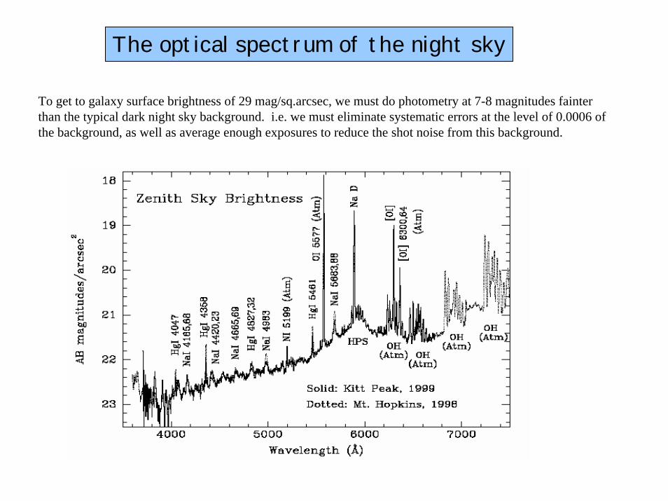
The optical spectrum of the night sky
To get to galaxy surface brightness of 29 mag/sq.arcsec, we must do photometry at 7-8 magnitudes fainter than the typical dark night sky background. i.e. we must eliminate systematic errors at the level of 0.0006 of the background, as well as average enough exposures to reduce the shot noise from this background.

Front and back-illuminated CCDs
The fine surface electrode structure of a front-illuminated CCD is clearly visible as a multi-coloredinterference pattern. Backside Illuminated CCDs have a much planer surface appearance. The other notable distinction is the higher QE in the AR-coated chip on the right. At the level of a few parts per thousand (our science challenge) every CCD is unique, and the gain and other properties of every pixel must be understood in each exposure. Luckily, CCDs are linear over a wide range.
Frontside-illuminated CCD Backside-illuminated CCD

Slow Scan Frame Transfer CCDsA common science-grade design uses 2 serial registers and 4 output amplifiers. Extra clocklines are required to divide the image area into an upper and lower section. Further clock lines allow independent operation of each half of each serial register. It is thus possible to read out theimage in four quadrants simultaneously, reducing the readout speed by a factor of four.
Upper Image area clocks
Lower Image area clocks
Amplifier C
Amplifier A Amplifier B
Amplifier D
Serial clocks C Serial clocks D
Serial clocks A Serial clocks B

Dynamic Range and A/D Conversion
DYNAMIC RANGE: The useful range of charge per pixel (at the input of the sense node amplifier is set by the read noise per pixel of this amplifier and the number of electrons per pixel in the brightest object in the exposure. For CCDs with 10-15 micron pixels and good MOSFET amplifiers this dynamic range can be from 3 – 200,000 electrons, a factor of 67,000! This can span the noise in a shutter closed “zero” frame to a time exposure with sky background plus stars and galaxies. Far better than the factor of 50 in photography.
ANALOG TO DIGITAL CONVERSION: We must convert the corresponding voltage output of this on-chip amplifier to digital data. This is done with some more amplification followed by an A/D converter. A 16-bit A/D has a range of 65,000. We want the least significant bit to measure the lowest noise level expected (shutter closed): the read noise.There are half a dozen ways to do this. Here are a couple: the parallel encoder flash A/D and the delta-sigma charge-balancing A/D. Pixel conversion times must be ~1 microsecond!
Noise Sources in a CCD Image
The main noise sources found in a CCD are :
1. READ NOISE.Caused by electronic noise in the CCD output transistor and possibly also in the external circuitry.Read noise places a fundamental limit on the performance of a CCD. It can be reduced at the expense of increased read out time. Scientific CCDs have a readout noise of 2-3 electrons RMS.
2. DARK CURRENT.Caused by thermally generated electrons in the CCD. Eliminated by cooling the CCD.
3. PHOTON NOISE.Also called ‘Shot Noise’. Photons arrive in a random fashion described by Poisson statistics.
4. PIXEL RESPONSE NON-UNIFORMITY.Defects in the silicon and small manufacturing defects can cause some pixels to have a higher sensitivity than their neighbours. This “noise” source can be removed by ‘Flat Fielding’; an image processing technique.

Noise Sources in a CCD Image
Before these noise sources are explained further some new terms need to be introduced.
FLAT FIELDINGThis involves exposing the CCD to a very uniform light source that produces a featureless and evenexposure across the full area of the chip. A flat field image can be obtained by exposing on a twilight sky or on an illuminated white surface held close to the telescope aperture (for example the inside of the dome). Flat field exposures are essential for the reduction of astronomical data.
BIAS OVERSCAN REGIONSA bias region is an area of a CCD that is not sensitive to light. The value of pixels in a bias region is determined by the signal processing electronics. It constitutes the zero-signal level of the CCD.The bias region pixels are subject only to readout noise. Bias regions can be produced by ‘over-scanning’ a CCD, i.e. reading out more pixels than are actually present. Designing a CCD witha serial register longer than the width of the image area will also create vertical bias strips at the leftand right sides of the image. These strips are known as the ‘x-underscan’ and ‘x-overscan’ regions
A flat field image containing bias regions can yield valuable information not only on the variousnoise sources present in the CCD but also about the gain of the signal processing electronicsi.e. the number of photoelectrons represented by each digital unit (ADU) output by the camera’sAnalog to Digital Converter.

Bias Overscan RegionsFlat field images obtained from two CCD geometries are represented below. The arrows representthe position of the readout amplifier and the thick black line at the bottom of each image represents the serial register.
CCD With SerialRegister equal inlength to the image area width.
Image Area
CCD With SerialRegister greater inlength than the image area width.
Image Area
X-o
vers
can
Y-overscan
Here, the CCD is over-scanned in X and Y
X-o
vers
can
X-u
nder
scan
Y-overscan Here, the CCD is over-scanned in Yto produce the Y-overscan bias area.The X-underscan and X-overscan are created by extensions to the serial register on either side of the image area. When charge is transferred from the image area into the serial register, these extensionsdo not receive any photo-charge.

CCD Read NoiseThese four noise sources are now explained in more detail:
READ NOISE.This is mainly caused by Johnson noise in the output amplifier. This noise source can be reduced by cooling the output amplifier or by decreasing its electronic bandwidth. Decreasing the bandwidth means that we must take longer to measure the charge in each pixel, so there is alwaysa trade-off between low noise performance and speed of readout. 60Hz pickup and interference from circuitry in the observatory can also contribute to Read Noise but can be eliminated by careful design.Johnson noise is more fundamental and is always present to some degree.
The graph below shows the trade-off between noise and readout speed for a CCD.
0
2
4
6
8
10
12
14
2 3 4 5 6
Time spent measuring each pixel (microseconds)
Read
Noi
se (e
lect
rons
RM
S)

CCD Dark Current NoiseDARK CURRENT.Electrons can be generated in a pixel either by thermal motion of the silicon atoms or by the absorptionof photons. Electrons produced by these two effects are indistinguishable. Dark current can be reduced or eliminated entirely by cooling the CCD. Science cameras are typically cooled with liquidnitrogen to the point where the dark current falls to below 1 electron per pixel per hour where it is essentially un-measurable. The graph below shows how the dark current of a CCD can be reduced by cooling.
1
10
100
1000
10000
-110 -100 -90 -80 -70 -60 -50 -40
Temperature Centigrade
Ele
ctro
ns p
er p
ixel
per
hou
r

Photon Shot Noise
PHOTON NOISE.Small pixels collect very low fluxes of photons.
Poisson statistics tells us that the Root Mean square uncertainty (RMS noise) in the number of photons per second detected by a pixel is equal to the square root of the mean photon flux (the average number of photons detected per second).For example, if a star is imaged onto a pixel and it produces on average 10 photo-electrons persecond and we observe the star for 1 second, then the uncertainty of our measurement of its brightnesswill be the square root of 10 i.e. 3.2 electrons. This value is the ‘Photon Noise’.Increasing exposure time to 100 seconds will increase the photon noise to 10 electrons (the square root of 100) but at the same time will increase the ‘Signal to Noise ratio’ (SNR). In the absence of other noise sources the SNR will increase as the square root of the exposure time.
( Dark current, described earlier, is also governed by Poisson statistics. If the mean dark current contribution to an image is 900 electrons per pixel, the noise introduced into the measurementof any pixel’s photo-charge would be 30 electrons )

Pixel QE or gain “noise”
PIXEL RESPONSE NON-UNIFORMITY.If we take a bright (at least 50,000 electrons of photo-generated charge per pixel) flat field exposure,the contribution of photon noise and read noise become very small. If we then plot the pixel values along a row of the image we see a variation in the signal caused by the slight variations in sensitivitybetween the pixels. The graph below shows this for a CCD illuminated by blue light. The variations are as much as +/-2%. Fortunately these sensitivity differences are constant and are easily removed by dividing a science image, pixel by pixel, by a flat field image.
-3
-2
-1
0
1
2
3
0 100 200 300 400 500 600 700 800
column number
% v
aria
tion
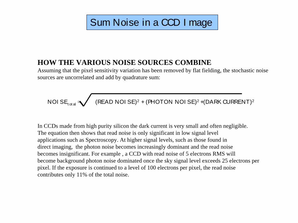
HOW THE VARIOUS NOISE SOURCES COMBINEAssuming that the pixel sensitivity variation has been removed by flat fielding, the stochastic noise sources are uncorrelated and add by quadrature sum:
In CCDs made from high purity silicon the dark current is very small and often negligible. The equation then shows that read noise is only significant in low signal levelapplications such as Spectroscopy. At higher signal levels, such as those found indirect imaging, the photon noise becomes increasingly dominant and the read noise becomes insignificant. For example , a CCD with read noise of 5 electrons RMS will become background photon noise dominated once the sky signal level exceeds 25 electrons per pixel. If the exposure is continued to a level of 100 electrons per pixel, the read noise contributes only 11% of the total noise.
Sum Noise in a CCD Image
NOISEtotal = (READ NOISE)2 + (PHOTON NOISE)2 +(DARK CURRENT)2

Measuring Read Noise: Photon Transfer Method
Using two identical flat field exposures it is possible to measure the read noiseof a CCD with the Photon Transfer method. Two exposures are required to removethe contribution of the pixel response variations and of small imperfections in the flat fields caused by uneven illumination.
The method actually measures the conversion gain of the CCD camera; the number of electrons represented by each digital interval (ADU) of the analog to digital converter, however, once the gain is known the read noise can be obtained directly.
This method exploits the Poisson statistics of photon arrival. To use it, one requires an image analysis program capable of doing statistical analysis on selected areas of the input images.
The read noise and the shot noise from a uniform exposure add inquadrature:
(Total Noise )2 = G2 * ReadNoise2 + G * ExposureLevel
where G = gain

Photon Transfer Method
Bias area 1Image area 1
Bias area 2Image area 2
STEP 1
Measure the Standard Deviation in the two bias areas and averagethe two values.Result = NoiseADU [the Root Mean Square readout noise in ADU]
STEP 2
Measure the mean pixel value in the two bias areas and the two image areas. Then subtract MeanBias area 1 from MeanImage area 1result= MeanADU [ the Mean Signal in ADU]
As an extra check repeat this for the second image, the Mean should be very similar. If it is more than a few percent different it may be best to take the two flat field exposures again.
Flat Field Image 2.
Flat Field Image 1.

Photon Transfer Method
Image area 3
STEP 4
Measure the Standard Deviation in image area 3result= StdDevADU .The statistical spread in the pixel values in this subtracted image area will be due to a combination of readout noise and photon noise.
STEP 5
Now get the gain via the following equation.
STEP 3 The two images are then subtracted pixel by pixel to yield a third image
Image 1 - Image 2 = Image 3
Gain = 2 x MeanADU
(StdDevADU ) 2 - (2 x NoiseADU2).
The units will be electrons per ADU, which will be inverselyproportional to the voltage gain of the system.

Photon Transfer Method
STEP 6 The Readout noise is then calculated using this gain value :
Readout Noiseelectrons= Gain x NoiseADU
Precautions when using this method
The exposure level in the two flat fields should be at least several thousand ADUbut not so high that the chip or the processing electronics is saturated. 10,000 ADUwould be ideal. It is best to average the gain values obtained from several pairsof flat fields. Alternatively the calculations can be calculated on several sub-regions of a single image pair. If the illumination of the flat fields is not particularly flat and the signal level varies appreciably across the sub-region on whichthe statistics are performed, this method can fail.

Since 1982 the read noise of CCDs has decreased by a factor of 100

pixe
l bo
unda
ry
Phot
ons
Blooming in a CCD
The charge capacity of a CCD pixel is limited, when a pixel is full the charge starts to leak intoadjacent pixels along a column. This process is known as ‘Blooming’.
Phot
onsOverflowing
charge packet
Spillage Spillage
pixe
l bo
unda
ry

Blooming in a CCD
The diagram shows one column of a CCD with an over-exposed stellar image focused on one pixel.
The channel stops shown in yellow prevent the chargespreading sideways along a row. The charge confinement providedby the electrodes is less so the charge spreads vertically upand down a column.
The capacity of a CCD pixel is known as the ‘Full Well’. It isdependent on the physical area of the pixel. For pixels measuring 20μm x 20μm it can be as much as 300,000 electrons. Bloomed images will be seen particularly on nights of good seeing where stellar images are more compact .
In reality, blooming is not a big problem for professionalastronomy.
Flow
of
bloo
med
ch
arge
Blooming in a CCD
Bloomed star images
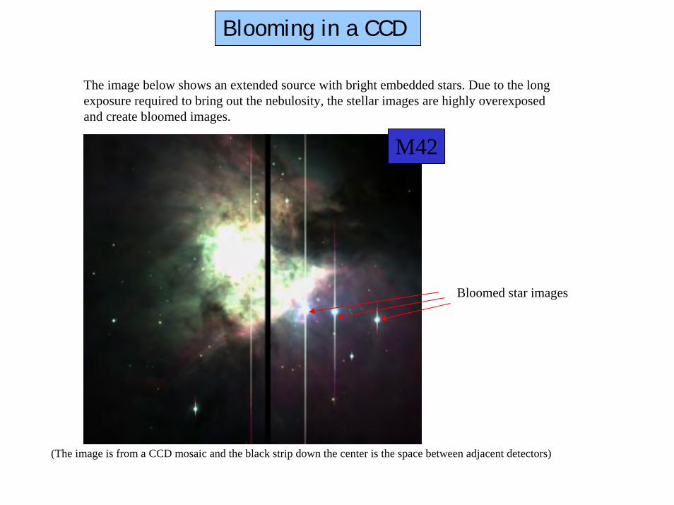
The image below shows an extended source with bright embedded stars. Due to the longexposure required to bring out the nebulosity, the stellar images are highly overexposedand create bloomed images.
(The image is from a CCD mosaic and the black strip down the center is the space between adjacent detectors)
M42

Modest beginnings: The first imaging CCD had large gain and CTE variations

Image Defects in a CCD
Unless one pays a huge amount it is generally difficult to obtain a CCD free of image defects. The first kind of defect is a ‘dark column’. Their locations are identified from flat field exposures.
Flat field exposure of an EEV42-80 CCD
Dark columns are caused by ‘traps’ that block the vertical transfer of charge during image readout. The CCD shown at left has at least 7 dark columns, some grouped together inadjacent clusters.
Traps can be caused by crystal boundaries in the silicon of the CCD, impurities, or by manufacturing defects.
Although they spoil the chip cosmetically, dark columns are not a big problem for astronomers. This chip has 2048 image columns so 7 bad columns represents a tiny loss of data.
CHARGE TRANSFER EFFICIENCY (CTE):A related systematic error is the tendency at low light levels for incomplete charge transfer. CTE of 0.999995 per pixel transfer is common at high levels, but at low levels traps can cause many small dark columns.

Image Defects in a CCD
Bright columns are also caused by traps . Electrons containedin such traps can leak out during readout causing a vertical streak.
Hot Spots are pixels with higher than normal dark current. Theirbrightness increases linearly with exposure times
Cosmic rays are unavoidable. Charged particles from space orfrom radioactive traces in the material of the camera cancause ionization in the silicon. The electrons produced areindistinguishable from photo-generated electrons. Approximately 2 cosmic rays per cm2 per minute will be seen.A typical event will be spread over a few adjacent pixels and contain several thousand electrons. But most are still more compact than the stellar point-spread function.
Somewhat rarer are light-emitting defects which are hot spots that act as tiny LEDS and cause a halo of light on the chip.
There are three other common image defect types : Cosmic rays, Bright columns and Hot Spots.Their locations are shown in the image below which is a lengthy exposure taken in the dark (a ‘Dark Frame’)
Cosmic rays
Cluster ofHot Spots
BrightColumn
900s dark exposure of an EEV42-80 CCD

Image Defects in a CCD
M51
Some defects can arise from the processing electronics. This negative image has a bright line in the first image row.
Dark column
Hot spots and bright columns
Bright first image row caused byincorrect operation of signalprocessing electronics.

Fringing in a CCD
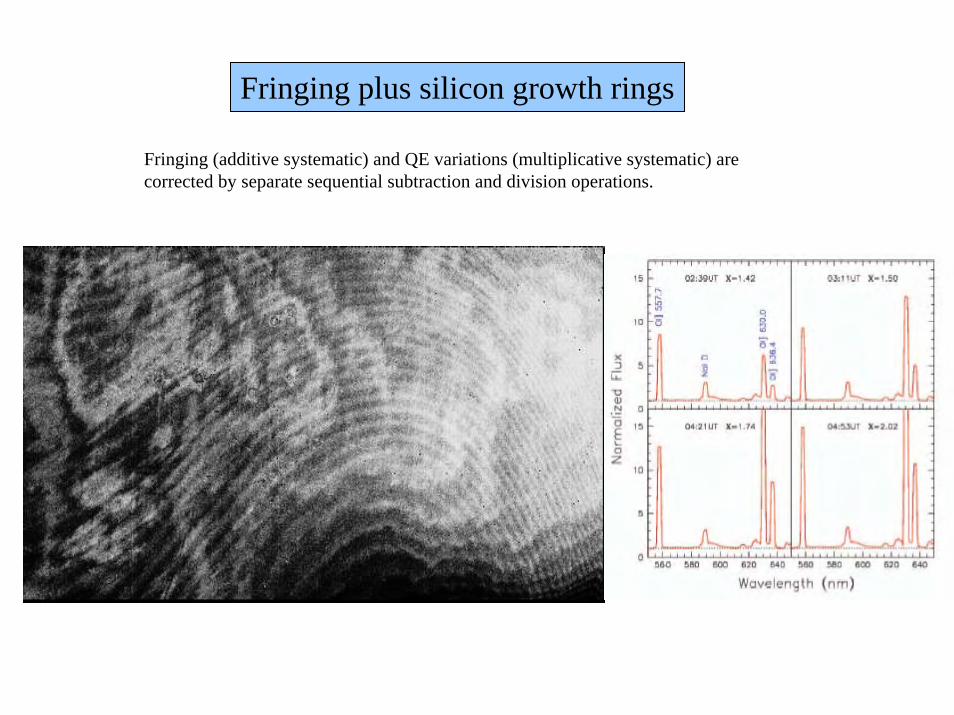
Fringing plus silicon growth rings
Fringing (additive systematic) and QE variations (multiplicative systematic) are corrected by separate sequential subtraction and division operations.

Biases, Flat Fields and Dark Frames
These are three types of calibration exposures that must be taken with a scientific CCD camera, generally before and after each observing session. They are stored alongside the science imagesand combined with them during image processing. These calibration exposures allow us to compensate forimperfections in the CCD. As much care needs to be exercised in obtaining these images as forthe actual scientific exposures. Applying low quality flat fields and bias frames to scientific data can degrade rather than improve its quality.
Bias FramesA bias frame is an exposure of zero duration taken with the camera shutter closed. It represents the zero point or base-line signal from the CCD. Rather than being completely flat and featureless the bias framemay contain some structure. Any bright image defects in the CCD will of course show up, there may be
also slight gradients in the image caused by limitations in the signal processing electronics of the camera. It is normal to take about 20 bias frames before a night’s observing. These are then combined using an image processing algorithm that averages the images, pixel by pixel, rejecting any pixel values that are appreciably different from the other 19. This can happen if a pixel in one bias frame is affected by a cosmic ray event. It is unlikely that the same pixel in the other 19 frames would be similarly affected so the resultant ‘master bias’,should be uncontaminated by cosmic rays. Taking a number of biases and then averaging them also reducesthe amount of noise in the bias images. Averaging 25 frames will reduce the amount of read noise (electronic noise from the CCD amplifier) in the image by a factor of 5.
Biases, Flat Fields and Dark Frames
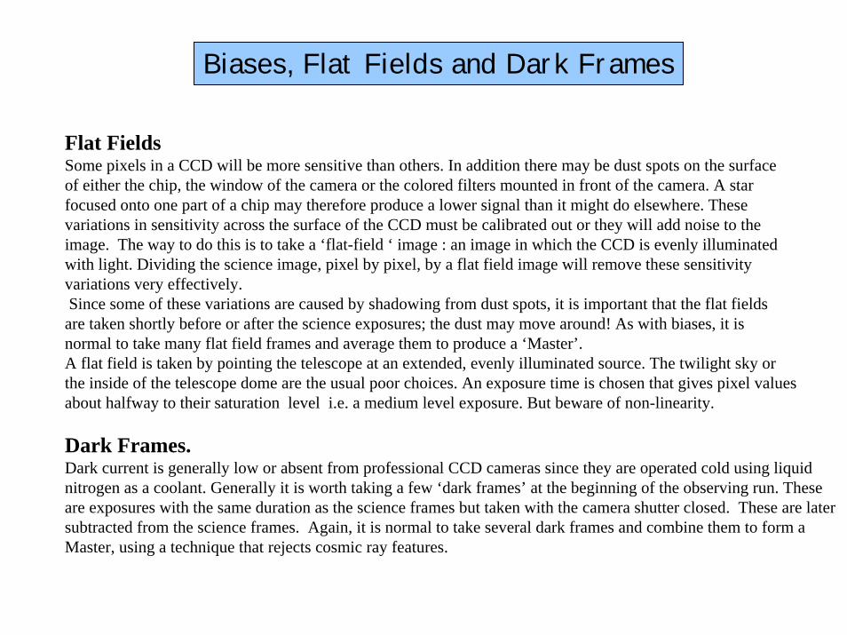
Flat FieldsSome pixels in a CCD will be more sensitive than others. In addition there may be dust spots on the surfaceof either the chip, the window of the camera or the colored filters mounted in front of the camera. A star focused onto one part of a chip may therefore produce a lower signal than it might do elsewhere. These variations in sensitivity across the surface of the CCD must be calibrated out or they will add noise to the image. The way to do this is to take a ‘flat-field ‘ image : an image in which the CCD is evenly illuminated with light. Dividing the science image, pixel by pixel, by a flat field image will remove these sensitivityvariations very effectively. Since some of these variations are caused by shadowing from dust spots, it is important that the flat fields are taken shortly before or after the science exposures; the dust may move around! As with biases, it is normal to take many flat field frames and average them to produce a ‘Master’.A flat field is taken by pointing the telescope at an extended, evenly illuminated source. The twilight sky orthe inside of the telescope dome are the usual poor choices. An exposure time is chosen that gives pixel values about halfway to their saturation level i.e. a medium level exposure. But beware of non-linearity.
Dark Frames.Dark current is generally low or absent from professional CCD cameras since they are operated cold using liquid nitrogen as a coolant. Generally it is worth taking a few ‘dark frames’ at the beginning of the observing run. These are exposures with the same duration as the science frames but taken with the camera shutter closed. These are later subtracted from the science frames. Again, it is normal to take several dark frames and combine them to form a Master, using a technique that rejects cosmic ray features.

Dark Frame Flat Field
A dark frame and a flat field from the same CCD are shown below. The dark frame shows a number of bright defects on the chip. The flat field shows a criss-cross patterning on the chip created during manufacture and a slight loss of sensitivity in two corners of the image. Some dustspots are also visible.
Biases, Flat Fields and Dark Frames

Flat Field Image
Bias Image
Flat-Bias
Science -Dark
Output Image
Flat-BiasScience -Dark
Dark Frame
Science Frame
Biases, Flat Fields and Dark Frames If there is significant dark current present, the various calibration and science framesare combined by the following series of subtractions and divisions :
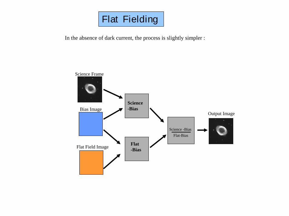
Flat Fielding
Flat Field Image
Bias Image
Flat-Bias
Science -Bias
Output Image
Flat-BiasScience -Bias
Science Frame
In the absence of dark current, the process is slightly simpler :

RawBias

Raw DomeFlat
DomeFlatcorrected
Pixel Size and Binning
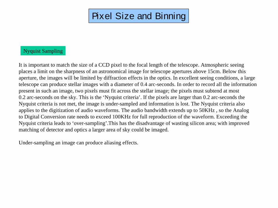
It is important to match the size of a CCD pixel to the focal length of the telescope. Atmospheric seeingplaces a limit on the sharpness of an astronomical image for telescope apertures above 15cm. Below this aperture, the images will be limited by diffraction effects in the optics. In excellent seeing conditions, a large telescope can produce stellar images with a diameter of 0.4 arc-seconds. In order to record all the information present in such an image, two pixels must fit across the stellar image; the pixels must subtend at most 0.2 arc-seconds on the sky. This is the ‘Nyquist criteria’. If the pixels are larger than 0.2 arc-seconds the Nyquist criteria is not met, the image is under-sampled and information is lost. The Nyquist criteria also applies to the digitization of audio waveforms. The audio bandwidth extends up to 50KHz , so the Analog to Digital Conversion rate needs to exceed 100KHz for full reproduction of the waveform. Exceeding the Nyquist criteria leads to ‘over-sampling’.This has the disadvantage of wasting silicon area; with improved matching of detector and optics a larger area of sky could be imaged.
Under-sampling an image can produce aliasing effects.
Nyquist Sampling

Pixel Size and Telescope
Example The Blanco Telescope, with a 4m diameter primary mirror and a focal ratio of 2.7 is to be usedfor prime focus imaging. What is the optimum pixel size assuming that the best seeing at the telescope siteis 0.7 arc-seconds ?First we calculate the ‘plate-scale’ in arc-seconds per millimeter at the focal plane of the telescope.
Plate Scale (arc-seconds per mm) = = 19.1 arc-sec per mm
(here the factor 206265 is the number of arc-seconds in a Radian )
Next we calculate the linear size at the telescope focal plane of a stellar image (in best seeing conditions)
Linear size of stellar image = 0.7 arcsec / Plate Scale = 0.7/ 19.1 = 37 microns.
To satisfy the Nyquist criteria, the maximum pixel size is therefore 18 microns. In practice, the nearestpixel size available is 15 microns which leads to a small degree of over-sampling.
Matching the Pixels to the telescope
206265
Aperture in mm X f-number

Controlling the CCD Clocks
Computers are required firstly to coordinate the sequence of clock signals that need to be sent to a CCDand its signal processing electronics during the readout phase, but also for data collection and the subsequent processing of the images.
The CCD ControllerIn this first application, the computer is an embedded system running in a ‘CCD controller’. This controller willtypically contain a low noise analog section for amplification and filtering of the CCD video waveform,an analog to digital converter, a high speed processor for clock waveform generation and a fibre optic transceiver for receipt of commands and transmission of pixel data. An astronomical system might require clock signals to be generated with time resolutions of a few tens of nanoseconds. This is typically done using Digital Signal Processing (DSP) chips running at 50Mhz. Clocksequences are generated in software and output from the DSP by way of on-chip parallel ports. The most basic CCD design requires a minimum of 7 clock signals. Perhaps 5 more are required to coordinate the operation of the signal processing electronics. DSPs also contain several on-chip serial portswhich can be used to transmit pixel data at very high rates. DSPs come with a small on-chip memory for the storage of waveform generation tables and software. Less time critical code , such as routines to initialise the camera and interpret commands can be stored in a few KB of external RAM. The computerrunning in the CCD controller is thus fast and of relatively simple design. A poorly performing processor herecould result in slow read out times and poor use of telescope resources. Remember that when a CCD is readingout the telescope shutter is closed and no observations are possible.

Mosaic Cameras
The pictures below show the galaxy M51 and the CCD mosaic that produced the image.Two EEV42-80 CCDs are screwed down onto a very flat Invar plate with a 50 micron gapbetween them. Light falling down this gap is obviously lost and causes the black stripdown the centre of the image. This loss is not of great concern to astronomers, since it represents only 1% of the total data in the image.

Mosaic Cameras
Another image from this camera is shown below. The object is M42 in Orion.This false color image covers an area of sky measuring 16’ x 16’.

Mosaic Cameras
A further image is shown below, of the galaxy M33 in Triangulum. Images from this camera are enormous; each of the two chips measures 2048 x 4100 pixels. The original images occupy 32MB each.

Mosaic Cameras
The Horsehead Nebula in Orion. The mosaic mounted in its camera.

Mosaic Cameras 6.
This mosaic of 12 CCDs is in operation at the CFHT in Hawaii. Here is an example of what it can produce. The chips are of fairly low cosmetic quality.

Mosaic Cameras This mosaic of 8 science CCDs was built for the NOAO 4-meter telescopes.

Camera Construction Techniques
The main body of the camera is a 3mm thick aluminium pressure vessel able to supportan internal vacuum. Most of the internal volume is occupied by a 2.5 liter copper can that holds liquid nitrogen (LN2). The internal surfaces of the pressure vessel and the externalsurfaces of the copper can are covered in aluminized mylar film to improve the thermal isolation. As the LN2 boils off , the gas exits through the same tube that is used forthe initial fill
The CCD is mounted onto a copper cold block that is stood-off from the removable end plate by thermally insulating pillars. A flexible copper braid connects this block to the LN2can. The thickness of the braid is adjusted so that the equilibrium temperature of the CCD is about 10 degrees below the optimum operating temperature. The mountingblock also contains a heater resistor and a Platinum resistance thermometer that are used to servo the CCD temperature. Without using a heater resistor close to the chip for thermal regulation , the operating temperature and the CCD characteristics also, will vary with the ambient temperature.
The removable end plate seals with a synthetic rubber ‘o’ ring. In its centeris a fused silica window big enough for the CCD and thick enough to withstand atmosphericpressure. The CCD is positioned a short distance behind the window and radiatively cools the window. To prevent condensation it is necessary to blow dry air across the outside.

Camera Construction Techniques
The basic structure of the camera is that of a Thermos flask. Its function is to protect the CCD in a cold clean vacuum. The thermal design is very important, so as to maximize the hold time and the time between LN2 fills. Maintenance of a good vacuum is alsovery important, firstly to improve the thermal isolation of the cold components but also toprevent contamination of the CCD surface. A cold CCD is very prone to contamination fromvolatile substances such as certain types of plastic. These out-gas into the vacuum spaces of the camera and then condense on the coldest surfaces. This is generally the LN2 can. On the back of the can is a small container filled with activated charcoal known as a ‘Getter’.This acts as a sponge for any residual gases in the camera vacuum. The getter contains a heater to drive off the absorbed gases when the camera is being pumped.
This camera is vacuum pumped for several hours before it is cooled down. The pressure at the end of the pumping period is about 10-4 mBar. When the LN2 is introduced, the pressure willfall to about 10-6mBar as the residual gases condense out on the LN2 can.
When used in an orientation that allows this camera to be fully loaded with LN2, the boil off or ‘hold time’ is about 20 hours. The thermal energy absorbed by 1g of LN2 turning to vapor is 208J, the density of LN2 is 0.8g/cc. From this we can calculate that the heat load on the LN2 can, from radiation and conduction is about 6W.

Camera Construction Techniques
. . .
A cutaway diagram of a typical camera is shown below.
Thermally Electrical feed-through Vacuum Space Pressure vessel Pump PortInsulatingPillars
Foca
l Pla
ne
of T
eles
cope
Tele
scop
e be
am
Optical window CCD CCD Mounting Block Thermal coupling Nitrogen can Activated charcoal ‘Getter’
Boil-off
Face-plate

Camera Construction Techniques
CCDTemperature servo circuit board
Gold plated copper mounting block
Top of LN2can
PressureVessel
Signal wires to CCDLocation points (x3)for insulating pillarsthat reference the CCDto the camera face-plate
Platinum resistancethermometer
Aluminised Mylarsheet
Retainingclamp
The camera with the face-plate removed is shown below
‘Spider’.The CCD mountingblock is stood off from the spider usinginsulating pillars.


![Aural landscapes: Designing a sound environment for screen ... · As David Sonnenschein states, “[by] giving meaning to noise, sound becomes communication” (2001, p. xix). Through](https://static.documents.pub/doc/80x56/60b65267106d3339905b61d2/aural-landscapes-designing-a-sound-environment-for-screen-as-david-sonnenschein.jpg)


