1 EX/P5-08 Impact of Arcing on Carbon and Tungsten: from the Observations in JT-60U, LHD, and NAGDIS-II Shin Kajita 1 , Masakatsu Fukumoto 2 , Masayuki Tokitani 3 , Tomohide Nakano 2 , Suguru Masuzaki 3 , Noriyasu Ohno 4 , Shuichi Takamura 5 , Naoaki Yoshida 6 and Yoshio Ueda 7 1 EcoTopia Science Institute, Nagoya University, Furo-cho, Chikusa, Nagoya 464-8603, Japan 2 Japan Atomic Energy Agency, Ibaraki 801-1, Japan 3 National Institute for Fusion Science, 322-6 Oroshi, Toki, Gifu 509-5292, Japan 4 Graduate School of Engineering, Nagoya University, Furo-cho,Chikusa, Nagoya 464-8603, Japan 5 Aichi Institute of Technology, Toyota 470-0392, Japan 6 Research Institute for Applied Mechanics, Kyushu University, Fukuoka 816-8580, Japan 7 Graduate School of Engineering, Osaka University, Suita, Osaka 565-0871, Japan Corresponding Author: [email protected]Abstract: This paper assesses the impact of arcing in fusion devices based on the observations in JT- 60U, LHD, and the linear divertor simulator NAGDIS-II. In NAGDIS-II, the demonstration experiments of arcing/unipolar arcing have been conducted by simulating the transient heat load using a pulsed laser; it was found that the arcing can be easily initiated on the helium irradiated nanostructured tungsten. By measuring the field emission current property from the helium irradiated tungsten surface, the initiation conditions are discussed. From the detailed analysis of JT-60U tiles, it is found that arcing phenomena occurred on carbon baffle plates. From the observation of the arc trails recorded on the baffle plate, the amount of the eroded materials is discussed. The arcing seemed to occur frequently on inner baffles rather than the outer baffles. From LHD, it is shown that the arcing can be initiated on nanostructured tungsten even without transient events. The erosion of tungsten by arcing will become an important issue in a fusion reactor, where helium fluence is significantly increased. 1 Introduction Arcing in fusion devices had been extensively investigated from 1970’s [1, 2]. Since arcing can be an impurity sources, there is a concern that the core performance could be dete- riorated if arcing would occur frequently. Federici et al. pointed out that arcing may be
Transcript
1 EX/P5-08
Impact of Arcing on Carbon and Tungsten:from the Observations in JT-60U, LHD, and
1EcoTopia Science Institute, Nagoya University, Furo-cho, Chikusa, Nagoya 464-8603,Japan2Japan Atomic Energy Agency, Ibaraki 801-1, Japan3National Institute for Fusion Science, 322-6 Oroshi, Toki, Gifu 509-5292, Japan4Graduate School of Engineering, Nagoya University, Furo-cho,Chikusa, Nagoya 464-8603,Japan5Aichi Institute of Technology, Toyota 470-0392, Japan6Research Institute for Applied Mechanics, Kyushu University, Fukuoka 816-8580, Japan7Graduate School of Engineering, Osaka University, Suita, Osaka 565-0871, Japan
Abstract:This paper assesses the impact of arcing in fusion devices based on the observations in JT-60U, LHD, and the linear divertor simulator NAGDIS-II. In NAGDIS-II, the demonstrationexperiments of arcing/unipolar arcing have been conducted by simulating the transient heatload using a pulsed laser; it was found that the arcing can be easily initiated on the heliumirradiated nanostructured tungsten. By measuring the field emission current property fromthe helium irradiated tungsten surface, the initiation conditions are discussed. From thedetailed analysis of JT-60U tiles, it is found that arcing phenomena occurred on carbonbaffle plates. From the observation of the arc trails recorded on the baffle plate, the amountof the eroded materials is discussed. The arcing seemed to occur frequently on inner bafflesrather than the outer baffles. From LHD, it is shown that the arcing can be initiated onnanostructured tungsten even without transient events. The erosion of tungsten by arcingwill become an important issue in a fusion reactor, where helium fluence is significantlyincreased.
1 Introduction
Arcing in fusion devices had been extensively investigated from 1970’s [1, 2]. Since arcingcan be an impurity sources, there is a concern that the core performance could be dete-riorated if arcing would occur frequently. Federici et al. pointed out that arcing may be
EX/P5-08 2
important in the divertor, but the insufficient data from current tokamaks exist to reli-ably extrapolate to an ITER class device [3]. Recently, the arcing issue has been broughtabout from new points[4, 5]: one is the transients accompanied with edge localized modes(ELMs) and the other is the surface morphology change, especially nanostructurization,by plasma irradiation. That is the perturbations in plasmas and surface smoothness canenhance the initiation of arcing. Indeed, arcing has been recently reported from ASDEXUpgrade [6, 7], where arcings were initiated on tungsten, probably in response to ELMs.The arcing has been observed
To understand the impact of arcing in fusion devices, it is necessary to assess theerosion of material by arcing, since the estimation is difficult at present because of thelack of experimental data [3]. Thus, it is of important to collect the information of arcingin the present tokamak devices. Moreover, it is necessary to understand the initiationconditions of arcing from the plasma side and material side. In this paper, the impact ofarcing in fusion devices is discussed based on the experimental observations in a lineardevice, JT-60U, and LHD.
2 Initiation of Arcing
20
15
10
5
0
Cu
rre
nt
de
ns
ity
[µ
A/m
m2]
6050403020100
Electric field [V/µm]
Nanostructure
Virgin
-12
-10
-8
-6
-4
ln (
J/E
2)
8x10⁻²
6420
1/E
Nanostructure
Virgin
FIG. 1: Field electron emission current as a function of the applied electric field strengthfrom a nanostructured tungsten and polished bulk tungsten. Inset shows the FN plot.
The initiation condition and behavior of arc spot was demonstrated in detail in thelinear divertor simulator NAGDIS-II [8, 9]. In future fusion devices including ITER,materials are exposed to helium ions. Thus, in NAGDIS-II, the nanostructure tungstenexposed to helium plasma was used for the experiments. A pulsed laser (λ=694.7 nm)was used to mimic the transient heat load while the sample was exposed to the heliumplasma. The pulse width was ∼0.5 ms, which was similar to the Type-I ELMs. Fromthe experiments in NAGDIS-II, the necessary averaged laser pulse energy to ignite arcingwas approximately 0.01 MJm−2 [8] when the nanostructure was formed on the surface bythe helium plasma irradiation. Even taking into account the spikes of the laser pulse, the
3 EX/P5-08
necessary energy to ignite arcing seemed more than one order of magnitude lower thanthe mitigated type-I ELMs in ITER such as 0.5 MJm−2. Thus, it raises a concern that thearcing is also triggered by small plasma heat load due to the type-II or type-III ELMs inITER if the nanostructures are formed on the surface. Moreover, after the nanostructurewas formed on the surface, the arcing was initiated even when the electron density waslower than 1017 m−3.
An electron emission process is thought to be important on the initiation of arcing.The emission process is thermo-field emission in which thermionic emission was correctedby including the Schottky effect. To investigate the properties of the electron emissionprocess, field emission from the nanostructured tungsten was measured. Figure 1 showsthe electron current as a function of the applied electric field strength from a nanostruc-tured tungsten and polished bulk tungsten. The experiments were conducted in vacuumwith the background pressure of ∼10−4 Pa. The nanostructured tungsten was formed inthe linear plasma device NAGDIS-II. The irradiation was conducted with the ion energyof ∼ 60 eV, the surface temperature of 1500 K, and the helium fluence of 2.2 ×1025 m−2.The nanostructure was fully developed on the surface. For the nanostructured tungsten,the current increased significantly around the field strength of 20 V/µm. The turn onvoltage was ∼ 15 V/µm. It is seen that the field emission current from the nanostruc-tured tungsten is significantly greater than that from a polished bulk tungsten surface.The Fowler-Nordheim (FN) plot of the relation between the current and field strengthis shown in the inset of Fig. 1. The field enhancement factor can be obtained from theslope of the plot [10]. The field enhancement factor was estimated to be ∼200 for thenanostructured tungsten. The value is not so high compared with the bulk materials,which is usually 50–100 [11]. Thus, the increase in the current indicated the increase inthe effective emission area.
Thermo-field emission current was theoretically investigated in [12], and the currentdensity can be calculated with the field strength, surface temperature, and work function.The calculation included a slightly complicated integral process and simplified approxi-mation have been proposed [13]; in this paper, the field strength is calculated from theoriginal equation in [12]. The field strength in front of the surface is determined by thesheath. The field strength is calculated by using the Poisson equation with the input pa-rameters of current density and the temperature of the plasma. In Fig. 2(a) and (b), thethermo-field emission current is plotted as a function of the plasma density and surfacetemperature. The work function was assumed to be that of the bulk tungsten of 4.5 eV.The electron temperature and ion temperature are assumed to be the same and 1 eV in(a) and 30 eV in (b). The field enhancement factor was assumed to be 200; the currentdensity is the local current density where field emission can easily occur. When the tem-perature is 30 eV, the current density becomes 107 A/m2 at the density of 1020 m−3 evenwhen the surface temperature is lower than 1000 K. The current density is comparableto the thermo electron emission around the melting point. When the density is 1021 atthe temperature of 30 eV, the current density exceeds 1013 which is six order greater thanthat at the density of 1020 m−3.
When the material is subjected to the plasma accompanied with ELMs, it is specu-lated that the density can exceed 1021 m−3 and the temperature is not so low, say higher
EX/P5-08 4
1019
2
4
6
810
20
2
4
6
810
21
2
4
6
810
22
1019
2
4
6
810
20
2
4
6
810
21
2
4
6
810
22 12 11
10 9 8
7 6
5 4
3 2 1
4000350030002500200015001000500
14
13
12
11
10 9
8 7
6 5
4 3 2 1
14121086420
Log (Current density [A/m2])
Surface temperature [K]
4000350030002500200015001000500
Surface temperature [K]E
lec
tro
n d
en
sit
y [
m-3
]
Ele
ctr
on
de
ns
ity
[m
-3]
Te=30 eVTe=1 eV
(a) (b)
FIG. 2: The thermo-field emission current is plotted as a function of the plasma densityand surface temperature. The work function was assumed to be that of the bulk tungstenof 4.5 eV. The electron temperature and ion temperature are assumed to be (a) 1 eV and(b) 30 eV. The field enhancement factor was assumed to be 200.
than 10 eV. Moreover, when the material is subjected to the transient heat load, thesurface temperature can rise correspondingly. When the nanostructure is formed on thesurface, an abnormal surface temperature rise can occur [14], because the surface diffusiv-ity near the surface decrease significantly. The increase in the surface temperature mayalso contribute to the increase in the thermo-field electron emission. Such a great currentcan lead to explosive electron emission process and trigger arcing [15].
3 Observation of arc trails in JT-60U
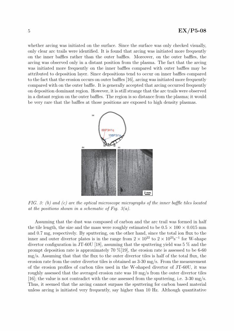
Figure 3(b) and (c) optical microscope micrographs of the inner baffle tiles located at thepositions shown in a schematic of Fig. 3(a). It was found that there are many trails thatalways run vertical direction, which is perpendicular to the magnetic field. The width ofthe trails is different from place to place, and the width seems greater than 1 mm in somepart.
Figure 4(a) and (b) shows a laser scanning microscope micrograph of the baffle tileof JT-60U. (a) is the image and (b) is the depth profile at the same position. It is seenthat the roughness is enhanced on the arc trail and the depth becomes deep, say severaltens of micrometer, in some positions. In Fig. 4(c) and (d), the depth profile indicatedas lines in Fig. 4, are presented. From the depth profile shown in Fig. 4(c), it is foundthat eroded depth is several tens of micrometers in some parts, where the deposited layerseemed to be peeled off. On the other hand, without peeling off, the erosion did not seemsignificant, though the surface roughness was enhanced by the arcing, as seen in Fig. 4(d).
All the baffle tiles of one toroidal section (∼ 20◦) was observed visually and investigated
5 EX/P5-08
whether arcing was initiated on the surface. Since the surface was only checked visually,only clear arc trails were identified. It is found that arcing was initiated more frequentlyon the inner baffles rather than the outer baffles. Moreover, on the outer baffles, thearcing was observed only in a distant position from the plasma. The fact that the arcingwas initiated more frequently on the inner baffles compared with outer baffles may beattributed to deposition layer. Since depositions tend to occur on inner baffles comparedto the fact that the erosion occurs on outer baffles [16], arcing was initiated more frequentlycompared with on the outer baffle. It is generally accepted that arcing occurred frequentlyon deposition dominant region. However, it is still strange that the arc trails were observedin a distant region on the outer baffles. The region is so distance from the plasma; it wouldbe very rare that the baffles at those positions are exposed to high density plasmas.
2 mm
(a)
(b) (c)
FIG. 3: (b) and (c) are the optical microscope micrographs of the inner baffle tiles locatedat the positions shown in a schematic of Fig. 3(a).
Assuming that the dust was composed of carbon and the arc trail was formed in halfthe tile length, the size and the mass were roughly estimated to be 0.5 × 100 × 0.015 mmand 0.7 mg, respectively. By sputtering, on the other hand, since the total ion flux to theinner and outer divertor plates is in the range from 2 × 10²² to 2 × 10²³s−1 for W-shapedivertor configuration in JT-60U [18], assuming that the sputtering yield was 5 % and theprompt deposition rate is approximately 70 %[19], the erosion rate is assessed to be 6-60mg/s. Assuming that that the flux to the outer divertor tiles is half of the total flux, theerosion rate from the outer divertor tiles is obtained as 3-30 mg/s. From the measurementof the erosion profiles of carbon tiles used in the W-shaped divertor of JT-60U, it wasroughly assessed that the averaged erosion rate was 10 mg/s from the outer divertor tiles[16]; the value is not contradict with the one assessed from the sputtering, i.e. 3-30 mg/s.Thus, it seemed that the arcing cannot surpass the sputtering for carbon based materialunless arcing is initiated very frequently, say higher than 10 Hz. Although quantitative
EX/P5-08 6
investigation is difficult at present, from the visual observation of the arc trails on thebaffles, it is unlikely that the arcing was initiated so frequently in JT-60U.
1 mm
[
(a) (b)
Depth
µm]
De
pth
[µ
m]
De
pth
[µ
m]
on arc trail
0
-10
-20
-30
-40
-50
0
-10
-20
-30
-40
-506420
Distance [mm]
17.2 µm13.1 µm
in (c)
in (d)
(c)
(d)
0
-10
-20
-30
-40
-50
toroidal direction
FIG. 4: (a) A laser scanning microscope micrograph of carbon baffle plate of JT-60U. (b)The depth profile of the surface measured by the laser scanning microscope.
4 Initiation of arcing in LHD
The nanostructured tungsten, which was fabricated in NAGDIS, was exposed to the LHDdivertor plasma for 2 s. After the exposure to the LHD plasma, interestingly, the arcingwas initiated even without any transient events, supporting the view that the arcing iseasily initiated on the nanostructured tungsten surface. In Fig 5(a), the white area inthe picture of the sample after the experiment indicates the area where arc spots runon the surface. Because the magnetic field direction was special and almost normal tothe surface, the spot moves freely without feeling the magnetic field effect; the fractalitymeasured using a box-counting method was almost two, indicating that the motion wassimilar to the Brownian motion. From the number of white area in Fig. 5(a), roughly, 25
Figure 5(b) shows the depth profile measured with a laser scanning microscope. It isseen that the eroded depth is approximately 1 µm, and the width of the trail is slightly lessthan 10 µ. From a mass loss measurement by Nishijima et al. [20], it was estimated thatthe porosity was approximately 0.9 when the thickness of the nanostructured layer is 1 µm.In addition, from the arc trail analysis using transmission electron microscopy (TEM),it was found that roughly half the nanostructured tungsten layer was still remained onthe surface for single spot arc trail [8]. Summarizing these, it is estimated that 150 µg oftungsten was roughly released by arcing from the nanostructured layer. Compared withthe erosion of carbon based material in JT-60U, the eroded amount is less; however, theimpact should be greater considering the fact that the permissible amount of tungsten inthe core is much less than that of carbon. In the present situation, the arc spot movesrandomly free of influence from the magnetic field. The arc spot will move linearly and
7 EX/P5-08
be terminated at the edge of the plate when the plate is not normal to the magnetic field.For future work, it is of interest to conduct arc experiments in the similar situation butthe magnetic field line is obliquely hit the plate.
1.0 mm
3
2
1
0D
ep
th [µ
m]
20151050
Distance [µm]
(b)(a)
50 µm
FIG. 5: (a) A optical microscope image exposed to the LHD plasma. (b) A depth profileof arc trail measured with a laser scanning microscope.
5 Conclusions
In this study, the arcing issue in nuclear fusion devices is presented from the linear plasmadevice NAGDIS-II, JT-60U, and LHD. From NAGDIS-II, the initiation process was inves-tigated in terms of the electron field emission. It was found that the electron field emissionincreases as changing the morphology by a helium plasma irradiation. Even though thefield enhancement factor is not much increased, the increase in the field emission currentshould increase the probability to initiate arcing.
From the laser scanning microscope observation of the arc trails recorded on JT-60Utiles, the amount of the erosion by arcing was estimated and compared with the erosionby sputtering. Since the erosion occurred from the deposited layer, which is composedof primarily carbon, it is thought that the arcing cannot be surpass the sputtering if thearcing occurs frequently, say like 10 Hz. Thus, it is said that, in JT-60U, erosion by arcinghad a minor effects.
From LHD, the arcing was initiated on nanostructured tungsten even without transientevents. It is estimated that 150 µg of tungsten was roughly released by arcing from thenanostructured layer. In future fusion reactors, since the helium fluence to tungsten issignificantly increased, the nanostructures can be formed on the surface. As we pointedout in this work, arcing can be initiated frequently without large transient events on thenanostructured surface; the erosion of tungsten by arcing becomes an important issue.
References
[1] G. McCracken and D. Goodall, Nucl. Fusion 18, 537 (1978).
EX/P5-08 8
[2] R. Behrisch, Physics of Plasma-Wall Interactions in Controlled Fusion (Nato ASISeries, Series B, Physics) (Plenum Pub. Corp., 1986) pp. 495–513.
[3] G. Federici, C. Skinner, J. Brooks, et al., Nucl. Fusion 41, 1967 (2001).
[4] M. Laux, W. Schneider, et al., IEEE Transactions on Plasma Science 33, 1470 (2005).
[5] S. Kajita, N. Ohno and S. Takamura, J. Nucl. Mater. 417, 838 (2011).
[6] A. Herrmann, M. Balden, et al., J. Nucl. Mater. 390-391, 747 (2009).
[7] V. Rohde, N. Endstrasser, et al., J. Nucl. Mater. 415, S46 (2011).
[8] S. Kajita, N. Ohno, et al., Plasma Phys. Control. Fusion 54, 035009 (2012).
[9] S. Kajita, S. Takamura and N. Ohno, Plasma Physics and Controlled Fusion 53,074002 (2011).
[10] G. Mesyats, Cathode Phenomena in a Vacuum Discharge: The Breakdown, the Sparkand the Arc (Nauka, 2000).
[11] C.-T. Hsieh and J.-M. Ting, Chemical Physics Letters 413, 84 (2005).
[12] E. L. Murphy and R. H. Good, Phys. Rev. 102, 1464 (1956).
[13] A. Anders, Cathodic Arcs: From Fractal Spots to Energetic Condensation (Springer,New York 2008).
[14] S. Kajita, S. Takamura, et al., Nucl. Fusion 47, 1358 (2007).
[15] S. Barengolts, G. Mesyats and M. Tsventoukh, Nuclear Fusion 50, 125004 (2010).
[16] Y. Gotoh, T. Tanabe, et al., J. Nucl. Mater. 357, 138 (2006).
[17] Y. Ishimoto, Y. Gotoh, et al., J. Nucl. Mater. 350, 301 (2006).
[18] N. Asakura et al., J. Nucl. Mater. 266-269, 182 (1999).
[19] T. Nakano, H. Kubo, et al., Nucl. Fusion 42, 689 (2002).
[20] D. Nishijima, M. Baldwin, R. Doerner and J. Yu, J. Nucl. Mater. 415, S96 (2011).


![Tungsten and Selected Tungsten Compounds · Tungsten and Selected Tungsten Compounds Tungsten [7440-33-7] Sodium Tungstate [13472-45-2] Tungsten Trioxide [1314-35-8] Review of Toxicological](https://static.documents.pub/doc/80x56/5b4beb687f8b9afe4d8b49dd/tungsten-and-selected-tungsten-compounds-tungsten-and-selected-tungsten-compounds.jpg)