ILASS Americas, 20 th Annual Conference on Liquid Atomization and Spray Systems, Chicago, Illinois, May 2007 Impact of Plasma-Sprayed Particles on Textured Silicon Wafers André McDonald 1 , Larry Rosenzweig 2 , Sanjeev Chandra 1* , and Christian Moreau 3 1 Department of Mechanical and Industrial Engineering University of Toronto Toronto, ON M5S 3G8 Canada 2 GE Global Research Niskayuna, NY 12309 3 Industrial Materials Institute National Research Council Canada Boucherville, QC J4B 3G8 Canada Abstract Plasma-sprayed, molten nickel and molybdenum particles were photographed during spreading on silicon wafers that were patterned with micron-sized columns to make a textured rough surface. The surfaces were maintained at 350 o C. As droplets approached the surface, they were sensed by a photodetector and after a known delay, a fast charge-coupled device (CCD) camera was triggered to capture time-integrated images of the spreading splat from the substrate front surface. A rapid two-color pyrometer was used to collect the thermal radiation from the spreading particles to follow the evolution of their temperature. It was found that the micron-sized columns impeded splat fluid flow during spreading, promoting splashing and changes in morphology. When the column height was on the order of the splat thickness, increasing the space between each column increased the splat cooling rate as the columns penetrated into the liquid splat, providing larger surface areas for heat transfer. * Corresponding author
Transcript
ILASS Americas, 20th Annual Conference on Liquid Atomization and Spray Systems, Chicago, Illinois, May 2007
Impact of Plasma-Sprayed Particles on Textured Silicon Wafers
André McDonald1, Larry Rosenzweig2, Sanjeev Chandra1*, and Christian Moreau3 1Department of Mechanical and Industrial Engineering
University of Toronto Toronto, ON M5S 3G8 Canada
2GE Global Research Niskayuna, NY 12309
3Industrial Materials Institute National Research Council Canada Boucherville, QC J4B 3G8 Canada
Abstract
Plasma-sprayed, molten nickel and molybdenum particles were photographed during spreading on silicon wafers that were patterned with micron-sized columns to make a textured rough surface. The surfaces were maintained at 350oC. As droplets approached the surface, they were sensed by a photodetector and after a known delay, a fast charge-coupled device (CCD) camera was triggered to capture time-integrated images of the spreading splat from the substrate front surface. A rapid two-color pyrometer was used to collect the thermal radiation from the spreading particles to follow the evolution of their temperature. It was found that the micron-sized columns impeded splat fluid flow during spreading, promoting splashing and changes in morphology. When the column height was on the order of the splat thickness, increasing the space between each column increased the splat cooling rate as the columns penetrated into the liquid splat, providing larger surface areas for heat transfer.
*Corresponding author
Introduction Extensive studies have been conducted to photo-
graph and analyze the spreading and fragmentation of plasma-sprayed particles on smooth surfaces. Mehdi-zadeh, et al. [1] and McDonald, et al. [2] have shown, through in-situ images, that the temperature of the sub-strate on which the particles impact influences the ex-tent of splashing and splat morphology. It was shown that increasing the substrate temperature reduced the occurrence of splashing and produced disk-like splats [2]. Droplet in-flight velocity was also shown to influ-ence splat morphology and the occurrence of fragmen-tation. Aziz and Chandra [3] have observed the impact and spreading of molten tin droplets on mirror-polished stainless steel. For impact on steel samples held at room temperature, as the droplet impact velocity was increased, the maximum diameter of the splat increased, and was accompanied by significant splashing. Scanning electron microscope (SEM) images of molybdenum particles after high velocity impact (80 – 200 m/s) on polished 304L stainless steel showed significant splashing at higher impact velocities [4].
Impact velocity was only one parameter that in-duced fragmentation and splashing during low velocity impact studies. Shakeri and Chandra [5] showed that the substrate surface roughness plays an integral role in promoting splat fragmentation and splashing. It was observed that on rough stainless steel coupons, splash-ing of molten tin droplets increased as the substrate surface roughness increased from 0.06 to 0.56 ȝm. The morphology of the final splat became complex and non-circular as the surface roughness was increased. In-creasing the surface roughness to 3.45 ȝm, suppressed splashing. It was suggested that increasing the rough-ness, increased the thermal contact resistance between the splat and substrate, which delayed the onset of splat solidification and reduced splashing [5]. However, no splat temperature or cooling rates were measured to confirm this hypothesis.
Fully understanding the mechanisms of the spread-ing of the liquid in the microgrooves and microasperi-ties of a rough surface can be challenging. Sivakumar, et al. [6] studied the impact of water droplets with 3.0 mm diameters and velocities lower than 2 m/s on tex-tured stainless steel. The textured stainless steel had regular patterns of columns with heights that varied from 0.1 to 0.5 mm. It was found that increasing the Weber number and impact velocity allowed the splat liquid to penetrate the spaces between the columns. The columns perturbed the fluid during spreading and in-duced splashing, to form liquid jets and satellite drop-lets. The objectives of this study were to: (1) photograph plasma-sprayed nickel and molybdenum particles spreading on textured silicon wafers with varying col-umn heights and inter-columnar spacing; (2) use two-
color pyrometry to measure the cooling rates of the splats; and (3) compare the results obtained on each surface.
Experimental Method Figure 1 shows a schematic diagram of the experi-mental setup. A SG100 plasma torch (Praxair Surface Technologies, Indianapolis, IN, USA) was used to melt and accelerate dense, spherical nickel (56C-NS, Sulzer Metco, Westbury, NY, USA) and molybdenum (SD152, Osram Sylvania Chemical and Metallurgical Products, Towanda, PA) powder particles, sieved to 38 – 63 µm. The average particle diameter was 55 µm. The powder feed rate was less than 1 g/min. The substrates were patterned silicon wafers that had regular patterns of square columns with varying heights and distance between the columns. Figure 2 shows details of the geometrical parameters of the textured silicon wafers. In the figure, l is the height of the column, b is the space between the columns, and w is the width of the column. Figure 3 shows a scanning electron microscope (SEM) image of a typical textured silicon wafer used in this study. The column width (w) on all the wafers were 4 ȝm. The height of the columns (l) was either 1 ȝm or 3 ȝm; the space between the columns (b) was either 1 ȝm or 5 ȝm. All wafer samples were heated to 350oC during spraying by placing them in a copper substrate holder that included cartridge heaters (Omega, Laval, QC, Canada). The plasma torch was operated with a voltage of 35 V and a current of 700 A. The plasma gas mixture was argon at a flow rate of 50 liters per minute (LPM) and helium at 20 LPM. The torch was passed rapidly across the substrates. In order to protect the substrate from an excess of particles and heat, a V-shaped shield was placed in front of the torch. This V-shaped shield had a 3.5 mm hole through which particles could pass. To reduce the number of particles landing on the substrate, two additional barriers were placed in front of the sub-strate, the first of which had a 1 mm hole and the sec-ond, a 0.6 mm hole. All the holes were aligned to per-mit passage of the particles with a horizontal trajectory (Fig. 1). After exiting the third barrier and just before im-pacting the substrate, the thermal radiation of the parti-cles was measured with a fast two-color pyrometry sys-tem (D1 and D2 sensor). Mehdizadeh, et al. [1] have described this system in detail. The system included an optical sensor head that consisted of a custom-made lens, which focused the collected radiation, with a 0.21 magnification, onto an optical fiber with an 800 µm core [1]. This optical fiber was covered with an optical mask that was opaque to near infrared radiation, except for three slits. Two of the slits, with dimensions of 30 µm by 150 µm and 30 µm by 300 µm, were used to detect the thermal radiation of the in-flight particles.
The radiation was used to calculate the temperature and velocity of the in-flight particles [1,7]. The largest slit, measuring 150 µm by 300 µm, was used to collect thermal radiation of the particle as it impacted and spread on the substrate. With the thermal radiation from this slit, the splat temperature, diameter, and cooling rate were calculated at 100 ns intervals after the impact. The droplet average in-flight velocity was calculated by dividing the known distance between the centers of the two smaller fields of view by the measured time of flight. The distance between the centers of the two small slits was approximately 65 µm.
Figure 1. Schematic of the experimental assembly.
Figure 2. Geometrical parameters of the textured sili-con wafers.
Figure 3. SEM image of a typical textured silicon wa-fer The collected thermal radiation was transmitted through the optical fiber to a detection unit that con-tained optical filters and two photodetectors. The radia-tion beam was divided into two parts by a beam splitter. Each signal was transmitted through a band pass filter with wavelength of either 785 nm or 995 nm and then detected using a silicon avalanche photo detector (model C30817, RCA, Durant, OK, USA). The photo detector had a response time smaller than 0.1 ȝs [8]. The ratio of the radiation intensity at these wavelengths was used to calculate the particle temperatures with an accuracy of ± 100°C [7]. The signals were recorded and stored by a digital oscilloscope. A 12-bit CCD camera (QImaging, Burnaby, BC, Canada) was used to capture images of the spreading particles. The electronic shutter of the camera was trig-gered to open by a signal from the D4 sensor (Fig. 1). The camera was attached to a 30 cm long optical exten-sion tube that was connected to a diaphragm (Tominon, Waltham, MA, USA). The diaphragm included a lens with a 135-mm focal length and an f-stop from 4.5 to 32. The diaphragm was set to an f-stop of 16, so that the diameter of the opening was 8.4 mm. In order to photo-graph the in-flight particles and the splats, the shutter of the camera was opened for about 500 ȝs, with no added illumination. This produced single, time-integrated im-ages of the splats. The images captured by the camera were then digitized by a frame grabber and recorded on a personal computer.
Results and Discussion
Plasma-sprayed nickel and molybdenum impacted samples of textured silicon wafers. The wafers were held at 350oC during spraying. The nickel particles were sprayed on silicon wafers with columns having heights of 1 ȝm and with inter-columnar spaces meas-uring either 1 ȝm or 5 ȝm. The molybdenum particles were sprayed on silicon wafers with columns having heights of 3 ȝm and with inter-columnar spaces meas-uring either 1 ȝm or 5 ȝm. The in-flight velocity and temperature of the nickel particles were 70 ± 2 m/s and 2280 ± 30 oC, respectively; for molybdenum they were
80 ± 2 m/s and 2990 ± 35 oC, respectively. The stan-dard error of the mean, calculated by dividing the stan-dard deviation by the square-root of the number of samples [9], is shown with the averages. The standard errors of the mean will be reported with the averages of all other parameters mentioned in this study.
Figure 4 shows scanning electron microscope im-ages of plasma-sprayed nickel splats after spreading and solidification on textured silicon wafers. Impact on silicon wafers having column heights of 1 ȝm and inter-columnar spaces of 1 ȝm (Fig. 4a) produced splats with slightly larger diameters (195 ± 10 ȝm) than those on wafers having the same column heights, but with inter-columnar spaces of 5 ȝm (Fig. 4b). The proximity of the columns on the silicon wafers of Fig. 4a influenced the splat thickness and the number of finger-like projec-tions at the splat periphery – the splats appear thicker with more splash-like projections at the periphery.
Molybdenum splats, after spreading and solidifica-tion, are shown in Fig. 5. On silicon wafers having col-umn heights of 3 ȝm, the splats were smaller, with final diameters on the order of 80 ȝm. It is possible that the larger columns were able to impede the splat fluid dur-ing spreading, producing smaller splats. Smaller inter-columnar spaces (1 ȝm) produced splats with splash-like projections at the periphery (see Fig. 5a), while larger inter-columnar spaces (5 ȝm) resulted in splats with fragmented, flower-like morphologies (Fig. 5b), indicative of substrate melting [10,11]. Substrate melt-ing typically occurs when molybdenum spreads and solidifies on metals [11], and is enhanced by improved contact between the splat and substrate. With larger inter-columnar spaces, the molybdenum splats were probably in contact with a larger surface area on the substrate, promoting substrate melting (Fig. 5).
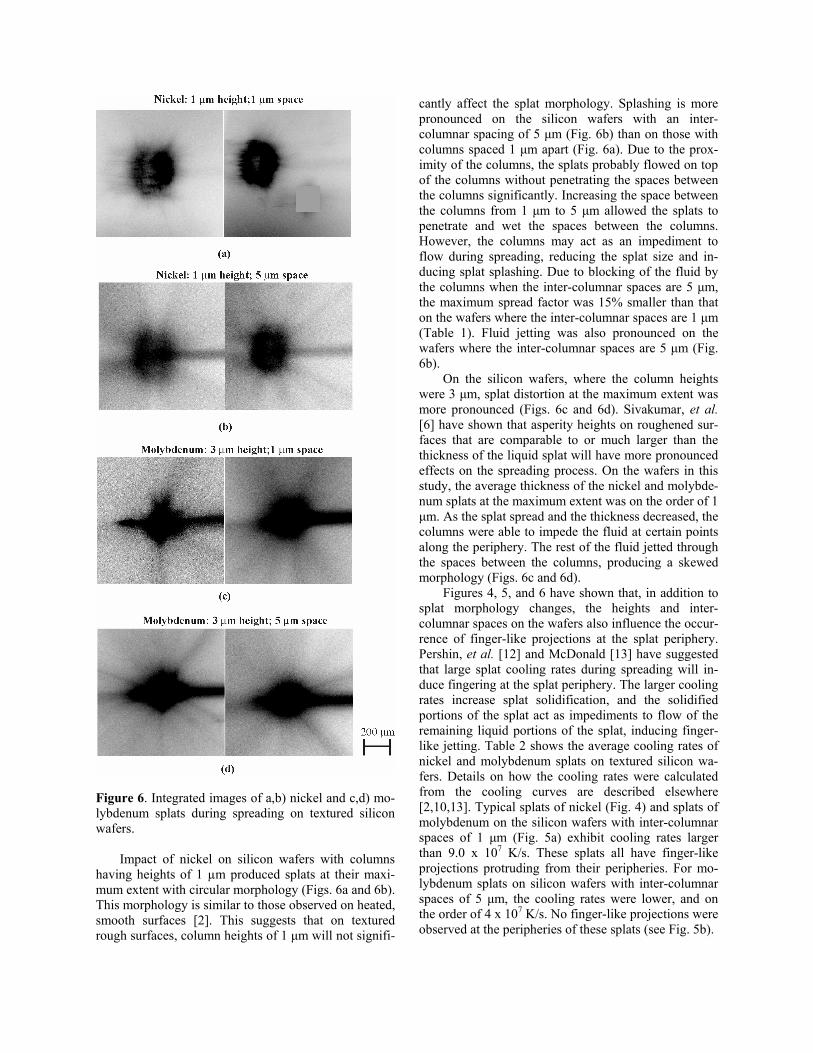
The influence of the column heights on the splat morphology was more clearly observed in images cap-tured in-situ during spreading. Figure 6 shows time-integrated images of nickel (Figs. 6a and 6b) and mo-lybdenum splats (Figs. 6c and 6d) on textured silicon wafers. The maximum splat diameter (Dmax) was taken as the maximum splat extent on the integrated images. The comet-like streak in the images represents the path of the in-flight particle. Table 1 shows the average maximum spread factors of the splats. The maximum spread factor (ȟmax) is defined as the ratio of the maxi-mum splat diameter and the in-flight particle diameter (Do).
Figure 4. Images of nickel splats after solidification on heated textured silicon wafers with 1 ȝm high columns and inter-columnar space of a) 1 ȝm and b) 5 ȝm.
Figure 5. Images of molybdenum splats after solidifica-tion on heated textured silicon wafers with 3 ȝm high columns and inter-columnar space of a) 1 ȝm and b) 5 ȝm.
Figure 6. Integrated images of a,b) nickel and c,d) mo-lybdenum splats during spreading on textured silicon wafers.
Impact of nickel on silicon wafers with columns
having heights of 1 µm produced splats at their maxi-mum extent with circular morphology (Figs. 6a and 6b). This morphology is similar to those observed on heated, smooth surfaces [2]. This suggests that on textured rough surfaces, column heights of 1 ȝm will not signifi-
cantly affect the splat morphology. Splashing is more pronounced on the silicon wafers with an inter-columnar spacing of 5 ȝm (Fig. 6b) than on those with columns spaced 1 ȝm apart (Fig. 6a). Due to the prox-imity of the columns, the splats probably flowed on top of the columns without penetrating the spaces between the columns significantly. Increasing the space between the columns from 1 ȝm to 5 ȝm allowed the splats to penetrate and wet the spaces between the columns. However, the columns may act as an impediment to flow during spreading, reducing the splat size and in-ducing splat splashing. Due to blocking of the fluid by the columns when the inter-columnar spaces are 5 ȝm, the maximum spread factor was 15% smaller than that on the wafers where the inter-columnar spaces are 1 ȝm (Table 1). Fluid jetting was also pronounced on the wafers where the inter-columnar spaces are 5 ȝm (Fig. 6b).
On the silicon wafers, where the column heights were 3 ȝm, splat distortion at the maximum extent was more pronounced (Figs. 6c and 6d). Sivakumar, et al. [6] have shown that asperity heights on roughened sur-faces that are comparable to or much larger than the thickness of the liquid splat will have more pronounced effects on the spreading process. On the wafers in this study, the average thickness of the nickel and molybde-num splats at the maximum extent was on the order of 1 ȝm. As the splat spread and the thickness decreased, the columns were able to impede the fluid at certain points along the periphery. The rest of the fluid jetted through the spaces between the columns, producing a skewed morphology (Figs. 6c and 6d).
Figures 4, 5, and 6 have shown that, in addition to splat morphology changes, the heights and inter-columnar spaces on the wafers also influence the occur-rence of finger-like projections at the splat periphery. Pershin, et al. [12] and McDonald [13] have suggested that large splat cooling rates during spreading will in-duce fingering at the splat periphery. The larger cooling rates increase splat solidification, and the solidified portions of the splat act as impediments to flow of the remaining liquid portions of the splat, inducing finger-like jetting. Table 2 shows the average cooling rates of nickel and molybdenum splats on textured silicon wa-fers. Details on how the cooling rates were calculated from the cooling curves are described elsewhere [2,10,13]. Typical splats of nickel (Fig. 4) and splats of molybdenum on the silicon wafers with inter-columnar spaces of 1 ȝm (Fig. 5a) exhibit cooling rates larger than 9.0 x 10⁷ K/s. These splats all have finger-like projections protruding from their peripheries. For mo-lybdenum splats on silicon wafers with inter-columnar spaces of 5 ȝm, the cooling rates were lower, and on the order of 4 x 10⁷ K/s. No finger-like projections were observed at the peripheries of these splats (see Fig. 5b).
Increased cooling rates imply that physical contact between the splat and substrate is improved and that the splat-substrate contact area is larger [2]. To test this hypothesis, a simple model was developed to estimate the total splat-substrate contact area on the textured silicon wafers. The total contact area was based on the final splat diameter remaining on the wafers after spreading and solidification (see Figs. 4 and 5).
The total surface area per repeating unit of columns on the textured wafer (Atotal) is the sum of the total sur-face area of a column (Acolumn) and the total surface area of the inter-columnar space (Aspace):
Atotal = Acolumn + Aspace. (1)
The total surface area of a column is
Acolumn = w2 + 4(l x w). (2) The total surface area in the inter-columnar space of a repeating unit on the textured surface is
Aspace = 2(b x w) + b2. (3) Figure 2 defines the parameters shown in (1), (2), and (3) above. Substituting (2) and (3) into (1) gives the total surface area per repeating unit as
Atotal = w2 + 4(l x w) + 2(b x w) + b2. (4) The total number of repeating units covered by the solidified splat area is
� �22f
4 bw
Du
�
S, (5)
where u is number of repeating units beneath the splat and Df is the final diameter of the splat reported in Figs. 4 and 5. The total splat-substrate contact area (Acontact) on the textured silicon wafer is Acontact = Atotal x u
= [w2 + 4(l x w) + 2(b x w) + b2] x � �2
2f
4 bw
D
�
S. (6)
Figure 7 shows images of plasma-sprayed nickel after focussed ion beam (FIB) milling. Figure 7a shows that on textured silicon wafers where the column heights were 1 ȝm and the inter-columnar space was 1 ȝm, splat liquid penetration into the inter-columnar spaces was significantly restricted. As a result, it was assumed that on this surface, the column height, l, was zero. Total splat penetration is observed in Figure 7b.
Figure 7. SEM images of nickel splats on textured sili-con wafers with 1 ȝm high columns and inter-columnar space of a) 1 ȝm and b) 5 ȝm after focussed ion beam (FIB) milling.
Figure 8. SEM images of molybdenum splats on tex-tured silicon wafers with 3 ȝm high columns and inter-columnar space of a) 1 ȝm and b) 5 ȝm after focussed ion beam (FIB) milling.
Table 3 shows estimates of the total splat-substrate contact areas. For nickel, the contact area is larger on the textured silicon wafers where the inter-columnar space is 5 ȝm than on those where the inter-columnar space is 1 ȝm. Due to the larger splat-substrate contact area, the cooling rate was 50% larger (see Table 2) and the splats appear thinner (see Fig. 4). For molybdenum, the contact area is larger on the textured silicon wafers where the inter-columnar space is 1 ȝm than on those where the inter-columnar space is 5 ȝm. The large column heights (3 ȝm) probably acted as an impediment to fluid flow in both cases, restricting the size (Table 1) and total splat-substrate contact areas (Table 3). However, the larger number of columns in contact with the splat on the silicon wafers where the inter-columnar space is 1 ȝm, doubled the splat cooling rate (see Table 2). On this surface, the columns acted as fins that penetrated the splat and promoted the conduc-tion of heat, increasing the splat cooling rate. Figure 8 shows SEM images of molybdenum splats after FIB milling to expose the cross-section of the splat. On the silicon wafer where the inter-columnar space is 1 ȝm, there were approximately 20 columns in contact with the splat; on the wafer where the inter-columnar space is 5 ȝm, there were approximately 10 columns in con-tact with the splat across the diameter. Melting of the columns is also clearly visible.
Conclusion
The spreading and fragmentation of plasma-sprayed nickel and molybdenum on silicon wafers that were patterned with micron-sized columns to make a textured rough surface were studied. On wafers with column heights on the order of the splat thickness, the splats exhibited circular morphology; on wafers where the column heights were larger than the splat thickness, a skewed splat morphology was observed, since larger column heights impeded flow during spreading. The cooling rate, as calculated from thermal emission sig-nals, was used as a qualitative indicator of physical contact between the splat and the textured surfaces. On silicon wafers where the column heights were approxi-mately equal to the splat thickness, increasing the inter-columnar space increased the cooling rate. On the sili-con wafers where the column heights were larger than the splat thickness, smaller inter-columnar spaces pro-moted splat cooling since many large columns acted as fins, protruding into the splat. SEM images captured after focussed ion beam milling showed that twice as many columns penetrated the splat when the inter-columnar space was smaller.
A simple calculation was conducted to estimate the total splat-substrate contact area on the textured wafers. It was found that on wafers with small column heights, increasing the inter-columnar spaces, increased the total splat-substrate contact area. This was confirmed by the
increased splat cooling rate on wafers with larger inter-columnar spaces. However, calculations showed that as the column heights increased, the total splat-substrate contact area increased as the inter-columnar space was decreased. This agreed well with the larger splat cool-ing rates observed on patterned surfaces with smaller inter-columnar spaces. References 1. Mehdizadeh, N., Lamontagne, M., Moreau, C.,
Chandra, S., and Mostaghimi, J., J. Thermal Spray
Technol., 14:354 – 361 (2005). 2. McDonald, A., Lamontagne M., Moreau, C., and
12. Pershin, L., McDonald, A., and Chandra, S., “Ef-fect of substrate oxidation on the spreading of plasma-sprayed nickel”, in: 3rd
International Con-
ference on Spray Deposition and Melt Atomization, September 3 – 6, 2006 (Bremen, Germany), Uni-versität Bremen, (2006), 11 pages on compact disk.
13. McDonald, A., Visualization and Analysis of the Impact of Plasma-Sprayed Particles, Ph.D. Thesis, University of Toronto, Toronto, Ontario, Canada (2007).