0 Implementation-Aware System-Level Simulations for IR-UWB Receivers: Approach and Design Methodology Marco Crepaldi 1 , Ilze Aulika 1 and Danilo Demarchi 2 1 Center for Space Human Robotics @Polito, Istituto Italiano di Tecnologia, Corso Trento, Torino 2 Dipartimento di Elettronica (DELEN), Politecnico di Torino, Corso Castelfidardo, Torino Italy 1. Introduction Impulse-Radio Ultra-Wide Band technology (IR-UWB) allocates very large bandwidth with short duration pulses. Interest for research started in 2002 when Federal Communication Commission (FCC) normed the power spectral densities allowed for unintentional and unlicensed UWB radiators in the pre-existing full communication band 0-10 GHz FCC (2002). An ultra-wide band pulse has some unique features compared to conventional wireless signals. If on the one hand, narrowband signals envelope is close to a time unlimited continuous function, on the other hand, in a possible conception pulses can be perfect duty cycled tones having limited time support. Pulses with very short duration occupy very large bandwidth and this is in contrast to the narrowband approach, that subdivides the available spectrum into small slices for efficiently allocating radiated power. IR-UWB is then very interesting because it poses these kinds of challenges, i.e. the use of pulses and the coexistence with the existing RF systems. The use of short duration pulses implies a physical limitation which normally narrowband RF systems are excluded from. These are multipaths, that is reflections from the objects localized in the operating environment. This has conditioned the use of IR-UWB for very high data rates applications because notwithstanding the very large theoretical channel capacity, a very high data rate communication is now almost infeasible with low complexity electronics tackling multipath diversity. IR-UWB has then been proposed for short/medium range Ultra-Low Power (ULP) communication Wireless Sensor Networks (WSN) Bielefeld et al. (2009); IEE (2007); Lecointre et al. (2010); Stoica et al. (2005); Verhelst & Dehaene (2008); Wang et al. (2011). At the transmitters very low average consumed power is possible with aggressive duty cycling, as well as in receivers even if with lower efficiency. Transmitters radiate dBm-order power signals in just 1-3 ns and receivers typically demodulate and synchronize data by detecting the presence of the UWB pulses with time domain computations. One important key-word for understanding how IR-UWB will possibly impact on new ULP applications is “system-level”. The validation of a receiver or a transmitter architecture being aware of the impact of blocks physical implementation prior to full low-level 4 www.intechopen.com
Transcript
0
Implementation-Aware System-LevelSimulations for IR-UWB Receivers: Approach
and Design Methodology
Marco Crepaldi1, Ilze Aulika1 and Danilo Demarchi2
1Center for Space Human Robotics @Polito,Istituto Italiano di Tecnologia, Corso Trento, Torino
2Dipartimento di Elettronica (DELEN),Politecnico di Torino, Corso Castelfidardo, Torino
Italy
1. Introduction
Impulse-Radio Ultra-Wide Band technology (IR-UWB) allocates very large bandwidth withshort duration pulses. Interest for research started in 2002 when Federal CommunicationCommission (FCC) normed the power spectral densities allowed for unintentional andunlicensed UWB radiators in the pre-existing full communication band 0-10 GHz FCC (2002).An ultra-wide band pulse has some unique features compared to conventional wirelesssignals. If on the one hand, narrowband signals envelope is close to a time unlimitedcontinuous function, on the other hand, in a possible conception pulses can be perfect dutycycled tones having limited time support. Pulses with very short duration occupy very largebandwidth and this is in contrast to the narrowband approach, that subdivides the availablespectrum into small slices for efficiently allocating radiated power. IR-UWB is then veryinteresting because it poses these kinds of challenges, i.e. the use of pulses and the coexistencewith the existing RF systems.The use of short duration pulses implies a physical limitation which normally narrowband RFsystems are excluded from. These are multipaths, that is reflections from the objects localizedin the operating environment. This has conditioned the use of IR-UWB for very high data ratesapplications because notwithstanding the very large theoretical channel capacity, a very highdata rate communication is now almost infeasible with low complexity electronics tacklingmultipath diversity. IR-UWB has then been proposed for short/medium range Ultra-LowPower (ULP) communication Wireless Sensor Networks (WSN) Bielefeld et al. (2009); IEE(2007); Lecointre et al. (2010); Stoica et al. (2005); Verhelst & Dehaene (2008); Wang et al.(2011). At the transmitters very low average consumed power is possible with aggressive dutycycling, as well as in receivers even if with lower efficiency. Transmitters radiate dBm-orderpower signals in just 1-3 ns and receivers typically demodulate and synchronize data bydetecting the presence of the UWB pulses with time domain computations.One important key-word for understanding how IR-UWB will possibly impact on new ULPapplications is “system-level”. The validation of a receiver or a transmitter architecturebeing aware of the impact of blocks physical implementation prior to full low-level
4
www.intechopen.com
2
design can possibly lead to significant performance increase and help lower complexity.Based on these considerations, this book chapter shows a methodology used for IR-UWBreceivers simulation, design and conceptualization. A multi-level approach is presented andcontextualized with an implementation example, that is an energy detection receiver. Thisdesign methodology has been already presented in Crepaldi et al. (2007) and extensively usedin Casu et al. (2008). In this book chapter we expand it and provide more comments andconsiderations based on successive works dealing with IR-UWB system-level design.Section 2 considers an Energy Detection receiver as a case study and section 3 introducesthe design methodology after emphasizing its requirements. Later, section 4 applies themethodology to a specific block of the receiver and section 5 shows the obtained simulationresults. Section 6 concludes the chapter.
2. A case study: the Energy Detection receiver
IR-UWB Energy Detection receivers represented mostly the number one choice for WSN andhave been widely integrated and researched starting the second half of 2000-2010 decadeCrepaldi et al. (2010); Daly et al. (2009); Lee & Chandrakasan (2007). Energy detectionreceivers are robust and of easy implementation notwithstanding being non-coherent,therefore sub-optimal. In the beginning, research was focused on conceptualized architecturesthat studied the communication performance of IR-UWB and attempted to solve somesystem-level issues. An example for non-coherent M-PPM receivers is given in Carbonelli& Mengali (2006). The proposed architectures did not deeply account for circuit-levelimplementation details. Starting from this first conceptualization mechanism, first energydetection receivers have been proposed Stoica et al. (2005), Lee & Chandrakasan (2007).By then all the required system-level performance figures were validated on silicon forthe first time. This, and the successive receivers proposed by then, aimed towards lowerenergy consumption or to increase performance of some of these reference points. In thisbook chapter we refer to a somewhat old energy detection receiver scheme, in which anAnalog-to-Digital Converter (ADC) is used for data demodulation as well the use of otherblocks that differ compared to recent implementations. Here, we explicitly utilize this schemebecause it represents a case study, and still, valid ideas can emerge from the analysis of thissystem from cross-sectional views.A standard energy detection receiver block scheme is depicted in fig. 1. The completetransceiver is assumed to be fully implemented as a silicon System-on-Chip (SoC) andat this stage the transmitter is assumed to be only behaviorally modeled. The antennaswitch commutates the wideband antenna to receiver and transmitter ends, while an externalBand-Pass Filter (BPF) ensures that on-chip generated UWB pulses satisfy the FCC mask and,at the same time, filters out-of-band interference from the received ones. The energy detector,depicted in the front-end part is composed of a linear amplification block, the Low-NoiseAmplifier (LNA), Variable Gain Amplifiers (VGA) a squaring unit and an Integrate&Dump(I&D). The receiver computes the raw pulse energy. By assuming that integration genericallystarts at ta and ends at tb, Ar(t) is signal at the output of the VGA, where A is the gain of theprevious blocks, the energy E at the output of the I&D is,
E =∫ tb
ta
A2r(t)2dt (1)
To run both synchronization and demodulation the receiver circuitry operates on ta andtb to detect for example the maximum energy peak and, for 2-PPM receivers, activate
80 Novel Applications of the UWB Technologies
www.intechopen.com
Implementation-Aware System-Level Simulations for IR-UWB Receivers: Approach and Design Methodology 3
Transmitter
LNA
DC/PMU
VGA
RF
Analog
Data
Demod &
Processing
AGC
Receiver front end
Simulated Blocks
Antenna Switch
Digital dataAnalog data
Antenna
UWBTRX
( )2
Counter
I & D ADC
BPF
Synch
Mixed
Digital
NE/PS
Fig. 1. Energy Detection transceiver block scheme Crepaldi et al. (2007).
integration once pulses timing is acquired at the correct ’1’ or ’0’ bins. For gain control thereceiver operates on parameter A with an digital-to-analog feedback from the demodulationchain. After energy is calculated it is quantized with an ADC and then processed by theback-end that can implement a threshold based demodulation algorithm for OOK, or a relativecomparison as in the case of 2-PPM. Here the receiver operates with 2-PPM modulation.The Data processing block controls also the synchronization unit, that operates similarlyto a Delay-Locked-Loop (DLL) for searching the maximum energy peak within a knownpreamble. The Automatic Gain Control unit (AGC) automatically sets the front-end gainbased on the digitized energy. The NE/PS block, namely Noise Estimation&Preamble Sensingblock, helps detecting the presence of a preamble once the receiver is activated and collectsenergy samples from channel when no pulse is transmitted. This helps assessing the clearanceof channel as soon as receiver is activated, therefore allowing system shutdown in case nopacket is received. Data saved by this digital block is used for adjusting the gain of thereceiver front-end for allowing the input range adaptation of the input signal for I&D andconsequent A/D conversion. Note that here, receiver sensitivity is defined by the LNA, thatshall have the highest gain and the lowest noise figure. The noise figure of the successiveVGA units is not as influent as for the first stage because input-referred noise figure iscalculated by propagating each amplifier noise figure with Friis formula. Notwithstandingthis, the receiver must provide enough amplification to process the UWB pulses, overcomethe non-linear law of the squaring unit and the channel path-loss that highly depends on theobjects distributed in space. The Counter in the high-level architecture is useful UWB pulsesTime-of-Flight calculation, in this case with a Two-Way-Ranging (TWR) packet exchange(defined in section 5). The Duty Cycling/Power Management Unit (DC/PMU) implementsreceiver duty cycling and deactivates the front-end units to save energy when the receiveris idle. The full implementation of this block requires the definition of the complete packetexchange mechanism as well as detailed information on each single block of the receiver.
81Implementation-Aware System-LevelSimulations for IR-UWB Receivers: Approach and Design Methodology
www.intechopen.com
4
Therefore, the complete development of the DC/PMU must be faced at the end of the designbut it shall not be considered less important than the others.It is worth mentioning that our methodological approach is devoted to system-levelimplications rather than being focused on circuit-level challenges. As recent research shows,we believe that one of the next steps for PHY IR-UWB systems research has to regard bothdecreasing energy consumption and solving problems from a more general and wide-sensesystem-level view Gorlatova et al. (2010).
3. The substitute-and-play design methodology
3.1 Simulator and target system
The methodology outlined here is applied on a specific simulation tool called ADVanceMS(ADMS, Mentor Graphics, now Questa ADMS) that allows multi-language descriptionswith multi-resolution simulations. It supports VHDL-AMS, Verilog-AMS, VHDL, Verilog,SystemVerilog, SPICE1 and SystemC in the same simulation environment. The Very HighSpeed integrated circuit Hardware Description Language (VHDL), similarly to Verilog, iswidely used to logically and behaviorally describe digital circuits, modular by constructionand based on a very simple math. VHDL is a concurrent language in which every describedprocess works in parallel with the others. Communication among processes is based onevents. Before evolving to the next time step, the simulator engine processes a single listin which all process events are queued. While this task is accomplished simulation timeis frozen. The VHDL-AMS (AMS is for Analog and Mixed-Signal extensions) languageis an extension of the common VHDL IEEE (2007) and adds directives and constructs tosupport at the same time both digital concurrent and simultaneous statements. These lastones, are used to allow the implementation of the continuous-time nature of analog systems.Continuous-time simulations are not based on events, but on the computation of quantitiesrepresenting the solution of a continuous mathematical model. In a mixed-signal simulationthe inter-communication between these two totally different worlds is ensured by the softwaretool that handles the different VHDL constructs depending on the cases and interfaces themto a simulation kernel, for example SystemC.With the same continuous-time granularity the tool can include SPICE-level netlists in thedescription. Netlists can be directly interfaced to VHDL-AMS, therefore a block can painlesslyjump from a behavioral world to the voltage and current domain of silicon devices. Also, othercommercial tools such as Cadence IC provide multi-level and multi-resolution descriptionsbut still they are based on an analog point of view, referring to the system-level use ofcircuit blocks instead of exploiting the flexibility of a digital description language formalism.Another example is Advanced Design System (ADS, Agilent) that enriches its system-leveldesign flow with low-level electro magnetic simulations. All these tools are frameworksmeant to bridge multiple description languages and simulation tools transparently to theuser. Here, with this methodology, we believe that that the use of a single and homogenousformalism, with possibly a single simulator, can make the difference.The evaluation of system-level performance of an IR-UWB system in time-domain isimportant. As an example, let us consider Duty Cycling (DC). Ideally an IR-UWB receiverhas to be kept operating for time durations on the order of few nanoseconds sufficient forreceiving pulses from channel and be shut-down for the remaining time to save power
1 In the following paragraphs we will refer to SPICE descriptions by referring to the name of the MentorGraphics simulator, ELDO.
82 Novel Applications of the UWB Technologies
www.intechopen.com
Implementation-Aware System-Level Simulations for IR-UWB Receivers: Approach and Design Methodology 5
consumption. Typically RF front-ends have resonant loads therefore, depending on theimplementation, spurious pulses can be erroneously generated whenever a hard digitalactivation signal operating on active amplification elements is toggled. If the RF amplifiers aresimulated only in AC and integrated without a time-domain verification, at the measurementstime the system performance can be seriously compromised or even the receiver cannotoperate because the successive baseband and backend units are saturated. Therefore, in thismethodology we stressed out the time-domain aspect of simulations and to save runtimeused the multi-resolution feature to activate only the most important non-ideality requiredfor obtaining figures as much close as possible to the physical verification. Unfortunatelyrunning time-domain simulations requires the full large signal expressions of transistors, ifsimulation includes circuit level blocks, or to solve differential equations whether a high-levelbehavioral model is conceived. The multi-resolution aspect is then fundamental for obtainingresults in a reasonable time because system-level figures of IR-UWB receivers are based oniterative statistical analyses.Implementation-aware actions on IR-UWB transceivers design require the identification ofperformance figures that depend on system-level constraints. The most common figuresare typically related to Bit-Error-Rate (BER), for communication purposes and, in thecase of IR-UWB for ranging applications, to the estimation of the Time-of-Flight (ToF).The UWB channel is statistical, therefore determining these system-level data impliesrandomizing different multipath realizations according to a specific operating environment,i.e. indoor office, residential, industrial, outdoor, open outdoor, and for Line-Of-Sight (LOS)or Non Line-Of-Sight (NLOS) links IEE (2004). Also, the computation of ToF with TWRschemes requires the modeling of a complete packet transmission mechanism without idealsynchronization. In communications, for bit error-rate tests large random data needs to betested. Take for example a 10−6 BER: theoretically to obtain this single error-rate point atleast 100 points are required for high confidence and this implies randomizing an averageof 108 pulses. Note that from a pure communication point of view all these functionalitiescan be easily implemented with any high-level modeling language e.g. Matlab but this lacksof flexibility because top-down refinement of heterogeneous blocks is typically not possible.The use of a multi-description modeling tool permits an easy “context switching” between ahigh-level model to a circuit-level or SPICE post-layout netlists without having to interfacethe description. This flexibility is not relative only to the simulation tool itself but to thedescription language and in particular to the use of an homogeneous interface betweendescriptions. Let us consider an Integrate & Dump unit. Basically, the block shall have aninput, an output and an integrate/dump control. Alternatively, if description is at a very highabstraction level control signal can be potentially undefined. These terminals not necessarilyconvey voltage or current but instead can be, if present, symbolic that only in a successivestep are mapped onto a physical counterpart. The use of a priori homogeneous interfacingbetween different descriptions avoids burdensome conversion times and can be useful fordefining electrical interconnections from early design stages.System-level simulations aiming towards physical implementation predictions, must beenriched with many circuit-level non-ideality concerning silicon integration. Electro-StaticDischarge (ESD) protection circuits, bondwire for die soldering on packages and inductiveor capacitive parasitic couplings are few of the possible non-ideal effects. These, however,concern circuit-level design and at first design concept phases these can be disregarded,therefore assuming that chip-level integration countermeasures can efficiently tackle them ina next step. For example, if a cascoded tuned amplifier LNA requires a very well controlled
83Implementation-Aware System-LevelSimulations for IR-UWB Receivers: Approach and Design Methodology
www.intechopen.com
6
to-ground parasitic inductance then this aspect has to be tackled at die-level floorplanningwhen the number of PAD is decided, therefore at circuit-level design steps. Instead, if theboundary conditions among two or more functional units represents a critical point, thisshall be included in system level models. Also, the same parasitic can play different rolesif shared among other circuit blocks. For example, if parasitic inductance influences much theoperation of a block, for example an UWB coherent correlator, then this shall be included inthe system-level model. From this analysis we conclude that the definition of the parametersrequired in simulation is fundamental.Non-ideality can depend on many different factors but a flexible high-level simulationrequires that they can be effectively modeled as generic parameters. For example, basedon circuit-level details, the squarer unit in energy detection receivers, if not differential, canoriginate additionally to the ()2 term a linear by-product that depends on input signal levelHan & Sanchez-Sinencio (1998). A high-level parametric behavioral modeling requires theimplementation of a mathematical relationship that covers, in the most general conceptionand with sufficient confidence, the behavior of the circuit-level unit in all the operatingconditions. In a high-level methodology this is particularly important because system levelsimulations are not meant to be a mere verification but instead shall represent a startingpoint for deriving useful design constraints. The inclusion of circuit-level descriptionsat system-level with a uniform and flexbile language serves as inspection and analysis.Successive chip-level integration can be then easily derived by painlessly placing and routingall the blocks at their lowest layout description level.
3.2 Methodological assumptions
Based on the previous analysis, a design methodology for electronics systems shall be referredto at least three important respects: uniformity, partitioning and refinement. Uniformity can beread as the requirement of having an homogeneous formalism to describe the operation ofa system. Partitioning can be read as the effort a designer makes for physically mappingthe conceptual operation of a system according to very well defined rules. Refinement canbe read as the enrichment of physical non-ideality applied to a pure mathematical modelto more precisely describe physical behavior. Take for example digital design. Hardwaredescription language as VHDL or Verilog are uniform, because they are completely portableand allow an homogeneous description of a block. The languages permit both gate-leveland behavioral-level descriptions at the same time. The logic conception of digital circuitsinherently permits a partitioning, that is the identification of input and output signals.Refinement is also possible because, provided that a block has the same inputs and outputs,its description can pass from behavioral to structural, therefore getting closer to single logicgates.With circuit-level design we have very different aspects. The basic building blocks are notlogic gates but devices with a particular electrical interface. In digital domain interfacecomprises purely logical inputs outputs while here the same input and output terminals areenriched with continuous power by voltage and current. Parasitic are very important in RFdesign and the well defined input/output paradigm valid for digital circuits is compromised.In the above reading key, couplings between two near blocks on the same silicon chip cangenerate other inputs and outputs, even if their physical counterpart is a fF order capacitance,a pH order coupling inductance or a GΩ resistor. An RF amplifier having a single input oroutput, after layout can have more physical interconnections with other blocks that share thesame die. In this digital-like input/output key, the effect of parasitic can be also modeled
84 Novel Applications of the UWB Technologies
www.intechopen.com
Implementation-Aware System-Level Simulations for IR-UWB Receivers: Approach and Design Methodology 7
impacting on a given electrical signal, i.e. bandwidth or gain decrease without having tomap it as an additional input or output. While the modeling of parasitic effects can be moresystematic in digital design (consider for example delay of logic gates), in the analog worldthis is more complex because it depends on physical design. Filling the modeling gap betweenanalog and digital worlds with a uniform methodology can be possibly obtained by using adescription language that forces the same partitioning as in digital domain and at the sametime has enough flexibility for being used in the digital simulation domain. Description isnot the only aspect that shall be considered. Attention regards also the simulator itself andtherefore its inherent capability of accepting hardware described with different languages.Therefore, the design methodology presented here refers to a simulator with which multipledescription languages with a uniform formalism are contemplated. Fig. 2 schematizes theinteractions between simulation and hardware worlds.
Q
D Q
CLK
L1
L3
L3
L3 L3
L3
L3
L2
Simulation Hardware
performanceSystem level
Multi languageMulti resolution
L2
L3
L1
D( . ) = DescriptionLA( . ) = Language
LX= Level X
Environment
SemanticsFormalism
f(D(L1), D(L2), D(L3))
Simulator Language
LA(L1)
LA(L3)
FlexibilityCoexistence
Circuit level
High level
Fig. 2. Simulator and language in a multi-level description.
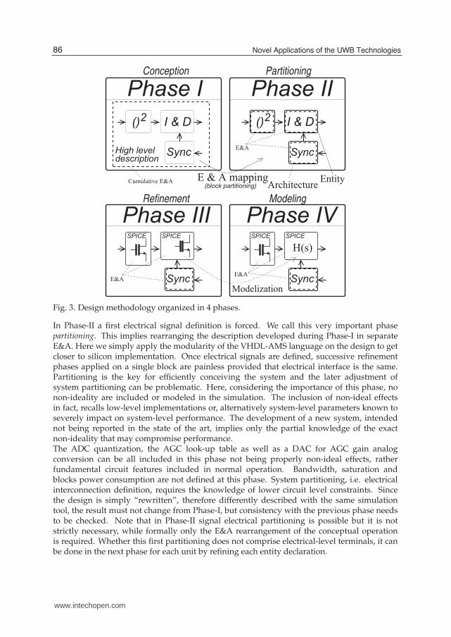
3.3 Design methodology
The design methodology outlined in this work is organized in four phases. During Phase-Ithe receiver, or generally the IR-UWB system is behaviorally defined and a first high-levelmodel is generated. This phase is known as conception. In the case of our Energy Detectionreceiver front-end this implies behaviorally modeling e.g. LNA, squaring unit, Integrate andDump and the Analog-to-Digital Converter (ADC). Note that in the example of figure 3 thefront-end is shown but the methodology can be applied to complete systems, even includinga dedicated backend for bit and symbol synchronization and demodulation, because VHDLand VHDL-AMS lie on the same domain. At this abstraction level, the description stillrecalls the formalism of a high-level modeling language e.g. Matlab since an electricalinterface is not defined yet and the complete system is packed onto few VHDL-AMS processdisregarding the complexity its implementation may imply. Figure 3 (Phase I) shows asingle Entity-Architecture (E&A) couple comprising a complete energy detection receiverfront-end. At this point, the model is validated by checking consistency with high-levelmodels developed in Matlab or in other high-level languages applied on the system-levelfigures previously mentioned. Here, from the engineering point of view, the main effortconsists of defining the system operation without forcing a design partition that is mandatorytowards physical-level implementations.
85Implementation-Aware System-LevelSimulations for IR-UWB Receivers: Approach and Design Methodology
www.intechopen.com
8
()2()2
Phase II
E & A mapping(block partitioning)
Cumulative E&A Entity
Partitioning
Refinement Modeling
Conception
Architecture
E&A
E&AE&A
Phase I
descriptionHigh level
I & D
Sync Sync
I & D
SPICE SPICE
Phase IVPhase IIISPICE SPICE
H(s)
ModelizationSync Sync
Fig. 3. Design methodology organized in 4 phases.
In Phase-II a first electrical signal definition is forced. We call this very important phasepartitioning. This implies rearranging the description developed during Phase-I in separateE&A. Here we simply apply the modularity of the VHDL-AMS language on the design to getcloser to silicon implementation. Once electrical signals are defined, successive refinementphases applied on a single block are painless provided that electrical interface is the same.Partitioning is the key for efficiently conceiving the system and the later adjustment ofsystem partitioning can be problematic. Here, considering the importance of this phase, nonon-ideality are included or modeled in the simulation. The inclusion of non-ideal effectsin fact, recalls low-level implementations or, alternatively system-level parameters known toseverely impact on system-level performance. The development of a new system, intendednot being reported in the state of the art, implies only the partial knowledge of the exactnon-ideality that may compromise performance.The ADC quantization, the AGC look-up table as well as a DAC for AGC gain analogconversion can be all included in this phase not being properly non-ideal effects, ratherfundamental circuit features included in normal operation. Bandwidth, saturation andblocks power consumption are not defined at this phase. System partitioning, i.e. electricalinterconnection definition, requires the knowledge of lower circuit level constraints. Sincethe design is simply “rewritten”, therefore differently described with the same simulationtool, the result must not change from Phase-I, but consistency with the previous phase needsto be checked. Note that in Phase-II signal electrical partitioning is possible but it is notstrictly necessary, while formally only the E&A rearrangement of the conceptual operationis required. Whether this first partitioning does not comprise electrical-level terminals, it canbe done in the next phase for each unit by refining each entity declaration.
86 Novel Applications of the UWB Technologies
www.intechopen.com
Implementation-Aware System-Level Simulations for IR-UWB Receivers: Approach and Design Methodology 9
Once system partitioning is complete, the electrical interface of all the blocks in the IR-UWBsystem are defined. We are now ready to increase the details in each block. For this reason,Phase-III is called also refinement. With refinement, signals partitioned in Phase-II assumea circuit-level meaning. Every important circuit-level non-ideality is modeled according tocontinuous time or digital statements and included in the architecture. The importanceof this phase regards the identification of the non-ideal effects that impact on system-levelperformance, or, if the system leads the state-of-the-art, even on its basic operation. Effortsin the definition of the number of non-ideality of their description is an important trade-offbecause very accurate models can severely impact on simulation runtime or excessive effortson this side can waste time and compromise the overall system-level performance inspection.For energy detection receivers for example, modeling of compression in the front-end isimportant e.g. for understanding the impact on interference rejection, but still, since thesystem computes the raw energy of the UWB pulses with a squarer, this is not extremelyimportant. Dedicating weeks of research time on this would avoid taking important decisionsnext or would block the project at its beginning, while other problems may rise duringcircuit-level design or chip-level integration.Phase-III is not only related to the inclusion of non-ideality to the previously idealizedblocks. Provided that an homogenous electrical interface derived from Phase-II in theentity declaration of every VHDL-AMS unit is given the complete VHDL architecture can beswitched. This enables the replacement of the full VHDL-AMS modeling with transistor-levelSPICE models extracted from Cadence Front-end to Back-end or IC Station (Mentor Graphics)other front-end circuit design tools. The description can be also extracted from layout.This Substitute-and-Play (S&P) philosophy allows the identification of the impact of blocksrefinement on system-level performance figures. This is very important because it permitsarchitectural analyses by intelligently exploring all the possibilities without focusing on asingle abstraction level. Here, a heterogeneous multi-level description can help understandingfaster the problems that may arise when solid-state circuits are tested. Provided thatrefinement is intelligently run, performance e.g. on ranging, demodulation, synchronization,transceiver packet exchange, power consumption, can be forecasted and decision takenwhether constraints are not met.IR-UWB demands time-domain simulations and a complete refined system, even if not forall its blocks, can require very high runtimes especially when statistical tests are executed.Notwithstanding the computational power of workstation and servers keeps increasing aswell as code parallelism in software, due to the short duration pulses high simulation accuracyis required and a complete 10 or 100 s packet exchange simulation can require days or evenmore. This applies also e.g. for PLL, where full SPICE level time-domain simulations areimpractical (and in this context also inaccurate) Lai et al. (2005). Moreover, it can result that theeffect of some circuit-level blocks severally impacts on system-level performance but cannotbe neglected in the description. Therefore, we define a successive Phase-IV, called modeling orback-annotation, that aims at the inclusion of the relevant circuit-level non-ideality extractedfrom the transistor-level description of Phase-III. This can be accomplished in two differentways. The already modeled parameters are refined based on pure circuit level simulation, or,if the non-ideality discovered during Phase-III was not included previously the architecture isredesigned by keeping the same entity definition. The refined models can be used in Phase-IIIfor running again simulations and obtaining further results.The full design methodology is applied on the I&D unit of our Energy Detection receivercase study as an example. Next paragraph will focus on the design of the block and all
87Implementation-Aware System-LevelSimulations for IR-UWB Receivers: Approach and Design Methodology
www.intechopen.com
10
the hypothesis used for its conceptualization will be explained and identified in the outlinedmethodological key.
4. S&P contextualization: The I&D block design
Fig. 4 shows also the partitioned entity of the I&D and the entity declaration structure. At thehighest abstraction level, the I&D electrical boundary is not defined and simply implementsthe math function
∫x(t)dt, where x(t) is input signal. x(t) has not a physical counterpart
nor it is single-ended or differential and integration output is a quantity that is neithervoltage nor a current. A control signal is implicitly defined among the other high-levelstatements that control the computation of the formula. This integrator has been included inthe high-level model and a first consistency check with a Matlab model has been completed.When description enters Phase-II, some circuit level properties must be considered. These aremainly related to 1) power supply, 2) control signals, 3) input and output electrical features(single-ended or differential, AC or DC coupled, current or voltage). By satisfying theseconstraints, valid for this specific case, the electrical interconnection boundary can be defined.The I&D is a pure analog unit, that has to cope with relatively high frequency signals2.Therefore, this block is not critical from the RF point of view and a single power supplyand ground connection pin can be considered. Notwithstanding this, the block is critical atsystem-level. In the case of the LNA for example, having multiple power supplies can helpreducing inductance parasitic and, depending on circuit-level design, it can be fundamentalfor matching. Therefore, modeling multiple power supply pins can be useful even at thisabstraction level, and the problems that may arise can be directly tackled here rather thansuccessively, when the floor plan is defined and circuit blocks placed down. A very firstconstraint we had in the design on the energy detection receiver was that it had to be fullydifferential, therefore fully differential input and outputs were assumed, in fig. 4 the couplesInp-Inm and Out_intp-Out_intm, in particular DC coupled voltage signals. For integrationcontrol signals the discussion is more complex because the use of a single ended or adifferential signal (one, vs. two terminals) depends on the internal implementation of the unit.Homogeneously, we assume also perfectly differential voltage signals Controlp-Controlm.In this very first implementation we assume that integrator is the gm-C structure depicted infig. 4. The transconductor transforms the input voltage into differential current and chargesa load capacitor C. When control signal Controlp-Controlm is active integration is run,while when it toggles to ’0’ integration is reset. The biasing circuit is connected to Vbias1,Vbias2 and to Vbias3, it consists of two self-biasing stages that generate the required voltagesfor both transconductor and Common Mode Feedback Network (CMFB), not shown here forsake of brevity. According to the state-of-the-art simpler integrator structures are possible andthey can be single ended and much simpler than those depicted here Lee & Chandrakasan(2007). At this point, the target was the replacement of a BiCMOS integrator by then used ina first implementation Stoica et al. (2005) with a lower cost CMOS integrator. Note that at thispoint the I&D architecture boundary has been fully defined. From an electrical point of viewthis enables the VHDL architecture switching among different Phase-III domain models. Forexample, a VHDL-AMS behavioral model, with the given electrical interface can be painlesslysubstituted with the equivalent circuit-level or layout-description.
2 Note that after squaring, the useful portion of the spectrum of a UWB signal of bandwidth B is atbaseband, [0, B/2], e.g. for a standard UWB pulse having a 500 MHz bandwidth, this corresponds tooperating in the band 0-250 MHz.
88 Novel Applications of the UWB Technologies
www.intechopen.com
Implementation-Aware System-Level Simulations for IR-UWB Receivers: Approach and Design Methodology 11
Inp
Inm
Inp
Inm
Inp
Inm
Interface nodes
Internal nodes
Phase II
if selection=’1’ use vo’Dot == K*vin; else vo=0.0; end use;
Entity
Architecture
Phase IV
Entity
Phase III − TL
Phase I processbegin
end process;
...
...energy’Dot <= squared*K;
Entity
Architecture
if selection=’1’ useA*vin−B*vo1−C*vo1’Dot==0;D*vo1−E*vo−F*vo’Dot==0;
else vo1 == 0.0; vo = 0.0; end use;
Architecture
Entity
vovin
GndVdd
I & D
Out_intmOut_intp
Controlm
Controlp
GndVdd
Out_intmOut_intp
Controlm
Controlp
GndVdd
selection
vovin
I & D
I & DI & D
I & D
IR UWB RX
Architecture
selection
Out_intp Out_intm
Controlm
Controlp
UWB_in Data_out
LV
LV
LV LV
Vcmfb
CMFB
C
Outp
Outm
Vbias1 Vbias2
Inp
Vin
Controlm
Inm
Vdd
Gnd
Vbias3 Vdd
Out_intm
Out_intp
Voutd
LV
LV LV
LV
LV
Transconductance Amplifier Integration switches
Controlp
Outm
Outp
Vcmfb
Gnd
Fig. 4. I&D circuit at the circuit-level design and partitioning level.
With circuit-level simulation the AC behavior of the I&D can be easily extracted. This isreported here on fig. 5 from Crepaldi et al. (2007). The integrator operates from 1 MHz to1 GHz, has an additional low-pass transfer function, and not ideally infinite DC gain. Thesecond pole at high frequency is due to parasitics of the devices. Note that the useful partof the UWB signal is concentrated from 0 to 250 MHz for a 500 MHz pulse and the behaviorof the integrator at very high frequency is not fundamental. The non-infinite DC gain is aloss therefore limiting the maximum length of the integration window. At this point, this ACmodel can be included in the Phase-III VHDL-AMS models to speed up simulation time. Notethat by including the AC model only non-linearities and saturation of the transconductor arenot accounted for. This is a clear example of the mandatory requirement of Phase-IV, that isan intelligent inclusion of the relevant non-ideality derived from transistor-level design. Inthe case the required system-level simulation explicitly requires accounting for this non-idealeffect, then, the backannotation shall be enriched, or alternatively the full circuit shall beincluded and other blocks non-ideality deactivated to speed-up simulation time. Beforeapplying the substitute-and-play approach, consistency with ideal (Phase-II) and VHDL-AMSmodels has been checked. As shown in fig. 5, the backannotated model and the AC circuitsimulation of Phase-III match.
89Implementation-Aware System-LevelSimulations for IR-UWB Receivers: Approach and Design Methodology
www.intechopen.com
12
Fig. 5. AC response of the I&D circuit and Phase-II and III models Crepaldi et al. (2007). TheIDEAL and VHDL-AMS models overlap.
The connection of transistor level descriptions with ideal blocks can require specificconsiderations, not only related to the modeling language itself but on the electrical featuresresulting from blocks interfacing. Take for example a fully ideal Phase-II model of thesquarer. A possible VHDL-AMS description can include only the simultaneous statementvsquare==K*vin**2.0;, where square and vin are across quantities defined on twocouples of differential terminals. If this is the case, then input and output impedance of thesquarer is completely disregarded. If the squarer modeled according to this simple statementis connected to the I&D the resulting integration voltage would be compromised becausecommon mode voltage is disregarded. Therefore, in such cases the inclusion of a boundaryelement is fundamental for brigding the ideal world to a full custom electrical interface. Theseboundary elements are inherently included in the surroundings units. In this work, properboundary elements, operating on the DC level of vin have been included.Fig.6 shows a transient simulation of the integrators during three different modeling phasesII, III and IV. Notwithstanding a gain mismatch output is still energy, that is the integral of thesquared signal.
5. System-level simulations and results
One very interesting feature of Impulse-Radio UWB regards the possibility of determiningthe pulses time of flight, that is, the distance between two transceivers. Since UWB pulses arevery short, the accuracy with which distance can be estimated can be very high. For example,recent receivers are designed with fine synchronization circuits reaching accuracies of few
90 Novel Applications of the UWB Technologies
www.intechopen.com
Implementation-Aware System-Level Simulations for IR-UWB Receivers: Approach and Design Methodology 13
Fig. 6. Transient response of the I&D circuits obtained from different modeling phasesCrepaldi et al. (2007).
millimeters Chu et al. (2011). Pulse radio was thought also to serve localization purposeseven in space applications Ni et al. (2010). IR-UWB can be easily applied to biomedicaldevices because pulses are reflected differently depending on dielectric properties mismatchesamong different mediums. This enables applications in Breast Cancer Detection and wirelessbiometric parameters sensing. Here, we applied the methodology to Bit-Error-Rate testsfor wireless link quality inspection, and to Two-Way-Ranging related to ToF estimationperformance.Figure 7 shows a graphical representation of the effect of the I&D substitution on ourenergy detection IR-UWB system. The figure shows also a graphical representation of theTWR mechanism implemented between two transceivers3. Two-Way-Ranging is a packetexchange mechanism that is based on the transmission of two packets, a request packet andan acknowledge packet between two transceivers A and B. The Time-of-Flight is calculatedat the transceiver B, after having received the acknowledge packet from transceiver A. TheToF calculation is based on the determination of the exact leading edge of the UWB pulseswith a proper synchronization algorithm. A very common synchronization algorithm, alsocalled window integrator, is based on the determination of the time when the sampling of themaximum UWB energy occurs. It is based on an integration window shift within a fixed pulserepetition period. The shift is realized by a dedicated DLL and phase selector that sequentiallyshift the control signal of the I&D. After a full exploration within the Pulse Repetition Interval(PRI) the clock phase corresponding to maximum energy is selected. The accuracy of thealgorithm depends on the integration window shift, that for coarse synchronization can be
3 Note that other ranging schemes are possible, for example in Ni et al. (2010) Time-Difference-Of-Arrival(TDOA) is used.
91Implementation-Aware System-LevelSimulations for IR-UWB Receivers: Approach and Design Methodology
www.intechopen.com
14
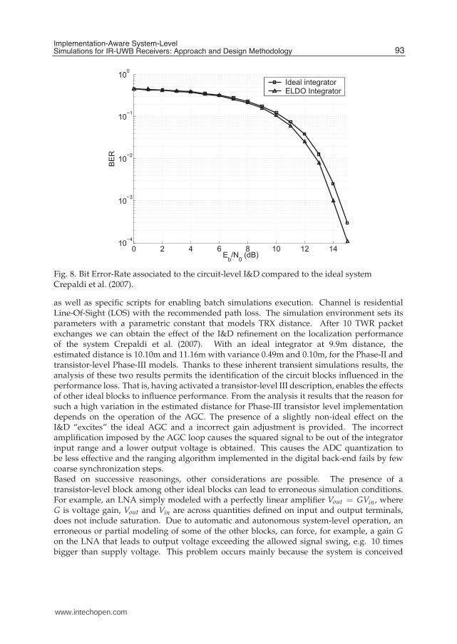
on the order of 5 ns or for fine synchronization even less than 1 ns. Here we applied thiswindowed integrator for both coarse and fine synchronization. Transceiver B system clockphase is different with respect to transceiver A, therefore the acknowledge packet mustinclude information on both the processing time offset of TRX A and the synchronizationphase used for detecting the maximum energy. Transceiver B, processes this information and,according to its synchronization phase, calculates the ToF, therefore distance. Details aboutthe full mechanism can be found in Casu et al. (2008).Bit-Error-Rate is determined in presence of Additive White Gaussian Noise (AWGN). Itsdetermination implies the inclusion of the Salleh-Valenzuela UWB channel model in thesimulation environment with a VHDL-AMS formalism IEE (2004). Natively, the model isimplemented in Matlab and here its VHDL-AMS description is based on text files withrendered saved data samples issued with a constant time step. Fig. 8 shows the effect of
Ideal
Transmitter
LNA VGA
Antenna Switch
( )2
I & D ADC
E /Nb 0
BER
real distance (m)
A
B
1 2
NclkT
OF,1T
OF,2
TT0 1
1 2
SPICE
Transmitter
LNA VGA
Antenna Switch
( )2
ADC
Boundary interfaceIdeal
B
A
estimated distance (m)
I & D
1, 2 = Request, Ack packets
N = Fixed processing timeclk
A, B = Transceiver A and Transceiver B
OF,1
Multi language
Simulator
VHDL AMS/VHDL/SPICE
T , T = time of flight (same CLK)OF,2
Fig. 7. Deactivation of non-ideal effects during system-level simulation andTwo-Way-Ranging.
Phase-III integrator on the BER performance of the system Crepaldi et al. (2007) as a functionof Eb/N0 (proportional to Signal-to-Noise Ratio). The BER curve is slightly shifter becausethe pole2 of the integrator additionally filter input noise out of the squarer. If other blocks areimplemented at transistor-level then, noise filtering increases. The results demonstrate thatthis design methodology permits the determination of transistor-level non-ideality at higherabstraction level.With the Salleh-Valenzuela channel VHDL-AMS model TWR ranging simulations are alsopossible. Detailed TWR simulation results are reported in Casu et al. (2008). Two instancesof the same IR-UWB transceiver schematized in 1 have been included in the environment
92 Novel Applications of the UWB Technologies
www.intechopen.com
Implementation-Aware System-Level Simulations for IR-UWB Receivers: Approach and Design Methodology 15
0 2 4 6 8 10 12 1410
4
103
102
101
100
Eb/N
0 (dB)
BE
R
Ideal integratorELDO Integrator
Fig. 8. Bit Error-Rate associated to the circuit-level I&D compared to the ideal systemCrepaldi et al. (2007).
as well as specific scripts for enabling batch simulations execution. Channel is residentialLine-Of-Sight (LOS) with the recommended path loss. The simulation environment sets itsparameters with a parametric constant that models TRX distance. After 10 TWR packetexchanges we can obtain the effect of the I&D refinement on the localization performanceof the system Crepaldi et al. (2007). With an ideal integrator at 9.9m distance, theestimated distance is 10.10m and 11.16m with variance 0.49m and 0.10m, for the Phase-II andtransistor-level Phase-III models. Thanks to these inherent transient simulations results, theanalysis of these two results permits the identification of the circuit blocks influenced in theperformance loss. That is, having activated a transistor-level III description, enables the effectsof other ideal blocks to influence performance. From the analysis it results that the reason forsuch a high variation in the estimated distance for Phase-III transistor level implementationdepends on the operation of the AGC. The presence of a slightly non-ideal effect on theI&D “excites” the ideal AGC and a incorrect gain adjustment is provided. The incorrectamplification imposed by the AGC loop causes the squared signal to be out of the integratorinput range and a lower output voltage is obtained. This causes the ADC quantization tobe less effective and the ranging algorithm implemented in the digital back-end fails by fewcoarse synchronization steps.Based on successive reasonings, other considerations are possible. The presence of atransistor-level block among other ideal blocks can lead to erroneous simulation conditions.For example, an LNA simply modeled with a perfectly linear amplifier Vout = GVin, whereG is voltage gain, Vout and Vin are across quantities defined on input and output terminals,does not include saturation. Due to automatic and autonomous system-level operation, anerroneous or partial modeling of some of the other blocks, can force, for example, a gain Gon the LNA that leads to output voltage exceeding the allowed signal swing, e.g. 10 timesbigger than supply voltage. This problem occurs mainly because the system is conceived
93Implementation-Aware System-LevelSimulations for IR-UWB Receivers: Approach and Design Methodology
www.intechopen.com
16
starting from high level models when inputs and outputs miss a physical counterpart. Notethat this problem is irrelevant for high-level Matlab simulations in which idealized systemsare proven. We conclude that for a consistent and correct system-level modeling, the inclusionof some fundamental circuit-level parameters such as voltage and power ranges limitations,bandwidth and power consumption dependency is extremely important.The CPU time required to run a 30 µs simulation is an important information that justifies thepresence of Phase-IV in our design methodology. As indicated in Crepaldi et al. (2007), on anIBM-Xeon server, 4GB RAM, 3.0 GHz processor with a fixed time step of 0.05 ns, an accuracyEPS=10e-6 and the Newton/Raphson solving algorithm, the CPU time required with theSPICE netlist is 3 times larger than the time required using the backannotated VHDL-AMSmodel and 6 times the IDEAL Phase-II description.
6. Conclusion
We have presented a methodology that allows the exploration of the impact of refinement onsystem-level parameters for an IR-UWB Energy Detection system. The methodology is basedon the use of the modular formalism of VHDL, working for the design of digital circuits,properly extended for use in analog continuous-time circuits with AMS extensions. Themethodology is based on the use of a multi-language, multi-resolution tool and it is organizedin four phases that generally define the main tasks required for a mixed-signal electronicsystem conception. VHDL-AMS has been conceived for use outside the field of electricalcircuit, for example on fluidics, mechanics and all the possible domains governed by lineardifferential equations. Scientific community endeavors are focused on the efficient integrationof any kind of system including MEMS even for IR-UWB Radio Frequency Tiiliharju et al.(2009), smart sensors and energy harvesting powered devices. This design methodology canbe utilized also in these contexts, provided that the interface among the different domains iscorrectly modeled and sufficiently enriched with implementation details. IR-UWB remains,in fact, a valuable ULP wireless technology even for applications in smart sensors.Based on these results, we believe that to merge both analog and digital design worlds,one interesting topic for successive research can regard a simple, uniform and modularmixed-signal language with a unique simulation tool for both analog and digital circuitsdisregarding the math they are based on. This language shall allow on-the-fly simulationaccuracy directives embedded in each unit description depending on the nature of each block,digital or analog, with a similar semantics. Compared to VHDL-AMS it shall robustly fill thegap between the digital concurrent world and the analog continuous-time paradigm, insteadof keeping them separated and making them coexist. In fact, AMS remains still a modelinglanguage, therefore far from being used for automatic low-level synthesis as in digital VHDLdesign.
7. References
Bielefeld, D., Fabeck, G. & Mathar, R. (2009). Power Allocation and Node Clusteringfor Distributed Detection in IR-UWB Sensor Networks, IEEE Vehicular TechnologyConference Fall (VTC Fall), pp. 1–5.
Carbonelli, C. & Mengali, U. (2006). M-PPM Noncoherent Receivers for UWB Applications,IEEE Transactions on Wireless Communications 5(8): 2285–2294.
94 Novel Applications of the UWB Technologies
www.intechopen.com
Implementation-Aware System-Level Simulations for IR-UWB Receivers: Approach and Design Methodology 17
Casu, M., Crepaldi, M. & Graziano, M. (2008). A VHDL-AMS Simulation Environment for anUWB Impulse Radio Transceiver, IEEE Transactions on Circuits and Systems I: RegularPapers 55(5): 1368–1381.
Chu, T.-S., J., R., Chang, S., T., M., C., D. & Hossein, H. (2011). A Short-Range UWBImpulse-Radio CMOS Sensor for Human Feature Detection, IEEE InternationalSolid-State Circuits Conference (ISSCC), Digest of Technical Papers, pp. 294–296.
Crepaldi, M., Casu, M., Graziano, M. & Zamboni, M. (2007). An effective AMS Top-DownMethodology Applied to the Design of a Mixed-Signal UWB System-on-Chip, Design,Automation Test in Europe Conference Exhibition, pp. 1–6.
Crepaldi, M., Li, C., Dronson, K., Fernandes, J. & Kinget, P. (2010). An Ultra-Low-PowerInterference-robust IR-UWB Transceiver Chipset Using Self-synchronizing OOKModulation, IEEE International Solid-State Circuits Conference (ISSCC), Digest ofTechnical Papers, pp. 226–227.
Daly, D., Mercier, P., Bhardwaj, M., Stone, A., Voldman, J., Levine, R., Hildebrand, J.& Chandrakasan, A. (2009). A Pulsed UWB Receiver SoC for Insect MotionControl, IEEE International Solid-State Circuits Conference - Digest of Technical Papers,pp. 200–201,201a.
FCC (2002). Revision of Part 15 of the Commission’s Rules Regarding Ultra-WidebandTransmission Systems, Report and order, adopted February 14, 2002, released July15, 2002.
Gorlatova, M., Kinget, P., Kymissis, I., Rubenstein, D., Wang, X. & Zussman, G. (2010). EnergyHarvesting Active Networked Tags (EnHANTs) for Ubiquitous Object Cetworking,IEEE Wireless Communications 17(6): 18–25.
Han, G. & Sanchez-Sinencio, E. (1998). CMOS Transconductance Multipliers: A Tutorial,IEEE Transactions on Circuits and Systems II: Analog and Digital Signal Processing45(12): 1550–1563.
IEE (2004). IEEE 802.15.4a Channel Model - Final Report.URL: http://www.ieee802.org/15/pub/TG4a.html
IEE (2007). IEEE 802.15 WPAN Low rate Alternative PHY Task Group 4a (TG4a).URL: http://www.ieee802.org/15/pub/TG4a.html
IEEE (2007). P1076.1/D3.3, Approved Draft Standard VHDL Analog and Mixed-SignalExtensions (Revision of IEEE Std 1076.1-1999).
Lai, X., Wan, Y. & Roychowdhury, J. (2005). Fast PLL Simulation Using Nonlinear VCOMacromodels for Accurate Prediction of Jitter and Cycle-slipping due to LoopNonidealities and Supply Noise, IEEE Asia and South Pacific Design AutomationConference, Vol. 1, pp. 459–464 Vol. 1.
Lecointre, A., Dragomirescu, D. & Plana, R. (2010). Largely Reconfigurable Impulse RadioUWB Transceiver, Electronics Letters 46(6): 453–455.
Lee, F. & Chandrakasan, A. (2007). A 2.5nJ/bit 0.65V Pulsed UWB Receiver in 90nm CMOS,IEEE Journal of Solid-State Circuits 42(12): 2851–2859.
Ni, J., Arndt, D., Ngo, P., Phan, C., Dekome, K. & Dusl, J. (2010). Ultra-widebandTime-Difference-Of-Arrival High Resolution 3D Proximity Tracking System, IEEEPosition Location and Navigation Symposium (PLANS), pp. 37–43.
Stoica, L., Rabbachin, A., Repo, H., Tiuraniemi, T. & Oppermann, I. (2005). An UltrawidebandSystem Architecture for Tag Based Wireless Sensor Networks, IEEE Transactions onVehicular Technology 54(5): 1632–1645.
95Implementation-Aware System-LevelSimulations for IR-UWB Receivers: Approach and Design Methodology
www.intechopen.com
18
Tiiliharju, E., Koivisto, T., Maunu, J., Chekurovy, N. & Tittoneny, I. (2009). Ultra-widebandCMOS-MEMS Radio, IEEE International Conference on Ultra-Wideband, pp. 102 –106.
Verhelst, M. & Dehaene, W. (2008). A Flexible, Ultra-Low-Energy 35 pJ/Pulse DigitalBack-End for a QAC IR-UWB Receiver, IEEE Journal of Solid-State Circuits43(7): 1677–1687.
Wang, X. Y., Dokania, R. K. & Apsel, A. (2011). PCO-Based Synchronization for CognitiveDuty-Cycled Impulse Radio Sensor Networks, IEEE Sensors Journal 11(3): 555–564.
96 Novel Applications of the UWB Technologies
www.intechopen.com
Novel Applications of the UWB TechnologiesEdited by Dr. Boris Lembrikov
ISBN 978-953-307-324-8Hard cover, 440 pagesPublisher InTechPublished online 01, August, 2011Published in print edition August, 2011
InTech ChinaUnit 405, Office Block, Hotel Equatorial Shanghai No.65, Yan An Road (West), Shanghai, 200040, China
Phone: +86-21-62489820 Fax: +86-21-62489821
Ultra wideband (UWB) communication systems are characterized by high data rates, low cost, multipathimmunity, and low power transmission. In 2002, the Federal Communication Commission (FCC) legalized lowpower UWB emission between 3.1 GHz and 10.6 GHz for indoor communication devices stimulating rapiddevelopment of UWB technologies and applications. The proposed book Novel Applications of the UWBTechnologies consists of 5 parts and 20 chapters concerning the general problems of UWB communicationsystems, and novel UWB applications in personal area networks (PANs), medicine, radars and localizationsystems. The book will be interesting for engineers and researchers occupied in the field of UWB technology.
How to referenceIn order to correctly reference this scholarly work, feel free to copy and paste the following:
Marco Crepaldi, Ilze Aulika and Danilo Demarchi (2011). Implementation-Aware System-Level Simulations forIR-UWB Receivers: Approach and Design Methodology, Novel Applications of the UWB Technologies, Dr.Boris Lembrikov (Ed.), ISBN: 978-953-307-324-8, InTech, Available from:http://www.intechopen.com/books/novel-applications-of-the-uwb-technologies/implementation-aware-system-level-simulations-for-ir-uwb-receivers-approach-and-design-methodology


![UWB Radars [EDocFind.com]](https://static.documents.pub/doc/80x56/577d2b9c1a28ab4e1eaae39f/uwb-radars-edocfindcom.jpg)


