1 Implementation of Three Phase Brushless DC Motor Control Using FPGA Interface on Autonomous Miniature Quadcopter Yingzhe Fu*, Fuyuki Ueno**, Takumi Kawasetsu** and Hirotsugu Okuno** * University of California, Berkeley, Mechanical Engineering Department, CA, USA ** Osaka University, Electrical, Electronic and Information Engineering Department, Suita, Japan [email protected], [email protected], [email protected], [email protected]. osaka-u.ac.jp Abstract—This paper presents the implementation of blush- less DC (BLDC) motor control algorithm by using a Field Programmable Gate Array (FPGA) and the design of a fast responding BLDC motor drive circuit on an autonomous minia- ture quadcopter. The algorithm involves implementation of ac- celeration, deceleration, and equalization energy step change function in motor control the strategy. In order to design a fast and accurate responding BLDC motor drive circuit, we applies the techniques of speed-up capacitor, low-pass filter, FPGA signal boosting and inverting circuit, and n-channel metal-oxide- semiconductor (NMOS) field-effect transistor switching control push-pull circuit. Experiments of controlling BLDC motor is carried out using Xilinx FPGA SPARTAN-3E programmed in hardware description language VHDL. The designed system is successful to dynamically drive BLDC motors on the quadcopter. Index Terms—Autonomous Quadcopter, Blushless DC (BLDC) Motor, Xilinx, Field Programmable Fate Arrays (FPGAs). I. I NTRODUCTION Intelligent miniature robots have increasing demands in assisting rescue operations at high hazard workplaces. Conven- tional remote control (RC) quadcopter adapts multiple micro- controllers and sensors to control its motors. In order to eliminate RC quadcopter’s deficiencies and meet the demand, our research is intended to invent a fully autonomous miniature quadcopter by applying one field-programmable gate array (FPGA) and one vision-based control sensor. The vision sensor will capture the image when the quad- copter flying in the air and send the image information to the processor. The algorithm in the processor will process the image data and generate fast and accurate motor control signals to control the motors’ speed. Therefore, We need a processor which can process the abundant image data and process four BLDC motors’ control signals at same time in a very fast speed. Micro-controllers and PCs are not able to parallel processing the image data and motor control signals in a very fast speed. However, a single FPGA is capable to accomplish parallel processing image data and motor control signals in the real-time. Therefore, we choose to use FPGA as the central processor. Because of utilizing FPGA, we are also able to create a highly compact system with low power consumption. Xilinx SPARTAN-3E FPGA can supply 3.3V [11], but BLDC motor needs to operate at 7.4V and needs three phase This manuscript was created on August 5th, 2014. This works was sup- ported by Professor Tetsuya Yagi’s Neurophysiology of Visualization Applied Engineering Systems Laboratory at Osaka University, Japan. voltage shifting control signals to be controlled. FPGA can not supply 7.4V , and we can’t write programs in FPGA to generate the three phase voltage shifting control signals to control BLDC motor. Therefore, we need to design a BLDC motor drive circuit to amplify and manipulate the FPGA signals in order to form the three phase voltage shifting control signals. BLDC motor is driven by particular commutation sequence. The commutation sequence defines the current flow in the motor’s coils and thereby the magnetic polarity. The FPGA will generate accurate commutation sequence control signals (section III). The fast responding BLDC motor drive circuit will receive the FPGA control signals, then accurately output three phase voltage shifting signals to rotate the BLDC motor. This paper focuses on the design of a fast responding BLDC motor drive circuit and BLDC motor control algorithm by using FPGA interface. II. BLDC MOTOR CONTROL CIRCUIT A. Fast Responding BLDC Motor Drive Circuit Overview The fast responding BLDC motor drive circuit consists of three primary functional circuits: I. power supply (7.4V ) voltage boosting circuit [8],II. NMOS switch control circuit, III. rotor position sensor-less detection circuit [6]. Fig.1 shows the overall fast responding BLDC motor drive circuit. The NMOS switch control circuit (II ) is the central circuit in our fast responding BLDC motor drive circuity design. The NMOS switch control circuit comprises three high side NMOS switch control circuits(H1, H2, H3) and three low side NMOS switch control circuits (L4, L5, L6). Applying NMOS guarantees a fast switch speed in the hardware perspective. The bipolar transistors in the high side NMOS switch control circuits connect with high boosting voltage (15V ). The bipolar transistors in the low side NMOS switch control circuits connect with voltage power supply (7.4V ). Fig. 2 shows the detail design of the high side and low side NMOS switch control circuit. In order to design a fast and accurate responding BLDC Motor drive circuit, we apply low-pass filter (A in Fig.2) and speed-up capacitor (B in Fig.2) techniques to eliminate the circuit noise and alleviate FPGA input control signals propagation delay time. To switch the high side and low side NMOS on and off correspondingly with FPGA input signals, in other words, when FPGA input signal is high, NMOS will be switched on, when FPGA input signal is low, NMOS will be switched
Transcript
1
Implementation of Three Phase Brushless DC Motor Control Using FPGA Interface onAutonomous Miniature Quadcopter
Yingzhe Fu*, Fuyuki Ueno**, Takumi Kawasetsu** and Hirotsugu Okuno*** University of California, Berkeley, Mechanical Engineering Department, CA, USA
** Osaka University, Electrical, Electronic and Information Engineering Department, Suita, Japan
Abstract—This paper presents the implementation of blush-less DC (BLDC) motor control algorithm by using a FieldProgrammable Gate Array (FPGA) and the design of a fastresponding BLDC motor drive circuit on an autonomous minia-ture quadcopter. The algorithm involves implementation of ac-celeration, deceleration, and equalization energy step changefunction in motor control the strategy. In order to design a fastand accurate responding BLDC motor drive circuit, we appliesthe techniques of speed-up capacitor, low-pass filter, FPGAsignal boosting and inverting circuit, and n-channel metal-oxide-semiconductor (NMOS) field-effect transistor switching controlpush-pull circuit. Experiments of controlling BLDC motor iscarried out using Xilinx FPGA SPARTAN-3E programmed inhardware description language VHDL. The designed system issuccessful to dynamically drive BLDC motors on the quadcopter.
Index Terms—Autonomous Quadcopter, Blushless DC (BLDC)Motor, Xilinx, Field Programmable Fate Arrays (FPGAs).
I. INTRODUCTION
Intelligent miniature robots have increasing demands inassisting rescue operations at high hazard workplaces. Conven-tional remote control (RC) quadcopter adapts multiple micro-controllers and sensors to control its motors. In order toeliminate RC quadcopter’s deficiencies and meet the demand,our research is intended to invent a fully autonomous miniaturequadcopter by applying one field-programmable gate array(FPGA) and one vision-based control sensor.
The vision sensor will capture the image when the quad-copter flying in the air and send the image information tothe processor. The algorithm in the processor will processthe image data and generate fast and accurate motor controlsignals to control the motors’ speed. Therefore, We need aprocessor which can process the abundant image data andprocess four BLDC motors’ control signals at same time ina very fast speed. Micro-controllers and PCs are not able toparallel processing the image data and motor control signalsin a very fast speed. However, a single FPGA is capable toaccomplish parallel processing image data and motor controlsignals in the real-time. Therefore, we choose to use FPGAas the central processor. Because of utilizing FPGA, we arealso able to create a highly compact system with low powerconsumption.
Xilinx SPARTAN-3E FPGA can supply 3.3V [11], butBLDC motor needs to operate at 7.4V and needs three phase
This manuscript was created on August 5th, 2014. This works was sup-ported by Professor Tetsuya Yagi’s Neurophysiology of Visualization AppliedEngineering Systems Laboratory at Osaka University, Japan.
voltage shifting control signals to be controlled. FPGA cannot supply 7.4V , and we can’t write programs in FPGA togenerate the three phase voltage shifting control signals tocontrol BLDC motor. Therefore, we need to design a BLDCmotor drive circuit to amplify and manipulate the FPGAsignals in order to form the three phase voltage shifting controlsignals.
BLDC motor is driven by particular commutation sequence.The commutation sequence defines the current flow in themotor’s coils and thereby the magnetic polarity. The FPGAwill generate accurate commutation sequence control signals(section III). The fast responding BLDC motor drive circuitwill receive the FPGA control signals, then accurately outputthree phase voltage shifting signals to rotate the BLDC motor.This paper focuses on the design of a fast responding BLDCmotor drive circuit and BLDC motor control algorithm byusing FPGA interface.
II. BLDC MOTOR CONTROL CIRCUIT
A. Fast Responding BLDC Motor Drive Circuit Overview
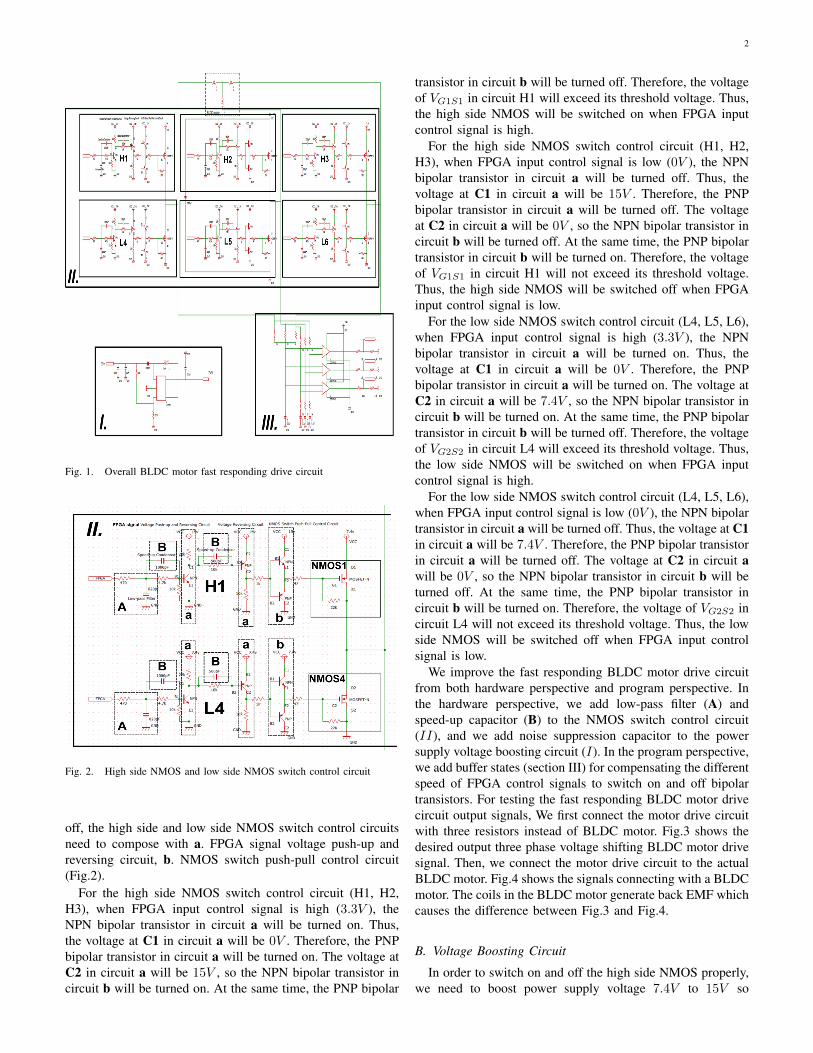
The fast responding BLDC motor drive circuit consistsof three primary functional circuits: I. power supply (7.4V )voltage boosting circuit [8],II. NMOS switch control circuit,III. rotor position sensor-less detection circuit [6]. Fig.1shows the overall fast responding BLDC motor drive circuit.The NMOS switch control circuit (II) is the central circuitin our fast responding BLDC motor drive circuity design. TheNMOS switch control circuit comprises three high side NMOSswitch control circuits(H1, H2, H3) and three low side NMOSswitch control circuits (L4, L5, L6).
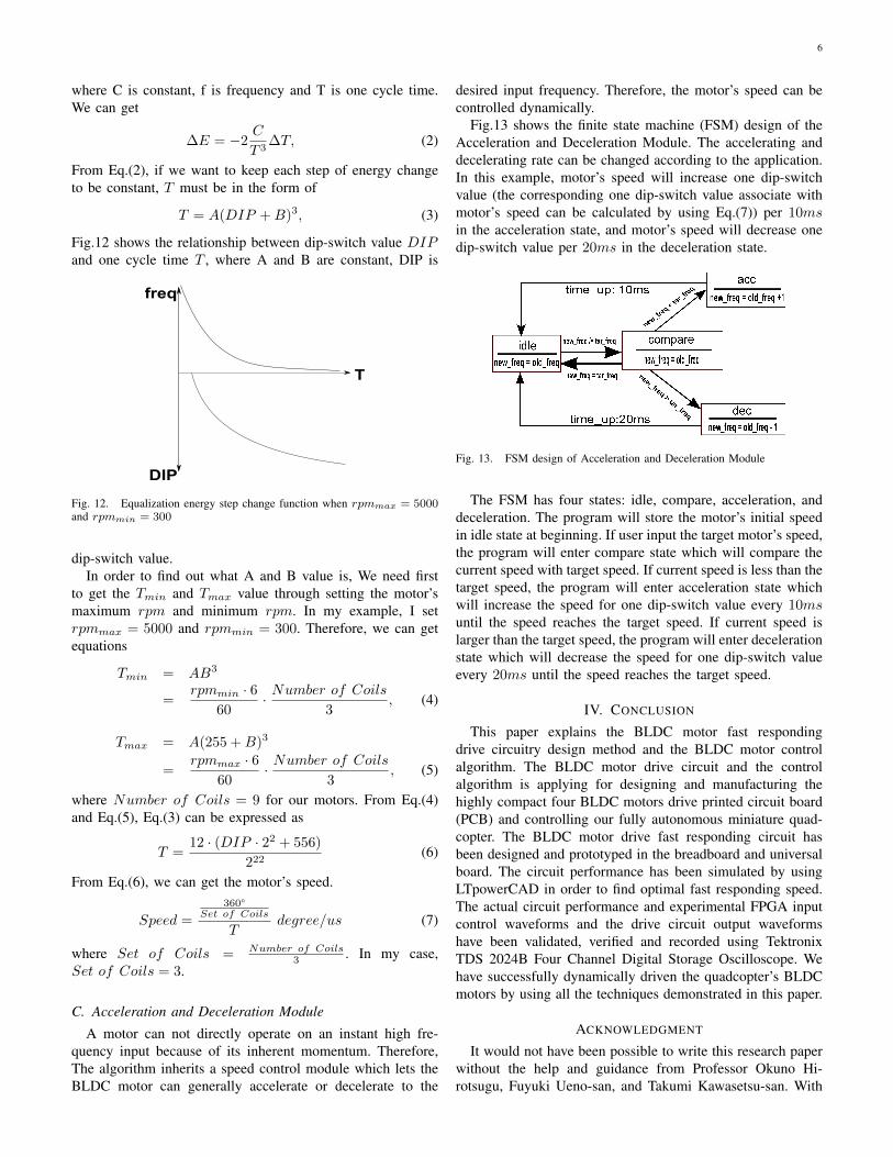
Applying NMOS guarantees a fast switch speed in thehardware perspective. The bipolar transistors in the high sideNMOS switch control circuits connect with high boostingvoltage (15V ). The bipolar transistors in the low side NMOSswitch control circuits connect with voltage power supply(7.4V ). Fig. 2 shows the detail design of the high side andlow side NMOS switch control circuit. In order to design afast and accurate responding BLDC Motor drive circuit, weapply low-pass filter (A in Fig.2) and speed-up capacitor (Bin Fig.2) techniques to eliminate the circuit noise and alleviateFPGA input control signals propagation delay time.
To switch the high side and low side NMOS on and offcorrespondingly with FPGA input signals, in other words,when FPGA input signal is high, NMOS will be switchedon, when FPGA input signal is low, NMOS will be switched
Fig. 1. Overall BLDC motor fast responding drive circuit
1
4
II.
aa b
A
B B
H
L
FPGA signal
a a b
A
B B
Fig. 2. High side NMOS and low side NMOS switch control circuit
off, the high side and low side NMOS switch control circuitsneed to compose with a. FPGA signal voltage push-up andreversing circuit, b. NMOS switch push-pull control circuit(Fig.2).
For the high side NMOS switch control circuit (H1, H2,H3), when FPGA input control signal is high (3.3V ), theNPN bipolar transistor in circuit a will be turned on. Thus,the voltage at C1 in circuit a will be 0V . Therefore, the PNPbipolar transistor in circuit a will be turned on. The voltage atC2 in circuit a will be 15V , so the NPN bipolar transistor incircuit b will be turned on. At the same time, the PNP bipolar
transistor in circuit b will be turned off. Therefore, the voltageof VG1S1 in circuit H1 will exceed its threshold voltage. Thus,the high side NMOS will be switched on when FPGA inputcontrol signal is high.
For the high side NMOS switch control circuit (H1, H2,H3), when FPGA input control signal is low (0V ), the NPNbipolar transistor in circuit a will be turned off. Thus, thevoltage at C1 in circuit a will be 15V . Therefore, the PNPbipolar transistor in circuit a will be turned off. The voltageat C2 in circuit a will be 0V , so the NPN bipolar transistor incircuit b will be turned off. At the same time, the PNP bipolartransistor in circuit b will be turned on. Therefore, the voltageof VG1S1 in circuit H1 will not exceed its threshold voltage.Thus, the high side NMOS will be switched off when FPGAinput control signal is low.
For the low side NMOS switch control circuit (L4, L5, L6),when FPGA input control signal is high (3.3V ), the NPNbipolar transistor in circuit a will be turned on. Thus, thevoltage at C1 in circuit a will be 0V . Therefore, the PNPbipolar transistor in circuit a will be turned on. The voltage atC2 in circuit a will be 7.4V , so the NPN bipolar transistor incircuit b will be turned on. At the same time, the PNP bipolartransistor in circuit b will be turned off. Therefore, the voltageof VG2S2 in circuit L4 will exceed its threshold voltage. Thus,the low side NMOS will be switched on when FPGA inputcontrol signal is high.
For the low side NMOS switch control circuit (L4, L5, L6),when FPGA input control signal is low (0V ), the NPN bipolartransistor in circuit a will be turned off. Thus, the voltage at C1in circuit a will be 7.4V . Therefore, the PNP bipolar transistorin circuit a will be turned off. The voltage at C2 in circuit awill be 0V , so the NPN bipolar transistor in circuit b will beturned off. At the same time, the PNP bipolar transistor incircuit b will be turned on. Therefore, the voltage of VG2S2 incircuit L4 will not exceed its threshold voltage. Thus, the lowside NMOS will be switched off when FPGA input controlsignal is low.
We improve the fast responding BLDC motor drive circuitfrom both hardware perspective and program perspective. Inthe hardware perspective, we add low-pass filter (A) andspeed-up capacitor (B) to the NMOS switch control circuit(II), and we add noise suppression capacitor to the powersupply voltage boosting circuit (I). In the program perspective,we add buffer states (section III) for compensating the differentspeed of FPGA control signals to switch on and off bipolartransistors. For testing the fast responding BLDC motor drivecircuit output signals, We first connect the motor drive circuitwith three resistors instead of BLDC motor. Fig.3 shows thedesired output three phase voltage shifting BLDC motor drivesignal. Then, we connect the motor drive circuit to the actualBLDC motor. Fig.4 shows the signals connecting with a BLDCmotor. The coils in the BLDC motor generate back EMF whichcauses the difference between Fig.3 and Fig.4.
B. Voltage Boosting Circuit
In order to switch on and off the high side NMOS properly,we need to boost power supply voltage 7.4V to 15V so
3
-2 0 2 4 6 8
Time[ms]
0
2
4
6
8
10
Voltage[V]
Phase One
-2 0 2 4 6 8
Time [ms]
-2
0
2
4
6
8
10
Voltage [
V]
Phase Two
-2 0 2 4 6 8
Time [ms]
-2
0
2
4
6
8
10
Voltage [
V]
Phase Three
Fig. 3. Output motor drive signals with buffer states connecting to resistors
that we can have the situation that VGS in the high sideNMOS switch control circuit exceeds the overdrive voltageto switch on the high side NMOS. We implement and modifyLM2733 application circuit ( see [8] for review) to fit into ourfast responding motor drive circuit. Fig.5 shows the modifiedversion of voltage boosting circuit in our motor drive circuit.In our application, we don’t need to control SHDN [8]. Thus,we connect VIN with SHDN [8]. Therefore, R3 [8] can beomitted. We also omit Cf [8] and add a noise suppressioncapacitor 100µF to stabilize 15V output voltage.
C. Low-pass Filter and Speed-up Capacitor
The NPN and PNP bipolar transistor are very sensitive tothe FPGA control signal noise. Some noise will exceed VBE
threshold voltage 0.7V , so the noise will turn the bipolartransistors on at undesired time, which will cause NMOS tobe switched on at improper time. The low-pass filter (A inFig.2) technique can eliminate the signal noise to get rid ofthe situation described above.
The speed-up capacitor (B in Fig.2) will tremendouslyincrease the discharging speed of the capacitors in NPN
0 20 40 60 80 100 120
Time [ms]
-1
0
1
2
3
4
5
6
Voltage [
V]
Phase One
0 20 40 60 80 100 120
Time [ms]
-1
0
1
2
3
4
5
6
Voltage [
V]
Phase Two
0 20 40 60 80 100 120
Time [ms]
-1
0
1
2
3
4
5
6
Voltage [
V]
Phase Three
Fig. 4. Output motor drive signals with buffer states connecting to BLDCmotor
Fig. 5. Voltage boosting circuit
4
bipolar transistors and PNP bipolar transistors (circuit a inFig.2) so that we can achieve to control FPGA input signals’rising edges’ delay time within 200ns and FPGA input signals’falling edges’ delay time within 3µs. Fig.6 shows the NMOS1(Fig.2) responding signal to FPGA input signal. Fig.7 showsthe NMOS4 (Fig.2) responding signal to FPGA input signal.
-0.0015 -0.001 -0.0005 0 0.0005 0.001 0.0015
Time[ms]
-5
0
5
10
15
20
Voltage [
V]
NMOS1 Responding Signal Rising Edge
FPGA Inpout Signal
-0.006 -0.004 -0.002 0 0.002 0.004 0.006
-5
0
5
10
15
Voltage [
V]
NMOS1 Responding Signal Falling Edge
FPGA Input Signal
Fig. 6. NMOS1 responding signal to FPGA input signal
D. Sensor-less BLDC Motor Rotor Position Detection Circuit
The BLDC motor used on our quadcopter is a small outerrotating magnet type BLDC motor. Fig.8 shows the motorinstalled on our quadcopter. Therefore, we implement a sensor-less rotor position detection circuit (see [6] for review) tofit into our application. Fig.9 shows the modified sensor-less BLDC motor rotor position detection circuit. The sensor-less BLDC motor rotor position detection circuit appliesback electromotive force (EMF) detection method to decidethe rotor position [6], which provides feedback motor speedinformation (state1, state2 and state3 in Fig.9) to the motorcontrol algorithm. In order to protect FPGA, we use voltagedivider in circuit C (Fig.9) for providing 3V to 4V feedbackvoltage to FPGA.
III. BLDC MOTOR CONTROL ALGORITHM
A. FPGA Input Signals
FPGA will generate six control signals to switch on andoff six corresponding NMOS in a particular order and timingfor the sake of generating BLDC motor three phase voltage
-0.0006 -0.0004 -0.0002 0 0.0002 0.0004 0.0006
Time [ms]
-2
0
2
4
6
8
Voltage [
V]
NMOS4 Responding Signal Rising Edge
FPGA Input signal
-0.006 -0.004 -0.002 0 0.002 0.004 0.006
Time [ms]
-4
-2
0
2
4
6
8
10
Voltage [
V]
NMOS4 Responding Signal Falling Edge
FPGA Input Signal
Fig. 7. NMOS4 responding signal to FPGA input signal
Fig. 8. LoutsRC C1803-1900KV BLDC motor
shifting control signals. Fig.10 (a) shows the diagram of FPGAswitching six NMOS . Fig.10 (b) shows the correspondingFPGA input control signals. Fig.10 (c) shows BLDC motorthree phase voltage shifting control signals. When FPGA inputcontrol signal is high (3.3V ), the NMOS will switch on. WhenFPGA input control signal is low (0V ), the NMOS will switchoff.
There are six states for forming the particular switchingorder. In state one (s1), NMOS one and six will be switchedon, and other NMOS will be switched off. In state two (s2),NMOS two and six will be switched on, and other NMOSwill be switched off. In state three (s3), NMOS two and fourwill be switched on, and other NMOS will be switched off.
5
Fig. 9. Sensor-less BLDC motor rotor position detection circuit
Fig. 10. (a) Motor control circuit diagram by implementing FPGA. PowerSupply V CC = 7.4V (b) FPGA input control signals. (c) Motor drive circuitoutput BLDC motor three phase voltage shifting control signals.
In state four (s4), NMOS three and four will be switchedon, and other NMOS will be switched off. In state five (s5),NMOS three and five will be switched on, and other NMOSwill be switched off. In state six (s6), NMOS one and five willbe switched on, and other NMOS will be switched off. Onecycle consists of these six states. One cycling time decides themotor’s speed.
If we keep sending the FPGA control signals (Fig.10(b)),we are able to generate the BLDC motor three phase voltageshifting control signals (Fig.10(c)). For example, in state one,NMOS one and six will be switched on. Therefore, in stateone, coil a is connecting to power supply (7.4V ). Coil c isconnecting to the ground (0V ). Coil b is in between coil aand coil c, so the voltage at coil b is half of coil a and coilc (3.7V ). The rest states can be analyzed in the same manneras in the state one. Thus, we are able to generate the BLDCmotor three phase voltage shifting control signals in Fig.10(c)by input the FPGA control signals in Fig.10(b).
In the actual FPGA input signals, we add extra 10us bufferstate between each state, which will switch all the NMOS off.In the actual motor drive circuit, there is a delay time whenFPGA input signals’ rising edges and falling edges acting onthe NMOS, which means the NMOS will not immediately tobe switched on or off when FPGA input signals’ rising edgesand falling edges occurring. The delay time of FPGA inputsignals’ rising edges are shorter than FPGA input signals’falling edges. Because of the different rising edges and fallingedges’ delay time, undesired noises will add into the finaloutput motor drive signals. In order to compensate the noises,we add extra six 10us buffer state between each state, so weimprove the motor drive circuit’s fast response performancein both program perspective and hardware perspective. Fig.11shows the FPGA input signals with 10us buffer states.
Fig. 11. FPGA input signals with 10us buffer states
B. Equalization Energy Step Change Function
The motor’s speed is controlled by eight bits dip-switch val-ues. We designed an equalization energy function associatingwith the dip-switch values in the BLDC motor control algo-rithm which makes FPGA provides uniform energy changein each step of acceleration and deceleration. From energyequation,
E = Cf2 =C
T 2, (1)
6
where C is constant, f is frequency and T is one cycle time.We can get
∆E = −2C
T 3∆T, (2)
From Eq.(2), if we want to keep each step of energy changeto be constant, T must be in the form of
T = A(DIP +B)3, (3)
Fig.12 shows the relationship between dip-switch value DIPand one cycle time T , where A and B are constant, DIP is
T
freq
DIP
Fig. 12. Equalization energy step change function when rpmmax = 5000and rpmmin = 300
dip-switch value.In order to find out what A and B value is, We need first
to get the Tmin and Tmax value through setting the motor’smaximum rpm and minimum rpm. In my example, I setrpmmax = 5000 and rpmmin = 300. Therefore, we can getequations
Tmin = AB3
=rpmmin · 6
60· Number of Coils
3, (4)
Tmax = A(255 +B)3
=rpmmax · 6
60· Number of Coils
3, (5)
where Number of Coils = 9 for our motors. From Eq.(4)and Eq.(5), Eq.(3) can be expressed as
T =12 · (DIP · 22 + 556)
222(6)
From Eq.(6), we can get the motor’s speed.
Speed =
360°Set of Coils
Tdegree/us (7)
where Set of Coils = Number of Coils3 . In my case,
Set of Coils = 3.
C. Acceleration and Deceleration Module
A motor can not directly operate on an instant high fre-quency input because of its inherent momentum. Therefore,The algorithm inherits a speed control module which lets theBLDC motor can generally accelerate or decelerate to the
desired input frequency. Therefore, the motor’s speed can becontrolled dynamically.
Fig.13 shows the finite state machine (FSM) design of theAcceleration and Deceleration Module. The accelerating anddecelerating rate can be changed according to the application.In this example, motor’s speed will increase one dip-switchvalue (the corresponding one dip-switch value associate withmotor’s speed can be calculated by using Eq.(7)) per 10msin the acceleration state, and motor’s speed will decrease onedip-switch value per 20ms in the deceleration state.
acc
idlecompare
dec
new_freq <
tar_
freq
new_freq > tar_freq
new_freq /= tar_freq
time_up: 10ms
time_up:20msnew_freq = old_freq - 1
new_freq = old_freq +1
new_freq = old_freq new_freq = old_freq
Fig. 13. FSM design of Acceleration and Deceleration Module
The FSM has four states: idle, compare, acceleration, anddeceleration. The program will store the motor’s initial speedin idle state at beginning. If user input the target motor’s speed,the program will enter compare state which will compare thecurrent speed with target speed. If current speed is less than thetarget speed, the program will enter acceleration state whichwill increase the speed for one dip-switch value every 10msuntil the speed reaches the target speed. If current speed islarger than the target speed, the program will enter decelerationstate which will decrease the speed for one dip-switch valueevery 20ms until the speed reaches the target speed.
IV. CONCLUSION
This paper explains the BLDC motor fast respondingdrive circuitry design method and the BLDC motor controlalgorithm. The BLDC motor drive circuit and the controlalgorithm is applying for designing and manufacturing thehighly compact four BLDC motors drive printed circuit board(PCB) and controlling our fully autonomous miniature quad-copter. The BLDC motor drive fast responding circuit hasbeen designed and prototyped in the breadboard and universalboard. The circuit performance has been simulated by usingLTpowerCAD in order to find optimal fast responding speed.The actual circuit performance and experimental FPGA inputcontrol waveforms and the drive circuit output waveformshave been validated, verified and recorded using TektronixTDS 2024B Four Channel Digital Storage Oscilloscope. Wehave successfully dynamically driven the quadcopter’s BLDCmotors by using all the techniques demonstrated in this paper.
ACKNOWLEDGMENT
It would not have been possible to write this research paperwithout the help and guidance from Professor Okuno Hi-rotsugu, Fuyuki Ueno-san, and Takumi Kawasetsu-san. With
7
their great help and critical thinking, this project can bepossible. They guide me through all the stages of this re-search. Their advises and supports are precious on both anacademic and personal level for which I am very grateful.This research project was carried out in Professor TetsuyaYagi’s Neurophysiology of Visualization Applied EngineeringSystems Laboratory for FrontierLab Research Program atOsaka University.
REFERENCES
[1] Amtel, "Sensorless control of 3-phase brushless DC motors" applicationnotes.
[2] Texas Instruments, "LM2733 0.6/1.6 MHz Boost Converters With 40VInternal FET Switch in SOT-23" application notes.
[3] M. Zoheb, V. Sharma M, S. Vashishtha and M. Shahid, "Implementationof Brushless DC Motor Using FPGA Interface", vol. 2, issue 5, May2013.
[4] V. A. Pedroni, Circuit Design and Simulation with VHDL. The MITPress, Cambridge, Massachusetts, September 17th, 2010.
[5] V. A. Pedroni, Finite State Machines in Hardware: Theory and Design(with VHDL and SystemVerilog). The MIT Press, Cambridge, Mas-sachusetts, December 20th, 2013.
[6] H.Onda, "Ultra-high speed and sensor-less drive system for smallbrushless-motor," Annals of Shizuoka Institute of Science and Technol-ogy., vol. 18, pp. 41–45, March 1st, 2010.