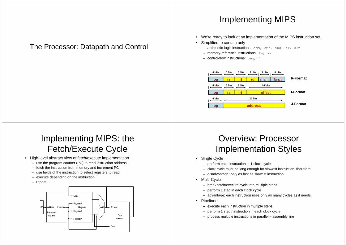
The Processor: Datapath and Control • We're ready to look at an implementation of the MIPS instruction set • Simplified to contain only – arithmetic-logic instructions: add, sub, and, or, slt – memory-reference instructions: lw, sw – control-flow instructions: beq, j Implementing MIPS op rs rt offset 6 bits 5 bits 5 bits 16 bits op rs rt rd funct shamt 6 bits 5 bits 5 bits 5 bits 5 bits 6 bits R-Format I-Format op address 6 bits 26 bits J-Format • High-level abstract view of fetch/execute implementation – use the program counter (PC) to read instruction address – fetch the instruction from memory and increment PC – use fields of the instruction to select registers to read – execute depending on the instruction – repeat… Implementing MIPS: the Fetch/Execute Cycle Registers Register # Data Register # Data memory Address Data Register # PC Instruction ALU Instruction memory Address Overview: Processor Implementation Styles • Single Cycle – perform each instruction in 1 clock cycle – clock cycle must be long enough for slowest instruction; therefore, – disadvantage: only as fast as slowest instruction • Multi-Cycle – break fetch/execute cycle into multiple steps – perform 1 step in each clock cycle – advantage: each instruction uses only as many cycles as it needs • Pipelined – execute each instruction in multiple steps – perform 1 step / instruction in each clock cycle – process multiple instructions in parallel – assembly line
Transcript
The Processor: Datapath and Control
• We're ready to look at an implementation of the MIPS instruction set• Simplified to contain only
• High-level abstract view of fetch/execute implementation– use the program counter (PC) to read instruction address– fetch the instruction from memory and increment PC– use fields of the instruction to select registers to read– execute depending on the instruction– repeat…
Implementing MIPS: the Fetch/Execute Cycle
Registers
Register #
Data
Register #
Data memory
Address
Data
Register #
PC Instruction ALU
Instruction memory
Address
Overview: Processor Implementation Styles
• Single Cycle– perform each instruction in 1 clock cycle
– clock cycle must be long enough for slowest instruction; therefore,– disadvantage: only as fast as slowest instruction
• Multi-Cycle– break fetch/execute cycle into multiple steps
– perform 1 step in each clock cycle
– advantage: each instruction uses only as many cycles as it needs
• Pipelined– execute each instruction in multiple steps
– perform 1 step / instruction in each clock cycle– process multiple instructions in parallel – assembly line
• Two types of functional elements in the hardware:– elements that operate on data (called combinational elements)
– elements that contain data (called state or sequential elements)
Functional Elements Combinational Elements
• Works as an input ⇒ output function, e.g., ALU• Combinational logic reads input data from one register and writes
output data to another, or same, register– read/write happens in a single cycle – combinational element cannot
store data from one cycle to a future one
Clock cycle
State element
1Combinational logic
State element
2
State element
Combinational logic
Combinational logic hardware units
State Elements
• State elements contain data in internal storage, e.g., registersand memory
• All state elements together define the state of the machine– What does this mean? Think of shutting down and starting up again…
• Flipflops and latches are 1-bit state elements, equivalently, they are 1-bit memories
• The output(s) of a flipflop or latch always depends on the bit value stored, i.e., its state, and can be called 1/0 or high/low or true/false
• The input to a flipflop or latch can change its state depending on whether it is clocked or not…
• Clocks are used in synchronous logic to determine when a state element is to be updated – in level-triggered clocking methodology either the state changes
only when the clock is high or only when it is low (technology-dependent)
– in edge-triggered clocking methodology either the rising edge or falling edge is active (depending on technology) – i.e., states change only on rising edges or only on falling edge
• Latches are level-triggered• Flipflops are edge-triggered
Synchronous Logic: Clocked Latches and Flipflops
Clock period Rising edge
Falling edge
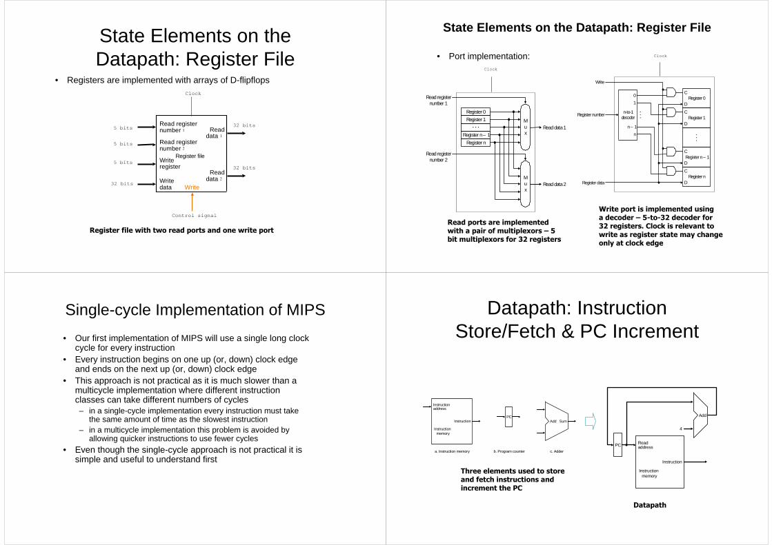
• Registers are implemented with arrays of D-flipflops
State Elements on the Datapath: Register File
Register file with two read ports and one write port
Clock
5 bits
5 bits
5 bits
32 bits
32 bits
32 bits
Control signal
Read registernumber 1 Read
data 1
Readdata 2
Read registernumber 2
Register fileWriteregister
Writedata Write
• Port implementation:
Read ports are implemented with a pair of multiplexors – 5 bit multiplexors for 32 registers
Write port is implemented usinga decoder – 5-to-32 decoder for32 registers. Clock is relevant to write as register state may change only at clock edge
M u x
Register 0
Register 1
Register n – 1
Register n
M u x
Read data 1
Read data 2
Read register number 1
Read register number 2
Clock
n-to-1 decoder
Register 0
Register 1
Register n – 1C
C
D
DRegister n
C
C
D
D
Register number
Write
Register data
0
1
n – 1
n
Clock
State Elements on the Datapath: Register File
Single-cycle Implementation of MIPS
• Our first implementation of MIPS will use a single long clock cycle for every instruction
• Every instruction begins on one up (or, down) clock edge and ends on the next up (or, down) clock edge
• This approach is not practical as it is much slower than a multicycle implementation where different instruction classes can take different numbers of cycles– in a single-cycle implementation every instruction must take
the same amount of time as the slowest instruction– in a multicycle implementation this problem is avoided by
allowing quicker instructions to use fewer cycles
• Even though the single-cycle approach is not practical it is simple and useful to understand first
Datapath: Instruction Store/Fetch & PC Increment
PC
Instruction memory
Instruction address
Instruction
a. Instruction memory b. Program counter
Add Sum
c. Adder
PC
Instruction memory
Read address
Instruction
4
Add
Three elements used to store and fetch instructions andincrement the PC
Datapath
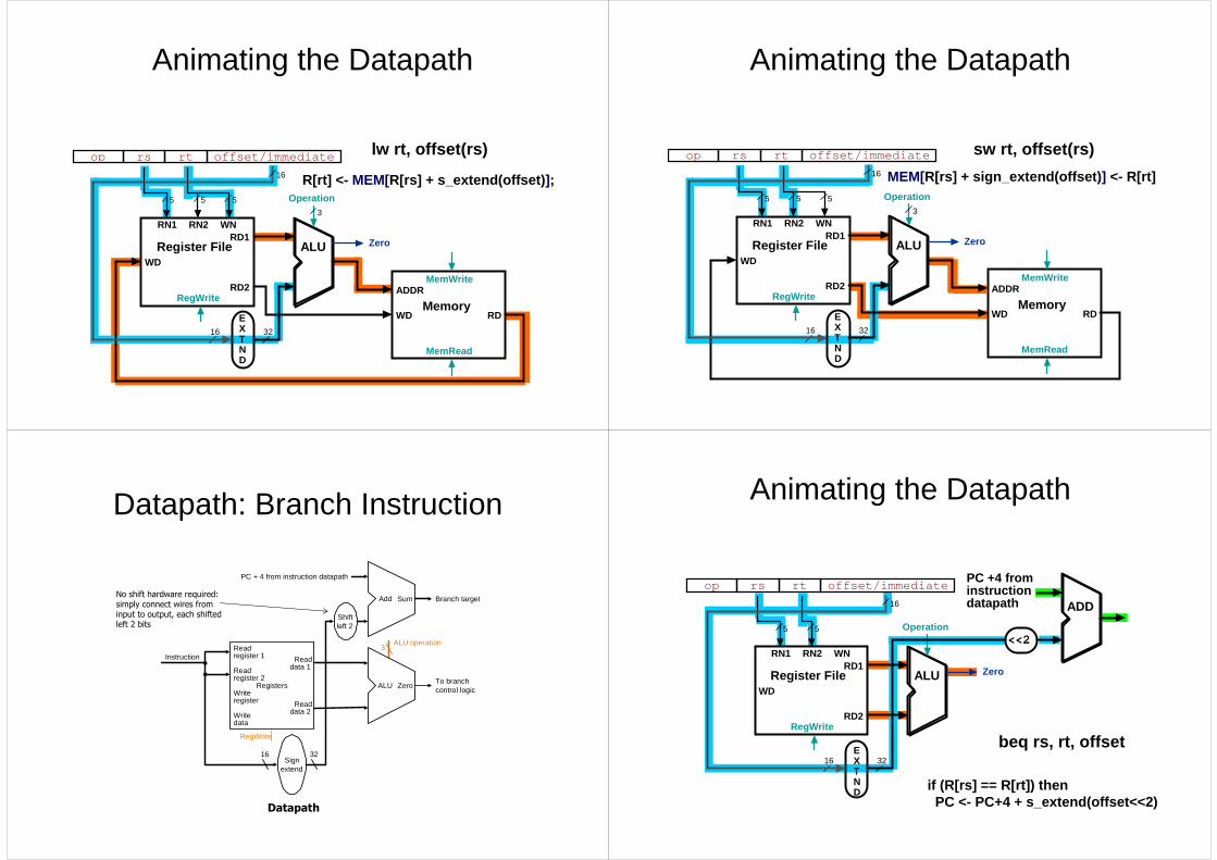
Animating the Datapath
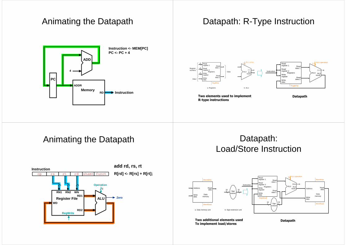
Instruction <- MEM[PC]PC <- PC + 4
RDMemory
ADDR
PC
Instruction
4
ADD
Datapath: R-Type Instruction
ALU control
RegWrite
RegistersWrite register
Read data 1
Read data 2
Read register 1
Read register 2
Write data
ALU result
ALU
Data
Data
Register numbers
a. Registers b. ALU
Zero5
5
5 3
InstructionRegisters
Write register
Read data 1
Read data 2
Read register 1
Read register 2
Write data
ALU result
ALU
Zero
RegWrite
ALU operation3
Two elements used to implementR-type instructions
Datapath
Animating the Datapath
add rd, rs, rt
R[rd] <- R[rs] + R[rt];
5 5 5
RD1
RD2
RN1 RN2 WN
WD
RegWrite
Register File
op rs rt rd functshamt
Operation
ALU Zero
Instruction
3
Datapath: Load/Store Instruction
16 32Sign
extend
b. Sign-extension unit
MemRead
MemWrite
Data memory
Write data
Read data
a. Data memory unit
Address
Instruction
16 32
RegistersWrite register
Read data 1
Read data 2
Read register 1
Read register 2
Data memory
Write data
Read data
Write data
Sign extend
ALU result
ZeroALU
Address
MemRead
MemWrite
RegWrite
ALU operation3
Two additional elements usedTo implement load/stores
Datapath
Animating the Datapath
op rs rt offset/immediate
5 5
16
RD1
RD2
RN1 RN2 WN
WD
RegWrite
Register File
Operation
ALU
3
EXTND
16 32
Zero
RDWD
MemRead
MemoryADDR
MemWrite
5
lw rt, offset(rs)
R[rt] <- MEM[R[rs] + s_extend(offset)];
Animating the Datapath
op rs rt offset/immediate
5 5
16
RD1
RD2
RN1 RN2 WN
WD
RegWrite
Register File
Operation
ALU
3
EXTND
16 32
Zero
RDWD
MemRead
MemoryADDR
MemWrite
5
sw rt, offset(rs)
MEM[R[rs] + sign_extend(offset)] <- R[rt]
Datapath: Branch Instruction
16 32Sign
extend
ZeroALU
Sum
Shift left 2
To branch control logic
Branch target
PC + 4 from instruction datapath
Instruction
Add
RegistersWrite register
Read data 1
Read data 2
Read register 1
Read register 2
Write data
RegWrite
ALU operation3
Datapath
No shift hardware required:simply connect wires from input to output, each shiftedleft 2 bits
Animating the Datapath
beq rs, rt, offset
if (R[rs] == R[rt]) then PC <- PC+4 + s_extend(offset<<2)
op rs rt offset/immediate
5 5
16
RD1
RD2
RN1 RN2 WN
WD
RegWrite
Register File
Operation
ALU
EXTND
16 32
Zero
ADD
<<2
PC +4 from instruction datapath
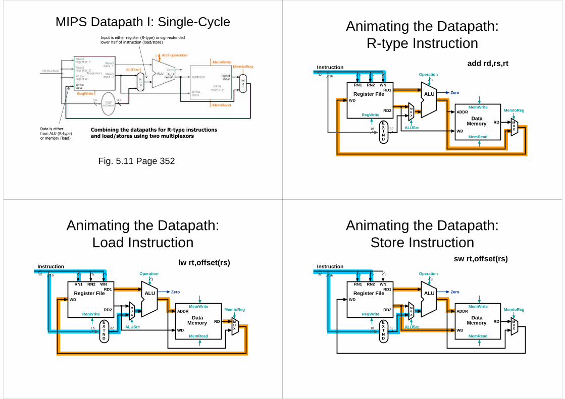
MIPS Datapath I: Single-CycleInput is either register (R-type) or sign-extendedlower half of instruction (load/store)
Combining the datapaths for R-type instructions and load/stores using two multiplexors
Data is either from ALU (R-type)or memory (load)
Fig. 5.11 Page 352
Animating the Datapath: R-type Instruction
add rd,rs,rt5 516
RD1
RD2
RN1 RN2 WN
WD
RegWrite
Register File
Operation
ALU
3
EXTND
16 32
Zero
RD
WDMemRead
DataMemory
ADDRMemWrite
5
Instruction32
MUX
MUXALUSrc
MemtoReg
Animating the Datapath: Load Instruction
lw rt,offset(rs)5 516
RD1
RD2
RN1 RN2 WN
WD
RegWrite
Register File
Operation
ALU
3
EXTND
16 32
Zero
RD
WDMemRead
DataMemory
ADDRMemWrite
5
Instruction32
MUX
MUXALUSrc
MemtoReg
Animating the Datapath: Store Instruction
sw rt,offset(rs)
5 516
RD1
RD2
RN1 RN2 WN
WD
RegWrite
Register File
Operation
ALU
3
EXTND
16 32
Zero
RD
WDMemRead
DataMemory
ADDRMemWrite
5
Instruction32
MUX
MUXALUSrc
MemtoReg
MIPS Datapath II: Single-Cycle
PC
Instruction memory
Read address
Instruction
16 32
Registers
Write register
Write data
Read data 1
Read data 2
Read register 1
Read register 2
Sign extend
ALU result
Zero
Data memory
Address
Write data
Read data M
u x
4
Add
M u x
ALU
RegWrite
ALU operation3
MemRead
MemWrite
ALUSrcMemtoReg
Adding instruction fetch
Separate instruction memoryas instruction and data readoccur in the same clock cycle
Separate adder as ALU operations and PC increment occur in the same clock cycle
MIPS Datapath III: Single-Cycle
PC
Instruction memory
Read address
Instruction
16 32
Add ALU result
M u x
Registers
Write registerWrite data
Read data 1
Read data 2
Read register 1Read register 2
Shift left 2
4
M u x
ALU operation3
RegWrite
MemRead
MemWrite
PCSrc
ALUSrc
MemtoReg
ALU result
ZeroALU
Data memory
Address
Write data
Read data M
u x
Sign extend
Add
Adding branch capability and another multiplexor
Instruction address is eitherPC+4 or branch target address
Extra adder needed as bothadders operate in each cycle
New multiplexor
Important note: in a single-cycle implementation data cannot be stored during an instruction – it only moves through combinational logicQuestion: is the MemRead signal really needed?! Think of RegWrite…!
5 516
RD1
RD2
RN1 RN2 WN
WD
RegWrite
Register File
Operation
ALU
3
EXTND
16 32
Zero
RD
WDMemRead
DataMemory
ADDRMemWrite
5
Instruction32
MUX
ALUSrc
MemtoReg
ADD
<<2
RD
InstructionMemory
ADDR
PC
4
ADD
ADD
MUX
MUX
PCSrc
Datapath Executing addadd rd, rs, rt
5 516
RD1
RD2
RN1 RN2 WN
WD
RegWrite
Register File
Operation
ALU
3
EXTND
16 32
Zero
RD
WDMemRead
DataMemory
ADDRMemWrite
5
Instruction32
MUX
ALUSrc
MemtoReg
ADD
<<2
RD
InstructionMemory
ADDR
PC
4
ADD
ADD
MUX
MUX
PCSrc
Datapath Executing lwlw rt,offset(rs)
5 516
RD1
RD2
RN1 RN2 WN
WD
RegWrite
Register File
Operation
ALU
3
EXTND
16 32
Zero
RD
WDMemRead
DataMemory
ADDRMemWrite
5
Instruction32
MUX
ALUSrc
MemtoReg
ADD
<<2
RD
InstructionMemory
ADDR
PC
4
ADD
ADD
MUX
MUX
PCSrc
Datapath Executing swsw rt,offset(rs)
5 516
RD1
RD2
RN1 RN2 WN
WD
RegWrite
Register File
Operation
ALU
3
EXTND
16 32
Zero
RD
WDMemRead
DataMemory
ADDRMemWrite
5
Instruction32
MUX
ALUSrc
MemtoReg
ADD
<<2
RD
InstructionMemory
ADDR
PC
4
ADD
ADD
MUX
MUX
PCSrc
Datapath Executing beqbeq r1,r2,offset
Control
• Control unit takes input from– the instruction opcode bits
• Control unit generates– ALU control input– write enable (possibly, read enable also) signals for each storage
element– selector controls for each multiplexor
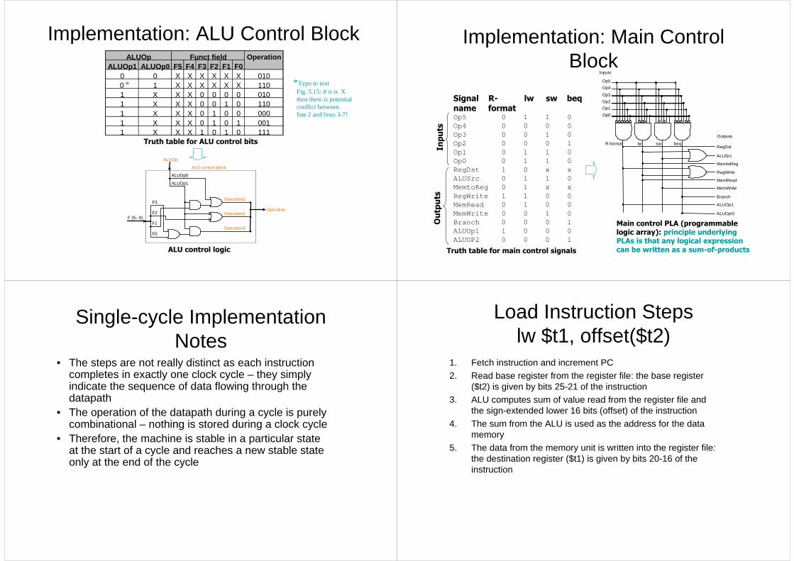
ALU Control
• Plan to control ALU: main control sends a 2-bit ALUOp control field to the ALU control. Based on ALUOp and funct field of instruction the ALU control generates the 3-bit ALU control field
– ALU control Func-field tion
000 and001 or010 add110 sub111 slt
• ALU must perform– add for load/stores (ALUOp 00)– sub for branches (ALUOp 01)– one of and, or, add, sub, slt for R-type instructions, depending on the
instruction’s 6-bit funct field (ALUOp 10)
MainControl
ALUControl
2
ALUOp
6
Instructionfunct field
3
ALU controlinput
ToALU
ALUOp generationby main control
Recall from Ch. 4
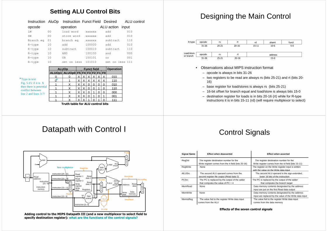
Setting ALU Control Bits
Instruction AluOp Instruction Funct Field Desired ALU controlopcode operation ALU action inputLW 00 load word xxxxxx add 0 10
SW 00 store word xxxxxx add 0 10
Branch eq 01 branch eq xxxxxx subtract 110
R-type 10 add 100000 add 010
R-type 10 subtract 100010 subtract 110
R-type 10 AND 100100 and 000
R-type 10 OR 100101 or 001
R-type 10 set on less 101010 set on l ess 111
Truth table for ALU control bits
ALUOp Funct field OperationALUOp1 ALUOp0 F5 F4 F3 F2 F1 F0
0 0 X X X X X X 0100 1 X X X X X X 1101 X X X 0 0 0 0 0101 X X X 0 0 1 0 1101 X X X 0 1 0 0 0001 X X X 0 1 0 1 0011 X X X 1 0 1 0 111
**Typo in text Fig. 5.15: if it is X then there is potential conflict between line 2 and lines 3-7!
Designing the Main Control
• Observations about MIPS instruction format– opcode is always in bits 31-26
– two registers to be read are always rs (bits 25-21) and rt (bits 20-16)
– base register for load/stores is always rs (bits 25-21)
– 16-bit offset for branch equal and load/store is always bits 15-0
– destination register for loads is in bits 20-16 (rt) while for R-type instructions it is in bits 15-11 (rd) (will require multiplexor to select)
31-26 25-21 20-16 15-11 10-6 5-0
31-26 25-21 20-16 15-0
opcode
opcode
rs
rs
rt
rt address
rd shamt functR-type
Load/store or branch
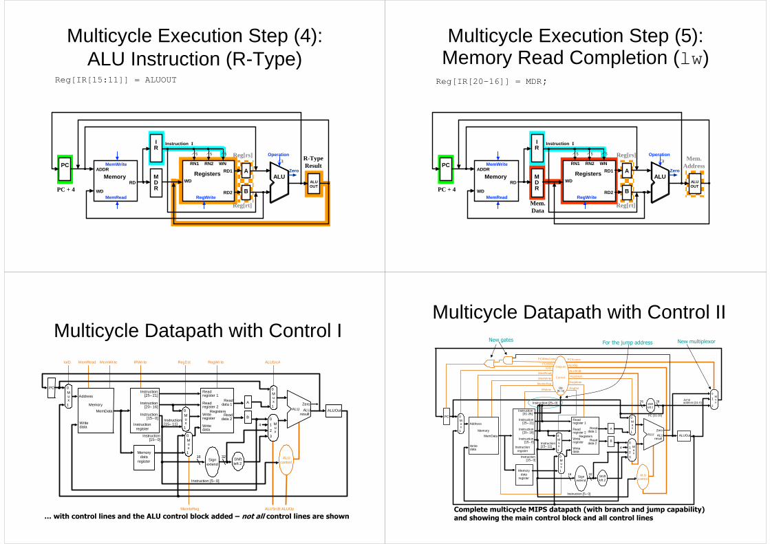
Datapath with Control I
MemtoReg
MemRead
MemWrite
ALUOp
ALUSrc
RegDst
PC
Instruction memory
Read address
Instruction [31– 0]
Instruction [20– 16]
Instruction [25– 21]
Add
Instruction [5– 0]
RegWrite
4
16 32Instruction [15– 0]
0Registers
Write registerWrite data
Write data
Read data 1
Read data 2
Read register 1Read register 2
Sign extend
ALU result
Zero
Data memory
Address Read data M
u x
1
0
M u x
1
0
M u x
1
0
M u x
1
Instruction [15– 11]
ALU control
Shift left 2
PCSrc
ALU
Add ALU result
Adding control to the MIPS Datapath III (and a new multiplexor to select field to specify destination register): what are the functions of the control signals?
New multiplexor
Control Signals
Signal Name Effect when deasserted Effect when asserted
RegDst The register destination number for the The register destination number for theWrite register comes from the rt field (bits 20-16) Write register comes from the rd field (bits 15-11)
RegWrite None The register on the Write register input is written with the value on the Write data input
AlLUSrc The second ALU operand comes from the The second ALU operand is the sign-extended, second register file output (Read data 2) lower 16 bits of the instruction
PCSrc The PC is replaced by the output of the adder The PC is replaced by the output of the adderthat computes the value of PC + 4 that computes the branch target
MemRead None Data memory contents designated by the addressinput are put on the first Read data output
MemWrite None Data memory contents designated by the addressinput are replaced by the value of the Write data input
MemtoReg The value fed to the register Write data input The value fed to the register Write data inputcomes from the ALU comes from the data memory
Effects of the seven control signals
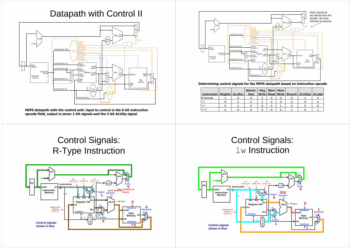
Datapath with Control II
PC
Instruction memory
Read address
Instruction [31–0]
Instruction [20 16]
Instruction [25 21]
Add
Instruction [5 0]
MemtoReg
ALUOp
MemWrite
RegWrite
MemRead
BranchRegDst
ALUSrc
Instruction [31 26]
4
16 32Instruction [15 0]
0
0M u x
0
1
Control
Add ALU result
M u x
0
1
RegistersWrite register
Write data
Read data 1
Read data 2
Read register 1
Read register 2
Sign extend
M u x
1
ALU result
Zero
PCSrc
Data memory
Write data
Read data
M u x
1
Instruction [15 11]
ALU control
Shift left 2
ALUAddress
MIPS datapath with the control unit: input to control is the 6-bit instructionopcode field, output is seven 1-bit signals and the 2-bit ALUOp signal
Instruction RegDst ALUSrcMemto-
RegReg
WriteMem Read
Mem Write Branch ALUOp1 ALUp0
R-format 1 0 0 1 0 0 0 1 0lw 0 1 1 1 1 0 0 0 0sw X 1 X 0 0 1 0 0 0beq X 0 X 0 0 0 1 0 1
PC
Instruction memory
Read address
Instruction [31– 0]
Instruction [20 16]
Instruction [25 21]
Add
Instruction [5 0]
MemtoReg
ALUOp
MemWrite
RegWrite
MemRead
BranchRegDst
ALUSrc
Instruction [31 26]
4
16 32Instruction [15 0]
0
0M u x
0
1
Control
Add ALU result
M u x
0
1
RegistersWrite register
Write data
Read data 1
Read data 2
Read register 1
Read register 2
Sign extend
M u x
1
ALU result
Zero
PCSrc
Data memory
Write data
Read data
M u x
1
Instruction [15 11]
ALU control
Shift left 2
ALUAddress
Determining control signals for the MIPS datapath based on instruction opcode
PCSrc cannot beset directly from the opcode: zero test outcome is required
Control Signals:R-Type Instruction
Control signalsshown in blue
1
0
0
0
1
???Value depends on
funct
0
0
5 516
RD1
RD2
RN1 RN2 WN
WD
RegWrite
Register File
Operation
ALU
3
EXTND
16 32
Zero
RD
WDMemRead
DataMemory
ADDRMemWrite
5
Instruction I32
MUX
ALUSrc
MemtoReg
ADD
<<2
RD
InstructionMemory
ADDR
PC
4
ADD
ADD
MUX
MUX
PCSrc
MUX RegDst
5
rdI[15:11]
rtI[20:16]
rsI[25:21]
immediate/offsetI[15:0]
0
1
0
11
0
10
Control Signals:lw Instruction
0
Control signalsshown in blue
0010
1
1
1
0
1
5 516
RD1
RD2
RN1 RN2 WN
WD
RegWrite
Register File
Operation
ALU
3
EXTND
16 32
Zero
RD
WDMemRead
DataMemory
ADDRMemWrite
5
Instruction I32
MUX
ALUSrc
MemtoReg
ADD
<<2
RD
InstructionMemory
ADDR
PC
4
ADD
ADD
MUX
MUX
PCSrc
MUX RegDst
5
rdI[15:11]
rtI[20:16]
rsI[25:21]
immediate/offsetI[15:0]
0
1
0
11
0
10
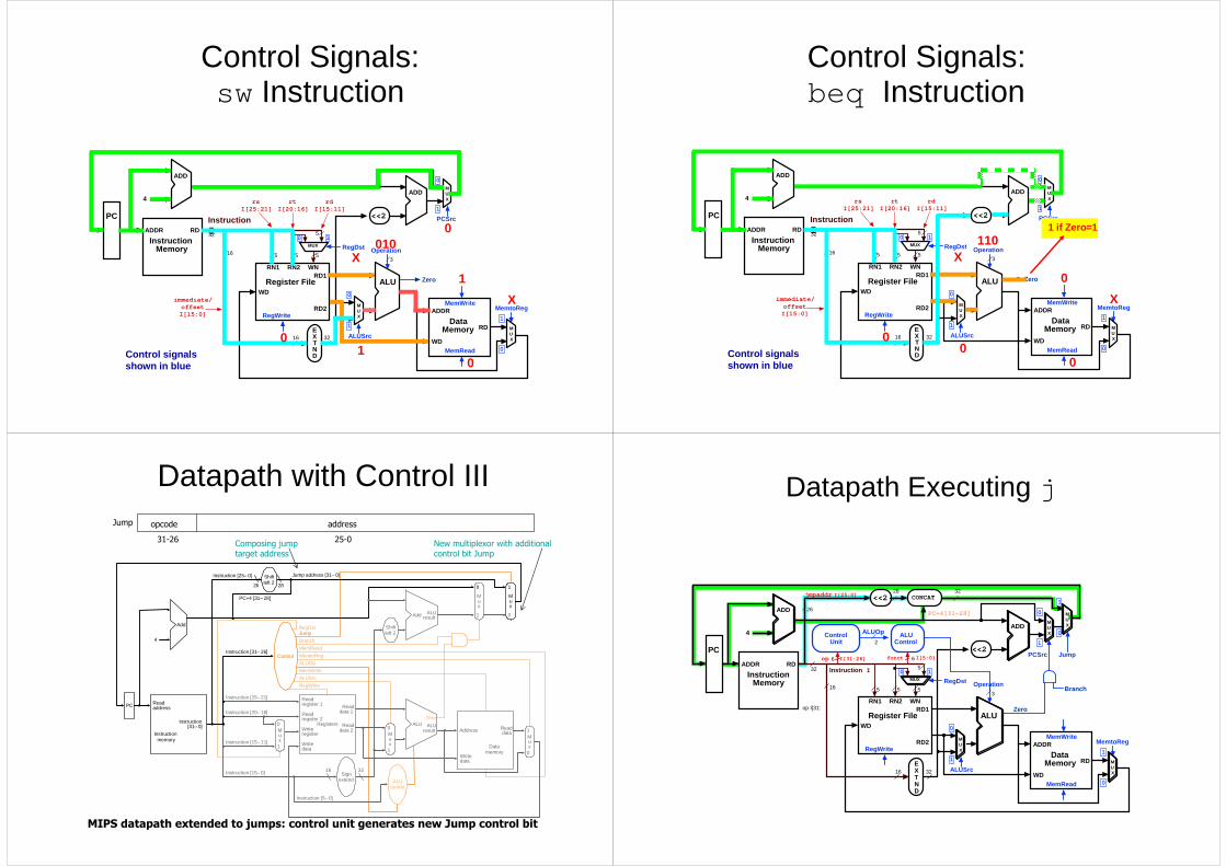
Control Signals:sw Instruction
0
Control signalsshown in blue
X010
1
X
0
1
0
5 516
RD1
RD2
RN1 RN2 WN
WD
RegWrite
Register File
Operation
ALU
3
EXTND
16 32
Zero
RD
WDMemRead
DataMemory
ADDRMemWrite
5
Instruction I32
MUX
ALUSrc
MemtoReg
ADD
<<2
RD
InstructionMemory
ADDR
PC
4
ADD
ADD
MUX
MUX
PCSrc
MUX RegDst
5
rdI[15:11]
rtI[20:16]
rsI[25:21]
immediate/offsetI[15:0]
0
1
0
11
0
10
Control Signals:beq Instruction
Control signalsshown in blue
X110
0
X
0
0
0
1 if Zero=1
Datapath with Control III
Shift left 2
PC
Instruction memory
Read address
Instruction [31– 0]
Data memory
Read data
Write data
RegistersWrite register
Write data
Read data 1
Read data 2
Read register 1
Read register 2
Instruction [15– 11]
Instruction [20– 16]
Instruction [25– 21]
Add
ALU result
Zero
Instruction [5– 0]
MemtoReg
ALUOp
MemWrite
RegWrite
MemRead
Branch
JumpRegDst
ALUSrc
Instruction [31– 26]
4
M u x
Instruction [25– 0] Jump address [31– 0]
PC+4 [31– 28]
Sign extend
16 32Instruction [15– 0]
1
M u x
1
0
M u x
0
1
M u x
0
1
ALU control
Control
Add ALU result
M u x
0
1 0
ALU
Shift left 226 28
Address
31-26 25-0
opcode addressJump
MIPS datapath extended to jumps: control unit generates new Jump control bit
Main control PLA (programmablelogic array): principle underlyingPLAs is that any logical expressioncan be written as a sum-of-products
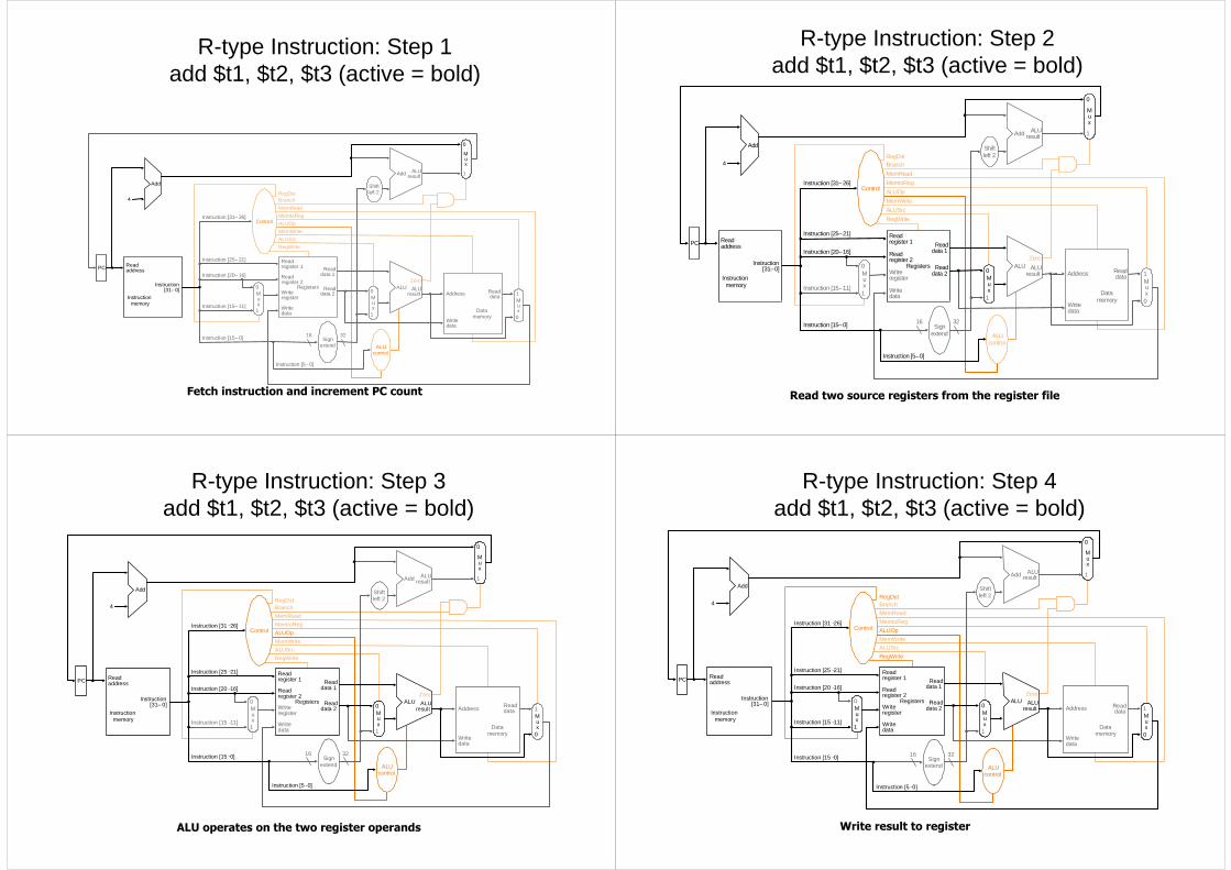
Single-cycle Implementation Notes
• The steps are not really distinct as each instruction completes in exactly one clock cycle – they simply indicate the sequence of data flowing through the datapath
• The operation of the datapath during a cycle is purely combinational – nothing is stored during a clock cycle
• Therefore, the machine is stable in a particular state at the start of a cycle and reaches a new stable state only at the end of the cycle
1. Fetch instruction and increment PC2. Read base register from the register file: the base register
($t2) is given by bits 25-21 of the instruction3. ALU computes sum of value read from the register file and
the sign-extended lower 16 bits (offset) of the instruction4. The sum from the ALU is used as the address for the data
memory5. The data from the memory unit is written into the register file:
the destination register ($t1) is given by bits 20-16 of the instruction
Load Instruction Stepslw $t1, offset($t2)
1. Fetch instruction and increment PC2. Read two register ($t1 and $t2) from the register file3. ALU performs a subtract on the data values from the
register file; the value of PC+4 is added to the sign-extended lower 16 bits (offset) of the instruction shifted left by two to give the branch target address
4. The Zero result from the ALU is used to decide which adder result (from step 1 or 3) to store in the PC
Branch Instruction Stepsbeq $t1, $t2, offset
• Assuming fixed-period clock every instruction datapath uses one clock cycle implies:
– CPI = 1
– cycle time determined by length of the longest instruction path (load)
• but several instructions could run in a shorter clock cycle: waste of time
• consider if we have more complicated instructions like floating point!
– resources used more than once in the same cycle need to be
duplicated
• waste of hardware and chip area
Single-Cycle Design Problems
Example: Fixed-period clock vs. variable-period clock in a
single-cycle implementation• Consider a machine with an additional floating point unit. Assume
functional unit delays as follows– memory: 2 ns., ALU and adders: 2 ns., FPU add: 8 ns., FPU multiply: 16 ns.,
register file access (read or write): 1 ns.– multiplexors, control unit, PC accesses, sign extension, wires: no delay
• Assume instruction mix as follows– all loads take same time and comprise 31%– all stores take same time and comprise 21% – R-format instructions comprise 27%– branches comprise 5%– jumps comprise 2%– FP adds and subtracts take the same time and totally comprise 7%– FP multiplys and divides take the same time and totally comprise 7%
• Compare the performance of (a) a single-cycle implementation using a fixed-period clock with (b) one using a variable-period clock where each instruction executes in one clock cycle that is only as long as it needs to be (not really practical but pretend it’s possible!)
Solution
• Clock period for fixed-period clock = longest instruction time = 20 ns.
• Average clock period for variable-period clock = 8 × 31% +7 × 21% + 6 × 27% + 5 × 5% + 2 × 2% + 20 × 7% + 12 × 7% = 7.0 ns.
• One solution: a variable-period clock with different cycle times for each instruction class– unfeasible, as implementing a variable-speed clock is technically
difficult
• Another solution:– use a smaller cycle time…
– …have different instructions take different numbers of cycles
by breaking instructions into steps and fitting each step into one cycle
– feasible: multicyle approach!
• Break up the instructions into steps– each step takes one clock cycle– balance the amount of work to be done in each step/cycle so that
they are about equal– restrict each cycle to use at most once each major functional unit
so that such units do not have to be replicated– functional units can be shared between different cycles within one
instruction
• Between steps/cycles– At the end of one cycle store data to be used in later cycles of the
same instruction• need to introduce additional internal (programmer-invisible) registers for
this purpose
– Data to be used in later instructions are stored in programmer-visible state elements: the register file, PC, memory
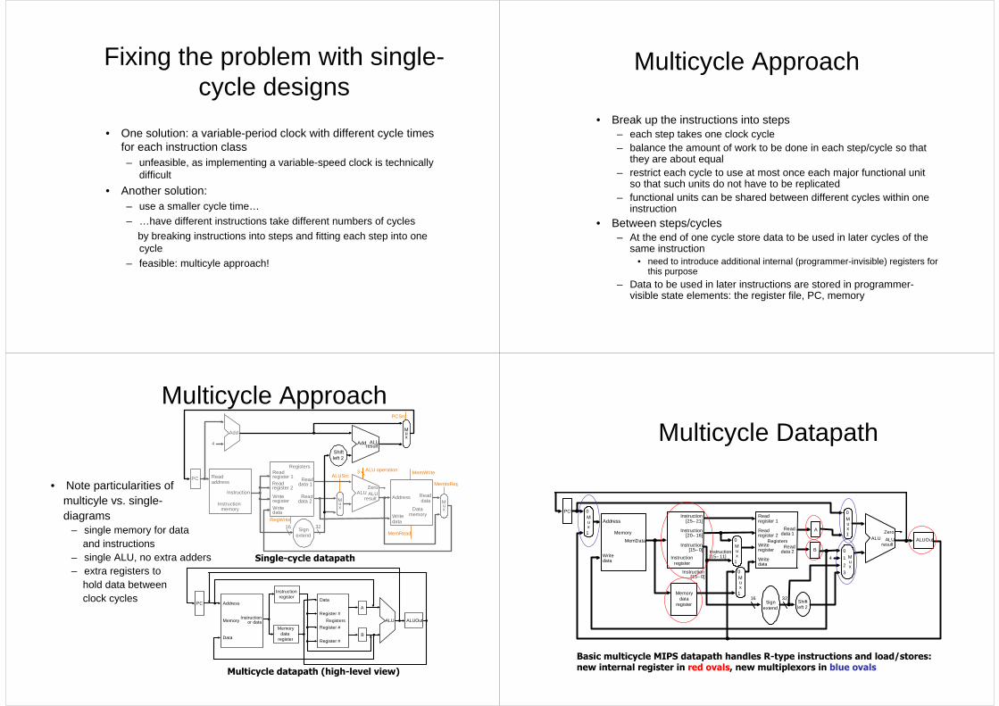
Multicycle Approach
• Note particularities ofmulticyle vs. single-diagrams
– single memory for dataand instructions
– single ALU, no extra adders– extra registers to
hold data between clock cycles
Multicycle Approach
PC
Instruction memory
Read address
Instruction
16 32
Add ALU result
M u x
Registers
Write registerWrite data
Read data 1
Read data 2
Read register 1Read register 2
Shift left 2
4
M u x
ALU operation3
RegWrite
MemRead
MemWrite
PCSrc
ALUSrc
MemtoReg
ALU result
ZeroALU
Data memory
Address
Write data
Read data M
u x
Sign extend
Add
PC
Memory
Address
Instruction or data
Data
Instruction register
Registers
Register #
Data
Register #
Register #
ALU
Memory data
register
A
B
ALUOut
Single-cycle datapath
Multicycle datapath (high-level view)
Multicycle Datapath
Shift left 2
PC
Memory
MemData
Write data
M u x
0
1
RegistersWrite register
Write data
Read data 1
Read data 2
Read register 1
Read register 2
M u x
0
1
M u x
0
1
4
Instruction [15– 0]
Sign extend
3216
Instruction [25– 21]
Instruction [20– 16]
Instruction [15– 0]
Instruction register
1 M u x
0
3
2
M u x
ALU result
ALUZero
Memory data
register
Instruction [15– 11]
A
B
ALUOut
0
1
Address
Basic multicycle MIPS datapath handles R-type instructions and load/stores:new internal register in red ovals, new multiplexors in blue ovals
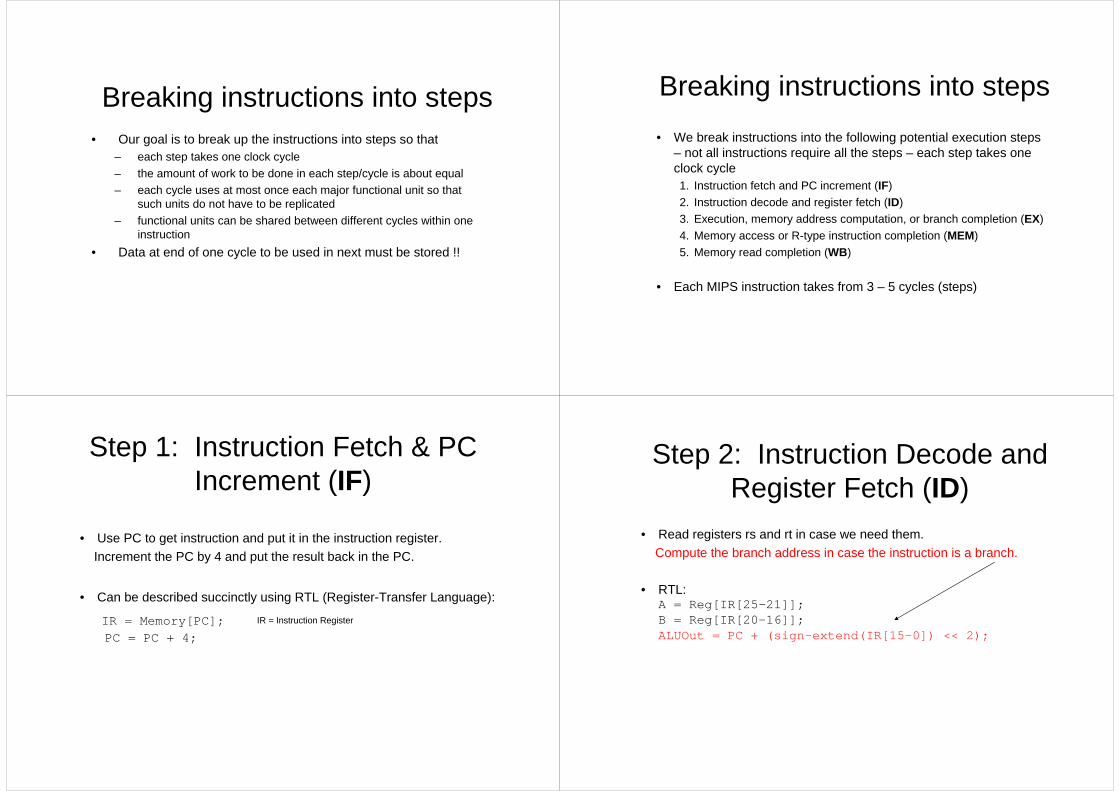
• Our goal is to break up the instructions into steps so that– each step takes one clock cycle
– the amount of work to be done in each step/cycle is about equal– each cycle uses at most once each major functional unit so that
such units do not have to be replicated
– functional units can be shared between different cycles within one instruction
• Data at end of one cycle to be used in next must be stored !!
Breaking instructions into steps Breaking instructions into steps
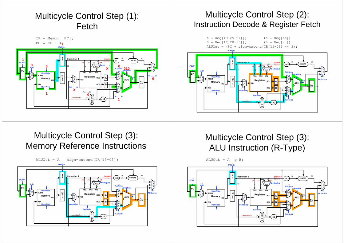
• We break instructions into the following potential execution steps – not all instructions require all the steps – each step takes one clock cycle1. Instruction fetch and PC increment (IF)
2. Instruction decode and register fetch (ID)3. Execution, memory address computation, or branch completion (EX)
4. Memory access or R-type instruction completion (MEM)
5. Memory read completion (WB)
• Each MIPS instruction takes from 3 – 5 cycles (steps)
• Use PC to get instruction and put it in the instruction register.Increment the PC by 4 and put the result back in the PC.
• Can be described succinctly using RTL (Register-Transfer Language):
IR = Memory[PC];
PC = PC + 4;
Step 1: Instruction Fetch & PC Increment (IF)
IR = Instruction Register
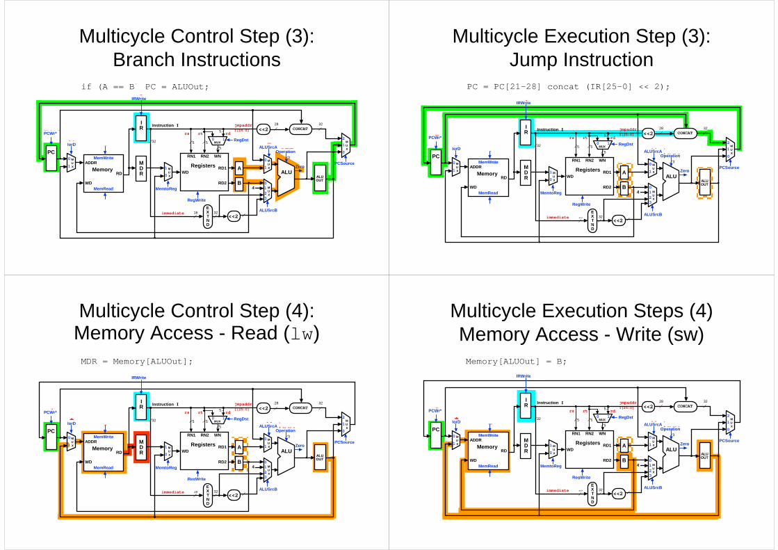
• Read registers rs and rt in case we need them.Compute the branch address in case the instruction is a branch.
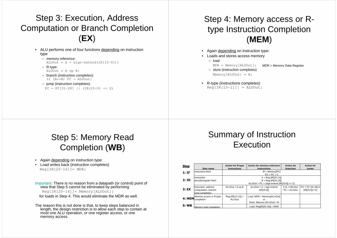
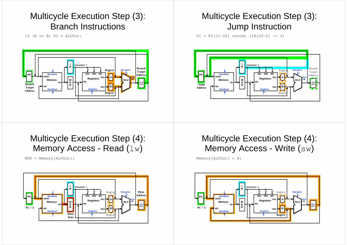
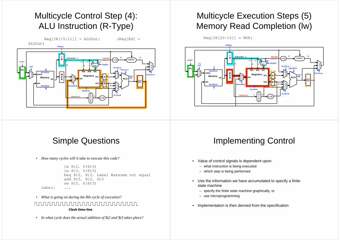
Step 4: Memory access or R-type Instruction Completion
(MEM)
MDR = Memory Data Register
• Again depending on instruction type:• Load writes back (instruction completes)
Reg[IR[20-16]]= MDR;
Important: There is no reason from a datapath (or control) point of view that Step 5 cannot be eliminated by performingReg[IR[20-16]]= Memory[ALUOut];
for loads in Step 4. This would eliminate the MDR as well.
The reason this is not done is that, to keep steps balanced in length, the design restriction is to allow each step to contain at most one ALU operation, or one register access, or one memory access.
Step 5: Memory Read Completion (WB)
Summary of Instruction Execution
Step nameAction for R-type
instructionsAction for memory-reference
instructionsAction for branches
Action for jumps
Instruction fetch IR = Memory[PC]PC = PC + 4
Instruction A = Reg [IR[25-21]]decode/register fetch B = Reg [IR[20-16]]
ALUOut = PC + (sign-extend (IR[15-0]) << 2)
Execution, address ALUOut = A op B ALUOut = A + sign-extend if (A ==B) then PC = PC [31-28] IIcomputation, branch/ (IR[15-0]) PC = ALUOut (IR[25-0]<<2)jump completion
Memory access or R-type Reg [IR[15-11]] = Load: MDR = Memory[ALUOut]completion ALUOut or
Store: Memory [ALUOut] = B
Memory read completion Load: Reg[IR[20-16]] = MDR
1: IF
2: ID
3: EX
4: MEM
5: WB
Step
Multicycle Execution Step (1):Instruction Fetch
IR = Memory[PC];PC = PC + 4;
4PC + 4
5 5
RD1
RD2
RN1 RN2 WN
WD
RegWrite
Registers
Operation
ALU
3
Zero
RD
WDMemRead
MemoryADDR
MemWrite
5
Instruction I
PC
IR
MDR
A
B
ALUOUT
IR = Instruction RegisterMDR = Memory Data Register
• What is going on during the 8th cycle of execution?
• In what cycle does the actual addition of $t2 and $t3 takes place?
Simple Questions
Clock time-line
• Value of control signals is dependent upon:– what instruction is being executed
– which step is being performed
• Use the information we have accumulated to specify a finite state machine– specify the finite state machine graphically, or
– use microprogramming
• Implementation is then derived from the specification
Implementing Control
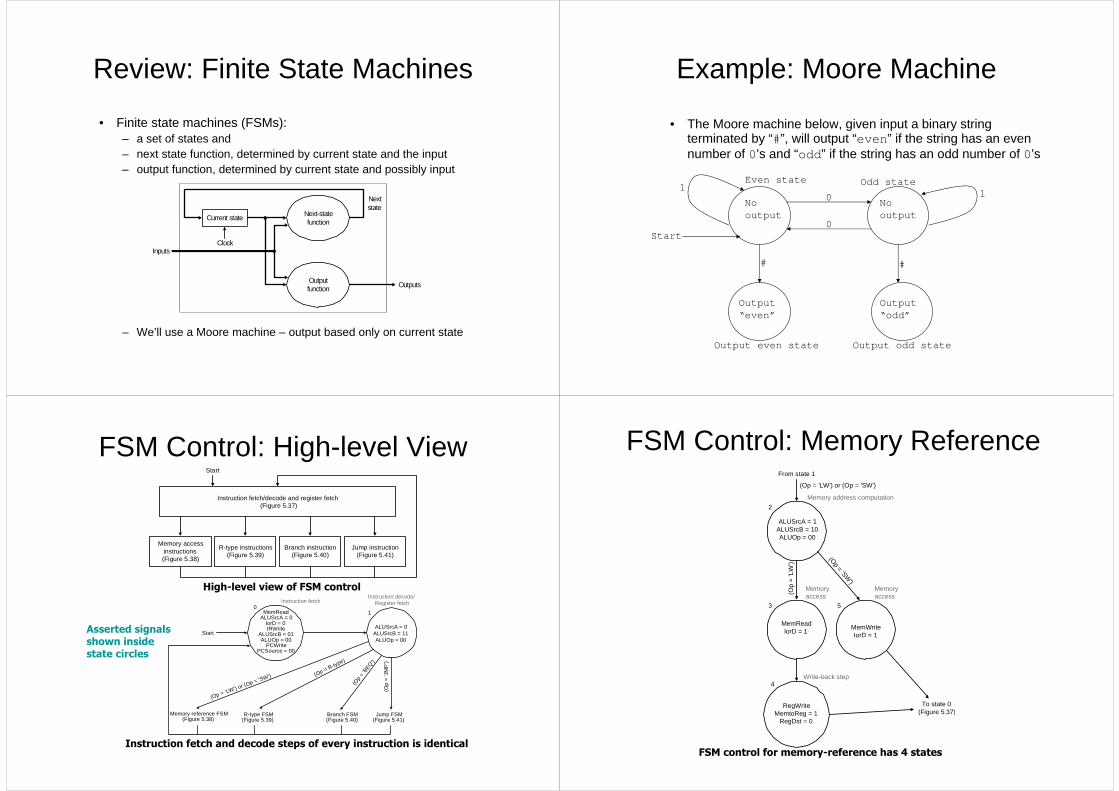
• Finite state machines (FSMs):– a set of states and – next state function, determined by current state and the input– output function, determined by current state and possibly input
– We’ll use a Moore machine – output based only on current state
Review: Finite State Machines
Next-state function
Current state
Clock
Output function
Next state
Outputs
Inputs
Example: Moore Machine
• The Moore machine below, given input a binary string terminated by “#”, will output “even ” if the string has an even number of 0’s and “odd ” if the string has an odd number of 0’s
Even state Odd state
Output even state Output odd state
Nooutput
Nooutput
Output “even”
Output “odd”
0
0
11
# #
Start
FSM Control: High-level View
Memory access instructions (Figure 5.38)
R-type instructions (Figure 5.39)
Branch instruction (Figure 5.40)
Jump instruction (Figure 5.41)
Instruction fetch/decode and register fetch (Figure 5.37)
Start
ALUSrcA = 0 ALUSrcB = 11 ALUOp = 00
MemRead ALUSrcA = 0
IorD = 0 IRWrite
ALUSrcB = 01 ALUOp = 00
PCWrite PCSource = 00
Instruction fetchInstruction decode/
Register fetch
(Op = 'LW') or (Op = 'SW') (Op = R-type)
(Op
= 'B
EQ')
(Op
= 'J
MP
')
01
Start
Memory reference FSM (Figure 5.38)
R-type FSM (Figure 5.39)
Branch FSM (Figure 5.40)
Jump FSM (Figure 5.41)
High-level view of FSM control
Instruction fetch and decode steps of every instruction is identical
Asserted signalsshown insidestate circles
FSM Control: Memory Reference
MemWrite IorD = 1
MemRead IorD = 1
ALUSrcA = 1 ALUSrcB = 10 ALUOp = 00
RegWrite MemtoReg = 1
RegDst = 0
Memory address computation
(Op = 'LW') or (Op = 'SW')
Memory access
Write-back step
(Op = 'SW
')
(Op
= 'L
W')
4
2
53
From state 1
To state 0 (Figure 5.37)
Memory access
FSM control for memory-reference has 4 states
FSM Control: R-type Instruction
ALUSrcA = 1 ALUSrcB = 00 ALUOp = 10
RegDst = 1 RegWrite
MemtoReg = 0
Execution
R-type completion
6
7
(Op = R-type)
From state 1
To state 0 (Figure 5.37)
FSM control to implement R-type instructions has 2 states
FSM Control: Branch Instruction
Branch completion
8
(Op = 'BEQ')
From state 1
To state 0 (Figure 5.37)
ALUSrcA = 1 ALUSrcB = 00 ALUOp = 01 PCWriteCond
PCSource = 01
FSM control to implement branches has 1 state
FSM Control: Jump Instruction
Jump completion
9
(Op = 'J')
From state 1
To state 0 (Figure 5.37)
PCWrite PCSource = 10
FSM control to implement jumps has 1 state
FSM Control: Complete View
PCWrite PCSource = 10
ALUSrcA = 1 ALUSrcB = 00 ALUOp = 01 PCWriteCond
PCSource = 01
ALUSrcA =1 ALUSrcB = 00 ALUOp= 10
RegDst = 1 RegWrite
MemtoReg = 0
MemWrite IorD = 1
MemRead IorD = 1
ALUSrcA = 1 ALUSrcB = 10 ALUOp = 00
RegDst =0 RegWrite
MemtoReg=1
ALUSrcA = 0 ALUSrcB = 11 ALUOp = 00
MemRead ALUSrcA = 0
IorD = 0 IRWrite
ALUSrcB = 01 ALUOp = 00
PCWrite PCSource = 00
Instruction fetchInstruction decode/
register fetch
Jump completion
Branch completionExecution
Memory address computation
Memory access
Memory access R-type completion
Write-back step
(Op = 'LW') or (Op = 'SW') (Op = R-type)
(Op
= 'B
EQ')
(Op
= 'J
')
(Op = 'SW
')
(Op
= 'L
W')
4
01
9862
753
Start
The complete FSM control for the multicycle MIPS datapath:refer Multicycle Datapath with Control II
Labels on arcs are conditionsthat determine next state
IF ID
EX
MEM
WB
Example: CPI in a multicycleCPU
• Assume– the control design of the previous slide– An instruction mix of 22% loads, 11% stores, 49% R-type operations,
16% branches, and 2% jumps• What is the CPI assuming each step requires 1 clock cycle?
• Solution:– Number of clock cycles from previous slide for each instruction class:
High-level view of FSM implementation: inputs to the combinational logic block are the current state number and instruction opcode bits; outputs are the next state number and control signals to be asserted for the current state
PCWrite
PCWriteCond
IorD
MemtoReg
PCSource
ALUOp
ALUSrcB
ALUSrcA
RegWrite
RegDst
NS3NS2NS1NS0
Op5
Op4
Op3
Op2
Op1
Op0
S3
S2
S1
S0
State register
IRWrite
MemRead
MemWrite
Instruction register opcode field
Outputs
Control logic
Inputs
Four state bits are required for 10 states
FSMControl:PLA Implem-entation
Op5
Op4
Op3
Op2
Op1
Op0
S3
S2
S1
S0
IorD
IRWrite
MemReadMemWrite
PCWritePCWriteCond
MemtoRegPCSource1
ALUOp1
ALUSrcB0ALUSrcARegWriteRegDstNS3NS2NS1NS0
ALUSrcB1ALUOp0
PCSource0
Upper half is the AND plane that computes all the products. The products are carriedto the lower OR plane by the vertical lines. The sum terms for each output is given bythe corresponding horizontal lineE.g., IorD = S0.S1.S2.S3 + S0.S1.S2.S3
• ROM (Read Only Memory)– values of memory locations are fixed ahead of time
• A ROM can be used to implement a truth table– if the address is m-bits, we can address 2m entries in the ROM– outputs are the bits of the entry the address points to
– FSM control PLA = (10x17)+(20x17) = 460 PLA cells
• PLA cells usually about the size of a ROM cell (slightly bigger)
FSM Control: ROM vs. PLA• Microprogramming is a method of specifying FSM control that
resembles a programming language – textual rather graphic– this is appropriate when the FSM becomes very large, e.g., if the
instruction set is large and/or the number of cycles per instruction is large
– in such situations graphical representation becomes difficult asthere may be thousands of states and even more arcs joining them
– a microprogram is specification : implementation is by ROM or PLA
• A microprogram is a sequence of microinstructions– each microinstruction has eight fields (label + 7 functional)
• Label: used to control microcode sequencing • ALU control: specify operation to be done by ALU• SRC1: specify source for first ALU operand• SRC2: specify source for second ALU operand• Register control: specify read/write for register file• Memory: specify read/write for memory• PCWrite control: specify the writing of the PC• Sequencing: specify choice of next microinstruction
Microprogramming
Microprogramming
• The Sequencing field value determines the execution order of the microprogram– value Seq : control passes to the sequentially next microinstruction
– value Fetch : branch to the first microinstruction to begin the next MIPS instruction, i.e., the first microinstruction in the microprogram
– value Dispatch i : branch to a microinstruction based on control input and a dispatch table entry (called dispatching):
• Dispatching is implemented by means of creating a table, called dispatch table, whose entries are microinstruction labels and which is indexed by the control input. There may be multiple dispatch tables –the value Dispatch i in the sequencing field indicates that the i thdispatch table is to be used
Control Microprogram
• The microprogram corresponding to the FSM control shown graphically earlier:
LabelALU
control SRC1 SRC2Register control Mem ory
PCW rite control Sequencing
Fetch Add PC 4 Read PC ALU SeqAdd PC Extshft Read Dispatch 1
M em1 Add A Extend Dispatch 2LW 2 Read ALU Seq
W rite MDR FetchSW 2 W rite ALU FetchRform at1 Func code A B Seq
W rite ALU FetchBEQ1 Subt A B ALUOut-cond FetchJUM P1 Jump address Fetch
– typically manufacturer designs architecture and microcode in parallel
• Implementation advantages
– easy to change since values are in memory (e.g., off-chip ROM)
– can emulate other architectures
– can make use of internal registers
• Implementation disadvantages
– control is implemented nowadays on same chip as processor so the
advantage of an off-chip ROM does not exist
– ROM is no longer faster than on-board cache
– there is little need to change the microcode as general-purpose
computers are used far more nowadays than computers designed for
specific applications
Summary
• Techniques described in this chapter to design datapaths and control are at the core of all modern computer architecture
• Multicycle datapaths offer two great advantages over single-cycle– functional units can be reused within a single instruction if they are
accessed in different cycles – reducing the need to replicate expensive logic
– instructions with shorter execution paths can complete quicker by consuming fewer cycles
• Modern computers, in fact, take the multicycle paradigm to a higher level to achieve greater instruction throughput: – pipelining (next topic) where multiple instructions execute
simultaneously by having cycles of different instructions overlap in the datapath
– the MIPS architecture was designed to be pipelined