In recent years, the trend within the molded optics community has been an overall advancement in the capability to diamond grind molds using a variety of grinding techniques. Improvements in grinding equipment, materials and tooling have enabled higher quality ceramic and carbide molds and thereby lenses. Diamond turned molds from ductile metals are still used prevalently throughout the molding industry. Each technology presents a unique set of advantages and disadvantages whether used for precision injection molding of plastic optics or precision glass molding. This paper reviews the manufacturing techniques for each approach and applicable molding process. The advantages and disadvantages of each are compared and analyzed. The subtle differences that exist in optics molded from each technique and the impact they have on the performance in various applications is reviewed. Differences stemming from tooling material properties, material-specific minor defects, as well as cutting and grinding process-induced artifacts are described in detail as well as their influence on the roughness, waviness, and form errors present on the molded surface. A comparison with results between similar surfaces for both diamond grinding and diamond turning is presented. Keywords: Precision glass molding, Plastic optics, molding, diamond grinding, diamond turning, power spectral density.
1. INTRODUCTION Molds for precision injection molding of plastic optics or for precision glass molding (PGM) are manufactured using either precision diamond turning or precision diamond grinding to generate the optical surface. The molds are a critical piece of the individual molding processes. The molded component replicates the surface of the mold, any defects on the molds will be replicated on the component itself, and therefore in order to have a good understanding of the defects associated with a particular molding process it is imperative to have a good understanding of the mold manufacturing process. The individual processes themselves are well documented and there are several good references on the manufacture of polymer opticsi,ii PGMiii, and even comparisons of the twoiv, the scope of which is beyond this paper.
The molds for manufacturing plastic optics are generally single point diamond turned (SPDT). Precision ground carbide molds could be also be used, however the additional expense is usually not warranted. These SPDT molds require a material that can be readily cut and are typically electroless phosphor nickel plated steel molds (Nickel Molds).
Carbide or ceramic tooling is required in PGM because of the high temperatures required during processing. The electro-less phosphor nickel will break down at typical PGM temperatures. However for some glasses with very low glass transition temperatures, Tg, nickel molds have historically been used. These very low Tg glass types, such as Corning CO-550, typically had high lead contents (CO-550 was ≈30% PbO). These glass types are no longer used in the industry due to environmental restrictions except in rare circumstances. There are a limited number of very low Tg, (Tg< 400°C), still available for PGM that do not contain lead, such as ECO550v. Therefore for the majority of circumstances it is safe to make the following generalization:
End Product Mold Type Mold Manufacturing Process
Injection Mold Plastic Optics Nickel Molds Single Point Diamond Turning
A general overview of each of the mold manufacturing processes follows in Sections 1.1 and 1.2. Section 2 reviews the material characteristics of the individual mold types and also evaluates the potential mold defects that are material dependent. Section 3 reviews the impact of the individual mold cutting processes and techniques on the quality of the molds. Section 4 then provides an empirical evaluation of two different PGM lenses manufactured using the two independent manufacturing chains. Finally a comparison of the results is discussed and conclusions are drawn in Section 5.
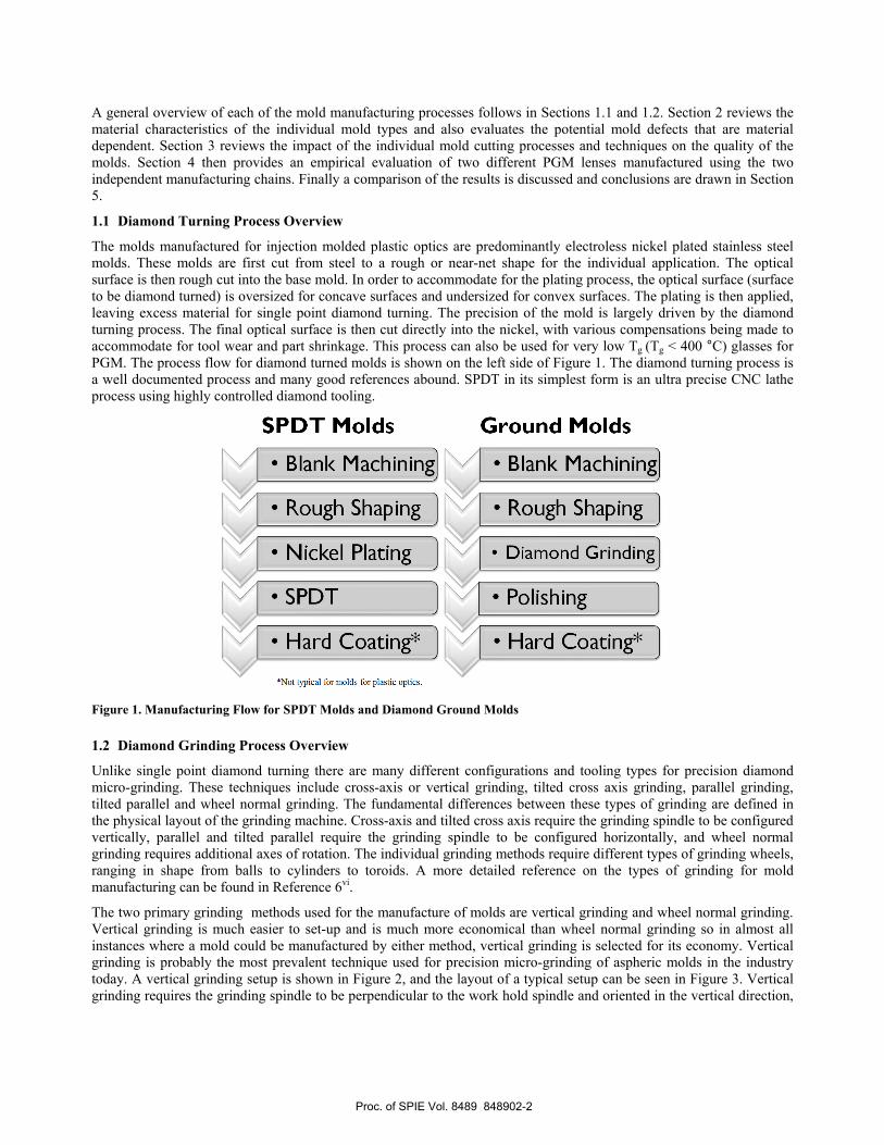
1.1 Diamond Turning Process Overview
The molds manufactured for injection molded plastic optics are predominantly electroless nickel plated stainless steel molds. These molds are first cut from steel to a rough or near-net shape for the individual application. The optical surface is then rough cut into the base mold. In order to accommodate for the plating process, the optical surface (surface to be diamond turned) is oversized for concave surfaces and undersized for convex surfaces. The plating is then applied, leaving excess material for single point diamond turning. The precision of the mold is largely driven by the diamond turning process. The final optical surface is then cut directly into the nickel, with various compensations being made to accommodate for tool wear and part shrinkage. This process can also be used for very low Tg (Tg < 400 °C) glasses for PGM. The process flow for diamond turned molds is shown on the left side of Figure 1. The diamond turning process is a well documented process and many good references abound. SPDT in its simplest form is an ultra precise CNC lathe process using highly controlled diamond tooling.
Figure 1. Manufacturing Flow for SPDT Molds and Diamond Ground Molds 1.2 Diamond Grinding Process Overview
Unlike single point diamond turning there are many different configurations and tooling types for precision diamond micro-grinding. These techniques include cross-axis or vertical grinding, tilted cross axis grinding, parallel grinding, tilted parallel and wheel normal grinding. The fundamental differences between these types of grinding are defined in the physical layout of the grinding machine. Cross-axis and tilted cross axis require the grinding spindle to be configured vertically, parallel and tilted parallel require the grinding spindle to be configured horizontally, and wheel normal grinding requires additional axes of rotation. The individual grinding methods require different types of grinding wheels, ranging in shape from balls to cylinders to toroids. A more detailed reference on the types of grinding for mold manufacturing can be found in Reference 6vi.
The two primary grinding methods used for the manufacture of molds are vertical grinding and wheel normal grinding. Vertical grinding is much easier to set-up and is much more economical than wheel normal grinding so in almost all instances where a mold could be manufactured by either method, vertical grinding is selected for its economy. Vertical grinding is probably the most prevalent technique used for precision micro-grinding of aspheric molds in the industry today. A vertical grinding setup is shown in Figure 2, and the layout of a typical setup can be seen in Figure 3. Vertical grinding requires the grinding spindle to be perpendicular to the work hold spindle and oriented in the vertical direction,
Proc. of SPIE Vol. 8489 848902-2
r° ^.,r,.+
.m'r..+
IN' lisa.) b.) c.)
hence the name. The radius of the wheel is used to compensate the cutter path for the mold prescription. Grinding is not nearly as deterministic as SPDT due to the less predictable wear of the grinding wheel. The grinding wheel traverses the pre-programmed tool path removing small amounts of material with each pass, similar to the SPDT process. The wheel starts at the outside edge and moves towards the central region of the mold. Vertical grinding can not be used for certain mold geometries due to restrictions on the grinding wheel shaft diameter and limitations on the size of the wheel itself As can be seen in Figure 3b, if the mold cavity was excessively deep, the shaft of the grinding wheel could interfere with the mold and prevent manufacture. Figure 3c shows the horizontal cutaway of the vertical grinding process. If the diameter of the mold is too small the tool may not be able to fit within the cavity.
Figure 2. Vertical Diamond Grinding
Figure 3. Vertical Grinding of 354996 Mold, a.) Isometric View b.) Vertical Cross Section and c.) Horizontal
Cross Section.
2. MATERIAL CHARACTERISTICS AND POTENTIAL DEFECTS By far, the most common mold materials used to shape optics in industry today are electroless nickel and tungsten carbide. While each of these materials has advantages and disadvantages when considering their use in various applications, in general electroless nickel has been used primarily for plastics and very-low-Tg glasses. Alternately, tungsten carbide is often the choice material in the molding of high-temperature glasses. It can be used for molding simple aspheric, spherical, and plano optical surfaces, and is especially advantageous for low-cost, high volume manufacturing.
Proc. of SPIE Vol. 8489 848902-3
The driving reasons for these preferences stem from fundamental material properties and the consequent fabrication, process, and cost constraints they impose. Additionally, each of these materials is susceptible to its own unique material-related defects that can be exhibited in the finished molded optic. For this reason it is useful to be familiar with these potential flaws and to specify the desired optic appropriately so fabricators can either limit or eliminate features that may have a negative impact on the optical performance in any particular application.
2.1 Electroless Nickel
Electroless nickel (EN) plating has been commercially available since the mid-1950’s, and its’ chemical and material properties are well understood.vii The prevalence of diamond-turned electroless nickel in molding plastics and low-Tg glasses is primarily due to its favorable machinability and relative stability at low molding temperatures. These characteristics can be traced to the material’s good ductility and amorphous grain structure.
However, at high temperatures these properties begin to break down with the formation of crystalline-phase grains within the platingviii. In essence, the non-equilibrium solid mixture of nickel and (typically) 11-13% phosphorus yields rapidly to equilibrium phases, driven by the high temperature conditions. This transformation is particularly rapid at temperatures higher than 400°C.
In practice, molding temperatures are higher than the glass transition temperature, and lenses molded from some low-Tg glasses can still be affected by this phenomenon. The effect produces an overall volumetric contraction of the mold’s nickel plating and exhibits itself on the mold (often slowly over time, depending on the maximum process temperature) as a milky haze uniformly distributed over the molding surface. Under high magnification, the surface can appear distorted and often acquires a fine orange-peel-like texture, thus driving up roughness and high-frequency waviness errors, which consequently get replicated onto the molded optic. High and mid-spatial frequencies such as these can cause excessive scatter loss and/or behave like a miniature grating, leading to diffraction effects.ix
Nickel phase transformation can also lead to progressive form disfigurement during processing if the underlying substrate which supports the plating has excessive form error. This condition causes the nickel thickness to vary over the optic-forming surface after diamond turning. Consequently, even nearly-perfect molds after turning will distort when the nickel shrinks during processing, producing a varying surface displacement across the optic-forming aperture. The effect also causes the base radius of concave mold cavities to grow slightly, and convex ones to contract. In addition, any EN mold surfaces that are used to constrain optical surface alignment in the molded component are subject to change during shrinkage, possibly affecting coma aberration in the finished optic. These phenomena are well understood and compensated for by competent PGM fabricators. However, for molded optics with exceedingly tight optical performance specifications, or when the maximum glass processing temperature is sufficiently high, it may be more advantageous to opt for ceramic or tungsten carbide tooling, which is far more stable at high temperatures.
One method sometimes used to stabilize electroless nickel is the heat treatment (>400°C) of molds prior to turning. Unfortunately, this offers only limited advantage, as the crystalline formation also causes a dramatic increase in diamond tool wear, which then restricts the finest achievable surface finish of the turned mold. This obviously worsens when as mold size (optic size) becomes large, due to the increase in effective cutting length needed to continuously machine the entire molding surface. However, since the material has been pre-shrunk to nearly compositional phase equilibrium, the practice will produce a more-stable and repeatable replication of the optics throughout the molding process, although bought at a significant cost. This option is usually only employed for smaller optics (< 5mm aperture) and when production volumes are relatively low.
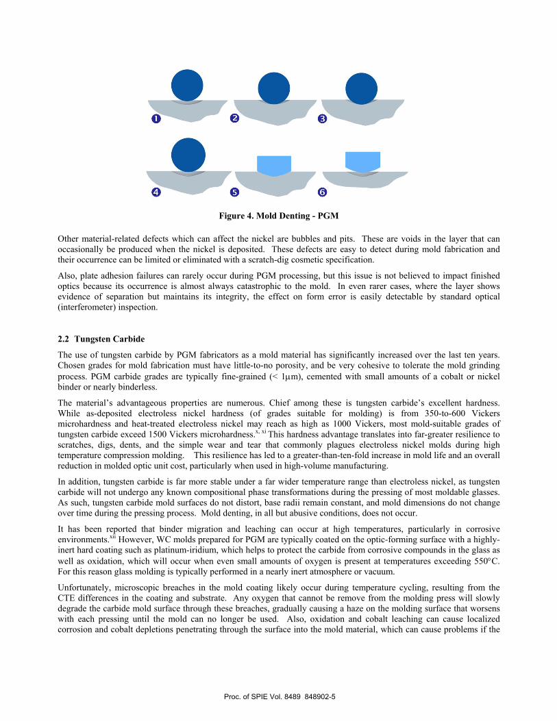
A more common defect that can affect nickel molds during the pressing process is mold denting. This can occur if the glass is not heated high enough or long enough to thoroughly soften the glass. Long-radius mold surfaces pressing small-radius glass preforms are most susceptible, since the initial contact area of the mold and glass is very small, driving the contact pressure during pressing to extremes. During processing, the resulting defect replicated on the molded optic usually starts as a barely-detectable mid-spatial-frequency wave in the optic’s center, detected during routine interferometer inspection. This feature progressively worsens with each subsequent lens pressing until the replicated dent feature exceeds optical performance specifications. For some glasses and mold geometries, using a high-enough softening temperature causes other unrelated, but more-detrimental effects on the molded optic. For these cases it is advisable to use hard tooling, such as tungsten carbide.
Proc. of SPIE Vol. 8489 848902-4
Air sirmilirwar -Trare _ 0
Figure 4. Mold Denting - PGM
Other material-related defects which can affect the nickel are bubbles and pits. These are voids in the layer that can occasionally be produced when the nickel is deposited. These defects are easy to detect during mold fabrication and their occurrence can be limited or eliminated with a scratch-dig cosmetic specification.
Also, plate adhesion failures can rarely occur during PGM processing, but this issue is not believed to impact finished optics because its occurrence is almost always catastrophic to the mold. In even rarer cases, where the layer shows evidence of separation but maintains its integrity, the effect on form error is easily detectable by standard optical (interferometer) inspection.
2.2 Tungsten Carbide
The use of tungsten carbide by PGM fabricators as a mold material has significantly increased over the last ten years. Chosen grades for mold fabrication must have little-to-no porosity, and be very cohesive to tolerate the mold grinding process. PGM carbide grades are typically fine-grained (< 1μm), cemented with small amounts of a cobalt or nickel binder or nearly binderless.
The material’s advantageous properties are numerous. Chief among these is tungsten carbide’s excellent hardness. While as-deposited electroless nickel hardness (of grades suitable for molding) is from 350-to-600 Vickers microhardness and heat-treated electroless nickel may reach as high as 1000 Vickers, most mold-suitable grades of tungsten carbide exceed 1500 Vickers microhardness.x, xi This hardness advantage translates into far-greater resilience to scratches, digs, dents, and the simple wear and tear that commonly plagues electroless nickel molds during high temperature compression molding. This resilience has led to a greater-than-ten-fold increase in mold life and an overall reduction in molded optic unit cost, particularly when used in high-volume manufacturing.
In addition, tungsten carbide is far more stable under a far wider temperature range than electroless nickel, as tungsten carbide will not undergo any known compositional phase transformations during the pressing of most moldable glasses. As such, tungsten carbide mold surfaces do not distort, base radii remain constant, and mold dimensions do not change over time during the pressing process. Mold denting, in all but abusive conditions, does not occur.
It has been reported that binder migration and leaching can occur at high temperatures, particularly in corrosive environments.xii However, WC molds prepared for PGM are typically coated on the optic-forming surface with a highly-inert hard coating such as platinum-iridium, which helps to protect the carbide from corrosive compounds in the glass as well as oxidation, which will occur when even small amounts of oxygen is present at temperatures exceeding 550°C. For this reason glass molding is typically performed in a nearly inert atmosphere or vacuum.
Unfortunately, microscopic breaches in the mold coating likely occur during temperature cycling, resulting from the CTE differences in the coating and substrate. Any oxygen that cannot be remove from the molding press will slowly degrade the carbide mold surface through these breaches, gradually causing a haze on the molding surface that worsens with each pressing until the mold can no longer be used. Also, oxidation and cobalt leaching can cause localized corrosion and cobalt depletions penetrating through the surface into the mold material, which can cause problems if the
Proc. of SPIE Vol. 8489 848902-5
mold is intended to be re-surfaced and re-coated for continued use. These localized degradations become apparent on a re-surfaced mold as well-defined rough patches on the tungsten carbide surface. Molds in this condition are usually discarded. Obviously, for these reasons, the use of acids to clean mold surfaces are to be avoided.
Oxidation of alignment surfaces can also occur, which must be periodically cleaned, as oxides can flake away and contaminate the molded optic, resulting in cosmetic failure loss in PGM processing. Mold material loss through oxidation and cleaning will over time destroy the dimensional accuracy of the alignment surfaces and eventually render the mold pin unusable. However, in well-controlled press atmospheres, this does not become problematic until the total mold pin life exceeds tens of thousands of cycles.
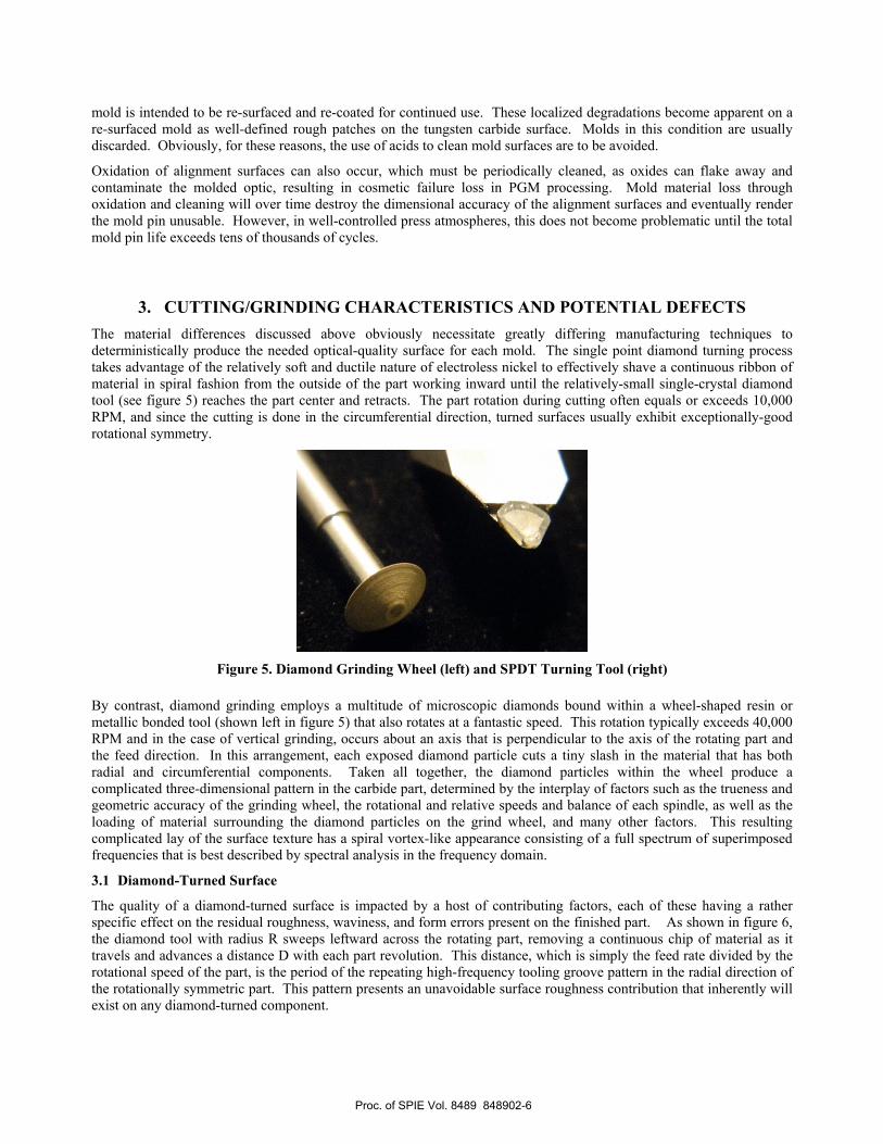
3. CUTTING/GRINDING CHARACTERISTICS AND POTENTIAL DEFECTS The material differences discussed above obviously necessitate greatly differing manufacturing techniques to deterministically produce the needed optical-quality surface for each mold. The single point diamond turning process takes advantage of the relatively soft and ductile nature of electroless nickel to effectively shave a continuous ribbon of material in spiral fashion from the outside of the part working inward until the relatively-small single-crystal diamond tool (see figure 5) reaches the part center and retracts. The part rotation during cutting often equals or exceeds 10,000 RPM, and since the cutting is done in the circumferential direction, turned surfaces usually exhibit exceptionally-good rotational symmetry.
By contrast, diamond grinding employs a multitude of microscopic diamonds bound within a wheel-shaped resin or metallic bonded tool (shown left in figure 5) that also rotates at a fantastic speed. This rotation typically exceeds 40,000 RPM and in the case of vertical grinding, occurs about an axis that is perpendicular to the axis of the rotating part and the feed direction. In this arrangement, each exposed diamond particle cuts a tiny slash in the material that has both radial and circumferential components. Taken all together, the diamond particles within the wheel produce a complicated three-dimensional pattern in the carbide part, determined by the interplay of factors such as the trueness and geometric accuracy of the grinding wheel, the rotational and relative speeds and balance of each spindle, as well as the loading of material surrounding the diamond particles on the grind wheel, and many other factors. This resulting complicated lay of the surface texture has a spiral vortex-like appearance consisting of a full spectrum of superimposed frequencies that is best described by spectral analysis in the frequency domain.
3.1 Diamond-Turned Surface
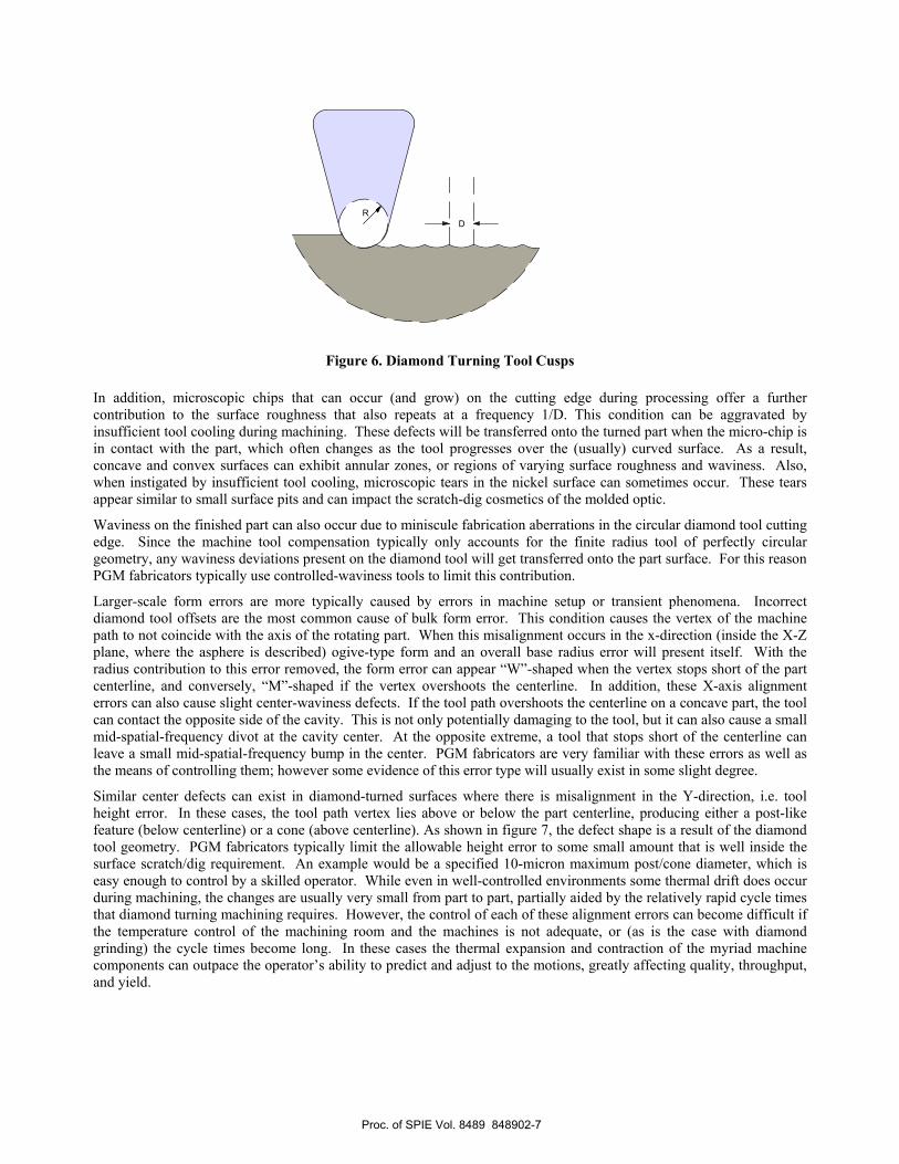
The quality of a diamond-turned surface is impacted by a host of contributing factors, each of these having a rather specific effect on the residual roughness, waviness, and form errors present on the finished part. As shown in figure 6, the diamond tool with radius R sweeps leftward across the rotating part, removing a continuous chip of material as it travels and advances a distance D with each part revolution. This distance, which is simply the feed rate divided by the rotational speed of the part, is the period of the repeating high-frequency tooling groove pattern in the radial direction of the rotationally symmetric part. This pattern presents an unavoidable surface roughness contribution that inherently will exist on any diamond-turned component.
Proc. of SPIE Vol. 8489 848902-6
Figure 6. Diamond Turning Tool Cusps
In addition, microscopic chips that can occur (and grow) on the cutting edge during processing offer a further contribution to the surface roughness that also repeats at a frequency 1/D. This condition can be aggravated by insufficient tool cooling during machining. These defects will be transferred onto the turned part when the micro-chip is in contact with the part, which often changes as the tool progresses over the (usually) curved surface. As a result, concave and convex surfaces can exhibit annular zones, or regions of varying surface roughness and waviness. Also, when instigated by insufficient tool cooling, microscopic tears in the nickel surface can sometimes occur. These tears appear similar to small surface pits and can impact the scratch-dig cosmetics of the molded optic.
Waviness on the finished part can also occur due to miniscule fabrication aberrations in the circular diamond tool cutting edge. Since the machine tool compensation typically only accounts for the finite radius tool of perfectly circular geometry, any waviness deviations present on the diamond tool will get transferred onto the part surface. For this reason PGM fabricators typically use controlled-waviness tools to limit this contribution.
Larger-scale form errors are more typically caused by errors in machine setup or transient phenomena. Incorrect diamond tool offsets are the most common cause of bulk form error. This condition causes the vertex of the machine path to not coincide with the axis of the rotating part. When this misalignment occurs in the x-direction (inside the X-Z plane, where the asphere is described) ogive-type form and an overall base radius error will present itself. With the radius contribution to this error removed, the form error can appear “W”-shaped when the vertex stops short of the part centerline, and conversely, “M”-shaped if the vertex overshoots the centerline. In addition, these X-axis alignment errors can also cause slight center-waviness defects. If the tool path overshoots the centerline on a concave part, the tool can contact the opposite side of the cavity. This is not only potentially damaging to the tool, but it can also cause a small mid-spatial-frequency divot at the cavity center. At the opposite extreme, a tool that stops short of the centerline can leave a small mid-spatial-frequency bump in the center. PGM fabricators are very familiar with these errors as well as the means of controlling them; however some evidence of this error type will usually exist in some slight degree.
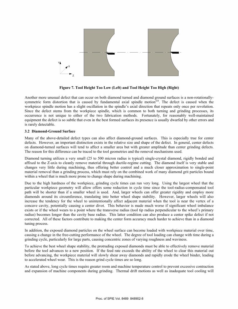
Similar center defects can exist in diamond-turned surfaces where there is misalignment in the Y-direction, i.e. tool height error. In these cases, the tool path vertex lies above or below the part centerline, producing either a post-like feature (below centerline) or a cone (above centerline). As shown in figure 7, the defect shape is a result of the diamond tool geometry. PGM fabricators typically limit the allowable height error to some small amount that is well inside the surface scratch/dig requirement. An example would be a specified 10-micron maximum post/cone diameter, which is easy enough to control by a skilled operator. While even in well-controlled environments some thermal drift does occur during machining, the changes are usually very small from part to part, partially aided by the relatively rapid cycle times that diamond turning machining requires. However, the control of each of these alignment errors can become difficult if the temperature control of the machining room and the machines is not adequate, or (as is the case with diamond grinding) the cycle times become long. In these cases the thermal expansion and contraction of the myriad machine components can outpace the operator’s ability to predict and adjust to the motions, greatly affecting quality, throughput, and yield.
RD
Proc. of SPIE Vol. 8489 848902-7
Y
Z
X
Figure 7. Tool Height Too Low (Left) and Tool Height Too High (Right) Another more unusual defect that can occur on both diamond turned and diamond ground surfaces is a non-rotationally-symmetric form distortion that is caused by fundamental axial spindle motionxiii. The defect is caused when the workpiece spindle motion has a slight oscillation in the spindle’s axial direction that repeats only once per revolution. Since the defect stems from the workpiece spindle, which is common to both turning and grinding processes, its occurrence is not unique to either of the two fabrication methods. Fortunately, for reasonably well-maintained equipment the defect is so subtle that even in the best formed surfaces its presence is usually dwarfed by other errors and is rarely detectable.
3.2 Diamond-Ground Surface
Many of the above-detailed defect types can also affect diamond-ground surfaces. This is especially true for center defects. However, an important distinction exists in the relative size and shape of the defect. In general, center defects on diamond-turned surfaces will tend to affect a smaller area but with greater amplitude than center grinding defects. The reason for this difference can be traced to the tool geometries and the removal mechanisms used.
Diamond turning utilizes a very small (25 to 500 micron radius is typical) single-crystal diamond, rigidly bonded and affixed to the Z-axis to cleanly remove material through ductile-regime cutting. The diamond itself is very stable and changes very little during machining, thus offering better control and a much closer approximation to single-point material removal than a grinding process, which must rely on the combined work of many diamond grit particles bound within a wheel that is much more prone to change shape during machining.
Due to the high hardness of the workpiece, grinding cycle times can run very long. Using the largest wheel that the particular workpiece geometry will allow offers some reduction in cycle time since the tool-radius-compensated tool path will be shorter than if a smaller wheel is used. And, larger wheels can offer greater rigidity and employ more diamonds around its circumference, translating into better wheel shape stability. However, larger wheels will also increase the tendency for the wheel to unintentionally affect adjacent material when the tool is near the vertex of a concave cavity, potentially causing a center divot. This behavior is made much worse if significant wheel imbalance exists or if the wheel wears to a point where the transverse radius (tool tip radius perpendicular to the wheel’s primary radius) becomes longer than the cavity base radius. This latter condition can also produce a center spike defect if not corrected. All of these factors contribute to making the center form accuracy much harder to achieve than in a diamond tuning process.
In addition, the exposed diamond particles on the wheel surface can become loaded with workpiece material over time, causing a change in the free-cutting performance of the wheel. The degree of tool loading can change with time during a grinding cycle, particularly for large parts, causing concentric zones of varying roughness and waviness.
To achieve the best wheel shape stability, the protruding exposed diamonds must be able to effectively remove material before the tool advances to a new position. If the feed rate exceeds the ability of the wheel to clear this material out before advancing, the workpiece material will slowly shear away diamonds and rapidly erode the wheel binder, leading to accelerated wheel wear. This is the reason grind cycle times are so long.
As stated above, long cycle times require greater room and machine temperature control to prevent excessive contraction and expansion of machine components during grinding. Thermal drift motions as well as inadequate tool cooling will
Proc. of SPIE Vol. 8489 848902-8
cause a host of problems that are vastly more detrimental than in diamond turning processes. The reasons for this are largely due to the longer machine cycle times, the greater elasticity of the grind tool/spindle system, shallower optimal cut depths, and the propensity for tool shape deformation, all of which can lead to excessive form, waviness, and roughness errors.
Another condition that can strongly affect the occurrence of mid-spatial-frequency errors is workpiece/grind spindle resonant frequencies. When a repeating integer number of grind spindle vibrations occur with each rotation of the workpiece, a pattern begins to build across the ground part that can range in appearance from a slight spiral to fully radial spokes, depending on how well-tuned the resonance is. Even an exceptionally well-balanced spindle can produce this effect. Fortunately the condition can easily be remedied by slightly altering the speed of either spindle.
4. SURFACE TOPOLOGY DIFFERENCES In order to quantify the assertions of sections 2 and 3, two lenses with fundamentally different manufacturing process are evaluated. The lenses used to compare the mold manufacturing techniques are LightPath Technologies Inc., part numbers 350996 and 354996. LightPath’s lens part numbering system uses the first three digits to identify the glass type and the second three as a unique identifier. “350” indicates the glass used is Corning CO-550, a very-low Tg glass and “354” identifies CDGM’s D-ZK3 a low Tg glass, but much higher than CO-550. Table 1 compares the glass properties of each:
Table 1. Glass Comparison CO-550 versus D-ZK3xiv.xv
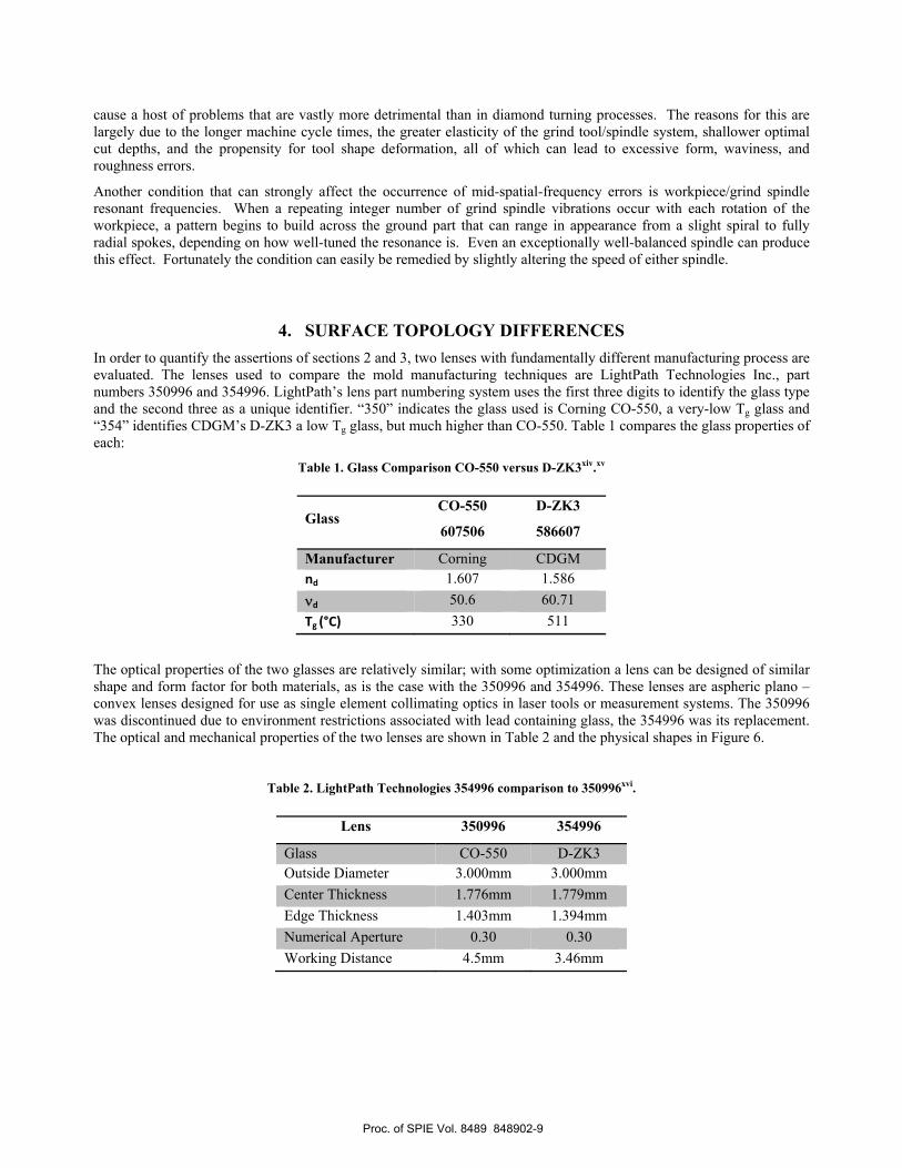
The optical properties of the two glasses are relatively similar; with some optimization a lens can be designed of similar shape and form factor for both materials, as is the case with the 350996 and 354996. These lenses are aspheric plano – convex lenses designed for use as single element collimating optics in laser tools or measurement systems. The 350996 was discontinued due to environment restrictions associated with lead containing glass, the 354996 was its replacement. The optical and mechanical properties of the two lenses are shown in Table 2 and the physical shapes in Figure 6.
Table 2. LightPath Technologies 354996 comparison to 350996xvi.
Figure 6. Physical Comparison of 350996 and 354996
4.1 Using the Power-Spectral Density to Characterize a Surface
Diamond turning and grinding surface finishing processes have enabled a myriad of new optical surface geometries that were once not possible to produce using conventional glass grinding and polishing techniques. However, these new deterministic-finishing processes have also led to a greater variety of topographic features that can be formed on the optic (such as those detailed in section 3), in contrast to the more-randomized texture inherent to conventionally ground and polished lenses.
Deterministic finishing techniques have also enabled the mass production of optical elements using PGM, and as a result have forced both fabricators and end users to become more attentive to not only the usual bulk optical-surface quality indicators, such as peak-to-valley and root-mean-squared errors, but also to the magnitude and proportion of errors within specific spatial frequency bands. These application-dependent spatial frequency sensitivities, typically due to scattering effects from roughness and mid-spatial frequency irregularities, are becoming better understood.
Highly instrumental toward the measurement of specific spatial frequency band errors has been the application of the Fourier transform to provide the power spectral density (PSD) of any given surfacexvii,xviii,xix,xx,xxi,xxii. In this technique, raw spatial data, typically gathered by interferometer or profilometer, is transformed through the Fourier algorithm to produce a plot of power density vs. spatial frequency. In 1988, Church first showed that PSD plots of conventionally-figured and polished isotropic materials will theoretically form a nearly straight line when plotted on a log-log graph, revealing an adherence to the inverse power lawxxiii. In essence the surface is expected to be scale-symmetric, exhibiting fractal-like behavior. However, an overabundance or dearth of any particular frequency, which is common to deterministically-finished surfaces, will exhibit a corresponding spike or dip in the PSD plot at that frequency.
Moreover, by employing Parseval’s theorem, it can be demonstrated that the square root of the area under the PSD curve is proportional to the RMS calculated in the spatial domain.xix This relationship forms the basis by which the 350996 and 354996 mold surfaces will be characterized and compared. In essence, the full frequency domain of the PSD of each mold sample is broken into three sub-domains, one each for form, waviness, and roughness. For each of these frequency bands the proportion of the frequency band RMS to the total RMS error is calculated through the area under the PSD curve. These proportions are then factored into the RMS calculated in the spatial domain to reflect the individual frequency band contribution to the overall RMS, reported in terms fully consistent with the more-traditional bulk RMS metric. In this way the root mean squared error specification can be thought of as a budget, where the sum of the individual frequency band RMS errors equal the total bulk error RMS.
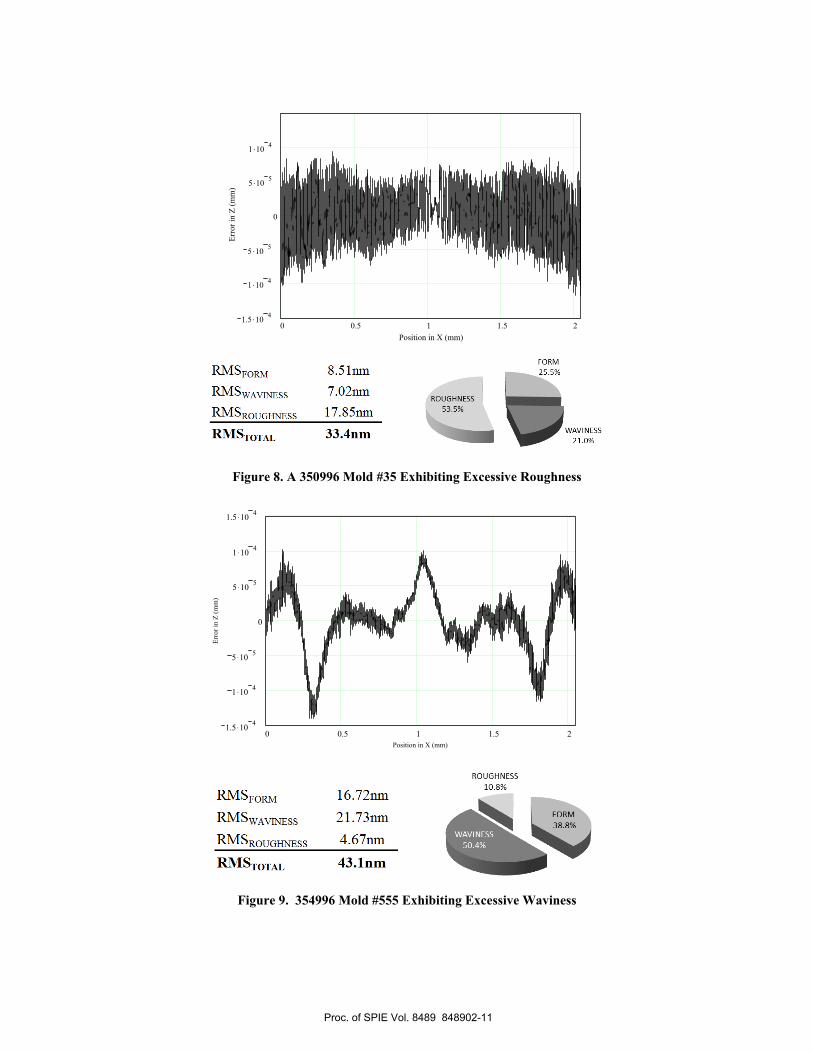
The utility of this approach is well illustrated in the surface form profiles shown in figures 8, 9, and 10. While each of the three X996 mold bulk RMS irregularity values are similar to one another and are well below the specified limit of 105.5 nm, only the mold in figure 10 had sufficiently low waviness and roughness to meet the requirements of the application.
Proc. of SPIE Vol. 8489 848902-10
RMSFORM
RMSWAVINESS
RMSROUGIINESS
RMSTOTAE
8.51nm
7.02nm
17.85nm
33.4nm
FORM
WAVINESS
21.0%
RMSFORM
RIVISwAVINESS
RMSROUGHNESS
RMSTOTAL
16.72nm
21.73nm
4.67nm
43.1nm
ROUGHNESS
10.8%
0 0.5 1 1.5 21.5 .10 4
1 .10 4
5 .10 5
0
5 .10 5
1 .10 4
Position in X (mm)
Erro
r in
Z (m
m)
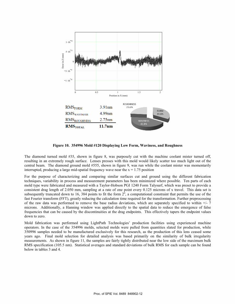
Figure 8. A 350996 Mold #35 Exhibiting Excessive Roughness
The diamond turned mold #35, shown in figure 8, was purposely cut with the machine coolant mister turned off, resulting in an extremely rough surface. Lenses presses with this mold would likely scatter too much light out of the central beam. The diamond ground mold #555, shown in figure 9, was run while the coolant mister was momentarily interrupted, producing a large mid-spatial frequency wave near the x = 1.75 position
For the purpose of characterizing and comparing similar surfaces cut and ground using the different fabrication techniques, variability in process and measurement parameters has been minimized where possible. Ten parts of each mold type were fabricated and measured with a Taylor-Hobson PGI 1240 Form Talysurf, which was preset to provide a consistent drag length of 2.050 mm, sampling at a rate of one point every 0.125 microns of x travel. This data set is subsequently truncated down to 16, 384 points to fit the form 2n, a computational constraint that permits the use of the fast Fourier transform (FFT), greatly reducing the calculation time required for the transformation. Further preprocessing of the raw data was performed to remove the base radius deviations, which are separately specified to within +/- 7 microns. Additionally, a Hanning window was applied directly to the spatial data to reduce the emergence of false frequencies that can be caused by the discontinuities at the drag endpoints. This effectively tapers the endpoint values down to zero.
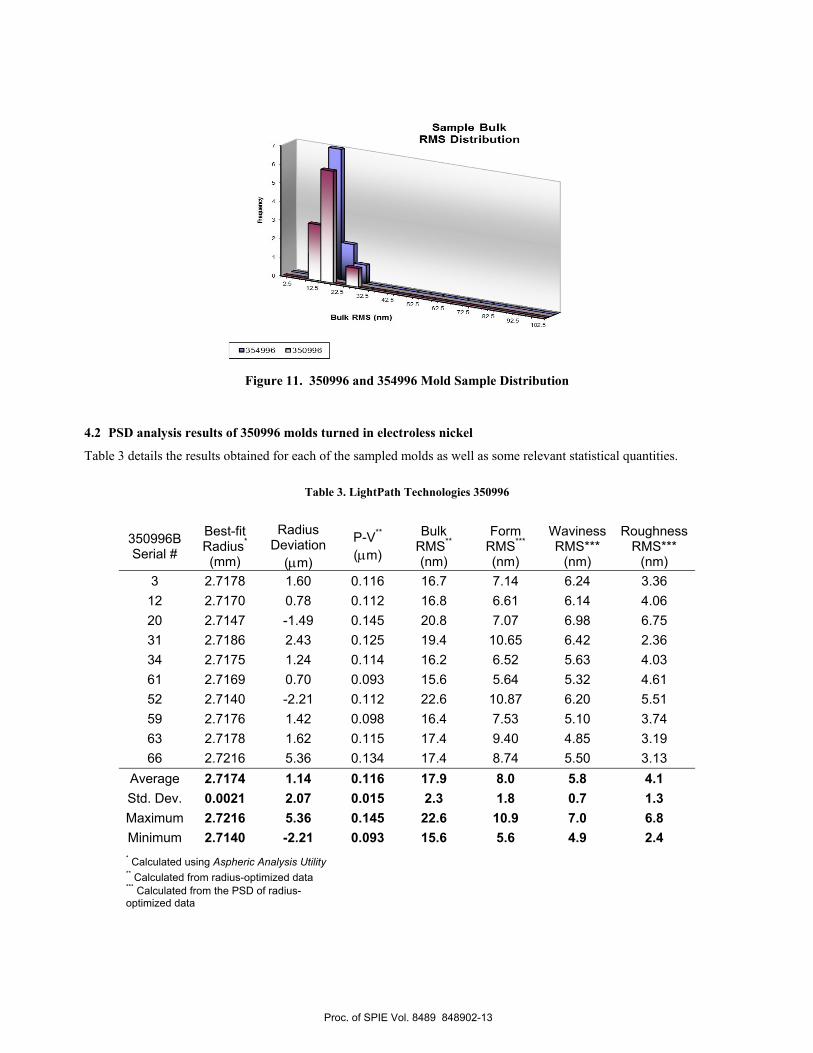
Mold fabrication was performed using LightPath Technologies’ production facilities using experienced machine operators. In the case of the 354996 molds, selected molds were pulled from quantities slated for production, while 350996 samples needed to be manufactured exclusively for this research, as the production of this lens ceased some years ago. Final mold selection for detailed analysis was based primarily on the similarity of bulk irregularity measurements. As shown in figure 11, the samples are fairly tightly distributed near the low side of the maximum bulk RMS specification (105.5 nm). Statistical averages and standard deviations of bulk RMS for each sample can be found below in tables 3 and 4.
Proc. of SPIE Vol. 8489 848902-12
Sample BulkRMS Distribution
102.5
M354996 e350996
Figure 11. 350996 and 354996 Mold Sample Distribution
4.2 PSD analysis results of 350996 molds turned in electroless nickel
Table 3 details the results obtained for each of the sampled molds as well as some relevant statistical quantities.
Average 2.6382 -1.42 0.106 14.5 6.0 5.4 3.1 Std. Dev. 0.0020 1.95 0.019 3.5 2.7 1.4 0.5 Maximum 2.6418 2.24 0.137 23.1 12.7 8.0 4.2 Minimum 2.6361 -3.46 0.078 10.3 3.1 3.7 2.4 * Calculated using Aspheric Analysis Utility ** Calculated from radius-optimized data *** Calculated from the PSD of radius-optimized data
4.4 Form, waviness, and roughness comparisons of 350996 and 354996
Contrary to expectation, very little difference has been revealed in the two surface types. Figures 12 and 13 illustrate the breakdown in RMS contribution for each sampled mold. Figure 14, shows a side-by-side comparison of average frequency band contribution for both surface types.
Figure 12. 350996 RMS Frequency Band Components of Sampled Molds
Proc. of SPIE Vol. 8489 848902-14
9.0
8.0
7.0
6.0
É 5.0cÑ 4.0
rc 3.0
2.0
0
0.0
350996 and 354996 Average RMS Contributions
Form RMS
354996B 350996BWaviness RMS
MoldRoughness RMS
30.0
25.0
20.0
I 15.0coE 10.0K
5.0
0.0
354996 RMS Contribution by Frequency Band
120 133 523 547 562 566 571 585 588 598
FomiRMS NWaaInessRMS oRoyghnessRMS Mold
Figure 13. 354996 RMS Frequency Band Components of Sampled Molds
Figure 14. RMS Frequency Band Component Comparison
However, when looking at the average fraction of RMS contribution for each mold type, one distinction does appear in the data. As shown in table 5, there is an ~5% reduction in form-RMS contribution of the carbide molds compared to the nickel molds. However, this reduction is bought at the expense of the waviness RMS, which is slightly higher in the carbide molds by approximately the same amount, and also displays in the standard deviation more than twice the variability. Interestingly, no meaningful differences are revealed in the roughness band.
Table 5. 350996 and 354996 Comparison
350996 Form RMS %
Waviness RMS %
Roughness RMS %
Average 44.6% 32.7% 22.7% Std. Dev. 7.2% 3.3% 5.9%
354996 Form RMS %
Waviness RMS %
Roughness RMS %
Average 40.0% 38.1% 21.9% Std. Dev. 8.4% 8.5% 4.7%
Proc. of SPIE Vol. 8489 848902-15
Of course, this analysis has been performed on a very limited sample size, and may not be a true representation of the statistical differences that may exist in a larger population. Furthermore, the imposed frequency band limits defining form, waviness, and roughness do obviously affect the final component RMS mix. Lastly, the 1-D PSD may be insufficient to fully describe the complete family of frequencies present, particularly on the ground surfaces which are known to contain greater waviness in the circumferential direction, which the 1-D analysis is not sensitive to. The results are most representative of a lens type that was transitioned in production from a diamond-turned fabrication step in nickel to a diamond ground fabrication step in carbide, and measured using tools commonly available in most fabrication shops. The topographic similarity in the two types is a testament to the great strides that have been made in the grinding of carbide molds to achieve similar optical performance to nickel molds.
5. CONCLUSIONS
SPDT and Diamond Grinding are both viable technologies for the fabrication of molds for precision molded optics. Each technology has its own manufacturing chain and presents unique advantages and potential pitfalls. Successful precision molded optics, whether injection molded plastic optics or precision glass molded optics, can be manufactured to a high level of precision using either technology.
Proc. of SPIE Vol. 8489 848902-16
REFERENCES
i Schaub, M.P., [The Design of Plastic Optical Systems], SPIE Press, Bellingham, Washington, (2009) ii Baumer, S., [Handbook of Plastic Optics], Wiley-VCH, Weinheim, Germany (2005). iii Schaub, M., Schwiegerling, J., Fest, E., Symmons, A., Shepard, R.H., [Molded Optics: Design and Manufacture], CRC Press, Taylor and Francis Group, London, Chapter 5: Molded Optics, 165-200 (2011) iv Symmons, A. and Pini R., “Precision molded glass challenges plastic optics”, Laser Focus World, July 2011 pg 42-45. v LightPath Technologies inc., ECO-550 Datasheet, 2010. vi Yazid E. Tohme, "Grinding aspheric and freeform micro-optical molds", Proc. SPIE 6462, 64620K (2007); http://dx.doi.org/10.1117/12.712706. vii Dini, J.W., “Perspective on plating for precision finishing”, Proceedings of ASPE Spring Topical Meeting on Metal Platings for Precision Finishing Operations, Tucson, AZ, 1991. viii Syn, C.K., et al., “Influence of Phosporus Content and Heat Treatment on the Machinability of Electroless Nickel Deposits”, Proceedings of the Electroless Nickel Conference IV, Chicago, IL, 1985. ix James E. Harvey and Anita K. Thompson, "Scattering effects from residual optical fabrication errors", Proc. SPIE 2576, 155 (1995); http://dx.doi.org/10.1117/12.215588. x The International Nickel Company Inc. (INCO), “The Engineering Properties of Electroless Nickel Deposits”, Revision A603, 75C 2-80 (2M 11-77) 5344, USA. xi www.matweb.com – Goodfellow Tungsten Carbide/Cobalt – (Captured from the internet 07/21/12). xii General Carbide, “The Designer’s Guide to Tungsten Carbide”, July 2008. Greensburg, PA, USA. xiii Gerchman, M. C., “Fundamental Axial Spindle Motions and Optical Tolerancing”, Rank Taylor Hobson Inc., Keene, NH 03431, USA xiv CDGM Optical Glass Catalog (Captured from the internet on 11/28/2011). xv LightPath Technologies inc., C0550 Low Melting Point Fusion Glass Datasheet. xvi LightPath Technologies Inc., Product Catalog, 2008. xvii H. Tobben, G. Ringle, F. Kratz, and D. R. Schmitt., “The Use of Power Spectral Density to Specify Optical Surfaces”, Deutsche Forschungsanstalt fur Luft- und Raumfahrt e. V. (DLR), Institut fur Flugfuhrung, Lilienthalplatz 7, D-38108 Braunschweig, Germany xviii J.K Lawson, C.R. Wolfe, K.R. Manes, J.B. Trenholme, D.M. Aikens, and R.E. English, Jr., “Specification of Optical Components using the Power Spectral Density Function”, Lawrence Livermore National Laboratory Livermore, CA, 94551, SPIE Vol. 2536 xix J.K Lawson, , D.M. Aikens, R.E. English, Jr., and C.R. Wolfe, “Power Spectral Density Specifications for High-Power Laser Systems”, Lawrence Livermore National Laboratory Livermore, CA, 94551, SPIE Vol. 2775 xx Sidick E., “Power Spectral Density Specification and Analysis of Large Optical Surfaces”, Jet Propulsion Laboratory, California Institute of Technology, 4800 Oak Grove Drive, Pasadena, CA, USA 91109, SPIE Vol. 7390 xxi R.N. Youngworth, B.B. Gallagher, and B.L. Stamper, “An Overview of Power Spectral Density (PSD) Calculations”, Ball Aerospace Corporation, SPIE Vol. 5869 xxii S.G. Alcock, G.D. Ludbrook, T. Owen, and R. Dockree, “Using the Power Spectral Density Method to Characterize the Surface Topography of Optical Surfaces”, Diamond Light Source Ltd, Didcot, Oxfordshire, OX11 0DE, UK, SPIE Vol. 7801 xxiii E. L. Church, “Fractal surface finish”, Applied Optics, Vol. 27, No. 8, pp. 1518-1526, 1988