Improve the performance of MOCVD grown GaN-on-Si HEMT structure Dr. Xiaoqing Xu Stanford Nanofabrication Facility Abstract The SNF installed a new metalorganic chemical vapor deposition (MOCVD) system for the growth of III-nitrides (i.e. GaN, AlN, InN). The capabilities of MOCVD have enhanced and propelled research of III-nitride in power electronics, optoelectronics, timing references, high frequency applications, and harsh environment sensors. One of the most powerful applications is in the fabrication of GaN HEMT which utilizes a two- dimensional electron gas (2DEG) layer that occurs at the interface of GaN and AlGaN. The properties of HEMTs are dependent on the sheet concentration and the electron mobility of the 2DEG layer. Our initial effort had developed a HEMT structure with the sheet carrier concentration, electron mobility, and sheet resistivity being 1.1x10 13 cm -2 , 1590 cm 2 /Vs, and 362 ohm/cm 2 , respectively. However, the sheet resistance variation over the 4” wafer was found to be 6%, which is higher than the Axitron specification (5%) of the tool. The goal of this project is to improve the uniformity of the electrical property to within 2.5% stdev% and thoroughly understand the dominant effects on HEMT performance and uniformity. High mobility uniformity with stdev% as low as 0.72% across the radius has been obtained on 4” wafer, and up to 1740.35 cm 2 /Vs 2DEG mobility has been realized with low C and O incorporation. The influencing effects: Al% and distribution in AlGaN barrier, growth temperature and distribution, C and O impurities, and back end metal contact annealing et al. are discussed. I. Introduction The main factors influencing AlGaN/GaN 2DEG concentration and mobility are: Al% in AlGaN barrier, AlGaN barrier thickness, AlN spacer thickness, GaN cap thickness,
Transcript
Improve the performance of MOCVD grown GaN-on-Si HEMT structure
Dr. Xiaoqing Xu
Stanford Nanofabrication Facility Abstract The SNF installed a new metalorganic chemical vapor deposition (MOCVD) system for
the growth of III-nitrides (i.e. GaN, AlN, InN). The capabilities of MOCVD have
enhanced and propelled research of III-nitride in power electronics, optoelectronics,
timing references, high frequency applications, and harsh environment sensors. One of
the most powerful applications is in the fabrication of GaN HEMT which utilizes a two-
dimensional electron gas (2DEG) layer that occurs at the interface of GaN and AlGaN.
The properties of HEMTs are dependent on the sheet concentration and the electron
mobility of the 2DEG layer.
Our initial effort had developed a HEMT structure with the sheet carrier concentration,
electron mobility, and sheet resistivity being 1.1x1013 cm-2, 1590 cm2/Vs, and 362
ohm/cm2, respectively. However, the sheet resistance variation over the 4” wafer was
found to be 6%, which is higher than the Axitron specification (5%) of the tool. The goal
of this project is to improve the uniformity of the electrical property to within 2.5%
stdev% and thoroughly understand the dominant effects on HEMT performance and
uniformity. High mobility uniformity with stdev% as low as 0.72% across the radius has
been obtained on 4” wafer, and up to 1740.35 cm2/Vs 2DEG mobility has been realized
with low C and O incorporation. The influencing effects: Al% and distribution in AlGaN
barrier, growth temperature and distribution, C and O impurities, and back end metal
contact annealing et al. are discussed.
I. Introduction
The main factors influencing AlGaN/GaN 2DEG concentration and mobility are: Al%
in AlGaN barrier, AlGaN barrier thickness, AlN spacer thickness, GaN cap thickness,
and C% in GaN layer, all dependent on the growth temperature and its distribution.
Table I is a summary of the preceding results in literature. Fig.1~Fig. 4 are copies of the
corresponding plots1-3.
Table I Main factors influencing AlGaN/GaN 2DEG concentration and mobility
Al% in AlGaN
barrier AlGaN barrier
thickness AlN spacer thickness
GaN cap thickness
C% in GaN
Range 15%-90% 5-30nm 0-2nm 0.1-10nm 2e16-2e18 cm-2
2DEG concentration
↑ ↑ ↓ ↓ ↓
Electron mobility
↓ ↓ ↑ ↑ ↓
Fig. 11 Dependence of 2DEG layer concentration (left scale) and mobility (right scale) on (a) various barrier thickness values when Al%=0.3 and (b) Al% in the barrier layer. Dashed lines, mobility limited only by phonon scattering (polar and acoustic phonons).
Fig. 21 (a) Dependence of 2DEG layer concentration on AlN layer width at various barrier doping. (1) Without doping, (2) with doping,1019 cm-3. (b) Dependence of 2DEG mobility on AlN layer width at various barrier doping.
Fig. 32 (a) The 2DEG sheet density and (b) the mobility at 300K for the GaN/AlGaN/GaN HEMT as a function of GaN capping layer thickness with: the AlN barrier thickness is 35Å; and the Al0.32Ga0.68N barrier thickness is 200Å. Symbols represent experimental data from literature.
Fig. 43 (a) The carbon concentration versus growth temperature in GaN layer, (b) 2DEG mobility and carrier density in the Al0.28Ga0.72N/GaN heterostructures as a function of growth temperature.
Overall consideration, our HEMT growth structure is designed as Fig. 5. In this report,
we will focus on four dominant effects: 1. 2DEG mobility uniformity across 4” wafer,
which is a combined effect of Al% and thickness distributions in AlGaN barrier, AlN
spacer and GaN cap thickness distributions, and C% distribution in GaN layer, all
dependent on the growth temperature and its distribution; 2. Influence of C and O
impurity incorporation on the 2DEG mobility; 3. Influence of Al% in AlGaN barrier on the
2DEG performance; 4. Influence of metal contact annealing on the HEMT structure
performance.
Fig. 5 GaN-on-Si HEMT structure
II. Methodology and results
1. 2DEG mobility uniformity across 4” wafer
a. Influence of growth temperature on Al%
While the 5 parameters, Al% and thickness distributions in AlGaN barrier, AlN spacer
and GaN cap thickness distributions, C% in GaN layer, are all dependent on the growth
temperature and its distribution, it is hard and destructive to precisely determine the
thickness distribution of such thin layers (1~25nm) and the C impurity elemental
mapping of low concentration (down to 1x1016cm-3). The Al% distribution, however, can
be determined nondestructively by photoluminescence (PL) mapping. The Al%
distribution, is an indication of the growth temperature distribution, and thus can be a
representative of all the 5 parameters.
To test the growth temperature dependence of Al%, we grow 3 AlGaN/AlN/Si testing
samples at 1000 oC, 1040 oC, and 1080 oC (sample surface temperature), respectively.
Fig. 6(a)~(c) show the PL mappings of the three samples, and Fig. 6(d) plots the growth
temperature dependence of Al%. It’s found that the Al% is highly dependent on the
growth temperature variation, 0.24%Al increment per oC shift, at the commonly used
temperature range, 1000~1080 oC.
Si (111)
AlN
Al0.8Ga0.2N
Al0.5Ga0.5N
1.2µm GaN
Al0.2Ga0.8N
25nm Al0.25Ga0.75N barrier 1nm AlN spacer
3nm GaN cap
(a) 1000 oC (b) 1040 oC
(c) 1080 oC (d)
Fig. 6 AlGaN/AlN/Si testing samples grown at (a) 1000 oC, (b) 1040 oC, and (c) 1080 oC, respectively, (d) The growth temperature dependence of Al%, 0.24%Al/oC.
b. Tuning growth temperatures for high uniformity
Table II Growth temperatures and heating zone power percentages of the top 4 layers
There are three heating zones, A, B, and C, as illustrated in Fig. 7(a). Due to the strain
variation and the wafer bow development as the film layers are increased, it is much
harder to control the uniformity of the full HEMT structure than the simple AlGaN/AlN/Si
test structure. After many tunings of the three heating zone power percentages in the
top 4 layers, the settings in Table II (the sample surface temperatures of different layers
are read out from Fig. 7(b)) result in a good Al% uniformity, 2.4% stdev% at 25%
average Al%, and a good thickness uniformity, 3.2% stdev% at 2.76µm average
thickness of the full GaN-on-Si HEMT structure. The PL mapping of the resulting AlxGa1-
xN barrier and the thickness mapping of the full HEMT structure are shown on Fig. 8(a)
and 8(b).
Fig. 7 (a) Heater coils: Zone A: Centre (red), Zone B: Middle (orange), Zone C: Outside (blue), (b) Sample surface temperature measured by in-situ EpiTT pyrometer.
Fig. 8 (a) The PL mapping of the AlxGa1-xN barrier and (b) the thickness mapping of the full HEMT.
c. High uniformity of 2DEG mobility achieved on 4” wafer
LT-AlN
Al0.8Ga0.2N/Al0.5Ga0.5N/Al0.2Ga0.8N
AlN/ AlxGa1-xN /GaN cap
HT-AlN
GaN -1st
GaN -2nd
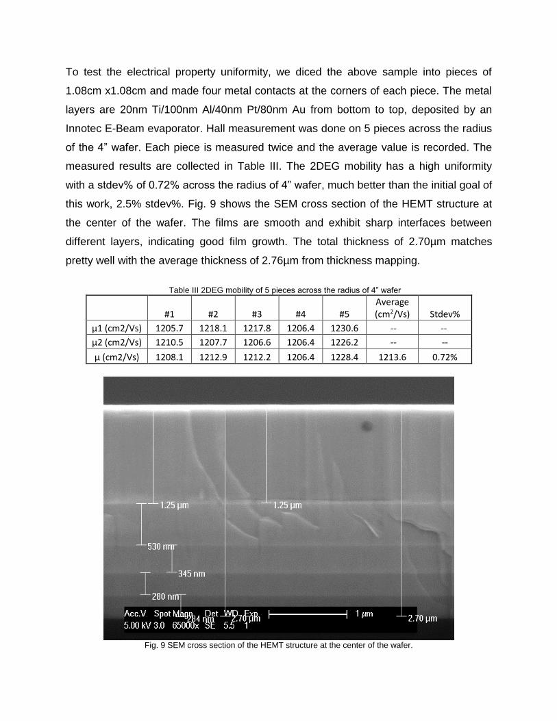
To test the electrical property uniformity, we diced the above sample into pieces of
1.08cm x1.08cm and made four metal contacts at the corners of each piece. The metal
layers are 20nm Ti/100nm Al/40nm Pt/80nm Au from bottom to top, deposited by an
Innotec E-Beam evaporator. Hall measurement was done on 5 pieces across the radius
of the 4” wafer. Each piece is measured twice and the average value is recorded. The
measured results are collected in Table III. The 2DEG mobility has a high uniformity
with a stdev% of 0.72% across the radius of 4” wafer, much better than the initial goal of
this work, 2.5% stdev%. Fig. 9 shows the SEM cross section of the HEMT structure at
the center of the wafer. The films are smooth and exhibit sharp interfaces between
different layers, indicating good film growth. The total thickness of 2.70µm matches
pretty well with the average thickness of 2.76µm from thickness mapping.
Table III 2DEG mobility of 5 pieces across the radius of 4” wafer
Fig. 9 SEM cross section of the HEMT structure at the center of the wafer.
2. Influence of C and O incorporation on the 2DEG mobility
Table IV 2DEG performances of samples with different C and O concentrations
Mobility (cm2/Vs)
Sheet Number
(cm-2)
Sheet Resistance (ohm/cm2)
A 1740.35 9.3368E+12 384.135
B 1224.6 1.2902E+13 395.04
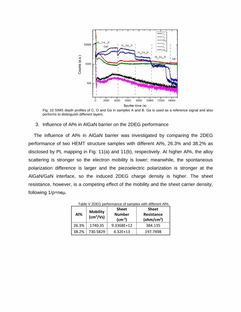
The C and O impurity incorporation in the vicinity of the 2DEG channel can severely
affect the 2DEG performance especially when the concentration is higher than
1x1017cm-3. Table IV shows the different performance of two HEMT structures with very
similar film parameters except for the C and O concentrations. It’s noted that as high as
1740.35 cm2/Vs electron mobility was achieved on sample A, while sample B has lower
mobility and higher sheet carrier density. The SIMS data of Ga, C, and O for samples A
and B are compared in Fig. 10.
The SIMS depth profiles were measured by a NanoSIMS with Cs ions along all the epi
layers. It’s noted that due to the fact of low depth resolution of NanoSIMS, although
perfect surface resolution, the interfaces between the layers are not very sharp. The
ultra-high C and O signals at the surface are a combined effect of surface molecules
absorption and instable ion yields, so can be disregarded. Despite of the limitations of
the measurement, sample B obviously has higher C and O signals in all the epi layers.
This explains the lower mobility of sample B by enhanced trapping effect and ionized
impurity scattering at higher impurities incorporation. It’s also noted that sample B has
higher sheet carrier density than sample A, so the dominant impurity in sample B is O
other than C since O is a donor while C is an acceptor in GaN.
Therefore, to obtain high 2DEG performance, growth temperature of the GaN layer
needs to be high enough and reactor condition including pretreatment and de-
contamination processes needs to be controlled to reduce C and O incorporation.
Fig. 10 SIMS depth profiles of C, O and Ga in samples A and B. Ga is used as a reference signal and also performs to distinguish different layers.
3. Influence of Al% in AlGaN barrier on the 2DEG performance
The influence of Al% in AlGaN barrier was investigated by comparing the 2DEG
performance of two HEMT structure samples with different Al%, 26.3% and 38.2% as
disclosed by PL mapping in Fig. 11(a) and 11(b), respectively. At higher Al%, the alloy
scattering is stronger so the electron mobility is lower; meanwhile, the spontaneous
polarization difference is larger and the piezoelectric polarization is stronger at the
AlGaN/GaN interface, so the induced 2DEG charge density is higher. The sheet
resistance, however, is a competing effect of the mobility and the sheet carrier density,
following 1/ρ=neµ.
Table V 2DEG performance of samples with different Al%
Al% Mobility (cm2/Vs)
Sheet Number
(cm-2)
Sheet Resistance (ohm/cm2)
26.3% 1740.35 9.3368E+12 384.135
38.2% 730.5829 4.32E+13 197.7498
Fig. 11 PL mapping of HEMT structure samples at different barrier Al%, (a) 26.3% and (b) 38.2%.
4. Influence of metal contact annealing on the HEMT structure performance
The influence of metal contact annealing on the HEMT structure performance was
investigated by measuring I-V curve and Hall data of samples annealed at different
temperatures. After depositing the metal layers, 20nm Ti/100nm Al/40nm Pt/80nm Au,
and sample dicing, the pieces were annealed in an RTA at 550oC~850oC in N2
environment. I-V measurement was done between two adjacent metal contacts of the
1.08 cm x1.08 cm pieces. The I-V curves are shown on Fig. 12(a). It’s found that the I-V
curves are not exactly linear until 850oC annealing, and the higher the annealing
temperature is, the higher the current is (the lower the resistance is). The inset is a
magnification of the I-V curve at low voltage. Although the I-V curves below 850oC
annealing are not perfectly linear, they are almost linear at low voltage range as was
shown in the inset, indicating near ohmic contact for all the samples at -0.1V~0.1V.
The Hall measurement was done within the linear region, and the contact annealing
temperature dependences of the 2DEG mobility, sheet resistance, and sheet number
are shown on Fig. 12(b). At higher annealing temperature, the carrier sheet density is
increased while the 2DEG mobility is decreased. Therefore, although the ohmic contact
seems to be improved after annealing, the 2DEG mobility of the HEMT structure, is
actually degraded. The increased carrier density and current are due to the doping
effect of the metals which could have diffused into the 2DEG layer at high temperatures,
or the C/O et. al. impurities are activated at high temperature treatment. Therefore, the
as prepared sample exhibits the highest mobility while the 850oC annealed sample
exhibit the lowest mobility, although highest current. The mechanism behind this is still
to be verified.
Fig. 12 (a) I-V curves between two adjacent metal contacts of the 1.08 cm x1.08 cm Hall samples annealed at different temperatures. The inset is a magnification of the I-V curve at low voltage. (b) Contact annealing temperature dependences of the 2DEG mobility, sheet resistance, and sheet number.
III. Summary and future work In summary, we have successfully achieved high uniformity of 2DEG mobility with
stdev% as low as 0.72% across the radius of the 4” GaN-on-Si HEMT wafer, and up to
1740.35 cm2/Vs 2DEG mobility has been realized. The dominant effects on 2DEG
performance and uniformity are deeply investigated and understood.
For future work, the influence of C and O impurity on the back end contact property, and
the influence of possible metal diffusion during high temperature annealing on the
2DEG performance need to be further investigated and verified. The growth condition
needs to be strictly controlled, including sample cleaning, reactor pretreatment and de-
contamination, and carrier wafer selection, to limit the C and O incorporation.
IV. Acknowledgement • Thanks to Dr. Ryan Zhong from Aixtron for the valuable advices and fruitful discussions on the HEMT growth and back end processes; • Thanks to Dr. Zhiqiang Li and Torsten Stoll from Nanometrics for the measurement of PL mapping and thickness mapping; • Thanks to Chuck Hitzman from Stanford Nano Shared Facility for NanoSIMS measurement;
• Thanks to the Stanford students, Caitlin Chapin, Seonghyun Paik, Jieyang Jia, Ateeq Suria, and Sam Falkenhagen for their help on the contact processing, thickness measurement, Hall measurement et. al; • This work is supported by Stanford Nanofabrication Facility as a community service project V. References [1] Karine Abgaryan, Ilya Mutigullin, and Dmitry Reviznikov. Theoretical investigation of 2DEG concentration and mobility in the AlGaN/GaN heterostructures with various Al concentrations. Phys. Status Solidi C 12, No. 12, 1376–1382 (2015). [2] A. Asgari, M. Kalafi, L. Faraone. The effects of GaN capping layer thickness on two-dimensional electron mobility in GaN/AlGaN/GaN heterostructures. Physica E 25, 431–437 (2005). [3] Jr-Tai Chen, Urban Forsberg, and Erik Janzen. Impact of residual carbon on two-dimensional electron gas properties in AlxGa1-xN/GaN heterostructure.