Improved growth of GaN layers on ultra thin silicon nitride/Si (1 1 1) by RF-MBE Mahesh Kumar a,b , Basanta Roul a,b , Thirumaleshwara N. Bhat a , Mohana K. Rajpalke a , P. Misra c , L.M. Kukreja c , Neeraj Sinha d , A.T. Kalghatgi b , S.B. Krupanidhi a, * a Materials Research Centre, Indian Institute of Science, Bangalore 560012, India b Central Research Laboratory, Bharat Electronics, Bangalore 560013, India c Laser Materials Processing Division, Raja Ramanna Centre for Advanced Technology, Indore 452013, India d Office of Principal Scientific Advisor, Government of India, New Delhi 110011, India 1. Introduction GaN material system is gathering great interest from the viewpoint of its application to optical devices as well as electronic devices because of its wide band gap nature [1]. A number of studies have been performed successfully to grow GaN on different substrates such as Al 2 O 3 [2], SiC [3], and Si [4]. Among these materials silicon is viewed as one of the most promising candidates for the GaN epitaxy because of its many advantages such as high- quality, large size, low cost and a well-known existing device technology [5]. However, three-dimensional (3D) island growth is unavoidable for the direct growth of GaN on Si (1 1 1) because of the extreme lattice and thermal expansion coefficient mismatch between the GaN and the Si substrate. Although some results have been reported on the successful growth of GaN on Si using AlN [6,7], SiC [8,9] and InGaN [10] buffer layers, but a defect-induced yellow luminescence (YL) was commonly present, which affects the optical properties of GaN greatly. On the other hand, it has been demonstrated that no YL was present when a silicon nitride buffer layer was used for the GaN growth [11–13]. The present work envisages a comparative study of the GaN growth by RF-MBE on Si (1 1 1) as a function of nitridation time and temperature. We have grown a high quality, less stressed and optically excellent GaN films using a new growth approach. 2. Experiment The growth system used in this study was a RF-MBE system (OMICRON) equipped with a radio frequency (RF) plasma source. The base pressure in the system was below 1 10 10 mbar. The undoped Si (1 1 1) substrates were ultrasonically degreased in isopropyl alcohol (IPA) for 10 min and boiled in trichloroethylene, acetone and methanol at 70 8C for 5 min, respectively, followed by dipping in 5% HF to remove the surface oxide. The substrates were outgassed at 900 8C for 1 h in ultra-high vacuum. In sample (a)–(d) the nitridation of the substrate was carried out at 530 and 700 8C for nitridation times from 0 to 60 min as shown in Table 1. In sample (e) the new growth process sequence was employed in which the nitridation of the substrate was carried out at 530 8C for 30 min followed by annealing at 900 8C for 30 min and again nitridation at 700 8C for 30 min. For all samples, low-temperature GaN buffer layers of thickness of 20 nm were grown at 500 8C after nitridation, where the gallium (Ga) effusion cell temperature was kept at 950 8C and corresponding beam equivalent pressure (BEP) was maintained of 5.6 10 7 mbar. Afterwards, a GaN epilayers of thickness of 225 nm were grown on the buffer layer at 700 8C. Nitrogen flow rate and plasma power were kept at 0.5 sccm and 350 W, respectively for the nitridation, buffer layer and subse- quent GaN growth. The structural characterization and surface Materials Research Bulletin 45 (2010) 1581–1585 ARTICLE INFO Article history: Received 25 May 2010 Received in revised form 15 July 2010 Accepted 23 July 2010 Available online 1 August 2010 Keywords: A. Nitrides B. Epitaxial growth B. Luminescence C. X-ray diffraction ABSTRACT High-quality GaN epilayers were grown on Si (1 1 1) substrates by molecular beam epitaxy using a new growth process sequence which involved a substrate nitridation at low temperatures, annealing at high temperatures, followed by nitridation at high temperatures, deposition of a low-temperature buffer layer, and a high-temperature overgrowth. The material quality of the GaN films was also investigated as a function of nitridation time and temperature. Crystallinity and surface roughness of GaN was found to improve when the Si substrate was treated under the new growth process sequence. Micro-Raman and photoluminescence (PL) measurement results indicate that the GaN film grown by the new process sequence has less tensile stress and optically good. The surface and interface structures of an ultra thin silicon nitride film grown on the Si surface are investigated by core-level photoelectron spectroscopy and it clearly indicates that the quality of silicon nitride notably affects the properties of GaN growth. ß 2010 Elsevier Ltd. All rights reserved. * Corresponding author. Tel.: +91 80 22932943; fax: +91 80 23607316. E-mail address: [email protected](S.B. Krupanidhi). Contents lists available at ScienceDirect Materials Research Bulletin journal homepage: www.elsevier.com/locate/matresbu 0025-5408/$ – see front matter ß 2010 Elsevier Ltd. All rights reserved. doi:10.1016/j.materresbull.2010.07.025
Transcript
Materials Research Bulletin 45 (2010) 1581–1585
Improved growth of GaN layers on ultra thin silicon nitride/Si (1 1 1) by RF-MBE
Mahesh Kumar a,b, Basanta Roul a,b, Thirumaleshwara N. Bhat a, Mohana K. Rajpalke a, P. Misra c,L.M. Kukreja c, Neeraj Sinha d, A.T. Kalghatgi b, S.B. Krupanidhi a,*a Materials Research Centre, Indian Institute of Science, Bangalore 560012, Indiab Central Research Laboratory, Bharat Electronics, Bangalore 560013, Indiac Laser Materials Processing Division, Raja Ramanna Centre for Advanced Technology, Indore 452013, Indiad Office of Principal Scientific Advisor, Government of India, New Delhi 110011, India
A R T I C L E I N F O
Article history:
Received 25 May 2010
Received in revised form 15 July 2010
Accepted 23 July 2010
Available online 1 August 2010
Keywords:
A. Nitrides
B. Epitaxial growth
B. Luminescence
C. X-ray diffraction
A B S T R A C T
High-quality GaN epilayers were grown on Si (1 1 1) substrates by molecular beam epitaxy using a new
growth process sequence which involved a substrate nitridation at low temperatures, annealing at high
temperatures, followed by nitridation at high temperatures, deposition of a low-temperature buffer
layer, and a high-temperature overgrowth. The material quality of the GaN films was also investigated as
a function of nitridation time and temperature. Crystallinity and surface roughness of GaN was found to
improve when the Si substrate was treated under the new growth process sequence. Micro-Raman and
photoluminescence (PL) measurement results indicate that the GaN film grown by the new process
sequence has less tensile stress and optically good. The surface and interface structures of an ultra thin
silicon nitride film grown on the Si surface are investigated by core-level photoelectron spectroscopy and
it clearly indicates that the quality of silicon nitride notably affects the properties of GaN growth.
� 2010 Elsevier Ltd. All rights reserved.
Contents lists available at ScienceDirect
Materials Research Bulletin
journa l homepage: www.e lsev ier .com/ locate /mat resbu
1. Introduction
GaN material system is gathering great interest from theviewpoint of its application to optical devices as well as electronicdevices because of its wide band gap nature [1]. A number ofstudies have been performed successfully to grow GaN on differentsubstrates such as Al2O3 [2], SiC [3], and Si [4]. Among thesematerials silicon is viewed as one of the most promising candidatesfor the GaN epitaxy because of its many advantages such as high-quality, large size, low cost and a well-known existing devicetechnology [5]. However, three-dimensional (3D) island growth isunavoidable for the direct growth of GaN on Si (1 1 1) because ofthe extreme lattice and thermal expansion coefficient mismatchbetween the GaN and the Si substrate. Although some results havebeen reported on the successful growth of GaN on Si using AlN[6,7], SiC [8,9] and InGaN [10] buffer layers, but a defect-inducedyellow luminescence (YL) was commonly present, which affectsthe optical properties of GaN greatly. On the other hand, it has beendemonstrated that no YL was present when a silicon nitride bufferlayer was used for the GaN growth [11–13]. The present workenvisages a comparative study of the GaN growth by RF-MBE on Si(1 1 1) as a function of nitridation time and temperature. We have
0025-5408/$ – see front matter � 2010 Elsevier Ltd. All rights reserved.
doi:10.1016/j.materresbull.2010.07.025
grown a high quality, less stressed and optically excellent GaNfilms using a new growth approach.
2. Experiment
The growth system used in this study was a RF-MBE system(OMICRON) equipped with a radio frequency (RF) plasma source.The base pressure in the system was below 1 � 10�10 mbar. Theundoped Si (1 1 1) substrates were ultrasonically degreased inisopropyl alcohol (IPA) for 10 min and boiled in trichloroethylene,acetone and methanol at 70 8C for 5 min, respectively, followed bydipping in 5% HF to remove the surface oxide. The substrates wereoutgassed at 900 8C for 1 h in ultra-high vacuum. In sample (a)–(d)the nitridation of the substrate was carried out at 530 and 700 8Cfor nitridation times from 0 to 60 min as shown in Table 1. Insample (e) the new growth process sequence was employed inwhich the nitridation of the substrate was carried out at 530 8C for30 min followed by annealing at 900 8C for 30 min and againnitridation at 700 8C for 30 min. For all samples, low-temperatureGaN buffer layers of thickness of 20 nm were grown at 500 8C afternitridation, where the gallium (Ga) effusion cell temperature waskept at 950 8C and corresponding beam equivalent pressure (BEP)was maintained of 5.6 � 10�7 mbar. Afterwards, a GaN epilayers ofthickness of 225 nm were grown on the buffer layer at 700 8C.Nitrogen flow rate and plasma power were kept at 0.5 sccm and350 W, respectively for the nitridation, buffer layer and subse-quent GaN growth. The structural characterization and surface
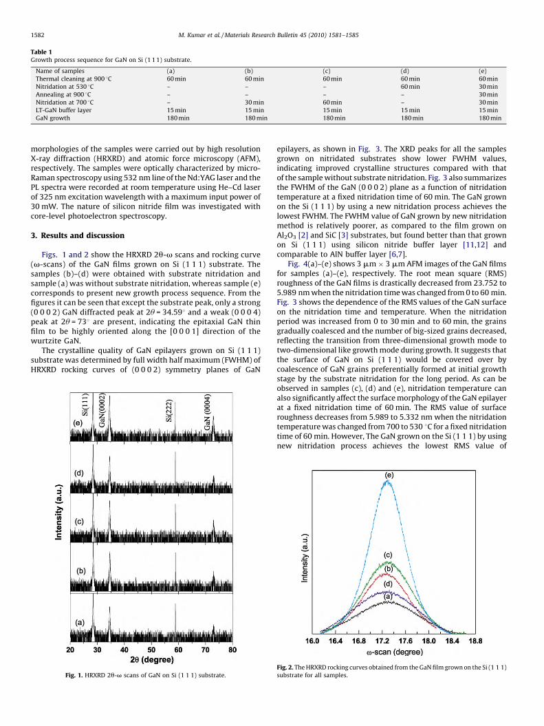
Table 1Growth process sequence for GaN on Si (1 1 1) substrate.
Name of samples (a) (b) (c) (d) (e)
Thermal cleaning at 900 8C 60 min 60 min 60 min 60 min 60 min
Nitridation at 530 8C – – – 60 min 30 min
Annealing at 900 8C – – – – 30 min
Nitridation at 700 8C – 30 min 60 min – 30 min
LT-GaN buffer layer 15 min 15 min 15 min 15 min 15 min
GaN growth 180 min 180 min 180 min 180 min 180 min
M. Kumar et al. / Materials Research Bulletin 45 (2010) 1581–15851582
morphologies of the samples were carried out by high resolutionX-ray diffraction (HRXRD) and atomic force microscopy (AFM),respectively. The samples were optically characterized by micro-Raman spectroscopy using 532 nm line of the Nd:YAG laser and thePL spectra were recorded at room temperature using He–Cd laserof 325 nm excitation wavelength with a maximum input power of30 mW. The nature of silicon nitride film was investigated withcore-level photoelectron spectroscopy.
3. Results and discussion
Figs. 1 and 2 show the HRXRD 2u-v scans and rocking curve(v-scans) of the GaN films grown on Si (1 1 1) substrate. Thesamples (b)–(d) were obtained with substrate nitridation andsample (a) was without substrate nitridation, whereas sample (e)corresponds to present new growth process sequence. From thefigures it can be seen that except the substrate peak, only a strong(0 0 0 2) GaN diffracted peak at 2u = 34.598 and a weak (0 0 0 4)peak at 2u = 738 are present, indicating the epitaxial GaN thinfilm to be highly oriented along the [0 0 0 1] direction of thewurtzite GaN.
The crystalline quality of GaN epilayers grown on Si (1 1 1)substrate was determined by full width half maximum (FWHM) ofHRXRD rocking curves of (0 0 0 2) symmetry planes of GaN
[(Fig._1)TD$FIG]
Fig. 1. HRXRD 2u-v scans of GaN on Si (1 1 1) substrate.
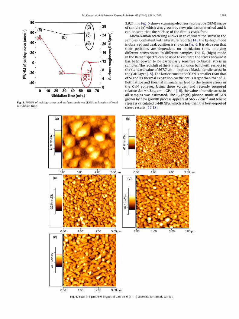
epilayers, as shown in Fig. 3. The XRD peaks for all the samplesgrown on nitridated substrates show lower FWHM values,indicating improved crystalline structures compared with thatof the sample without substrate nitridation. Fig. 3 also summarizesthe FWHM of the GaN (0 0 0 2) plane as a function of nitridationtemperature at a fixed nitridation time of 60 min. The GaN grownon the Si (1 1 1) by using a new nitridation process achieves thelowest FWHM. The FWHM value of GaN grown by new nitridationmethod is relatively poorer, as compared to the film grown onAl2O3 [2] and SiC [3] substrates, but found better than that grownon Si (1 1 1) using silicon nitride buffer layer [11,12] andcomparable to AlN buffer layer [6,7].
Fig. 4(a)–(e) shows 3 mm � 3 mm AFM images of the GaN filmsfor samples (a)–(e), respectively. The root mean square (RMS)roughness of the GaN films is drastically decreased from 23.752 to5.989 nm when the nitridation time was changed from 0 to 60 min.Fig. 3 shows the dependence of the RMS values of the GaN surfaceon the nitridation time and temperature. When the nitridationperiod was increased from 0 to 30 min and to 60 min, the grainsgradually coalesced and the number of big-sized grains decreased,reflecting the transition from three-dimensional growth mode totwo-dimensional like growth mode during growth. It suggests thatthe surface of GaN on Si (1 1 1) would be covered over bycoalescence of GaN grains preferentially formed at initial growthstage by the substrate nitridation for the long period. As can beobserved in samples (c), (d) and (e), nitridation temperature canalso significantly affect the surface morphology of the GaN epilayerat a fixed nitridation time of 60 min. The RMS value of surfaceroughness decreases from 5.989 to 5.332 nm when the nitridationtemperature was changed from 700 to 530 8C for a fixed nitridationtime of 60 min. However, The GaN grown on the Si (1 1 1) by usingnew nitridation process achieves the lowest RMS value of
[(Fig._2)TD$FIG]
Fig. 2. The HRXRD rocking curves obtained from the GaN film grown on the Si (1 1 1)
substrate for all samples.
[(Fig._3)TD$FIG]
Fig. 3. FWHM of rocking curves and surface roughness (RMS) as function of total
nitridation time.
[(Fig._4)TD$FIG]
Fig. 4. 3 mm � 3 mm AFM images of GaN on
M. Kumar et al. / Materials Research Bulletin 45 (2010) 1581–1585 1583
3.921 nm. Fig. 5 shows scanning electron microscope (SEM) imageof sample (e) which was grown by new nitridation method and itcan be seen that the surface of the film is crack free.
Micro-Raman scattering allows us to estimate the stress in thesamples. Consistent with literature reports [14], the E2-high modeis observed and peak position is shown in Fig. 6. It is also seen thattheir positions are dependent on nitridation time, implyingdifferent stress states in different samples. The E2 (high) modein the Raman spectra can be used to estimate the stress because ithas been proven to be particularly sensitive to biaxial stress insamples. The red shift of the E2 (high) phonon band with respect tothe standard value of 567.7 cm�1 implies a biaxial tensile stress inthe GaN layer [15]. The lattice constant of GaN is smaller than thatof Si and its thermal expansion coefficient is larger than that of Si.Both lattice and thermal mismatches lead to the tensile stress inthe GaN epilayer. Using these values, and recently proposedrelation Dv = 4.3sxx cm�1 GPa�1 [16], the value of tensile stress inall samples was estimated. The E2 (high) phonon mode of GaNgrown by new growth process appears at 565.77 cm�1 and tensilestress is calculated 0.448 GPa, which is less than the best-reportedstress results [17,18].
Si (1 1 1) substrate for sample (a)–(e).
[(Fig._5)TD$FIG]
Fig. 5. SEM image of sample (e), which shows crack free GaN layers.
[(Fig._7)TD$FIG]
Fig. 7. Room temperature PL spectra of GaN on Si (1 1 1). First inset shows FWHM of
PL spectra and second shows the luminescent band gaps of the GaN vs. the
corresponding stresses, the solid line represents a linear fitting result to the
experimental data.
[(Fig._8)TD$FIG]
M. Kumar et al. / Materials Research Bulletin 45 (2010) 1581–15851584
The optical properties of these samples were characterized byPL measurement using a He–Cd laser as the excitation source atroom temperature as shown in Fig. 7. From inset it can be seen thatFWHM of PL spectra decreases with increasing nitridation time atfixed temperature of 700 8C but nitridation at low temperature(530 8C) resulting inferior optical properties. The GaN film grownby new growth process reveals a strong near band-edge emissionpeak at 3.433 eV with lowest FWHM. The PL spectrum at 10 K ofGaN layers grown by the new growth process sequence is shown inFig. 8 which contains the near band emission (NBE) at 3.442 eVand donor–acceptor pair (DAP) peak at 3.292 eV and a fewlongitudinal optical (LO) phonon replicas of DAP spaced by 91 meVestablishing good optical quality of present GaN films. Thebroadband emission peaks in the long wavelength regionsnormally due to Ga vacancies and deep level impurities arepresent only for sample without nitridation.
It is known that the energy band gap of a semiconductor isaffected by the residual stress in film and a tensile stress will resultin a decrease of energy band gap. The inset in Fig. 7 describes theluminescent band gap as represented by the PL peak positionsversus residual stress in film for all five samples. An approximatelinear dependence is observed. By least-square fitting of the data,
[(Fig._6)TD$FIG]
Fig. 6. Room temperature micro-Raman spectra of GaN.
the band gap of GaN at room temperature can be expressed interms of biaxial stress according to
Eg ¼ 3:44234� 0:01982sxx ðeVÞ (1)
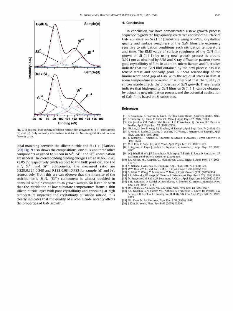
It is important to know the sources for better quality of wurtziteGaN grown on Si (1 1 1) by new growth process. The core-levelsphotoelectron spectroscopy was carried out to determine thechemical bonding states of silicon nitride surface using Al Karadiation (hn = 1486.6 eV). In Fig. 9 Si 2p core-level spectra (CLS)were recorded for sample (d) and (e) and it shows how annealingeffects the Si 2p surface sensitive core-level spectra. The CLS havebeen numerically fitted using Lorentzian convoluted with aGaussian functions. The background has been taken into accountusing a linear profile. In stoichiometric silicon nitride a Si atom isbonded to 4 N atoms (Si4+) and an N atom is bonded to 3 Si atoms[19], thus only the component with Si4+ is expected. At theinterface two more coordinations are required (Si3+ and Si1+) for an
Fig. 8. PL spectra of GaN at 10 K grown by new nitridation method (sample (e)).
[(Fig._9)TD$FIG]
Fig. 9. Si 2p core-level spectra of silicon nitride film grown on Si (1 1 1) for sample
(d) and (e). Only intensity attenuation is detected. No energy shift and no new
features arise.
M. Kumar et al. / Materials Research Bulletin 45 (2010) 1581–1585 1585
ideal matching between the silicon nitride and Si (1 1 1) lattices[20]. Fig. 9 also shows the compositions: one bulk and three othercomponents assigned to silicon in Si1+, Si3+ and Si4+ coordinationare needed. The corresponding binding energies are at +0.66, +2.20,+3.05 eV respectively (with respect to the bulk position). For theSi1+, Si3+ and Si4+ components, the measured ratio are0.328:0.324:0.348 and 0.133:0.084:0.783 for sample (d) and (e),respectively. From this we can observe that the intensity of thestoichiometric Si3N4 (Si4+) component is almost doubled inannealed sample compare to as grown sample. So it can be seenthat the nitridation at low substrate temperatures forms a thinsilicon nitride layer with poor crystallinity and annealing at hightemperature improved the crystallinity of silicon nitride. It isclearly indicates that the quality of silicon nitride notably affectsthe properties of GaN growth.
4. Conclusion
In conclusion, we have demonstrated a new growth processsequence to grow the high quality, crack free and smooth surface ofGaN epilayers on Si (1 1 1) substrate using RF-MBE. Crystallinequality and surface roughness of the GaN films are extremelysensitive to nitridation conditions such nitridation temperatureand time. The RMS value of surface roughness of the GaN filmgrown on Si (1 1 1) by using new growth process is around3.921 nm as obtained by AFM and X-ray diffraction pattern showsgood crystallinity of film. In addition, micro-Raman and PL studiesindicate that the GaN film obtained by the new process has lesstensile stress and optically good. A linear relationship of theluminescent band gap of GaN with the residual stress in film atroom temperature is observed. It is observed that the quality ofsilicon nitride affects the properties of GaN growth. These resultsindicate that high-quality GaN films on Si (1 1 1) can be obtainedby using the new nitridation process, and the potential applicationof GaN films based on Si substrates.
References
[1] S. Nakamura, S. Pearton, G. Fasol, The Blue Laser Diode, Springer, Berlin, 2000.[2] S. Tripathy, S.J. Chua, P. Chen, Z.L. Miao, J. Appl. Phys. 92 (2002) 3503.[3] V.A. Joshkin, C.B. Parker, S.M. Bedair, L.Y. Krasnobaev, J.J. Cuomo, R.F. Davis, A.
Suvkha, Appl. Phys. Lett. 72 (1998) 2838.[4] I.H. Lee, J.J. Lee, P. Kung, F.J. Sanchez, M. Razeghi, Appl. Phys. Lett. 74 (1998) 102.[5] P. Kung, A. Saxler, X. Zhang, D. Walker, T.C. Wang, I. Ferguson, M. Razeghi, Appl.
Phys. Lett. 66 (1995) 2958.[6] T. Takeuchi, H. Amano, K. Hiramatu, N. Sawaki, I. Akasaki, J. Cryst. Growth 115
(1991) 634.[7] M.H. Kim, C. Sone, J.H. Yi, E. Yoon, Appl. Phys. Lett. 71 (1997) 1228.[8] L. Sugiura, K. Itaya, J. Nishio, H. Fujimoto, Y. Kokubun, J. Appl. Phys. 82 (1997)
4877.[9] W.J. Schaff, H. Wu, J.P. Choudhury, M. Murphy, T. Eustis, B. Foutz, O. Ambacher, L.F.
013707.[11] Y. Nakada, I. Aksenov, H. Okumura, Appl. Phys. Lett. 73 (1998) 827.[12] W.Y. Uen, Z.Y. Li, S.M. Lan, S.M. Li, J. Cryst. Growth 280 (2005) 335.[13] S. Sakai, T. Wang, Y. Morishima, Y. Naoi, J. Cryst. Growth (221) (2003) 334.[14] L.A. Falkovsky, W. Knap, J.C. Chervin, P. Wisniewski, Phys. Rev. B 57 (1998) 11349.[15] M. Benyoucef, M. Kuball, B. Beaumont, P. Gibart, Appl. Phys. Lett. 80 (2002) p2275.[16] B.H. Bairamov, O. G̈urdal, A. Botchkarev, H. Morkoc, G. Irmer, J. Monecke, Phys.
Rev. B 60 (1999) 16741.[17] D.G. Zhao, S.J. Xu, M.H. Xie, S.Y. Tong, Appl. Phys. Lett. 83 (2003) 677.[18] S.A. Nikishin, N.N. Faleev, V.G. Antipov, S. Francoeur, L. Grave De Peralta, G.A.
Seryogin, H. Temkin, T.I. Prokofyeva, M. Holtz, S.N. Chu, Appl. Phys. Lett. 75 (1999)2073.
[19] G.L. Zhao, M. Bachlechner, Phys. Rev. B 58 (1998) 1887.[20] J. Kim, H. Yeom, Phys. Rev. B 67 (2003) 035304.