Improved Methodologies for Identifying Root-Cause of Printed Board Failures C. Hillman DfR Solutions, College Park, MD Abstract Three case studies are used to demonstrate the effectiveness of incorporating methodologies and tools from different disciplines into the classical failure analysis process for printed circuit boards. Physics-of-failure based reliability prediction, SQUID microscopy, and ion chromatography provided additional information and insight that allowed for more conclusive identification of root-cause. Combined with an understanding of the drivers for failure allowed for problem resolution and true corrective action. Introduction Traditional failure analysis of Printed Circuit Boards (PCBs) has historically involved the “slice and dice” approach. Based on some combination of external techniques, such as electrical testing, visual inspection and xray analysis, technicians often proceed to cut, mount, and cross-section the PCB to reach the area of interest (AOI). This basic technique can be suprinsingly effective, allowing for a rapid and low cost method for identifying root-cause of a failure. However, when more complex failure mechanisms are involved, such as when a definitive defect is not readily identifiable, failure analysts need to incorporate more extensive tools into their process. In this article, three case studies will be presented as a demonstration of the value of these techniques in examining PCB-based failures. Use of Physics-of-Failure Based Models to Identify Root-Cause of PTH Fatigue Life prediction based on stress analysis and damage modeling, combined with traditional failure analysis, is a powerful tool in conclusively identifying design flaws or physical defects as the root-cause of circumferential fatigue in plated through holes (PTHs). With increasing aspect ratios, this differentiation is not always obvious and requires a higher level of understanding of the interaction between copper ductility, stress concentrators, laminate material and product design. From a high-level perspective, failures within printed circuit boards can be segregated into two categories: wearout and overstress. Wearout is failure due to the accumulation of incremental damage exceeding the endurance of the material [1]. The most common wearout mechanism in PCBs is the circumferential fatigue of plated through holes (PTHs), shown in Figure 1. Also known as barrel cracking, circumferential fatigue is driven by the differential expansion between the copper plating (~17 ppm) and the out-of-plane coefficient of thermal expansion (CTE) of the printed board (~70 ppm) during temperature variations. Figure 1: Optical micrograph of a cross-sectioned plated through hole in a FR-4 printed circuit board. The red arrows mark the appearance of circumferential crack in the copper barrel. An extensive amount of research has been performed on the material and geometric drivers that initiate this failure mechanism [2-12].
Transcript
Improved Methodologies for Identifying Root-Cause of Printed Board Failures
C. Hillman DfR Solutions, College Park, MD
Abstract Three case studies are used to demonstrate the effectiveness of incorporating methodologies and tools from different disciplines into the classical failure analysis process for printed circuit boards. Physics-of-failure based reliability prediction, SQUID microscopy, and ion chromatography provided additional information and insight that allowed for more conclusive identification of root-cause. Combined with an understanding of the drivers for failure allowed for problem resolution and true corrective action. Introduction Traditional failure analysis of Printed Circuit Boards (PCBs) has historically involved the “slice and dice” approach. Based on some combination of external techniques, such as electrical testing, visual inspection and xray analysis, technicians often proceed to cut, mount, and cross-section the PCB to reach the area of interest (AOI). This basic technique can be suprinsingly effective, allowing for a rapid and low cost method for identifying root-cause of a failure. However, when more complex failure mechanisms are involved, such as when a definitive defect is not readily identifiable, failure analysts need to incorporate more extensive tools into their process. In this article, three case studies will be presented as a demonstration of the value of these techniques in examining PCB-based failures.
Use of Physics-of-Failure Based Models to Identify Root-Cause of PTH Fatigue
Life prediction based on stress analysis and damage modeling, combined with traditional failure analysis, is a powerful tool in conclusively identifying design flaws or physical defects as the root-cause of circumferential fatigue in plated through holes (PTHs). With increasing aspect ratios, this differentiation is not always obvious and requires a higher level of understanding of the interaction between copper ductility, stress concentrators, laminate material and product design.
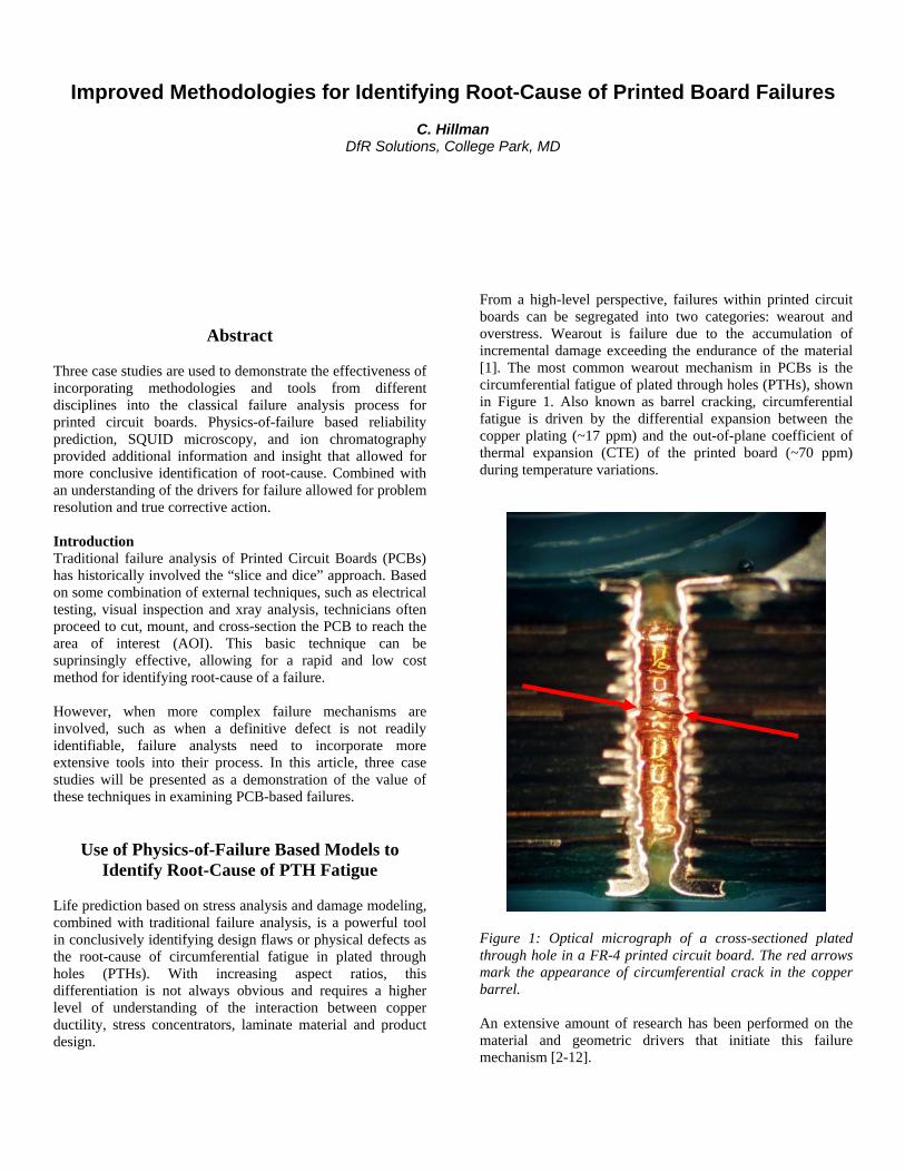
From a high-level perspective, failures within printed circuit boards can be segregated into two categories: wearout and overstress. Wearout is failure due to the accumulation of incremental damage exceeding the endurance of the material [1]. The most common wearout mechanism in PCBs is the circumferential fatigue of plated through holes (PTHs), shown in Figure 1. Also known as barrel cracking, circumferential fatigue is driven by the differential expansion between the copper plating (~17 ppm) and the out-of-plane coefficient of thermal expansion (CTE) of the printed board (~70 ppm) during temperature variations.
Figure 1: Optical micrograph of a cross-sectioned plated through hole in a FR-4 printed circuit board. The red arrows mark the appearance of circumferential crack in the copper barrel. An extensive amount of research has been performed on the material and geometric drivers that initiate this failure mechanism [2-12].
Manufacturing Defects in PTH Most occurrences of barrel cracking tend to be governed by the presence of manufacturing defects. This is primarily because the majority of electronic products are likely to be used in relatively benign environments, such as consumer, commercial, or industrial, where temperature fluctuations are controlled or minimized. In addition, the standard board thickness of 62 mil (1.57 mm) combined with a minimum PTH diameter of 15 mil (0.38 mm) creates a moderate aspect ratio of approximately 4:1, which will tend to be sufficiently robust in the most common application environments. The preponderance of manufacturing defects that lead to PTH cracking arises during the board fabrication process. These include etch pits (mouse bites), glass fiber protrusion, insufficient plating thickness, plating folds, and voiding. Etch pits are the result of etchant residues residing in the plated through hole barrel. The primary source of etchant residues are the chemicals used in the outer layer stripping process. Etchants can also be introduced if the bare board is reworked, such as stripping of the solderability coating. These etch pits can range in size from small ‘mouse bites’, shown in Figure 2, to complete removal of large sections of the PTH wall (seen in Figure 3). Etchants can also become trapped when vias are tented on only one side.
Figure 2 (120x): Optical micrograph of a cross-sectioned plated through hole in a FR-4 printed circuit board. The white arrows mark the appearance of etch pits, which resulted in circumferential crack propagation. Glass fiber protrusion into via walls also affects via plating thickness and hence can contribute to via cracking. Glass fiber protrusion may be due to process control variabilities during hole drilling, hole preparation or application of flash copper. Glass fiber protrusion is allowed by IPC guidelines for rigid copper boards only if the minimum copper plating thickness is met.
Figure 3 (120x): Dark field optical micrograph of PTH with suspected etch pit (marked by white arrow).
Figure 4 (120x): Optical micrograph of glass fiber bundle protrusion (marked with the white arrows). Insufficient plating thickness can lead to a reduction of mechanical and thermal properties and may lead to fatigue or overstress cracking. According to ANSI/IPC-A-600F [13], minimum acceptable average plating thickness for a Class 11 product is 20 microns, with isolated areas allowed to reach 15 microns in thickness. This specification is based on the minimum thickness that will reliably withstand multiple solder floats. The PTH shown in Figure 5 has an average plating thickness of approximately 18 microns with isolated areas reaching a thickness of 10 microns. Insufficient plating thickness is caused by either insufficient current/time in the copper plating bath or poor throwing
1 Class 1 is a general electronic product, such as consumer electronics and personal computers. Class 2 is a product where high performance and extended life is required, and for which uninterrupted service is desired, but is not critical. Class 3 are mission critical products, where failure can lead to extreme inconvenience, injury or loss of life.
power. Poor throwing power2 often provides uneven plating in the barrel, with thickness decreasing towards the center of the board. This is especially the case in high aspect ratio (greater than 4:1) PTHs, where it becomes necessary to use plating solutions operating under special conditions of low copper content, high sulphuric acid, low current density and low temperature. Since insufficient plating thickness was observed throughout the PTH, instead of just at the center of the board, the root-cause was determined to most likely be insufficient current or time in the copper plating bath.
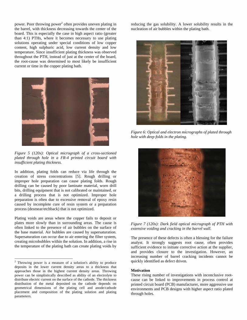
Figure 5 (120x): Optical micrograph of a cross-sectioned plated through hole in a FR-4 printed circuit board with insufficient plating thickness. In addition, plating folds can reduce via life through the creation of stress concentrations [5]. Rough drilling or improper hole preparation can cause plating folds. Rough drilling can be caused by poor laminate material, worn drill bits, drilling equipment that is not calibrated or maintained, or a drilling process that is not optimized. Improper hole preparation is often due to excessive removal of epoxy resin caused by incomplete cure of resin system or a preparation process (desmear/etchback) that is not optimized. Plating voids are areas where the copper fails to deposit or plates more slowly than in surrounding areas. The cause is often linked to the presence of air bubbles on the surface of the base material. Air bubbles are caused by supersaturation. Supersaturation can occur due to air entering the filter system, creating microbubbles within the solution. In addition, a rise in the temperature of the plating bath can create plating voids by
2 Throwing power is a measure of a solution's ability to produce deposits in the lower current density areas to a thickness that approaches those in the highest current density areas. Throwing power can be simplistically described as ability of an electrolyte to distribute electric current on the surface of the cathode. The thickness distribution of the metal deposited on the cathode depends on geometrical dimensions of the plating cell and anode/cathode placement and composition of the plating solution and plating parameters.
reducing the gas solubility. A lower solubility results in the nucleation of air bubbles within the plating bath.
Figure 6: Optical and electron micrographs of plated through hole with deep folds in the plating.
Figure 7 (120x): Dark field optical micrograph of PTH with extensive voiding and cracking in the barrel wall. The presence of these defects is often a blessing for the failure analyst. It strongly suggests root cause, often provides sufficient evidence to initiate corrective action at the supplier, and provides closure to the investigation. However, an increasing number of barrel cracking incidents cannot be quickly identified as defect driven. Motivation These rising number of investigations with inconclusive root-cause can be linked to improvements in process control at printed circuit board (PCB) manufacturer, more aggressive use environments and PCB designs with higher aspect ratio plated through holes.
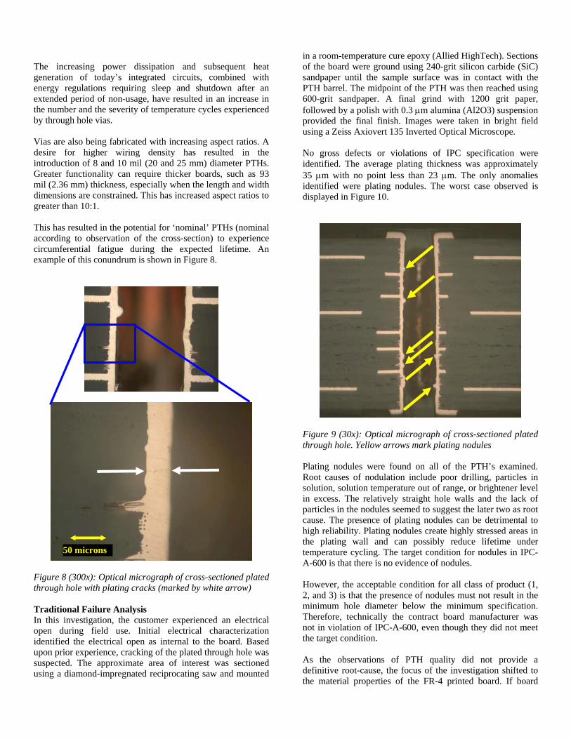
The increasing power dissipation and subsequent heat generation of today’s integrated circuits, combined with energy regulations requiring sleep and shutdown after an extended period of non-usage, have resulted in an increase in the number and the severity of temperature cycles experienced by through hole vias. Vias are also being fabricated with increasing aspect ratios. A desire for higher wiring density has resulted in the introduction of 8 and 10 mil (20 and 25 mm) diameter PTHs. Greater functionality can require thicker boards, such as 93 mil (2.36 mm) thickness, especially when the length and width dimensions are constrained. This has increased aspect ratios to greater than 10:1. This has resulted in the potential for ‘nominal’ PTHs (nominal according to observation of the cross-section) to experience circumferential fatigue during the expected lifetime. An example of this conundrum is shown in Figure 8.
Figure 8 (300x): Optical micrograph of cross-sectioned plated through hole with plating cracks (marked by white arrow) Traditional Failure Analysis In this investigation, the customer experienced an electrical open during field use. Initial electrical characterization identified the electrical open as internal to the board. Based upon prior experience, cracking of the plated through hole was suspected. The approximate area of interest was sectioned using a diamond-impregnated reciprocating saw and mounted
in a room-temperature cure epoxy (Allied HighTech). Sections of the board were ground using 240-grit silicon carbide (SiC) sandpaper until the sample surface was in contact with the PTH barrel. The midpoint of the PTH was then reached using 600-grit sandpaper. A final grind with 1200 grit paper, followed by a polish with 0.3 µm alumina (Al2O3) suspension provided the final finish. Images were taken in bright field using a Zeiss Axiovert 135 Inverted Optical Microscope. No gross defects or violations of IPC specification were identified. The average plating thickness was approximately 35 µm with no point less than 23 µm. The only anomalies identified were plating nodules. The worst case observed is displayed in Figure 10.
Figure 9 (30x): Optical micrograph of cross-sectioned plated through hole. Yellow arrows mark plating nodules Plating nodules were found on all of the PTH’s examined. Root causes of nodulation include poor drilling, particles in solution, solution temperature out of range, or brightener level in excess. The relatively straight hole walls and the lack of particles in the nodules seemed to suggest the later two as root cause. The presence of plating nodules can be detrimental to high reliability. Plating nodules create highly stressed areas in the plating wall and can possibly reduce lifetime under temperature cycling. The target condition for nodules in IPC-A-600 is that there is no evidence of nodules.
50 microns
However, the acceptable condition for all class of product (1, 2, and 3) is that the presence of nodules must not result in the minimum hole diameter below the minimum specification. Therefore, technically the contract board manufacturer was not in violation of IPC-A-600, even though they did not meet the target condition. As the observations of PTH quality did not provide a definitive root-cause, the focus of the investigation shifted to the material properties of the FR-4 printed board. If board
properties are not within expectations or if the board is not fully cured, this can create stresses sufficient to cause a nominal PTH to crack unexpectedly. The percent cure and material properties of the FR-4 laminate were measured using a differential scanning calorimeter (DSC)(Perkin Elmer Pyris-1) and a thermo mechanical analyzer (TMA)(Perkin Elmer TMA-7) A cyclic DSC test, consisting of ramping a sample of the board from room temperature to 200oC and back several times, showed no hysteresis behavior, suggesting that the board was fully cured. The results of TMA testing are displayed in Figure 10. The glass transition temperature, Tg, was found to be 155oC, above the original specification of 150oC. The out-of-plane coefficient of thermal expansion, CTE, of 70 ppm was well within the expected 60-90 ppm range of standard FR-4 printed boards.
Figure 10: Out-of-plane temperature-expansion curve of a FR-4 printed board subjected to thermo mechanical analysis Physics of Failure Based Modeling The lack of conclusive evidence from traditional failure analysis techniques required the use of a physics-of-failure (PoF) based approach. The PoF methodology emphasizes understanding the root-cause of failures by analyzing why, where, and how failures occur and using the obtained information to predict or prevent manifestation of potential failures in a product's operational lifecycle. In the case of PTH barrel fatigue, this involves the use of stress-strain analysis and damage models to predict the performance of the plated through hole during thermal cycling. The model used in this PoF-based analysis was based on work performed by Bhandarkar [5] and Yoder [6]. The model uses a one-dimensional elastic-plastic approximation to predict the stress and strain in the PTH barrel. The total deformation within the PTH barrel is described as
0
1
1
1L
AE
EAL
EAL
TLATE
PTHPTHm
j jj
j
j jj
j
m
jjj
PTHPTHPTH
+
∆+∆
=
∑
∑
∑
=
=
αα
δ
where α is the coefficient of thermal expansion, ∆T is the temperature range of the environment, E is the Young’s modulus, A is the effective area, L is the PCB layer thickness, and m is the total number of layers in the PCB. The non-linear thermomechanical behavior, and therefore the Young’s modulus, E, across the temperature range, is modeled by smaller linear segments, necessitating an iterative solution algorithim. The effective area, A, is chosen such that the stress results match linear finite element simulations. The resulting strain within the barrel wall is therefore
0Lδε =
where L0 is the total thickness of the PCB. The calculated strain range is then incorporated into a Coffin-Mason equation to predict time to failure,
( ) ( cff
bf
of NNE
222
ε )σσε+
−=
∆
where ∆ε is the strain range, σf is the fatigue strength coefficient, σo is the mean stress in the PTH plating, E is the modulus of the plating, Nf is the number of cycles to failure, b is the fatigue strength exponent, εf is the fatigue ductility coefficient, and c is the fatigue ductility exponent. A key aspect of the model is that manufacturing defects, such as those listed in the previous section, are not modelled explicitly, but are simulated through a plating quality factor. Therefore, the key question in determining if the failure was design or process related was to derive the quality factor from the test results and benchmark the quality factor against results in the literature. This would tell the customer if the performance of the plating, even if visually conforming, was below industry standards. The relevant geometric, material and test parameters, listed in Table 1, were inputted into the model. The resulting quality factor was determined to be 0.48. Existing data on thermal cycling of PTH was then pulled from the literature and a quality factor was calculated for each set of test results. The results are displayed in Table 2.
Table 1: List of inputs for the PTH fatigue model
Parameter Value PTH Spacing 20 mm PTH Hole Diameter 0.33 mm PTH Pad Diameter 0.65 mm Plating Thickness 0.035 mm Plating Modulus 120 GPa Plating CTE 17 ppm Board Thickness 2.03 mm Board Modulus (out of plane) 5.7 GPa Board CTE (out of plane) 70 ppm Temperature Cycles per Day 48 Maximum Temperature 105C Minimum Temperature -42C Time to Failure 324 cycles
Use of a quality factor allows for direct comparison between different accelerated life tests, even when the geometry or test parameters are dissimilar. Benchmarking the performance of the customer’s product to PTH fatigue behavior from the literature seems to show that the quality of the PTH was insufficent. If the quality factor was 0.75, an approximate average for the five data points in Table 2, the number of cycles to failure would have been expected to be closer to 900 cycles. This performance would have been well within the customer’s specification of 500 cycles to failure.
Table 2: Quality factors calculated from published test data
Reference [7]3 [7]4 [10] [11] [12]
Year 1988 1988 1997 2000 2002
Hole Diameter (mm) 0.25 0.33 0.35 0.30 0.34
Plating Thickness (µm) 20 32 25 30 25
Board Thickness (mm) 2.28 2.28 1.5 1.5 2.36
Out-of-Plane CTE (ppm) 70 83 63 50 N/A
Mean Time to First Failure (thermal cycles)
-35 to 125C 300 N/A N/A N/A N/A
-40 to 125C N/A N/A N/A N/A 750
-55 to 125C N/A N/A 925 2190 N/A
-65 to 125C N/A 371 N/A N/A N/A
Calculated Quality Factor 0.6 0.8 0.75 0.72 0.9
3 For a Class 3 product per IPC-A-600 4 For a ‘good’ vendor. In the round-robin study, vendors were rated superior, good, marginal and poor
Corrective Action As a result of using the PoF-based failure model, the early lifetime of the PTHs was determined to be a manufacturing issue, most likely due to insufficient plating ductility or yield strength. These plating values are impossible to quantify using traditional failure analysis, but can be indirectly assessed with the appropriate PoF-based tools. As a result of this investigation, it was recommended to the customer that minimum ductility and tensile strength requirements for plated copper be specified. Mechanical tests of plated copper can be based on IPC-TM-650 2.4.18.1, Tensile Strength and Elongation, In-House Plating. As a benchmark, IPC-TR-579 considers 30% to be a nominal ductility and 40,000 psi as a nominal tensile strength. An additional advantage of using the failure model approach was that the customer was able to quantify the effectiveness of potential corrective actions. Three corrective actions were proposed. The first was to reduce the board thickness. This redesign should result in minimal cost changes and have a minimal effect on other aspects of the design. The customer’s product is a ten-layer board. At a thickness of 2.03 mm, this results in an average laminate/prepreg thickness of approximately 185 microns. High technology boards are routinely fabricated with laminate/prepreg thicknesses of 100 microns. Reducing the average thickness to 150 microns (6 mil) would reduce the overall thickness of the board to approximately 1.81 mm. An alternative redesign was to specify thicker plating. As discussed previously, the plating thickness was 35 microns. A thicker plating, such as 50 microns, could be specified. The final potential action was a change in board material. The current board was a FR-4 epoxy with a measured out-of-plane CTE of approximately 70 ppm. Polyclad (PCL-FR-226 and PCL-FR-250) and Nelco (4000-6 and 4000-7) claim to manufacture laminate materials with low out-of-plane CTE, with Polyclad publishing a value of 50 ppm. The failure model was able to determine that at the current quality factor, the first two proposed changes would have individually resulted in an approximately 35% improvement in time to failure. These changes would not be sufficient to meet the 500 cycle test requirement. However, the failure model predicted that the use of low-expansion CTE board material would have resulted in a 900% increase in time to failure. Use of SQUID Microscopy to Identify Electrical
Leakage in Printed Circuit Boards While failures due to electrical opens can require innovative techniques to determine their root-cause, it is relatively unproblematic to locate the failure site through a series of electrical measurements. Electrical shorts are much more problematic. In addition to being more difficult to pinpoint because they can be located over a much wider area, their intermittent behavior can result in halting progress.
Superconducting Quantium Interferance Device (SQUID) microscopy is a radically new technique that uses detection of magnetic fields to image current paths within electronic devices. This technique has been successful in non-destructively identifying the location of low leakage currents, even when the failure site was between a power and ground plane (roughly equivalent to finding a needle in a haystack). The use of low voltage and low current is vastly superior to thermal imaging, which often results in irreplaceable damage to the failure site and masking of the true root cause of failure. In this case study, the customer was experiencing ignition of a 20-layer printed circuit board after approximately 1000 to 4000 operating hours in an indoor-controlled environment. High currents on the board resulted in extensive damage, effectively preventing initial identification of the failure site, failure mechanism, or root-cause. Failure Mechanism Identification A thorough approach to failure analysis, involving the identification of the failure mode, failure site, and failure mechanism, was used to isolate the root-cause of the ignition. The failure modes identified with burning are an electrical short or excessive heating. A listing of failure mechanisms that can initiate burning and charring within a printed circuit assembly is detailed in Table 3. All field failures originally occurred in fully-populated assemblies. While this implied that the original failure site could have been at the component level, accelerated tests on bare boards demonstrated shorting between power and ground. Assuming that the accelerated tests are triggering the same failure mechanisms seen in the field, the results suggested that the root-cause that was internal to the board and was not function of component failure. As seen in Table 3, this narrowed further examination to electrical overstress (EOS), electrochemical migration (ECM), and conductive filament formation (CFF) Electrical Overstress (Review) Electrical overstress (EOS) is a transfer of charge between two bodies that directly results in damage or failure. EOS can be the result of high voltage or high current. At the board level, high voltage can cause electric breakdown. High current can cause resistive heating that leads to a rapid increase in temperature. Electric Breakdown There are four possible failure mechanisms related to the initiation of an electrical arc across or through dielectric material: dust-buildup, air breakdown, surface flashover, and dielectric failure. The path of arc formation primarily differentiates the four failure mechanisms. Dust-buildup occurs when dust attracted by a direct current (DC) electric field spans adjacent conductors. The absorption of moisture by the dust over time can result in current leakage and eventually produce a short circuit.
Table 3: Failure mechanisms that have the potential to cause ignition on printed circuit assemblies.
IGNITION FAILURE MECHANISMS
Component Board/Assembly Electrical Overstress (EOS) - includes electrostatic damage (ESD) and excessive voltage or current.
Electrical Overstress (EOS)
Metallic Migration - migration between aluminum interconnects
Tin Whiskering (not applicable)
Wire Sweep - causes bond wire to contact, initiating electric short Dendritic Growth
Defective Heat Sink/Spreader Attachment - Cause the die to reach excessive temperatures
Conductive Filament Formation (CFF)
Capacitor Failure
Air breakdown is the condition in which an electrical arc spans the air gap between two conductors. During the operation of printed circuit boards, the values of air breakdown strength are often not used to when determining external conductor spacing. This is because electrical shorts between external conductors generally occur by surface flashover, at field stresses below the air breakdown strength. Surface flashover is electric breakdown along the surface of the printed circuit board between two conductors. Flashover initiates at the junction of the conductor (trace, pad, plated-through-hole (PTH)), insulator (laminate material), and gas (air or vacuum) and may or may not cause permanent damage. When the conduction path across the surface is established, degradation of the material can occur, reducing the lifetime of the insulative properties of the printed circuit board. The actual value of the electric field necessary for surface flashover can be highly variable and is dependent upon the smoothness and cleanliness of the board surface as well as other testing parameters. Published literature reports values ranging from 2 to 8 kV/mm. Dielectric failure is electric breakdown within a solid insulator between two conductors and is often concurrent with visible puncture and decomposition of the insulation material. All materials break down at some level of applied voltage gradient. This level can vary based upon material (thickness and quality of sample) and environmental (temperature and humidity) factors. The occurrence of dielectric failure is dependent upon the direction of the electrical arc. Dielectric strength and dielectric breakdown are the values of electrical field stress that result in dielectric failure. Dielectric strength is measured perpendicular to the lamination direction. The dielectric strength tends to be very high and is unlikely to be the dominant failure mechanism since the IPC-2221 provides for a relatively high safety factor (see Table 4). The electrical
field stress necessary for dielectric breakdown, which is measured parallel to the lamination direction, tends to be much lower because the fiber/resin interface provides a convenient path for electrical discharge. High Current/Resistive Heating Excessive current can lead to large temperature increases in metallic conductors. This process can lead to thermal runaway, since an increase in temperature will lead to an increase in resistance, which will lead to an even greater increase in temperature. High current can occur through shorts (low cross-sectional area translates to high resistance) or through the introduction of current surges in the power line. Electrical Overstress (Analysis) Because of the low voltage applied in the field, 3.3 VDC, dust-buildup, air breakdown, and surface flashover were considered unlikely failure mechanisms. Dielectric failure internal to the board is also considered unlikely. The board circuit was designed as per IPC-2221. As seen in Table 4, the interlayer and intralayer breakdown strength provide a sufficient safety factor above the maximum electric field stress recommended by industry specifications. Table 4: Comparison of measured dielectric strength and breakdown to the minimum electrical conductor spacings prescribed by IPC-2221, Table 6.1
B1 (Internal Conductors) Voltage (V) Conductor Spacing
(mm) Electrical Field Stress
(V/mm)
0-30 0.05 0-600
31-100 0.10 310-1000 Dielectric Strength [14]
(perpendicular to lamination) 44000
Dielectric Breakdown [14] (parallel to lamination) 1400
Resistive heating was a potential risk because of the high current, 30 amps, present in the board. According to IPC-2221, temperature rise, ∆T, for an internal trace is described as
ln (∆T) = 1.82 • [ln (I) + 4.20 – 0.74ln (A)] where I is the current and A is the cross-sectional area. Considering the possibility that a current of 30 amps was diverted to a 1 ounce signal trace, the resulting temperature rise would be
This temperature would be more than adequate to initiate burning and charring of the printed board. However, the time dependent behavior of the failure mode, between 1000 and 4000 hours of use, makes faulty design unlikely. Faulty design as a root-cause should initiate failure immediately unless the test coverage was insufficient and board complexity was such that certain circuits were only used sporadically during operation. In addition, the results of accelerated testing of bare boards indicated resistive heating was not likely to be the failure mechanism inducing ignition. The current applied during accelerated testing did not exceed 1 amp. The temperature rise in the signal trace due to 1 amp of current would be approximately 2oC, far below the temperature necessary to cause ignition. Dendritic Growth The process of dendritic growth requires moisture, ionic contaminants, and a voltage bias/electrical field. The source of ionic contaminants is varied and can include fluxes, solder paste residues, plating or etching solution deposits, poorly polymerized solder mask and improper handling procedures. Boards with dendritic growth will tend to exhibit sudden drops in resistance of large amplitude. In addition, if the contaminant level is high enough, dendritic growth can occur almost instantaneously. Both of these failure behaviors mimic the failure behavior seen on the failing boards. However, as with EOS, evidence acquired during accelerated testing and failure analysis suggested that dendritic growth was an unlikely root-cause. Bare boards that were thoroughly cleaned before accelerated testing experienced a significant decrease in resistance between power and ground planes. Removal of the layers 1 and 20, along with the corresponding solder masks, during failure analysis did not result in an increase in resistance between power and ground. Conductive Filament Formation (CFF) Multi-layer organic laminates used in printed wiring boards can develop an electrical short between two biased conductors due to the growth of conductive filaments. This phenomenon, called conductive filament formation (CFF), is an electrochemical process that involves the transport, usually ionically, of a metal through or across a nonmetallic medium under the influence of an applied electric field. The growth of metallic filaments is a function of temperature, humidity, voltage, laminate materials, manufacturing processes, and the geometry and spacing of the conductors. CFF usually involves higher electrical fields than ECM and does not involve metal redeposition at the cathode. There are two traditional paths for CFF: Delamination along the epoxy resin/glass fiber interface and Hollow Fibers. Delamination at the resin/fiber interface can be the result of defects in the manufacturing process , extensive temperature changes during operation, such as thermal cycling or thermal shock, humidity cycling or high humidity environments. Hollow fibers are caused by impurities in the glass melt. Hollow glass fibers
increase the opportunity for failure between close conductors because the capillary provides a convenient path for the formation of conductive filaments. CFF can also be accelerated due to copper wicking. Aggressive drilling can lead to excessive damage and delamination, allowing copper plating solution to wick into the interior of the printed board. This can reduce the spacing between conductors and hence the time necessary for CFF failure. Accelerated testing on bare boards resulted in drops in insulation resistance from tens of gigaohms to less than ten ohms over a period of 48 hours. This is not expected behavior for traditional conductive filament formation. The CALCE model [15] predicts a failure time of approximately 7500 hours for 5 mil PTH spacing at 50C/85%RH and 7.5 volts. When testing boards fabricated with Matshuita laminate, an automotive supplier did not measure insulation resistance in the megaohms until after 2000 hours at 85C/85%RH at 10 volts. Sun Microsystems did not experience insulation resistance in the megaohms until after 500 hours at 65C/85%RH at 100 volts [15]. CFF consists of path formation, dissolution and migration. Path formation tends to be the rate-limiting step. The rapid time to failure for the bare boards during accelerated testing suggested that path formation had already occurred. Based upon a methodical review of potential failure mechanisms, construction analysis, and accelerated testing, traditional failure mechanisms and root-causes did not seem to provide adequate explanation for the observed failure behavior. Failure Analysis Resolution required actual physical identification of a failure site. Unfortunately, this was hindered by the large area covered by the power and ground planes, which made identification of the failure site using functional or parametric testing virtually impossible. Visual inspection was also difficult due to the absence of a controlled burn area. The high glass transition temperature (Tg) of the dielectric material, 180oC, made it relatively resistant to high temperatures. The temperatures necessary to ignite the material were so high as to result in thermal runaway. The effect was binary: failed boards had either no visible charring or had large areas of the board severely burned, with any evidence of root-cause destroyed. Either case tended to hide the physical object causing the electrical short. This behavior also prevented use of thermal imaging, because the energy required to dissipate sufficient heat also tended to result in damage to the failure site. The initial solution was to modify a procedure used to identify very small voids that bridge multilayer ceramic capacitors (MLCCs) and cause current leakage. The resistance between a power and ground pin were monitored as the board was sectioned. Using a binary approach, the potential failure site was narrowed to a relatively small area. This area was very slowly ground and polished until a change in resistance was observed. At this
point, large angular particles were observed in the cross-section. There were two problems with this initial approach. First, considering the size of the board and the corresponding internal power and ground planes, the time required to find the short was time consuming. In addition, visual observation could not conclusively determine if these particles were the cause of the conductive path between power and ground, especially given the absence of a detectable conductive filament. More rapid and conclusive identification of the shorting path required the use of SQUID microscopy. SQUID Microscopy A Scanning SQUID Microscope is a sensitive near-field magnetic imaging system. This microscope can image buried current-carrying wires by measuring the magnetic fields produced by the currents, or it can be used to image fields produced by magnetic materials. By mapping the current in an integrated circuit or a package, short circuits can be localized and designs can be verified to ensure that charge is flowing where expected. The SQUID microscope used, Neocera MAGMA-C10, uses a high temperature SQUID with a sensitivity of 20 picotesla or two million times smaller than the Earth’s magnetic field. The microscope has been designed to keep a high temperature SQUID cooled below 80K and in vacuum while the device under test (DUT) is at room temperature and in air. The unique design of MAGMA-C10 also enables the SQUID to be positioned as close as 50 µm from the area of interest. Even though the SQUID is not in a magnetically shielded environment, the sensitivity is high enough to image currents as small as 600 nA at a 100 mm working distance with 30 ms averaging. The magnetic field produced by a sample can be imaged by rastering the sample in close proximity to the SQUID. If the sample contains a permanent magnetic field, as in many land grid arrays and lead frames, the microscope will map out this constant or “DC” magnetic field. In addition, electric currents in the device produce magnetic fields. The presence of a short circuit in an electrical part typically appears as a very strong concentration of magnetic field strength, with the field in opposite directions to either side of the short. During non-contact imaging of room temperature samples in air, the system achieves a raw, unprocessed spatial resolution equal to the distance separating the sensor from the current, or the effective size of the sensor (~30 microns for a standard SQUID tip), whichever is larger. To best locate a short in a buried layer, however, a Fast Fourier Transform (FFT) back-evolution technique can be used to transform the magnetic field image into an equivalent map of the current in an integrated circuit or printed circuit board. The resulting current map can then be compared to a circuit diagram to determine the fault location. With this post-processing of a magnetic image and the low noise present in SQUID images, it is possible to enhance the spatial resolution by factors of 5 or more over the near-field limited magnetic image. This enhanced resolution describes how well a scanning SQUID
microscope can resolve current paths in a sample. The system’s output is displayed as a false-color image of magnetic field strength or current density (after processing) versus position on the sample. The results from performing SQUID microscopy on a shorted board are displayed in Figure 11. The bright yellow area on the current map corresponds to the area of highest current density. This is representative of necking down of the conductor path, which is often a strong indication of an electrical short. Cross-sectioning of the board was performed at this location based upon the SQUID image.
Figure 11: Current map (left) and corresponding photograph (right) of an electrically shorted printed circuit board. The results of the cross-sectioning are displayed in Figure 12. A large, angular particle is observed bridging the dielectric between the power and ground planes. Tangential evidence, including mounding of copper at the power and ground planes and blackening of the surrounding dielectric material, strongly suggested that the particle was the cause of the drop in internal resistance. Definitive findings were provided through SQUID imaging of the cross-section
Figure 12 (500x): Particle identified between internal power and ground planes in the approximate area of electrical leakage.
The SQUID images are shown in Figure 13. The results clearly demonstrate that current is flowing through the particle, therefore verifying that the identified particle is the location of the short. However, bridging alone can not explain the electrical failure. This is because the angular nature of the particle suggests that it is electrically insulative. An additional mechanism, known as electrochemical migration (ECM), was most likely required.
Figure 13: Current map (left) and corresponding optical image (right) of the board cross-section shown in Figure 12. The red arrow identifies the particle sandwiched between layers 10 and 11. Electrochemical Migration Electrochemical Migration (ECM), also known as Metal Electromigration (MEM), Dendritic Growth, Conducting Filament Formation (CFF), and Conductive Anodic Filament (CAF) growth, is the redistribution of metal resulting from directed electrochemistry. Electrochemical migration on or in printed wiring boards (PWB’s) can result in electrical shorts that cause the circuit to fail. Traditional electrochemical migration involves four steps, path formation, electrodissolution, ion migration, and electrodeposition, and three requirements: ions (usually halides), water, and bias. For this failure mechanism, two path formations were speculated. The first possibility was the cracking of the particles, possibly during laminate manufacturing or board stackup. If such a crack were to occur, it would most likely run perpendicular to the pressing direction, providing an open path for filament migration to occur between layers 10 and 11. The second possibility was that the interfacial strength between particle and the epoxy matrix was poor, resulting in partial delamination during reflow, temperature cycling, or humidity cycling.
Layer 10 (power)
Layer 11 (ground) The minimum requirements for electrodissolution to occur are an electric field and a polar liquid such as water [17]. The magnitude of the electric field must be such that the anodic electromagnetic force (EMF) exceeds the standard electrode potential of the outermost anode material, which is 0.34 Volts for copper. In the presence of moisture, the following electrochemical reaction will occur in water adjacent to the anode:
2H20 → O2↑ + 4H + + 4e -
The increased concentration of H+ will reduce the pH of the water below 7.0, making the anode material susceptible to electrodissolution. In the case of copper, this can transpire as either
Cu → Cu + + e - or Cu → Cu ++ + 2e – If the electrolyte consists of water alone, Cu++ will be the predominant metallic ion. If the chloride ion Cl-, is present, the formation of the CuCl- ion will cause Cu+ to be the predominant metallic ion. Therefore, the presence of halides is not required to induce electrodissolution of copper. Ion Migration The electric field drives ionic migration. This causes the positive ions to travel along the field lines from the anode to the cathode through the ion transport path provided by the aqueous medium. The electrons to travel from the anode to the cathode through the ion transport path provided by the wiring to and through the biasing supply. Electrodeposition Once the ions reach the cathode, the following electrochemical reactions occur:
4H20 + 4e - → 2H2↑ + 4OH -
Cu + + e - → Cu or Cu ++ + 2e - → Cu Because cathodic electrodeposition is largely diffusion controlled, its rate depends on the metal ion concentration in the aqueous medium. The production of hydroxyl ions (OH-) at the cathode can reduce the rate of electrodeposition by combining metal ions with hydroxyl ions to form hydroxides. These hydroxides remove metal ions from the aqueous medium through partial precipitation. Thus the ECM rate is correlated with the solubility product of the metal ion hydroxide. Ionic contaminates, such as Cl -, can further change the ECM rate by forming alternate reaction paths and by forming additional ionic species, such as CuCl- in the case of copper and Cl-. Halides (Theory) Previous research has shown the presence of copper chloride salts during examination of suspected conductive filament formation (CFF) failures. X-ray dispersion studies on CFF performed by AT&T always showed copper affiliated with the conductive filaments and sometimes the presence of either sulfur or chlorine [18]. When investigating a potential CFF incident, IBM performed laser mass spectroscopy (LMS) on an area around a hollow glass fiber in FR-4 epoxy resin [19]. LMS detected positive sodium and copper ions and negative bromo-chlorinated copper ions. After performing a plasma etch to remove several molecular layers of material, LMS
identified positive potassium and copper ions and negative chlorine and copper chloride ions. Measurements using Energy Dispersive Spectroscopy (EDS) on suspected conductive filaments revealed that the material was primarily copper with either chlorine or bromine identified as the other major constituent. Electron diffraction studies performed on similar conductive filaments showed a microstructure comparable to 2CuCl2-5Cu(OH)2-H2O [20] As explained above, the presence of halides is not required for any of the steps involved in electrochemical migration (ECM). A classic example of this is migrated gold resistive shorts (MGRS). Researchers found that presence of chlorides led to the formation of dendritic filaments, but decreases in the insulation resistance still occurred when halides were absent. Halides can decrease the moisture threshold limit necessary for ECM to occur. This can lead to environments where ECM occurs only in the presence of halides, such as printed boards in controlled office conditions. If halides are present, they allow for a parallel chemical reaction to occur, which can accelerate the rate of ECM and therefore decrease the time to failure. Other studies have shown that the presence of non-halide materials, such as glycol, can also greatly accelerate the occurrence of ECM; however, like halides, glycol is primarily an accelerant and is not required for ECM to occur. Halides (Sources) Chloride can be present in small amounts in the glass fiber used to reinforce the epoxy matrix of the PCB. This is, because chloride is a common byproduct of the glass production method. The most common source of chlorides in PCBs is the etching process. Prevalent chemistries used in the etching process include alkaline ammonia, cupric chloride, peroxide-sulfuric acid, persulfates, and ferric chloride. Three of these, alkaline ammonia (ammonium chloride), cupric chloride, and ferric chloride, contain chloride ions, which can become absorbed or trapped in the printed circuit board. Persulfates are sometimes formulated with mercuric chloride, while peroxide-sulfuric acids are chloride-free. Other sources for chloride in the board fabrication processes include the cleaning and degreasing of laminates with hydrochloric acid and chlorinated solvents5, methylene chloride as a solvent in the liquid photoresist stripping process, hydrochloric acid as a neutralizer in the etch and resist process, sodium chlorite in the oxide bath, sodium hypochlorite in the potassium permanganate (electroless copper), palladium chlorides as a catalyst (electroless copper), salts from human contact, and cleaning with non-deionized water. Fluxes with chloride as an activator can also be a source. Most of the sources for bromide, including solder masks, marking inks, and fluxes that have a bromide as an activator material, are surface processes. The epoxy matrix
5 Rare due to concerns about chlorinated hydrocarbons (CHCs) effect on the ozone layer.
can also be a source for bromides from the flame retardant chemistry. IPC-TR-476A (reference) has stated that bromide in epoxy resin can diffuse to the surface, most likely during a high temperature process such as soldering. Halides (Measurements) While halides are not critical for ECM or CFF based failure mechanisms to initiate, the presence of halides will greatly accelerate the process and would be expected considering the rapid speed in which the failures occurred. There are currently two specifications for measuring halide content in printed wiring boards. The draft document, “IPC White Paper on Halogen-Free Materials Used for Printed Circuit Boards and Assemblies,” (reference) refers to ASTM-D-1847 (reference) as a test method to measure total halide content in epoxy resins. This test method was not used because the total concentration would include halides that were tightly bound to the epoxy matix. These immobile ions would not be expected to react with copper, forming the copper salts that lead to conductive filament formation. Instead, the extractable ion content was measured based upon test guidelines defined in MIL-STD-883, Method 5011 (reference). The first step is to ensure extreme cleanliness of the experimental setup. Extraction flasks were prepared by pouring 20 ml of nitric acid and an equal amount of deionized water, and agitating the solution. After agitation, the solution was allowed to stand for 15 minutes before the flasks were rinsed with deionized water ten times. The flasks were then fitted with condensers and refluxed for approximately 24 hours. The boiled water was discarded and the flasks were filled with fresh deionized water. The water was boiled for a few hours or until 2/3 of the water evaporates. Flasks were then allowed to air dry upside down. Before extraction, samples are prepared by cutting in 3 grams of measured dimensions to use in volume calculations. The length, height and thickness measured samples were added to 250 ml extraction flasks subjected to the cleaning process described above. 150 g ± 0.01 g of deionized water with a resistance of at least 18 megaohms was added to each flask. The prepared flask was refluxed for 60.0 hours ±1 hour. After allowing the solution to cool to room temperature, the extracts were analyzed by taking the extract solution and injecting it into the Dionex600 Ion Chromatograph injector port. The chromatograph was calibrated with 0.5 ppm, 1.0 ppm and 1.5 ppm chloride and bromide standard solutions. Three boards and two laminates were subjected to ion chromatography. One of the boards was was used as a reference sample. Specimens of similar volume were cut from each board. Special care was taken to ensure the saw was clean and was cooled and lubricated in deionized water. Powder-free gloves were used to handle the specimen. Solder mask was removed by grinding. Solder mask removal was necessary, because surface sources of contamination, such as from the solder mask, were not considered in this report. The
prepared samples were then washed in 18 megaohm water, again to prevent any surface contamination in the extraction flasks. For the three printed board samples, extract solutions were analyzed twice. For the bare laminates, extract solutions were analyzed once. The results for printed board samples are shown in Table 4. The ion concentrations in the extract can be converted to the extractable concentrations by multiplying by the deionized water volume at the end of refluxing (W) and dividing by the volume of the solid (V). Solid concentration = extract concentration x (W/V) As an example, the calculated volume for the sample cut from one board is 718 mm3. The measured concentration of chloride in the extract solution was 0.335 ppm. The volume of the extract solution was 108 ml. Therefore, the concentration of extractable chloride in this board is calculated as cCl = 0.335ppm × (0.108 liters ÷ 0.000718 liters) = 50.3 ppm The extractable chloride and bromide ion concentrations were calculated according to the above formula and are displayed in Table 5.
Table 5: Extractable chloride and bromide concentrations
Type Identifier Chloride Concentration
Bromide Concentration
1 50.3 ppm 222.1 ppm 2 17.2 ppm 163.4 ppm Board
Reference 10.9 ppm 17.1 ppm 1 0.6 ppm 0.0 ppm
Laminate 2 0.0 ppm 0.0 ppm
Discussion Epoxy resins can contain measurable levels of chlorine, such as sapponofiable, hydrolyzable and fixed chlorides. Additional halogens are added to laminates through glass sizes, wetting agents, curing agents and resin accelerators. The results from ion chromatography showed that there was very little extractable halide content in the base laminate. Instead, the source of halides found in printed boards was more likely from the board fabrication and assembly processes. Sources for chlorides in the board fabrication process were discussed previously. There are currently no specifications regarding the total amount of halides in printed boards and the total amount of extractable halides. In regards to environmental issues, both the United States and Japan are considering proposals that would limit chloride levels to 1200ppm and bromide levels to 900ppm. In regards to extractable levels, the only equivalent would be the experience of epoxy molding compounds (EMCs) in the electronic packaging industry. Before
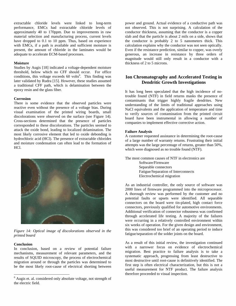
extractable chloride levels were linked to long-term performance, EMCs had extractable chloride levels of approximately 40 to 170ppm. Due to improvements in raw material selection and manufacturing process, current levels have dropped to 0.1 to 10 ppm. Thus, based on experience with EMCs, if a path is available and sufficient moisture is present, the amount of chloride in the laminates would be adequate to accelerate ECM-based processes. Moisture Studies by Augis [18] indicated a voltage-dependent moisture threshold, below which no CFF should occur. For office conditions, this voltage exceeds 60 volts6. This finding was later validated by Rudra [15]. However, these studies assumed a traditional CFF path, which is delamination between the epoxy resin and the glass fiber. Corrosion There is some evidence that the observed particles were reactive even without the presence of a voltage bias. During visual examination of the printed wiring boards, small discolorations were observed on the surface (see Figure 14). Cross-sections determined that the presence of particles corresponded to these discolorations. The particles seemed to attack the oxide bond, leading to localized delamination. The most likely corrosive element that led to oxide debonding is hydrochloric acid (HCl). The presence of extractable chlorides and moisture condensation can often lead to the formation of HCl.
Figure 14: Optical image of discolorations observed in the printed board Conclusion In conclusion, based on a review of potential failure mechanisms, measurement of relevant parameters, and the results of SQUID microscopy, the process of electrochemical migration around or through the particles was determined to be the most likely root-cause of electrical shorting between
6 Augis et. al. considered only absolute voltage, not strength of the electric field.
power and ground. Actual evidence of a conductive path was not observed. This is not surprising. A calculation of the conductor thickness, assuming that the conductor is a copper slab and that the particle is about 2 mils on a side, shows that the conductor is probably 2 to 5 nanometers thick. This calculation explains why the conductor was not seen optically. Even if the resistance prediction, similar to copper, was overly generous, an increase in resistance by three orders of magnitude would still only result in a conductor with a thickness of 2 to 5 microns. Ion Chromatography and Accelerated Testing in
Dendritic Growth Investigations It has long been speculated that the high incidence of no-trouble found (NTF) in field returns masks the presence of contaminants that trigger highly fragile dendrites. New understanding of the limits of traditional approaches using NaCl equivalents and the application of temperature and time to verify sources of contamination from the printed circuit board have been instrumental in allowing a number of companies to implement effective corrective action. Failure Analysis A customer requested assistance in determining the root-cause of a large number of warranty returns. Frustrating their initial attempts was the large percentage of returns, greater than 50%, which were diagnosed as no trouble found (NTF). The most common causes of NTF in electronics are Software/Firmware
Separable connectors Fatigue/Separation of Interconnects
Electrochemical migration As an industrial controller, the only source of software was 2000 lines of firmware programmed into the microprocessor. A thorough review was performed by the customer and no potential faults or upsets were identified. All separable connectors on the board were tin-plated, high contact force connectors, previously qualified for automotive environments. Additional verification of connector robustness was confirmed through accelerated life testing. A majority of the failures were occurring in a relatively controlled environment within six weeks of operation. For the given design and environment, this was considered too brief of an operating period to induce fatigue/separation of the solder joints on the board. As a result of this initial review, the investigation continued with a narrower focus on evidence of electrochemical migration. Best practice to failure analysis is to take a systematic approach, progressing from least destructive to most destructive until root-cause is definitively identified. The first step is often electrical characterization, but this is not a useful measurement for NTF product. The failure analysis therefore proceeded to visual inspection.
For a given design, and assuming a uniform distribution of contaminants, the primary driver for electrochemical migration (ECM), also known as dendritic growth, is the strength of the electric field between conductors. The visual inspection therefore focused on high voltage and fine pitch areas of the board. The results of visual inspection are displayed in Figure 15. Dendritic growth between solder pads on an insertion-mount microprocessor was observed using optical microscopy.
Figure 15: Optical micrograph of dendrite growth observed between two insertion mount pins While the failure mechanism was conclusively identified, corrective action cannot be implemented until the root-causes are identified. For ECM, this consists of identifying the source of contamination. Contamination can be introduced at any point in the manufacturing process. The most critical contamination is the presence of ionic residues, as these provide the electrolyte necessary for dendritic growth to occur. The most appropriate technique for identifying ionic residues is the use of ion chromatography. Ion Chromatography The chromatographic process can be defined as separation based upon the rate of movement through a medium. In the case of high performance liquid chromatography (HPLC), this involves passing the liquid, or mobile phase, through a column, or stationary phase, and tracking the adsorption and desorption behavior of the various phases or solutes within the liquid medium. Ion chromatography is a subset of HPLC, where the column material is selected for its resolve ionic molecules, such as anions, cations, or weak organic acids (WOAs) For contamination identification, the customer provided three boards from each of the seven steps of the manufacturing process: • Process Step 1 Bare PCB • Process Step 2 After through hole insertion /
before SMT
• Process Step 3 After SMT • Process Step 4 After hand insertion and wave • Process Step 5 Before conformal coating • Process Step 6 After conformal coating / before
stud insertion • Process Step 7 After final inspection
The procedure for measuring ionic residues was based upon IPC-TM-650, 2.3.28, Ionic Analysis of Circuit Boards (Ion Chromatography Method). Of paramount importance is to prevent the introduction of any additional ionic contaminants during the analysis process. In this regard, clean room vinyl gloves with less than 3 ppm of chloride are worn at all times and all chemical apparatus are cleaned with hi-purity deionized water (18 megaohm grade). Boards are placed into KAPAK heat sealable polyester film bags and immersed in an extraction solution of 75/25 isopropanol (IPA) and hi-purity deionized water. When preparing the extract solution, it is critical that the deionized water is ‘fresh’ (prepared within the past 48 hours), the IPA is high purity, and solution volume is large enough to cover the board. IPC TM-650 2.3.25.1 recommends 0.8 to 3 ml of extraction solution for each square cm of board surface area. The bags are heat sealed and placed in an 80ºC water bath for one hour. A small puncture in the bag is created as a pressure relief valve. The bags are removed from the water bath and the final volume of solution is recorded. Excessive loss of solution can lead to erroneous ion levels. Due to some initial analysis, the IC analysis focused on the detection of chloride (Cl-) and bromide (Br-). Chloride and bromide are part of the halide family, which are chemically active due to the arrangement of their electron shells. Chloride and bromide are considered two of the more important contaminants to detect because of their proclivity for reaction and their common use in industrial processes. As a result, several industrial and government specifications, detailed in Table 6, recommend maximum chloride and bromide contamination levels for printed circuit assemblies IC analysis is calibration sensitive, so the chromatograph was subjected to three-point calibration using 0.5 ppm, 1 ppm and 1.5 ppm standard solutions of chloride and bromide. After calibration, the extract solution from each board sample was injected into the column using a 1.8mM sodium carbonate/1.7mM sodium bicarbonate elluent. An example output is shown in Figure 16. The area under the peaks provides the concentration. The micrograms of ions per square inch of board area can then be calculated from the formula given below:
)(2
)(
)()(
22 inareasurfaceboard
mlextractofvolumemlgppmionconcentrat
inareagweight
×
×⎟⎠⎞⎜
⎝⎛ =
=
µµ
The presence of components is taken into consideration by adding an additional 10% to the total board surface area.
Table 6: Specifications for maximum contamination levels for finished assemblies
Source Bumiller [21]
Pauls [22]
GE [23]
NDCEE7 [24]
IPC8 [26]
DoD9 [27]
Chloride (µg/in2) 2 2 3.5 4.5 6.1 6.1
Bromide (µg/in2) 10 20 10 15 7.810 7.8
0.00 0.50 1.00 1.50 2.00 2.50 3.00 3.50 4.00-4.0
0.0
2.5
5.0
7.5
10.0
12.0 White Rogers #31 2P p-1-1 ECD_1µS
min
1 - Cl - 1.675
2 - Br - 3.042
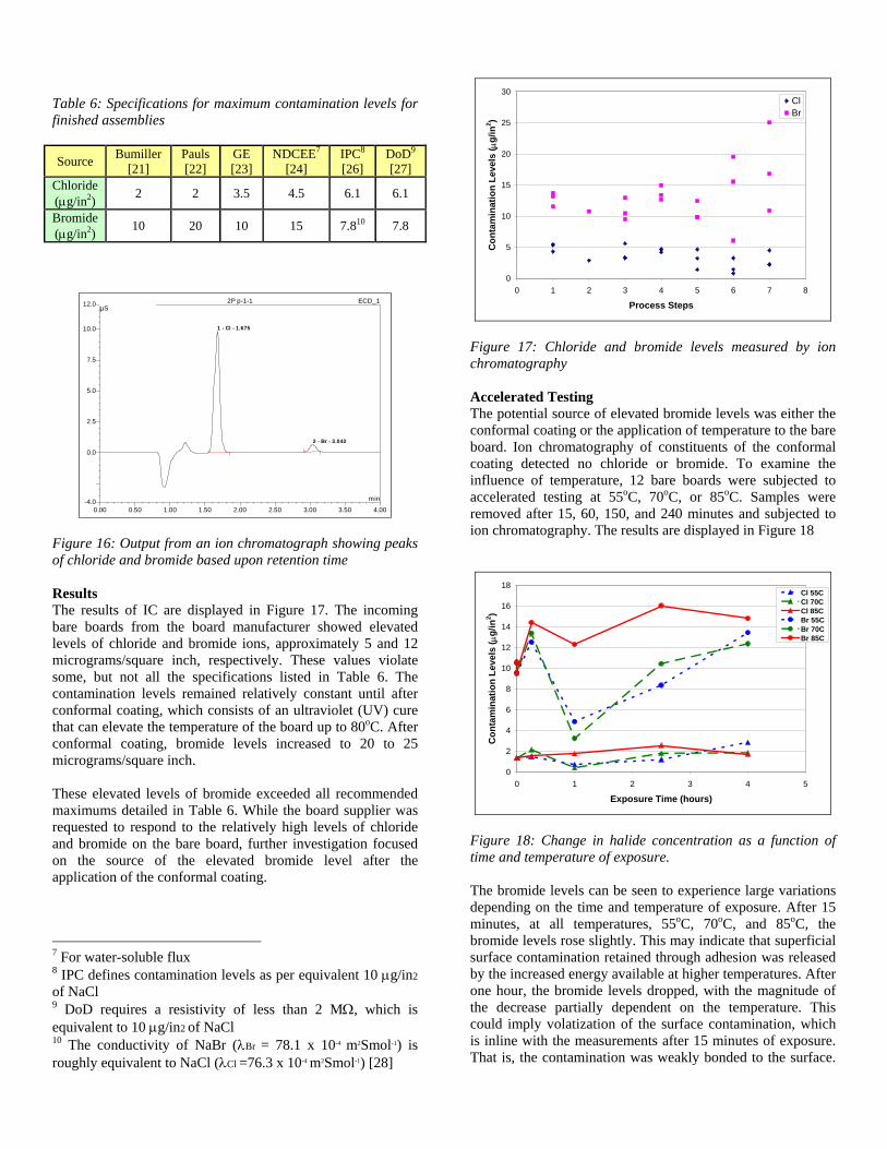
Figure 16: Output from an ion chromatograph showing peaks of chloride and bromide based upon retention time Results The results of IC are displayed in Figure 17. The incoming bare boards from the board manufacturer showed elevated levels of chloride and bromide ions, approximately 5 and 12 micrograms/square inch, respectively. These values violate some, but not all the specifications listed in Table 6. The contamination levels remained relatively constant until after conformal coating, which consists of an ultraviolet (UV) cure that can elevate the temperature of the board up to 80oC. After conformal coating, bromide levels increased to 20 to 25 micrograms/square inch. These elevated levels of bromide exceeded all recommended maximums detailed in Table 6. While the board supplier was requested to respond to the relatively high levels of chloride and bromide on the bare board, further investigation focused on the source of the elevated bromide level after the application of the conformal coating.
7 For water-soluble flux 8 IPC defines contamination levels as per equivalent 10 µg/in2
of NaCl 9 DoD requires a resistivity of less than 2 MΩ, which is equivalent to 10 µg/in2 of NaCl 10 The conductivity of NaBr (λBr = 78.1 x 10⁻⁴ m2Smol-1) is roughly equivalent to NaCl (λCl =76.3 x 10⁻⁴ m2Smol-1) [28]
0
5
10
15
20
25
30
0 1 2 3 4 5 6 7 8
Process Steps
Con
tam
inat
ion
Leve
ls ( µ
g/in
2 )
ClBr
Figure 17: Chloride and bromide levels measured by ion chromatography Accelerated Testing The potential source of elevated bromide levels was either the conformal coating or the application of temperature to the bare board. Ion chromatography of constituents of the conformal coating detected no chloride or bromide. To examine the influence of temperature, 12 bare boards were subjected to accelerated testing at 55oC, 70oC, or 85oC. Samples were removed after 15, 60, 150, and 240 minutes and subjected to ion chromatography. The results are displayed in Figure 18
0
2
4
6
8
10
12
14
16
18
0 1 2 3 4 5
Exposure Time (hours)
Con
tam
inat
ion
Leve
ls ( µ
g/in
2 )
Cl 55CCl 70CCl 85CBr 55CBr 70CBr 85C
Figure 18: Change in halide concentration as a function of time and temperature of exposure. The bromide levels can be seen to experience large variations depending on the time and temperature of exposure. After 15 minutes, at all temperatures, 55oC, 70oC, and 85oC, the bromide levels rose slightly. This may indicate that superficial surface contamination retained through adhesion was released by the increased energy available at higher temperatures. After one hour, the bromide levels dropped, with the magnitude of the decrease partially dependent on the temperature. This could imply volatization of the surface contamination, which is inline with the measurements after 15 minutes of exposure. That is, the contamination was weakly bonded to the surface.
Thus, initial exposure results in additional contamination being released, but additional times would result in loss of that weakly bonded contamination. After 2.5 and 4 hours bromine levels appear high again. There are two important findings from this behavior. First, it implies that a bromide-based contamination is likely diffusing to the surface, either from the solder mask or from the laminate. Second, it suggests that the elevated bromide levels seen in Figure 17 were due to contaminants present from the board manufacturer, rather than the introduction of contaminants during the conformal coating process. Corrective Action Often, the presentation of these findings is sufficient to initiate discussion with the supplier on the appropriate actions to remedy and remove these failure accelerators from future product. However, in this case, the supplier responded with their own ion chromatography results, claiming that sampling of bare boards at their facility resulted in bromide and chloride values well within industry specifications. The manufacturer of the printed boards reported levels of chloride and bromide as approximately 0.6 µg/in2, with testing performed as per IPC TM-650 2.3.28 (reference). However, when the actual measured PPM values were inputted into the formula described earlier, it was determined that the extraction volume was 45 ml for an 11.8 inch by 8.8 inch panel. This was considered insufficient to fully submerse the bare board, especially given the recommended extraction volume of 550 to 2000 ml of solution as per IPC TM-650 2.3.25.1 (reference). Using insufficient extraction volume most likely resulted in low levels of ions being detected. Once test approaches were unified and IC findings were correlated, it was determined that the printed board manufacturer had been using contaminated city water to wash the boards before the application of solder mask. This resulted in the trapping of bromide ions that diffused to the surface during the application of elevated temperatures, such as those seen in the conformal coating cure process.
Conclusion As displayed in the three case studies, standard methods and tools used in traditional root-cause analysis can result in incorrect or inconclusive findings when applied to failures in the current generation of printed circuit boards. The failure analyst must incorporate the latest techniques, especially in regards to the common failure mechanisms of PTH, CFF and ECM failure, to provide value to the client or customer. These techniques, in the realm of PoF modeling, current mapping, and contamination detection, are of worth because they are nonintuitive. That is, the provide information that is not detectable through simple physical characterization. Without a definitive determination of root-cause, corrective action can not be implemented and the prohibitive cost of warranty
returns and repair can be a detriment to the future viability of the customer.
References
1. S.B. Lee, A. Katz, and C. Hillman, Getting the Quality and Reliability Terminology Straight, IEEE CMPT-A, 21, 521-23 (1998)
2. A. Dasgupta and V. Rammppan, Simulation of the influence of manufacturing quality on the reliability of vias, Trans. ASME - J. Elec. Pack., 117, 141-146 (1995)
3. A. Ogumjimi, S. MacGregor, M. Pecht, and J. Evans, The effect of manufacturing and design process variabilities on the fatigue life of HDI vias, J. Electr. Manuf., 5, 11-119 (1995)
4. A. Prabhu, et. al., A thermo-mechanical fatigue analysis of HDI vias, Proc. INTERpack, 187-216 (1995)
5. S. Bhandarkar, et. al. Influence of selected design variables on thermomechanical stress distributions in plated through hole structures, Trans. ASME – J. Elec. Pack., 114, 8-13 (1992)
6. D. Yoder, S. Bhandarkar, and A. Dasgupta, Experimental and analytical investigation in aramid CCAs – Part 2, IPC Review, 20-27 (1993)
7. IPC Technical Report, Round robin reliability evaluation of small diameter plated through holes in printed wiring boards, IPC-TR-579 (1988)
8. V. Costa, E. Hernandez, F. Lechleiter, and M. Bremond, Electrical performances of MCM-D and MCM-SL HDI substrates for a high performance telecom application, Proc. Eur. Micro. Pack. Inter. Symp., 275-80 (2000)
9. D.C. Lai and G. Sure, Development and qualification of high complexity PCB, Proc. PanPac, 39-44 (2000)
10. D. Goyal, H. Azimi, K.P. Chong and M.J. Lii, Reliability of high aspect ratio plated through holes (PTH) for advanced printed circuit board (PCB) packages, Proc. IRPS, 129-35 (1997).
11. T. Kobayashi and S. Hayashida, A study on reliability modeling for through hole cracking failure in thermal enhanced PBGA laminate, Proc. ECTC, 1658-60 (2000)
12. J. Smetana, Plated through hole reliability with high temperature lead-free soldering, The Board Authority, 4, 50-64 (2002)
13. IPC Acceptability Standard, Acceptability of Printed Boards, IPC-A-600F (1999)
15. B. Rudra, M. Pecht and D. Jennings, Assessing time-to-failure due to conductive filament formation in multi-layer organic laminates, IEEE CPMT-B, 17, 269-276 (1994)
16. K. Sauter, Evaluating PWB design, manufacturing process, and laminate material impacts on CAF resistance; CircuiTree, 10-19 (2002)
17. G. Harsanyi and G. Inzelt, Comparing migratory resistive short formation abilities of conductor systems applied in advanced interconnection systems; Micro. Rel., 41, 229-237 (2001).
18. J. Augis, et. al., A humidity threshold for conductive anodic filaments in epoxy glass printed wiring boards, Proc. 3rd Inter. SAMPE Elec. Conf., 1023-1030 (1989)
19. Advanced Technology Workshop on Conductive Filament Formation in PWB’s and MCM-L; CALCE Electronic Packaging Research Center, University of Maryland, College Park, MD 20742; January 12 and 13, 1995.
20. W. Ready et. al., Microstructure of conductive anodic filaments formed during accelerated testing of printed wiring boards, Circuit World, 21, 5-10 (1995).
21. E. Bumiller, M. Pecht, and C. Hillman, The effect of electric field and chloride contamination on electrochemical migration, IEEE CPMT, submitted for publication
22. D. Pauls, Residues in printed wiring boards and assemblies, Circuit World, 27, 32-41 (2000)
23. Major Appliance Manufacturer, Printed circuit board assembly cleanliness specification, May 2003.
24. National Defense Center for Environmental Excellence (NDCEE), “Joint Test Protocol CC-P-1-1 for Validation of Alternatives to Lead-Containing Surface Finishes, for Development of Guidelines for Conformal Coating Usage, and for Qualification of Low-VOC Conformal Coatings,” Contract No. DAAA21-93-C-0046, Johnstown, PA, June 1999.
25. IPC, “Qualification and Performance Specification for Rigid Printed Boards,” IPC-6012A -AM, Section 3.10.1, Northbrook, IL, July 2000.
26. IPC, “Requirements for Soldered Electrical and Electronic Assemblies,” J-STD-001C, Section 8.36, Northbrook, IL, March 2000.
27. Department of Defense, “Circuit Card Assemblies, Rigid, Flexible, and Rigid Flex,” MIL-STD-28809B, Section 3.6.5.1, May 1988.
28. “Handbook of Chemistry and Physics – 80th edition”, CRC Press, New York, NY, 1999, pp. 5-94 & 5-95.
Important addresses
All manuscripts must be submitted to your paper mentor. Note that before submitting your paper, you must send the Copyright Transfer Form to: Jennifer Arnold ASM International 9639 Kinsman Road Materials Park, OH 44073 Tel: (440) 338-5151 ext. 5465 Fax: (440) 338-4634 E-mail: [email protected] Remember: The “readability” and overall quality of presentation of your research is in your hands. Please take care to prepare a high quality manuscript that will be an excellent contribution. Continue typing each subsequent page of your manuscript, up to the maximum pages, following the guidelines on this page.