Bo Qiao, ab Jiao Zhao,ab Jingli Liu,ab Binbin Yuanab and Xinyu Xuab
Lead sulfide (PbS) quantum dots (QDs) have been incorporated into PTB7:PC71BM BHJ active layers to
fabricate polymer solar cells (PSCs) and gather on the top surface of active layers to form an ultrathin
interlayer. The PbS QDs ultrathin interlayer with an appropriate thickness increases the carrier transport
capacity, exciton dissociation and reduces the carrier recombination, which leads to a higher short
circuit current (Jsc) and fill factor (FF). Finally, the power conversion efficiency (PCE) improves from
7.03% (control devices) to 7.87% with an ultrathin interlayer by doping 5% PbS QDs, while the current
density (Jsc) and fill factor (FF) enhances from 13.83 mA cm�2 to 14.81 mA cm�2 and from 68.70% to
70.85%, respectively.
Introduction
Polymer solar cells (PSCs) have advantages such as low-cost,light weight, exibility and easy fabrication via printing androll-to-roll coating technologies, and are being widely investi-gated as an alternative energy source.1–5 Although the powerconversion efficiency (PCE) of PSCs has reached 14% in the stateof the art,6 there is an urgent need to enhance the short-circuitcurrent density (Jsc),7 open-circuit voltage (Voc),8,9 ll factor (FF)10
and PCE for mass production and practical applications. Thereare many approaches to improve the performance of PSCs suchas developing new low bandgap donor materials,11,12 incorpo-ration of an additive into the active layer,13 tandem cellapproach14 and so on. In these PSCs, the charge transport ateach interface of different layers is critical for enhancing theefficiency, thus interfacial engineering plays an important roleto optimize the photovoltaic characteristics by increasing thecharge extraction and weakening the charge recombination.15
Methods of the interfacial modication in PSCs have been re-ported such as using different interlayers,16 polar solventdispose17 and so on. Alcohol-/water-soluble polymers are idealto be used as the interfacial layer in PSCs to avoid the dissolvingof two layers, which successfully improved device performance
Optical Information (Beijing Jiaotong
00044, China
jing Jiaotong University, Beijing 100044,
ing Abdulaziz University, Jeddah 21589,
rtment, Faculty of Electronic Engineering,
tion (ESI) available. See DOI:
as a dipole layer to increase the charge extraction.18 PFN is oneof alcohol-/water-soluble polymers and frequently be used asthe interfacial material in PSCs. The morphology of this poly-mer dipole layer is easy to be effected by the hydrophobicsurface of the previous layer. Thus, it's necessary to modify theinterface between the active layer and the polymer dipole layerby using an easy fabrication process, which could improve theelectron transfer from the active layer to the polymer dipolelayer and result in an optimized photovoltaic performance.
Quantum dots (QDs) materials have advantages such asa broad absorption range, high absorption coefficient, highconductivity and high carrier mobility.19–21 In addition, theconduction band and the valence band of QDs material can beadjusted via controlling its size for different application.Furthermore, QDs are dispersed and stabilized in solvent bythe introduction of ligands, which leads to the solutionprocess available.22 These characteristics make suitable QDsown the potential to enhance the performance of PSCs asadditives, or as the electron accepter. Lee23 et al. introducedPbS QDs with different bandgap energy (0.9–1.7 eV) instead of[6,6]-phenyl-C71-butyric-acid methyl-ester (PC71MB) as anelectron acceptor with poly[2,6-(4,40-bis(2-ethylhexyl)dithieno[3,2-b:20,30-d]silole)-alt-4,7(2,1,3-benzothiadiazole)] (PSBTBT)as the polymer donor, and got a PCE of 3.48%. Guo24 et al.reported a PCE of 6.94% by introducing the cadmium selenide(CdSe) QDs as an additive into the blend of poly [N-900-hepta-decanyl-2,7-carbazole-alt-5,5-(40,70-di-2-thienyl-20,10,30-ben-zothiadiazole)] (PCDTBT) and the fullerene derivative PC71BM.The improvements of the photovoltaic performance wereexplained by improving the charge transport property and tuningthe energy levels aer introducing the QDs. In addition to theseapplications, QDs could act as an interlayer to modify the interfaceof PSCs due to their adjusted energy levels to improve the
photovoltaic performance. However, there is no any such reportsaccording to out knowledge.
In this work, we achieved positive effects arising from theaddition of PbS QDs into the blend of poly[[4,8-bis[(2-ethyl-hexyl)oxy]benzo[1,2-b:4,5-b0]dithiophene-2,6-diyl][3-uoro-2-[(2-ethylhexyl)carbonyl]thieno[3,4-b]thiophenediyl]] (PTB7)and fullerene derivative [6,6]-phenyl-C71-butyric acid methylester (PC71BM). An ultrathin PbS QDs lm as an interlayerbetween the active layer and the polymer interfacial layer isformed to boost the transport of electrons by a new and easierexperiment process. The thickness and the morphology ofthe ultrathin PbS QDs lm were optimized with variousweight ratios (wt). Then the carrier transport capacity and theexciton dissociation was investigated. The results show thatJsc and FF, then the photovoltaic performance of preparedPTB7:PC71BM photovoltaics devices are enhanced.
Experimental
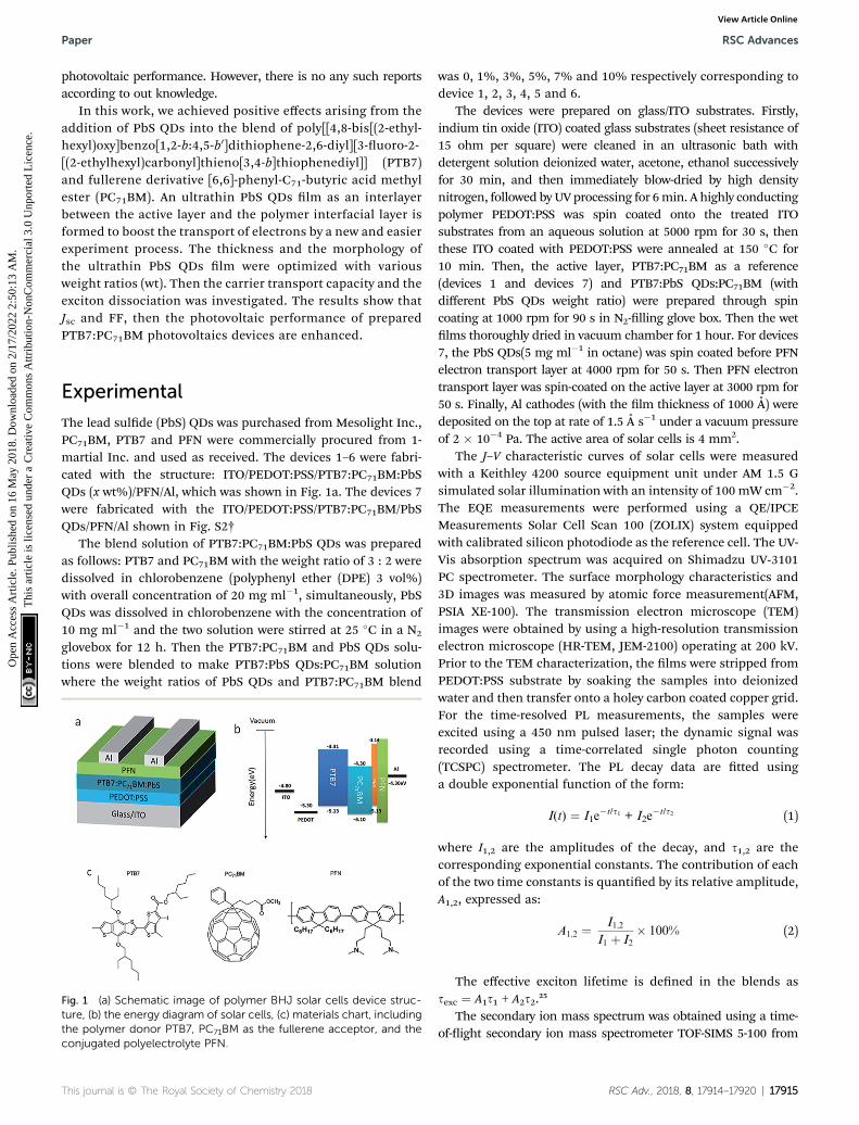
The lead sulde (PbS) QDs was purchased from Mesolight Inc.,PC71BM, PTB7 and PFN were commercially procured from 1-martial Inc. and used as received. The devices 1–6 were fabri-cated with the structure: ITO/PEDOT:PSS/PTB7:PC71BM:PbSQDs (x wt%)/PFN/Al, which was shown in Fig. 1a. The devices 7were fabricated with the ITO/PEDOT:PSS/PTB7:PC71BM/PbSQDs/PFN/Al shown in Fig. S2†
The blend solution of PTB7:PC71BM:PbS QDs was preparedas follows: PTB7 and PC71BM with the weight ratio of 3 : 2 weredissolved in chlorobenzene (polyphenyl ether (DPE) 3 vol%)with overall concentration of 20 mg ml�1, simultaneously, PbSQDs was dissolved in chlorobenzene with the concentration of10 mg ml�1 and the two solution were stirred at 25 �C in a N2
glovebox for 12 h. Then the PTB7:PC71BM and PbS QDs solu-tions were blended to make PTB7:PbS QDs:PC71BM solutionwhere the weight ratios of PbS QDs and PTB7:PC71BM blend
Fig. 1 (a) Schematic image of polymer BHJ solar cells device struc-ture, (b) the energy diagram of solar cells, (c) materials chart, includingthe polymer donor PTB7, PC71BM as the fullerene acceptor, and theconjugated polyelectrolyte PFN.
was 0, 1%, 3%, 5%, 7% and 10% respectively corresponding todevice 1, 2, 3, 4, 5 and 6.
The devices were prepared on glass/ITO substrates. Firstly,indium tin oxide (ITO) coated glass substrates (sheet resistance of15 ohm per square) were cleaned in an ultrasonic bath withdetergent solution deionized water, acetone, ethanol successivelyfor 30 min, and then immediately blow-dried by high densitynitrogen, followed by UV processing for 6min. A highly conductingpolymer PEDOT:PSS was spin coated onto the treated ITOsubstrates from an aqueous solution at 5000 rpm for 30 s, thenthese ITO coated with PEDOT:PSS were annealed at 150 �C for10 min. Then, the active layer, PTB7:PC71BM as a reference(devices 1 and devices 7) and PTB7:PbS QDs:PC71BM (withdifferent PbS QDs weight ratio) were prepared through spincoating at 1000 rpm for 90 s in N2-lling glove box. Then the wetlms thoroughly dried in vacuum chamber for 1 hour. For devices7, the PbS QDs(5 mg ml�1 in octane) was spin coated before PFNelectron transport layer at 4000 rpm for 50 s. Then PFN electrontransport layer was spin-coated on the active layer at 3000 rpm for50 s. Finally, Al cathodes (with the lm thickness of 1000 A) weredeposited on the top at rate of 1.5 A s�1 under a vacuum pressureof 2 � 10�4 Pa. The active area of solar cells is 4 mm2.
The J–V characteristic curves of solar cells were measuredwith a Keithley 4200 source equipment unit under AM 1.5 Gsimulated solar illumination with an intensity of 100 mW cm�2.The EQE measurements were performed using a QE/IPCEMeasurements Solar Cell Scan 100 (ZOLIX) system equippedwith calibrated silicon photodiode as the reference cell. The UV-Vis absorption spectrum was acquired on Shimadzu UV-3101PC spectrometer. The surface morphology characteristics and3D images was measured by atomic force measurement(AFM,PSIA XE-100). The transmission electron microscope (TEM)images were obtained by using a high-resolution transmissionelectron microscope (HR-TEM, JEM-2100) operating at 200 kV.Prior to the TEM characterization, the lms were stripped fromPEDOT:PSS substrate by soaking the samples into deionizedwater and then transfer onto a holey carbon coated copper grid.For the time-resolved PL measurements, the samples wereexcited using a 450 nm pulsed laser; the dynamic signal wasrecorded using a time-correlated single photon counting(TCSPC) spectrometer. The PL decay data are tted usinga double exponential function of the form:
I(t) ¼ I1e�t/s1 + I2e
�t/s2 (1)
where I1,2 are the amplitudes of the decay, and s1,2 are thecorresponding exponential constants. The contribution of eachof the two time constants is quantied by its relative amplitude,A1,2, expressed as:
A1;2 ¼ I1;2
I1 þ I2� 100% (2)
The effective exciton lifetime is dened in the blends assexc ¼ A1s1 + A2s2.25
The secondary ion mass spectrum was obtained using a time-of-ight secondary ion mass spectrometer TOF-SIMS 5-100 from
ION-TOF GmbH (Munster, Germany). For all of the depth prolemeasurements, a gas cluster ion gunO2
+ operating at a 1 keV beamvoltage with a 45� incident angle was used for sputter erosion, andthe sputtering rate was 0.263 nm s�1 for SiO2. Analysis was per-formed using a Bi1
+ liquid metal ion gun operated at 30 keV beamvoltage with a 45� incident angle over a 100 mm� 100 mm2 regionin the center of the eroded area. A low energy electron ood gunwas carried out for charge compensation.
Results and discussion
The device structure and the highest occupied molecular orbital(HOMO), lowest unoccupied molecular orbital (LUMO), valenceband and conduction band of component materials used indevices are shown in Fig. 1a and b, respectively. The energyband diagram of PbS QDs was measured by ultraviolet photo-electron spectroscopy(UPS).26 The molecular structures of theorganic polymer donor PTB7, fullerene acceptor PC71BM thatused as the photoactive layer and water/alcohol soluble conju-gated polymer poly[(9,9-bis(30-(N,N-dimethylamino)-propyl)-2,7-uorene)-alt-2,7-(9,9-dioctyluorene)] PFN that used as theinterlayer material are shown in Fig. 1c.
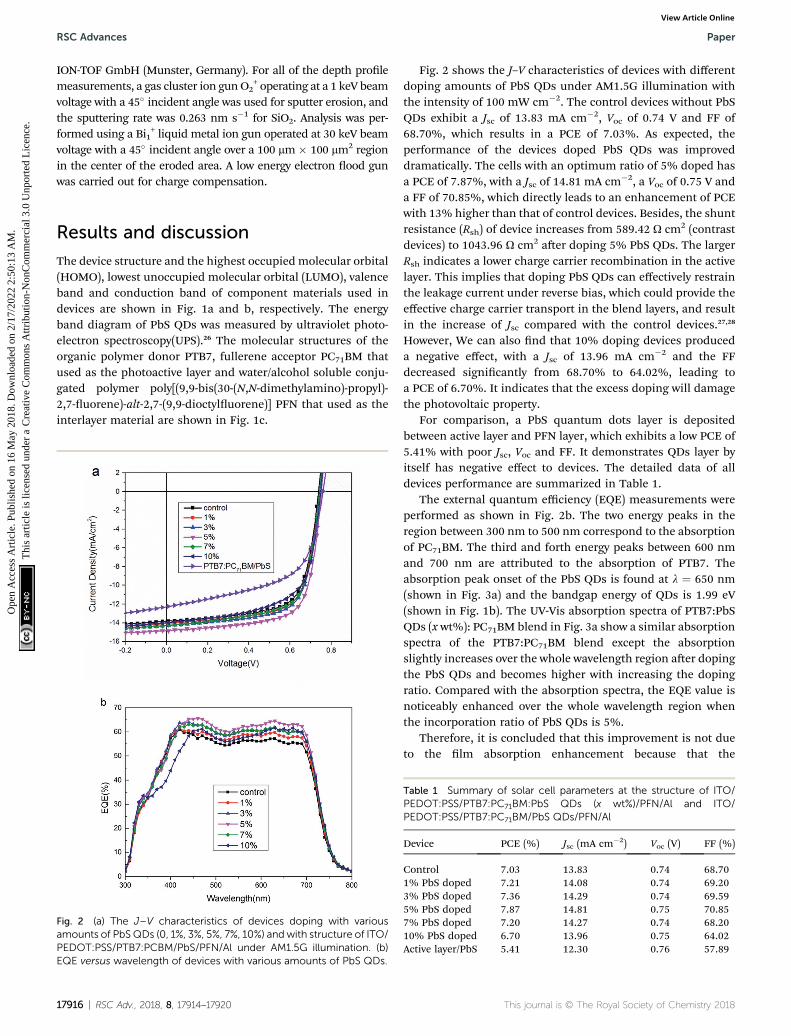
Fig. 2 (a) The J–V characteristics of devices doping with variousamounts of PbSQDs (0, 1%, 3%, 5%, 7%, 10%) andwith structure of ITO/PEDOT:PSS/PTB7:PCBM/PbS/PFN/Al under AM1.5G illumination. (b)EQE versus wavelength of devices with various amounts of PbS QDs.
17916 | RSC Adv., 2018, 8, 17914–17920
Fig. 2 shows the J–V characteristics of devices with differentdoping amounts of PbS QDs under AM1.5G illumination withthe intensity of 100 mW cm�2. The control devices without PbSQDs exhibit a Jsc of 13.83 mA cm�2, Voc of 0.74 V and FF of68.70%, which results in a PCE of 7.03%. As expected, theperformance of the devices doped PbS QDs was improveddramatically. The cells with an optimum ratio of 5% doped hasa PCE of 7.87%, with a Jsc of 14.81 mA cm�2, a Voc of 0.75 V anda FF of 70.85%, which directly leads to an enhancement of PCEwith 13% higher than that of control devices. Besides, the shuntresistance (Rsh) of device increases from 589.42 U cm2 (contrastdevices) to 1043.96 U cm2 aer doping 5% PbS QDs. The largerRsh indicates a lower charge carrier recombination in the activelayer. This implies that doping PbS QDs can effectively restrainthe leakage current under reverse bias, which could provide theeffective charge carrier transport in the blend layers, and resultin the increase of Jsc compared with the control devices.27,28
However, We can also nd that 10% doping devices produceda negative effect, with a Jsc of 13.96 mA cm�2 and the FFdecreased signicantly from 68.70% to 64.02%, leading toa PCE of 6.70%. It indicates that the excess doping will damagethe photovoltaic property.
For comparison, a PbS quantum dots layer is depositedbetween active layer and PFN layer, which exhibits a low PCE of5.41% with poor Jsc, Voc and FF. It demonstrates QDs layer byitself has negative effect to devices. The detailed data of alldevices performance are summarized in Table 1.
The external quantum efficiency (EQE) measurements wereperformed as shown in Fig. 2b. The two energy peaks in theregion between 300 nm to 500 nm correspond to the absorptionof PC71BM. The third and forth energy peaks between 600 nmand 700 nm are attributed to the absorption of PTB7. Theabsorption peak onset of the PbS QDs is found at l ¼ 650 nm(shown in Fig. 3a) and the bandgap energy of QDs is 1.99 eV(shown in Fig. 1b). The UV-Vis absorption spectra of PTB7:PbSQDs (x wt%): PC71BM blend in Fig. 3a show a similar absorptionspectra of the PTB7:PC71BM blend except the absorptionslightly increases over the whole wavelength region aer dopingthe PbS QDs and becomes higher with increasing the dopingratio. Compared with the absorption spectra, the EQE value isnoticeably enhanced over the whole wavelength region whenthe incorporation ratio of PbS QDs is 5%.
Therefore, it is concluded that this improvement is not dueto the lm absorption enhancement because that the
Table 1 Summary of solar cell parameters at the structure of ITO/PEDOT:PSS/PTB7:PC71BM:PbS QDs (x wt%)/PFN/Al and ITO/PEDOT:PSS/PTB7:PC71BM/PbS QDs/PFN/Al
Fig. 3 (a) UV-Vis absorption spectra of PbS QDs, PC71BM, PTB7 andPTB7: PC71BM blend film various amounts of PbS QDs doped, (b) theJ–V characteristics of devices doping without and with 5 wt% PbS QDsover wavelength below 450 nm (symbols) and the whole region (lineand symbols).
Fig. 4 ToF-SIMS depth profile for: (a) Pb2+ in film doping with differentamounts of PbS QDs within 5 nm, (b) Pb2+, C+ and O2� in whole filmwith 5% PbS QDs. The inset figure is an amplification of local curves ofthe film with 1%, 3%, 5% PbS QDs doped. The top horizontal axisrespect the reference thickness at sputter rate is 0.263 nm s�1 for SiO2.(c) Structure of devices with doping 5% PbS QDs.
Paper RSC Advances
Ope
n A
cces
s A
rtic
le. P
ublis
hed
on 1
6 M
ay 2
018.
Dow
nloa
ded
on 2
/17/
2022
2:5
0:13
AM
. T
his
artic
le is
lice
nsed
und
er a
Cre
ativ
e C
omm
ons
Attr
ibut
ion-
Non
Com
mer
cial
3.0
Unp
orte
d L
icen
ce.
View Article Online
absorption spectrum (shown as Fig. 3a) is not sensitive to theincrease ratio of PbS QDs. It means that PbS QDs doping doesnot help to formmore excitons but help to dissociate excitons ortransport charges.
In order to investigate the physical mechanism of PbS QDs indevices, we measured J–V characteristics of devices without andwith 5% PbS QDs under the illumination of a monochromaticlight at 450 nm, which is shown in Fig. 3b. According to the UV-Vis absorption spectra of PbS QDs and PTB7, it's obvious thatthe absorption intensity of PTB7 is weak below 450 nm whilePbS QDs has strong absorbance. However, the J–V curves arealmost same for two devices under 450 nm illumination. It alsoindicate that the photons absorbed by PbS QDs can not betransferred to free carriers, and there is not Forster energytransfer between PbS QDs to PTB7.
In other words, the light absorbed by PbS QDs does notcontribute to the enhancement of PCE.
The location and distribution of PbS QDs in the active layeris very important to play its role to enhance the whole deviceperformance. Time of Flight Secondary Ion Mass Spectrometry(ToF-SIMS) was utilized to gure out the distribution of PbS QDsand PTB7 by measuring the yield of lead ion and uorine (Pb2+
and C+). The ToF-SIMS results in the vertical direction of lmswith different amounts of PbS QDs are shown in Fig. 4. InFig. 4a, the intensity of Pb2+ in the lm surface corresponding to
the beginning of the sputter time enhances with the increasingdoping amounts of PbS QDs till the doping over 5%, whichindicates that PbS QDs cover the surface of lm completelywhen the doping amounts is 5% and 7%, and covers partiallywhen it's 1% and 3%. Furthermore, the intensity of Pb2+ in lmswith lower doping than 5% reaches zero rapidly in less than 2seconds (which is clearly shown in the inset gure) while the
decreasing rate of intensity is much slower with doping 7% PbSQDs. This phenomenon proves that during the lm formation,PbS QDs prefer to move upward to form an ultrathin layer in thesurface. When the surface of the lms is overspreaded by PbSQDs, partial PbS QDs migrate or diffuse into the inside of BHJlms. Therefore, the thickness of PbS QDs layer with 7% dopedis larger than that of the layer doped with 5%. To related withthe photovoltaic performance of different devices, we can makea reasonable conclusion that the ultrathin PbS QDs layer couldpromote the carrier transport or charge extraction, yet a thickPbS QDs layer has an adverse effect to organic solar cells.
To conrm that PbS QDs gathers on the top of lms,29,30 yieldof lead ion, carbon ion and oxygen ion were measured respec-tively in the whole lm with doping 5% PbS QDs as shown inFig. 4b. Pb2+ represents PbS QDs, C is the fragment elementassociated with PTB7 molecule, and O2� is main associatedwith ITO (due to its little content in PTB7). At the beginning, inwhich it corresponds to the surface of the BHJ layer, the yieldintensity of Pb2+ is more than other two ions. Aer 2 second andtill 148 second, the intensity of Pb2+ is almost zero. It indicatesPbS QDs locating on the top surface, and there is not PbS QDsexisting inside the BHJ layer. Aer the yield intensity of O2�
rapidly rises to show the bottom of the active layer and thesurface of ITO arrived. Then a very little Pb2+ still was detectedin the bottom of the lm and could be neglected compared withthe surface Pb2+ yield. According to above results, PbS QDsgather on the top of the active layer, we conjecture that PbS QDswould oat upward during spinning progress due to the lessmolar mass of PbS QDs than that of PTB7 and PC71BM. It hasa new structure of device with 5% doping PbS QDs, shown inFig. 4c, which could get the maximum improvement of deviceperformance.
The morphology of this PbS QDs layer are presented bytapping-mode atomic force microscopy (AFM) images (surfacearea: 5 � 5 mm2) of lms with 0, 5%, and 10% PbS QDs in Fig. 5.As we can see, the blend lms don't exhibit apparent variationupon doping 5% PbS QDs (Fig. 5b and e) and 10% PbS QDs(Fig. 5c and f). The blend lm with 5% PbS QDs doped showsa rather smooth surface morphology with root mean square(RMS) values of about 1.195 nm. In contrast, the blend lm
Fig. 5 AFM image of PTB7:PC71BM blend film (a and d) without PbSQDs, (b and e) doping with 5% QDs, (c and f) doping with 10% QDs.
17918 | RSC Adv., 2018, 8, 17914–17920
without PbS QDs doped (Fig. 5a) and with 10% PbS QDs doped(Fig. 5c) show rough morphology with RMS values of about1.381 nm and 1.509 nm respectively, which is similar with theFF of devices. The rather smooth surface is conducive to theinterface contact between layers and reduces the interfaceresistance to promote the charge transport and extraction.
It also can be proved by transmission electron microscopy(shown in Fig. S1†). The black domain is assigned as thePC71BM aggregation because its ordered aggregation showsrelatively higher electron scattering density compared to theamorphous polymer aggregation.31 The blend lm with 5% PbSQDs doped exhibits rather compact bulk morphology whichindicates the PC71BM aggregation decreases and homogeneousdispersion throughout the lm. It is benet to form betterinterpenetrating network structure in the bulk to promote thecharge transport.
These phenomena indicate that PbS QDs ultrathin layer withappropriate thickness are favorable to charge transport andextraction in the active layer, to improve the photovoltaicperformance.
The dark J–V characteristics of electron-only devices weremeasured with the structure of ITO/active layer/PFN/Al shownin Fig. 6. Jsc of doped devices with lower contents in Fig. 6 islarger than that of control device it means that PbS QDs ultra-thin layer is benet to enhance the electron transport property.As the same time, a largest Jsc was detected in the device withthe doping amount of 5%, which is consistent with thetendency of the photocurrent curves in Fig. 2. It implies that anultrathin QDs layer formed by doping 5% QDs is maximallybenet to charge transport. Then we made a realistic evaluationon the apparent charge carrier mobility of blend lms throughthe spare charge limit current (SCLC) method.18,25,32,33 Accordingto the Mott–Gurney law, current density is given by (eqn (3))
J ¼ 9303rmV2/8L3 (3)
where J is the current density, 30 is the permittivity of free space,3r is the relative dielectric constant of the BHJ layer, m is thecharge carrier mobility, L is the thickness of the BHJ layer, and Vis the voltage drop across the device.34 The computed results
Fig. 6 Dark J–V characteristics of electron-only devices with variousamounts of PbS QDs doping (1%, 3%, 5%, 7%, 10%), for the calculationof electron mobility using the Mott–Gurney equation.
show that the electron-mobility me increases from 9.58 � 10�5
cm2 V�1 s�1 to 6.90 � 10�4 cm2 V�1 s�1 with an ultrathin QDslayer formed by doping 5% QDs. That is to say, upon the PbSQDs ultrathin layer, the electron mobility increase 7.2 times.Those are direct evidence that charge transport capacity islargely enhanced by PbS QDs ultrathin layer and contributes toimprovement of Jsc, FF as well as the performance of the solarcells.
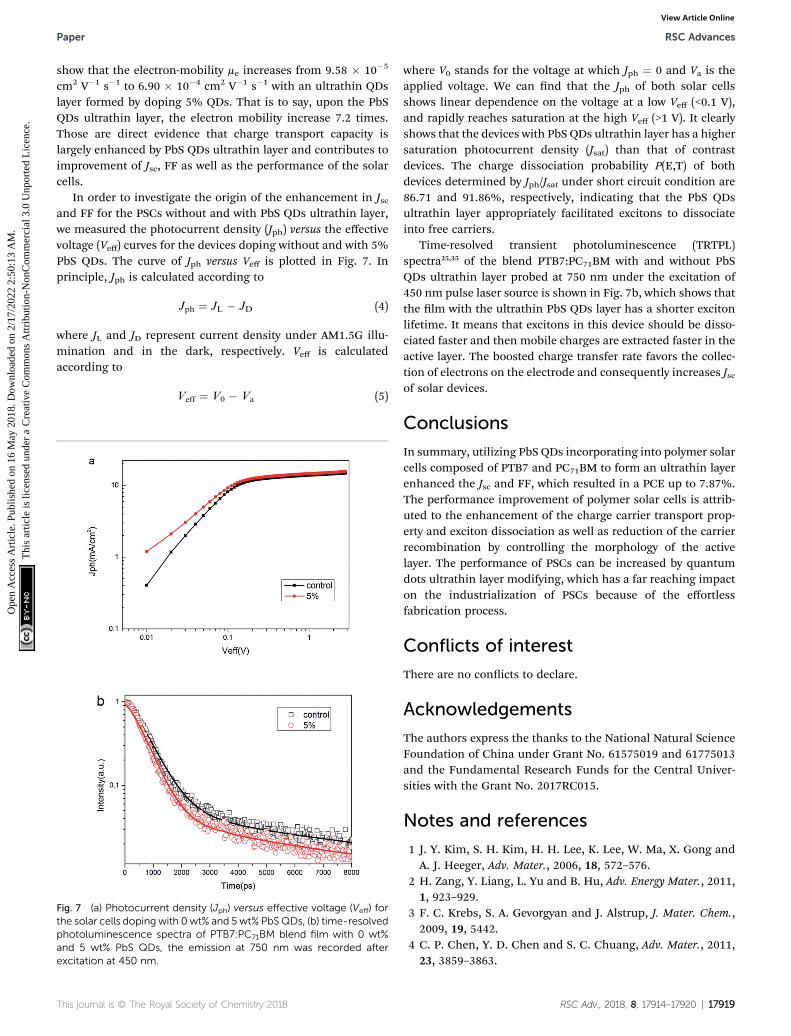
In order to investigate the origin of the enhancement in Jscand FF for the PSCs without and with PbS QDs ultrathin layer,we measured the photocurrent density (Jph) versus the effectivevoltage (Veff) curves for the devices doping without and with 5%PbS QDs. The curve of Jph versus Veff is plotted in Fig. 7. Inprinciple, Jph is calculated according to
Jph ¼ JL � JD (4)
where JL and JD represent current density under AM1.5G illu-mination and in the dark, respectively. Veff is calculatedaccording to
Veff ¼ V0 � Va (5)
Fig. 7 (a) Photocurrent density (Jph) versus effective voltage (Veff) forthe solar cells doping with 0wt% and 5wt% PbSQDs, (b) time-resolvedphotoluminescence spectra of PTB7:PC71BM blend film with 0 wt%and 5 wt% PbS QDs, the emission at 750 nm was recorded afterexcitation at 450 nm.
where V0 stands for the voltage at which Jph ¼ 0 and Va is theapplied voltage. We can nd that the Jph of both solar cellsshows linear dependence on the voltage at a low Veff (<0.1 V),and rapidly reaches saturation at the high Veff (>1 V). It clearlyshows that the devices with PbS QDs ultrathin layer has a highersaturation photocurrent density (Jsat) than that of contrastdevices. The charge dissociation probability P(E,T) of bothdevices determined by Jph/Jsat under short circuit condition are86.71 and 91.86%, respectively, indicating that the PbS QDsultrathin layer appropriately facilitated excitons to dissociateinto free carriers.
Time-resolved transient photoluminescence (TRTPL)spectra25,35 of the blend PTB7:PC71BM with and without PbSQDs ultrathin layer probed at 750 nm under the excitation of450 nm pulse laser source is shown in Fig. 7b, which shows thatthe lm with the ultrathin PbS QDs layer has a shorter excitonlifetime. It means that excitons in this device should be disso-ciated faster and then mobile charges are extracted faster in theactive layer. The boosted charge transfer rate favors the collec-tion of electrons on the electrode and consequently increases Jscof solar devices.
Conclusions
In summary, utilizing PbS QDs incorporating into polymer solarcells composed of PTB7 and PC71BM to form an ultrathin layerenhanced the Jsc and FF, which resulted in a PCE up to 7.87%.The performance improvement of polymer solar cells is attrib-uted to the enhancement of the charge carrier transport prop-erty and exciton dissociation as well as reduction of the carrierrecombination by controlling the morphology of the activelayer. The performance of PSCs can be increased by quantumdots ultrathin layer modifying, which has a far reaching impacton the industrialization of PSCs because of the effortlessfabrication process.
Conflicts of interest
There are no conicts to declare.
Acknowledgements
The authors express the thanks to the National Natural ScienceFoundation of China under Grant No. 61575019 and 61775013and the Fundamental Research Funds for the Central Univer-sities with the Grant No. 2017RC015.
Notes and references
1 J. Y. Kim, S. H. Kim, H. H. Lee, K. Lee, W. Ma, X. Gong andA. J. Heeger, Adv. Mater., 2006, 18, 572–576.
2 H. Zang, Y. Liang, L. Yu and B. Hu, Adv. Energy Mater., 2011,1, 923–929.
3 F. C. Krebs, S. A. Gevorgyan and J. Alstrup, J. Mater. Chem.,2009, 19, 5442.
4 C. P. Chen, Y. D. Chen and S. C. Chuang, Adv. Mater., 2011,23, 3859–3863.
5 D. H. Wang, J. S. Moon, J. Seier, J. Jo, J. H. Park, O. O. Parkand A. J. Heeger, Nano Lett., 2011, 11, 3163–3168.
6 Z. Xiao, X. Jia and L. Ding, Sci. Bull., 2017, 62(23), 562–1564.7 O. Inganas, F. Zhang, K. Tvingstedt, L. M. Andersson,S. Hellstrom and M. R. Andersson, Adv. Mater., 2010, 22,E100–E116.
8 C. J. Brabec, A. Cravino, D. Meissner, N. S. Saricici,T. Fromherz, M. T. Rispens, L. Sanchez andJ. C. Hummelen, Adv. Funct. Mater., 2010, 11, 374–380.
9 G. Zhao, Y. He and Y. Li, Adv. Mater., 2010, 22, 4355–4358.10 M. M. Mandoc, W. Veurman, L. J. A. Koster, B. De Boer and
P. W. M. Blom, Adv. Funct. Mater., 2010, 17, 2167–2173.11 E. Wang, L. Wang, L. Lan, C. Luo, W. Zhuang, J. Peng and
Y. Cao, Appl. Phys. Lett., 2008, 92, 033307.12 W. Y. Wong, X. Z. Wang, Z. He, A. B. Djurisic, C. T. Yip,
K. Y. Cheung, H. Wang, C. S. Mak and W. K. Chan, Nat.Mater., 2007, 6, 521–527.
13 J. Peet, J. Y. Kim, N. E. Coates, W. L. Ma, D. Moses,A. J. Heeger and G. C. Bazan, Nat. Mater., 2007, 6, 497–500.
14 Y. K. Jin, K. Lee, N. E. Coates, D. Moses, T. Q. Nguyen,M. Dante and A. J. Heeger, Science, 2007, 317, 222–225.
15 S. Braun, W. R. Salaneck and M. Fahlman, Adv. Mater., 2010,21, 1450–1472.
16 H. L. Yip, S. K. Hau, N. S. Baek, H. Ma and K. Y. Jen, Adv.Mater., 2010, 20, 2376–2382.
17 Z. K. Tan, Y. Vaynzof, C. Dan, C. Li, M. T. L. Casford, A. Sepe,S. Huettner, M. Nikolka, F. Paulus and L. Yang, Adv. Funct.Mater., 2014, 24, 3051–3058.
18 Z. He, C. Zhong, X. Huang, W. Y. Wong, H. Wu, L. Chen,S. Su and Y. Cao, Adv. Mater., 2011, 23, 4636–4643.
19 K. L. Chopra, P. D. Paulson and V. Dutta, Prog. Photovoltaics,2004, 12, 69–92.
20 S. Chander and M. S. Dhaka, Mater. Sci. Semicond. Process.,2015, 40, 708–712.
21 X. Cao, Y. Yamaguchi, Y. Ninomiya and N. Yamada, J. Appl.Phys., 2016, 119, 025104.
17920 | RSC Adv., 2018, 8, 17914–17920
22 X. Z. Lan, O. Voznyy, F. P. G. de Arquer, M. X. Liu, J. X. Xu,A. H. Proppe, G. Walters, F. J. Fan, H. R. Tan, M. Liu,Z. Y. Yang, S. Hoogland and E. H. Sargent, Nano Lett.,2016, 16, 4630–4634.
23 M. Nam, J. Park, S. W. Kim and K. Lee, J. Mater. Chem. C,2014, 2, 3978–3985.
24 C. Liu, J. Li, X. Zhang, Y. He, Z. Li, H. Li, W. Guo, L. Shen andS. Ruan, PCCP Phys. Chem. Chem. Phys., 2015, 17, 7960–7965.
25 G. Kakavelakis, A. E. Del Rio Castillo, V. Pellegrini,A. Ansaldo, P. Tzourmpakis, R. Brescia, M. Prato,E. Stratakis, E. Kymakis and F. Bonaccorso, ACS Nano,2017, 11, 3517–3531.
26 S. Narioka, H. Ishii, D. Yoshimura, M. Sei, Y. Ouchi, K. Seki,S. Hasegawa, T. Miyazaki, Y. Harima and K. Yamashita, Appl.Phys. Lett., 1995, 67, 1899–1901.
27 R. A. Janssen and J. Nelson, Adv. Mater., 2013, 25, 1847–1858.28 D. Huang, Y. Li, Z. Xu, S. Zhao, L. Zhao and J. Zhao, PCCP
Phys. Chem. Chem. Phys., 2015, 17, 8053–8060.29 Y. W. Han, E. J. Lee, J. Joo, J. Park, T. H. Sung and
D. K. Moon, J. Mater. Chem. C, 2016, 4, 10444–10453.30 C. Liu, J. Li, X. Zhang, Y. He, Z. Li, H. Li, W. Guo, L. Shen and
S. Ruan, Phys. Chem. Chem. Phys., 2015, 17, 7960–7965.31 Z. Mao, T. P. Le, K. Vakhshouri, R. Fernando, F. Ruan,
E. Muller, E. D. Gomez and G. Sauve, Org. Electron., 2014,15, 3384–3391.
32 H. Azimi, A. Senes, M. C. Scharber, K. Hingerl andC. J. Brabec, Adv. Energy Mater., 2011, 1, 1162–1168.
33 D. Huang, Y. Li, Z. Xu, S. Zhao, L. Zhao and J. Zhao, Phys.Chem. Chem. Phys., 2015, 17, 8053–8060.
34 G. G. Malliaras, P. J. Brock, C. Scott and J. R. Salem, Phys.Rev. B: Condens. Matter Mater. Phys., 1998, 581, 10371.
35 J. M. Lee, J. Lim, N. Lee, H. I. Park, K. E. Lee, T. Jeon,S. A. Nam, J. Kim, J. Shin and S. O. Kim, Adv. Mater., 2015,27, 1519–1525.


![[16]RSC Advances QDs](https://static.documents.pub/doc/80x56/577cc0491a28aba7118f8b29/16rsc-advances-qds.jpg)


