Improving Charge Transport in Poly(3-hexylthiophene) Transistors via Blending with an Alkyl-Substituted Phenylene–Thiophene–Thiophene– Phenylene Molecule Andrea Liscio, 1 Massimo Bonini, 2 * Emanuele Treossi, 1 Emanuele Orgiu, 3 Marcel Kastler, 4 Florian D€ otz, 5 Vincenzo Palermo, 1 Paolo Samorı` 3 1 Istituto per la Sintesi Organica e la Fotoreattivita, Consiglio Nazionale delle Ricerche, via Gobetti 101, 40129 Bologna, Italy 2 BASF SE, 67056 Ludwigshafen, Germany 3 Nanochemistry Laboratory ISIS-CNRS 7006, Universite de Strasbourg, 8 allee Gaspard Monge, 67000 Strasbourg, France 4 BASF Schweiz AG, 4002 Basel, Switzerland 5 BASF SE, Global Research Center Singapore/Organic Electronics, 112575 Singapore, Singapore Correspondence to: V. Palermo (E-mail: [email protected]) or P. Samorı ` (E-mail: [email protected]) Received 17 November 2011; revised 29 December 2011; accepted 4 January 2012; published online 5 February 2012 DOI: 10.1002/polb.23044 ABSTRACT: A prototypical semiconducting bicomponent system consisting of a conjugated polymer, that is, poly(3-hexylthio- phene) (P3HT), blended with a small thiophene containing conju- gated molecule, that is, an alkyl-substituted bisphenyl-bithiophene [phenylene–thiophene–thiophene–phenylene (PTTP)], has been used as an electroactive active layer in field-effect transistors (FETs). The self-assembly of this bicomponent system at surfaces has been studied at different length scales, from the nanoscale to the macroscale, and compared with the behavior of monocompo- nent films of PTTP and P3HT. The correlation between morphol- ogy and electric properties of the semiconducting material is explored by fabricating prototypes of FETs varying the relative concentrations of the two-component blend. The maximum charge carrier mobility value, achieved with a few percent of PTTP component, is not simply due to a uniform dispersion of the mole- cules in the polymer matrix, but rather to the generation of very long percolation paths, whose composition and electrical proper- ties can be tuned with the PTTP concentration. V C 2012 Wiley Peri- odicals, Inc. J Polym Sci Part B: Polym Phys 50: 642–649, 2012 KEYWORDS: atomic force microscopy (AFM); conducting poly- mers; conjugated polymers; field-effect transistor; organic semiconductor; scanning probe microscopies; self-assembly; structure–property relations INTRODUCTION Two main classes of semiconductors are typically used in organic electronics: polymers and small molecules. Polymers assemble forming uniform yet disor- dered and kinetically trapped layers that feature numerous percolation pathways for efficient transport of charges, pref- erably along the polymeric conjugated chain or alternatively within small crystalline domains that are alternated by large amorphous regions. 1 Small molecules can form highly crys- talline assemblies featuring a good overlap of the p-orbitals belonging to adjacent molecules, leading to high charge mo- bility within the crystals. 2 Unfortunately, the size of the crys- tals does not always reach the micrometer size of typical interelectrodic gap (L) in a field-effect transistor (FET), thus the channel is typically filled with a polycrystalline arrange- ment. Within this arrangement, the traps present at crystal boundaries act as bottleneck for charge transport within the material. 3 It is therefore crucial to attain a full control over the final morphology of a semiconducting film to minimize the effect of the traps, thereby maximizing the charge trans- port. To accomplish this goal, the processing conditions must be optimized. A smart solution to take advantage of the pros of polymers and small molecules and to simultaneously minimize the effect of their cons is to blend them, thereby either using the polymers as percolating pathways to connect crystals obtained from small molecules or exploiting small molecules as crystallization seeds to promote high degree of crystallin- ity within a polymer film. The best and most renown exam- ple of this approach is in organic photovoltaics, in which blends of thiophene-based polymers and small fullerenes are used to obtain high-efficiency solar cells. 4 Different blends of polymers and small molecules have been used as semiconducting layers in organic FETs to improve *Present address: Massimo Bonini, CSGI and Department of Chemistry ‘‘Ugo Schiff,’’ University of Florence, Florence, Italy. Additional Supporting Information may be found in the online version of this article. V C 2012 Wiley Periodicals, Inc. 642 JOURNAL OF POLYMER SCIENCE PART B: POLYMER PHYSICS 2012, 50, 642–649 FULL PAPER WWW.POLYMERPHYSICS.ORG JOURNAL OF POLYMER SCIENCE
Transcript
Improving Charge Transport in Poly(3-hexylthiophene) Transistors via
Blending with an Alkyl-Substituted Phenylene–Thiophene–Thiophene–
Phenylene Molecule
Andrea Liscio,1 Massimo Bonini,2* Emanuele Treossi,1 Emanuele Orgiu,3 Marcel Kastler,4
Florian D€otz,5 Vincenzo Palermo,1 Paolo Samorı3
1Istituto per la Sintesi Organica e la Fotoreattivit�a, Consiglio Nazionale delle Ricerche, via Gobetti 101, 40129 Bologna, Italy
2BASF SE, 67056 Ludwigshafen, Germany
3Nanochemistry Laboratory ISIS-CNRS 7006, Universit�e de Strasbourg, 8 all�ee Gaspard Monge, 67000 Strasbourg, France
4BASF Schweiz AG, 4002 Basel, Switzerland
5BASF SE, Global Research Center Singapore/Organic Electronics, 112575 Singapore, Singapore
INTRODUCTION Two main classes of semiconductors aretypically used in organic electronics: polymers and smallmolecules. Polymers assemble forming uniform yet disor-dered and kinetically trapped layers that feature numerouspercolation pathways for efficient transport of charges, pref-erably along the polymeric conjugated chain or alternativelywithin small crystalline domains that are alternated by largeamorphous regions.1 Small molecules can form highly crys-talline assemblies featuring a good overlap of the p-orbitalsbelonging to adjacent molecules, leading to high charge mo-bility within the crystals.2 Unfortunately, the size of the crys-tals does not always reach the micrometer size of typicalinterelectrodic gap (L) in a field-effect transistor (FET), thusthe channel is typically filled with a polycrystalline arrange-ment. Within this arrangement, the traps present at crystalboundaries act as bottleneck for charge transport within thematerial.3 It is therefore crucial to attain a full control over
the final morphology of a semiconducting film to minimizethe effect of the traps, thereby maximizing the charge trans-port. To accomplish this goal, the processing conditions mustbe optimized.
A smart solution to take advantage of the pros of polymersand small molecules and to simultaneously minimize theeffect of their cons is to blend them, thereby either using thepolymers as percolating pathways to connect crystalsobtained from small molecules or exploiting small moleculesas crystallization seeds to promote high degree of crystallin-ity within a polymer film. The best and most renown exam-ple of this approach is in organic photovoltaics, in whichblends of thiophene-based polymers and small fullerenes areused to obtain high-efficiency solar cells.4
Different blends of polymers and small molecules have beenused as semiconducting layers in organic FETs to improve
*Present address: Massimo Bonini, CSGI and Department of Chemistry ‘‘Ugo Schiff,’’ University of Florence, Florence, Italy.
Additional Supporting Information may be found in the online version of this article.
VC 2012 Wiley Periodicals, Inc.
642 JOURNAL OF POLYMER SCIENCE PART B: POLYMER PHYSICS 2012, 50, 642–649
FULL PAPER WWW.POLYMERPHYSICS.ORGJOURNAL OF
POLYMER SCIENCE
charge transport within the films. In particular, blends ofquater-thiophene (T4) with either poly(3-hexylthiophene)(P3HT)5 or poly(9,90-dioctylfluorene-alt-bithiophene)6 showedenhanced charge transport characteristic for T4 concentrationover 29 and 50 wt %, respectively.
Improved film-forming properties and good charge mobilitiescould be obtained on mixing semiconducting small moleculeseven with insulating polymers;7 in fact, a good field effectwas observed by using T4 in ratios as low as 10%, dispersedin insulating polymer matrix.8
The performance of a FET based on a blend not onlydepends on the ratio between the two components but alsoon their chemical, electronic, and self-assembly properties. InFETs, most of the charge transport takes place in the firstfew nanometers of the semiconducting layers adjacent to thegate dielectric.9 In this region, the ratio between the twocomponents can be markedly different from the one in thebulk because of several effects including the preferential pre-cipitation of the less soluble component during the spin-coating process, the spontaneous phase separation of thetwo components, and the different affinities of the compo-nents for the dielectric substrate.10 Because of this reason, itis crucial to characterize the charge transport in the blend inclose proximity (a few nanometers) to the dielectric surfaceusing techniques that allow to correlate the nanoscale andmacroscale electric properties with the morphology of thematerial. Recently, we showed that by modulating the nonco-valent interactions among small molecule, polymer, solvent,and substrate,11 it is possible to obtain highly percolatedlayers composed of nanocrystals bridged by polymer fibers,leading to an increase of two orders of magnitude in chargemobility with respect to the values achieved using the singlecomponents.12
Here, we extend this approach to the most representativepolymer for organic electronics, that is, P3HT,1(d) aiming atimproving its charge transport properties by blending it withsmall amounts (<10% in weight) of a suitable smaller, yetorganic soluble, molecule. As model additive to P3HT, wehave chosen a [5,50]-bisphenyl-[2,20]-bithiophene [phenylene–thiophene–thiophene–phenylene (PTTP); Fig. 1(a)] exposingC8H17 side chains in the a and x positions; this class of mole-cules has already been demonstrated to provide very goodcharge carrier mobilities and Ion/Ioff ratios in FET prototypesand to have excellent but nontrivial self-assembling properties(see ref. 13).
Solutions incorporating both PTTP and P3HT in chloroformwere spin coated on different substrates, including SiO2 gateoxide with patterned source-drain electrodes. The morpho-logical and electronic properties of the material with differ-ent PTTP:P3HT ratios were studied on the macroscopic scaleby fabricating and characterizing FET prototypes on the mi-croscopic scale using optical microscopy (OM) and on thenanoscopic scale by atomic force microscopy (AFM) and Kel-vin Probe Force Microscopy (KPFM). The latter techniquemakes it possible to map both electronic and structuralproperties of nanostructured materials with spatial and
potential resolution below 30 nm and 10 mV, respectively.Because of this reason, KPFM is used to locally correlate themorphology and surface potential (SP) of the active layer intransistors and photovoltaic blends.14
EXPERIMENTAL
P3HT was obtained from BASF Future Business GmbH (Lud-wigshafen, Germany), with molecular weight MW � 20 kDa,regioregularity >> 95%, and metal content � 10 ppm. ThePTTP derivative was synthesized according to an establishedprocedure.13,15
PTTP crystals were prepared by spin-coating or drop-casting0.5 g/L of p-xylene solutions on the silicon substrates. Thetemperature-enhanced solvent vapor annealing (TESVA) pro-cedure was carried out as described elsewhere16 using anannealing time of 18 h, tetrahydrofuran as solvent, and atemperature difference between the environment and thesubstrate surface being DT � �1.5 �C.
Thin films of P3HT:PTTP blend were deposited via spin-coat-ing on substrate from chloroform solution. The total concen-tration in weight in the solutions used was always 5 g/L,whereas the ratios varied with PTTP being 0, 1, 3, 5, 7, and10%.
Two types of silicon oxide substrates were used: the formerexposing a thick oxide layer (SiO2) and the latter exposing athinner one (SiOx). On one hand, SiO2 substrates withprepatterned gold electrodes were obtained from theFraunhofer Institute for Microelectronics and Microsystems
FIGURE 1 (a) Structure of PTTP. (b) STM image of a tightly
packed self-assembled monolayer of PTTP on highly oriented
pyrolytic graphite [tunneling parameters: average tunneling
current (It) ¼ 5 pA, bias voltage (Vt) ¼ �500 mV]. In the inset, a
zoom-in is shown, together with the 3D model of PTTP.
JOURNAL OFPOLYMER SCIENCE WWW.POLYMERPHYSICS.ORG FULL PAPER
WWW.MATERIALSVIEWS.COM JOURNAL OF POLYMER SCIENCE PART B: POLYMER PHYSICS 2012, 50, 642–649 643
Technology (Itzehoe, Germany). SiO2 thickness amounted to230 nm (thermally growth on nþþ-doped Si), whereas 30-nm-thick gold source and drain electrode pairs were photoli-thographically obtained. The lengths of the channels were100, 50, 20, 10 and 5 lm, with the width/length ratioamounting to 70. On the other hand, SiOx substrates con-sisted of native oxide layers of about 2 nm thick on Si(100).
For scanning tunneling microscopy (STM) measurements atthe solid–liquid interface, a solution was prepared by addingthe PTTP in 1-phenyloctane (0.1 g/L). The solution washeated up to 60 �C for 30 min to ensure full dissolution andthen left at room temperature during the next 24 h. About10 lL of the solution was then placed on top of freshlycleaved highly oriented pyrolytic graphite (Momentive Per-formance Materials Quartz GmbH), and the sample was im-mediately scanned. STM experiments were performed usinga Bruker MultiMode microscope running on Nanoscope III Delectronics. Images were recorded in constant current modeat room temperature.
AFM and KPFM images were recorded using a MultimodeIIIA (Bruker) scanning probe microscope with Extender Elec-tronics module. Imaging was done in tapping mode using aconductive SCM-PIT probe (Pt/Ir-coated Si with frequency f0¼ 79 kHz and nominal tip radius � 20 nm; Bruker). All
images were collected under ambient conditions at 10% rel-ative humidity (fluxing N2 gas in a chamber where themicroscope is placed) and RT with a scanning raster rate of1 Hz. KPFM measurements were acquired in lift mode (liftheight ¼ 20 nm, VAC ¼ 1000 mV).
RESULTS AND DISCUSSION
First, the self-assembly behavior of PTTP in monocomponentfilms was explored. STM investigations at the solid–liquidinterface revealed that this molecule can pack on the graph-ite surface forming highly ordered 2D crystals13 coveringareas as large as thousands of nanometers square [Fig. 1(b)].When deposited from solution on SiOx, the molecule exhibitsa clear tendency to form self-assembled structures. On thesame substrate, by varying the deposition method (spin-coat-ing or drop-casting), it was possible to obtain reproduciblyvarious types of arrangement including (i) PTTP monolayers[Fig. 2(a)] having a thickness of 2.2 6 0.3 nm (via spin-coat-ing procedure), (ii) mesoscopic crystals with lateral size of afew tens of microns and height of 100–200 nm [Fig. 2(b)],and (iii) macroscopic crystals (100 lm in size) that are visi-ble with naked eye [Fig. 2(c)]. The latter two morphologieswere obtained using a drop-casting procedure at a very lowevaporation rate of the solvent (details of the procedure are
FIGURE 2 AFM (a) and optical (b and c) images of PTTP deposited by spin-coating (a) and drop-casting (b and c) on silicon from 0.5
g/L p-xylene solution. (d) AFM of a PTTP self-assembled directly on the surface using TESVA. Z-range ¼ (a) 20 nm and (d) 70 nm.
FULL PAPER WWW.POLYMERPHYSICS.ORGJOURNAL OF
POLYMER SCIENCE
644 JOURNAL OF POLYMER SCIENCE PART B: POLYMER PHYSICS 2012, 50, 642–649
given in Supporting Information Fig. S1). Self-assembly wasalso found to occur spontaneously either by applying a dropof solution to the basal plane of the substrate, that is, drop-casting, or directly on the surface in predeposited layer byenhancing the molecular diffusion on SiOx making use of ourrecently developed postprocessing technique called TESVA[see Fig. 2(d)].16,17 The typical growth process of mesoscopicPTTP crystals by TESVA can be monitored in real time byOM (see Supporting Information Fig. S2). In general, the mo-lecular self-assembly from solution at a surface could be con-trolled by tuning the molecule–molecule, molecule–substrate,and molecule–solvent interactions.11 Such a control can bepursued by changing the type of solvent or substrate byvarying the deposition conditions and by adding anothermolecule to be codeposited and produce a blend. In thiswork, we focused our attention on the relative concentrationof the PTTP:P3HT blend and the corresponding change inthe charge carrier mobility measured in OFETs by keepingunchanged both solvent and substrate type, that is, chloro-form and atomically flat silicon, respectively.
Once a good control of the self-assembly of monocomponentPTTP on the silicon substrate was attained, blends of P3HTwith different PTTP amounts (0, 1, 3, 5, 7 and 10 wt %) werespin-coated on SiOx. AFM images of pure P3HT films showeda uniform yet amorphous morphology [Fig. 3(a), layer thick-ness ¼ 12 nm], with root mean square roughness (Rrms)amounting to 0.7 6 0.1 nm. The Rrms has been estimated byaveraging the values obtained on several 15 � 15 lm2
images acquired on different regions of the sample (corre-sponding to about 1500 lm2 of sampled surface; seeSupporting Information Fig. S3). The addition of PTTP to thepolymer, already at a concentration as low as 1% of PTTP, ledto the formation of dendritic aggregates, whose presencebecomes more and more important when the PTTP contentin the blend is increased [for 3%, see Fig. 3(b)]. The forma-tion of these dendritic aggregates can be attributed to PTTPagglomerates formed in the polymeric layer due to the dew-etting processes. Because of the presence of the P3HT, thePTTP does not pack into ordered macroscopic crystals as
those shown in Figure 2, but rather forms dendritic, highlybranched structures, which can elongate even for manymicrometers through the P3HT matrix in the direction paral-lel to the substrate.
By increasing the amount of PTTP, the density of structuresslightly increases. At 5%, PTTP starts to form multilayerstructures [Fig. 3(c)] and small crystallites appear within thelayer. Many of these dendritic structures show an asymmet-ric shape with a flatter, bowl-shaped side, and a more irregu-lar, branched side [Fig. 3(b)], suggesting a directional growthof the structure, starting from one nucleation site and thenbranching out into irregular and randomly oriented struc-tures, which penetrate into the polymeric layer. For PTTPconcentrations between 1 and 5%, both for 2D and 3Dgrowth (i.e., layer by layer), the measured layer heightamounted to 2.5 6 1.1 nm. This value is in agreement withthe thickness of the features measured in monocomponentfilms deposited on SiOx substrates [Fig. 2(a)]. When thePTTP concentration reaches 10%, a rather uniform distribu-tion of elongated crystallites is obtained, together with verylarge, percolated dendritic structures. The surface roughnessbecomes so high (Rrms ¼ 3.6 6 0.2 nm) that it rendersimpossible for the quantification of the height of any PTTPaggregate. To understand if the increase in roughness can beascribed to the presence of PTTP microcrystallites within thefilm, KPFM measurements have been performed on the samesamples.
Characterization of Electronic Properties by KPFMThe correlation between topographical and electronic prop-erties of the bicomponent films has been studied by KPFMby recording both the topography and SP signals (Fig. 4). Forthe sake of clarity, all the measured values are referred tothe SP measured on a thin, uniform film of pure P3HT de-posited in the same conditions of all the other studied sam-ples. Figure 4 shows the topography (a and c) and potential(b and d) maps recorded on bicomponent films at 1 and10% PTTP content. Although in topography, the PTTP archi-tectures are often not clearly visible due to layer roughness,
FIGURE 3 AFM of PTTP:P3HT blend films spun from chloroform solution (total concentration of 5 g/L) on SiOx with increasing
PTTP ratio of (a) 0%, (b) 3%, and (c) 5%. In (b), we mark the curved side (dotted line) and the growth direction of branched fea-
tures (arrows) observed in many areas. Z-scales: (a) 3 nm, (b) 6 nm, and (c) 6 nm.
JOURNAL OFPOLYMER SCIENCE WWW.POLYMERPHYSICS.ORG FULL PAPER
WWW.MATERIALSVIEWS.COM JOURNAL OF POLYMER SCIENCE PART B: POLYMER PHYSICS 2012, 50, 642–649 645
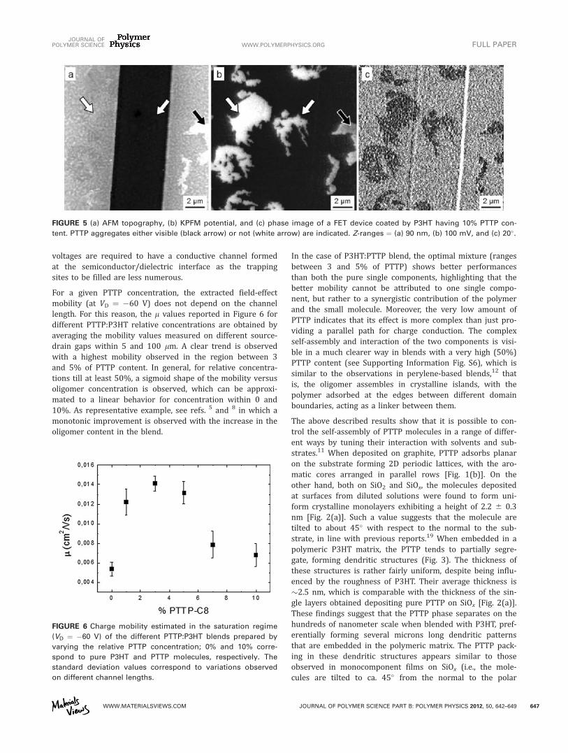
the different potential of PTTP with respect to P3HT isunambiguously displayed in Figure 4(b), and even more inFigure 4(d) (10% PTTP concentration), indicating that thedendritic structures are not just deposited over the polymermatrix but truly embedded into it. However, smaller yet stillvisible contrast can also be observed in the phase signal ofAFM images (Fig. 5).
The unambiguous SP difference between PTTP structure andits surrounding P3HT matrix makes it possible to visualizethe phase separation of the two components in the minimumrange of 30 nm (i.e., the lateral resolution of the techni-que).14(c) The measured SP values of self-assembled PTTPstructures (*) and the surrounding P3HT covered areas (n)are displayed in Figure 4(e). The SP of PTTP increases withthe concentration values up to 5%, whereas the potential of
the surrounding areas is still constant and equal to zero (i.e.,the potential of bare P3HT being set as reference value). Forhigher concentrations, a reverse trend is observed: the PTTPpotential is constant and in agreement with the value meas-ured on micrometric crystal, whereas the potential of theregions covered by P3HT increases. This evidence suggeststhat the two components are fully separated and that PTTPstructures are embedded into a P3HT matrix for concentra-tions smaller than 5%. For higher PTTP contents, taking intoaccount the increasing of the AFM roughness, the PTTPseems to form crystallites with a few tens of nanometer sizethat cannot be resolved by KPFM, although a global increas-ing of the measured potential is measured (see SupportingInformation).
KPFM is not known to be a purely surface-sensitive tech-nique as it has a sampling depth up to over 100 nm wheninvestigating semiconducting materials.18 Because of thisreason, PTTP assemblies covered by a thin layer of P3HT arehardly visible in AFM imaging, whereas they appear with avery good contrast in the SP map recorded by KPFM. It isworth noting that this sort of ‘‘bulk sensitivity’’ of the tech-nique means that the measured SP consists of a combinationof the SP of the two components: SPmeas ¼ a�SPP3HT þb�SPPTTP, where a þ b ¼ 1. Thus, using P3HT as reference(i.e., SPP3HT ¼ 0) is simply to evince that SPmeas ¼ b�SPPTTP< SPPTTP as experimentally observed.
Charge Transport in Transistor DevicesBottom-contact bottom-gate FETs were fabricated by depos-iting the PTTP:P3HT blends on SiO2 substrates exposing pre-patterned interdigitated source-drain gold electrodes on230-nm silicon oxide substrate. Alongside their electricalcharacterization, the devices were studied by AFM andKPFM. The morphology observed on prepatterned substrateswas not significantly different from the one observed onbare SiOx; because of the high Rrms, in some cases (Fig. 5),the PTTP phase was barely visible in the topography image,appearing only as an irregular rough, whereas KPFM showedthe typical branched structure, highlighting the need for acomplete characterization of such complex morphology withdifferent techniques.
The field-effect mobility l was determined from the satura-tion regime using the relationship between the drain current(ID) and the gate voltage (VG) from the following equation:
ID ¼ WCox2L
l VG � VThð Þ2;
where VTh is the threshold voltage, Cox is the capacitance/unit area of the oxide layer amounting to 1.63 � 10�8 F/cm2, and W and L represent the channel width and length,respectively. The threshold voltage shifts from slightly posi-tive toward lower values (in module) with increasing thePTTP content in the blend as shown in Supporting Informa-tion Figure S5. This latter trend suggests that a progressivelyhigher amount of crystalline domain/aggregates in the filmleads to a lower number of morphological defects and conse-quently trapping centers for the charge carriers. Thus, lower
FIGURE 4 (a and c) AFM and (b and d) corresponding KPFM
images of PTTP:P3HT blend with PTTP concentration of (a and
b) 1% and (c and d) 10%. (e) Measured SP of blend compo-
nents by varying the concentration within 1 and 10%: P3HT
(black filled squares) and PTTP (open gray circles) phases. Dot-
ted lines represent the potentials of bare P3HT (arbitrarily cho-
sen as reference value and set equal to 0) and bare PTTP. Z-
646 JOURNAL OF POLYMER SCIENCE PART B: POLYMER PHYSICS 2012, 50, 642–649
voltages are required to have a conductive channel formedat the semiconductor/dielectric interface as the trappingsites to be filled are less numerous.
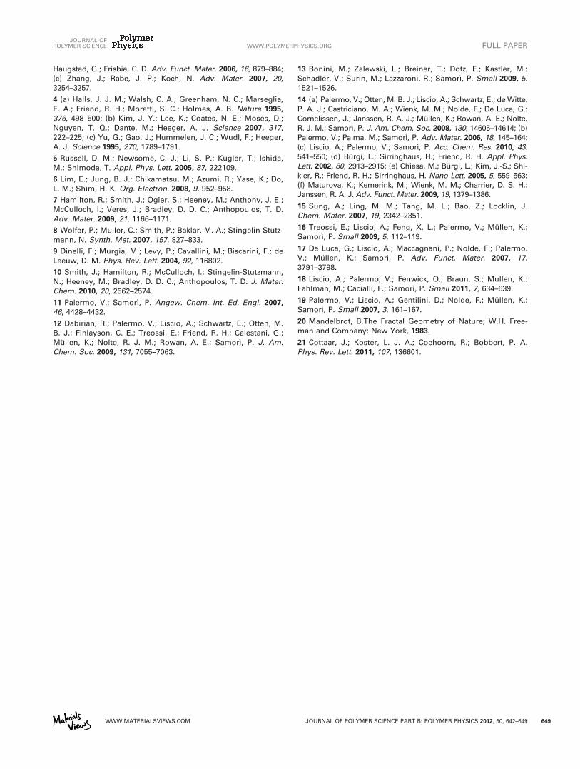
For a given PTTP concentration, the extracted field-effectmobility (at VD ¼ �60 V) does not depend on the channellength. For this reason, the l values reported in Figure 6 fordifferent PTTP:P3HT relative concentrations are obtained byaveraging the mobility values measured on different source-drain gaps within 5 and 100 lm. A clear trend is observedwith a highest mobility observed in the region between 3and 5% of PTTP content. In general, for relative concentra-tions till at least 50%, a sigmoid shape of the mobility versusoligomer concentration is observed, which can be approxi-mated to a linear behavior for concentration within 0 and10%. As representative example, see refs. 5 and 8 in which amonotonic improvement is observed with the increase in theoligomer content in the blend.
In the case of P3HT:PTTP blend, the optimal mixture (rangesbetween 3 and 5% of PTTP) shows better performancesthan both the pure single components, highlighting that thebetter mobility cannot be attributed to one single compo-nent, but rather to a synergistic contribution of the polymerand the small molecule. Moreover, the very low amount ofPTTP indicates that its effect is more complex than just pro-viding a parallel path for charge conduction. The complexself-assembly and interaction of the two components is visi-ble in a much clearer way in blends with a very high (50%)PTTP content (see Supporting Information Fig. S6), which issimilar to the observations in perylene-based blends,12 thatis, the oligomer assembles in crystalline islands, with thepolymer adsorbed at the edges between different domainboundaries, acting as a linker between them.
The above described results show that it is possible to con-trol the self-assembly of PTTP molecules in a range of differ-ent ways by tuning their interaction with solvents and sub-strates.11 When deposited on graphite, PTTP adsorbs planaron the substrate forming 2D periodic lattices, with the aro-matic cores arranged in parallel rows [Fig. 1(b)]. On theother hand, both on SiO2 and SiOx, the molecules depositedat surfaces from diluted solutions were found to form uni-form crystalline monolayers exhibiting a height of 2.2 6 0.3nm [Fig. 2(a)]. Such a value suggests that the molecule aretilted to about 45� with respect to the normal to the sub-strate, in line with previous reports.19 When embedded in apolymeric P3HT matrix, the PTTP tends to partially segre-gate, forming dendritic structures (Fig. 3). The thickness ofthese structures is rather fairly uniform, despite being influ-enced by the roughness of P3HT. Their average thickness is�2.5 nm, which is comparable with the thickness of the sin-gle layers obtained depositing pure PTTP on SiOx [Fig. 2(a)].These findings suggest that the PTTP phase separates on thehundreds of nanometer scale when blended with P3HT, pref-erentially forming several microns long dendritic patternsthat are embedded in the polymeric matrix. The PTTP pack-ing in these dendritic structures appears similar to thoseobserved in monocomponent films on SiOx (i.e., the mole-cules are tilted to ca. 45� from the normal to the polar
FIGURE 6 Charge mobility estimated in the saturation regime
(VD ¼ �60 V) of the different PTTP:P3HT blends prepared by
varying the relative PTTP concentration; 0% and 10% corre-
spond to pure P3HT and PTTP molecules, respectively. The
standard deviation values correspond to variations observed
on different channel lengths.
FIGURE 5 (a) AFM topography, (b) KPFM potential, and (c) phase image of a FET device coated by P3HT having 10% PTTP con-
tent. PTTP aggregates either visible (black arrow) or not (white arrow) are indicated. Z-ranges ¼ (a) 90 nm, (b) 100 mV, and (c) 20�.
JOURNAL OFPOLYMER SCIENCE WWW.POLYMERPHYSICS.ORG FULL PAPER
WWW.MATERIALSVIEWS.COM JOURNAL OF POLYMER SCIENCE PART B: POLYMER PHYSICS 2012, 50, 642–649 647
substrate). In case when the patterns are ‘‘exposed’’ on thesample surface, they can also be visible in topographic AFMimages, whereas when they are ‘‘buried’’ into the polymer, theyare detected only by KPFM or AFM phase imaging (Fig. 5).
KPFM reveals that while the SP of the polymeric phase remainsunchanged, the SP of the dendrites increases significantly withPTTP concentration up to 5–7% of PTTP content, saturatingfor higher values. To quantify the irregular shape of dendrites,we define the ‘‘shape factor’’: the ratio between the perimeter(p) and the square root of the area (A): D ¼ p=
ffiffiffi
Ap
.20 In thecase of regular polygons, D value decreases with the increas-ing number of the sides of the regular polygonal structurevarying between about 4.56 and about 1.13, that is, from thetriangle to the circle. Differently, dendrites show fractalstructures having higher D values corresponding to highinterdiffusion of the monomer into the polymer. The surfacecoverage of the PTTP dendrites increases with the monomerconcentration (from 0 to 5% PTTP content), together withthe increasing SP of the PTTP, whereas the dendrite shaperemains quite constant (as revealed by an unchanged D ¼15 6 5). In such a range, we observe a threefold enhance-ment of the charge mobility within the blend, highlightingthe beneficial effects of PTTP in the improvement of thecharge transport, in particular by providing more and morespatially extended preferential paths around bottlenecks anddefects in the polymeric layer with the increasing content ofPTTP. By further increasing the PTTP content (>7%), theconcentration of PTTP in the dendrites increases while theshape factor decreases. Moreover, the variation of the meas-ured SP of the film surrounding the dendrites suggests thepresence of sub-microcrystallites spread into the ‘‘polymericmatrix,’’ which cannot be resolved by either AFM due to thehigh surface roughness. The uniform potential measured inKPFM images suggests that the crystallites are dipped intothe polymer matrix and their size is smaller than about 100nm. When the PTTP concentrations amounts to 10%, theself-assembly changes drastically: (i) the dendrites becomepurely made of PTTP materials with quite regular shape (theshape factor lies between about 3 and 6) and (ii) we observethe formation of small (<500 nm), elongated crystallitesthat, though, worsen charge mobility, bringing it down, closeto the pure P3HT values. The decrease in the charge carriermobility can be ascribed to the increase of the boundaryregions between PTTP and P3HT leading to an enhancedcontact resistance at their interfaces.
Overall, the beneficial effect of PTTP on charge mobility isneither due to the formation of highly crystalline structuresnor due to the uniform dispersion of the small molecule intothe polymeric matrix. It can rather be ascribed to the crea-tion of highly branched, irregular percolation paths, in whichboth molecules are present; best results are obtained with aPTTP concentration ranging from 3 to 5%, when the concen-tration of the small molecule is high enough to create thesepaths, but not too much to induce a complete phase segrega-tion. A recent theoretical work of Cottaar et al.21 showedthat the charge transport in the molecular semiconductorcan be described by a scaling theory based on fat percola-
tion, showing that the charge transport does not monotoni-cally decrease with the increase in the uncorrelated Gaussiandisorder width. The obtained results on blend can be pic-tured in terms of this theoretical work. The increasing of thelength of PTTP-P3HT boundaries (within the PTTP phasesegregation) corresponds to an increasing of the electronicinterfaces states picture and the maximum of the achievedcharge transport corresponds to a bit amount of ‘‘disorder.’’
CONCLUSIONS
We studied the self-assembly of a blend of a bisphenyl-bithiophene molecule with P3HT on SiOx and correlated thenanoscale and macroscale morphologies with the electricproperties of the bicomponent material when incorporatedinto a FET. The small molecule was found to form microme-ter-sized aggregates that can act as percolation paths in thepolymeric matrix. By varying the content of the small mole-cule in the blend, it was possible to tune the compositionand electrical properties of the semiconducting film. Whencompared with the P3HT transistor, the blend exhibited animprovement of a factor of three in the charge mobility. Thebicomponent approach to FET appears as a viable solutionto best exploit the properties of small molecules and poly-meric materials toward high-performing devices.
ACKNOWLEDGMENTS
This work was supported by the EC ITN-SUPERIOR (PITN-GA-2009-238177), the EC FP7 ONE-P large-scale project no.212311, and the International Center for Frontier Research inChemistry (FRC, Strasbourg).
REFERENCES AND NOTES
1 (a) Tsao, H. N.; Cho, D.; Andreasen, J. W.; Rouhanipour, A.;
Breiby, D. W.; Pisula, W.; Mullen, K. Adv. Mater. 2009, 21,
209–212; (b) McCulloch, I.; Heeney, M.; Bailey, C.; Genevicius,
K.; Macdonald, I.; Shkunov, M.; Sparrowe, D.; Tierney, S.; Wag-
ner, R.; Zhang, W. M.; Chabinyc, M. L.; Kline, R. J.; McGehee,
M. D.; Toney, M. F. Nat. Mater. 2006, 5, 328–333; (c) Salleo, A.