Page 1
In-Situ Measurement of the Relative Thermal Contributions of Chemical Reactions and Ions During Plasma Etching
Plasma and CVD Processes 17
213th Meeting of the Electrochemical Society
M.R. Tesauro Qimonda Dresden GmbH & Co. OHG, Germany
G.A. Roche KLA-Tencor, SensArray Division
Page 2
Qimonda · Tesauro, Roche · Plasma and CVD Processes 17, 213th Meeting of the Electrochemical Society · Page 2 Copyright © Qimonda AG 2008 · All rights reserved.
Overview
Background: Chemical + Physical RemovalBackground: Chemical + Physical Removal
Results and DiscussionResults and Discussion
ConclusionsConclusions
Experimental MethodExperimental Method
Page 3
Qimonda · Tesauro, Roche · Plasma and CVD Processes 17, 213th Meeting of the Electrochemical Society · Page 3 Copyright © Qimonda AG 2008 · All rights reserved.
Background: Chemical + Physical RemovalBackground: Chemical + Physical Removal
Results and DiscussionResults and Discussion
ConclusionsConclusions
Experimental MethodExperimental Method
Page 4
Qimonda · Tesauro, Roche · Plasma and CVD Processes 17, 213th Meeting of the Electrochemical Society · Page 4 Copyright © Qimonda AG 2008 · All rights reserved.
Chemical & Physical Removal
J.W. Coburn, H. Winters J. Appl. Phys 50(5) May 1979
• Synergistic Effects- Chemical � Species� Temperature
- Physical� Ion Current� Ion Energy
• Synergistic Effects- Chemical � Species� Temperature
- Physical� Ion Current� Ion Energy
Page 5
Qimonda · Tesauro, Roche · Plasma and CVD Processes 17, 213th Meeting of the Electrochemical Society · Page 5 Copyright © Qimonda AG 2008 · All rights reserved.
Attributes of Substrate Temperature Measurement
• Heat in- Ion current (incl.
recombination)- Heat of condensation- Exothermic reactions- Process gas convection- Radiation
• Heat in- Ion current (incl.
recombination)- Heat of condensation- Exothermic reactions- Process gas convection- Radiation
• Heat Out- Convection to process gas - Loss through electrostatic
chuck- Radiation
• Heat Out- Convection to process gas - Loss through electrostatic
chuck- Radiation
Tsubstrate = Heat in - Heat OutTsubstrate = Heat in - Heat Out
Page 6
Qimonda · Tesauro, Roche · Plasma and CVD Processes 17, 213th Meeting of the Electrochemical Society · Page 6 Copyright © Qimonda AG 2008 · All rights reserved.
Why we care about this topic
• Evidently temperature spatial correlation to CD var iation.
• Routine recipe variation does not change response.
• Many hardware components are potentially responsibl e
• Objective: Identify mechanism and cut troubleshooti ng time.
• Evidently temperature spatial correlation to CD var iation.
• Routine recipe variation does not change response.
• Many hardware components are potentially responsibl e
• Objective: Identify mechanism and cut troubleshooti ng time.
Sensor Wafer Temperature
Sensor Wafer TemperatureIn-line CDIn-line CD
Page 7
Qimonda · Tesauro, Roche · Plasma and CVD Processes 17, 213th Meeting of the Electrochemical Society · Page 7 Copyright © Qimonda AG 2008 · All rights reserved.
Background: Chemical + Physical RemovalBackground: Chemical + Physical Removal
Results and DiscussionResults and Discussion
ConclusionsConclusions
Experimental MethodExperimental Method
Page 8
Qimonda · Tesauro, Roche · Plasma and CVD Processes 17, 213th Meeting of the Electrochemical Society · Page 8 Copyright © Qimonda AG 2008 · All rights reserved.
Sensorwafer Description
VRF ~Vs·ns·ω2
Page 9
Qimonda · Tesauro, Roche · Plasma and CVD Processes 17, 213th Meeting of the Electrochemical Society · Page 9 Copyright © Qimonda AG 2008 · All rights reserved.
Sensor Wafer Pre-Processing
Integral Sensor WaferCoated with 3um PFR IX420Hi-line Resist, 2mm EBR
Manual Solvent Removalof Resist on Wafer HalfLeft of Notch
Data Not UsedData Not Used
"Resist" Sensor Group
"Resist" Sensor Group
"No Resist" Sensor Group"No Resist"
Sensor Group
Page 10
Qimonda · Tesauro, Roche · Plasma and CVD Processes 17, 213th Meeting of the Electrochemical Society · Page 10 Copyright © Qimonda AG 2008 · All rights reserved.
Tem
pera
ture
Time
Si Tavg, steady-state (sensors on bare Si half)
Resist Tavg, steady-state (sensors on resist coated half)
∆Tss avg = k1A( Φr – ΦSi)∆Tss avg = k1A( Φr – ΦSi)
Assumption: for resist etch highly selective to Si: (Φr – ΦSi) = Heat of Chemical Reaction
Assumption: for resist etch highly selective to Si: (Φr – ΦSi) = Heat of Chemical Reaction
Exothermic Chemical Etch Components: Measurement Theory
Page 11
Qimonda · Tesauro, Roche · Plasma and CVD Processes 17, 213th Meeting of the Electrochemical Society · Page 11 Copyright © Qimonda AG 2008 · All rights reserved.
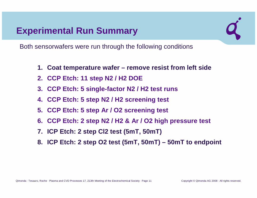
Experimental Run Summary
1. Coat temperature wafer – remove resist from left s ide
2. CCP Etch: 11 step N2 / H2 DOE
3. CCP Etch: 5 single-factor N2 / H2 test runs
4. CCP Etch: 5 step N2 / H2 screening test
5. CCP Etch: 5 step Ar / O2 screening test
6. CCP Etch: 2 step N2 / H2 & Ar / O2 high pressure test
7. ICP Etch: 2 step Cl2 test (5mT, 50mT)
8. ICP Etch: 2 step O2 test (5mT, 50mT) – 50mT to end point
Both sensorwafers were run through the following conditions
Page 12
Qimonda · Tesauro, Roche · Plasma and CVD Processes 17, 213th Meeting of the Electrochemical Society · Page 12 Copyright © Qimonda AG 2008 · All rights reserved.
Sensorwafer data traces
N2H2,30mT
O2Ar,30mT
POR, 100W, 300W, FRC-11, FRC+5 POR, 100W, 300W, FRC-11, FRC+5
O2Ar
200W,200mT
N2H2
200W, 200mT
Temperature
POR100W
300W
FRC-11 FRC+5
Vrf
CCP reactor
P=200mT, 200Wb,
a)N2=200, H2=250,
b) Ar=100, O2=10
Page 13
Qimonda · Tesauro, Roche · Plasma and CVD Processes 17, 213th Meeting of the Electrochemical Society · Page 13 Copyright © Qimonda AG 2008 · All rights reserved.
Background: Chemical + Physical RemovalBackground: Chemical + Physical Removal
Results and DiscussionResults and Discussion
ConclusionsConclusions
Experimental MethodExperimental Method
Page 14
Qimonda · Tesauro, Roche · Plasma and CVD Processes 17, 213th Meeting of the Electrochemical Society · Page 14 Copyright © Qimonda AG 2008 · All rights reserved.
Exothermic Chemical Etch Components: Experimental Data
N2 / H2 Chemistry: CCP Etch Chamber
43.8
44.0
44.2
44.4
44.6
44.8
45.0
1 6 11 16 21 26 31 36 41 46 51 56 61 66
Time (s)
Tem
p (C
)
1. Exponential Data Fit
2. Extrapolate to Steady-State
3. Calculate ( Φr – ΦSi)
4. Estimate removal rate based on C-C bond strength
1. Exponential Data Fit
2. Extrapolate to Steady-State
3. Calculate ( Φr – ΦSi)
4. Estimate removal rate based on C-C bond strength
Page 15
Qimonda · Tesauro, Roche · Plasma and CVD Processes 17, 213th Meeting of the Electrochemical Society · Page 15 Copyright © Qimonda AG 2008 · All rights reserved.
N2 / H2 Chemistry: CCP Etch Chamber
43.8
44.0
44.2
44.4
44.6
44.8
45.0
1 6 11 16 21 26 31 36 41 46 51 56 61 66
Time (s)
Tem
p (C
) Bare SiBare Si
ResistResist
• However, the Si half of sensorwafer was hotter!
• Assumption is that thick resist (~3 µm) acts as an insulator to ion bombardment
• However, the Si half of sensorwafer was hotter!
• Assumption is that thick resist (~3 µm) acts as an insulator to ion bombardment
Exothermic Chemical Etch Components: Experimental Data
Page 16
Qimonda · Tesauro, Roche · Plasma and CVD Processes 17, 213th Meeting of the Electrochemical Society · Page 16 Copyright © Qimonda AG 2008 · All rights reserved.
Etch Rate / Vrf and Temperature Response to RF Power (CCP chamber)
CCP, Ar / O2
120013001400150016001700180019002000
50 150 250 350
13 MHz RF Power (W)
Vrf
(V)
70
80
90
100
110
120
Etc
h R
ate
(nm
/ m
in)
CCP Ar / O2
44.4
44.6
44.8
45
45.2
45.4
45.6
50 150 250 350
13 MHz RF Power (W)
Ste
p T
max
(C
)
Resist
Si
Both Etch rate and Vrf show strong response to RF B ias power.Temperature has a modest response to RF power. This data supports the notion that Etch Rate is dom inated by physical mechanism.
Both Etch rate and Vrf show strong response to RF B ias power.Temperature has a modest response to RF power. This data supports the notion that Etch Rate is dom inated by physical mechanism.
Page 17
Qimonda · Tesauro, Roche · Plasma and CVD Processes 17, 213th Meeting of the Electrochemical Society · Page 17 Copyright © Qimonda AG 2008 · All rights reserved.
Sensorwafer Response: Resist ClearingMean temperature by half wafer zones …
Now that resist is thinned ( ≤ 550 nm), resist half runs hotter than bare Si.Temperatures of each half converge as resist clears .Now that resist is thinned ( ≤ 550 nm), resist half runs hotter than bare Si.Temperatures of each half converge as resist clears .
Time (s)
… ICP reactor, 50mT O2 Clearing Resist from sensorwaf er
Page 18
Qimonda · Tesauro, Roche · Plasma and CVD Processes 17, 213th Meeting of the Electrochemical Society · Page 18 Copyright © Qimonda AG 2008 · All rights reserved.
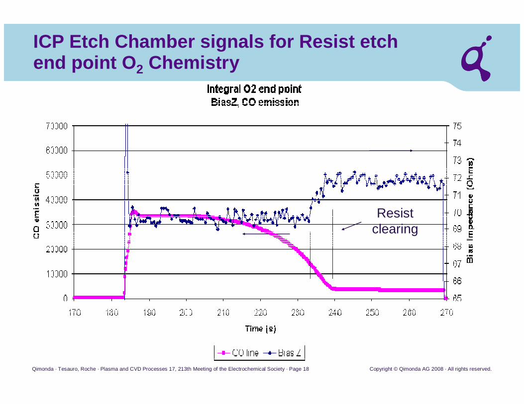
ICP Etch Chamber signals for Resist etch end point O 2 Chemistry
Resist clearing
Page 19
Qimonda · Tesauro, Roche · Plasma and CVD Processes 17, 213th Meeting of the Electrochemical Society · Page 19 Copyright © Qimonda AG 2008 · All rights reserved.
Etch-to-Clear Resist, 50mT O 2(All sensors, same scale throughout)
RF on 176sRF on 176s clearing
"Hot spot" disappears as resist clears"Hot spot" disappears as resist clears
RESSi
Page 20
Qimonda · Tesauro, Roche · Plasma and CVD Processes 17, 213th Meeting of the Electrochemical Society · Page 20 Copyright © Qimonda AG 2008 · All rights reserved.
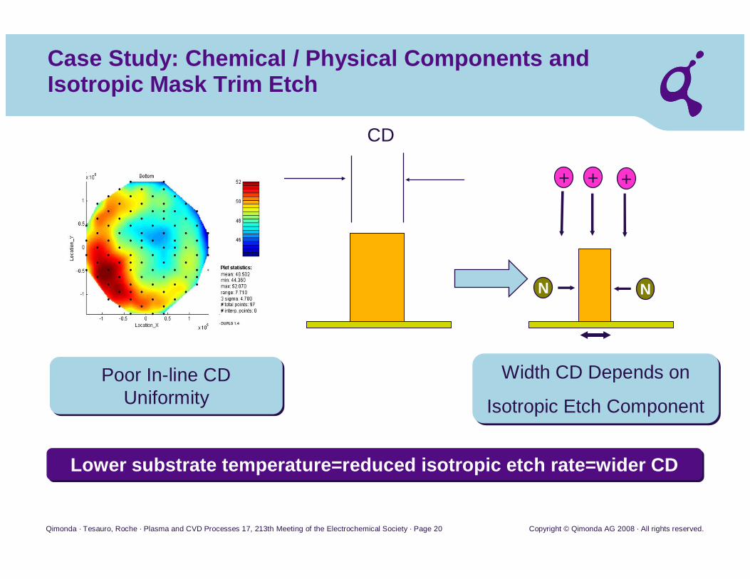
Case Study: Chemical / Physical Components and Isotropic Mask Trim Etch
Width CD Depends on
Isotropic Etch Component
Width CD Depends on
Isotropic Etch Component
Poor In-line CD Uniformity
Poor In-line CD Uniformity
+ + +
CD
Lower substrate temperature=reduced isotropic etch rate=wider CDLower substrate temperature=reduced isotropic etch rate=wider CD
NN
Page 21
Qimonda · Tesauro, Roche · Plasma and CVD Processes 17, 213th Meeting of the Electrochemical Society · Page 21 Copyright © Qimonda AG 2008 · All rights reserved.
Case Study: Root Cause Identification
Poor In-line CD Uniformity
Poor In-line CD Uniformity
Temperature Vrf Temperature Vrf
Sensorwafer responseSensorwafer response
“Heat Out” problemnot “Heat In”
“Heat Out” problemnot “Heat In”
Page 22
Qimonda · Tesauro, Roche · Plasma and CVD Processes 17, 213th Meeting of the Electrochemical Society · Page 22 Copyright © Qimonda AG 2008 · All rights reserved.
Correction Verification
Poor In-line CD Uniformity
Poor In-line CD Uniformity Temp 20C Cathode Temp 40C Cathode
range = 10 C range = 3.5 C
Temp 20C Cathode Temp 40C Cathode
range = 10 C range = 3.5 C
Sensorwafer responseSensorwafer response
CD non-uniformity problem localized to heating/cool ing apparatus of ESCCD non-uniformity problem localized to heating/cool ing apparatus of ESC
Page 23
Qimonda · Tesauro, Roche · Plasma and CVD Processes 17, 213th Meeting of the Electrochemical Society · Page 23 Copyright © Qimonda AG 2008 · All rights reserved.
Background: Chemical + Physical RemovalBackground: Chemical + Physical Removal
Results and DiscussionResults and Discussion
ConclusionsConclusions
Experimental MethodExperimental Method
Page 24
Qimonda · Tesauro, Roche · Plasma and CVD Processes 17, 213th Meeting of the Electrochemical Society · Page 24 Copyright © Qimonda AG 2008 · All rights reserved.
Conclusions / Summary
The Resist/Bare Sensorwafer Method Shows Promise
• Can detect small but consistent differences in temp erature
and Could benefit from:
• Thinner coating for improved sensitivity
• "Checkerboard" pattern to avoid chamber-related asy mmetries
• Examine isotropic removal vs. vertical removal
Use of Temperature & Volt Sensorwafers together is proving useful
• Quickly ascertain source of chamber asymmetry
Page 25
Qimonda · Tesauro, Roche · Plasma and CVD Processes 17, 213th Meeting of the Electrochemical Society · Page 25 Copyright © Qimonda AG 2008 · All rights reserved.
Acknowledgements
AcknowledgementsAcknowledgements
Professor Costas Spanos The University of California, Berkeley
Matthias VoigtLithography Track Expert
Qimonda Dresden GmbH & Co. OHG
Professor Costas Spanos The University of California, Berkeley
Matthias VoigtLithography Track Expert
Qimonda Dresden GmbH & Co. OHG
Page 26
Thank you
The World's LeadingCreative Memory Company
Page 27
Qimonda · Tesauro, Roche · Plasma and CVD Processes 17, 213th Meeting of the Electrochemical Society · Page 27 Copyright © Qimonda AG 2008 · All rights reserved.
Page 28
Qimonda · Tesauro, Roche · Plasma and CVD Processes 17, 213th Meeting of the Electrochemical Society · Page 28 Copyright © Qimonda AG 2008 · All rights reserved.
Page 29
Qimonda · Tesauro, Roche · Plasma and CVD Processes 17, 213th Meeting of the Electrochemical Society · Page 29 Copyright © Qimonda AG 2008 · All rights reserved.
50mT O2