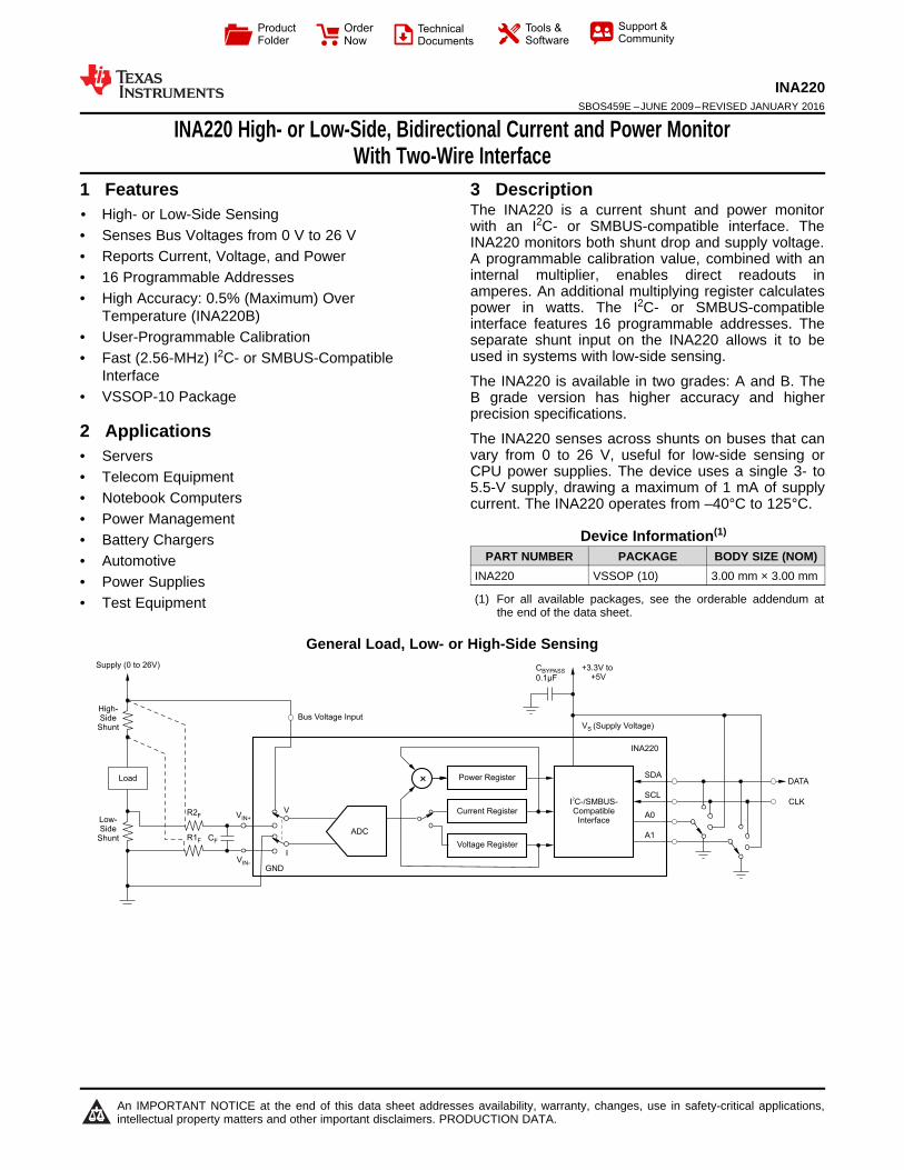
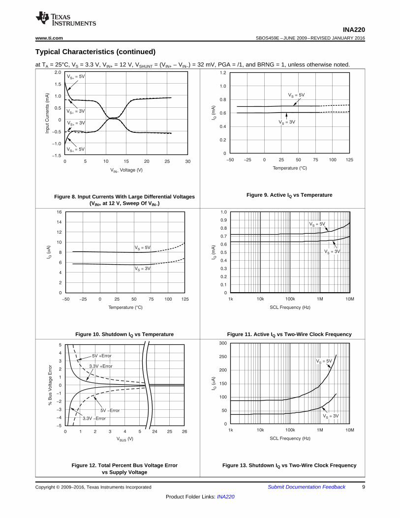
× Power Register Current Register I C-/SMBUS- 2 Compatible Interface Voltage Register V (Supply Voltage) S ADC INA220 GND V I V IN+ V IN- A0 A1 SDA DATA SCL CLK C BYPASS 0.1μF +3.3V to +5V Bus Voltage Input High- Side Shunt Low- Side Shunt R1 F R2 F C F Load Supply (0 to 26V) Product Folder Order Now Technical Documents Tools & Software Support & Community An IMPORTANT NOTICE at the end of this data sheet addresses availability, warranty, changes, use in safety-critical applications, intellectual property matters and other important disclaimers. PRODUCTION DATA. INA220 SBOS459E – JUNE 2009 – REVISED JANUARY 2016 INA220 High- or Low-Side, Bidirectional Current and Power Monitor With Two-Wire Interface 1 1 Features 1• High- or Low-Side Sensing • Senses Bus Voltages from 0 V to 26 V • Reports Current, Voltage, and Power • 16 Programmable Addresses • High Accuracy: 0.5% (Maximum) Over Temperature (INA220B) • User-Programmable Calibration • Fast (2.56-MHz) I 2 C- or SMBUS-Compatible Interface • VSSOP-10 Package 2 Applications • Servers • Telecom Equipment • Notebook Computers • Power Management • Battery Chargers • Automotive • Power Supplies • Test Equipment 3 Description The INA220 is a current shunt and power monitor with an I 2 C- or SMBUS-compatible interface. The INA220 monitors both shunt drop and supply voltage. A programmable calibration value, combined with an internal multiplier, enables direct readouts in amperes. An additional multiplying register calculates power in watts. The I 2 C- or SMBUS-compatible interface features 16 programmable addresses. The separate shunt input on the INA220 allows it to be used in systems with low-side sensing. The INA220 is available in two grades: A and B. The B grade version has higher accuracy and higher precision specifications. The INA220 senses across shunts on buses that can vary from 0 to 26 V, useful for low-side sensing or CPU power supplies. The device uses a single 3- to 5.5-V supply, drawing a maximum of 1 mA of supply current. The INA220 operates from –40°C to 125°C. Device Information (1) PART NUMBER PACKAGE BODY SIZE (NOM) INA220 VSSOP (10) 3.00 mm × 3.00 mm (1) For all available packages, see the orderable addendum at the end of the data sheet. General Load, Low- or High-Side Sensing
Transcript
× Power Register
Current RegisterI C-/SMBUS-2
CompatibleInterface
Voltage Register
V (Supply Voltage)S
ADC
INA220
GND
V
I
VIN+
VIN-
A0
A1
SDADATA
SCLCLK
CBYPASS
0.1µF
+3.3V to+5V
Bus Voltage InputHigh-Side
Shunt
Low-Side
Shunt R1F
R2F
CF
Load
Supply (0 to 26V)
Product
Folder
Order
Now
Technical
Documents
Tools &
Software
Support &Community
An IMPORTANT NOTICE at the end of this data sheet addresses availability, warranty, changes, use in safety-critical applications,intellectual property matters and other important disclaimers. PRODUCTION DATA.
INA220SBOS459E –JUNE 2009–REVISED JANUARY 2016
INA220 High- or Low-Side, Bidirectional Current and Power MonitorWith Two-Wire Interface
1
1 Features1• High- or Low-Side Sensing• Senses Bus Voltages from 0 V to 26 V• Reports Current, Voltage, and Power• 16 Programmable Addresses• High Accuracy: 0.5% (Maximum) Over
Temperature (INA220B)• User-Programmable Calibration• Fast (2.56-MHz) I2C- or SMBUS-Compatible
Interface• VSSOP-10 Package
2 Applications• Servers• Telecom Equipment• Notebook Computers• Power Management• Battery Chargers• Automotive• Power Supplies• Test Equipment
3 DescriptionThe INA220 is a current shunt and power monitorwith an I2C- or SMBUS-compatible interface. TheINA220 monitors both shunt drop and supply voltage.A programmable calibration value, combined with aninternal multiplier, enables direct readouts inamperes. An additional multiplying register calculatespower in watts. The I2C- or SMBUS-compatibleinterface features 16 programmable addresses. Theseparate shunt input on the INA220 allows it to beused in systems with low-side sensing.
The INA220 is available in two grades: A and B. TheB grade version has higher accuracy and higherprecision specifications.
The INA220 senses across shunts on buses that canvary from 0 to 26 V, useful for low-side sensing orCPU power supplies. The device uses a single 3- to5.5-V supply, drawing a maximum of 1 mA of supplycurrent. The INA220 operates from –40°C to 125°C.
Device Information(1)
PART NUMBER PACKAGE BODY SIZE (NOM)INA220 VSSOP (10) 3.00 mm × 3.00 mm
(1) For all available packages, see the orderable addendum atthe end of the data sheet.
10 Power Supply Recommendations ..................... 2911 Layout................................................................... 29
11.1 Layout Guidelines ................................................. 2911.2 Layout Example .................................................... 29
12 Device and Documentation Support ................. 3012.1 Related Documentation......................................... 3012.2 Community Resources.......................................... 3012.3 Trademarks ........................................................... 3012.4 Electrostatic Discharge Caution............................ 3012.5 Glossary ................................................................ 30
13 Mechanical, Packaging, and OrderableInformation ........................................................... 30
4 Revision HistoryNOTE: Page numbers for previous revisions may differ from page numbers in the current version.
Changes from Revision D (September 2010) to Revision E Page
• Added ESD Ratings table, Feature Description section, Device Functional Modes section, Application andImplementation section, Power Supply Recommendations section, Layout section, Device and DocumentationSupport section, and Mechanical, Packaging, and Orderable Information section ............................................................... 1
• Changed front page diagram. ................................................................................................................................................ 1• Changed pin names in the pin description. ............................................................................................................................ 4• Changed the temperature values in the Absolute Maximum Ratings table ........................................................................... 5• Changed Ambient temperature from –25 to –40 in the MIN column. .................................................................................... 5• Deleted Temperature Range parameters from Electrical Characteristics. ............................................................................. 7• Changed I2C timing spec change based on characterization data. ...................................................................................... 7
Changes from Revision C (September, 2009) to Revision D Page
• Changed High Accuracy bullet in Features from 1% to 0.5% for B-grade device.................................................................. 1• Added new paragraph to Description regarding A- and B-grade versions of the device ....................................................... 1• Added new row to Packaging Information table to show new B-grade device ...................................................................... 4• Added B-grade columns in Electrical Characteristics for MIN, TYP and MAX values ........................................................... 6• Changed Current Sense Gain Error over temperature specification from 10 ppm/°C to 1m%/°C......................................... 6• Added Configure/Measure/Calculate Example..................................................................................................................... 25
INA209 Current/power monitor with watchdog, peak-hold, and fast comparator functions
INA210, INA211, INA212, INA213, INA214 Zero-drift, low-cost, analog current shunt monitor series in small package
INA219 Zero-drift, bidirectional current power monitor with two-wire interface
6 Pin Configuration and Functions
DGS Package10-PIN VSSOP
Top View
Pin FunctionsPIN
I/O DESCRIPTIONNAME NO.A1 1 Digital Input Address pin. Connect to GND, SCL, SDA, or VS. Table 1 shows pin settings and corresponding addresses.A0 2 Digital Input Address pin. Connect to GND, SCL, SDA, or VS. Table 1 shows pin settings and corresponding addresses.NC 3 — No internal connectionSDA 4 Digital I/O Serial bus data lineSCL 5 Digital Input Serial bus clock lineVS 6 Analog Power supply, 3 V to 5.5 VGND 7 Analog GroundVBUS 8 Analog Input Bus voltage input
IN– 9 Analog Input Negative differential shunt voltage. Connect to negative side of shunt resistor. Bus voltage is measuredfrom this pin to ground.
IN+ 10 Analog Input Positive differential shunt voltage. Connect to positive side of shunt resistor.
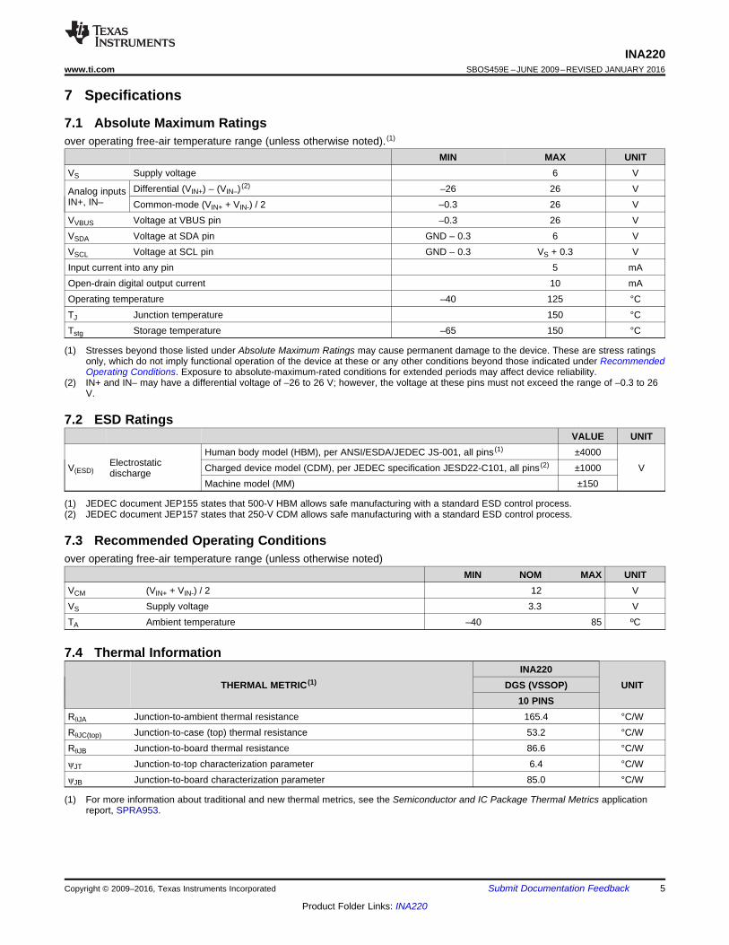
(1) Stresses beyond those listed under Absolute Maximum Ratings may cause permanent damage to the device. These are stress ratingsonly, which do not imply functional operation of the device at these or any other conditions beyond those indicated under RecommendedOperating Conditions. Exposure to absolute-maximum-rated conditions for extended periods may affect device reliability.
(2) IN+ and IN– may have a differential voltage of –26 to 26 V; however, the voltage at these pins must not exceed the range of –0.3 to 26V.
7 Specifications
7.1 Absolute Maximum Ratingsover operating free-air temperature range (unless otherwise noted). (1)
VVBUS Voltage at VBUS pin –0.3 26 VVSDA Voltage at SDA pin GND – 0.3 6 VVSCL Voltage at SCL pin GND – 0.3 VS + 0.3 VInput current into any pin 5 mAOpen-drain digital output current 10 mAOperating temperature –40 125 °CTJ Junction temperature 150 °CTstg Storage temperature –65 150 °C
(1) JEDEC document JEP155 states that 500-V HBM allows safe manufacturing with a standard ESD control process.(2) JEDEC document JEP157 states that 250-V CDM allows safe manufacturing with a standard ESD control process.
7.2 ESD RatingsVALUE UNIT
V(ESD)Electrostaticdischarge
Human body model (HBM), per ANSI/ESDA/JEDEC JS-001, all pins (1) ±4000VCharged device model (CDM), per JEDEC specification JESD22-C101, all pins (2) ±1000
Machine model (MM) ±150
7.3 Recommended Operating Conditionsover operating free-air temperature range (unless otherwise noted)
MIN NOM MAX UNITVCM (VIN+ + VIN-) / 2 12 VVS Supply voltage 3.3 VTA Ambient temperature –40 85 ºC
(1) For more information about traditional and new thermal metrics, see the Semiconductor and IC Package Thermal Metrics applicationreport, SPRA953.
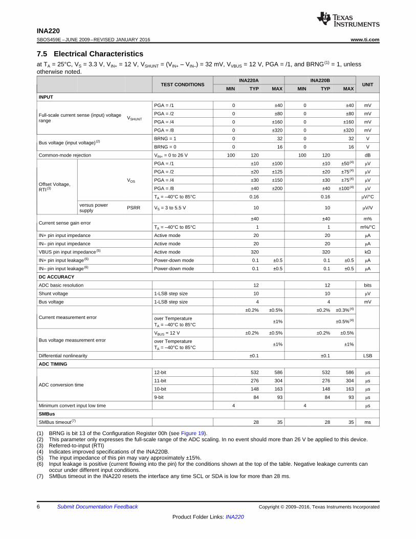
(1) BRNG is bit 13 of the Configuration Register 00h (see Figure 19).(2) This parameter only expresses the full-scale range of the ADC scaling. In no event should more than 26 V be applied to this device.(3) Referred-to-input (RTI)(4) Indicates improved specifications of the INA220B.(5) The input impedance of this pin may vary approximately ±15%.(6) Input leakage is positive (current flowing into the pin) for the conditions shown at the top of the table. Negative leakage currents can
occur under different input conditions.(7) SMBus timeout in the INA220 resets the interface any time SCL or SDA is low for more than 28 ms.
VIL input logic level –0.3 0.3 (VS) –0.3 0.3 (VS) V
Hysteresis 500 500 mV
OPEN-DRAIN DIGITAL OUTPUTS (SDA)
Logic 0 output level ISINK = 3 mA 0.15 0.4 0.15 0.4 V
High-level output leakage current VOUT = VS 0.1 1 0.1 1 μA
POWER SUPPLY
Operating supply range 3 5.5 3 5.5 V
Quiescent current 0.7 1 0.7 1 mA
Quiescent current, power-down mode 6 15 6 15 μA
Power-on reset threshold 2 2 V
(1) Values based on a statistical analysis of a one-time sample of devices. Minimum and maximum values are not ensured and notproduction tested. Condition: A0=A1=0.
7.6 Bus Timing Diagram Definitions (1)
FAST MODE HIGH-SPEED MODEUNIT
MIN TYP MAX MIN TYP MAXƒ(SCL) SCL operating frequency 0.001 0.4 0.001 2.56 MHz
t(BUF)Bus free time between STOP and STARTcondition 1300 160 ns
t(HDSTA)
Hold time after repeated START conditionAfter this period, the first clock isgenerated.
600 160 ns
t(SUSTA) Repeated START condition setup time 600 160 nst(SUSTO) STOP condition setup time 600 160 nst(HDDAT) Data hold time 0 900 0 90 nst(SUDAT) Data setup time 100 10 nst(LOW) SCL clock LOW period 1300 250 nst(HIGH) SCL clock HIGH period 600 60 nstFDA Data fall time 300 150 nstFCL Clock fall time 300 40 nstRCL Clock rise time 300 40 nstRCL Clock rise time for SCLK ≤ 100 kHz 1000 ns
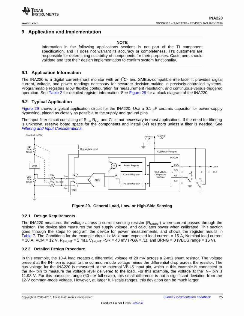
8.1 OverviewThe INA220 is a digital current sense amplifier with an I2C- and SMBus-compatible interface. It provides digitalcurrent, voltage, and power readings necessary for accurate decision-making in precisely-controlled systems.Programmable registers allow flexible configuration for measurement resolution as well as continuous-versus-triggered operation. Detailed register information appears at the end of this data sheet, beginning with Table 2.See Functional Block Diagram for a block diagram of the INA220 device.
8.2 Functional Block Diagram
8.3 Feature Description
8.3.1 Basic ADC FunctionsThe two analog inputs to the INA220, IN+ and IN–, connect to a shunt resistor in the bus of interest. Bus voltageis measured at VBUS pin. The INA220 is typically powered by a separate supply from 3 to 5.5 V. The bus beingsensed can vary from 0 to 26 V. It requires no special considerations for power-supply sequencing (for example,a bus voltage can be present with the supply voltage off, and vice-versa). The INA220 senses the small dropacross the shunt for shunt voltage, and senses the voltage with respect to ground from VBUS pin for the busvoltage.
When the INA220 is in the normal operating mode (that is, MODE bits of the Configuration register are set to111), it continuously converts the shunt voltage up to the number set in the shunt voltage averaging function(Configuration register, SADC bits). The device then converts the bus voltage up to the number set in the busvoltage averaging (Configuration register, BADC bits). The Mode control in the Configuration register alsopermits selecting modes to convert only voltage or current, either continuously or in response to an event(triggered).
All current and power calculations are performed in the background and do not contribute to conversion time;conversion times shown in Electrical Characteristics can be used to determine the actual conversion time.
Power-down mode reduces the quiescent current and turns off current into the INA220 inputs, avoiding anysupply drain. Full recovery from power-down requires 40 μs. ADC off mode (set by the Configuration register,MODE bits) stops all conversions.
In triggered mode, writing any of the triggered convert modes into the Configuration register (even if the desiredmode is already programmed into the register) triggers a single-shot conversion.
Feature Description (continued)Although the INA220 can be read at any time, and the data from the last conversion remain available, theConversion Ready bit (Status register, CNVR bit) is provided to help coordinate one-shot or triggeredconversions. The Conversion Ready bit is set after all conversions, averaging, and multiplication operations arecomplete.
The Conversion Ready bit clears under any of these conditions:• Writing to the Configuration register, except when configuring the MODE bits for power down or ADC off
(disable) modes• Reading the Status register• Triggering a single-shot conversion with the convert pin
8.3.1.1 Power MeasurementCurrent and bus voltage are converted at different points in time, depending on the resolution and averagingmode settings. For instance, when configured for 12-bit and 128-sample averaging, up to 68 ms in time betweensampling these two values is possible. Again, these calculations are performed in the background and do not addto the overall conversion time.
8.3.1.2 PGA FunctionIf larger full-scale shunt voltages are desired, the INA220 provides a PGA function that increases the full-scalerange up to 2, 4, or 8 times (320 mV). Additionally, the bus voltage measurement has two full-scale ranges: 16 or32 V.
8.3.1.3 Compatibility With TI Hot Swap ControllersThe INA220 is designed for compatibility with hot swap controllers such the TI TPS2490. The TPS2490 uses ahigh-side shunt with a limit at 50 mV; the INA220 full-scale range of 40 mV enables the use of the same shunt forcurrent sensing below this limit. When sensing is required at (or through) the 50-mV sense point of the TPS2490,the PGA of the INA220 can be set to /2 to provide an 80-mV full-scale range.
8.4 Device Functional Modes
8.4.1 Filtering and Input ConsiderationsMeasuring current is often noisy, and such noise can be difficult to define. The INA220 offers several options forfiltering by choosing resolution and averaging in the Configuration register. These filtering options can be setindependently for either voltage or current measurement.
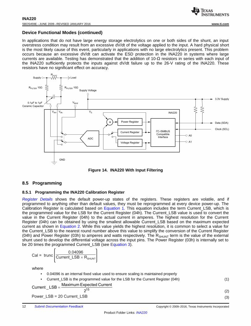
The internal ADC is based on a delta-sigma (ΔΣ) front-end with a 500-kHz (±30%) typical sampling rate. Thisarchitecture has good inherent noise rejection; however, transients that occur at or very close to the samplingrate harmonics can cause problems. Because these signals are at 1 MHz and higher, they can be dealt with byincorporating filtering at the input of the INA220. The high frequency enables the use of low-value series resistorson the filter for negligible effects on measurement accuracy. In general, filtering the INA220 input is onlynecessary if there are transients at exact harmonics of the 500-kHz (±30%) sampling rate (>1 MHz). Filter usingthe lowest possible series resistance and ceramic capacitor. TI recommends values of 0.1 to 1 μF. Figure 14shows the INA220 with an additional filter added at the input.
Overload conditions are another consideration for the INA220 inputs. The INA220 inputs are specified to tolerate26 V across the inputs. A large differential scenario might be a short to ground on the load side of the shunt. Thistype of event can result in full power-supply voltage across the shunt (as long the power supply or energystorage capacitors support it). It must be remembered that removing a short to ground can result in inductivekickbacks that could exceed the 26-V differential and common-mode rating of the INA220. Inductive kickbackvoltages are best dealt with by Zener-type transient-absorbing devices combined with sufficient energy storagecapacitance.
Device Functional Modes (continued)In applications that do not have large energy storage electrolytics on one or both sides of the shunt, an inputoverstress condition may result from an excessive dV/dt of the voltage applied to the input. A hard physical shortis the most likely cause of this event, particularly in applications with no large electrolytics present. This problemoccurs because an excessive dV/dt can activate the ESD protection in the INA220 in systems where largecurrents are available. Testing has demonstrated that the addition of 10-Ω resistors in series with each input ofthe INA220 sufficiently protects the inputs against dV/dt failure up to the 26-V rating of the INA220. Theseresistors have no significant effect on accuracy.
Figure 14. INA220 With Input Filtering
8.5 Programming
8.5.1 Programming the INA220 Calibration RegisterRegister Details shows the default power-up states of the registers. These registers are volatile, and ifprogrammed to anything other than default values, they must be reprogrammed at every device power-up. TheCalibration Register is calculated based on Equation 1. This equation includes the term Current_LSB, which isthe programmed value for the LSB for the Current Register (04h). The Current_LSB value is used to convert thevalue in the Current Register (04h) to the actual current in amperes. The highest resolution for the CurrentRegister (04h) can be obtained by using the smallest allowable Current_LSB based on the maximum expectedcurrent as shown in Equation 2. While this value yields the highest resolution, it is common to select a value forthe Current_LSB to the nearest round number above this value to simplify the conversion of the Current Register(04h) and Power Register (03h) to amperes and watts respectively. The RSHUNT term is the value of the externalshunt used to develop the differential voltage across the input pins. The Power Register (03h) is internally set tobe 20 times the programmed Current_LSB (see Equation 3).
where• 0.04096 is an internal fixed value used to ensure scaling is maintained properly• Current_LSB is the programmed value for the LSB for the Current Register (04h) (1)
Programming (continued)Shunt voltage is calculated by multiplying the Shunt Voltage Register contents with the Shunt Voltage LSB of 10μV. The Bus Voltage register bits are not right-aligned. To compute the value of the Bus Voltage, Bus VoltageRegister contents must be shifted right by three bits. This shift puts the BD0 bit in the LSB position so that thecontents can be multiplied by the Bus Voltage LSB of 4-mV to compute the bus voltage measured by the device.After programming the Calibration Register, the value expected in the Current Register (04h) can be calculatedby multiplying the Shunt Voltage register contents by the Calibration Register and then dividing by 4096 asshown in Equation 4. To obtain a value in amperes, the Current register value is multiplied by the programmedCurrent_LSB.
(4)
The value expected in the Power register (03h) can be calculated by multiplying the Current register value by theBus Voltage register value and then dividing by 5000 as shown in Equation 5. Power Register content ismultiplied by Power LSB which is 20 times the Current_LSB for a power value in watts.
(5)
8.5.2 Programming the INA220 Power Measurement Engine
8.5.2.1 Calibration Register and ScalingThe Calibration register makes it possible to set the scaling of the Current and Power registers to whatevervalues are most useful for a given application. One strategy may be to set the Calibration register such that thelargest possible number is generated in the Current register or Power register at the expected full-scale point;this approach yields the highest resolution. The Calibration register can also be selected to provide values in theCurrent and Power registers that either provide direct decimal equivalents of the values being measured, or yielda round LSB number. After these choices have been made, the Calibration register also offers possibilities forend-user system-level calibration, where the value is adjusted slightly to cancel total system error. Afterdetermining the exact current by using an external ammeter, the value of the Calibration Register can then beadjusted based on the measured current result of the INA220 to cancel the total system error as shown inEquation 6.
(6)
8.5.3 Simple Current Shunt Monitor Usage (No Programming Necessary)The INA220 can be used without any programming if it is only necessary to read a shunt voltage drop and busvoltage with the default 12-bit resolution, 320-mV shunt full-scale range (PGA = /8), 32-V bus full-scale range,and continuous conversion of shunt and bus voltage.
Without programming, current is measured by reading the shunt voltage. The Current register and Power registerare only available if the Calibration register contains a programmed value.
8.5.4 Bus OverviewThe INA220 offers compatibility with both I2C and SMBus interfaces. The I2C and SMBus protocols areessentially compatible with one another.
The I2C interface is used throughout this data sheet as the primary example, with SMBus protocol specified onlywhen a difference between the two systems is being addressed. Two lines, SCL and SDA, connect the INA220to the bus. Both SCL and SDA are open-drain connections.
The device that initiates the transfer is called a master, and the devices controlled by the master are slaves. Thebus must be controlled by a master device that generates the serial clock (SCL), controls the bus access, andgenerates START and STOP conditions.
Programming (continued)To address a specific device, the master initiates a START condition by pulling the data signal line (SDA) from ahigh to a low logic level while SCL is high. All slaves on the bus shift in the slave address byte on the rising edgeof SCL, with the last bit indicating whether a read or write operation is intended. During the ninth clock pulse, theslave being addressed responds to the master by generating an Acknowledge and pulling SDA low.
Data transfer is then initiated and eight bits of data are sent, followed by an Acknowledge bit. During datatransfer, SDA must remain stable while SCL is high. Any change in SDA while SCL is high is interpreted as aSTART or STOP condition.
After all data have been transferred, the master generates a STOP condition, indicated by pulling SDA from lowto high while SCL is high. The INA220 includes a 28-ms timeout on its interface to prevent locking up an SMBus.
8.5.4.1 Serial Bus AddressTo communicate with the INA220, the master must first address slave devices through a slave address byte. Theslave address byte consists of seven address bits, and a direction bit indicating the intent of executing a read orwrite operation.
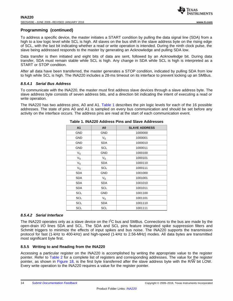
The INA220 has two address pins, A0 and A1. Table 1 describes the pin logic levels for each of the 16 possibleaddresses. The state of pins A0 and A1 is sampled on every bus communication and should be set before anyactivity on the interface occurs. The address pins are read at the start of each communication event.
GND GND 1000000GND VS 1000001GND SDA 1000010GND SCL 1000011VS GND 1000100VS VS 1000101VS SDA 1000110VS SCL 1000111
SDA GND 1001000SDA VS 1001001SDA SDA 1001010SDA SCL 1001011SCL GND 1001100SCL VS 1001101SCL SDA 1001110SCL SCL 1001111
8.5.4.2 Serial InterfaceThe INA220 operates only as a slave device on the I2C bus and SMBus. Connections to the bus are made by theopen-drain I/O lines SDA and SCL. The SDA and SCL pins feature integrated spike suppression filters andSchmitt triggers to minimize the effects of input spikes and bus noise. The INA220 supports the transmissionprotocol for fast (1-kHz to 400-kHz) and high-speed (1-kHz to 2.56-MHz) modes. All data bytes are transmittedmost significant byte first.
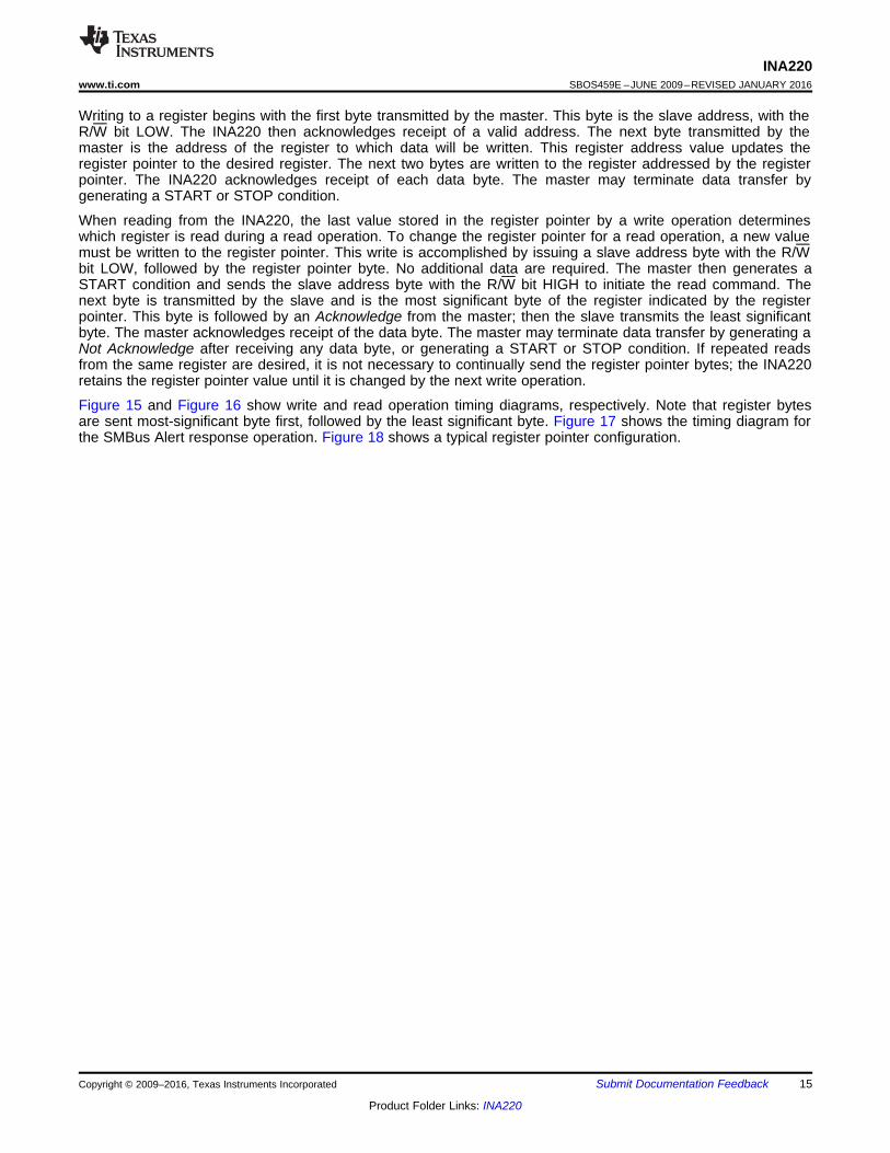
8.5.5 Writing to and Reading from the INA220Accessing a particular register on the INA220 is accomplished by writing the appropriate value to the registerpointer. Refer to Table 2 for a complete list of registers and corresponding addresses. The value for the registerpointer, as shown in Figure 18, is the first byte transferred after the slave address byte with the R/W bit LOW.Every write operation to the INA220 requires a value for the register pointer.
Writing to a register begins with the first byte transmitted by the master. This byte is the slave address, with theR/W bit LOW. The INA220 then acknowledges receipt of a valid address. The next byte transmitted by themaster is the address of the register to which data will be written. This register address value updates theregister pointer to the desired register. The next two bytes are written to the register addressed by the registerpointer. The INA220 acknowledges receipt of each data byte. The master may terminate data transfer bygenerating a START or STOP condition.
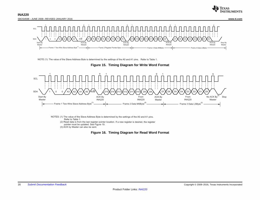
When reading from the INA220, the last value stored in the register pointer by a write operation determineswhich register is read during a read operation. To change the register pointer for a read operation, a new valuemust be written to the register pointer. This write is accomplished by issuing a slave address byte with the R/Wbit LOW, followed by the register pointer byte. No additional data are required. The master then generates aSTART condition and sends the slave address byte with the R/W bit HIGH to initiate the read command. Thenext byte is transmitted by the slave and is the most significant byte of the register indicated by the registerpointer. This byte is followed by an Acknowledge from the master; then the slave transmits the least significantbyte. The master acknowledges receipt of the data byte. The master may terminate data transfer by generating aNot Acknowledge after receiving any data byte, or generating a START or STOP condition. If repeated readsfrom the same register are desired, it is not necessary to continually send the register pointer bytes; the INA220retains the register pointer value until it is changed by the next write operation.
Figure 15 and Figure 16 show write and read operation timing diagrams, respectively. Note that register bytesare sent most-significant byte first, followed by the least significant byte. Figure 17 shows the timing diagram forthe SMBus Alert response operation. Figure 18 shows a typical register pointer configuration.
(1) Values based on a statistical analysis of a one-time sample of devices. Minimum and maximum values are not ensured and notproduction tested. Condition: A0=A1=0.
(1) Type: R = Read only, R/W = Read/Write.(2) The Power register and Current register default to 0 because the Calibration register defaults to 0, yielding a zero current value until the
Calibration register is programmed.
8.5.5.1 High-Speed Two-Wire ModeWhen the bus is idle, both the SDA and SCL lines are pulled high by the pullup devices. The master generates astart condition followed by a valid serial byte containing high-speed (HS) master code 00001XXX. Thistransmission is made in fast (400 kbps) or standard (100 kbps) (F/S) mode at no more than 400 kbps. TheINA220 does not acknowledge the HS master code, but does recognize it and switches its internal filters tosupport 2.56-Mbps operation.
The master then generates a repeated start condition (a repeated start condition has the same timing as the startcondition). After this repeated start condition, the protocol is the same as F/S mode, except that transmissionspeeds up to 2.56 Mbps are allowed. Instead of using a stop condition, repeated start conditions should be usedto secure the bus in HS-mode. A STOP condition ends the HS-mode and switches all the internal filters of theINA220 to support the F/S mode. See Bus Timing Diagram Definitions (1) and Figure 1 for timing.
8.5.5.2 Power-Up ConditionsPower-up conditions apply to a software reset through the RST bit (bit 15) in the Configuration register, or the I2Cbus General Call Reset.
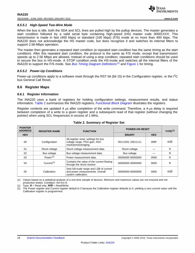
8.6 Register Maps
8.6.1 Register InformationThe INA220 uses a bank of registers for holding configuration settings, measurement results, and statusinformation. Table 2 summarizes the INA220 registers; Functional Block Diagram illustrates the registers.
Register contents are updated 4 μs after completion of the write command. Therefore, a 4-μs delay is requiredbetween completion of a write to a given register and a subsequent read of that register (without changing thepointer) when using SCL frequencies in excess of 1 MHz.
Table 2. Summary of Register SetPOINTERADDRESS REGISTER NAME FUNCTION
POWER-ON RESETTYPE (1)
HEX BINARY HEX
00 ConfigurationAll-register reset, settings for busvoltage range, PGA gain, ADCresolution/averaging.
00111001 10011111 399F R/W
01 Shunt voltage Shunt voltage measurement data. Shunt voltage — R02 Bus voltage Bus voltage measurement data. Bus voltage — R03 Power (2) Power measurement data. 00000000 00000000 0000 R
04 Current (2) Contains the value of the current flowingthrough the shunt resistor. 00000000 00000000 0000 R
05 CalibrationSets full-scale range and LSB of currentand power measurements. Overallsystem calibration.
LEGEND: R/W = Read/Write; R = Read only; -n = value after reset
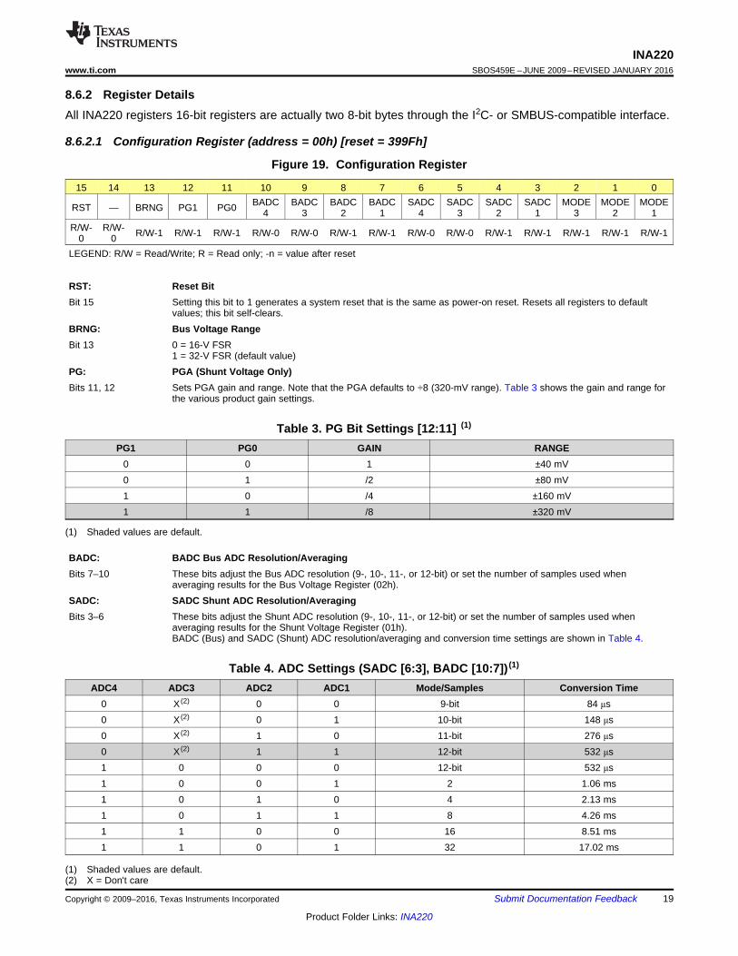
RST: Reset BitBit 15 Setting this bit to 1 generates a system reset that is the same as power-on reset. Resets all registers to default
values; this bit self-clears.BRNG: Bus Voltage RangeBit 13 0 = 16-V FSR
1 = 32-V FSR (default value)PG: PGA (Shunt Voltage Only)Bits 11, 12 Sets PGA gain and range. Note that the PGA defaults to ÷8 (320-mV range). Table 3 shows the gain and range for
BADC: BADC Bus ADC Resolution/AveragingBits 7–10 These bits adjust the Bus ADC resolution (9-, 10-, 11-, or 12-bit) or set the number of samples used when
averaging results for the Bus Voltage Register (02h).SADC: SADC Shunt ADC Resolution/AveragingBits 3–6 These bits adjust the Shunt ADC resolution (9-, 10-, 11-, or 12-bit) or set the number of samples used when
averaging results for the Shunt Voltage Register (01h).BADC (Bus) and SADC (Shunt) ADC resolution/averaging and conversion time settings are shown in Table 4.
MODE: Operating ModeBits 0–2 Selects continuous, triggered, or power-down mode of operation. These bits default to continuous shunt and bus
measurement mode. The mode settings are shown in Table 5.
(1) Shaded values are default.
Table 5. Mode Settings [2:0] (1)
MODE3 MODE2 MODE1 MODE0 0 0 Power-down0 0 1 Shunt voltage, triggered0 1 0 Bus voltage, triggered0 1 1 Shunt and bus, triggered1 0 0 ADC off (disabled)1 0 1 Shunt voltage, continuous1 1 0 Bus voltage, continuous1 1 1 Shunt and bus, continuous
8.6.3 Data Output Registers
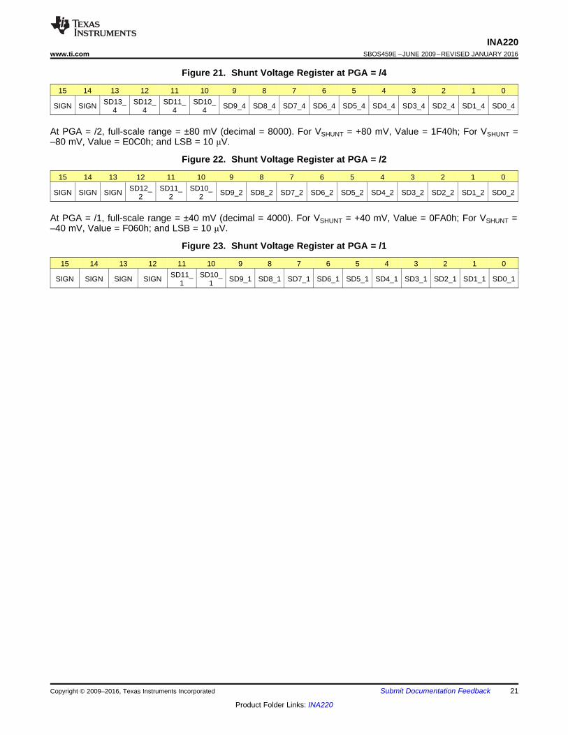
8.6.3.1 Shunt Voltage Register (address = 01h)The Shunt Voltage register stores the current shunt voltage reading, VSHUNT. Shunt Voltage register bits areshifted according to the PGA setting selected in the Configuration register (00h). When multiple sign bits arepresent, they are all the same value. Negative numbers are represented in 2's complement format. Generate the2's complement of a negative number by complementing the absolute value binary number and adding 1. Extendthe sign, denoting a negative number by setting the MSB = 1. Extend the sign to any additional sign bits to formthe 16-bit word.
Example: For a value of VSHUNT = –320 mV:1. Take the absolute value (include accuracy to 0.01 mV) → 320.002. Translate this number to a whole decimal number → 320003. Convert it to binary → 111 1101 0000 00004. Complement the binary result : 000 0010 1111 11115. Add 1 to the complement to create the 2's-complement formatted result → 000 0011 0000 00006. Extend the sign and create the 16-bit word: 1000 0011 0000 0000 = 8300h (Remember to extend the sign to
all sign-bits, as necessary based on the PGA setting.)
At PGA = /8, full-scale range = ±320 mV (decimal = 32000). For VSHUNT = +320 mV, Value = 7D00h; For VSHUNT= –320 mV, Value =8300h; and LSB = 10 μV.
CNVR: Conversion ReadyBit 1 Although the data from the last conversion can be read at any time, the INA220 Conversion Ready bit (CNVR)
indicates when data from a conversion is available in the data output registers. The CNVR bit is set after allconversions, averaging, and multiplications are complete. CNVR will clear under the following conditions:1.) Writing a new mode into the Operating Mode bits in the Configuration Register (except for Power-Down orDisable)2.) Reading the Power Register
OVF: Math Overflow FlagBit 0 The Math Overflow Flag (OVF) is set when the Power or Current calculations are out of range. It indicates that
current and power data may be meaningless.
8.6.3.3 Power Register (address = 03h) [reset = 00h]Full-scale range and LSB are set by the Calibration register. See Programming the INA220 Calibration Register.
LEGEND: R/W = Read/Write; R = Read only; -n = value after reset
The Power register records power in watts by multiplying the values of the current with the value of the busvoltage according to the Equation 5:
8.6.3.4 Current Register (address = 04h) [reset =00h]Full-scale range and LSB depend on the value entered in the Calibration register. See Programming the INA220Calibration Register. Negative values are stored in 2's complement format.
The value of the Current register is calculated by multiplying the value in the Shunt Voltage register with thevalue in the Calibration register according to the Equation 4.
8.6.4 Calibration Register
8.6.4.1 Calibration Register (address = 05h) [reset = 00h]Current and power calibration are set by bits FS15 to FS1 of the Calibration register. Note that bit FS0 is notused in the calculation. This register sets the current that corresponds to a full-scale drop across the shunt. Full-scale range and the LSB of the current and power measurement depend on the value entered in this register.See the Programming the INA220 Calibration Register. This register is suitable for use in overall systemcalibration. Note that the 0 POR values are all default.
(1) FS0 is a void bit and will always be 0. It is not possible to write a 1 to FS0. CALIBRATION is the value stored in FS15:FS1.
NOTEInformation in the following applications sections is not part of the TI componentspecification, and TI does not warrant its accuracy or completeness. TI’s customers areresponsible for determining suitability of components for their purposes. Customers shouldvalidate and test their design implementation to confirm system functionality.
9.1 Application InformationThe INA220 is a digital current-shunt monitor with an I2C- and SMBus-compatible interface. It provides digitalcurrent, voltage, and power readings necessary for accurate decision-making in precisely-controlled systems.Programmable registers allow flexible configuration for measurement resolution, and continuous-versus-triggeredoperation. See Table 2 for detailed register information. See Figure 29 for a block diagram of the INA220.
9.2 Typical ApplicationFigure 29 shows a typical application circuit for the INA220. Use a 0.1-μF ceramic capacitor for power-supplybypassing, placed as closely as possible to the supply and ground pins.
The input filter circuit consisting of RF1, RF2, and CF is not necessary in most applications. If the need for filteringis unknown, reserve board space for the components and install 0-Ω resistors unless a filter is needed. SeeFiltering and Input Considerations.
Figure 29. General Load, Low- or High-Side Sensing
9.2.1 Design RequirementsThe INA220 measures the voltage across a current-sensing resistor (RSHUNT) when current passes through theresistor. The device also measures the bus supply voltage, and calculates power when calibrated. This sectiongoes through the steps to program the device for power measurements, and shows the register results inTable 7. The Conditions for the example circuit is: Maximum expected load current = 15 A, Nominal load current= 10 A, VCM = 12 V, RSHUNT = 2 mΩ, VSHUNT FSR = 40 mV (PGA = /1), and BRNG = 0 (VBUS range = 16 V).
9.2.2 Detailed Design Procedure
In this example, the 10-A load creates a differential voltage of 20 mV across a 2-mΩ shunt resistor. The voltagepresent at the IN– pin is equal to the common-mode voltage minus the differential drop across the resistor. Thebus voltage for the INA220 is measured at the external VBUS input pin, which in this example is connected tothe IN– pin to measure the voltage level delivered to the load. For this example, the voltage at the IN– pin is11.98 V. For this particular range (40-mV full-scale), this small difference is not a significant deviation from the12-V common-mode voltage. However, at larger full-scale ranges, this deviation can be much larger.
Typical Application (continued)Note that the Bus Voltage register bits are not right-aligned. To compute the value of the Bus Voltage registercontents using the LSB of 4 mV, the register must be shifted right by three bits. This shift puts the BD0 bit in theLSB position so that the contents can be multiplied by the 4-mV LSB value to compute the bus voltage measuredby the device. The shifted value of the bus voltage register contents is now equal to BB3h, a decimal equivalentof 2995. This value of 2995 multiplied by the 4-mV LSB results in a value of 11.98 V.
The Calibration register (05h) is set to provide the device information about the current shunt resistor that wasused to create the measured shunt voltage. By knowing the value of the shunt resistor, the device can thencalculate the amount of current that created the measured shunt voltage drop. The first step when calculating thecalibration value is setting the current LSB. The Calibration register value is based on a calculation that has itsprecision capability limited by the size of the register and the Current register LSB. The device can measurebidirectional current; thus, the MSB of the Current register is a sign bit that allows for the rest of the 15 bits to beused for the Current register value. For this example, the minimum current LSB would be 457.78 µA/bit assuminga maximum expected current of 15 A using Equation 2. For this example, a value of 1 mA/bit was chosen for thecurrent LSB. Setting the current LSB to this value allows for sufficient precision while serving to simplify the mathas well. Using Equation 1 results in a Calibration register value of 20480 or 5000h.
The Current register (04h) is internally calculated by multiplying the shunt voltage contents by the Calibrationregister and then dividing by 4096 using Equation 4. For this example, the shunt voltage of 2000 is multiplied bythe Calibration register of 20480 and then divided by 4096 to yield a Current register value of 10000 (2710h).
The Power register (03h) is internally calculated by multiplying the Current register value of 10000 by the BusVoltage register value of 2995 and then dividing by 5000 using Equation 5. For this example, the Power registercontents are 5990 (1766h). Multiplying this result by the power LSB that is 20 times the 1 × 10⁻³ current LSB, or20 × 10–3, results in a power calculation of 5990 × 20 mW/bit, which equals 119.8 W. This result matches what isexpected for this register. A manual calculation for the power being delivered to the load would use 11.98 V(12 VCM – 20 mV shunt drop) multiplied by the load current of 10 A to give a 119.8-W result.
Calibration 05h 5000h 20480Current 04h 2710h 10000 1 mA 10.0 APower 03h 1766h 5990 20 mW 119.8 W
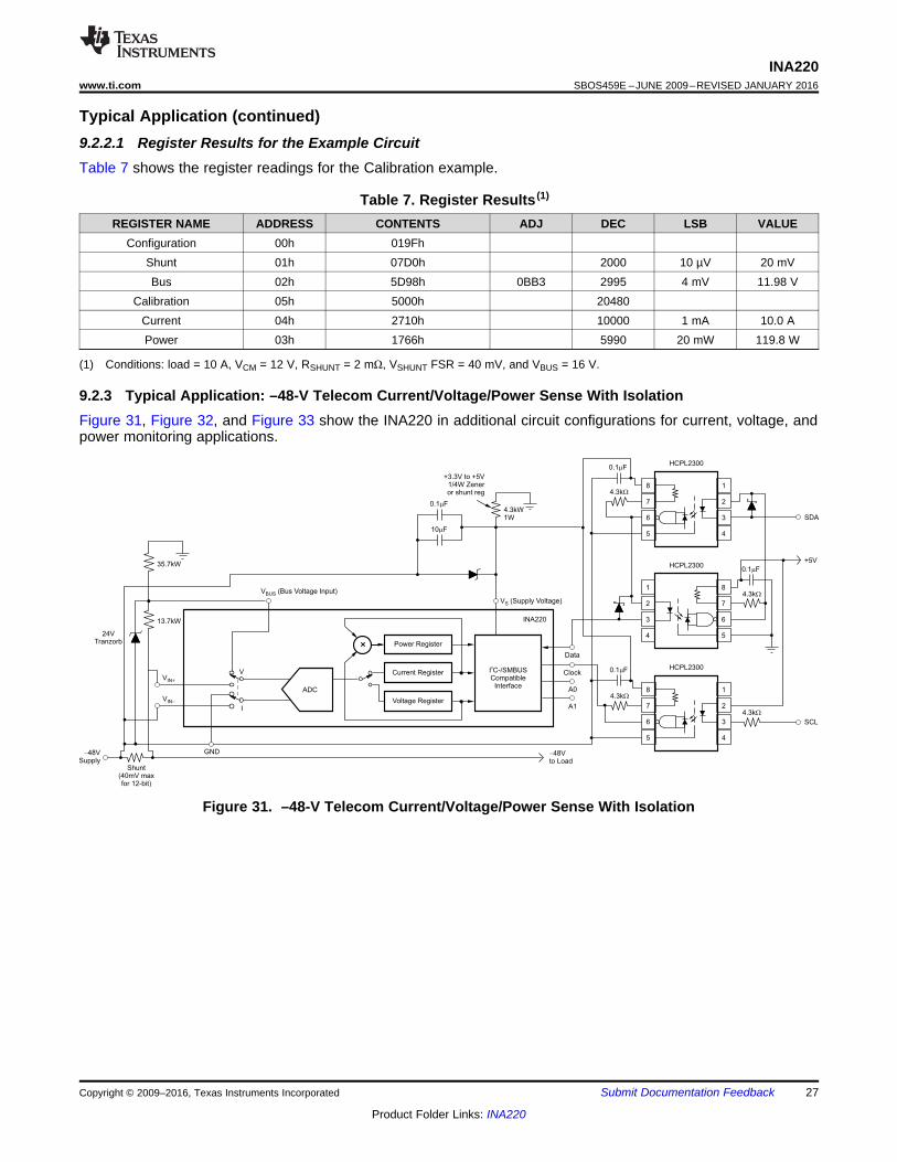
9.2.3 Typical Application: –48-V Telecom Current/Voltage/Power Sense With IsolationFigure 31, Figure 32, and Figure 33 show the INA220 in additional circuit configurations for current, voltage, andpower monitoring applications.
Figure 31. –48-V Telecom Current/Voltage/Power Sense With Isolation
10 Power Supply RecommendationsThe input circuitry of the device can accurately measure signals on common-mode voltages beyond its powersupply voltage, VS. For example, the voltage applied to the VS power supply terminal can be 5 V, whereas theload power-supply voltage being monitored (the common-mode voltage) can be as high as 26 V. Note also thatthe device can withstand the full 0-V to 26-V range at the input terminals, regardless of whether the device haspower applied or not. Place the required power-supply bypass capacitors as close as possible to the supply andground terminals of the device to ensure stability. A typical value for this supply bypass capacitor is 0.1 μF.Applications with noisy or high-impedance power supplies may require additional decoupling capacitors to rejectpower-supply noise.
11 Layout
11.1 Layout GuidelinesConnect the input pins (IN+ and IN–) to the sensing resistor using a Kelvin connection or a 4-wire connection.These connection techniques ensure that only the current-sensing resistor impedance is detected between theinput pins. Poor routing of the current-sensing resistor commonly results in additional resistance present betweenthe input pins. Given the very low ohmic value of the current-sensing resistor, any additional high-current carryingimpedance causes significant measurement errors. Place the power-supply bypass capacitor as close aspossible to the supply and ground pins.
12.1 Related DocumentationFor related documentation see the TPS2490/1 Positive High-Voltage Power-Limiting Hotswap Controller datasheet (SLVS503).
12.2 Community ResourcesThe following links connect to TI community resources. Linked contents are provided "AS IS" by the respectivecontributors. They do not constitute TI specifications and do not necessarily reflect TI's views; see TI's Terms ofUse.
TI E2E™ Online Community TI's Engineer-to-Engineer (E2E) Community. Created to foster collaborationamong engineers. At e2e.ti.com, you can ask questions, share knowledge, explore ideas and helpsolve problems with fellow engineers.
Design Support TI's Design Support Quickly find helpful E2E forums along with design support tools andcontact information for technical support.
12.3 TrademarksE2E is a trademark of Texas Instruments.All other trademarks are the property of their respective owners.
12.4 Electrostatic Discharge CautionThese devices have limited built-in ESD protection. The leads should be shorted together or the device placed in conductive foamduring storage or handling to prevent electrostatic damage to the MOS gates.
12.5 GlossarySLYZ022 — TI Glossary.
This glossary lists and explains terms, acronyms, and definitions.
13 Mechanical, Packaging, and Orderable InformationThe following pages include mechanical, packaging, and orderable information. This information is the mostcurrent data available for the designated devices. This data is subject to change without notice and revision ofthis document. For browser-based versions of this data sheet, refer to the left-hand navigation.
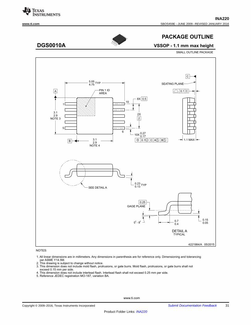
VSSOP - 1.1 mm max heightDGS0010ASMALL OUTLINE PACKAGE
NOTES:
1. All linear dimensions are in millimeters. Any dimensions in parenthesis are for reference only. Dimensioning and tolerancingper ASME Y14.5M.
2. This drawing is subject to change without notice.3. This dimension does not include mold flash, protrusions, or gate burrs. Mold flash, protrusions, or gate burrs shall not
exceed 0.15 mm per side.4. This dimension does not include interlead flash. Interlead flash shall not exceed 0.25 mm per side.5. Reference JEDEC registration MO-187, variation BA.
110
0.1 C A B
6
5
PIN 1 IDAREA
SEATING PLANE
0.1 C
SEE DETAIL A
TYPICALDETAIL A
SCALE 3.200
31
INA220www.ti.com SBOS459E –JUNE 2009–REVISED JANUARY 2016
VSSOP - 1.1 mm max heightDGS0010ASMALL OUTLINE PACKAGE
NOTES: (continued)
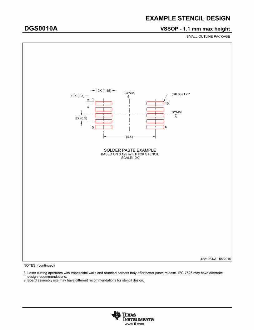
8. Laser cutting apertures with trapezoidal walls and rounded corners may offer better paste release. IPC-7525 may have alternatedesign recommendations.
9. Board assembly site may have different recommendations for stencil design.
SYMM
SYMM
1
5 6
10
BASED ON 0.125 mm THICK STENCILSOLDER PASTE EXAMPLE
SCALE:10X
33
INA220www.ti.com SBOS459E –JUNE 2009–REVISED JANUARY 2016
INA220AIDGSR ACTIVE VSSOP DGS 10 2500 RoHS & Green NIPDAU | NIPDAUAG Level-2-260C-1 YEAR -40 to 125 OOUI
INA220AIDGST ACTIVE VSSOP DGS 10 250 RoHS & Green NIPDAU | NIPDAUAG Level-2-260C-1 YEAR -40 to 125 OOUI
INA220BIDGSR ACTIVE VSSOP DGS 10 2500 RoHS & Green NIPDAU | NIPDAUAG Level-2-260C-1 YEAR -40 to 125 ZAEI
INA220BIDGST ACTIVE VSSOP DGS 10 250 RoHS & Green NIPDAU | NIPDAUAG Level-2-260C-1 YEAR -40 to 125 ZAEI
(1) The marketing status values are defined as follows:ACTIVE: Product device recommended for new designs.LIFEBUY: TI has announced that the device will be discontinued, and a lifetime-buy period is in effect.NRND: Not recommended for new designs. Device is in production to support existing customers, but TI does not recommend using this part in a new design.PREVIEW: Device has been announced but is not in production. Samples may or may not be available.OBSOLETE: TI has discontinued the production of the device.
(2) RoHS: TI defines "RoHS" to mean semiconductor products that are compliant with the current EU RoHS requirements for all 10 RoHS substances, including the requirement that RoHS substancedo not exceed 0.1% by weight in homogeneous materials. Where designed to be soldered at high temperatures, "RoHS" products are suitable for use in specified lead-free processes. TI mayreference these types of products as "Pb-Free".RoHS Exempt: TI defines "RoHS Exempt" to mean products that contain lead but are compliant with EU RoHS pursuant to a specific EU RoHS exemption.Green: TI defines "Green" to mean the content of Chlorine (Cl) and Bromine (Br) based flame retardants meet JS709B low halogen requirements of <=1000ppm threshold. Antimony trioxide basedflame retardants must also meet the <=1000ppm threshold requirement.
(3) MSL, Peak Temp. - The Moisture Sensitivity Level rating according to the JEDEC industry standard classifications, and peak solder temperature.
(4) There may be additional marking, which relates to the logo, the lot trace code information, or the environmental category on the device.
(5) Multiple Device Markings will be inside parentheses. Only one Device Marking contained in parentheses and separated by a "~" will appear on a device. If a line is indented then it is a continuationof the previous line and the two combined represent the entire Device Marking for that device.
(6) Lead finish/Ball material - Orderable Devices may have multiple material finish options. Finish options are separated by a vertical ruled line. Lead finish/Ball material values may wrap to twolines if the finish value exceeds the maximum column width.
Important Information and Disclaimer:The information provided on this page represents TI's knowledge and belief as of the date that it is provided. TI bases its knowledge and belief on informationprovided by third parties, and makes no representation or warranty as to the accuracy of such information. Efforts are underway to better integrate information from third parties. TI has taken and
continues to take reasonable steps to provide representative and accurate information but may not have conducted destructive testing or chemical analysis on incoming materials and chemicals.TI and TI suppliers consider certain information to be proprietary, and thus CAS numbers and other limited information may not be available for release.
In no event shall TI's liability arising out of such information exceed the total purchase price of the TI part(s) at issue in this document sold by TI to Customer on an annual basis.
OTHER QUALIFIED VERSIONS OF INA220 :
• Automotive: INA220-Q1
NOTE: Qualified Version Definitions:
• Automotive - Q100 devices qualified for high-reliability automotive applications targeting zero defects
VSSOP - 1.1 mm max heightDGS0010ASMALL OUTLINE PACKAGE
NOTES: 1. All linear dimensions are in millimeters. Any dimensions in parenthesis are for reference only. Dimensioning and tolerancing per ASME Y14.5M. 2. This drawing is subject to change without notice. 3. This dimension does not include mold flash, protrusions, or gate burrs. Mold flash, protrusions, or gate burrs shall not exceed 0.15 mm per side. 4. This dimension does not include interlead flash. Interlead flash shall not exceed 0.25 mm per side.5. Reference JEDEC registration MO-187, variation BA.
110
0.1 C A B
65
PIN 1 IDAREA
SEATING PLANE
0.1 C
SEE DETAIL A
DETAIL ATYPICAL
SCALE 3.200
www.ti.com
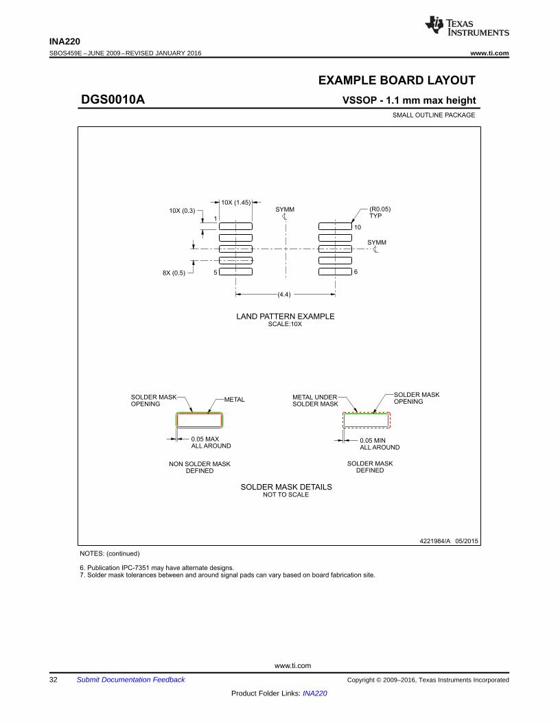
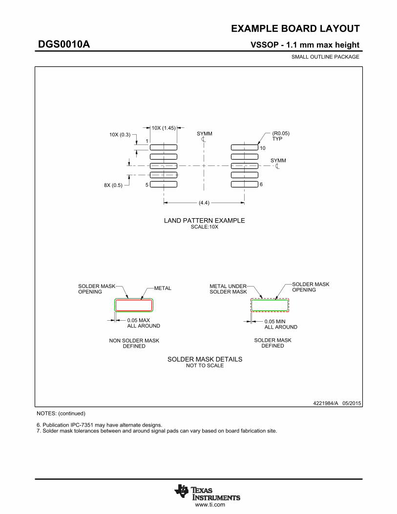
EXAMPLE BOARD LAYOUT
(4.4)
0.05 MAXALL AROUND
0.05 MINALL AROUND
10X (1.45)10X (0.3)
8X (0.5)
(R )TYP
0.05
4221984/A 05/2015
VSSOP - 1.1 mm max heightDGS0010ASMALL OUTLINE PACKAGE
SYMM
SYMM
LAND PATTERN EXAMPLESCALE:10X
1
5 6
10
NOTES: (continued) 6. Publication IPC-7351 may have alternate designs. 7. Solder mask tolerances between and around signal pads can vary based on board fabrication site.
METALSOLDER MASKOPENING
NON SOLDER MASKDEFINED
SOLDER MASK DETAILSNOT TO SCALE
SOLDER MASKOPENING
METAL UNDERSOLDER MASK
SOLDER MASKDEFINED
www.ti.com
EXAMPLE STENCIL DESIGN
(4.4)
8X (0.5)
10X (0.3)10X (1.45)
(R ) TYP0.05
4221984/A 05/2015
VSSOP - 1.1 mm max heightDGS0010ASMALL OUTLINE PACKAGE
NOTES: (continued) 8. Laser cutting apertures with trapezoidal walls and rounded corners may offer better paste release. IPC-7525 may have alternate design recommendations. 9. Board assembly site may have different recommendations for stencil design.
SYMM
SYMM
1
5 6
10
SOLDER PASTE EXAMPLEBASED ON 0.125 mm THICK STENCIL
SCALE:10X
IMPORTANT NOTICE AND DISCLAIMERTI PROVIDES TECHNICAL AND RELIABILITY DATA (INCLUDING DATASHEETS), DESIGN RESOURCES (INCLUDING REFERENCEDESIGNS), APPLICATION OR OTHER DESIGN ADVICE, WEB TOOLS, SAFETY INFORMATION, AND OTHER RESOURCES “AS IS”AND WITH ALL FAULTS, AND DISCLAIMS ALL WARRANTIES, EXPRESS AND IMPLIED, INCLUDING WITHOUT LIMITATION ANYIMPLIED WARRANTIES OF MERCHANTABILITY, FITNESS FOR A PARTICULAR PURPOSE OR NON-INFRINGEMENT OF THIRDPARTY INTELLECTUAL PROPERTY RIGHTS.These resources are intended for skilled developers designing with TI products. You are solely responsible for (1) selecting the appropriateTI products for your application, (2) designing, validating and testing your application, and (3) ensuring your application meets applicablestandards, and any other safety, security, or other requirements. These resources are subject to change without notice. TI grants youpermission to use these resources only for development of an application that uses the TI products described in the resource. Otherreproduction and display of these resources is prohibited. No license is granted to any other TI intellectual property right or to any third partyintellectual property right. TI disclaims responsibility for, and you will fully indemnify TI and its representatives against, any claims, damages,costs, losses, and liabilities arising out of your use of these resources.TI’s products are provided subject to TI’s Terms of Sale (https:www.ti.com/legal/termsofsale.html) or other applicable terms available eitheron ti.com or provided in conjunction with such TI products. TI’s provision of these resources does not expand or otherwise alter TI’sapplicable warranties or warranty disclaimers for TI products.IMPORTANT NOTICE