Incidence angle distributions of ions bombarding grounded surfaces in high density plasma reactors E.S. Aydil a, *, B.O.M. Quiniou b , J.T.C. Lee c , J.A. Gregus c , R.A. Gottscho d a Chemical Engineering Department, University of California Santa Barbara, Santa Barbara, CA 93106, U.S.A. b Lawrence Livermore National Laboratory, 7000 East Avenue, P.O. Box 808, Livermore, CA 94550, U.S.A. c Bell Laboratories, Lucent Technologies, 600 Mountain Avenue, Murray Hill,, NJ, U.S.A. d Lam Research Corporation, 4650 Cushing Parkway, Fremont, CA 94538-6470, U.S.A. Abstract Ion incidence angle distribution on surfaces in plasma etching reactors determines the shape evolution of via holes and trenches through its eects on the spatial variation of ion fluxes along the walls of these microscopic features. We describe a novel retarding-field energy analyzer design that is capable of measuring the energy and the incidence angle distributions of ions bombarding grounded surfaces in plasma reactors with sub-0.58 resolution. Using this analyzer we measured the energy and angle distributions of Ar ions incident onto a Si surface in a low-pressure helicon wave excited Ar plasma. Ion angle distributions are approximately Gaussian. In absence of collisions in the sheath, the width of the ion angle distribution function is determined by the ratio of the directed energy gained in the sheath to the random ion energy in the plasma. Variation of the ion angle distribution width as a function of plasma power and pressure is determined by the dependence of the sheath potential and the ion temperature on these externally controlled parameters. In low pressure Ar plasmas, the ion angle distribution broadens with increasing power and shows a maximum as a function of pressure in the range 0.5–4 mTorr. # 1998 Elsevier Science Ltd. All rights reserved. 1. Introduction Plasma etching has become a ubiquitous process in microelectronics because of its ability to transfer pat- terns from a mask onto an underlying film with pre- cision unequalled by other etching methods. This precise pattern transfer is due to energetic ions bom- barding the film surface primarily in the direction nor- mal to the substrate. Ion bombardment enhances the etch rate in the direction normal to the surface allow- ing one to anisotropically etch narrow holes and trenches on thin films. In addition, the important role of ions in high density plasma chemical vapor depo- sition (HP-CVD) has also been shown [1, 2]. In HP- CVD reactors, angle and energy distributions of ions determine the feature topography evolution during the filling of the gaps between the metal lines with SiO 2 or fluorinated SiO 2 [1]. Energy and angular distributions of ions striking a substrate surface are amongst the most important par- ameters in plasma etching. The energy distribution of the ions incident onto a surface determines the rate of surface reactions and, therefore, aects etch rate and selectivity with respect to a mask or an underlying film. In addition, the ion incident angle distribution determines the spatial variation of the ion flux along the walls of a feature that is being etched. If the ions have a narrow distribution of incidence angles around the normal to the substrate surface then most ions strike the bottom of the feature. In contrast, mask undercutting, bowing and loss of anisotropy may result if the distribution is widely dispersed about the nor- mal. Thus, ion energy and angular distribution func- tions play a central role in the degree of anisotropy achieved in plasma etching [3]. Current integrated cir- Materials Science in Semiconductor Processing 1 (1998) 75–82 1369-8001/98/$19.00 # 1998 Elsevier Science Ltd. All rights reserved. PII: S1369-8001(98)00003-1 PERGAMON * Corresponding author.
Transcript
Incidence angle distributions of ions bombarding groundedsurfaces in high density plasma reactors
E.S. Aydil a,*, B.O.M. Quinioub, J.T.C. Lee c, J.A. Gregus c, R.A. Gottschod
aChemical Engineering Department, University of California Santa Barbara, Santa Barbara, CA 93106, U.S.A.bLawrence Livermore National Laboratory, 7000 East Avenue, P.O. Box 808, Livermore, CA 94550, U.S.A.
cBell Laboratories, Lucent Technologies, 600 Mountain Avenue, Murray Hill,, NJ, U.S.A.dLam Research Corporation, 4650 Cushing Parkway, Fremont, CA 94538-6470, U.S.A.
Abstract
Ion incidence angle distribution on surfaces in plasma etching reactors determines the shape evolution of via holesand trenches through its e�ects on the spatial variation of ion ¯uxes along the walls of these microscopic features.
We describe a novel retarding-®eld energy analyzer design that is capable of measuring the energy and the incidenceangle distributions of ions bombarding grounded surfaces in plasma reactors with sub-0.58 resolution. Using thisanalyzer we measured the energy and angle distributions of Ar ions incident onto a Si surface in a low-pressure
helicon wave excited Ar plasma. Ion angle distributions are approximately Gaussian. In absence of collisions in thesheath, the width of the ion angle distribution function is determined by the ratio of the directed energy gained inthe sheath to the random ion energy in the plasma. Variation of the ion angle distribution width as a function of
plasma power and pressure is determined by the dependence of the sheath potential and the ion temperature onthese externally controlled parameters. In low pressure Ar plasmas, the ion angle distribution broadens withincreasing power and shows a maximum as a function of pressure in the range 0.5±4 mTorr. # 1998 ElsevierScience Ltd. All rights reserved.
1. Introduction
Plasma etching has become a ubiquitous process in
microelectronics because of its ability to transfer pat-
terns from a mask onto an underlying ®lm with pre-
cision unequalled by other etching methods. This
precise pattern transfer is due to energetic ions bom-
barding the ®lm surface primarily in the direction nor-
mal to the substrate. Ion bombardment enhances the
etch rate in the direction normal to the surface allow-
ing one to anisotropically etch narrow holes and
trenches on thin ®lms. In addition, the important role
of ions in high density plasma chemical vapor depo-
sition (HP-CVD) has also been shown [1, 2]. In HP-
CVD reactors, angle and energy distributions of ions
determine the feature topography evolution during the
®lling of the gaps between the metal lines with SiO2 or
¯uorinated SiO2 [1].
Energy and angular distributions of ions striking a
substrate surface are amongst the most important par-
ameters in plasma etching. The energy distribution of
the ions incident onto a surface determines the rate of
surface reactions and, therefore, a�ects etch rate and
selectivity with respect to a mask or an underlying
®lm. In addition, the ion incident angle distribution
determines the spatial variation of the ion ¯ux along
the walls of a feature that is being etched. If the ions
have a narrow distribution of incidence angles around
the normal to the substrate surface then most ions
strike the bottom of the feature. In contrast, mask
undercutting, bowing and loss of anisotropy may result
if the distribution is widely dispersed about the nor-
mal. Thus, ion energy and angular distribution func-
tions play a central role in the degree of anisotropy
achieved in plasma etching [3]. Current integrated cir-
Materials Science in Semiconductor Processing 1 (1998) 75±82
1369-8001/98/$19.00 # 1998 Elsevier Science Ltd. All rights reserved.
PII: S1369-8001(98 )00003-1
PERGAMON
* Corresponding author.
cuit manufacturing technology requires narrow ionincidence angle distributions striking the substrate sur-face to etch high aspect ratio (depth to width) features
with widths <0.25 mm. Future integrated circuits areexpected to have even smaller widths (<0.18 mm).
2. Review of previous work
Starting with Coburn [4±7] in the 1970 s, numerousstudies have focused on measurement of the ion energy
distribution function (IEDF) in various plasma reac-tors and under di�erent discharge operatingconditions [8±11]. After the recognition of the import-
ance of the ion energies, the experiments in the 1970 sand 1980 s concentrated on measuring the IEDFs with-out much attention to the angular distribution of theions. In fact, the ®rst experimental study of the angular
distribution of ions striking a surface did not appearuntil 1990 [12]. Using a Faraday cup that consisted ofisolated annular rings, Liu et al. [12] studied the angu-
lar distribution of ions incident onto the groundedelectrode of a parallel plate plasma reactor in an Ardischarge. With their sectioned Faraday cup, Liu et al.
achieved an angular resolution of 4.58. More recently,Janes and Huth measured the energy-resolved angulardistributions of O+ and O+
2 ions with 18 resolution
using a mass spectrometer in conjunction with iontransfer optics which were placed immediately behindthe powered electrode of a parallel plate reactive ion
etching reactor [13±15]. These studies gave insight intothe structure of the ion incidence angle distributions inparallel plate plasma reactors. However, despite the
wide spread use of retarding ®eld energy analyzers tostudy IEDFs, the more di�cult IADF measurementsare still scarce.
Since the current plasma etching technology requiresetching of features with widths <0.25 mm, a verynarrow distribution of ion incident angles with fullwidth at half maximum <58 to 108 is desired [16].
Clearly, an IADF measurement method with improvedresolution is needed. In this paper, we describe aretarding-®eld energy analyzer that is capable of
measuring the ion angle distributions with better than0.58 resolution. Using this analyzer, we studied theIEDFs and IADFs bombarding a grounded Si surface
in a low-pressure high-density helicon plasma reactorin an Ar discharge.
3. Experimental apparatus and procedures
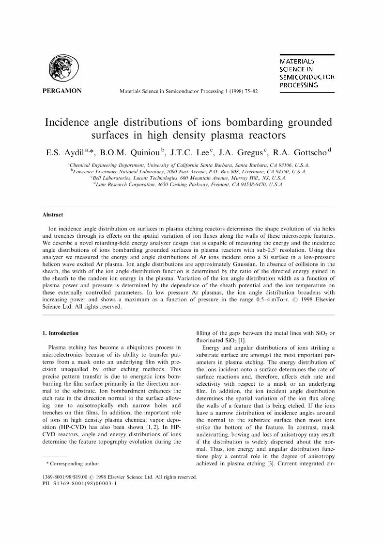
The experiments were conducted in the downstreamregion of a high density helicon wave excited plasma
Fig. 1. Schematic of the helicon plasma source, the plasma reactor, and the di�erentially pumped chamber that houses the ion
energy and angle distribution measurement apparatus.
E. Aydil et al. / Materials Science in Semiconductor Processing 1 (1998) 75±8276
shown schematically in Fig. 1. The plasma reactor
chamber was the same one that was previously used
for studying ion and metastable atom transport in the
source and reactor regions of electron cyclotron reson-
ance and helicon-wave driven discharges [17±21]. The
plasma chamber was pumped by a 1500 l secÿ1 Turbo
molecular pump and had a base pressure of 10ÿ7 Torr.
The pressure in the chamber was measured by capaci-
tance manometers but not actively controlled. The Ar
¯ow rate was regulated using a mass ¯ow controller
and fed into the reactor from the top of a quartz tube
that, along with the helicon antenna, forms the plasma
source. The plasma was maintained in the quartz tube
by applying radio frequency (RF) power at 13.56 MHz
to a helicon antenna through a matching network. The
plasma expands from the quartz tube, the source
region, into a stainless steel vacuum chamber referred
to as the reactor region. The wafers would normally be
placed on a substrate platen in the reactor region,
facing the plasma expanding from the source.
For the ion energy and angle distribution measure-
ments, a hollow di�erentially pumped chamber
replaced the substrate platen of the reactor described
above. The top surface of this chamber played the role
of the substrate platen. Fig. 2 shows a detailed sche-
matic of the di�erentially pumped chamber and the
retarding-®eld energy and angle distribution analyzer
housed in this chamber. The ions incident onto the
substrate plane are sampled through a single circular
via hole that connects the plasma chamber to the dif-
ferentially pumped analysis chamber. The via holes
used in this study were 50 mm in diameter and were
produced on 35 mm thick, 5 mm � 5 mm square Si
membranes on 20 mm � 20 mm Si dies. The Si dies
Fig. 2. Schematic of the retarding-®eld energy analyzer and the position sensitive detector for simultaneous measurement of the ion
energy and angle distribution functions.
E. Aydil et al. / Materials Science in Semiconductor Processing 1 (1998) 75±82 77
with the sampling hole were placed into a recessed
groove on the center of the sample platen and
mechanically clamped to ensure good thermal contact.
Circulating cooling water through a channel recessed
into the substrate platen cooled the membranes. The
pressure in the di�erentially pumped chamber was
maintained at 10ÿ7 Torr to eliminate ion collision with
gas molecules after they have passed through the
sampling hole. In fact, both the plasma chamber (0.5±
5 mTorr) and the analysis chamber pressure are low
enough that the ion motion is essentially collisionless
from the time they enter the platen sheath to the time
they are detected.
Ion energies are analyzed using a retarding grid ana-
lyzer that consists of four hemispherical grids and two
¯at grids in the stacking con®guration shown in Fig. 2.
The top grid, labeled grid 1, is equipotential with the
substrate platen and both of them are grounded to cre-
ate a ®eld free region immediately below the sampling
hole. Grids 2 and 3 are biased at a positive potential
and used to discriminate and repel the ions that have
energies below the potential applied to grid 3, Vr. Two
grids are used to provide a smooth repulsive barrier
and to improve the energy resolution of the ionizer.
Grid 2 is biased at a potential aVr where a < 1. Grids
4 and 5 are maintained at the same potential to pro-
vide a ®eld free region between the ¯at grids and the
hemispherical grids. Grid 6 is biased at a negative po-
tential to repel the electrons sampled through the hole
with the ions. After grid 6, the ions are accelerated
towards a microchannel plate detector (MCP) placed
7 cm from the sampling hole. Since the distance
between grids 5 and 6 and grid 5 and the MCP detec-
tor are very small compared to the distance between
the sampling hole and the detector, the change in the
trajectory of the ions between grids 5 and 6 is very
small. Each ion striking the top of the MCP detector
creates a localized electron avalanche that travels
through the channels of the MCP. Thus the MCP
ampli®es the ion current while preserving the infor-
mation about where the ion struck the MCP surface.
The electrons emerging from the opposite end of the
MCP detector are accelerated towards a phosphorus
coated plate and excite phosphorescence at the same
location that the original ion hit the MCP detector. A
CCD camera placed outside the vacuum records the
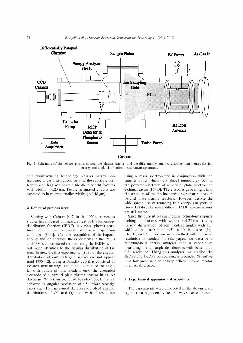
Fig. 3. A typical recorded and digitized image of the ions hitting the phosphorus plate. The plasma is maintained at 2 mTorr with
0.5 kW of RF power. The retarding potential, Vr is 12 V. The line drawn through the center is a typical section used to obtain the
averaged distributions shown in Fig. 5. Many such lines were drawn through the center of the image at di�erent polar angles to
obtain the ion incidence angle distributions.
E. Aydil et al. / Materials Science in Semiconductor Processing 1 (1998) 75±8278
phosphorescence image through a lens. This imagingmethod provides a projection of the locations of the
ions striking the MCP detector. The ion incidenceangle with respect to the normal to the platen surface
is related to the ion impingement location on the MCP
through simple geometry. Since the brightness at a par-ticular location on the image is proportional to the
time averaged ¯ux of the ions striking the MCP, an
image recorded with the ion retarding potential set atVr is the energy averaged ion angle distribution func-
tions from eVr to in®nity. The quantitative ion angle
distribution functions are determined by grabbing,digitizing and analyzing the image. The locations with
respect to the pinhole and size of the image are cali-
brated using an alignment cross, patterned onto thephosphorus screen.
A conservative estimate of the analyzer's angular
resolution shows that it is <0.58. We estimate that thedeviation introduced to the ion trajectory between
grids 5 and the MCP detector is 08 when y = 08 and
ÿ0.38 when y= 58, increasing with increasing y.Another source of loss of resolution is the smearing of
the ion incidence location due to cross talk between
the MCP channels, which were 0.25 mm in diameter.However, this e�ect is negligible compared to other
sources of error. A typical spatial resolution of 0.1 mm
on the MCP detector translates into an uncertainty<0.18 in the incidence angles of the detected ions.
Finally, a resolution loss is incurred when the imagecreated on the phosphorus screen is pixelized and digi-
tized. Typical images consisted of 128 � 128 pixels that
spanned an area that was ca 5 cm � 5 cm. Thus, asingle pixel represents a signal averaged over a 0.38angle. Based, on these calculations we estimate that
this analyzer has a resolution better than 0.58.Unfortunately, determining the true resolution requires
an ion source that can produce ions with angular dis-
tribution widths <0.58 and such a source is not readilyavailable.
4. Experimental results
Fig. 3 shows a typical image of the ions striking theMCP detector as projected onto the phosphorus screen
and recorded by the CCD camera. The image wasrecorded while maintaining an Ar plasma at 2 mTorr
with 0.5 kW of RF power. The retarding potential was
set at 12 V to repel all ions that have energies <12 V.Under the conditions of the experiment in Fig. 3,
almost all the ions have energies above 12 V. Thus the
image represents the energy integrated angular distri-butions of ions passing through the hole. Except for
small ¯uctuations in the brightness as a function of the
position on the detector, the images appeared axisym-metric with respect to the polar angle, f, of a coordi-
nate system on the detector plane whose origin is the
projection of the pinhole onto this plane. While thereis no reason to expect the images to be axisymmetric
we chose to focus on distributions with respect to the
ion incidence angle, y, by averaging intensities alongmany di�erent lines drawn through the center of the
bright spot, at di�erent polar angles, f, as shown in
Fig. 3. In principle, imperfections in the via hole walls,as well as di�erential charging of the feature sidewalls
can produce asymmetries in the ion angle distribution
observed below the hole. Such e�ects should even bemore pronounced if the via hole has a high aspect
ratio. In fact, the high ion ¯ux sensitivity and resol-
ution of this technique allows one to study such subtlee�ects as distortion of ion angle and energy distri-
bution functions by the feature. Herein, we limit our
study to features with low aspect ratio (0.7). In thelimit that the aspect ratio approaches zero and the
hole diameter is on the order of or smaller than theDebye length, one obtains the angle and energy distri-
butions incident onto the substrate surface. These con-
ditions are satis®ed in our studies where the Debyelength 20±50 mm is on the same order as the sampling
hole diameter (50 mm).
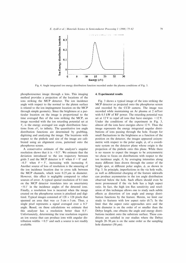
Fig. 4. Angle integrated ion energy distribution function recorded under the plasma conditions of Fig. 3.
E. Aydil et al. / Materials Science in Semiconductor Processing 1 (1998) 75±82 79
Fig. 4 displays the energy distribution function of
the ions imaged in Fig. 3. The maximum ion energy is
17 V indicating that this value is also the maximum
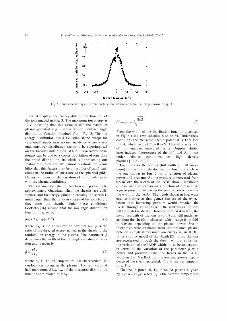
plasma potential. Fig. 5 shows the ion incidence angle
distribution function obtained from Fig. 3. The ion
energy distribution has a Gaussian shape except for
very small angles near normal incidence where a sec-
ond, narrower distribution seems to be superimposed
on the broader distribution. While this narrower com-
ponent can be due to a cooler population of ions than
the broad distribution, its width is approaching our
spatial resolution and we cannot overlook the possi-
bility that this feature may be an artifact of small vari-
ations in the radius of curvature of the spherical grids.
Herein, we focus on the variation of the broader peak
with the plasma conditions.
The ion angle distribution function is expected to be
approximately Guassian, when the sheaths are colli-
sionless and the energy gained in crossing the sheath is
much larger than the random energy of the ions before
they enter the sheath. Under these conditions,
Gottscho [16] showed that the ion angle distribution
function is given by
f�y�1CN exp�ÿby2� �1�where CN is the normalization constant and b is the
ratio of the directed energy gained in the sheath to the
random ion energy in the plasma. The parameter bdetermines the width of the ion angle distribution func-
tion and is given by
b � eVs
kT��2�
where T+ is the ion temperature that characterizes the
random ion energy in the plasma. The full width at
half maximum, DyFWHM, of the measured distribution
functions are related to b by
DyFWHM � 2
��������ln 2
b
s�3�
From the width of the distribution function displayedin Fig. 4 (10.48) we calculate b to be 84. Under these
conditions the measured sheath potential is 17 V (seeFig. 4) which yields kT+=0.2 eV. This value is typical
of ion energies measured using Doppler shiftedlaser induced ¯uorescence of the N+
2 and Ar+ ions
under similar conditions in high density
plasmas [19, 20, 22, 23].Fig. 6 shows the widths (full width at half maxi-
mum) of the ion angle distribution functions such asthe one shown in Fig. 5, as a function of plasma
power and pressure. As the pressure is increased from
0.5 mTorr, the widths of the IADF show a maximumca 2 mTorr and decrease as a function of pressure. At
a given pressure, increasing the plasma power increasesthe width of the IADF. The trends shown in Fig. 6 are
counterintuitive at ®rst glance because of the expec-tation that increasing pressure would broaden the
IADF through collisions with the neutrals as the ions
fall through the sheath. However, even at 4 mTorr, themean free path of the ions is ca 0.8 cm, still much lar-
ger than the sheath thicknesses, which range from 0.01to 0.05 cm depending on the plasma power. Sheath
thicknesses were estimated from the measured plasmapotentials (highest measured ion energy in an IEDF)
using a simple model of the sheath [24]. Since the ionsare accelerated through the sheath without collisions,
the variation of the IADF widths must be understood
in terms of the variation of the parameter b withpower and pressure. Thus, the trends in the IADF
width in Fig. 6 re¯ect the pressure and power depen-dence of the sheath potential, Vs and the ion tempera-
ture, T+.
The sheath potential, Vs, in an Ar plasma is givenby Vs=4.7 kTe/e, where Te is the electron temperature
Fig. 5. Ion incidence angle distribution function determined from the image shown in Fig. 3.
E. Aydil et al. / Materials Science in Semiconductor Processing 1 (1998) 75±8280
and k is the Boltzmann constant. A simple balancebetween the ion production by ionization and loss by
recombination on the walls yields [25, 26]
ki�Te�������������������kTe=M�
p � 1
NL�4�
where N is the neutral density, L is the reactor charac-
teristic length and ki is the ionization rate constant. Ifthe dependence of the ionization rate constant on the
electron temperature is known this equation can besolved to yield an estimate of the average electron tem-
perature in the plasma. In an Ar plasma, the electron
temperature and the plasma potential decrease withincreasing neutral density. The dependence of the ion
temperature on the neutral density and power is com-plex but, in general, the ion temperature increases with
power and decreases with neutral density as chargeexchange and other collisions with neutrals cool the
ions. Since both the numerator and the denominator
of the parameter b decreases with neutral density, thedependence of the IADF width is determined by the
details of how Vp and T+ vary with decreasing N. Thesituation is complicated by the fact that signi®cant gas
heating may also a�ect the neutral density at constantpressure [27], and pressure, measured at a single point
downstream from the discharge, may not be represen-
tative of the gas density in the reactor. Furthermore,in high-density plasmas, the neutral density may be a
function of position in the reactor [28, 29]. All thesecomplications preclude simple explanation and predic-
tion of the behavior of the IADF widths with changingpower and pressure. Nevertheless, one can still under-
stand some of the changes in Fig. 6 in terms of
changes in b with variations in power and pressure.Simple but relatively accurate models of the plasma
predict that the electron temperature and the plasmapotential are independent of power. Thus, the increasein the width of the IADF with increasing power is
attributed to increased ion heating and higher T+.Hotter ion temperature at high RF power is either dueto more intense ®elds in the plasma or due to
decreased N and mean free path between collisions: atconstant pressure, gas heating would result in a neutraldensity decrease. If one ignores gas heating and
assumes that the neutral density is approximately pro-portional to the pressure, the general decreasing trendin the IADF with increasing pressure can be under-stood in terms of T+ decreasing faster (a 1/N) than Vp
which decreases approximately logarithmically (a lnN). However, this mechanism alone does not explainthe maximum in the IADF width at 2 mTorr.
Sophisticated models that take into account the detailsof ion creation, heating and transport in high densityplasma reactors are needed to fully understand the
changes displayed in Fig. 6.
5. Summary, conclusions and future work
In summary, we have designed and built an appar-atus that is capable of measuring the ion energy and
incidence angle distributions bombarding surfaces inplasma reactors with unprecedented resolution. Theapparatus was used to determine the ion angle distri-
butions incident onto a grounded surface placed in thedownstream of a helicon wave excited high densityplasma source. The ion angle distributions were ap-
proximately Guassian and the width of the distributionfunction depends on power and pressure. In absence ofcollisions in the sheath, the ratio of the directed energy
Fig. 6. Full width at half maximum of the ion energy distribution function as a function of pressure and power.
E. Aydil et al. / Materials Science in Semiconductor Processing 1 (1998) 75±82 81
gained in the sheath to the thermal energy of the ionsin the plasma determines the IADF widths.
In practical etching and deposition processes, thesubstrate is biased with RF power. The methoddescribed herein can be extended to measurements of
the IEDF and IADF incident onto rf-biased substrateelectrodes. To accomplish this, the d.c. potentialsapplied to the various components of the analyzer
must be with respect to the RF potential on the sub-strate electrode, using the electrode potential as a vir-tual ground. A method for accomplishing this and the
electronics will be described in a future publication [30].The data provided herein should be helpful in validat-ing plasma simulation models that can predict ionangle distributions as a function of externally con-
trolled plasma parameters such as power and pressure.
Acknowledgements
This work was performed as a part of a Cooperative
Research and Development Agreement between BellLaboratories and Lawrence Livermore Laboratories.The authors acknowledge fruitful discussions with Drs
Dale Ibbotson of Lucent Technologies and NormanBardsley of Lawrence Livermore Laboratories. E. A.also acknowledges funding from the National ScienceFoundation through a National Young Investigator
Award (ECS9457758). We would like to thank ErikEdelberg and Sang Han for their help in the prep-aration of the manuscript.
References
[1] Shu�ebotham MWP, Pirkle D, Denison D. Mater. Sci.
Forum 1993;255:140±2.
[2] Han SM, Aydil ES. J. Vac. Sci. Technol. A
1996;14:2062.
[3] Gottscho RA, Jurgensen CW, Vitkavage DJ. J. Vac. Sci.
Technol. B 1992;10:2133.
[4] Coburn JW. Rev. Sci. Instrum. 1970;41:1219.
[5] Coburn JW, Kay E. J. Appl. Phys 1972;43:4965.
[6] Kohler K, Coburn JW, Horne DE, Kay E, Keller JH. J.
Appl. Phys 1985;57:5966.
[7] Coburn JW. Thin Solid Films 1989;171:65.
[8] Bohm C, Perrin J. Rev. Sci. Instrum. 1993;64:31.
[9] Ingram SG, Braithwaite NSJ. J. Phys. D: Appl. Phys.
1988;21:1496.
[10] Manenschijn A, Jansses GCAM, Van der Drift E,
Radelaar S. J. Appl. Phys. 1991;69:1253.
[11] Thompson BE, Allen KD, Richards AD, Sawin HH. J.
Appl. Phys. 1986;59:1890.
[12] Liu J, Huppert GL, Sawin HH. J. Appl. Phys.
1990;68:3916.
[13] Janes J, Huth C. J. Vac. Sci. Technol. A 1992;10:3522.
[14] Janes J, Huth C. J. Vac. Sci. Technol. A 1992;10:3086.
[15] Janes J, Huth C. Appl. Phys. Lett. 1992;61:261.
[16] Gottscho RA. J. Vac. Sci. Technol. 1993;11:1884.
[17] Giapis KP, Sadeghi N, Margot J, Gottscho RA, Lee
TCJ. J. Appl. Phys. 1993;73:7188.
[18] Nakano T, Sadeghi N, Gottscho RA. Appl. Phys. Lett.
1991;58:458.
[19] Nakano T, Sadeghi N, Trevor DJ, Gottscho RA,
Boswell RW. J. Appl. Phys. 1992;72:3384.
[20] Sadeghi N, Nakano T, Trevor DJ, Gottscho RA. J.
Appl. Phys. 1991;70:2552.
[21] Trevor DJ, Sadeghi N, Nakano T, Derouard J, Gottscho
RA, Foo PD, Cook JM. Appl. Phys. Lett. 1990;57:1188.
[22] Hartog EAD, Persing H, Woods RC. Appl. Phys. Lett.
1990;57:661.
[23] Wood RC, McClain RL, Mahoney LJ, Hartog EAD,
Persing H, Hamers JS. SPIE 1991;1594:366.
[24] Economou DJ, Evans DR, Alkire RC. J. Electrochem.
Soc. 1988;135:756.
[25] Lieberman, M.A., Lichtenberg, A.J.. Principles of
Plasma Discharges and Materials Processing. New York: