Page 1
Increasing Adder Efficiency by Exploiting Input
Statistics
by
Andrew Lawrence Clough
Submitted to the Department of Electrical Engineering and ComputerScience
in partial fulfillment of the requirements for the degree of
Master of Engineering in Computer Science and Electrical Engineering
at the
MASSACHUSETTS INSTITUTE OF TECHNOLOGY
June 2007
c© Andrew Lawrence Clough, MMVII. All rights reserved.
The author hereby grants to MIT permission to reproduce anddistribute publicly paper and electronic copies of this thesis document
in whole or in part.
Author . . . . . . . . . . . . . . . . . . . . . . . . . . . . . . . . . . . . . . . . . . . . . . . . . . . . . . . . . . . . . .Department of Electrical Engineering and Computer Science
May 10, 2007
Certified by. . . . . . . . . . . . . . . . . . . . . . . . . . . . . . . . . . . . . . . . . . . . . . . . . . . . . . . . . .Vladimir StojanovicAssistant ProfessorThesis Supervisor
Accepted by . . . . . . . . . . . . . . . . . . . . . . . . . . . . . . . . . . . . . . . . . . . . . . . . . . . . . . . . .Arthur C. Smith
Chairman, Department Committee on Graduate Students
Page 3
Increasing Adder Efficiency by Exploiting Input Statistics
by
Andrew Lawrence Clough
Submitted to the Department of Electrical Engineering and Computer Scienceon May 10, 2007, in partial fulfillment of the
requirements for the degree ofMaster of Engineering in Computer Science and Electrical Engineering
Abstract
Current techniques for characterizing the power consumption of adders rely on as-suming that the inputs are completely random. However, the inputs generated byrealistic applications are not random, and in fact include a great deal of structure.Input bits are more likely to remain in the same logical states from addition to addi-tion than would be expected by chance and bits, especially the most significant bits,are very likely to be in the same state as their neighbors.
Taking this data, I look at ways that it can be used to improve the design ofadders. The first method I look at involves looking at how different adder architecturesrespond to the different characteristics of input data from the more significant andless significant bits of the adder, and trying to use these responses to create a hybridadder. Unfortunately the differences are not sufficient for this approach to be effective.I next look at the implications of the data I collected for the optimization of Kogge-Stone adder trees, and find that in certain circumstances the use of experimentallyderived activity maps rather than ones based on simple assumptions can increaseadder performance by as much as 30%.
Thesis Supervisor: Vladimir StojanovicTitle: Assistant Professor
3
Page 5
Acknowledgments
I would like to thank Professor Stojanovic for all his help, advice, patience, and for
giving me the opportunity to work on this thesis.
Thank you to Chris Batten for introducing me to Pin. I am sure collecting the
data I needed would have been far more difficult without that wonderful tool.
I would like to thank the people at SIPB for their help with my questions about
Unix and C++ programming on Athena.
Finally, thank you to my parents for their support and encouragement.
5
Page 7
Contents
1 Introduction 13
1.1 Importance . . . . . . . . . . . . . . . . . . . . . . . . . . . . . . . . 13
1.2 Existing Techniques . . . . . . . . . . . . . . . . . . . . . . . . . . . . 14
1.2.1 Constant Activity Factor . . . . . . . . . . . . . . . . . . . . . 14
1.2.2 Simulation . . . . . . . . . . . . . . . . . . . . . . . . . . . . . 14
1.3 Thesis Plan . . . . . . . . . . . . . . . . . . . . . . . . . . . . . . . . 15
1.3.1 Experimentation and Observation . . . . . . . . . . . . . . . . 15
1.3.2 Design and Testing . . . . . . . . . . . . . . . . . . . . . . . . 16
2 PIN 17
2.1 How PIN Works . . . . . . . . . . . . . . . . . . . . . . . . . . . . . . 17
2.2 Using PIN . . . . . . . . . . . . . . . . . . . . . . . . . . . . . . . . . 18
2.2.1 Sample Choice . . . . . . . . . . . . . . . . . . . . . . . . . . 18
2.2.2 Extracting Additions . . . . . . . . . . . . . . . . . . . . . . . 18
2.2.3 Analysis . . . . . . . . . . . . . . . . . . . . . . . . . . . . . . 19
2.2.4 Data . . . . . . . . . . . . . . . . . . . . . . . . . . . . . . . . 19
3 Characteristics of Adder Inputs 21
3.1 Number Size . . . . . . . . . . . . . . . . . . . . . . . . . . . . . . . . 21
3.2 Auto-Correlation . . . . . . . . . . . . . . . . . . . . . . . . . . . . . 22
3.3 Input Activity Factors . . . . . . . . . . . . . . . . . . . . . . . . . . 24
3.4 Neighbor Correlation . . . . . . . . . . . . . . . . . . . . . . . . . . . 24
3.5 Relative Frequency of Ones and Zeros . . . . . . . . . . . . . . . . . . 27
7
Page 8
3.6 Generate Frequency . . . . . . . . . . . . . . . . . . . . . . . . . . . . 28
3.7 Propagate Frequency . . . . . . . . . . . . . . . . . . . . . . . . . . . 29
3.8 Carry Frequency . . . . . . . . . . . . . . . . . . . . . . . . . . . . . 30
4 Hybrid Architectures 31
4.1 Goals . . . . . . . . . . . . . . . . . . . . . . . . . . . . . . . . . . . . 31
4.2 Adders . . . . . . . . . . . . . . . . . . . . . . . . . . . . . . . . . . . 32
4.2.1 Pass Ripple . . . . . . . . . . . . . . . . . . . . . . . . . . . . 32
4.2.2 Mirror Ripple . . . . . . . . . . . . . . . . . . . . . . . . . . . 34
4.2.3 Carry Bypass . . . . . . . . . . . . . . . . . . . . . . . . . . . 35
4.2.4 Carry Select . . . . . . . . . . . . . . . . . . . . . . . . . . . . 36
4.2.5 Han-Carlson . . . . . . . . . . . . . . . . . . . . . . . . . . . . 37
4.3 Comparison . . . . . . . . . . . . . . . . . . . . . . . . . . . . . . . . 38
5 Improvements in Kogge-Stone Gate Sizing 41
5.1 Previous Work . . . . . . . . . . . . . . . . . . . . . . . . . . . . . . 41
5.2 Changes and New Work . . . . . . . . . . . . . . . . . . . . . . . . . 43
5.3 Results . . . . . . . . . . . . . . . . . . . . . . . . . . . . . . . . . . . 46
8
Page 9
List of Figures
3-1 Number of occurences of different sized adder inputs . . . . . . . . . 22
3-2 Auto-Correlation of inputs between subsequent additions . . . . . . . 23
3-3 Activity factor for the inputs . . . . . . . . . . . . . . . . . . . . . . . 24
3-4 Cross-Correlation Between Neighboring Bits . . . . . . . . . . . . . . 25
3-5 % of additions where a given bit is a one . . . . . . . . . . . . . . . . 27
3-6 % of additions where a given bit is in the generate state . . . . . . . . 28
3-7 % of additions where a given bit is in the propagate state . . . . . . . 29
3-8 % of additions where a given bit has a carry out . . . . . . . . . . . . 30
4-1 Pass Logic . . . . . . . . . . . . . . . . . . . . . . . . . . . . . . . . . 33
4-2 Ripple Adder . . . . . . . . . . . . . . . . . . . . . . . . . . . . . . . 33
4-3 Mirror Logic . . . . . . . . . . . . . . . . . . . . . . . . . . . . . . . . 34
4-4 Carry Bypass Architecture . . . . . . . . . . . . . . . . . . . . . . . . 35
4-5 Carry Select Architecture . . . . . . . . . . . . . . . . . . . . . . . . 36
4-6 Han-Carlson Architecture . . . . . . . . . . . . . . . . . . . . . . . . 37
4-7 Han-Carlson Architecture . . . . . . . . . . . . . . . . . . . . . . . . 38
5-1 Kogge-Stone Architecture . . . . . . . . . . . . . . . . . . . . . . . . 42
5-2 Results of Power Optimizations with Bernoulli Inputs . . . . . . . . . 42
5-3 Changes in P Activity . . . . . . . . . . . . . . . . . . . . . . . . . . 43
5-4 Changes in G Activity . . . . . . . . . . . . . . . . . . . . . . . . . . 44
5-5 Results of Power Optimizations with Observed Inputs . . . . . . . . . 45
5-6 Energy Use Differences for Vd, Vt, and W optimization . . . . . . . . 46
5-7 Energy Use Differences for Vd, Vt, and W optimization . . . . . . . . 47
9
Page 11
List of Tables
4.1 Adder Performance Comparison . . . . . . . . . . . . . . . . . . . . . 38
4.2 Adder Energy Use by Segment . . . . . . . . . . . . . . . . . . . . . . 39
11
Page 13
Chapter 1
Introduction
1.1 Importance
Managing power consumption is an aspect of microprocessor design that is important
and growing increasingly more so. In mobile electronics reducing power consumption
is a key factor in increasing battery life, and even in servers and desktop computers
power dissipation is an important design constraint.
In any form of engineering there are inevitably tradeoffs to be made, and one of
the primary tradeoffs facing designers is that of trying to balance performance against
power dissipation. Through choices in such factors as voltage levels, microarchitec-
ture, logic style, or gate sizing a designer can make tradeoffs between the two, and
seek to find the balance that will best fit the designer’s goals.
To make these choices designers require information about the consequences of
their decisions, and circuit designers use models of varying accuracy and speed to
help them forsee the consequences of their choices. An accurate understanding of the
causes and severity of the power dissipation within a chip might influence a designer
to make certain tradeoffs between speed and power, but a less accurate understanding
might lead to tradeoffs that are worse for overall performance. Clearly an accurate
representation of how a microchip dissipates power is instrumental to good design.
Circuit activity is generally one of the most important factors in energy dissipation.
In this thesis I will be looking at adders specifically, and experimentally determine
13
Page 14
activity factors. From there, I examine how these vary from standard models and
how this variance effects design choices.
1.2 Existing Techniques
1.2.1 Constant Activity Factor
The most common means of determining the power dissipation of a circuit is to assume
some constant switching activity factor for all the gates in the circuit, and then use
that to determine the overall power use of that section of the circuit. The formula
following formula is commonly used.
Ptotal = pt(CL · V · Vdd · fclk) + ISC · Vdd + Ileakage · Vdd
Here the first term represents the power consumed by switching activity and the
second represents the short circuit power loss and the third represents the power lost
due to leakage. In the first term pt represents the activity factor, CL represents the
loading capacitance, V is the swing voltage, Vdd is the supply voltage, and fclk is
the clock frequency. In the second term ISC represents the short-circuit current that
occurs when the adder is in an intermediate state and in the third Ileakage represents
the leakage current.
The value for pt is generally found by using rules of thumb, such as assuming a
15% activity factor for gates in static adders and a 50% activity factor for gates in
dynamic adders [10], while the other variables can be determined more precisely.
1.2.2 Simulation
A more sophisticated approach to power estimation involves simulating the circuit
block in question for some set of inputs. It is ordinarily quite time consuming to
run enough input vectors to be sure that the results are sufficiently accurate, but
there are many ways to speed up or approximate the process that can be used if the
experimenter assumes that the inputs to the adder are statistically independent of
14
Page 15
each other, and more that can be used if the additional assumption that the inputs
are are Bernoulli processes is also used [3].
These assumptions and approximations are generally used, and with adders it is
generally assumed by designers that each input is a Bernoulli Process with each input
having an equal chance of being either a one or a zero independent of its neighbors
or of previous samples [7] [9].
Once the activity factors of the various gates have been determined, the same
equation as in the constant activity factor method can be used to estimate power
consumption.
1.3 Thesis Plan
1.3.1 Experimentation and Observation
It is clear that the structure of the inputs to an adder is more complicated than either
of these two methods can represent. When a program is run some types of inputs to
the adder such as memory addresses approximate Bernoulli inputs. However, more
often one or both of the inputs will be considerably smaller than the 32 or 64 bit
width of the adder input. Sometimes, as with basic control loops, both of the inputs
to the adder will be much less than the the entire adder width and sometimes, as
with memory addressing in an array, only one of the two inputs will be small. Even
when one of the inputs fills the entire width of the adder there will be cases in which
it will tend to remain the same or change very little from addition to addition causing
another sort of statistical structure in the activity factors.
To quantify the distributions and correlations of the various inputs I used a pro-
gram called PIN [5] that allows me to look at the values of numbers being added
together while a program is being executed. In Chapter 2 I discuss how PIN works
and how I used it to gether my data, while in Chapter 3 I discuss the results of my
observations.
15
Page 16
1.3.2 Design and Testing
After gathering my data, I pursued two approaches in how to use this data for im-
proving adder designs.
The first approach, discussed in Chapter 4, is to look at the possibility of using
different architectures to exploit the statistical differences between the most significant
bits of the input and the least significant. Unfortunately this method did not lead to
any significant improvements.
The second approach, discussed in Chapter 5, is to look at how more accurate
activity models can be used to improve previous optimizations [2][8] for a Han Carlson
adder. I look at optimizations based upon the data I collected and optimizations based
upon Bernoulli inputs, and compare them. This method is more fruitful, and does
seem to yield useful results though more research is necessary.
16
Page 17
Chapter 2
PIN
2.1 How PIN Works
Pin is a tool that takes programs and dynamically instruments it, essentially taking
an executable and inserting arbitrary code at any point. Pin runs under Linux on
Intel Xscale, IA-32, IA-32E, and Itanium processors.
When a program begins running under Pin, Pin starts by taking a sequence of
instructions bounded by branches and rewrites them adding new code according to
the specifications of the user. When the branch is reached, Pin rewrites the next
sequence from the branch target and the original program continues. So that the
behavior of the original program won’t be unintentionally changed Pin restores any
registers that have been overwritten by the injected code after that code has finished
executing. All the generated code is kept in memory so that it can be reused.
Pintools written by the user to govern the behavior of PIN. They contain the code
which PIN inserts into the target program and specify the conditions under which it is
inserted. These pintools are written in C++ and compiled using libraries distributed
along with Pin.
17
Page 18
2.2 Using PIN
2.2.1 Sample Choice
In order to make sure that any patterns discovered are not the artifacts of a single
program but rather patterns that tend to appear in most normal processor opera-
tion I used a cross-section of five programs to collect data from. The five were a
simple program to list the contents of a directory (ls), an mp3 player (mpg123), a
PDF viewer (GPdf), a math processing program (MATLAB), and a web browser
(Mozilla).
2.2.2 Extracting Additions
The two pintools used for analysis and for data collection inspect the use of the adder
in the same way. Whenever PIN sees that an instruction using the adder is about
to be executed, it injects a piece of code to read the operands of the addition. The
instructions that make use of the adder are as follows:
ADD The values of the two operands are simply added together and the result is
saved.
ADC The values of the two operands are added together, as well as the carry flag,
and the result is saved.
XADD Exchanges the locations of the two operands, then adds them.
INC Adds 1 to the operand and saves the result.
SUB Adds one operand and the two’s complement of the other, and then saves the
result.
SBB Adds one operand and the two’s complement of the other as well as the carry
bit, and then saves the result.
CMP Adds one operand to the two’s complement of the other, but does not save
the result and merely sets status flags.
18
Page 19
DEC Adds the two’s complement of 1 to the operand and saves the result.
When the pintool finds one of these instructions, it checks whether the operands
are stored as constants in the instruction, in registers, or in memory. Before the
instruction is executed, the pintool reads the values of the operands, applies two’s
complement as necessary, and sends the results to the analysis function. In the case
of an INC or DEC a 1 or two’s complement -1 is fed to the analysis function as the
second operand.
2.2.3 Analysis
The analysis pintool I used works by taking each set of adder inputs and making
a series of comparisons both within the inputs themselves and between them and
the previous set of inputs. The results of these will later be used to determine the
correlations between various aspects of the inputs. However, the pintool also runs a
simulation to determine, for a ripple carry adder with these inputs, what percentage
of the time each bit would be in a generate or propagate state, as well as what the
carry activity looks like.
2.2.4 Data
The data collection pintools record the actual sequence of inputs to the adder so that
the optimizations in sections 4 and 5 can be tested. Both optimizations are tested
with 10,000 sample additions from each of the five sample programs. Each set of
inputs is broken up into 100 equally sized regions and blocks of 100 additions are
randomly selected from within each region.
Different pintools were used depending on the program being sampled. Because ls
and mpg123 use a relatively small number of additions in their operation the pintool
that extracts the data from them records every input. Since the number of additions
preformed by each sample program is known after it has finished running they can
be broken into regions and the block selected when the pintool output is converted
to a form that can be used by other programs.
19
Page 20
Since GPdf, MATLAB, and Mozilla all use a relatively large number of addi-
tions, the time and storage space required to save every adder input for the entire
run would be prohibitive. Because of this I created a second pintool that assumed
100,000,000 overall additions and region sizes of 1,000,000, and only saved the ran-
domly selected block from each region. Since all three of the programs could be run
for variable lengths of time, each could be run to 100,000,000 additions and then
terminated.
20
Page 21
Chapter 3
Characteristics of Adder Inputs
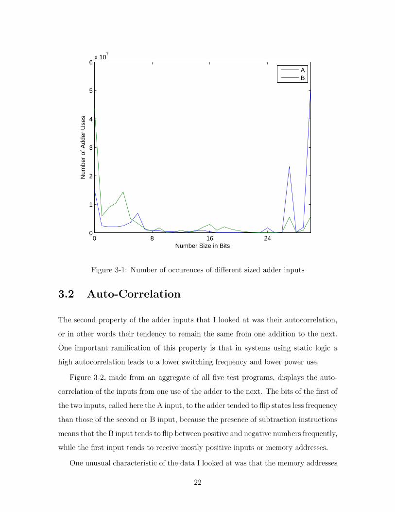
3.1 Number Size
Among the properties of the adder inputs that I examined, the first I looked at was the
distribution of number sizes entering the adder. Under a two’s complement system
such as is used by most microprocessors today, finding the size of a number is a matter
of finding the most significant bit in the number which doesn’t match the sign bit.
Many of the additions were clustered into two spikes at the upper end of the range.
It was a property of the computer used to run the sample programs that many of the
memory addresses used by it began with either 10111 or 00001, resulting in two large
spikes indicating those two numbers.
Benford’s Law [1] tells us that in many real world situations we can expect the
frequency with which a number occurs to be proportional to the inverse of the size of
the number or in other words that numbers are distributed evenly on a logarithmic
scale. The data from PIN seem to roughly match this distribution, though again
idiosyncracies in various programs prevent the distribution from matching Benford’s
distribution precisely.
21
Page 22
0 8 16 240
1
2
3
4
5
6x 10
7
Number Size in Bits
Num
ber
of A
dder
Use
s
AB
Figure 3-1: Number of occurences of different sized adder inputs
3.2 Auto-Correlation
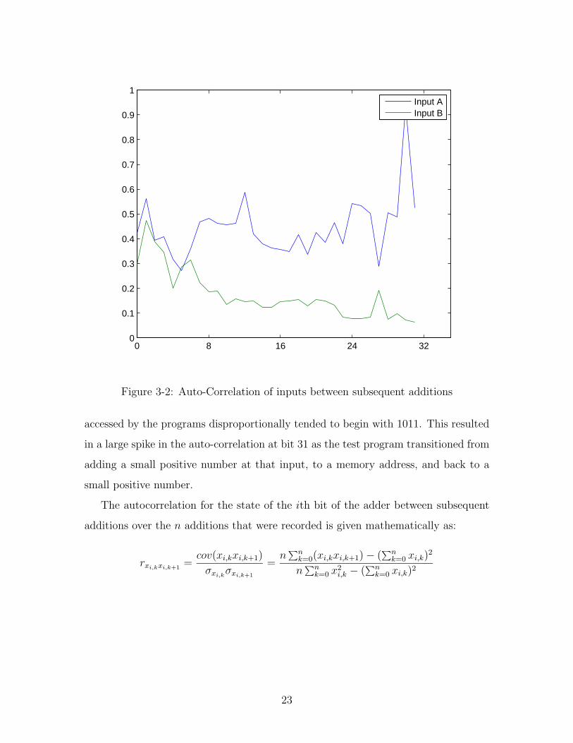
The second property of the adder inputs that I looked at was their autocorrelation,
or in other words their tendency to remain the same from one addition to the next.
One important ramification of this property is that in systems using static logic a
high autocorrelation leads to a lower switching frequency and lower power use.
Figure 3-2, made from an aggregate of all five test programs, displays the auto-
correlation of the inputs from one use of the adder to the next. The bits of the first of
the two inputs, called here the A input, to the adder tended to flip states less frequency
than those of the second or B input, because the presence of subtraction instructions
means that the B input tends to flip between positive and negative numbers frequently,
while the first input tends to receive mostly positive inputs or memory addresses.
One unusual characteristic of the data I looked at was that the memory addresses
22
Page 23
0 8 16 24 320
0.1
0.2
0.3
0.4
0.5
0.6
0.7
0.8
0.9
1
Input AInput B
Figure 3-2: Auto-Correlation of inputs between subsequent additions
accessed by the programs disproportionally tended to begin with 1011. This resulted
in a large spike in the auto-correlation at bit 31 as the test program transitioned from
adding a small positive number at that input, to a memory address, and back to a
small positive number.
The autocorrelation for the state of the ith bit of the adder between subsequent
additions over the n additions that were recorded is given mathematically as:
rxi,kxi,k+1=
cov(xi,kxi,k+1)
σxi,kσxi,k+1
=n
∑nk=0(xi,kxi,k+1) − (
∑nk=0 xi,k)
2
n∑n
k=0 x2i,k − (
∑nk=0 xi,k)2
23
Page 24
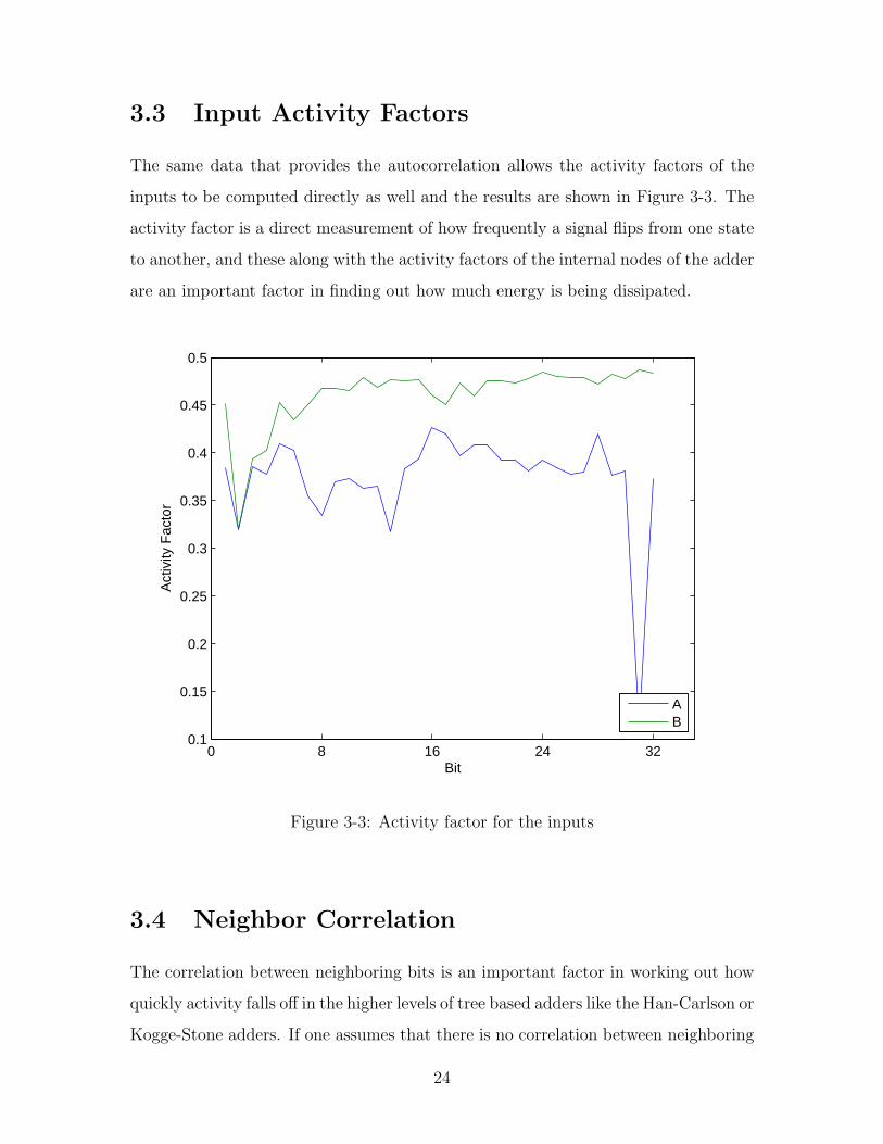
3.3 Input Activity Factors
The same data that provides the autocorrelation allows the activity factors of the
inputs to be computed directly as well and the results are shown in Figure 3-3. The
activity factor is a direct measurement of how frequently a signal flips from one state
to another, and these along with the activity factors of the internal nodes of the adder
are an important factor in finding out how much energy is being dissipated.
0 8 16 24 320.1
0.15
0.2
0.25
0.3
0.35
0.4
0.45
0.5
Bit
Act
ivity
Fac
tor
AB
Figure 3-3: Activity factor for the inputs
3.4 Neighbor Correlation
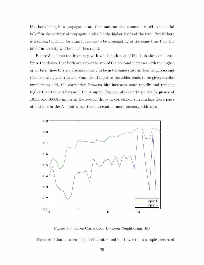
The correlation between neighboring bits is an important factor in working out how
quickly activity falls off in the higher levels of tree based adders like the Han-Carlson or
Kogge-Stone adders. If one assumes that there is no correlation between neighboring
24
Page 25
bits both being in a propagate state then one can also assume a rapid exponential
falloff in the activity of propagate nodes for the higher levels of the tree. But if there
is a strong tendency for adjacent nodes to be propagating at the same time then the
falloff in activity will be much less rapid.
Figure 3-4 shows the frequency with which each pair of bits is in the same state.
Since the chance that both are above the size of the operand increases with the higher
order bits, these bits are also more likely to be in the same state as their neighbors and
thus be strongly correlated. Since the B input to the adder tends to be given smaller
numbers to add, the correlation between bits increases more rapidly and remains
higher than the correlation in the A input. One can also clearly see the frequency of
10111 and 000010 inputs in the sudden drops in correlation surrounding those pairs
of odd bits in the A input which tends to contain more memory addresses.
0 8 16 240.1
0.2
0.3
0.4
0.5
0.6
0.7
0.8
0.9
Input AInput B
Figure 3-4: Cross-Correlation Between Neighboring Bits
The correlation between neighboring bits i and i + 1 over the n samples recorded
25
Page 26
is calculated with the following equation:
rxi,kxi+1,k=
cov(xi,kxi+1,k)
σxi,kσxi+1,k
=n
∑nk=0(xi,kxi+1,k) −
∑nk=0 xi,k
∑nk=0 xi+1,k
√
n∑n
k=0 x2i,k − (
∑nk=0 xi,k)2
√
n∑n
k=0 x2i+1,k − (
∑nk=0 xi+1,k)2
26
Page 27
3.5 Relative Frequency of Ones and Zeros
0 8 16 24 320.05
0.1
0.15
0.2
0.25
0.3
0.35
0.4
0.45
0.5
AB
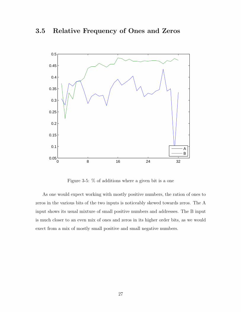
Figure 3-5: % of additions where a given bit is a one
As one would expect working with mostly positive numbers, the ration of ones to
zeros in the various bits of the two inputs is noticeably skewed towards zeros. The A
input shows its usual mixture of small positive numbers and addresses. The B input
is much closer to an even mix of ones and zeros in its higher order bits, as we would
exect from a mix of mostly small positive and small negative numbers.
27
Page 28
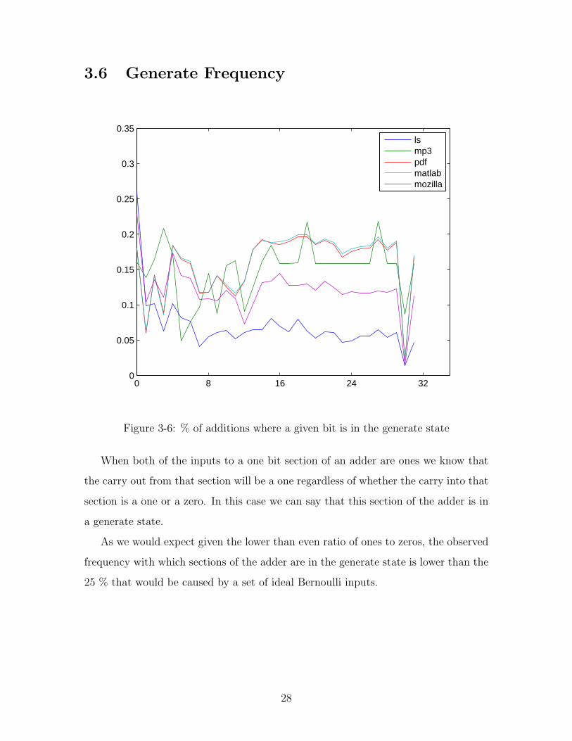
3.6 Generate Frequency
0 8 16 24 320
0.05
0.1
0.15
0.2
0.25
0.3
0.35
lsmp3pdfmatlabmozilla
Figure 3-6: % of additions where a given bit is in the generate state
When both of the inputs to a one bit section of an adder are ones we know that
the carry out from that section will be a one regardless of whether the carry into that
section is a one or a zero. In this case we can say that this section of the adder is in
a generate state.
As we would expect given the lower than even ratio of ones to zeros, the observed
frequency with which sections of the adder are in the generate state is lower than the
25 % that would be caused by a set of ideal Bernoulli inputs.
28
Page 29
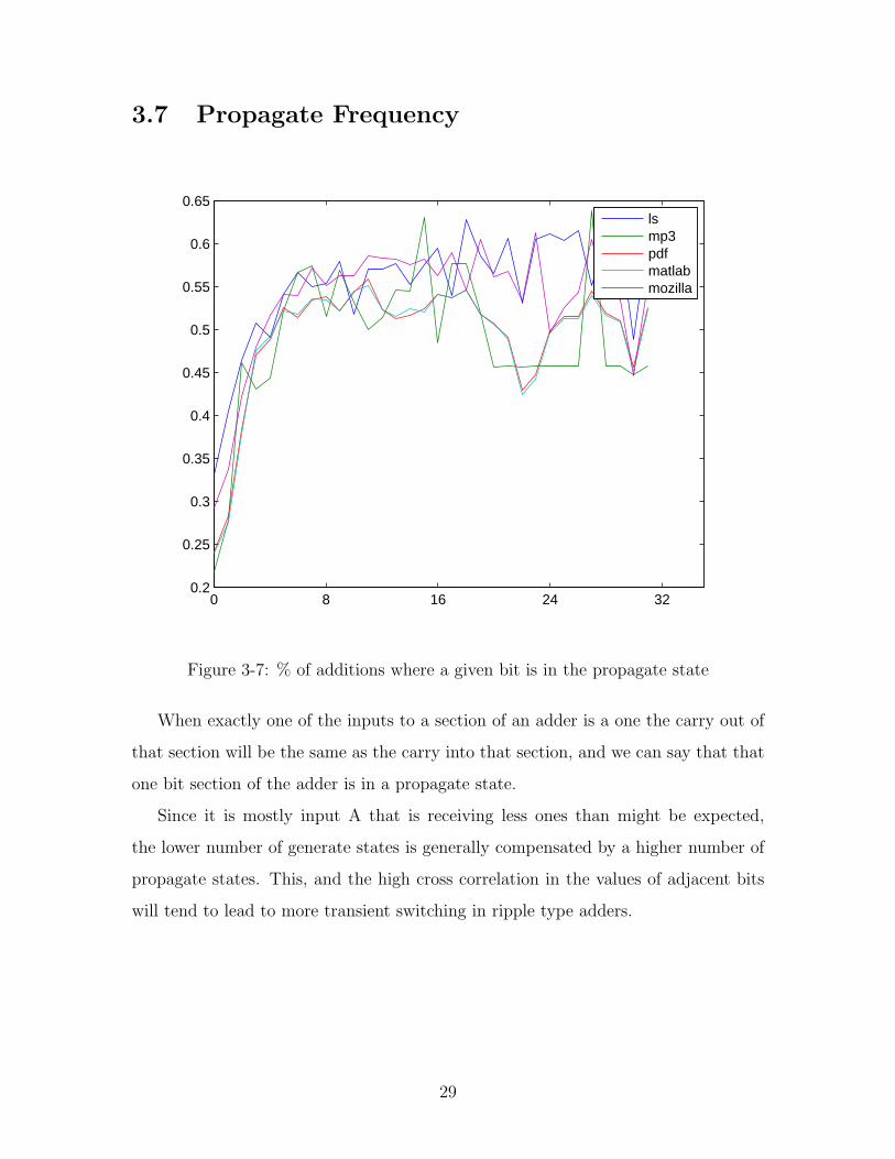
3.7 Propagate Frequency
0 8 16 24 320.2
0.25
0.3
0.35
0.4
0.45
0.5
0.55
0.6
0.65
lsmp3pdfmatlabmozilla
Figure 3-7: % of additions where a given bit is in the propagate state
When exactly one of the inputs to a section of an adder is a one the carry out of
that section will be the same as the carry into that section, and we can say that that
one bit section of the adder is in a propagate state.
Since it is mostly input A that is receiving less ones than might be expected,
the lower number of generate states is generally compensated by a higher number of
propagate states. This, and the high cross correlation in the values of adjacent bits
will tend to lead to more transient switching in ripple type adders.
29
Page 30
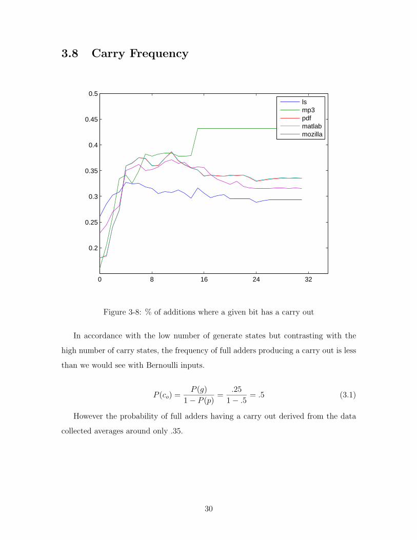
3.8 Carry Frequency
0 8 16 24 32
0.2
0.25
0.3
0.35
0.4
0.45
0.5
lsmp3pdfmatlabmozilla
Figure 3-8: % of additions where a given bit has a carry out
In accordance with the low number of generate states but contrasting with the
high number of carry states, the frequency of full adders producing a carry out is less
than we would see with Bernoulli inputs.
P (co) =P (g)
1 − P (p)=
.25
1 − .5= .5 (3.1)
However the probability of full adders having a carry out derived from the data
collected averages around only .35.
30
Page 31
Chapter 4
Hybrid Architectures
4.1 Goals
My work in Chapter 3 revealed substantial differences in statistical behavior between
bits in the upper and lower reaches of the adder. In this chapter I look first at
the effect of these differences on the energy use of different sections of an adder for
different architectures. Then I use that information to try to create a hybrid adder
using different architectures in the sections of the adder that are best suited to them
in order to improve overall efficiency.
For example, assume adder A used three quarters of its energy in bits 0-15 while
adder B used equal amounts of energy in bits 0-15 and bits 16-31. If adders A and
B both have the same energy-delay product and if they can be combined so that the
delay of a hybrid adder is the mean of the delays of each individually, then replacing
the first 16 bits of adder A with the logic from adder B will yield an adder with
an energy-delay product 25 % smaller than that of its component adders. If the
distribution of energy use within two adders differs sharply enough it would even
be useful to combine two adders with different energy-delay products, or two adders
whose delays don’t add linearly.
31
Page 32
4.2 Adders
I examined five different types of adders, a pass logic based ripple adder, a mirror
ripple adder, a carry-skip adder, a carry-select adder, and a Han-Carlson tree adder.
I simulated each in Spice with BSIM3 V3.1 [6] using the data collected from PIN as
inputs and record the energy used by each type. So as not to allow different levels of
optimization skew the results the widths of the gates are kept small for each design
except in cases of large fanout, and they were all built using 250nm technology at
2.5V.
4.2.1 Pass Ripple
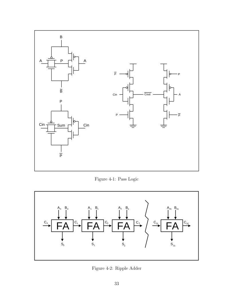
This adder uses elements that are a combination of NMOS pass logic and standard
CMOS logic. Not shown in Figure 4-1 are the CMOS inverters required to create the
inverted inputs to the Xor gates. The 32 bit adder that was simulated was made by
stringing together 32 of these elements as shown in Figure 4-2.
32
Page 33
AA
B
B
P
CinCin
P
P
Sum
CoutCin
P
P P
P
A
Figure 4-1: Pass Logic
FA
A B
S
C
FA
A B
S
C
FA
A B
S
C
FA
A B
S
C
0
0
0
10 2
1
11
2
2 2
2 31
31
31 31
C C32
Figure 4-2: Ripple Adder
33
Page 34
A B B
A
B
B
C i
A
A
B B
A
A
C i
C i
C i
C i
B
B
A
A
CO S
Figure 4-3: Mirror Logic
4.2.2 Mirror Ripple
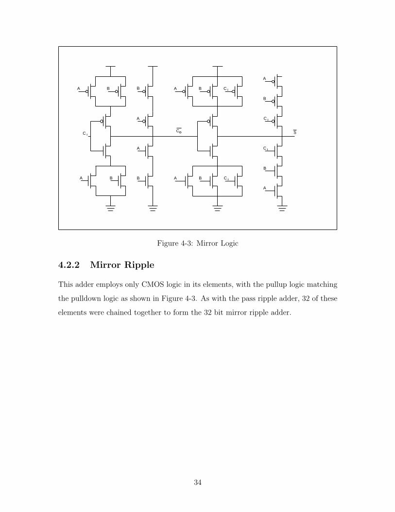
This adder employs only CMOS logic in its elements, with the pullup logic matching
the pulldown logic as shown in Figure 4-3. As with the pass ripple adder, 32 of these
elements were chained together to form the 32 bit mirror ripple adder.
34
Page 35
FA FA
Carry Propagate
Setup
Sum
Bits 2-3Bits 0-1
Carry Propagate
Setup
Sum
Bits 4-6
Carry Propagate
Setup
Sum
Bits 7-10
Carry Propagate
Setup
Sum
Bits 11-15
Carry Propagate
Setup
Sum
Bits 16-20
Carry Propagate
Setup
Sum
Bits 21-24
Carry Propagate
Setup
Sum
Bits 25-27
Carry Propagate
Setup
Sum
Bits 28-30
FA FA
Bits 30-31
Figure 4-4: Carry Bypass Architecture
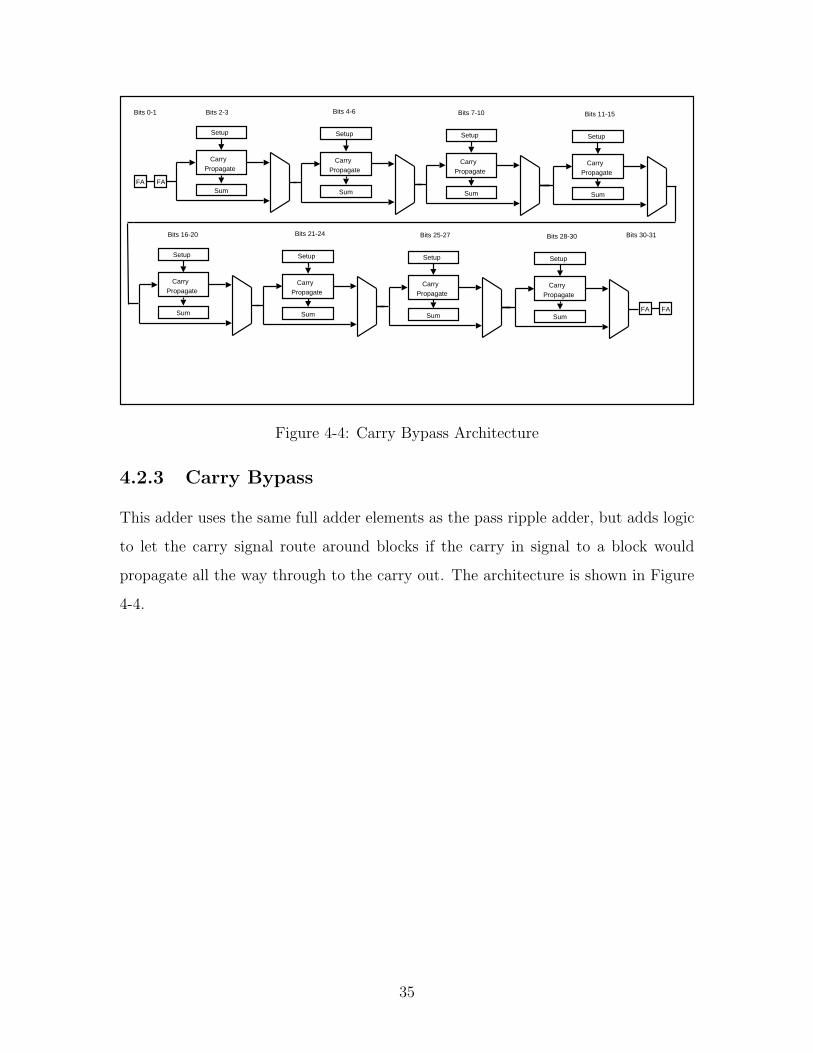
4.2.3 Carry Bypass
This adder uses the same full adder elements as the pass ripple adder, but adds logic
to let the carry signal route around blocks if the carry in signal to a block would
propagate all the way through to the carry out. The architecture is shown in Figure
4-4.
35
Page 36
FA FA
Bits 2-3Bits 0-1
FA FA
FA FA
"0"
"1"
Select
Bits 4-6
"0" Carry
"1" Carry
Select
Bits 7-10
"0" Carry
"1" Carry
Select
Bits 11-16
"0" Carry
"1" Carry
Select
Bits 17-23
"0" Carry
"1" Carry
Select
Bits 24-31
"0" Carry
"1" Carry
Select
Figure 4-5: Carry Select Architecture
4.2.4 Carry Select
A Carry Select Adder, shown in Figure 4-5, consists of a number of blocks each of
which run a pair of ripple adder chains in parallel. One chain is fed a ’1’ as its first
carry-in, and the other is fed a ’0’. The carry output of the previous block is then
used to select the set of outputs from one of the two chains.
36
Page 37
A ,B0 0
S0
A ,B1 1
S1
A ,B2 2
S2
A ,B3 3
S3
A ,B4 4
S4
A ,B5 5
S5
A ,B6 6
S6
A ,B7 7
S7
A ,B8 8
S8
A ,B9 9
S9
A ,B10 10
S10
A ,B11 11
S11
A ,B12 12
S12
A ,B13 13
S13
A ,B14 14
S14
A ,B15 15
S15
Figure 4-6: Han-Carlson Architecture
4.2.5 Han-Carlson
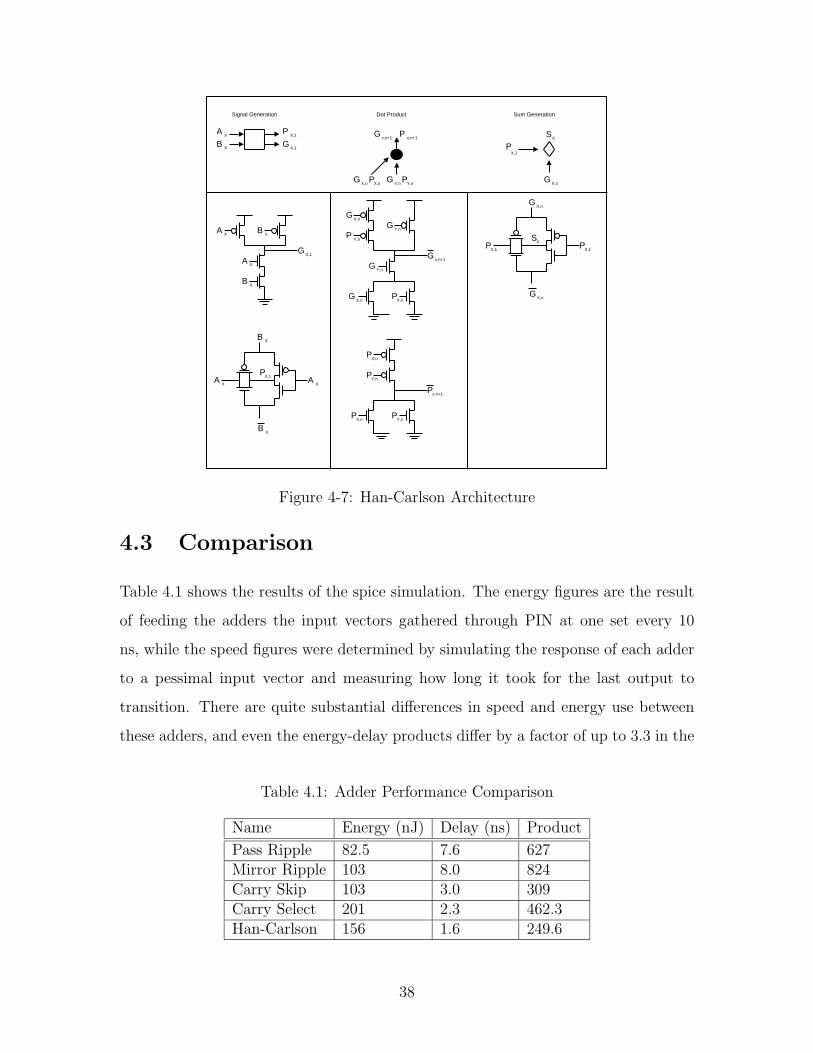
The Han-Carlson adder is a member of the tree adder family of adders. Using sev-
eral layers of logic, it computes the carry states across blocks that increase in size
exponentially as the signal travels up the layers. Shown below in Figure 4-6 is a 16
bit variant of this class of adder. The actual adder used in simulations was 32 bits
wide and had one extra layer. There are three different of circuit elements used in
the architecture which are shown in Figure 4-7.
37
Page 38
X SX
A
XB
Signal Generation
PX,1
GX,1
XA
XA
XB
XB
X,1G
XB
XB
XA
XA
PX,1
PX,n
GX,n
PY,n
GY,n
Px,n+1
Gx,n+1
Dot Product
X,nG
Y,nG
Y,nG
X,nG
x,n+1G
Y,nP
X,nP
X,nP
Y,nP
X,nP
Y,nP
x,n+1P
GX,n
PX,1
X,nG
X,nG
X,1P
X,1P
SX
Sum Generation
Figure 4-7: Han-Carlson Architecture
4.3 Comparison
Table 4.1 shows the results of the spice simulation. The energy figures are the result
of feeding the adders the input vectors gathered through PIN at one set every 10
ns, while the speed figures were determined by simulating the response of each adder
to a pessimal input vector and measuring how long it took for the last output to
transition. There are quite substantial differences in speed and energy use between
these adders, and even the energy-delay products differ by a factor of up to 3.3 in the
Table 4.1: Adder Performance Comparison
Name Energy (nJ) Delay (ns) Product
Pass Ripple 82.5 7.6 627Mirror Ripple 103 8.0 824Carry Skip 103 3.0 309Carry Select 201 2.3 462.3Han-Carlson 156 1.6 249.6
38
Page 39
Table 4.2: Adder Energy Use by Segment
Name Energy in Bits 0-15 Energy in Bits 16-31 Ratio
Pass Ripple 40.81 39.82 1.025Mirror Ripple 52.62 50.08 1.051Carry Skip 52.08 50.62 1.029Carry Select 99.56 101.32 .9826Han-Carlson 75.87 78.56 .9658
case of the mirror ripple adder compared to the Han-Carlson adder.
Any succesful hybrid would have to be made from two adders that use different
amounts of energy in their high and low order bits. Looking at energy use for different
sectors of the adders, from least significant to most.
As can be seen, the differences between the different halves of the adders are
relatively small. These differences in the distribution of energy use are small enough
that the gains achieved by any hybrid making use of them would be drowned out
by differences in energy-delay product and by situations where the delays cannot be
averaged together linearly.
39
Page 41
Chapter 5
Improvements in Kogge-Stone
Gate Sizing
5.1 Previous Work
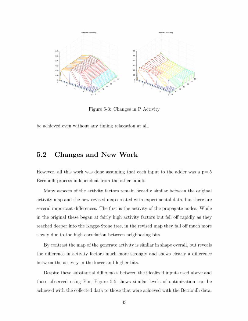
This method of optimization draws heavily from and uses tools developed for the true
power optimization work of Markovic, Stojanovic, Nikolic, Horowitz, and Brodersen[2][8].
The section of their work adapted in this thesis was their analysis of ways to trade
off the supply voltage (Vdd), threshold voltage (Vtt), and sizing (W ) to create more
energy efficient designs.
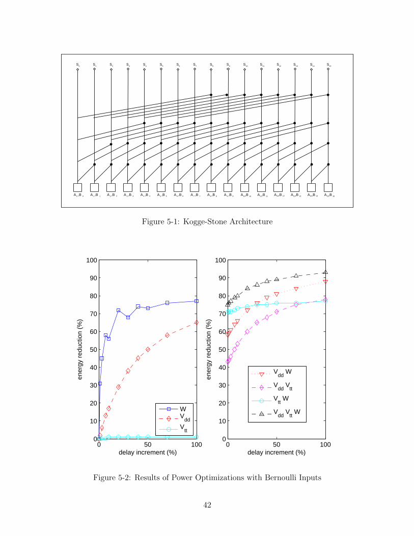
Using a Kogge-Stone adder, similar to the Han-Carlson and depicted in Figure
5-1, they first designed one with gate sizes optimized for speed and using the nominal
supply voltages and threshold voltages for the technology. Relevant to this thesis,
they looked at two things.
For a baseline, they took the timing figure for the optimized adder, relaxed it to
some extent, and then developed methods to optimize for minimum energy while still
meeting that timing by altering the supply, threshold, or sizing. For Vdd and W even
relatively small relaxations in timing could cause large drops in energy.
Additionally, they used a similar technique to optimize for minimum energy while
trading off two, or all three of the variables. Because the supply and threshold voltages
had not been previously optimized for the situation, substantial energy savings could
41
Page 42
A ,B0 0
S0
A ,B1 1
S1
A ,B2 2
S2
A ,B3 3
S3
A ,B4 4
S4
A ,B5 5
S5
A ,B6 6
S6
A ,B7 7
S7
A ,B8 8
S8
A ,B9 9
S9
A ,B10 10
S10
A ,B11 11
S11
A ,B12 12
S12
A ,B13 13
S13
A ,B14 14
S14
A ,B15 15
S15
Figure 5-1: Kogge-Stone Architecture
0 50 1000
10
20
30
40
50
60
70
80
90
100
delay increment (%)
ener
gy r
educ
tion
(%)
WV
ddV
tt
0 50 1000
10
20
30
40
50
60
70
80
90
100
delay increment (%)
ener
gy r
educ
tion
(%)
Vdd
W
Vdd
Vtt
Vtt W
Vdd
Vtt W
Figure 5-2: Results of Power Optimizations with Bernoulli Inputs
42
Page 43
1
2
3
4
5 05
1015
2025
300
0.1
0.2
0.3
0.4
0.5
0.6
Origonal P Activity
1
2
3
4
5 05
1015
2025
300
0.1
0.2
0.3
0.4
0.5
0.6
Revised P Activity
Figure 5-3: Changes in P Activity
be achieved even without any timing relaxation at all.
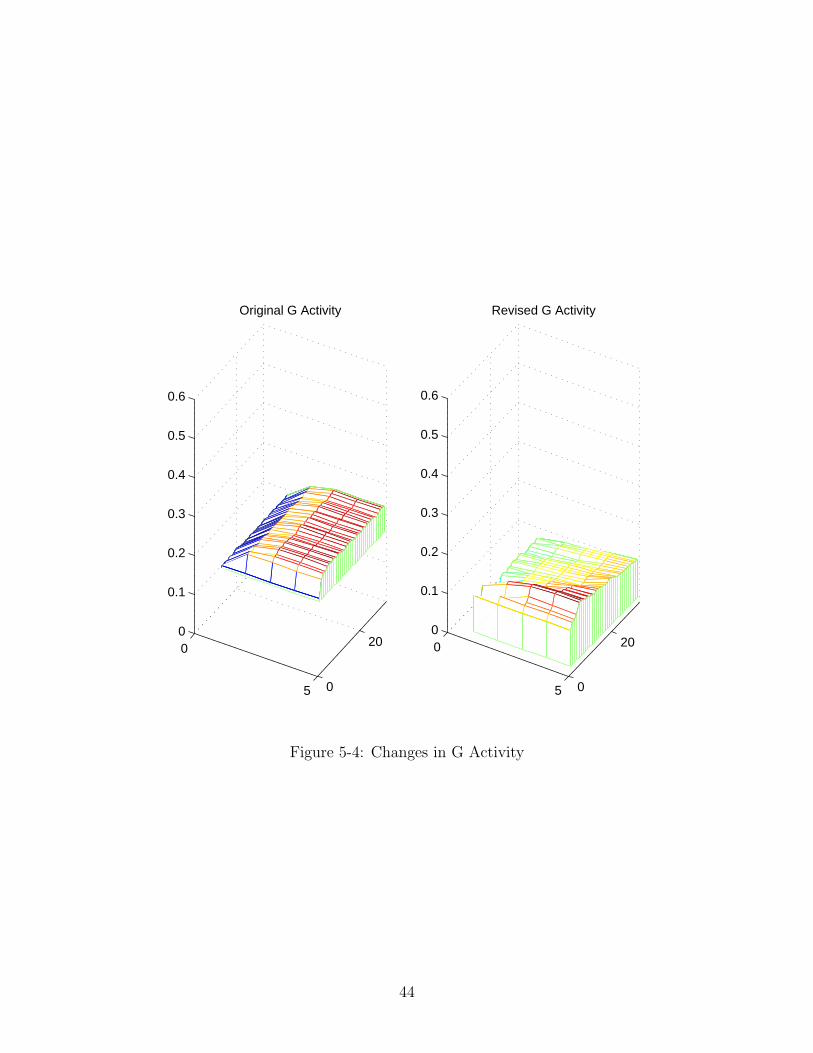
5.2 Changes and New Work
However, all this work was done assuming that each input to the adder was a p=.5
Bernoulli process independent from the other inputs.
Many aspects of the activity factors remain broadly similar between the original
activity map and the new revised map created with experimental data, but there are
several important differences. The first is the activity of the propagate nodes. While
in the original these began at fairly high activity factors but fell off rapidly as they
reached deeper into the Kogge-Stone tree, in the revised map they fall off much more
slowly due to the high correlation between neighboring bits.
By contrast the map of the generate activity is similar in shape overall, but reveals
the difference in activity factors much more strongly and shows clearly a difference
between the activity in the lower and higher bits.
Despite these substantial differences between the idealized inputs used above and
those observed using Pin, Figure 5-5 shows similar levels of optimization can be
achieved with the collected data to those that were achieved with the Bernoulli data.
43
Page 44
0
5 0
200
0.1
0.2
0.3
0.4
0.5
0.6
Original G Activity
0
5 0
200
0.1
0.2
0.3
0.4
0.5
0.6
Revised G Activity
Figure 5-4: Changes in G Activity
44
Page 45
0 50 1000
10
20
30
40
50
60
70
80
90
100
delay increment (%)
ener
gy r
educ
tion
(%)
WV
ddV
tt
0 50 1000
10
20
30
40
50
60
70
80
90
100
delay increment (%)
ener
gy r
educ
tion
(%)
Vdd
W
Vdd
Vtt
Vtt W
Vdd
Vtt W
Figure 5-5: Results of Power Optimizations with Observed Inputs
45
Page 46
0 10 20 30 40 50 60 70 80 90 1000
100
200
300
400
500
600
700
800
900
1000
Delay Increment (%)
Ene
rgy
Use
d
old optimization with origonal map
old optimization with new map
new optimization with new map
new optimization with old map
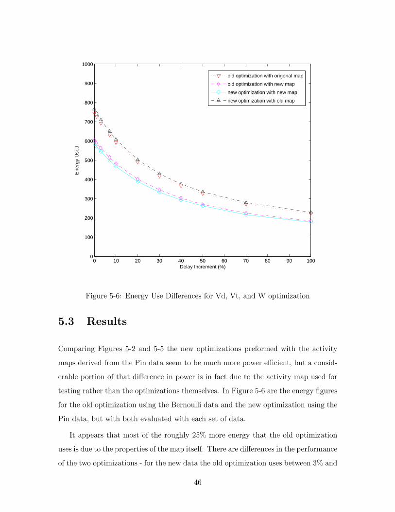
Figure 5-6: Energy Use Differences for Vd, Vt, and W optimization
5.3 Results
Comparing Figures 5-2 and 5-5 the new optimizations preformed with the activity
maps derived from the Pin data seem to be much more power efficient, but a consid-
erable portion of that difference in power is in fact due to the activity map used for
testing rather than the optimizations themselves. In Figure 5-6 are the energy figures
for the old optimization using the Bernoulli data and the new optimization using the
Pin data, but with both evaluated with each set of data.
It appears that most of the roughly 25% more energy that the old optimization
uses is due to the properties of the map itself. There are differences in the performance
of the two optimizations - for the new data the old optimization uses between 3% and
46
Page 47
0 50 1000
100
200
300
400
500
600
700
800
900
1000
Delay Increment (%)
Ene
rgy
Use
d
0 5 100
10
20
30
40
50
60
70
80
90
100
Del
ay In
crem
ent D
ecre
ase
(%)
Sample Point
new map
old map
Figure 5-7: Energy Use Differences for Vd, Vt, and W optimization
3.5% more energy while for the old data the new optimization uses between 2.5% and
3% more energy. The differences between the maps themselves explain the majority
of the difference, however.
Using the correct activity map may have a relatively small effect on the optimiza-
tion itself but if a designer finds themselves facing a hard limit in terms of average
power dissipation the use of the Pin derived activity maps might still result in signif-
icant performance gains.
For a given power target the difference between the delay required by the old data
and the delay allowed by the new can vary from 10% to 30%, a far more significant
difference.
47
Page 49
Bibliography
[1] Frank Benford. The law of anomalous numbers. Proceedings of the American
Philosophical Society, 1938.
[2] Robert W. Brodersen, Mark A. Horowitz, Dejan Markovic, Borivoje Nikolic,
and Vladimir Stojanovic. Methods for true power minimization. IEEE/ACM
International Converence on Computer Aided Design, 2002.
[3] R. Burch, F. Najm, R. Yang, and T. Trick. A monte carlo approach for power
estimation. IEEE Transactions on VLSI Systems, 1(1):8, March 1993.
[4] A.P. Chandrakasan, S. Sheng, and R.W. Brodersen. Low-power cmos digital
design. IEEE Transactions on Circuits and Systems, 38(8):10, August 1990.
[5] Chi-Keung Luk Robert Cohn, Robert Muth, Harish Patil, Artur Klauser, Ge-
off Lowney, Steven Wallace, Vijay Janapa Reddi, and Kim Hazelwood. Pin:
Building customized program analysis tools with dynamic instrumentation. Pro-
ceedings of PLDI, 2005.
[6] http://www-device.eecs.berkeley.edu/b̃sim3/arch ftp.html.
[7] P. Landman and J. Rabaey. Architectural power analysis: The dual bit type
method. IEEE Transactions on Very Large Scale Integration (VLSI) Systems,
3(2), June 1995.
[8] Dejan Markovic, Vladimir Stojanovic, Borivoje Nikolic, Mark A. Horowitz, and
Robert W. Brodersen. Methods for true energy-performance optimization. IEEE
Journal of Solid-State Circuits, 39(8):12, August 2004.
49
Page 50
[9] F.N. Najm. A survey of power estimation techniques in vlsi circuits. 2(4):10,
December 1994.
[10] Vojin G. Oklobdzija, Bart R. Zeydel, Hoang Q. Dao Sanu Mathew, and Ram
Krishnamurthy. Comparison of high-peformance vlsi adders in the energy delay
space. IEEE Transactions on Very Large Scale Integration (VLSI) Systems,
13(6):5, June 2005.
[11] V. Tiwari, S. Malik, and A. Wolfe. Power analysis of embedded sfotware: A first
step towards software power minimization. 2(4):9, December 1994.
50