Page 1
Indian Institutes and Fermi lab
Collaboration (IIFC) for project X
Development of 325 MHz Solid-State RF
Power Amplifiers for Project X,
under Addendum-V of IIFC
Manjiri Pande and Team
@ RFSS, IADD, BARC,INDIA
July 19, 2012
under Addendum-V of IIFC
Page 2
� The solid-state radio frequency (RF) power amplifier has several advantages
over the tube amplifiers. These are mainly,
� At BARC, we have been working on Radio Frequency (RF) systems for various
scientific applications including accelerator. Simultaneously, as a technology
development program, BARC had started design and development of ‘Solid
State RF Amplifiers‘ So, it was decided to continue our work under the
collaboration for project X also.
Manjiri/RFSS/IADD/Physics Group/BARC/IndiaJuly 19, 2012
• High reliability,
• Simple start-up procedure
• Graceful power degradation
• Easy maintenance
• Low voltage operation
• Simpler cooling requirements
• Use of low power circulators.
Page 3
• Deliverables under the collaboration
A. 1 kW, 325 MHz, solid state power amplifier (SSPA)A. 1 kW, 325 MHz, solid state power amplifier (SSPA)
B. 3 kW, 325 MHz, solid state power amplifier (SSPA)
C. 7 kW, 325 MHz, solid state power amplifier (SSPA)
July 19, 2012Manjiri/RFSS/IADD/Physics Group/BARC/India
/
Page 4
SSPA
A solid state power amplifier (SSPA) comprises of:
1. SMPS DC power supplies
2. Driver amplifier
3. RF amplifier modules
4. Input splitter
5. Output combiner
6. Directional Coupler
7. Interlocking & protection circuit
July 19, 2012Manjiri/RFSS/IADD/Physics Group/BARC/India
Page 5
Architecture of SSRFPA
Po
we
r sp
litte
r
po
we
r co
mb
ine
r
PA
PA n
Directional
coupler
n
Control
Signal
RF
Load
RF
signal
Driver
Po
we
r sp
litte
r
po
we
r co
mb
ine
r
PA
1P
A
1
Compact DC supplies Interlock and Protection Water cooling
RF
Switch
July 19, 2012
Load
Manjiri/RFSS/IADD/Physics Group/BARC/India
Page 6
Initially, we started with technology development of the most
important basic building blocks of SSPA, i.e.
1) High efficiency RF amplifier power modules (1 kW) and1) High efficiency RF amplifier power modules (1 kW) and
2) Power combiner /divider technology at various power levels.
July 19, 2012 Manjiri/RFSS/IADD/Physics Group/BARC
Page 7
RF module 300 W at 350 MHz
Initial development of SSPA
Manjiri / RFSS/IADD/Physics Group/BARC/ IndiaJuly 19, 2012
Initially, as a part of technology development, a basic 300 Watt RF
module at 350 MHz was developed.
Four such modules were developed and combined to develop 1.1 kW
RF amplifier
Another eight such modules were developed and combined to develop
2.1 kW RF amplifier.
Page 8
Then, 325 MHz, 1 kW Amplifier modules has been designed.
Substantial investigation was done using different laminates
based on their properties like dielectric strength, thermal
conductivity etc.
SSPA
RFPAs were developed in three types of printed circuit boards
(pcb) material (laminates) as,
a) FR4
b) Ceramic filled PTFE and
c) Glass microfiber reinforced PTFE
July 19, 2012 Manjiri/RFSS/IADD/Physics Group/BARC/India
Page 9
A) 1 kW, 325 MHz SSPA: Test results
a) 325 MHz Amplifier- FR4 –Single module: Results:
Short time test (1/2 hr) : 1 kW
Long term test (8 hrs) : 800 W
Power gain (1 dB) : 19.5 dB
Overall Efficiency : 68 %
Manjiri / RFSS/IADD/Physics Group/BARC/indiaJuly 19, 2012
RF module 1000 W at 325 MHz
Page 10
• As a first prototype, two such FR4 boards, each board operating
at 600 W were combined.
Test Results
1. Power: 600 W /module
2. 2 modules of 600 W each and are
A)a) 1 kW, 325 MHz SSPA - FR4 – combined – Test set up
2. 2 modules of 600 W each and are
combined
3. 2-way micro strip combiner
4. Overall power gain: 19.8 dB
5. Ptotal:1.04 kW
6. Efficiency (DC/RF) : 62.7 %
Manjiri / RFSS/IADD/Physics Group/BARC/India
Combined RF system under test
July 19, 2012
Page 11
These two tested FR4 boards are now housed back to back on one single water
cooled heat sink and in one single rack along with all other associated
components like,
1. SMPS DC power supplies
2. Driver amplifier
3. RF modules
4. Input splitter
5. Output combiner
A)1) 1 kW, 325 MHz SSPA
5. Output combiner
6. Directional Coupler
7.Interlocking & protection circuit
Size: 19” 6U rack
This total RF system has been tested with the following parameters :
1. Po: 1005 watt
2. Efficiency (DC/RF): 65.26 %
3. Combined Gain (2 modules): 19.28 (dB)
4. Efficiency (AC/RF): 58.05 %
Manjiri / RFSS/IADD/Physics Group/BARC/IndiaJuly 19, 2012
Page 12
A) b) 325 MHz Amplifier- ceramic filled PTFE laminate
based board
Another RF module based on ceramic
filled PTFE laminate was designed,
developed and tested.
Test results of 1 kW RF module
1. Center frequency : 325 MHz
2. Power output (CW) (max.) : 915 W2. Power output (CW) (max.) : 915 W
3. Power output (CW) (typ.) : 893 W
4. Gain (typ.) : 22.8 dB
5. Cooling : Water Cooled
6. Efficiency (DC/RF)(PAE): 71.04 %
7. Efficiency (AC/RF) : 63.94 %
Manjiri / RFSS/IADD/Physics Group/BARC/IndiaJuly 19, 2012
1 kW RF module test set up
Page 13
SSPA
• Now, two such boards have been tested up to 900 Watt each.
• These are mounted back to back on one single water cooled
heat sink.
• These will be operated at around 600 to 700 watt each and then• These will be operated at around 600 to 700 watt each and then
combined via power combiner to get 1 kW+ power.
July 19, 2012Manjiri/RFSS/IADD/Physics Group/BARC/India
Page 14
A) c) 325 MHz Amplifier- glass microfiber reinforced PTFE
laminate based board
Initially one prototype board using PTFE based high frequency
laminate was tested but experienced some problems. After taking
remedial measures, then two more RF boards with improved
design have been tested with following parameters:
1. Center frequency : 325 MHz
2. Power output (CW): 800 W2. Power output (CW): 800 W
3. Gain : 21.85 dB
4. Cooling : Water Cooled
5. Efficiency (PAE)(DC/RF) :69.41 %
6. Efficiency (AC/RF) :62.5 %
7. Gain variation: 0.165 dB @ 800 watt and for 5 Hrs.
These boards will be used in 3 kW RFPA.
Manjiri / RFSS/IADD/Physics Group/BARC/IndiaJuly 19, 2012
Page 15
Graphs of one of the RF module testedP
ou
t
• Gain variation: 0.165 dB @ 800 Watt
and for 5 Hrs.
Pin
P out
July 19, 2012 Manjiri / RFSS/IADD/Physics Group/BARC/India
Page 16
Comparison of Specifications
Main Specifications Fermi Lab
specs
FR4
(BARC)
Glass microfiber
reinforced PTFE
(BARC)
Ceramic filled
PTFE
(BARC)
Center frequency
(MHz)
325 325 325 325
Power output (W) 1000 1005
(2 modules
combined)
800
(single module)
893
(single module)
Power Gain (dB)
(Overall)
60 62
( individual
64
( individual
65
( individual
module19.28) module: 21.85) module: 22.82)
Efficiency(AC/RF) (%) > 60 58.05 62.5 63.94
Thermal/Heat transfer
efficiency
-- Poor Good V. Good
Other RF and non RF
parameters
-- -- Not yet tested.
These will be
tested after
integration of total
RF system.
Not yet tested.
These will be tested
after integration of
total RF system.
Manjiri / RFSS / IADD / Physics Group / BARC/IndiaJuly 19, 2012
Page 17
Interlock and Protection for SSRFPA
This system consists of circuitry required for processing number of
process parameters obtained from the 1 kW RF system and
generation of interlock and protection signals for it. It also includes
communication interface signals for Main control system (MCS) and
for the User Interface(FPC). As this system is used in high power RF
environment, due consideration is given in enclosure design, circuit
design and choice of components for mitigation of RFI related issues
especially at the operating frequency of 325 MHz The system has 11
digital inputs, 27 analog inputs, 4 analog outputs and 5 digital outputs.
A few signals (mutually decided) will be exchanged with the main
control system of the accelerator
July 19, 2012 Manjiri/RFSS/IADD/Physics Group/BARC/India
Page 18
Interlock and Protection for SSRFPA
Status: Under fabricationMCS inputs
Digital Input
processing unit
Sensed digital
signals
Sensed analog
Control
Unit
Digital Output
Processing UnitMCS outputs
Control digital
signals
Analog output
processing unitControl analog
signals
Interlock and Protection System
Sensed analog
signals
Front Panel Computer (FPC)
Power Supply
July 19, 2012 Manjiri/RFSS/IADD/Physics Group/BARC/India
Status: under fabrication
Page 19
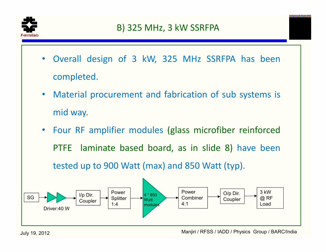
B) 325 MHz, 3 kW SSRFPA
• Overall design of 3 kW, 325 MHz SSRFPA has been
completed.
• Material procurement and fabrication of sub systems is
mid way.
• Four RF amplifier modules (glass microfiber reinforced
Manjiri / RFSS / IADD / Physics Group / BARC/India
• Four RF amplifier modules (glass microfiber reinforced
PTFE laminate based board, as in slide 8) have been
tested up to 900 Watt (max) and 850 Watt (typ).
SGPower
Splitter
1:4
4 * 850
Watt
modules
Power
Combiner
4:1Driver:40 W
3 kW
@ RF
Load
O/p Dir.
CouplerI/p Dir.
Coupler
July 19, 2012
Page 20
Power Divider Combiner(PDC)
• Its input splitter (1:4) has been fabricated and preliminary testing is being done.
• Return Loss at i/p ports: > 20 dB
• Return Loss at o/p ports: > 25 dB
• Isolation among the ports: > 25 dB
• Design of 4 way output combiner is complete and fabrication of first prototype is
almost complete
• Directional coupler and interlock circuit is under design.
Output Power combiner of 3 kW rating is similar to this
picture
input splitter (1:4)
July 19, 2012 Manjiri/RFSS/IADD/Physics Group/BARC/India
Page 21
C) 7 kW, 325 MHz SSRFPA
• Design of 7 kW, 325 MHz SSRFPA has started
• Design of combiner/splitter, directional coupler is complete and
is under fabrication. Interlock and protection circuit under
design.
• Based on experience of earlier 1 and 3 kW RF systems, a decision
on use of type of RF modules will be taken.
Manjiri / RFSS/IADD/Physics Group/BARC/India
SGPower
Splitter
1:8
8 * 900
Watt
modules
Power
Combiner
8:1
7 kW
@ RF
Load
O/p Dir.
CouplerI/p Dir.
Coupler
Driver:200W
July 19, 2012
Page 22
Summary
• Research on main building block of system i.e. RF
power module is almost over. Overall system
integration for 1 kW system has started.
• For 3 kW system, partial development of subsystems • For 3 kW system, partial development of subsystems
is in the process.
• For 7 kW RF system, design is almost complete.
July 19, 2012 Manjiri/RFSS/IADD/Physics Group/BARC/India
Page 23
RFSS Team
1. Mrs. Manjiri Pande
2. Mr. B.V.R.Rao
3. Mr. J.K.Mishra3. Mr. J.K.Mishra
4. Mrs. S.V.Sharma
5. Mrs. Sherry Rosily
6. Mr. S.Muthu
7. Mr. M. Thapad
July 19, 2012 Manjiri/RFSS/IADD/Physics Group/BARC/India
Page 24
RFSS/IADD/Physics Group/BARC/India