15
!"# $ % &’ (’ ) *

MOSFETMetal Oxide Semiconductor Field Effect Transistor
CoolMOS™ C6 650V 650V CoolMOS™ C6 Power TransistorIPS65R1K4C6
Data SheetRev. 2.0Final
Industrial & Multimarket

2
650V CoolMOS™ C6 Power Transistor
IPS65R1K4C6
Rev. 2.0, 2012-07-06Final Data Sheet
IPAK SL
drainpin 2
gatepin 1
sourcepin 3
1 DescriptionCoolMOS™ is a revolutionary technology for high voltage power MOSFETs,designed according to the superjunction (SJ) principle and pioneered byInfineon Technologies. CoolMOS™ C6 series combines the experience of theleading SJ MOSFET supplier with high class innovation. The resulting devicesprovide all benefits of a fast switching SJ MOSFET while not sacrificing ease ofuse. Extremely low switching and conduction losses make switchingapplications even more efficient, more compact, lighter and cooler.
Features• Extremely low losses due to very low FOM Rdson*Qg and Eoss• Very high commutation ruggedness• Easy to use/drive• Pb-free plating, Halogen free mold compound• Qualified for industrial grade applications according to JEDEC (J-STD20 andJESD22)
ApplicationsPFC stages, hard switching PWM stages and resonant switching PWM stagesfor e.g. PC Silverbox, Adapter, LCD & PDP TV, Lighting, Server, Telecom andUPS.
Table 1 Key Performance ParametersParameterParameterParameterParameter ValueValueValueValue UnitUnitUnitUnit
V‡» @ TÎ ÑÈà 700 V
RDS(on),max 1.4 Â
Qg,typ 10.5 nC
ID,pulse 8.3 A
Eoss @ 400V 1.15 µJ
Body diode di/dt 500 A/µs
Type / Ordering CodeType / Ordering CodeType / Ordering CodeType / Ordering Code PackagePackagePackagePackage MarkingMarkingMarkingMarking Related LinksRelated LinksRelated LinksRelated Links
IPS65R1K4C6 PG-TO 251 65C61K4 see Appendix A

3
650V CoolMOS™ C6 Power Transistor
IPS65R1K4C6
Rev. 2.0, 2012-07-06Final Data Sheet
Table of ContentsDescription . . . . . . . . . . . . . . . . . . . . . . . . . . . . . . . . . . . . . . . . . . . . . . . . . . . . . . . . . . . . . . . . . . . . . . . . . . . . . . . . . . 2
Table of Contents . . . . . . . . . . . . . . . . . . . . . . . . . . . . . . . . . . . . . . . . . . . . . . . . . . . . . . . . . . . . . . . . . . . . . . . . . . . . 3
Maximum ratings . . . . . . . . . . . . . . . . . . . . . . . . . . . . . . . . . . . . . . . . . . . . . . . . . . . . . . . . . . . . . . . . . . . . . . . . . . . . . 4
Thermal characteristics . . . . . . . . . . . . . . . . . . . . . . . . . . . . . . . . . . . . . . . . . . . . . . . . . . . . . . . . . . . . . . . . . . . . . . . 5
Electrical characteristics . . . . . . . . . . . . . . . . . . . . . . . . . . . . . . . . . . . . . . . . . . . . . . . . . . . . . . . . . . . . . . . . . . . . . . . 6
Electrical characteristics diagrams . . . . . . . . . . . . . . . . . . . . . . . . . . . . . . . . . . . . . . . . . . . . . . . . . . . . . . . . . . . . . . . 8
Test Circuits . . . . . . . . . . . . . . . . . . . . . . . . . . . . . . . . . . . . . . . . . . . . . . . . . . . . . . . . . . . . . . . . . . . . . . . . . . . . . . . 12
Package Outlines . . . . . . . . . . . . . . . . . . . . . . . . . . . . . . . . . . . . . . . . . . . . . . . . . . . . . . . . . . . . . . . . . . . . . . . . . . . 13
Appendix A . . . . . . . . . . . . . . . . . . . . . . . . . . . . . . . . . . . . . . . . . . . . . . . . . . . . . . . . . . . . . . . . . . . . . . . . . . . . . . . . 14
Revision History . . . . . . . . . . . . . . . . . . . . . . . . . . . . . . . . . . . . . . . . . . . . . . . . . . . . . . . . . . . . . . . . . . . . . . . . . . . . 15
Disclaimer . . . . . . . . . . . . . . . . . . . . . . . . . . . . . . . . . . . . . . . . . . . . . . . . . . . . . . . . . . . . . . . . . . . . . . . . . . . . . . . . . 15

4
650V CoolMOS™ C6 Power Transistor
IPS65R1K4C6
Rev. 2.0, 2012-07-06Final Data Sheet
2 Maximum ratingsat TÎ = 25°C, unless otherwise specified
Table 2 Maximum ratingsValues
Min. Typ. Max.Parameter Symbol Unit Note / Test Condition
Continuous drain current1) I ‡ 3.2 A T† = 25°C
2.0 T† = 100°C
Pulsed drain current2) I ‡‚ÔÛÐÙþ 8.3 A T† = 25°C
Avalanche energy, single pulse Eƒ» 26 mJ I ‡ = 0.6A, V‡‡ = 50V(see table 18)
Avalanche energy, repetitive Eƒ¸ 0.10 mJ I ‡ = 0.6A, V‡‡ = 50V
Avalanche current, repetitive I ƒ¸ 0.6 A
MOSFET dv/dt ruggedness dv/dt 50 V/ns V‡» = 0 ... 480V
Gate source voltage V•» -20 20 V static
-30 30 AC (f > 1 Hz)
Operating and storage temperature T΂TÙÚà -55 150 °C
Continuous diode forward current I » 2.8 A T† = 25°C
Diode pulse current I »‚ÔÛÐÙþ 8.3 A T† = 25°C
Reverse diode dv/dt3) dv/dt 15 V/ns V‡» = 0 ... 400V, I »‡ ù I ‡,TÎ = 25°C(see table 16)
Maximum diode commutation speed diË/dt 500 A/µs
Power dissipation PÚÓÚ 28 W T†=25°C
1) Limited by TÎ ÑÈà. Maximum duty cycle D=0.752) Pulse width tÔ limited by TÎ ÑÈà3) Identical low side and high side switch with identical R•

5
650V CoolMOS™ C6 Power Transistor
IPS65R1K4C6
Rev. 2.0, 2012-07-06Final Data Sheet
3 Thermal characteristicsTable 3 Thermal characteristics IPAK SL
Values
Min. Typ. Max.Parameter Symbol Unit Note / Test Condition
Thermal resistance, junction - case RÚÌœ† 4.4 °C/W
Thermal resistance, junction - ambient1) RÚÌœƒ 62 °C/W leaded
35 SMD version, device on PCB, 6cm²cooling area
Soldering temperature, wave- &reflowsoldering allowed TÙÓÐÁ 260 °C 1.6 mm (0.063 in.) from case for
10s
1) Device on 40mm*40mm*1.5mm one layer epoxy PCB FR4 with 6cm² copper area (thickness 70µm) for drain connection. PCB isvertical without air stream cooling.

6
650V CoolMOS™ C6 Power Transistor
IPS65R1K4C6
Rev. 2.0, 2012-07-06Final Data Sheet
4 Electrical characteristicsat TÎ = 25°C, unless otherwise specified
Table 4 Static characteristicsValues
Min. Typ. Max.Parameter Symbol Unit Note / Test Condition
Drain-source breakdown voltage Vñ…¸ò‡»» 650 V V•» = 0V, I ‡ = 1mA
Gate threshold voltage V•»ñÚÌò 2.5 3 3.5 V V‡» = V•», I ‡ = 0.1mA
Zero gate voltage drain current I ‡»» 1 µA V‡» = 650V, V•» = 0V, TÎ = 25°C
10 V‡» = 650V, V•» = 0V, TÎ = 150°C
Gate-source leakage current I •»» 100 nA V•» = 20V, V‡» = 0V
Drain-source on-state resistance R‡»ñÓÒò 1.260 1.4  V•» = 10V, I ‡ = 1.0A, TÎ = 25°C
3.280 V•» = 10V, I ‡ = 1A, TÎ = 150°C
Gate resistance R• 6.5 Â f = 1MHz, open drain
Table 5 Dynamic characteristicsValues
Min. Typ. Max.Parameter Symbol Unit Note / Test Condition
Input capacitance CÍÙÙ 225 pF V•» = 0V, V‡» = 100V, f = 1MHz
Output capacitance CÓÙÙ 18 pF
Effective output capacitance, energyrelated1) CÓñþØò 10 pF V•» = 0V, V‡» = 0 ... 480V
Effective output capacitance, time related2)CÓñÚØò 42 pF I ‡ = constant, V•» = 0V,
V‡» = 0 ... 480V
Turn-on delay time tÁñÓÒò 7.7 ns V‡‡ = 400V, V•» = 13V, I ‡ = 1.5A,R• = 10.2Â(see table 17)Rise time tØ 5.9 ns
Turn-off delay time tÁñÓËËò 33 ns
Fall time tË 18.2 ns
Table 6 Gate charge characteristicsValues
Min. Typ. Max.Parameter Symbol Unit Note / Test Condition
Gate to source charge QÃÙ 1.3 nC V‡‡ = 480V, I ‡ = 1.5A,V•» = 0 to 10V
Gate to drain charge QÃÁ 5.8 nC
Gate charge total QÃ 10.5 nC
Gate plateau voltage VÔÐÈÚþÈÛ 5.4 V
1) CÓñþØò is a fixed capacitance that gives the same stored energy as CÓÙÙ while V‡» is rising from 0 to 80% Vñ…¸ò‡»»2) CÓñÚØò is a fixed capacitance that gives the same charging time as CÓÙÙ while V‡» is rising from 0 to 80% Vñ…¸ò‡»»

7
650V CoolMOS™ C6 Power Transistor
IPS65R1K4C6
Rev. 2.0, 2012-07-06Final Data Sheet
Table 7 Reverse diode characteristicsValues
Min. Typ. Max.Parameter Symbol Unit Note / Test Condition
Diode forward voltage V»‡ 0.9 V V•» = 0V, I Œ = 1.5A, TÎ = 25°C
Reverse recovery time tØØ 200 ns V¸ = 400V, I Œ = 1.5A,di Œ/dt = 100A/µs(see table 16)Reverse recovery charge QØØ 0.9 µC
Peak reverse recovery current I ØØÑ 8 A

8
650V CoolMOS™ C6 Power Transistor
IPS65R1K4C6
Rev. 2.0, 2012-07-06Final Data Sheet
5 Electrical characteristics diagrams
Table 8Power dissipationPower dissipationPower dissipationPower dissipation
TTTTCCCC [°C] [°C] [°C] [°C]
PP PPto
tto
tto
tto
t [W
] [
W]
[W
] [
W]
0 40 80 120 1600
5
10
15
20
25
30
Ptot=f(TC)
Max. transient thermal impedanceMax. transient thermal impedanceMax. transient thermal impedanceMax. transient thermal impedance
ttttpppp [s] [s] [s] [s]
ZZ ZZth
JC
thJ
Cth
JC
thJ
C [
K/W
] [
K/W
] [
K/W
] [
K/W
]
10-5 10-4 10-3 10-2 10-110-2
10-1
100
101
0.5
0.2
0.1
0.05
0.02
0.01single pulse
ZthJC =f(tP); parameter: D=tp/T
Table 9Safe operating areaSafe operating areaSafe operating areaSafe operating area
VVVVDSDSDSDS [V] [V] [V] [V]
I I I I DD DD
[A
] [
A]
[A
] [
A]
100 101 102 10310-2
10-1
100
101
102
1 µs
10 µs
100 µs
1 ms
10 ms
DC
I D=f(VDS); VGS>7V;TC=25°C; D=0; parameter: tp
Safe operating areaSafe operating areaSafe operating areaSafe operating area
VVVVDSDSDSDS [V] [V] [V] [V]
I I I I DD DD
[A
] [
A]
[A
] [
A]
100 101 102 10310-2
10-1
100
101
102
1 µs
10 µs
100 µs
1 ms
10 ms
DC
I D=f(VDS); VGS>7V;TC=80°C; D=0; parameter: tp
9
650V CoolMOS™ C6 Power Transistor
IPS65R1K4C6
Rev. 2.0, 2012-07-06Final Data Sheet
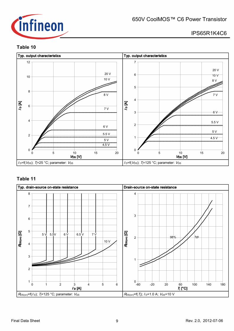
Table 10Typ. output characteristicsTyp. output characteristicsTyp. output characteristicsTyp. output characteristics
VVVVDSDSDSDS [V] [V] [V] [V]
I I I I DD DD
[A
] [
A]
[A
] [
A]
0 5 10 15 200
2
4
6
8
10
12
20 V
10 V
8 V
7 V
6 V
5.5 V
5 V
4.5 V
I D=f(VDS); Tj=25 °C; parameter: VGS
Typ. output characteristicsTyp. output characteristicsTyp. output characteristicsTyp. output characteristics
VVVVDSDSDSDS [V] [V] [V] [V]
I I I I DD DD
[A
] [
A]
[A
] [
A]
0 5 10 15 200
1
2
3
4
5
6
7
20 V
10 V
8 V
7 V
6 V
5.5 V
5 V
4.5 V
I D=f(VDS); Tj=125 °C; parameter: VGS
Table 11Typ. drain-source on-state resistanceTyp. drain-source on-state resistanceTyp. drain-source on-state resistanceTyp. drain-source on-state resistance
I I I I DDDD [A] [A] [A] [A]
RR RRD
S(o
n)
DS
(on
)D
S(o
n)
DS
(on
) [Â
] [
Â]
[Â
] [
Â]
0 1 2 3 4 5 61
2
3
4
5
6
7
8
6 V5.5V5 V 6.5 V 7 V
10 V
RDS(on)=f(I D); Tj=125 °C; parameter: VGS
Drain-source on-state resistanceDrain-source on-state resistanceDrain-source on-state resistanceDrain-source on-state resistance
TTTTjjjj [°C] [°C] [°C] [°C]
RR RRD
S(o
n)
DS
(on
)D
S(o
n)
DS
(on
)[Â
][Â
][Â
][Â
]
-60 -20 20 60 100 140 1800
1
2
3
4
98% typ
RDS(on)=f(Tj); I D=1.0 A; VGS=10 V

10
650V CoolMOS™ C6 Power Transistor
IPS65R1K4C6
Rev. 2.0, 2012-07-06Final Data Sheet
Table 12Typ. transfer characteristicsTyp. transfer characteristicsTyp. transfer characteristicsTyp. transfer characteristics
VVVVGSGSGSGS [V] [V] [V] [V]
I I I I DD DD
[A
] [
A]
[A
] [
A]
0 2 4 6 8 100
2
4
6
8
10
150 °C
25 °C
I D=f(VGS); VDS = 20V; parameter: Tj
Typ. gate chargeTyp. gate chargeTyp. gate chargeTyp. gate charge
QQQQgategategategate [nC] [nC] [nC] [nC]
VV VVG
SG
SG
SG
S [
V]
[V
] [
V]
[V
]
0 5 10 150
1
2
3
4
5
6
7
8
9
10
480 V120 V
VGS=f(Qgate); I D=1.5 A pulsed; parameter: VDD
Table 13Avalanche energyAvalanche energyAvalanche energyAvalanche energy
TTTTjjjj [°C] [°C] [°C] [°C]
EE EEA
SA
SA
SA
S [
mJ]
[m
J] [
mJ]
[m
J]
0 50 100 150 2000
5
10
15
20
25
30
EAS=f(Tj); I D=0.6 A; VDD=50 V
Drain-source breakdown voltageDrain-source breakdown voltageDrain-source breakdown voltageDrain-source breakdown voltage
TTTTjjjj [°C] [°C] [°C] [°C]
VV VVB
R(D
SS
)B
R(D
SS
)B
R(D
SS
)B
R(D
SS
) [V
] [
V]
[V
] [
V]
-60 -20 20 60 100 140 180550
575
600
625
650
675
700
725
750
VBR(DSS)=f(Tj); I D=1.0 mA
11
650V CoolMOS™ C6 Power Transistor
IPS65R1K4C6
Rev. 2.0, 2012-07-06Final Data Sheet
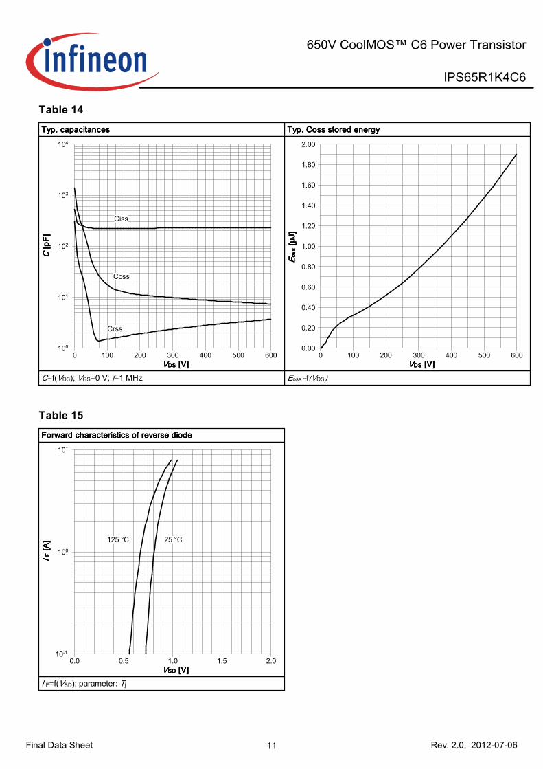
Table 14Typ. capacitancesTyp. capacitancesTyp. capacitancesTyp. capacitances
VVVVDSDSDSDS [V] [V] [V] [V]
CC CC [
pF
] [
pF
] [
pF
] [
pF
]
0 100 200 300 400 500 600100
101
102
103
104
Ciss
Coss
Crss
C=f(VDS); VGS=0 V; f=1 MHz
Typ. Coss stored energyTyp. Coss stored energyTyp. Coss stored energyTyp. Coss stored energy
VVVVDSDSDSDS [V] [V] [V] [V]
EE EEo
ss
os
so
ss
os
s [
µJ]
[µ
J] [
µJ]
[µ
J]
0 100 200 300 400 500 6000.00
0.20
0.40
0.60
0.80
1.00
1.20
1.40
1.60
1.80
2.00
Eoss=f(VDS)
Table 15Forward characteristics of reverse diodeForward characteristics of reverse diodeForward characteristics of reverse diodeForward characteristics of reverse diode
VVVVSDSDSDSD [V] [V] [V] [V]
I I I I FF FF
[A
] [
A]
[A
] [
A]
0.0 0.5 1.0 1.5 2.010-1
100
101
125 °C 25 °C
I F=f(VSD); parameter: Tj

12
650V CoolMOS™ C6 Power Transistor
IPS65R1K4C6
Rev. 2.0, 2012-07-06Final Data Sheet
6 Test Circuits
Table 16 Diode characteristicsTest circuit for diode characteristics Diode recovery waveform
VDS
IDRG1
RG2
RG1 = RG2
Table 17 Switching times
VDSVGS
VDS
VGS
td(on) td(off)tr
ton
tf
toff
10%
90%
Switching times test circuit for inductive load Switching times waveform
Table 18 Unclamped inductiveUnclamped inductive load test circuit Unclamped inductive waveform
VDSID
VDS
VD
V(BR)DS
IDVDS

13
650V CoolMOS™ C6 Power Transistor
IPS65R1K4C6
Rev. 2.0, 2012-07-06Final Data Sheet
7 Package Outlines
Figure 1 Outline PG-TO 251, dimensions in mm/inches

14
650V CoolMOS™ C6 Power Transistor
IPS65R1K4C6
Rev. 2.0, 2012-07-06Final Data Sheet
8 Appendix A
Table 19 Related Links
• IFX C6 Product Brief:
http://www.infineon.com/dgdl/Product+Brief+600V+CoolMOS+C6+.pdf?folderId=db3a3043156fd5730115939eb6b506db&fileId=db3a304320d39d590121ca3c002f00db
• IFX C6 Portfolio:http://www.infineon.com/cms/en/product/findProductTypeByName.html?q=ip*c6
• IFX CoolMOS Webpage:http://www.infineon.com/cms/en/product/channel.html?channel=ff80808112ab681d0112ab6a628704d8
• IFX Design Tools:http://www.infineon.com/cms/en/product/promopages/designtools/index.html

15
650V CoolMOS™ C6 Power Transistor
IPS65R1K4C6
Rev. 2.0, 2012-07-06Final Data Sheet
Revision HistoryIPS65R1K4C6
Revision: 2012-07-06, Rev. 2.0Revision: 2012-07-06, Rev. 2.0Revision: 2012-07-06, Rev. 2.0Revision: 2012-07-06, Rev. 2.0
Previous Revision
Revision Date Subjects (major changes since last revision)
0.9 2011-12-19 Release of target datasheet
2.0 2012-07-06 Release of final version
We Listen to Your CommentsAny information within this document that you feel is wrong, unclear or missing at all? Your feedback will help us to continuouslyimprove the quality of this document. Please send your proposal (including a reference to this document) to:[email protected]
Edition 2011-08-01Published byInfineon Technologies AG81726 München, Germany© 2011 Infineon Technologies AGAll Rights Reserved.
Legal DisclaimerThe information given in this document shall in no event be regarded as a guarantee of conditions or characteristics. With respectto any examples or hints given herein, any typical values stated herein and/or any information regarding the application of thedevice, Infineon Technologies hereby disclaims any and all warranties and liabilities of any kind, including without limitation,warranties of non-infringement of intellectual property rights of any third party.
InformationFor further information on technology, delivery terms and conditions and prices please contact your nearest Infineon TechnologiesOffice (www.infineon.com).
WarningsDue to technical requirements, components may contain dangerous substances. For information on the types in question, pleasecontact the nearest Infineon Technologies Office.The Infineon Technologies component described in this Data Sheet may be used in life-support devices or systems and/orautomotive, aviation and aerospace applications or systems only with the express written approval of Infineon Technologies, if afailure of such components can reasonably be expected to cause the failure of that life-support, automotive, aviation and aerospacedevice or system or to affect the safety or effectiveness of that device or system. Life support devices or systems are intended to beimplanted in the human body or to support and/or maintain and sustain and/or protect human life. If they fail, it is reasonable toassume that the health of the user or other persons may be endangered.


