Infrared optical constants and roughness factor functions determination: the HTHRTR method Marta Klanjsek Gunde and Boris Aleksandrov This method was developed to determine the complex infrared optical constant of a single free-standing partially absorbing plate as wellas a thin solid film deposited on it. The method is based on exact formulasfor normal transmittance T and near-normal reflectance R of the substrate as well as the film-substrate double layer. Coherent multiple reflections throughout the film and incoherent multiple reflections in the substrate as well as the intensity losses on the rough surface are taken into account. The influence of various data on the solution of the inverseproblem is discussed by a contour map study. The method is explained using examples of both- and single-side-polished silicon wafers where the transmission and reflection roughness factor functions HTHR are determined for the rough surface. The thin-film example has been the silicon oxide film formed on the single-side-polished silicon substrate by chemical vapor deposition. 1. Introduction Optical properties of any material are fully determined by spectral dependence of the complex optical con- stant h(X), which consists of the refractive index n(X) and the extinction coefficient k(X), and [n(X), k(X)] are known as optical constants. Spectral phenomena studies, for example, some of the various sum rules, physical models for dielectric function, or some appli- cations as photothermal solar energy conversion radia- tive cooling, etc. require knowledge of optical con- stants over a wide wavelength range. Here the infrared (IR) spectral region is of crucial importance. We started optical constant studies to eliminate some of the unfavorable features of the measured IR spectra of thin solid films deposited on various kinds of substrate. Optical constants of some materials may be taken from the literature,' but for a more precise study it is better to obtain them by measurement of the sample. In some cases the extinction coefficient k(X) in the mid-IR region may be obtained from absorbance spectra. In general, accompanying problems, such as baseline corrections, backside roughness, thick sam- M. K. Gunde is with the Boris Kidri6 Institute of Chemistry, Hajdrihova 19, Ljubljana, P.O. Box 30, YU-61115 Ljubljana, Yugo- slavia. When the research was performed B. Aleksandrov was with the Iskra Microelectronics, Ljubljana, Yugoslavia. He is currently with Avtotehna Ljubljana, Titova 36, Yugoslavia. Received 20 February 1991. 0003-6935/91/223186-11$05.00/0. C 1991 Optical Society of America. ples, high absorbance, etc., must be considered. If the thin film is under measurement, the multiple reflec- tance effect causes the superposition of the interfer- ence fringes on the measured spectra. The quantita- tive estimation of spectral properties becomes difficult or sometimes quite impossible to work out. Contrary to the measured absorbance spectra, optical constants n(X)and k(X)depend only on the material and are free of any other effects. The literature reports several methods for determin- ing optical constants of different materials. Two basic classes of techniques can be distinguished: ellipsome- tric and photometric. In ellipsometric methods the amplitude and phase of the reflected wave are com- pared with those of the incident wave. The measure- ments are usually restricted to the ellipsometer's oper- ating wavelength. The photometric techniques are based on measurements of reflected and/or transmit- ted intensity at given polarization and incident angle. To determine optical constants over a wide spectral region, photometric methods are commonly used. If only one optical measurement is performed, it is combined by the causality relation between the optical constants. Use of the Kramers-Kronig (K-K) disper- sion relation to convert the bulk reflectance data to optical constants is well known from the sixties. 2 K- K analysis of the absorption spectrum was also report- ed. 5 The numerical programs that perform the calcu- lation of optical constants by means of the K-K disper- sion relation are now commercially available from spectrophotometer manufacturers. The required ex- perimental data over an extremely wide frequency range could be the drawback of the method. For 3186 APPLIED OPTICS / Vol. 30, No. 22 / 1 August 1991
Transcript
Infrared optical constants and roughness factor functionsdetermination: the HTHRTR method
Marta Klanjsek Gunde and Boris Aleksandrov
This method was developed to determine the complex infrared optical constant of a single free-standingpartially absorbing plate as wellas a thin solid film deposited on it. The method is based on exact formulas fornormal transmittance T and near-normal reflectance R of the substrate as well as the film-substrate doublelayer. Coherent multiple reflections throughout the film and incoherent multiple reflections in the substrateas well as the intensity losses on the rough surface are taken into account. The influence of various data on thesolution of the inverse problem is discussed by a contour map study. The method is explained using examplesof both- and single-side-polished silicon wafers where the transmission and reflection roughness factorfunctions HTHR are determined for the rough surface. The thin-film example has been the silicon oxide filmformed on the single-side-polished silicon substrate by chemical vapor deposition.
1. Introduction
Optical properties of any material are fully determinedby spectral dependence of the complex optical con-stant h(X), which consists of the refractive index n(X)and the extinction coefficient k(X), and [n(X), k(X)] areknown as optical constants. Spectral phenomenastudies, for example, some of the various sum rules,physical models for dielectric function, or some appli-cations as photothermal solar energy conversion radia-tive cooling, etc. require knowledge of optical con-stants over a wide wavelength range. Here theinfrared (IR) spectral region is of crucial importance.
We started optical constant studies to eliminatesome of the unfavorable features of the measured IRspectra of thin solid films deposited on various kinds ofsubstrate. Optical constants of some materials maybe taken from the literature,' but for a more precisestudy it is better to obtain them by measurement of thesample. In some cases the extinction coefficient k(X)in the mid-IR region may be obtained from absorbancespectra. In general, accompanying problems, such asbaseline corrections, backside roughness, thick sam-
M. K. Gunde is with the Boris Kidri6 Institute of Chemistry,Hajdrihova 19, Ljubljana, P.O. Box 30, YU-61115 Ljubljana, Yugo-slavia. When the research was performed B. Aleksandrov was withthe Iskra Microelectronics, Ljubljana, Yugoslavia. He is currentlywith Avtotehna Ljubljana, Titova 36, Yugoslavia.
Received 20 February 1991.0003-6935/91/223186-11$05.00/0.C 1991 Optical Society of America.
ples, high absorbance, etc., must be considered. If thethin film is under measurement, the multiple reflec-tance effect causes the superposition of the interfer-ence fringes on the measured spectra. The quantita-tive estimation of spectral properties becomes difficultor sometimes quite impossible to work out. Contraryto the measured absorbance spectra, optical constantsn(X) and k(X) depend only on the material and are freeof any other effects.
The literature reports several methods for determin-ing optical constants of different materials. Two basicclasses of techniques can be distinguished: ellipsome-tric and photometric. In ellipsometric methods theamplitude and phase of the reflected wave are com-pared with those of the incident wave. The measure-ments are usually restricted to the ellipsometer's oper-ating wavelength. The photometric techniques arebased on measurements of reflected and/or transmit-ted intensity at given polarization and incident angle.To determine optical constants over a wide spectralregion, photometric methods are commonly used.
If only one optical measurement is performed, it iscombined by the causality relation between the opticalconstants. Use of the Kramers-Kronig (K-K) disper-sion relation to convert the bulk reflectance data tooptical constants is well known from the sixties.2 K-K analysis of the absorption spectrum was also report-ed.5 The numerical programs that perform the calcu-lation of optical constants by means of the K-K disper-sion relation are now commercially available fromspectrophotometer manufacturers. The required ex-perimental data over an extremely wide frequencyrange could be the drawback of the method. For
weakly absorbing films on transparent substrates theenvelope method was reported where, instead of thesecond optical measurement, the appropriate ap-proach is applied.6 -9 Only the transmission spectrumis usually required. The thickness of the film is calcu-lated on the basis of interference fringes whereas forthe optical constants both envelopes of the spectrumare used.
The commonly used technique to determine opticalconstants of absorbing materials involves at least twooptical measurements, usually transmission and re-flection, i.e., the T, R method.'0-' 6 The thickness ofthe sample is supposed to be known. The optical pathof the beam in the experiment is described by means ofgeneralized Fresnel equations, which, together withmeasured spectra, offer unknown optical constants.The advantage of the method is its generality. Be-sides the necessity for well-defined optical constants,i.e., a homogeneous and isotropic material, no otherassumption is needed. Therefore, a large spectralvariation of optical data can also be studied. Suchvariation is expected in the IR region, and to considerthis spectral region using optical constants we chosethis determination method.
The solutions of the equation system can be deter-mined by the intersections of Rexp = R(n, k) and Texp =T(n, k) contours in the (n, k) plane. Another possibili-ty is to obtain a set of all the possible solutions usingone of the numerical methods. The former is the so-called graphic method that is suitable to analyze thedifficulties of the inverse photometric problem, i.e.,multiple solutions and missing solutions. The opticalpath of the beam is mathematically described by apolynomial where the optical constants represent vari-ables. This is the origin of the existence of multiplesolutions. All the solutions are in fact pairs of num-bers, as can be clearly seen from the contour map.Only one pair of optical constants is physically reason-able. If the contour lines do not intersect, the particu-lar solution is missed. Provided that the optical pathof the beam in the experiment is well described byoptical constants (without large simplification), thiswould be the only reason for experimental error. It isconvenient to discuss this error with the help of aparticular contour map. The intersections in the (n,k) plane are in practice also calculated by a computer,applying a suitable numerical method.
The literature reports on some contour maps, butonly in a few publications are they studied more or lessin detail.'0"13 The commonly used substrate is strictlytransparent; sometimes only the metallic one is report-ed.13"15 It has been reported that the metallized sub-strate in some regions of the (n, k) plane increases thesmall intersection angle of the contours. The effect ofthe substrate extinction coefficient on the contourmap is, therefore, shown in only two limiting cases.
In general, studying light scattering on rough sur-faces is a difficult task. In optical constant studiessurface roughness represents a source of systemic er-rors. Some work has been reported where the rough-ness was considered.1 7 -'9 Surface imperfection was
introduced in the Fresnel amplitude factor in expo-nential form. The Gaussian distribution of surfaceheights was assumed and only reflection was usuallycorrected.
Scattering caused by roughness is important for sili-con wafers, which normally have only one side polishedfront side), whereas the other remains rough. Thespectral dependence of wafer transmittance and re-flectance is strongly influenced by the scattering be-havior of the rough backside.20 Radiative scatteringwas reported to be the main source of errors in determi-nation of oxygen in silicon by the IR method. 2 '
Our study of thin solid film coating on partiallyabsorbing substrates consists of two parts: first, thedetermination of substrate optical constants and sec-ond, the determination of thin-film optical constants.To keep it simple and to avoid the possibility of errorscaused by internal polarization effects in the opticalsystem and angular measurements, the nonpolarizednormal transmittance (7) and near-normal reflectance(R) are to be measured. If the rear side is rough, theroughness factor functions for reflected HR and trans-mitted HT intensities were obtained and the opticalconstants were calculated. Out of several studied sub-strates and thin solid films, only one example is shown:silicon oxide film deposited on a silicon wafer. Thesingle-side-polished silicon wafer is compared to aboth-side-polished sample. For the rough rear sidethe roughness factor functions are determined. Theinherent difficulties of the inverse problem are dis-cussed extensively for the thin solid supported films.
II. Equations
First, we derive the equations for the particular caseswhere all the surfaces are specular. Then, the equa-tions for the rough surfaces are given.
A. Substrate
We consider a plane parallel plate of a homogeneousand isotropic material. We also assume that bothsurfaces of the plate are specular. The required ex-perimental conditions are shown in Fig. la, where forbetter understanding the oblique instead of normalincidence is shown. The plate is free standing. Thesurrounding medium has frequency independent opti-cal constants (ho = 3 = 1). The electromagnetic beamis partially reflected and transmitted at each boundaryaccording to the Fresnel equations. The thickness ofthe slab is much greater than the wavelength of inter-est. The resulting total reflectance R and total trans-mittance T are the sum of the successively transmittedand reflected beam intensities:
Fig. 1. Intensities of the beams reflected and transmitted successively at the front and rear surfaces (a) of the substrate and (b) of the film-substrate double layer at oblique incidence. All the surfaces are specular.
Rij = ijPi, (4)
are the transmitted and reflected intensities at theboundary between the ith and jth medium,
F = exp(-42rk 2 D/X)
The double-index intensities are the subjects of Eqs.(3) and (4) and F is the internal transmission of thesubstrate [Eq. (5)]. In the triple-index intensities thecoherent summation is taken into account:
Tiji= - , l ijlrijl*
(6) Rij = hijlbijl*.
(5)
is the internal transmission of a slab with thickness D,
hi(X) = ni(X) - iki(X)
is the wavelength-dependent complex optical constantof medium i, and tEi and iij are the Fresnel amplitudereflection and transmission coefficients on the bound-ary between medium i and medium j.22 Using a com-bination of Eqs. (l)-(6) we get the following implicitsystem:
T = T[n2 (X), k2(X), D],
R = R[n2 (X), k 2(X), D]. (7)
B. Thin Solid Supported Film
We treated substrate-type film as shown in Fig. lb.The thickness of a substrate (D) is much greater thanthe wavelength used, whereas the thickness of the film(d) is of the order of the wavelength. The coherentmultiple reflection of the beam in the thin film andincoherent summation of the successively transmittedand reflected beam intensities throughout the sub-strate are taken into account. The resulting totaltransmittance T and total reflectance R are the sum ofthe successively transmitted and reflected intensities:
T T012FT23 ,(8)
1 - P2R23R210 (
R -R012+ T 012FR 23 T210 (9)1 - F2R 23R 21 0
(10)
(11)
The transmission and reflection amplitude coeffi-cients in the direction i I are obtained byapplying the well-known summation method22:
t^,tjl exp(-ib)~I. =1 + PijPjl exp(-2i)'
= PijPjl exp(-2i)I1 + PijPjl exp(-2iW)
(12)
(13)
Here Pij and Eij are the Fresnel amplitude reflection andtransmission coefficients for the boundary betweenmedium i and medium j in the direction i j. represents the phase change of the beam traversing thefilm of thickness d:
&= 2wAld;-A h d (14)
hA is the complex optical constant of the film. Byappropriate combination of Eqs. (8)-(14) and (3)-(6)we obtain the following implicit equation system:
T = T[ni(X), k(X), d, n 2(X), k 2(X), DI,
R = R[nl(\), kl(X), d, n2(X), k 2(X), D]. (15)
C. Rough Surface
Surface roughness reduces the amount of light that onthe sample boundaries follows Snell's law. The conse-
quences are reflection and transmission losses on thenonspecular boundary between two materials. Thenormal-incidence reflection from a rough surface (Rr)can be written in the following form2 3:
Rr(X) = RS(X)HR(X,.* ), (16)
where R, is the normal-incidence reflection of a specu-lar surface of the same material and HR is a reflectionroughness factor function that reduces Rr from the R,value. For the beam intensity transmitted throughthe same rough surface we assume the relation24
T,(X) = TS(X)HT(X,--.) (17)
where T is the normal-incidence reflection of a specu-lar surface of the same material and HTis the transmis-sion roughness factor function. The HR function isonly surface dependent,2 3 whereas the HT functionshould have additional dependence on JIr of the mate-rial. In Eqs. (16) and (17) we omitted the indicesmarking the direction of the beam with regard to thesequence of the media.
Considering the rough surface by means of Eqs. (16)and (17), it is possible to treat practically any surface ofthe sample as rough. As an example here we write onlythe equations for the free-standing one-side-polishedplate. The rear surface (surface 23) of the sample issubject to Eqs. (16) and (17). Total transmittance Tand total reflectance R for selected X are, therefore, asfollows:
(18)T= TO2 FHTT231 - F2R23 HRR2O'
R = R02 + To 2 F2R23HRT2O1- F2R23HRR20
Finally, we get a modification of the implicit system inEqs. (7):
T = T[n2 (Q), k2(X), D, HR(X), HT(A)],
R = R[n2 (A), k2 (W, D, HR(X)1. (20)
Ill. Characteristic Surfaces and Contour Maps
The inherent difficulties of the inverse problem havetheir origin in the T(n,k) and R(n,k) functions. Char-acteristic surfaces as well as the contour maps are thedirect way to visualize these functions. Such a study isimportant to analyze the of the inverse problem diffi-culties as well as the ability of the method to offer goodresults. Here the characteristic surfaces and contourmaps are given for thin solid supported films as well asfor the substrate alone.
A. Substrate
At fixed X and D Eqs. (7) represent two characteristicsurfaces, T(n2, k2) and R(n2, k2). The correspondingmeasured values Texp and Rexp on these surfaces de-scribe two isocurves. The projections of both curveson the same (n2 , k 2 ) plane generally have more inter-sections, which represent the solutions of the inverseproblem. For D = 0.5 mm and X = 0.01 mm both
(19) Fig. 2. The T(n 2 , k 2) and R(n 2 , k 2) planes (arbitrary units) for a 0.5-mm thick plate at A = 0.01 mm (1000 cm-').
characteristic surfaces are illustrated in Fig. 2. Theprojections on the (n2, k 2) plane with intersections forRexp = 0.45 and Texp = 0.53 are represented in Fig. 3.The spreading of contour lines caused by experimentalerror is also shown. The two intersections in the(n2,k2) plane are separated enough on the n2-axis,therefore, it is simple to choose the right one. Theintersections lead to good accuracy in k2, whereas in n2sometimes it is worse. To improve the refractive-index accuracy, it is possible to derive the n(X) fromk(X) by the K-K integral.
B. Thin Solid supported Film
Reflection and transmission surfaces above the (n1, k1)plane and contour maps of corresponding isocurveschange at each spectral position where (d/X) is not theonly parameter defining this change. In our study thesubstrate optical constants are spectral dependent,which is the main difference in other studies reportedin this field. For this reason the shapes of characteris-tic surfaces and the corresponding contour maps alsodepend on the spectral variation of the substrate char-acteristics.
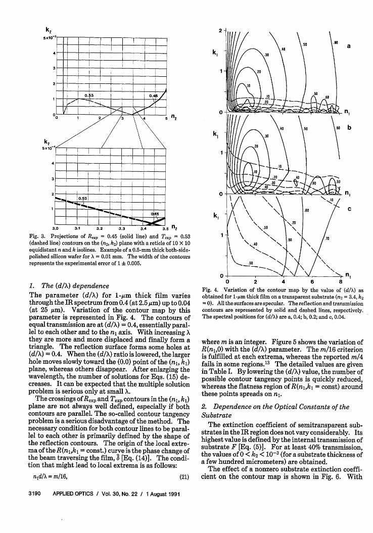
Fig. 3. Projections of Rexp = 0.45 (solid line) and Tp = 0.53(dashed line) contours on the (n2 , k2 ) plane with a reticle of 10 X 10equidistant n and k isolines. Example of a 0.5-mm thick both-side-polished silicon wafer for = 0.01 mm. The width of the contoursrepresents the experimental error of 1 I 0.005.
1. The (d/X) dependenceThe parameter (d/X) for -Am thick film variesthrough the IR spectrum from 0.4 (at 2.5 m) up to 0.04(at 25 gim). Variation of the contour map by thisparameter is represented in Fig. 4. The contours ofequal transmission are at (d/X) = 0.4, essentially paral-lel to each other and to the n axis. With increasing they are more and more displaced and finally form atriangle. The reflection surface forms some holes at(dA) = 0.4. When the (dA) ratio is lowered, the largerhole moves slowly toward the (0.0) point of the (nl, k1)plane, whereas others disappear. After enlarging thewavelength, the number of solutions for Eqs. (15) de-creases. It can be expected that the multiple solutionproblem is serious only at small X.
The crossings of Rexp and Texp contours in the (n1, k1)plane are not always well defined, especially if bothcontours are parallel. The so-called contour tangencyproblem is a serious disadvantage of the method. Thenecessary condition for both contour lines to be paral-lel to each other is primarily defined by the shape ofthe reflection contours. The origin of the local extre-ma of the R(nl,k = const.) curve is the phase change ofthe beam traversing the film, [Eq. (14)]. The condi-tion that might lead to local extrema is as follows:
nid/X= m/16, (21)
1
0
a
b
C
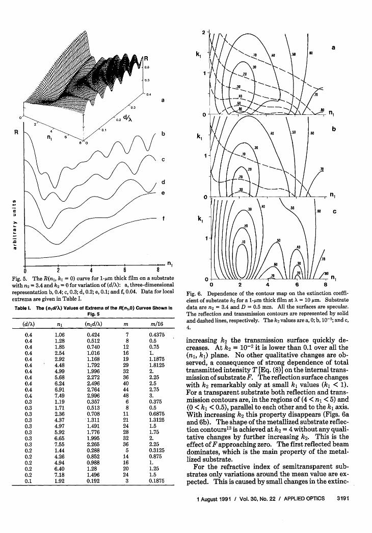
0 2 4 6 8Fig. 4. Variation of the contour map by the value of (d/X) asobtained for 1-im thick film on a transparent substrate (n2 = 3.4, k 2
= 0). All the surfaces are specular. The reflection and transmissioncontours are represented by solid and dashed lines, respectively.The spectral positions for (d/X) are a, 0.4; b, 0.2; and c, 0.04.
where m is an integer. Figure 5 shows the variation ofR(ni,0) with the (d/A) parameter. The m/16 criterionis fulfilled at each extrema, whereas the reported m/4fails in some regions.13 The detailed values are givenin Table I. By lowering the (d/X) value, the number ofpossible contour tangency points is quickly reduced,whereas the flatness region of R(nl,k1 = const) aroundthese points spreads on n1.
2. Dependence on the Optical Constants of theSubstrate
The extinction coefficient of semitransparent sub-strates in the IR region does not vary considerably. Itshighest value is defined by the internal transmission ofsubstrate F [Eq. (5)]. For at least 40% transmission,the values of 0 < k2 < 10-3 (for a substrate thickness ofa few hundred micrometers) are obtained.
The effect of a nonzero substrate extinction coeffi-cient on the contour map is shown in Fig. 6. With
Fig. 5. The R(ni, kl = 0) curve for 1-Aum thick film on a substratewith n2 = 3.4 and k2 = 0 for variation of (d/): a, three-dimensionalrepresentation b, 0.4; c, 0.3; d, 0.2; e, 0.1; and f, 0.04. Data for localextrema are given in Table I.
Table 1. The (nidlX) Values of Extrerna of the R(n,,O) Curves Shown InFig. 5
Fig. 6. Dependence of the contour map on the extinction coeffi-cient of substrate k 2 for a 1-gm thick film at X = 10 Am. Substratedata are n2 = 3.4 and D = 0.5 mm. All the surfaces are specular.The reflection and transmission contours are represented by solidand dashed lines, respectively. The k 2 values are a, 0; b, 10-3; and c,4.
increasing k2 the transmission surface quickly de-creases. At k2 = 10-2 it is lower than 0.1 over all the(n1, k1) plane. No other qualitative changes are ob-served, a consequence of strong dependence of totaltransmitted intensity T [Eq. (8)] on the internal trans-mission of substrate F. The reflection surface changeswith k 2 remarkably only at small k1 values (k1 < 1).For a transparent substrate both reflection and trans-mission contours are, in the regions of (4 < n1 < 5) and(0 < k < 0.5), parallel to each other and to the k1 axis.With increasing k2 this property disappears (Figs. 6aand 6b). The shape of the metallized substrate reflec-tion contours1 3 is achieved at k2 = 4 without any quali-tative changes by further increasing k2. This is theeffect of F approaching zero. The first reflected beamdominates, which is the main property of the metal-lized substrate.
For the refractive index of semitransparent sub-strates only variations around the mean value are ex-pected. This is caused by small changes in the extinc-
Table 11. Computation Precision According to Input Parameters and theNumber of Recursion Stepsa
Initial Following MagnifyingReticle Reticle Steps n2 k2 (X10-6)
100 X 100 10 X 10 0 3.410946 3.7942100 X 100 10 X 10 1 3.411403 3.5632100 X 100 10 X 10 2 3.411406 3.561850 X 50 10 X 10 0 3.410440 4.066350 X 50 10 X 10 1 3.411350 3.589750 X 50 10 X 10 2 3.411406 3.5620
a n2 and k2 were calculated for silicon at various computation stepsand experimental values of Rexp = 0.4568 and Txp = 0.5338 oncomputation intervals n2 = [3.. .3.8] and k 2 = [ .. .0.003].
tion coefficient. It was discovered that such smallvariations of n2 practically do not influence the map ofconstant transmission and reflection of the thin solidfilm.
IV. Calculations
We have written a computer program that can locateall intersections of Rexp = R(n, k) and Texp = T(n, k)contours on the selected interval of n and k in the (n, k)plane. Here the indices marking the media are omit-ted. The procedure can be simply described by graph-ic presentation. On the selected (n, k) plane we draw areticle of a user-selectable number of equidistant n andk isolines (Fig. 3). For each crossing point we calculateR(n, k) and T(n, k). The unit cell on the (n, k) plane isdetermined by four crossing points. For each unit cellwe can rapidly check if it has parts of both contourlines and if they intersect. If so, we use linear interpo-lation to compute the intersection coordinates n and k.For better precision we repeat the above procedure ofmapping and searching on this unit cell (Fig. 3). Witha high-resolution initial reticle (100 X 100), we have thegreat probability of not losing any solution. By addi-tional focusing on a selected cell with a (10 X 10)reticle, with a few steps we obtain the desired computa-tion precision. According to the available computerand investigated material we can choose the optimumbetween computation precision and speed. Mostly weneed just two runs for the 0.01% calculation precision(see Table II). All the solutions are temporarily storedon disk file. With another program in user-definedconditions, given intervals for n and k, continuity, etc.,from multiple solutions written on this disk file it ispossible to select the correct solution.
V. Example
To illustrate the method we discuss the results ob-tained for silicon oxide film. For the substrate, weused an n-type 0.55-mm thick single-side-polishedCzochralski-grown (CZ) silicon wafer. The oxygencontent as determined by the known IR method20 was6.9 X 1017 cm-3. SiO, film was deposited by chemicalvapor deposition at 3500C. The deposition rate was66.3 nm/min. The annealing was done at 9000C in thenitrogen atmosphere for 15 min. The average thick-ness of the oxide, as measured by ellipsometry, was
0.6-
05i RxP
0.4
0.344000 3000 2000 1000
wave number (cm-')Fig. 7. IR spectra of both-side-polished 0.491-mm thick FZ siliconwafer: normal-incidence transmittance (solid line) and near-nor-mal-incidence reflectance (dashed line).
3.422
3.421
3.
4000 3000 2000 1000
wave number (cm-')
Fig. 8. Calculated optical constants for FZ silicon wafer: extinc-tion coefficient k2 (solid line) and refractive index n2 (dashed line).
1086 25 nm. First, the optical constants of thesubstrate as well as the corresponding roughness factorfunctions were determined, and then the thin-filmoptical constants were calculated.
Spectrophotometric measurements in the 4000-400-cm'1 region with 8-cm'1 resolution were accom-plished with a Fourier transform IR spectrophotome-ter (Digilab FTS-80). The accuracy of the Fouriertransform IR spectrophotometric measurementsshould be as good as possible, at least 1 + 0.005. Thereflectance spectra were examined by a specular near-normal reflectance cell with an incident angle of -8.All reflectance spectra were measured with respect tothe reference mirror.
A. Silicon Substrate
First, optical constants of a both-side-polished floatzone (FZ) silicon wafer (the oxygen content was <2 X1016 cm-3) were calculated. Then, roughness factorfunctions of the CZ silicon substrate as well as itsoptical constants were determined.
The measured T and R spectra of the 0.491-mm-thick both-side-polished FZ wafer are shown in Fig. 7,and the optical constants as calculated by means ofEqs. (7) are shown in Fig. 8. The K-K integral wasused to improve the refractive- index accuracy. Forthe k2 values outside the IR region, literature data2 5
Fig. 9. IR spectra of the single-side-polished 0.55-mm thick CZ-grown silicon wafer: normal-incidence transmittance (solid line)and near-normal reflectance (dashed line).
were applied. n = = 3.421 was used because it fitsthe average calculated n2 values and also agrees withthe reported data.26 The calculated optical constantscorrespond well with those reported in the litera-ture. 16
,25
Transmittance and reflectance spectra of the sub-strate are shown in Fig. 9. They are much differentfrom those of the FZ silicon that was both-side-pol-ished. The FZ and the CZ silicon both have low resis-tivity (2-5 Q cm) and are basically different in oxygencontent. Because of this in the transmittance spec-trum of the CZ silicon the two peaks resulting frominterstitial oxygen (at 1107 and 513 cm-') should be ofdifferent heights with respect to the FZ silicon. Allother IR spectral properties should be approximatelythe same. The scattering behavior of the rough back-side is, therefore, the only parameter that can act alongthe whole IR spectrum and cause the difference ob-tained.
To analyze the scattering of the beam on the roughrear side of the sample, we have introduced the formal-ism of the roughness factor functions. The generalshape of the HR function is well known from the litera-ture.2 3 In a few cases the HT function was also report-ed.24 It is evident that both functions must havesmooth curves all over the IR region and that no absor-bances are expected. If optical constants of the sam-ple are known, it is possible to obtain HT and HRfunctions by means of Eqs. (18) and (19). This is notthe fact in our case and, therefore, we make the most ofthe analogy between the optical constants of CZ andFZ silicon: we calculate roughness factor functionstaking into account the optical constants of FZ silicon(given in Fig. 8). The results of this calculation arepresented in Fig. 10. The calculated functions containthe properties of the rough surface and the differencesbetween the FZ and CZ silicon. As expected, twooxygen bands appear in the HT function. The HRfunction is less smooth than the HT function. This ismore or less the consequence of noise, detected on themeasured reflection curve, and of the low efficiency ofthe triglycine sulfate detector in the spectral regionbelow 600 cm-1 . Because the differences between theoptical constants of FZ and CZ silicon are restricted to
0.6
0.4
0.2
3000 2000 1000
wave number (cm-1 )Fig. 10. Roughness factor functions as calculated (solid line) forreflection from the rough rear surface of the silicon wafer (HR), andtransmission through the same rough surface (HT). The pointsrepresent the smoothed curves (see text for details).
nI ~ k2.10
3.422-
3.421-
1600 1200 800 400
wave number (cm-1 )Fig. 11. Optical constants of CZ-grown silicon wafer as obtained byroughness correction: k 2, solid line; n2, dashed line. Only thephonon region is shown.
some narrow spectral regions, both calculated func-tions were simply corrected as shown in Fig. 10(points). With this procedure the functions describ-ing only the scattering behavior of the rear side of thesubstrate were obtained. These functions were usedfor further calculations. By means of Eqs. (20) theoptical constants of single-side-polished CZ silicon wa-fers (experimental data in Fig. 9) were determined. Inthe K-K integral, the same n. parameter was obtainedas for FZ silicon. The optical constants of the CZsilicon substrate are shown in Fig. 11.
To check the procedure the substrate was both-side-polished. Transmittance and reflectance spectra weremeasured and optical constants were calculated usingEqs. (7). The obtained n2 and k2 spectra are practical-ly the same as those given in Fig. 11. This proves thatall steps of the HTHRTR method are correct.B. Silicon Oxide Film
Figure 12 shows the transmittance and reflectancespectra of the silicon oxide film deposited on the sin-gle-side-polished CZ silicon wafer (substrate data inFigs. 9-11). Corresponding to the published data27 weregard both surfaces of the silicon oxide layer as specu-lar.
Fig. 12. IR spectra of silicon oxide film formed on single-side-polished CZ silicon wafer: near-normal reflectance (solid line) andnormal-incidence transmittance (dashed line).
The procedure for finding all intersections of Rexp =R(n,, ki) and Texp = T(nl, k1) contours in the (nl, k1)plane leads to several solutions for each spectral posi-tion. The graph of all n,-values, as obtained by takinginto account the spectrophotometric error as well asthe thickness uncertainty, is shown in Fig. 13. The n,solutions are well displaced but the corresponding kivalues are located close together at any given spectralposition. This can be easily predicted by the contourmap study. The ni-solutions produce at least twocurves along the IR spectrum. At some spectral posi-tions they cross each other or make loops. The contourmaps, which correspond to these particular spectralpositions, show that the Rexp and Texp isocurves aretangential, which does not happen elsewhere. The(nld/X) value for the spectral positions with tangentialcontours satisfies the condition m/16, as given by Eq.(21). The detailed values are given in Table III. Byvarying experimental data within the proposed rangeof experimental uncertainties at the cross points ofdifferent solutions (B, C, F, G, and H in Fig. 13), a great
4-
ni
3..
Fig. 13. All n solutions for the silicon oxide film inthe 4000-400-cm'1 spectral range with 0 < n < 4values. The results were obtained with d = 1186 425 nm and by taking into account the experimentalerror of 1 + 0.005 on transmittance and 1 + 0.01 onreflectance. The AB,CDEF,GH refer to TableIII.
0
variety of values is obtainable. This effect was report-ed for a hypothetical film supported by a transparentsubstrate in the near-IR region.11"12 By adjusting thethickness to minimize the area around the cross points,the accurate thickness of the film can be obtained.With this procedure we can determine the film thick-ness to within an accuracy of a few tenths of nanome-ters. For the sample in question, this minimizationprocess gives a thickness value of 1109 nm.
The multiple solutions are mathematically consis-tent with the equation system describing the measure-ments of the particular sample. It is possible to solvethe multiple solution problem with the help of theelementary theory of dispersion. In the region be-tween 4000 and 1500 cm-' all k, solutions are verysmall (<0.01). This is the transparent region and therefractive index can have only a small normal disper-sion effect. The media are strongly absorbing in theanomalous dispersion region. Only the lower ni curvebelow 1500 cm- 1 combines well with the correspondingk, values regarding this criterion. Using this proce-dure and taking into account the whole IR spectrum,we obtained the refractive-index curve with acceptablephysical meaning. Because each solution is in fact apair of numbers, together with the n, spectrum therespective spectral dependence of k, was also obtained.
We thank the Research Community of Slovenija forfinancial support and the production staff of IskraMicroelectronics, Ljubljana, for support to B. Aleksan-drov. The authors are very grateful to Miran Kram-berger for preparing and optically polishing the siliconsubstrates and Ratko Kuzma for thin-film preparationand the thickness measurements. The authors aregrateful to Dusan Hadii for stimulating this work andto Boris Orel for suggesting the problem. The authorsalso thank the referee for his comments that led to abetter paper.
wave number (cm'1)Fig. 14. Optical constants of chemical vapor deposition siliconoxide film: refractive index (solid line) and extinction coefficient(dashed line).
As for the optical constants of the substrate we alsoapply the K-K integral, where n- = 1.45 was obtained.For k values outside the measured IR region, theknown literature data were used.28 The main purposefor applying the K-K integral was to prove the internalconsistency of the (nl,kl) values.
The optical constants as calculated for our chemicalvapor deposition silicon oxide film deposited on thesingle-side-polished CZ silicon substrate are repre-sented in Fig. 14.
VI. Discussion
The HTHRTR method is applicable to a wide rangeof problems. It enables quantitative analysis that hadbeen either impossible or very approximate. This isimportant for the free-standing plate, especially if thesample has a rough surface. For thin films only theoptical constants offer the possibility of excluding op-tical effects from the IR spectra.2 9
The solution of the inverse problem is simple for thefree-standing plate, which is not the case for thin solidfilms. The problems that occur can be convenientlystudied by graphic representation of the calculationprocedure. The experiments prove our assumptionsthat were taken from the analysis of contour maps:the (nld/X) of the contour tangency points obey the m/16 value, m being an integer; by increasing the wave-length the number of contour tangency points is re-duced, whereas the error region spreads; and the use ofa semitransparent substrate reduces the error regionaround contour tangency points.
It is possible to solve the multiple solution problemby applying the elementary theory of dispersion. Byminimizing the error area at the cross points betweentwo n, solutions the precise film thickness can be ob-tained. By continuity demand of n, curves and by theassumption of spectrally independent spectrophoto-metric error, it is possible to determine the opticalconstants of thin solid films.
Detailed analysis of roughness factor functions is outof the scope of this paper and will be the subject of aseparate work.
References
1. E. D. Palik, ed. Handbook of Optical Constants of Solids (Aca-demic, Orlando, Fla., 1985).
2. D. M. Roessler, "Kramers-Kronig analysis of reflection data,"Br. J. Appl. Phys. 16, 1119-1123 (1965).
3. D. M. Roesseler, "Kramers-Kronig analysis of non-normal inci-dence reflection," Br. J. Appl. Phys. 16, 1359-1366 (1965).
4. P. 0. Nilsson and L. Munkby, "Investigation of errors in theKramers-Kronig analysis of reflectance data," Phys. Kondens.Mater. 10, 290-298 (1969).
5. R. T. Graf, J. L. Koenig, and H. Ishida, "Optical constant deter-mination of thin polymer films in the infrared," Appl. Spectrosc.9,405-408 (1985).
6. J. C. Manifacier, J. Gasiot, and J. P. Fillard, "A simple methodfor the determination of the optical constants n, k and thethickness of a weakly absorbing thin film," J. Phys. E 9, 1002-1004 (1976).
7. R. Swanepoel, "Determination of the thickness and optical con-stants of amorphous silicon," J. Phys. E 16, 1214-1222 (1983).
8. B Bouvard, F. J. Milligen, M. J. Messerly, S. G. Saxe, and H. A.Macleod, "Optical constants derivation for an inhomogeneousthin film from in situ transmission measurements," Appl. Opt.24, 1803-1807 (1985).
9. K. A. Epstein, D. K. Misemer, and G. D. Vernstrom, "Opticalparameters of absorbing semiconductors from transmission andreflection," Appl. Opt. 26, 294-299 (1987).
10. J. E. Nestell, Jr., and R. W. Christy, "Derivation of opticalconstants of metals from thin-film measurements at obliqueincidence," Appl. Opt. 11, 643-651 (1972).
11. R. E. Denton, R. D. Campbell, and S. G. Tomlin, "The determi-nation of the optical constants of thin films from measurementsof reflectance and transmittance at normal incidence," J. Phys.D 5, 852-863 (1972).
12. R. T. Phillips, "A numerical method for determining the com-plex refractive index from reflectance and transmittance of sup-ported thin films," J. Phys. D 16, 489-497 (1983).
13. A. Hjortsberg, "Determination of optical constants of absorbingmaterials using transmission and reflection of thin films onpartially metallized substrates: analysis of the new (T, Rm)technique," Appl. Opt. 20, 1254-1263 (1981).
14. R. C. McPhedran, L. C. Botten, D. R. McKenzie, and R. P.Netterfield, "Unambiguous determination of optical constantsof absorbing films by reflectance and transmittance measure-ments," Appl. Opt. 23, 1197-1205 (1984).
15. T. C. Paulick, "Inversion of normal-incidence (R,T) measure-ments to obtain n + ik for thin films," Appl. Opt. 25, 562-564(1986).
16. T. Buffeteau and B. Desbat, "Thin-film optical constants deter-mined from infrared reflectance and transmittance measure-ments," Appl. Spectrosc. 43, 1027-1032 (1989).
17. J. M. Pawlikowski, "Determination of the absorption coefficientof a real semiconductor film: application to ZnSe," Thin SolidFilms 125, 213-220 (1985).
18. D. L. Windt, W. C. Cash, Jr., M. Scott, P. Arendt, B. Newnam, R.F. Fisher, A. B. Swartzlander, P. Z. Takacs, and J. M. Pinneo,"Optical constants for thin films of C, diamond, Al, Si, and CVDSiC from 24 A to 1216 A," Appl. Opt. 27, 279-295 (1988).
19. C. L. Nagendra and G. K. M. Thutupalli, "Optical constants ofabsorbing materials: a new approach," Appl. Opt. 20, 2747-2753 (1981).
20. P. Stallhofer and D. Huber, "Oxygen and carbon measurementson silicon slices by the IR method," Solid State Technol. 26,233-237 (1983).
21. F. Schomann and K. Graff, "Correction factors for the determi-nation of oxygen in silicon by IR spectrometry," J. Electrochem.Soc. 136, 2025-2031 (1989).
22. 0. S. Heavens, Optical Properties of Thin Solid Films (Butter-worth, London, 1955), Chap. 4.
23. H. E. Bennett and J. 0. Porteus, "Relation between surfaceroughness and specular reflectance at normal incidence," J. Opt.Soc. Am. 51, 123-129 (1961).
24. J. P. Hawranek, P. Neelakantan, R. P. Young, and R. N. Jones,"The control of errors in I.R. spectrophotometry. III. Trans-
25. D. F. Edwards, "Silicon (Si)," in Handbook of Optical Con-stants of Solids, E. D. Palik, ed. (Academic, Orlando, Fla., 1985),pp. 547-570.
26. H. T. Kinasewitz and D. Senitzky, "Investigation of the complexpermittivity of n-type silicon at millimeter wavelengths," J.Appl. Phys. 54, 3394-3398 (1983).
27. A. Roos, M. Bergkvist, and C. G. Ribbing, "Determination of theSiO2/Si interface roughness by diffuse reflectance measure-ments," Appl. Opt. 27,4314-4317 (1988).
28. H. R. Philipp, "Silicon Dioxide (SiO 2 ) (Glass)," in Handbook ofOptical Constants of Solids, E. D. Palik, ed. (Academic, Orlan-do, Fla., 1985), pp. 749-764.
29. M. K. Gunde and B. Aleksandrov, "Thickness-dependent fre-quency shift in infrared spectral absorbance of silicon oxide filmon silicon," Appl. Spectrosc. 44, 970-974 (1990).