Inhibition of charge packet broadening in GaAs charge-coupled devices J. I. Song and E. R. Fossum Department ofElectrical Engineering and Center for Telecommunications Research. Columbia University, New York, New York 10027
(Received 17 August 1987; accepted for publication 8 September 1987)
Computer simulation of charge transport in GaAs resistive-gate charge-coupled devices is reported. The simulation has been performed for 10 /1-m finger spacings, doping concentrations in the range of I X 1016_1 X 1017 cm -3, effective channel thicknesses 0.1-1.0 ,urn, lateral applied fields 3-10 kV/cm, and charge packet sizes 5%-100% offull bucket capacity. Inhibition of charge packet broadening due to transferred electron effects has been observed. Charge transfer time of99.9% charge transfer efficiency across the intermediate phase finger was investigated and found to decrease monotonically with increasing electric field despite the turnaround in average carrier velocity. This may be attributed to a combination of improved initial charge confinement and inhibition of charge packet broadening.
Charge transport in many GaAs devices has been studied extensively by a variety ofmethods. These devices, which include field-effect transistors and Gunn diodes, are characterized by short transit times across short distances. A device with a longer transit distance was proposed and simulated by Cooper and Thornber, 1 and was found to have potential for use as a high-frequency oscillator due to screened-spacecharge tranferred-electron effects. Charge-coupled devices (CCD's) employing similar structures have not previously been simulated, but have demonstrated high-frequency operation in the 1--4 GHz range.2
•3 In this letter, the results of
simulating charge transport in resistive-gate CCD's are reported. The same mechanism ofelectron transfer to side valleys, which leads to the oscillatory behavior in Gunn diodes and in the Cooper and Thornber device, is shown to produce inhibition of charge packet broadening in resistive-gate CCD's.
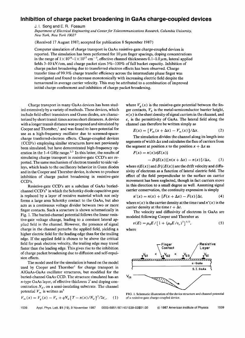
Resistive-gate CCD's are a subclass of GaAs buriedchannel CCD'S4 in which the Schottky diode capacitive gate is replaced by a layer of resistive material which not only forms a large area Schottky contact to the GaAs, but also acts as a continuous voltage divider between two or more finger contacts. Such a structure is shown schematically in Fig. I. The buried-channel potential follows the linear resistive-gate voltage change, leading to a constant lateral applied field in the channel. However, the presence of signal charge in the channel perturbs the applied field, yielding a higher electric field for the leading edge than for the trailing edge. If the applied field is chosen to be above the critical field for peak electron velocity, the trailing edge may travel faster than the leading edge. This gives rise to the inhibition of charge packet broadening due to diffusion and self-repulsion effects.
The model used for the simulation is based on the model used by Cooper and Thornber! for charge transport in AIGaAs-GaAs oscillator structures, but modified for the buried-channel GaAs CCD. The structure simulated has an n-type GaAs layer, of effective thickness T and doping concentration Nd' on a semi-insulating substrate. The channel potential Vm is written ass
Vm(x) = Vg(x) - Vb +qNd [T-n(x)/Nd ]212€s, (1)
where Vg (x) is the resistive-gate potential between the finger contacts, Vb is the metal-semiconductor barrier height, n (x) is the sheet density ofsignal carriers in the channel, and €s is the permittivity of GaAs. The lateral field along the channel can therefore be written simply as
E(x) = [Vm(x + ax) - Vm(x) ]/ax. (2)
The simulation divides the channel along its length into segments ofwidth ax and calculates the flux ofcarriers from the segment at position x to the position x + ax as
F(x) = n(x)v(E(x»)
- D(E(x»)[n(x + ax) - n(x) ]lax, (3)
where v(E(x») and D (E(x») are the drift velocity and ditfusivity of electrons as a function of lateral electric field. The effect of the field perpendicular to the surface on carrier movement has been neglected, though in fact carriers move in this direction to a small degree as well. Assuming signal carrier conservation, the continuity expression is simply
n'(x) =n(x) + [F(x+ax) -F(x)]at, (4)
where n (x) is the carrier density at the time t and n' (x) is the carrier density at the time t + at.
The velocity and diffusivity of electrons in GaAs are modeled following Cooper and Thornber as
v(E) =/1-0£/[1 + (/1-o£/vs)2] 1/2, (5)
where
FIG. 1. Schematic illustration of the device structure and channel potential of a resistive-gate charge-coupled device.
D(E) = Do + D, exp{ - [(In E -In E p )/lnA ]2} (7)
where Po is the low field electron mobility, Vs is the fielddependent saturation velocity, Do is the low field electron diffusivity, and VI' V2, E I , E 2, D, D I, Ep ' and A are empirical constants whose values are 4.77 X 107 cm/s, 3.24X 10⁷
The time step used in the simulation is initially set at 2.0 fs but is dynamically varied to optimize accuracy and computation time. The position step ax was fixed at 0.lL5 pm. Finger spacing was 10pm with finger widths ofone and zero microns. The effect of electric field was examined by using applied fields of 3, 4, 7, and 10kV/ cm. Channel thicknesses of O. I, 0.5, and 1.0 pm with doping concentrations of LOX 1016 and 1X 1017 cm -3 were simulated.
Initially, charge was assumed to be confined by three finger potentials such that the intermediate finger was held at a potential higher than the outer two, thereby confining the charge in a nearly triangular potential well. This results in a nearly triangular initial carrier distribution. The shnulation begins by changing the potential on the third electrode, giving rise to the situation depicted in Fig. 1.
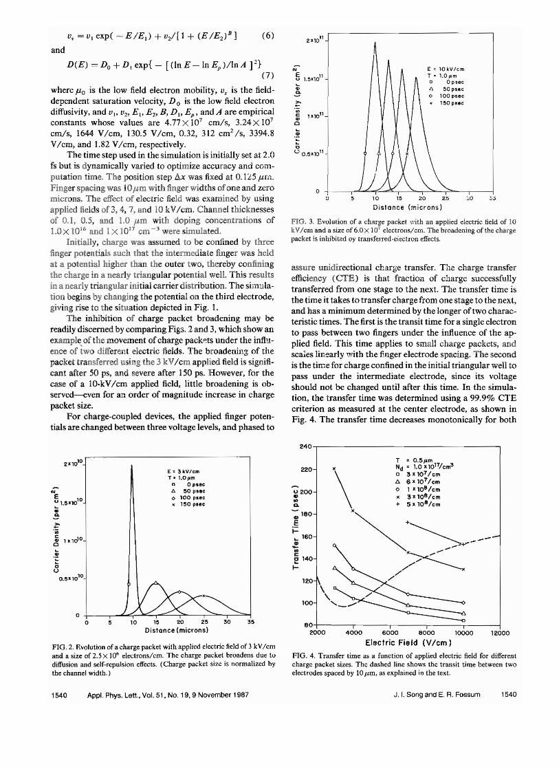
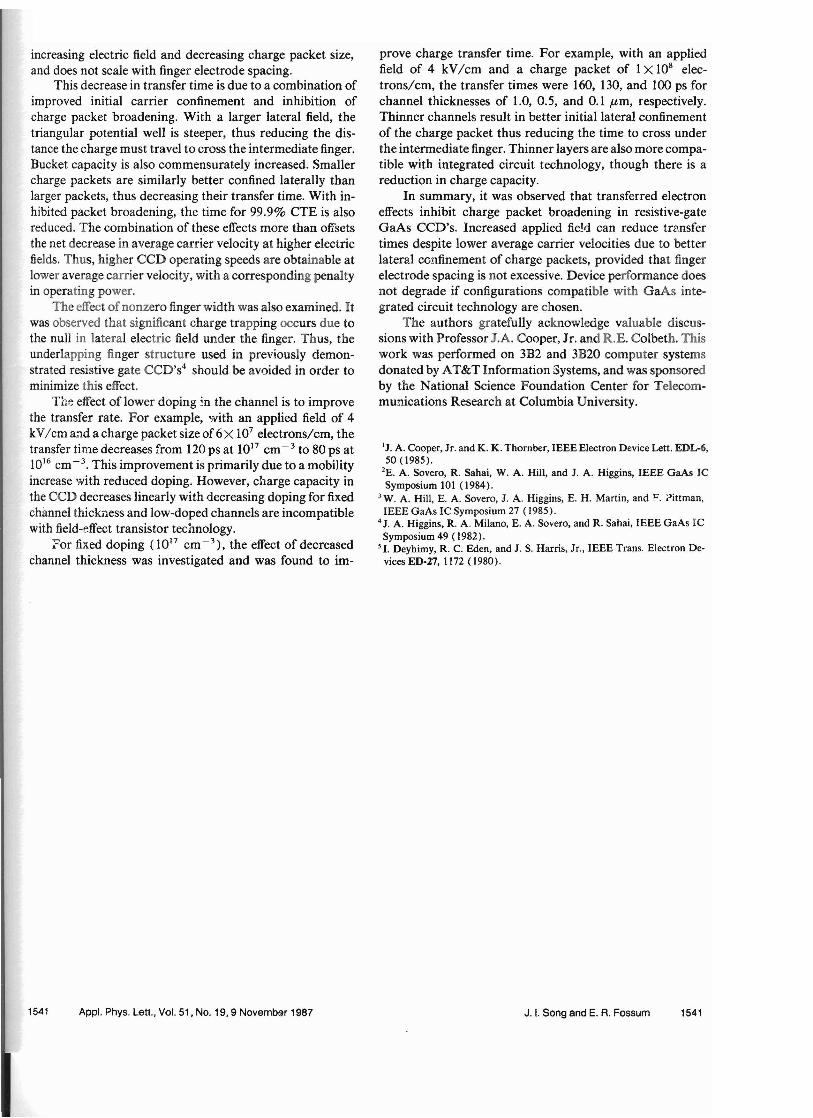
The inhibition of charge packet broadening may be readily discerned by comparing Figs. 2 and 3, which show an exampl~.of the movement of charge pack~ts under the influence of two different electric fields. The broadening of the packet transferred using the 3 kV/cm applied field is significant after 50 ps, and severe after 150 ps. However, for the case of a lO-kV/cm applied field, little broadening is observed---even for an order of magnitude increase in charge packet size.
For charge-coupled devices, the applied finger potentials are changed between three voltage levels, and phased to
Distance (microns)
FIG. 2. Evolution of a charge packet with applied electric field of 3 kV/crn and a size of 2.5 X 10⁶ electrons/em. The charge packet broadens due to diffusion and self-repulsion effects. (Charge packet size is normalized by the channel width.)
30
E = 10kV/em T' 1.01'm o 0 psec l> ~o p ••• o 100 p•••
~ 1~O P'••
10 15 20 25o
.. '" Q,
>0-
N E 11 u 1.5'10
Distance (microns)
FIG. 3. Evolution of a charge packet with an applied electric field of 10 kV/crn and a size of6.0X 107 electrons/em. The broadening of the charge packet is inhibited oy transferred-electron effects.
assure unidirectional charge transfer. The charge transfer efficiency (CTE) is that fraction of charge successfully transferred from one stage to the next. The transfer time is the time it takes to transfer charge from one stage to the next, and has a minimum determined by the longer of two characteristic times. The first is the transit time for a single electron to pass between two fingers under the influence of the applied field. This time applies to small charge packets, and scales linearly with the finger electrode spacing. The second is the time for charge confined in the initial triangular well to pass under the intermediate electrode, since its voltage should not be changed until after this time. In the simulation, the transfer time was determined using a 99.9% CTE criterion as measured at the center electrode, as shown in Fig. 4. The transfer time decreases monotonically for both
FIG. 4. Transfer time as a function of applied electric field for different charge packet sizes. The dashed line shows the transit time between two electrodes spaced by 10 fLrn, as explained in the text.
1540 Appl. Phys. Lett., Vol. 51, No. 19,9 November 1987 J. I. Song and E. R. Fossum 1540
increasing electric field and decreasing charge packet size, and does not scale with finger electrode spacing.
This decrease in transfer time is due to a combination of improved initial carrier confinement and inhibition of charge packet broadening. With a larger lateral field, the triangular potential well is steeper, thus reducing the distance the charge must travel to cross the intermediate finger. Bucket capacity is also commensurately increased. Smaller charge packets are similarly better confined laterally than larger packets, thus decreasing their transfer time. With inhibited packet broadening, the time for 99.9% CTE is also reduced. The combination of these effects more than offsets the net decrease in average carrier velocity at higher electric fields. Thus, higher CCO operating speeds are obtainable at lower average carrier velocity, with a corresponding penalty in operating power.
The effect ofnonzero finger width was also examined. It was observed that significant charge trapping occurs due to the null in lateral electric field under the finger. Thus, the underlapping finger structure used in previously demonstrated resistive gate CCO'S4 should be avoided in order to minimize this effect.
The effect of lower doping ;.n the channel is to improve the transfer rate. For example, with an applied field of 4 kV/ cm a:1d a charge packet size of 6X 10⁷ electrons/cm, the transfer time decreases from 120 ps at 1017 cm-3 to 80 ps at 1016 cm -3. This improvement is primarily due to a mobility increase with reduced doping. However, charge capacity in the CCO decreases linearly with decreasing doping for fixed channel thickness and low-doped channels are incompatible with field-effect transistor tecl1Dology.
Por fixed doping (10 17 cm- 3 ), the effect of decreased
channel thickness was investigated and was found to im
prove charge transfer time. For example, with an applied field of 4 kV/cm and a charge packet of 1X 10⁸ electrons/cm, the transfer times were 160, 130, and 100 ps for channel thicknesses of 1.0, 0.5, and 0.1 /-lm, respectively. Thinner channels result in better initial lateral confinement of the charge packet thus reducing the time to cross under the intermediate finger. Thinner layers are also more compatible with integrated circuit technology, though there is a reduction in charge capacity.
In summary, it was observed that transferred electron effects inhibit charge packet broadening in resistive-gate GaAs CCD's. Increased applied field can reduce transfer times despite lower average carrier velocities due to better lateral confinement of charge packets, provided that finger electrode spacing is not excessive. Device performance does not degrade if configurations compatible with GaAs integrated circuit technology are chosen.
The authors gratefully acknowledge valuable discussions with Professor I.A. Cooper, Jr. and R.E. Colbeth. This work was performed on 3B2 and 3B20 computer systems donated by AT&T Information Systems, and was sponsored by the National Science Foundation Center for Telecommunications Research at Columbia University.
'J. A. Cooper, Jr. and K. K. Thornber, IEEE Electron Device Lett. EDL-6, 50 (1985).
2E. A. Sovero, R. Sahai, W. A. Hill, and J. A. Higgins,. IEEE GaAs IC Symposium 101 (1984).
3 W. A. Hill, E. A. Sovero, J. A. Higgins, E. H. Martin, and !'. ?ittman, IEEE GaAs IC Symposium 27 (1985).
4 J. A. Higgins, R. A. Milano, E. A. Sovero, and R. Sahai, IEEE GaAs IC Symposium 49 (1982).
S I. Deyhimy, R. C. Eden, and J. S. Harris, Jr., IEEE Trans. Electron Devices ED-27, 1172 (1980).
1541 Appl. Phys. Lett., Vol. 51, No. 19,9 Novemb$r 1987 J. I. Song and E. R. Fossum 1541