29
TECHNOLOGY INNOVATIONS IN PV MANUFACTURING DR. A TUL GUPTA, DIRECTOR R&D/PRODUCT DEVELOPMENT

TECHNOLOGY INNOVATIONS IN PV MANUFACTURING DR. ATUL GUPTA,
DIRECTOR R&D/PRODUCT DEVELOPMENT

Suniva overview
Our approach to innovations
– Why, what and how?
– Innovating through tough times
– Key challenges
– Technology options
Impact on Metrology Equipment Makers
2
OUTLINE

WHO WE ARE
Manufacturer/developer of high-efficiency, crystalline silicon PV cells & modules
– High-Efficiency Cells: Averaging 19+% in production; over 20% in pilot; roadmap to over 22% by 2015
– High-Power Modules: 16+% in production; 60 cell modules up to 270W, 72-cell modules up to 315W
– Deep R&D Capabilities: In-house cell and module labs; collaboration with UCEP at Georgia Tech
– Cost Competitiveness: Cost competitive with top-tier Asian manufacturers, with higher quality
– Manufacturing Capacity: 170 MW in the U.S.; 500 MW in Asia
– Buy America Compliant Modules: one of the highest U.S.-content modules on the market
– Market focus: Commercial, residential and utility applications in the U.S., Asia and Europe
3
Investor Backing:

4
SUNIVA® INNOVATION IN THE VALUE CHAIN
Silicon Ingot Wafer Systems Integrators
Cells Modules
Balance of System Solutions
Unique Partnerships
The solar cell is the “DNA” of
any PV system, and hence the key driver of value

Making high-quality, high-power solar cells and
modules using U.S.-based technology at
affordable costs to address the world’s energy needs
NEW TECHNOLOGY INNOVATIONS

KEY ELEMENTS FOR INNOVATION
Innovation
Need/Desire to innovate
Foundational principle
Visionary leadership
Knowhow + capability
Deep technical expertise
Solid financial backing
Infrastructure
Fully equipped R&D lab
Access to GT equipment
Access to Pilot Production line
Access to new technologies
Multiple collaborations
Successful track record
6

7
Deep Roots, Continued Collaboration
Suniva has access to over $50M worth of advanced research equipment at UCEP/Georgia Tech
Suniva benefits from a budget of over $43M of PV-related research programs funded partly by the U.S. DOE
90 kW rooftop installation on Georgia Tech’s Clough Center 90 kW rooftop installation on Georgia Tech’s Clough Center
1985: PV Program Established at Georgia Tech
Department of Energy
provided funding
1992: University Center of
Excellence Established
2007: Suniva Founded
Dr. Ajeet Rohatgi Suniva Founder & CTO
Distinguished Professor of Electrical Engineering at Georgia Tech
John H. Weitnauer, Jr. Chair Georgia Research Alliance Eminent
Scholar 16 world-record cells 42 patent families 400+ publications Westinghouse Engineering
Achievement Award IEEE Cherry Award, 2003 NREL Rappaport Award, 2003 5 Most Influential in Renewable
Energy, 2008 Named “Champion of PV”, 2010

Q. Which Ones to Pursue?
A. Varies, based on where you are in the value chain!
Lower $ (@same performance) for Materials Suppliers
Lower $/Wp (cells/panels) for Cell/Module makers
Lower $/Wp (Installed system cost) for System Installers
Lower LCOE for EPCs
8
TECHNOLOGY INNOVATIONS

New Technologies need to support the declining module based on the learning curve (~21% for every doubling of capacity)
SURVIVING AS A PANEL MANUFACTURER
Source : ITRPV 2013
9

Solar Photovoltaic Module Revenues to Rebound to $32 Billion by 2017, According to NPD Solarbuzz
Solar Photovoltaic Demand to Reach 31 Gigawatts in 2013, According to NPD Solarbuzz
Solar Photovoltaic Demand in 2012 Falls Short of 30 GW Mark, Reports NPD Solarbuzz
World Solar Photovoltaic Market Grew to 27.4 Gigawatts in 2011, Up 40% Y/Y
10
WHAT SHOULD WE PLAN FOR?
Plan for the Module Prices to decline (21.5% for every doubling of installed capacity) despite recent reports of recovery and growing demand
Module manufacturers should plan for a $0.03 to $0.05/Wp annual decline in ASPs over the next 2-5 years
Simple MATH : 2012 installed capacity ~110GW , installation rate ~31GW/year 2012 ASP ~0.70/Wp ~3 years to double installed capacity $0.70/Wp$0.55/Wp (21.5% decline) (=$0.05/Wp Annual Decline!)

A. Two (usually conflicting) approaches!
11
HOW DO WE GET THERE?
Lower the Cost of Manufacturing
Get Higher Performance

1. Lower cost materials
1. Cheaper polySi, thinner Wafers, cheaper glass/EVA/frame etc.,
2. Eliminate non-value add steps
1. Junction Isolation, Extra Cleans (wafering/cell processing), co-anneals etc.
3. Improved manufacturing yields/Tighter Process Control
1. BatchSemibatch wet processing, SPC, inline metrology etc.
4. Improved tool/factory utilization
1. WIP management, Fab Automation, 2x loading, larger PECVD boats, etc.
5. Lower cost of ownership
1. Lower material usage per wafer (Ag paste etc.) , solar grade materials
12
LOWERING THE COST OF MANUFACTURING

1. Generate More : Let More Light Into the Absorber
1. Cell level : Improve texturing, optimize ARC, improve back surface reflectance, minimize front grid shading
2. Module Level : AR Glass, high Transparency EVA, improved back reflector
2. Lose Less : Reduce Recombination Losses
1. Higher Lifetime material
2. Improved Emitter technology (Lighter doping), e.g. Implant or High Rsheet POCl3 processes
3. Improved Passivation Process (less Surface recombination): Oxide/SiNx stacks or AlOx/SiNx stack, reduced Metal contact
3. Collect More : Reduce Resistive Losses
1. Optimize Front Grid/BBR configuration (Increase as technology matures)
2. Higher Conductivity Interconnect Ribbons
13
INCREASING CELL/MODULE EFFICIENCY

INNOVATIONS IN CELL TECHNOLOGY
2008
Eff
icie
ncy
< 6months Startup
Industry leading performance
2-bus bar cell design
Proprietary recipes
Process optimization
Material and equipment improvements
3-bus bar design
ARTisun Select 19.0%
ARTisun Star
>20%
Advanced Metallization
Finer Gridlines
Higher efficiency at Lower Cost
ARTisun Select + 19.5%
Proprietary >20% cell structure
Back side improvements
NREL certified over 20%
Proprietary Cell and Process
World’s First adopter of Implant
Front side emitter improvement
Process Simplification
ARTisun 18.0%
ARTisun 17%
ARTisun Select 19.0%
ARTisun Star 20% ARTisun
Select + 19.5%
Execution Optimization Innovation Simplification Collaboration
Current Production Pilot Validation
20.4% in LAB
N-type substrate
Back contact eliminates all shading
Integrated front & back side enhancements
Simplified 12-step process
ARTisun IBC
> 22%
14

ADVANTAGES OF ION-IMPLANTATION
Higher Performance (gained 1% abs. in cell efficiency)
– Formation of high quality emitter with no dead layer
– Enables high quality passivation through in-situ oxidation during anneal step
– Simple and better controlled process enables tighter binning of high value product from the line
Lower Costs due to Process Simplification :
– Elimination of non-value add steps like edge isolation and dopant glass removal
– Improved Yields (gained 2% in overall yield by eliminating edge isolation)
Strategic Fit (access to advanced device structures)
– Enables low cost Boron doping solution
– Compatible with Patterned implantation for advanced device structures
15
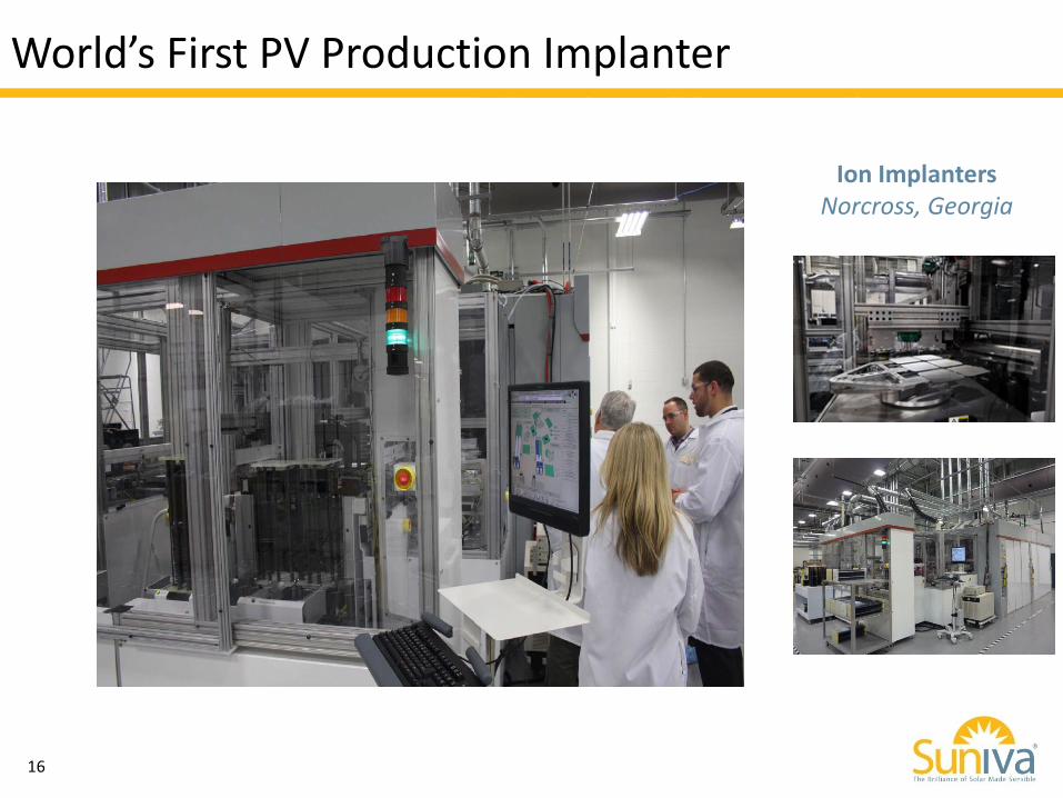
World’s First PV Production Implanter
Ion Implanters Norcross, Georgia
16

PERFORMANCE DISTRIBUTION FROM A TYPICAL DAILY PRODUCTION RUN AT SUNIVA
0
5000
10000
15000
20000
25000
30000
18.7% 18.8% 18.9% 19.0% 19.1% 19.2% 19.3% 19.4% 19.5% 19.6%
Nu
mb
er
of
Ce
lls
Staying Ahead of the pack is critical to have high factory utilization
17

Minimize Material Costs In Cell Processing
– Particularly Front Ag pastes (~45% of materials) through Screen Optimization
18
NEXT STAGE OF EVOLUTION

The Optimum Screen for Efficiency is more expensive than the one optimized for lowest $/Wp
19
OPTIMIZING FRONT PATTERNS
Max. Efficiency
Lowest $/Wp
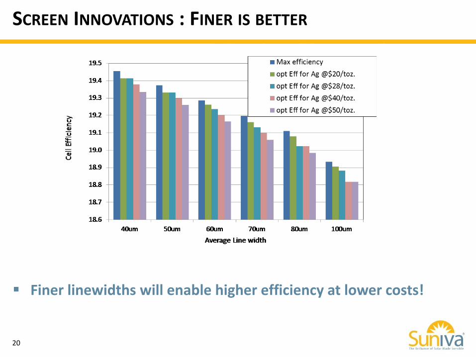
Finer linewidths will enable higher efficiency at lower costs!
20
SCREEN INNOVATIONS : FINER IS BETTER

Advanced cell designs need additional processing steps (increased cell conversion costs) that needs to be offset by efficiency gains
Falling Cell/Module Prices reduce this leverage making adoption harder!
WHAT ABOUT HIGHER EFFICIENCY DESIGNS?
Increased conversion cost/ wafer
Wafer + Cell Processing + Module BOM
New Technologies Must Eliminate “non-value add” steps or “accomplish more with less”
21

PERC cell on p-type substrate (In Pilot validation)
Key Elements
1. Improved Back passivation
2. Back reflector (Cheap coating)
3. Local contact formation (Ablation or LFC)
22
NEXT GENERATION CELL TECHNOLOGY

23
CHALLENGES IN MODULE MANUFACTURING
1. Reliability – Supports a 25 Year Service Life (and beyond) 2. Bankability – Independent Verification of Reliability 3. Cost – Both Initial and LCOE 4. Performance – As it contributes to cost and competitiveness

SUNIVA’S ENHANCED TEST PROTOCOLS
24
Ensure safety and reliability of products
Demonstrate long-term module performance
Validate new cell designs & materials
Ensure we incorporate new materials
without a higher risk of reliability failures
Validate changes in process specifications
Tier 1 Competitors
UL1703 Safety Standard
IEC 61215 Performance Standard
IEC 61215 Performance Standard
Fraunhofer Extended Reliability Tests
(In addition to IEC and UL!)
UL1703 Safety Standard
Suniva Material
Qualification (In addition to UL, IEC and
Fraunhofer!)
On-going Suniva module lab
quality and reliability testing of sample production

Why we do testing!
Examples of Product Failures
Failure: This sample failed after only 300 hours in the damp heat chamber
Hidden Cracks leading to EVA discoloration: AKA Snail Trail
Example of a PV module with burnt diode
Cell Hot Spots Causing Burn Marks Cell Current Mismatch Mechanical Load Failure
25 Industry needs Reliable and Faster measurements/tests

Confidential & Proprietary © Suniva®, Inc. 2012
26
MODULE INNOVATIONS : MATERIAL COST REDUCTION

Success of a Solar Cell/panel Manufacturer is contingent upon continued innovations in technology/manufacturing
– Ability to simplify processes and remove redundant steps with Innovative processing technologies
– Cost optimization/reduction without compromising quality and reliability is the key requirement for success in this industry
New Device Technologies need to accomplish more for adoption
– Shrinking lever of wafer and module BOM costs
– Focus on technologies/processes that give “2 for 1”
27
SUMMARY
Collaborative Development Efforts between Equipment and Cell/panel manufacturers are Required to Ensure Adoption

Near Term
1. Universal IV testing
2. Full wafer characterization
3. Cosmetics/Quality specs
Longer Term
1. Integrated tool level SPC
2. Defect characterization and root cause analysis
3. Materials qualifications
28
OPPORTUNITIES FOR METROLOGY COMPANIES
Near Term
1. Interconnect ribbon reliability
2. Optimized matching of cells during stringing/assembly
3. 100% EL/PL inspection
Longer Term
1. Accelerated reliability testing
2. Warranty rating for each module
MODULE MANUFACTURING CELL MANUFACTURING

29


