Integrable Tunable Laser Assembly Multi Source Agreement OIF-ITLA-MSA-01.3 July 13 th , 2015 Implementation Agreement created and approved by the Optical Internetworking Forum www.oiforum.com
Transcript
Integrable Tunable Laser Assembly Multi Source Agreement
OIF-ITLA-MSA-01.3
July 13th, 2015
Implementation Agreement created and approved by the Optical Internetworking Forum
www.oiforum.com
www.oiforum.com 2
The OIF is an international non profit organization with over 100 member companies, including the world’s leading carriers and vendors. Being an industry group uniting representatives of the data and optical worlds, OIF’s purpose is to accelerate the deployment of interoperable, cost-effective and robust optical internetworks and their associated technologies. Optical internetworks are data networks composed of routers and data switches interconnected by optical networking elements. With the goal of promoting worldwide compatibility of optical internetworking products, the OIF actively supports and extends the work of national and international standards bodies. Working relationships or formal liaisons have been established with CFP-MSA, COAST, Ethernet Alliance, Fibre Channel T11, IEEE 802.1, IEEE 802.3, IETF, InfiniBand, ITU-T SG13, ITU-T SG15, MEF, ONF, Rapid I/O, SAS T10, SFF Committee, TMF and TMOC.
For additional information contact:
The Optical Internetworking Forum, 48377 Fremont Blvd, Suite 117, Fremont, CA 94538
Notice: This Technical Document has been created by the Optical Internetworking Forum (OIF). This document is
offered to the OIF Membership solely as a basis for agreement and is not a binding proposal on the companies listed as
resources above. The OIF reserves the rights to at any time to add, amend, or withdraw statements contained herein. Nothing in this document is in any way binding on the OIF or any of its members.
The user's attention is called to the possibility that implementation of the OIF implementation agreement contained herein
may require the use of inventions covered by the patent rights held by third parties. By publication of this OIF implementation agreement, the OIF makes no representation or warranty whatsoever, whether expressed or implied, that
implementation of the specification will not infringe any third party rights, nor does the OIF make any representation or warranty whatsoever, whether expressed or implied, with respect to any claim that has been or may be asserted by any
third party, the validity of any patent rights related to any such claim, or the extent to which a license to use any such
This document and translations of it may be copied and furnished to others, and derivative works that comment on or otherwise explain it or assist in its implementation may be prepared, copied, published and distributed, in whole or in
part, without restriction other than the following, (1) the above copyright notice and this paragraph must be included on
all such copies and derivative works, and (2) this document itself may not be modified in any way, such as by removing the copyright notice or references to the OIF, except as needed for the purpose of developing OIF Implementation
Agreements.
By downloading, copying, or using this document in any manner, the user consents to the terms and conditions of this notice. Unless the terms and conditions of this notice are breached by the user, the limited permissions granted above are
perpetual and will not be revoked by the OIF or its successors or assigns. This document and the information contained herein is provided on an “AS IS” basis and THE OIF DISCLAIMS ALL
WARRANTIES, EXPRESS OR IMPLIED, INCLUDING BUT NOT LIMITED TO ANY WARRANTY THAT THE USE OF
THE INFORMATION HEREIN WILL NOT INFRINGE ANY RIGHTS OR ANY IMPLIED WARRANTIES OF MERCHANTABILITY, TITLE OR FITNESS FOR A PARTICULAR PURPOSE..
Integrable Tunable Laser Assembly Multi Source Agreement
www.oiforum.com 3
1 Table of Contents 1 Table of Contents ................................................................................................................. 3 2 List of Tables ........................................................................................................................ 6 3 List of Figures....................................................................................................................... 7 4 Document Revision History .................................................................................................. 8 5 References and Conventions.............................................................................................. 13
5.1 External Reference Documents ................................................................................... 13 5.2 Conventions Used in This Document ........................................................................... 13
9.9 Manufacturer Specific (0x80-0xFE) .............................................................................. 94 10 Alarm and Status Register Behavior ................................................................................ 95
10.1 Introduction .............................................................................................................. 95 10.2 StatusF/StatusW Register Definitions ....................................................................... 95 10.3 Status Bit Determination Conditions and Behavior .................................................... 96 10.4 Effects of Alarm During Tuning (ADT) bit in MCB register (0x33) .............................. 98
11.1.1 Optical Parameter Definitions ............................................................................. 100 11.1.1.1 Frequency Tuning Range ............................................................................ 100 11.1.1.2 Fiber Output Power ..................................................................................... 100 11.1.1.3 Output Power Variation Across Tuning Range ............................................. 100 11.1.1.4 Frequency Error to the ITU Grid ................................................................... 100
OIF-ITLA-MSA-01.3
Integrable Tunable Laser Assembly Multi Source Agreement
11.2 Timing Specifications ............................................................................................. 105 11.3 Module Warm Up Time .......................................................................................... 105 11.4 Frequency and Optical Power Transient Specifications .......................................... 105
13 Important Editorial Changes in OIF-ITLA-MSA-01.3 ...................................................... 110 13.1 Purpose of this Appendix ....................................................................................... 110 13.2 High Resolution Frequency Control Registers ........................................................ 110 13.3 Register Value Error Checking for High Resolution Registers ................................. 110 13.4 Anomolous Behaviour of Certain Registers on RVE Condition ................................ 111
14 Appendix A: Open Issues / Current Work Items ............................................................. 111 15 Appendix B: List of Companies and Contributors ........................................................... 111
15.1 Technical Contributors (to the Original Document).................................................. 111 15.2 List of OIF Member Companies (at time of adoption) .............................................. 112
16 Document Index ............................................................................................................ 113
OIF-ITLA-MSA-01.3
Integrable Tunable Laser Assembly Multi Source Agreement
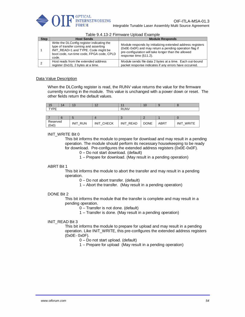
(Grid) to include FTF setting, and scaled all units in equation to GHz. Added FTFR register (0x4F) in Table 9.2. Added Section 9.7.1, FTFR (0x4F) register.
Added Section 11.4, frequency and optical power transient specifications Fixed row numbering in Table 6.4.2-2. Fixed row numbering in 9.4.2.
Corrected data value description in Section 9.5.4 from 0x25/0x24 to 0x27/0x26.
Updated index reference in Section 9.4.1, for MRDY bit in NOP register. Updated electrical connectors to CLM-107-02-H-D-K-TR and ASP-124330-02 in Section 7.1.1 and 12.
Added 2mm minimum bend radius to mechanical drawing in Section 12.1. Added protocol version and up revision to 2.0.0 on Page 12. Revised PV version number in example in Section 9.4.7. Release register to 2.0.0
Deleted CRC-16 section and all references to [W/R]CRC as command had been deprecated in previous release. Removed User Data Storage (0xFF) register as command was deprecated
in previous release. Removed Lock register (0x16) and all references to lock. Fixed typo in Section 9.6.6 (FCF1/FCF2) where text referred incorrectly to
LF1/2 when it should be FCF1/2. Added Section 10 describing the behavior of alarm and status registers.
Modified all references to ALM* and FATAL* to either pointing to software bits ALM, FATAL respectively or removing reference as hardware lines do not exist in this MSA (only in tunable laser MSA).
Modified Sections 9.5.7 (ALMT) and 9.6.4 (MCB) recommendation from 0x0504 to 0x0700 as fatal bits do not assert during tuning. Clarified DLStatus 9.4.14 to state that IS_VALID is set once both TYPE and
INIT_CHECK are asserted. Statement added : “and with "INIT_CHECK" equal to 1.” Removed non-volatile support for gencfg register as CRC-16 no longer
supported. See Section 9.2 and 9.4.9. Clarified that Laser Age can be a trigger condition in the alarms (Section
9.5.1). Removed text: “This is latched and cleared by SENA. “ in Sections 9.6.1 and 9.6.3 also changed “Note that changing the DIS* pin to high will not
cause a tune” to “Note that changing the DIS* pin to high will not re-enable the output.” Clarified Digital Dither Enable as 1 bit in Section 9.8.3.
Corrected SRQT register value in Synopsis from 0x26 to correct value 0x28. Added word “Suggested:” to default content values for SRQT, ALMT, FATALT as these registers have manufacturer specific default values.
Removed manufacturer specific for 9.6.4 (MCB). It is now default. Value is 0x02 In Channel, made | to || ((Fatal_Status & Fatal_Trigger) && SDF) || ~SENA
|| ~DIS and in RESENA register. Removed invalid references in ITLA-MSA-01.1 revision history. References
were made to deprecated commands and no longer valid as they have been removed. Clarified that the PWR command can have variable adjustment and that CIE
is issued when tuned if command is traffic interrupting. Add the logical operators and bitwise operators to the “Conventions Used in this Document” section.
Moved LstRsp bit to be part of transport layer to be self-consistent in Section 9.1.1 In-Bound (Host to Module). Corrected typo in Table 7.1.2-2 that Pins 1,3 are tied together on 3.3V line
instead of pins 1,2.
Corrected typo in Figure 8.1-3 where 28 bits were referred to
when actually 27 bits (26:0) are to be framed. Corrected typo in Table 9.1-1 where status bits were incorrectly
referenced as bits 1:0 instead of 25:24.
OIF-ITLA-MSA-01.3
Integrable Tunable Laser Assembly Multi Source Agreement
www.oiforum.com 10
OIF-ITLA-MSA-01.3 10th
May 2014 Maintenance activity to add additional optional registers which enable
higher resolution to be handled in the firmware. Registers added run from 0x63 through to 0x6B. Register names are FFreqTh2, WFreqTh2, ChannelH, GRID2, FCF3, LF3, LFL3, LFH3, LGrid2. Additional examples
are added in the section dealing with ChannelH to help identify the use and effect of the new register.
The additional registers enable the firmware to handle a resolution of 1MHz.
It should not be assumed that the hardware implementation is necessarily
capable of this. Check with the ITLA vendor. The changes facilitate operation of the ITLA firmware interface on flexible grid or fine grid applications.
When high resolution registers are provided the Protocol Version is raised to PV 3.0.0
In 9.7.1 Fine Tune Frequency Range (FTF 0x4F)[R] is corrected to (FTFR
0x4F)[R]
In section 9.6.1 and 9.6.7 the equation to calculate frequency is corrected to
reference the correct hex address for the FTF register, i.e FTF(0x62/1000) and not FTF(0x4F/1000)
OIF-ITLA-MSA-01.3 30th
May 2014 Changes from the 10th
May 2014 have been accepted. Additional edits are
added to respond to oif2014.195.00 of 21st May 2014. These changes were
raised at the Q2 Technical Meeting 2014 (Berlin).
OIF-ITLA-MSA-01.3
Integrable Tunable Laser Assembly Multi Source Agreement
www.oiforum.com 11
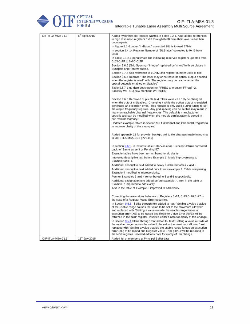
OIF-ITLA-MSA-01.3 5th
April 2015 Added hyperlinks to Register Names in Table 9.2-1. Also added references
to high resolution registers 0x63 through 0x6B from their lower resolution counterparts.
In Figure 8.1-3 under “In-Bound” corrected 28bits to read 27bits.
In section 9.4.14 Register Number of “DLStatus” corrected to 0x15 from
0x08
In Table 9.1.2-1 penultimate line indicating reserved registers updated from
0x63-0x7F to 0x6C-0x7F
Section 9.6.5 (Grid Spacing) “integer” replaced by “short” in three places in
Synopsis and Returns tables.
Section 9.7.4 Add reference to LGrid2 and register number 0x6B to title.
Section 9.6.7 Replace “The laser may or not have its optical output enabled
when the register is read” with “The register may be read whether the optical output is enabled or disabled”
Table 9.8.7-1 up-date description for FFREQ to mention FFreqTh2. Similarly WFREQ now mentions WFreqTh2.
Section 9.6.5 Removed duplicate text. “This value can only be changed
when the output is disabled. Changing it while the optical output is enabled generates an execution error. This register is only used during tuning to set the output frequency register. Any grid spacing can be set but may result in
many unreachable channel frequencies. The default is manufacturer specific and can be modified when the module configuration is stored in non-volatile memory.”
Updated example tables in section 9.6.1 (Channel and ChannelH Registers)
to improve clarity of the examples.
Added appendix 13 for provide background to the changes made in moving
to OIF-ITLA-MSA-01.3 (PV3.0.0)
In section 9.6.1. In Returns table Data Value for Successful Write corrected
back to “Same as sent or Pending ID”
Example tables have been re-numbered to aid clarity.
Improved descriptive text before Example 1. Made improvements to
Example table 1.
Additional descriptive text added to newly numbered tables 2 and 3.
Additional descriptive text added prior to new example 4. Table comprising
Example 4 modified to improve clarity.
Former Examples 3 and 4 renumbered to 5 and 6 respectively.
Additional explanation text added before Example 7. Text in the table of
Example 7 improved to add clarity.
Text in the table of Example 8 improved to add clarity.
Correcting the anomalous behavior of Registers 0x24, 0x25.0x26,0x27 in
the case of a Register Value Error occurring.
In Section 9.5.3. Strike through font added to text “Setting a value outside
of the usable range causes the value to be set to the maximum allowed” and replaced with “Setting a value outside the usable range forces an
execution error (XE) to be raised and Register Value Error (RVE) will be returned in the NOP register. Inserted editor’s note for clarity of this change.
In Section 9.5.4 Strike through font added to text “Setting a value outside of the usable range causes the value to be set to the maximum allowed” and
replaced with “Setting a value outside the usable range forces an execution error (XE) to be raised and Register Value Error (RVE) will be returned in the NOP register. Inserted editor’s note for clarity of this change.
OIF-ITLA-MSA-01.3 13th
July 2015 Added list of members at Principal Ballot date
OIF-ITLA-MSA-01.3
Integrable Tunable Laser Assembly Multi Source Agreement
Project Name: Integrable Tunable Laser Assembly MSA (ITLA-MSA) Project Number: OIF-0013 Project Abstract: This contribution contains the updated changes to MSA-IA-01.0 for the
Integrable Tunable Laser Assembly (ITLA) for integration into a 300-pin 3.5”x4.5” transponder. The changes incorporated are from oif2005.128.04 as approved in the technical committee principal ballot oif2005.372.00.
The maintenance activity adds the provision of high resolution registers and raises the protocol version to 3.0.0.. See Document Revision History.
Integrable Tunable Laser Assembly Multi Source Agreement
www.oiforum.com 13
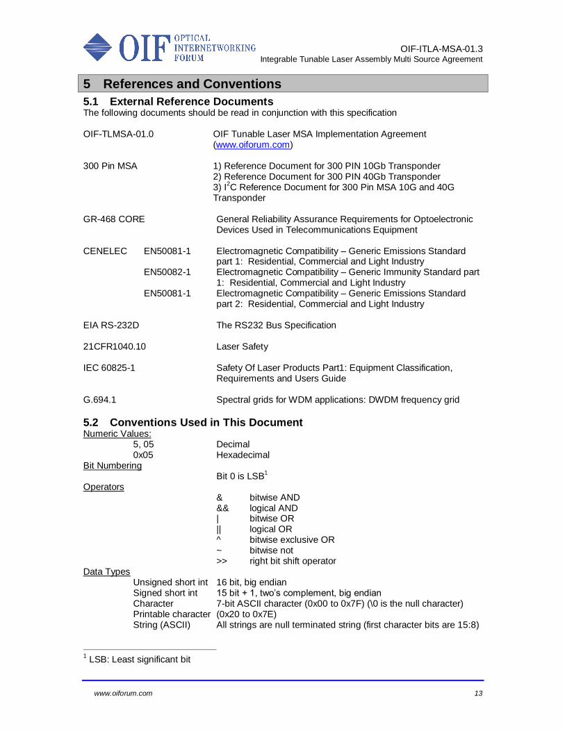
5 References and Conventions
5.1 External Reference Documents The following documents should be read in conjunction with this specification OIF-TLMSA-01.0 OIF Tunable Laser MSA Implementation Agreement
2) Reference Document for 300 PIN 40Gb Transponder 3) I
2C Reference Document for 300 Pin MSA 10G and 40G
Transponder GR-468 CORE General Reliability Assurance Requirements for Optoelectronic
Devices Used in Telecommunications Equipment CENELEC EN50081-1 Electromagnetic Compatibility – Generic Emissions Standard
part 1: Residential, Commercial and Light Industry EN50082-1 Electromagnetic Compatibility – Generic Immunity Standard part
1: Residential, Commercial and Light Industry EN50081-1 Electromagnetic Compatibility – Generic Emissions Standard
part 2: Residential, Commercial and Light Industry EIA RS-232D The RS232 Bus Specification 21CFR1040.10 Laser Safety IEC 60825-1 Safety Of Laser Products Part1: Equipment Classification,
Requirements and Users Guide G.694.1 Spectral grids for WDM applications: DWDM frequency grid
5.2 Conventions Used in This Document Numeric Values:
5, 05 Decimal 0x05 Hexadecimal
Bit Numbering Bit 0 is LSB
1
Operators & bitwise AND && logical AND | bitwise OR || logical OR ^ bitwise exclusive OR ~ bitwise not >> right bit shift operator
Data Types Unsigned short int 16 bit, big endian Signed short int 15 bit + 1, two’s complement, big endian Character 7-bit ASCII character (0x00 to 0x7F) (\0 is the null character) Printable character (0x20 to 0x7E) String (ASCII) All strings are null terminated string (first character bits are 15:8)
Integrable Tunable Laser Assembly Multi Source Agreement
www.oiforum.com 14
Data Direction Out-bound Module to host transfer (Response packet) In-bound Host to module transfer (Command from host)
Module Module Refers to the integrable assembly as a module.
Transponder Base Portion of housing to which external heat sink is attached Lid Portion of housing with opening for 300 pin connector
OIF-ITLA-MSA-01.3
Integrable Tunable Laser Assembly Multi Source Agreement
www.oiforum.com 15
6 Introduction
6.1 Scope This document is a Multi-Source Agreement for integrable tunable laser assemblies. It details a communication protocol, electrical interface, power supply, optical specifications, and a mechanical interface for use in telecommunications equipment operating in the C or L band.
6.2 Background The OIF has completed two tunable laser projects. The first project resulted in the Tunable Laser Implementation Agreement, OIF-TL-01.1 began in April 2001 and was released in November 2002. A large number of contributors from a wide variety of consumers and suppliers of tunable lasers were involved in contributing and reviewing the first Implementation Agreement. It addressed the communication protocol, electrical interface and mechanical form factor interoperability for tunable continuous wavelength (CW) lasers. The document serves as a roadmap for future tunable device implementation agreements. In February 2003, the OIF began a new fast track project, the Tunable Laser MSA Implementation Agreement. This MSA-IA builds upon the existing Tunable Laser Implementation Agreement, generating a more comprehensive specification of the optical, electrical, mechanical, and communication protocols. It was completed in May 2003. In October 2003, the OIF began a new project, the Integrable Tunable Laser Assembly (ITLA) MSA Implementation Agreement to focus on standardization of a CW laser subassembly for integration into transponders for both the 3.5”x4.5” transponder as well as the small form factor transponder.
The OIF-IAs can be found at www.oiforum.com as document OIF-TL-01.1.pdf at http://www.oiforum.com/public/documents/OIF-TL-01.1.pdf and OIF-TLMSA-01.0.pdf at http://www.oiforum.com/public/documents/OIF-TLMSA-01.0.pdf.
Integrable Tunable Laser Assembly Multi Source Agreement
www.oiforum.com 16
6.3 Communication Overview The following diagram (Figure 6.3-1) depicts the communication process.
Figure 6.3-1 Three Layer Communication Diagram
Assume the host has a request to transmit to the module (Host’s Request). The request is first encoded as a 28-bit command packet in the Host Driver’s application layer. The command is then framed as a 32-bit packet in the host driver’s transport layer. The framing operation includes the addition of a BIP-4
2 checksum. Finally, the host driver’s
physical interface (RS232 shown) encodes the 32 bit packet as 4 ten bit3 RS232
“characters” and transmits in across the TxD line to the module. The module’s physical layer receives 40 bits and de-codes them by removing the RS232 start and stop bits. The resulting 32-bit frame is delivered to the transport layer where checksum is checked for consistency. Assuming no error is generated, the 28-bit command packet is delivered to the module’s application layer where the command is decoded and executed. The command execution will generate a response when complete
4. The response packet
consists of 26 bits. The response packet is delivered to the module’s transport layer which frames the packet by pre-pending a checksum, communication error (CE). The resulting 32-bit packet is then delivered to the module’s physical layer where it is then encoded as 40 bits.
2 Bit Interleaved Parity (4 bits)
3 Note each byte to be transmitted by RS232 is encapsulated by a start and stop bit thus pre-
pending 1 bit and post-pending 1 bit for a total of 10 bits for each byte to be transmitted. 4 Note that an initial response may also be generated for commands whose execution time
exceeds the command response timeout period. The host can either poll for completion of the command or have pre-configured the module to issue a service request (SRQ) upon completion of the command.
OIF-ITLA-MSA-01.3
Integrable Tunable Laser Assembly Multi Source Agreement
www.oiforum.com 17
The host then receives the 4 RS232 characters and performs the inverse operations as the packet moves up the host’s layer hierarchy.
6.3.1 Physical Interfaces
The communications interface supports only one physical layer protocol, RS232.
6.4 Command Overview The commands to the module consist of a 9-bit operation followed by 2 bytes of optional data. Alternatively, the command can be thought of as one read/write bit followed by an 8-bit register number followed by 2 bytes of optional data. See Figure 6.4-1. The register paradigm will be used in this document.
Figure 6.4-1: Paradigms for Module Control
Command Paradigm 9 bit command Data byte 1 Data byte 2
Register Paradigm Read/Write Bit 8 bit register
number Data byte 1 Data byte 2
There are 256 directly accessible registers (0x00 to 0xFF) in the primary register address space. The OIF-IA allocates the first 32 registers (0x00 to 0x1F) for generic module operations for all module types. Another 96 registers (0x20-0x7f) are reserved for device type “CW Laser Int Assy”. Finally, the remaining 128 registers (0x80-0xFF) are provided as manufacturing specific registers. The following example shows how the module’s status would be read.
Table 6.3.1-1: Example Reading Module Status
#
Command (Host to Module) Response (Module to Host)
Note: Example shows that the module status is 0x0000 as returned in the response data.
6.4.1 Command Execution Overlap
The application layer provides support for pending operations especially useful for operations that can take a significant period of time to complete
5.
If a command is issued to the module that results in a long time to complete, the module will return a response packet within the specified time out period for the module and flag the operation as pending
6. The interface is now free to respond to additional commands.
The host can determine when the pending operation completes by polling the NOP register (0x00). The NOP register returns the pending operation status as well as any error conditions. Note that the module can be configured to generate an SRQ (Service Request) when a pending operation terminates operation in an error state. See §9.4.1 and §9.1.2.
.
5 Channel tuning is an example of a command which can take from 5ms to 15s to achieve
depending on laser technology utilized. 6 Some other interfaces such as the 300-pin transponder MSA do not allow command execution
overlap.
OIF-ITLA-MSA-01.3
Integrable Tunable Laser Assembly Multi Source Agreement
www.oiforum.com 18
6.4.2 Extended Addressing
Extended addressing provides an additional memory space (22 address bits) in addition to the primary 256 registers (8-bit address space). The extended addressing feature consists of three registers described in Table 6.4.2-1.
Configuration Defines basic configuration for the extended address
Defines the address space
high order address bits
Address Address of field in either physical or virtual memory space
Defines the 16 low order address bits
Contents
Reading from this register returns data
stored in this field 16 bits at a time Write to this register stores data into this
field 16 bits at a time
16 bit data value
Once the configuration and address registers are configured, the host may issue a series of read or write commands to the (indirect contents register) thereby accessing the memory location pointed to by the indirect register. The locations may map to physical or virtual memory spaces. The configuration register and address registers are usually pre-configured when one of the primary registers is accessed which holds an object longer than a 16-bit integer. For example, the device type of the laser is stored in register. The DevTyp register (0x01) requires the use of the extended address register. Table 6.4.2-2 shows an example where the DevTyp register is read and the module returns the 8-character string “CW ITLA\0”. The table shows a seventh entry showing what happens if the read extends beyond the available string length.
Table 6.4.2-2: Extended Address Register READ Example
#
Command (Host to Module) Response (Module to Host)
Writing to an extended address field is handled in much the same way. The initial write causes the configuration and address registers to be preset to the appropriate values. Writing to the extended address register then stores the 16 bit values sequentially into the field.
OIF-ITLA-MSA-01.3
Integrable Tunable Laser Assembly Multi Source Agreement
www.oiforum.com 19
6.4.3 Data Types
All of the general registers hold 16-bit data values or serve as pointers to a sequence of bytes (extended addressing mode). All values are stored as big endian, two’s complement
7.
6.4.3.1 Two Byte Data Values
Data is represented in the registers as either signed or unsigned 16 bit integers. Note that single byte values would be stored with the appropriate leading zeros. Real values are stored with an implied decimal point location. For instance, the value “12.3 dBm” would be stored as 12310 in a field and has an implied formatting of one decimal place.
6.4.3.2 Multi-byte Fields Fields holding data longer than 16 bits are stored as a sequence of bytes and accessed through the extended addressing register. ASCII strings are terminated with a null. Note that the extended address register allows the host to read beyond a null termination but not beyond the maximum field size. Integers, floats, or structures are stored as a sequence of bytes
7.
6.4.4 Execution Error Field Conditions
The reason for an execution error (XE) can be determined by reading the NOP/Status register (NOP 0x00). Bits 3:0 encode the error field value. The following table describes the error conditions.
Error Field Symbol Meaning
0x00 OK Ok, no errors
0x01 RNI The addressed register is not implemented
0x02 RNW Register not write-able; register cannot be written (read only)
0x03 RVE Register value range error; writing register contents causes value range
error; contents unchanged8
0x04 CIP Command ignored due to pending operation
0x05 CII Command ignored while module is initializing, warming up, or contains an invalid configuration
0x06 ERE Extended address range error (address invalid)
0x07 ERO Extended address is read only
0x08 EXF Execution general failure
0x09 CIE Command ignored while module’s optical output is enabled (carrying traffic)
0x0A IVC Invalid configuration, command ignored
0x0A-0x0E -- Reserved for future expansion
0x0F VSE Vendor specific error
6.5 Command & Module Features 6.5.1 Module Reset
The module provides four ways to accomplish reset.
Reset Technique Resulting Action
7 For instance, the number 25610 (0x0100) is stored as the byte sequence 0x01, 0x00. The string
“HI” is stored as the series of bytes: 0x48 (‘H’), 0x49 (‘I’), 0x00(‘\0’). 8 Note that an RVE error can occur if a field can only take on certain discrete values and an
invalid value is written. For instance, a particular module may only support 25GHz or 50GHz grid intervals. If an interval of 30GHz is written and is not supported, the module will return an RVE error code.
OIF-ITLA-MSA-01.3
Integrable Tunable Laser Assembly Multi Source Agreement
www.oiforum.com 20
Hardware
Module Select
(when MS* de-asserted and then re-asserted (specifically the low
to high transition))
Clears communication input buffers, may reset baud rate to default (See §7.2.1). Does not affect AEA registers.
Communication error detection occurs on the module and host sides of the communication interface.
6.5.2.1 Detection by Module The module examines the in-bound packets (host to module) to see if the checksum (see §8.2) is consistent. An inconsistency results in a unprocessed response packet with the CE flag asserted in the out-bound packet. When the host observes the CE flag, the last out-bound packet should be resent.
6.5.2.2 Detection by Host The host examines the response packets for consistency by checking the checksum (see §8.2) for the out-bound packet (module to host). If the checksum is inconsistent, the host may request the module’s last response to be retransmitted by setting the LstRsp bit in the Host to Module Packet. This can also be accomplished by reading the deprecated LstResp (0x13) register.
6.5.3 Execution Error Detection
Execution errors occur when the module is unable to execute the requested command. The module encodes the XE flag bit (execution error flag) in the response packet. When the host detects an XE flag in the response packet, it can read the NOP (0x00) register to determine the error field condition. The reasons for failure to execute a command are enumerated in §6.4.4-Execution Error Field Conditions.
6.5.4 Module Signaling Line
The module has one hardware line to signal its status, SRQ*. The SRQ* line is used to signal fatal conditions, warning conditions, or other module service request needs such as an execution error (XE) for a command processing in the background (pending operation). The SRQ* line, once asserted, remains asserted until the status register is cleared. Alarm or fatal conditions can be determined by reading the status registers (See §9.5.1).
6.5.5 Non-Volatile Default Configuration
The command interface allows the current module configuration to be saved as the default configuration. The default configuration is restored upon hard reset (See §6.5.1 Module Reset) or upon power up. In the event of loss of power or hard reset during a save configuration request, the module’s default configuration will remain unchanged. See (§9.4.9 General Module Configuration (GenCfg 0x08) [RW]).
OIF-ITLA-MSA-01.3
Integrable Tunable Laser Assembly Multi Source Agreement
www.oiforum.com 21
7 Physical Layer & Electrical Characteristics
This section describes the electrical interfaces and the physical layer interface.
7.1 Assembly Electrical Interface
7.1.1 Electrical Connector on User’s Board
User’s connector on transponder board: Samtec P/N CLM-107-02-H-D-K-TR9 or
equivalent. Note: Connection from integrable assembly module made through flex-circuit cable with appropriate mating connector for the user’s Samtec CLM-107-02-H-D-K-TR connector. The mating connector is ASP-124330-02
10 which is on the flex cable.
7.1.2 Pin Assignments
The pin assignments shown in Table 7.1.2-1. The pin functions are described in Table 7.1.2-2.
Table 7.1.2-1 Pin Assignments
PIN Name PIN # PIN # PIN Name
+3.3V Supply 1 2 DIS*
+3.3V Supply 3 4 SRQ*
Gnd 5 6 MS*
Gnd 7 8 TxD
-5.2 Supply 9 10 RxD
-5.2 Supply 11 12 RST*
OIF Reserved 13 14 DitherAA11
9 This connector is equivalent to CLM 107-2-X-D with additional plating for GR1217 metallurgical
compliance. 10
This connector is equivalent to ASP-119097-01 and FTMH-107-03-*-DV with different plating and/or thicknesses. The mating height is 4.06mm with FTMH-107-03-X-DV. The mating height is further increased by the technique used to attach a cable to the connector. The flexi-PCB could add 0.1mm to 0.2mm in additional height. 11
Amplitude dither for trace tone functionality (TxTrace).
OIF-ITLA-MSA-01.3
Integrable Tunable Laser Assembly Multi Source Agreement
www.oiforum.com 22
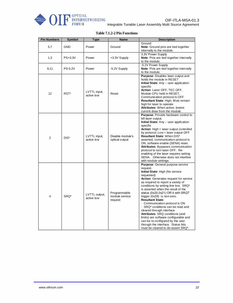
Table 7.1.2-2 Pin Functions
Pin Numbers Symbol Type Name Description
5,7 GND Power Ground Ground Note: Ground pins are tied together
internally to the module.
1,3 PS+3.3V Power +3.3V Supply 3.3V Power Supply Note: Pins are tied together internally
to the module.
9,11 PS-5.2V Power -5.2V Supply
-5.2V Power Supply
Note: Pins are tied together internally to the module.
12 RST* LVTTL input,
active low Reset
Purpose: Disables laser output and
holds the module in RESET Initial State: Any – user application
specific Action: Laser OFF, TEC OFF,
Module CPU held in RESET, Communication protocol is OFF
Resultant State: High, Must remain
high for laser to operate Attributes: When active, lowest
current draw from the module.
2 DIS* LVTTL input, active low
Disable module’s optical output
Purpose: Provide hardware control to
kill laser output. Initial State: Any – user application
specific
Action: High = laser output controlled by protocol; Low = laser output OFF
Resultant State: When DIS* asserted, communication protocol is
ON, software enable (SENA) reset. Attributes: Bypasses communication
protocol to turn laser OFF. Re-enabling of the laser requires setting
SENA. Otherwise does not interfere with module settings.
4 SRQ* LVTTL output,
active low
Programmable module service
request
Purpose: General purpose service
request. Initial State: High (No service
requested) Action: Generates request for service
as required to report a variety of conditions by setting line low. SRQ*
is asserted when the result of the
status (0x20,0x21) OR’d with SRQT trigger (0x28) is non-zero.
Resultant State: · Communication protocol is ON
· SRQ* conditions can be read and cleared through interface
Attributes: SRQ conditions (and limits) are software configurable and
can be re-configured by the user
through the interface. Status bits must be cleared to de-assert SRQ*.
OIF-ITLA-MSA-01.3
Integrable Tunable Laser Assembly Multi Source Agreement
www.oiforum.com 23
Pin Numbers Symbol Type Name Description
6 MS*
LVTTL input,
active low-high transition
Module IO Select
(Reset communications
interface)
Purpose: Provide hardware control to
reset physical interface Initial State: Any – user application
specific
Action: High or LOW = No effect; Low to High transition – Reset
communications interface, clear input buffers, terminate current packet
Resultant State: Communication can be commenced upon deassertion with
a new packet. Attributes: Provides ability to reset
communications interface
8 TxD LVTTL output Module’s Transmit
Data
Purpose: Transmit outbound packets from module
10 RxD LVTTL input Module’s Receive
Data
Purpose: Receive inbound packets
from host
13 OIF Reserved
LVTTL input OIF Reserved
No user connection
Purpose: Provide for possible future expansion of communications
interfaces
14 DitherAA
2.5V p-p
sinusoidal, analog input
Dither amplitude
analog signal
Purpose: Provide trace tone
capability. AC coupled inside ITLA. Pull down to ground if not used.
OIF-ITLA-MSA-01.3
Integrable Tunable Laser Assembly Multi Source Agreement
www.oiforum.com 24
7.1.3 Electrical Characteristics
Table 7.1.3-1: Electrical Characteristics
Parameter Symbol Min Typ Max Unit
+3.3V Supply voltage VCC 3.15 3.30 3.45 V
+3.3V Supply current ICC 1500 mA
(Peak12
)
-5.2V Supply voltage VEE --5.45 -5.20 -4.94 V
-5.2V Supply current IEE -1200 -1000 mA
(Peak13
)
Power Dissipation14
PD 6.6 W
Input voltage, low VIL 0.0 0.8 V
Input voltage, high VIH 2.0 3.45 V
Output voltage, low
(IOL= 4 mA) VOL 0.0 0.6 V
Output voltage,
high (IOH= -4 mA) VOH 2.4 Vcc V
Power supply noise (for power supplied to the
module) (100Hz to 20MHz)
1.0 %rms
Analog Amplitude dither
(DitherAA) modulation voltage (peak to peak).
0 1.25 2.5 Vpp
Analog Amplitude dither input
voltage range peak to peak swing. Accuracy is
manufacturer specific.
0 5 10 %pp
Analog Amplitude dither (DitherAA) input impedance
(AC coupled circuitry in ITLA)
10 k
10 pF
Analog amplitude sinusoidal dither -3dB bandwidth
10 1000 kHz
12
The instantaneous current cannot exceed 1.5 amps. 13
The absolute value of the instantaneous current cannot exceed 1.2 amps. 14
The dual supply configuration allows an ITLA to either draw all its power from a single supply or from both supplies as long as the total average power dissipation does not exceed PD.
OIF-ITLA-MSA-01.3
Integrable Tunable Laser Assembly Multi Source Agreement
www.oiforum.com 25
The module must be able to withstand the following conditions without permanent damage.
Table 7.1.3-2: Absolute Maximum Ratings
Parameter Symbol Min Max Unit
Operating ‘base of butterfly’
temperature range15
TBTF -5 +70 C
Total power dissipation 6.6 W
Storage temperature range TSTORE -40 +85 C
Storage relative humidity 16
RH 5 95
%
Operating relative humidity 16
RH 5 85
%
Signal pin voltage -0.5 VCC + 0.3 V
Power Pin Voltage 3.3V supply -0.3 3.6 V
Power Pin Voltage -5.2V supply -5.5 +0.3 V
15
Requires adequate heat sinking 16
Non condensing
OIF-ITLA-MSA-01.3
Integrable Tunable Laser Assembly Multi Source Agreement
www.oiforum.com 26
7.2 Communication Interface
The communications interface transfer the 32-bit packet with the high order byte (byte 1) transmitted first.
Table 7.1.3-1: Communication Byte Numbering
Byte 1 Byte 2 Byte 3 Byte 4
Bits 31:24 Bits 23:16 Bits 15:8 Bits 7:0
7.2.1 RS232 Communications Interface
The RS232 interface uses a 3-wire implementation (Tx, Rx + ground)
17.
The default baud rate (for initial communication) is 9600 baud which remains in effect otherwise changed or reconfigured as a module default. The maximum supported baud rate is 115.2 kbaud. The interface is configured as 8 bit, no parity, 1 stop bit, no echo, no flow control, and is fully capable of transferring binary data. The following figure shows the timing of a RS232 signal transmitting 0xAA. The LSB
18 is transmitted first.
The interface generates LVTTL output signal levels. The interface consists of the pins shown in the following table.
Table 7.2.1-1 RS232 Physical Interface Pins
PIN I/O FUNCTION
RxD input LVTTL serial input (break signal is 0v)
TxD output LVTTL serial output (break signal is 0v)
Gnd ground Ground
MS* input LVTTL Module Select (Used for RS232 Interface reset or tied
low) Does not deselect the interface.
Figure 7.2-1 shows the interface timing. The MS* line is used to synchronize packet framing of the RS232 interface. It can be used to reset the serial interface and clear the I/O buffers on a low to high transition. By default, a low to high transition on MS* can be configured to reset the interface baud rate to the default. This behavior can be configured through the IOCAP register.
17
This physical interface may be better described as an ASYNC interface but is usually referred to by the industry as an RS232 implementation. 18
Least significant bit
Start
Stop 0
1
2
3
4
5
6
7
OIF-ITLA-MSA-01.3
Integrable Tunable Laser Assembly Multi Source Agreement
www.oiforum.com 27
Figure 7.2-1 RS232 Timing
Note that de-asserting the MS* line does not tri-state the Tx line. The following figure (Figure 7.2-2) also shows a case in which a CE or XE (communications error or execution error) is asserted. For the default configuration on the RS232 interface, the SRQ* line is asserted for execution errors from pending operations
19. The conditions for which the
SRQ* line is asserted are configurable. See (SRQ* Trigger register (0x28)).
Figure 7.2-2 RS232 Communication or Execution Error Timing
The IOCap register has the following format and assumes default values upon power up or hardware reset. 15 14 13 12 11 10 9 8 7 6 5 4 3 2 1 0
0x0 RMS 0x0 Reserved
(0x0)
Current Baud Rate Supported Baud Rates
Bits 0-3 – Maximum baud rate supported by the module
20. (Not writable)
19
By default, non-pending operations which result in an execution error do not assert SRQ. 20
The assumption is that the module will support all RS232 baud rates shown in the table to the specified maximum baud rate.
OIF-ITLA-MSA-01.3
Integrable Tunable Laser Assembly Multi Source Agreement
Bit 8 – Reserved (0x0). Bits 9-11 Reserved Bits 12 – RMS - Configurable action upon low to high transition of MS*
0x0 – Baud rate will be reset to default (0x00) and input buffer cleared upon low to high transition of MS* (default). 0x1 – Clear the input buffers but do not reset the baud rate.
Bits 14-15 – Reserved (default 0x00)
OIF-ITLA-MSA-01.3
Integrable Tunable Laser Assembly Multi Source Agreement
www.oiforum.com 29
8 Transport Layer
8.1 Overview The transport layer encapsulates the command and response packets to form a 32-bit frame. Figure 8.1-1 and Figure 8.1-2 depict the in-bound and out-bound frames. The transport layer is responsible for the fields in white. The application layer is responsible for the shaded fields below. Note that the high order bit (left most bit) is numbered 31.
Figure 8.1-1 In-Bound (Host to Module) Frame
31 30 29 28 27 Bits 26:0
Checksum LstRsp Command packet being framed
Figure 8.1-2 Out-Bound (Module to Host) Frame
31 30 29 28 27 26 Bits 25:0
Checksum CE 1 Response packet being framed
Figure 8.1-3 Transport Layer Field Definitions
Field In-Bound
(Host to Module) Out-Bound
(Module to Host)
Application Layer
Packet to be Framed
27 bits Bits 26:0
26 bits Bits 25:0
Checksum
Bits 31:28
BIP-4 checksum computed over a 32 bit word with the leading 4 bits
pre-pended to the 28 bit packet and set to zero.
BIP-4 checksum computed over a 32 bit word with the
bits 31:28 set to zero and bits 27:26 defined by the
transport layer prior to the BIP-4 computation.
LstRsp/CE
Bit 27 (Communication
Error)
Bit set to logic 0 when the checksum
is consistent. Bit set to logic 1 forces module to
resend last valid packet. Used when the checksum is inconsistent.
Bit set to logic 0 when the checksum is consistent. Bit set to logic 1 when the checksum is inconsistent.
Each in-bound and out-bound packet contains a 4 bit checksum. The checksum is computed over all the bits being encapsulated using a BIP-4 checksum.
8.2 Checksum The checksum is a BIP-4
21 checksum is computed by xor’ing all the bytes in the packet
together and then xor’ing the left nibble of the result with the right nibble of the result. The checksum provides a basic level of consistency check for the communications transfer.
printf("Packet prior to checksum %2.2x %2.2x %2.2x %2.2x\n", data[0],
data[1],data[2],data[3]);
data[0]|= (bip4<<4); /* Add in the BIP-4 checksum */
printf("Bip-4 checksum value is %x\n",bip4);
printf("Packet with checksum %2.2x %2.2x %2.2x %2.2x\n", data[0],
data[1],data[2],data[3]);
}
OIF-ITLA-MSA-01.3
Integrable Tunable Laser Assembly Multi Source Agreement
www.oiforum.com 31
9 Command Interface (Application Layer)
9.1 Command Format
9.1.1 In-Bound (Host to Module)
The command packets consist of a 4 byte packet of which the lower 28 bits are used. The 4 high order bits are redefined by the transport layer (where the packet checksum is added). The shaded area shows the bits to be replaced by the transport layer.
Inbound Byte 0
31 30 29 28 27 26 25 24
0x0 (To be defined by transport layer) 0x0 RW
(R=0, W=1)
Inbound Byte 1
23 22 21 20 19 18 17 16
Register Number (0x00 – 0xff)
Inbound Byte 2
15 14 13 12 11 10 9 8
Data 15:8
Inbound Byte 3
7 6 5 4 3 2 1 0
Data 7:0
9.1.2 Out-Bound (Module to Host)
The response packet consists of a 4 byte packet of which the lower 26 bits are used. The 6 high order bits contain a checksum and two flags which are redefined by the transport layer. The shaded area shows the bits to be replaced by the transport layer.
Outbound Byte 0
31 30 29 28 27 26 25 24
0x0 (To be defined by transport layer) Status
Outbound Byte 1
23 22 21 20 19 18 17 16
Register Number (0x00 – 0xff)
Outbound Byte 2
15 14 13 12 11 10 9 8
Data 15:8
Outbound Byte 3
7 6 5 4 3 2 1 0
Data 7:0
The status field (bits 25:24) take on one of the 4 values in Table 9.1.2-1.
Table 9.1.2-1: Packet Status Flags
Bits 1:0 Value Status Field
0x00 OK flag, Normal return status
0x01 XE flag, (execution error)
0x02 AEA flag, (Automatic extended addressing result being returned or ready to write)
0x03 CP flag, Command not complete, pending
OIF-ITLA-MSA-01.3
Integrable Tunable Laser Assembly Multi Source Agreement
www.oiforum.com 32
Bits 25:24=0x00, OK flag, Normal. No execution errors and not using AEA mode for returning result. Bits 25:24=0x01, XE flag (Execution Error) signifies that the previous command failed to execute properly. (Bits 1:0) not equal 0x01 signifies that the previous command completed successfully or is pending.
Bits 25:24=0x02, AEA flag, (automatic extended addressing) mode, indicates that the register (for which a read or write operation has been given) requires a multi-byte sequence
22. The unsigned value is returned in bytes 2 and 3 and represents the number
of bytes in the multi-byte response. Bits 25:24=0x03, CP flag, Command pending (command not complete), indicates that the command will take longer than the maximum timeout specified for this device type.
23 In
this case the module returns a response within the timeout period and continues to execute the requested operation. The host can poll the module’s status register (0x00) through the communication’s interface to determine if the operation has completed.
If the CP flag is set, the out-bound byte 3 will be 0x00 and out-bound byte 2 will have one of eight bits set (bits 15:8) showing which bit the pending operation has been assigned. Note that this bit mapping is identical to the bits 15:8 in the response of the NOP (x000) command. Note that a write to an AEA register is always an AEA operation and may also be a pending operation. In this case, the module returns the AEA flag (0x02) in the status field and assigns a pending operation ID in the “Data 15:8” in the of the outbound response packet.
22
In the case where a write was done to a register that supports AEA, outbound bytes 2 and 3 are ignored. The write command will need to be repeated this time addressing the AEA-EAR register instead. 23
Device types/classes are specific implementations of tunable devices.
OIF-ITLA-MSA-01.3
Integrable Tunable Laser Assembly Multi Source Agreement
www.oiforum.com 33
9.2 Register Summary
Table 9.2-1: Table of Registers (Commands)
Command Register
Name
Read /
Write AEA
Non-
volatile (NV)
Description
General Module Commands
0x00 NOP R/W
Provide a way to read a pending response as
from an interrupt, to determine if there is pending operation, and/or determine the specific error
condition for a failed command.
0x01 DevTyp R AEA Returns device type (tunable laser source, filter,
modulator, etc) as a null terminated string.
0x02 MFGR R AEA Returns manufacturer as a null terminated string in AEA mode (vendor specific format)
0x03 Model R AEA Returns a model null terminated string in AEA mode (vendor specific format)
0x04 SerNo R AEA Returns the serial number as null terminated string in AEA mode
0x05 MFGDate R AEA Returns the mfg date as a null terminated string.
0x06 Release R AEA Returns a manufacturer specific firmware release as a null terminated string in AEA mode
0x07 RelBack R AEA Returns manufacturer specific firmware backwards compatibility as a null terminated
string
0x08 GenCfg RW General module configuration
0x09 AEA-EAC R Automatic extended address configuration
register
0x0A AEA-EA R Automatic extended address (16 bits)
0x0B AEA-EAR RW Location accessed “thru” AEA-EA and AEA-EAC
0x0C Reserved
0x0D IOCap RW NV Physical interface specific information (such as
data rate, etc.)
0x0E EAC RW Extended address configuration register - auto incr/decr flag on read and on write and
additional address bits
0x0F EA RW Extended address (16 bits)
0x10 EAR RW Location accessed “thru” EA and EAC
0x1324
LstResp R Returns last response
0x14 DLConfig RW Download configuration register
0x15 DLStatus R Download status register
0x17 – 0x1F
Reserved -- --
24
This command is deprecated. It may be available in some ITLA implementations.
OIF-ITLA-MSA-01.3
Integrable Tunable Laser Assembly Multi Source Agreement
www.oiforum.com 34
Module Status Commands
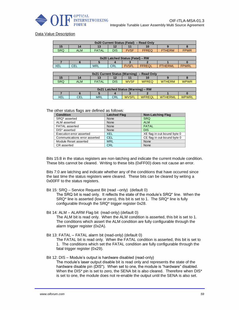
0x20 StatusF RW Contains reset status, optical faults and alarms, and enable status.
0x21 StatusW RW Contains reset status, warning optical faults and alarms, and enable status.
0x22 FPowTh RW NV Returns/Sets the threshold for the output power
FATAL condition encoded as dB*100
0x23 WPowTh RW NV Returns/Sets the threshold for the power warning
encoded as dB*100
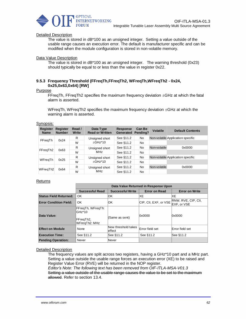
0x24 FFreqTh RW NV
Returns/Sets the threshold for the frequency
FATAL condition encoded as GHz*10. Also see
the optional MHz resolution FFreqTh2 register 0x63
0x25 WFreqTh RW NV
Returns/Sets the threshold for the frequency
error warning encoded as GHZ*10. Also see the
optional MHz resolution WFreqTh2 register 0x64.
0x26 FThermTh RW NV Returns/Sets the threshold for thermal deviations
(> C*100) at which FATAL is asserted.
0x27 WThermTh RW NV Returns/Sets the threshold for thermal deviations
(> C*100) at which a warning is asserted.
0x28 SRQT RW NV Indicates which bits in the Fatal & Warning status registers, 0x20-0x21, cause a SRQ condition and
asserts the SRQ* line.
0x29 FatalT RW NV Indicates which bits in the Fatal & Warning status register, 0x20-0x21, assert a FATAL condition
0x2A ALMT RW NV
Indicates which bits in the status registers, 0x20, 0x21, cause an alarm condition. (Default
behavior asserted whether laser is LOCKED on frequency.
0x2B –
0x2F Reserved
Module Optical Commands
0x30 Channel RW NV
Setting valid channel causes a tuning operation
to occur. Also see the optional MHz resolution ChannelH register 0x65.
0x31 PWR RW NV Sets the optical power set point as encoded as
dBm*100
0x32 ResEna RW Reset/Enable - Enable output, hard and soft
reset
0x33 MCB RW NV Various module configurations
0x34 GRID RW NV
Allows the grid spacing to be set for channel
numbering. Also see the optional MHz resolution GRID2 register 0x66.
0x35 FCF1 RW NV Allows the first channel’s frequency to be defined for channel numbering. (THz) Also see the
optional MHz resolution FCF3 register 0x67.
0x36 FCF2 RW NV Allows the first channel’s frequency to be defined for channel numbering. (GHz*10) Also see the
optional MHz resolution FCF3 register 0x67.
0x37 –
0x3F Reserved Reserved for OIF configuration registers
0x40 LF1 R Returns channel’s frequency as THz. Also see the optional MHz resolution LF3 register 0x68.
0x41 LF2 R Returns channel’s frequency as GHZ*10. Also see the optional MHz resolution LF3 register
0x68.
0x42 OOP R Returns the optical power encoded as dBm*100
0x43 CTemp R Returns the current temperature (monitored by
the temperature alarm) encoded as C*100.
0x44 – 0x4E
Reserved Reserved for OIF status registers
OIF-ITLA-MSA-01.3
Integrable Tunable Laser Assembly Multi Source Agreement
www.oiforum.com 35
Module Capabilities
0x4F FTFR R Returns min/max fine tune frequency range (MHz)
0x50 OPSL R Returns the min possible optical power setting
0x51 OPSH R Returns the max possible optical power setting
0x52 LFL1 R Laser’s first frequency (THz). Also see the
optional MHz resolution LFL3 register 0x69
0x53 LFL2 R Laser’s first frequency (GHz*10). Also see the
optional MHz resolution LFL3 register 0x69
0x54 LFH1 R Laser’s last frequency (THz). Also see the optional MHz resolution LFH3 register 0x6A
0x55 LFH2 R Laser’s last frequency (GHz*10). Also see the optional MHz resolution LFH3 register 0x6A
0x56 LGrid R Laser’s minimum supported grid spacing (GHz*10). Also see the optional MHz resolution
LGrid2 register 0x6B
OIF-ITLA-MSA-01.3
Integrable Tunable Laser Assembly Multi Source Agreement
www.oiforum.com 36
MSA Commands 0x57 Currents R AEA Return module specific currents
0x58 Temps R AEA Return module specific temperatures
0x59 DitherE RW NV Digital dither enable
Optional
features
0x5A DitherR RW NV Digital dither rate
0x5B DitherF RW NV Digital dither frequency
modulation
0x5C DitherA RW NV Digital dither amplitude
modulation.
0x5D TBTFL RW NV Sets the lower boundary for a warning on base of the butterfly temperature
0x5E TBTFH RW Sets the upper boundary for a warning on base of the butterfly temperature
0x5F FAgeTh RW NV
Specifies the maximum end of life (EOL) percent
aging at which fatal condition for the vendor specific error is asserted
0x60 WAgeTh RW NV Specifies the maximum end of life (EOL) percent aging at which warning condition for the vendor
specific error is asserted
0x61 Age R Returns the laser’s age as a percentage
0x62 FTF RW Fine tune frequency adjustment of
laser output.
Optional
feature
0x63 FFreqTh2 RW NV
Returns/Sets the MHz part of the
frequency FATAL threshold. Used in conjunction with FFreqTh
(0x24)
Hig
h r
eso
lutio
n r
egis
ters
ad
de
d d
uri
ng
ma
inte
na
nce
. A
pple
s t
o
Pro
toco
l V
ers
ion
3.0
.0
0x64 WFreqTh2 RW NV
Returns/Sets the MHz part of the frequency error warning
threshold. Used in conjunction with WFreqTh (0x25)
0x65 ChannelH RW NV High word of 32 bit channel value, used in conjunction with Channel
(0x30)
0x66 GRID2 RW NV Returns/Sets the MHz part of the channel grid spacing. Used in
conjunction with GRID (0x34)
0x67 FCF3 RW NV
Returns/Sets the MHz part of the
first channel’s frequency. Used in conjunction with FCF1, FCF2
(0x35, 0x36)
0x68 LF3 R
Returns the MHz part of the current channel laser frequency.
Used in conjunction with LF1, LF2 (0x40,0x41)
0x69 LFL3 R
Laser’s first frequency (MHz).
Used in conjunction with LFL1, LFL2 (0x52, 0x53).
0x6A LFH3 R Laser’s last frequency (MHz) ). Used in conjunction with LFH1,
LFH2 (0x54, 0x55).
0x6B LGrid2 R
Laser’s minimum supported grid
spacing (MHz). Used in
conjunction with LGrid (0x56).
0x6C- 0x7F Reserved
Manufacturer Specific
0x80-0xFE Manufacturer Specific
OIF-ITLA-MSA-01.3
Integrable Tunable Laser Assembly Multi Source Agreement
www.oiforum.com 37
9.3 Command Description Format The commands are described using 5 sections (note the shaded boxes in the table represent fields that are not applicable):
1) Purpose – Describes the basic
purpose of the command. 2) Synopsis – Tabular format
summarizing the command behavior and arguments
3) Returns – Tabular format
summarizing the possible returns for successful and error conditions.
Status field (register 0x00)
Error condition field (0x00)
Data value (16 bit)
Effect on module
Execution time
Pending operation 4) Detailed Description – Describes the detailed behavior of the command 5) Data Value Description – Describes the data value for the command.
The Synopsis section describes the following:
Every command will show two lines; one for read and one for write. In the case of a read, the data value type is shown for the response packet. For a write, the data value type is shown as the operand of the command. (Note the shaded boxes in the table represent fields that are not applicable):
1) The “Response Generated” column indicates the maximum interval of time from
when the command is acknowledged by the module until the module will generate a response. The transmission time of the response is dependent on the physical interface data rate and characteristics. See §7.2-Communication Interface.
2) The “Can Be Pending” column indicates if the command is allowed not to finish in
the “Response Generated” time interval. 3) The “Volatile” column, if contains non-volatile, indicates that the default value loaded
during power up or hard reset is loaded from non-volatile memory25
. The defaults
25
The default configuration is typically user application specific and once configured is expected to be infrequently modified.
OIF-ITLA-MSA-01.3
Integrable Tunable Laser Assembly Multi Source Agreement
www.oiforum.com 38
may be configured and stored using the GenCfg:SDC operation. See §9.4.9-General Module Configuration (GenCfg 0x08) [RW].
4) Where relevant, the “Default Contents” column indicates what the default contents
would be for a freshly booted or reset module. Note that registers marked non-volatile have defaults values set by the GenCfg:SDC operation.
The Returns section describes the following for successful and failed read and write
operations.
1) Status Field Returned: The value in the status field (bits 25:24) in the out-bound
response (module to host). 2) Error Condition Field: The possible values contained in the NOP (0x00) commands
error field because of the command’s execution or failure to execute. 3) Data Value: A description of the data value contained in the modules response. 4) Effect on Module: Indicates the resultant state of the module after requested
operation has terminated. 5) Execution Time:The maximum time for the command to complete execution. Note
this is different than the generation of a response described in the previous table. 6) Pending Operation: Indicates whether a successful command can return before the
command has completed execution.
OIF-ITLA-MSA-01.3
Integrable Tunable Laser Assembly Multi Source Agreement
www.oiforum.com 39
9.4 Generic Module Commands
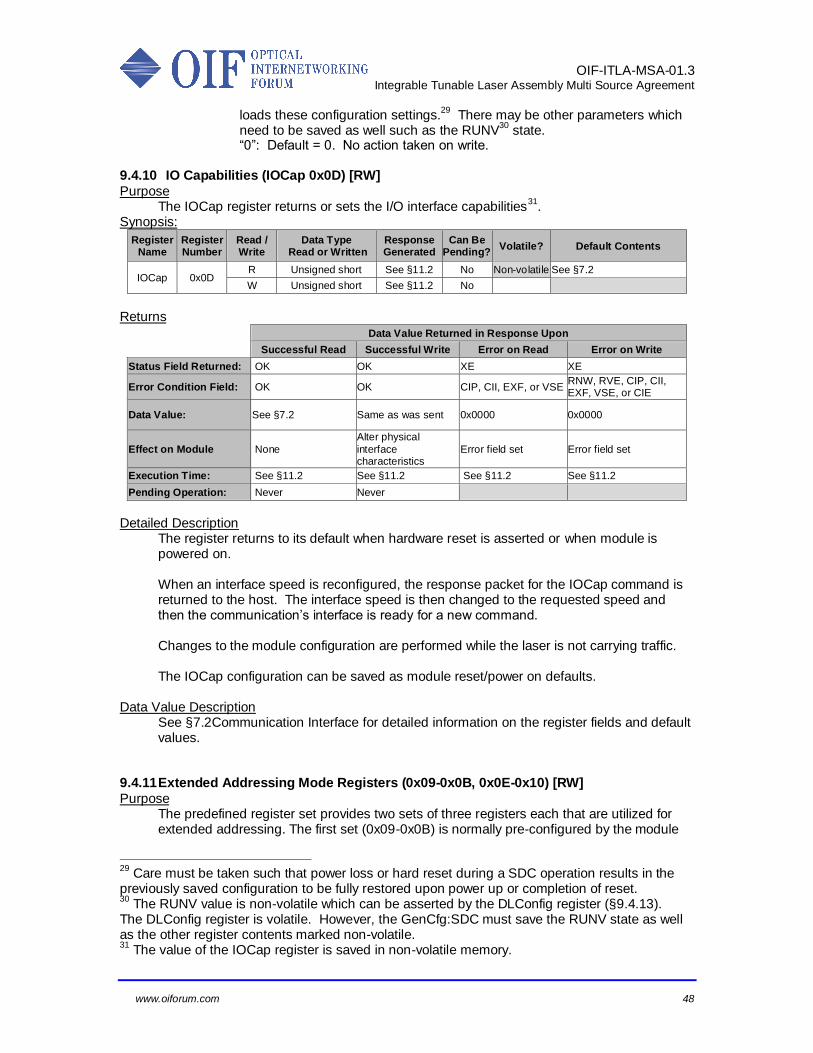
9.4.1 NOP/Status (NOP 0x00) [RW]
Purpose The NOP register provides a way to access the module’s status, returning pending operation status, and the current value of the error field. This register may be read upon receiving an execution error for an immediately preceding command. It can also be polled to determine the status of pending operations.
Synopsis:
Register
Name
Register
Number
Read /
Write
Data Type
Read or Written
Response
Generated
Can Be
Pending? Volatile? Default Contents
NOP 0x00 R Unsigned short See §11.2 No
Bits15:8: 0x00 (pending
bits) Bit 7:5: 0x0 (reserved)
Bit 4: MRDY (0x0) Bits 3:0: 0x0 (error field)
W Unsigned short See §11.2 No
Returns
Data Value Returned in Response Upon
Successful Read Successful Write Error on Read Error on Write
Status Field Returned: OK OK XE XE
Error Condition Field: OK OK EXF, or VSE EXF, or VSE
Data Value:
Pending command status (bits 15:8), Bit
4, and error condition field (bits 3:0)
Same as was sent 0x0000 0x0000
Effect on Module None, by definition None, by definition Error field set Error field set
Execution Time: See §11.2 See §11.2 See §11.2 See §11.2
Pending Operation: Never Never
Detailed Description
A write to the NOP register is allowed but the contents are not loaded with the data value from the write command. The NOP command is guaranteed to succeed at all times except possibly during catastrophic failure of the module.
Data Value Description
15 14 13 12 11 10 9 8 7 6 5 4 3 2 1 0
Pending Operation Status 0x0 MRDY Error Field
Bits 15:8 – Pending Operation Flags
A series of eight flag bits indicating which operations, if any, are still pending. Each operation that becomes pending is assigned one of these four bit positions. The module can be periodically polled (by reading the NOP register) to determine which operations have completed. A value of 0x0 indicates that there are no currently pending operations.
Bit 7:5– Always 0x00 (Reserved) Bit 4 – MRDY - Module Ready
26
When “1” indicates that the module is ready for its output to be enabled When “0” indicates that the module is not ready for its output to be enabled.
Bits 3:0 – Error field – Error condition for last completed command
26
De-asserted during module warm up time (see §11.3-Module Warm Up Time) or if an invalid configuration detected. Asserted when module is ready to enable output and carry traffic.
OIF-ITLA-MSA-01.3
Integrable Tunable Laser Assembly Multi Source Agreement
www.oiforum.com 40
A read of the NOP register will return the error condition from the last completed command before setting it to 0x00 to reflect the status of the current command (which is reading the NOP register).
Value
(Bits 3:0) Symbol Meaning
0x00 OK Ok, no errors
0x01 RNI The addressed register is not implemented
0x02 RNW Register not write-able; register cannot be written (read only)
0x03 RVE Register value range error; writing register contents causes value range
error; contents unchanged
0x04 CIP Command ignored due to pending operation
0x05 CII Command ignored while module is initializing, warming up, or contains an
invalid configuration.
0x06 ERE Extended address range error (address invalid)
0x07 ERO Extended address is read only
0x08 EXF Execution general failure
0x09 CIE Command ignored while module’s optical output is enabled (carrying traffic)
0x0A IVC Invalid configuration, command ignored
0x0B-0x0E -- Reserved for future expansion
0x0F VSE Vendor specific error (see vendor specific documentation for more
information)
The device type register is provided such that a host can distinguish between different types of tunable devices.
9.4.2 Device Type (DevTyp 0x01) [R]
Purpose: DevTyp returns the module’s device type. For all tunable lasers covered by this MSA, the module will return the null terminated string “CW ITLA\0” (eight bytes including the terminating null character) indirectly through the AEA mechanism. The device type register is provided such that a host can distinguish between different types of tunable devices.
Synopsis:
Register Name
Register Number
Read / Write
Data Type Read or Written
Response Generated
Can Be Pending?
Volatile? Default Contents
DevTyp 0x01 R AEA (string) See §11.2 No
0x0008 “CW ITLA\0”
W
Returns
Data Value Returned in Response Upon
Successful Read Successful Write Error on Read Error on Write
Status Field Returned: OK XE
Error Condition Field: OK CIP, CII, EXF, or VSE
Data Value: 0x0008
“CW ITLA\0” 0x0000
Effect on Module AEA registers configured to
reference string
Error field set
Execution Time: See §11.2 See §11.2
Pending Operation: Never
Detailed Description
A write to the DevTyp register results in an execution error.
OIF-ITLA-MSA-01.3
Integrable Tunable Laser Assembly Multi Source Agreement
www.oiforum.com 41
Data Value Description DevTyp returns the length of ASCII string. Note that in this case, the null terminated string “CW ITLA\0” contains eight bytes including the null terminating byte.
Example Usage
#
Command (Host to Module) Response (Module to Host)
MFGR returns the module’s manufacturers ID null terminated string indirectly through the AEA mechanism.
Synopsis:
Register
Name
Register
Number
Read /
Write
Data Type
Read or Written
Response
Generated
Can Be
Pending? Volatile? Default Contents
MFGR 0x02 R AEA (string) See §9.5.7 No
0x00xx Manufacturer
W
Returns
Data Value Returned in Response Upon
Successful Read Successful Write Error on Read Error on Write
Status Field Returned: OK XE
Error Condition Field: OK CIP, CII, EXF, or VSE
Data Value: 0x00xx
Manufacturer 0x0000
Effect on Module
AEA registers
configured to reference string
Error field set
Execution Time: See §9.5.7 See §9.5.7
Pending Operation: Never
Detailed Description
A write to the MFGR register results in an execution error.
Data Value Description MFGR returns the length of a null terminated printable ASCII string. (Maximum 80 bytes)
9.4.4 Model (Model 0x03) [R]
Purpose: Model returns the module’s model designation string indirectly through the AEA mechanism. The null terminated string containing the module’s model designation is
OIF-ITLA-MSA-01.3
Integrable Tunable Laser Assembly Multi Source Agreement
www.oiforum.com 42
placed into a field of not more than 80 bytes in size. The model string is defined by the manufacturer
Synopsis:
Register
Name
Register
Number
Read /
Write
Data Type
Read or Written
Response
Generated
Can Be
Pending? Volatile? Default Contents
Model 0x03 R AEA (string) See §9.5.7 No
0x00xx
Model
W
Returns
Data Value Returned in Response Upon
Successful Read Successful Write Error on Read Error on Write
Status Field Returned: OK XE
Error Condition Field: OK CIP, CII, EXF, or VSE
Data Value: 0x00xx Model
0x0000
Effect on Module
AEA registers
configured to reference string
Error field set
Execution Time: See §11.2 See §11.2
Pending Operation: Never
Detailed Description
A write to the Model register results in an execution error.
Data Value Description Model returns the length of a null terminated printable ASCII string. (Maximum 80 bytes)
9.4.5 Serial Number (SerNo 0x04) [R]
Purpose: SerNo returns the module’s serial number string indirectly through the AEA mechanism. The null terminated string containing the module’s serial number is placed into a field of not more than 80 bytes in size. The serial number string is defined by the manufacturer.
Synopsis:
Register Name
Register Number
Read / Write
Data Type Read or Written
Response Generated
Can Be Pending?
Volatile? Default Contents
SerNo 0x04 R AEA (string) See §9.5.7 No
0x00xx SerNo
W
Returns
Data Value Returned in Response Upon
Successful Read Successful Write Error on Read Error on Write
Status Field Returned: OK XE
Error Condition Field: OK CIP, CII, EXF, or VSE
Data Value: 0x00xx
SerNo string 0x0000
Effect on Module AEA registers configured to
reference string
Error field set
Execution Time: See §11.2 See §11.2
Pending Operation: Never
Detailed Description
A write to the SerNo register results in an execution error.
OIF-ITLA-MSA-01.3
Integrable Tunable Laser Assembly Multi Source Agreement
www.oiforum.com 43
Data Value Description
SerNo returns the length of a null terminated printable ASCII string. (Maximum 80 bytes) .
9.4.6 Manufacturing Date (MFGDate0x05) [R]
Purpose: MFGDate returns the manufacturing date string of the module indirectly through the AEA mechanism. The null terminated string containing the date string is contained in a field size of 12 bytes.
Synopsis:
Register Name
Register Number
Read / Write
Data Type Read or Written
Response Generated
Can Be Pending?
Volatile? Default Contents
MFGDate 0x05 R AEA (string) See §11.2 No
0x000C Date
W
Returns
Data Value Returned in Response Upon
Successful Read Successful Write Error on Read Error on Write
Status Field Returned: OK XE
Error Condition Field: OK CIP, CII, EXF, or VSE
Data Value:
0x000C
Date
“DD-MON-YYYY\0”
0x0000
Effect on Module AEA registers configured to
reference string
Error field set
Execution Time: See §11.2 See §11.2
Pending Operation: Never
Detailed Description
A write to the MFGDate register results in an execution error.
Data Value Description The MFGDate register returns the date of manufacture as a null terminated ASCII string (12 characters) formatted as “DD-MON-YYYY”. DD is a 2 character field with leading zeros indicating the day of the month, MON is 3 character representation of the month (JAN,FEB,MAR,APR,MAY,JUN,JUL,AUG,SEP,OCT,NOV,DEC), and YYYY is the 4 digit year. Example: “04-APR-2001”
OIF-ITLA-MSA-01.3
Integrable Tunable Laser Assembly Multi Source Agreement
www.oiforum.com 44
9.4.7 Release (Release 0x06) [R]
Purpose: Release returns the release string of the module indirectly through the AEA mechanism. The null terminated string containing the module release information is placed into a field of not more than 80 bytes in size. Note that a module may have one or more firmware and/or hardware revisions to track. The release field also encodes the application space identifier.
Synopsis:
Register Name
Register Number
Read / Write
Data Type Read or Written
Response Generated
Can Be Pending?
Volatile?
Default Contents
Release 0x06 R AEA (string) See §11.2 No
0x00xx
Module release
W
Returns
Data Value Returned in Response Upon
Successful Read Successful Write Error on Read Error on Write
Status Field Returned: OK XE
Error Condition Field: OK CIP, CII, EXF, or VSE
Data Value: 0x00xx
Module release 0x0000
Effect on Module AEA registers configured to
reference string
Error field set
Execution Time: See §11.2 See §11.2
Pending Operation: Never
Detailed Description
A write to the Release register results in an execution error. The module release string must contain at least protocol version and either a firmware or a hardware version.
OIF-ITLA-MSA-01.3
Integrable Tunable Laser Assembly Multi Source Agreement
www.oiforum.com 45
Data Value Description Release returns the length of a null terminated printable ASCII string. (Maximum 80 bytes)
The release string consists of one or more concatenated release fields with a “:’ used as the delimiter. A release field is white space delimited and consists of an identifier followed by a release version consisting of 3 base 10 numeric fields formatted as X.Y.Z. The application space identifier are defined in §11.1 - Optical Characteristics. Format: “<Identifier1> <space> <X1.Y1.Z1> : <Identifier2> <space> <X2.Y2.Z2> …”
Identifier Description Field Values Description
PV Protocol version27
X 0:255 Major release - Change in fit, form, or function
HW Hardware release Y 0:255 Minor release - Improvements but no change in fit, form, or function
FW Firmware release Z 0:255 Patch Level
AS Application Space
<others> Manufacturer specific
The release fields are guaranteed to follow the following relationship.
XNEW > XOLD YNEW > YOLD ZNEW and ZOLD are not necessarily sequential and shall not be compared.
Example: For example a module showing a firmware revision and a hardware revision would return a string like: “PV:2.0.0:FW 1.0.1:HW 3.2.1:AS A1”.
27
The protocol version references the protocol document (this document) and indicates which version the module conforms.
OIF-ITLA-MSA-01.3
Integrable Tunable Laser Assembly Multi Source Agreement
Purpose: RelBack returns the release backwards compatibility string of the module indirectly through the AEA mechanism. The null terminated string containing the earliest release string which is fully backwards compatible with the current module. The string is contained in a field of not more than 80 bytes in size. Note that a module may have one or more firmware and/or hardware revisions to track as described in the Release (0x06) register.
Synopsis:
Register Name
Register Number
Read / Write
Data Type Read or Written
Response Generated
Can Be Pending?
Volatile? Default Contents
RelBack 0x07 R AEA (string) See §11.2 No
0x00xx Release
W
Returns
Data Value Returned in Response Upon
Successful Read Successful Write Error on Read Error on Write
Status Field Returned: OK XE
Error Condition Field: OK CIP, CII, EXF, or VSE
Data Value: 0x00xx
Release 0x0000
Effect on Module AEA registers configured to
reference string
Error field set
Execution Time: See §11.2 See §11.2
Pending Operation: Never
Detailed Description
A write to the RelBack register results in an execution error. Data Value Description
RelBack returns the length of a null terminated printable ASCII string. (Maximum 80 bytes) The release string consists of one or more concatenated release fields with a “:’ used as the delimiter. A release field is white space delimited and consists of an identifier followed by a release version consisting of 3 base 10 numeric fields formatted as X.Y.Z. Format: “<Identifier1> <space> <X1.Y1.Z1> : <Identifier2> <space> <X2.Y2.Z2> …”
Identifier Description Field Values Description
HW Hardware release X 0:255 Major release - Change in fit, form, or function
FW Firmware release Y 0:255 Minor release - Improvements but no change in fit, form,
or function
<others> Manufacturer specific Z 0:255 Patch Level – Not part of a normal release scheme
The release fields are guaranteed to follow the following relationship.
XNEW > XOLD YNEW > YOLD ZNEW and ZOLD are not necessarily sequential and shall not be compared to
determine whether ZNEW or ZOLD is newer.
OIF-ITLA-MSA-01.3
Integrable Tunable Laser Assembly Multi Source Agreement
www.oiforum.com 47
Example: For example a module showing a firmware revision and a hardware revision might return a string: “PV:1.0.1:FW 1.0.1:HW 3.2.1” and might return a RelBack string: “PV:1.0.1:FW 1.0.0:HW 3.2.1”. This indicates that the current FW is backwards compatible with drivers written for FW 1.0.0 and that the hardware and protocol versions are the same.
9.4.9 General Module Configuration (GenCfg 0x08) [RW]
Purpose GenCfg defines the general module configuration for the generic tunable device. For the tunable laser, the register is used to save the power on/reset module configuration defaults.
Synopsis:
Register Name
Register Number
Read / Write
Data Type Read or Written
Response Generated
Can Be Pending?
Volatile? Default Contents
GenCfg 0x08 R Unsigned short See §11.2 No 0x0000
W Unsigned short See §11.2 Yes
Returns
Data Value Returned in Response Upon
Successful Read Successful Write Error on Read Error on Write
Status Field Returned: OK OK XE XE
Error Condition Field: OK OK CIP, CII, EXF, or VSE RNW, RVE, CIP, CII,
EXF, CIE, or VSE
Data Value: 0x0000 Same as sent or
pending ID 0x0000 0x0000
Effect on Module None
Store registers marked non-volatile
in non-volatile memory
Error field set Error field set
Execution Time: See §11.2 See §11.2 See §11.2 See §11.2
Pending Operation: Never Yes
Detailed Description
Reading GenCfg always returns 0x0. Writing to GenCfg is only allowed when laser is not carrying traffic (optical output disabled)
28.
The self clearing SDC (Store Default Configuration) flag is used to initiate a transfer of all registers marked non-volatile to non-volatile memory. The values are restored on power up or module reset.
“1”: Save all non-volatile module configuration values in non-volatile memory. This bit is self clearing. Upon power on or hard reset, the module
28
Some module configuration changes may cause a traffic interrupting event. Therefore, configuration changes (writes to GenCfg) are only allowed when the optical output is disabled.
OIF-ITLA-MSA-01.3
Integrable Tunable Laser Assembly Multi Source Agreement
www.oiforum.com 48
loads these configuration settings.29
There may be other parameters which need to be saved as well such as the RUNV
30 state.
“0”: Default = 0. No action taken on write. 9.4.10 IO Capabilities (IOCap 0x0D) [RW]
Purpose The IOCap register returns or sets the I/O interface capabilities
31.
Synopsis:
Register Name
Register Number
Read / Write
Data Type Read or Written
Response Generated
Can Be Pending?
Volatile? Default Contents
IOCap 0x0D R Unsigned short See §11.2 No Non-volatile See §7.2
W Unsigned short See §11.2 No
Returns
Data Value Returned in Response Upon
Successful Read Successful Write Error on Read Error on Write
Status Field Returned: OK OK XE XE
Error Condition Field: OK OK CIP, CII, EXF, or VSE RNW, RVE, CIP, CII, EXF, VSE, or CIE
Data Value: See §7.2 Same as was sent 0x0000 0x0000
Effect on Module None
Alter physical
interface characteristics
Error field set Error field set
Execution Time: See §11.2 See §11.2 See §11.2 See §11.2
Pending Operation: Never Never
Detailed Description
The register returns to its default when hardware reset is asserted or when module is powered on. When an interface speed is reconfigured, the response packet for the IOCap command is returned to the host. The interface speed is then changed to the requested speed and then the communication’s interface is ready for a new command. Changes to the module configuration are performed while the laser is not carrying traffic. The IOCap configuration can be saved as module reset/power on defaults.
Data Value Description See §7.2Communication Interface for detailed information on the register fields and default values.
Purpose The predefined register set provides two sets of three registers each that are utilized for extended addressing. The first set (0x09-0x0B) is normally pre-configured by the module
29
Care must be taken such that power loss or hard reset during a SDC operation results in the previously saved configuration to be fully restored upon power up or completion of reset. 30
The RUNV value is non-volatile which can be asserted by the DLConfig register (§9.4.13). The DLConfig register is volatile. However, the GenCfg:SDC must save the RUNV state as well as the other register contents marked non-volatile. 31
The value of the IOCap register is saved in non-volatile memory.
OIF-ITLA-MSA-01.3
Integrable Tunable Laser Assembly Multi Source Agreement
www.oiforum.com 49
when the host reads from or writes to a register that supports AEA (automatic extended addressing) mode. The second set is normally pre-configured for large transfers such as a firmware upload or download. Note that two sets of extended address registers is desirable in case an AEA register needs to be accessed during a lengthy upload or download.
Synopsis:
Register Name
Register Number
Read / Write
Data Type Read or Written
Response Generated
Can Be Pending?
Volatile? Default Contents
AEA-EAC 0x09 R Unsigned short See §11.2 No 0x0000
W Unsigned short See §11.2 Yes
AEA-EA 0x0A R Unsigned short See §11.2 No 0x0000
W
AEA-EAR 0x0B R Defined by target
field format See §11.2 No No Default Required
W See §11.2 Yes --
EAC 0x0E R Unsigned short See §11.2 No 0x0000
W Unsigned short See §11.2 Yes
EA 0x0F R Unsigned short See §11.2 No 0x0000
W Unsigned short See §11.2 No
EAR 0x10 R Defined by target
field format See §11.2 No No Default Required
W See §11.2 Yes --
Returns
Data Value Returned in Response Upon
Successful Read Successful Write Error on Read Error on Write
Status Field Returned: OK OK XE XE
Error Condition Field: OK OK CIP, CII, ERE, EXF, or VSE
RNW, RVE, CIP, CII, ERE, ERO, EXF, or VSE
Data Value: See definitions below See definitions below 0x0000 0x0000
Effect on Module
EAC, EA- None EAC, EA- Configured Error field set
Address unchanged
Error field set
Address unchanged EAR- EAC:EA incremented
EAR- Field written, EAC:EA incremented
Execution Time: See §11.2 See §11.2 See §11.2 See §11.2
Pending Operation: Never Yes32
Detailed Description
In order to access a location through the extended addressing interface, the EAC and EA registers must properly configured. This configuration occurs automatically when AEA designated registers are accessed or when the DLConfig process is initiated. Read or write access of a register that supports AEA returns the number of bytes in the field. The access also configures the AEA-EAC and AEA-EA registers. Subsequent reads or writes on AEA-EAR transfers data sequentially from the physical or virtual memory location where the field is stored and may result in a pending operation. Note that although a write to a register that supports AEA access returns the maximum number of bytes to be written, but no data is actually written. The write command must be re-issued to the AEA-EAR register in order to complete the write.
32
Note that writes to the AEA-EAR register or the EAR register may result a pending operation (CP flag) if a non-volatile memory “store” cycle takes longer than the 5ms execution time.
OIF-ITLA-MSA-01.3
Integrable Tunable Laser Assembly Multi Source Agreement
www.oiforum.com 50
Operation on
Register Which
Support AEA
Data Value Sent Status Flags
Effect on AEA Data Value Returned
Read 0x0000 0x02 (AEA)
Configured
Number of bytes
in the previously stored value.
Write
0x0000 0x00 NOT Configured
Maximum number
of bytes that can be stored in the
field.
Number of bytes to be stored in the coming
AEA transfer.
0x02
(AEA) Configured
0xPP00
(Pending ID)
Reading or writing beyond the field boundaries will generate an execution error.
Operation on EAR
Data Value Sent Effect on AEA Data Value Returned
Read 0x0000 0x00 Address incremented after
read
If successful, the
data byte(s). If XE, result undefined.
Write Data byte(s) to be written 0x00 or
0x03 (CP)
Address incremented after
write
0x0000 or
0xPP00 (if pending)
An execution error on read or write does not increment the extended address register’s contents. A soft reset (ResEna 0x32) will abort extended address transfers (firmware uploads or AEA transfers). A low to high transition of MS* will not abort extended address transfers but just clears the input buffers and may reset the baud rate.
Data Value Description See the following sections.
9.4.11.1 Extended Address Configuration (EAC 0x09 & 0x0E) The first register, AEA-EAC (0x09) or EAC (0x0E), configures the extended addressing mode.
15 14 13 12 11 10 09 08 07 06 05 04 03 02 01 00
RAI WAI EAM INCR TBD High order 6 address bits
RAI: Read Auto Increment (Bits 15:14)
0x0 No address change on read 0x1 Address auto post increment by INCR on read 0x2 Address auto post decrement by INCR on read 0x3 Action not defined
WAI: Write Auto Increment (Bits 13:12)
0x0 No address change on write 0x1 Address auto post increment by INCR on write 0x2 Address auto post decrement by INCR on write 0x3 Action not defined
EAM: Extended Address Mode (Bits 11:9)
These three bits provide 8 possible address spaces. The default register space is defined with EAM=0x0. A firmware upgrade procedure would select the appropriate “code address
OIF-ITLA-MSA-01.3
Integrable Tunable Laser Assembly Multi Source Agreement
www.oiforum.com 51
space”.
Table 9.4.11-1 Extended Address Space Mode Selection (EAM) EAM Address Space 0x0 Default register space (including 0x00 – 0xff) 0x1 Physical data space 1 0x2 Physical data space 2 0x3 Physical code space 1 0x4 Physical code space 2 0x5-0x7 Manufacturer specific
INCR: Increment register (Bits 8:7)
The auto increment and auto decrement operations modify the address by this unsigned value. For register space, this would typically be 1. If the physical space addressed by bytes, the best increment might more naturally be 2. If the configuration transfers 1 byte per read or write, only the low order byte is transferred and the high order byte is ignored.
TBD: Reserved (Bit 6) High order address bits: (Bits 5:0)
The high order address bits are concatenated with the EA register forming a 22 bit physical or logical address or register number.
9.4.11.2 Extended Address (EA 0x0A & 0x0F) The second register, EA, contains the lower 16 address bits.
15 14 13 12 11 10 9 8 7 6 5 4 3 2 1 0
Extended Address (low order16 bits)
This register is set to the address value. Note with EAM=0x0, this register accesses the default register space. With EAM=0x0, extended addresses from 0x00 to 0xFF are equivalent to registers 0x00 to 0xFF.
A read on EAR causes the value referred to by EAC:EA to be returned. A write to EAR causes the location referred to by EAC:EA to be written, assuming the register is write-able. Note that on a write to EAR, the response is 0x0000 unless a pending operation must be asserted.
15 14 13 12 11 10 9 8 7 6 5 4 3 2 1 0
Contents of Extended Address
9.4.12 Last Response (LstResp 0x13) [R]
Purpose LstResp can be used to resend the last packet. Note: The LstRsp bit in the Host to Module Packet (see Figure 8.1-1 In-Bound (Host to Module) Frame) is the preferred method for layer B to layer B error free communication. LstResp provides a layer C (application) level alternate.
OIF-ITLA-MSA-01.3
Integrable Tunable Laser Assembly Multi Source Agreement
www.oiforum.com 52
Reading last response register forces the module to return all four bytes of the last response. This is useful if a checksum error was detected and the host wants to re-read the last response.
Synopsis:
Register
Name
Register
Number
Read /
Write
Data Type
Read or Written
Response
Generated
Can Be
Pending? Volatile? Default Contents
LstResp 0x13 R Last Response See §11.2 No Last Response
W
Returns
Data Value Returned in Response Upon
Successful Read Successful Write Error on Read Error on Write
Status Field Returned: OK XE
Error Condition Field: OK CIP, CII, EXF, or VSE
Data Value: Last Response 0x0000
Effect on Module None Error field set
Execution Time: See §11.2 See §11.2
Pending Operation: Never
Detailed Description Returns the last sent packet. Typically used when last response contains a checksum error.
Data Value Description Note that the entire out-bound packet is returned including all flag values.
Example Usage
#
Command (Host to Module) Response (Module to Host)
Purpose The DLConfig register configures a host to module download of code or data for reconfiguration purposes or configures a module to host upload of code or data to the host. A file transfer may occur at several locations such as vendor factory, customer site (on the bench), customer system (circuit down), or potentially a customer system (live circuit).
Synopsis:
Register Name
Register Number
Read / Write
Data Type Read or Written
Response Generated
Can Be Pending?
Volatile? Default Contents
DLConfig 0x14 R Unsigned short See §11.2 No 0x0000 | RUNV<<8
W Unsigned short See §11.2 Yes
Returns
Data Value Returned in Response Upon
Successful Read Successful Write Error on Read Error on Write
Status Field Returned: OK OK XE XE
Error Condition Field: OK OK CIP, CII, EXF, or VSE RNW, RVE, CIP, CII, EXF, CIE, or VSE
Data Value: DL Configuration Same as sent or
pending ID 0x0000 0x0000
Effect on Module None
Down Load
configured, check initiated, or RUNV
execution selected
Error field set Error field set
Execution Time: See §11.2 See §11.2 See §11.2 See §11.2
Pending Operation: Never May be pending
Detailed Description
The following example describes the actions required to transfer a file from the host to the module and then have the module run that file.
Table 9.4.13-1 Firmware Download Example Step Host Sends Module Responds
1
Write the DLConfig register indicating the
type of transfer coming and asserting INIT_WRITE=1 and TYPE. Code might be
boot code, run time code, FPGA code, CPLD code.
Module responds by initializing extended address registers (0x0E-0x0F) and may return a pending operation flag if
pre-configuration will take longer than the allowed response time (§11.2).
2 Host writes to the extended address register
(0x10) with the file data, 2 bytes at a time.
Module receives file data 2 bytes at a time and asserts a
pending operation flag as necessary. Each out-bound packet response indicates if any errors have occurred.
3 Host writes DLConfig and asserts DONE=1.
Module completes transfer and performs any clean-up
operations related to the write sequence. The module may respond with a pending operation flag.
4 Host writes DLConfig and asserts
INIT_CHECK=1
The module performs the consistency check and sets the
VALID bit accordingly in DLStatus. The module may respond with a pending operation flag.
5 Host reads DLStatus and checks for
VALID=1 Modules responds with the DLStatus information
6 Host writes DLConfig with INIT_RUN=1 and asserts RUNV set to the same value as
TYPE in step 1.
Module either (1) responds and is running the new requested code segment or (2) the module responds with a
pending operation flag and begins the process of running the requested code segment.
OIF-ITLA-MSA-01.3
Integrable Tunable Laser Assembly Multi Source Agreement
www.oiforum.com 54
Table 9.4.13-2 Firmware Upload Example Step Host Sends Module Responds
1
Write the DLConfig register indicating the type of transfer coming and asserting
INIT_READ=1 and TYPE. Code might be
boot code, run time code, FPGA code, CPLD code.
Module responds by initializing extended address registers (0x0E-0x0F) and may return a pending operation flag if
pre-configuration will take longer than the allowed response time (§11.2).
2 Host reads from the extended address
register (0x10), 2 bytes at a time.
Module sends file data 2 bytes at a time. Each out-bound
packet response indicates if any errors have occurred.
Data Value Description
When the DLConfig register is read, the RUNV value returns the value for the firmware currently running in the module. This value is unchanged with a power down or reset. The other fields return the default values. 15 14 13 12 11 10 9 8
This bit informs the module to prepare for download and may result in a pending operation. The module should perform its necessary housekeeping to be ready for download. Pre-configures the extended address registers (0x0E-0x0F).
0 – Do not start download. (default) 1 – Prepare for download. (May result in a pending operation)
ABRT Bit 1
This bit informs the module to abort the transfer and may result in a pending operation.
0 – Do not abort transfer. (default) 1 – Abort the transfer. (May result in a pending operation)
DONE Bit 2
This bit informs the module that the transfer is complete and may result in a pending operation. 0 – Transfer is not done. (default) 1 – Transfer is done. (May result in a pending operation)
INIT_READ Bit 3
This bit informs the module to prepare for upload and may result in a pending operation. Like INIT_WRITE, this pre-configures the extended address registers (0x0E- 0x0F). 0 – Do not start upload. (default) 1 – Prepare for upload (May result in a pending operation)
OIF-ITLA-MSA-01.3
Integrable Tunable Laser Assembly Multi Source Agreement
www.oiforum.com 55
INIT_CHECK Bit 4 This bit, when set to “1”, instructs the module to check the segment specified in the TYPE field for consistency and may result in a pending operation. Upon completion, the DLStatus (0x015) register’s VALID bit is set to “1” or set to “0” to indicate if the segment is valid. 0 – Do not initiate consistency check. (default) 1 – Initiate consistency check (May result in a pending operation)
INIT_RUN Bit 5 This bit, when set to “1”, informs the module to run the segment specified in the RUNV field. The module will transmit a response packet. The request may result in a pending operation if the time to begin execution of the requested code segment will take longer than the maximum time for the module to construct a response
33. (See §11.2)
0 – Do not run code specified by RUNV. (default) 1 – Run code specified by RUNV (May result in a pending operation)
RUNV – Bit 8-11 Specifies version to run when written with a non-zero value and with INIT_RUN=1. Returns the current version that is currently executing when read. The default setting is vendor specific. Vendors may not support all RUNV values. A RUNV value which contains a code segment with an invalid internal CRC check on that code segment will return an execution error (EXF).
TYPE Value Code Type Effect on Module
0x00 No change to value None
0x01 Main Version 1 Non-Service interrupting
0x02 Main Version 2 Non-Service interrupting
0x03 Main Version A Service Interrupting
0x04 Main Version B Service Interrupting
0x05-0x08 Reserved
0x09 – 0xFE Vendor specific
0xFF Reserved
33
There may be a short period of time during the pending operation when it will not respond to commands form the host.
OIF-ITLA-MSA-01.3
Integrable Tunable Laser Assembly Multi Source Agreement
www.oiforum.com 56
TYPE Bit 12-15 Type of code to Transfer (0x0 – default)
TYPE Value Code Type Effect on Module
0x0 No change to value None
0x1 FW Version A1 Non-Service interrupting
34
0x2 FW Version B1
0x3 FW Version A2 Service Interrupting
35
0x4 FW Version B2
0x5-0x8 Reserved
0x9 – 0xE Vendor specific
0xF Reserved
9.4.14 Download Status (DLStatus 0x15) [R]
Purpose DLStatus provides information about the status or viability of a code segment.
Synopsis:
Register Name
Register Number
Read / Write
Data Type Read or Written
Response Generated
Can Be Pending?
Volatile? Default Contents
DLStatus 0x15 R Unsigned short See §11.2 No
Defined upon write to
DLConfig
W
Returns
Data Value Returned in Response Upon
Successful Read Successful Write Error on Read Error on Write
Status Field Returned: OK XE
Error Condition Field: OK CIP, CII, EXF, or VSE
Data Value: Defined upon write to
DLConfig 0x0000
Effect on Module None Error field set
Execution Time: See §11.2 See §11.2
Pending Operation: Never
Detailed Description
The register provides information on the polling sequence that should be used during the configured download (see §9.4.13) as well as the status of the download.
34
The primary firmware is generally loaded and executed without interrupting traffic (A1, B1). However, there may be technologies for which the firmware download may be service interrupting and would be loaded in slots A2, B2. 35
A DLConfig write to initiate a service interrupting download while the module’s output is enabled is not allowed and an execution error is returned (CIE).
OIF-ITLA-MSA-01.3
Integrable Tunable Laser Assembly Multi Source Agreement
www.oiforum.com 57
Data Value Description
15 14 13 12 11 10 9 8 7 6 5 4 3 2 1 0
IN_USE VALID
VALID Bit 0
Indicates that the module has a valid code type at this location. Asserted after the DLConfig (0x14) “TYPE” field is written with a non-zero type field and with "INIT_CHECK" equal to 1. 0 – Indicates that the module does not have a valid code type at this location. 1 – Indicates that the module does have a valid code type at this location.
IN_USE Bit 1
Can be used to indicate that the code type specified in the DLConfig (0x14) “TYPE” field is currently in use. 0 – Indicates that segment is not currently in use 1 – Indicates that segment is currently in use
9.5 Module Status Commands
9.5.1 StatusF, StatusW (0x20, 0x21) [RW]
Purpose The StatusF and StatusW commands return the tunable laser status upon a read and provide a way to clear status flags on a write. There are two status registers, one that primarily indicates FATAL conditions (0x20) and the other that primarily indicates WARNING conditions (0x21).
Synopsis:
Register
Name
Register
Number
Read /
Write
Data Type
Read or Written
Response
Generated
Can Be
Pending? Volatile? Default Contents
StatusF 0x20 R Unsigned short See §11.2 No 0x0000
W Typically 0x00FF See §11.2 No --
StatusW 0x21 R Unsigned short See §11.2 No 0x0000
W Typically 0x00FF See §11.2 No --
Returns
Data Value Returned in Response Upon
Successful Read Successful Write Error on Read Error on Write
Status Field Returned: OK OK XE XE
Error Condition Field: OK OK CIP, CII, EXF, or VSE CIP, CII, EXF, or VSE
Data Value: Status value Same as sent (0x00FF)
0x0000 0x0000
Effect on Module None
Clear the
corresponding flags where bit=1
Error field set Error field set
Execution Time: See §11.2 See §11.2 See §11.2 See §11.2
Pending Operation: Never Never
OIF-ITLA-MSA-01.3
Integrable Tunable Laser Assembly Multi Source Agreement
www.oiforum.com 58
Detailed Description The fatal and warning flags have both a latched representation and a non-latched representation. The latched versions of the flags remain set even if the transient condition expires. The fatal and warning flags are available.
Condition FATAL Conditions Warning Conditions
Latching Non-Latching Latching Non-Latching
Thermal FTHERML FTHERM WTHERML WTHERM
Output Power FPWRL FPWR WPWRL WPWR
Frequency FFREQL FFREQ WFREQL WFREQ
Vendor Specific Fault FVSFL FVSF WVSFL WVSF
Fatal flags indicate a serious failure in the tunable laser typically result in optical output shutdown to avoid interference with other channels. Module behavior due to fatal conditions is specified in register MCB (0x33), bit SDF. Fatal conditions vary with laser technology but might be a result of one of the following:
Gross loss of thermal control primarily impacting frequency and/or output power control of the module. An example would be an inability to determine frequency accurately due to loss of thermal control. The control set point is defined by the manufacturer and the control limits are specified in register FThermTh (0x26).
Gross loss of optical output power control to within the required tolerance contained in the FPowTh (0x22) register.
Gross loss of frequency control to within the required tolerance contained in the FFreqTh (x024) register.
Laser aging has exceeded the fatal age threshold contained in register FAgeTh. Other vendor specific fatal conditions determined by technology choice can also be overloaded.
Warning flags indicate non-fatal conditions in the module and will not cause shutdown. Warning conditions may be precursors to eventual fatal failure. Warning conditions vary with laser technology. The following list contains only some of the possible conditions resulting in a warning. See manufacturer’s documentation for a complete list.
Thermal o Module’s base of butterfly temperature exceeds control limits set by
TBTFL and TBTFH (0x5D-5E) o Module’s internal thermal control is marginal. Control limits set by
WThermTh (0x27) Power – (Control limits set by WpowTh) (0x23) Frequency – (Control limits set by WfreqTh) (0x25) Other vendor specific warning conditions determined by technology choice such
as: o Module aging exceeding warning threshold (WAgeTh (0x60)). o Control loop failure.
The latched flags are cleared by writing a “1” to the corresponding bit position. Typically, the latched bits are cleared by writing a 0x00FF to each register (0x20, 0x21). Clearing the latched bits will cause de-assertion of the corresponding conditions or hardware line (SRQ*). If the event is still occurring, the corresponding latched bit will be set back to “1” triggering re-assertion of the corresponding condition.
OIF-ITLA-MSA-01.3
Integrable Tunable Laser Assembly Multi Source Agreement
www.oiforum.com 59
Data Value Description
0x20 Current Status (Fatal) – Read Only
15 14 13 12 11 10 9 8
SRQ ALM FATAL DIS FVSF FFREQ FTHERM FPWR
0x20 Latched Status (Fatal) – RW
7 6 5 4 3 2 1 0
XEL CEL MRL CRL FVSFL FFREQL FTHERML FPWRL
0x21 Current Status (Warning) – Read Only
15 14 13 12 11 10 9 8
SRQ ALM FATAL DIS WVSF WFREQ WTHERM WPWR
0x21 Latched Status (Warning) – RW
7 6 5 4 3 2 1 0
XEL CEL MRL CRL WVSFL WFREQL WTHERML WPWRL
The other status flags are defined as follows:
Condition Latched Flag Non-Latching Flag
SRQ* asserted None SRQ
ALM asserted None ALM
FATAL asserted None FATAL
DIS* asserted None DIS
Execution error asserted XEL XE flag in out-bound byte 0
Communications error asserted CEL CE flag in out-bound byte 0
Module Reset asserted MRL None
CR asserted CRL None
Bits 15:8 in the status registers are non-latching and indicate the current module condition. These bits cannot be cleared. Writing to these bits (0xFF00) does not cause an error. Bits 7:0 are latching and indicate whether any of the conditions that have occurred since the last time the status registers were cleared. These bits can be cleared by writing a 0x00FF to the status registers. Bit 15: SRQ – Service Request Bit (read –only) (default 0)
The SRQ bit is read only. It reflects the state of the module’s SRQ* line. When the SRQ* line is asserted (low or zero), this bit is set to 1. The SRQ* line is fully configurable through the SRQ* trigger register 0x28.
Bit 14: ALM – ALARM Flag bit (read-only) (default 0)
The ALM bit is read only. When the ALM condition is asserted, this bit is set to 1. The conditions which assert the ALM condition are fully configurable through the alarm trigger register (0x2A).
Bit 13: FATAL – FATAL alarm bit (read-only) (default 0)
The FATAL bit is read only. When the FATAL condition is asserted, this bit is set to 1. The conditions which set the FATAL condition are fully configurable through the fatal trigger register (0x29).
Bit 12: DIS – Module’s output is hardware disabled (read-only)
The module’s laser output disable bit is read only and represents the state of the hardware disable pin (DIS*). When set to one, the module is “hardware” disabled. When the DIS* pin is set to zero, the SENA bit is also cleared. Therefore when DIS* is set to one, the module does not re-enable the output until the SENA is also set.
OIF-ITLA-MSA-01.3
Integrable Tunable Laser Assembly Multi Source Agreement
www.oiforum.com 60
Any state change in DIS can cause SRQ* to be asserted if the appropriate SRQ* trigger is set.
36
1: Module disabled (DIS* line is low) 0: DIS* line is high
Bit 11: FVSF, WVSF – Vendor Specific Fault (read-only) (default 0)
The FVSF bit (0x20) is set to 1 whenever a fatal vendor specific condition is asserted. The WVSF bit (0x21) is set to 1 whenever a warning vendor specific condition is asserted. If either of these bits is set, the vendor will have a register defined which contains vendor specific fault conditions. This bit is also asserted when laser aging thresholds are exceeded (See §9.8.5 Age Threshold (FAgeTh, WAgeTh 0x5F, 0x60) [RW]).
Bit 10: FFREQ & WFREQ – Frequency Fatal and Warning (read-only) (default 0)
The FFREQ bit (0x20) reports that the frequency deviation has exceeded the frequency fatal threshold (0x24) while WFREQ bit (0x21) reports that the frequency deviation has exceeded the frequency warning threshold (0x25). When bit 10 is 1, it indicates that the frequency deviation threshold is being exceeded. When bit 10 is 0, the frequency deviation threshold is not being exceeded.
Bit 9: FTHERM & WTHERM – Thermal Fatal and Warning (read-only) (default 0)
The FTHERM bit (0x20) reports that the thermal deviation has exceeded the thermal fatal threshold (0x26) while WTHERM bit (0x21) reports that the thermal deviation has exceeded the thermal warning threshold (0x27). When bit 9 is 1, it indicates that the thermal deviation threshold is being exceeded. When bit 9 is 0, the thermal deviation threshold is not being exceeded.
Bit 8: FPWR & WPWR – Power Fatal and Warning (read-only) (default 0)
The FPWR bit (0x20) reports that the power deviation has exceeded the power fatal threshold (0x22) while WPWR bit (0x21) reports that the power deviation has exceeded the power warning threshold (0x23). When bit 8 is 1, it indicates that the power deviation threshold is being exceeded. When bit 8 is 0, the power deviation threshold is not being exceeded.
Bit 7: XEL – Flags an execution error.
A “1” indicates an exceptional condition. Note that execution errors could be generated by a command just given which failed to execute as well as a command that was currently executing (a pending operation that just complete). The default RS232 configuration only sets XEL when a pending operation fails. The XE bit remains set until cleared.
Bit 6: CEL – Flags a communication error.
A “1” indicates a communication error. The CE bit remains set until cleared. Bit 5: MRL – Module Restarted (latched) (default 1 – by definition)
MRL can be read or set to zero. When it is ”1”, it indicates that the module has been restarted either by power up, by hardware or software reset, or by a firmware mandated restart. Depending upon the implementation, this may indicate that the
36
The operation ensures that a tuning operation only occurs under s/w control. The primary purpose of the DIS* pin is to rapidly disable the laser output.
OIF-ITLA-MSA-01.3
Integrable Tunable Laser Assembly Multi Source Agreement
www.oiforum.com 61
laser’s output signal may be invalid. Note that the module can be reset through the communication interface by writing to register 0x32. The bit remains set until cleared.
Bit 4: CRL – Communication Reset (latched) (default 1 – by definition)
CRL can be read or set to zero. When it is set, it indicates that the module has undergone a communication interface reset. The input buffers were cleared. This can also occur after a manufacturer specific timeout period has elapsed in the middle of a packet transfer.
WPWRL – Latched fatal and warning indicators (RW) (default 0) These flags are latched versions of bits 11-8 for the fatal and warning threshold deviations. These bit indicators can be cleared by writing a “1” to these bit positions.
When any of these bits is 1, it indicates that the corresponding deviation threshold has been exceeded at some time in past (since the last clear) and may still be occurring. When any of these bits are “0”, the corresponding deviation threshold has not occurred since the last clear.
9.5.2 Power Threshold (FPowTh, WPowTh 0x22, 0x23) [RW]
Purpose
FPowTh specifies the maximum power deviation dB at which the fatal alarm is asserted.
WPowTh specifies the maximum power deviation dB at which the warning alarm is asserted.
Synopsis:
Register
Name
Register
Number
Read /
Write
Data Type
Read or Written
Response
Generated
Can Be
Pending? Volatile? Default Contents
FPowTh 0x22 R Unsigned short
dB*100
See §11.2 No Non-volatile Manufacturer specific
W See §11.2 No
WPowTh 0x23 R Unsigned short
dB*100
See §11.2 No Non-volatile Manufacturer specific
W See §11.2 No
Returns
Data Value Returned in Response Upon
Successful Read Successful Write Error on Read Error on Write
Status Field Returned: OK OK XE XE
Error Condition Field: OK OK CIP, CII, EXF, or VSE RNW, RVE, CIP, CII, EXF, or VSE
Data Value: dB*100 dB*100 (Same as sent)
0x0000 0x0000
Effect on Module None New tolerance takes
effect Error field set Error field set
Execution Time: See §11.2 See §11.2 See §11.2 See §11.2
Pending Operation: Never Never
37
Added reference to the capability of a communication interface timeout which would occur if a packet transfer didn’t complete. The timeout would be manufacturer specific.
OIF-ITLA-MSA-01.3
Integrable Tunable Laser Assembly Multi Source Agreement
www.oiforum.com 62
Detailed Description The value is stored in dB*100 as an unsigned integer. Setting a value outside of the usable range causes an execution error. The default is manufacturer specific and can be modified when the module configuration is stored in non-volatile memory.
Data Value Description The value is stored in dB*100 as an unsigned integer. The warning threshold (0x23) should typically be equal to or less than the value in register 0x22.
9.5.3 Frequency Threshold (FFreqTh,FFreqTh2, WFreqTh,WFreqTh2 - 0x24, 0x25,0x63,0x64) [RW]
Purpose
FFreqTh, FFreqTh2 specifies the maximum frequency deviation GHz at which the fatal alarm is asserted.
WFreqTh, WFreqTh2 specifies the maximum frequency deviation GHz at which the warning alarm is asserted.
Synopsis:
Register
Name
Register
Number
Read /
Write
Data Type
Read or Written
Response
Generated
Can Be
Pending? Volatile Default Contents
FFreqTh 0x24 R Unsigned short
GHz*10
See §11.2 No Non-volatile Application specific
W See §11.2 No
FFreqTh2 0x63 R Unsigned short
MHz
See §11.2 No Non-volatile 0x0000
W See §11.2 No
WFreqTh 0x25 R Unsigned short
GHz*10
See §11.2 No Non-volatile Application specific
W See §11.2 No
WFreqTh2 0x64 R Unsigned short
MHz
See §11.2 No Non-volatile 0x0000
W See §11.2 No
Returns
Data Value Returned in Response Upon
Successful Read Successful Write Error on Read Error on Write
Status Field Returned: OK OK XE XE
Error Condition Field: OK OK CIP, CII, EXF, or VSE RNW, RVE, CIP, CII,
EXF, or VSE
Data Value:
FFreqTh, WFreqTh:
GHz*10
FFreqTh2, WFreqTh2: MHz
(Same as sent) 0x0000 0x0000
Effect on Module None New threshold takes effect
Error field set Error field set
Execution Time: See §11.2 See §11.2 See §11.2 See §11.2
Pending Operation: Never Never
Detailed Description
The frequency values are split across two registers, having a GHz*10 part and a MHz part. Setting a value outside the usable range forces an execution error (XE) to be raised and Register Value Error (RVE) will be returned in the NOP register. Editor’s Note: The following text has been removed from OIF-ITLA-MSA-V01.3 Setting a value outside of the usable range causes the value to be set to the maximum allowed. Refer to section 13.4.
OIF-ITLA-MSA-01.3
Integrable Tunable Laser Assembly Multi Source Agreement
www.oiforum.com 63
FFreqTh/FFreqTh2 and WFreqTh/WFreqTh2 registers have a write order sequence so as to ensure the correct operation of Register Value Error checking. The combined value of the two registers are range checked and committed only after the low resolution register has been written. (High resolution registers are FFreqTh2 and WFreqTh2). To update both registers:
Write new value to high resolution register. (e.g. FFreqTh2)
Write new value to low resolution register. (e.g. FFreqTh) To update only the high resolution register:
Read low resolution register value. (e.g.FFreqTh)
Write new value to high resolution register. (e.g. FFreqTh2)
Write existing value back to low resolution register. (e.g.FFreqTh) To update only the low resolution register:
Write new value to low resolution register. (e.g.FFreqTh) Additionally, the high resolution registers will be limit checked against their MSA defined range when written. The FFreqTh2 and WFreqTh2 registers represent MHz values, so cannot exceed the range 0-99.
Data Value Description The frequency threshold values are calculated as follows: Fatal Threshold (GHz) = FFreqTh(0x24) * 10-1 + FFreqTh2(0x63) * 10-3 Warning Threshold (GHz) = WFreqTh(0x25) * 10-1 + WFreqTh2(0x64) * 10-3 For instance, an alarm threshold of 5.675 GHz would be represented by
Register Decimal Value
FFreqTh,WFreqTh 56
FFreqTh2,WFreqTh2 75
The warning frequency threshold (WFreqTh,WFreqTh2) should typically be equal to or less than the Fatal value (FFreqTh,FFreqTh2) The default values for FFreqTh and WFreqTh are application specific. The default value for FFreqTh2 and WFreqTh2 is 0x0000. This ensures backward compatibility for host systems that do not support these registers. The permitted range of the FFreqTh2 and WFreqTh2 registers is 0 to 99. .
FThermTh specifies the maximum thermal deviation ºC at which the fatal alarm is asserted.
WThermTh specifies the maximum frequency deviation ºC at which the warning alarm is asserted.
Synopsis:
Register
Name
Register
Number
Read /
Write
Data Type
Read or Written
Response
Generated
Can Be
Pending? Volatile? Default Contents
FThermTh 0x26 R Unsigned short
ºC*100
See §11.2 No Non-volatile Manufacturer specific
W See §11.2 No
WThermTh 0x27 R Unsigned short
ºC*100
See §11.2 No Non-volatile Manufacturer specific
W See §11.2 No
OIF-ITLA-MSA-01.3
Integrable Tunable Laser Assembly Multi Source Agreement
www.oiforum.com 64
Returns
Data Value Returned in Response Upon
Successful Read Successful Write Error on Read Error on Write
Status Field Returned: OK OK XE XE
Error Condition Field: OK OK CIP, CII, EXF, or VSE RNW, RVE, CIP, CII, EXF, or VSE
Data Value: ºC*100 ºC*100
(Same as sent) 0x0000 0x0000
Effect on Module None New tolerance takes effect
Error field set Error field set
Execution Time: See §11.2 See §11.2 See §11.2 See §11.2
Pending Operation: Never Never
Detailed Description
The value is stored in ºC*100 as an unsigned integer. Setting a value outside the usable range forces an execution error (XE) to be raised and Register Value Error (RVE) will be returned in the NOP register. Editor’s Note: The following text has been removed from OIF-ITLA-MSA-V01.3 Setting a value outside of the usable range causes the value to be set to the maximum allowed. Refer to section 13.4. The default is manufacturer specific and can be modified when the module configuration is stored in non-volatile memory.
Data Value Description The value is stored in ºC*100 as an unsigned integer. The warning threshold (0x27) should typically be equal to or less than the value in register 0x26. The default is application specific. The registers contain the maximum thermal deviation
C*100 that is allowed before asserting a FATAL condition. The default is manufacturer specific.
9.5.5 SRQ* Triggers (SRQT 0x28) [RW]
Purpose The SRQT register identifies the corresponding bits in the status registers (StatusF, StatusW) for which the SRQ* line is asserted.
Synopsis:
Register
Name
Register
Number
Read /
Write
Data Type
Read or Written
Response
Generated
Can Be
Pending? Volatile? Default Contents
SRQT 0x28 R
Unsigned short See §11.2 No Non-volatile
Suggested: 0x1FFF or
0x1FBF
W See §11.2 No
OIF-ITLA-MSA-01.3
Integrable Tunable Laser Assembly Multi Source Agreement
www.oiforum.com 65
Returns
Data Value Returned in Response Upon
Successful Read Successful Write Error on Read Error on Write
Status Field Returned: OK OK XE XE
Error Condition Field: OK OK CIP, CII, EXF, or VSE RNW, CIP, CII, EXF, or VSE
Data Value: See bit assignments
below Same as sent 0x0000 0x0000
Effect on Module None New triggers take effect
Error field set Error field set
Execution Time: See §11.2 See §11.2 See §11.2 See §11.2
Pending Operation: Never Never
Detailed Description
The SRQT register identifies the corresponding bits in the status registers (StatusF, StatusW) for which the SRQ* line is asserted. The default is manufacturer specific and can be modified when the module configuration is stored in non-volatile memory. The SRQ* condition is not triggered for frequency, thermal control temperature, or power faults when the laser is not in a locked state. However, a case temperature condition would assert SRQ if WTHERML or FTHERML is selected for in SRQT.
Data Value Description A “1” bit signifies that the corresponding status register bit triggers the assertion of the SRQ* line. A “0” signifies that the corresponding status register bit does not trigger the assertion of the SRQ* line. The layout of the SRQT register follows the same format as the status registers (StatusF, StatusW 0x20, 0x21).
15 14 13 12 11 10 9 8
DIS WVSFL WFREQL WTHERML WPWRL
0 0 0 1 1 1 1 1
7 6 5 4 3 2 1 0
XEL CEL MRL CRL FVSFL FFREQL FTHERML FPWRL
1 0 1 1 1 1 1 1
When using RS232 communication, execution errors and communication errors for the immediate command are returned immediately in the module’s response packet. However, pending operations can generate execution errors and should generate an SRQ* through the XEL status flag. The SRQ* line can be de-asserted by either changing this register or by clearing the latched fault condition in the status registers (0x20, 0x21).
OIF-ITLA-MSA-01.3
Integrable Tunable Laser Assembly Multi Source Agreement
www.oiforum.com 66
9.5.6 FATAL Triggers (FatalT 0x29) [RW]
Purpose The FatalT register identifies the corresponding bits in the status registers (StatusF, StatusW) for which the FATAL condition is asserted.
Synopsis:
Register
Name
Register
Number
Read /
Write
Data Type
Read or Written
Response
Generated
Can Be
Pending? Volatile? Default Contents
FatalT 0x29 R
Unsigned short See §11.2 No Non-volatile Suggested: 0x000F
W See §11.2 No
Returns
Data Value Returned in Response Upon
Successful Read Successful Write Error on Read Error on Write
Status Field Returned: OK OK XE XE
Error Condition Field: OK OK CIP, CII, EXF, or VSE RNW, CIP, CII, EXF, or VSE
Data Value: See bit assignments
below Same as sent 0x0000 0x0000
Effect on Module None New triggers take
effect Error field set Error field set
Execution Time: See §11.2 See §11.2 See §11.2 See §11.2
Pending Operation: Never Never
Detailed Description
The FatalT register identifies the corresponding bits in the status registers (StatusF, StatusW) for which the FATAL condition is asserted. The default is manufacturer specific and can be modified when the module configuration is stored in non-volatile memory. The FATAL condition is not triggered for frequency, thermal control temperature, or power faults when the laser is not in a locked state.
Data Value Description A “1” bit signifies that the corresponding status register bit triggers the assertion of the FATAL condition. A “0” signifies that the corresponding status register bit does not trigger the assertion of the FATAL condition. The layout of the FatalT register follows the same format as the status registers (StatusF, StatusW 0x20, 0x21). This register sets the bits for which the FATAL condition is asserted. It follows the similar format as the status register (0x20, 0x21).
15 14 13 12 11 10 9 8
WVSFL WFREQL WTHERML WPWRL
0 0 0 0 0 0 0 0
7 6 5 4 3 2 1 0
MRL FVSFL FFREQL FTHERML FPWRL
0 0 0 0 1 1 1 1
The FATAL condition can be de-asserted by either changing this register or by clearing the latched fault condition in the status registers (0x20).
OIF-ITLA-MSA-01.3
Integrable Tunable Laser Assembly Multi Source Agreement
www.oiforum.com 67
9.5.7 ALM Triggers (ALMT 0x2A) [RW]
Purpose The ALMT register identifies the corresponding bits in the status registers (StatusF, StatusW) for which the ALM condition is asserted. The default setting enables the ALM status to signal “locked to channel”.
Synopsis:
Register Name
Register Number
Read / Write
Data Type Read or Written
Response Generated
Can Be Pending?
Volatile? Default Contents
ALMT 0x2A R
Unsigned short See §11.2 No Non-volatile Suggested: 0x0D0D
W See §11.2 No
Returns
Data Value Returned in Response Upon
Successful Read Successful Write Error on Read Error on Write
Status Field Returned: OK OK XE XE
Error Condition Field: OK OK CIP, CII, EXF, or VSE RNW, CIP, CII, EXF, or VSE
Data Value: See bit assignments
below Same as sent 0x0000 0x0000
Effect on Module None New triggers take
effect Error field set Error field set
Execution Time: See §11.2 See §11.2 See §11.2 See §11.2
Pending Operation: Never Never
Detailed Description
The ALMT register identifies the corresponding bits in the status registers (StatusF, StatusW) for which the ALM condition is asserted. The default is manufacturer specific and can be modified when the module configuration is stored in non-volatile memory. The ALM status can function as a LOCKED indicator which gets asserted during tuning or output disable when the ADT (alarms during tuning) configuration is set in MCB (0x33).
Data Value Description A “1” bit signifies that the corresponding status register bit triggers the assertion of the ALM condition. A “0” signifies that the corresponding status register bit does not trigger the assertion of the ALM condition. The layout of the ALMT register follows the same format as the status registers (StatusF, StatusW 0x20, 0x21).This register sets the bits for which the ALM condition is asserted. It follows the similar format as the status register (0x20, 0x21).
15 14 13 12 11 10 9 8
WVSF WFREQ WTHERM WPWR
0 0 0 0 1 1 0 1
7 6 5 4 3 2 1 0
FVSF FFREQ FTHERM FPWR
0 0 0 0 1 1 0 1
A setting of 0x0700 which is useful (along with ADT in the Module configuration register (MCB 0x33) to cause the ALM status to function as a LOCKED indicator. ALM is then asserted during tuning or output disable. The ALM condition can be de-asserted by changing this register.
OIF-ITLA-MSA-01.3
Integrable Tunable Laser Assembly Multi Source Agreement
www.oiforum.com 68
9.6 Module Optical Settings
9.6.1 Channel (Channel, ChannelH 0x30, 0x65) [RW]
Purpose The Channel (0x30) and ChannelH (0x65) registers form a 32 bit channel value. .
Synopsis:
Register
Name
Register
Number
Read /
Write
Data Type
Read or Written
Response
Generated
Can Be
Pending? Volatile? Default Contents
Channel 0x30 R Channel Least
Significant 16 bits
See §11.2 No Non-volatile Application specific
W See §11.2 Yes
ChannelH 0x65 R Channel Most
Significant 16 bits
See §11.2 No Non-volatile 0x0000
W See §11.2 No
Returns
Data Value Returned in Response Upon
Successful Read Successful Write Error on Read Error on Write
Status Field Returned: OK OK XE XE
Error Condition Field: OK OK CIP, CII, EXF, or VSE RNW, RVE, CIP, CII, EXF, or VSE
Data Value:
Most or least significant 16 bits of
the 32 bit channel value
Same as sent or
pending ID 0x0000 0x0000
Effect on Module None None Error field set Error field set
Execution Time: See §11.2 See §11.2 See §11.2 See §11.2
Pending Operation: Never
Detailed Description
The ChannelH:Channel register pair form a 32 bit unsigned value representing the currently selected channel. Channel (0x30) holds the least significant 16 bit word, ChannelH (0x65) holds the most significant 16 bit word.
The default value for the ChannelH(0x65) register is 0x0000. To ensure full backward compatibility to previous versions of the MSA, the Channel(0x30) register can be used by itself or in conjunction with ChannelH(0x65). The frequency for this channel is defined as:
In order to set a 32 bit channel value, both of the channel registers must be written. To prevent the laser being tuned to an incorrect channel whilst setting a 32 bit channel value, the tuning operation will only be started after the least significant word has been written to the Channel(0x30) register. Therefore to set a 32 bit channel value, the ChannelH(0x65) register must be written before the Channel(0x30) register. A new value written to the
OIF-ITLA-MSA-01.3
Integrable Tunable Laser Assembly Multi Source Agreement
www.oiforum.com 69
ChannelH(0x65) register will not be committed until followed by a write to Channel(0x30), i.e. if a new value is written to the ChannelH(0x65) register, a read of this register will continue to return its previous value until the Channel(0x30) register has been written. This prevents a mismatch between the currently tuned channel and the reported channel. The following table in Example 1 shows the sequence of changing the channel from 0x000000AA to 0x000F0555 with the intermediate value of ChannelH register being read back. The purpose of this is to demonstrate the required write ordering sequence. The read of the ChannelH register is not required but demonstrates the register value is not committed until the write to the Channel register has completed.
Example 1: Use of the Channel and ChannelH Registers
#
Command (Host to Module) Response (Module to Host)
Write lower channel word. The ChannelH value is now committed and combined with the Channel register value to form a 32 bit word, and the laser tuning operation is started.
The operation is complete when its pending operation bit (bit 8 in this case) returns to zero. Note that a
tuning failure will set the XEL bit in StatusF and StatusW (0x20, 0x21) registers. The default value of the SRQ* Triggers register (0x28) has the XEL bit set and in this case an SRQ condition will also be raised.
The ChannelH:Channel register pair now holds the value of the currently tuned channel.
Assuming the module is hardware and software enabled, (DIS*=1 and SENA=1), the module will disable its optical output and then re-enable its optical output tuned to the channel specified in the Channel register. If SENA=0 (and/or DIS*=1), the channel setting is accepted but the optical output will not be enabled to the new setting until SENA=1 and DIS*=1. Note that changing the DIS* pin to high will not re-enable output. SENA must be set to “1” after the DIS* pin is set high. The output is disabled under the following conditions:
Fatal_Status is register (0x20) Fatal_Trigger is register (0x29) SDF is a software enable for fatal alarm to control output [0x0002 & (MCB 0x33)] SENA is a software control of the output [0x0008 & (ResEna 0x32)] DIS is hardware control of the output. [0x1000 & (StatusF 0x20)].
An execution error (XE) resulting from the module’s inability to successfully tune to the specified channel (Error = EXF) will leave the optical output off. The tuning time is technology dependent. See §11.2 Timing Specification.
OIF-ITLA-MSA-01.3
Integrable Tunable Laser Assembly Multi Source Agreement
www.oiforum.com 70
Data Value Description
ChannelH (0x65) Channel (0x30)
Bits 31:16 of channel number Bits 15:0 of channel number
A 32 bit unsigned integer representing the desired channel number. The upper and lower 16 bits are accessed via separate registers. Increasing channel may be associated with increasing frequency or decreasing frequency depending upon the sign of the grid_spacing (GRID 0x34) value. Channel 0 is an undefined channel number. Writing this register with an invalid channel number will not change the register value and will generate an execution error. Writing a value outside of the channel range will generate an execution error. Note that execution errors other than EXF will leave the channel unchanged.
Examples using 16 bit Channel and Grid for backward compatibility Example 2 shows a configuration where the channel number (X-1) represents the frequency offset in 1GHz increments from 180000 GHz. Example 3 shows a configuration using a negative Grid spacing (-50GHz) to create a channel numbering scheme with decreasing frequency.
Integrable Tunable Laser Assembly Multi Source Agreement
www.oiforum.com 71
Example 4 in the following table shows the laser frequency being configured without using the high resolution registers. The Grid is set to 50GHz and the First Channel frequency is set to 196,300GHz. The Channel is set to 1. Example 4: Channel map configuration and tuning
#
Command (Host to Module) Response (Module to Host)
Operation Register Data Bytes
(15:0)
Status Register Data Bytes (15:0)
Set up the channel mapping (Grid spacing and first channel frequency). The laser output must be disabled prior to these register operations.
1 Write 0x34 (Grid) 0x01F4
(50010) 0x00 (Ok-flag) 0x34 (Grid) 0x01F4
2 Write 0x35 (FCF1) (first channel
frequency)
0x00C4
(19610) 0x00 (Ok-flag) 0x35 (FCF1) 0x00C4
3 Write 0x36 (FCF2) 0x0BB8 (300010)
0x00 (Ok-flag) 0x36 (FCF2) 0x0BB8
Subsequent operations assume that the host has enabled the laser output at this point. The operations to
achieve this are not shown.
Setting the channel number causes the tuning operation. For this example, the channel register write returns with the command in progress status and assigns it pending operation #1 (bit 8).
The operation is complete when its pending operation bit (bit 8 in this case) returns to zero. Note that a tuning failure will set the XEL bit in StatusF and StatusW (0x20, 0x21) registers. The default value of the
SRQ* Triggers register (0x28) has the XEL bit set, and in this case an SRQ condition will also be raised.
Examples using 32 bit Channel and high resolution Grid and FCF Example 5 shows a configuration where the First Channel Frequency is set to zero and the Grid spacing is set to 1 MHz. The channel number then matches the laser frequency in MHz. Example 6 shows a configuration using 12.125 GHz grid spacing, with a First Channel Frequency of 191512.125 GHz
Integrable Tunable Laser Assembly Multi Source Agreement
www.oiforum.com 72
The following table details the write sequence to configure Example 5 above. The Grid is set to 1MHz and the First Channel Frequency is set to 0MHz. The example shows how to configure the high resolution Grid and Frist Channel Frequency registers, followed by configuring a 32bit channel value..
Example 7: Configuring a laser frequency using high resolution registers
#
Command (Host to Module) Response (Module to Host)
Operati
on Register
Data Bytes
(15:0)
Status Register Data Bytes (15:0)
Set up the channel mapping (Grid spacing = 1MHz, First Channel Frequency = 0MHz). The laser output must
Subsequent operations assume that the host has enabled the laser output at this point. The operations to
achieve this are not shown.
A write to the Channel registers causes a tuning operation. For this example, the channel returns with the
command in progress status and assigns it pending operation #1 (bit 8). Note that the tuning operation only starts after the least significant 16 bits of the 32 bit channel value have been written, held in the
The operation is complete when its pending operation bit (bit 8 in this case) returns to zero. Note that a
tuning failure will set the XEL bit in StatusF and StatusW (0x20, 0x21) registers. The default value of the SRQ*Triggers register (0x28) has the XEL bit set, and in this case an SRQ condition will also be raised.
Note that the default module configuration is to assert an SRQ* for an execution error resulting from a pending operation. Example 8 below shows a tuning failure event.
Example 8: Tuning failure example
#
Command (Host to Module) Response (Module to Host)
Operation Register
Data
Bytes (15:0)
Status Register Data Bytes (15:0)
Setting the channel number causing a tuning operation. For this example, the channel returns with the
command in progress and assigns it pending operation #3 (bit 10).
Execution error occurs. If the XEL bit in the SRQT (0x28) register is set (the default state) then the module will assert the SRQ* line to indicate the failed pending operation. The error field of the NOP register will hold
Pending operation bit 4 is now zero signaling the termination of the pending operation. The error field contains 0x8 (EXF – execution failure).
OIF-ITLA-MSA-01.3
Integrable Tunable Laser Assembly Multi Source Agreement
www.oiforum.com 73
9.6.2 Optical Power Set Point (PWR 0x31) [RW]
Purpose PWR sets the optical output power set point in dBm*100 as a signed integer. The desired power is not necessarily achieved when the command returns.
Synopsis:
Register
Name
Register
Number
Read /
Write
Data Type
Read or Written
Response
Generated
Can Be
Pending? Volatile? Default Contents
PWR 0x31 R Signed short int
(dBm*100)
See §11.2 No Non-volatile Manufacturer specific
W See §11.2 Yes
Returns
Data Value Returned in Response Upon
Successful Read Successful Write Error on Read Error on Write
Status Field Returned: OK OK XE XE
Error Condition Field: OK OK CIP, CII, EXF, or VSE RNW, RVE, CIP, CII, EXF, or VSE
Data Value: dBm*100 Same as sent 0x0000 0x0000
Effect on Module None Power set point
changed Error field set Error field set
Execution Time: See §11.2 See §11.2 See §11.2 See §11.2
Pending Operation: Never Can be
Detailed Description
Typically, the optical power set point is configured prior to the set channel command (Channel 0x30) command is sent. The default is manufacturer specific and can be modified when the module configuration is stored in non-volatile memory. Setting the optical power set point while locked on channel will cause the output power to change within technology limits and is guaranteed to be traffic non-interrupting). If the requested power change is out of range, an execution error is generated. If the requested power is within the technology limits but requires a traffic interrupting event
38 to achieve the
new power setting, the command should return a CIE error. This prevents the host from accidentally disrupting traffic during a power adjustment. An output power alarm maybe asserted (WPWR (StatusW)) if the difference in power from old to new setting exceeds the power thresholds. The host can determine when the power change has completed by either monitoring the pending status (NOP 0x00) or, if the ADT (alarms during tuning) bit (MCB 0x33) is set, by monitoring the WPWR (StatusW) bit or ALM bit if the appropriate ALMT mask setting is set. Note: this power is an approximate value since it will typically be measured internally and the correlation between the fiber coupled optical output power and internally measured power will vary. The default is manufacturer specific.
Data Value Description The optical output power set point is encoded as a signed integer in dBm*100. Therefore, a value of 0x3E8 (100010) represents 10dBm.
38
A traffic interrupting event is one in which the channel becomes unlocked. Power variation within the operating range during adjustment is not considered traffic interrupting for this case. For example, a change from 7dBm to 13 dBm while frequency remains intact (less than or equal to frequency accuracy) is allowed.
OIF-ITLA-MSA-01.3
Integrable Tunable Laser Assembly Multi Source Agreement
www.oiforum.com 74
9.6.3 Reset/Enable (ResEna 0x32) [RW]
Purpose Writing to the Reset/Enable register can initiate a soft reset or a hard reset of the module or can software enable/disable the optical output.
Synopsis:
Register
Name
Register
Number
Read /
Write
Data Type
Read or Written
Response
Generated
Can Be
Pending? Volatile? Default Contents
ResEna 0x32 R Unsigned short See §11.2 No 0x0000
W Unsigned short See §11.2 (Yes)
Returns
Data Value Returned in Response Upon
Successful Read Successful Write Error on Read Error on Write
Status Field Returned: OK XE
Error Condition Field: OK RNW, RVE, CIP, CII,
EXF, or VSE
Data Value: Same as sent or
pending ID 0x0000
Effect on Module Perform specified
reset operation Error field set
Execution Time: <200ms See §11.2
Pending Operation:
Setting SENA=1 can
result in a pending operation
Detailed Description
The Reset/Enable register provides way through software to reset the module or software enable or disable the optical output. Writing SENA=1 causes the optical output to be enabled to the channel set in (0x30)
39.
Writing SENA=0 causes the optical output to be disabled. Depending upon laser technology, writing SENA=1 may result in a pending operation if a channel tune is required. Either a soft reset (SR=1) or a hardware module reset (MR=1) can be selected. In the event that both are selected, the hardware module reset takes precedence. The soft reset resets the communication’s interface and is traffic non-interrupting. Extended address registers are reset. The hardware reset is typically traffic interrupting since it will reset control loops as well. The host can poll the communication’s interface waiting for a response packet indicating that the interface is ready to communicate. Note that a response is returned to acknowledge the reset request before the reset is started.
39
Of course, this assumes that no other factors are present which force the output to be disabled (a fatal condition with SDF=1 (see §9.6.4 Module Configuration) or DIS*=0).
OIF-ITLA-MSA-01.3
Integrable Tunable Laser Assembly Multi Source Agreement
www.oiforum.com 75
Data Value Description
15 14 13 12 11 10 9 8 7 6 5 4 3 2 1 0
SENA SR MR
Bit 0: MR: Module Reset (write-able) (default 0x00)
When set to “1”, the module undergoes a “hard” reset. The impact to the optical signal is undefined. This bit is self clearing.
Bit 1: SR: Soft Reset40
(write-able) (default 0x00) When set to “1”, the module undergoes a “soft reset”. The intention is that the module will undergo a soft reset without impacting the traffic carrying capacity of the optical signal. This bit is self-clearing.
Bit 3: SENA – Software enable of output (default 0) A “1” indicates that the software is allowing the output to be enabled. A “0” indicates that the software had disabled the output or DIS* had been “0”. This pin is used in conjunction with the DIS* pin. In order for a signal to appear at the optical output, both the DIS*=high and the SENA=1. The output is disabled under the following conditions: Disable = ((Fatal_Status & Fatal_Trigger) && SDF) || ~SENA || ~DIS
Where: Fatal_Status is register (0x20) Fatal_Trigger is register (0x29) SDF is a software enable for fatal alarm to control output [0x0004 & (MCB 0x33)] SENA is a software control of the output [0x0008 & (ResEna 0x32)] DIS* is hardware control of the output. [0x1000 & (StatusF 0x20)]. Note that setting SENA=1 can result in a pending operation.
Purpose The MCB register provides a way to configure a number of module behaviors.
Synopsis:
Register Name
Register Number
Read / Write
Data Type Read or Written
Response Generated
Can Be Pending?
Volatile? Default Contents
MCB 0x33 R Unsigned short See §11.2 No Non-volatile 0x0002
W Unsigned short See §11.2 No
Returns
Data Value Returned in Response Upon
Successful Read Successful Write Error on Read Error on Write
Status Field Returned: OK OK XE XE
Error Condition Field: OK OK CIP, CII, EXF, or VSE RNW, RVE, CIP, CII,
EXF, CIE, or VSE
Data Value: Unsigned short Same as sent 0x0000 0x0000
Effect on Module None Configured Error field set Error field set
Execution Time: See §11.2 <200ms See §11.2 See §11.2
Pending Operation: Never Never
40
The soft reset will include the communication’s interface reset. The communication’s interface reset can also be accomplished through de-asserting the MS* pin.
OIF-ITLA-MSA-01.3
Integrable Tunable Laser Assembly Multi Source Agreement
www.oiforum.com 76
Detailed Description The ADT (Alarm During Tuning) configuration supports alarms to be asserted during a channel tune. As soon as the tuning operation is successful, the alarm is deasserted. The SDF (Shut Down on Fatal) configuration supports the need to disable the optical output should any of the selected fatal conditions occur (FATAL condition is asserted). The default can be modified when the module configuration is stored in non-volatile memory.
Data Value Description
15 14 13 12 11 10 9 8 7 6 5 4 3 2 1 0
0x000 SDF ADT 0
Bit 1: ADT – Alarm during tuning or disable (warning status flags)
The default (0x1) allows alarm conditions during tuning or disable. If set to 0x1, ALM is asserted during tuning or when the output is disabled. This default causes the ALM status to function as a LOCKED to channel indicator, even during tuning. Note that ALMT (0x2A) should be set to at least 0x0700 for this behavior.
Bit 2: SDF – Shut down optical output on fatal condition. A fatal condition occurs when the FATAL is asserted. The default (0x0) does not cause the optical output to shutdown on fatal alarm. Fatal conditions are somewhat technology specific but would be signaled by any of the bits 10:8 in register 0x20 (StatusF) being set.
Purpose Grid sets the module’s grid spacing for the channel to frequency mapping.
Synopsis:
Register Name
Register Number
Read / Write
Data Type Read or Written
Response Generated
Can Be Pending?
Volatile? Default Contents
GRID 0x34 R Signed short
(GHz*10)
See §11.2 No Non-volatile Manufacturer specific
W See §11.2 No
GRID2 0x66 R Signed short
(MHz)
See §11.2 No Non-volatile 0x0000
W See §11.2 No
OIF-ITLA-MSA-01.3
Integrable Tunable Laser Assembly Multi Source Agreement
www.oiforum.com 77
Returns
Data Value Returned in Response Upon
Successful Read Successful Write Error on Read Error on Write
Status Field Returned: OK OK XE XE
Error Condition Field: OK OK CIP, CII, EXF, or VSE RNW, CIP, CII, EXF, CIE, RVE, or VSE
Data Value:
GRID (0x34) Signed short (GHz * 10)
GRID2 (0x66) Signed
short (MHz)
Same as sent 0x0000 0x0000
Effect on Module None
Set grid spacing – no
immediate impact on frequency
Error field set Error field set
Execution Time: See §11.2 See §11.2 See §11.2 See §11.2
Pending Operation: Never Never
Detailed Description
The frequency for the current channel is defined as: Freq (GHz) = (Laser_Channel – 1) * Grid_Spacing_GHz + First_Channel_Frequency_GHz + Fine_Tune_GHz. Where:
The GRID/GRID2 register values can only be changed whilst the output is disabled. Changing either value whilst the optical output is enabled generates an execution error. These registers are used only during tuning in order to calculate the channel frequency register value. Any grid spacing can be set but, depending on the vendors technology, may result in many unreachable channel frequencies. The GRID/GRID2 registers have no special write sequencing requirements and may be written in any order. The default value for the GRID register is manufacturer specific. The default value of the GRID2 register is 0x0000 to ensure backward compatibility for host systems that do not support this register. The default values can be modified when the module configuration is stored in non-volatile memory.
Since both the GRID and GRID2 registers are signed, it is possible to load these registers with values of differing sign. This means there may be multiple solutions for any arbitrary grid spacing. For example, a grid spacing of 12.345 GHz could be set by either of the following register combinations:
Register Decimal Value
GRID 123
GRID2 45
( 123 * 10
-1 ) + ( 45 * 10
-3 )= 12.345 GHz
Register Decimal Value
GRID 124
GRID2 -55
OIF-ITLA-MSA-01.3
Integrable Tunable Laser Assembly Multi Source Agreement
www.oiforum.com 78
( 124 * 10-1
) + ( -55 * 10-3
)= 12.345 GHz
Data Value Description Grid Spacing (GHz) = GRID * 10-1 + GRID2 * 10-3
For example, a grid spacing of 1.125 GHz would be represented by
Register Decimal Value
GRID 11
GRID2 25
The permissible range for the GRID2 register is -99 to +99. .
9.6.6 First Channel’s Frequency (FCF1/2/3 0x35, 0x36, 0x67) [RW]
Purpose The FCF1/2/3 registers configure the frequency of channel 1.
Synopsis:
Register
Name
Register
Number
Read /
Write
Data Type
Read or Written
Response
Generated
Can Be
Pending? Volatile? Default Contents
FCF1 0x35 R Unsigned short
(THz)
See §11.2 No Non-volatile Manufacturer specific
W See §11.2 No
FCF2 0x36 R Unsigned short
(GHz*10)
See §11.2 No Non-volatile Manufacturer specific
W See §11.2 No
FCF3 0x67 R Unsigned short
(MHz)
See §11.2 No Non-volatile Manufacturer specific
W See §11.2 No
Returns
Data Value Returned in Response Upon
Successful Read Successful Write Error on Read Error on Write
Status Field Returned: OK OK XE XE
Error Condition Field: OK OK CIP, CII, EXF, or VSE RNW, CIP, CII, EXF, VSE, RVE, or CIE
Data Value: Unsigned short Same as sent 0x0000 0x0000
Effect on Module None Configured Error field set Error field set
Execution Time: See §11.2 See §11.2 See §11.2 See §11.2
Pending Operation: Never Never
Detailed Description
The FCF1/2/3 values may only be modified whilst the laser output is disabled. Attempting to modify any of these register whilst the laser output is enabled will generate an execution error. The register contents are unsigned integers. The FCF1/2/3 registers have no special write sequencing requirements and may be written in any order. Specifically, writes to FCF1/2/3 shall not error should intermediate frequency values (in the aggregate) be invalid. All relevant registers should be defined properly before either enabling the optical output or saving the module’s configuration as the default configuration (See §9.4.9 General Module Configuration (GenCfg 0x08) [RW]).
OIF-ITLA-MSA-01.3
Integrable Tunable Laser Assembly Multi Source Agreement
www.oiforum.com 79
Data Value Description First Channel Frequency (GHz) = FCF1 * 103 + FCF2 * 10-1 + FCF3 * 10-3 For instance, 194.175125 THz (194175125 MHz) would be represented by
Register Decimal Value
FCF1 194
FCF2 1751
FCF3 25
The FCF1 register has a permissible range which is manufacturer specific. The FCF2 register has a permissible range of 0 to 9999. The FCF3 register has a permissible range of 0 to 99.
The default value for this register will be manufacturer specific.
9.6.7 Laser Frequency (LF1/2/3 0x40, 0x41, 0x68) [R]
Purpose The LF1/2/3 registers provide a way to read the frequency of the current channel.
Synopsis:
Register
Name
Register
Number
Read /
Write
Data Type
Read or Written
Response
Generated
Can Be
Pending? Volatile? Default Contents
LF1 0x40 R
Unsigned short
(THz) See §11.2 No Manufacturer specific
W
LF2 0x41 R
Unsigned short (GHz*10)
See §11.2 No Manufacturer specific
W
LF3 0x68 R
Unsigned short
(MHz See §11.2 No Manufacturer specific
W
Returns
Data Value Returned in Response Upon
Successful Read Successful Write Error on Read Error on Write
Status Field Returned: OK XE
Error Condition Field: OK CIP, CII, EXF, or VSE
Data Value: Unsigned short 0x0000
Effect on Module None Error field set
Execution Time: See §11.2 See §11.2
Pending Operation: Never
Detailed Description
The frequency for the current channel is defined as:
The register may be read whether the optical output is enabled or disabled.
Data Value Description Laser Frequency (GHz) = LF1 * 103 + LF2 * 10-1 + LF3-3
For instance, 194.175125 THz (194175.125 GHz) would be represented by
Register Decimal Value
LF1 194
LF2 1751
LF3 25
The LF1 register has a permissible range which is manufacturer specific. The LF2 register has a permissible range of 0 to 9999. The LF3 register has a permissible range of 0 to 99.
9.6.8 Optical Output Power (OOP 0x42) [R]
Purpose The OOP register provides a way to read the external optical power estimate.
Synopsis:
Register
Name
Register
Number
Read /
Write
Data Type
Read or Written
Response
Generated
Can Be
Pending? Volatile? Default Contents
OOP 0x42 R
Signed short
(dBm*100) See §11.2 No Manufacturer specific
W
Returns
Data Value Returned in Response Upon
Successful Read Successful Write Error on Read Error on Write
Status Field Returned: OK XE
Error Condition Field: OK CIP, CII, EXF, or VSE
Data Value: Signed short (dBm*100)
0x0000
Effect on Module None Error field set
Execution Time: See §11.2 See §11.2
Pending Operation: Never
Detailed Description
The optical module’s output power. This value is in dBm*100 and is a signed integer. In units with internal power monitors, this is of course, an approximate value.
Data Value Description The optical output power is stored as a signed integer as dBm*100.
OIF-ITLA-MSA-01.3
Integrable Tunable Laser Assembly Multi Source Agreement
www.oiforum.com 81
9.6.9 Current Temperature (CTemp 0x43) [R]
Purpose The CTemp register provides a way to read the current temperature of the primary control temperature.
Synopsis:
Register
Name
Register
Number
Read /
Write
Data Type
Read or Written
Response
Generated
Can Be
Pending? Volatile? Default Contents
CTemp 0x43 R
Signed short (ºC*100)
See §11.2 No Manufacturer specific
W
Returns
Data Value Returned in Response Upon
Successful Read Successful Write Error on Read Error on Write
Status Field Returned: OK XE
Error Condition Field: OK CIP, CII, EXF, or VSE
Data Value: Signed short
(ºC*100) 0x0000
Effect on Module None Error field set
Execution Time: See §11.2 See §11.2
Pending Operation: Never
Detailed Description
The current temperature reported as an integer encoded in 0.01ºC. The temperature set point is vendor specific. This register displays the temperature value used to determine if a fatal thermal condition has occurred.
Data Value Description The temperature is represented as signed short integer with units of ºC*100.
9.7 Module’s Capabilities 9.7.1 Fine Tune Frequency Range (FTFR 0x4F) [R] Purpose
The FTFR register provides the ability to query the minimum and maximum fine tune frequency range capabilities of the module.
Synopsis:
Register
Name
Register
Number
Read /
Write
Data Type
Read or Written
Response
Generated
Can Be
Pending? Volatile? Default Contents
FTFR (max/min)
0x4F R
Unsigned short (MHz)
See §11.2 No Manufacturer specific
W
Returns
Data Value Returned in Response Upon
Successful Read Successful Write Error on Read Error on Write
Status Field Returned: OK XE
Error Condition Field: OK CIP, CII, EXF, or VSE
Data Value: Unsigned short
(MHz) 0x0000
Effect on Module None Error field set
Execution Time: See §11.2 See §11.2
Pending Operation: Never
OIF-ITLA-MSA-01.3
Integrable Tunable Laser Assembly Multi Source Agreement
www.oiforum.com 82
Detailed Description This register reports the minimum and maximum fine tune frequency setting which is possible for the module. This single value covers the min/max range symmetrically about 0. For example, an FTFR of 5000 indicates that the module is capable of having a fine tune frequency adjustment of +/- 5GHz about the tuned frequency.
Data Value Description The value is represented as MHz, unsigned short integer. Note: This value cannot exceed 32767 as the FTF register is bound to a signed short input.
9.7.2 Optical Power Min/Max Set Points (OPSL, OPSH 0x50 – 0x51) [R]
Purpose The OPSL and OPSH registers provide a way to read the minimum and maximum optical power capabilities of the module.
Synopsis:
Register
Name
Register
Number
Read /
Write
Data Type
Read or Written
Response
Generated
Can Be
Pending? Volatile? Default Contents
OPSL (Min)
0x50 R
Signed short
(dBm*100) See §11.2 No Manufacturer specific
W
OPSH
(Max) 0x51
R Signed short (dBm*100)
See §11.2 No Manufacturer specific
W
Returns
Data Value Returned in Response Upon
Successful Read Successful Write Error on Read Error on Write
Status Field Returned: OK XE
Error Condition Field: OK CIP, CII, EXF, or VSE
Data Value: Signed short
(dBm*100) 0x0000
Effect on Module None Error field set
Execution Time: See §11.2 See §11.2
Pending Operation: Never
Detailed Description
These registers report the minimum optical power setting which is possible (OPSL) and the maximum setting which is possible (OPSH) for the module.
Data Value Description The value is represented as dBm*100, signed short integer.
OIF-ITLA-MSA-01.3
Integrable Tunable Laser Assembly Multi Source Agreement
Purpose Returns the minimum (LF1/2/3), and maximum (LH1/2/3) frequency supported by the module.
Synopsis:
Register
Name
Register
Number
Read /
Write
Data Type
Read or Written
Response
Generated
Can Be
Pending? Volatile? Default Contents
LFL1 (Min)
0x52 R
Unsigned short (THz)
See §11.2 No Manufacturer specific
W
LFL2
(Min) 0x53
R Unsigned short
(GHz*10) See §11.2 No Manufacturer specific
W
LFL3
(Min) 0x69
R Unsigned short
(MHz) See §11.2 No Manufacturer specific
LFH1
(Max) 0x54
R Unsigned short
(THz) See §11.2 No Manufacturer specific
W
LFH2
(Max) 0x55
R Unsigned short
(GHz*10) See §11.2 No Manufacturer specific
W
LFH3
(Max) 0x6A
R Unsigned short
(MHz) See §11.2 No Manufacturer specific
Returns
Data Value Returned in Response Upon
Successful Read Successful Write Error on Read Error on Write
Status Field Returned: OK XE
Error Condition Field: OK CIP, CII, EXF, or VSE
Data Value: Unsigned short 0x0000
Effect on Module None Error field set
Execution Time: See §11.2 See §11.2
Pending Operation: Never
Detailed Description
The register set (LFL1/2/3) returns the lowest frequency capability of the laser. The register set (LFH1/2/3) returns the highest frequency capability of the laser.
OIF-ITLA-MSA-01.3
Integrable Tunable Laser Assembly Multi Source Agreement
www.oiforum.com 84
Data Value Description Laser’s First Frequency (GHz) = LFL1 * 103 + LFL2 * 10-1 + LFL3 * 10-3 Laser’s Last Frequency (GHz) = LFH1 * 103 + LFH2 * 10-1 + LFH3 * 10-3
For instance, 194.175125 THz (194175125 MHz) would be represented by
Register Decimal Value
LFL1, LFH1 194
LFL2, LFH2 1751
LFL3, LFH3 25
The LFL1,LFH1 registers have a permissible range which is manufacturer specific. The LFL2,LFH2 registers have a permissible range of 0 to 9999. The LFL3,LFH3 registers have a permissible range of 0 to 99
Purpose The LGrid register provides a way to read the minimum grid spacing capability of the module.
Synopsis:
Register
Name
Register
Number
Read /
Write
Data Type
Read or Written
Response
Generated
Can Be
Pending? Volatile? Default Contents
LGrid 0x56 R
Unsigned short
(GHz*10) See §11.2 No Manufacturer specific
W
LGrid2 0x6B R
Unsigned short (MHz)
See §11.2 No Manufacturer specific
W
Returns
Data Value Returned in Response Upon
Successful Read Successful Write Error on Read Error on Write
Status Field Returned: OK XE
Error Condition Field: OK CIP, CII, EXF, or VSE
Data Value:
Unsigned short
(GHz*10)
LGrid2 Unsigned
short (MHz)
0x0000
Effect on Module None Error field set
Execution Time: See §11.2 See §11.2
Pending Operation: Never
Detailed Description
The LGrid:LGrid2 register pair returns the laser’s minimum grid spacing as a positive value with a minimum resolution of 1MHz..
Data Value Description LGrid holds an integer representing the grid spacing in GHz*10. LGrid2 holds an integer representing the grid spacing in MHz. The minimum grid spacing in GHz is therefore:
Integrable Tunable Laser Assembly Multi Source Agreement
www.oiforum.com 85
For instance a module with a minimum grid spacing of 2.250 GHz would be represented by
Register Decimal Value
LGrid 22
LGrid2 50
The LGrid register has a permissible range which is manufacturer specific. The LGrid2 register has a permissible range of 0 to 99.
OIF-ITLA-MSA-01.3
Integrable Tunable Laser Assembly Multi Source Agreement
www.oiforum.com 86
9.8 MSA Commands
9.8.1 Module Currents (Currents 0x57) [R]
Purpose: Currents returns an array of the technology specific currents. These currents may include diode current(s), TEC currents, and monitor currents.
Synopsis:
Register
Name
Register
Number
Read /
Write
Data Type
Read or Written
Response
Generated
Can Be
Pending? Volatile? Default Contents
Currents 0x57 R
AEA (Array of signed int)
See §11.2 No
0x00xx
Current Array (mA*10)
W
Returns
Data Value Returned in Response Upon
Successful Read Successful Write Error on Read Error on Write
Status Field Returned: OK XE
Error Condition Field: OK CIP, CII, EXF, or VSE
Data Value: 0x00xx Current Array
(mA*10)
0x0000
Effect on Module
AEA registers
configured to reference array
Error field set
Execution Time: See §11.2 See §11.2
Pending Operation: Never
Detailed Description
Returns key module currents as an array of signed integers. The first access of the Currents register returns a byte count to be read from the AEA register. At the time the Currents register is accessed, all the current values of the currents are copied into the field region where the AEA register will be configured for reading. The maximum length of the returned array 20 bytes. All devices will report at least the first two currents but not more than 10 (20 byte length):
Number of Bytes Technology 1 Technology 2 Technology 3
1:2 TEC TEC TEC
3:4 Diode Diode 1 Diode 1
5:6 Diode 2 tbd
7:8 Diode 3 tbd
9:10 Diode 4 tbd
11:12 SOA tbd
13:14 tbd
15:16 tbd
17:18 tbd
19:20 tbd
Data Value Description Unless otherwise specified, currents are represented as unsigned integers (mA*10).
OIF-ITLA-MSA-01.3
Integrable Tunable Laser Assembly Multi Source Agreement
www.oiforum.com 87
9.8.2 Module Temperatures (Temps 0x58) [R]
Purpose: Temps returns an array of the technology specific temperatures. These temperatures may include diode temperatures(s), and case temperatures.
Synopsis:
Register
Name
Register
Number
Read /
Write
Data Type
Read or Written
Response
Generated
Can Be
Pending? Volatile? Default Contents
Temps 0x58 R
AEA (Array of signed Int)
See §11.2 No 0x00xx
Temperature Array
(ºC*100)
W
Returns
Data Value Returned in Response Upon
Successful Read Successful Write Error on Read Error on Write
Status Field Returned: OK XE
Error Condition Field: OK CIP, CII, EXF, or VSE
Data Value:
0x00xx
Temperature Array (ºC*100)
0x0000
Effect on Module AEA registers configured to
reference array
Error field set
Execution Time: See §11.2 See §11.2
Pending Operation: Never
Detailed Description
Returns key module temperatures as an array of signed integers. The first access of the Temps register returns a byte count to be read from the AEA register. At the time the Temps register is accessed, all the temperature values of the temperatures are copied into the field region where the AEA register will be configured for reading. The maximum length of the returned array 20 bytes. All devices will report the following currents:
Number of Bytes Technology 1 Technology 2
1:2 Diode Temp Diode Temp
3:4 Case Temp Case Temp
Data Value Description Unless otherwise specified, temperatures are represented as signed integers (ºC*100).
OIF-ITLA-MSA-01.3
Integrable Tunable Laser Assembly Multi Source Agreement
www.oiforum.com 88
9.8.3 Digital Dither (Dither(E,R,A,F) 0x59-0x5C) [RW] [Optional]
Purpose The dither registers provide a way to configure dither performance of the units. The digital dither is an optional feature. For consistency among the various technologies, digital dither is the preferred implementation.
Synopsis:
Register
Name
Register
Number
Read /
Write
Data Type
Read or Written
Response
Generated
Can Be
Pending? Volatile? Default Contents
DitherE 0x59 R
Unsigned short See §11.2 No Non-volatile Manufacturer specific
W See §11.2 Yes
DitherR 0x5A R Unsigned short
(KHz)
See §11.2 No Non-volatile Manufacturer Specific (10KHz – 200kHz)
W See §11.2 Yes
DitherF 0x5B R Unsigned short
(GHz*10)
See §11.2 No Non-volatile Manufacturer specific
W See §11.2 No
DitherA 0x5C R Unsigned short
(%*10)
See §11.2 No Non-volatile Manufacturer specific
W See §11.2 No
Returns
Data Value Returned in Response Upon
Successful Read Successful Write Error on Read Error on Write
Status Field Returned: OK OK XE XE
Error Condition Field: OK OK CIP, CII, EXF, or VSE RNW, CIP, CII, EXF,
CIE, or VSE
Data Value: Unsigned short Same as sent or
pending ID 0x0000 0x0000
Effect on Module None Configured Error field set Error field set
Execution Time: See §11.2 See §11.2 See §11.2 See §11.2
Pending Operation: Never Technology
Dependent
Detailed Description
The use of dither generally falls into two categories: 1) SBS suppression, and/or 2) signaling. SBS suppression is primarily concerned with FM frequency deviation and traditionally may monitor the AM content as a measure of the FM content. The signaling application makes use of either a sinusoidal tone or an AM modulated signal. The signaling application may also be used in conjunction with SBS suppression. Some laser technologies must generate AM content to achieve the desired FM content while other can achieve AM and FM contents independently. The configuration registers provides the ability to set the FM deviation with the DitherF register and the AM content with the DitherA register. For a given application, it is recommended that either the DitherA or the DitherF register be configured. Configuring both may lead to an over constrained system.
Enabling or disabling dither is a non-interrupting traffic event. The default is manufacturer specific and can be modified when the module configuration is stored in non-volatile memory.
OIF-ITLA-MSA-01.3
Integrable Tunable Laser Assembly Multi Source Agreement
www.oiforum.com 89
Typical Dither Configurations
Register
Application DitherE DitherR DitherA DitherF
AM Tone Signaling 0x0002
(Sinusoidal) 100-200kHz Configure (~5%) Not configured
SBS Suppression (Pure) 0x0012
(Triangular) 10-50kHz
41 Not configured 0.1-1GHz
AM Tone + SBS (potentially over constrained)
42
0x0002 (Sinusoidal)
100-200kHz Configure (~5%) Not configured
DitherF, DitherR, and DitherA can only be changed when the digital dither is disabled. Changing it while the output is enabled will generate an execution error. Values not supported by the module also generate execution errors. The contents of the registers are unsigned integers.
Data Value Description DitherR is an unsigned integer specifying the dither rate as kHz. Note that DitherE is used to set the waveform for this frequency. DitherF is an unsigned short integer encoded as the FM p-p frequency deviation as GHz*10. DitherA is an unsigned short integer encoded as the AM p-p amplitude deviation as 10*percentage of the optical power. DitherE is an unsigned short integer encoded as shown below.
15 14 13 12 11 10 9 8 7 6 5 4 3 2 1 0
WF DDE (Digital Dither
Enable)
Digital Dither Enable (Bit 1)
0x00 – No dither is enabled. 0x01 – Digital dither is enabled (configured through DitherF and DitherA registers)
The granularity in setting the DitherR rate is manufacturer dependent. The module will default to the closest DitherR value supported. 42
In technologies where the SBS may be over constrained, the SBS may occur at the “pure SBS” DitherR default value and the AM tone is produced at the specified DitherR value.
OIF-ITLA-MSA-01.3
Integrable Tunable Laser Assembly Multi Source Agreement
Purpose The TBTF registers set the warning limits for high and low temperature for the thermal warning.
Synopsis:
Register
Name
Register
Number
Read /
Write
Data Type
Read or Written
Response
Generated
Can Be
Pending? Volatile? Default Contents
TBTFL 0x5D R Signed short
(ºC*100)
See §11.2 No Non-volatile 0xFE0C (-5 ºC)
W See §11.2 No
TBTFH 0x5E R Signed short
(ºC*100)
See §11.2 No Non-volatile 0x1B58 (+70ºC)
W See §11.2 No
Returns
Data Value Returned in Response Upon
Successful Read Successful Write Error on Read Error on Write
Status Field Returned: OK OK XE XE
Error Condition Field: OK OK CIP, CII, EXF, or VSE RNW, RVE, CIP, CII,
EXF, or VSE
Data Value: Signed short
(ºC*100) Same as sent 0x0000 0x0000
Effect on Module None New warning levels
take effect Error field set Error field set
Execution Time: See §11.2 See §11.2 See §11.2 See §11.2
Pending Operation: Never Never
Detailed Description
The temperature limits are set by TBTFH and TBTFL. When the base of the butterfly temperature as determined by the laser module exceeds either of the limits for at least 5 seconds,
TBTF > TBTFH TBTF < TBTFL
The thermal warning flag (WTHERM) is asserted in the StatusW (0x21) register. The default is manufacturer specific and can be modified when the module configuration is stored in non-volatile memory.
Data Value Description The temperature is encoded as a signed short integer as ºC*100 which allows a temperature range of ±327 ºC.
OIF-ITLA-MSA-01.3
Integrable Tunable Laser Assembly Multi Source Agreement
www.oiforum.com 91
9.8.5 Age Threshold (FAgeTh, WAgeTh 0x5F, 0x60) [RW]
Purpose FAgeTh specifies the maximum end of life (EOL) percent aging at which the fatal alarm is asserted. WAgeTh specifies the maximum end of life (EOL) percent aging at which the warning alarm is asserted.
See §9.8.6, Laser Age (Age 0x61) [R].
Synopsis:
Register Name
Register Number
Read / Write
Data Type Read or Written
Response Generated
Can Be Pending?
Volatile? Default Contents
FAgeTh 0x5F R Unsigned short
%
See §11.2 No Non-volatile Manufacturer specific
W See §11.2 No
WAgeTh 0x60 R Unsigned short
%
See §11.2 No Non-volatile Manufacturer specific
W See §11.2 No
Returns
Data Value Returned in Response Upon
Successful Read Successful Write Error on Read Error on Write
Status Field Returned: OK OK XE XE
Error Condition Field: OK OK CIP, CII, EXF, or VSE RNW, RVE, CIP, CII,
EXF, or VSE
Data Value: % % (Same as sent)
0x0000 0x0000
Effect on Module None New tolerance takes
effect Error field set Error field set
Execution Time: See §11.2 See §11.2 See §11.2 See §11.2
Pending Operation: Never Never
Detailed Description
The value is stored in percent as an unsigned integer. Setting a value outside of the usable range will result in an execution error flag (XE) and an error field setting of RVE (range value error). The default is manufacturer specific and can be modified when the module configuration is stored in non-volatile memory. When the threshold is exceeded for FAgeTh, the FVSF flag in StatusF (0x20) is asserted. When the threshold is exceeded for WAgeTh, the WVSF flag in StatusW (0x21) is asserted.
Data Value Description
The value is stored in percentage as an unsigned integer (0 to 100). The fatal threshold (FAgeTh) would typically be set at 100 or less. The warning threshold (WAgeTh) would typically be set to a value greater than 0 and less than the FAgeTh value.
Condition Threshold Setting
BOL (Beginning of Life) 0x0000 (00010)
EOL (End of Life) 0x0064 (10010)
OIF-ITLA-MSA-01.3
Integrable Tunable Laser Assembly Multi Source Agreement
www.oiforum.com 92
9.8.6 Laser Age (Age 0x61) [R]
Purpose The Age register provides a way to read the percent aging of the laser. The range is between 0% (indicating beginning of life) to 100% (specifying the laser has reached end of life and requires replacement).
Synopsis:
Register Name
Register Number
Read / Write
Data Type Read or Written
Response Generated
Can Be Pending?
Volatile? Default Contents
Age 0x61 R
Unsigned short (% EOL)
See §11.2 No Manufacturer specific
W
Returns
Data Value Returned in Response Upon
Successful Read Successful Write Error on Read Error on Write
Status Field Returned: OK XE
Error Condition Field: OK CIP, CII, EXF, or VSE
Data Value: Unsigned short
(% EOL) 0x0000
Effect on Module None Error field set
Execution Time: See §11.2 See §11.2
Pending Operation: Never
Detailed Description
The age is reported as an unsigned integer encoded in percent of end of life (EOL). This register is intended to be a general representation of laser aging attempting to cover various tunable technologies. “End of Life” (register contents 10010) is defined as the laser being unable to meet the specifications on this channel (channel specified in the channel register (0x30)) and or any other valid channel
43.
It can be mated with the laser bias current pin and register for the 300pin transponder MSA using an appropriate mapping. This register displays the percent value which is used to determine if a fatal or warning condition has occurred via registers FAgeTh and WAgeTh.
Data Value Description The percentage is represented as an unsigned short integer.
Condition Register Value
BOL (Beginning of Life) 0x0000
EOL (End of Life) 0x0064
43
This definition implies that as long as the contents of the register is less than 100, the transponder can be sure that a channel switch to any valid channel (frequency) and/or a power adjustment to any valid power level will be successful from an module aging perspective.
OIF-ITLA-MSA-01.3
Integrable Tunable Laser Assembly Multi Source Agreement
www.oiforum.com 93
9.8.7 Fine Tune Frequency (FTF 0x62) [RW]
Purpose The FTF register provides fine tune adjustment of the laser’s wavelength from the set channel. The adjustment is applied to all channels uniformly.
Synopsis:
Register
Name
Register
Number
Read /
Write
Data Type
Read or Written
Response
Generated
Can Be
Pending? Volatile? Default Contents
FTF 0x62 R
Signed short (MHz) See §11.2 No volatile 0x0
W See §11.2 Yes volatile
Returns
Data Value Returned in Response Upon
Successful Read Successful Write Error on Read Error on Write
Status Field Returned: OK OK XE XE
Error Condition Field: OK OK CIP, RNI, CII, EXF, or
VSE
RNW, RNI, CIP, CII,
EXF, VSE, or RVE
Data Value: Signed short (MHz) Same as sent 0x0000 0x0000
Effect on Module None Configured Error field set Error field set
Execution Time: See §11.2 See §11.2 See §11.2 See §11.2
Pending Operation: Never Typically for most
technologies
Detailed Description
Fine tune frequency provides off-grid tuning of the laser wavelength. It is typically used after the laser is locked, and minor adjustments are required to the frequency. The frequency can be adjusted in both the positive and negative direction. The command is non-service interrupting when channel is locked. If the FTF command is issued when the laser is not enabled (SENA = 0), the laser frequency will be set to the sum of the channel frequency and the FTF frequency when the laser output is enabled. The command may be pending in the event that the laser output is enabled. The pending bit is cleared once the fine tune frequency has been achieved. As with the channel command, while the laser is making a fine tune adjustment, the WFREQ bit (and therefore the ALM
44 bit) is asserted, if
the alarm during tuning (ADT) bit is set.
Data Value Description The frequency is in MHz and supports both positive and negative frequency shift values. For instance, a shift of -5 GHz from 194.1750 to yield 194.170 would result in setting the FTF register to -5000. The default value is zero.
44
The ALM bit behaves as an “is locked” indicator and presumes that the ADT bit is asserted and the ALMT bits are set appropriately.
OIF-ITLA-MSA-01.3
Integrable Tunable Laser Assembly Multi Source Agreement
www.oiforum.com 94
9.9 Manufacturer Specific (0x80-0xFE) These registers are reserved for manufacturer specific needs.
OIF-ITLA-MSA-01.3
Integrable Tunable Laser Assembly Multi Source Agreement
www.oiforum.com 95
10 Alarm and Status Register Behavior
10.1 Introduction Implementing module status and associated alarm commands in a consistent manner for various laser technologies (see Section 9.5) can be challenging. This section provides some guidelines on the intended behavior of the module status commands to aid in a consistent implementation across laser manufacturers.
10.2 StatusF/StatusW Register Definitions The primary purpose of StatusF is to report fatal conditions. The primary purpose of StatusW is to report warning conditions. See Section 9.5.1 for details. Fatal conditions imply that the laser is operating in (a) a range that will be damaging to the unit, (b) adversely affect traffic or (c) requires immediate servicing. The shutdown on fault condition (SDF bit in Register MCB 0x33) is linked to the FATAL bit of the status register. Warning conditions indicate that the laser is operating outside of its optimal range and should be investigated and potentially serviced soon. The warning conditions can also be configured as a LOCKED indicator when the Alarm During Tuning (ADT see MCB 0x33 register) bit is set. In this case, only when the laser completes tuning do the warning conditions take on their original meaning of notifying the host that the laser is operating outside of its optimal region. The ALM bit reflects the warning conditions when properly masked by the ALMT register. The SRQ* (Service Request) line is intended to notify the customer of any alarm conditions or fatal issues that may require servicing of the unit or customer action. Hardware lines are depicted by the “*” character for the associated bit (active low). For example, SRQ* is referred to the hardware line associated with the SRQ bit in the status register. SRQ = 1 implies SRQ* low, and SRQ = 0 implies SRQ* high.
Table 10.2-1 and Table 10.2-2 denote the data formats of the status registers.
Table 10.2-1: Status Fatal register 0x20 (StatusF) description
15 14 13 12 11 10 9 8
SRQ ALM FATAL DIS FVSF FFREQ FTHERM FPWR
7 6 5 4 3 2 1 0
XEL CEL MRL CRL FVSFL FFREQL FTHERML FPWRL
Table 10.2-2: Status Warning register 0x21 (StatusW) description
15 14 13 12 11 10 9 8
SRQ ALM FATAL DIS WVSF WFREQ WTHERM WPWR
7 6 5 4 3 2 1 0
XEL CEL MRL CRL WVSFL WFREQL WTHERML WPWRL
Additional triggering registers are used to determine the state of various status bits. Table 10.2-3, Table 10.2-4 and Table 10.2-5 denote the data formats and default values of triggering registers.
OIF-ITLA-MSA-01.3
Integrable Tunable Laser Assembly Multi Source Agreement
The SRQ, FATAL and ALM bits are direct reflections of combining the respective SRQT, FATALT and ALMT trigger registers with the status registers
45. The operations for combining are
discussed in Section 10.3.
10.3 Status Bit Determination Conditions and Behavior
Table 10.3-1denotes the determination conditions for each bit in the status registers. Status bits are dependent upon various internal conditions, trigger registers and the ADT bit in the MCB register (0x33). Note that bits 4-7 and 12-15 are shared among registers StatusF and StatusW. Non-latched status bits are cleared to 0 when the “Set to 1 condition” is false. Latched status bits (names ending with “L”, e.g. FPWRL, FTHERML) are cleared to 0 by writing a 1 to the corresponding bit position (writing accomplished by host).
Table 10.3-1: Determination conditions for each bit in the status register
Bit Name Bit Description How bit is set to 1 condition How bit is cleared to 0 condition
FPWR Fatal power Optical power is outside of fatal threshold (FPowTh) range during lock, or failure in
The “How bit is set to 1
45
The SRQ and Fatal lines do have an exception to this rule. During tuning the conditions are not triggered under certain circumstances. See Sections 9.5.5 and 9.5.6, SRQ and Fatal Triggers for additional details.
OIF-ITLA-MSA-01.3
Integrable Tunable Laser Assembly Multi Source Agreement
www.oiforum.com 97
power locker condition” is false
FTHERM Fatal temperature Temperature is outside of fatal threshold (FThermTh) range, or hardware failure in temperature stabilizer
The “How bit is set to 1 condition” is false
FFREQ Fatal frequency Frequency is outside of frequency threshold (FFreqTh, FFreqTh2) range during lock, or failure in frequency locker
The “How bit is set to 1 condition” is false
FVSF Fatal bias current Bias current age exceeds fatal age threshold (FAgeTh) or vendor specific fatal occurs in laser
The “How bit is set to 1 condition” is false
FPWRL Fatal power latched FPWR is set to 1 Host write 1 to this bit
FTHERML Fatal temperature latched FTHERM is set to 1 Host write 1 to this bit
FFREQL Fatal frequency latched FFREQ is set to 1 Host write 1 to this bit
FVSFL Fatal bias current latched FVSF is set to 1 Host write 1 to this bit
WPWR Warning power
Laser off and ADT = 1
During Tuning and ADT = 1
Laser In Steady State
The “How bit is set to 1 condition” is false. Note: When laser off and ADT = 0 this condition is always true (bit is zero).
1
Outside of threshold range (WPowTh)
Outside of threshold range (WPowTh)
WTHERM Warning temperature
Laser off and ADT = 1
During Tuning and ADT = 1
Laser In Steady State
The “How bit is set to 1 condition” is false Outside of
threshold range (WThermTh)
Outside of threshold range (WThermTh)
Outside of threshold range (WThermTh)
WFREQ Warning frequency
Laser off and ADT = 1
During Tuning and ADT = 1
Laser In Steady State
The “How bit is set to 1 condition” is false. Note: When laser off and ADT = 0 this condition is always true (bit is zero).
1
Outside of threshold range (WFreqTh, WFreqTh2)
Outside of threshold range (WFreqTh, WFreqTh2)
WVSF Warning bias current At any time, bias current age exceeds warning age threshold (WAgeTh)
The “How bit is set to 1 condition” is
OIF-ITLA-MSA-01.3
Integrable Tunable Laser Assembly Multi Source Agreement
www.oiforum.com 98
false
WPWRL Warning power latched WPWR is set to 1 Host write 1 to this bit
WTHERML Warning temperature latched WTHERM is set to 1 Host write 1 to this bit
WFREQL Warning frequency latched WFREQ is set to 1 Host write 1 to this bit
WVSFL Warning bias current latched WVSF is set to 1 Host write 1 to this bit
CRL Communication reset latched
Module select (MS*) transitions from low to high, or module reset RESENA.MR = 1, or power cycle, or software reset RESENA.SR = 1, or communication timeout
Host write 1 to this bit
MRL Module restarted latched Module reset (RST*) or, power cycle, or RESENA.MR = 1
Host write 1 to this bit
CEL Communication error latched Module receives a packet containing invalid checksum
Host write 1 to this bit
XEL Execution error latched Module receives a non-conforming command resulting in an execution error
Host write 1 to this bit
DIS Module output disable DIS* line is low DIS* line is high
10.4 Effects of Alarm During Tuning (ADT) bit in MCB register (0x33) The ADT bit reflects two modes of operation which affect the determination conditions for status bits WTHERM, WPWR and WFREQ. When ADT = 1, the ALM bit along with the warning conditions function as a LOCKED indicator. When ADT = 0, the ALM bit and warning conditions are used to notify the host of any abnormal laser operation and should be investigated. Table 10.3-1 contains the conditions for ADT for the WFREQ, WPWR, and WTHERM bits. With ADT = 1, WFREQ is set to 1 while laser is tuning prior to frequency lock. (frequency lock is considered to occur when frequency is within WFreqTh). After frequency lock, WFREQ is determined by checking the output frequency against the warning frequency threshold. Note: that not all technologies have the sampling rate to determine during tuning if the frequency is within the threshold parameters. In this case, maintaining the WFREQ during tuning is sufficient. It is also sufficient to maintain WFREQ if the locker has not achieved steady state.
46
See Section 9.5.6, FatalT for exception during tuning. 47
See Section 9.5.5, SRQT for exception during tuning.
OIF-ITLA-MSA-01.3
Integrable Tunable Laser Assembly Multi Source Agreement
www.oiforum.com 99
Similarly, WPWR is set to 1 while laser is tuning prior to power lock when ADT = 1. After power lock, WPWR is determined by checking the output power against the warning power threshold. Note: that not all technologies have the sampling rate to determine during tuning if the power is within the threshold parameters. In this case, maintaining the WPWR during tuning is sufficient. WTHERM may be asserted with ADT = 1, if the measured temperature is outside of the warning threshold range. WFREQ, WPWR and WTHERM can be used as lock indicators. However, the pending field in the NOP register (0x00) will only be cleared after the laser output has reached a steady state. With ALMT properly configured, one can use the ALM bit to determine when to transmit. To guarantee complete settling of the laser to the steady state operating point, the host should wait until the pending field in the NOP register is cleared. When ADT is 0, WFREQ, WPWR and WTHERM reflect the true nature of the laser’s alarm conditions. Typical behavior will have no alarms (ALM = 0) during tuning. If an alarm condition is asserted, investigation should occur to understand the abnormal behavior. WFREQ is cleared to 0 while laser is tuning prior to frequency lock. After frequency lock, WFREQ is determined by checking the output frequency against the warning frequency threshold. Similarly, WPWR is cleared to 0 while laser is tuning prior to power lock. After power lock, WPWR is determined by checking the output power against the warning power threshold. WTHERM is asserted only if the temperature is outside of the WThermTh range for all conditions (laser off, laser tuning, laser locked).
OIF-ITLA-MSA-01.3
Integrable Tunable Laser Assembly Multi Source Agreement
www.oiforum.com 100
11 Optical Specifications
Unless otherwise noted, all optical specifications are over life, temperature, and other environmental conditions.
11.1 Optical Characteristics The required optical specifications for tunable lasers are very dependent upon application. The optical performance specifications are divided into a matrix of application requirements as shown in Table 11.1-1.
For the following optical application requirements, the following terms are defined. 11.1.1.1 Frequency Tuning Range
The minimum and maximum frequencies encompassing the grid points over which the module may be tuned over life and environmental conditions.
11.1.1.2 Fiber Output Power The minimum and maximum fiber coupled output power for all channels over life and environmental conditions.
11.1.1.3 Output Power Variation Across Tuning Range The minimum to maximum power variation across the entire tuning range measured at any point during the life of the module including environmental effects.
11.1.1.4 Frequency Error to the ITU Grid The difference between the time averaged (1s interval) frequency and the selected ITU grid frequency over life.
11.1.1.5 Spectral Linewidth The linewidth specified is the Lorentzian component and is related to white phase noise component of the optical field. It is defined as the -3dB full width of a self-heterodyne (3.5us delay) measurement. Typically one arm of the interferometer is shifted in frequency.
11.1.1.6 SMSR (Side Mode Suppression Ratio) Defined as the ratio of the average optical power in the dominant longitudinal mode to the optical power of the most significant side mode at CW, in the presence of worst-case reflections (-8.2dBc
48).
11.1.1.7 RIN (Relative Intensity Noise) Measured from 10MHz to 10GHz in the presence of worst-case reflections (-8.2dBc).
48
The term “dBc” indicates that a power ratio is expressed in decibels referenced to the carrier.
OIF-ITLA-MSA-01.3
Integrable Tunable Laser Assembly Multi Source Agreement
www.oiforum.com 101
11.1.1.8 Source Spontaneous Emission Defined as the maximum background emission power level with respect to the lasing frequency peak power and is measured over a 0.1nm bandwidth.
11.1.1.9 Polarization Extinction Ratio The ratio of maximum optical power in the output fiber measured through a
polarizing filter to the optical power measured at 90. 11.1.1.10 Optical Attenuation
The maximum fiber output power referenced to the un-attenuated fiber output power expressed in dB when the lasing frequency is not within the specified frequency limits for the given channel (over life and environment).
OIF-ITLA-MSA-01.3
Integrable Tunable Laser Assembly Multi Source Agreement
www.oiforum.com 102
11.1.2 Application Requirement 1 (Ultra Long Haul)
Table 11.1.2-1 shows the optical specifications for the CW tunable laser for Application 1.
11.1.2.11 Polarization Extinction Ratio over tuning
range PER 20 dB
11.1.2.12
Optical attenuation while tuning or while module enabled or disabled
(while |ΔF| > 10GHz)50
PATT1 30 dB
11.1.2.13
Optical attenuation while tuning or while module enabled or disabled
(while |ΔF| ≤ 10GHz)
PATT2 0 dB
49
The frequency tuning range shown is informative, not normative. It is expected to be inclusive of all applications and of ITU recommendation G.698.1. The tuning range is typically application specific and is often a subset of the range shown Applications will likely require a subset of this tuning range capability. Lasers need not necessarily support the entire tuning range unless required by an application. 50
|ΔF| refers to the frequency error with respect to the desired ITU grid point.
OIF-ITLA-MSA-01.3
Integrable Tunable Laser Assembly Multi Source Agreement
www.oiforum.com 103
11.1.3 Application Requirement 2 (Long Haul)
Table 11.1.3-1 shows the optical specifications for the CW tunable laser for Application 2.
11.1.3.3 Output power variation across tuning range P 0.5 dB
11.1.3.4 Frequency error to
ITU Grid
50 GHz channel
spacing F -2.5 +2.5 GHz
11.1.3.5 25 GHz channel
spacing F -1.25 +1.25 GHz
11.1.3.6 Side Mode Suppression Ratio SMSR 40 dB
11.1.3.7 Relative Intensity Noise RIN -135 dB/Hz
11.1.3.8 Spectral Linewidth f 10 MHz
11.1.3.9 Optical isolation 25 dB
11.1.3.10 Source Spontaneous Emission SSE -50 dBc
11.1.3.11 Polarization Extinction Ratio over tuning
range PER 20 dB
11.1.3.12
Optical attenuation while tuning or while module enabled or disabled
(while |ΔF| > 10GHz) 52
PATT1 30 dB
11.1.3.13
Optical attenuation while tuning or while module enabled or disabled
(while |ΔF| ≤ 10GHz)
PATT2 0 dB
51
The frequency tuning range shown is informative, not normative. It is expected to be inclusive of all applications and of ITU recommendation G.698.1. The tuning range is typically application specific and is often a subset of the range shown Applications will likely require a subset of this tuning range capability. Lasers need not necessarily support the entire tuning range unless required by an application. 52
|ΔF| refers to the frequency error with respect to the desired ITU grid point.
OIF-ITLA-MSA-01.3
Integrable Tunable Laser Assembly Multi Source Agreement
www.oiforum.com 104
11.1.4 Application Requirement 3 (Metro)
Table 11.1.4-1 shows the optical specifications for the CW tunable laser for Application 3.
11.1.4.3 Output power variation across tuning range P 0.5 dB
11.1.4.4 Frequency error to
ITU Grid
50 GHz channel
spacing F -2.5 +2.5 GHz
11.1.4.5 25 GHz channel
spacing F -1.25 +1.25 GHz
11.1.4.6 Side Mode Suppression Ratio SMSR 35 dB
11.1.4.7 Relative Intensity Noise RIN -130 dB/Hz
11.1.4.8 Spectral Linewidth F 20 MHz
11.1.4.9 Optical isolation 25 dB
11.1.4.10 Source Spontaneous Emission SSE -40 dBc
11.1.4.11 Polarization Extinction Ratio over tuning
range PER 18 dB
11.1.4.12
Optical attenuation while tuning or while module enabled or disabled
(while |ΔF| > 10GHz) 54
PATT1 30 dB
11.1.4.13
Optical attenuation while tuning or while module enabled or disabled
(while |ΔF| ≤ 10GHz)
PATT2 0 dB
53
The frequency tuning range shown is informative, not normative. It is expected to be inclusive of all applications and of ITU recommendation G.698.1. The tuning range is typically application specific and is often a subset of the range shown Applications will likely require a subset of this tuning range capability. Lasers need not necessarily support the entire tuning range unless required by an application. 54
|ΔF| refers to the frequency error with respect to the desired ITU grid point.
OIF-ITLA-MSA-01.3
Integrable Tunable Laser Assembly Multi Source Agreement
www.oiforum.com 105
11.2 Timing Specifications Three application requirements are shown below for tunable laser tuning times.
Table 11.2-1: Timing Specifications
Item Parameter Sym Min Typ Max Unit
11.2.1 Frequency
tuning time (Frequency is
within frequency
accuracy / stability spec)
Application A (SONET/SDH Protection) tT 10 ms
11.2.2 Application B (SONET/SDH
Restoration) tT 1 s
11.2.3 Application C (Sparing/Provisioning) tT 30 s
11.2.4 Maximum time allowed for
module to
construct a response
packet
Application A (SONET/SDH Protection) tT 5 ms
11.2.5 Application B (SONET/SDH
Restoration) tT 50 ms
11.2.6 Application C (Sparing/Provisioning) tT 50 ms
11.3 Module Warm Up Time
Table 11.3-1: Module Warm Up Time
Item Parameter Sym Min Typ Max Unit
11.3.1
Module warm up time.
(The worst case delay, from power up or hard reset, until
the module asserts ready55
(MRDY bit in the NOP (0x00) register)
TWU 60 s
11.4 Frequency and Optical Power Transient Specifications Tunable technologies may have various transient behaviors for initial tune and between channel tuning. Figure 11.4-1 provides the baseline frequency and power transient masks for the various application spaces specified in Table 11.1-1. The masks highlight the expectations for timing and overshoot.
55
Assuming a valid configuration of the module.
OIF-ITLA-MSA-01.3
Integrable Tunable Laser Assembly Multi Source Agreement
www.oiforum.com 106
Figure 11.4-1 Frequency and power transient mask. t1 is manufacturer specific.
+1.0
-1.5
+10.0
+2.5
-2.5
-10.0
+1.5
-1.0
-30.0
Δf [GHz]
ΔP [dB]
t1 tT
• SDH Protection: tT < 10 ms
• SDH Restoration: tT < 1 s
• Sparing: tT < 30 s
OIF-ITLA-MSA-01.3
Integrable Tunable Laser Assembly Multi Source Agreement
www.oiforum.com 107
12 Mechanical Specifications
12.1 Integrable Assembly Mechanical Outline Dimensions Figure 12.1-1 details the mechanical outline of the ITLA as a block form factor. Note that the ITLA is not encased in its own housing. See §7.1.1 for details on the electrical connection. The minimum fiber bend radius is 20mm. The may optionally exit either side of the ITLA. The drawing indicates placement for eight mounting holes. Only four mounting holes at either end are required. The use of the remaining four mounting holes is manufacturer specific.
OIF-ITLA-MSA-01.3
Integrable Tunable Laser Assembly Multi Source Agreement
www.oiforum.com 108
Figure 12.1-1 Mechanical Outline Dimensions
OIF-ITLA-MSA-01.3
Integrable Tunable Laser Assembly Multi Source Agreement
www.oiforum.com 109
Figure 12.1-2: Mechanical Dimensions
OIF-ITLA-MSA-01.3
Integrable Tunable Laser Assembly Multi Source Agreement
www.oiforum.com 110
13 Important Editorial Changes in OIF-ITLA-MSA-01.3
13.1 Purpose of this Appendix In changing from document issue OIF-ITLA-MSA-01.2 (PV2.0.0) to OIF-ITLA-MSA-01.3 (PV3.0.0) several important changes were made to the document which users and iTLA manufacturers should be aware of. This section is to provide some commentary on these changes to make them easier to understand.
13.2 High Resolution Frequency Control Registers The main purpose of the change between OIF-ITLA-MSA-01.2 (PV2.0.0) to OIF-ITLA-MSA-01.3 (PV3.0.0) was to add nine new register definitions to allow frequency control at a resolution down to 1MHz. The high resolution registers are:
0x63 FFreqTh2
0x64 WFreqTh2
0x65 ChannelH
0x66 GRID2
0x67 FCF3
0x68 LF3
0x69 LFL3
0x6A LFH3
0x6B LGrid2
13.3 Register Value Error Checking for High Resolution Registers Additional registers have been added to facilitate high resolution tuning in the iTLA product if required. The new registers (See section 13.2) are used in conjunction with existing registers to extend the frequency resolution e.g. FFreqTh2 extends FFreqTh. When a parameter is controlled by a single register, a new value can have its value checked immediately against applicable limits and an ‘RVE’ (Register Value Error) raised if outside those limits. The addition of extended tuning registers complicates register value checking. Individual registers may have an MSA or vendor defined range and also the combined value of the registers may have an MSA or vendor defined range. Updating an extended parameter may involve two register writes. This could yield an intermediate combined value that is out of the permitted range, even though the individual register value is within its permitted range. Raising an execution error if this intermediate value is out of the implementation defined range is not appropriate. Additionally, previous versions of the MSA included text that overrode the standard RVE behaviour for some registers. (See section 13.4) Affected registers would be set to the maximum permitted value rather than remaining unchanged. This causes further complication with extended tuning registers. Registers affected are FFreqTh (0x24), FFreqTh2 (0x63), WFreqTh (0x25), WFreqTh2 (0x64),Channel (0x30) and ChannelH(0x65). Register value error checking for Channel and ChannelH are covered in section 9.6.1. where an enforced writing order to the registers is defined. Write ordering is also required for FFreqTh, FFreqTh2, WFreqTh, WFreqTh2. To maintain backwards compatibility and consistency with the ChannelH:Channel registers, the combined value of both registers will only be checked against implementation defined limits when the low resolution register is written. To update both registers:
Write new value to high resolution register. (e.g. FFreqTh2)
Write new value to low resolution register. (e.g FFreqTh) To update only the high resolution register:
Read low resolution register value. (e.g FFreqTh)
OIF-ITLA-MSA-01.3
Integrable Tunable Laser Assembly Multi Source Agreement
www.oiforum.com 111
Write new value to high resolution register. (e.g.FFreqTh2)
Write existing value back to low resolution register. (e.g.FFreqTh) To update only the low resolution register:
Write new value to low resolution register. (e.g.FFreqTh) Additionally, the high resolution registers will be limit checked against their MSA defined range when written. The FFreqTh2 and WFreqTh2 registers represent MHz values, so cannot exceed the range 0-99. All registers will comply with the standard RVE error behavior. If an RVE error is raised, the register value remains unchanged. This ensures consistency within the MSA and removes an additional level of complexity when handling extended tuning registers. (This slightly impacts backward compatibility for these registers. See section 13.4.) This ensures that inadvertent intermediate values will not raise an RVE error, but exceeding the MSA defined range of the high resolution register, or the implementation defined range of the combined registers will cause an RVE error.
13.4 Anomolous Behaviour of Certain Registers on RVE Condition In OIF-ITLA-MSA-01.2 (PV2.0.0) the behavior of registers FFreqTh (0x24), WFreqTh (0x25), FThermTh (0x26), and WThermTh (0x27) under the Register Value Error (RVE) condition is different to other registers. For these 4 registers there is a statement saying "Setting a value outside of the usable range causes the value to be set to the maximum allowed." This is anomalous because it contradicts the definition of a Range Value Error (section 6.4.4), which stipulates that the register contents remain unchanged. Consistent behavior for attempting to write outside the usable range of any threshold register (or any register, for that matter) would be to:
[1] Assert an execution error in the command response packet. [2] Indicate RVE in the NOP register error field. [3] Leave the register value unchanged.
So in OIF-ITLA-MSA-01.3 (PV3.0.0) the text: "Setting a value outside of the usable range causes the value to be set to the maximum allowed.” has been removed and replaced with: “Setting a value outside the usable range forces an execution error (XE) to be raised and Register Value Error (RVE) will be returned in the NOP register”. If a Register Value Error occurs for FFreqTh (0x24), FFreqTh2 (0x63), WFreqTh (0x25), WFreqTh2 (0x64), FThermTh (0x26), and WThermTh (0x27) the register value will remain unchanged. This will be a difference between iTLA IA documents V1.2 and V1.3, (PV2.0.0 and PV3.0.0). There is a risk that any host firmware relying on this anomalous RVE behavior will not function if an iTLA conforming to iTLA spec V1.3, (PV3.0.0) is plugged into a PV2.0.0 host. One example could be where the host might deliberately write a very large value to one of these registers expecting the register to set to its default maximum. Refer to OIF document oif2015.010.00 for further details.
14 Appendix A: Open Issues / Current Work Items None
15 Appendix B: List of Companies and Contributors
15.1 Technical Contributors (to the Original Document)
Long Haul ................................................................................................................................................103
Metro .......................................................................................................................................................104
Tuning Time Specification ......................................................................................................................105
Ultra Long Haul.......................................................................................................................................102
BIP-4 ................................................................................................................................... 29, See Checksum
Bit Numbering ........................................................................................................................ See Conventions
C
CE ............................................................................................... 20, 27, 29, 59, 60, See Communication error CEL ................................................................................................................................................... 59, 60, 65
CIE ............................................................................................................................................See Error Field
CII..............................................................................................................................................See Error Field
CIP .............................................................................................................................................See Error Field
Command Format ..........................................................................................................................................31
Manufacturer Specific ...............................................................................................................................94
Status Commands ......................................................................................................................................57
Command Description Format ..................................................................................................................37
Data value ..................................................................................................................................................38 Error Condition Field ................................................................................................................................38
Execution Time .........................................................................................................................................38
Status Field Returned ................................................................................................................................38
Commands Can be pending ...........................................................................................................................37
Communication Byte Numbering ..................................................................................................................26
Communication error.....................................................................................................................................16
Bit Numbering ...........................................................................................................................................13
Data Direction ...........................................................................................................................................14
Data Types .................................................................................................................................................13
Data Direction ........................................................................................................................ See Conventions
Data Types ........................................................................................................................ 18, See Conventions
EAM ........................................................................................................................................................ 50, 51 Electrical Characteristics .......................................................................................... 21, 24, See Specifications
ERE ...........................................................................................................................................See Error Field
ERO ...........................................................................................................................................See Error Field
Error Condition Field ....................................................................................................................................38
Error Detection
By Host ......................................................................................................................................................20
By Module .................................................................................................................................................20
Error field ................................................................................................................................................ 38, 39
Error Field .....................................................................................................................................................19
CIE - Command ignored while output enabled .........................................................................................19
CII - Command ignored while initializing.................................................................................................19
CIP - Command ignored due to pending operation ...................................................................................19
ERE - Extended address range error ..........................................................................................................19
ERO - Extended address is read only ........................................................................................................19
EXF - Execution general failure ................................................................................................................19
OK – No errors ..........................................................................................................................................19 RNI – Register no implemented ................................................................................................................19
RNW – Register not write-able .................................................................................................................19
RVE – Register value range error ..............................................................................................................19
VSE - Vendor specific error ......................................................................................................................19
EXF ...........................................................................................................................................See Error Field
Communication .........................................................................................................................................26
Long haul .....................................................................................................................................................100
M
Mechanical Specifications
Module.....................................................................................................................................................107 Metro ...........................................................................................................................................................100
MRDY .......................................................................................................................... See NOP/Status (0x00)
Numeric Values ...................................................................................................................... See Conventions
O
OK .............................................................................................................................................See Error Field
Communication .........................................................................................................................................16
Communication Layers..............................................................................................................................16
Data Types .................................................................................................................................................18
Two Byte ...............................................................................................................................................19
Transport Layer .........................................................................................................................................29
Packet Status Flags ........................................................................................................................................31
RAI ................................................................................................................................................................50
Age ...................................................................................................................................................... 91, 92 ALMT........................................................................................................................................................67
Model ........................................................................................................................................................41
Temps ........................................................................................................................................................87
Response flag ................................................................................................................................................16
Response generated .......................................................................................................................................37 RNI ............................................................................................................................................See Error Field
RNW..........................................................................................................................................See Error Field
RVE ...........................................................................................................................................See Error Field
S
SBS suppression ............................................................................................................................................88 SDC - Store default configuration .................................................................................................................47
Status Flags.................................................................................................................. See Packet Status Flags
OIF-ITLA-MSA-01.3
Integrable Tunable Laser Assembly Multi Source Agreement
www.oiforum.com 118
T
Transport Layer
Transport Layer Field Definitions .............................................................................................................29
U
Ultra long haul .............................................................................................................................................100
V
VSE ...........................................................................................................................................See Error Field
IVC ........................................................................................................................................See Error Field