41
INTEGRATED ANALOG-TO-DIGITAL AND DIGITAL-TO-ANALOG CONVERTERS

INTEGRATED ANALOG-TO-DIGITAL AND DIGITAL-TO-ANALOG CONVERTERS
THE KLUWER INTERNATIONAL SERIES IN ENGINEERING AND COMPUTER SCIENCE
ANALOG CIRCUITS AND SIGNAL PROCESSING Consulting Editor
Mohammed Ismail Ohio State University
Related Titles:
ANALYSIS AND SYNTHESIS OF MOS TRANSLINEAR CIRCUITS, Remco J. Wiegerink ISBN: 0-7923-9390-2
COMPUTER-AIDED DESIGN OF ANALOG CIRCUITS AND SYSTEMS, L. Richard Carley, Ronald S. Gyurcsik
ISBN: 0-7923-9351-1 HIGH-PERFORMANCE CMOS CONTINUOUS-TIME FILTERS, Jose Silva-Martinez, Michiel Steyaert, Willy Sansen
ISBN: 0-7923-9339-2 SYMBOLIC ANALYSIS OF ANALOG CIRCUITS: Techniques and Applications, Lawrence P. Huelsman, Georges G. E. Gielen
ISBN: 0-7923-9324-4 DESIGN OF LOW-VOLTAGE BIPOLAR OPERATIONAL AMPLIFIERS, M. JeroenFonderie, JohanH. Huijsing
ISBN: 0-7923-9317-1 STATISTICAL MODELING FOR COMPUTER-AIDED DESIGN OF MOS VLSI CIRCUITS, Christopher Michael, Mohammed Ismail
ISBN: 0-7923-9299-X SELECTIVE LINEAR-PHASE SWITCHED-CAPACITOR AND DIGITAL FILTERS, Hussein Baher
ISBN: 0-7923-9298-1 ANALOG CMOS FILTERS FOR VERY HIGH FREQUENCIES, Bram Nauta
ISBN: 0-7923-9272-8 ANALOG VLSI NEURAL NETWORKS, Yoshiyasu Takefuji
ISBN: 0-7923-9273-6 ANALOG VLSI IMPLEMENTATION OF NEURAL NETWORKS, Carver A. Mead, Mohammed Ismail
ISBN: 0-7923-9049-7 AN INTRODUCTION TO ANALOG VLSI DESIGN AUTOMATION, Mohammed Ismail, Jose Franca
ISBN: 0-7923-9071-7 INTRODUCTION TO THE DESIGN OF TRANSCONDUCTOR-CAPACITOR FILTERS, Jaime Kardontchik
ISBN: 0-7923-9195-0 VLSI DESIGN OF NEURAL NETWORKS, Ulrich Ramacher, Ulrich Ruckert
ISBN: 0-7923-9127-6 LOW-NOISE WIDE-BAND AMPLIFIERS IN BIPOLAR AND CMOS TECHNOLOGIES, Z. Y. Chang, Willy Sansen
ISBN: 0-7923-9096-2 ANALOG INTEGRATED CIRCUITS FOR COMMUNICATIONS: Principles, Simulation and Design, Donald O. Pederson, Kartikeya Mayaram
ISBN: 0-7923-9089-X SYMBOLIC ANALYSIS FOR AUTOMATED DESIGN OF ANALOG INTEGRATED CIRCUITS, Georges Gielen, Willy Sansen
ISBN: 0-7923-9161-6

INTEGRATED ANALOG-TO-DIGITAL
AND DIGITAL-TO-ANALOG
CONVERTERS by
RUDY VAN DE PLASSCHE Philips Research Laboratories, Eindhoven, The Netherlands
SPRINGER-SCIENCE+BUSINESS MEDIA, B.V.
A CLP. Catalogue record for this book is available from the Library of Congress.
ISBN 978-1-4613-6186-2 ISBN 978-1-4615-2748-0 (eBook) DOI 10.1007/978-1-4615-2748-0
Printed on acid-free paper
All Rights Reserved © 1994 Springer Science+Business Media Dordrecht Originally published by Kluwer Academic Publishers in 1994
No part of the material protected by this copyright notice may be reproduced or utilized in any form or by any means, electronic or mechanical,
including photocopying, recording or by any information storage and retrieval system, without written permission from the copyright owner.

Contents
List of figures
List of tables
List of symbols
Preface
1 The converter as a black box 1.1 Introduction ............... . 1.2 Basic D I A and AID converter function . 1.3 Classification of signals 1.3.1 Analog signals ...... . 1.3.2 Discrete-time signals .. . 1.3.3 Amplitude-discrete signals 1.3.4 Digital signals ...... . 1.4 Sampling time uncertainty . 1.5 Sampling clock time uncertainty . 1.6 Quantization errors . . . . . . 1. 7 Oversampling of converters . . 1.8 Quantizer model. . . . . . . . 1.8.1 Quantizer phase uncertainty 1.8.2 Quantizer describing function model 1.9 Filtering................. 1.9.1 Anti-alias filtering in AID converter systems. 1.9.2 Output filtering in D I A converter systems 1.10 Minimum required stop band attenuation. 1.11 Conclusion.......... . .....
v
xv
xxvii
xxix
xxxvii
1 1 2 4 4
5 5 5 6 8
10 14 16 17 19 23 25 27 33 35
vi
2 Specifications of converters 2.1 Introduction ..... . 2.2 Digital data coding . . 2.3 Digital coding schemes 2.4 DC specifications . . . 2.4.1 Absolute accuracy ... 2.4.2 Relative accuracy . . . . 2.4.3 Nonlinearity calculation 2.4.4 Differential nonlinearity 2.4~ Ofucl........... 2.4.6 2.4.7 2.5 2.5.1 2.5.2 2.5.3 2.5.4 2.5.5 2.5.6 2.5.7 2.5.8 2.5.9 2.5.10 2.5.11 2.5.12 2.5.13 2.5.14 2.5.15 2.5.16 2.5.17 2.5.18 2.5.19 2.5.20 2.5.21 2.6
Temperature dependence . Supply voltage ....
Dynamic specifications . . . Signal-to-Noise Ratio ... Spurious Free Dynamic Range . . Dynamic range versus converter linearity . Glitches ............ . Noise ............. . Minimum reference step size . Bit Error Rate (BER) ... Maximum sampling rate . . Digital signal feed-through. Distortion . . . . . . . . . . Power supply rejection ratio Settling time .. Acquisition time .. . Aperture time .... . Sample-to-hold step .. Droop rate ...... . Signal feed-through during hold mode Noise in sample-and-hold amplifiers .. Overview of sample-and-hold specifications. Analog system bandwidth ...... . Differential gain and differential phase
Conclusion . . . . . . . . . . . . . . . .
3 Testing of D I A and AID converters 3.1 Introduction ......... . 3.2 DC testing of D / A converters . . . . .
CONTENTS
37 37 38 39 41 41 42 43 48 48 49 50 51 51 51 54 55 58 64 65 66 66 67 68 69 69 69 71 71 72 73 73 74 76 76
79 79 79
CONTENTS
3.2.1 3.2.2 3.2.3 3.3 3.3.1 3.3.2 3.3.3 3.3.4 3.3.5 3.3.6 3.4 3.5 3.5.1 3.6
Temperature relations ... Supply voltage dependence. Bit weight noise . . . . . . .
Dynamic testing of D I A converters Dynamic integral nonlinearity test Spurious free dynamic range . Differential nonlinearity Glitches .......... . Distortion measurement . . Settling time measurement.
DC testing of AID converters Dynamic testing of AID converters
Conversion speed . . . . . . . . . Bit Error Rate. . . . . . . . . . . .
3.7 Testing very high-speed AID converters 3.8 Beat frequency test configuration . . . . 3.9 Code density DNL and INL measurement 3.10 Testing of sample-and-hold amplifiers 3.10.1 Testing DC characteristics ..... . 3.10.2 Dynamic measurements ...... . 3.11 Cascading sample-and-hold amplifiers. 3.12 Conclusion ............... .
4 High-speed AID converters 4.1 Introduction ......... . 4.2 4.2.1 4.2.2 4.3 4.3.1 4.3.2 4.3.3 4.4 4.4.1 4.4.2 4.4.3 4.4.4 4.4.5 4.4.6
Design problems in high-speed converters. Timing errors . . . . . . . . . . Distortion . . . . . . . . . . . .
Internal converter coding schemes Thermometer code Gray encoder . . . Circular code . . .
Full-flash converters. Bipolar comparator . Bipolar full-flash converters Improved bipolar comparator MOS full-flash converters .. Interleaved comparator full flash converter Differential auto-zero comparator . . . . .
vii
81 81 81 82 83 83 84 84 85 85 87 88 90 91 92 95 96
100 100 101 104 105
107 107 110 110 III 112 112 112 114 115 116 117 121 121 125 126
viii
4.5 Gray code full flash converters . 4.6 Circular code flash converters .
CONTENTS
128 131
4.7 Two-step flash converters . . . . 132 4.7.1 Bipolar two-step AID converters 134 4.7.2 MOS two-step AID converters. . 135 4.7.3 Two-step AID with sample-and-hold comparator 137 4.7.4 Interleaved comparator two-step AID converter. . 139 4.7.5 Two-step recycling AID converter. . . . . . . . . . 142 4.7.6 BiCMOS two-step AID converter implementation. 144 4.8 Multi-step AID converter ......... 145 4.8.1 Bipolar five-step AID converter system. 146 4.9 Folding AID converters. . . . . . . . . . 148 4.9.1 Current-folding AID converter system 149 4.9.2 Parallel connection of quantizers 151 4.9.3 Fine quantizer circuit . . . 153 4.9.4 Fine encoder-latch circuit 154 4.9.5 Complete AID converter . 155 4.10 Double folding system ... 155 4.10.1 Practical double folding circuit . 156 4.10.2 Fine quantizer stages . . . . . . . . . 158 4.10.3 Delay-error correction ........ 159 4.10.4 Complete double folding AID converter . 160 4.11 Folding and interpolation systems. . . . 160 4.11.1 Voltage-folding AID converter system .. 163 4.11.2 Most Significant Bit generation . . . . . . 163 4.11.3 Practical folding and interpolation system 170 4.11.4 Optimal folding circuit implementation. . 172 4.11.5 Folding encoder circuit . . . 175 4.11.6 Interpolation circuit .... 177 4.11.7 Comparator architectures . 178 4.11.8 Circular-to-binaryencoder. 179 4.11.9 Bit synchronization between MSB, MSB-1, and LSB's 180 4.11.10 AID converter implementation . 182 4.11.11 Measurements. 183 4.11.12 Conclusion. . . . . . . . . 185
5 Limitations of comparators 189 5.1 Signal delay in limiting amplifiers 189 5.1.1 Introduction........... . 189
CONTENTS
5.2 5.3 5.4 5.5 5.6 5.6.1 5.7 5.8
Definition of the delay problem Delay calculation model .. . Variable delay calculation .. . Distortion calculation . . . . . . Failure analysis of comparators
First-order model of a flip-flop . Input frequency decision moment variation . Conclusion . . . . . . . . . . . . . . . . . . .
6 High-accuracy D / A converters 6.1 Introduction ........... . 6.2 Pulse-width modulation D / A converters 6.3 Integrating D / A converters. . . . . . . . 6.4 Current weighting using ladder networks 6.4.1 R-2R ladder network ......... . 6.4.2 6.4.3 6.4.4 6.4.5 6.4.6 6.4.7 6.4.8 6.4.9 6.4.10 6.4.11 6.5 6.5.1 6.5.2 6.5.3 6.6 6.7 6.7.1 6.7.2 6.7.3 6.7.4 6.7.5 6.7.6 6.7.7
Resistor weighting current network .. Equal currents output ladder network Data interleaved D / A converter . . . . . Two-step current division network ... Base dropping R-2R network with equal sized transistors. 10-bit binary-weighted converter system ...... . Binary-weighted current divider using device scaling MOS ladder network converter system ...... . Weighted capacitor converter system . . . . . . . . Some remarks about the ladder converter systems.
Monotonic by design network systems. Current weighting operation . . . . Voltage division operation . . . . . . Dual-ladder 10-bit D/A converter ..
Self calibrating D / A converter system. Dynamic Element Matching . . . .
Basic dynamic divider scheme . . . . Practical dynamic divider circuit .. Two-bit dynamic current divider scheme High-speed Darlington switching stages. Dynamic current mirror circuit ..... Binary-weighted accurate current network Binary-weighted current network with divided interchanging clock ............................... .
ix
190 191 193 199 204 204 208 208
211 211 212 214 217 218 219 219 221 222 223 224 226 227 229 230 231 231 232 235 238 240 240 243 244 247 248 250
251
x CONTENTS
6.7.8
6.7.9 6.7.10 6.7.11 6.7.12 6.7.13 6.7.14 6.7.15 6.8 6.8.1 6.8.2 6.8.3 6.8.4 6.8.5 6.8.6 6.8.7 6.9
Binary-weighted current network using equal interchanging clock frequencies . . . . . . . . . . . . . . . . . . . . . . . . . 14- and 16-bit binary network examples Filtering and switching . . . . . . . . Compensated bit switch . . . . . . . Output current-to-voltage converter. 14-bit DIA parallel converter ... 16-bit dual DIA converter system .. 16-bit converter data ....... .
Current calibration principle . . . . . Improved current calibration principle Continuous current calibration system . . Practical current calibration implementation . 16-bit DIA converter system ..... Integral nonlinearity measurement . Dynamic performance measurement. D I A converter specifications .
Conclusion . . . . . . . . . . . . .
7 High-accuracy AID converters 7.1 Introduction ............ . 7.2 7.3 7.4 7.4.1 7.5 7.5.1 7.5.2 7.5.3 7.5.4 7.6 7.7 7.8 7.9
Single slope AID converter system Dual-slope AID converter system . Dual-ramp single-slope AID converter system
Accuracy analysis of the dual ramp AID converter Successive approximation converter system . . . . . .
Practical successive approximation AID converter. Comparator-subtracter circuit ... Complete practical AID converter Measurements . . . . . . . . . . . .
Algorithmic AID converter. . . . . . Cyclic Redundant Signed Digit AID converter . Self-calibrating capacitor AID converter Conclusion . . . . . . . . . . . . . . . . .
8 Sample-and-hold amplifiers 8.1 Introduction........ .. 8.2 Basic sample-and-hold configuration 8.2.1 Signal bandwidth ......... .
252 253 255 256 258 258 260 260 262 265 265 266 267 268 268 270 270
273 273 274 276 277 279 280 281 283 284 284 286 291 294 296
297 297 298 298

CONTENTS
8.2.2 8.2.3 8.2.4 8.2.5 8.2.6 8.3 8.3.1 8.3.2 8.3.3 8.3.4 8.3.5 8.4 8.4.1 8.5 8.5.1 8.5.2 8.5.3 8.5.4 8.6 8.6.1 8.6.2 8.6.3 8.6.4 8.6.5 8.6.6 8.6.7 8.6.8 8.6.9 8.7
Acquisition time ...... . Aperture time accuracy .. . Sample and hold mode errors MOS switch charge injection. Noise in sample-and-hold circuits
Generalized non-inverting configurations Double-buffered sample-and-hold circuit Feedback improved sample-and-hold circuit Integrating sample-and-hold circuit ..... Switched capacitor sample-and-hold circuit Bi-CMOS non-inverting mode SIR example
Generalized inverting configurations . . . . . Modified sample-and-hold amplifier ....
Differential sample-and-hold configurations. Bipolar differential sample-and-hold ... Low-power bipolar differential sample-and-hold Practical implementation. . . . . . MOS differential sample-and-hold .... .
Bipolar inverting mode SIR example ... . Miller integrator frequency-compensation. Feed-forward wide-band frequency-compensation Practical compensated amplifier . . . . . Low-distortion frequency-compensation. Practical low-distortion amplifier Class-B output stage ........ . Switchable class-B output stage .. . Complete sample-and-hold amplifier Measurements .
Conclusion . . . . . . . . . . . . . . . .
9 Voltage and current reference sources 9.1 Introduction ............... . 9.2 9.2.1 9.2.2 9.2.3 9.2.4 9.3 9.3.1
Zener diode reference voltage ..... . Reverse-biased base-emitter zener junction . Zener diode with extra transistor . . . . . . Buried zener diode construction . . . . . . . Buried zener diode with additional implantation.
Base-emitter voltage used as a reference Improved base-emitter voltage stabilizer . . . . .
xi
299 300 301 302 306 307 308 308 309 310 311 312 314 316 316 319 322 322 324 324 325 327 329 331 332 334 335 335 336
341 341 341 342 342 343 344 345 346

xii
9.4 9.5 9.6 9.6.1 9.7 9.7.1 9.7.2 9.7.3 9.8 9.9
All-NPN band-gap voltage reference source. General purpose current stabilizer . . . . . . Basic band-gap reference voltage source ..
Practical band-gap voltage source . . Band-gap reference current source ..... .
Practical reference current source . . . . . Second-order temperature compensation . Reference current source measurements . .
Noise of a band-gap reference current source Conclusion . . . . . . . . . . . . . . . . . . .
10 Noise-shaping coding 10.1 Introduction ................... . 10.2 Digital oversampling filtering. . . . . . . . . . . 10.2.1 Combined digital-analog D / A output filter . . 10.2.2 Digital filter configuration 10.2.3 Quantization errors .. . 10.3 Noise-shaping coders ... . 10.3.1 First-order noise-shaper . 10.3.2 Second-order noise-shaper 10.3.3 Third-order noise-shaper . . . . . . ..... 10.3.4 Fourth-, fifth-, and sixth-order noise-shaper 10.3.5 Largely oversampled noise-shaper .... 10.4 Multi-bit largely oversampled noise-shaper 10.5 Stability analysis of noise-shapers ... . 10.5.1 Noise-shaper stability model ..... . 10.5.2 Root Locus stability analysis method. 10.5.3 First-order system ......... . 10.5.4 Second-order system . . . . .. . 10.5.5 Third-order system . . . . . . .. 10.5.6 Fourth-order system . . ..... 10.5.7 Maximum global gain calculation 10.6 Practical noise-shaping D / A converters . 10.6.1 16-bit D/ A converter system .... . 10.6.2 18-bit D/A converter system .... . 10.7 Multi-bit noise-shaping D/A converter 10.7.1 Multi-bit system configuration .... 10.7.2 Detail of sign-magnitude converter . 10.7.3 Bipolar self-calibration system ....
CONTENTS
349 351 352 355 356 358 359 362 362 365
367 367 368 368 369 370 370 371 376 377 381 386 387 388 389 390 391 391 392 395 396 398 398 402 406 408 409 409

CONTENTS
10.7.4 Total system implementation 10.8 Conclusion ....... .
11 Sigma-delta converters 11.1 Introduction ...... . 11.2 General form of Sigma-delta AID converters 11.2.1 Dynamic range .............. . 11.2.2 Phase uncertainty of a sampled quantizer 11.2.3 Sigma-delta signal examples 11.3 First-order AID converter ... . 11.4 Second-order AID converter ... . 11.5 Third-order AID converter .... . 11.6 Multi-stage sigma-delta converter (MASH) .. 11.7 Feed-forward AID converter system .. 11.8 Nth-order sigma-delta architecture .... . 11.9 Idle pattern ................. . 11.9.1 Threshold effect of a first-order converter. 11.9.2 Threshold effect of a second-order converter 11.9.3 Dither signals ....... . 11.9.4 Threshold signal distortion. 11.10 Sigma-delta digital voltmeter 11.10.1 Auto-zero circuit ..... . 11.10.2 Analog subsystem implementation 11.10.3 Basic voltage-to-current converter. 11.10.4 Complete digital voltmeter system 11.11 Conclusion . . . . . . . . . . . . . . .
Problems
Bibliography
Index
xiii
410 411
413 413 414 418 419 421 423 425 427 430 431 434 436 439 441 441 442 444 446 447 448 449 450
453
465
475
List of Figures
1.1 Block diagram of a D I A converter. . . . . . . 3 1.2 Block diagram of an AID converter . . . . . . 4 1.3 Sampling time uncertainty calculation model . 7 1.4 Clock time uncertainty model . . . . . . . . . 8 1.5 Quantization of a signal at level Aj . . . . . . 10 1.6 (a) Quantization error of a Nyquist sampled converter system
(b) Quantization error of a four times oversampled converter system. . . . . . . . . . . . . . . . . . . . . . . . . . . . . . .. 16
1. 7 Block diagram of a quantizer. . . . . . . . . . . . . . . . . . .. 17 1.8 Phase uncertainty of an analog quantizer I comparator stage at it 18 1.9 Phase uncertainty as a function of frequency . . . . . . . . . .. 18 1.10 Phase uncertainty of a three-decision-level analog quantizer .. 19 1.11 Phase uncertainty versus frequency of a 3 level analog quantizer 20 1.12 Nonlinear part of a quantizer function ............. 20 1.13 Input versus output of the nonlinear part of a I-bit quantizer 21 1.14 Global transfer A as a function of input amplitude Ab . 22 1.15 Quantizer error signal with a sine-wave input signal .... " 22 1.16 Global gain As as a function of the input sine wave As .... 23 1.17 Comparison of sine wave and square wave maximal gain as a
function of Po- ........................... 24 1.18 (a) AID converter system with analog filtering (b) Analog filter
response . . . . . . . . . . . . . . . . . . . . . . . . . . . . . .. 26 1.19 (a) AID converter system using combined analog and digital
filtering (b) Analog filter response (c) Digital filter response (d) Total amplitude response .. . . . . . . . . . . . . . . . . . .. 27
1.20 (a) D I A converter system (b) Ideal amplitude characteristic of the total system .......................... 28
1.21 Zero-order hold operation ...... 29 1.22 Zero-order hold amplitude reduction 30
xv
xvi LIST OF FIGURES
1.23 (a) DIA converter system using combined digital-analog low-pass filter (b) Amplitude characteristic of the digital filter (c) Amplitude characteristic of the analog post filter (d) Amplitude characteristic of the total system . . . . . . . . . . . . . . . .. 32
1.24 Output signal of amplifier-comparator stage . . 34
2.1 Serial-to-parallel conversion in a DIA converter 39 2.2 Basic sign-magnitude inverter implementation . 40 2.3 Definition of the Integral N on-Linearity of a D I A converter 43 2.4 MSB major carry transition . . . . . . . . . . . 46 2.5 Bit-weight error of a binary-weighted converter ....... 47 2.6 Transfer curve of a 4-bit AID converter. . . . . . . . . . . . 49 2.7 Signal-to-( noise plus distortion) ratio as a function of frequency
with various amplitude values . . . . . . . . . . . . . . . . . .. 52 2.8 Signal-to-(noise plus distortion) ratio as a function of amplitude 52 2.9 Definition of Spurious Free Dynamic Range .. 53 2.10 SINAD as a function of converter construction. 55 2.11 Major carry glitch. . . . . . 56 2.12 Styled glitch of a converter. . . . . . 56 2.13 Measured MSB-glitch error. . . . . . 58 2.14 Gaussian distribution curve of noise. 61 2.15 AID input noise dc biased at decision level Aj 61 2.16 AID noise level dc biased! LSB above quantization level 63 2.17 D I A converter distortion model . . . . . . . . . . . . 68 2.18 Definition of the acquisition time of a SIR amplifier. 70 2.19 Definition of aperture time. . . . . . . . 71 2.20 Sample-to-hold step. . . . . . . . . . . . . . . 72 2.21 Overview of sample-and-hold parameters. . . 74 2.22 Effective resolution bandwidth of a converter. 75
3.1 DC measurement test set-up. . . . . . . . . . 80 3.2 Bit-weight error of a binary-weighted converter 80 3.3 Dynamic test set-up. . . . . . . . . . . . 82 3.4 Major carry glitch measurement result . 85 3.5 Direct settling time measurement set-up 86 3.6 DC test set-up for AID converters. . . . 87 3.7 Integral N on-Linearity measurement result 88 3.8 Dynamic test set-up for AID converters 89 3.9 Conversion time measurement result ... 91
LIST OF FIGURES xvii
3.10 BER measurement result. . . . . . . . . . . . . . . . . . . . .. 92 3.11 Very high-speed AID converter test set-up using sub-sampling. 93 3.12 Sub-sampling in converter systems ............ 94 3.13 High-speed AID converter distortion measurement result. . .. 95 3.14 Beat frequency output signal. . . . . . . . . . . . . . . . . . .. 96 3.15 Code density (DNL) measurement result with a triangular input
signal ..... . . . . . . . . . . . . . . . . . . . . . . . . . .. 97 3.16 Integral nonlinearity density measurement result. . . . . . . .. 98 3.17 Code density (DNL) measurement result with a sine wave input 98 3.18 Test set-up for measuring SIH amplifiers . . . . . . 100 3.19 Dynamic test set-up for sample-and-hold amplifiers . . . . .. 102 3.20 Acquisition time measurement result . . . . . . . . . . . . .. 103 3.21 Overview of parameters to measure sample-and-hold amplifier 104 3.22 Cascade of two sample-and-hold amplifiers 105
4.1 Full-flash AID converter structure. 116 4.2 Basic bipolar clocked comparator 117 4.3 Master-slave comparator circuit . . 118 4.4 Offset of a differential pair as a function of collector current 119 4.5 Three stage comparator cell with error correction 119 4.6 ROM encoder circuit . . . . . . 121 4.7 Improved bipolar comparator .... 122 4.8 Basic MOS comparator circuit . . . . 122 4.9 Two-stage CMOS comparator circuit 124 4.10 Interleaved comparator AID converter 125 4.11 Example of a NMOS latch circuit . . . 126 4.12 Differential auto-zero comparator circuit 127 4.13 Amplification (a) and latching mode (b) of the comparator. 127 4.14 Analog Gray encoding for MSB, MSB-1, and MSB-2 130 4.15 Output signal of the Analog encoder 130 4.16 Circular code circuit implementation . . 132 4.17 Two-step AID converter structure. . . . 133 4.18 Two-step bipolar AID converter circuit. 134 4.19 Pipe-lined MOS AID converter . . . . . 136 4.20 Detailed circuit diagram of the SIH and Subtracter circuit 137 4.21 Three input MOS comparator stage. . . 138 4.22 Conversion process as a function of time . . . . . . . . 138 4.23 Reference voltage generation system. . . . . . . . . . . 139 4.24 Interleaved comparator two-step AID converter system 140
xviii LIST OF FIGURES
4.25 Fine quantizer circuit configuration and timing diagram 141 4.26 Two-step recycling AID converter system ....... 142 4.27 Three operation phases of the two-step AID converter 143 4.28 BiCMOS two-step AID converter . . . . . 144 4.29 Basic multi-step converter implementation . . 145 4.30 Multi-step AID converter ........... 146 4.31 Graphical analysis of the five conversion steps 147 4.32 lO-bit DIA converter system configuration. . 148 4.33 Folding AID converter architecture . . . . . . 149 4.34 Current-folding 2-bit AID converter structure 150 4.35 Input and output signal as a function of time 151 4.36 3-bit coarse quantizer configuration with digital signal encoding 152 4.37 4-bit fine quantizer system . . . . . . . . 153 4.38 Detail of fine encoder-latch circuit . . . . . . . . 154 4.39 Block diagram of double folding system . . . . . 156 4.40 Output waveforms of the double folding circuit 157 4.41 Practical double folding circuit arrangement . . 157 4.42 Fine quantization of a nonlinear folding signal . 158 4.43 Two fine quantizer input signals 159 4.44 Single differential pair 164 4.45 Coupled differential pair . . . . 164 4.46 MSB generation. . . . . . . . . 165 4.47 MSB and MSB-1 bit generation 165 4.48 MSB-2 bit generation example. 166 4.49 Parallel connection of folding blocks. 167 4.50 Interpolation between time shifted folding signals 167 4.51 Calculated 8 bit interpolation error . . . . . . . . 168 4.52 Wanted and erroneous output codes of fine encoder 169 4.53 Basic error correction scheme ... 169 4.54 Implementation of error correction ......... 170 4.55 Complete basic converter system .......... 171 4.56 Block diagram of folding and interpolation system. 171 4.57 32-level folding converter system. 173 4.58 Folding amplifier circuit ............. 174 4.59 Folding encoder circuit diagram . . . . . . . . . 176 4.60 Input and output signals of the folding encoder 176 4.61 Interpolation circuit diagram. . . . . . . . . . . 177 4.62 Basic clocked flip-flop comparator circuit . . . . 178 4.63 Comparator stage with "high-clocking" operation 179

LIST OF FIGURES xix
4.64 Binary encoder ROM . . . . . . . . . . . . . . . . . . . . . 181 4.65 Dangerous regions of MSB and MSB-1 signals . . . . . . . 181 4.66 Conventional wiring layout and tree-type wiring structure 183 4.67 Die photograph . . . . . . . . . 184 4.68 A/D-D/A converter test set-up ........ 185 4.69 Linearity measurement result ......... 185 4.70 Effective bits as a function of input frequency 186
5.1 Over-drive model of a flash converter . . . . . 191 5.2 Simple nonlinear model of a limiting amplifier stage. 191 5.3 Output signal of an amplitude-limiting circuit with a ramp input
signal ..... . . . . . . . . . . . . . . . . . . . . . . . . . .. 192 5.4 Variation of the delay as a function of the input signal ..... 196 5.5 Relation between delay variation g and the ratio bandwidth/input
frequency . . . . . . . . . . . . . . . . . . . . . . . . . . . . .. 198 5.6 Total normalized delay variation as a function of input amplifier
bandwidth/ input frequency. . . . . . . . . . . . . . . . . . .. 199 5.7 Signal shifting of the output sine wave by the signal dependent
delay. . . . . . . . . . . . . . . . . . . . . . . . . . . . . . . .. 200 5.8 Error signal after subtraction of the input signal ......... 201 5.9 Error signal after subtraction using an amplitude adjustment . 201 5.10 Relation between distortion and bandwidth/input frequency ra-
tio of an A/D converter . . . . . . . . . . . . . . . . . . . . .. 203 5.11 Total distortion versus bandwidth/input frequency ratio of an
A/D converter ........... . . . . . . . . . . . . . . .. 203 5.12 States of a flip-flop used as a comparator ............. 204 5.13 Small signal model of a flip-flop .................. 205 5.14 Relation between unity gain bandwidth and sampling frequency
ratio and the number of meta-stable errors per second . . . .. 207
6.1 Pulse-width modulation D/A converter. . . . . . . . . . . 213 6.2 Reverse comparing pulse-width modulating D/ A converter 214 6.3 Single-slope integrating D / A converter . . . 216 6.4 Dual-ramp D/ A converter system . . . . . . . . . . . . . . 217 6.5 R-2R ladder network D/A converter system . . . . . . . . 218 6.6 Binary-weighted current network using resistor weighting. . 220 6.7 High-speed equal current binary weighted resistor network 220 6.8 Input data interleaved D / A converter . 222 6.9 Two-step current division network. . . . . . . . . . . . . . 223

xx LIST OF FIGURES
6.10 Base dropping voltage compensation technique. . . . . 224 6.11 lO-bit binary-weighted converter system ........ 225 6.12 Binary weighted current network using emitter scaling 226 6.13 Binary current weighting using MOS devices 227 6.14 Integral non-linearity measurement result. . 228 6.15 MOS ladder network D/A converter system 228 6.16 Binary-weighted capacitor D/A converter. . 229 6.17 Monotonic current based D / A converter system 232 6.18 Voltage division monotonic converter . . . . . . 233 6.19 Detailed circuit diagram of monotonic voltage converter 234 6.20 Basic dual-ladder system . . . . . . . . 235 6.21 Block diagram of 10-bit D/A converter 237 6.22 Output buffer amplifier . . . . . . . . . 237 6.23 Self-calibrating D / A converter system. 239 6.24 D / A correction cycle . . . . . . . . . . 239 6.25 Basic dynamic current divider . . . . . 240 6.26 Currents as a function of time in the dynamic current divider 241 6.27 Practical dynamic divider scheme . . . . . . . . . . . . . . .. 244 6.28 2-bit current divider scheme .................... 245 6.29 Output currents as a function of time for the 2-bit divider system246 6.30 Practical 2-bit dynamic current divider 246 6.31 Basic Darlington switch configuration. . 247 6.32 Compensated Darlington switch layout . 248 6.33 Dynamic current mirror circuit diagram 249 6.34 Binary-weighted current network .... 250 6.35 Output currents of first two current dividers as a function of time251 6.36 14-bit binary-weighted current network .............. 253 6.37 16-bit binary-weighted current network .............. 254 6.38 lO-bit binary-weighted current divider using base current com-
pensation . . . . . . . . . . . . . . . . . . . . . . . . . . . . " 255 6.39 Filtering and switching of bit currents .............. 256 6.40 Compensated diode-transistor bit-switch ............. 257 6.41 Complete 14-bit D / A converter circuit diagram with parallel
data input . . . . . . . . . . . . . . . . . . . . . . . . . . . . " 259 6.42 Dual 16-bit D/A converter system diagram. . . . . . . . 260 6.43 Signal-to-noise plus distortion as a function of amplitude 261 6.44 Signal-to-noise plus distortion as a function of frequency 262 6.45 Die photograph of a dual 16-bit D/A converter 262 6.46 Current calibration principle . . . . . . . . . . . . . . . . 263

LIST OF FIGURES xxi
6.47 Two dominant error sources . . . . . . . . . . . . . . . . 264 6.48 Drain current of calibrated device as a function of time 264 6.49 Improved current calibration principle 265 6.50 Continuous current calibration system ..... 266 6.51 Practical current calibration circuit . . . . . . . 267 6.52 16-bit current calibrated D I A converter system 268 6.53 Integral nonlinearity measurement result . . . . 269 6.54 Signal-to-noise plus distortion as a function of amplitude 269
7.1 Single-slope AID converter system ...... 275 7.2 Dual slope AID converter system . . . . . . . 276 7.3 Dual-ramp single-slope AID converter system 278 7.4 Output signal of the sample-and-hold/integrator amplifier 279 7.5 Styled output signal of the sample-and-hold/integrator amplifier 279 7.6 Basic successive approximation AID converter. 281 7.7 Block diagram of the AID converter system 282 7.8 Comparator-subtracter circuit diagram . . . 283 7.9 Die photograph of the 14-bit AID converter 285 7.10 AID converter measurement test set-up .. 286 7.11 SIN plus distortion as a function of conversion time. 286 7.12 SIN plus distortion as a function of amplitude 287 7.13 SIN plus distortion as a function of frequency . . . . 287 7.14 Algorithmic AID converter system .......... 288 7.15 Detailed operation of the accurate times two amplifier 290 7.16 Complete analog part of the AID converter .... 291 7.17 Basic RSD converter implementation . . . . . . . . 292 7.18 Switched capacitor RSD converter implementation 293 7.19 Self-calibrating AID converter system. 294 7.20 C-2C calibration principle .. . . . . 295
8.1 Basic sample-and-hold configuration 299 8.2 Signal-dependent sampling moment . 301 8.3 Simplified model of aMOS sample-and-hold 302 8.4 Distributed MOS sample-and-hold model. . 303 8.5 Decomposed sample-and-hold charge injection model 304 8.6 Hold charge injection plot ............... 305 8.7 Charge-injection compensation with half-sized dummy switches 306 8.8 Double-buffered sample-and-hold circuit .. 308 8.9 Feedback improved sample-and-hold circuit 309

xxii LIST OF FIGURES
8.10 Integrating sample-and-hold circuit . . . . . 309 8.11 Switched capacitor sample-and-hold circuit. 310 8.12 Sampling bridge circuit implementation. . . 311 8.13 Bi-CMOS SIH circuit implementation 313 8.14 Inverting sample-and-hold amplifier. 313 8.15 Modified sample-and-hold amplifier . . 314 8.16 Open-loop amplitude response curves . 315 8.17 Bipolar differential sample-and-hold circuit. 316 8.18 Practical bipolar sample-and-hold circuit diagram. 318 8.19 Differential low-power high-speed sample-and-hold system 319 8.20 Practical low-power circuit implementation. . . . . 320 8.21 Hold-mode feed-through compensation . . . . . . . 321 8.22 Hold-mode compensation capacitor implementation 322 8.23 MOS differential sample-and-hold circuit . . . . . 323 8.24 Improved differential sample-and-hold circuit. . . . 323 8.25 Miller integrator frequency-compensation system . 324 8.26 Frequency response of a Miller compensated operational amplifier325 8.27 Basic feed-forward frequency compensation technique ...... 326 8.28 Amplitude frequency response with an exact frequency compen-
sation . . . . . . . . . . . . . . . . . . . . . . . . . . . . . . .. 327 8.29 Simplified circuit diagram of a feed-forward frequency-compensated
operational amplifier . . . . . . . . . . . . . . . . . . . . . . .. 328 8.30 Amplitude and phase measurement results of a practical amplifier329 8.31 Low-distortion frequency-compensation diagram ......... 330 8.32 Amplitude frequency response of an exactly compensated amplifier330 8.33 Practical low-distortion operational amplifier circuit . . . . . . . 331 8.34 Amplitude and phase measurements of a low-distortion opera-
tional amplifier . . . . . . . . . . . . . . . . . . . . . . . . . .. 332 8.35 All NPN class-B output stage . . . . . . . . . . . . . . . . . . . 333 8.36 Switchable class-B output stage .................. 335 8.37 Signal-to-noise + THD measurement as a function of signal am-
plitude ............................... , 336 8.38 Acquisition time measurement result . . . . . . . . . . . . . . . 337 8.39 Hold-track-hold operation with an input signal of one-quarter
of the sample frequency . . . . . . . . . . . . . . . . . . . . .. 337 8.40 Die photograph of sample-and-hold amplifier. 338
9.1 Reverse-biased emitter-base zener junction 9.2 Zener diode with extra transistor ....•.
342 343

LIST OF FIGURES xxiii
9.3 Basic buried zener diode construction. . 344 9.4 Buried zener with extra implantation . . 344 9.5 Base-emitter voltage stabilizer example . . 345 9.6 Improved base-emitter voltage stabilizer . 347 9.7 Output current as a function of the input voltage 348 9.8 All-NPN band-gap voltage reference source. 349 9.9 General purpose current stabilizer. . . . . . . . . 351 9.10 Basic band-gap voltage reference source ..... 352 9.11 Temperature dependence of a band-gap reference source 355 9.12 Practical band-gap reference source 355 9.13 Basic reference current source . . . . . . . . . . . . . . . 357 9.14 Practical reference current source . . . . . . . . . . . . . 358 9.15 Current reference source with second-order temperature com-
pensation . . . . . . . . . . . . . . . . . . . . . . . . . . . . .. 360 9.16 Measurement results of a reference current source . . . . . . 363 9.17 Detailed measurement result of the reference current source 363
10.1 Combined digital-analog low-pass output filter. . . . . . . . 369 10.2 Block diagram of an oversampling filter . . . . . . . . . . . . 370 10.3 (a), (b) and (c) Quantization errors as a function of overs am-
pling ratio . . . . . . . . . . . . . . . . . . . . . . . . . . . . .. 371 10.4 General noise-shaper . . . . . . . . . . 372 10.5 First-order noise-shaper ........ 373 10.6 Square of the filter amplitude response 375 10.7 Second-order filter implementation .. 377 10.8 First- and second-order noise-shaping functions 378 10.9 Third-order filter implementation . . . . . . . . 380 10.10 Signal-to-noise improvement as a function of oversampling ratio
and filter order in a multi-bit system. . . . . . . . . . . . . .. 382 10.11 Signal-to-noise improvement of multi-bit system with a 1 to 10
oversampling ratio . . . . . . . . . . . . . . . . . . . . . . . .. 382 10.12 Normalized noise-shaping improvement function ......... 383 10.13 Signal-to-noise improvement of a I-bit system as a function of
oversampling ratio and filter order . . . . . . . . . . . . . . .. 385 10.14 Detail of signal-to-noise improvement of a I-bit system with
oversampling ratios between 10 and 100 . . . . . . . . . . . .. 385 10.15 Partitioning of a noise-shaper for stability analysis 389 10.16 Stability analysis model for noise-shapers. 390 10.17 Root locus of a first-order system . . . . . . . . . . 391

xxiv LIST OF FIGURES
10.18 Root locus of a second-order system. 392 10.19 Root locus of a I-bit third-order system .. 393 10.20 Root locus of a third-order multi-bit system 394 10.21 Root locus of I-bit fourth-order system. . . 395 10.22 Global gain as a function of a and the loop filter order 398 10.23 Block diagram of an oversampled D/A converter system 399 10.24 D I A converter output signal frequency spectrum 400 10.25 Pass band amplitude response . . . . . . . . 401 10.26 Block diagram of a noise-shaper . . . . . . 401 10.27 Switched capacitor I-bit D/A converter. . . 402 10.28 I-bit D/A converter spectrum. . . . . . . . 403 10.29 Differential I-bit D I A converter implementation. 404 10.30 Differential system topology . . . . . . . . . . . . • . . 404 10.31 Differential switched capacitor D I A converter . . 405 10.32 Timing diagram of non-overlapping clock signals. . . . 405 10.33 BiMOS operational amplifier. . . . . . .. ...... 406 10.34 THD plus noise as a function of frequency . 406 10.35 THD plus noise as a function of amplitude . 407 10.36 multi-bit D I A converter architecture . . . . 408 10.37 Detailed sigh-magnitude DIA converter system 409 10.38 Detail of a bipolar self-calibration system. . . . 410 10.39 Output spectrum of a 1 kHz signal attenuated 84 dB 411
11.1 Sigma-delta AID converter system .......... 415 11.2 Transformation of a noise-shaper into a sigma-delta modulator. 416 11.3 Normalized SIN as a function of amplitude. . . 419 11.4 Phase uncertainty of a I-bit sampled quantizer. . . . 420 11.5 Example of phase design criterion . . . . . . . . . . . 420 11.6 Sigma-delta AID converter input and output signals 422 11.7 AID converter with continuous-time loop filter. . . . 422 11.8 Third-order switched capacitor noise-shaping AID converter 423 11.9 First-order AID converter . . . . . . 424 11.10 Root locus of a first-order system . . . 425 11.11 Second-order sigma-delta modulator . 425 11.12 Root locus of second-order system. . . 427 11.13 Third-order noise-shaping coder . . . . 427 11.14 Root locus of third-order AID converter 429 11.15 MASH noise-shaping coder system ..... . . . . . 430 11.16 Block diagram of cascaded multi-bit sigma-delta converter 432

LIST OF FIGURES xxv
11.17 Feed-forward AID converter system ................ 432 11.18 Nth-order sigma-delta converter architecture ........... 434 11.19 Noise transfer function of a fourth-order sigma-delta converter. 435 11.20 Simulated SIN ratio of 4th order sigma-delta converter ..... 436 11.21 (a) Idle pattern of a sigma-delta AID converter with zero input
signal and (b) with a sine wave input signal . . . . . . . . . .. 437 11.22 Error signal spectrum of an AID converter with an un-dithered
sine wave . . . . . . . . . . . . . . . . . . . . . . . . . . . . .. 442 11.23 Error spectrum of a dithered sine wave signal .. . . . 443 11.24 Distortion simulation of a sigma-delta AID converter 443 11.25 Basic sigma-delta digital voltmeter system 445 11.26 Total digital voltmeter system . . . 445 11.27 Auto-zero system . . . . . . . . . . 446 11.28 Analog subsystem implementation. 448 11.29 Basic voltage-to-current converter. 449

List of Tables
1.1 SIN as a function of the number of bits n 13
2.1 Different digital coding schemes . . . . . . 41 2.2 Signal-to-noise reduction ratio as a function of distortion products 54 2.3 Amplitude probability as a function of k rms value 65
4.1 Binary-thermometer code implementation 4.2 Binary-Gray code implementation . . 4.3 Binary-circular code implementation 4.4 Encoding Table . . 4.5 Gray code table . . 4.6 Circular code table 4.7 Converter data .. 4.8 Repeating circular code representation 4.9 Thermometer- and circular-code representations 4.10 NPN device parameters ..... . 4.11 AID converter performance data
6.1 Comparison Table ..... 6.2 Resistor matching data . . 6.3 10-bit D I A converter data 6.4 16-bit dual D I A converter data 6.5 16-bit DIA converter specifications
7.1 14-bit AID converter data .... . 7.2 Signed Digit coding ........ . 7.3 Switching and operation schemes of converter
8.1 Accuracy as a function of acquisition time 8.2 Sample-and-hold amplifier data .....
xxvii
113 113 114 120 129 131 160 162 180 182 186
215 219 238 261 270
288 292 293
300 322

xxviii
8.3 Sample-and-hold amplifier measurement data
10.1 Filter order and minimum stability value .. 10.2 SjN ratio of a multi-bit quantizer .. . 10.3 I-bit DjA converter data ...... . 10.4 multi-bit DjA converter specification
11.1 Digital voltmeter performance data .
LIST OF TABLES
338
384 388 407 411
450
List of Symbols
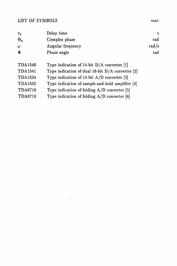
Symbol Description Unit
A Amplitude I
LlA Amplitude deviation I
AID Analog-to-Digital
Afoldback Ratio between amplifier bandwidth and system bandwidth I
Ab Amplitude of square wave I
Ac Amplitude of sine wave 1
Ad Attenuation component: index d 1
Ae Amplitude of error signal I
Af Amplitude of fundamental I A· J Amplitude level: index j I
Al Limiter constant I
Arms Root Mean Square amplitude value 1
As Amplitude of sine wave I
Astopband Stopband attenuation dB ATE Automatic Test Equipment
App Peak-to-peak amplitude I
An Operational Amplifier: index n I
Ao Output value of I-bit quantizer I
Aopenloop Open-loop amplification I B Full-Scale Value I
Bin Input number of bits I
Bo Most Significant Bit Value I
Bm mth Bit Value 1
Bn- 1 Least Significant Bit Value 1
xxix
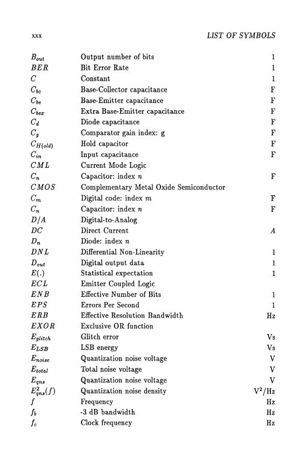
xxx LIST OF SYMBOLS
Bout Output number of bits 1
BER Bit Error Rate 1
C Constant 1
Cbc Base-Collector capacitance F
Cbe Base-Emitter capacitance F
Cbex Extra Base-Emitter capacitance F
Cd Diode capacitance F
Cg Comparator gain index: g F
CH(old) Hold capacitor F
Cin Input capacitance F
CML Current Mode Logic
Cn Capacitor: index n F
CMOS Complementary Metal Oxide Semiconductor
Cm Digital code: index m F
Cn Capacitor: index n F
DjA Digital-to-Analog
DC Direct Current A Dn Diode: index n
DNL Differential Non-Linearity 1
Dout Digital output data 1
E(.) Statistical expectation 1
ECL Emitter Coupled Logic ENB Effective Number of Bits 1 EPS Errors Per Second 1 ERB Effective Resolution Bandwidth Hz EXOR Exclusive OR function
Eglitch Glitch error Vs
ELSB LSB energy Vs
Enoise Quantization noise voltage V
Etotal Total noise voltage V
Eqns Quantization noise voltage V
E;ns(f) Quantization noise density V2jHz I Frequency Hz
Ib -3 dB bandwidth Hz
Ie Clock frequency Hz

LIST OF SYMBOLS xxxi
leomp
lin lose
Iqns
Is
Isig
IUGB
FSR GA G(z)
9m H(z) H(w) HS3
II It I /j.I
Ie Ieomp
Ileakage
lout
IRef
IEEE INL
io 10 12S
IT lin
J-FET J(z) k K(z)
Comparator -3 dB bandwidth
Input signal frequency
Oscillation frequency Quantization noise bandwidth
Sample frequency Signal bandwidth Unity Gain Bandwidth Full-Scale Range
Amplifier gain Transfer function Mutual transconductance
Transfer function
System transfer function High-speed bipolar oxide isolated process Unity gain bandwidth
Transition frequency
Current Current deviation As index Integrated Circuit Compensation current
Leakage current Output current Reference current Institute of Electrical and Electronic Engineers Integral Non-Linearity Base-Emitter reverse current Bias current index: 0 Inter IC Signal Standard Temperature-dependent current Input current
Junction Field Effect Transistor Transfer function
Hz
Hz Hz
Hz
Hz
Hz Hz
1
1
1
A/V 1
1
Hz
Hz
A A
1
A
A A
A
1 A A
A/degree C A
Boltzmann's constant Transfer function
1.38 X 10⁻²³ J /K As index 1
1
1
xxxii LIST OF SYMBOLS
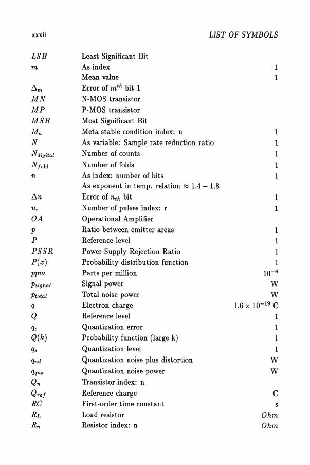
LSB Least Significant Bit
m As index 1 Mean value 1
Am Error of mth bit 1
MN N-MOS transistor
MP P-MOS transistor
MSB Most Significant Bit
Mn Meta stable condition index: n 1
N As variable: Sample rate reduction ratio 1
Ndigital Number of counts 1
NJoid Number of folds 1
n As index: number of bits 1 As exponent in temp. relation ~ 1.4 - 1.8
An Error of nth bit 1
nr Number of pulses index: r 1 OA Operational Amplifier
p Ratio between emitter areas 1
P Reference level 1
PSSR Power Supply Rejection Ratio 1
P(x) Probability distribution function 1
ppm Parts per million 10-6
Psignal Signal power W
Ptotal Total noise power W q Electron charge 1.6 x 10⁻¹⁹ C
Q Reference level 1
qe Quantization error 1
Q(k) Probability function (large k) 1
qs Quantization level 1
qnd Quantization noise plus distortion W
qqns Quantization noise power W
Qn Transistor index: n
QreJ Reference charge C RC First-order time constant s
RL Load resistor Ohm Rn Resistor index: n Ohm
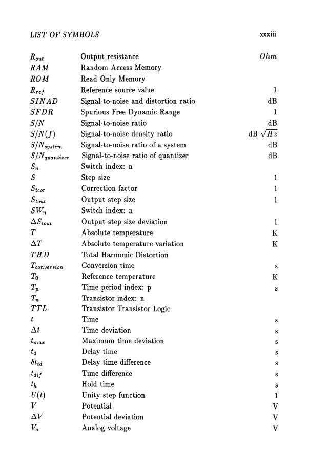
LIST OF SYMBOLS xxxiii
Rout Output resistance Ohm
RAM Random Access Memory
ROM Read Only Memory
Rre/ Reference source value 1 SINAD Signal-to-noise and distortion ratio dB
SFDR Spurious Free Dynamic Range 1 SjN Signal-to-noise ratio dB SjN(f) Signal-to-noise density ratio dB JHz
S/Nsystem Signal-to-noise ratio of a system dB
S / Nquantizer Signal-to-noise ratio of quantizer dB
Sn Switch index: n
S Step size 1
Stcor Correction factor 1
Stout Output step size 1 SWn Switch index: n
f:!l.stout Output step size deviation 1 T Absolute temperature K ~T Absolute temperature variation K THD Total Harmonic Distortion
Tconversion Conversion time s To Reference temperature K Tp Time period index: p s Tn Transistor index: n TTL Transistor Transistor Logic t Time s ~t Time deviation s tmax Maximum time deviation s td Delay time s 6ttd Delay time difference s
tdi/ Time difference s th Hold time s U(t) Unity step function 1 V Potential V ~V Potential deviation V Va Analog voltage V
xxxiv LIST OF SYMBOLS
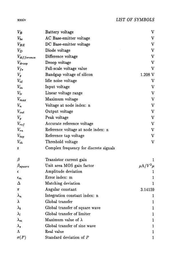
VB Battery voltage V
Vbe AC Base-emitter voltage V
VBE DC Base-emitter voltage V
VD Diode voltage V
Vdif ference Difference voltage V
Vdroop Droop voltage V
Vfs Full-scale voltage value V
Vg Bandgap voltage of silicon 1.208 V
~d Idle noise voltage V
~n Input voltage V
Vir Linear voltage range V
Vmax Maximum voltage V
Vn Voltage at node index: n V
Vout Output voltage V
Vp Peak voltage V
Vref Accurate reference voltage V
Vrn Reference voltage at node index: n V
lItap Reference tap voltage V
lith Threshold voltage V
z Complex frequency for discrete signals
{3 Transistor current gain 1
(3square Unit area MOS gain factor JlA/V2Jl f Amplitude deviation 1
fm Error index: m 1 ~ Matching deviation 1 11" Angular constant 3.14159
An Integration constant index: n 1
A Global transfer 1
Ab Global transfer of square wave 1
AI Global transfer of limiter 1
Am Maximum value of A 1
As Global transfer of sine wave 1
A Real value 1 u(P) Standard deviation of P 1
LIST OF SYMBOLS
w
TDA1540
TDAl541
TDA1534
TDA1535
TDA8716
TDA8718
Delay time
Complex phase
Angular frequency
Phase angle
Type indication of 14-bit D I A converter [1]
Type indication of dual 16-bit D I A converter [2]
Type indication of 14-bit AID converter [3]
Type indication of sample-and-hold amplifier [4}
Type indication of folding AID converter [5]
Type indication of folding AID converter [6]
xxxv
s rad
rad/s
rad

Preface
In this introduction an overview of the contents of this book will be given. Analog-to-digital (AID) and digital-to-analog (D I A) converters provide the link between the analog world of transducers and the digital world of signal processing, computing, and other digital data collection or data processing systems. Numerous types of converters have been designed that use the best technology available at the time a design is made. High-performance bipolar and MOS technologies result in high-resolution or high-speed AID and D I A converters that can be applied in digital audio and digital video systems. Furthermore, the high-speed bipolar technologies show an increase in conversion speed into the Giga Hertz range. Applications in these areas are, for example, in high-definition digital television and digital oscilloscopes. The availability of high-speed memory chips results in so-called "one-shot" memory applications in these oscilloscopes. In this book different techniques to improve the accuracy in high-resolution AID and D I A converters will be discussed. Also, special techniques to reduce the number of elements in highspeed AID converters by a repetitive use of comparators will be described.
In Chapter one the application of converters in systems will be discussed. H analog-to-digital and digital-to-analog converters are applied in discretetime systems it is important to perform these operations on frequency-bandlimited signals. In most cases filters are needed to limit the input and output spectrum of the analog signals. H no band limitation is performed, then aliasing of the analog signals into the signal band of interest can occur. General criteria that determine the overall system performance in the case of ideal converters are introduced and defined. Combinations of analog and digital filtering operations result in linear phase filtering over the band of interest. Such a linear phase filtering is very important in digital audio systems.
Performance definitions of converters are defined in Chapter two. The perfor-
xxxvii

xxxviii Preface
mance definitions must be unique for a specific parameter. Good parameter definitions of converters are very important in determining the final performance of a discrete-time system. Furthermore, these definitions can be used to compare the performance of different brands of converters. In particular, a good definition of the dynamic parameters of converters is needed. The application of converters in digital audio and digital video systems, for example, requires these dynamic specifications. Many converters that originally were designed for high-accuracy measurement system applications are not optimized for dynamic operations. In digital audio, for example, many specifications, which are important in instrumentation (such as offset, fullscale accuracy, temperature drift) are of minor value. The specific dynamic parameters must therefore be defined and related to important design parameters. Glitches in D I A converters introduce distortion in digital audio systems, while in video display systems fuzzy images are obtained.
After defining the important specifications of converters, good measurement set-ups and definitions are needed. In Chapter three attention is paid to measuring the static and dynamic performance of converters. Usually DC parameters can be measured with automatic test equipment and are well defined. Much attention has been paid to obtaining measurements and measurement set-ups which give the required parameter in a fairly simple way and use a well-defined test condition. One of the most important parameters to be determined in this way is the dynamic performance of a system. The dynamic range is determined by measuring the signal-to-noise ratio of a converter over half the sampling frequency. This signal-to-noise ratio must, in the case of a well-designed converter, be close to the theoretical value, which is defined over a bandwidth equal to half the sampling frequency. When large discrepancies are found, then this converter is not designed to operate under dynamic conditions. Sometimes it is possible to overcome some of the problems by adding external circuitry, which, for example, can be a deglitcher circuit to reduce the glitch of the converter or by adding data latches which perform the switching of the bit weights in a digital-to-analog converter at the same time moment.
A high-performance sample-and-hold amplifier in front of a parallel-type AID converter can improve at high frequencies the dynamic performance of this converter. The sampling of the analog signal in this way is performed by the sample-and-hold amplifier. The following AID converter only needs to have a good settling performance to the applied input signal step from the

Preface xxxix
sample-and-hold amplifier. Distortion introduced by timing uncertainties at high frequencies in the flash converter can be avoided in this way.
In general it can be said that the number of systems and circuits that can perform analog-to-digital conversion is much larger than the number of structures and basic solutions to digital-to-analog conversion. In Chapter four examples of high-speed analog-to-digital converters are discussed. Up until now the full-flash converter was considered the fastest converter type that can be designed. This, however, is only partly true. Due to the use of a large amount of components for example, in an 8-bit converter 255 comparators are needed to detect every code level the size of such a converter becomes large with respect to the time a signal needs to travel over the interconnection lines on a chip. In high-speed converters the time difference for signals traveling at the top of the converter structure with respect to signals traveling in the middle of the structure may become in the order of pico seconds. At high-input frequencies these time differences in signal transfer introduce distortion. Depending on input frequency and resolution of a converter, timing differences may not exceed pico second values. When taking into account that the transmission speed over the interconnection lines in an integrated circuit is about two-thirds of the speed of light, then 1 psec equals about 200 microns of interconnect. When the size of an analog-to-digital converter chip without sample-and-hold amplifier increases, it is practically impossible to match clock- and signal-line delays within the required timing accuracy. Therefore, improved converter systems with a reduced chip size using a continuous input-signal folding architecture overcome these problems. In a final system implementation of such a system, only zero crossings of the analog signal are important for the converter accuracy. To reduce the number of input amplifier-comparator stages in such a system, an interpolation of zero crossings is used. This system results in a compact very high-performance analog-to-digital converter structure. In an MOS technology switches and capacitors are the main design elements. The input signal can be stored
. on multiple capacitors and then a comparison is made to perform an AID conversion. Even two-step system solutions can be easily implemented in this structure.
High-speed converter systems depend on the availability of high-performance sample-and-hold amplifiers. Such systems are difficult to design, while furthermore the maximum sampling frequency and the accuracy of the system are determined by the performance of the sample-and-hold amplifier. In

xl Preface
digitally sampled (eg, full flash and folding A/D structures) systems mostly a much higher sampling clock can be applied without disturbing the analog signal path. In this way additional resolution and/or accuracy can be obtained by using oversampling, filtering, and subsampling techniques.
In high-speed analog-to-digital converters that are based on the full-flash or folding principles, the question about the relation between maximum analog input frequency and the bandwidth of the comparator-amplifier stages arises. In Chapter five an analysis that determines the relation between the maximum analog input frequency and the bandwidth of the comparatoramplifier stages is performed. Furthermore it will be shown from this analysis that a limited analog bandwidth of the system results in third-order signal distortion. This distortion can fold signals back into the baseband of the converter and results in a reduction of the signal-to-noise ratio of the system. The maximum analog input frequency will be defined as that input frequency for which the signal-to-noise ratio is reduced by a value equal to half the least significant bit. The number of effective bits as a function of input frequency will be used as an accurate measure for the performance of high-speed analog-to-digital converters. A second analysis about the decision failure of comparators in flash-type converters is performed. This analysis gives insight in the relation between the bit error rate (HER) of a comparator as a function of the gain-bandwidth product of a technology. Comparator stages can be optimized for a minimum error.
In high-accuracy analog-to-digital and digital-to-analog converters the accuracy with which the binary weighting of the bit weights is performed is an important design criterion. In Chapters six and seven generally applicable methods to obtain high-accuracy converters will be introduced. These methods will mainly use a combination of accuracy introduced by matched elements and a dynamic method to improve the limited passive accuracy. Resistor or capacitor matching in integrated circuits limits the resolution of converters based on these elements to about ten to twelve bits. Trimming methods can be used to overcome this problem. These trimming methods, however, are expensive, while in addition changes of the trimmed elements due to time or temperature variations destroy the accurate trimming of the converter. In MOS technologies accuracy is obtained by matching binary weighted capacitor banks. Accuracies of ten to twelve bits are possible without trimming.
Preface xli
When monotonicity of a converter is the most important design criterion then special system configurations are possible. Solutions based on current swapping or voltage division will be described. These systems are inherently monotonic while overall linearity is limited.
When the absolute accuracy in a converter is required, then special systems are needed. Systems which convert the digital value into an accurate time need a limited amount of accurate elements. However, speed is limited, while systems with higher sampling rates suffer from extremely high clock frequencies which result in high-frequency signal radiation.
To overcome these problems a combination of passive and active matching of components will be used. The first method combines accurate passive division with a time interchanging concept to obtain a very high weighting accuracy without using accurate elements. Furthermore, this method is independent of element aging and remains accurate over a large temperature range. Examples of 14- and 16-bit digital-to-analog and analog-to-digital converters will be given that use this special method. The system is not limited to bipolar technologies, although at this moment only examples of bipolar implementations exist. In an MOS technology calibration of current sources can be used to obtain a segmented converter structure. Such a structure is less sensitive to element matching, while the calibration of the individual current sources makes the system independent of element aging and less temperature-sensitive. The gate capacitance of an MOS device is used to store the error signal information that is needed to calibrate the bit current sources.
In high-accuracy analog-to-digital converters the analog input signal must be sampled and kept constant during the time the conversion takes place. Highresolution and high-accuracy sample-and-hold amplifiers are a key element for analog-to-digital conversion in, for example, digital audio. Examples of high-speed sample-and-hold amplifiers using a bipolar or CMOS technology will be described in Chapter eight. These systems are very suitable for medium-resolution high-speed AjD converters using a two-step conversion method.
For the most part open-loop systems are used in high-speed sample-and-hold amplifiers to avoid stability problems and obtain the maximum bandwidth of such a system.

xlii Preface
Furthermore, a high-resolution design using a bipolar technology and employing an overall feedback will be described. This sample-and-hold amplifier uses high-performance operational amplifiers with improved frequency compensation techniques. A specially designed all-NPN class-B output stage with switching capability completes the design.
Low-noise high-stability reference sources are a basic element in converters. Different methods to obtain accurate and temperature insensitive reference sources will be given. These circuits use special techniques to fabricate zener diodes with low-temperature coefficients and a good long-term stability. In integrated circuits reference sources are designed that are based on the bandgap voltage of silicon. The temperature dependence of the bandgap voltage reference sources is small, but in the case of 16-bit converters this temperature stability is not good enough. Therefore, systems that use a second-order temperature compensation will be discussed in Chapter nine. The noise analysis of these systems is performed, and data will be given on the signal-to-noise ratio. Methods to reduce the noise as a function of frequency will be discussed.
In Chapters ten and eleven examples of noise-shaping techniques to improve the dynamic range of a system are described. Such techniques are very useful when speed can be exchanged with accuracy or with the wordlength used in a system.
An ultimate of the noise-shaping techniques are the well-known sigma-delta AID and D I A converters which basically use a noise-shaping filter in cooperation with a quantizer and a I-bit D I A or AID converter stage. Such a I-bit converter is extremely linear, which results in a very good differential linearity of such a converter. The most important design criteria and limitations will be given. At the moment the dynamic range of a system must be increased but the maximum clock speed in the system cannot be enlarged, then a multi-bit D / A converter can be used in the feedback loop. At that moment, however, the linearity of the D/A converter determines the overall linearity of the converter. Therefore, dynamic element matching or self-calibration techniques are required to obtain this very high linearity. The root locus method can be used successfully to determine the stability of noise-shaping coders. Especially when a higher-order noise-shaping filter is used, the stability analysis gives an insight in the operation of the system

Preface xliii
when large input signals are applied. A noise-shaping coder is said to be stable when an idle pattern at half the sampling frequency is present under nearly all input signal conditions. Different architectures will be described which introduce a high-order noise-shaping filter architecture without running into a stability problem. A special system that uses a signal-Ieveldependent filtering order introduces a kind of feed-forward coupling in the filtering function. At low-level input signals a high-order filtering function is present, but at the moment the signal in the loop increases in amplitude, the filter order is reduced. In this way a very good optimum between filter order and stability of operation is obtained. Examples of designed 16- to 20-bit D/A converters using I-bit or multi-bit D/A converters will be described. Finally an example of a 5-digit digital voltmeter system to complete this Chapter will be given.
Many circuits given in this book use bipolar technologies. Most of the designs were implemented in a standard 10 micron minimum-size double-metal process. The transition frequency of the transistors in this process is between 350 MHz and 400 MHz. In the high-speed folding and interpolation analogto-digital converter, an oxide-isolated bipolar process with a transition frequency between 7 and 8 GHz is used. The minimum emitter size of the transistors in this technology is 2 x 3 micron. The MOS circuits are implemented in 1- to 2-p. gate-length complementary MOS devices. Mostly such a technology is optimized for digital applications. Therefore, the systems must be designed to be rather insensitive to MOS parameter variations and to be incorporated onto a large digital signal-processing chip. In that case special attention must be paid to crosstalk problems between the digital system part and the mostly sensitive analog part of the AID and D I A converter.
Components in an integrated circuit are best matched when they are placed close to each other. Furthermore, these devices must be placed on chip using an isothermal boundary. When more devices such as transistors or resistors must have a very good matching, care must be taken that neighboring, not active elements are placed at the edges of the layout of such a system. In this wayan improvement in matching between the individual elements of the array is obtained. Furthermore, the non-linearity of, for example, diffused base resistors can be compensated for using a proper island connection or splitting-up the resistor into parts from which each part is compensated by connecting the island to every individual resistor. These technology-oriented subjects are mostly shortly discussed. More information can be obtained

xliv Preface
from proper literature.
During the writing of this book an attempt has been made to discuss the most important parameters and design criteria and giving worked-out examples of practical circuits and systems. On the other hand, no attempt has been made to be complete and cover all subjects in detail. By including practically worked-out examples, which in a number of cases are products supplied by semiconductor manufacturers, the reader gets familiar with design problems and practical system implementations under real conditions. For the most part, these implementations differ quite a lot from the basic system solution.


