Hindawi Publishing CorporationActive and Passive Electronic ComponentsVolume 2007, Article ID 69515, 4 pagesdoi:10.1155/2007/69515
Research ArticleIntegrated Balanced BPSK Modulator forMillimeter Wave Systems
Ashok Mittal1, 2 and Asok De1
1 Delhi College of Engineering, University of Delhi, Delhi 110 042, India2 Central Research Laboratory, Bharat Electronics Ltd, Ghaziabad 201 010, India
Received 28 April 2007; Accepted 14 September 2007
Recommended by Spartak Gevorgian
This paper details the design of integrated balanced PSK modulator using finline coplanar line hybrid junction. The PSK signaloutput is in suspended stripline with incident wave carrier in finline. Schottky barrier Diode MA4E2037 has been used for mod-ulation. The balanced configuration offers high isolation between the carrier input port and the modulated carrier output portand thus the pulse width variations and amplitude deviations are suppressed. An insertion loss imbalance of ±1.5 dB with anaverage loss of 2 dB in the two switching states has been achieved over 38.9 to 40 GHz. The phase imbalance is ±10 degrees withphase switching from 180 to 199 degrees As the PSK output signal is in suspended stripline, two BPSK modulators can be easilycombined together to work as QPSK modulator.
Phase-shift-keying (PSK) modulators are been widely used indigital communications. PSK modulators are mainly dividedinto two different types: a balanced or a double-balancedtype and a path-length modulator (unbalanced) type [1].
Path length modulators are realized as reflection ortransmission-type modulators. The reflection-type modu-lators are constructed by using either a waveguide circula-tor or using an MIC 3 dB branch-line hybrid coupler. Thetransmission-type modulators are realized using two mi-crostrip lines with different line lengths and two switchingdiodes. In the path-length modulator, amplitude variationsand jitter occur in PSK waveforms due to the path-length dif-ference.
On the other hand, the balanced modulator using equalpath lengths realizes PSK waveforms without jitter andachieves good isolation between the carrier input port andthe modulated carrier output port, and a good PSK wave-form in a wide frequency band. Furthermore, the balancedmodulator can be easily fabricated by the printed circuit MICtechniques, thus giving high yield and repeatability.
The modulators developed have high isolation betweenthe carrier input port and the modulated carrier output port.
The pulse width variations and amplitude deviations are sup-pressed due to the balanced configuration used.
Phase-shift keying (PSK) describes the modulation tech-nique that alters the phase of the carrier. Mathematically,
s(t) = sin(2π fct + φ(t)
). (1)
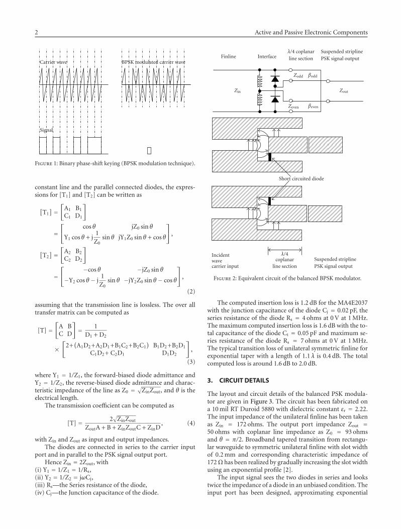
Binary phase-shift keying (BPSK) has only two phases: 0and π. It is, therefore, a type of ASK with f (t) taking the val-ues −1 or 1 (Figure 1 ), and its bandwidth is the same as thatof ASK. Phase-shift keying offers a simple way of increasingthe number of levels in the transmission without increasingthe bandwidth by introducing smaller phase shifts.
2. TRANSMISSION LOSS CALCULATIONS
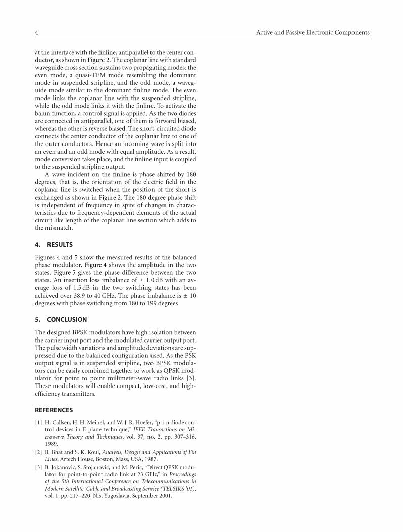
The basic planar finline circuit of BPSK modulator or 180degrees digital phase shifter is similar to that of millimeter-wave balanced finline mixers. Figure 2 shows the equivalentcircuit of the hybrid junction with Schottky Barrier DiodesMA4E2037 mounted across the finline coplanar line hybridjunction. The PSK signal output is in suspended stripline us-ing a coaxial K connector. If we take [T1] and [T2] as thetransfer matrix of the two switching states with distributed
constant line and the parallel connected diodes, the expres-sions for [T1] and [T2] can be written as
[T1] =
[A1 B1
C1 D1
]
=⎡
⎣cos θ jZ0 sin θ
Y1 cos θ + j1
Z0sin θ jY1Z0 sin θ + cos θ
⎤
⎦ ,
[T2] =
[A2 B2
C2 D2
]
=⎡
⎣−cos θ −jZ0 sin θ
−Y2 cos θ − j1
Z0sin θ −jY2Z0 sin θ − cos θ
⎤
⎦ ,
(2)
assuming that the transmission line is lossless. The over alltransfer matrix can be computed as
[T] =[
A BC D
]
= 1D1 + D2
×[
2+(A1D2 +A2D1 +B1C2 +B2C1
)B1D2 +B2D1
C1D2 + C2D1 D1D2
]
,
(3)
where Y1 = 1/Z1, the forward-biased diode admittance andY2 = 1/Z2, the reverse-biased diode admittance and charac-teristic impedance of the line as Z0 =
√ZinZout, and θ is the
electrical length.The transmission coefficient can be computed as
[T] = 2√
ZinZout
ZoutA + B + ZinZoutC + ZinD, (4)
with Zin and Zout as input and output impedances.The diodes are connected in series to the carrier input
port and in parallel to the PSK signal output port.Hence Zin = 2Zout, with
(i) Y1 = 1/Z1 = 1/Rs,(ii) Y2 = 1/Z2 = jωCj,(iii) Rs—the Series resistance of the diode,(iv) Cj—the Junction capacitance of the diode.
Zin Zout
Zodd βodd
Zeven βeven
Short circuited diode
Finline Interfaceλ/4 coplanarline section
Suspended striplinePSK signal output
Incidentwavecarrier input
λ/4coplanar
line sectionSuspended striplinePSK signal output
Figure 2: Equivalent circuit of the balanced BPSK modulator.
The computed insertion loss is 1.2 dB for the MA4E2037with the junction capacitance of the diode Cj = 0.02 pF, theseries resistance of the diode Rs = 4 ohms at 0 V at 1 MHz.The maximum computed insertion loss is 1.6 dB with the to-tal capacitance of the diode Ct = 0.05 pF and maximum se-ries resistance of the diode Rs = 7 ohms at 0 V at 1 MHz.The typical transition loss of unilateral symmetric finline forexponential taper with a length of 1.1 λ is 0.4 dB. The totalcomputed loss is around 1.6 dB to 2.0 dB.
3. CIRCUIT DETAILS
The layout and circuit details of the balanced PSK modula-tor are given in Figure 3. The circuit has been fabricated ona 10 mil RT Duroid 5880 with dielectric constant εr = 2.22.The input impedance of the unilateral finline has been takenas Zin = 172 ohms. The output port impedance Zout =50 ohms with coplanar line impedance as Z0 = 93 ohmsand θ = π/2. Broadband tapered transition from rectangu-lar waveguide to symmetric unilateral finline with slot widthof 0.2 mm and corresponding characteristic impedance of172Ω has been realized by gradually increasing the slot widthusing an exponential profile [2].
The input signal sees the two diodes in series and lookstwice the impedance of a diode in an unbiased condition. Theinput port has been designed, approximating exponential
A. Mittal and A. De 3
0.1
0.25 2
0.253.556
9
3.556
3.556
0.254
7.112
3.556
3.556
4
4
1
2
0.250.5
0.25
Schottkydiodes
Figure 3: Layout and circuit details of the balanced BPSK modulator.
10 dB/
20 dB
20 dB
1∇
1∇
2∇
2∇
< 0 dB
< 0 dB
∇2: −2.305 dB38.9 GHz
−1.936 dB39.725 GHz
∇1:
MAT1%SMC10 kFIL
CPL
b12a2Ia1PCI
CAI
CH1 S21/ dB MAG 10 dB/ REF 0 dB
∇2: −1.189 dB38.9 GHz−1.107 dB39.725 GHz
∇1:
CH1 S21/ dB MAG 10 dB/ REF 0 dB
Start 38.9 GHz 100 MHz/ Stop 40 GHz
Date: 25.APR.07 10:46:54
Figure 4: Insertion loss imbalance of the balanced BPSK modula-tor.
dependence of taper to symmetrical unilateral finline tomatch the RF impedance of the diodes at the junction. Bal-anced action is achieved by a 180 degree hybrid formed atthe junction of the finline, coplanar line, and suspended sub-strate transmission line due to the excitation of their cross-polarized electric fields. The diodes are switched to achievethe 180 degree phase-shift keying according to the inputmodulating wave through a low-pass filter. The balun is theactual phase-shifter circuit with switching between the two
450◦
−450◦
1∇
2∇
< 0◦
∇2: 199.7◦38.999 GHz
185.7◦39.725 GHz
∇1:
MAT1%SMC10 kFIL
CPL
b12a2Ia1PCI
CAI
CH1 S21− LINφ 90◦/
90◦/
REF 0◦
Start 38.9 GHz 100 MHz/ Stop 40 GHz
Date: 25.APR.07 10:29:09
Figure 5: Phase shift between the two switching states of the bal-anced BPSK modulator.
states. The transitions connect the phase shifter with thewaveguide system, while the low-pass filter links the diodesto the control signal.
The balun is formed by a λ/4 coplanar line with stan-dard rectangular waveguide cross section. One end is con-nected to the finline, while the other is connected tothe suspended stripline which has a reduced cross section tosuppress higher-order mode propagation. The Schottky bar-rier diodes MA4E2037 are mounted across the coplanar line
4 Active and Passive Electronic Components
at the interface with the finline, antiparallel to the center con-ductor, as shown in Figure 2. The coplanar line with standardwaveguide cross section sustains two propagating modes: theeven mode, a quasi-TEM mode resembling the dominantmode in suspended stripline, and the odd mode, a waveg-uide mode similar to the dominant finline mode. The evenmode links the coplanar line with the suspended stripline,while the odd mode links it with the finline. To activate thebalun function, a control signal is applied. As the two diodesare connected in antiparallel, one of them is forward biased,whereas the other is reverse biased. The short-circuited diodeconnects the center conductor of the coplanar line to one ofthe outer conductors. Hence an incoming wave is split intoan even and an odd mode with equal amplitude. As a result,mode conversion takes place, and the finline input is coupledto the suspended stripline output.
A wave incident on the finline is phase shifted by 180degrees, that is, the orientation of the electric field in thecoplanar line is switched when the position of the short isexchanged as shown in Figure 2. The 180 degree phase shiftis independent of frequency in spite of changes in charac-teristics due to frequency-dependent elements of the actualcircuit like length of the coplanar line section which adds tothe mismatch.
4. RESULTS
Figures 4 and 5 show the measured results of the balancedphase modulator. Figure 4 shows the amplitude in the twostates. Figure 5 gives the phase difference between the twostates. An insertion loss imbalance of ± 1.0 dB with an av-erage loss of 1.5 dB in the two switching states has beenachieved over 38.9 to 40 GHz. The phase imbalance is ± 10degrees with phase switching from 180 to 199 degrees
5. CONCLUSION
The designed BPSK modulators have high isolation betweenthe carrier input port and the modulated carrier output port.The pulse width variations and amplitude deviations are sup-pressed due to the balanced configuration used. As the PSKoutput signal is in suspended stripline, two BPSK modula-tors can be easily combined together to work as QPSK mod-ulator for point to point millimeter-wave radio links [3].These modulators will enable compact, low-cost, and high-efficiency transmitters.
REFERENCES
[1] H. Callsen, H. H. Meinel, and W. J. R. Hoefer, “p-i-n diode con-trol devices in E-plane technique,” IEEE Transactions on Mi-crowave Theory and Techniques, vol. 37, no. 2, pp. 307–316,1989.
[2] B. Bhat and S. K. Koul, Analysis, Design and Applications of FinLines, Artech House, Boston, Mass, USA, 1987.
[3] B. Jokanovic, S. Stojanovic, and M. Peric, “Direct QPSK modu-lator for point-to-point radio link at 23 GHz,” in Proceedingsof the 5th International Conference on Telecommunications inModern Satellite, Cable and Broadcasting Service (TELSIKS ’01),vol. 1, pp. 217–220, Nis, Yugoslavia, September 2001.