Integrated Circuit Design with the MOSFET 9.1 MOSFET Current Mirrors 9.2 Amplifier Configurations for MOSFET Integrated Circuits The MOSFET has become more popular in circuit design in the last decade, especially for mixed-signal circuits that combine both digital and analog circuits on a single chip. With the improvements in high-frequency performance, the MOSFET can compete with the BJT up to frequencies in the low GHz range. Of course, the heterojunction BJT can operate at much higher frequencies than this, approaching frequencies of 100 GHz. This chapter will consider several configurations of amplifying stages used in MOSFET amplifier design. Each configuration is analyzed in terms of mid- band voltage gain, upper corner frequency, and the size of the output active region. Design of MOSFET circuits is considerably different from the design of BJT circuits. For example, the dimensions of the channel are used as part of the design procedure in MOSFET circuits. The width of the channel affects the transconductance, the output resistance and capacitance, and the midband voltage gain of the stage. The specification of channel width is often one step in the design of a MOSFET amplifier stage. In digital circuits, the width and the length are generally of the same order of magnitude. In amplifier design, the dimension of channel width may be hundreds of times greater than the channel length to achieve high values of voltage gain. Such considerations are not necessary in BJT amplifier design, which provides one reason for cov- ering BJT design in a separate chapter. The next chapter will consider the BJT. One circuit that is very significant in IC design is the current mirror. This circuit not only provides bias for amplifier stages, it also provides an incremental resistive load for various amplifier stages. The first section of this chapter will discuss some basic configurations of this important circuit, before moving to various amplifier configurations. DEMONSTRATION PROBLEM The circuit shown is a common-source amplifier with a current mirror load. If K n = µ n C ox W n /2 L n = 0.12 mA/V 2 , K p = µ p C ox W p /2 L p = 0.1 mA/V 2 , λ n = λ p = 0.01 V −1 , and V Tn =−V Tp = 1 V, find V 1 to set V DSQ1 = 2.5 V. Calculate the midband voltage gain of the amplifier. 263
The MOSFET has become more popular in circuit design in the last decade,especially for mixed-signal circuits that combine both digital and analog circuitson a single chip. With the improvements in high-frequency performance, theMOSFET can compete with the BJT up to frequencies in the low GHz range.Of course, the heterojunction BJT can operate at much higher frequencies thanthis, approaching frequencies of 100 GHz.
This chapter will consider several configurations of amplifying stages usedin MOSFET amplifier design. Each configuration is analyzed in terms of mid-band voltage gain, upper corner frequency, and the size of the output activeregion.
Design of MOSFET circuits is considerably different from the design ofBJT circuits. For example, the dimensions of the channel are used as part ofthe design procedure in MOSFET circuits. The width of the channel affectsthe transconductance, the output resistance and capacitance, and the midbandvoltage gain of the stage. The specification of channel width is often one stepin the design of a MOSFET amplifier stage. In digital circuits, the width andthe length are generally of the same order of magnitude. In amplifier design,the dimension of channel width may be hundreds of times greater than thechannel length to achieve high values of voltage gain. Such considerations arenot necessary in BJT amplifier design, which provides one reason for cov-ering BJT design in a separate chapter. The next chapter will consider theBJT.
One circuit that is very significant in IC design is the current mirror. Thiscircuit not only provides bias for amplifier stages, it also provides an incrementalresistive load for various amplifier stages. The first section of this chapter willdiscuss some basic configurations of this important circuit, before moving tovarious amplifier configurations.
D E M O N S T R A T I O N P R O B L E M
The circuit shown is a common-source amplifier with a current mirror load. If Kn =µnCoxWn/2Ln = 0.12 mA/V2, K p = µpCoxWp/2L p = 0.1 mA/V2, λn = λp = 0.01 V−1, andVT n = −VT p = 1 V, find V1 to set VDSQ1 = 2.5 V. Calculate the midband voltage gain of theamplifier.
263
P1: FCH/SPH P2: FCH/SPH QC: FCH/UKS T1: FCH
pb139B-09 ZP042-Sam.cls February 13, 2002 18:42
264 C H A P T E R 9 I N T E G R A T E D C I R C U I T D E S I G N W I T H T H E M O S F E T
5 V
M3 M2
M18 kΩ
vin
V1
VDSQ1vout
Amplifier for DemonstrationProblem
This problem requires a knowledge of the dc current versus voltage relationships of theMOSFETs to find the bias voltage, V1. A knowledge of the incremental equivalent circuit forthe MOSFET is needed to calculate the midband voltage gain.
9.1 MOSFET Current Mirrors
I M P O R T A N T Concepts
1. A simple MOSFET current mirror is constructed in the same configuration asthat of the BJT current mirror.
2. The ratio of output to input current can be determined by the aspect ratios of thetwo devices.
3. The Wilson current mirror can be used to achieve higher output impedance forthe output device.
The BJT current mirror was developed in the 1960s for use in op amp circuits. As theMOSFET increased in capability, the MOSFET current mirror evolved from the BJT circuit.MOSFET current mirrors operate on similar principles to the BJT mirrors to be discussedin Chapter 10 and use similar configurations. One advantage of MOSFET current mirrorsover BJT mirrors is that the MOS devices draw zero control current. The BJT stages exhibitsmall errors due to the finite base currents required. On the other hand, the matching ofthreshold voltages on MOS devices is generally not as good as the VB E matching of bipolardevices. Since BJT mirrors require additional considerations beyond those of MOSFETmirrors, a more thorough discussion of this circuit appears in Chapter 10.
Figure 9.1 shows a simple nMOS current mirror consisting of two matched devices,M1 and M2. This current mirror may be used to create a constant bias current for an ICamplifier stage. Integrated circuits provide the capability of matching device characteristicsquite closely and the current mirror takes advantage of this capability. In the circuit ofFig. 9.1, the current Io is intended to be equal to Iin. Although not shown in the figure, theexternal circuit through which Io flows connects to the drain of M2. The current Iin equalsthe drain current of M1 whereas Io is the drain current of M2.
Device M1 is in its active region, since drain current is flowing and the drain voltageequals the gate voltage. With VDS2 sufficiently positive to put M2 in the active region, the
P1: FCH/SPH P2: FCH/SPH QC: FCH/UKS T1: FCH
pb139B-09 ZP042-Sam.cls February 13, 2002 18:42
S E C T I O N 9 . 1 M O S F E T C U R R E N T M I R R O R S 265IoIin
M1 M2
VDS1 VGSVDS2
+
— Figure 9.1A simple nMOS current mirror(sink).
ratio of output current, Io, to input current, Iin, can be expressed as
Io
Iin=
[L1W2
L2W1
] [VGS − VT 2
VGS − VT 1
]2 [1 + λ2(VDS2 − VDS P2)
1 + λ1(VDS1 − VDS P1)
] [µ2Cox2
µ1Cox1
](9.1)
In ICs, it is possible to match devices so that µ1Cox1 = µ2Cox2, VT 1 = VT 2, and λ1 ≈ λ2.With these conditions satisfied, Eq. (9.1) can be written as
Io
Iin=
[L1W2
L2W1
] [1 + λ(VDS2 − VDS P2)
1 + λ(VDS1 − VDS P1)
](9.2)
As a result of the connection between gate and source of M1, VDS1 = VGS and, sinceVDS P1 = VGS − VT 1, we can simplify the denominator of Eq. (9.2) further. We can express[1 + λ(VDS1 − VDS P1)] as
[1 + λ(VGS − VGS + VT 1)] = 1 + λVT 1
Finally, if we limit the output voltage such that VDS2 = VDS1, Eq. (9.2) reduces to
Io
Iin= L1W2
L2W1(9.3)
This equation indicates that in the simple MOSFET current mirror, the ratio of Io to Iin maybe scaled to any desired value by scaling the aspect ratios (W/L) of the devices.
There are three effects that cause the MOSFET current mirror performance to differfrom that predicted by Eq. (9.3). These are:
1. Channel length modulation as VDS 2 changes, as predicted by Eq. (9.2)
2. Threshold voltage mismatch
3. Imperfect geometrical matching
E X A M P L E 9.1
Assume that a matched pair of MOSFETs are used in the current mirror of Fig. 9.1 withvalues of λ = 0.032 V−1, µCox = 70 µA/V2, W/2L = 10, and VT = 0.9 V. If a 5-V sourcein series with a resistor, R, is connected to the drain of M1 to create the input current,calculate the value of R needed to create an input current of 100 µA. Calculate the outputcurrent when VDS 2 = 3 V.
P1: FCH/SPH P2: FCH/SPH QC: FCH/UKS T1: FCH
pb139B-09 ZP042-Sam.cls February 13, 2002 18:42
266 C H A P T E R 9 I N T E G R A T E D C I R C U I T D E S I G N W I T H T H E M O S F E T
SOLUTION From the equation for drain current in the active region we write
ID1 = µCoxW
2L[VGS − VT ]2[1 + λ(VDS1 − VDS P1)]
Since VDS1 = VGS and VDS P1 = VGS − VT , this equation can be expressed as
ID1 = 100 = 700 [VGS − 0.9]2 [1 + 0.032 × 0.9]
We can now solve for the value of VGS to result in the specified drain current. This value isVGS = 1.27 V. The resistance needed to create 100 µA of drain current is
R = 5 − VDS1
ID1= 5 − 1.27
0.1= 37.3 k
The output current is calculated from
ID2 = µCoxW
2L[VGS − VT ]2 [1 + λ(VDS2 − VDS P2)]
In this case, VDS2 − VDS P2 = VDS2 − (VGS − VT ) = 3 − 1.27 + 0.9 = 2.63 V. The outputcurrent is then Io = 104 µA.
A MOSFET version of the BJT Wilson current mirror, discussed in Chapter 10, maybe used to reduce the output compliance error of the mirror. Figure 9.2 illustrates such annMOS mirror.
Iin Io
M1
+VDD
R
M2
M0
Figure 9.2nMOS version of the Wilsoncurrent mirror.
For matched devices, the current Iin may be expressed as
Iin = VDD − 2VGS
R(9.4)
where VGS is the gate-to-source voltage of all three devices. The output current is then
Io = Iin
[L1W2
L2W1
](9.5)
The voltage at the drain of M2 remains constant at a value of VGS , keeping Io constant, asthe output voltage at the drain of M0 varies over a large range. This stage has a higher outputimpedance than that of the simple current mirror because it has a source impedance. DeviceM2 presents an impedance between drain and ground that equals 1/gm2, thus increasingthe output impedance of M0. A higher output impedance leads to a smaller current changewith output voltage.P R A C T I C E Problems
9.1 For the finished designof Example 9.1, calculatethe output current whenVDS2 = 4 V. Ans: 107 µA.9.2 At what voltage mustVDS2 be in the currentmirror of Example 9.1 tocause an output current of102 µA? Ans: 2.37 V.9.3 Using the deviceparameters of Example 9.1,select the resistance R ofthis example to lead to anoutput current of 180 µAwhen VDS2 = 4 V.Ans: R = 22.3 k.
It is also possible to create current mirror sources with almost identical performance tothese sinks by using pMOS devices. Figure 9.3 shows a simple mirror and a Wilson-typemirror using pMOS devices. Although more complex current mirrors are sometimes used
Io
+VDD
R
M0
M2M1
+VDD
R
M2M1
Io
IinIin
Figure 9.3Current sources: (a) simplemirror, (b) Wilson mirror.
P1: FCH/SPH P2: FCH/SPH QC: FCH/UKS T1: FCH
pb139B-09 ZP042-Sam.cls February 13, 2002 18:42
S E C T I O N 9 . 2 A M P L I F I E R C O N F I G U R A T I O N S F O R M O S F E T I N T E G R A T E D C I R C U I T S 267in critical circuit design, the remainder of this chapter will apply the simple mirror of thissection.
1. Most MOSFET IC amplifier stages do not use a resistor as the load for theamplifying stage.
2. The load is generally created by one or more other MOS devices. These devicesare called active loads.
3. Active load stages can lead to very high voltage gains.
4. The ratio of channel width to channel length, called the aspect ratio, is quitesignificant in MOSFET circuit design.
In amplifier design, MOS circuits have become increasingly important, but not to theextent of CMOS digital circuits. Many of the MOSFET designs are nMOS or pMOS cir-cuits rather than CMOS circuits, but may be referred to as CMOS designs, because anestablished CMOS process is used to create the design even though no devices appear inthe complementary or CMOS configuration. P R A C T I C E Problem
9.4 A MOSFET has valuesof gm = 500 µA/V andrds = 130 k at ID =120 µA. Approximate thevalues of gm and rds for thisdevice at ID = 1 mA.Ans: gm = 1.44 mA/V,rds = 15.6 k.
Whereas digital circuit design almost eliminates the need for resistors or capacitors,analog circuit design may use resistors or capacitors in the design of amplifiers. It is usefulto minimize the need for these elements, since they may occupy spaces in which tens orhundreds of MOS devices may fit. In the next few subsections we will discuss MOSFETamplifier configurations. Before proceeding to these amplifiers, some useful relations forthe MOSFET will be tabulated. These are written in terms of an nMOS device in Table 9.1and were derived in Chapter 6.
9.2.1 SIMPLE AMPLIFIER STAGESA simple stage that can produce a controlled voltage gain is the diode-connected load stage,shown in Fig. 9.4. The numbers in circles represent the node numbers to be used in a later
Table 9.1 Useful Relations for an nMOS Device
DC Equations
Veff = VGS − VT Positive for triode or active regionZero or negative for subthreshold or cutoff
VDS P = VGS − VT = Veff Drain-source pinchoff voltageBorders triode and active region
ID = µCoxWL
[(VGS − VT )VDS − V 2
DS2
]Triode region
ID = µCoxW2L [VGS − VT ]2[1 + λ(VDS − Veff)] Active region
Small-Signal Equations
gm = √2µCox(W/L)ID = 2ID
VeffTransconductance
rds = 1λID P
Drain-source resistance
P1: FCH/SPH P2: FCH/SPH QC: FCH/UKS T1: FCH
pb139B-09 ZP042-Sam.cls February 13, 2002 18:42
268 C H A P T E R 9 I N T E G R A T E D C I R C U I T D E S I G N W I T H T H E M O S F E T
VDD
M2 2/1
M1 72/1
V1
V2
G1D1, S2
S1, D2, G2
(a)
(b)
vin
vout
3
4
2
1
vingm1vgs1 gm2vgs2
gs2vs2
rds1 rds2 vout
Figure 9.4(a) An amplifier with adiode-connected load.(b) Equivalent circuit.
simulation. This amplifier configuration demonstrates several important points relating togeneral MOSFET IC amplifier design. The transconductance term, gs2, accounts for thebody effect as the source to body voltage changes in device M2.
The amplifier can be treated as a gain stage, M1, driving a load impedance where theload impedance is that looking into the source of M2. Figure 9.5 shows the model for M2used to calculate the impedance at the source terminal. The impedance, RS2, looking intoS2 can be found by assuming that a voltage, vs2, is applied to S2. The resulting current iscalculated and divided into vs2 to find RS2.
With the gate voltage of M2 tied to ground, the gate-to-source voltage reduces tovgs2 = vg2 − vs2 = −vs2. When vs2 is applied to the source of M2, the current into thisterminal is
is2 = gm2vs2 + gs2vs2 + vs2
rds2
vs2
gm2vgs2G2
D2
S2
gs2vs2
rds2
is2
Figure 9.5Circuit used for impedancecalculation.
P1: FCH/SPH P2: FCH/SPH QC: FCH/UKS T1: FCH
pb139B-09 ZP042-Sam.cls February 13, 2002 18:42
S E C T I O N 9 . 2 A M P L I F I E R C O N F I G U R A T I O N S F O R M O S F E T I N T E G R A T E D C I R C U I T S 269The impedance looking into this terminal is then
RS2 = vs2
is2= 1
gm2 + gs2 + gds2(9.6)
where gds2 = 1/rds2.The midband voltage gain is found by recognizing that device M1 sees this load in
parallel with its own output impedance, rds1. This parallel resistance is the output resistance,Rout, which can be expressed as
Rout = rds1 ‖ RS2 = 1
gm2 + gs2 + gds2 + gds1(9.7)
The midband voltage gain is then
AM B = −gm1 Rout = − gm1
gm2 + gs2 + gds2 + gds1(9.8)
Typically, the largest term in the denominator will be gm2, which allows the gain to beapproximated by
AM B ≈ −gm1
gm2(9.9)
For example, a 1-µ device (L = 1µ) may have values of gm = 0.2 mA/V, gs =0.022 mA/V, and gds = 0.001 mA/V, which leads to a 12% error in the approximation ofEq. (9.9).
Examination of Eq. (9.9) shows that, for higher gains, gm1 must be much larger thangm2, which can be accomplished by controlling the aspect ratios (W/L) of the two devices.The approximate variation of gain with device scaling can be derived from a considerationof the equation for transconductance in the active region. This equation is found fromTable 9.1 and is
gm =√
2µnCox(W/L)ID (9.10)
Since the drain currents of both devices are equal, the voltage gain approximation ofEq. (9.9) can now be written as
AM B ≈ −√
2µnCox(W1/L1)ID√2µnCox(W2/L2)ID
= −[
(W1/L1)
(W2/L2)
]1/2
(9.11)
It can be seen from Eq. (9.11) that the magnitude of the voltage gain varies as thesquare root of the ratio of aspect ratios. If a gain of −6 is required, both devices can havethe same channel length with device M1 using a channel width that is 36 times that of M2.
We recognize that the actual gain may be slightly lower than the value indicated byEq. (9.11), but the approximation is sufficient to begin a design that can be “tweaked”during simulation.
One consideration that becomes more important as power-supply voltages are loweredin value is that of headroom. This term is used to indicate how much of the output voltageswing cannot be used if serious distortion is to be avoided. If a stage that uses a 5-V dcpower supply has a headroom of 1.2 V, then the maximum usable output voltage range is5 − 1.2 = 3.8 V. For the circuit of Fig. 9.4, the output can be driven to within a few tenthsof a volt of ground by a positive input signal. The drain voltage can swing to its pinchoff
P1: FCH/SPH P2: FCH/SPH QC: FCH/UKS T1: FCH
pb139B-09 ZP042-Sam.cls February 13, 2002 18:42
270 C H A P T E R 9 I N T E G R A T E D C I R C U I T D E S I G N W I T H T H E M O S F E T
value, which is VGS1 − VT n = Veff1. This value is often near 200–300 mV. When the outputswings positive, the load device must continue to conduct current; thus the gate-to-sourcevoltage must equal or exceed the threshold voltage plus the effective voltage. The headroomfor this stage is then a few tenths of a volt, perhaps 0.3 V, plus the threshold voltage of M2.This headroom voltage is approximately VGS1.
The upper corner frequency of an amplifier stage is often significant, but dependson generator resistance and load capacitance as well as on the stage itself. Figure 9.6(a)shows the high-frequency model for this stage including a load capacitance and a generatorresistance. Capacitor Cgd is gate-to-drain capacitance, Cgs is gate-to-source capacitance, Cdb
is drain-to-bulk capacitance, and Csb is the source-to-bulk capacitance. The capacitance Cgd1
bridges the input and output nodes and can be reflected to the input and output terminals usingthe Miller effect. The input capacitance of Fig. 9.6(b) is Cin = Cgs1 + (1 + |AM B |)Cgd1,and the output capacitance is Cout = Cgd1 + Cdb1 + Csb2 + Cgs2.
From Eq. (9.7), the output resistance seen by the output capacitance is
Rout = 1
gm2 + gds1 + gs2 + gds2≈ 1
gm2 + gs2(9.12)
The amplifying stage has two upper corner frequencies; one caused by the input circuitand one caused by the output circuit. These frequencies are calculated by
fin−high = 1
2π RgCin(9.13)
fout−high = 1
2π Rout(Cout + CL )(9.14)
Depending on circuit values, these frequencies may be widely or narrowly separated. Ifwidely separated—for example, if the higher one is at least 5 times the lower frequency—then the lower frequency approximates the overall upper corner frequency, f2o. If the twofrequencies are less than a factor of five different, the method of Chapter 3 must be used tocalculate the overall upper corner frequency.
S E C T I O N 9 . 2 A M P L I F I E R C O N F I G U R A T I O N S F O R M O S F E T I N T E G R A T E D C I R C U I T S 271Table 9.2 Spice Netlist File for Amplifier with Diode-Connected Load
This program uses a model for the MOSFETs named C5X.LIB.
P R A C T I C A L Considerations
In specifying a MOSFET device for analysis by Spice, the length and width of thechannel are first specified. The surface area of the drain and source follow, then theexternal perimeters of the drain and source are specified. For device M1, the channellength in microns is 1 and the width is 72. The area of the drain is determined byW1 and the layout length of the drain region. For this device, the width is 72; thusthe length of the drain region must be 5 to result in an area of 72 × 5 = 360 squaremicrons. The perimeter used for the drain is not equal to 2W1 + 2L D. Rather it is theperimeter of the drain region minus the width of the channel: PD = W1 + 2L D = 72 +10 = 82. Certain capacitances are based on the external perimeter of the associatedregion, but the capacitance associated with the side of the region that abuts thechannel is accounted for in a separate calculation. The same considerations applyto the source terminal also.
The circuit is first simulated with neither source resistance nor load capacitance. Theresults of this simulation are AM Bsim = −7.15 V/V, f2o−sim = 202.1 MHz, with a headroomof about 2.5 V. The headroom is found by doing a dc scan of the input voltage and watchingthe output voltage for departures from linearity.
From calculation the midband voltage gain is found to be
|AM B | ≈[
(W1/L1)
(W2/L2)
]1/2
=√
36 = 6 V/V
The capacitance values given by the Spice simulation are
The output resistance, calculated from Eq. (9.12) using parameters from the simulation,is Rout = 4.35 k. The upper corner frequency with no source resistance and no load
P1: FCH/SPH P2: FCH/SPH QC: FCH/UKS T1: FCH
pb139B-09 ZP042-Sam.cls February 13, 2002 18:42
272 C H A P T E R 9 I N T E G R A T E D C I R C U I T D E S I G N W I T H T H E M O S F E T
Table 9.3 Summary of Simulation Resultsfor the Diode-Connected Load Stage
AM Bsim = −7.15 V/V
CL, pF Rg, kΩ f2o−sim, MHz
0 0 2021 0 30.10 339 1.521 339 1.48
capacitance is then
f2o = 1
2π RoutCout= 1
2π × 4350 × 175.1 × 10−15= 209 MHz
When a load capacitance of 1 pF is added across the output terminals, the simula-tion shows an upper corner frequency of 30 MHz, and the calculation leads to a value of31.1 MHz.
If a rather large signal generator resistance of 339 k, which will also be used insucceeding circuits for comparison purposes, is added to the circuit along with the 1-pFoutput capacitance, the simulated value of upper corner frequency is 1.48 MHz. The uppercorner frequency is lowered from 30 MHz to 1.48 MHz, due to the generator resistance andinput capacitance. The overall upper corner frequency must then be caused primarily by theinput circuit; thus, we calculate a value of
f2o = 1
2π RgCin= 1
2π × 339 × 103 × 319.2 × 10−15= 1.47 MHz
If a generator resistance that equals the output resistance of this stage is used—that is,Rg = 4.35 k—the upper corner frequency is 83.7 MHz without CL and 26.1 MHz withCL = 1 pF added. Table 9.3 summarizes these results for the diode-connected load stage.
P R A C T I C A L Considerations
Several practical points relating to IC design can be based on this analysis.
1. Although the load is not a resistor, the same techniques used in the analysis ofdiscrete circuits are still valid. The equivalent resistance of the MOSFET load isfirst found and substituted for the load resistance.
2. The aspect ratio is important in determining the performance of the circuit. Verylarge aspect ratios often result in analog design, while high-frequency digitalcircuits generally keep this ratio at a low value to minimize capacitance andrequired real estate or chip volume. Schematics of analog MOSFET circuits labelthe width and length of each device near the device, as shown in Fig. 9.4.
3. Approximate results are useful to provide a starting point for circuit simulationsthat are a necessity before an IC chip is laid out. Fabrication runs are veryexpensive and mistakes must be avoided to minimize cost. Thus, the simulationstep is never omitted in the IC design process. This step will use parameters forthe MOS devices that are based on the actual process to be used in fabrication.
4. Headroom may be an important consideration, since IC chips often uselow-voltage dc supplies.
P1: FCH/SPH P2: FCH/SPH QC: FCH/UKS T1: FCH
pb139B-09 ZP042-Sam.cls February 13, 2002 18:42
S E C T I O N 9 . 2 A M P L I F I E R C O N F I G U R A T I O N S F O R M O S F E T I N T E G R A T E D C I R C U I T S 273There are some disadvantages to the stage discussed in this section that limit its use-
fulness. Larger channel areas lead to increased capacitance, so the bandwidth of high-gainstages will be less than that of lower-gain stages for the diode-connected load stage. Onthe other hand, it is a simple stage that has a low output impedance and is, therefore, notaffected to a great extent by load capacitance.
In the following chapter we will see that the BJT never uses the configuration of Fig. 9.4,since the impedance looking into the emitter is re. This load impedance is too low to achievea significant voltage gain. We will also see that the load impedance cannot be increasedby scaling the areas of a BJT, since re is not a function of area. This difference is verysignificant in BJT design and MOSFET design, the latter of which uses aspect ratio as acritical design parameter.
VDD
M2
M1
vin
VG1
vout
Figure 9.7A diode-connected pMOSload.
The load device of Fig. 9.4 can be replaced by a pMOS device, as shown in Fig. 9.7.This configuration eliminates the body effect of the load device and increases the resistancedue to a smaller value of µp compared to µn . The value of µn is about three times that ofµp. The approximation of Eq. (9.9) becomes more accurate, and the voltage gain can bewritten as
|AM B | =[
µnCoxn(W1/L1)
µpCoxp(W2/L2)
]1/2
≈[
3(W1/L1)
(W2/L2)
]1/2
(9.15)
To approximate the upper corner frequency of the diode-connected pMOS stage, thecapacitances of Fig. 9.8 are added. It is generally true that Cds Cdb, giving a total capac-itance from output to ground of
Cout = Cdb1 + Cgd1 + Cdb2 + Cgs2
The output resistance can be found as
Rout = 1
gm2 + gds2 + gds1≈ 1
gm2
It is left as an exercise for the reader to derive this expression for output impedance.
+VDD
M2
M1
vin
VG1
Cgs2
Cgd1
Cdb2
Cdb1
vout
Figure 9.8Parasitic capacitancesdetermining the upper 3-dBfrequency.
P1: FCH/SPH P2: FCH/SPH QC: FCH/UKS T1: FCH
pb139B-09 ZP042-Sam.cls February 13, 2002 18:42
274 C H A P T E R 9 I N T E G R A T E D C I R C U I T D E S I G N W I T H T H E M O S F E T
+VDD
R
M2 W2/L2
M1 W1/L1
W3/L3 M3
vin
vout
VG1Figure 9.9A MOSFET stage with an activecurrent source load.
The upper corner frequency is then
f2o = 1
2πCout Rout(9.16)
This value is approximately
f2o = gm2
2π (Cdb1 + Cdb2 + Cgs2 + Cgd1)(9.17)
In many cases, the load capacitance or input capacitance to the next stage will lower f2o
from this value, as seen earlier in this section.
P R A C T I C E Problem
9.5 Two n-devices are usedin a diode-connectedamplifier stage similar tothat of Fig. 9.4(a). IfL1 = L2 = 0.6 µ, calculateW1/W2 for a midbandvoltage gain of −4.3 V/V.Ans: 18.5.
9.2.2 ACTIVE LOAD STAGEA stage used often in IC design is the active load stage. Typically, the active load is a currentsource, often based on the current mirror. A simple MOSFET active load stage appears inFig. 9.9.
There is a compelling reason to use active load stages in IC design. The device that actsas the load for the amplifying stage can present a large incremental load while allowinga reasonable drain current to flow. This large incremental load leads to a high gain forthe stage, while the dc current can lead to acceptable values of transconductance and biascurrent. If a fixed resistor with a large value were used to achieve high gain, the dc dropacross this element would be prohibitive for normal bias currents.
P R A C T I C A L Considerations
A simple current mirror might provide 100 µA of current to an amplifying stage whilepresenting 60 k of incremental resistance to the stage. If a simple 60-k resistancereplaced the current mirror, the same incremental resistance would prevail, but thedc voltage drop across the resistor would be
VR = 0.1 × 60 = 6 V
The dc power supply for many MOSFET IC amplifiers is 5 V or less; thus, using asimple resistor is out of the question.
P1: FCH/SPH P2: FCH/SPH QC: FCH/UKS T1: FCH
pb139B-09 ZP042-Sam.cls February 13, 2002 18:42
S E C T I O N 9 . 2 A M P L I F I E R C O N F I G U R A T I O N S F O R M O S F E T I N T E G R A T E D C I R C U I T S 275
The difference between an active load and a simple resistor becomes even moreapparent when a more complex current mirror is used to produce a resistive load ofseveral hundred kilohms or greater. The dc drop across a several hundred kilohmresistor, conducting a typical bias current, might be over 100 V.
The pMOS current mirror of Fig. 9.9 provides bias current to the amplifying device,M1. This device also sees an incremental resistive load that equals
Rout = rds1 ‖ rds2 = 1
gds1 + gds2(9.18)
The midband voltage gain is now
AM B = −gm1 Rout (9.19)
Since the values of rds can be high for both devices, the voltage gain for a single stage canalso be reasonably high.
The output voltage can be driven positive to the point that M2 reaches its pinchoff valuefor VDS . This voltage may be VDD − Veff2 = VDD − 0.4 V. In the negative direction, theoutput can be driven to the point that M1 reaches pinchoff, which is equal to Veff1 = 0.4 V.The headroom is perhaps 0.6–0.8 V.
The output capacitance for the amplifier of Fig. 9.9 is
Cout = Cdb1 + Cdb2 + Cgd1 + Cgd2
which gives an upper corner frequency of
f2o = (gds1 + gds2)
2π (Cdb1 + Cdb2 + Cgd1 + Cgd2)(9.20)
Again, we emphasize that a load capacitance or input capacitance of a following stage willlower this value.
E X A M P L E 9.2
The current mirror of Fig. 9.10 supplies a current of 50 µA to the amplifying stage. Thedc output voltage is adjusted by voltage source, V1, to be 2.4 V. If gm1 = 0.19 mA/V,gds1 = 0.95 µA/V, gds2 = 2 µA/V, Cdb1 = 11.0 fF, Cdb2 = 32.0 fF, Cgd1 = 1.5 fF, andCgd2 = 4.5 fF,
+5 V
R1
M2 15/1
M1 5/1
V2
V1
15/1 M3
vin
vout
80 kΩ
1
2
4
5
3
Figure 9.10Amplifier for Example 9.2.
P1: FCH/SPH P2: FCH/SPH QC: FCH/UKS T1: FCH
pb139B-09 ZP042-Sam.cls February 13, 2002 18:42
276 C H A P T E R 9 I N T E G R A T E D C I R C U I T D E S I G N W I T H T H E M O S F E T
(a) Calculate the midband voltage gain, AM B .
(b) Calculate the upper corner frequency, f2o.
(c) Verify results with a Spice simulation.
SOLUTION The output resistance for this stage is
Rout = 1
gds1 + gds2= 106
2.95= 339 k
Using Eq. (9.19) allows the voltage gain to be found as
AM B = −gm1 Rout = −0.19 × 10−3 × 339 × 103 = −64.4 V/V
The results of this simulation are AM Bsim = −63.6 V/V and f2o−sim = 8.53 MHz,which compare well with the calculated results. A dc scan on the input voltage allowsthe active region of the output voltage to be evaluated. For this circuit, the active regionextends from 0.4 V to 4.6 V, which also agrees well with theory.
Adding Generator Impedance and Load Impedance Only the outputcapacitance was used in developing Eq. (9.20) for upper corner frequency. As mentionedin connection with the diode-connected load stage, there are two other considerations thatmust be made for the practical circuit. One is the additional capacitance added betweenoutput and ground due to the input capacitance of the following stage or from the outputpad of an IC chip. The second is the generator resistance or output resistance of the previousstage that drives the input capacitance of this stage. Both loops must be considered to resultin an accurate upper corner frequency.
P1: FCH/SPH P2: FCH/SPH QC: FCH/UKS T1: FCH
pb139B-09 ZP042-Sam.cls February 13, 2002 18:42
S E C T I O N 9 . 2 A M P L I F I E R C O N F I G U R A T I O N S F O R M O S F E T I N T E G R A T E D C I R C U I T S 277Let us suppose that the output of the amplifier of Fig. 9.10 is brought to an output pad
and pin of an IC chip. The capacitance associated with the pad might exceed 1 pF. If thesimulation is repeated with a 1-pF load added, the upper corner frequency drops from 8.35MHz to 431 kHz, a very large drop.
If this stage were loaded by a comparable stage rather than by 1 pF, the corner frequencymight drop by a factor of two rather than a factor of 20. In order to avoid this drop, a bufferstage may be added to drive the 1-pF load without the large reduction in corner frequency.Another possibility is to increase the values of W for all the devices. Although this increasesthe capacitance, the output resistance decreases and gm increases to result in a comparablevoltage gain. The effect of the load capacitance on upper corner frequency will now bemuch less.
As mentioned earlier, the stage of Fig. 9.10 is driven by a perfect voltage generator withzero output resistance. If this stage were driven by an identical stage, the output impedanceof the first stage would become the generator resistance for the second stage. To demonstratethe effect of generator resistance on upper corner frequency, a resistance of 339 k is usedas a generator resistance for the circuit of Fig. 9.10. This particular value of resistance willbe used in succeeding examples for comparison purposes. No external load capacitance isused in this simulation. The simulated upper corner frequency is lowered in this situationfrom a value of 8.35 MHz to 3.08 MHz.
This value can be calculated by noting that the input circuit will now cause a cornerfrequency determined by the generator resistance and the input capacitance. The inputcapacitance equals the sum of Cgs1, Cgb1, and the Miller effect capacitance (1 + |AM B |)Cgd1.From the output file of the simulation, these values are
The total input capacitance resulting is approximately 111 fF. With a value of Rg =339 k for generator resistance, this adds a corner frequency of
fin−high = 1
2πCin Rg= 4.23 MHz
The amplifier now has an input corner frequency of 4.23 MHz and an output cornerfrequency of 8.53 MHz. We use the method of Chapter 3 to calculate the overall uppercorner frequency when two single-pole upper corner frequencies make up the amplifierresponse. The result is a calculated overall corner frequency of f2o−calc = 3.56 MHz. Thisvalue exceeds the simulated value of 3.08 MHz by 15%.
If a generator resistance of 339 k and a 1-pF load capacitance are both added tothe amplifier, the new upper corner frequency is found from simulation to be 399 kHz.Table 9.5 summarizes the results of this simulation.
The active current source load provides a method to achieve high midband voltagegains without the large discrepancy in size required by the diode-connected load amplifier.
Table 9.5 Summary of Simulation Resultsfor the Current-Source Load Stage
AM Bsim = −63.6 V/V
CL, pF Rg, kΩ f2o−sim, MHz
0 0 8.531 0 0.430 339 3.081 339 0.40
P1: FCH/SPH P2: FCH/SPH QC: FCH/UKS T1: FCH
pb139B-09 ZP042-Sam.cls February 13, 2002 18:42
278 C H A P T E R 9 I N T E G R A T E D C I R C U I T D E S I G N W I T H T H E M O S F E T
It suffers from poor frequency response when a large capacitive load, much larger than theoutput capacitance of the stage, is present.
We can note that the midband voltage gain given by Eq. (9.19) will be increased if Rout
is increased. This resistance can be increased by using a more complex current mirror tomake the output resistance much larger than the output resistance of the amplifying stage.While this increases the midband voltage gain, the upper corner frequency due to the outputloop, calculated from Eq. (9.20), decreases by the same factor. If this corner frequency is thedominant one, midband voltage gain and bandwidth can be exchanged directly by varyingthe output resistance of the current mirror.
P R A C T I C A L Considerations
Although the upper corner frequency of the active load stage is significantly affectedby a 1-pF capacitance, it is possible to minimize this problem. The channel widthof the output stage can be increased considerably to result in an increase in outputcapacitance and a corresponding decrease in output resistance. The upper cornerfrequency with no external load can be approximately equal to that of the smallerdevice. However, when a 1-pF load capacitance is added, the percentage increaseof capacitance is much less for the large device than for the small device. The effecton upper corner frequency is then much less for the larger device.
The effect of channel width, W , on the voltage gain can be seen in the following example.
E X A M P L E 9.3
In the circuit of Fig. 9.11, the current source generates 100 µA of current and has anincremental output resistance of rcs = 100 k. The device M1 is a 1 = µ gate lengthdevice with µCox = 0.06 mA/V2 and λ = 0.03 V−1. Find the channel width to result in amidband voltage gain of 100 V/V.
VDD
I
vin
vout
V1
Figure 9.11Circuit for Example 9.3.
SOLUTION The midband voltage gain of this stage is
AM B = −gm Rout
where
Rout = rcs ‖ rds1
The value of rds1 can be approximated by assuming that the drain pinchoff current isapproximately equal to 100 µA. The result is
rds1 = 1
λID= 1
0.03 × 0.1= 333 k
Using the 100-k impedance of the current source, the output resistance is found to be
Rout = 100 ‖ 333 = 76.9 k
Recalling that
gm =√
2µCox(W/L)ID
P1: FCH/SPH P2: FCH/SPH QC: FCH/UKS T1: FCH
pb139B-09 ZP042-Sam.cls February 13, 2002 18:42
S E C T I O N 9 . 2 A M P L I F I E R C O N F I G U R A T I O N S F O R M O S F E T I N T E G R A T E D C I R C U I T S 279we can write the magnitude of the voltage gain as
|AM B | = gm Rout =√
2 × 0.06 × (W/L) × 0.1 × 76.9 = 100 V/V
Solving this equation for the ratio of W/L leads to a value of 141 µ for W .
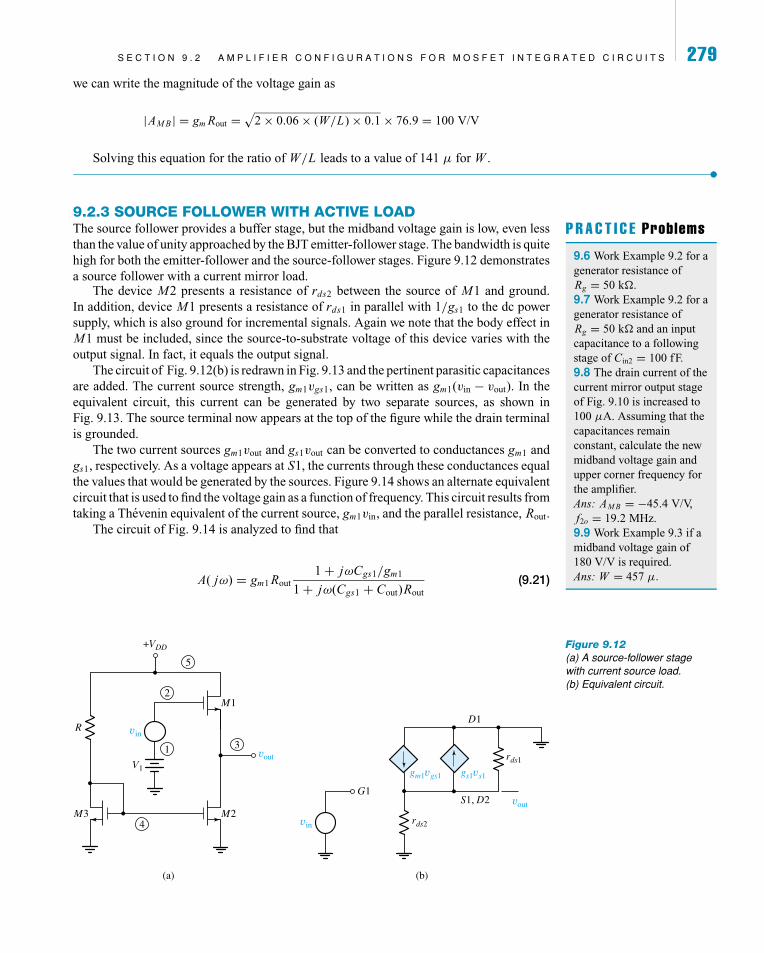
9.2.3 SOURCE FOLLOWER WITH ACTIVE LOADThe source follower provides a buffer stage, but the midband voltage gain is low, even lessthan the value of unity approached by the BJT emitter-follower stage. The bandwidth is quitehigh for both the emitter-follower and the source-follower stages. Figure 9.12 demonstratesa source follower with a current mirror load.
P R A C T I C E Problems
9.6 Work Example 9.2 for agenerator resistance ofRg = 50 k.9.7 Work Example 9.2 for agenerator resistance ofRg = 50 k and an inputcapacitance to a followingstage of Cin2 = 100 fF.9.8 The drain current of thecurrent mirror output stageof Fig. 9.10 is increased to100 µA. Assuming that thecapacitances remainconstant, calculate the newmidband voltage gain andupper corner frequency forthe amplifier.Ans: AM B = −45.4 V/V,f2o = 19.2 MHz.9.9 Work Example 9.3 if amidband voltage gain of180 V/V is required.Ans: W = 457 µ.
The device M2 presents a resistance of rds2 between the source of M1 and ground.In addition, device M1 presents a resistance of rds1 in parallel with 1/gs1 to the dc powersupply, which is also ground for incremental signals. Again we note that the body effect inM1 must be included, since the source-to-substrate voltage of this device varies with theoutput signal. In fact, it equals the output signal.
The circuit of Fig. 9.12(b) is redrawn in Fig. 9.13 and the pertinent parasitic capacitancesare added. The current source strength, gm1vgs1, can be written as gm1(vin − vout). In theequivalent circuit, this current can be generated by two separate sources, as shown inFig. 9.13. The source terminal now appears at the top of the figure while the drain terminalis grounded.
The two current sources gm1vout and gs1vout can be converted to conductances gm1 andgs1, respectively. As a voltage appears at S1, the currents through these conductances equalthe values that would be generated by the sources. Figure 9.14 shows an alternate equivalentcircuit that is used to find the voltage gain as a function of frequency. This circuit results fromtaking a Thevenin equivalent of the current source, gm1vin, and the parallel resistance, Rout.
The circuit of Fig. 9.14 is analyzed to find that
A( jω) = gm1 Rout1 + jωCgs1/gm1
1 + jω(Cgs1 + Cout)Rout(9.21)
+VDD
M3 M2
M1
G1
(b)(a)
D1
S1, D2
vin
vout
vout
V1
R
4
1
2
5
3
vin rds2
rds1
gm1vgs1 gs1vs1
Figure 9.12(a) A source-follower stagewith current source load.(b) Equivalent circuit.
P1: FCH/SPH P2: FCH/SPH QC: FCH/UKS T1: FCH
pb139B-09 ZP042-Sam.cls February 13, 2002 18:42
280 C H A P T E R 9 I N T E G R A T E D C I R C U I T D E S I G N W I T H T H E M O S F E T
(a)
Cgs1G1
D1
S1
vin voutgm1vin gm1vout gs1vout
rds1 rds2 Cout
(b)
Cgs1G1
D1
S1
vin voutgm1vin
rds2rds1 Coutgs1
1gm1
1Figure 9.13(a) The high-frequency sourcefollower equivalent circuit.(b) Using transconductancesfor two current sources.
where
Rout = 1
gm1 + gs1 + gds1 + gds2(9.22)
and
Cout = Csb1 + Cdb2 + Cgd2 ≈ Csb1 + Cdb2 (9.23)
The midband gain can be evaluated from Eqs. (9.21) and (9.22) to be
AM B = gm1
gm1 + gs1 + gds1 + gds2(9.24)
In many submicron processes, the value of the denominator of Eq. (9.24) might equal1.15 to 1.2 times gm1. This leads to values of midband gain ranging from about 0.8 to0.9 V/V.
The transfer function for voltage gain as a function of frequency shows a zero at
fzero = gm1
2πCgs1(9.25)
and a pole at
fpole = gm1 + gs1 + gds1 + gds2
2π (Cgs1 + Cout)(9.26)
Typically, the zero frequency is higher than the pole frequency, and the asymptoticfrequency response appears as in Fig. 9.15. At high frequencies the capacitor Cgs1 feeds
S E C T I O N 9 . 2 A M P L I F I E R C O N F I G U R A T I O N S F O R M O S F E T I N T E G R A T E D C I R C U I T S 281
fpole fzero
0 dB
f
AvdB
AhighdBFigure 9.15Asymptotic frequency responseof source follower.
through from input directly to output, causing a gain of
Ahigh = Cgs1
Cgs1 + Cout(9.27)
As we consider the large-signal operation of the source follower, we see that the outputvoltage can be driven positive to a value of VDD − Veff1 − VT 1. The negative voltage canreach Veff2 before M2 leaves the active region. The headroom is then VT 1 + Veff 1 + Veff 2.
E X A M P L E 9.4
In the source follower and current mirror of Fig. 9.12, a dc drain current of 50 µA passesthrough M1 and M2. The following parameters apply to the devices of the circuit at this biaspoint: gm1 = 199 µA/V, gs1 = 44 µA/V, gds1 = 1 µA/V, gds2 = 1.6 µA/V, Cgs1 = 7.1 fF,Csb1 = 12.6 fF, Cdb2 = 12.7 fF, and Cgd2 = 1.5 fF. Calculate the midband voltage gain,the pole frequency or upper corner frequency, and the zero frequency. Also calculatethe high frequency gain due to capacitor feedthrough of Cgs1. Simulate this circuit withSpice.
SOLUTION The midband voltage gain is calculated from Eq. (9.24) as
AM B = gm1
gm1 + gs1 + gds1 + gds2= 199
245.6= 0.810 V/V
The pole frequency that will be near the upper corner frequency is found from Eq. (9.26)to be
fpole = gm1 + gs1 + gds1 + gds2
2π (Cgs1 + Cout)= 245.6 × 10⁻⁶
2π × 33.9 × 10−15= 1.15 GHz
From Eq. (9.25), the zero frequency is calculated to be
fzero = gm1
2πCgs1= 199 × 10−6
2π × 7.1 × 10−15= 4.46 GHz
The high-frequency gain is
Ahigh = Cgs1
Cgs1 + Cout= 7.1
33.9= 0.209 V/V
The Spice simulation file is listed in Table 9.6.The frequency response resulting from this simulation is shown in Fig. 9.16. The simu-
lated midband gain is 0.811 V/V, which is very close to the calculated value of 0.810 V/V.The upper corner frequency from the simulation is 1.01 GHz, compared to a calculatedvalue of 1.15 GHz. The simulated zero frequency is 6.15 GHz, and the calculated valueis 4.46 MHz. The high-frequency gain had a simulated value of 0.16 V/V, whereas thecalculated value was 0.21 V/V.
P1: FCH/SPH P2: FCH/SPH QC: FCH/UKS T1: FCH
pb139B-09 ZP042-Sam.cls February 13, 2002 18:42
282 C H A P T E R 9 I N T E G R A T E D C I R C U I T D E S I G N W I T H T H E M O S F E T
A dc scan on the input voltage shows an output active region extending from approx-imately 0.32 to 3.03 V. The lower voltage is approximately Veff 2, and the upper voltageshould approximate VDD − Veff 1 − VT 1.
1.15 6.15f, GHz
AvdB
A = 0.811 V/V
Ahigh = 0.16 V/V
Figure 9.16Simulated frequency responsefor source follower.
We note that the upper corner frequency for the source follower is 1.01 GHz, compared to8.53 MHz for the comparable-sized current source load stage of Example 9.2. The primaryreason for this is the difference in the output resistance of the two stages. For the currentsource load stage, the output resistance is 339 k, and the source follower output resistanceis about 4 k. In order to compare this stage when driven by a signal generator resistance,a 339-k resistance is inserted in the input lead. This simulation leads to an overall uppercorner frequency of 101.5 MHz. The corresponding value for the current source load ofExample 9.2 is 3.08 MHz.
With a capacitive load of 1 pF and a generator resistance of 339 k, a Spice simulationshows an upper corner frequency of 37 MHz. Although this value is much lower than theunloaded value, it is considerably more than the corresponding frequency of the currentsource load stage, which was 399 kHz. Table 9.7 summarizes these results.
P R A C T I C A L Considerations
As noted earlier, capacitive loading can be a serious problem for an output stagethat connects to an IC pin, which will connect to the input of another circuit. Becauseof the high output resistance of configurations such as the active load stage, a smallcapacitance of a pF or less will decrease the upper corner frequency significantly.
P1: FCH/SPH P2: FCH/SPH QC: FCH/UKS T1: FCH
pb139B-09 ZP042-Sam.cls February 13, 2002 18:42
S E C T I O N 9 . 2 A M P L I F I E R C O N F I G U R A T I O N S F O R M O S F E T I N T E G R A T E D C I R C U I T S 283Table 9.7 Summary of Simulation Results forSource Follower
AM Bsim = −0.811 V/V
CL, pF Rg, kΩ f2o−sim, MHz
0 0 1,0101 0 36.60 339 101.61 339 37.2
The source follower stage is often inserted between a high-gain stage and the outputpin of a chip to serve as a buffer stage. This buffer presents a rather low capacitanceto the preceding stage, since there is no Miller multiplication of Cgd and, as seenfrom the simulation, a 1-pF load capacitance can result in a reasonably high uppercorner frequency.
9.2.4 THE CASCODE CONNECTIONThe cascode connection has been used for many years in high-frequency BJT circuits. Ithas become more important in IC MOSFET design in recent years. We will discuss theMOSFET cascode circuit in this section. Figure 9.17(a) shows the basic cascode circuitwith a current source load.
P R A C T I C E Problems
9.10 For the sourcefollower of Fig. 9.12, derivethe output resistancelooking into the sourceterminal of M1.9.11 If gds1 and gds2 areconsidered negligible for thesource follower of Example9.4, what will the midbandvoltage gain be?Ans: 0.819 V/V.
The equivalent circuit for the upper device would include a current generator of valuegm2Vgs2. For this connection, vgs2 = −vs2; thus this current generator reverses the direc-tion of current flow and removes the negative sign to lead to the value of gm2vs2, shown inFig. 9.17(b).
The resistance rcs is the output resistance of the current source. For a simple source, thisvalue would be rds . For a Wilson mirror, it would be considerably larger. The equivalentcircuit can be converted to a Thevenin circuit, as shown in Fig. 9.18. The output voltage is
vout = −ircs
where i is the incremental drain current. Note that the upper voltage source is proportionalto the source voltage of M2, vs2. This voltage can be expressed as
vs2 = −gm1rds1vin + irds1
ID
M2V
(a)
M1
vout
vin
G1
(b)
D2
D1, S2
S1
vout
vin
gm2vs2
gm1vin
gs2vs2
rds2
rds1
rcs
vs2—
Figure 9.17(a) The MOSFET cascodeamplifier stage. (b) Theequivalent circuit.
P1: FCH/SPH P2: FCH/SPH QC: FCH/UKS T1: FCH
pb139B-09 ZP042-Sam.cls February 13, 2002 18:42
284 C H A P T E R 9 I N T E G R A T E D C I R C U I T D E S I G N W I T H T H E M O S F E T
ivout
S1
D1, S2
D2
G1
vin
+
—
+— (gm2 + gs2)rds2vs2
gm1rds1vin
vs2
rds2
rcs
Figure 9.18An alternate equivalent circuitfor the cascode.
If the transconductance of M2 is added to the body effect transconductance—that is,
gt2 = gm2 + gs2
the midband voltage gain can be found to be
AM B = − (gm1rds1 + gt2gm1rds1rds2) rcs
rds1 + rds2 + rcs + gt2rds1rds2(9.28)
This expression represents the product of two relatively large gains. As bias currentdecreases, the rds terms increase faster than the gm terms decrease. Gains of several thousandcan be obtained with this circuit. However, as rds increases, the high-frequency responsedecreases, since the output resistance must drive the parasitic capacitance at the output ofthe stage.
A differential version of this stage is often used as an input stage in MOSFET op ampchips. A slightly different version of the cascode is the folded cascode that replaces M2 bya pMOS device with a drain connection to ground. We will not consider the folded cascodestage.
The headroom of the cascode circuit can be found to be
Vheadroom = Veff 1 + Veff 2 − Veff 3 (9.29)
The value of Veff 3 will be negative for the pMOS device of a simple current mirror.The upper corner frequency of the cascode can be found from the equivalent circuit,
shown in Fig. 9.19. The analysis of this circuit is somewhat complex. An accurate value ofthe upper corner frequency can be found by simulation, but it can be approximated rathereasily from the equivalent circuit. We first note that with no signal generator resistance, theinput capacitance will not influence the bandwidth. We next note that the corner frequencydue to the capacitance C1 will be affected by the parallel combination of rds1 and theimpedance looking into the source of M2. This impedance will be much less than rds1 andcan be approximated by
RS 2 = 1
gm2 + gs2
vin Cin
G1 D2
D1, S2
S1
gm1vin rds1
C1 C2+
—
+—
rds1 rds2vs2
(gm2 + gs2)vs2rds2rcs = rds3
vout
Figure 9.19High-frequency model of thecascode.
P1: FCH/SPH P2: FCH/SPH QC: FCH/UKS T1: FCH
pb139B-09 ZP042-Sam.cls February 13, 2002 18:42
S E C T I O N 9 . 2 A M P L I F I E R C O N F I G U R A T I O N S F O R M O S F E T I N T E G R A T E D C I R C U I T S 285This corner frequency will be quite large, at least compared to that caused by C2. If
the current source is a simple current mirror, its output impedance will be rcs = rds3. Theresistance seen by C2 is then rds3 ‖ Rout2, where Rout2 is the impedance looking into thedrain of M2. This latter impedance will be quite large since the source resistance of M2equals rds1. This source resistance increases the output resistance of M2 significantly; thus,the resistance seen by C2 is approximately rds3. The upper corner frequency of the cascodecan then be approximated by
f2o ≈ 1
2πrds3C2(9.30)
where C2 = Cdb2 + Cgd2 + Cdb3 + Cgd3.
E X A M P L E 9.5
The cascode circuit of Fig. 9.20 has a dc drain current for all transistors of 50 µA. Thiscurrent is supplied by a simple current mirror with M3 as the output device. With the biasvoltages shown, the parameters are gm1 = 181 µA/V, gm2 = 195 µA/V, gds1 = 5.87 µA/V,gs2 = 57.1 µA/V, gds2 = 0.939 µA/V, gds3 = 3.76 µA/V, Cdb2 = 9.8 fF, Cgd2 = 1.5 fF,Cdb3 = 40.9 fF, and Cgd3 = 4.5 fF, Calculate the midband voltage gain and the approximateupper corner frequency of this cascode stage. Verify these results with a Spice simulation.
SOLUTION The midband gain is calculated from Eq. (9.28).
AM B = − (gm1rds1 + gt2gm1rds1rds2) rds3
rds1 + rds2 + rds3 + gt2rds1rds2= −46.8 V/V
We note that this gain can be approximated by
AM B = −gm1rds3 = − 181
3.76= −48.1 V/V
Which assumes that the incremental current generated by device M1, gm1vin, flows throughM2 to develop the output voltage across rds3.
This low value of voltage gain could be increased sharply by increasing the outputimpedance of the current mirror to something much greater than rds3.
+5 V
M3 15/1
M2 5/1
M1 5/1
15/1 M4
vout
V1
72 kΩ
V2
V4
vin
2
4
1
6
7
5
3
Figure 9.20Cascode circuit for Example9.5.
P1: FCH/SPH P2: FCH/SPH QC: FCH/UKS T1: FCH
pb139B-09 ZP042-Sam.cls February 13, 2002 18:42
286 C H A P T E R 9 I N T E G R A T E D C I R C U I T D E S I G N W I T H T H E M O S F E T
The upper corner frequency is approximated by Eq. (9.30) as
The results of the simulation are AM Bsim = −46.9 V/V and f2o−sim = 9.65 MHz. Thecalculated gain is very close to the simulated value, and the upper corner frequency iscalculated to be about 10% higher than the simulated value.
In order to demonstrate the effect of current on gain and bandwidth, the dc drain currentof the circuit is dropped from 50 µA to 10.7 µA. For this situation, the simulated resultsare AM Bsim = −94.1 V/V and f2o−sim = 2.52 MHz. The gain has approximately doubled,while the bandwidth has dropped by a factor of about 4.
The effect on voltage gain can be seen from the approximation
AM B = −gm1rds3
Since gm varies as the square root of drain current and rds varies approximately inverselywith current, the voltage gain at a new current, ID2, compares to the voltage gain at a currentof ID1 as
AM B(ID2) =√
ID1
ID2AM B(ID1)
For this circuit, the new gain at 10.7 µA would be approximated as
AM B(10.7) =√
50
10.7AM B(50) = 2.16 × (−46.8) = −101 V/V
The bandwidth decrease is due to the increase in output resistance when drain current islowered.
P1: FCH/SPH P2: FCH/SPH QC: FCH/UKS T1: FCH
pb139B-09 ZP042-Sam.cls February 13, 2002 18:42
S E C T I O N 9 . 2 A M P L I F I E R C O N F I G U R A T I O N S F O R M O S F E T I N T E G R A T E D C I R C U I T S 287Table 9.9 Summary of Simulation Results forCascode Amplifier
AM Bsim = −46.9 V/V
CL, pF Rg, kΩ f2o−sim, MHz
0 0 9.651 0 0.550 339 8.951 339 0.55
If a signal generator resistance is present, a second corner frequency is added at the inputdue to Cin of Fig. 9.19. When a 339-k generator resistance is added to the simulation ofTable 9.8, the new upper corner frequency is 8.95 MHz. This value represents a relativelysmall change from the original value of 9.65 MHz, which implies that Cin is rather small.Thus we see one of the advantages of the cascode connection; that is, the input capacitanceis small because the Miller effect is minimized by a small voltage gain from gate to drainof M1.
If a load capacitance of 1 pF is added but no generator resistance is present, the uppercorner frequency is lowered to 552 kHz. Adding the generator resistance to this circuit leadsto no further reduction of the upper corner frequency.
The headroom for the cascode circuit is simulated to be about 0.94 V. Using simulatedvalues of the effective voltages of Eq. (9.29) gives a calculated value of
Vheadroom = 0.47 + 0.45 + 0.41 = 1.33 V
These results are summarized in Table 9.9.
P R A C T I C E Problem
9.12 Rework Example 9.5if the current from themirror is changed to 75 µA.
9.2.5 THE ACTIVE CASCODE AMPLIFIERAn amplifier that behaves much like the cascode circuit, but offers slightly more headroomand requires one less bias voltage source, is the active cascode stage of Fig. 9.21. It alsoexhibits high gain although it has a lower bandwidth than the cascode stage with a currentmirror load. The only difference between this circuit and the cascode circuit is that the gatesof both nMOS amplifying stages, M1 and M2, are tied together and driven by the inputsignal. The load is formed by the two pMOS devices, M3 and M4, which again connectboth gates together and also to a bias source. The connection of M3 and M4 is called apartial cascode stage.
VDD
VBB
VGG
M4
M3
M1
M2
vout
vin
Figure 9.21An active cascode stage witha partial cascode load.
The partial cascode can be found to present an output impedance, looking into the drainof M4, of
Ro4 = rds3 + rds4 + gt4rds3rds4 (9.31)
where gt4 = gm4 + gs4.The midband voltage gain is evaluated as
AM B = −(
gm1
gds1+ gm2
gds2+ gm1gt2
gds1gds2
Ro4
Ro4 + Ro2
)(9.32)
where
Ro2 = rds1 + rds2 + gt2rds3rds4 (9.33)
and gt2 = gm2 + gs2.
P1: FCH/SPH P2: FCH/SPH QC: FCH/UKS T1: FCH
pb139B-09 ZP042-Sam.cls February 13, 2002 18:42
288 C H A P T E R 9 I N T E G R A T E D C I R C U I T D E S I G N W I T H T H E M O S F E T
The device M2 is chosen to have a larger aspect ratio than that of M1, and the same istrue of M4 compared to M3. Thus the outer devices, M1 and M3, are forced to operate inthe triode region or near the edge of the triode and the active region.
The gain expression can be reduced by using aspect ratios of the pMOS devices that arethree times the corresponding nMOS devices, which will result in the following approximatetransconductance relationships:
gt2 = gt4 grds1 = grds3 gds2 = gds4
With some simple approximations, the voltage gain can be expressed as
AM B ≈ − gt2gm1
2gds1gds2(9.34)
The output impedance of the active cascode for comparable devices is considerablygreater than that of the cascode. Of course, additional devices could be used in the currentmirror load of the cascode to increase the output impedance. For a four-transistor circuit,the active cascode has higher gain, smaller headroom, and fewer required bias voltages. Thedisadvantage is a smaller bandwidth.
The headroom is
Vheadroom = Veff 1 + Veff 3 (9.35)
which may be 0.4 to 0.5 V.A Spice netlist file of the active cascode with drain currents equal to about 50 µA is
shown in Table 9.10.The results of this simulation are indicated in Table 9.11.Both the cascode and active cascode will show an increased gain and decreased band-
width as drain current decreases. For the circuits of Figs. 9.17(a) and 9.21, the drain currentsare decreased to approximately 10 µA. The new simulated results for the cascode circuitwith no additional loading are AM Bsim = −70.9 V/V and f2o−sim = 3.03 MHz. The resultsfor the active cascode are AM Bsim = −624 V/V and f2o−sim = 63 kHz.
All of the stages discussed in this chapter require a voltage bias on the gate of theamplifying stage. Voltage reference circuits can be constructed to provide the necessaryvoltage bias; however, these sources will not be considered here.
Table 9.10 Spice Netlist File for Active Cascode Amplifier
S E C T I O N 9 . 2 A M P L I F I E R C O N F I G U R A T I O N S F O R M O S F E T I N T E G R A T E D C I R C U I T S 289Table 9.11 Summary of Results for ActiveCascode Amplifier
AM Bsim = −291 V/V
CL, pF Rg, kΩ f2o−sim, kHz
0 0 2491 0 69.50 339 87.21 339 45.9
D I S C U S S I O N O F D E M O N S T R A T I O N P R O B L E M
The amplifier of the Demonstration Problem is repeated here for convenience. The first part ofthe problem consists of solving for the current through the 8-k resistance at the current mirrorinput, which will allow the output current from M2 to be equated to the current into M1 withan output voltage of 2.5 V.
5 V
8 kΩ
M2
M1
M3
vin
VDSQ1vout
V1
Amplifier for DemonstrationProblem
The drain current of M3 can be written as
ID3 = K p[VGS3 − VT p]2[1 − λ(VDS3 − VDS P3)]
We note that VGS3 = VG3 − VDD = 8ID3 − 5 V and VDS3 − VDS P3 = VT p = −1 V. Writing theright side of the drain current equation in terms of ID3 leads to a quadratic equation. The solutionof this equation results in ID3 = 0.2888 mA and VG3 = 2.31 V. The pinchoff current of bothM2 and M3 is
ID P = K p[VGS − VT p]2 = 0.1 × [−1.69]2 = 0.2856 mA
The pinchoff voltage is VDS P = −1.69 V.We now equate the current, ID2, to the current ID1, which allows the equation
When this voltage is applied to the gate of M1, a current of 0.2879 mA and a voltage ofVDSQ1 = 2.5V result.
The incremental values of rds1 and rds2 can now be found from
rds = 1
λIDS P
The values of rds1 and rds2 are equal and are both 350 k. The resistance between output andground is the parallel combination of these two resistances or 175 k.
The midband voltage gain is
AM B = −gm1 Rout
The value of gm is found to be
gm =√
2µCox(W/L)ID
For M1, the transconductance is 0.37 mA/V, which gives a gain of
AM B = −0.37 × 175 = −64.7 V/V
S U M M A R Y The MOSFET amplifier designed for implementation as
an IC reduces to a minimum the number of resistorsrequired. Active loads often replace the resistors used indiscrete MOSFET amplifiers.
The current mirror is used extensively in IC design. Itserves as a bias current source as well as an active load.
The individual amplifier stage must not be analyzed asan isolated stage. The driving source resistance that may
arise from a previous stage and the load capacitance thatmay arise from a following stage or an IC output padmust be included in the analysis of frequencyresponse.
The source follower has a low voltage gain but a very goodfrequency response.
The cascode and partial cascode connections provide ratherefficient amplifying configurations.
P1: FCH/SPH P2: FCH/SPH QC: FCH/UKS T1: FCH
pb139B-09 ZP042-Sam.cls February 13, 2002 18:42
P R O B L E M S 291
P R O B L E M SS E C T I O N 9 . 1 M O S F E T C U R R E N T M I R R O R S9.1 If µWCox/2L = 50 µA/V2, VT = 0.8 V, and λ = 0.02,
calculate the drain current in the circuit shown.
Figure P9.15 V
10 kΩ
9.2 For the circuit of Problem 9.1, calculate the value ofpinchoff current, ID P , and pinchoff voltage, VDS P .
9.3 If µWCox/2L = 80µA/V2, VT = −1.0 V, and λ = 0.02,calculate the drain current in the circuit shown.
Figure P9.35 V
8 kΩ
9.4 For the circuit of Problem 9.3, calculate the value of pin-choff current, ID P , and pinchoff voltage, VDS P .
9.5 If µWCox/2L = 50 µA/V2, VT = 0.8 V, and λ = 0.02,calculate the ratio Io/Iin for the circuit of Fig. 9.1
when Iin = 72 µA and VDS2 = 6 V. Assume matchedMOSFETs.
9.6 In Fig. 9.1, the current source, Iin, is generated by a 12-Vvoltage source in series with a 60-k resistor. Matcheddevices are used, except for VT 2, with values as given inProblem 9.5.
(a) Calculate the current, Iin.
(b) Calculate VGS .
(c) If Io/Iin is to be unity when VDS2 = 8 V, what is therequired value of VT 2?
(d) With the value of VT 2 in part (c), what is Io/Iin whenVDS2 = 16 V?
9.7 Derive the output impedance, looking into the drain, forthe circuit shown. Express the result in terms of rds , gm , andRS . Neglect body effect for this derivation. Compare thisimpedance to that resulting when RS = 0.
Figure P9.7
vout
+VDD
RS
V1
vin
Rout
S E C T I O N 9 . 2 . 1 S I M P L E A M P L I F I E R S T A G E S9.8 What is the approximate midband voltage gain for the
circuit of Fig. 9.4(a) if the dimensions of M1 are W1 = 24 µ
and L1 = 1 µ and the dimensions of M2 are W2 = 6 µ andL2 = 2 µ?
9.9 What should the value of W1 be in Fig. 9.4(a) to lead to amidband voltage gain of −42 V/V? The length of the channelof M1 is L1 = 1 µ, and the dimensions of M2 are W2 = 2 µ
and L2 = 2 µ.
D 9.10 If the circuit of Fig. 9.4(a) is to have a midband volt-age gain of approximately −4.8 V/V, to what value shouldW1 be changed?
9.11 What is the upper corner frequency of the amplifier ofFig. 9.4(a) if Cout = 98 fF, gm2 = 0.4 mA/V, and gs2 =0.05 mA/V? Assume that the load capacitance is50 fF.
S E C T I O N 9 . 2 . 2 A C T I V E L O A D S T A G E9.12 In the active load stage of Fig. 9.10, the current from the
mirror is increased from 50 µA to 100 µA. What would younow expect the midband voltage gain to be? Explain yourcalculations.
P1: FCH/SPH P2: FCH/SPH QC: FCH/UKS T1: FCH
pb139B-09 ZP042-Sam.cls February 13, 2002 18:42
292 C H A P T E R 9 I N T E G R A T E D C I R C U I T D E S I G N W I T H T H E M O S F E T
9.13 Rework the Demonstration Problem if all parame-ters remain the same except λp = 0.024 V−1 and λn =0.02 V−1.
9.14 Rework the Demonstration Problem if all parametersremain the same except Kn = 0.16 mA/V2.
9.15 In the circuit of Fig. 9.10, a resistance of value 400 k isplaced in series with the input signal generator. Calculate thevalue of load capacitance that causes the input upper cornerfrequency to equal the output upper corner frequency. Whatis the overall upper corner frequency? Use the capacitancevalues from the circuit simulation.
9.16 In the circuit of Fig. 9.10, a resistance is placed in se-ries with the input signal generator. Calculate the value ofthis resistor to cause the input upper corner frequency toequal the output upper corner frequency. Assume a zerovalue for load capacitance. Use the capacitance values fromthe circuit simulation. What is the overall upper cornerfrequency?
D 9.17 In the circuit shown, the current source has infi-nite impedance and can be adjusted to supply whatever cur-rent is required to keep M1 in the active region as VGS ischanged. If λ = 0.03 V−1, VT = 1.02 V, and µCoxW/2L =0.2 mA/V2,
(a) Calculate AM B when VGS = 2 V.
(b) Find the value of VGS required to double this voltagegain. Assume that VDS = 4 V for both cases.
Figure P9.17
vout
+VDD
VGS
vin
D 9.18 If the current source in Problem D9.17 is fixed at avalue of 100 µA, what must VGS be to result in VDS = 4 V?What is the value of AM B for this bias?
9.19 Rework Example 9.3 for a required midband voltage gainof −76 V/V.
9.20 In the circuit of Example 9.3, the drain current is loweredto 50 µA. Approximate the new value of midband voltagegain. Explain this approximation.
D 9.21 Using devices with L = 1 µ, |VT | = 1 V, λ = 0.02V−1, and µCox = 0.06 mA/V2, design an active load stagewith a simple current mirror load to have a midband gainof −120 V/V.
S E C T I O N 9 . 2 . 3 S O U R C E F O L L O W E R W I T H A C T I V E L O A D9.22 Rework Example 9.4 if all parameters remain the same
except gm , which becomes gm1 = 300 mA/V.
9.23 Find the overall upper corner frequency of the sourcefollower of Example 9.4 if a load capacitance of 0.6 pF isadded.
9.24 Find the overall upper corner frequency of the sourcefollower of Example 9.4 if a load capacitance of 0.6 pF isadded and a generator resistance of 100 k is present. Cal-culate the midband voltage gain.
S E C T I O N 9 . 2 . 4 T H E C A S C O D E C O N N E C T I O N9.25 In Example 9.5, using the cascode circuit of Fig. 9.20, the
current from the mirror is increased from 50 µA to 100 µA.What would you now expect the midband voltage gain tobe? Explain your calculations.
S E C T I O N 9 . 2 . 5 T H E A C T I V E C A S C O D E A M P L I F I E R9.26 Explain why the midband voltage gain increases with
decreasing drain current in the active cascode amplifier.