Integrated Dual RF Transmitter, Receiver, and Observation Receiver
Data Sheet ADRV9009
Rev. B Document Feedback Information furnished by Analog Devices is believed to be accurate and reliable. However, no responsibility is assumed by Analog Devices for its use, nor for any infringements of patents or other rights of third parties that may result from its use. Specifications subject to change without notice. No license is granted by implication or otherwise under any patent or patent rights of Analog Devices. Trademarks and registered trademarks are the property of their respective owners.
One Technology Way, P.O. Box 9106, Norwood, MA 02062-9106, U.S.A.Tel: 781.329.4700 ©2018–2019 Analog Devices, Inc. All rights reserved. Technical Support www.analog.com
FEATURES Dual transmitters Dual receivers Dual input shared observation receiver Maximum receiver bandwidth: 200 MHz Maximum tunable transmitter synthesis bandwidth:
450 MHz Maximum observation receiver bandwidth: 450 MHz Fully integrated fractional-N RF synthesizers Fully integrated clock synthesizer Multichip phase synchronization for RF LO and baseband
clocks JESD204B datapath interface Tuning range (center frequency): 75 MHz to 6000 MHz
APPLICATIONS 3G, 4G, and 5G TDD macrocell base stations TDD active antenna systems Massive multiple input, multiple output (MIMO) Phased array radar Electronic warfare Military communications Portable test equipment
GENERAL DESCRIPTION The ADRV9009 is a highly integrated, radio frequency (RF), agile transceiver offering dual transmitters and receivers, integrated synthesizers, and digital signal processing functions. The IC delivers a versatile combination of high performance and low power consumption demanded by 3G, 4G, and 5G macro cell time division duplex (TDD) base station applications.
The receive path consists of two independent, wide bandwidth, direct conversion receivers with state-of-the-art dynamic range. The device also supports a wide bandwidth, time shared observation path receiver (ORx) for use in TDD applications. The complete receive subsystem includes automatic and manual attenuation control, dc offset correction, quadrature error correction (QEC), and digital filtering, thus eliminating the need for these functions in the digital baseband. Several auxiliary functions, such as analog-to-digital converters (ADCs), digital-to-analog converters (DACs), and general-purpose inputs/outputs (GPIOs) for the power amplifier (PA), and RF front-end control are also integrated.
In addition to automatic gain control (AGC), the ADRV9009 also features flexible external gain control modes, allowing significant flexibility in setting system level gain dynamically.
The received signals are digitized with a set of four high dynamic range, continuous time Σ-Δ ADCs that provide inherent antialiasing. The combination of the direct conversion architecture, which does not suffer from out of band image mixing, and the lack of aliasing, relaxes the requirements of the RF filters when compared to traditional intermediate frequency (IF) receivers.
The transmitters use an innovative direct conversion modulator that achieves high modulation accuracy with exceptionally low noise.
The observation receiver path consists of a wide bandwidth, direct conversion receiver with state-of-the-art dynamic range.
The fully integrated phase-locked loop (PLL) provides high performance, low power, fractional-N RF frequency synthesis for the transmitter (Tx) and receiver (Rx) signal paths. An additional synthesizer generates the clocks needed for the converters, digital circuits, and the serial interface. A multichip synchronization mechanism synchronizes the phase of the RF local oscillator (LO) and baseband clocks between multiple ADRV9009 chips. Precautions are taken to provide the isolation required in high performance base station applications. All voltage controlled oscillators (VCOs) and loop filter components are integrated.
The high speed JESD204B interface supports up to 12.288 Gbps lane rates, resulting in two lanes per transmitter and a single lane per receiver in the widest bandwidth mode. The interface also supports interleaved mode for lower bandwidths, thus reducing the total number of high speed data interface lanes to one. Both fixed and floating point data formats are supported. The floating point format allows internal AGC to be invisible to the demodulator device.
The core of the ADRV9009 can be powered directly from 1.3 V regulators and 1.8 V regulators, and is controlled via a standard 4-wire serial port. Comprehensive power-down modes are included to minimize power consumption in normal use. The ADRV9009 is packaged in a 12 mm × 12 mm, 196-ball chip scale ball grid array (CSP_BGA).
ADRV9009 Data Sheet
Rev. B | Page 2 of 127
TABLE OF CONTENTS Features .............................................................................................. 1
Applications ....................................................................................... 1
General Description ......................................................................... 1
Revision History ............................................................................... 2
Functional Block Diagram .............................................................. 4
Specifications ..................................................................................... 5
Current and Power Consumption Specifications ................... 14
Timing Diagrams ........................................................................ 15
Absolute Maximum Ratings .......................................................... 16
Reflow Profile .............................................................................. 16
Thermal Management ............................................................... 16
Thermal Resistance .................................................................... 16
ESD Caution ................................................................................ 16
Pin Configuration and Function Descriptions ........................... 17
Typical Performance Characteristics ........................................... 23
75 MHz to 525 MHz Band ........................................................ 23
650 MHz to 3000 MHz Band .................................................... 44
3400 MHz to 4800 MHz Band .................................................. 63
5100 MHz to 5900 MHz Band .................................................. 80
Transmitter Output Impedance ................................................ 95
Observation Receiver Input Impedance .................................. 95
Receiver Input Impedance......................................................... 96
Terminology .................................................................................... 97
Theory of Operation ...................................................................... 98
Transmitter .................................................................................. 98
Receiver........................................................................................ 98
Observation Receiver ................................................................. 98
Clock Input .................................................................................. 98
Synthesizers ................................................................................. 98
SPI ................................................................................................. 99
JTAG Boundary Scan ................................................................. 99
Power Supply Sequence ............................................................. 99
GPIO_x Pins ............................................................................... 99
Auxiliary Converters .................................................................. 99
JESD204B Data Interface .......................................................... 99
Applications Information ............................................................ 101
PCB Layout and Power Supply Recommendations ............. 101
PCB Material and Stackup Selection ..................................... 101
Fanout and Trace Space Guidelines ....................................... 103
Component Placement and Routing Guidelines ................. 104
RF and JESD204B Transmission Line Layout ...................... 110
Isolation Techniques Used on the ADRV9009-W/PCBZ ... 114
RF Port Interface Information ................................................ 116
Outline Dimensions ..................................................................... 127
Ordering Guide ........................................................................ 127
REVISION HISTORY 5/2019—Rev. A to Rev B. Replaced ADRV9009 Customer Card to ADRV9009-WPCBZ ..................................................... Throughout Changes to Features Section............................................................ 1 Changes to Figure 1 .......................................................................... 4 Changes to Specifications Section and Table 1 ............................. 5 Change to Figure 2 ......................................................................... 15 Changes to Table 3 and Thermal Resistance Section ................. 16 Changes to 75 MHz to 525 MHz Band Section, Figures and Captions ........................................................................................... 23 Deleted Figure 83 to Figure 85; Renumbered Sequentially ...... 34 Added Figure 78, Figure 79, and Figure 80; Renumbered Sequentially ..................................................................................... 35 Added Figure 90 .............................................................................. 37 Added Figure 125 to Figure 127 ................................................... 43 Changes to 650 MHz to 3000 MHz Band Section, Figures and Captions ........................................................................................... 44 Changes to 3400 MHz to 4800 MHz Band Section, Figures and Captions ........................................................................................... 63 Changes to 5100 MHz to 5900 MHz Band Section, Figures and Captions ........................................................................................... 80
Changes to Terminology Section ................................................. 97 Deleted Figure 432 ......................................................................... 98 Changes to Theory of Operation Section and Clock Input Section ................................................................................... 98 Changed Serial Peripheral Interface Section to SPI Section and AUX DAC_x Section to Auxiliary DAC x Section ......................... 99 Changes to Power Supply Sequence Section, GPIO_x Pins Section, Auxiliary DAC x Section, and JESD204B Data Interface Section ............................................................................. 99 Changes to Table 7 Title, Figure 430, and Figure 431................... 100 Changes to Overview Section, PCB Material and Stackup Selection Section, and Figure 432 Caption ............................... 101 Changes to Table 9 and Table 10 ................................................ 102 Changes to Fanout and Trace Space Guidelines Section ......... 103 Changes to Signals with Highest Routing Priority Section and Figure 434 ...................................................................................... 104 Change to Figure 435 Caption .................................................... 105 Changes to Signals with Second Routing Priority Section and Figure 436 ...................................................................................... 106 Changes to Figure 437 ................................................................. 107 Changes to Figure 438 ................................................................. 108
Data Sheet ADRV9009
Rev. B | Page 3 of 127
Changes to Signals with Lowest Routing Priority Section and Figure 439 .......................................................................................109 Changes to RF Routing Guidelines Section and Figure 440 Caption ........................................................................110 Change to Figure 441 Caption .....................................................111 Changes to Transmitter Balun DC Feed Supplies Section .............................................................................112 Changes to Stripline Transmission Lines vs. Microstrip Transmission Lines Section .........................................................113 Moved Figure 444 to Isolation Techniques Used on the ADRV9009-W/PCBZ Section .....................................................114 Moved Figure 446 ..........................................................................115 Changes to Isolation Between JESD204B Lines Section ..........115 Changes to RF Port Interface Information Section ..................116
Deleted RF Port Interface Overview Section ............................ 117 Changes to Figure 448 Caption ................................................... 117 Moved Table 11 .............................................................................. 120 Changes to Figure 456 Caption to Figure 459 Caption ................ 121 Changes to General Receiver Path Interface Section ............... 122 Changes to Figure 463 .................................................................. 124 Changes to Figure 464 and Figure 465 ....................................... 125 Deleted Endnote 1, Table 12 to Endnote 1, Table 15; Renumbered Sequentially, and Endnote 2, Table 16 and Endnote 2, Table 17 ....................................................................... 126 Changes to Table 15 ...................................................................... 126 6/2018—Revision A: Initial Version
ADRV9009 Data Sheet
Rev. B | Page 4 of 127
FUNCTIONAL BLOCK DIAGRAM
RX1_IN +RX1_IN –
RX2_IN +RX2_IN –
ORX1_IN +ORX1_IN –
ORX2_IN +ORX2_IN –
RF_EXT_LO_I/O+RF_EXT_LO_I/O–
TX1_OUT +TX1_OUT –
TX2_OUT +TX2_OUT –
Rx1Rx2
ORx2
LOSYNTH
LPF
LPF
LPF
GPIOS, AUXADCs, AND AUXDACs
GPIO_3P3_x GPIO_x AUXADC_0 THROUGH AUXADC_3
CLOCKGENERATION
SYNCINx±
SERDOUTx±
SERDINx±
SYNCOUTx±
SYSREF_IN±
GP_INTERRUPT
RXx_ENABLE
TXx_ENABLE
RESET
TEST
SCLKCS
SDO
SDIO
REF_CLK_IN +REF_CLK_IN –
DIGITALPROCESSING
DECIMATIONpFIRAGC
DC-OFFSETQECLOL
JESD204BCIF/RIF
LPF
DAC
DAC
ADC
ARMM3
ADC
ORx1
ADRV9009
1649
9-00
1
Tx1
Tx2
Figure 1.
Data Sheet ADRV9009
Rev. B | Page 5 of 127
SPECIFICATIONS Electrical characteristics at VDDA1P31 = 1.3 V, VDDD1P3_DIG = 1.3 V, VDDA1P8_TX = 1.8 V, junction temperature (TJ) = full operating temperature range. LO frequency (fLO) = 1800 MHz, unless otherwise noted. The specifications in Table 1 are not de-embedded. Refer to the Typical Performance Characteristics section for input and output circuit path loss. The device configuration profile for the 75 MHz to 525 MHz frequency range is as follows: receiver = 50 MHz bandwidth (inphase quadrature (IQ) rate = 61.44 MHz), transmitter = 50 MHz transmitter large signal bandwidth and 100 MHz transmitter synthesis bandwidth (IQ rate = 122.88 MHz), observation receiver = 100 MHz bandwidth (IQ rate = 122.88 MHz), JESD204B rate = 9.8304 GSPS, and device clock = 245.76 MHz. Unless otherwise specified, the device configuration for all other frequency ranges is as follows: receiver = 200 MHz bandwidth (IQ rate = 245.76 MHz), transmitter = 200 MHz transmitter large signal bandwidth and 450 MHz transmitter synthesis bandwidth (IQ rate = 491.52 MHz), observation receiver = 450 MHz bandwidth (IQ rate = 491.52 MHz), JESD204B rate = 9.8304 GSPS, and device clock = 245.76 MHz.
Table 1. Parameter Symbol Min Typ Max Unit Test Conditions/Comments TRANSMITTERS
Center Frequency 75 6000 MHz Transmitter Synthesis
Bandwidth 450 MHz
Transmitter Large Signal Bandwidth
200 MHz
Peak-to-Peak Gain Deviation
1.0 dB 450 MHz bandwidth, compensated by programmable finite impulse response (FIR) filter
Gain Slope ±0.1 dB Any 20 MHz bandwidth span, compensated by programmable FIR filter
Deviation from Linear Phase 1 Degrees 450 MHz bandwidth Transmitter Attenuation
Power Control Range 0 32 dB Signal-to-noise ratio (SNR) maintained
for attenuation between 0 dB and 20 dB Transmitter Attenuation
Power Control Resolution 0.05 dB
Transmitter Attenuation Integral Nonlinearity
INL 0.1 dB For any 4 dB step
Transmitter Attenuation Differential Nonlinearity
DNL 0.04 dB Monotonic
Transmitter Attenuation Serial Peripheral Interface 2 (SPI 2) Timing
See Figure 4
Time from CS Going High to Change in Transmitter Attenuation
tSCH 19.5 24 ns
Time Between Consecutive Microattenuation Steps
tACH 6.5 8.1 ns A large change in attenuation can be broken up into a series of smaller attenuation changes
Time Required to Reach Final Attenuation Value
tDCH 800 ns Time required to complete the change in attenuation from start attenuation to final attenuation value
Maximum Attenuation Overshoot During Transition
−1.0 +0.5 dB
Change in Attenuation per Microstep
0.5 dB
Maximum Attenuation Change when CS Goes High
32 dB
ADRV9009 Data Sheet
Rev. B | Page 6 of 127
Parameter Symbol Min Typ Max Unit Test Conditions/Comments Adjacent Channel Leakage
Ratio (ACLR) Long Term Evolution (LTE)
20 MHz LTE at −12 dBFS
−67 dB 75 MHz < f ≤ 2800 MHz −64 dB 2800 MHz < f ≤ 4800 MHz −60 dB 4800 MHz < f ≤ 6000 MHz
In Band Noise Floor 0 dB attenuation, in band noise falls 1 dB for each dB of attenuation for attenuation between 0 dB and 20 dB
−147 dBm/Hz 75 MHz < f ≤ 600 MHz −148 dBm/Hz 600 MHz < f ≤ 3000 MHz −149 dBm/Hz 3000 MHz < f ≤ 4800 MHz −150.5 dBm/Hz 4800 MHz < f ≤ 6000 MHz
Out of Band Noise Floor 0 dB attenuation, 3 × bandwidth/2 offset −147 dBm/Hz 75 MHz < f ≤ 600 MHz −153 dBm/Hz 600 MHz < f ≤ 3000 MHz −154 dBm/Hz 3000 MHz < f ≤ 4800 MHz −155.5 dBm/Hz 4800 MHz < f ≤ 6000 MHz
Interpolation Images −80 dBc Transmitter to Transmitter
Isolation 85 dB 75 MHz < f ≤ 600 MHz
75 dB 600 MHz < f ≤ 2800 MHz 70 dB 2800 MHz < f ≤ 4800 MHz 65 dB 4800 MHz < f ≤ 5700 MHz 56 dB 5700 MHz < f ≤ 6000 MHz
Image Rejection Within Large Signal
Bandwidth QEC active
70 dB 75 MHz < f ≤ 600 MHz 65 dB 600 MHz < f ≤ 4000 MHz 62 dB 4000 MHz < f ≤ 4800 MHz 60 dB 4800 MHz < f ≤ 6000 MHz
Beyond Large Signal Bandwidth
40 dB Assumes that distortion power density is 25 dB below desired power density
Maximum Output Power 0 dBFS, continuous wave (CW) tone into 50 Ω load, 0 dB transmitter attenuation
9 dBm 75 MHz < f ≤ 600 MHz 7 dBm 600 MHz < f ≤ 3000 MHz 6 dBm 3000 MHz < f ≤ 4800 MHz 4.5 dBm 4800 MHz < f ≤ 6000 MHz
Third-Order Output Intermodulation Intercept Point
OIP3 0 dB transmitter attenuation
29 dBm 75 MHz < f ≤ 600 MHz 27 dBm 600 MHz < f ≤ 4000 MHz 23 dBm 4000 MHz < f ≤ 6000 MHz
Carrier Leakage With LO leakage correction active, 0 dB attenuation, scales decibel for decibel with attenuation, measured in 1 MHz bandwidth, resolution bandwidth and video bandwidth = 100 kHz, rms detector, 100 trace average
Carrier Offset from LO −84 dBFS 75 MHz < f ≤ 600 MHz −82 dBFS 600 MHz < f ≤ 4800 MHz −80 dBFS 4800 MHz < f ≤ 6000 MHz
Carrier on LO −71 dBFS
Data Sheet ADRV9009
Rev. B | Page 7 of 127
Parameter Symbol Min Typ Max Unit Test Conditions/Comments Error Vector Magnitude
(Third Generation Partnership Project (3GPP) Test Signals)
EVM
75 MHz LO 0.5 % 300 kHz RF PLL loop bandwidth, test equipment phase noise performance limited
1900 MHz LO 0.7 % 50 kHz RF PLL loop bandwidth 3800 MHz LO 0.7 % 300 kHz RF PLL loop bandwidth 5900 MHz LO 1.1 % 300 kHz RF PLL loop bandwidth
Output Impedance ZOUT 50 Ω Differential (see Figure 427) OBSERVATION RECEIVER ORx
Center Frequency 75 6000 MHz Gain Range 30 dB Third-order input intermodulation
intercept point (IIP3) improves decibel for decibel for the first 18 dB of gain attenuation, QEC performance optimi-zed for 0 dB to 6 dB of attenuation only
Analog Gain Step 0.5 dB For attenuator steps from 0 dB to 6 dB Peak-to-Peak Gain
Deviation 1 dB 450 MHz bandwidth, compensated by
programmable FIR filter Gain Slope ±0.1 dB Any 20 MHz bandwidth span, compens-
ated by programmable FIR filter Deviation from Linear Phase 1 Degree
s 450 MHz RF bandwidth
Observation Receiver Bandwidth
450 MHz
Observation Receiver Alias Band Rejection
60 dB Due to digital filters
Maximum Useable Input Level
PHIGH 0 dB attenuation, increases decibel for decibel with attenuation, CW corresponds to −1 dBFS at ADC
−11 dBm 75 MHz < f ≤ 3000 MHz −9.5 dBm 3000 MHz < f ≤ 4800 MHz −8 dBm 4800 MHz < f ≤ 6000 MHz
Integrated Noise −58.5 dBFS 450 MHz integration bandwidth −57.5 dBFS 491.52 MHz integration bandwidth
Second-Order Input Intermodulation Intercept Point
IIP2 62 dBm Maximum observation receiver gain, (PHIGH − 14 dB) per tone (see the Terminology section), 75 MHz < f ≤ 600 MHz
62 dBm Maximum observation receiver gain, (PHIGH − 8 dB) per tone (see the Terminology section), 600 MHz < f ≤ 3000 MHz
Third-Order Input Intermodulation Intercept Point
IIP3
Narrow Band 4 dBm 75 MHz < f ≤ 300 MHz, test condition: (PHIGH − 14) dB per tone
11 dBm 300 MHz < f ≤ 600 MHz, (PHIGH − 14) dB per tone
Third-order intermodulation product (IM3) product < 130 MHz at baseband, (PHIGH − 8) dB per tone
12 dBm 600 MHz < f ≤ 3000 MHz 12 dBm 3000 MHz < f ≤ 4800 MHz 11 dBm 4800 MHz < f ≤ 6000 MHz
ADRV9009 Data Sheet
Rev. B | Page 8 of 127
Parameter Symbol Min Typ Max Unit Test Conditions/Comments Wide Band
7 dBm 600 MHz < f ≤ 3000 MHz 7 dBm 3000 MHz < f ≤ 4800 MHz 6 dBm 4800 MHz < f ≤ 6000 MHz
Third-Order Intermodulation Product
IM3 IM3 product < 130 MHz at baseband, two tones, each at (PHIGH − 12) dB
−70 dBc 600 MHz < f ≤ 3000 MHz −67 dBc 3000 MHz < f ≤ 4800 MHz −62 dBc 4800 MHz < f ≤ 6000 MHz
Fifth-Order Intermodulation Product (1800 MHz)
IM5 −80 dBc IM5 product < 50 MHz at baseband, two tones, each at (PHIGH − 12) dB, 600 MHz < f ≤ 6000 MHz
Seventh-Order Intermodulation Product (1800 MHz)
IM7 −80 dBc IM7 product < 50 MHz at baseband, two tones, each at (PHIGH − 12) dB, 600 MHz < f ≤ 6000 MHz
Spurious-Free Dynamic Range
SFDR 70 dB Non IMx related spurs, does not include HDx, (PHIGH − 9) dB input signal, 600 MHz < f ≤ 6000 MHz
Harmonic Distortion (PHIGH − 11) dB input signal Second-Order Harmonic
Distortion Product HD2 −80 dBc (PHIGH – 11) dB input signal 75 MHz < f ≤
600 MHz, (PHIGH – 9) dB input signal 600 MHz < f ≤ 6000 MHz, in band harmo-nic distortion falls within ±100 MHz
−80 dBc Out of band harmonic distortion falls within ±225 MHz
Third-Order Harmonic Distortion Product
HD3 −70 dBc In band harmonic distortion falls within ±100 MHz
−60 dBc Out of band harmonic distortion falls within ±225 MHz
Image Rejection QEC active Within Large Signal
Bandwidth 65 dB
Outside Large Signal Bandwidth
55 dB
Input Impedance 100 Ω Differential (see Figure 428) Isolation
Transmitter 1 (Tx1) to Observation Receiver 1 (ORx1) and Transmitter 2 (Tx2) to Observation Receiver 2 (ORx2)
100 dB 75 MHz < f ≤ 600 MHz
65 dB 600 MHz < f ≤ 5300 MHz 55 dB 5300 MHz < f ≤ 6000 MHz
Tx1 to ORx2 and Tx2 to ORx1
105 dB 75 MHz < f ≤ 600 MHz
65 dB 600 MHz < f ≤ 5300 MHz 55 dB 5300 MHz < f ≤ 6000 MHz RECEIVERS
Center Frequency 75 6000 MHz Gain Range 30 dB Analog Gain Step 0.5 dB Attenuator steps from 0 dB to 6 dB
1 dB Attenuator steps from 6 dB to 30 dB Bandwidth Ripple ±0.5 dB 200 MHz bandwidth, compensated by
programmable FIR filter ±0.2 dB Any 20 MHz bandwidth span, compens-
ated by programmable FIR filter
Data Sheet ADRV9009
Rev. B | Page 9 of 127
Parameter Symbol Min Typ Max Unit Test Conditions/Comments Receiver Bandwidth 200 MHz Receiver Alias Band
Rejection 80 dB Due to digital filters
Maximum Useable Input Level
PHIGH 0 dB attenuation, increases decibel for decibel with attenuation, CW = 1800 MHz, corresponds to −1 dBFS at ADC
−11 dBm 75 MHz < f ≤ 3000 MHz −10.2 dBm 3000 MHz < f ≤ 4800 MHz −9.5 dBm 4800 MHz < f ≤ 6000 MHz
Noise Figure NF 0 dB attenuation, at receiver port 11.5 dB 75 MHz < f ≤ 600 MHz 12 dB 600 MHz < f ≤ 3000 MHz 13 dB 3000 MHz < f ≤ 4800 MHz 15.2 dB 4800 MHz < f ≤ 6000 MHz
Ripple 1.8 dB At band edge maximum bandwidth mode
Third-Order Input Intermodulation Intercept Point
IIP3
Difference Product IIP3D 12 dBm 75 MHz < f ≤ 600 MHz, (PHIGH − 12) dB per tone, 600 MHz < f ≤ 6000 MHz, (PHIGH − 10) dB per tone, two tones near band edge
Sum Product IIP3S 12 dBm 75 MHz < f ≤ 600 MHz, (PHIGH − 12) dB per tone, 600 MHz < f ≤ 6000 MHz, (PHIGH − 10) dB per tone, two tones at bandwidth/6 offset from the LO
Third-Order Harmonic Distortion Product
HD3 75 MHz < f ≤ 600 MHz, (PHIGH − 6) dB, 600 MHz < f ≤ 6000 MHz, (PHIGH − 4) dB, CW tone at bandwidth/6 offset from the LO
−65 dBc 75 MHz < f ≤ 600 MHz −66 dBc 600 MHz < f ≤ 4800 MHz −62 dBc 4800 MHz < f ≤ 6000 MHz
Second-Order Input Intermodulation Intercept Point
IIP2 62 dBm 75 MHz < f ≤ 600 MHz, (PHIGH − 12) dB per tone, 600 MHz < f ≤ 6000 MHz, (PHIGH − 10) dB per tone, 0 dB attenuation, complex
Image Rejection 75 dB QEC active, within 200 MHz receiver bandwidth
Input Impedance 100 Ω Differential (see Figure 429) Receiver to Receiver
Isolation 77 dB 75 MHz < f ≤ 600 MHz
65 dB 600 MHz < f ≤ 4800 MHz 61 dB 4800 MHz < f ≤ 6000 MHz
Receiver Band Spurs Referenced to RF Input at Maximum Gain
−95 dBm No more than one spur at this level per 10 MHz of receiver bandwidth
Receiver LO Leakage at Receiver Input at Maximum Gain
Leakage decreases decibel for decibel with attenuation for first 12 dB
−70 dBm 75 MHz < f ≤ 600 MHz −70 dBm 600 MHz < f ≤ 3000 MHz −65 dBm 3000 MHz < f ≤ 6000 MHz
ADRV9009 Data Sheet
Rev. B | Page 10 of 127
Parameter Symbol Min Typ Max Unit Test Conditions/Comments LO SYNTHESIZER
LO Frequency Step 2.3 Hz 1.5 GHz to 2.8 GHz, 76.8 MHz phase frequency detector (PFD) frequency
LO Spur −85 dBc Excludes integer boundary spurs Integrated Phase Noise 2 kHz to 18 MHz
75 MHz LO 0.014 °rms Narrow PLL loop bandwidth (50 kHz) 1900 MHz LO 0.2 °rms Narrow PLL loop bandwidth (50 kHz) 3800 MHz LO 0.36 °rms Wide PLL loop bandwidth (300 kHz) 5900 MHz LO 0.54 °rms Wide PLL loop bandwidth (300 kHz)
Spot Phase Noise 75 MHz LO Narrow PLL loop bandwidth
10 kHz Offset −126.5 dBc/Hz 100 kHz Offset −132.8 dBc/Hz 1 MHz Offset −150.1 dBc/Hz 10 MHz Offset −150.7 dBc/Hz
1900 MHz LO Narrow PLL loop bandwidth 100 kHz Offset −100 dBc/Hz 200 kHz Offset −115 dBc/Hz 400 kHz Offset −120 dBc/Hz 600 kHz Offset −129 dBc/Hz 800 kHz Offset −132 dBc/Hz 1.2 MHz Offset −135 dBc/Hz 1.8 MHz Offset −140 dBc/Hz 6 MHz Offset −150 dBc/Hz 10 MHz Offset −153 dBc/Hz
3800 MHz LO Wide PLL loop bandwidth 100 kHz Offset −104 dBc/Hz 1.2 MHz Offset −125 dBc/Hz 10 MHz Offset −145 dBc/Hz 5900 MHz LO Wide PLL loop bandwidth 100 kHz Offset −99 dBc/Hz 1.2 MHz Offset −119.7 dBc/Hz 10 MHz Offset −135.4 dBc/Hz
LO PHASE SYNCHRONIZATION Phase Deviation 1.6 ps/°C Change in LO delay per temperature
change EXTERNAL LO INPUT
Input Frequency fEXTLO 150 8000 MHz Input frequency must be 2 × the desired LO frequency
Input Signal Power 0 12 dBm 50 Ω matching at the source 3 dBm fEXTLO ≤ 2 GHz, add 0.5 dBm/GHz above
2 GHz 6 dBm fEXTLO = 8 GHz
External LO Input Signal Differential
To ensure adequate QEC
Phase Error 3.6 ps Amplitude Error 1 dB Duty Cycle Error 2 % Even Order Harmonics −50 dBc
CLOCK SYNTHESIZER Integrated Phase Noise 1 kHz to 100 MHz
1966.08 MHz LO 0.4 °rms PLL optimized for close in phase noise
Data Sheet ADRV9009
Rev. B | Page 11 of 127
Parameter Symbol Min Typ Max Unit Test Conditions/Comments Spot Phase Noise
1966.08 MHz 100 kHz Offset −109 dBc/Hz 1 MHz Offset −129 dBc/Hz 10 MHz Offset −149 dBc/Hz
REFERENCE CLOCK (REF_CLK_IN±)
Frequency Range 10 1000 MHz Signal Level 0.3 2.0 V p-p AC-coupled, common-mode voltage
(VCM) = 618 mV, for best spurious performance use <1 V p-p input clock
AUXILIARY CONVERTERS ADC
Resolution 12 Bits Input Voltage
Minimum 0.05 V Maximum VDDA_
3P3 − 0.05
V
DAC Resolution 10 Bits Includes four offset levels Output Voltage
Minimum 0.7 V 1 V voltage reference (VREF) Maximum VDDA_
3P3 − 0.3 V 2.5 V VREF
Output Drive Capability 10 mA DIGITAL SPECIFICATIONS
(COMPLEMENTARY METAL-OXIDE SEMICONDUCTOR (CMOS)) FOR SPI, GPIO_x, TXx_ENABLE, ORXx_ENABLE
Logic Inputs Input Voltage
High Level VDD_ INTERFACE × 0.8
VDD_ INTERFACE
V
Low Level 0 VDD_ INTERFACE × 0.2
V
Input Current High Level −10 +10 μA Low Level −10 +10 μA
Logic Outputs Output Voltage
High Level VDD_ INTERFACE × 0.8
V
Low Level VDD_ INTERFACE × 0.2
V
Drive Capability 3 mA
ADRV9009 Data Sheet
Rev. B | Page 12 of 127
Parameter Symbol Min Typ Max Unit Test Conditions/Comments DIGITAL SPECIFICATIONS
(CMOS) FOR GPIO_3P3_x
Logic Inputs Input Voltage
High Level VDDA_ 3P3 × 0.8
VDDA_3P3 V
Low Level 0 VDDA_ 3P3 × 0.2
V
Input Current High Level −10 +10 μA Low Level −10 +10 μA
Logic Outputs Output Voltage
High Level VDDA_ 3P3 × 0.8
V
Low Level VDDA_ 3P3 × 0.2
V
Drive Capability 4 mA DIGITAL SPECIFICATIONS
(LOW VOLTAGE DIFFERENTIAL SIGNALING (LVDS))
Logic Inputs (SYSREF_IN±, SYNCINx±)
Input Voltage Range 825 1675 mV Each differential input in the pair Input Differential
Voltage Threshold −100 +100 mV
Receiver Differential Input Impedance
100 Ω Internal termination enabled
Logic Outputs (SYNCOUTx±)
Output Voltage High 1375 mV Low 1025 mV
Output Differential Voltage
225 mV Programmable in 75 mV steps
Output Offset Voltage 1200 mV SPI TIMING
SCLK Period tCP 20 ns SCLK Pulse Width tMP 10 ns CS Setup to First SCLK Rising
Edge tSC 3 ns
Last SCLK Falling Edge to CS Hold
tHC 0 ns
SDIO Data Input Setup to SCLK
tS 2 ns
SDIO Data Input Hold to SCLK
tH 0 ns
SCLK Rising Edge to Output Data Delay (3-Wire or 4-Wire Mode)
tCO 3 8 ns
Bus Turnaround Time, Read After Baseband Processor (BBP) Drives Last Address Bit
tHZM tH tCO ns
Bus Turnaround Time, Read After ADRV9009 Drives Last Data Bit
tHZS 0 tCO ns
Data Sheet ADRV9009
Rev. B | Page 13 of 127
Parameter Symbol Min Typ Max Unit Test Conditions/Comments JESD204B DATA OUTPUT
TIMING AC-coupled
Unit Interval UI 81.38 320 ps Data Rate per Channel,
Nonreturn to Zero (NRZ) 3125 12,288 Mbps
Rise Time tR 24 39.5 ps 20% to 80% in 100 Ω load Fall Time tF 24 39.4 ps 20% to 80% in 100 Ω load Output Common-Mode
Voltage VCM 0 1.8 V AC-coupled
Differential Output Voltage VDIFF 360 600 770 mV Short-Circuit Current IDSHORT −100 +100 mA Differential Termination
Impedance 80 94.2 120 Ω
Total Jitter 15.13 ps Bit error rate (BER) = 10−15 Uncorrelated Bounded High
Probability Jitter UBHPJ 0.56 ps
Duty Cycle Distortion DCD 0.369 ps SYSREF_IN± Setup Time to
REF_CLK_IN± 2.5 ns See Figure 2
SYSREF_IN± Hold Time to REF_CLK_IN±
−1.5 ns See Figure 2
Latency tLAT_FRM REF_CLK_IN± = 245.76 MHz 116.5 Clock
cycles Observation receiver bandwidth = 450 MHz, IQ rate = 491.52 MHz, lane rate = 9830.4 MHz, number of converters (M) = 4, number of lanes (L) = 2, converter resolution (N) = 16, number of samples per converter (S) = 1
237.02 ns 89.4 Clock
cycles Receiver bandwidth = 200 MHz, IQ rate = 245.76 MHz, lane rate = 9830.4 MHz, M = 2, L = 2, N = 16, S = 1
364.18 ns JESD204B DATA INPUT TIMING AC-coupled
Unit Interval UI 81.38 320 ps Data Rate per Channel (NRZ) 3125 12288 Mbps Differential Voltage VDIFF 125 750 mV Termination Voltage (VTT)
Source Impedance ZTT 8.9 30 Ω
Differential Impedance ZRDIFF 80 105.1 120 Ω Termination Voltage VTT Ω
AC-Coupled 1.267 1.33 V Latency tLAT_DEFRM 74.45 Clock
cycles Device clock = 245.76 MHz, transmitter bandwidth = 200 MHz, IQ rate = 491.52 MHz, lane rate = 9830.4 MHz, M = 2, L = 2, N = 16, S = 1
153.5 ns 1 VDDA1P3 refers to all analog 1.3 V supplies, including: VDDA1P3_RF_SYNTH, VDDA1P3_BB, VDDA1P3_RX_RF, VDDA1P3_RX_TX, VDDA1P3_RF_VCO_LDO,
VDDA1P3_RF_LO, VDDA1P3_DES, VDDA1P3_SER, VDDA1P3_CLOCK_SYNTH, VDDA1P3_CLOCK_VCO_LDO, VDDA1P3_AUX_SYNTH, and VDDA1P3_AUX_VCO_LDO.
ADRV9009 Data Sheet
Rev. B | Page 14 of 127
CURRENT AND POWER CONSUMPTION SPECIFICATIONS
Table 2. Parameter Min Typ Max Unit Test Conditions/Comments SUPPLY CHARACTERISTICS
VDDA1P31 Analog Supply 1.267 1.3 1.33 V VDDD1P3_DIG Supply 1.267 1.3 1.33 V VDDA1P8_TX Supply 1.71 1.8 1.89 V VDDA1P8_BB Supply 1.71 1.8 1.89 V VDD_INTERFACE Supply 1.71 1.8 2.625 V CMOS and LVDS supply, 1.8 V to 2.5 V nominal range VDDA_3P3 Supply 3.135 3.3 3.465 V
POSITIVE SUPPLY CURRENT LO at 2600 MHz 450 MHz Transmitter Bandwidth,
Observation Receiver Disabled Two transmitters enabled
VDDA1P31 Analog Supply 1520 mA VDDD1P3_DIG Supply 619 mA Transmitter QEC active VDDA1P8_TX Supply 455 mA Transmitter RF attenuation = 0 dB, full-scale CW
135 mA Transmitter RF attenuation = 15 dB, full-scale CW VDDA1P8_BB Supply 30 mA VDD_INTERFACE Supply 8 mA VDD_INTERFACE = 2.5 V VDDA_3P3 Supply 3 mA No Auxiliary DAC x or AUXADC_x enabled, if enabled,
AUXADC_x adds 2.7 mA and each Auxiliary DAC x adds 1.5 mA Total Power Dissipation 3.68 W Typical supply voltages, 0 dB transmitter attenuation,
transmitter QEC active 3.11 W Typical supply voltages, 15 dB transmitter attenuation,
transmitter QEC active 450 MHz Transmitter Bandwidth,
Observation Receiver Enabled Two transmitters enabled, one ORx enabled
VDDA1P31 Analog Supply 2073 mA VDDD1P3_DIG Supply 1541 mA Transmitter QEC tracking active, observation receiver QEC
enabled, transmitter LTE20 centered on LO, observation receiver LTE20 at −16 dBm centered on LO
2100 mA Transmitter two tone = −99 MHz and 100 MHz at −7 dBFS each, observation receiver one tone = 100 MHz at −16 dBm
VDDA1P8_TX Supply 455 mA Transmitter RF attenuation = 0 dB, full scale CW 135 mA Transmitter RF attenuation = 15 dB, full scale CW
VDDA1P8_BB Supply 63 mA VDD_INTERFACE Supply 8 mA VDD_INTERFACE = 2.5 V VDDA_3P3 Power Supply 3 mA No Auxiliary DAC x or AUXADC_x enabled, if enabled,
AUXADC_x adds 2.7 mA and each Auxiliary DAC x adds 1.5 mA Total Power Dissipation 5.66 W Typical supply voltages, 0 dB transmitter attenuation,
transmitter QEC active 5.08 W Typical supply voltages, 15 dB transmitter attenuation,
transmitter QEC active 200 MHz Receiver Bandwidth,
Observation Receiver Disabled Two receivers enabled
VDDA1P31 Analog Supply 1645 mA VDDD1P3_DIG Supply 984 mA Receiver QEC active VDDA1P8_TX Supply 0.4 mA VDDA1P8_BB Supply 68 mA VDD_INTERFACE Supply 8 mA VDDA_3P3 Supply 3 mA No Auxiliary DAC x or AUXADC_x enabled, if enabled,
AUXADC_x adds 2.7 mA and each Auxiliary DAC x adds 1.5 mA Total Power Dissipation 3.57 W Typical supply voltages, receiver QEC active
1 VDDA1P3 refers to all analog 1.3 V supplies, including: VDDA1P3_RF_SYNTH, VDDA1P3_BB, VDDA1P3_RX_RF, VDDA1P3_RX_TX, VDDA1P3_RF_VCO_LDO, VDDA1P3_RF_LO, VDDA1P3_DES, VDDA1P3_SER, VDDA1P3_CLOCK_SYNTH, VDDA1P3_CLOCK_VCO_LDO, VDDA1P3_AUX_SYNTH, and VDDA1P3_AUX_VCO_LDO.
Data Sheet ADRV9009
Rev. B | Page 15 of 127
TIMING DIAGRAMS
REF_CLK_IN±
AT DEVICE PINS AT DEVICE COREREF_CLK_IN± DELAYIN REFERENCE TO SYSREF_IN±
CLK DELAY = 2nstH = –1.5nstS = +2.5ns
t’H = +0.5nst’S = +0.5ns
tS
tHtS
tH t’H
t’S t’S
t’H
1649
9-00
5
NOTES1. tH AND tS ARE THE HOLD AND SETUP TIMES FOR THE REF_CLK_IN± PINS. t’H AND t’S REFER TO THE DELAYED HOLD AND SETUP TIMES AT THE DEVICE CORE IN REFERENCE TO THE SYSREF_N± SIGNALS DUE TO AN INTERNAL BUFFER THAT THE SIGNAL PASSES THROUGH.
Figure 2. SYSREF_IN± Setup and Hold Timing
REF_CLK_IN±
SYSREF_IN±
VALID SYSREF INVALID SYSREFtH = –1.5nstS = +2.5ns
tS
tH
tS
tH
tS
tH
tS
tH
1649
9-00
6Figure 3. SYSREF_IN± Setup and Hold Timing Examples, Relative to Device Clock
tDCH
tSCH tACH
SCLK
SDIO
CS
TxATTENUATION
1649
9-00
7
Figure 4. Transmitter Attenuation Update via SPI 2 Port
ADRV9009 Data Sheet
Rev. B | Page 16 of 127
ABSOLUTE MAXIMUM RATINGS Table 3. Parameter Rating VDDA1P31 to VSSA −0.3 V to +1.4 V VDDD1P3_DIG to VSSD −0.3 V to +1.4 V VDD_INTERFACE to VSSA −0.3 V to +3.0 V VDDA_3P3 to VSSA −0.3 V to +3.9 V VDDA1P8_TX to VSSA −0.3 V to +2.0 V VDD_INTERFACE Logic Inputs and
Outputs to VSSD −0.3 V to VDD_ INTERFACE + 0.3 V
JESD204B Logic Outputs to VSSA −0.3 V to VDDA1P3_SER
JESD204B Logic Inputs to VSSA −0.3 V to VDDA1P3_DES +0.3 V
Input Current to any Pin Except Supplies
±10 mA
Maximum Input Power into RF Port 23 dBm (peak) Maximum Transmitter Voltage
Standing Wave Ratio (VSWR) 3:1
Maximum TJ 110°C Storage Temperature Range −65°C to +150°C
1 VDDA1P3 refers to all analog 1.3 V supplies.
Stresses at or above those listed under Absolute Maximum Ratings may cause permanent damage to the product. This is a stress rating only; functional operation of the product at these or any other conditions above those indicated in the operational section of this specification is not implied. Operation beyond the maximum operating conditions for extended periods may affect product reliability.
REFLOW PROFILE The ADRV9009 reflow profile is in accordance with the JEDEC JESD204B criteria for Pb-free devices. The maximum reflow temperature is 260°C.
THERMAL MANAGEMENT The ADRV9009 is a high power device that can dissipate over 3 W depending on the user application and configuration. Because of the power dissipation, the ADRV9009 uses an exposed die package to provide the customer with the most effective method of controlling the die temperature. The exposed die allows cooling of the die directly. Figure 5 shows the profile view of the device mounted to a user printed circuit board (PCB) and a heat sink (typically the aluminum case) to keep the junction (exposed die) below the maximum TJ detailed in Table 3. The device is designed for a lifetime of 10 years when operating at the maximum TJ.
THERMAL RESISTANCE Thermal performance is directly linked to PCB design and operating environment. Careful attention to PCB thermal design is required.
θJA is the natural convection junction to ambient thermal resistance measured in a circuit board for surface-mount packages.
θJC_TOP is the conduction thermal resistance from junction to case where the case temperature is measured at the top of the package.
Thermal resistance data for the ADRV9009 mounted on both a JEDEC 2S2P test board and a 10-layer Analog Devices, Inc., evaluation board is listed in Table 4. Do not exceed the absolute maximum TJ rating in Table 3. Ten-layer PCB entries refer to the 10-layer Analog Devices evaluation board, which more accurately reflects the PCB used in customer applications.
Table 4. Thermal Resistance1, 2 Package Type θJA θJC_TOP θJB ΨJT ΨJB Unit BC-196-13 21.1 0.04 4.9 0.3 4.9 °C/W
1 For the θJC test, 100 µm thermal interface material (TIM) is used. TIM is assumed to have 3.6 thermal conductivity watts/(meter × Kelvin).
2 Using enhanced heat removal techniques such as PCB, heat sink, and airflow improves the thermal resistance values.
ESD CAUTION
CUSTOMER CASE (HEAT SINK)
CUSTOMER THERMAL FILLER
SILICON (DIE)
PACKAGE SUBSTRATE
CUSTOMER PCB 1649
9-00
8
Figure 5. Typical Thermal Management Solution
Data Sheet ADRV9009
Rev. B | Page 17 of 127
PIN CONFIGURATION AND FUNCTION DESCRIPTIONS 1 2 3 4 5 6 7 8 9 10 11 12 13 14
A VSSA ORX2_IN+ ORX2_IN– VSSA RX2_IN+ RX2_IN– VSSA VSSA RX1_IN+ RX1_IN– VSSA ORX1_IN+ ORX1_IN– VSSA
BVDDA1P3_
RX_RF VSSA VSSA VSSA VSSA VSSARF_EXT_LO_I/O–
RF_EXT_LO_I/O+ VSSA VSSA VSSA VSSA VSSA VSSA
C GPIO_3P3_0 GPIO_3P3_3VDDA1P3_
RX_TX VSSAVDDA1P3_
RF_VCO_LDOVDDA1P3_
RF_VCO_LDOVDDA1P1_RF_VCO
VDDA1P3_RF_LO VSSA
VDDA1P3_AUX_VCO_
LDO VSSA VDDA_3P3 GPIO_3P3_9 RBIAS
D GPIO_3P3_1 GPIO_3P3_4 VSSA VSSA VSSA VSSA VSSA VSSA VSSAVDDA1P1_AUX_VCO VSSA VSSA GPIO_3P3_8 GPIO_3P3_10
E GPIO_3P3_2 GPIO_3P3_5 GPIO_3P3_6 VDDA1P8_BB VDDA1P3_BB VSSA REF_CLK_IN+ REF_CLK_IN– VSSAAUX_SYNTH_
OUT AUXADC_3 VDDA1P8_TX GPIO_3P3_7 GPIO_3P3_11
F VSSA VSSA AUXADC_0 AUXADC_1 VSSA VSSA VSSA VSSA VSSA VSSA AUXADC_2 VSSA VSSA VSSA
G VSSA VSSA VSSA VSSAVDDA1P3_
CLOCK_ SYNTH VSSAVDDA1P3_RF_SYNTH
VDDA1P3_AUX_SYNTH
RF_SYNTH_VTUNE VSSA VSSA VSSA VSSA VSSA
H TX2_OUT– VSSA VSSA VSSA VSSA VSSA VSSA VSSA VSSA VSSA GPIO_12 GPIO_11 VSSA TX1_OUT+
J TX2_OUT+ VSSA GPIO_18 RESETGP_
INTERRUPT TEST GPIO_2 GPIO_1 SDIO SDO GPIO_13 GPIO_10 VSSA TX1_OUT–
K VSSA VSSA SYSREF_IN+ SYSREF_IN– GPIO_5 GPIO_4 GPIO_3 GPIO_0 SCLK CS GPIO_14 GPIO_9 VSSA VSSA
L VSSA VSSA SYNCIN1– SYNCIN1+ GPIO_6 GPIO_7 VSSDVDDD1P3_
DIGVDDD1P3_
DIG VSSD GPIO_15 GPIO_8 SYNCOUT1– SYNCOUT1+
MVDDA1P1_
CLOCK_VCO VSSA SYNCIN0– SYNCIN0+ RX1_ENABLE TX1_ENABLE RX2_ENABLE TX2_ENABLE VSSA GPIO_17 GPIO_16VDD_
INTERFACE SYNCOUT0– SYNCOUT0+
NVDDA1P3_CLOCK_
VCO_LDO VSSA SERDOUT3– SERDOUT3+ SERDOUT2– SERDOUT2+ VSSAVDDA1P3_
SERVDDA1P3_
DES SERDIN1– SERDIN1+ SERDIN0– SERDIN0+ VSSA
PAUX_SYNTH_
VTUNE VSSA VSSA SERDOUT1– SERDOUT1+ SERDOUT0– SERDOUT0+VDDA1P3_
SERVDDA1P3_
DES VSSA SERDIN3– SERDIN3+ SERDIN2– SERDIN2+
ADRV900916499-900
Figure 6. Pin Configuration
Table 5. Pin Function Descriptions Pin No. Type Mnemonic Description A1, A4, A7, A8, A11, A14, B2 to
B6, B9 to B14, C4, C9, C11, D3 to D9, D11, D12, E6, E9, F1, F2, F5 to F10, F12 to F14, G1 to G4, G6, G10 to G14, H2 to H10, H13, J2, J13, K1, K2, K13, K14, L1, L2, M2, M9, N2, N7, N14, P2, P3, P10
Input VSSA Analog Supply Voltage (VSS).
A2, A3 Input ORX2_IN+, ORX2_IN− Differential Input for Observation Receiver 2. When unused, connect these pins to ground.
ADRV9009 Data Sheet
Rev. B | Page 18 of 127
Pin No. Type Mnemonic Description A5, A6 Input RX2_IN+, RX2_IN− Differential Input for Main Receiver 2. When unused, connect these pins
to ground. A9, A10 Input RX1_IN+, RX1_IN− Differential Input for Main Receiver 1. When unused, connect these
pins to ground. A12, A13 Input ORX1_IN+, ORX1_IN− Differential Input for Observation Receiver 1. When unused, connect
these pins to ground. B1 Input VDDA1P3_RX_RF Observation Receiver Supply. B7, B8 Input RF_EXT_LO_I/O−,
RF_EXT_LO_I/O+, Differential External LO Input/Output. If these pins are used for the external LO, the input frequency must be 2× the desired carrier frequency. When unused, do not connect these pins.
C1 Input/ output
GPIO_3P3_0 GPIO Pin Referenced to 3.3 V Supply. The alternate function is AUXDAC_4. Because this pin contains an input stage, the voltage on the pin must be controlled. When unused, this pin can be tied to ground through a resistor (to safeguard against misconfiguration), or this pin can be left floating, programmed as outputs, and driven low.
C2 Input/ output
GPIO_3P3_3 GPIO Pin Referenced to 3.3 V Supply. Because this pin contains an input stage, the voltage on the pin must be controlled. When unused, this pin can be tied to ground through a resistor (to safeguard against misconfiguration), or these pins can be left floating, programmed as outputs, and driven low.
C13 Input/ output
GPIO_3P3_9 GPIO Pin Referenced to 3.3 V Supply. The alternative function is AUXDAC_9. Because this pin contains an input stage, the voltage on the pin must be controlled. When unused, this pin can be tied to ground through a resistor (to safeguard against misconfiguration), or these pins can be left floating, programmed as outputs, and driven low.
D1 Input/ output
GPIO_3P3_1 GPIO Pin Referenced to 3.3 V Supply. The alternative function is AUXDAC_5. Because this pin contains an input stage, the voltage on the pin must be controlled. When unused, this pin can be tied to ground through a resistor (to safeguard against misconfiguration), or these pins can be left floating, programmed as outputs, and driven low.
D2 Input/ output
GPIO_3P3_4 GPIO Pin Referenced to 3.3 V Supply. The alternative function is AUXDAC_6. Because this pin contains an input stage, the voltage on the pin must be controlled. When unused, this pin can be tied to ground through a resistor (to safeguard against misconfiguration), or these pins can be left floating, programmed as outputs, and driven low.
D13 Input/ output
GPIO_3P3_8 GPIO Pin Referenced to 3.3 V Supply. The alternative function is AUXDAC_1. Because this pin contains an input stage, the voltage on the pin must be controlled. When unused, this pin can be tied to ground through a resistor (to safeguard against misconfiguration), or these pins can be left floating, programmed as outputs, and driven low.
D14 Input/ output
GPIO_3P3_10 GPIO Pin Referenced to 3.3 V Supply. The alternative function is AUXDAC_0. Because this pin contains an input stage, the voltage on the pin must be controlled. When unused, this pin can be tied to ground through a resistor (to safeguard against misconfiguration), or these pins can be left floating, programmed as outputs, and driven low.
E1 Input/ output
GPIO_3P3_2 GPIO Pin Referenced to 3.3 V Supply. Because this pin contains an input stage, the voltage on the pin must be controlled. When unused, this pin can be tied to ground through a resistor (to safeguard against misconfiguration), or these pins can be left floating, programmed as outputs, and driven low.
E2 Input/ output
GPIO_3P3_5 GPIO Pin Referenced to 3.3 V Supply. The alternative function is AUXDAC_7. Because this pin contains an input stage, the voltage on the pin must be controlled. When unused, this pin can be tied to ground through a resistor (to safeguard against misconfiguration), or these pins can be left floating, programmed as outputs, and driven low.
E3 Input/ output
GPIO_3P3_6 GPIO Pin Referenced to 3.3 V Supply. The alternative function is AUXDAC_8. Because this pin contains an input stage, the voltage on the pin must be controlled. When unused, this pin can be tied to ground through a resistor (to safeguard against misconfiguration), or these pins can be left floating, programmed as outputs, and driven low.
Data Sheet ADRV9009
Rev. B | Page 19 of 127
Pin No. Type Mnemonic Description E13 Input/
output GPIO_3P3_7 GPIO Pin Referenced to 3.3 V Supply. The alternative function is
AUXDAC_2. Because this pin contains an input stage, the voltage on the pin must be controlled. When unused, this pin can be tied to ground through a resistor (to safeguard against misconfiguration), or these pins can be left floating, programmed as outputs, and driven low.
E14 Input/ output
GPIO_3P3_11 GPIO Pin Referenced to 3.3 V Supply. The alternative function is AUXDAC_3. Because this pin contains an input stage, the voltage on the pin must be controlled. When unused, this pin can be tied to ground through a resistor (to safeguard against misconfiguration), or these pins can be left floating, programmed as outputs, and driven low.
C3 Input VDDA1P3_RX_TX 1.3 V Supply for Transmitter/Receiver Baseband Circuits, Transimpedance Amplifier (TIA), Transmitter Transconductance (GM), Baseband Filters, and Auxiliary DACs.
C5, C6 Input VDDA1P3_RF_VCO_LDO RF VCO LDO Supply Inputs. Connect Pin C5 to Pin C6. Use a separate trace on the PCB back to a common supply point.
C7 Input VDDA1P1_RF_VCO 1.1 V VCO Supply. Decouple this pin with 1 μF. C8 Input VDDA1P3_RF_LO 1.3 V LO Generator for the RF Synthesizer. This pin is sensitive to
supply noise. C10 Input VDDA1P3_AUX_VCO_LDO 1.3 V Supply. C12 Input VDDA_3P3 General-Purpose Output Pull-Up Voltage and Auxiliary DAC Supply
Voltage. C14 Input/
output RBIAS Bias Resistor. Tie this pin to ground using a 14.3 kΩ resistor. This pin
generates an internal current based on an external 1% resistor. D10 Input VDDA1P1_AUX_VCO 1.1 V VCO Supply. Decouple this pin with 1 μF. E4 Input VDDA1P8_BB 1.8 V Supply for the ADC and DAC. E5 Input VDDA1P3_BB 1.3 V Supply for the ADC, DAC, and AUXADC. E7, E8 Input REF_CLK_IN+,
REF_CLK_IN− Device Clock Differential Input.
E10 Output AUX_SYNTH_OUT Auxiliary PLL Output. When unused, do not connect this pin. E12 Input VDDA1P8_TX 1.8 V Supply for Transmitter. F3, F4, F11, E11 Input AUXADC_0 to AUXADC_3 Auxiliary ADC Input. When unused, connect these pins to ground with a
pull-down resistor, or connect directly to ground. G5 Input VDDA1P3_CLOCK_SYNTH 1.3 V Supply Input for Clock Synthesizer. Use a separate trace on the
PCB back to a common supply point. G7 Input VDDA1P3_RF_SYNTH 1.3 V RF Synthesizer Supply Input. This pin is sensitive to supply noise. G8 Input VDDA1P3_AUX_SYNTH 1.3 V Auxiliary Synthesizer Supply Input. G9 Output RF_SYNTH_VTUNE RF Synthesizer VTUNE Output. H11 Input/
output GPIO_12 Digital GPIO, 1.8 V to 2.5 V. Because this pin contains an input stage, the
voltage on the pin must be controlled. When unused, this pin can be tied to ground through a resistor (to safeguard against misconfiguration), or it can be left floating, programmed as output, and driven low.
H12 Input/ output
GPIO_11 Digital GPIO, 1.8 V to 2.5 V. Because this pin contains an input stage, the voltage on the pin must be controlled. When unused, this pin can be tied to ground through a resistor (to safeguard against misconfiguration), or it can be left floating, programmed as output, and driven low.
J11 Input/ output
GPIO_13 Digital GPIO, 1.8 V to 2.5 V. Because this pin contains an input stage, the voltage on the pin must be controlled. When unused, this pin can be tied to ground through a resistor (to safeguard against misconfiguration), or it can be left floating, programmed as output, and driven low.
J12 Input/ output
GPIO_10 Digital GPIO, 1.8 V to 2.5 V. Because this pin contains an input stage, the voltage on the pin must be controlled. When unused, this pin can be tied to ground through a resistor (to safeguard against misconfiguration), or it can be left floating, programmed as output, and driven low.
ADRV9009 Data Sheet
Rev. B | Page 20 of 127
Pin No. Type Mnemonic Description J3 Input/
output GPIO_18 Digital GPIO, 1.8 V to 2.5 V. The joint test action group (JTAG) function is
TCLK. Because this pin contains an input stage, the voltage on the pin must be controlled. When unused, this pin can be tied to ground through a resistor (to safeguard against misconfiguration), or it can be left floating, programmed as output, and driven low.
J7 Input/ output
GPIO_2 Digital GPIO, 1.8 V to 2.5 V. The user sets the JTAG function to 0. Because this pin contains an input stage, the voltage on the pin must be controlled. When unused, this pin can be tied to ground through a resistor (to safeguard against misconfiguration), or it can be left floating, programmed as output, and driven low.
J8 Input/ output
GPIO_1 Digital GPIO, 1.8 V to 2.5 V. The user sets the JTAG function to 0. Because this pin contains an input stage, the voltage on the pin must be controlled. When unused, this pin can be tied to ground through a resistor (to safeguard against misconfiguration), or it can be left floating, programmed as output, and driven low.
K5 Input/ output
GPIO_5 Digital GPIO, 1.8 V to 2.5 V. The JTAG function is TDO. Because this pin contains an input stage, the voltage on the pin must be controlled. When unused, this pin can be tied to ground through a resistor (to safeguard against misconfiguration), or it can be left floating, programmed as output, and driven low.
K6 Input/ output
GPIO_4 Digital GPIO, 1.8 V to 2.5 V. The JTAG function is TRST. Because this pin contains an input stage, the voltage on the pin must be controlled. When unused, this pin can be tied to ground through a resistor (to safeguard against misconfiguration), or it can be left floating, programmed as output, and driven low.
K7 Input/ output
GPIO_3 Digital GPIO, 1.8 V to 2.5 V. The user sets the JTAG function to 1. Because this pin contains an input stage, the voltage on the pin must be controlled. When unused, this pin can be tied to ground through a resistor (to safeguard against misconfiguration), or it can be left floating, programmed as output, and driven low.
K8 Input/ output
GPIO_0 Digital GPIO, 1.8 V to 2.5 V. The user sets the JTAG function to 1. Because this pin contains an input stage, the voltage on the pin must be controlled. When unused, this pin can be tied to ground through a resistor (to safeguard against misconfiguration), or it can be left floating, programmed as output, and driven low.
K11 Input/ output
GPIO_14 Digital GPIO, 1.8 V to 2.5 V. Because this pin contains an input stage, the voltage on the pin must be controlled. When unused, this pin can be tied to ground through a resistor (to safeguard against misconfiguration), or it can be left floating, programmed as output, and driven low.
K12 Input/ output
GPIO_9 Digital GPIO, 1.8 V to 2.5 V. Because this pin contains an input stage, the voltage on the pin must be controlled. When unused, this pin can be tied to ground through a resistor (to safeguard against misconfiguration), or it can be left floating, programmed as output, and driven low.
L5 Input/ output
GPIO_6 Digital GPIO, 1.8 V to 2.5 V. The JTAG function is TDI. Because this pin contains an input stage, the voltage on the pin must be controlled. When unused, this pin can be tied to ground through a resistor (to safeguard against misconfiguration), or it can be left floating, programmed as output, and driven low.
L6 Input/ output
GPIO_7 Digital GPIO, 1.8 V to 2.5 V. The JTAG function is TMS. Because this pin contains an input stage, the voltage on the pin must be controlled. When unused, this pin can be tied to ground through a resistor (to safeguard against misconfiguration), or it can be left floating, programmed as output, and driven low.
L11 Input/ output
GPIO_15 Digital GPIO, 1.8 V to 2.5 V. Because this pin contains an input stage, the voltage on the pin must be controlled. When unused, this pin can be tied to ground through a resistor (to safeguard against misconfiguration), or it can be left floating, programmed as output, and driven low.
Data Sheet ADRV9009
Rev. B | Page 21 of 127
Pin No. Type Mnemonic Description L12 Input/
output GPIO_8 Digital GPIO, 1.8 V to 2.5 V. Because this pin contains an input stage, the
voltage on the pin must be controlled. When unused, this pin can be tied to ground through a resistor (to safeguard against misconfiguration), or it can be left floating, programmed as output, and driven low.
M10 Input/ output
GPIO_17 Digital GPIO, 1.8 V to 2.5 V. Because this pin contains an input stage, the voltage on the pin must be controlled. When unused, this pin can be tied to ground through a resistor (to safeguard against misconfiguration), or it can be left floating, programmed as output, and driven low.
M11 Input/ output
GPIO_16 Digital GPIO, 1.8 V to 2.5 V. Because this pin contains an input stage, the voltage on the pin must be controlled. When unused, this pin can be tied to ground through a resistor (to safeguard against misconfiguration), or it can be left floating, programmed as output, and driven low.
H14, J14 Output TX1_OUT+, TX1_OUT− Transmitter 1 Output. When unused, do not connect these pins. H1, J1 Output TX2_OUT−, TX2_OUT+ Transmitter 2 Output. When unused, do not connect these pins. J4 Input RESET Active Low Chip Reset.
J5 Output GP_INTERRUPT General-Purpose Digital Interrupt Output Signal. When unused, do not connect this pin.
J6 Input TEST Pin Used for JTAG Boundary Scan. When unused, connect this pin to ground.
J9 Input/ output
SDIO Serial Data Input in 4-Wire Mode or Input/Output in 3-Wire Mode.
J10 Output SDO Serial Data Output. In SPI 3-wire mode, do not connect this pin. K3, K4 Input SYSREF_IN+, SYSREF_IN− LVDS Input. K9 Input SCLK Serial Data Bus Clock. K10 Input CS Serial Data Bus Chip Select, Active Low.
L3, L4 Input SYNCIN1−, SYNCIN1+ LVDS Input. These pins form the sync signal associated with receiver channel data on the JESD204B interface. When unused, connect these pins to ground with a pull-down resistor, or connect these pins directly to ground.
L7, L10 Input VSSD Digital VSS. L8, L9 Input VDDD1P3_DIG 1.3 V Digital Core. Connect Pin L8 and Pin L9 together. Use a wide
trace to connect to a separate power supply domain. L13, L14 Output SYNCOUT1−, SYNCOUT1+ LVDS Output. These pins form the sync signal associated with transmitter
channel data on the JESD204B interface. When unused, do not connect these pins.
M1 Input VDDA1P1_CLOCK_VCO 1.1 V VCO Supply. Decouple this pin with 1 μF. M3, M4 Input SYNCIN0−, SYNCIN0+ LVDS Input. These pins form the sync signal associated with receiver
channel data on the JESD204B interface. When unused, connect these pins to ground with a pull-down resistor, or connect these pins directly to ground.
M5 Input RX1_ENABLE Receiver 1 Enable Pin. When unused, connect this pin to ground with a pull-down resistor, or connect this pin directly to ground.
M6 Input TX1_ENABLE Transmitter 1 Enable Pin. When unused, connect this pin to ground with a pull-down resistor, or connect this pin directly to ground.
M7 Input RX2_ENABLE Receiver 2 Enable Pin. When unused, connect this pin to ground with a pull-down resistor, or connect this pin directly to ground.
M8 Input TX2_ENABLE Transmitter 2 Enable Pin. When unused, connect this pin to ground with a pull-down resistor, or connect this pin directly to ground.
M12 Input VDD_INTERFACE Input/Output Interface Supply, 1.8 V to 2.5 V. M13, M14 Output SYNCOUT0−, SYNCOUT0+ LVDS Output. These pins form the sync signal associated with transmitter
channel data on the JESD204B interface. When unused, do not connect these pins.
ADRV9009 Data Sheet
Rev. B | Page 22 of 127
Pin No. Type Mnemonic Description N1 Input VDDA1P3_CLOCK_
VCO_LDO 1.3 V Use Separate Trace to Common Supply Point.
N3, N4 Output SERDOUT3−, SERDOUT3+ RF Current Mode Logic (CML) Differential Output 3. When unused, do not connect these pins.
N5, N6 Output SERDOUT2−, SERDOUT2+ RF CML Differential Output 2. When unused, do not connect these pins. N8, P8 Input VDDA1P3_SER 1.3 V Supply for JESD204B Serializer. N9, P9 Input VDDA1P3_DES 1.3 V Supply for JESD204B Deserializer. N10, N11 Input SERDIN1−, SERDIN1+ RF CML Differential Input 1. When unused, do not connect these pins. N13, N12 Input SERDIN0+, SERDIN0− RF CML Differential Input 0. When unused, do not connect these pins. P1 Output AUX_SYNTH_VTUNE Auxiliary Synthesizer VTUNE Output. P4, P5 Output SERDOUT1−, SERDOUT1+, RF CML Differential Output 1. When unused, do not connect these
pins. P6, P7 Output SERDOUT0−,
SERDOUT0+, RF CML Differential Output 0. When unused, do not connect these pins.
P11, P12 Input SERDIN3−, SERDIN3+ RF CML Differential Input 3. When unused, do not connect these pins. P13, P14 Input SERDIN2−, SERDIN2+ RF CML Differential Input 2. When unused, do not connect these pins.
Data Sheet ADRV9009
Rev. B | Page 23 of 127
TYPICAL PERFORMANCE CHARACTERISTICS The temperature settings refer to the die temperature
75 MHz TO 525 MHz BAND 15
0
1
2
3
4
5
6
7
8
9
10
11
12
13
14
75 125 175 225 325275 375 425 475 525
TR
AN
SM
ITT
ER
CW
OU
TP
UT
PO
WE
R (
dB
m)
TRANSMITTER LO FREQUENCY (MHz)
Tx1 = +110°CTx1 = +25°CTx1 = –40°CTx2 = +110°CTx2 = +25°CTx2 = –40°C
16499-510
Figure 7. Transmitter CW Output Power vs. Transmitter LO Frequency, Transmitter QEC and External LO Leakage Active, Transmitter 50 MHz/100 MHz Bandwidth
Mode, IQ Rate = 122.88 MHz, Attenuation = 0 dB, Not De-Embedded
0
–100
–90
–80
–70
–60
–50
–40
–30
–20
–10
TR
AN
SM
ITT
ER
IM
AG
E R
EJE
CT
ION
(d
Bc)
+110°C ATTN = 20dB+110°C ATTN = 15dB+110°C ATTN = 10dB+110°C ATTN = 5dB+110°C ATTN = 0dB
+25°C ATTN = 20dB+25°C ATTN = 15dB+25°C ATTN = 10dB+25°C ATTN = 5dB+25°C ATTN = 0dB
–40°C ATTN = 20dB–40°C ATTN = 15dB–40°C ATTN = 10dB–40°C ATTN = 5dB–40°C ATTN = 0dB
–25 –20 –15 –10 –5 5 10 15 20 25
BASEBAND OFFSET FREQUENCY ANDTRANSMITTER ATTENUATION (MHz) 1
6499-511
Figure 8. Transmitter Image Rejection vs. Baseband Offset Frequency and Transmitter Attenuation, QEC Trained with Three Tones Placed at 10 MHz, 48 MHz, and 100 MHz (Tracking On), Total Combined Power = −10 dBFS,
Correction Then Frozen (Tracking Turned Off), CW Tone Swept Across Large Signal Bandwidth, LO = 75.2 MHz
0
–110
–100
–90
–80
–70
–60
–50
–40
–30
–20
–10
TR
AN
SM
ITT
ER
IM
AG
E R
EJE
CT
ION
(d
Bc)
+110°C ATTN = 20dB+110°C ATTN = 15dB+110°C ATTN = 10dB+110°C ATTN = 5dB+110°C ATTN = 0dB
+25°C ATTN = 20dB+25°C ATTN = 15dB+25°C ATTN = 10dB+25°C ATTN = 5dB+25°C ATTN = 0dB
–40°C ATTN = 20dB–40°C ATTN = 15dB–40°C ATTN = 10dB–40°C ATTN = 5dB–40°C ATTN = 0dB
–25 –20 –15 –10 –5 5 10 15 20 25BASEBAND OFFSET FREQUENCY AND
TRANSMITTER ATTENUATION FREQUENCY (MHz)
16499-512
Figure 9. Transmitter Image Rejection vs. Baseband Offset Frequency and Transmitter Attenuation, QEC Trained with Three Tones Placed at 10 MHz, 48 MHz, and 100 MHz (Tracking On), Total Combined Power = −10 dBFS,
Correction Then Frozen (Tracking Turned Off), CW Tone Swept Across Large Signal Bandwidth, LO = 300 MHz
0
–110
–90
–70
–50
–30
–10
–25 –20 –15 –10 –5 5 10 15 20 25
TR
AN
SM
ITT
ER
IM
AG
E R
EJE
CT
ION
(d
Bc)
BASEBAND OFFSET FREQUENCY ANDTRANSMITTER ATTENUATION (MHz)
+110°C ATTN = 20dB+110°C ATTN = 15dB+110°C ATTN = 10dB+110°C ATTN = 5dB+110°C ATTN = 0dB
+25°C ATTN = 20dB+25°C ATTN = 15dB+25°C ATTN = 10dB+25°C ATTN = 5dB+25°C ATTN = 0dB
–40°C ATTN = 20dB–40°C ATTN = 15dB–40°C ATTN = 10dB–40°C ATTN = 5dB–40°C ATTN = 0dB
16499-513
Figure 10. Transmitter Image Rejection vs. Baseband Offset Frequency and Transmitter Attenuation, QEC Trained with Three Tones Placed at 10 MHz, 48 MHz, and 100 MHz (Tracking On), Total Combined Power = −10 dBFS,
Correction Then Frozen (Tracking Turned Off), CW Tone Swept Across Large Signal Bandwidth, LO = 525 MHz
ADRV9009 Data Sheet
Rev. B | Page 24 of 127
0.5
–0.5
–0.4
–0.3
–0.2
–0.1
0.1
0
0.2
0.3
0.4
–50 –40 –30 –20 0–10 10 20 4030 50
TR
AN
SM
ITT
ER
PA
SS
BA
ND
FL
AT
NE
SS
(d
B)
BASEBAND OFFSET FREQUENCY (MHz)
Tx1 = +110°CTx1 = +25°CTx1 = –40°CTx2 = +110°CTx2 = +25°CTx2 = –40°C
16499-514
Figure 11. Transmitter Pass Band Flatness vs. Baseband Offset Frequency, Off Chip Match Response De-Embedded, LO = 300 MHz, Calibrated at 25°C
–75
–95
–93
–91
–89
–87
–85
–83
–81
–79
–77
75 125 175 225 325275 375 425 475 525
TR
AN
SM
ITT
ER
LO
LE
AK
AG
E (
dB
FS
)
TRANSMITTER LO FREQUENCY (MHz)
Tx1 = +110°CTx1 = +25°CTx1 = –40°CTx2 = +110°CTx2 = +25°CTx2 = –40°C
16499-515
Figure 12. Transmitter LO Leakage vs. Transmitter LO Frequency, Transmitter Attenuation = 0 dB, Baseband Tone Frequency = 10 MHz, Tracked
0
140
120
100
80
60
40
20
0 100 200 300 500400 600
TR
AN
SM
ITT
ER
TO
RE
CE
IVE
R I
SO
LA
TIO
N (
dB
)
RECEIVER LO FREQUENCY (MHz)
Tx1 – Rx1Tx1 – Rx2Tx2 – Rx1Tx2 – Rx2
16499-516
Figure 13. Transmitter to Receiver Isolation vs. Receiver LO Frequency, Temperature = 25°C
0
120
100
80
60
40
20
110
90
70
50
30
10
0 100 200 300 500400 600
TR
AN
SM
ITT
ER
TO
TR
AN
SM
ITT
ER
ISO
LA
TIO
N (
dB
)
TRANSMITTER LO FREQUENCY (MHz)
Tx1 – Tx2Tx2 – Tx1
16499-517
Figure 14. Transmitter to Transmitter Isolation vs. Transmitter LO Frequency, Temperature = 25°C
–140
–170
–160
–150
–165
–155
–145
0 1 2 3 54 6 7 8 109 11 12 13 1514 16 17 18 19 20
TR
AN
SM
ITT
ER
NO
ISE
(d
Bm
/Hz)
TRANSMITTER ATTENUATOR SETTING (dB)
525MHz = +110°C300MHz = +110°C75MHz = +110°C525MHz = +25°C300MHz = +25°C75MHz = +25°C525MHz = –40°C300MHz = –40°C75MHz = –40°C
16499-518
Figure 15. Transmitter Noise vs. Transmitter Attenuator Setting, Offset = 50 MHz
–40
–75
–65
–55
–70
–60
–50
–45
0 2 4 6 108 12 14 16 18 20
TR
AN
SM
ITT
ER
AD
JAC
EN
T C
HA
NN
EL
LE
AK
AG
E R
AT
IO (
dB
c)
TRANSMITTER ATTENUATOR SETTING (dB)
Tx1 +110°C (LOWER)Tx1 +110°C (UPPER)Tx1 +25°C (LOWER)Tx1 +25°C (UPPER)Tx1 –40°C (LOWER)Tx1 –40°C (UPPER)
Tx2 +110°C (LOWER)Tx2 +110°C (UPPER)Tx2 +25°C (LOWER)Tx2 +25°C (UPPER)Tx2 –40°C (LOWER)Tx2 –40°C (UPPER)
16499-519
Figure 16. Transmitter Adjacent Channel Leakage Ratio vs. Transmitter Attenuator Setting, Signal Offset = 0 MHz, LO = 75 MHz, LTE = 20 MHz, Peak to Average Ratio (PAR) = 12 dB, DAC Boost Normal, Upper Side and Lower Side, Performance Limited by Spectrum Analyzer at Higher Attenuation Settings
Data Sheet ADRV9009
Rev. B | Page 25 of 127
–40
–75
–65
–55
–70
–60
–50
–45
0 2 4 6 108 12 14 16 18 20
TR
AN
SM
ITT
ER
AD
JAC
EN
T C
HA
NN
EL
LE
AK
AG
E R
AT
IO (
dB
c)
TRANSMITTER ATTENUATOR SETTING (dB)
Tx1 +110°C (LOWER)Tx1 +110°C (UPPER)Tx1 +25°C (LOWER)Tx1 +25°C (UPPER)Tx1 –40°C (LOWER)Tx1 –40°C (UPPER)
Tx2 +110°C (LOWER)Tx2 +110°C (UPPER)Tx2 +25°C (LOWER)Tx2 +25°C (UPPER)Tx2 –40°C (LOWER)Tx2 –40°C (UPPER)
16499-520
Figure 17. Transmitter Adjacent Channel Leakage Ratio vs. Transmitter Attenuator Setting, Signal Offset = 0 MHz, LO = 300 MHz, LTE = 20 MHz,
PAR = 12 dB, DAC Boost Normal, Upper Side and Lower Side, Performance Limited by Spectrum Analyzer at Higher Attenuation Settings
–40
–75
–65
–55
–70
–60
–50
–45
0 2 4 6 108 12 14 16 18 20
TR
AN
SM
ITT
ER
AD
JAC
EN
T C
HA
NN
EL
LE
AK
AG
E R
AT
IO (
dB
c)
TRANSMITTER ATTENUATOR SETTING (dB)
Tx1 +110°C (LOWER)Tx1 +110°C (UPPER)Tx1 +25°C (LOWER)Tx1 +25°C (UPPER)Tx1 –40°C (LOWER)Tx1 –40°C (UPPER)
Tx2 +110°C (LOWER)Tx2 +110°C (UPPER)Tx2 +25°C (LOWER)Tx2 +25°C (UPPER)Tx2 –40°C (LOWER)Tx2 –40°C (UPPER)
16499-521
Figure 18. Transmitter Adjacent Channel Leakage Ratio vs. Transmitter Attenuator Setting, Signal Offset = 0 MHz, LO = 525 MHz, LTE = 20 MHz,
PAR = 12 dB, DAC Boost Normal, Upper Side and Lower Side, Performance Limited by Spectrum Analyzer at Higher Attenuation Settings
50
0
10
20
30
5
15
25
35
40
45
0 2 8 14 26204 10 16 28226 12 18 3024 32
TR
AN
SM
ITT
ER
OIP
3, R
IGH
T (
dB
m)
TRANSMITTER ATTENUATOR SETTING (dB)
+110°C+25°C–40°C
16499-522
Figure 19. Transmitter OIP3 Right vs. Transmitter Attenuator Setting, LO = 75 MHz, Total Root Mean Square (RMS) Power = −12 dBFS, 20 MHz/25 MHz Tones
50
0
10
20
30
5
15
25
35
40
45
0 2 8 14 26204 10 16 28226 12 18 3024 32
TR
AN
SM
ITT
ER
OIP
3, R
IGH
T (
dB
m)
TRANSMITTER ATTENUATOR SETTING (dB)
+110°C+25°C–40°C
16499-523
Figure 20. Transmitter OIP3 Right vs. Transmitter Attenuator Setting, LO = 300 MHz, Total RMS Power = −12 dBFS, 20 MHz/25 MHz Tones
50
0
10
20
30
5
15
25
35
40
45
0 2 8 14 26204 10 16 28226 12 18 3024 32
TR
AN
SM
ITT
ER
OIP
3, R
IGH
T (
dB
m)
TRANSMITTER ATTENUATOR SETTING (dB)
+110°C+25°C–40°C
16499-524
Figure 21. Transmitter OIP3 Right vs. Transmitter Attenuator Setting, LO = 525 MHz, Total RMS Power = −12 dBFS, 20 MHz/25 MHz Tones
50
0
10
20
30
5
15
25
35
40
45
1015
1520
510
2025
TR
AN
SM
ITT
ER
OIP
3, R
IGH
T (
dB
m)
BASEBAND TONE PAIR SWEPT ACROSS PASS BAND (MHz)
Tx1 = +110°CTx1 = +25°CTx1 = –40°CTx2 = +110°CTx2 = +25°CTx2 = –40°C
16499-525
Figure 22. Transmitter OIP3 Right vs. Baseband Tone Pair Swept Across Pass Band, LO = 75 MHz, Total RMS Power = −12 dBFS, Transmitter Attenuation = 4 dB
ADRV9009 Data Sheet
Rev. B | Page 26 of 127
50
0
10
20
30
5
15
25
35
40
45
1015
1520
510
2025
TR
AN
SM
ITT
ER
OIP
3, R
IGH
T (
dB
m)
BASEBAND FREQUENCY OFFSET (MHz)
Tx1 = +110°CTx1 = +25°CTx1 = –40°CTx2 = +110°CTx2 = +25°CTx2 = –40°C
16499-526
Figure 23. Transmitter OIP3 Right vs. Baseband Frequency Offset, LO = 300 MHz, Total RMS Power = −12 dBFS, Transmitter Attenuation = 4 dB
50
0
10
20
30
5
15
25
35
40
45
1015
1520
510
2025
TR
AN
SM
ITT
ER
OIP
3, R
IGH
T (
dB
m)
BASEBAND FREQUENCY OFFSET (MHz)
Tx1 = +110°CTx1 = +25°CTx1 = –40°CTx2 = +110°CTx2 = +25°CTx2 = –40°C
16499-527
Figure 24. Transmitter OIP3 Right vs. Baseband Frequency Offset, LO = 525 MHz, Total RMS Power = −12 dBFS, Transmitter Attenuation = 4 dB
0
–20
–120
–100
–80
–60
–40
0 4 8 12 2016 24 28 32
TR
AN
SM
ITT
ER
HD
2 (d
Bc)
TRANSMITTER ATTENUATOR SETTING (dB)
+110°C = (UPPER)+110°C = (HD2)+25°C = (UPPER)+25°C = (HD2)–40°C = (UPPER)–40°C = (HD2)
2 6 10 1814 22 26 30
16499-528
Figure 25. Transmitter HD2 vs. Transmitter Attenuator Setting, Baseband Frequency = 10 MHz, LO = 75 MHz, CW = −15 dBFS
0
–20
–120
–100
–80
–60
–40
0 4 8 12 2016 24 28 32
TR
AN
SM
ITT
ER
HD
2 (d
Bc)
TRANSMITTER ATTENUATOR SETTING (dB)
+110°C = (UPPER)+110°C = (HD2)+25°C = (UPPER)+25°C = (HD2)–40°C = (UPPER)–40°C = (HD2)
2 6 10 1814 22 26 30
16499-529
Figure 26. Transmitter HD2 vs. Transmitter Attenuator Setting, Baseband Frequency = 10 MHz, LO = 300 MHz, CW = −15 dBFS
0
–20
–120
–100
–80
–60
–40
0 4 8 12 2016 24 28 32
TR
AN
SM
ITT
ER
HD
2 (d
Bc)
TRANSMITTER ATTENUATOR SETTING (dB)
+110°C = (UPPER)+110°C = (HD2)+25°C = (UPPER)+25°C = (HD2)–40°C = (UPPER)–40°C = (HD2)
2 6 10 1814 22 26 30
16499-530
Figure 27. Transmitter HD2 vs. Transmitter Attenuator Setting, Baseband Frequency = 10 MHz, LO = 525 MHz, CW = −15 dBFS
0
–20
–100
–90
–80
–60
–40
–10
–70
–50
–30
0 4 8 12 2016 24 28 32
TR
AN
SM
ITT
ER
HD
3 (d
Bc)
TRANSMITTER ATTENUATOR SETTING (dB)
Tx1 = +110°CTx1 = +25°CTx1 = –40°CTx2 = +110°CTx2 = +25°CTx2 = –40°C
2 6 10 1814 22 26 30
16499-531
Figure 28. Transmitter HD3 vs. Transmitter Attenuator Setting, LO = 75 MHz, CW = −15 dBFS, Baseband Frequency = 10 MHz
Data Sheet ADRV9009
Rev. B | Page 27 of 127
0
–20
–120
–110
–100
–90
–80
–60
–40
–10
–70
–50
–30
0 4 8 12 2016 24 28 32
TR
AN
SM
ITT
ER
HD
3 (d
Bc)
TRANSMITTER ATTENUATOR SETTING (dB)
Tx1 = +110°CTx1 = +25°CTx1 = –40°CTx2 = +110°CTx2 = +25°CTx2 = –40°C
2 6 10 1814 22 26 30
16499-532
Figure 29. Transmitter HD3 vs. Transmitter Attenuator Setting, LO = 300 MHz, CW = −15 dBFS, Baseband Frequency = 10 MHz
0
–20
–120
–110
–100
–90
–80
–60
–40
–10
–70
–50
–30
0 4 8 12 2016 24 28 32
TR
AN
SM
ITT
ER
HD
3 (d
Bc)
TRANSMITTER ATTENUATOR SETTING (dB)
Tx1 = +110°CTx1 = +25°CTx1 = –40°CTx2 = +110°CTx2 = +25°CTx2 = –40°C
2 6 10 1814 22 26 30
16499-533
Figure 30. Transmitter HD3 vs. Transmitter Attenuator Setting, LO = 525 MHz, CW = −15 dBFS, Baseband Frequency = 10 MHz
0
–20
–120
–110
–100
–90
–80
–60
–40
–10
–70
–50
–30
0 4 8 12 2016 24 28 32
TR
AN
SM
ITT
ER
HD
3 IM
AG
E (
dB
c)A
PP
EA
RS
ON
SA
ME
SID
E A
S D
ES
IRE
D S
IGN
AL
TRANSMITTER ATTENUATOR SETTING (dB)
Tx1 = +110°CTx1 = +25°CTx1 = –40°CTx2 = +110°CTx2 = +25°CTx2 = –40°C
2 6 10 1814 22 26 30
16499-534
Figure 31. Transmitter HD3 Image Appears on Same Side as Desired Signal vs. Transmitter Attenuator Setting, LO = 75 MHz, CW = −15 dBFS
0
–20
–120
–110
–100
–90
–80
–60
–40
–10
–70
–50
–30
0 4 8 12 2016 24 28 32
TR
AN
SM
ITT
ER
HD
3 IM
AG
E (
dB
c)A
PP
EA
RS
ON
SA
ME
SID
E A
S D
ES
IRE
D S
IGN
AL
TRANSMITTER ATTENUATOR SETTING (dB)
Tx1 = +110°CTx1 = +25°CTx1 = –40°CTx2 = +110°CTx2 = +25°CTx2 = –40°C
2 6 10 1814 22 26 30
16499-535
Figure 32. Transmitter HD3 Image Appears on Same Side as Desired Signal vs. Transmitter Attenuator Setting, LO = 300 MHz, CW = −15 dBFS
0
–20
–130
–120
–110
–100
–90
–80
–60
–40
–10
–70
–50
–30
0 4 8 12 2016 24 28 32
TR
AN
SM
ITT
ER
HD
3 IM
AG
E (
dB
c)A
PP
EA
RS
ON
SA
ME
SID
E A
S D
ES
IRE
D S
IGN
AL
TRANSMITTER ATTENUATOR SETTING (dB)
Tx1 = +110°CTx1 = +25°CTx1 = –40°CTx2 = +110°CTx2 = +25°CTx2 = –40°C
2 6 10 1814 22 26 30
16499-536
Figure 33. Transmitter HD3 Image Appears on Same Side as Desired Signal vs. Transmitter Attenuator Setting, LO = 525 MHz, CW = −15 dBFS
0.03
–0.02
–0.01
0
0.01
0.02
TR
AN
SM
ITT
ER
AT
TE
NU
AT
OR
ST
EP
ER
RO
R (
dB
)
TRANSMITTER ATTENUATOR SETTING (dB)
0 4 8 12 2016 24 28 322 6 10 1814 22 26 30
+110°C+25°C–40°C
16499-537
Figure 34. Transmitter Attenuator Step Error vs. Transmitter Attenuator Setting, LO = 75 MHz, Baseband Frequency = 10 MHz, Backoff = 15 dBFS
ADRV9009 Data Sheet
Rev. B | Page 28 of 127
0.03
–0.02
–0.01
0
0.01
0.02
TR
AN
SM
ITT
ER
AT
TE
NU
AT
OR
ST
EP
ER
RO
R (
dB
)
TRANSMITTER ATTENUATOR SETTING (dB)
0 4 8 12 2016 24 28 322 6 10 1814 22 26 30
+110°C+25°C–40°C
16499-538
Figure 35. Transmitter Attenuator Step Error vs. Transmitter Attenuator Setting, LO = 300 MHz, Baseband Frequency = 10 MHz, Backoff = 15 dBFS
0.03
–0.02
–0.01
0
0.01
0.02
TR
AN
SM
ITT
ER
AT
TE
NU
AT
OR
ST
EP
ER
RO
R (
dB
)
TRANSMITTER ATTENUATOR SETTING (dB)
0 4 8 12 2016 24 28 322 6 10 1814 22 26 30
+110°C+25°C–40°C
16499-539
Figure 36. Transmitter Attenuator Step Error vs. Transmitter Attenuator Setting, LO = 525 MHz, Baseband Frequency = 10 MHz, Backoff = 15 dBFS
–30
–50
–46
–42
–38
–34
–32
–48
–44
–40
–36
TR
AN
SM
ITT
ER
EV
M (
dB
)
TRANSMITTER ATTENUATION (dB)
0 10 20 255 15
+110°C+25°C–40°C
16499-540
Figure 37. Transmitter EVM vs. Transmitter Attenuation, LTE = 20 MHz, Signal Centered on DC, LO = 75 MHz
–30
–50
–46
–42
–38
–34
–32
–48
–44
–40
–36
TR
AN
SM
ITT
ER
EV
M (
dB
)
TRANSMITTER ATTENUATION (dB)
0 10 20 255 15
+110°C+25°C–40°C
16499-541
Figure 38. Transmitter EVM vs. Transmitter Attenuation, LTE = 20 MHz, Signal Centered on DC, LO = 300 MHz
–30
–50
–46
–42
–38
–34
–32
–48
–44
–40
–36T
RA
NS
MIT
TE
R E
VM
(d
B)
TRANSMITTER ATTENUATION (dB)
0 10 20 255 15
+110°C+25°C–40°C
16499-542
Figure 39. Transmitter EVM vs. Transmitter Attenuation, LTE = 20 MHz, Signal Centered on DC, LO = 525 MHz
0
–100
–80
–60
–40
–20
–10
–90
–70
–50
–30
OB
SE
RV
AT
ION
RE
CE
IVE
R L
O L
EA
KA
GE
(d
Bm
)
LO FREQUENCY (MHz)
75 225 425 525125 325275 475175 375
+110°C+25°C–40°C
16499-143
Figure 40. Observation Receiver LO Leakage vs. LO Frequency, LO = 75 MHz, 300 MHz, and 525 MHz, Attenuation = 0 dB
Data Sheet ADRV9009
Rev. B | Page 29 of 127
25
0
5
15
20
10
OB
SE
RV
AT
ION
RE
CE
IVE
R N
OIS
E F
IGU
RE
(d
Bm
)
OBSERVATION RECEIVER ATTENUATOR SETTING (dB)
0 3 7 1091 54 82 6
+110°C+25°C–40°C
16499-144
Figure 41. Observation Receiver Noise Figure vs. Observation Receiver Attenuator Setting, LO = 75 MHz, Total Nyquist Integration Bandwidth
25
0
5
15
20
10
OB
SE
RV
AT
ION
RE
CE
IVE
R N
OIS
E F
IGU
RE
(d
Bm
)
OBSERVATION RECEIVER ATTENUATOR SETTING (dB)
0 3 7 1091 54 82 6
+110°C+25°C–40°C
16499-145
Figure 42. Observation Receiver Noise Figure vs. Observation Receiver Attenuator Setting, LO = 300 MHz, Total Nyquist Integration Bandwidth
25
0
5
15
20
10
OB
SE
RV
AT
ION
RE
CE
IVE
R N
OIS
E F
IGU
RE
(d
Bm
)
OBSERVATION RECEIVER ATTENUATOR SETTING (dB)
0 3 7 1091 54 82 6
+110°C+25°C–40°C
16499-146
Figure 43. Observation Receiver Noise Figure vs. Observation Receiver Attenuator Setting, LO = 525 MHz, Total Nyquist Integration Bandwidth
80
30
40
60
70
50
75
35
55
65
45
OB
SE
RV
AT
ION
RE
CE
IVE
R I
IP2,
SU
M A
ND
DIF
FE
RE
NC
E P
RO
DU
CT
S (
dB
m)
f1 OFFSET FREQUENCY (MHz)
8081
9596
115116
120121
8586
105106
100101
9091
110111
IIP2 SUM +110°CIIP2 SUM +25°CIIP2 SUM –40°CIIP2 DIFF +110°CIIP2 DIFF +25°CIIP2 DIFF –40°C
16499-147
Figure 44. Observation Receiver IIP2, Sum and Difference Products vs. f1 (Where f1 is Frequency 1) Offset Frequency, Tones Separated by 1 MHz Swept
Across Pass Band at −25 dBm Each, LO = 75 MHz, Attenuation = 0 dB
80
40
60
70
50
75
55
65
45
OB
SE
RV
AT
ION
RE
CE
IVE
R I
IP2,
SU
M A
ND
DIF
FE
RE
NC
E P
RO
DU
CT
S (
dB
m)
f1 OFFSET FREQUENCY (MHz)
305306
320321
340341
355356
350351
345346
310311
330331
325326
315316
335336
IIP2 SUM +110°CIIP2 SUM +25°CIIP2 SUM –40°CIIP2 DIFF +110°CIIP2 DIFF +25°CIIP2 DIFF –40°C
16499-148
Figure 45. Observation Receiver IIP2, Sum and Difference Products vs. f1 Offset Frequency, Tones Separated by 1 MHz Swept Across Pass Band at
−25 dBm Each, LO = 300 MHz, Attenuation = 0 dB
80
40
60
70
50
75
55
65
45
OB
SE
RV
AT
ION
RE
CE
IVE
R I
IP2,
SU
M A
ND
DIF
FE
RE
NC
E P
RO
DU
CT
S (
dB
m)
f1 OFFSET FREQUENCY (MHz)
530531
545546
565566
380381
575576
570571
535536
555556
550551
540541
560561
IIP2 SUM +110°CIIP2 SUM +25°CIIP2 SUM –40°CIIP2 DIFF +110°CIIP2 DIFF +25°CIIP2 DIFF –40°C
16499-149
Figure 46. Observation Receiver IIP2, Sum and Difference Products vs. f1 Offset Frequency, Tones Separated by 1 MHz Swept Across Pass Band at
−25 dBm Each, LO = 525 MHz, Attenuation = 0 dB
ADRV9009 Data Sheet
Rev. B | Page 30 of 127
100
90
50
70
80
60
85
95
65
75
55
OB
SE
RV
AT
ION
RE
CE
IVE
R I
IP2,
SU
M A
ND
DIF
FE
RE
NC
E P
RO
DU
CT
S (
dB
m)
OBSERVATION RECEIVER ATTENUATION (dB)
0 6 14 2018162 1084 12
IIP2 SUM +110°CIIP2 SUM +25°CIIP2 SUM –40°CIIP2 DIFF +110°CIIP2 DIFF +25°CIIP2 DIFF –40°C
16499-150
Figure 47. Observation Receiver IIP2, Sum and Difference Products vs. Observation Receiver Attenuation, LO = 75 MHz, Tone 1 = 95 MHz, Tone 2 = 96 MHz at
−25 dBm Plus Attenuation
100
90
50
70
80
60
85
95
65
75
55
OB
SE
RV
AT
ION
RE
CE
IVE
R I
IP2,
SU
M A
ND
DIF
FE
RE
NC
E P
RO
DU
CT
S (
dB
m)
OBSERVATION RECEIVER ATTENUATION (dB)
0 6 14 2018162 1084 12
IIP2 SUM +110°CIIP2 SUM +25°CIIP2 SUM –40°CIIP2 DIFF +110°CIIP2 DIFF +25°CIIP2 DIFF –40°C
16499-151
Figure 48. Observation Receiver IIP2, Sum and Difference Products vs. Observation Receiver Attenuation, LO = 300 MHz, Tone 1 = 320 MHz,
Tone 2 = 321 MHz at −25 dBm Plus Attenuation
95
90
50
70
80
60
85
65
75
55
OB
SE
RV
AT
ION
RE
CE
IVE
R I
IP2,
SU
M A
ND
DIF
FE
RE
NC
E P
RO
DU
CT
S (
dB
m)
OBSERVATION RECEIVER ATTENUATION (dB)
0 6 14 2018162 1084 12
IIP2 SUM +110°CIIP2 SUM +25°CIIP2 SUM –40°CIIP2 DIFF +110°CIIP2 DIFF +25°CIIP2 DIFF –40°C
16499-152
Figure 49. Observation Receiver IIP2, Sum and Difference Products vs. Observation Receiver Attenuation, LO = 525 MHz, Tone 1 = 545 MHz, Tone 2 = 546 MHz at
−25 dBm Plus Attenuation
80
0
40
60
20
70
30
50
10
OB
SE
RV
AT
ION
RE
CE
IVE
R I
IP2,
f1
– f2
(d
Bm
)
INTERMODULATION FREQUENCY (MHz)
7782
77107
77102
7792
7787
7797
IIP2 SUM +110°CIIP2 SUM +25°CIIP2 SUM –40°CIIP2 DIFF +110°CIIP2 DIFF +25°CIIP2 DIFF –40°C
16499-153
Figure 50. Observation Receiver IIP2, f1 − f2 (Where f2 is Frequency 2) vs. Intermodulation Frequency, LO = 75 MHz, Tone 1 = 77 MHz,
Tone 2 = Swept, −25 dBm Each, Attenuation = 0 dB
80
0
40
60
20
70
30
50
10
OB
SE
RV
AT
ION
RE
CE
IVE
R I
IP2,
f1
– f2
(d
Bm
)
INTERMODULATION FREQUENCY (MHz)
302307
302357
302347
302327
302317
302337
302352
302342
302322
302312
302332
IIP2 SUM +110°CIIP2 SUM +25°CIIP2 SUM –40°CIIP2 DIFF +110°CIIP2 DIFF +25°CIIP2 DIFF –40°C
16499-154
Figure 51. Observation Receiver IIP2, f1 − f2 vs. Intermodulation Frequency, LO = 300 MHz, Tone 1 = 302 MHz, Tone 2 = Swept, −25 dBm Each,
Attenuation = 0 dB
80
0
40
60
20
70
30
50
10
OB
SE
RV
AT
ION
RE
CE
IVE
R I
IP2,
f1
– f2
(d
Bm
)
INTERMODULATION FREQUENCY
527532
527582
527577
527557
527547
527567
527572
527552
527542
527562
IIP2 SUM +110°CIIP2 SUM +25°CIIP2 SUM –40°CIIP2 DIFF +110°CIIP2 DIFF +25°CIIP2 DIFF –40°C
16499-155
Figure 52. Observation Receiver IIP2, f1 − f2 vs. Intermodulation Frequency, LO = 525 MHz, Tone 1 = 527 MHz, Tone 2 = Swept, −25 dBm Each, Attenuation = 0 dB
Data Sheet ADRV9009
Rev. B | Page 31 of 127
90
50
70
80
60
85
65
75
55
OB
SE
RV
AT
ION
RE
CE
IVE
R I
IP2,
f1
– f2
(d
Bm
)
OBSERVATION RECEIVER ATTENUATION (dB)
0 6 14 2018162 1084 12
IIP2 SUM +110°CIIP2 SUM +25°CIIP2 SUM –40°CIIP2 DIFF +110°CIIP2 DIFF +25°CIIP2 DIFF –40°C
16499-156
Figure 53. Observation Receiver IIP2, f1 − f2 vs. Observation Receiver Attenuation, LO = 75 MHz, Tone 1 = 77 MHz, Tone 2 = 97 MHz at −25 dBm
Plus Attenuation
90
50
70
80
60
85
65
75
55
OB
SE
RV
AT
ION
RE
CE
IVE
R I
IP2,
f1
– f2
(d
Bm
)
OBSERVATION RECEIVER ATTENUATION (dB)
0 6 14 2018162 1084 12
IIP2 SUM +110°CIIP2 SUM +25°CIIP2 SUM –40°CIIP2 DIFF +110°CIIP2 DIFF +25°CIIP2 DIFF –40°C
16499-157
Figure 54. Observation Receiver IIP2, f1 − f2 vs. Observation Receiver Attenuation, LO = 300 MHz, Tone 1 = 302 MHz, Tone 2 = 322 MHz at
−25 dBm Plus Attenuation
90
50
70
80
60
85
65
75
55
OB
SE
RV
AT
ION
RE
CE
IVE
R I
IP2,
f1
– f2
(d
Bm
)
OBSERVATION RECEIVER ATTENUATION (dB)
0 6 14 2018162 1084 12
IIP2 SUM +110°CIIP2 SUM +25°CIIP2 SUM –40°CIIP2 DIFF +110°CIIP2 DIFF +25°CIIP2 DIFF –40°C
16499-158
Figure 55. Observation Receiver IIP2, f1 − f2 vs. Observation Receiver Attenuation, LO = 525 MHz, Tone 1 = 527 MHz, Tone 2 = 547 MHz at −25 dBm Plus Attenuation
10
0
2
6
8
4
9
1
5
7
3
OB
SE
RV
AT
ION
RE
CE
IVE
R I
IP3,
2f1
– f
2 (d
Bm
)
8081
INTERMODULATION FREQUENCY (MHz)
9596
115116
130131
125126
8586
105106
100101
120121
9091
110111
ORx1 = +110°CORx1 = +25°CORx1 = –40°C
16499-159
Figure 56. Observation Receiver IIP3, 2f1 (Where 2f1 is 2 × f1) − f2 vs. Intermodulation Frequency, LO = 75 MHz, Attenuation = 0 dB, Tones Separated
by 1 MHz Swept Across Pass Band at −25 dBm Each
25
0
10
20
5
15
OB
SE
RV
AT
ION
RE
CE
IVE
R I
IP3,
2f1
– f
2 (d
Bm
)
f1 OFFSET FREQUENCY (MHz)
305306
320321
340341
355356
350351
310311
330331
325326
345346
315316
335336
ORx1 = +110°CORx1 = +25°CORx1 = –40°C
16499-160
Figure 57. Observation Receiver IIP3, 2f1 − f2 vs. f1 Offset Frequency, LO = 300 MHz, Attenuation = 0 dB, Tones Separated by 1 MHz Swept Across Pass Band
at −25 dBm Each
25
0
10
20
5
15
OB
SE
RV
AT
ION
RE
CE
IVE
R I
IP3,
2f1
– f
2 (d
Bm
)
OBSERVATION RECEIVER ATTENUATION (dB)
0 4 10862
IIP3 = +110°CIIP3 = +25°CIIP3 = –40°C
16499-161
Figure 58. Observation Receiver IIP3, 2f1 − f2 vs. Observation Receiver Attenuation, LO = 75 MHz, Tone 1 = 100 MHz, Tone 2 = 101 MHz at −24 dBm
Plus Attenuation
ADRV9009 Data Sheet
Rev. B | Page 32 of 127
25
0
10
20
5
15
OB
SE
RV
AT
ION
RE
CE
IVE
R I
IP3,
2f1
– f
2 (d
Bm
)
ATTENUATION (dB)
0 4 10862
IIP3 = +110°CIIP3 = +25°CIIP3 = –40°C
16499-162
Figure 59. Observation Receiver IIP3, 2f1 − f2 vs. Attenuation, LO = 300 MHz, Tone 1 = 345 MHz, Tone 2 = 346 MHz at −24 dBm Plus Attenuation
18
0
2
10
14
6
16
8
12
4
OB
SE
RV
AT
ION
RE
CE
IVE
R I
IP3,
2f1
– f
2 (d
Bm
)
SWEPT PASS BAND FREQUENCY (MHz)
302307
302322
302342
302357
302352
302312
302332
302327
302347
302317
302337
ORx1 = +110°CORx1 = +25°CORx1 = –40°C
16499-163
Figure 60. Observation Receiver IIP3, 2f1 − f2 vs. Swept Pass Band Frequency, LO = 300 MHz, Attenuation = 0 dB, Tone 1 = 302 MHz, Tone 2 = Swept Across
the Pass Band, Tones Separated by 1 MHz Swept Across Pass Band at −19 dBm Each
22
0
12
20
8
16
10
18
14
OB
SE
RV
AT
ION
RE
CE
IVE
R I
IP3,
2f1
– f
2 (d
Bm
)
OBSERVATION RECEIVER ATTENUATION (dB)
0 4 10862
IIP3 = +110°CIIP3 = +25°CIIP3 = –40°C
16499-164
Figure 61. Observation Receiver IIP3, 2f1 − f2 vs. Observation Receiver Attenuation, LO = 300 MHz, Tone 1 = 302 MHz, Tone 2 = 352 MHz at
−19 dBm Plus Attenuation
–70
–120
–115
–110
–105
–100
–95
–90
–85
–80
–75
–50 –40 –30 –20 0–10 10 20 30 5040
OB
SE
RV
AT
ION
RE
CE
IVE
R I
MA
GE
RE
JEC
TIO
N (
dB
c)
BASEBAND FREQUENCY OFFSET (MHz) AND ATTENUATION
+110°C = 10dB+25°C = 10dB–40°C = 10dB+110°C = 0dB+25°C = 0dB–40°C = 0dB
16499-165
Figure 62. Observation Receiver Image Rejection vs. Baseband Frequency Offset and Attenuation, CW Signal Swept Across the Pass Band, LO = 75 MHz
–70
–120
–115
–110
–105
–100
–95
–90
–85
–80
–75
–50 –40 –30 –20 0–10 10 20 30 5040
OB
SE
RV
AT
ION
RE
CE
IVE
R I
MA
GE
RE
JEC
TIO
N (
dB
c)
BASEBAND FREQUENCY OFFSET (MHz) AND ATTENUATION
+110°C = 10dB+25°C = 10dB–40°C = 10dB+110°C = 0dB+25°C = 0dB–40°C = 0dB
16499-166
Figure 63. Observation Receiver Image Rejection vs. Baseband Frequency Offset and Attenuation, CW Signal Swept Across the Pass Band, LO = 300 MHz
20
4
8
12
16
18
6
10
14
OB
SE
RV
AT
ION
RE
CE
IVE
R G
AIN
(d
B)
OBSERVATION RECEIVER ATTENUATION (dB)
0 4 8 102 63 7 91 5
+110°C+25°C–40°C
16499-167
Figure 64. Observation Receiver Gain vs. Observation Receiver Attenuation, LO = 75 MHz
Data Sheet ADRV9009
Rev. B | Page 33 of 127
20
4
8
12
16
18
6
10
14
OB
SE
RV
AT
ION
RE
CE
IVE
R G
AIN
(d
B)
OBSERVATION RECEIVER ATTENUATION (dB)
0 4 8 102 63 7 91 5
+110°C+25°C–40°C
16499-168
Figure 65. Observation Receiver Gain vs. Observation Receiver Attenuation, LO = 300 MHz
0.5
–0.5
–0.1
0.1
0.3
0.4
–0.3
–0.2
–0.4
0
0.2
OB
SE
RV
AT
ION
RE
CE
IVE
R G
AIN
ST
EP
ER
RO
R (
dB
)
OBSERVATION RECEIVER ATTENUATOR (dB)
0 4 8 102 63 7 91 5
+110°C+25°C–40°C
16499-169
Figure 66. Observation Receiver Gain Step Error vs. Observation Receiver Attenuator, LO = 75 MHz
0.5
–0.5
–0.1
0.1
0.3
0.4
–0.3
–0.2
–0.4
0
0.2
OB
SE
RV
AT
ION
RE
CE
IVE
R G
AIN
ST
EP
ER
RO
R (
dB
)
0 4 8 102 63 7 91 5
+110°C+25°C–40°C
OBSERVATION RECEIVER ATTENUATOR (dB) 16499-170
Figure 67. Observation Receiver Gain Step Error vs. Observation Receiver Attenuator, LO = 325 MHz
0.5
–0.5
–0.1
0.1
0.3
0.4
–0.3
–0.2
–0.4
0
0.2
OB
SE
RV
AT
ION
RE
CE
IVE
R A
TT
EN
UA
TO
RG
AIN
ST
EP
ER
RO
R (
dB
)
0 4 8 102 63 7 91 5
+110°C+25°C–40°C
OBSERVATION RECEIVER ATTENUATOR (dB) 16499-171
Figure 68. Observation Receiver Attenuator Gain Step Error vs. Observation Receiver Attenuator, LO = 525 MHz
0.5
–1.0
–0.9
–0.8
–0.7
–0.6
–0.5
–0.4
–0.3
–0.2
–0.1
0
0.1
0.2
0.3
0.4
0.99
8
5.00
6
9.01
4
12.9
82
25.0
06
17.0
02
32.9
86
41.0
14
48.9
98
56.9
98
21.0
02
29.0
06
37.0
06
45.0
02
53.0
46
NO
RM
AL
IZE
D O
BS
ER
VA
TIO
N R
EC
EIV
ER
BA
SE
BA
ND
FL
AT
NE
SS
(d
B)
BASEBAND OFFSET FREQUENCY (MHz)
I RIPPLE = +110°CI RIPPLE = +25°CI RIPPLE = –40°CQ RIPPLE = +110°CQ RIPPLE = +25°CQ RIPPLE = –40°C
16499-172
Figure 69. Normalized Observation Receiver Baseband Flatness vs. Baseband Offset Frequency, LO = 75 MHz, Attenuation = 0 dB
0
–120
–40
–20
–80
–60
–100
OB
SE
RV
AT
ION
RE
CE
IVE
R D
C O
FF
SE
T (
dB
FS
)
0 105
+110°C+25°C–40°C
OBSERVATION RECEIVER ATTENUATION (dB) 16499-173
Figure 70. Observation Receiver DC Offset vs. Observation Receiver Attenuation, LO = 75 MHz, Baseband Frequency = 50 MHz
ADRV9009 Data Sheet
Rev. B | Page 34 of 127
0
–120
–40
–20
–80
–60
–100
OB
SE
RV
AT
ION
RE
CE
IVE
R D
C O
FF
SE
T (
dB
FS
)
0 105
+110°C+25°C–40°C
OBSERVATION RECEIVER ATTENUATION (dB) 16499-174
Figure 71. Observation Receiver DC Offset vs. Observation Receiver Attenuation, LO = 325 MHz, Baseband Frequency = 50 MHz
0
–120
–40
–20
–80
–60
–100
OB
SE
RV
AT
ION
RE
CE
IVE
R H
D2
(dB
c)
–50 503010–10–30
HD2 RIGHT ATTN = 0 +110°CHD2 RIGHT ATTN = 10 +110°CHD2 LEFT ATTN = 0 +110°CHD2 LEFT ATTN = 10 +110°CHD2 RIGHT ATTN = 0 +25°CHD2 RIGHT ATTN = 10 +25°CHD2 LEFT ATTN = 0 +25°CHD2 LEFT ATTN = 10 +25°CHD2 RIGHT ATTN = 0 –40°CHD2 RIGHT ATTN = 10 –40°CHD2 LEFT ATTN = 0 –40°CHD2 LEFT ATTN = 10 –40°C
OFFSET FREQUENCY AND ATTENUATION (MHz) 16499-175
Figure 72. Observation Receiver HD2 vs. Offset Frequency and Attenuation, LO = 75 MHz, Tone Level = −21 dBm Plus Attenuation
0
–120
–40
–20
–80
–60
–100
OB
SE
RV
AT
ION
RE
CE
IVE
R H
D2
(dB
c)
–50 503010–10–30
HD2 RIGHT ATTN = 0 +110°CHD2 RIGHT ATTN = 10 +110°CHD2 LEFT ATTN = 0 +110°CHD2 LEFT ATTN = 10 +110°CHD2 RIGHT ATTN = 0 +25°CHD2 RIGHT ATTN = 10 +25°CHD2 LEFT ATTN = 0 +25°CHD2 LEFT ATTN = 10 +25°CHD2 RIGHT ATTN = 0 –40°CHD2 RIGHT ATTN = 10 –40°CHD2 LEFT ATTN = 0 –40°CHD2 LEFT ATTN = 10 –40°C
OFFSET FREQUENCY AND ATTENUATION (MHz) 16499-176
Figure 73. Observation Receiver HD2 vs. Offset Frequency and Attenuation, LO = 300 MHz, Tone Level = −22 dBm Plus Attenuation
–10
–150
–50
–30
–90
–70
–110
–130OB
SE
RV
AT
ION
RE
CE
IVE
R H
D3
(dB
c)
–50 503010–20–40 4020–10–30
FREQUENCY OFFSET FROM LO
HD3 RIGHT dBc = +110°CHD3 RIGHT dBc = +25°CHD3 RIGHT dBc = –40°CHD3 LEFT dBc = = +110°CHD3 LEFT dBc = +25°CHD3 LEFT dBc = –40°C
16499-177
Figure 74. Observation Receiver HD3 vs. Frequency Offset from LO, Tone Level = −21 dBm at Attenuation = 0 dB, LO = 75 MHz
–10
–150
–50
–30
–90
–70
–110
–130OB
SE
RV
AT
ION
RE
CE
IVE
R H
D3
(dB
c)
–50 503010–20–40 4020–10–30
FREQUENCY OFFSET FROM LO
HD3 RIGHT dBc = +110°CHD3 RIGHT dBc = +25°CHD3 RIGHT dBc = –40°CHD3 LEFT dBc = = +110°CHD3 LEFT dBc = +25°CHD3 LEFT dBc = –40°C
16499-178
Figure 75. Observation Receiver HD3 vs. Frequency Offset from LO, Tone Level = −22 dBm at Attenuation = 0 dB, LO = 300 MHz
–10
–150
–50
–30
–90
–70
–110
–130OB
SE
RV
AT
ION
RE
CE
IVE
R H
D3
(dB
c)
–50 503010–20–40 4020–10525
–30
FREQUENCY OFFSET FROM LO
HD3 RIGHT dBc = +110°CHD3 RIGHT dBc = +25°CHD3 RIGHT dBc = –40°CHD3 LEFT dBc = = +110°CHD3 LEFT dBc = +25°CHD3 LEFT dBc = –40°C
16499-179
Figure 76. Observation Receiver HD3 vs. Frequency Offset from LO, Tone Level = −22 dBm at Attenuation = 0 dB, LO = 525 MHz
Data Sheet ADRV9009
Rev. B | Page 35 of 127
0
140
40
20
80
60
100
120
130
30
10
70
50
90
110
TR
AN
SM
ITT
ER
TO
OB
SE
RV
AT
ION
RE
CE
IVE
R I
SO
LA
TIO
N (
dB
)
0 600500300100 400200LO FREQUENCY (MHz)
Tx1 TO ORx1Tx2 TO ORx1Tx1 TO ORx2Tx2 TO ORx2
16499-180
Figure 77. Transmitter to Observation Receiver Isolation vs. LO Frequency, Temperature = 25°C
–80–85–90–95
–100–105–110–115–120–125–130–135–140–145–150–155–160–165–170
100 1k 10k 100k 1M 10M 100M
LO
PH
AS
E N
OIS
E (
dB
c/H
z)
FREQUENCY OFFSET (Hz)
100Hz = –110.00dBc/Hz1kHz = –120.75dBc/Hz10kHz = –126.54dBc/Hz100kHz = –132.76dBc/Hz1MHz = –150.09dBc/Hz10MHz = –151.09dBc/Hz100MHz = –150.74dBc/Hz
16499-077
Figure 78. LO Phase Noise vs. Frequency Offset, LO = 75 MHz, PLL Loop Bandwidth = 50 kHz
–80–85–90–95
–100–105–110–115–120–125–130–135–140–145–150–155–160–165–170
100 1k 10k 100k 1M 10M 100M
LO
PH
AS
E N
OIS
E (
dB
c/H
z)
FREQUENCY OFFSET (Hz)
100Hz = –99.81dBc/Hz1kHz = –108.20dBc/Hz10kHz = –114.24dBc/Hz100kHz = –120.82dBc/Hz1MHz = –147.16dBc/Hz10MHz = –152.38dBc/Hz100MHz = –152.51dBc/Hz
16499-078
Figure 79. LO Phase Noise vs. Frequency Offset, LO = 300 MHz, PLL Loop Bandwidth = 50 kHz
–80–85–90–95
–100–105–110–115–120–125–130–135–140–145–150–155–160–165–170
100 1k 10k 100k 1M 10M 100M
LO
PH
AS
E N
OIS
E (
dB
c/H
z)
FREQUENCY OFFSET (Hz)
100Hz = –95.48dBc/Hz1kHz = –103.55dBc/Hz10kHz = –109.36dBc/Hz100kHz = –116.28dBc/Hz1MHz = –144.62dBc/Hz10MHz = –152.33dBc/Hz100MHz = –152.85dBc/Hz
16499-079
Figure 80. LO Phase Noise vs. Frequency Offset, LO = 525 MHz, PLL Loop Bandwidth = 50 kHz
0
–100
–40
–20
–80
–90
–60
–30
–10
–70
–50
RE
CE
IVE
R L
O L
EA
KA
GE
(d
Bm
)
75 525475275125 375 425225 325175RECEIVER LO FREQUENCY (MHz)
+110°C+25°C–40°C
16499-581
Figure 81. Receiver LO Leakage vs. Receiver LO Frequency = 75 MHz, 300 MHz, and 525 MHz, Receiver Attenuation = 0 dB, RF Bandwidth =
50 MHz, Sample Rate = 61.44 MSPS
45
0
25
35
5
15
30
40
10
20
RE
CE
IVE
R N
OIS
E F
IGU
RE
(d
B)
0 20181682 12 146 104RECEIVER ATTENUATION (dB)
+110°C+25°C–40°C
16499-582
Figure 82. Receiver Noise Figure vs. Receiver Attenuation, LO = 75 MHz, RF Bandwidth = 50 MHz, Sample Rate = 61.44 MSPS, Integration
Bandwidth = 1 MHz to 25 MHz
ADRV9009 Data Sheet
Rev. B | Page 36 of 127
45
0
25
35
5
15
30
40
10
20
RE
CE
IVE
R N
OIS
E F
IGU
RE
(d
B)
0 20181682 12 146 104RECEIVER ATTENUATION (dB)
+110°C+25°C–40°C
16499-583
Figure 83. Receiver Noise Figure vs. Receiver Attenuation, LO = 300 MHz, RF Bandwidth = 50 MHz, Sample Rate = 61.44 MSPS, Integration
Bandwidth = 1 MHz to 25 MHz
45
0
25
35
5
15
30
40
10
20
RE
CE
IVE
R N
OIS
E F
IGU
RE
(d
B)
0 20181682 12 146 104RECEIVER ATTENUATION (dB)
+110°C+25°C–40°C
16499-584
Figure 84. Receiver Noise Figure vs. Receiver Attenuation, LO = 525 MHz, RF Bandwidth = 50 MHz, Sample Rate = 61.44 MSPS, Integration
Bandwidth = 1 MHz to 25 MHz
20
0
12
16
2
4
8
14
18
6
10
RE
CE
IVE
R N
OIS
E F
IGU
RE
(d
B)
75 475175 375275RECEIVER LO FREQUENCY (MHz)
+110°C+25°C–40°C
16499-585
Figure 85. Receiver Noise Figure vs. Receiver LO Frequency, Receiver Attenuation = 0 dB, RF Bandwidth = 50 MHz, Sample Rate = 61.44 MSPS,
Integration Bandwidth = ±25 MHz
20
18
8
10
14
12
16
RE
CE
IVE
R N
OIS
E F
IGU
RE
(d
B)
–25 2515–15 5–5RECEIVER OFFSET FREQUENCY FROM LO (75MHz)
+110°C+25°C–40°C
16499-589
Figure 86. Receiver Noise Figure vs. Receiver Offset Frequency from LO, Integration Bandwidth = 200 kHz, LO = 75 MHz
20
18
8
10
14
12
16R
EC
EIV
ER
NO
ISE
FIG
UR
E (
dB
)
–25 2515–15 5–5RECEIVER OFFSET FREQUENCY FROM LO (300MHz)
+110°C+25°C–40°C
16499-590
Figure 87. Receiver Noise Figure vs. Receiver Offset Frequency from LO, Integration Bandwidth = 200 kHz, LO = 300 MHz
20
18
8
10
14
12
16
RE
CE
IVE
R N
OIS
E F
IGU
RE
(d
B)
–25 2515–15 5–5RECEIVER OFFSET FREQUENCY FROM LO (525MHz)
+110°C+25°C–40°C
16499-591
Figure 88. Receiver Noise Figure vs. Receiver Offset Frequency from LO, Integration Bandwidth = 200 kHz, LO = 525 MHz
Data Sheet ADRV9009
Rev. B | Page 37 of 127
100
50
55
60
65
70
75
80
85
90
95
0 2 4 8 1612 20 24 286 1410 18 22 26 30
RE
CE
IVE
R I
IP2
(dB
m)
RECEIVER ATTENUATION (dB)
+110°C (SUM)+25°C (SUM)–40°C (SUM)+110°C (DIFF)+25°C (DIFF) –40°C (DIFF)
16499-592
Figure 89. Receiver IIP2 vs. Receiver Attenuation, LO = 75 MHz, Tones Placed at 82.5 MHz and 83.5 MHz, −23.5 dBm Plus Attenuation
110
50
60
70
80
90
100
0 2 4 8 1612 20 24 286 1410 18 22 26 30
RE
CE
IVE
R I
IP2
(dB
m)
RECEIVER ATTENUATION (dB)
+110°C (SUM)+25°C (SUM)–40°C (SUM)+110°C (DIFF)+25°C (DIFF) –40°C (DIFF)
16499-593
Figure 90. Receiver IIP2 vs. Receiver Attenuation, LO = 300 MHz, Tones Placed at 310 MHz and 311 MHz, −23.5 dBm Plus Attenuation
80
40
45
55
50
60
65
70
75
80.081.0
82.583.5
87.588.5
92.593.5
97.598.5
90.091.0
100.0101.0
95.096.0
102.5103.5
RE
CE
IVE
R I
IP2
SU
M A
ND
DIF
FE
RE
NC
EA
CR
OS
S B
AN
DW
IDT
H (
dB
m)
SWEPT PASS BAND FREQUENCY (MHz)
+110°C (SUM)+25°C (SUM)–40°C (SUM)+110°C (DIFF)+25°C (DIFF) –40°C (DIFF)
16499-594
Figure 91. Receiver IIP2 Sum and Difference Across Bandwidth vs. Swept Pass Band Frequency, Receiver Attenuation = 0 dB, LO = 75 MHz, 10 Tone Pairs,
−23.5 dBm Each
80
40
45
55
50
60
65
70
75
305.0306.0
307.5308.5
310.0311.0
315.0316.0
320.0321.0
312.5313.5
322.5323.5
317.5318.5
327.5328.5
325.0326.0
RE
CE
IVE
R I
IP2
SU
M A
ND
DIF
FE
RE
NC
EA
CR
OS
S B
AN
DW
IDT
H (
dB
m)
SWEPT PASS BAND FREQUENCY (MHz)
+110°C (SUM)+25°C (SUM)–40°C (SUM)+110°C (DIFF)+25°C (DIFF) –40°C (DIFF)
16499-595
Figure 92. Receiver IIP2 Sum and Difference Across Bandwidth vs. Swept Pass Band Frequency, Receiver Attenuation = 0 dB, LO = 300 MHz, 10 Tone Pairs,
−23.5 dBm Each
110
50
60
70
80
90
100
0 5 10 15 2520 30
RE
CE
IVE
R I
IP2
(dB
m)
RECEIVER ATTENUATION (dB)
Rx1 (SUM) = +110°CRx1 (DIFF) = +110°CRx1 (SUM) = +25°CRx1 (DIFF) = +25°CRx1 (SUM) = –40°CRx1 (DIFF) = –40°C
Rx2 (SUM) = +110°CRx2 (DIFF) = +110°CRx2 (SUM) = +25°CRx2 (DIFF) = +25°CRx2 (SUM) = –40°CRx2 (DIFF) = –40°C
16499-596
Figure 93. Receiver IIP2 vs. Receiver Attenuation, LO = 75 MHz, Tones Placed at 77 MHz and 97 MHz, −23.5 dBm Plus Attenuation
80
40
45
50
55
65
75
60
70
79.577.0
82.077.0
84.577.0
87.077.0
97.077.0
92.077.0
94.577.0
89.577.0
99.577.0
RE
CE
IVE
R I
IP2
SU
M A
ND
DIF
FE
RE
NC
EA
CR
OS
S B
AN
DW
IDT
H (
dB
m)
SWEPT PASS BAND FREQUENCY (MHz)
Rx1 (SUM) = +110°CRx1 (DIFF) = +110°CRx1 (SUM) = +25°CRx1 (DIFF) = +25°CRx1 (SUM) = –40°CRx1 (DIFF) = –40°C
Rx2 (SUM) = +110°CRx2 (DIFF) = +110°CRx2 (SUM) = +25°CRx2 (DIFF) = +25°CRx2 (SUM) = –40°CRx2 (DIFF) = –40°C
16499-597
Figure 94. Receiver IIP2 Sum and Difference Across Bandwidth vs. Swept Pass Band Frequency, Receiver Attenuation = 0 dB, LO = 75 MHz, Tone 1 =
77 MHz, Tone 2 Swept, −23.5 dBm Each
ADRV9009 Data Sheet
Rev. B | Page 38 of 127
50
0
5
10
15
20
25
30
35
40
45
0 5 10 15 2520 30
RE
CE
IVE
R I
IP3
(dB
m)
ATTENUATION (dB)
Rx1 = +110°CRx1 = +25°CRx1 = –40°CRx2 = +110°CRx2 = +25°CRx2 = –40°C
16499-598
Figure 95. Receiver IIP3 vs. Attenuation, LO = 300 MHz, Tone 1 = 325 MHz, Tone 2 = 326 MHz, −21 dBm Plus Attenuation
25
0
5
10
15
20
305.0306.0
307.5308.5
310.0311.0
312.5313.5
315.0316.0
317.5318.5
320.0321.0
322.5323.5
325.0326.0
327.5328.5
RE
CE
IVE
R I
IP3
(dB
m)
SWEPT PASS BAND FREQUENCY (MHz)
Rx1 = +110°CRx1 = +25°CRx1 = –40°CRx2 = +110°CRx2 = +25°CRx2 = –40°C
16499-599
Figure 96. Receiver IIP3 vs. Swept Pass Band Frequency, Receiver Attenuation = 0 dB, LO = 300 MHz, Tone 2 = Tone 1 + 1 MHz, −21 dBm Each
50
0
5
10
15
20
25
30
35
40
45
0 5 10 20 3025 35
RE
CE
IVE
R I
IP3
(dB
m)
ATTENUATION (dB)
Rx1 = +110°CRx1 = +25°CRx1 = –40°CRx2 = +110°CRx2 = +25°CRx2 = –40°C
16499-600
Figure 97. Receiver IIP3 vs. Attenuation, LO = 300 MHz, Tone 1 = 302 MHz, Tone 2 = 322 MHz, −19 dBm Plus Attenuation
25
0
5
10
15
20
302.0304.5
302.0307.0
302.0309.5
302.0314.5
302.0312.0
302.0317.0
302.0319.5
302.0322.0
302.0324.5
302.0327.0
RE
CE
IVE
R I
IP3
(dB
m)
SWEPT PASS BAND FREQUENCY (MHz)
Rx1 = +110°CRx1 = +25°CRx1 = –40°CRx2 = +110°CRx2 = +25°CRx2 = –40°C
16499-601
Figure 98. Receiver IIP3 vs. Swept Pass Band Frequency, Receiver Attenuation = 0 dB, LO = 300 MHz, Tone 1 = 302 MHz, Tone 2 = Swept Across Pass Band,
−19 dBm Each
–10
–110
–90
–70
–50
–100
–80
–60
–40
–30
–20
–25 –20 –5 10–15 0 15–10 5 20 25
RE
CE
IVE
R I
MA
GE
(d
Bc)
BASEBAND FREQUENCY OFFSET
+110°C+25°C–40°C
16499-602
Figure 99. Receiver Image vs. Baseband Frequency Offset, Attenuation = 0 dB, RF Bandwidth = 50 MHz, Tracking Calibration Active,
Sample Rate = 61.44 MSPS, LO = 75 MHz
–10
–110
–90
–70
–50
–100
–80
–60
–40
–30
–20
–25 –20 –5 10–15 0 15–10 5 20 25
RE
CE
IVE
R I
MA
GE
(d
Bc)
BASEBAND FREQUENCY OFFSET
+110°C+25°C–40°C
16499-603
Figure 100. Receiver Image vs. Baseband Frequency Offset, Attenuation = 0 dB, RF Bandwidth = 50 MHz, Tracking Calibration Active,
Sample Rate = 61.44 MSPS, LO = 300 MHz
Data Sheet ADRV9009
Rev. B | Page 39 of 127
–10
–110
–90
–70
–50
–100
–80
–60
–40
–30
–20
–25 –20 –5 10–15 0 15–10 5 20 25
RE
CE
IVE
R I
MA
GE
(d
Bc)
BASEBAND FREQUENCY OFFSET
+110°C+25°C–40°C
16499-604
Figure 101. Receiver Image vs. Baseband Frequency Offset, Attenuation = 0 dB, RF Bandwidth = 50 MHz, Tracking Calibration Active,
Sample Rate = 61.44 MSPS, LO = 525 MHz
0
–120
–80
–100
–60
–40
–20
0 155 2010 25 30
RE
CE
IVE
R I
MA
GE
(d
Bc)
ATTENUATOR SETTING (dB)
+110°C+25°C–40°C
16499-605
Figure 102. Receiver Image vs. Attenuator Setting, RF Bandwidth = 25 MHz, Tracking Calibration Active, Sample Rate = 61.44 MSPS, LO = 75 MHz,
Baseband Frequency = 25 MHz
0
–120
–80
–100
–60
–40
–20
0 155 2010 25 30
RE
CE
IVE
R I
MA
GE
(d
Bc)
ATTENUATOR SETTING (dB)
+110°C+25°C–40°C
16499-606
Figure 103. Receiver Image vs. Attenuator Setting, RF Bandwidth = 25 MHz, Tracking Calibration Active, Sample Rate = 61.44 MSPS, LO = 325 MHz,
Baseband Frequency = 25 MHz
25
–15
–5
–10
0
5
15
10
20
0 155 2010 25 30
RE
CE
IVE
R G
AIN
(d
B)
RECEIVER ATTENUATOR SETTING (dB)
+110°C+25°C–40°C
16499-607
Figure 104. Receiver Gain vs. Receiver Attenuator Setting, RF Bandwidth = 50 MHz, Sample Rate = 61.44 MSPS, LO = 75 MHz
25
–15
–5
–10
0
5
15
10
20
0 155 2010 25 30
RE
CE
IVE
R G
AIN
(d
B)
RECEIVER ATTENUATOR SETTING (dB)
+110°C+25°C–40°C
16499-608
Figure 105. Receiver Gain vs. Receiver Attenuator Setting, RF Bandwidth = 50 MHz, Sample Rate = 61.44 MSPS, LO = 325 MHz
25
–15
–5
–10
0
5
15
10
20
0 155 2010 25 30
RE
CE
IVE
R G
AIN
(d
B)
RECEIVER ATTENUATOR SETTING (dB)
+110°C+25°C–40°C
16499-609
Figure 106. Receiver Gain vs. Receiver Attenuator Setting, RF Bandwidth = 50 MHz, Sample Rate = 61.44 MSPS, LO = 525 MHz
ADRV9009 Data Sheet
Rev. B | Page 40 of 127
10
14
12
16
18
22
20
24
75 275125 375175 475225 320 425 525
RE
CE
IVE
R G
AIN
(d
B)
LO FREQUENCY (MHz)
+110°C+25°C–40°C
16499-610
Figure 107. Receiver Gain vs. LO Frequency, RF Bandwidth = 50 MHz, Sample Rate = 61.44 MSPS
–0.5
–0.3
–0.4
–0.2
0
0.4
0.2
–0.1
0.3
0.1
0.5
0 123 186 24 279 15 21 30
RE
CE
IVE
R G
AIN
ST
EP
ER
RO
R (
dB
)
RECEIVER ATTENUATOR SETTING (dB)
+110°C+25°C–40°C
16499-611
Figure 108. Receiver Gain Step Error vs. Receiver Attenuator Setting, LO = 75 MHz
–0.5
–0.3
–0.4
–0.2
0
0.4
0.2
–0.1
0.3
0.1
0.5
0 123 186 24 279 15 21 30
RE
CE
IVE
R G
AIN
ST
EP
ER
RO
R (
dB
)
RECEIVER ATTENUATOR SETTING (dB)
+110°C+25°C–40°C
16499-612
Figure 109. Receiver Gain Step Error vs. Receiver Attenuator Setting, LO = 325 MHz
–0.5
–0.3
–0.4
–0.2
0
0.4
0.2
–0.1
0.3
0.1
0.5
0 123 186 24 279 15 21 30
RE
CE
IVE
R G
AIN
ST
EP
ER
RO
R (
dB
)
RECEIVER ATTENUATOR SETTING (dB)
+110°C+25°C–40°C
16499-613
Figure 110. Receiver Gain Step Error vs. Receiver Attenuator Setting, LO = 525 MHz
0.5
–1.0
–0.9
–0.8
–0.7
–0.6
–0.5
–0.4
–0.3
–0.2
–0.1
0
0.1
0.2
0.3
0.4
0.99
8
3.99
8
6.99
8
9.99
8
18.9
94
12.9
82
25.0
06
27.9
98
15.9
86
22.0
06
NO
RM
AL
IZE
D R
EC
EIV
ER
BA
SE
BA
ND
FL
AT
NE
SS
(d
B)
BASEBAND OFFSET FREQUENCY (MHz)
I RIPPLE = +110°CI RIPPLE = +25°CI RIPPLE = –40°CQ RIPPLE = +110°CQ RIPPLE = +25°CQ RIPPLE = –40°C
16499-614
Figure 111. Normalized Receiver Baseband Flatness vs. Baseband Offset Frequency, LO = 75 MHz
–50
–110
–90
–100
–80
–70
–60
75 275125 375175 475225 325 425 525
RE
CE
IVE
R D
C O
FF
SE
T (
dB
FS
)
RECEIVER LO FREQUENCY (MHz)
+110°C+25°C–40°C
16499-615
Figure 112. Receiver DC Offset vs. Receiver LO Frequency
Data Sheet ADRV9009
Rev. B | Page 41 of 127
–70
–110
–100
–105
–95
–85
–75
–90
–80
RE
CE
IVE
R D
C O
FF
SE
T (
dB
FS
)
+110°C+25°C–40°C
0 155 2010 25 30
RECEIVER ATTENUATOR SETTING (dB) 16499-616
Figure 113. Receiver DC Offset vs. Receiver Attenuator Setting, LO = 75 MHz
–70
–110
–100
–105
–95
–85
–75
–90
–80
RE
CE
IVE
R D
C O
FF
SE
T (
dB
FS
)
+110°C+25°C–40°C
0 155 2010 25 30
RECEIVER ATTENUATOR SETTING (dB) 16499-617
Figure 114. Receiver DC Offset vs. Receiver Attenuator Setting, LO = 525 MHz
–30
–150
–60
–40
–100
–80
–120
–70
–50
–110
–90
–130
–140
RE
CE
IVE
R H
D2,
LE
FT
(d
Bc)
–30 30200–20 10–10BASEBAND FREQUENCY OFFSET AND ATTENUATION (MHz)
ATTN = 15 +110°CATTN = 15 +25°CATTN = 15 –40°CATTN = 0 +110°CATTN = 0 +25°CATTN = 0 –40°C
16499-618
Figure 115. Receiver HD2, Left vs. Baseband Frequency Offset and Attenuation, Tone Level = −21 dBm at Attenuation = 0 dB, X-Axis is Baseband Frequency Offset
of Fundamental Tone, Not Frequency of HD2 Product (HD2 Product is 2 × Baseband Frequency), HD2 Canceller Disabled, LO = 75 MHz
–30
–150
–60
–40
–100
–80
–120
–70
–50
–110
–90
–130
–140
RE
CE
IVE
R H
D2,
LE
FT
(d
Bc)
–30 30200–20 10–10BASEBAND FREQUENCY OFFSET AND ATTENUATION (MHz)
ATTN = 15 +110°CATTN = 15 +25°CATTN = 15 –40°CATTN = 0 +110°CATTN = 0 +25°CATTN = 0 –40°C
16499-619
Figure 116. Receiver HD2 Left vs. Baseband Frequency Offset and Attenuation, Tone Level = −21 dBm at Attenuation = 0 dB, X-Axis is Baseband Frequency Offset
of Fundamental Tone, Not Frequency of HD2 Product (HD2 Product Is 2 × Baseband Frequency), HD2 Canceller Disabled, LO = 300 MHz
–30
–150
–60
–40
–100
–80
–120
–70
–50
–110
–90
–130
–140
RE
CE
IVE
R H
D2
LE
FT
(d
Bc)
–30 30200–20 10–10BASEBAND FREQUENCY OFFSET AND ATTENUATION (MHz)
ATTN = 15 +110°CATTN = 15 +25°CATTN = 15 –40°CATTN = 0 +110°CATTN = 0 +25°CATTN = 0 –40°C
16499-620
Figure 117. Receiver HD2 Left vs. Baseband Frequency Offset and Attenuation, Tone Level = −21 dBm at Attenuation = 0 dB, X-Axis is Baseband Frequency Offset
of Fundamental Tone, Not Frequency of HD2 Product (HD2 Product Is 2 × Baseband Frequency), HD2 Canceller Disabled, LO = 525 MHz
–10
–150
–130
–110
–90
–70
–50
–30
–25 –20 –15 –10 –5 5 10 15 2520
RE
CE
IVE
R H
D3,
LE
FT
AN
D R
IGH
T (
dB
c)
FREQUENCY OFFSET FROM LO AND ATTENUATION (MHz)
+110°C Rx2 (RIGHT)+110°C Rx1 (RIGHT)+25°C Rx2 (RIGHT)+25°C Rx1 (RIGHT)–40°C Rx2 (RIGHT)–40°C Rx1 (RIGHT)
+110°C Rx2 (LEFT)+110°C Rx1 (LEFT)+25°C Rx2 (LEFT)+25°C Rx1 (LEFT)–40°C Rx2 (LEFT)–40°C Rx1 (LEFT)
16499-621
Figure 118. Receiver HD3, Left and Right vs. Frequency Offset from LO and Attenuation, Tone Level = −16 dBm at Attenuation = 0 dB, LO = 75 MHz
ADRV9009 Data Sheet
Rev. B | Page 42 of 127
–10
–150
–130
–110
–90
–70
–50
–30
–25 –20 –15 –10 –5 5 10 15 2520
RE
CE
IVE
R H
D3,
LE
FT
AN
D R
IGH
T (
dB
c)
FREQUENCY OFFSET FROM LO (MHz)
+110°C Rx2 (RIGHT)+110°C Rx1 (RIGHT)+25°C Rx2 (RIGHT)+25°C Rx1 (RIGHT)–40°C Rx2 (RIGHT)–40°C Rx1 (RIGHT)
+110°C Rx2 (LEFT)+110°C Rx1 (LEFT)+25°C Rx2 (LEFT)+25°C Rx1 (LEFT)–40°C Rx2 (LEFT)–40°C Rx1 (LEFT)
16499-622
Figure 119. Receiver HD3, Left and Right vs. Frequency Offset from LO, Tone Level = −17 dBm at Attenuation = 0 dB, LO = 300 MHz
–10
–150
–130
–110
–90
–70
–50
–30
–25 –20 –15 –10 –5 5 10 15 2520
RE
CE
IVE
R H
D3,
LE
FT
AN
D R
IGH
T (
dB
c)
FREQUENCY OFFSET FROM LO (MHz)
+110°C Rx2 (RIGHT)+110°C Rx1 (RIGHT)+25°C Rx2 (RIGHT)+25°C Rx1 (RIGHT)–40°C Rx2 (RIGHT)–40°C Rx1 (RIGHT)
+110°C Rx2 (LEFT)+110°C Rx1 (LEFT)+25°C Rx2 (LEFT)+25°C Rx1 (LEFT)–40°C Rx2 (LEFT)–40°C Rx1 (LEFT)
16499-623
Figure 120. Receiver HD3, Left and Right vs. Frequency Offset from LO, Tone Level = −17 dBm at Attenuation = 0 dB, LO = 525 MHz
0
–50
–30
–40
–20
–10
–35
–45
–25
–15
–5
–65 –35–55 –25–45 –15 5–5
RE
CE
IVE
R E
VM
(d
B)
LTE 20MHz RF INPUT POWER (dBm)
+110°C+25°C–40°C
16499-624
Figure 121. Receiver EVM vs. LTE 20 MHz RF Input Power, LTE 20 MHz RF Signal, LO = 75 MHz, Default AGC Settings
0
–50
–30
–40
–20
–10
–35
–45
–25
–15
–5
–65 –35–55 –25–45 –15 5–5
RE
CE
IVE
R E
VM
(d
B)
LTE 20MHz RF INPUT POWER (dBm)
+110°C+25°C–40°C
16499-625
Figure 122. Receiver EVM vs. LTE 20 MHz RF Input Power, LTE 20 MHz RF Signal, LO = 300 MHz, Default AGC Settings
0
–50
–30
–40
–20
–10
–35
–45
–25
–15
–5
–65 –35–55 –25–45 –15 5–5
RE
CE
IVE
R E
VM
(d
B)
LTE 20MHz RF INPUT POWER (dBm)
+110°C+25°C–40°C
16499-626
Figure 123. Receiver EVM vs. LTE 20 MHz RF Input Power, LTE 20 MHz RF Signal, LO = 525 MHz, Default AGC Settings
0
100
60
80
40
20
70
90
50
30
10
0 300100 400200 500 600
RE
CE
IVE
R T
O R
EC
EIV
ER
IS
OL
AT
ION
(d
B)
LO FREQUENCY (MHz)
Rx1 TO Rx2Rx2 TO Rx1
16499-627
Figure 124. Receiver to Receiver Isolation vs. LO Frequency, Baseband Frequency = 10 MHz
Data Sheet ADRV9009
Rev. B | Page 43 of 127
–80–85–90–95
–100–105–110–115–120–125–130–135–140–145–150–155–160–165–170
100 1k 10k 100k 1M 10M 100M
LO
PH
AS
E N
OIS
E (
dB
c/H
z)
FREQUENCY OFFSET (Hz)
100Hz = –110.00dBc/Hz1kHz = –120.75dBc/Hz10kHz = –126.54dBc/Hz100kHz = –132.76dBc/Hz1MHz = –150.09dBc/Hz10MHz = –151.09dBc/Hz100MHz = –150.74dBc/Hz
16499-050
Figure 125. LO Phase Noise vs. Frequency Offset, LO = 75 MHz, PLL Loop Bandwidth = 50 kHz
–80–85–90–95
–100–105–110–115–120–125–130–135–140–145–150–155–160–165–170
100 1k 10k 100k 1M 10M 100M
LO
PH
AS
E N
OIS
E (
dB
c/H
z)
FREQUENCY OFFSET (Hz)
100Hz = –99.81dBc/Hz1kHz = –108.20dBc/Hz10kHz = –114.24dBc/Hz100kHz = –120.82dBc/Hz1MHz = –147.16dBc/Hz10MHz = –152.38dBc/Hz100MHz = –152.51dBc/Hz
16499-051
Figure 126. LO Phase Noise vs. Frequency Offset, LO = 300 MHz, PLL Loop
Bandwidth = 50 kHz
–80–85–90–95
–100–105–110–115–120–125–130–135–140–145–150–155–160–165–170
100 1k 10k 100k 1M 10M 100M
LO
PH
AS
E N
OIS
E (
dB
c/H
z)
FREQUENCY OFFSET (Hz)
100Hz = –95.48dBc/Hz1kHz = –103.55dBc/Hz10kHz = –109.36dBc/Hz100kHz = –116.28dBc/Hz1MHz = –144.62dBc/Hz10MHz = –152.33dBc/Hz100MHz = –152.85dBc/Hz
16499-052
Figure 127. LO Phase Noise vs. Frequency Offset, LO = 525 MHz, PLL Loop Bandwidth = 50 kHz
ADRV9009 Data Sheet
Rev. B | Page 44 of 127
650 MHz TO 3000 MHz BAND 0
–3.00
–1.50
–2.00
–1.00
–0.50
–1.75
–2.50
–2.25
–2.75
–1.25
–0.75
–0.25
600
2000
1000
2400
1400
2800
3000
1800
1600800
2200
1200
2600
TR
AN
SM
ITT
ER
MA
TC
HIN
GC
IRC
UIT
PA
TH
LO
SS
(d
B)
LO FREQUENCY (MHz) 16499-631
Figure 128. Transmitter Matching Circuit Path Loss vs. LO Frequency, Can be Used for De-Embedding Performance Data
14
4
5
6
7
8
9
10
11
12
13
650 850 1050 1250 16501450 1850 2050 265024502250 2850
TR
AN
SM
ITT
ER
CW
OU
TP
UT
PO
WE
R (
dB
m)
TRANSMITTER LO FREQUENCY (MHz)
Tx1 = +110°CTx1 = +25°CTx1 = –40°CTx2 = +110°CTx2 = +25°CTx2 = –40°C
16499-632
Figure 129. Transmitter CW Output Power vs. Transmitter LO Frequency, Transmitter QEC and External LO Leakage Active, Transmitter in 200 MHz/450 MHz Bandwidth Mode, IQ Rate = 491.52 MHz, 0 dB
Attenuation, Not De-Embedded
0
–100
–90
–80
–70
–60
–50
–40
–30
–20
–10
–100 0–50 50 100
TR
AN
SM
ITT
ER
IM
AG
E R
EJE
CT
ION
AC
RO
SS
LA
RG
E S
IGN
AL
BA
ND
WID
TH
(d
Bc)
BASEBAND FREQUENCY OFFSET AND ATTENUATION (MHz)
+110°C ATTN = 25+110°C ATTN = 20+110°C ATTN = 15+110°C ATTN = 10+110°C ATTN = 5+110°C ATTN = 0+25°C ATTN = 25+25°C ATTN = 20+25°C ATTN = 15+25°C ATTN = 10+25°C ATTN = 5+25°C ATTN = 0
–40°C ATTN = 25–40°C ATTN = 20–40°C ATTN = 15–40°C ATTN = 10–40°C ATTN = 5–40°C ATTN = 0
16499-633
Figure 130. Transmitter Image Rejection Across Large Signal Bandwidth vs. Baseband Frequency Offset and Attenuation, QEC Trained with Three Tones
Placed at 10 MHz, 50 MHz, and 100 MHz (Tracking On), Total Combined Power = −6 dBFS, Correction Then Frozen (Tracking Turned Off), CW Tone
Swept Across Large Signal Bandwidth
1.0
–1.0
–0.8
–0.6
–0.4
–0.2
0.2
0
0.4
0.6
0.8
–225 –175 –125 –75 –25 25 75 125 175 225
TR
AN
SM
ITT
ER
PA
SS
BA
ND
FL
AT
NE
SS
(d
B)
BASEBAND OFFSET FREQUENCY (MHz)
Tx1 = +110°CTx1 = +25°CTx1 = –40°CTx2 = +110°CTx2 = +25°CTx2 = –40°C
16499-634
Figure 131. Transmitter Pass Band Flatness vs. Baseband Offset Frequency, LO = 2600 MHz
–70
–90
–88
–86
–84
–82
–78
–80
–76
–74
–72
650 850 1050 1250 1450 1650 1850 2250 26502050 2450 2850
TR
AN
SM
ITT
ER
LO
LE
AK
AG
E (
dB
FS
)
BASEBAND LO FREQUENCY (MHz)
+110°C+25°C–40°C
16499-635
Figure 132. Transmitter LO Leakage vs. Baseband LO Frequency, Transmitter Attenuation = 0 dB
0
120
100
80
60
40
20
TR
AN
SM
ITT
ER
TO
RE
CE
IVE
R I
SO
LA
TIO
N (
dB
)
Tx2 TO Rx2 = +110°CTx2 TO Rx1 = +110°CTx1 TO Rx2 = +110°CTx1 TO Rx1 = +110°CTx2 TO Rx2 = +25°CTx2 TO Rx1 = +25°CTx1 TO Rx2 = +25°CTx1 TO Rx1 = +25°C
Tx2 TO Rx2 = –40°CTx2 TO Rx1 = –40°CTx1 TO Rx2 = –40°CTx1 TO Rx1 = –40°C
650 850 1050 1250 1450 1650 1850 2250 26502050 2450 2850
RECEIVER LO FREQUENCY (MHz) 16499-636
Figure 133. Transmitter to Receiver Isolation vs. Receiver LO Frequency
Data Sheet ADRV9009
Rev. B | Page 45 of 127
0
120
100
80
60
40
20
TR
AN
SM
ITT
ER
TO
TR
AN
SM
ITT
ER
ISO
LA
TIO
N (
dB
)
600 1000 1400 1800 2200 2600 3000
TRANSMITTER LO FREQUENCY (MHz)
Tx1 – Tx2Tx2 – Tx1
16499-637
Figure 134. Transmitter to Transmitter Isolation vs. Transmitter LO Frequency, Temperature = 25°C
–145
–175
–170
–165
–160
–155
–150
TR
AN
SM
ITT
ER
NO
ISE
(d
Bm
/Hz)
0 16 17 1811 12 13 14 154 6 8 9 101 2 3 5 7 19
TRANSMITTER ATTENUATOR SETTING (dB)
2600MHz = +110°C1800MHz = +110°C650MHz = +110°C
2600MHz = +25°C1800MHz = +25°C650MHz = +25°C
2600MHz = –40°C1800MHz = –40°C650MHz = –40°C
16499-638
Figure 135. Transmitter Noise vs. Transmitter Attenuator Setting,
–40
–75
–65
–55
–70
–60
–50
–45
0 2 4 6 108 12 14 16 18 20
TRANSMITTER ATTENUATOR SETTING (dB)SIGNAL OFFSET 90MHz
Tx1 +110°C (LOWER)Tx1 +110°C (UPPER)Tx1 +25°C (LOWER)Tx1 +25°C (UPPER)Tx1 –40°C (LOWER)Tx1 –40°C (UPPER)
Tx2 +110°C (LOWER)Tx2 +110°C (UPPER)Tx2 +25°C (LOWER)Tx2 +25°C (UPPER)Tx2 –40°C (LOWER)Tx2 –40°C (UPPER)
16499-639
TR
AN
SM
ITT
ER
AD
JAC
EN
T C
HA
NN
EL
LE
AK
AG
E R
AT
IO (
dB
c)
Figure 136. Transmitter Adjacent Channel Leakage Ratio vs. Transmitter Attenuator Setting, Signal Offset 90 MHz, LO = 650 MHz, LTE20 PAR = 12 dB,
Upper Side and Lower Side
–40
–75
–65
–55
–70
–60
–50
–45
0 2 4 6 108 12 14 16 18 20
TR
AN
SM
ITT
ER
AD
JAC
EN
T C
HA
NN
EL
LE
AK
AG
E R
AT
IO (
dB
c)
TRANSMITTER ATTENUATOR SETTING (dB)SIGNAL OFFSET 90MHz
Tx1 +110°C (LOWER)Tx1 +110°C (UPPER)Tx1 +25°C (LOWER)Tx1 +25°C (UPPER)Tx1 –40°C (LOWER)Tx1 –40°C (UPPER)
Tx2 +110°C (LOWER)Tx2 +110°C (UPPER)Tx2 +25°C (LOWER)Tx2 +25°C (UPPER)Tx2 –40°C (LOWER)Tx2 –40°C (UPPER)
16499-640
Figure 137. Transmitter Adjacent Channel Leakage Ratio vs. Transmitter Attenuator Setting, Signal Offset = 90 MHz, LO = 1850 MHz, LTE20 MHz,
PAR = 12 dB, Upper Side and Lower Side
–40
–75
–65
–55
–70
–60
–50
–45
0 2 4 6 108 12 14 16 18 20
TR
AN
SM
ITT
ER
AD
JAC
EN
T C
HA
NN
EL
LE
AK
AG
E R
AT
IO (
dB
c)
TRANSMITTER ATTENUATOR SETTING (dB)SIGNAL OFFSET 90MHz
Tx1 +110°C (LOWER)Tx1 +110°C (UPPER)Tx1 +25°C (LOWER)Tx1 +25°C (UPPER)Tx1 –40°C (LOWER)Tx1 –40°C (UPPER)
Tx2 +110°C (LOWER)Tx2 +110°C (UPPER)Tx2 +25°C (LOWER)Tx2 +25°C (UPPER)Tx2 –40°C (LOWER)Tx2 –40°C (UPPER)
16499-641
Figure 138. Transmitter Adjacent Channel Leakage Ratio vs. Transmitter Attenuator Setting, Signal Offset = 90 MHz, LO = 2850 MHz, LTE20 MHz,
PAR = 12 dB, Upper Side and Lower Side
35
–5
0
10
20
30
5
15
25
0 2 8 14 26204 10 16 28226 12 18 24 30
TR
AN
SM
ITT
ER
OIP
3, R
IGH
T O
RU
PP
ER
SID
EB
AN
D (
dB
m)
TRANSMITTER ATTENUATOR SETTING (dB)
+110°C+25°C–40°C
16499-642
Figure 139. Transmitter OIP3, Right or Upper Sideband vs. Transmitter Attenuator Setting, LO = 850 MHz, 15 dB Digital Backoff per Tone
ADRV9009 Data Sheet
Rev. B | Page 46 of 127
40
35
–10
–5
0
10
20
30
5
15
25
0 2 8 14 26204 10 16 28226 12 18 24 30
TR
AN
SM
ITT
ER
OIP
3, R
IGH
T (
dB
m)
TRANSMITTER ATTENUATOR SETTING (dB)
+110°C+25°C–40°C
16499-643
Figure 140. Transmitter OIP3, Right vs. Transmitter Attenuator Setting, LO = 1850 MHz, 15 dB Digital Backoff per Tone
40
35
–5
0
10
20
30
5
15
25
0 2 8 14 26204 10 16 28226 12 18 24 30
TR
AN
SM
ITT
ER
OIP
3, R
IGH
T (
dB
m)
TRANSMITTER ATTENUATOR SETTING (dB)
+110°C+25°C–40°C
16499-644
Figure 141. Transmitter OIP3, Right vs. Transmitter Attenuator Setting, LO = 2650 MHz, 15 dB Digital Backoff per Tone
45
0
10
20
30
40
5
15
25
35
510
1015
1520
2025
2530
3035
3540
4045
4550
5055
5560
6065
6570
7075
7580
8590
9095
95100
TR
AN
SM
ITT
ER
OIP
3, R
IGH
T (
dB
m)
BASEBAND TONE PAIR SWEPT ACROSS PASS BAND (MHz)
Tx1 = +110°CTx1 = +25°CTx1 = –40°CTx2 = +110°CTx2 = +25°CTx2 = –40°C
16499-645
Figure 142. Transmitter OIP3, Right vs. Baseband Tone Pair Swept Across Pass Band, LO = 850 MHz, 15 dB Digital Backoff per Tone
45
0
10
20
30
40
5
15
25
35
510
1015
1520
2025
2530
3035
3540
4045
4550
5055
5560
6065
6570
7075
7580
8590
9095
95100
TR
AN
SM
ITT
ER
OIP
3, R
IGH
T (
dB
m)
BASEBAND TONE PAIR SWEPT ACROSS PASS BAND (MHz)
Tx1 = +110°CTx1 = +25°CTx1 = –40°CTx2 = +110°CTx2 = +25°CTx2 = –40°C
16499-646
Figure 143. Transmitter OIP3, Right vs. Baseband Tone Pair Swept Across Pass Band, LO = 1850 MHz 15 dB Digital Backoff per Tone
40
0
10
20
30
5
15
25
35
510
1015
1520
2025
2530
3035
3540
4045
4550
5055
5560
6065
6570
7075
7580
8590
9095
95100
TR
AN
SM
ITT
ER
OIP
3, R
IGH
T (
dB
m)
BASEBAND TONE PAIR SWEPT ACROSS PASS BAND (MHz)
Tx1 = +110°CTx1 = +25°CTx1 = –40°CTx2 = +110°CTx2 = +25°CTx2 = –40°C
16499-647
Figure 144. Transmitter OIP3, Right vs. Baseband Tone Pair Swept Across Pass Band, LO = 2850 MHz,15 dB Digital Backoff per Tone
0
–20
–120
–100
–80
–60
–40
0 4 8 12 2016 24 28 32
TR
AN
SM
ITT
ER
HD
2 (d
Bc)
TRANSMITTER ATTENUATOR SETTING (dB)
+110°C = (UPPER)+110°C = (HD2)+25°C = (UPPER)+25°C = (HD2)–40°C = (UPPER)–40°C = (HD2)
2 6 10 1814 22 26 30
16499-648
Figure 145. Transmitter HD2 vs. Transmitter Attenuator Setting, Baseband Frequency = 10 MHz, LO = 1850 MHz, Digital Backoff = 15 dB
Data Sheet ADRV9009
Rev. B | Page 47 of 127
0
–20
–100
–90
–80
–60
–40
–10
–70
–50
–30
0 4 8 12 2016 24 28 32
TR
AN
SM
ITT
ER
HD
3 (d
Bc)
TRANSMITTER ATTENUATOR SETTING (dB)2 6 10 1814 22 26 30
Tx1 = +110°CTx1 = +25°CTx1 = –40°CTx2 = +110°CTx2 = +25°CTx2 = –40°C
16499-649
Figure 146. Transmitter HD3 vs. Transmitter Attenuator Setting, LO = 650 MHz, Digital Backoff = 15 dB
0
–20
–100
–90
–80
–60
–40
–10
–70
–50
–30
0 4 8 12 2016 24 28 32
TR
AN
SM
ITT
ER
HD
3 (d
Bc)
TRANSMITTER ATTENUATOR SETTING (dB)
2 6 10 1814 22 26 30
Tx1 = +110°CTx1 = +25°CTx1 = –40°CTx2 = +110°CTx2 = +25°CTx2 = –40°C
16499-650
Figure 147. Transmitter HD3 vs. Transmitter Attenuator Setting, LO = 1850 MHz, Digital Backoff = 15 dB
0
–20
–100
–90
–80
–60
–40
–10
–70
–50
–30
0 4 8 12 2016 24 28 32
TR
AN
SM
ITT
ER
HD
3 (d
Bc)
TRANSMITTER ATTENUATOR SETTING (dB)
2 6 10 1814 22 26 30
Tx1 = +110°CTx1 = +25°CTx1 = –40°CTx2 = +110°CTx2 = +25°CTx2 = –40°C
16499-651
Figure 148. Transmitter HD3 vs. Transmitter Attenuator Setting, LO = 2850 MHz, Digital Backoff = 15 dB
0
–20
–120
–100
–80
–60
–40
0 2 4 6 108 13 17 20
TR
AN
SM
ITT
ER
HD
3 IM
AG
E (
dB
c)A
PP
EA
RS
ON
SA
ME
SID
E A
S D
ES
IRE
D S
IGN
AL
TRANSMITTER ATTENUATOR SETTING (dB)
1 3 5 97 11 15 1912 1614 18
Tx1 = +110°CTx1 = +25°CTx1 = –40°CTx2 = +110°CTx2 = +25°CTx2 = –40°C
16499-652
Figure 149. Transmitter HD3 Image Appears on Same Sideband as Desired Signal vs. Transmitter Attenuator Setting, LO = 1850 MHz Digital Backoff = 15 dB
0.025
–0.025
–0.010
–0.005
–0.020
–0.015
0
0.010
0.020
0.005
0.015
TR
AN
SM
ITT
ER
AT
TE
NU
AT
ION
ST
EP
ER
RO
R (
dB
)
TRANSMITTER ATTENUATION SETTING (dB)
0 4 8 12 2016 24 28 322 6 10 1814 22 26 30
+110°C+25°C–40°C
16499-653
Figure 150. Transmitter Attenuation Step Error vs. Transmitter Attenuator Setting, LO = 650 MHz
0
–10
–20
–30
–40
–50
–60
AM
PL
ITU
DE
(d
Bm
)
–70
–80
–90
–100SPAN 1.000GHz
SWEEP 1.007s (3001pts)#VBW 1.0kHzCENTER 650.0MHz#RES BW 1.0MHz 16
499-654
Figure 151. Amplitude vs. Frequency, Transmitter Output Spurious, Transmitter 1 = 650 MHz, LTE = 5 MHz, Offset = 10 MHz, RMS = −12 dBFS,
Temperature = 25°C
ADRV9009 Data Sheet
Rev. B | Page 48 of 127
0
–10
–20
–30
–40
–50
–60
AM
PL
ITU
DE
(d
Bm
)
–70
–80
–90
–100SPAN 1.000GHz
SWEEP 1.007s (3001pts)#VBW 1.0kHzCENTER 650.0MHz#RES BW 1.0MHz 16
499-655
Figure 152. Amplitude vs. Frequency, Transmitter Output Spurious, Transmitter 2 = 650 MHz, LTE = 5 MHz, Offset = 10 MHz, RMS = −12 dBFS,
Temperature = 25°C
0
–10
–20
–30
–40
–50
–60
AM
PL
ITU
DE
(d
Bm
)
–70
–80
–90
–100SPAN 1.000GHz
SWEEP 1.007s (3001pts)#VBW 1.0kHzCENTER 650.0MHz#RES BW 1.0MHz 16
499-656
Figure 153. Amplitude vs. Frequency, Transmitter Output Spurious, Transmitter 1 = 1850 MHz, LTE = 5 MHz, Offset = 10 MHz, RMS −12 dBFS, Temperature = 25°C
0
–10
–20
–30
–40
–50
–60
AM
PL
ITU
DE
(d
Bm
)
–70
–80
–90
–100SPAN 1.000GHz
SWEEP 1.007s (3001pts)#VBW 1.0kHzCENTER 650.0MHz#RES BW 1.0MHz 16
499-657
Figure 154. Amplitude vs. Frequency, Transmitter Output Spurious, Transmitter 2 = 1850 MHz, LTE = 5 MHz, Offset = 10 MHz, RMS = −12 dBFS,
Temperature = 25°C
0
–10
–20
–30
–40
–50
–60
AM
PL
ITU
DE
(d
Bm
)
–70
–80
–90
–100SPAN 1.000GHz
SWEEP 1.007s (3001pts)#VBW 1.0kHzCENTER 650.0MHz#RES BW 1.0MHz 16
499-658
Figure 155. Amplitude vs. Frequency, Transmitter Output Spurious, Transmitter 1 = 2850 MHz, LTE = 5 MHz, Offset = 10 MHz, RMS = −12 dBFS,
Temperature = 25°C
0
–10
–20
–30
–40
–50
–60
AM
PL
ITU
DE
(d
Bm
)
–70
–80
–90
–100SPAN 1.000GHz
SWEEP 1.007s (3001pts)#VBW 1.0kHzCENTER 650.0MHz#RES BW 1.0MHz 16499-659
Figure 156. Amplitude vs. Frequency, Transmitter Output Spurious, Transmitter 2 = 2850 MHz, LTE = 5 MHz, Offset = 10 MHz, RMS = −12 dBFS,
Temperature = 25°C
0
–3.00
–1.50
–2.00
–1.00
–0.50
–1.75
–2.50
–2.25
–2.75
–1.25
–0.75
–0.25
600
2000
1000
2400
1400
2800
3000
1800
160080
0
2200
1200
2600
OB
SE
RV
AT
ION
RE
CE
IVE
R M
AT
CH
ING
CIR
CU
IT P
AT
H L
OS
S (
dB
)
LO FREQUENCY (MHz) 16499-660
Figure 157. Observation Receiver Matching Circuit Path Loss vs. LO Frequency, Can Be Used for De-Embedding Performance Data
Data Sheet ADRV9009
Rev. B | Page 49 of 127
0
–100
–90
–80
–70
–60
–40
–50
–30
–20
–10
650 850 1050 1250 1450 1650 1850 2250 26502050 2450 2850
OB
SE
RV
AT
ION
RE
CE
IVE
R L
O L
EA
KA
GE
(d
Bm
)
TRANSMITTER LO FREQUENCY (MHz)
+110°C+25°C–40°C
16499-661
Figure 158. Observation Receiver LO Leakage vs. Transmitter LO Frequency,
24
14
15
16
17
18
20
19
21
22
23
650 850 1050 1250 1450 1650 1850 2250 26502050 2450 2850
OB
SE
RV
AT
ION
RE
CE
IVE
R N
OIS
E F
IGU
RE
(d
Bm
)
OBSERVATION RECEIVER LO FREQUENCY (MHz)
+110°C+25°C–40°C
16499-662
Figure 159. Observation Receiver Noise Figure vs. Observation Receiver LO Frequency, Total Nyquist Integration Bandwidth
80
40
60
70
50
75
55
65
45
SWEPT PASS BAND FREQUENCY (MHz)
656655
906905
846845
736735
696695
776775
886885
806805
826825
866865
796795
716715
676675
756755
IIP2 SUM +110°CIIP2 SUM +25°CIIP2 SUM –40°CIIP2 DIFF +110°CIIP2 DIFF +25°CIIP2 DIFF –40°C
16499-663
OB
SE
RV
AT
ION
RE
CE
IVE
R I
IP2,
SU
M A
ND
DIF
FE
RE
NC
E P
RO
DU
CT
S (
dB
m)
Figure 160. Observation Receiver IIP2, Sum and Difference Products vs. Swept Pass Band Frequency, LO = 650 MHz, Attenuation = 0 dB
80
40
60
70
50
75
55
65
45
SWEPT PASS BAND FREQUENCY (MHz)
18061805
20662065
20062005
18861885
18461845
19261925
20462045
19661965
19861985
20262025
19461945
18661865
18261825
19061905
IIP2 SUM +110°CIIP2 SUM +25°CIIP2 SUM –40°CIIP2 DIFF +110°CIIP2 DIFF +25°CIIP2 DIFF –40°C
16499-664
OB
SE
RV
AT
ION
RE
CE
IVE
R I
IP2,
SU
M A
ND
DIF
FE
RE
NC
E P
RO
DU
CT
S (
dB
m)
Figure 161. Observation Receiver IIP2, Sum and Difference Products vs. Swept Pass Band Frequency, LO =1800 MHz, Attenuation = 0 dB
80
40
60
70
50
75
55
65
45
OB
SE
RV
AT
ION
RE
CE
IVE
R I
IP2,
SU
M A
ND
DIF
FE
RE
NC
E P
RO
DU
CT
S (
dB
m)
SWEPT PASS BAND FREQUENCY (MHz)
28562855
31163115
30563055
29362935
28962895
29762975
30963095
30163015
30363035
30763075
29962995
29162915
28762875
29562955
IIP2 SUM +110°CIIP2 SUM +25°CIIP2 SUM –40°CIIP2 DIFF +110°CIIP2 DIFF +25°CIIP2 DIFF –40°C
16499-665
Figure 162. Observation Receiver IIP2, Sum and Difference Products vs. Swept Pass Band Frequency, LO = 2850 MHz, Attenuation = 0 dB
75
65
50
55
60
70
ATTENUATION (dB)
0 6 102 84
INPUT IP2 SUM +110°CINPUT IP2 SUM +25°CINPUT IP2 SUM –40°CINPUT IP2 DIFF +110°CINPUT IP2 DIFF +25°CINPUT IP2 DIFF –40°C
16499-666
OB
SE
RV
AT
ION
RE
CE
IVE
R I
IP2,
SU
M A
ND
DIF
FE
RE
NC
E P
RO
DU
CT
S (
dB
m)
Figure 163. Observation Receiver IIP2, Sum and Difference Products vs. Attenuation, Tone 1 = 1845 MHz, Tone 2 = 1846 MHz at −19 dBm Plus
Attenuation, LO = 1800 MHz
ADRV9009 Data Sheet
Rev. B | Page 50 of 127
OB
SE
RV
AT
ION
RE
CE
IVE
R I
IP2,
f1
– f2
(d
Bm
)
IIP2 SUM +110°CIIP2 SUM +25°CIIP2 SUM –40°CIIP2 DIFF +110°CIIP2 DIFF +25°CIIP2 DIFF –40°C
80
0
40
60
20
70
30
50
10
662 682 702 722 742 762 782
f1 OFFSET FREQUENCY (MHz)
802 822 842 862 882 902
16499-667
Figure 164. Observation Receiver IIP2, f1 − f2 vs. f1 Offset Frequency, LO = 650 MHz, Tone 1 = 652 MHz, Tone 2 = Swept at −19 dBm Each, Attenuation = 0 dB
OB
SE
RV
AT
ION
RE
CE
IVE
R I
IP2,
f1
– f2
(d
Bm
)
IIP2 SUM +110°CIIP2 SUM +25°CIIP2 SUM –40°CIIP2 DIFF +110°CIIP2 DIFF +25°CIIP2 DIFF –40°C
80
0
40
60
20
70
30
50
10
f1 OFFSET FREQUENCY (MHz)
181
2
183
2
185
2
187
2
189
2
191
2
193
2
195
2
197
2
199
2
201
2
203
2
205
216499-668
Figure 165. Observation Receiver IIP2, f1 − f2 vs. f1 Offset Frequency, LO = 1800 MHz, Tone 1 = 1802 MHz, Tone 2 = Swept at −19 dBm Each, Attenuation =
0 dB
OB
SE
RV
AT
ION
RE
CE
IVE
R I
IP2,
f1
– f2
(d
Bm
)
IIP2 SUM +110°CIIP2 SUM +25°CIIP2 SUM –40°CIIP2 DIFF +110°CIIP2 DIFF +25°CIIP2 DIFF –40°C
80
0
40
60
20
70
30
50
10
f1 OFFSET FREQUENCY (MHz)
286
2
288
2
290
2
292
2
294
2
296
2
298
2
300
2
302
2
304
2
306
2
308
2
310
216499-669
Figure 166. Observation Receiver IIP2, f1 − f2 vs. f1 Offset Frequency, LO = 2850 MHz, Tone 1 = 2852 MHz, Tone 2 = Swept at −19 dBm Each,
Attenuation = 0 dB
80
75
65
50
55
60
70
OB
SE
RV
AT
ION
RE
CE
IVE
R I
IP2,
f1
– f2
(d
Bm
)
ATTENUATION (dB)
0 6 102 84
IIP2 SUM +110°CIIP2 SUM +25°CIIP2 SUM –40°CIIP2 DIFF +110°CIIP2 DIFF +25°CIIP2 DIFF –40°C
16499-670
Figure 167. Observation Receiver IIP2, f1 − f2 vs. Attenuation, LO = 1800 MHz, Tone 1 = 1802 MHz, Tone 2 = 1902 MHz at −19 dBm
Plus Attenuation
25
0
10
20
5
15
OB
SE
RV
AT
ION
RE
CE
IVE
R I
IP3,
2f1
– f
2 (d
Bm
)
f1 OFFSET FREQUENCY (MHz)
ORx1 = +110°CORx1 = +25°CORx1 = –40°C
656655
676675
696695
716715
736735
756755
776775
796795
816815
836835
856855
875876
895896
915916
935936
16499-671
Figure 168. Observation Receiver IIP3, 2f1 − f2 vs. f1 Offset Frequency, LO = 650 MHz, Attenuation = 0 dB, Tones Separated by 1 MHz Swept Across Pass
Band at −19 dBm Each
25
0
10
20
5
15
OB
SE
RV
AT
ION
RE
CE
IVE
R I
IP3,
2f1
– f
2 (d
Bm
)
ORx1 = +110°CORx1 = +25°CORx1 = –40°C
1805 1825 1845 1865 1885 1905 1925 1945 1965 1985 2005 2025 20451806 1826 1846 1866 1886 1906 1926 1946 1966 1986 2006 2026 2046
f1 OFFSET FREQUENCY (MHz)
16499-672
Figure 169. Observation Receiver IIP3, 2f1 − f2 vs. f1 Offset Frequency, LO = 1800 MHz, Attenuation = 0 dB, Tones Separated by 1 MHz Swept Across Pass
Band at −19 dBm Each
Data Sheet ADRV9009
Rev. B | Page 51 of 127
25
0
10
20
5
15
OB
SE
RV
AT
ION
RE
CE
IVE
R I
IP3,
2f1
– f
2 (d
Bm
)
f1 OFFSET FREQUENCY (MHz)
ORx1 = +110°CORx1 = +25°CORx1 = –40°C
28562855
28862885
29162915
29462945
29762975
30063005
30363035
30663065
30963095
16499-673
Figure 170. Observation Receiver IIP3, 2f1 − f2 vs. f1 Offset Frequency, LO = 2850 MHz, Attenuation = 0 dB, Tones Separated by 1 MHz Swept Across
Pass Band at −19 dBm Each
24
16
6
8
12
20
18
10
14
22
OB
SE
RV
AT
ION
RE
CE
IVE
R I
IP3,
2f1
– f
2 (d
Bm
)
ATTENUATION (dB)
0 6 102 84
IIP3 = +110°CIIP3 = +25°CIIP3 = –40°C
16499-674
Figure 171. Observation Receiver IIP3, 2f1 − f2 vs. Attenuation, LO = 1800 MHz, Tone 1 = 1895 MHz, Tone 2 = 1896 MHz at −19 dBm Plus
Attenuation
25
0
10
20
5
15
OB
SE
RV
AT
ION
RE
CE
IVE
R I
IP3,
2f1
– f
2 (d
Bm
)
INTERMODULATION FREQUENCY (MHz)
ORx1 = +110°CORx1 = +25°CORx1 = –40°CORx2 = +110°CORx2 = +25°CORx2 = –40°C
662 692 722 752 782 812 842 872 902
16499-675
Figure 172. Observation Receiver IIP3, 2f1 − f2 vs. Intermodulation Frequency, LO = 650 MHz, Tone 1 = 652 MHz, Tone 2 = Swept at −19 dBm Each
25
0
10
20
5
15
OB
SE
RV
AT
ION
RE
CE
IVE
R I
IP3,
2f1
– f
2 (d
Bm
)
INTERMODULATION FREQUENCY (MHz)
ORx1 = +110°CORx1 = +25°CORx1 = –40°CORx2 = +110°CORx2 = +25°CORx2 = –40°C
1812 1842 1872 1902 1932 2022 20521962 1992
16499-676
Figure 173. Observation Receiver IIP3, 2f1 − f2 vs. Intermodulation Frequency, LO = 1800 MHz, Tone 1 = 1802 MHz, Tone 2 = Swept at −19 dBm Each
30
25
0
10
20
5
15
OB
SE
RV
AT
ION
RE
CE
IVE
R I
IP3,
2f1
– f
2 (d
Bm
)
ORx1 = +110°CORx1 = +25°CORx1 = –40°CORx2 = +110°CORx2 = +25°CORx2 = –40°C
2862 2892 2982 31022922 2952 30723012 3042
INTERMODULATION FREQUENCY (MHz)
16499-677
Figure 174. Observation Receiver IIP3, 2f1 − f2 vs. Intermodulation Frequency, LO = 2850 MHz, Tone 1 = 2852 MHz, Tone 2 = Swept at −19 dBm Each
24
16
6
8
12
20
18
10
14
22
OB
SE
RV
AT
ION
RE
CE
IVE
R I
IP3,
2f1
– f
2 (d
Bm
)
ATTENUATION (dB)
0 6 102 84
IIP3 = +110°CIIP3 = +25°CIIP3 = –40°C
16499-678
Figure 175. Observation Receiver IIP3, 2f1 − f2 vs. Attenuation, LO = 1800 MHz, Tone 1 = 1802 MHz, Tone 2 = 1922 MHz at −19 dBm
Plus Attenuation
ADRV9009 Data Sheet
Rev. B | Page 52 of 127
0
–20
–120
–100
–80
–60
–40
–225
–175
–125 –75 25–25 75 150
225
OB
SE
RV
AT
ION
RE
CE
IVE
RIM
AG
E R
EJE
CT
ION
(d
Bc)
BASEBAND FREQUENCY OFFSET (MHz)
+110°C = 11.5dB+110°C = 0dB+25°C = 11.5dB+25°C = 0dB–40°C = 11.5dB–40°C = 0dB
–200
–150
–100
0
–50 50 100
200
125
175
16499-679
Figure 176. Observation Receiver Image Rejection vs. Baseband Frequency Offset, CW Signal Swept Across the Pass Band, LO = 650 MHz
0
–20
–120
–100
–80
–60
–40
–225
–175
–125 –75 25–25 75 150
225
BASEBAND FREQUENCY OFFSET (MHz)
+110°C = 11.5dB+110°C = 0dB+25°C = 11.5dB+25°C = 0dB–40°C = 11.5dB–40°C = 0dB
–200
–150
–100
0
–50 50 100
200
125
175
16499-680
OB
SE
RV
AT
ION
RE
CE
IVE
RIM
AG
E R
EJE
CT
ION
(d
Bc)
Figure 177. Observation Receiver Image Rejection vs. Baseband Frequency Offset, CW Signal Swept Across the Pass Band, LO = 1850 MHz
0
–20
–120
–100
–80
–60
–40
–225
–175
–125 –75 25–25 75 150
225
BASEBAND FREQUENCY OFFSET (MHz)
+110°C = 11.5dB+110°C = 0dB+25°C = 11.5dB+25°C = 0dB–40°C = 11.5dB–40°C = 0dB
–200
–150
–100
0
–50 50 100
200
125
175
16499-681
OB
SE
RV
AT
ION
RE
CE
IVE
RIM
AG
E R
EJE
CT
ION
(d
Bc)
Figure 178. Observation Receiver Image Rejection vs. Baseband Frequency Offset, CW Signal Swept Across the Pass Band, LO = 2850 MHz
18
6
8
12
16
10
14
OB
SE
RV
AT
ION
RE
CE
IVE
R G
AIN
(d
B)
OBSERVATION RECEIVER ATTENUATION (dB)
0 4 8 1211102 63 7 91 5
+110°C+25°C–40°C
16499-682
Figure 179. Observation Receiver Gain vs. Observation Receiver Attenuation, LO = 650 MHz
18
6
8
12
16
10
14O
BS
ER
VA
TIO
N R
EC
EIV
ER
GA
IN (
dB
)
OBSERVATION RECEIVER ATTENUATION (dB)
+110°C+25°C–40°C
0 4 8 102 63 7 91 5
16499-683
Figure 180. Observation Receiver Gain vs. Observation Receiver Attenuation, LO = 1800 MHz
18
6
8
12
16
10
14
OB
SE
RV
AT
ION
RE
CE
IVE
R G
AIN
(d
B)
OBSERVATION RECEIVER ATTENUATION (dB)
+110°C+25°C–40°C
0 4 8 102 63 7 91 5
16499-684
Figure 181. Observation Receiver Gain vs. Observation Receiver Attenuation, LO = 2800 MHz
Data Sheet ADRV9009
Rev. B | Page 53 of 127
0.5
–0.5
–0.4
–0.3
–0.2
–0.1
0.1
0
0.2
0.3
0.4
0 1 2 3 54 6 7 98 10
TR
AN
SM
ITT
ER
PA
SS
BA
ND
FL
AT
NE
SS
(d
B)
OBSERVATION RECEIVER ATTENUATOR SETTING (dB)
+110°C+25°C–40°C
16499-685
Figure 182. Transmitter Pass Band Flatness vs. Observation Receiver Attenuator Setting, LO = 2600 MHz
0.5
0.4
–0.5
–0.4
–0.2
0
0.2
0.3
–0.3
–0.1
0.1
–225
–175
–125 –75 25–25 75 150
225
OB
SE
RV
AT
ION
RE
CE
IVE
RP
AS
S B
AN
D F
LA
TN
ES
S (
dB
)
BASEBAND FREQUENCY OFFSET (MHz)
+110°C+25°C–40°C
–200
–150
–100
0
–50 50 100
200
125
175
16499-686
Figure 183. Observation Receiver Pass Band Flatness vs. Baseband Frequency Offset, LO = 1800 MHz
OB
SE
RV
AT
ION
RE
CE
IVE
R D
C O
FF
SE
T (
dB
FS
)
ATTENUATION (dB)
+110°C+25°C–40°C
0 4 8 102 63 7 91 5
0
–20
–120
–100
–80
–60
–40
16499-687
Figure 184. Observation Receiver DC Offset vs. Attenuation, LO = 1850 MHz
0
–100
–80
–60
–40
–90
–70
–50
–30
–20
–10
–100 –75 –50 –25 0 25 50 10075
OB
SE
RV
AT
ION
RE
CE
IVE
R H
D2
(dB
c)
OFFSET FREQUENCY AND ATTENUATION (MHz)
+110°C = 0 (RIGHT)+110°C = 11.5 (RIGHT)+110°C = 0 (LEFT)+110°C = 11.5 (LEFT)+25°C = 0 (RIGHT)+25°C = 11.5 (RIGHT)
+25°C = 0 (LEFT)+25°C = 11.5 (LEFT)–40°C = 0 (RIGHT)–40°C = 11.5 (RIGHT)–40°C = 0 (LEFT)–40°C = 11.5 (LEFT)
16499-688
Figure 185. Observation Receiver HD2 vs. Offset Frequency and Attenuation, LO = 650 MHz, Tone Level = −20 dBm at 0 dB Attenuation
0
–120
–80
–100
–60
–40
–20
–100 –75 –50 –25 0 25 50 10075
OB
SE
RV
AT
ION
RE
CE
IVE
R H
D2
(dB
c)
OFFSET FREQUENCY AND ATTENUATION (MHz)
+110°C = 0 (RIGHT)+110°C = 11.5 (RIGHT)+110°C = 0 (LEFT)+110°C = 11.5 (LEFT)+25°C = 0 (RIGHT)+25°C = 11.5 (RIGHT)
+25°C = 0 (LEFT)+25°C = 11.5 (LEFT)–40°C = 0 (RIGHT)–40°C = 11.5 (RIGHT)–40°C = 0 (LEFT)–40°C = 11.5 (LEFT)
16499-689
Figure 186. Observation Receiver HD2 vs. Offset Frequency and Attenuation, LO = 1850 MHz, Tone Level = −20 dBm at 0 dB Attenuation
0
–20
–40
–60
–80
–100
–120–100 –75 –50 –25 0 25 50 75 100
OB
SE
RV
AT
ION
RE
CE
IVE
R H
D2
(dB
c)
OFFSET FREQUENCY AND ATTENUATION (MHz)
HD2 RIGHT ATTENUATION = 0dB, +110°CHD2 RIGHT ATTENUATION = 11.0dB, +110°CHD2 LEFT ATTENUATION = 0dB, +110°CHD2 LEFT ATTENUATION = 11.5dB, +110°CHD2 RIGHT ATTENUATION = 0dB, +25°CHD2 RIGHT ATTENUATION = 11.5dB, +25°CHD2 LEFT ATTENUATION = 0dB, +25°CHD2 LEFT ATTENUATION = 11.5dB, +25°CHD2 RIGHT ATTENUATION = 0dB, –40°CHD2 RIGHT ATTENUATION = 11.5dB, –40°CHD2 LEFT ATTENUATION = 0dB, –40°CHD2 LEFT ATTENUATION = 11.5dB, –40°C
16499-068
Figure 187. Observation Receiver HD2 vs. Offset Frequency and Attenuation, LO = 2850 MHz, Tone Level = −20 dBm at 0 dB Attenuation
ADRV9009 Data Sheet
Rev. B | Page 54 of 127
0
–100
–30
–10
–70
–50
–40
–20
–60
–80
–90
OB
SE
RV
AT
ION
RE
CE
IVE
R H
D3
(dB
c)
–100 10050–25–75 7525–50
OFFSET FREQUENCY (MHz)
HD3 RIGHT dBc = +110°CHD3 RIGHT dBc = +25°CHD3 RIGHT dBc = –40°CHD3 LEFT dBc = +110°CHD3 LEFT dBc = +25°CHD3 LEFT dBc = –40°C
16499-690
Figure 188. Observation Receiver HD3 vs. Offset Frequency, LO = 650 MHz, Tone Level = −20 dBm at 0 dB Attenuation
0
–100
–30
–10
–70
–50
–40
–20
–60
–80
–90
OB
SE
RV
AT
ION
RE
CE
IVE
R H
D3
(dB
c)
–100 10050–25–75 7525–50
OFFSET FREQUENCY (MHz)
HD3 RIGHT dBc = +110°CHD3 RIGHT dBc = +25°CHD3 RIGHT dBc = –40°CHD3 LEFT dBc = +110°CHD3 LEFT dBc = +25°CHD3 LEFT dBc = –40°C
16499-691
Figure 189. Observation Receiver HD3 vs. Offset Frequency, LO = 1850 MHz, Tone Level = −20 dBm at 0 dB Attenuation
0
–100
–30
–10
–70
–50
–40
–20
–60
–80
–90
OB
SE
RV
AT
ION
RE
CE
IVE
R H
D3
(dB
c)
–100 10050–25–75 7525–50OFFSET FREQUENCY (MHz)
HD3 RIGHT dBc = +110°CHD3 RIGHT dBc = +25°CHD3 RIGHT dBc = –40°CHD3 LEFT dBc = +110°CHD3 LEFT dBc = +25°CHD3 LEFT dBc = –40°C
16499-692
Figure 190. Observation Receiver HD3 vs. Offset Frequency, LO = 2850 MHz, Tone Level = −20 dBm at 0 dB Attenuation
0
–100
–30
–10
–70
–50
–40
–20
–60
–80
–90
OB
SE
RV
AT
ION
RE
CE
IVE
R H
D3,
LE
FT
AN
D R
IGH
T (
dB
c)
–100 10050–25–75 75251850
–50
OFFSET FREQUENCY (MHz)
+110°C RIGHT = 11.5dBc+110°C RIGHT = 0dBc+110°C LEFT = 11.5dBc+110°C LEFT = 0dBc+25°C RIGHT = 11.5dBc+25°C RIGHT = 0dBc
+25°C LEFT = 11.5dBc+25°C LEFT = 0dBc–40°C RIGHT = 11.5dBc–40°C RIGHT = 0dBc–40°C LEFT = 11.5dBc–40°C LEFT = 0dBc
16499-693
Figure 191. Observation Receiver HD3, Left and Right vs. Offset Frequency, LO = 1850 MHz, Observation Receiver Attenuation = 0 dB and 11.5 dB
0
120
80
40
20
100
60
TR
AN
SM
ITT
ER
TO
OB
SE
RV
AT
ION
RE
CE
IVE
R I
SO
LA
TIO
N (
dB
)
LO FREQUENCY (MHz)
650
1450
2250
2850
2650
1050
1850
1250
2050
245085
0
1650
Tx1 TO ORx1Tx2 TO ORx1Tx1 TO ORx2Tx2 TO ORx2
16499-694
Figure 192. Transmitter to Observation Receiver Isolation vs. LO Frequency, Temperature = 25°C
0
–3.00
–1.00
–0.50
–0.75
–0.25
–1.50
–2.25
–1.75
–2.00
–1.25
–2.50
–2.75
RE
CE
IVE
R M
AT
CH
ING
CIR
CU
ITP
AT
H L
OS
S (
dB
)
LO FREQUENCY (MHz)
500
1500
2500
3000
1000
2000
1250
2250
275075
0
1750
16499-695
Figure 193. Receiver Matching Circuit Path Loss vs. LO Frequency, Can be Used for De-Embedding Performance Data
Data Sheet ADRV9009
Rev. B | Page 55 of 127
0
–100
–40
–20
–30
–10
–60
–90
–70
–80
–50
RE
CE
IVE
R L
O L
EA
KA
GE
(d
Bm
)
RECEIVER LO FREQUENCY (MHz)
650
1450
2250
2850
1050
1850
1250
2050
2450
2650850
1650
+110°C+25°C–40°C
16499-696
Figure 194. Receiver LO Leakage vs. Receiver LO Frequency, Receiver Attenuation = 0 dB, RF Bandwidth = 200 MHz, Sample Rate = 245.76 MSPS
45
0
30
40
10
20
25
35
15
5
RE
CE
IVE
R N
OIS
E F
IGU
RE
(d
Bc)
0 201262 168 14 18104
ATTENUATION (dB)
+110°C+25°C–40°C
16499-697
Figure 195. Receiver Noise Figure vs. Attenuation, LO = 650 MHz, Receiver Bandwidth = 200 MHz Bandwidth, Sample Rate = 245.76 MSPS, Integration
Bandwidth = 500 kHz to 100 MHz
45
0
30
40
10
20
25
35
15
5
RE
CE
IVE
R N
OIS
E F
IGU
RE
(d
Bc)
0 201262 168 14 18104
ATTENUATION (dB)
+110°C+25°C–40°C
16499-698
Figure 196. Receiver Noise Figure vs. Attenuation, LO = 1850 MHz, Receiver Bandwidth = 200 MHz Bandwidth, Sample Rate = 245.76 MSPS, Integration
Bandwidth = 500 kHz to 100 MHz
45
0
30
40
10
20
25
35
15
5
RE
CE
IVE
R N
OIS
E F
IGU
RE
(d
Bc)
0 201262 168 14 18104
RECEIVER ATTENUATION (dB)
+110°C+25°C–40°C
16499-699
Figure 197. Receiver Noise Figure vs. Receiver Attenuation, LO = 2850 MHz, Receiver Bandwidth = 200 MHz Bandwidth, Sample Rate = 245.76 MSPS,
Integration Bandwidth = 500 kHz to 100 MHz
20
0
12
16
14
18
8
2
6
4
10
RE
CE
IVE
R N
OIS
E F
IGU
RE
(d
B)
RECEIVER LO FREQUENCY (MHz)
650
1450
2250
2850
1050
1850
1250
2050
2450
2650850
1650
+110°C+25°C–40°C
16499-700
Figure 198. Receiver Noise Figure vs. Receiver LO Frequency, Receiver Attenuation = 0 dB, RF Bandwidth = 200 MHz, Sample Rate = 245.76 MSPS,
Integration Bandwidth = ±100 MHz
8
10
12
14
16
18
20
–100 –80 –60 –40 –20 0 20 40 60 80 100
RE
CE
IVE
R N
OIS
E F
IGU
RE
(d
B)
RECEIVER OFFSET FREQUENCY FROM LO (650MHz)
–40°C+25°C+110°C
16499-323
Figure 199. Receiver Noise Figure vs. Receiver Offset Frequency from LO, LO = 650 MHz
ADRV9009 Data Sheet
Rev. B | Page 56 of 127
8
10
12
14
16
18
20
–100 –80 –60 –40 –20 0 20 40 60 80 100
RE
CE
IVE
R N
OIS
E F
IGU
RE
(d
B)
RECEIVER OFFSET FREQUENCY FROM LO (1850MHz)
–40°C+25°C+110°C
16499-324
Figure 200. Receiver Noise Figure vs. Receiver Offset Frequency from LO, LO = 1850 MHz
8
10
12
14
16
18
20
–100 –80 –60 –40 –20 0 20 40 60 80 100
RE
CE
IVE
R N
OIS
E F
IGU
RE
(d
B)
RECEIVER OFFSET FREQUENCY FROM LO (2850MHz)
–40°C+25°C+110°C
16499-325
Figure 201. Receiver Noise Figure vs. Receiver Offset Frequency from LO, LO = 2850 MHz
0
5
10
15
20
25
30
35
40
–20 –15 –10 –5 0 5 10
RE
CE
IVE
R
NO
ISE
FIG
UR
E (
dB
)
CW OUT OF BAND BLOCKER LEVEL (dBm)
–40°C+25°C+110°C
16499-326
Figure 202. Receiver Noise Figure vs. CW Out of Band Blocker Level, Receiver LO = 1685 MHz, Blocker = 2085 MHz
50
60
70
80
90
100
110
0 2 4 6 8 10 12 14 16 18 20 22 24 26 28 30
RE
CE
IVE
R I
IP2
(dB
m)
RECEIVER ATTENUATION (dB) 16499-327
–40°C (SUM)–40°C (DIFF)+25°C (SUM)+25°C (DIFF)+110°C (SUM)+110°C (DIFF)
Figure 203. Receiver IIP2 vs. Receiver Attenuation, LO = 1800 MHz, Tones Placed at 1845 MHz and 1846 MHz, −21 dBm Each at Attenuation = 0 dB
40
45
50
55
60
65
70
75
80
806 826 846 866 886 906805 825 845 865 885 905
800
RE
CE
IVE
R I
IP2
(dB
m)
SWEPT PASS BAND FREQUENCY (MHz)
–40°C (SUM)–40°C (DIFF)+25°C (SUM)+25°C (DIFF)+110°C (SUM)+110°C (DIFF)
16499-328
Figure 204. Receiver IIP2 Sum and Difference Across Bandwidth vs Swept Pass Band Frequency, LO = 800 MHz
40
45
50
55
60
65
70
75
80
1806 1826 1846 1866 1886 19061805 1825 1845 1865 1885 1905
1800
RE
CE
IVE
R I
IP2
(dB
m)
SWEPT PASS BAND FREQUENCY (MHz)
–40°C (SUM)–40°C (DIFF)+25°C (SUM)+25°C (DIFF)+110°C (SUM)+110°C (DIFF)
16499-329
Figure 205. Receiver IIP2 Sum and Difference Across Bandwidth vs Swept Pass Band Frequency, LO = 1800 MHz
Data Sheet ADRV9009
Rev. B | Page 57 of 127
40
45
50
55
60
65
70
75
80
2906 2926 2946 2966 2986 30062905 2925 2945 2965 2985 3005
RE
CE
IVE
R I
IP2
(dB
m)
SWEPT PASS BAND FREQUENCY (MHz)
–40°C (DIFF)–40°C (SUM)
+25°C (SUM)+25°C (DIFF)+110°C (SUM)+110°C (DIFF)
16499-330
Figure 206. Receiver IIP2 Sum and Difference Across Bandwidth vs Swept Pass Band Frequency, LO = 2900 MHz
50
55
60
65
70
75
80
85
90
95
100
807 817 827 837 847 857 867 877 887 897 907
RE
CE
IVE
R I
IP2
(dB
m)
SWEPT PASS BAND FREQUENCY (MHz)
Rx1 –40°C (SUM)Rx1 –40°C (DIFF)Rx1 +25°C (SUM)Rx1 +25°C (DIFF)Rx1 +110°C (SUM)Rx1 +110°C (DIFF)Rx2 –40°C (SUM)Rx2 –40°C (DIFF)Rx2 +25°C (SUM)Rx2 +25°C (DIFF)Rx2 +110°C (SUM)Rx2 +110°C (DIFF)
16499-331
Figure 207. Receiver IIP2 vs. Swept Pass Band Frequency, LO = 1800 MHz, Tones Placed at 1802 MHz and 1892 MHz, −21 dBm Each at Attenuation = 0 dB
16499-332
100
95
90
85
80
75
70
65
60
55
50
807
812
822
827
832
837
842
847
852
857
862
867
872
877
882
887
892
897
902
907
RE
CE
IVE
R I
IP2
(dB
m)
TONE1 = 802MHz, TONE2 = SWEPT ACROSS PASSBANDATTENUATOR = 0
RX1 +110°C MAX OF IIP2_SUM_CFRX1 +110°C MAX OF IIP2_DIF_CFRX2 +110°C MAX OF IIP2_SUM_CFRX2 +110°C MAX OF IIP2_DIF_CFRX1 +25°C MAX OF IIP2_SUM_CFRX1 +25°C MAX OF IIP2_DIF_CFRX2 +25°C MAX OF IIP2_SUM_CFRX2 +25°C MAX OF IIP2_DIF_CFRX1 –40°C MAX OF IIP2_SUM_CFRX1 –40°C MAX OF IIP2_DIF_CFRX2 –40°C MAX OF IIP2_SUM_CFRX2 –40°C MAX OF IIP2_DIF_CF
Figure 208. Receiver IIP2 Sum and Difference Across Bandwidth vs. Swept Pass Band Frequency, Receiver Attenuation = 0 dB, LO = 800 MHz,
Tone 1 = 802 MHz, Tone 2 Swept, −21 dBm Each
50
55
60
65
70
75
80
85
90
95
100
RE
CE
IVE
R I
IP2
SU
MA
ND
DIF
FE
RE
NC
EA
CR
OS
S B
AN
DW
IDT
H (
dB
m)
SWEPT PASS BAND FREQUENCY (MHz)
1807 1817 1827 1837 1847 1857 1867 1877 1887 1897 1907
Rx1 –40°C MAX OF IIP2_SUM_CFRx1 –40°C MAX OF IIP2_DIF_CFRx1 +25°C MAX OF IIP2_SUM_CFRx1 +25°C MAX OF IIP2_DIF_CFRx1 +110°C MAX OF IIP2_SUM_CFRx1 +110°C MAX OF IIP2_DIF_CFRx2 –40°C MAX OF IIP2_SUM_CFRx2 –40°C MAX OF IIP2_DIF_CFRx2 +25°C MAX OF IIP2_SUM_CFRx2 +25°C MAX OF IIP2_DIF_CFRx2 +110°C MAX OF IIP2_SUM_CFRx2 +110°C MAX OF IIP2_DIF_CF
16499-332
Figure 209. Receiver IIP2 Sum and Difference Across Bandwidth vs. Swept Pass Band Frequency, Receiver Attenuation = 0 dB, LO = 1800 MHz,
Tone 1 = 1802 MHz, Tone 2 = Swept, −21 dBm Each
50
55
60
65
70
75
80
85
90
95
100
2907 2917 2927 2937 2947 2957 2967 2977 2987 2997 3007
RE
CE
IVE
R I
IP2
(dB
m)
SWEPT PASS BAND FREQUENCY (MHz)
Rx1 –40°C (SUM)Rx1 –40°C (DIF)Rx1 +25°C (SUM)Rx1 +25°C (DIF)Rx1 +110°C (SUM)Rx1 +110°C (DIF)Rx2 –40°C (SUM)Rx2 –40°C (DIF)Rx2 +110°C (SUM)Rx2 +110°C (DIF)
16499-333
Figure 210. Receiver IIP2 Sum and Difference Across Bandwidth vs. Swept Pass Band Frequency, Receiver Attenuation = 0 dB, LO = 2900 MHz,
Tone 1 = 2902 MHz, Tone 2 = Swept, −21 dBm Each
0
5
10
15
20
25
30
35
40
45
0 2.5 5.0 7.5 10.0 12.5 15.0 17.5 20.0 22.5 25.0 30.0
RE
CE
IVE
R I
IP3
(dB
m)
ATTENUATION (dB)
Rx1 –40°CRx1 +25°CRx1 +110°CRx2 –40°CRx2 +25°CRx2 +110°C
27.5
16499-334
Figure 211. Receiver IIP3 vs. Attenuation, LO = 1800 MHz, Tone 1 = 1890 MHz, Tone 2 = 1891 MHz, −21 dBm Each at Attenuation = 0 dB
ADRV9009 Data Sheet
Rev. B | Page 58 of 127
0
5
10
15
20
25
30
805 815 825 835 845 855 865 875 885 895 905 915 925806 816 826 836 846 856 866 876 886 896 906 916 926
SWEPT PASS BAND FREQUENCY (MHz)
RE
CE
IVE
R I
IP3
(dB
m)
Rx1 –40°CRx1 +25°CRx1 +110°CRx2 –40°CRx2 +25°CRx2 +110°C
16499-335
Figure 212. Receiver IIP3 vs. Swept Pass Band Frequency, Receiver Attenuation = 0 dB, LO = 800 MHz, Tone 2 = Tone 1 + 1 MHz, −21 dBm Each,
Swept Across Pass Band
0
5
10
15
20
25
30
1805 1815 1825 1835 1845 1855 1865 1875 1885 1895 1905 1915 19251806 1816 1826 1836 1846 1856 1866 1876 1886 1896 1906 1916 1926
RE
CE
IVE
R I
IP3
(dB
m)
SWEPT PASS BAND FREQUENCY (MHz)
Rx1 –40°CRx1 +25°CRx1 +110°CRx2 –40°CRx2 +25°C
Rx2 +110°C
16499-336
Figure 213. Receiver IIP3 vs. Swept Pass Band Frequency, Receiver Attenuation = 0 dB, LO = 1800 MHz, Tone 2 = Tone 1 + 1 MHz, −21 dBm
Each, Swept Across Pass Band
0
5
10
15
20
25
2905 2915 2925 2935 2945 2955 2965 2975 2985 2995 3005 3015 30252906 2916 2926 2936 2946 2956 2966 2976 2986 2996 3006 3016 3026
RE
CE
IVE
R I
IP3
(dB
m)
SWEPT PASS BAND FREQUENCY (MHz)
Rx1 –40°CRx1 +25°CRx1 +110°CRx2 –40°CRx2 +25°CRx2 +110°C
16499-337
Figure 214. Receiver IIP3 vs. Swept Pass Band Frequency, Receiver Attenuation = 0 dB, LO = 2900 MHz, Tone 2 = Tone 1 + 1 MHz, −21 dBm
Each, Swept Across Pass Band
0
10
20
30
40
50
60
0 2.5 5.0 7.5 10.0 12.5 15.0 17.5 20.0 22.5 25.0 27.5 30.0
RE
CE
IVE
R I
IP3
(dB
m)
ATTENUATION (dB)
Rx1 –40°CRx1 +25°CRx1 +110°CRx2 –40°CRx2 +25°CRx2 +110°C
16499-338
Figure 215. Receiver IIP3 vs. Attenuation, LO = 1800 MHz, Tone 1 = 1802 MHz, Tone 2 = 1892 MHz, −21 dBm Each at Attenuation = 0 dB
0
5
10
15
20
25
30
807 817 827 837 847 857 867 877 887 897 907
RE
CE
IVE
R I
IP3
(dB
m)
SWEPT PASS BAND FREQUENCY (MHz)
Rx1 –40°CRx1 +25°CRx1 +110°CRx2 –40°CRx2 +25°CRx2 +110°C
16499-339
Figure 216. Receiver IIP3 vs. Swept Pass Band Frequency, Receiver Attenuation = 0 dB, LO = 800 MHz, Tone 1 = 802 MHz, Tone 2 = Swept Across
Pass Band, −21 dBm Each
0
5
10
15
20
25
30
1807 1817 1827 1837 1847 1857 1867 1877 1887 1897 1907
RE
CE
IVE
R I
IP3
(dB
m)
SWEPT PASS BAND FREQUENCY (MHz)
Rx1 –40°CRx1 +25°CRx1 +110°CRx2 –40°CRx2 +25°CRx2 +110°C
16499-340
Figure 217. Receiver IIP3 vs. Swept Pass Band Frequency, Receiver Attenuation = 0 dB, LO = 1800 MHz, Tone 1 = 1802 MHz, Tone 2 = Swept
Across Pass Band, −21 dBm Each
Data Sheet ADRV9009
Rev. B | Page 59 of 127
0
5
10
15
20
25
30
2907 2917 2927 2937 2947 2957 2967 2977 2987 2997 3007
RE
CE
IVE
R I
IP3
(dB
m)
SWEPT PASS BAND FREQUENCY (MHz)
Rx1 –40°CRx1 +25°CRx1 +110°CRx2 –40°CRx2 +110°C
16499-341
Figure 218. Receiver IIP3 vs. Swept Pass Band Frequency, Receiver Attenuation = 0 dB, LO = 2900 MHz, Tone 1 = 2902 MHz, Tone 2 = Swept
Across Pass Band, −21 dBm Each
–120
–100
–80
–60
–40
–20
0
–100 –75 –50 –25 0 25 50 75 100
RE
CE
IVE
R I
MA
GE
(d
Bc)
BASEBAND FREQUENCY OFFSET (Hz)
–40°C+25°C+110°C
16499-342
Figure 219. Receiver Image vs. Baseband Frequency Offset, Attenuation = 0 dB, RF Bandwidth = 200 MHz, Tracking Calibration Active,
Sample Rate = 245.76 MSPS, LO = 650 MHz
–120
–100
–80
–60
–40
–20
0
–100 –75 –50 –25 0 25 50 75 100
RE
CE
IVE
R I
MA
GE
(d
Bc)
BASEBAND FREQUENCY OFFSET (Hz)
–40°C+25°C+110°C
16499-343
Figure 220. Receiver Image vs. Baseband Frequency Offset, Attenuation = 0 dB, RF Bandwidth = 200 MHz, Tracking Calibration Active,
Sample Rate = 245.76 MSPS, LO = 1850 MHz
–120
–100
–80
–60
–40
–20
0
–100 –75 –50 –25 0 25 50 75 100
RE
CE
IVE
R I
MA
GE
(d
Bc)
BASEBAND FREQUENCY OFFSET (Hz)
–40°C+25°C+110°C
16499-344
Figure 221. Receiver Image vs. Baseband Frequency Offset, Attenuation = 0 dB, RF Bandwidth = 200 MHz, Tracking Calibration Active,
Sample Rate = 245.76 MSPS, LO = 2850 MHz
–120
–100
–80
–60
–40
–20
0
0 2.5 5.0 7.5 10.0 12.5 15.0
RE
CE
IVE
R I
MA
GE
(d
Bc)
ATTENUATOR SETTING (dB)
–40°C+25°C+110°C
16499-345
Figure 222. Receiver Image vs. Attenuator Setting, RF Bandwidth = 200 MHz, Tracking Calibration Active, Sample Rate = 245.76 MSPS, LO = 1850 MHz
–15
–10
–5
0
5
10
15
20
25
0 5 10 15 20 25 30
RE
CE
IVE
R G
AIN
(d
B)
RECEIVER ATTENUATION (dB)
–40°C+25°C+110°C
16499-346
Figure 223. Receiver Gain vs. Receiver Attenuation, RF Bandwidth = 20 MHz, Sample Rate = 245.76 MSPS, LO = 1850 MHz
ADRV9009 Data Sheet
Rev. B | Page 60 of 127
10
12
14
16
18
20
22
24
650
750
850
950
1050
1150
1250
1350
1450
1550
1650
1750
1850
1950
2050
2150
2250
2350
2450
2550
2650
2750
2850
RE
CE
IVE
R G
AIN
(d
B)
LO FREQUENCY (MHz)
–40°C+25°C+110°C
16499-347
Figure 224. Receiver Gain vs. LO Frequency, RF Bandwidth = 20 MHz, Sample Rate = 245.76 MSPS
–0.5
–0.4
–0.3
–0.2
–0.1
0
0.1
0.2
0.3
0.4
0.5
0 5 10 15 20 25 30
RE
CE
IVE
R G
AIN
ST
EP
ER
RO
R (
dB
)
RECEIVER ATTENUATOR SETTING (dB)
–40°C+25°C+110°C
16499-349
Figure 225. Receiver Gain Step Error vs. Receiver Attenuator Setting over Temperature
0.10
NO
RM
AL
IZE
D R
EC
EIV
ER
BA
SE
BA
ND
FL
AT
NE
SS
(d
B)
BASEBAND OFFSET FREQUENCY (MHz)
0.050
–0.05–0.10–0.15–0.20–0.25–0.30–0.35–0.40–0.45–0.50–0.55–0.60–0.65–0.70–0.75–0.80–0.85–0.90–0.95–1.00
1.00
44.
492
7.99
611
.516
15.0
4418
.484
22.0
0425
.492
29.0
1232
.492
36.0
0439
.484
43.0
1246
.484
50.0
1253
.524
57.0
0460
.484
64.0
0467
.516
70.9
9674
.468
78.0
0481
.476
84.9
8888
.492
92.0
1295
.492
98.9
9610
2.48
410
6.00
410
9.46
811
2.91
6
NORMALIZED I RIPPLENORMALIZED I RIPPLENORMALIZED I RIPPLENORMALIZED Q RIPPLENORMALIZED Q RIPPLENORMALIZED Q RIPPLE
16499-350
Figure 226. Normalized Receiver Baseband Flatness vs. Baseband Offset Frequency, LO = 2600 MHz
–100
–95
–90
–85
–80
–75
–70
650 850 1050 1250 1450 1650 1850 2050 2250 2450 2650 2850
RE
CE
IVE
R
DC
OF
FS
ET
(d
BF
S)
RECEIVER LO FREQUENCY (MHz)
–40°C+25°C+110°C
16499-351
Figure 227. Receiver DC Offset vs. Receiver LO Frequency
–100
–95
–90
–85
–80
–75
–70
0 5 10 15 20 25 30
RE
CE
IVE
R
DC
OF
FS
ET
(d
BF
S)
RECEIVER ATTENUATOR SETTING (dB)
–40°C+25°C+110°C
16499-352
Figure 228. Receiver DC Offset vs. Receiver Attenuator Setting, LO = 1850 MHz
–150
–130
–110
–90
–70
–50
–30
–60 –40 –20 0 20 40 60
BASEBAND FREQUENCY OFFSET (MHz)
RE
CE
IVE
R H
D2,
LE
FT
(d
Bc)
ATTN = 15 –40°CATTN = 0 –40°CATTN = 15 +25°CATTN = 0 +25°CATTN = 15 +110°CATTN = 0 +110°C
16499-353
Figure 229. Receiver HD2, Left vs. Baseband Frequency Offset and Attenuation, Tone Level = −15 dBm at Attenuation = 0, HD2 Correction
Configured for Low-Side Optimization, X-Axis = Baseband Frequency Offset of Fundamental Tone, Not the Frequency of the HD2 Product (HD2 Product =
2 × Baseband Frequency), LO = 650 MHz
Data Sheet ADRV9009
Rev. B | Page 61 of 127
–150
–130
–110
–90
–70
–50
–30
–60 –40 –20 0 20 40 60
RE
CE
IVE
R H
D2,
LE
FT
(d
Bc)
BASEBAND FREQUENCY OFFSET AND ATTENUATION (MHz)
ATTN = 15 –40°CATTN = 0 –40°CATTN = 15 +25°CATTN = 0 +25°CATTN = 15 +110°CATTN = 0 +110°C
16499-354
Figure 230. Receiver HD2, Left vs. Baseband Frequency Offset and Attenuation, Tone Level = −15 dBm at Attenuation = 0, HD2 Correction
Configured for Low-Side Optimization, X-Axis = Baseband Frequency Offset of the Fundamental Tone, Not the Frequency of the HD2 Product (HD2
Product = 2 × the Baseband Frequency), LO = 1850 MHz
–150
–130
–110
–90
–70
–50
–30
–10
10
–50 –40 –30 –20 –10 10 20 30 40 50
RE
CE
IVE
R H
D3,
LE
FT
AN
D R
IGH
T (
dB
c)
FREQUENCY OFFSET FROM LO (MHz)
Rx1 –40°C HD3 (LEFT)Rx1 –40°C HD3 (RIGHT)Rx1 +25°C HD3 (LEFT)Rx1 +25°C HD3 (RIGHT)Rx1 +110°C HD3 (LEFT)Rx1 +110°C HD3 (RIGHT)Rx2 –40°C HD3 (LEFT)Rx2 –40°C HD3 (RIGHT)
Rx2 +25°C HD3 (LEFT)Rx2 +25°C HD3 (RIGHT)Rx2 +110°C HD3 (LEFT)Rx2 +110°C HD3 (RIGHT)
16499-356
Figure 231. Receiver HD3, Left and Right vs. Frequency Offset from LO, Tone Level = −15 dBm at Attenuation = 0, LO = 650 MHz
–150
–130
–110
–90
–70
–50
–30
–10
10
–50 –40 –30 –20 –10 10 20 30 40 50
RE
CE
IVE
R H
D3,
LE
FT
AN
D R
IGH
T (
dB
c)
FREQUENCY OFFSET FROM LO (MHz) 16499-357
Rx1 –40°C HD3 (LEFT)Rx1 –40°C HD3 (RIGHT)Rx1 +25°C HD3 (LEFT)Rx1 +25°C HD3 (RIGHT)Rx1 +110°C HD3 (LEFT)Rx1 +110°C HD3 (RIGHT)Rx2 –40°C HD3 (LEFT)Rx2 –40°C HD3 (RIGHT)
Rx2 +25°C HD3 (LEFT)Rx2 +25°C HD3 (RIGHT)Rx2 +110°C HD3 (LEFT)Rx2 +110°C HD3 (RIGHT)
Figure 232. Receiver HD3, Left and Right vs. Frequency Offset from LO, Tone Level = −15 dBm at Attenuation = 0, LO = 1850 MHz
–150
–130
–110
–90
–70
–50
–30
–10
10
–50 –40 –30 –20 –10 10 20 30 40 50
RE
CE
IVE
R H
D3
(dB
c)
FREQUENCY OFFSET FROM LO (MHz) 16499-358
Rx1 –40°C HD3 (LEFT)Rx1 –40°C HD3 (RIGHT)Rx1 +25°C HD3 (LEFT)Rx1 +25°C HD3 (RIGHT)Rx1 +110°C HD3 (LEFT)Rx1 +110°C HD3 (RIGHT)Rx2 –40°C HD3 (LEFT)Rx2 –40°C HD3 (RIGHT)
Rx2 +25°C HD3 (LEFT)Rx2 +25°C HD3 (RIGHT)Rx2 +110°C HD3 (LEFT)Rx2 +110°C HD3 (RIGHT)
Figure 233. Receiver HD3 vs. Frequency Offset from LO, Tone Level = −15 dBm at Attenuation = 0, LO = 2850 MHz
–150
–130
–110
–90
–70
–50
–30
–10
10
0 15 30 10 25 5 20 0 15 30 10 25 5 20 0 15 30 10 25 5 20 0 15 30–50 –40 –30 –20 –10 10 20 30 40 50
RE
CE
IVE
R H
D3,
LE
FT
AN
D R
IGH
T (
dB
c)
FREQUENCY OFFSET FROM LO (MHz) 16499-359
Rx1 –40°C HD3 (LEFT)Rx1 –40°C HD3 (RIGHT)Rx1 +25°C HD3 (LEFT)Rx1 +25°C HD3 (RIGHT)Rx1 +110°C HD3 (LEFT)Rx1 +110°C HD3 (RIGHT)Rx2 –40°C HD3 (LEFT)Rx2 –40°C HD3 (RIGHT)
Rx2 +25°C HD3 (LEFT)Rx2 +25°C HD3 (RIGHT)Rx2 +110°C HD3 (LEFT)Rx2 +110°C HD3 (RIGHT)
Figure 234. Receiver HD3, Left and Right vs. Frequency Offset from LO, Baseband Tone Held Constant, Tone Level Increased 1 for 1 as Attenuator is Swept from 0 dB to 30 dB, HD3 Right (High-Side): Tone on Same Side as HD3
Product, HD3 Left (Low-Side): Tone on Opposite Side as HD3 Product, CW Signal, LO = 1850 MHz, Tone Level = −15 dBm at Attenuation = 0 dB
–50
–45
–40
–35
–30
–25
–20
–15
–10
–5
RE
CE
IVE
R E
VM
(d
B)
0
–65 –55 –45 –35 –25 –15 –5 5
LTE20 RF INPUT POWER (dBm)
–40°C+25°C+110°C
16499-360
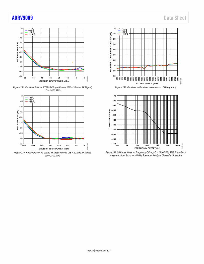
Figure 235. Receiver EVM vs. LTE20 RF Input Power, LTE = 20 MHz RF Signal, LO = 600 MHz
ADRV9009 Data Sheet
Rev. B | Page 62 of 127
–50
–45
–40
–35
–30
–25
–20
–15
–10
–5
0
–65 –55 –45 –35 –25 –15 –5 5
RE
CE
IVE
R E
VM
(d
B)
LTE20 RF INPUT POWER (dBm)
–40°C+25°C+110°C
16499-361
Figure 236. Receiver EVM vs. LTE20 RF Input Power, LTE = 20 MHz RF Signal, LO = 1800 MHz
–45
–40
–35
–30
–25
–20
–15
–10
–5
0
–65 –55 –45 –35 –25 –15 –5 5
RE
CE
IVE
R E
VM
(d
B)
LTE20 RF INPUT POWER (dBm)
–40°C+25°C+110°C
16499-362
Figure 237. Receiver EVM vs. LTE20 RF Input Power, LTE = 20 MHz RF Signal, LO = 2700 MHz
0
10
20
30
40
50
60
70
80
90
RE
CE
IVE
RT
O R
EC
EIV
ER
IS
OL
AT
ION
(d
B)
LO FREQUENCY (MHz)
–40°C+25°C+110°C
650
750
850
950
1050
1150
1250
1350
1450
1550
1650
1750
1850
1950
2050
2150
2250
2350
2450
2550
2650
2750
2850
16499-363
Figure 238. Receiver to Receiver Isolation vs. LO Frequency
–70
–80
–90
–100
–110
LO
PH
AS
E N
OIS
E (
dB
)
–120
–130
–140
–150
–160
–170
FREQUENCY OFFSET (Hz)100M100 1k 10k 100k 1M 10M
16499-364
Figure 239. LO Phase Noise vs. Frequency Offset, LO = 1900 MHz, RMS Phase Error Integrated from 2 kHz to 18 MHz, Spectrum Analyzer Limits Far Out Noise
Data Sheet ADRV9009
Rev. B | Page 63 of 127
3400 MHz TO 4800 MHz BAND
–4.0
–3.5
–3.0
–2.5
–2.0
–1.5
–1.0
–0.5
0
3400 3600 3800 4000 4200 4400 4600 4800 5000
TR
AN
SM
ITT
ER
PA
TH
LO
SS
(d
B)
LO FREQUENCY (MHz) 16499-365
Figure 240. Transmitter Path Loss vs. LO Frequency (Simulation), Can Be Used for De-Embedding Performance Data
0
1
2
3
4
5
6
7
8
9
10
3400 3600 3800 4000 4200 4400 4600 4800
TR
AN
SM
ITT
ER
CW
OU
TP
UT
PO
WE
R (
dB
m)
TRANSMITTER LO FREQUENCY (MHz)
Tx1 = –40°CTx2 = –40°CTx1 = +25°CTx2 = +25°CTx1 = +110°CTx2 = +110°C
16499-366
Figure 241. Transmitter CW Output Power vs. Transmitter LO Frequency, Transmitter QEC and External LO Leakage Active, Transmitter in
200 MHz/450 MHz Bandwidth Mode, IQ Rate = 491.52 MHz, Attenuation = 0 dB, Not De-Embedded
–100
–90
–80
–70
–60
–50
–40
–30
–20
–10
0
–50–100 0 50 100
TR
AN
SM
ITT
ER
IM
AG
E R
EJE
CT
ION
AC
RO
SS
LA
RG
E S
IGN
AL
BA
ND
WID
TH
(d
Bc)
BASEBAND OFFSET FREQUENCY AND ATTENUATION (MHz)
–40°C ATTENUATION = 0dB–40°C ATTENUATION = 5dB–40°C ATTENUATION = 10dB–40°C ATTENUATION = 15dB–40°C ATTENUATION = 20dB–40°C ATTENUATION = 25dB
+25°C ATTENUATION = 0dB+25°C ATTENUATION = 5dB+25°C ATTENUATION = 10dB+25°C ATTENUATION = 15dB+25°C ATTENUATION = 20dB+25°C ATTENUATION = 25dB
+110°C ATTENUATION = 0dB+110°C ATTENUATION = 5dB+110°C ATTENUATION = 10dB+110°C ATTENUATION = 15dB+110°C ATTENUATION = 20dB+110°C ATTENUATION = 25dB
16499-367
Figure 242. Transmitter Image Rejection Across Large Signal Bandwidth vs. Baseband Offset Frequency and Attenuation, QEC Trained with Three Tones
Placed at 10 MHz, 50 MHz, and 100 MHz (Tracking On), Total Combined Power = −6 dBFS, Correction Then Frozen (Tracking Turned Off), CW Tone
Swept Across Large Signal Bandwidth, LO = 3700 MHz
TR
AN
SM
ITT
ER
IM
AG
E R
EJE
CT
ION
AC
RO
SS
LA
RG
E S
IGN
AL
BA
ND
WID
TH
(d
Bc)
–100
–90
–80
–70
–60
–50
–40
–30
–20
–10
–50–100 0 50 100
BASEBAND OFFSET FREQUENCY (MHz)
–40°C ATTENUATION = 0dB–40°C ATTENUATION = 5dB–40°C ATTENUATION = 10dB–40°C ATTENUATION = 15dB–40°C ATTENUATION = 20dB–40°C ATTENUATION = 25dB
+25°C ATTENUATION = 0dB+25°C ATTENUATION = 5dB+25°C ATTENUATION = 10dB+25°C ATTENUATION = 15dB+25°C ATTENUATION = 20dB+25°C ATTENUATION = 25dB
+110°C ATTENUATION = 0dB+110°C ATTENUATION = 5dB+110°C ATTENUATION = 10dB+110°C ATTENUATION = 15dB+110°C ATTENUATION = 20dB+110°C ATTENUATION = 25dB
16499-368
Figure 243. Transmitter Image Rejection Across Large Signal Bandwidth vs. Baseband Offset Frequency and Attenuation, QEC Trained with Three Tones
(Tracking On), Total Combined Power = −6 dBFS, Correction Then Frozen (Tracking Turned Off), CW Tone Swept Across Large Signal Bandwidth,
LO = 4600 MHz
–1.0–0.9–0.8–0.7–0.6–0.5–0.4–0.3–0.2–0.1
0.00.10.20.30.40.50.60.70.80.91.0
–225 –175 –125 –75 –25 25 75 125 175 225
TR
AN
SM
ITT
ER
PA
SS
BA
ND
FL
AT
NE
SS
(d
B)
BASEBAND OFFSET FREQUENCY (MHz)
Tx1 = –40°CTx2 = –40°CTx1 = +25°CTx2 = +25°CTx1 = +110°CTx2 = +110°C
16499-369
Figure 244. Transmitter Pass Band Flatness vs. Baseband Offset Frequency, Off Chip Match Response De-Embedded, LO = 3600 MHz
–1.0–0.9–0.8–0.7–0.6–0.5–0.4–0.3–0.2–0.1
0.00.10.20.30.40.50.60.70.80.91.0
–225 –175 –125 –75 –25 25 75 125 175 225
TR
AN
SM
ITT
ER
PA
SS
BA
ND
FL
AT
NE
SS
(d
B)
BASEBAND OFFSET FREQUENCY (MHz)
Tx1 = –40°CTx2 = –40°CTx1 = +25°CTx2 = +25°CTx1 = +110°CTx2 = +110°C
16499-370
Figure 245. Transmitter Pass Band Flatness vs. Baseband Offset Frequency, Off Chip Match Response De-Embedded, LO = 4600 MHz
ADRV9009 Data Sheet
Rev. B | Page 64 of 127
–90
–88
–86
–84
–82
–80
–78
–76
–74
–72
–70
3700 4600
TR
AN
SM
ITT
ER
LO
LE
AK
AG
E (
dB
FS
)
TRANSMITTER LO FREQUENCY (MHz)
Tx1 = –40°CTx2 = –40°CTx1 = +25°CTx2 = +25°CTx1 = +110°CTx2 = +110°C
16499-371
Figure 246. Transmitter LO Leakage vs. Transmitter LO Frequency, Transmitter Attenuation = 0 dB
0
20
40
60
80
100
1203400 3600 3800 4000 4200 4400 4600 4800
TR
AN
SM
ITT
ER
TO
RE
CE
IVE
R
ISO
LAT
ION
(d
B)
RECEIVER LO FREQUENCY (MHz)
Tx1 TO Rx1Tx1 TO Rx2Tx2 TO Rx1Tx2 TO Rx2
16499-372
Figure 247. Transmitter to Receiver Isolation vs. Receiver LO Frequency, Temperature = −40°C, +25°C, and +110°C
0
100
30
10
70
80
50
40
20
60
90
TR
AN
SM
ITT
ER
TO
TR
AN
SM
ITT
ER
ISO
LA
TIO
N (
dB
)
3400 4800460040003600 4200 44003800
TRANSMITTER LO FREQUENCY (MHz)
Tx1 TO Tx2 0dBTx2 TO Tx1 0dB
16499-751
Figure 248. Transmitter to Transmitter Isolation vs. Transmitter LO Frequency, Temperature = 25°C
–145
–175
–165
–155
–160
–150
–170
TR
AN
SM
ITT
ER
NO
ISE
(d
Bm
/Hz)
TRANSMITTER ATTENUATOR SETTING (dB)
0 6 14 192 104 12 16 181 85 1393 11 15 177
4600MHz = +110°C4600MHz = +25°C4600MHz = –40°C3600MHz = +110°C3600MHz = +25°C3600MHz = –40°C
16499-752
Figure 249. Transmitter Noise vs. Transmitter Attenuator Setting
40
–10
25
35
0
5
15
20
30
10
–5
TR
AN
SM
ITT
ER
OIP
3, R
IGH
T (
dB
m)
0 301262 168 14 1810 22 2624 28204
TRANSMITTER ATTENUATOR SETTING (dB)
+110°C+25°C–40°C
16499-753
Figure 250. Transmitter OIP3, Right vs. Transmitter Attenuator Setting, LO = 3600 MHz, Total RMS Power = −12 dBFS
35
–10
25
0
5
15
20
30
10
–5
TR
AN
SM
ITT
ER
OIP
3, R
IGH
T (
dB
m)
0 301262 168 14 1810 22 2624 28204
TRANSMITTER ATTENUATOR SETTING (dB)
+110°C+25°C–40°C
16499-754
Figure 251. Transmitter OIP3, Right vs. Transmitter Attenuator Setting, LO = 4600 MHz, Total RMS Power = −12 dBFS
Data Sheet ADRV9009
Rev. B | Page 65 of 127
40
35
0
25
5
15
20
30
10
TR
AN
SM
ITT
ER
OIP
3 R
IGH
T (
dB
m)
510
95100
6570
3540
1520
8590
4550
7580
5560
2530
BASEBAND TONE PAIR SWEPT ACROSS PASS BAND (MHz)
Tx1 = +110°CTx1 = +25°CTx1 = –40°CTx2 = +110°CTx2 = +25°CTx2 = –40°C
16499-755
Figure 252. Transmitter OIP3 Right vs. Baseband Tone Pair Swept Across Pass Band, LO = 3600 MHz, Total RMS Power = −12 dBFS
40
35
0
25
5
15
20
30
10
TR
AN
SM
ITT
ER
OIP
3 R
IGH
T (
dB
m)
510
95100
6570
3540
1520
8590
4550
7580
5560
2530
BASEBAND TONE PAIR SWEPT ACROSS PASS BAND (MHz)
Tx1 = +110°CTx1 = +25°CTx1 = –40°CTx2 = +110°CTx2 = +25°CTx2 = –40°C
16499-756
Figure 253. Transmitter OIP3 Right vs. Baseband Tone Pair Swept Across Pass Band, LO = 4600 MHz, Total RMS Power = −12 dBFS
0
–20
–120
–60
–100
–80
–40
TR
AN
SM
ITT
ER
HD
2 (d
Bc)
0 3222102 3014 26186 24124 16 28208
TRANSMITTER ATTENUATOR SETTING (dB)
+110°C = HD2+25°C = HD2–40°C = HD2+110°C = UPPER HD2+25°C = UPPER HD2 –40°C = UPPER HD2
16499-757
Figure 254. Transmitter HD2 vs. Transmitter Attenuator Setting, Baseband Frequency = 10 MHz, LO = 3600 MHz, CW = −15 dBFS
0
–20
–120
–60
–100
–80
–40
TR
AN
SM
ITT
ER
HD
2 (d
Bc)
0 3222102 3014 26186 24124 16 28208
TRANSMITTER ATTENUATOR SETTING (dB)
+110°C = HD2+25°C = HD2–40°C = HD2+110°C = UPPER HD2+25°C = UPPER HD2 –40°C = UPPER HD2
16499-758
Figure 255. Transmitter HD2 vs. Transmitter Attenuator Setting, Baseband Frequency = 10 MHz, LO = 4600 MHz, CW = −15 dBFS
0
–20
–120
–60
–100
–80
–40
TR
AN
SM
ITT
ER
HD
3 (d
Bc)
0 3222102 3014 26186 24124 16 28208TRANSMITTER ATTENUATOR SETTING (dB)
Tx1 = +110°CTx1 = +25°CTx1 = –40°CTx2 = +110°CTx2 = +25°CTx2 = –40°C
16499-759
Figure 256. Transmitter HD3 vs. Transmitter Attenuator Setting, LO = 3600 MHz, CW = −15 dBFS, Baseband Frequency = 10 MHz
0
–20
–120
–60
–100
–80
–40
TR
AN
SM
ITT
ER
HD
3 (d
Bc)
0 3222102 3014 26186 24124 16 28208TRANSMITTER ATTENUATOR SETTING (dB)
Tx1 = +110°CTx1 = +25°CTx1 = –40°CTx2 = +110°CTx2 = +25°CTx2 = –40°C
16499-760
Figure 257. Transmitter HD3 vs. Transmitter Attenuator Setting, LO = 4600 MHz, CW = −15 dBFS, Baseband Frequency = 10 MHz
ADRV9009 Data Sheet
Rev. B | Page 66 of 127
0
–20
–120
–60
–100
–80
–40
TR
AN
SM
ITT
ER
HD
3 IM
AG
E (
dB
c)A
PP
EA
RS
ON
SA
ME
SID
E A
S D
ES
IRE
D S
IGN
AL
0 20102 14 186 124 168TRANSMITTER ATTENUATOR SETTING (dB)
Tx1 = +110°CTx1 = +25°CTx1 = –40°CTx2 = +110°CTx2 = +25°CTx2 = –40°C
16499-761
Figure 258. Transmitter HD3 Image Appears on Same Side as Desired Signal vs. Transmitter Attenuator Setting, LO = 3600 MHz, CW = −15 dBFS
0
–20
–120
–60
–100
–80
–40
TR
AN
SM
ITT
ER
HD
3 IM
AG
E (
dB
c)A
PP
EA
RS
ON
SA
ME
SID
E A
S D
ES
IRE
D S
IGN
AL
0 20102 14 186 124 168TRANSMITTER ATTENUATOR SETTING (dB)
Tx1 = +110°CTx1 = +25°CTx1 = –40°CTx2 = +110°CTx2 = +25°CTx2 = –40°C
16499-762
Figure 259. Transmitter HD3 Image Appears on Same Side as Desired Signal vs. Transmitter Attenuator Setting, LO = 4600 MHz, CW = −15 dBFS
0.05
0.04
–0.05
0
–0.04
–0.02
0.02
0.03
–0.01
–0.03
0.01
TR
AN
SM
ITT
ER
AT
TE
NU
AT
OR
ST
EP
ER
RO
R (
dB
)
0 3222102 3014 26186 24124 16 28208
TRANSMITTER ATTENUATOR SETTING (dB)
+110°C+25°C–40°C
16499-763
Figure 260. Transmitter Attenuator Step Error vs. Transmitter Attenuator Setting, LO = 3600 MHz
0.05
0.04
–0.05
0
–0.04
–0.02
0.02
0.03
–0.01
–0.03
0.01
TR
AN
SM
ITT
ER
AT
TE
NU
AT
OR
ST
EP
ER
RO
R (
dB
)
0 3222102 3014 26186 24124 16 28208
TRANSMITTER ATTENUATOR SETTING (dB)
+110°C+25°C–40°C
16499-764
Figure 261. Transmitter Attenuator Step Error vs. Transmitter Attenuator Setting, LO = 4600 MHz
–30
–32
–50
–40
–48
–44
–36
–34
–42
–46
–38
EV
M (
dB
)
0 255 1510 20
TRANSMITTER ATTENUATION (dBm)
+110°C+25°C–40°C
16499-765
Figure 262. EVM vs. Transmitter Attenuation, LTE = 20 MHz Signal Centered on DC, LO = 3600 MHz
–30
–32
–50
–40
–48
–44
–36
–34
–42
–46
–38
EV
M (
dB
)
0 255 1510 20
TRANSMITTER ATTENUATION (dBm)
+110°C+25°C–40°C
16499-766
Figure 263. EVM vs. Transmitter Attenuation, LTE = 20 MHz Signal Centered on DC, LO = 4600 MHz
Data Sheet ADRV9009
Rev. B | Page 67 of 127
–10
–20
–100
–60
–80
–40
–30
–70
–90
–50
AM
PL
ITU
DE
(d
Bm
)
4100
5100
4300
4700
4500
4900
5000
4200
4600
4400
4800
FREQUENCY (MHz)
Tx OUTPUTANALYZER NO SIGNAL
16499-767
Figure 264. Amplitude vs. Frequency, Transmitter Output Spurious, Transmitter 1 = 4600 MHz, LTE = 5 MHz, Offset = 10 MHz, RMS Ripple in Noise
Floor Due to Spectrum Analyzer = −12 dBFS, Temperature = 25°C
–2.0
–1.8
–1.6
–1.4
–1.2
–1.0
–0.8
–0.6
–0.4
–0.2
0
3400 3600 3800 4000 4200 4400 4600 4800 5000
OB
SE
RV
AT
ION
RE
CE
IVE
R O
FF
CH
IPM
AT
CH
ING
CIR
CU
ITP
AT
H L
OS
S (
dB
)
LO FREQUENCY (MHz) 16499-768
Figure 265. Observation Receiver Off Chip Matching Circuit Path Loss vs. LO Frequency, Simulation, Can be Used for De-Embedding Performance Data
0
–10
–100
–50
–70
–30
–20
–60
–90
–80
–40
OB
SE
RV
AT
ION
RE
CE
IVE
R L
O L
EA
KA
GE
(d
Bm
)
LO FREQUENCY (MHz)
3600 4600
+110°C+25°C–40°C
16499-769
Figure 266. Observation Receiver LO Leakage vs. LO Frequency, from 3600 MHz to 4600 MHz
30
32
28
26
18
22
24
14
16
20
OB
SE
RV
AT
ION
RE
CE
IVE
R N
OIS
E F
IGU
RE
(d
B)
OBSERVATION RECEIVER ATTENUATOR SETTING (dB)
0 10987654321
+110°C+25°C–40°C
16499-770
Figure 267. Observation Receiver Noise Figure vs. Observation Receiver Attenuator Setting, LO = 3600 MHz, Total Nyquist Integration Bandwidth
34
32
14
24
16
28
30
20
18
22
26
OB
SE
RV
AT
ION
RE
CE
IVE
R N
OIS
E F
IGU
RE
(d
B)
OBSERVATION RECEIVER ATTENUATOR SETTING (dB)
0 10987654321
+110°C+25°C–40°C
16499-771
Figure 268. Observation Receiver Noise Figure vs. Observation Receiver Attenuator Setting, LO = 4600 MHz, Total Nyquist Integration Bandwidth
80
40
60
70
50
75
55
65
45OB
SE
RV
AT
ION
RE
CE
IVE
R I
IP2,
SU
MA
ND
DIF
FE
RE
NC
E P
RO
DC
UT
S (
dB
m)
f1 OFFSET FREQUENCY (MHz)
36063605
36663665
37463745
38263825
37863785
38063805
37663765
36263625
37063705
36863685
36463645
37263725
IIP2 SUM +110°CIIP2 SUM +25°CIIP2 SUM –40°CIIP2 DIFF +110°CIIP2 DIFF +25°CIIP2 DIFF –40°C
16499-772
Figure 269. Observation Receiver IIP2, Sum and Difference Products vs. f1 Offset Frequency, Tones Separated by 1 MHz Swept Across Pass Band at
−22 dBm Each, LO = 3600 MHz, Attenuation = 0 dB
ADRV9009 Data Sheet
Rev. B | Page 68 of 127
80
40
60
70
50
75
55
65
45
OB
SE
RV
AT
ION
RE
CE
IVE
R I
IP2,
SU
M A
ND
DIF
FE
RE
NC
E P
RO
DU
CT
S (
dB
m)
f1 OFFSET FREQUENCY (MHz)
46064605
46664665
47464745
48264825
47864785
48064805
47664765
46264625
47064705
46864685
46464645
47264725
IIP2 SUM +110°CIIP2 SUM +25°CIIP2 SUM –40°CIIP2 DIFF +110°CIIP2 DIFF +25°CIIP2 DIFF –40°C
16499-773
Figure 270. Observation Receiver IIP2, Sum and Difference Products vs. f1 Offset Frequency, Tones Separated By 1 MHz Swept Across Pass Band at
−22 dBm Each, 4600 MHz, Attenuation = 0 dB
80
50
75
55
65
60
70
OB
SE
RV
AT
ION
RE
CE
IVE
R I
IP2,
SU
M A
ND
DIF
FE
RE
NC
E P
RO
DU
CT
S (
dB
m)
ATTENUATION (dB)
0 108642
IIP2 SUM +110°CIIP2 SUM +25°CIIP2 SUM –40°CIIP2 DIFF +110°CIIP2 DIFF +25°CIIP2 DIFF –40°C
16499-774
Figure 271. Observation Receiver IIP2, Sum and Difference Products vs. Attenuation, LO = 3600 MHz, Tone 1 = 3645 MHz, Tone 2 = 3646 MHz at
−22 dBm Plus Attenuation
80
50
75
55
65
60
70
OB
SE
RV
AT
ION
RE
CE
IVE
R I
IP2,
SU
M A
ND
DIF
FE
RE
NC
E P
RO
DU
CT
S (
dB
m)
ATTENUATION (dB)
0 108642
IIP2 SUM +110°CIIP2 SUM +25°CIIP2 SUM –40°CIIP2 DIFF +110°CIIP2 DIFF +25°CIIP2 DIFF –40°C
16499-775
Figure 272. Observation Receiver IIP2, Sum and Difference Products vs. Attenuation, LO = 4600 MHz, Tone 1 = 4645 MHz, Tone 2 = 4646 MHz at
−22 dBm Plus Attenuation
80
0
20
50
70
40
60
10
30
OB
SE
RV
AT
ION
RE
CE
IVE
R I
IP2,
f1
– f2
(d
Bm
)
IIP2 SUM +110°CIIP2 SUM +25°CIIP2 SUM –40°CIIP2 DIFF +110°CIIP2 DIFF +25°CIIP2 DIFF –40°C
361
2
363
2
365
2
367
2
369
2
371
2
373
2
375
2
377
2
379
2
381
2
383
2
INTERMODULATION FREQUENCY (MHz) 16499-776
Figure 273. Observation Receiver IIP2, f1 − f2 vs. Intermodulation Frequency, LO = 3600 MHz, Tone 1 = 3602 MHz, Tone 2 Swept, −22 dBm Each,
Attenuation = 0 dB
80
0
20
50
70
40
60
10
30
OB
SE
RV
AT
ION
RE
CE
IVE
R I
IP2,
f1
– f2
(d
Bm
)
IIP2 SUM +110°CIIP2 SUM +25°CIIP2 SUM –40°CIIP2 DIFF +110°CIIP2 DIFF +25°CIIP2 DIFF –40°C
4612
4632
4652
4672
4692
4712
4732
4752
4772
4792
4812
4832
INTERMODULATION FREQUENCY (MHz) 16499-777
Figure 274. Observation Receiver IIP2, f1 − f2 vs. Intermodulation Frequency, LO = 4600 MHz, Tone 1 = 4602 MHz, Tone 2 Swept, −22 dBm Each,
Attenuation = 0 dB
80
50
75
55
65
60
70
OB
SE
RV
AT
ION
RE
CE
IVE
R I
IP2,
f1
– f2
(d
Bm
)
ATTENUATION (dB)
0 108642
IIP2 SUM +110°CIIP2 SUM +25°CIIP2 SUM –40°CIIP2 DIFF +110°CIIP2 DIFF +25°CIIP2 DIFF –40°C
16499-778
Figure 275. Observation Receiver IIP2, f1 − f2 vs. Attenuation, LO = 3600 MHz, Tone 1 = 3602 MHz, Tone 2 = 3702 MHz at −22 dBm Plus Attenuation
Data Sheet ADRV9009
Rev. B | Page 69 of 127
80
50
75
55
65
60
70
OB
SE
RV
AT
ION
RE
CE
IVE
R I
IP2,
f1
– f2
(d
Bm
)
ATTENUATION (dB)
0 108642
INPUT IP2 SUM +110°CINPUT IP2 SUM +25°CINPUT IP2 SUM –40°CINPUT IP2 DIFF +110°CINPUT IP2 DIFF +25°CINPUT IP2 DIFF –40°C
16499-779
Figure 276. Observation Receiver IIP2, f1 − f2 vs. Attenuation, LO = 4600 MHz, Tone 1 = 4602 MHz, Tone 2 = 4612 MHz at −22 dBm Plus
Attenuation
25
0
5
15
20
10
OB
SE
RV
AT
ION
RE
CE
IVE
R I
IP3,
2f1
– f
2 (d
Bm
)
ORx1 = +110°CORx1 = +25°CORx1 = –40°C
3605 3625 3645 3665 3685 3705 3725 3745 3765 3785 3805 38253606 3626 3646 3666 3686 3706
f1 OFFSET FREQUENCY (MHz)
3726 3746 3766 3786 3806 3826
16499-780
Figure 277. Observation Receiver IIP3, 2f1 − f2 vs. f1 Offset Frequency, LO = 3600 MHz, Attenuation = 0 dB, Tones Separated by 1 MHz Swept Across Pass
Band at −22 dBm Each
25
0
5
15
20
10
OB
SE
RV
AT
ION
RE
CE
IVE
R I
IP3,
2f1
– f
2 (d
Bm
)
f1 OFFSET FREQUENCY (MHz)
ORx1 = +110°CORx1 = +25°CORx1 = –40°C
4606 4626 4646 4666 4686 4706 4726 4746 4766 4786 4806 48264605 4625 4645 4665 4685 4705 4725 4745 4765 4785 4805 4825
16499-781
Figure 278. Observation Receiver IIP3, 2f1 − f2 vs. f1 Offset Frequency, LO = 4600 MHz, Attenuation = 0 dB, Tones Separated by 1 MHz Swept Across Pass
Band at −22 dBm Each
30
6
26
10
18
14
22
28
24
8
16
12
20
OB
SE
RV
AT
ION
RE
CE
IVE
R I
IP3,
2f1
– f
2 (d
Bm
)
ATTENUATION (dB)
0 108642
INPUT IP3 = +110°CINPUT IP3 = +25°CINPUT IP3 = –40°C
16499-782
Figure 279. Observation Receiver IIP3, 2f1 − f2 vs. Attenuation, LO = 3600 MHz, Tone 1 = 3695 MHz, Tone 2 = 3696 MHz at −22 dBm Plus Attenuation
30
6
26
10
18
14
22
28
24
8
16
12
20O
BS
ER
VA
TIO
N R
EC
EIV
ER
IIP
3, 2
f1 –
f2
(dB
m)
ATTENUATION (dB)
0 108642
INPUT IP3 = +110°CINPUT IP3 = +25°CINPUT IP3 = –40°C
16499-783
Figure 280. Observation Receiver IIP3, 2f1 − f2 vs. Attenuation, LO = 4600 MHz, Tone 1 = 4695 MHz, Tone 2 = 4696 MHz at −22 dBm Plus Attenuation
30
0
10
INTERMODULATION FREQUENCY (MHz)
25
20
5
15
OB
SE
RV
AT
ION
RE
CE
IVE
R I
IP3,
2f1
– f
2 (d
Bm
)
INPUT IP3 SUM +110°CINPUT IP3 SUM +25°CINPUT IP3 SUM –40°CINPUT IP3 DIFF +110°CINPUT IP3 DIFF +25°CINPUT IP3 DIFF –40°C
361
2
363
2
365
2
367
2
369
2
371
2
373
2
375
2
377
2
379
2
381
2
383
216499-784
Figure 281. Observation Receiver IIP3, 2f1 − f2 vs. Intermodulation Frequency, LO = 3600 MHz, Tone 1 = 3602 MHz, Tone 2 = Swept,
−22 dBm Each
ADRV9009 Data Sheet
Rev. B | Page 70 of 127
30
0
10
25
20
5
15
OB
SE
RV
AT
ION
RE
CE
IVE
R I
IP3,
2f1
– f
2 (d
Bm
)
IIP3 SUM +110°CIIP3 SUM +25°CIIP3 SUM –40°CIIP3 DIFF +110°CIIP3 DIFF +25°CIIP3 DIFF –40°C
4612
4632
4652
4672
4692
4712
4732
4752
4772
4792
4812
4832
INTERMODULATION FREQUENCY (MHz) 16499-785
Figure 282. Observation Receiver IIP3, 2f1 − f2 vs. Intermodulation Frequency, LO = 4600 MHz, Tone 1 = 4602 MHz, Tone 2 = Swept, −22 dBm Each
OB
SE
RV
AT
ION
RE
CE
IVE
R I
IP3,
2f1
– f
2 (d
Bm
)
ATTENUATION (dB)
0 108642
30
6
26
10
18
14
22
28
24
8
16
12
20
IIP3 = +110°CIIP3 = +25°CIIP3 = –40°C
16499-786
Figure 283. Observation Receiver IIP3, 2f1 − f2 vs. Attenuation, LO = 3600 MHz, Tone 1 = 3602 MHz, Tone 2 = 3722 MHz, −22 dBm Each Plus Attenuation
OB
SE
RV
AT
ION
RE
CE
IVE
R I
IP3,
2f1
– f
2 (d
Bm
)
ATTENUATION (dB)
0 108642
30
6
26
10
18
14
22
28
24
8
16
12
20
IIP3 = +110°CIIP3 = +25°CIIP3 = –40°C
16499-787
Figure 284. Observation Receiver IIP3, 2f1 − f2 vs. Attenuation, LO = 4600 MHz, Tone 1 = 4602 MHz, Tone 2 = 4722 MHz at −22 dBm Plus
Attenuation Each
0
–100
–90
–80
–70
–60
–50
–40
–30
–20
–10
–225
–175
–125 –7
5 0
–25
–200
–150
–100 –5
0 25 75
125
225
17550
100
150
200
BASEBAND FREQUENCY OFFSET (MHz)
+110°C = 10dB+25°C = 10dB–40°C = 10dB+110°C = 0dB+25°C = 0dB–40°C = 0dB
16499-788
OB
SE
RV
AT
ION
RE
CE
IVE
RIM
AG
E R
EJE
CT
ION
(d
Bc)
Figure 285. Observation Receiver Image Rejection vs. Baseband Frequency Offset, CW Signal Swept Across the Band, LO = 3600 MHz
0
–100
–90
–80
–70
–60
–50
–40
–30
–20
–10
–225
–175
–125 –7
5 0
–25
–200
–150
–100 –5
0 25 75 125
225
17550 100
150
200
BASEBAND FREQUENCY OFFSET (MHz)
+110°C = 10dB+25°C = 10dB–40°C = 10dB+110°C = 0dB+25°C = 0dB–40°C = 0dB
16499-789
OB
SE
RV
AT
ION
RE
CE
IVE
RIM
AG
E R
EJE
CT
ION
(d
Bc)
Figure 286. Observation Receiver Image Rejection vs. Baseband Frequency Offset, CW Signal Swept Across the Band, LO = 4600 MHz
OB
SE
RV
AT
ION
RE
CE
IVE
R G
AIN
(d
Bm
)
OBSERVATION RECEIVER ATTENUATION (dB)
0 1086421 9753
18
4
14
6
10
16
12
8
+110°C+25°C–40°C
16499-790
Figure 287. Observation Receiver Gain vs. Observation Receiver Attenuation, LO = 3600 MHz
Data Sheet ADRV9009
Rev. B | Page 71 of 127
OB
SE
RV
AT
ION
RE
CE
IVE
R G
AIN
(d
Bm
)
OBSERVATION RECEIVER ATTENUATION (dB)
0 1086421 9753
18
4
14
6
10
16
12
8
+110°C+25°C–40°C
16499-791
Figure 288. Observation Receiver Gain vs. Observation Receiver Attenuation, LO = 4600 MHz
OBSERVATION RECEIVER ATTENUATOR SETTING (dB)
0 1086421 9753
+110°C+25°C–40°C
0.5
–0.5
–0.4
–0.3
–0.2
–0.1
0.1
0
0.2
0.3
0.4
OB
SE
RV
AT
ION
RE
CE
IVE
R G
AIN
ST
EP
ER
RO
R (
dB
)
16499-792
Figure 289. Observation Receiver Gain Step Error vs. Observation Receiver Attenuator Setting, LO = 3600 MHz
OBSERVATION RECEIVER ATTENUATOR SETTING (dB)
0 1086421 9753
+110°C+25°C–40°C
0.5
–0.5
–0.4
–0.3
–0.2
–0.1
0.1
0
0.2
0.3
0.4
OB
SE
RV
AT
ION
RE
CE
IVE
R G
AIN
ST
EP
ER
RO
R (
dB
)
16499-793
Figure 290. Observation Receiver Gain Step Error vs. Observation Receiver Attenuator Setting, LO = 4600 MHz
–225
–175
–125 –7
5 0
–25
–200
–150
–100 –5
0 25 75 125
225
17550 100
150
200
BASEBAND FREQUENCY OFFSET (MHz)
+110°C+25°C–40°C
0.5
–0.5
–0.4
–0.3
–0.2
–0.1
0.1
0
0.2
0.3
0.4
OB
SE
RV
AT
ION
RE
CE
IVE
R P
AS
S B
AN
DF
LA
TN
ES
S (
dB
)
16499-794
Figure 291. Observation Receiver Pass Band Flatness vs. Baseband Frequency Offset, LO = 3600 MHz
–225
–175
–125 –7
5 0
–25
–200
–150
–100 –5
0 25 75 125
225
17550 100
150
200
BASEBAND FREQUENCY OFFSET (MHz)
+110°C+25°C–40°C
0.5
–0.5
–0.4
–0.3
–0.2
–0.1
0.1
0
0.2
0.3
0.4
OB
SE
RV
AT
ION
RE
CE
IVE
R P
AS
S B
AN
DF
LA
TN
ES
S (
dB
)
16499-795
Figure 292. Observation Receiver Pass Band Flatness vs. Baseband Frequency Offset, LO = 4600 MHz
OB
SE
RV
AT
ION
RE
CE
IVE
R D
C O
FF
SE
T (
dB
FS
)
ATTENUATION (dB)
0 105
0
–120
–40
–80
–20
–60
–100
INPUT IP3 = +110°CINPUT IP3 = +25°CINPUT IP3 = –40°C
16499-796
Figure 293. Observation Receiver DC Offset vs. Attenuation, LO = 3600 MHz
ADRV9009 Data Sheet
Rev. B | Page 72 of 127
OB
SE
RV
AT
ION
RE
CE
IVE
R D
C O
FF
SE
T (
dB
FS
)
ATTENUATION (dB)
0 105
0
–120
–40
–80
–20
–60
–100
INPUT IP3 = +110°CINPUT IP3 = +25°CINPUT IP3 = –40°C
16499-797
Figure 294. Observation Receiver DC Offset vs. Attenuation, LO = 4600 MHz
0
–120
–80
–100
–60
–40
–20
–100 –75 –50 –25 0 25 50 10075
OB
SE
RV
AT
ION
RE
CE
IVE
R H
D2
(dB
c)
OFFSET FREQUENCY (MHz)
+110°C = 0 (RIGHT)+110°C = 11.5 (RIGHT)+110°C = 0 (LEFT)+110°C = 11.5 (LEFT)+25°C = 0 (RIGHT)+25°C = 11.5 (RIGHT)
+25°C = 0 (LEFT)+25°C = 11.5 (LEFT)–40°C = 0 (RIGHT)–40°C = 11.5 (RIGHT)–40°C = 0 (LEFT)–40°C = 11.5 (LEFT)
16499-798
Figure 295. Observation Receiver HD2 vs. Offset Frequency, LO = 3600 MHz, Tone Level = −20 dBm Plus Attenuation
0
–120
–80
–100
–60
–40
–20
–100 –75 –50 –25 0 25 50 10075
OB
SE
RV
AT
ION
RE
CE
IVE
R H
D2
(dB
c)
OFFSET FREQUENCY (MHz)
+110°C = 0 (RIGHT)+110°C = 11.5 (RIGHT)+110°C = 0 (LEFT)+110°C = 11.5 (LEFT)+25°C = 0 (RIGHT)+25°C = 11.5 (RIGHT)
+25°C = 0 (LEFT)+25°C = 11.5 (LEFT)–40°C = 0 (RIGHT)–40°C = 11.5 (RIGHT)–40°C = 0 (LEFT)–40°C = 11.5 (LEFT)
16499-799
Figure 296. Observation Receiver HD2 vs. Offset Frequency, LO = 4600 MHz, Tone Level = −20 dBm Plus Attenuation
0
–100
–30
–10
–70
–50
–40
–20
–60
–80
–90
OB
SE
RV
AT
ION
RE
CE
IVE
R H
D3,
LE
FT
AN
D R
IGH
T (
dB
c)
–90.0 90.045.0–22.5–67.5 67.522.5–45.0
OFFSET FREQUENCY (MHz)
HD3 RIGHT dBc = +110°CHD3 RIGHT dBc = +25°CHD3 RIGHT dBc = –40°CHD3 LEFT dBc = = +110°CHD3 LEFT dBc = +25°CHD3 LEFT dBc = –40°C
16499-800
Figure 297. Observation Receiver HD3, Left and Right vs. Offset Frequency, LO = 3600 MHz, Tone Level = −20 dBm
0
–100
–30
–10
–70
–50
–40
–20
–60
–80
–90
OB
SE
RV
AT
ION
RE
CE
IVE
R H
D3,
LE
FT
AN
D R
IGH
T (
dB
c)
–90.0 90.045.0–22.5–67.5 67.522.5–45.0
OFFSET FREQUENCY (MHz)
HD3 RIGHT dBc = +110°CHD3 RIGHT dBc = +25°CHD3 RIGHT dBc = –40°CHD3 LEFT dBc = = +110°CHD3 LEFT dBc = +25°CHD3 LEFT dBc = –40°C
16499-801
Figure 298. Observation Receiver HD3, Left and Right vs. Offset Frequency, LO = 4600 MHz, Tone Level = −20 dBm
0
140
120
80
40
20
100
60
TR
AN
SM
ITT
ER
TO
OB
SE
RV
AT
ION
RE
CE
IVE
RIS
OL
AT
ION
(d
B)
LO FREQUENCY (MHz)
3400 4200 48003800 460040003600 4400
Tx1 TO ORx1Tx2 TO ORx1Tx1 TO ORx2Tx2 TO ORx2
16499-802
Figure 299. Transmitter to Observation Receiver Isolation vs. LO Frequency, Temperature = 25°C
Data Sheet ADRV9009
Rev. B | Page 73 of 127
0
–2.0
–0.8
–0.4
–0.6
–0.2
–1.2
–1.8
–1.4
–1.6
–1.0
RE
CE
IVE
R O
FF
CH
IP M
AT
CH
ING
CIR
CU
IT P
AT
H L
OS
S (
dB
)
LO FREQUENCY (MHz)
3400 4200 50003800 46004000 48003600 4400
16499-803
Figure 300. Receiver Off Chip Matching Circuit Path Loss vs. LO Frequency, (Simulation), Can Be Used for De-Embedding Performance Data
0
–10
–100
–50
–70
–30
–20
–60
–90
–80
–40
RE
CE
IVE
R L
O L
EA
KA
GE
(d
Bm
)
RECEIVER LO FREQUENCY (MHz)
3600 4600
+110°C+25°C–40°C
16499-804
Figure 301. Receiver LO Leakage vs. Receiver LO Frequency, Receiver Attenuation = 0 dB, RF Bandwidth = 200 MHz, Sample Rate = 245.76 MSPS
45
40
0
20
30
35
10
5
15
25
RE
CE
IVE
R N
OIS
E F
IGU
RE
(d
B)
RECEIVER ATTENUATION (dB)
0 2018161412108642
+110°C+25°C–40°C
16499-805
Figure 302. Receiver Noise Figure vs. Receiver Attenuation, LO = 3600 MHz, Receiver Bandwidth = 200 MHz, Sample Rate = 245.76 MSPS, Integration
Bandwidth = 500 kHz to 100 MHz
45
40
0
20
30
35
10
5
15
25
RE
CE
IVE
R N
OIS
E F
IGU
RE
(d
B)
RECEIVER ATTENUATION (dB)
0 2018161412108642
+110°C+25°C–40°C
16499-806
Figure 303. Receiver Noise Figure vs. Receiver Attenuation, LO = 4600 MHz, Bandwidth = 200 MHz, Sample Rate = 245.76 MSPS, Integration Bandwidth
= 500 kHz to 100 MHz
RE
CE
IVE
R I
IP2
(dB
m)
RECEIVER ATTENUATION (dB)
INPUT IP2 SUM +110°CINPUT IP2 SUM +25°CINPUT IP2 SUM –40°CINPUT IP2 DIFF +110°CINPUT IP2 DIFF +25°CINPUT IP2 DIFF –40°C
120
50
80
100
60
110
70
90
0 282624222018161412108642 30
16499-807
Figure 304. Receiver IIP2 vs. Receiver Attenuation, LO = 3600 MHz, Tones Placed at 3645 MHz and 3646 MHz, −21 dBm Plus Attenuation
RE
CE
IVE
R I
IP2
(dB
m)
RECEIVER ATTENUATION (dB)
INPUT IP2 SUM +110°CINPUT IP2 SUM +25°CINPUT IP2 SUM –40°CINPUT IP2 DIFF +110°CINPUT IP2 DIFF +25°CINPUT IP2 DIFF –40°C
110
50
80
100
60
70
90
0 282624222018161412108642 30
16499-808
Figure 305. Receiver IIP2 vs. Receiver Attenuation, LO = 4600 MHz, Tones Placed at 4645 MHz and 4646 MHz, −21 dBm Plus Attenuation
ADRV9009 Data Sheet
Rev. B | Page 74 of 127
RE
CE
IVE
R I
IP2
SU
M A
ND
DIF
FE
RE
NC
E A
CR
OS
SB
AN
DW
IDT
H (
dB
m)
IIP2 SUM +110°CIIP2 SUM +25°CIIP2 SUM –40°CIIP2 DIFF +110°CIIP2 DIFF +25°CIIP2 DIFF –40°C
80
40
55
75
45
50
65
70
60
36063605
36863685
36663665
36463645
36263625
37063705
SWEPT PASS BAND FREQUENCY (MHz) 16499-809
Figure 306. Receiver IIP2 Sum and Difference Across Bandwidth vs. Swept Pass Band Frequency, Receiver Attenuation = 0 dB, LO = 3600 MHz, Six Tone
Pairs, −21 dBm Each Plus Attenuation
RE
CE
IVE
R I
IP2
SU
M A
ND
DIF
FE
RE
NC
E A
CR
OS
SB
AN
DW
IDT
H (
dB
m)
IIP2 SUM +110°CIIP2 SUM +25°CIIP2 SUM –40°CIIP2 DIFF +110°CIIP2 DIFF +25°CIIP2 DIFF –40°C
80
40
55
75
45
50
65
70
60
46064605
46864685
46664665
46464645
46264625
47064705
SWEPT PASS BAND FREQUENCY (MHz) 16499-810
Figure 307. Receiver IIP2 Sum and Difference Across Bandwidth vs. Swept Pass Band Frequency, Receiver Attenuation = 0 dB, LO = 4600 MHz, Six Tone
Pairs, −21 dBm Each
RE
CE
IVE
R I
IP2
(dB
m)
100
80
50
55
75
90
85
95
65
70
60
0 2015105 3025RECEIVER ATTENUATION
+110°C = Rx1 (DIFF)+110°C = Rx1 (SUM)+25°C = Rx1 (DIFF)+25°C = Rx1 (SUM)–40°C = Rx1 (DIFF)–40°C = Rx1 (SUM)
+110°C = Rx2 (DIFF)+110°C = Rx2 (SUM)+25°C = Rx2 (DIFF)+25°C = Rx2 (SUM)–40°C = Rx2 (DIFF)–40°C = Rx2 (SUM)
16499-811
Figure 308. Receiver IIP2 vs. Receiver Attenuation, LO = 3600 MHz, Tones Placed at 3602 MHz and 3692 MHz, −21 dBm Plus Attenuation
RE
CE
IVE
R I
IP2
(dB
m)
100
80
50
55
75
90
85
95
65
70
60
0 2015105 3025RECEIVER ATTENUATION
+110°C = Rx1 (DIFF)+110°C = Rx1 (SUM)+25°C = Rx1 (DIFF)+25°C = Rx1 (SUM)–40°C = Rx1 (DIFF)–40°C = Rx1 (SUM)
+110°C = Rx2 (DIFF)+110°C = Rx2 (SUM)+25°C = Rx2 (DIFF)+25°C = Rx2 (SUM)–40°C = Rx2 (DIFF)–40°C = Rx2 (SUM)
16499-812
Figure 309. Receiver IIP2 vs. Receiver Attenuation, LO = 4600 MHz, Tones Placed at 4602 MHz and 4692 MHz, −21dBm Plus Attenuation
RE
CE
IVE
R I
IP2
SU
M A
ND
DIF
FE
RE
NC
E A
CR
OS
SB
AN
DW
IDT
H (
dB
m)
100
80
50
55
75
90
85
95
65
70
60
3612 3692367236523632 3682366236423622 37123702
SWEPT PASS BAND FREQUENCY (MHz)
+110°C = Rx1 (DIFF)+110°C = Rx1 (SUM)+25°C = Rx1 (DIFF)+25°C = Rx1 (SUM)–40°C = Rx1 (DIFF)–40°C = Rx1 (SUM)
+110°C = Rx2 (DIFF)+110°C = Rx2 (SUM)+25°C = Rx2 (DIFF)+25°C = Rx2 (SUM)–40°C = Rx2 (DIFF)–40°C = Rx2 (SUM)
16499-813
Figure 310. Receiver IIP2 Sum and Difference Across Bandwidth vs. Swept Pass Band Frequency, Receiver Attenuation = 0 dB, LO = 3600 MHz,
Tone 1 = 3602 MHz, Tone 2 = Swept, −21 dBm Each
100
70
75
80
85
90
95
65
60
55
50
404612 4622 4632 4642 4652 4662 4672 4682 4692 4702 4712
RE
CE
IVE
R I
IP2
SU
M A
ND
DIF
FE
RE
NC
E A
CR
OS
SB
AN
DW
IDT
H (
dB
m)
SWEPT PASS BAND FREQUENCY (MHz)
Rx2 +25°C IIP2_SUM_CFRx2 +25°C IIP2_DIF_CFRx1 –40°C IIP2_SUM_CFRx1 –40°C IIP2_DIF_CFRx2 –40°C IIP2_SUM_CFRx2 –40°C IIP2_DIF_CF
Rx1 +110°C IIP2_SUM_CFRx1 +110°C IIP2_DIF_CFRx2 +110°C IIP2_SUM_CFRx2 +110°C IIP2_DIF_CFRx1 +25°C IIP2_SUM_CFRx1 +25°C IIP2_DIF_CF
16499-193
Figure 311. Receiver IIP2 Sum and Difference Across Bandwidth vs. Swept Pass Band Frequency, Receiver Attenuation = 0 dB, LO = 4600 MHz,
Tone 1 = 4602 MHz, Tone 2 = Swept, −21 dBm Each
Data Sheet ADRV9009
Rev. B | Page 75 of 127
RE
CE
IVE
R I
IP3
(dB
m)
45
30
0
5
25
40
35
15
20
10
0 2015105 3025ATTENUATION (dB)
Rx1 = +110°CRx1 = +25°CRx1 = –40°CRx2 = +110°CRx2 = +25°CRx2 = –40°C
16499-814
Figure 312. Receiver IIP3 vs. Attenuation, LO = 3600 MHz, Tone 1 = 3695 MHz, Tone 2 = 3696 MHz, −21 dBm Plus Attenuation
RE
CE
IVE
R I
IP3
(dB
m)
45
30
0
5
25
40
35
15
20
10
0 2015105 3025RECEIVER ATTENUATION SWEPT (dB)
Rx1 = +110°CRx1 = +25°CRx1 = –40°CRx2 = +110°CRx2 = +25°CRx2 = –40°C
16499-815
Figure 313. Receiver IIP3 vs. Receiver Attenuation Swept, LO = 4600 MHz, Tone 1 = 4695 MHz, Tone 2 = 4696 MHz, −21 dBm Plus Attenuation
RE
CE
IVE
R I
IP3
AC
RO
SS
BA
ND
WIT
H (
dB
m)
30
0
5
25
15
20
10 Rx1 = +110°CRx1 = +25°CRx1 = –40°CRx2 = +110°CRx2 = +25°CRx2 = –40°C
36053606
36853686
36653666
SWEPT PASS BAND FREQUENCY (dB)
36453646
36253626
37053706
16499-816
Figure 314. Receiver IIP3 Across Bandwidth vs. Swept Pass Band Frequency, Receiver Attenuation = 0 dB, LO = 3600 MHz, Tone 2 = Tone 1 + 1 MHz, −21 dBm
Each, Swept Across Pass Band
RE
CE
IVE
R I
IP3
(dB
m)
30
0
5
25
15
20
10 Rx1 = +110°CRx1 = +25°CRx1 = –40°CRx2 = +110°CRx2 = +25°CRx2 = –40°C
46054606
46854686
46654666
46454646
46254626
47054706
RECEIVER ATTENUATION (dB) 16499-817
Figure 315. Receiver IIP3 vs. Receiver Attenuation, Receiver Attenuation = 0 dB, LO = 4600 MHz, Tone 2 = Tone 1 + 1 MHz, −21 dBm Each, Swept Across Pass Band
50
45
40
0
20
30
35
10
5
15
25
RE
CE
IVE
R I
IP3
(dB
m)
0 30252015
RECEIVER ATTENUATION (dB)
105
Rx1 = +110°CRx1 = +25°CRx1 = –40°CRx2 = +110°CRx2 = +25°CRx2 = –40°C
16499-818
Figure 316. Receiver IIP3 vs. Receiver Attenuation, LO = 3600 MHz, Tone 1 = 3602 MHz, Tone 2 = 3692 MHz, −21 dBm Plus Attenuation
50
50
40
0
20
30
10
RE
CE
IVE
R I
IP3
(dB
m)
0 30252015
RECEIVER ATTENUATION (dB)
105
Rx1 = +110°CRx1 = +25°CRx1 = –40°CRx2 = +110°CRx2 = +25°CRx2 = –40°C
16499-819
Figure 317. Receiver IIP3 vs. Receiver Attenuation, LO = 4600 MHz, Tone 1 = 4602 MHz, Tone 2 = 4692 MHz, −21 dBm Plus Attenuation
ADRV9009 Data Sheet
Rev. B | Page 76 of 127
RE
CE
IVE
R I
IP3
AC
RO
SS
BA
ND
WID
TH
(d
Bm
)
35
30
0
5
25
15
20
10
Rx1 = +110°CRx1 = +25°CRx1 = –40°CRx2 = +110°CRx2 = +25°CRx2 = –40°C
3612 3692367236523632 3712
SWEPT PASS BAND FREQUENCY (MHz) 16499-820
Figure 318. Receiver IIP3 Across Bandwidth vs. Swept Pass Band Frequency, Receiver Attenuation = 0 dB, LO = 3600 MHz, Tone 1 = 3602 MHz, Tone 2 =
Swept Across Pass Band, −21 dBm Each
RE
CE
IVE
R I
IP3
AC
RO
SS
BA
ND
WID
TH
(d
Bm
)
35
30
0
5
25
15
20
10
Rx1 = +110°CRx1 = +25°CRx1 = –40°CRx2 = +110°CRx2 = +25°CRx2 = –40°C
4612 4692467246524632 4712
SWEPT PASS BAND FREQUENCY (MHz) 16499-821
Figure 319. Receiver IIP3 Across Bandwidth vs. Swept Pass Band Frequency, Receiver Attenuation = 0 dB, LO = 4600 MHz, Tone 1 = 4602 MHz, Tone 2 =
Swept Across Pass Band, −21 dBm Each
0
–120
–100
–80
–60
–40
–20
RE
CE
IVE
R I
MA
GE
(d
Bc)
+110°C+25°C–40°C
BASEBAND FREQUENCY OFFSET (MHz)
–100 –75 0–25–50 25 75 10050
16499-822
Figure 320. Receiver Image vs. Baseband Frequency Offset, Attenuation = 0 dB, RF Bandwidth = 200 MHz, Tracking Calibration Active,
Sample Rate = 245.76 MSPS, LO = 3600 MHz
0
–100
–80
–60
–40
–20
RE
CE
IVE
R I
MA
GE
(d
Bc)
BASEBAND FREQUENCY OFFSET (MHz)
+110°C+25°C–40°C
–100 –75 0–25–50 25 75 10050–120
16499-823
Figure 321. Receiver Image vs. Baseband Frequency Offset, Attenuation = 0 dB, RF Bandwidth = 200 MHz, Tracking Calibration Active, Sample Rate =
245.76 MSPS, LO = 4600 MHz
0
–120
–100
–80
–60
–40
–20
0 105 15 25 3020
RE
CE
IVE
R I
MA
GE
(d
Bc)
ATTENUATOR SETTING (dB)
+110°C+25°C–40°C
16499-824
Figure 322. Receiver Image vs. Attenuator Setting, RF Bandwidth = 200 MHz, Tracking Calibration Active, Sample Rate = 245.76 MSPS, LO = 3600 MHz,
Baseband Frequency = 10 MHz
0
–120
–100
–80
–60
–40
–20
0 105 15 25 3020
RE
CE
IVE
R I
MA
GE
(d
Bc)
ATTENUATOR SETTING (dB)
+110°C+25°C–40°C
16499-825
Figure 323. Receiver Image vs. Attenuator Setting, RF Bandwidth = 200 MHz, Tracking Calibration Active, Sample Rate = 245.76 MSPS, LO = 4600 MHz,
Baseband Frequency = 10 MHz
Data Sheet ADRV9009
Rev. B | Page 77 of 127
25
–15
–10
–5
0
5
15
10
20
0 105 15 25 3020
RE
CE
IVE
R G
AIN
(d
Bc)
RECEIVER ATTENUATION (dB)
+110°C+25°C–40°C
16499-826
Figure 324. Receiver Gain vs. Receiver Attenuation, RF Bandwidth = 20 MHz, Sample Rate = 245.76 MSPS, LO = 3600 MHz
25
–15
–10
–5
0
5
15
10
20
0 105 15 25 3020
RE
CE
IVE
R G
AIN
(d
Bc)
RECEIVER ATTENUATION (dB)
+110°C+25°C–40°C
16499-827
Figure 325. Receiver Gain vs. Receiver Attenuation, RF Bandwidth = 20 MHz, Sample Rate = 245.76 MSPS, LO = 4600 MHz
24
10
12
14
16
18
22
20
3400
3800
3600
4000
4600
4800
4200
3700
3500
3900
4400
4500
4700
4300
4100
RE
CE
IVE
R G
AIN
(d
Bc)
LO FREQUENCY (MHz)
+110°C+25°C–40°C
16499-828
Figure 326. Receiver Gain vs. LO Frequency, RF Bandwidth = 200 MHz, Sample Rate = 245.76 MSPS
0 105 15 25 3020
RE
CE
IVE
RA
TT
EN
UA
TO
R G
AIN
ST
EP
ER
RO
R (
dB
)
RECEIVER ATTENUATOR SETTING (dB)
+110°C+25°C–40°C
0.5
0.4
–0.5
0
–0.4
–0.2
0.2
0.3
–0.1
–0.3
0.1
16499-829
Figure 327. Receiver Attenuator Gain Step Error vs. Receiver Attenuator Setting, LO = 3600 MHz
0 105 15 25 3020
RE
CE
IVE
RA
TT
EN
UA
TO
R G
AIN
ST
EP
ER
RO
R (
dB
)
RECEIVER ATTENUATOR SETTING (dB)
+110°C+25°C–40°C
0.5
0.4
–0.5
0
–0.4
–0.2
0.2
0.3
–0.1
–0.3
0.1
16499-830
Figure 328. Receiver Attenuator Gain Step Error vs. Receiver Attenuator Setting, LO = 4600 MHz
–50
–110
–100
–80
–60
–90
–70
RE
CE
IVE
R D
C O
FF
SE
T (
dB
FS
)
RECEIVER LO FREQUENCY (MHz)
3400 4200 48003800 460040003600 4400
+110°C+25°C–40°C
16499-831
Figure 329. Receiver DC Offset vs. Receiver LO Frequency
ADRV9009 Data Sheet
Rev. B | Page 78 of 127
–70
–110
–105
–95
–75
–100
–85
–80
–90
RE
CE
IVE
R D
C O
FF
SE
T (
dB
FS
)
RECEIVER ATTENUATOR SETTING (dB)
0 20 3010 155 25
+110°C+25°C–40°C
16499-832
Figure 330. Receiver DC Offset vs. Receiver Attenuator Setting, LO = 3600 MHz
–70
–110
–105
–95
–75
–100
–85
–80
–90
RE
CE
IVE
R D
C O
FF
SE
T (
dB
FS
)
RECEIVER ATTENUATOR SETTING (dB)
0 20 3010 155 25
+110°C+25°C–40°C
16499-833
Figure 331. Receiver DC Offset vs. Receiver Attenuator Setting, LO = 4600 MHz
–30
–150
–130
–90
–40
–110
–60
–50
–70
–140
–100
–120
–80
RE
CE
IVE
R H
D2,
LE
FT
(d
Bc)
BASEBAND FREQUENCY OFFSET AND ATTENUATION (MHz)
–60 20 60–20 0–40 40
ATTN = 0 +110°CATTN = 0 +25°CATTN = 0 –40°CATTN = 15 +110°CATTN = 15 +25°CATTN = 15 –40°C
16499-834
Figure 332. Receiver HD2, Left vs. Baseband Frequency Offset and Attenuation, Tone Level = −15 dBm at Attenuation = 0, X-Axis = Baseband Frequency Offset of the Fundamental Tone, Not the Frequency of the HD2
Product (HD2 Product = 2 × the Baseband Frequency), HD2 Canceller Disabled, LO = 3600 MHz
–30
–150
–130
–90
–40
–110
–60
–50
–70
–140
–100
–120
–80
RE
CE
IVE
R H
D2,
LE
FT
(d
Bc)
BASEBAND FREQUENCY OFFSET AND ATTENUATION (MHz)
–60 20 60–20 0–40 40
ATTN = 0 +110°CATTN = 0 +25°CATTN = 0 –40°CATTN = 15 +110°CATTN = 15 +25°CATTN = 15 –40°C
16499-835
Figure 333. Receiver HD2, Left vs. Baseband Frequency Offset and Attenuation, Tone Level = −15 dBm at Attenuation = 0, X-Axis = Baseband Frequency Offset of the Fundamental Tone, Not the Frequency of the HD2
Product (HD2 Product = 2 × the Baseband Frequency), HD2 Canceller Disabled, LO = 4600 MHz
10
–150
–130
–90
–10
–110
–50
–30
–70
RE
CE
IVE
R H
D3,
LE
FT
AN
D R
IGH
T (
dB
c)
FREQUENCY OFFSET FROM LO AND ATTENUATION (MHz)–50 10 50–30 –20–40 3020–10 40
Rx2 = +110°C (RIGHT)Rx2 = +110°C (LEFT)Rx2 = +25°C (RIGHT)Rx2 = +25°C (LEFT)Rx2 = –40°C (RIGHT)Rx2 = –40°C (LEFT)
Rx1 = +110°C (RIGHT)Rx1 = +110°C (LEFT)Rx1 = +25°C (RIGHT)Rx1 = +25°C (LEFT)Rx1 = –40°C (RIGHT)Rx1 = –40°C (LEFT)
16499-836
Figure 334. Receiver HD3, Left and Right vs. Frequency Offset from LO and Attenuation, Tone Level = −15 dBm at Attenuation = 0 dB, LO = 3600 MHz
10
–150
–130
–90
–10
–110
–50
–30
–70
RE
CE
IVE
R H
D3,
LE
FT
AN
D R
IGH
T (
dB
c)
FREQUENCY OFFSET FROM LO AND ATTENUATION (MHz)–50 10 50–30 –20–40 3020–10 40
Rx2 = +110°C (RIGHT)Rx2 = +110°C (LEFT)Rx2 = +25°C (RIGHT)Rx2 = +25°C (LEFT)Rx2 = –40°C (RIGHT)Rx2 = –40°C (LEFT)
Rx1 = +110°C (RIGHT)Rx1 = +110°C (LEFT)Rx1 = +25°C (RIGHT)Rx1 = +25°C (LEFT)Rx1 = –40°C (RIGHT)Rx1 = –40°C (LEFT)
16499-837
Figure 335. Receiver HD3, Left and Right vs. Frequency Offset from LO and Attenuation, Tone Level = −15 dBm at Attenuation = 0 dB, LO = 4600 MHz
Data Sheet ADRV9009
Rev. B | Page 79 of 127
0
–50
–45
–25
–5
–35
–15
–30
–10
–40
–20
RE
CE
IVE
R E
VM
(d
B)
LTE 20MHz RF INPUT POWER (dBm)
–65 –25 5–45 –5–35–55 –15
+110°C+25°C–40°C
16499-838
Figure 336. Receiver EVM vs. LTE = 20 MHz RF Input Power, RF Signal = LTE 20 MHz, LO = 3600 MHz, Default AGC Settings
0
90
50
10
70
30
60
20
80
40
RE
CE
IVE
R T
O R
EC
EIV
ER
IS
OL
AT
ION
(d
B)
LO FREQUENCY (MHz)
3400
4200
4800
3800
4600
4000
3600
4400
4100
4700
3700
4500
3900
3500
4300
Rx1 TO Rx2 ISOLATIONRx2 TO Rx1 ISOLATION
16499-840
Figure 337. Receiver to Receiver Isolation vs. LO Frequency
0
–45
–25
–5
–35
–15
–30
–10
–40
–20
RE
CE
IVE
R E
VM
(d
B)
LTE 20MHz RF INPUT POWER (dBm)
–65 –25 5–45 –5–35–55 –15
+110°C+25°C–40°C
16499-839
Figure 338. Receiver EVM vs. LTE = 20 MHz RF Input Power, RF Signal = LTE 20 MHz, LO = 4600 MHz, Default AGC Settings
–70
–170
–130
–80
–160
–150
–110
–100
–140
–90
–120
PH
AS
E N
OIS
E (
dB
)
FREQUENCY OFFSET (Hz)
100 1M 100M10k 100k1k 10M
16499-841
Figure 339. Phase Noise vs. Frequency Offset, LO = 3800 MHz, RMS Phase Error Integrated from 2 kHz to 18 MHz, PLL Loop Bandwidth = 300 kHz,
Spectrum Analyzer Limits Far Out Noise
ADRV9009 Data Sheet
Rev. B | Page 80 of 127
5100 MHz TO 5900 MHz BAND 0
–2.5
–0.5
–1.5
–1.0
–2.0TR
AN
SM
ITT
ER
PA
TH
LO
SS
(d
B)
LO FREQUENCY (MHz)
5000 5800 60005400 56005200
16499-842
Figure 340. Transmitter Path Loss vs. LO Frequency (Simulation), Useful for De-Embedding Performance Data
10
0
8
4
6
2
1
9
5
7
3
TR
AN
SM
ITT
ER
CW
OU
TP
UT
PO
WE
R (
dB
m)
TRANSMITTER LO FREQUENCY (MHz)
5100 59005500 57005300
Tx1 = +110°CTx1 = +25°CTx1 = –40°CTx2 = +110°CTx2 = +25°CTx2 = –40°C
16499-843
Figure 341. Transmitter CW Output Power vs. Transmitter LO Frequency, Transmitter QEC, and External LO Leakage Active, Bandwidth Mode =
200 MHz/450 MHz, IQ Rate = 491.52 MHz, Attenuation = 0 dB, Not De-Embedded
0
–100
–20
–60
–40
–80
–90
–10
–50
–30
–70
TR
AN
SM
ITT
ER
IM
AG
E R
EJE
CT
ION
(d
Bc)
BASEBAND OFFSET FREQUENCY (MHz)
–10
0
–90
–80
–70
–60
–50
–40
–30
–20
–10
10
20
30
40
50
60
70
80
90
100
–40°C = 20dB–40°C = 15dB–40°C = 10dB–40°C = 5dB–40°C = 0dB
+25°C = 20dB+25°C = 15dB+25°C = 10dB+25°C = 5dB+25°C = 0dB
+110°C = 20dB+110°C = 15dB+110°C = 10dB+110°C = 5dB+110°C = 0dB
16499-844
Figure 342. Transmitter Image Rejection vs. Baseband Offset Frequency, QEC Trained with Three Tones Placed at 10 MHz, 50 MHz, and 100 MHz (Tracking
On), Total Combined Power = −6 dBFS, Correction then Frozen (Tracking Turned Off), CW Tone Swept Across Large Signal Bandwidth, LO = 5100 MHz
0
–100
–20
–60
–40
–80
–90
–10
–50
–30
–70
TR
AN
SM
ITT
ER
IM
AG
E R
EJE
CT
ION
(d
Bc)
BASEBAND OFFSET FREQUENCY (MHz)
–100 –9
0
–80
–70
–60
–50
–40
–30
–20
–10 10 20 30 40 50 60 70 80 90 100
–40°C = 20dB–40°C = 15dB–40°C = 10dB–40°C = 5dB–40°C = 0dB
+25°C = 20dB+25°C = 15dB+25°C = 10dB+25°C = 5dB+25°C = 0dB
+110°C = 20dB+110°C = 15dB+110°C = 10dB+110°C = 5dB+110°C = 0dB
16499-845
Figure 343. Transmitter Image Rejection vs. Baseband Offset Frequency, QEC Trained with Three Tones Placed at 10 MHz, 50 MHz, and 100 MHz (Tracking
On), Total Combined Power = −6 dBFS, Correction then Frozen (Tracking Turned Off), CW Tone Swept Across Large Signal Bandwidth, LO = 5500 MHz
–100 –20–40–60–80 0 80604020 100
BASEBAND OFFSET FREQUENCY (MHz)
+110 – 20+110 – 15+110 – 10+110 – 5+110 – 0
+25 – 20+25 – 15+25 – 10+25 – 5+25 – 0
–40 – 20–40 – 15–40 – 10–40 – 5–40 – 0
16499-226
0
–20
–40
–60
–80
–10
–30
–50
–70
–90
–100
TR
AN
SM
ITT
ER
IM
AG
E R
EJE
CT
ION
(d
Bc)
Figure 344. Transmitter Image Rejection vs. Baseband Offset Frequency, QEC Trained with Three Tones Placed at 10 MHz, 50 MHz, and 100 MHz (Tracking
On), Total Combined Power = −6 dBFS, Correction then Frozen (Tracking Turned Off), CW Tone Swept Across Large Signal Bandwidth, LO = 5900 MHz
1.0
–1.0
0.6
–0.2
0.2
–0.6
–0.8
0.8
0
0.4
–0.4
TR
AN
SM
ITT
ER
PA
SS
BA
ND
FL
AT
NE
SS
(d
B)
BASEBAND OFFSET FREQUENCY (MHz)
–225 225175–25 75–125 125–75 25–175
Tx1 = +110°CTx1 = +25°CTx1 = –40°CTx2 = +110°CTx2 = +25°CTx2 = –40°C
16499-847
Figure 345. Transmitter Pass Band Flatness vs. Baseband Offset Frequency, Off Chip Match Response De-Embedded, LO = 5700 MHz, Measurements
Performed with Device Calibrated at 25°C
Data Sheet ADRV9009
Rev. B | Page 81 of 127
–70
–90
–74
–82
–78
–86
–88
–72
–80
–76
–84
TR
AN
SM
ITT
ER
LO
LE
AK
AG
E (
dB
FS
)
TRANSMITTER LO FREQUENCY (MHz)
5100 59005500
Tx1 = +110°CTx1 = +25°CTx1 = –40°CTx2 = +110°CTx2 = +25°CTx2 = –40°C
16499-848
Figure 346. Transmitter LO Leakage vs. Transmitter LO Frequency, Transmitter Attenuation = 0 dB
0
100
20
60
40
80
90
10
50
30
70
TR
AN
SM
ITT
ER
TO
RE
CE
IVE
R I
SO
LA
TIO
N (
dB
)
RECEIVER LO FREQUENCY (MHz)
5000 60005800560054005200
Tx1 TO Rx1Tx1 TO Rx2Tx2 TO Rx1Tx2 TO Rx2
16499-849
Figure 347. Transmitter to Receiver Isolation vs. Receiver LO Frequency, Temperature = 25°C
0
100
90
50
10
70
30
60
20
80
40
TR
AN
SM
ITT
ER
TO
TR
AN
SM
ITT
ER
ISO
LA
TIO
N (
dB
)
TRANSMITTER LO FREQUENCY (MHz)
5000 5800 60005400 56005200 57005300 55005100 5900
Tx1 TO Tx2Tx2 TO Tx1
16499-850
Figure 348. Transmitter to Transmitter Isolation vs. Transmitter LO Frequency, Temperature = 25°C
–150
–175
–160
–170
–155
–165
TR
AN
SM
ITT
ER
NO
ISE
(d
Bm
/Hz)
TRANSMITTER ATTENUATOR SETTING (dB)
0 20141064 18161282
5100MHz = +110°C5100MHz = +25°C5100MHz = –40°C5500MHz = +110°C5500MHz = +25°C5500MHz = –40°C
16499-851
Figure 349. Transmitter Noise vs. Transmitter Attenuator Setting
–40
–75
–50
–70
–45
–60
–65
–55T
RA
NS
MIT
TE
RA
DJA
CE
NT
CH
AN
NE
LL
EA
KA
GE
RA
TIO
(d
Bc)
TRANSMITTER ATTENUATOR SETTING (dB)
0 20141064 18161282
Tx2 = +110°C (LOWER)Tx2 = +110°C (UPPER)Tx2 = +25°C (LOWER)Tx2 = +25°C (UPPER)Tx2 = –40°C (LOWER)Tx2 = –40°C (UPPER)
16499-852
Figure 350. Transmitter Adjacent Channel Leakage Ratio vs. Transmitter Attenuator Setting, LO = 5100 MHz, LTE = 20 MHz, PAR = 12 dB, DAC Boost
Normal, Upper Side and Lower Side, Decreasing ACLR at Higher Attenuation Due to Spectrum Analyzer Noise Floor
–40
–75
–50
–70
–45
–60
–65
–55
TRANSMITTER ATTENUATOR SETTING (dB)
0 20141064 18161282
Tx2 = +110°C (LOWER)Tx2 = +110°C (UPPER)Tx2 = +25°C (LOWER)Tx2 = +25°C (UPPER)Tx2 = –40°C (LOWER)Tx2 = –40°C (UPPER)
16499-853
TR
AN
SM
ITT
ER
AD
JAC
EN
T C
HA
NN
EL
LE
AK
AG
E R
AT
IO (
dB
c)
Figure 351. Transmitter Adjacent Channel Leakage Ratio vs. Transmitter Attenuator Setting, LO = 5500 MHz, LTE = 20 MHz, PAR = 12 dB, DAC Boost
Normal, Upper Side and Lower Side, Decreasing ACLR at Higher Attenuation Due to Spectrum Analyzer Noise Floor
ADRV9009 Data Sheet
Rev. B | Page 82 of 127
–40
–70
–50
–45
–60
–65
–55
TRANSMITTER ATTENUATION SETTING (dB)
0 20141064 18161282
Tx2 = +110°C (LOWER)Tx2 = +110°C (UPPER)Tx2 = +25°C (LOWER)Tx2 = +25°C (UPPER)Tx2 = –40°C (LOWER)Tx2 = –40°C (UPPER)
16499-854
TR
AN
SM
ITT
ER
AD
JAC
EN
T C
HA
NN
EL
LE
AK
AG
E R
AT
IO (
dB
c)
Figure 352. Transmitter Adjacent Channel Leakage Ratio vs. Transmitter Attenuator Setting, LO = 5900 MHz, LTE = 20 MHz, PAR = 12 dB, DAC Boost
Normal, Upper Side and Lower Side, Decreasing ACLR at Higher Attenuation Due to Spectrum Analyzer Noise Floor
40
0
30
10
5
35
20
15
25
TR
AN
SM
ITT
ER
OIP
3, R
IGH
T (
dB
m)
TRANSMITTER ATTENUATION SETTING (dB)
0 3220141064 181612 2024 28262282
+110°C+25°C–40°C
16499-855
Figure 353. Transmitter OIP3, Right vs. Transmitter Attenuator Setting, LO = 5100 MHz, Total RMS Power = −12 dBFS
35
–5
0
30
10
5
20
15
25
TR
AN
SM
ITT
ER
OIP
3, R
IGH
T (
dB
m)
TRANSMITTER ATTENUATION SETTING (dB)
0 3220141064 181612 2024 28262282
+110°C+25°C–40°C
16499-856
Figure 354. Transmitter OIP3, Right vs. Transmitter Attenuator Setting, LO = 5500 MHz, Total RMS Power = −12 dBFS
TR
AN
SM
ITT
ER
OIP
3, R
IGH
T (
dB
m)
TRANSMITTER ATTENUATION SETTING (dB)
3220141064 181612 2024 282622820
+110°C+25°C–40°C
35
–5
0
30
10
5
20
15
25
16499-857
Figure 355. Transmitter OIP3, Right vs. Transmitter Attenuator Setting, LO = 5800 MHz, Total RMS Power = −12 dBFS
30
0
20
5
25
15
10
TR
AN
SM
ITT
ER
OIP
3, R
IGH
T (
dB
m)
BASEBAND FREQUENCY OFFSET (MHz)
510
95100
7580
5560
3540
2530
8590
6570
4550
1520
Tx1 = +110°CTx1 = +25°CTx1 = –40°CTx2 = +110°CTx2 = +25°CTx2 = –40°C
16499-858
Figure 356. Transmitter OIP3, Right vs. Baseband Frequency Offset, LO = 5100 MHz, Total RMS Power = −12 dBFS Power, Transmitter
Attenuation = 4 dB
30
0
20
5
25
15
10
TR
AN
SM
ITT
ER
OIP
3, R
IGH
T (
dB
m)
BASEBAND FREQUENCY OFFSET (MHz)
510
95100
7580
5560
3540
2530
8590
6570
4550
1520
Tx1 = +110°CTx1 = +25°CTx1 = –40°CTx2 = +110°CTx2 = +25°CTx2 = –40°C
16499-859
Figure 357. Transmitter OIP3, Right vs. Baseband Frequency Offset, LO = 5500 MHz, Total RMS Power = −12 dBFS, Transmitter Attenuation = 4 dB
Data Sheet ADRV9009
Rev. B | Page 83 of 127
30
0
20
5
25
15
10
TR
AN
SM
ITT
ER
OU
TP
UT
, R
IGH
T (
dB
m)
BASEBAND FREQUENCY OFFSET (MHz)
510
95100
7580
5560
3540
2530
8590
6570
4550
1520
Tx1 = +110°CTx1 = +25°CTx1 = –40°CTx2 = +110°CTx2 = +25°CTx2 = –40°C
16499-860
Figure 358. Transmitter Output, Right vs. Baseband Frequency Offset, LO = 5900 MHz, Total RMS Power = −12 dBFS, Transmitter Attenuation = 4 dB
TR
AN
SM
ITT
ER
HD
2 (d
Bc)
TRANSMITTER ATTENUATION SETTING (dB)
3220141064 181612 2024 282622820
0
–120
–20
–100
–60
–80
–40
+110°C (HD2)+25°C (HD2)–40°C (HD2)+110°C (UPPER)+25°C (UPPER)–40°C (UPPER)
16499-861
Figure 359. Transmitter HD2 vs. Transmitter Attenuation Setting, Baseband Frequency = 10 MHz, LO = 5100 MHz, CW = −15 dBFS
TR
AN
SM
ITT
ER
HD
2 (d
Bc)
TRANSMITTER ATTENUATOR SETTING (dB)
3220141064 181612 2024 282622820
0
–120
–20
–100
–60
–80
–40
+110°C (HD2)+25°C (HD2)–40°C (HD2)+110°C (UPPER)+25°C (UPPER)–40°C (UPPER)
16499-862
Figure 360. Transmitter HD2 vs. Transmitter Attenuator Setting, Baseband Frequency = 10 MHz, LO = 5500 MHz, CW = −15 dBFS
TR
AN
SM
ITT
ER
HD
2 (d
Bc)
TRANSMITTER ATTENUATOR SETTING (dB)
3220141064 181612 2024 282622820
0
–120
–20
–100
–60
–80
–40
+110°C (HD2)+25°C (HD2)–40°C (HD2)+110°C (UPPER)+25°C (UPPER)–40°C (UPPER)
16499-863
Figure 361. Transmitter HD2 vs. Transmitter Attenuator Setting, Baseband Frequency = 10 MHz, LO = 5900 MHz, CW = −15 dBFS
TR
AN
SM
ITT
ER
HD
3 O
NO
PP
OS
ITE
SID
EB
AN
D (
dB
c)
TRANSMITTER ATTENUATION SETTING (dB)
3220141064 181612 2024 282622820
0
–110
–20
–100
–60
–80
–40
–10
–90
–50
–70
–30
Tx1 = +110°CTx1 = +25°CTx1 = –40°CTx2 = +110°CTx2 = +25°CTx2 = –40°C
16499-864
Figure 362. Transmitter HD3 on Opposite Sideband vs. Transmitter Attenuator Setting, LO = 5100 MHz, CW = −15 dBFS, Baseband Frequency = 10 MHz
TR
AN
SM
ITT
ER
HD
3 O
NO
PP
OS
ITE
SID
EB
AN
D (
dB
c)
TRANSMITTER ATTENUATOR SETTING (dB)
3220141064 181612 2024 282622820
0
–110
–20
–100
–60
–80
–40
–10
–90
–50
–70
–30
Tx1 = +110°CTx1 = +25°CTx1 = –40°CTx2 = +110°CTx2 = +25°CTx2 = –40°C
16499-865
Figure 363. Transmitter HD3 on Opposite Sideband vs. Transmitter Attenuator Setting, LO = 5500 MHz, CW = −15 dBFS, Baseband Frequency = 10 MHz
ADRV9009 Data Sheet
Rev. B | Page 84 of 127
TR
AN
SM
ITT
ER
HD
3 O
N O
PP
OS
ITE
SID
EB
AN
D (
dB
c)
TRANSMITTER ATTENUATOR SETTING (dB)
3220141064 181612 2024 282622820
0
–120
–20
–100
–60
–80
–40
Tx1 = +110°CTx1 = +25°CTx1 = –40°CTx2 = +110°CTx2 = +25°CTx2 = –40°C
16499-866
Figure 364. Transmitter HD3 on Opposite Sideband vs. Transmitter Attenuator Setting, LO = 5900 MHz, CW = −15 dBFS, Baseband Frequency =
10 MHz
0
–40
–80
–20
–60
–100
–120
–30
–70
–10
–50
–90
–110
0 6 12 18 3230244 10 16 28222 8 14 2620
TR
AN
SM
ITT
ER
HD
3 IM
AG
E O
N S
AM
E S
IDE
BA
ND
AS
SIG
NA
L (
dB
c)
TRANSMITTER ATTENUATOR SETTING (dB)
Tx1 = +110°CTx1 = +25°CTx1 = –40°CTx2 = +110°CTx2 = +25°CTx2 = –40°C
16499-247
Figure 365. Transmitter HD3 Image on Same Sideband as Signal vs. Transmitter Attenuator Setting, LO = 5100 MHz, CW = −15 dBFS
0
–40
–80
–20
–60
–100
–120
–30
–70
–10
–50
–90
–110
0 6 12 18 3230244 10 16 28222 8 14 2620
TR
AN
SM
ITT
ER
HD
3 IM
AG
E O
N S
AM
E S
IDE
BA
ND
AS
SIG
NA
L (
dB
c)
TRANSMITTER ATTENUATOR SETTING (dB)
Tx1 = +110°CTx1 = +25°CTx1 = –40°CTx2 = +110°CTx2 = +25°CTx2 = –40°C
16499-248
Figure 366. Transmitter HD3 Image on Same Sideband as Signal vs. Transmitter Attenuator Setting, LO = 5500 MHz, CW = −15 dBFS
0
–40
–80
–20
–60
–100
–120
–30
–70
–10
–50
–90
–110
0 6 12 18 3230244 10 16 28222 8 14 2620
TR
AN
SM
ITT
ER
HD
3 IM
AG
E O
N S
AM
E S
IDE
BA
ND
AS
SIG
NA
L (
dB
c)
TRANSMITTER ATTENUATOR SETTING (dB)
Tx1 = +110°CTx1 = +25°CTx1 = –40°CTx2 = +110°CTx2 = +25°CTx2 = –40°C
16499-249
Figure 367. Transmitter HD3 Image on Same Sideband as Signal vs. Transmitter Attenuator Setting, LO = 5900 MHz, CW = −15 dBFS
TR
AN
SM
ITT
ER
AT
TE
NU
AT
ION
ST
EP
ER
RO
R (
dB
)
TRANSMITTER ATTENUATION SETTING (dB)
3220141064 181612 2024 282622820
0.06
–0.03
0.05
–0.02
0.01
–0.01
0.03
0.04
0
0.02
+110°C+25°C–40°C
16499-867
Figure 368. Transmitter Attenuation Step Error vs. Transmitter Attenuator Setting, LO = 5100 MHz
TR
AN
SM
ITT
ER
AT
TE
NU
AT
OR
ST
EP
ER
RO
R (
dB
)
TRANSMITTER ATTENUATOR SETTING (dB)
3220141064 181612 2024 282622820
0.07
0.06
–0.03
0.05
–0.02
0.01
–0.01
0.03
0.04
0
0.02
+110°C+25°C–40°C
16499-868
Figure 369. Transmitter Attenuation Step Error vs. Transmitter Attenuator Setting, LO = 5500 MHz
Data Sheet ADRV9009
Rev. B | Page 85 of 127
TR
AN
SM
ITT
ER
AT
TE
NU
AT
OR
ST
EP
ER
RO
R (
dB
)
TRANSMITTER ATTENUATOR SETTING (dB)
3220141064 181612 2024 282622820
0.09
0.08
0.07
0.06
–0.05
–0.04
–0.03
0.05
–0.02
0.01
–0.01
0.03
0.04
0
0.02
+110°C+25°C–40°C
16499-869
Figure 370. Transmitter Attenuator Step Error vs. Transmitter Attenuator Setting, LO = 5900 MHz
EV
M (
dB
)
TRANSMITTER ATTENUATION (dBm)
25205 15100
–30
–50
–48
–46
–44
–42
–40
–38
–36
–34
–32+110°C+25°C–40°C
16499-870
Figure 371. EVM vs. Transmitter Attenuation, LTE Signal = 20 MHz Centered on DC, LO = 5100 MHz
EV
M (
dB
)
TRANSMITTER ATTENUATION (dBm)
25205 15100
–30
–50
–48
–46
–44
–42
–40
–38
–36
–34
–32+110°C+25°C–40°C
16499-871
Figure 372. EVM vs. Transmitter Attenuation, LTE Signal = 20 MHz, Centered on DC, LO = 5500 MHz
EV
M (
dB
)
TRANSMITTER ATTENUATION (dBm)
25205 15100
–30
–50
–48
–46
–44
–42
–40
–38
–36
–34
–32+110°C+25°C–40°C
16499-872
Figure 373. EVM vs. Transmitter Attenuation, LTE Signal = 20 MHz, Centered on DC, LO = 5900 MHz
0
–2.0
–0.4
–1.2
–0.8
–1.6
–1.8
–0.2
–1.0
–0.6
–1.4
OB
SE
RV
AT
ION
RE
CE
IVE
R P
AT
H L
OS
S (
dB
)
LO FREQUENCY (MHz)
5000 5800 60005400 56005200
16499-873
Figure 374. Observation Receiver Path Loss vs. LO Frequency, Can be Used for De-Embedding Performance Data
OB
SE
RV
AT
ION
RE
CE
IVE
R L
O L
EA
KA
GE
(d
Bm
)
LO FREQUENCY (MHz)
590058005300 5600 5700550054005200
+110°C+25°C–40°C
0
–100
–20
–60
–40
–80
–90
–10
–50
–30
–70
16499-874
Figure 375. Observation Receiver LO Leakage vs. LO Frequency LO = 5200 MHz, 5500 MHz, and 5900 MHz
ADRV9009 Data Sheet
Rev. B | Page 86 of 127
OB
SE
RV
AT
ION
RE
CE
IVE
R N
OIS
E F
IGU
RE
(d
B)
OBSERVATION RECEIVER ATTENUATOR SETTING (dB)
1081 4 6 95 7320
+110°C+25°C–40°C
36
16
32
24
28
20
18
34
26
30
22
16499-875
Figure 376. Observation Receiver Noise Figure vs. Observation Receiver Attenuator Setting, 5200 MHz, Total Nyquist Integration Bandwidth
36
160 10
OB
SE
RV
AT
ION
RE
CE
IVE
R N
OIS
E F
IGU
RE
(d
B)
OBSERVATION RECEIVER ATTENUATOR SETTING (dB)
+110°C+25°C–40°C
18
20
22
24
26
28
30
32
34
1 2 3 4 5 6 7 8 9
16499-259
Figure 377. Observation Receiver Noise Figure vs. Observation Receiver Attenuator Setting, LO = 5500 MHz, Total Nyquist Integration Bandwidth
36
160 10
OB
SE
RV
AT
ION
RE
CE
IVE
R N
OIS
E F
IGU
RE
(d
B)
OBSERVATION RECEIVER ATTENUATOR SETTING (dB)
+110°C+25°C–40°C
18
20
22
24
26
28
30
32
34
1 2 3 4 5 6 7 8 9
16499-260
Figure 378. Observation Receiver Noise Figure vs. Observation Receiver Attenuator Setting, LO = 5800 MHz, Total Nyquist Integration Bandwidth
OB
SE
RV
AT
ION
RE
CE
IVE
R I
IP2,
SU
M A
ND
DIF
FE
RE
NC
E P
RO
DU
CT
S (
dB
m)
f1 OFFSET FREQUENCY (MHz)
59255926
57255726
57455746
57655766
57855786
58055806
58255826
58455846
58655866
58855886
59055906
57055706
80
40
70
50
60
75
55
65
45
IIP2 SUM +110°CIIP2 SUM +25°CIIP2 SUM –40°CIIP2 DIFF +110°CIIP2 DIFF +25°CIIP2 DIFF –40°C
16499-878
Figure 379. Observation Receiver IIP2, Sum and Difference Products vs. f1 Offset Frequency, Tones Separated by 1 MHz Swept Across Pass Band at −19 dBm Each,
LO = 5700 MHz, Attenuation = 0 dB
OB
SE
RV
AT
ION
RE
CE
IVE
R I
IP2,
SU
M A
ND
DIF
FE
RE
NC
E P
RO
DU
CT
S (
dB
m)
ATTENUATION (dB)
1084 620
85
50
75
55
65
80
60
70
IIP2 SUM +110°CIIP2 SUM +25°CIIP2 SUM –40°CIIP2 DIFF +110°CIIP2 DIFF +25°CIIP2 DIFF –40°C
16499-879
Figure 380. Observation Receiver IIP2, Sum and Difference Products vs. Attenuation, LO = 5700 MHz, Tone 1 = 5725 MHz, Tone 2 = 5726 MHz at
−19 dBm Plus Attenuation
OB
SE
RV
AT
ION
RE
CE
IVE
R I
IP2,
f1
– f2
(d
Bm
)
INTERMODULATION FREQUENCY (MHz)
57025942
57025742
57025762
57025782
57025802
57025822
57025842
57025862
57025882
57025902
57025922
57025722
80
0
60
20
40
70
30
50
10
IIP2 SUM +110°CIIP2 SUM +25°CIIP2 SUM –40°CIIP2 DIFF +110°CIIP2 DIFF +25°CIIP2 DIFF –40°C
16499-880
Figure 381. Observation Receiver IIP2, f1 − f2 vs. Intermodulation Frequency, LO = 5700 MHz, Tone 1 = 5702 MHz, Tone 2 = Swept, −19 dBm Each,
Attenuation = 0 dB
Data Sheet ADRV9009
Rev. B | Page 87 of 127
OB
SE
RV
AT
ION
RE
CE
IVE
R I
IP2,
2f1
– f
2 (d
Bm
)
ATTENUATION (dB)
1084 620
80
50
75
55
65
60
70
INPUT IP2 SUM +110°CINPUT IP2 SUM +25°CINPUT IP2 SUM –40°CINPUT IP2 DIFF +110°CINPUT IP2 DIFF +25°CINPUT IP2 DIFF –40°C
16499-881
Figure 382. Observation Receiver IIP2, 2f1 − f2 vs. Attenuation, LO = 5700 MHz, Tone 1 = 5702 MHz, Tone 2 = 5802 MHz at −19 dBm Plus Attenuation
OB
SE
RV
AT
ION
RE
CE
IVE
R I
IP3,
2f1
– f
2 (d
Bm
)
SWEPT PASS BAND FREQUENCY (MHz)
57025942
57025742
57025762
57025782
57025802
57025822
57025842
57025862
57025882
57025902
57025922
57025722
200
–1200
–200
–1000
–600
0
–800
–400
ORx1 = +110°CORx1 = +25°CORx1 = –40°C
16499-882
Figure 383. Observation Receiver IIP3, 2f1 − f2 vs. Swept Pass Band Frequency, LO = 5700 MHz, Observer Receiver Attenuation = 0 dB, Tones
Separated by 1 MHz Swept Across Pass Band at −19 dBm Each
OB
SE
RV
AT
ION
RE
CE
IVE
R I
IP3,
2f1
– f
2 (d
Bm
)
ATTENUATION (dB)
1084 620
30
6
24
8
16
28
12
20
22
14
26
10
18
INPUT IP3 = +110°CINPUT IP3 = +25°CINPUT IP3 = –40°C
16499-883
Figure 384. Observation Receiver IIP3, 2f1 − f2 vs. Attenuation, LO = 5700 MHz, Tone 1 = 5745 MHz, Tone 2 = 5746 MHz at −19 dBm Plus Attenuation
OB
SE
RV
AT
ION
RE
CE
IVE
R I
IP3,
2f1
– f
2 (d
Bm
)
SWEPT PASS BAND FREQUENCY (MHz)
57025942
57025742
57025762
57025782
57025802
57025822
57025842
57025862
57025882
57025902
57025922
57025722
25
0
5
15
10
20
ORx1 = +110°CORx1 = +25°CORx1 = –40°C
16499-884
Figure 385. Observation Receiver IIP3, 2f1 − f2 vs. Swept Pass Band Frequency, LO = 5700 MHz, Tone 1 = 5702 MHz, Tone 2 = 5722 MHz at −22
dBm Each Plus Attenuation
OB
SE
RV
AT
ION
RE
CE
IVE
R I
IP3,
2f1
– f
2 (d
Bm
)
ATTENUATION (dB)
1084 620
30
6
24
8
16
28
12
20
22
14
26
10
18
INPUT IP3 = +110°CINPUT IP3 = +25°CINPUT IP3 = –40°C
16499-885
Figure 386. Observation Receiver IIP3, 2f1 − f2 vs. Attenuation, LO = 5700 MHz, Tone 1 = 5702 MHz, Tone 2 = 5822 MHz at −19 dBm Plus Attenuation
–225
–175
–125 –7
5 0
–25
–200
–150
–100 –5
0 25 75 125
225
17550 100
150
200
BASEBAND FREQUENCY OFFSET AND ATTENUATION (MHz)
0
–100
–90
–80
–70
–60
–50
–40
–30
–20
–10 +110°C = 10dB+25°C = 10dB–40°C = 10dB+110°C = 0dB+25°C = 0dB–40°C = 0dB
16499-886
OB
SE
RV
AT
ION
RE
CE
IVE
RIM
AG
E R
EJE
CT
ION
(d
Bc)
Figure 387. Observation Receiver Image Rejection vs. Baseband Frequency Offset and Attenuation, CW Signal Swept Across the Pass Band, LO = 5200 MHz
ADRV9009 Data Sheet
Rev. B | Page 88 of 127
–225
–175
–125 –7
5 0
–25
–200
–150
–100 –5
0 25 75 125
225
17550 100
150
200
BASEBAND FREQUENCY OFFSET AND OBSERVATIONRECEIVER ATTENUATION (MHz)
0
–100
–90
–80
–70
–60
–50
–40
–30
–20
–10
OB
SE
RV
AT
ION
RE
CE
IVE
RIM
AG
E R
EJE
CT
ION
(d
Bc)
+110°C = 10dB+25°C = 10dB–40°C = 10dB+110°C = 0dB+25°C = 0dB–40°C = 0dB
16499-887
Figure 388. Observation Receiver Image Rejection vs. Baseband Frequency Offset and Observation Receiver Attenuation, CW Signal Swept Across the Pass Band,
LO = 5700 MHz
OB
SE
RV
AT
ION
RE
CE
IVE
R G
AIN
(d
B)
ATTENUATION (dB)
1084 620 95 731
18
4
12
16
8
10
14
6
+110°C+25°C–40°C
16499-888
Figure 389. Observation Receiver Gain vs. Attenuation, LO = 5200 MHz
OB
SE
RV
AT
ION
RE
CE
IVE
R G
AIN
(d
B)
ATTENUATION (dB)
1084 620 95 731
16
4
12
8
10
14
6
+110°C+25°C–40°C
16499-889
Figure 390. Observation Receiver Gain vs. Attenuation, LO = 5700 MHz
OB
SE
RV
AT
ION
RE
CE
IVE
R G
AIN
ST
EP
ER
RO
R (
dB
)
OBSERVATION RECEIVER ATTENUATOR SETTING (dB)
1084 620 95 731
0.5
–0.5
0.2
–0.2
0
0.4
0.1
–0.3
–0.1
0.3
–0.4
+110°C+25°C–40°C
16499-890
Figure 391. Observation Receiver Gain Step Error vs. Observation Receiver Attenuator Setting, LO = 5200 MHz
OB
SE
RV
AT
ION
RE
CE
IVE
R G
AIN
ST
EP
ER
RO
R (
dB
)
OBSERVATION RECEIVER ATTENUATOR SETTING (dB)
1084 620 95 731
0.5
–0.5
0.2
–0.2
0
0.4
0.1
–0.3
–0.1
0.3
–0.4
+110°C+25°C–40°C
16499-891
Figure 392. Observation Receiver Gain Step Error vs. Observation Receiver Attenuator Setting, LO = 5600 MHz
OB
SE
RV
AT
ION
RE
CE
IVE
R G
AIN
ST
EP
ER
RO
R (
dB
)
OBSERVATION RECEIVER ATTENUATOR SETTING (dB)
1084 620 95 731
0.5
–0.5
0.2
–0.2
0
0.4
0.1
–0.3
–0.1
0.3
–0.4
+110°C+25°C–40°C
16499-892
Figure 393. Observation Receiver Gain Step Error vs. Observation Receiver Attenuator Setting, LO = 5600 MHz
Data Sheet ADRV9009
Rev. B | Page 89 of 127
OB
SE
RV
AT
ION
RE
CE
IVE
RP
AS
S B
AN
D F
LA
TN
ES
S (
dB
)
BASEBAND OFFSET FREQUENCY (MHz)
0.99
8
25.0
06
48.9
98
72.9
94
96.9
94
120.
994
145.
006
168.
998
192.
994
216.
998
241.
006
0.7
0.5
0.6
–0.5
0.2
–0.2
0
0.4
0.1
–0.3
–0.1
0.3
–0.4
+110°C+25°C–40°C
16499-893
Figure 394. Observation Receiver Pass Band Flatness vs. Baseband Offset Frequency, LO = 5700 MHz
0
–120
–100
–80
–60
–40
–20
OB
SE
RV
AT
ION
RE
CE
IVE
R H
D2
(dB
c)
OFFSET FREQUENCY (MHz)
–100 –75 0–25–50 25 75 10050
+110°C = 0dB (RIGHT)+110°C = 10dB (RIGHT)+110°C = 0dB (LEFT)+110°C = 10dB (LEFT)+25°C = 0dB (RIGHT)+25°C = 10dB (RIGHT)
+25°C = 0dB (LEFT)+25°C = 10dB (LEFT)–40°C = 0dB (RIGHT)–40°C = 10dB (RIGHT)–40°C = 0dB (LEFT)–40°C = 10dB (LEFT)
16499-894
Figure 395. Observation Receiver HD2 vs. Offset Frequency, LO = 5200 MHz, Tone Level = −20 dBm Plus Attenuation
0
–120
–100
–80
–60
–40
–20
OB
SE
RV
AT
ION
RE
CE
IVE
R H
D2
(dB
c)
OFFSET FREQUENCY (MHz)
–100 –75 0–25–50 25 75 10050
+110°C = 0dB (RIGHT)+110°C = 10dB (RIGHT)+110°C = 0dB (LEFT)+110°C = 10dB (LEFT)+25°C = 0dB (RIGHT)+25°C = 10dB (RIGHT)
+25°C = 0dB (LEFT)+25°C = 10dB (LEFT)–40°C = 0dB (RIGHT)–40°C = 10dB (RIGHT)–40°C = 0dB (LEFT)–40°C = 10dB (LEFT)
16499-895
Figure 396. Observation Receiver HD2 vs. Offset Frequency, LO = 5700 MHz, Tone Level = −20 dBm Plus Attenuation
0
–100
–30
–10
–70
–50
–40
–20
–60
–80
–90
OB
SE
RV
AT
ION
RE
CE
IVE
R H
D3,
LE
FT
AN
D R
IGH
T (
dB
c)
–90.0 90.045.0–22.5–67.5 67.522.5–45.0OFFSET FREQUENCY (MHz)
HD3 RIGHT dBc = +110°CHD3 RIGHT dBc = +25°CHD3 RIGHT dBc = –40°CHD3 LEFT dBc = = +110°CHD3 LEFT dBc = +25°CHD3 LEFT dBc = –40°C
16499-896
Figure 397. Observation Receiver HD3, Left and Right vs. Offset Frequency, LO = 5200 MHz, Tone Level = −20 dBm
0
–100
–30
–10
–70
–50
–40
–20
–60
–80
–90
OB
SE
RV
AT
ION
RE
CE
IVE
R H
D3,
LE
FT
AN
D R
IGH
T (
dB
c)
–90.0 90.045.0–22.5–67.5 67.522.5–45.0OFFSET FREQUENCY (MHz)
HD3 RIGHT dBc = +110°CHD3 RIGHT dBc = +25°CHD3 RIGHT dBc = –40°CHD3 LEFT dBc = = +110°CHD3 LEFT dBc = +25°CHD3 LEFT dBc = –40°C
16499-897
Figure 398. Observation Receiver HD3, Left and Right vs. Offset Frequency, LO = 5700 MHz, Tone Level = −20 dBm
0
90
80
40
20
10
60
70
50
30
TR
AN
SM
ITT
ER
TO
OB
SE
RV
AT
ION
RE
CE
IVE
R I
SO
LA
TIO
N (
dB
)
LO FREQUENCY (MHz)
5000 5800 60005400 56005200
TX1 TO ORX1TX2 TO ORX1TX1 TO ORX2TX2 TO ORX2
16499-898
Figure 399. Transmitter to Observation Receiver Isolation vs. LO Frequency, Temperature = 25°C
ADRV9009 Data Sheet
Rev. B | Page 90 of 127
0
–2.00
–0.80
–0.40
–0.60
–0.20
–1.20
–1.80
–1.40
–1.60
–1.00
RE
CE
IVE
R P
AT
H L
OS
S (
dB
)
LO FREQUENCY (MHz)
5000 5800 60005400 56005200
16499-899
Figure 400. Receiver Path Loss vs. LO Frequency, Can Be Used for De-Embedding Performance Data
0
–100
–40
–20
–30
–10
–60
–90
–70
–80
–50
RE
CE
IVE
R L
O L
EA
KA
GE
(d
Bm
)
RECEIVER LO FREQUENCY (MHz)
5200 5700 58005400 560055005300
+110°C+25°C–40°C
16499-900
Figure 401. Receiver LO Leakage vs. Receiver LO Frequency, LO = 5200 MHz, 5500 MHz, and 5800 MHz, Receiver Attenuation = 0 dB, RF
Bandwidth = 200 MHz, Sample Rate = 245.76 MSPS
110
50
70
90
80
100
60
RE
CE
IVE
R I
IP2
(dB
m)
ATTENUATION (dB)
0 28 3010 22164 268 20142 246 1812
IIP2 SUM +110°CIIP2 SUM +25°CIIP2 SUM –40°CIIP2 DIFF +110°CIIP2 DIFF +25°CIIP2 DIFF –40°C
16499-901
Figure 402. Receiver IIP2 vs. Attenuation, LO = 5800 MHz LO, Tones Placed at 5845 MHz and 5846 MHz, −21 dBm Plus Attenuation
80
40
50
65
55
75
60
70
45
RE
CE
IVE
R I
IP2
SU
M A
ND
DIF
FE
RE
NC
E A
CR
OS
SB
AN
DW
IDT
H (
dB
m)
58055806
58855886
59055906
58255826
58655866
58455846
SWEPT PASS BAND FREQUENCY (MHz)
IIP2 SUM +110°CIIP2 SUM +25°CIIP2 SUM –40°CIIP2 DIFF +110°CIIP2 DIFF +25°CIIP2 DIFF –40°C
16499-902
Figure 403. Receiver IIP2 Sum and Difference Across Bandwidth vs. Swept Pass Band Frequency, Receiver Attenuation = 0 dB, LO = 5800 MHz, Six Tone
Pairs, −21 dBm Plus Attenuation Each
110
50
70
90
80
100
60
RE
CE
IVE
R I
IP2
(dB
m)
RECEIVER ATTENUATION
0 25 3010 205 15
Rx1 IIP2 DIFF +110°CRx1 IIP2 SUM +110°CRx1 IIP2 DIFF +25°CRx1 IIP2 SUM +25°CRx1 IIP2 DIFF –40°CRx1 IIP2 SUM –40°C
Rx2 IIP2 DIFF +110°CRx2 IIP2 SUM +110°CRx2 IIP2 DIFF +25°CRx2 IIP2 SUM +25°CRx2 IIP2 DIFF –40°CRx2 IIP2 SUM –40°C
16499-903
Figure 404. Receiver IIP2 vs. Receiver Attenuation, LO = 5800 MHz, Tones Placed at 5802 MHz and 5892 MHz, −21 dBm Plus Attenuation
80
40
60
70
65
75
50
55
45
RE
CE
IVE
R I
IP2
SU
M A
ND
DIF
FE
RE
NC
E A
CR
OS
SB
AN
DW
IDT
H (
dB
m)
SWEPT PASS BAND FREQUENCY
58025802
58325802
58425802
58125802
58225802
58525802
58825802
58925802
59025802
58625802
58725802
Rx1 IIP2 DIFF +110°CRx1 IIP2 SUM +110°CRx1 IIP2 DIFF +25°CRx1 IIP2 SUM +25°CRx1 IIP2 DIFF –40°CRx1 IIP2 SUM –40°C
Rx2 IIP2 DIFF +110°CRx2 IIP2 SUM +110°CRx2 IIP2 DIFF +25°CRx2 IIP2 SUM +25°CRx2 IIP2 DIFF –40°CRx2 IIP2 SUM –40°C
16499-904
Figure 405. Receiver IIP2 Sum and Difference Across Bandwidth vs. Swept Pass Band Frequency, Receiver Attenuation = 0 dB, LO = 5800 MHz,
Tone 1 = 5802 MHz, Tone 2 Swept, −21 dBm Each
Data Sheet ADRV9009
Rev. B | Page 91 of 127
45
0
25
35
30
40
15
20
5
10
RE
CE
IVE
R I
IP3
(dB
m)
RECEIVER ATTENUATION (dB)
0 15 205 10 25 30
Rx1 = +110°CRx1 = +25°CRx1 = –40°CRx2 = +110°CRx2 = +25°CRx2 = –40°C
16499-905
Figure 406. Receiver IIP3 vs. Receiver Attenuation, LO = 5800 MHz, Tone 1 = 5895 MHz, Tone 2 = 5896 MHz, −21 dBm Plus Attenuation
30
0
10
20
15
25
5
RE
CE
IVE
R I
IP3
AC
RO
SS
BA
ND
WID
TH
(d
Bm
)
SWEPT PASS BAND FREQUENCY (MHz)
58055806
58355836
58455846
58155816
58255826
58555856
58885886
58955896
59155916
59055906
58655866
58755876
Rx1 = +110°CRx1 = +25°CRx1 = –40°CRx2 = +110°CRx2 = +25°CRx2 = –40°C
16499-906
Figure 407. Receiver IIP3 Across Bandwidth vs. Swept Pass Band Frequency, Receiver Attenuation = 0 dB, LO = 5800 MHz, Tone 2 = Tone 1 + 1 MHz,
−21 dBm each, Swept Across Pass Band
60
0
20
40
30
50
10
RE
CE
IVE
R I
IP3
(dB
m)
RECEIVER ATTENUATION (dB)
0 15 205 10 25 30
Rx1 = +110°CRx1 = +25°CRx1 = –40°CRx2 = +110°CRx2 = +25°CRx2 = –40°C
16499-907
Figure 408. Receiver IIP3 vs. Receiver Attenuation, LO = 5800 MHz, Tone 1 = 5802 MHz, Tone 2 = 5892 MHz, −21 dBm Plus Attenuation
30
0
10
20
15
25
5
RE
CE
IVE
R I
IP3
AC
RO
SS
BA
ND
WID
TH
(d
Bm
)
SWEPT PASS BAND FREQUENCY (MHz)
58025812
58025842
58025852
58025822
58025832
58025862
58025892
58025902
58025922
58025912
58025872
58025882
Rx1 = +110°CRx1 = +25°CRx1 = –40°CRx2 = +110°CRx2 = +25°CRx2 = –40°C
16499-908
Figure 409. Receiver IIP3 Across Bandwidth vs. Swept Pass Band Frequency, Receiver Attenuation = 0 dB, LO = 5800 MHz, Tone 1 = 5802 MHz, Tone 2
Swept Across Pass Band, −21 dBm Each
–10
–110
–100
–80
–60
–40
–20
–90
–70
–50
–30
RE
CE
IVE
R I
MA
GE
(d
Bc)
+110°C+25°C–40°C
BASEBAND FREQUENCY OFFSET (MHz)
–100 –75 0–25–50 25 75 10050
16499-909
Figure 410. Receiver Image vs. Baseband Frequency Offset, Attenuation = 0 dB, RF Bandwidth = 200 MHz, Tracking Calibration Active,
Sample Rate = 245.76 MSPS, LO = 5200 MHz
–10
–110
–100
–80
–60
–40
–20
–90
–70
–50
–30
RE
CE
IVE
R I
MA
GE
(d
Bc)
+110°C+25°C–40°C
BASEBAND FREQUENCY OFFSET (MHz)
–100 –75 0–25–50 25 75 10050
16499-910
Figure 411. Receiver Image vs. Baseband Frequency Offset, Attenuation = 0 dB, RF Bandwidth = 200 MHz, Tracking Calibration Active,
Sample Rate = 245.76 MSPS, LO = 5900 MHz
ADRV9009 Data Sheet
Rev. B | Page 92 of 127
0
–120
–100
–60
–20
–80
–40
RE
CE
IVE
R I
MA
GE
(d
Bc)
+110°C+25°C–40°C
ATTENUATOR SETTING (dB)0 10 152 25 3020
16499-911
Figure 412. Receiver Image vs. Attenuator Setting, RF Bandwidth = 200 MHz, Tracking Calibration Active, Sample Rate = 245.76 MSPS, LO = 5200 MHz,
Baseband Frequency = 10 MHz
0
–120
–100
–60
–20
–80
–40
RE
CE
IVE
R I
MA
GE
(d
Bc)
+110°C+25°C–40°C
ATTENUATOR SETTING (dB)0 10 152 25 3020
16499-912
Figure 413. Receiver Image vs. Attenuator Setting, RF Bandwidth = 200 MHz, Tracking Calibration Active, Sample Rate = 245.76 MSPS, LO = 5900 MHz,
Baseband Frequency = 10 MHz
0.5
–0.5
–0.4
0
0.4
–0.2
0.2
–0.1
0.3
–0.3
0.1
RE
CE
IVE
R G
AIN
ST
EP
ER
RO
R (
dB
c)
+110°C+25°C–40°C
RECEIVER ATTENUATOR SETTING (dB)0 10 152 25 3020
16499-913
Figure 414. Receiver Gain Step Error vs. Receiver Attenuator Setting, LO = 5200 MHz
0.5
–0.5
–0.4
0
0.4
–0.2
0.2
–0.1
0.3
–0.3
0.1
RE
CE
IVE
R G
AIN
ST
EP
ER
RO
R (
dB
c)
+110°C+25°C–40°C
RECEIVER ATTENUATOR SETTING (dB)0 10 152 25 3020
16499-914
Figure 415. Receiver Gain Step Error vs. Receiver Attenuator Setting, LO = 5600 MHz
0.5
–0.5
–0.4
0
0.4
–0.2
0.2
–0.1
0.3
–0.3
0.1
RE
CE
IVE
R G
AIN
ST
EP
ER
RO
R (
dB
c)
+110°C+25°C–40°C
RECEIVER ATTENUATOR SETTING (dB)0 10 152 25 3020
16499-915
Figure 416. Receiver Gain Step Error vs. Receiver Attenuator Setting, LO = 6000 MHz
0.5
0.4
0.3
0.2
0.1
0
–0.1
–0.2
–0.3
–0.4
–1.0
–0.5
–0.6
–0.7
–0.8
–0.9
0.99
4.50
28.
002
11.4
9814
.998
18.5
1422
.006
25.5
1429
.006
32.4
9835
.978
39.5
0242
.998
46.5
0249
.978
53.5
1856
.998
60.5
0664
.006
67.5
0271
.014
74.5
0677
.986
81.5
0284
.998
88.4
9891
.978
95.4
8698
.998
102.
514
105.
998
109.
502
113.
002
NO
RM
AL
IZE
D R
EC
EIV
ER
BA
SE
BA
ND
FL
AT
NE
SS
(d
B)
BASEBAND AND FREQUENCY (MHz) 16499-299
MAX OF NORMALIZED_I_RIPPLE –40°CMAX OF NORMALIZED_I_RIPPLE +25°CMAX OF NORMALIZED_I_RIPPLE +110°CMAX OF NORMALIZED_Q_RIPPLE –40°CMAX OF NORMALIZED_Q_RIPPLE +25°CMAX OF NORMALIZED_Q_RIPPLE +110°C
Figure 417. Normalized Receiver Baseband Flatness vs. Baseband and Frequency (Receiver Flatness)
Data Sheet ADRV9009
Rev. B | Page 93 of 127
–30
–150
–140
–100
–80
–120
–130
–110
–50
–40
–70
–90
–60
RE
CE
IVE
R H
D2,
LE
FT
(d
Bc)
BASEBAND FREQUENCY OFFSET (MHz)–60 –20 0–40 40 6020
ATTN = 15 +110°CATTN = 15 +25°CATTN = 15 –40°CATTN = 0 +110°CATTN = 0 +25°CATTN = 0 –40°C
16499-916
Figure 418. Receiver HD2, Left vs. Baseband Frequency Offset, Tone Level = −15 dBm at Attenuation = 0 dB, X-Axis = Baseband Frequency Offset of the Fundamental Tone, Not the Frequency of the HD2 Product (HD2 Product =
2 × the Baseband Frequency), HD2 Canceller Disabled, LO = 5200 MHz
–30
–150
–140
–100
–80
–120
–130
–110
–50
–40
–70
–90
–60
RE
CE
IVE
R H
D2,
LE
FT
(d
Bc)
BASEBAND FREQUENCY OFFSET (MHz)–60 –20 0–40 40 6020
ATTN = 15 +110°CATTN = 15 +25°CATTN = 15 –40°CATTN = 0 +110°CATTN = 0 +25°CATTN = 0 –40°C
16499-917
Figure 419. Receiver HD2, Left vs. Baseband Frequency Offset, Tone Level = −15 dBm at Attenuation = 0 dB, X-Axis = Baseband Frequency Offset of the Fundamental Tone, Not the Frequency of the HD2 Product (HD2 Product =
2 × the Baseband Frequency), HD2 Canceller Disabled, LO = 5900 MHz
–10
–150
–110
–50
–30
–90
–130
–70
RE
CE
IVE
R H
D3,
LE
FT
AN
D R
IGH
T (
dB
c)
FREQUENCY OFFSET FROM LO (MHz)–50 –30 –10–20 10–40 30 40 5020
Rx2 = +110°C (RIGHT)Rx1 = +110°C (RIGHT)Rx2 = +25°C (RIGHT)Rx1 = +25°C (RIGHT)Rx2 = –40°C (RIGHT)Rx1 = –40°C (RIGHT)
Rx2 = +110°C (LEFT)Rx1 = +110°C (LEFT)Rx2 = +25°C (LEFT)Rx1 = +25°C (LEFT)Rx2 = –40°C (LEFT)Rx1 = –40°C (LEFT)
16499-918
Figure 420. Receiver HD3, Left and Right vs. Frequency Offset from LO, Tone Level = −15 dBm at Attenuation = 0 dB, LO = 5200 MHz
–10
–150
–110
–50
–30
–90
–130
–70
RE
CE
IVE
R H
D3,
LE
FT
AN
D R
IGH
T (
dB
c)
FREQUENCY OFFSET FROM LO (MHz)
–50 –30 –10–20 10–40 30 40 5020
Rx2 = +110°C (RIGHT)Rx1 = +110°C (RIGHT)Rx2 = +25°C (RIGHT)Rx1 = +25°C (RIGHT)Rx2 = –40°C (RIGHT)Rx1 = –40°C (RIGHT)
Rx2 = +110°C (LEFT)Rx1 = +110°C (LEFT)Rx2 = +25°C (LEFT)Rx1 = +25°C (LEFT)Rx2 = –40°C (LEFT)Rx1 = –40°C (LEFT)
16499-919
Figure 421. Receiver HD3, Left and Right vs. Frequency Offset from LO, Tone Level = −15 dBm at Attenuation = 0 dB, LO = 5900 MHz
0
–45
–40
–30
–25
–35
–20
–10
–5
–15R
EC
EIV
ER
EV
M (
dB
)
+110°C+25°C–40°C
LTE 20 RF INPUT POWER (dBm)
–65 –45 –35–55 –15 –5 5–25
16499-920
Figure 422. Receiver EVM vs. LTE20 RF Input Power, LO = 5200 MHz, Default AGC Settings
0
–45
–40
–30
–25
–35
–20
–10
–5
–15
RE
CE
IVE
R E
VM
(d
B)
+110°C+25°C–40°C
LTE 20 RF INPUT POWER (dBm)
–65 –45 –35–55 –15 –5 5–25
16499-921
Figure 423. Receiver EVM vs. LTE20 RF Input Power, LO = 5500 MHz, Default AGC Settings
ADRV9009 Data Sheet
Rev. B | Page 94 of 127
0
–45
–40
–30
–25
–35
–20
–10
–5
–15
EV
M (
dB
)
+110°C+25°C–40°C
LTE 20 RF INPUT POWER (dBm)
–65 –45 –35–55 –15 –5 5–25
16499-922
Figure 424. EVM vs. LTE20 RF Input Power, LO = 5800 MHz, Default AGC Settings
0
100
90
50
10
70
30
60
20
80
40
Rx
TO
Rx
ISO
LA
TIO
N (
dB
)
LO FREQUENCY (MHz)
5000 5800 60005400 56005200 57005300 55005100 5900
Rx1 TO Rx2Rx2 TO Rx1
16499-923
Figure 425. Receiver to Receiver Isolation vs. LO Frequency
–20
–180
–120
–40
–160
–80
–140
–60
–100
LO
PH
AS
E N
OIS
E (
dB
)
FREQUENCY OFFSET (Hz)
100 1M 100M10k 100k1k 10M
16499-924
Figure 426. LO Phase Noise vs. Frequency Offset, LO = 5900 MHz, RMS Phase Error Integrated from 2 kHz to 18 MHz, PLL Loop Bandwidth > 300 kHz,
Spectrum Analyzer Limits Far Out Noise
Data Sheet ADRV9009
Rev. B | Page 95 of 127
TRANSMITTER OUTPUT IMPEDANCE
M21FREQ = 100.0MHzS (1,1) = 0.143 / –7.865IMPEDANCE = 66.439 – j2.654
Tx PORT SIMULATED IMPEDANCE: SEDZ
FREQ (0Hz TO 6.000GHz)
S (
1,1)
M22FREQ = 300.0MHzS (1,1) = 0.141 / –25.589IMPEDANCE = 64.063 – j7.987
M23FREQ = 500.0MHzS (1,1) = 0.145 / –42.661IMPEDANCE = 60.623 – j12.201
M24FREQ = 1.000GHzS (1,1) = 0.164 / –84.046IMPEDANCE = 49.000 – j16.447
M25FREQ = 2.000GHzS (1,1) = 0.247 / 155.186IMPEDANCE = 31.131 – j6.860
M26FREQ = 3.000GHzS (1,1) = 0.368 / 150.626IMPEDANCE = 24.355 + j10.153
M27FREQ = 4.000GHzS (1,1) = 0.484 / –107.379IMPEDANCE = 25.118 + j30.329
M28FREQ = 5.000GHzS (1,1) = 0.569 / 70.352IMPEDANCE = 35.932 + j56.936
M29FREQ = 6.000GHzS (1,1) = 0.614 / 36.074IMPEDANCE = 81.032 + j94.014
M29
M28
M27
164
99-0
02
M26
M25 M21M22M23M24
Figure 427. Transmitter Output Impedance Series Equivalent Differential Impedance (SEDZ)
OBSERVATION RECEIVER INPUT IMPEDANCE
M15FREQ = 100.0MHzS (1,1) = 0.391 / –1.848IMPEDANCE = 114.099 – j3.397
ORx PORT SIMULATED IMPEDANCE: SEDZ
FREQ (0Hz TO 6.000GHz)
S (
1,1)
M16FREQ = 300.0MHzS (1,1) = 0.389 / –5.601IMPEDANCE = 112.639 – j10.091
M17FREQ = 500.0MHzS (1,1) = 0.385 / –9.396IMPEDANCE = 109.556 – j16.156
M18FREQ = 1.000GHzS (1,1) = 0.362 / –19.087IMPEDANCE = 97.259 – j26.513
M19FREQ = 2.000GHzS (1,1) = 0.267 / –39.928IMPEDANCE = 70.189 – j25.940
M20FREQ = 3.000GHzS (1,1) = 0.104 / –66.720IMPEDANCE = 53.262 – j10.292
M21FREQ = 4.000GHzS (1,1) = 0.116 / –104.276IMPEDANCE = 46.060 + j10.522
M22FREQ = 5.000GHzS (1,1) = 0.342 / 75.761IMPEDANCE = 46.551 + j34.914
M23FREQ = 6.000GHzS (1,1) = 0.525 / 53.007IMPEDANCE = 56.249 + j65.146
16
499
-00
3
M23M22
M21
M21
M20M19
M15M16M17M18
Figure 428. Observation Receiver Input Impedance SEDZ
ADRV9009 Data Sheet
Rev. B | Page 96 of 127
RECEIVER INPUT IMPEDANCE
M15FREQ = 100.0MHzS (1,1) = 0.390 / –1.819IMPEDANCE = 113.933 – j3.331
Rx PORT SIMULATED IMPEDANCE: SEDZ
FREQ (0Hz TO 6.000GHz)
S (
1,1)
M16FREQ = 300.0MHzS (1,1) = 0.390 / –5.495IMPEDANCE = 112.803 – j9.931
M17FREQ = 500.0MHzS (1,1) = 0.388 / –9.198IMPEDANCE = 110.398 – j16.107
M18FREQ = 1.000GHzS (1,1) = 0.377 / –18.643IMPEDANCE = 100.377 – j28.250
M19FREQ = 2.000GHzS (1,1) = 0.336 / –39.123IMPEDANCE = 74.966 – j35.800
M20FREQ = 3.000GHzS (1,1) = 0.267 / –64.650IMPEDANCE = 55.102 – j28.685
M21FREQ = 4.000GHzS (1,1) = 0.186 / –104.336IMPEDANCE = 42.821 – j16.026
M22FREQ = 5.000GHzS (1,1) = 0.164 / –173.106IMPEDANCE = 35.977 – j1.455
M23FREQ = 6.000GHzS (1,1) = 0.266 / 130.063IMPEDANCE = 32.890 + j14.399
M23
M22
M21M20 M19
M15M16M17M18
164
99-0
04
Figure 429. Receiver Input Impedance SEDZ
Data Sheet ADRV9009
Rev. B | Page 97 of 127
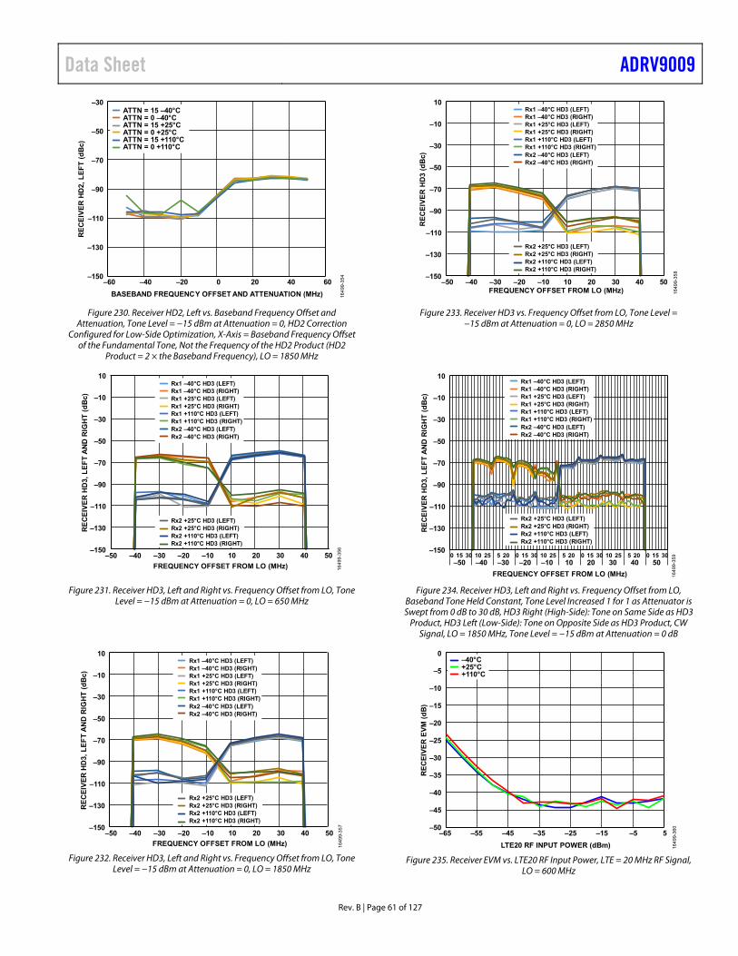
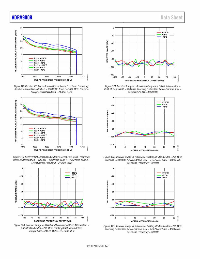
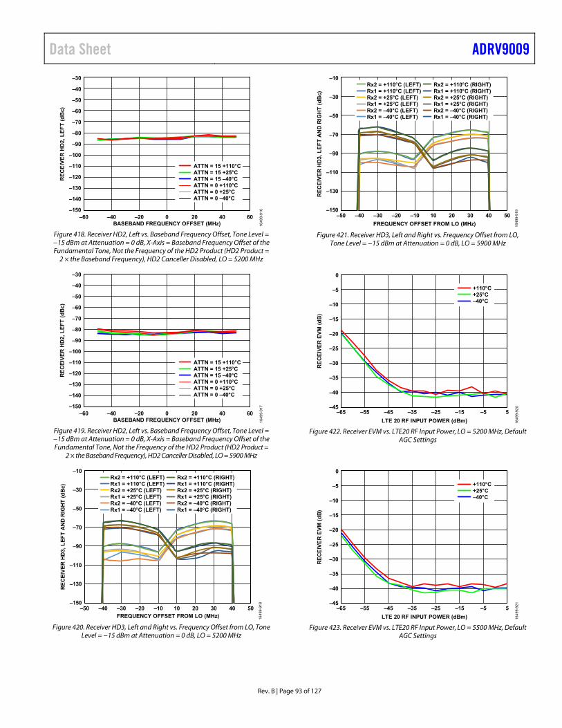
TERMINOLOGY Large Signal Bandwidth Large signal bandwidth, otherwise known as instantaneous bandwidth or signal bandwidth, is the bandwidth over which there are large signals. For example, for Band 42 LTE, the large signal bandwidth is 200 MHz.
Occupied Bandwidth Occupied bandwidth is the total bandwidth of the active signals. For example, three 20 MHz carriers have a 60 MHz occupied bandwidth, regardless of where the carriers are placed within the large signal bandwidth.
Synthesis Bandwidth Synthesis bandwidth is the bandwidth over which digital predistortion (DPD) linearization is transmitted. Synthesis bandwidth is the 1 dB bandwidth of the transmitter. The power density of the signal outside the occupied bandwidth is assumed to be 25 dB below the signal in the occupied bandwidth, which also assumes that the unlinearized power amplifier (PA) achieves 25 dB ACLR.
Observation Bandwidth Observation bandwidth is the 1 dB bandwidth of the observation receiver. With the observation receiver sharing the transmitter LO, the observation receiver senses similar power densities, such as those in the occupied bandwidth and synthesis bandwidth of the transmitter.
Backoff Backoff is the difference (in dB) between full scale and the rms signal power.
PHIGH PHIGH is the largest signal that can be applied without overloading the ADC for the receiver or observation receiver input. This input level results in slightly less than full scale at the digital output because of the nature of the continuous time Σ-Δ ADCs, which, for example, exhibit a soft overload in contrast to the hard clipping of pipeline ADCs.
ADRV9009 Data Sheet
Rev. B | Page 98 of 127
THEORY OF OPERATION The ADRV9009 is a highly integrated RF transmitter subsystem capable of configuration for a wide range of applications. The device integrates all RF, mixed-signal, and digital blocks necessary to provide all transmitter traffic and DPD observation receiver functions in a single device. Programmability allows the transmitter to be adapted for use in many TDD systems and 3G/4G/5G cellular standards. The ADRV9009 contains four high speed serial interface links for the transmitter chain, and two high speed links each for the receiver and observation receiver chains. The links are JESD204B, Subclass 1 compliant. The two receiver lanes can be reused for the observation receiver, providing a low pin count and a reliable data interface to field programmable gate arrays (FPGAs) or integrated baseband solutions.
The ADRV9009 also provides tracking correction of dc offset QEC errors and transmitter LO leakage to maintain high performance under varying temperatures and input signal conditions. The device also includes test modes that allow system designers to debug designs during prototyping and to optimize radio configurations.
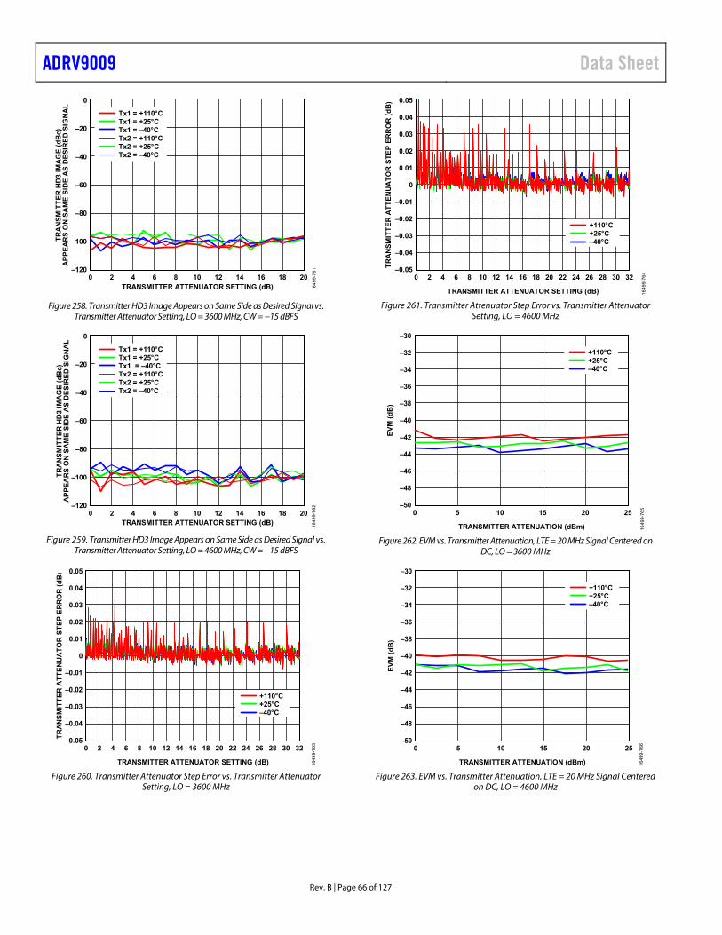
TRANSMITTER The ADRV9009 transmitter section consists of two identical and independently controlled channels that provide all digital processing, mixed-signal, and RF blocks necessary to implement a direct conversion system while sharing a common frequency synthesizer. The digital data from the JESD204B lanes pass through a fully programmable, 128-tap FIR filter with variable interpolation rates. The FIR output is sent to a series of interpolation filters that provide additional filtering and interpolation prior to reaching the DAC. Each 14-bit DAC has an adjustable sample rate.
When converted to baseband analog signals, the inphase (I) and quadrature (Q) signals are filtered to remove sampling artifacts and are fed to the upconversion mixers. Each transmitter chain provides a wide attenuation adjustment range with fine granularity to optimize SNR.
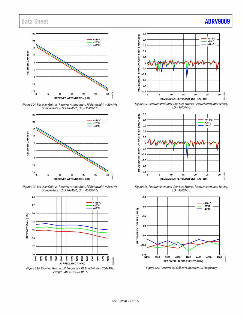
RECEIVER The ADRV9009 receiver contains all the blocks necessary to receive RF signals and convert them to digital data usable by a BBP. Each receiver can be configured as a direct conversion system that supports up to a 200 MHz bandwidth. Each receiver contains a programmable attenuator stage, followed by matched I and Q mixers that downconvert received signals to baseband for digitization.
Gain control can be achieved by using the on-chip AGC or by allowing the BBP to make gain adjustments in a manual gain control mode. Performance is optimized by mapping each gain control setting to specific attenuation levels at each adjustable gain block in the receiver signal path. Additionally, each channel contains independent receive signal strength indicator (RSSI) measurement capability, dc offset tracking, and all circuitry necessary for self calibration.
The receivers include ADCs and adjustable sample rates that produce data streams from the received signals. The signals can be conditioned further by a series of decimation filters and a programmable FIR filter with additional decimation settings. The sample rate of each digital filter block is adjustable by changing decimation factors to produce the desired output data rate.
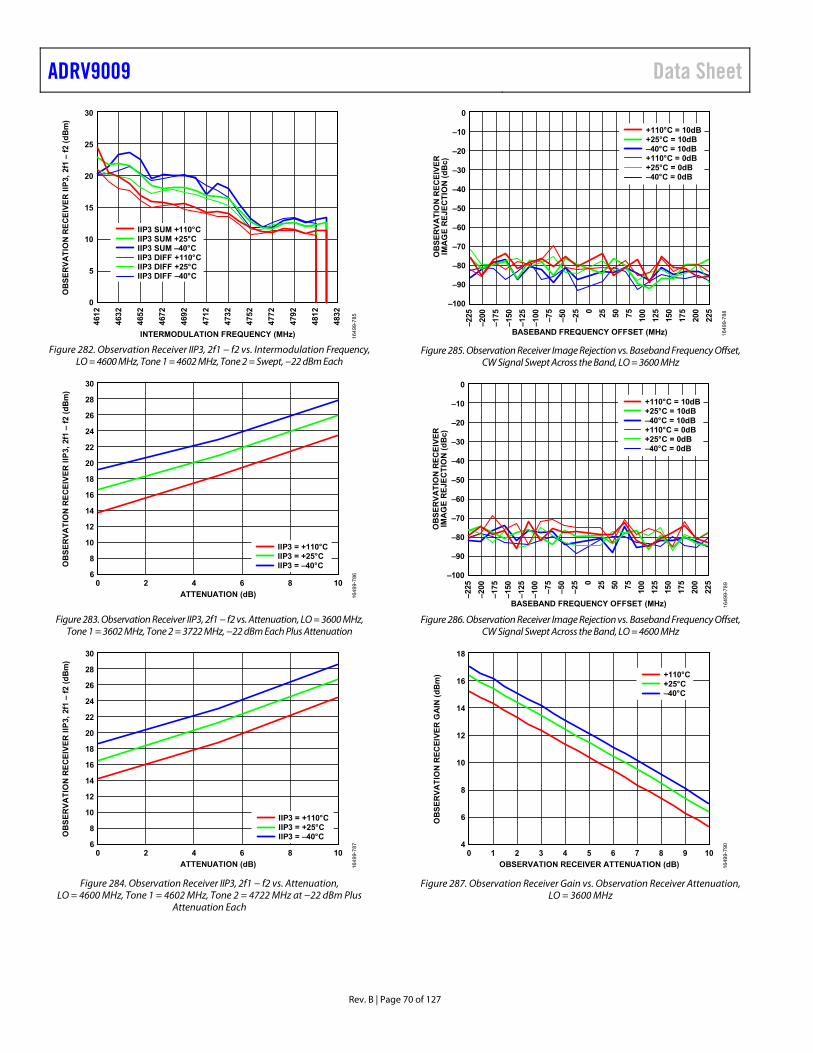
OBSERVATION RECEIVER The ADRV9009 contains an independent DPD observation receiver front end with two multiplexed inputs and a common digital back end that is shared with the traffic receiver. This configuration enables an efficient shared receiver and observation receiver mode where the device can support fast switching between receiver and observation receiver mode in TDD applications. The observation receiver shares the common frequency synthesizer with the transmitter.
The observation receiver is a direct conversion system that contains a programmable attenuator stage, followed by matched I and Q mixers, baseband filters, and ADCs.
The continuous time Σ-Δ ADCs have inherent antialiasing that reduces the RF filtering requirement.
The ADC outputs can be conditioned further by a series of decimation filters and a programmable FIR filter with additional decimation settings. The sample rate of each digital filter block is adjustable by changing decimation factors to produce the desired output data rate.
CLOCK INPUT The ADRV9009 requires a differential clock connected to the REF_CLK_IN± pins. The frequency of the clock input must be between 10 MHz and 1000 MHz and must have very low phase noise because this signal generates the RF LO and internal sampling clocks.
SYNTHESIZERS RF PLL
The ADRV9009 contains a fractional-N PLL to generate the RF LO for the signal paths. The PLL incorporates an internal VCO and loop filter, requiring no external components. The LOs on multiple chips can be phase synchronized to support active antenna systems and beamforming applications.
Clock PLL
The ADRV9009 contains a PLL synthesizer that generates all the baseband related clock signals and serialization/deserial-ization (SERDES) clocks. This PLL is programmed based on the data rate and sample rate requirements of the system.
Data Sheet ADRV9009
Rev. B | Page 99 of 127
SPI The ADRV9009 uses an SPI interface to communicate with the BBP. This interface can be configured as a 4-wire interface with dedicated receiver and transmitter ports, or the interface can be configured as a 3-wire interface with a bidirectional data communications port. This bus allows the BBP to set all device control parameters using a simple address data serial bus protocol.
Write commands follow a 24-bit format. The first five bits set the bus direction and the number of bytes to transfer. The next 11 bits set the address where data is written. The final 8 bits are the data to be transferred to the specific register address.
Read commands follow a similar format with the exception that the first 16 bits are transferred on the SDIO pin and the final eight bits are read from the ADRV9009, either on the SDO pin in 4-wire mode or on the SDIO pin in 3-wire mode.
JTAG BOUNDARY SCAN The ADRV9009 provides support for JTAG boundary scan. Five dual function pins are associated with the JTAG interface. Use these pins, listed in Table 5, to access the on-chip test access port. To enable the JTAG functionality, set the GPIO_3 pin through the GPIO_0 pin to 1001, and then pull the TEST pin high.
POWER SUPPLY SEQUENCE The ADRV9009 requires a specific power-up sequence to avoid undesired power-up currents. In the optimal power-up sequence, the VDDD1P3_DIG and the VDDA1P3 supplies (VDDA1P3 includes all 1.3 V domains) power up first and at the same time. If these supplies cannot be powered up simultaneously, the VDDD1P3_DIG supply must power up first. Power up the VDDA_3P3, VDDA1P8_BB, VDDA1P8_TX, VDDA1P3_DES, and VDDA1P3_SER supplies after the 1.3 V supplies. The VDD_INTERFACE supply can be powered up at any time. Note that no device damage occurs if this sequence is not followed. However, failure to follow this sequence may result in higher than expected power-up currents. It is also recommended to toggle the RESET signal after power stabilizes, prior to configuration. The power-down sequence is not critical. If a power-down sequence is followed, remove the VDDD1P3_DIG supply last to avoid any back biasing of the digital control lines.
GPIO_x PINS The ADRV9009 provides 19, 1.8 V to 2.5 V GPIO signals that can be configured for numerous functions. When configured as outputs, certain pins can provide real-time signal information to the BBP, allowing the BBP to determine observation receiver
performance. A pointer register selects the information that is output to these pins. Signals used for manual gain mode, calibration flags, state machine states, and various observation receiver parameters are among the outputs that can be monitored on these pins. Additionally, certain pins can be configured as inputs and used for various functions, such as setting the observation receiver gain in real time.
Twelve 3.3 V GPIO_x pins are also included on the device. These pins provide control signals to external components.
AUXILIARY CONVERTERS AUXADC_x
The ADRV9009 contains an auxiliary ADC that is multiplexed to four input pins (AUXADC_x). The auxiliary ADC is 12 bits with an input voltage range of 0.05 V to VDDA_3P3 − 0.05 V. When enabled, the auxiliary ADC is free running. The SPI reads provide the last value latched at the ADC output. The auxiliary ADC can also be multiplexed to a built in, diode-based temperature sensor.
Auxiliary DAC x
The ADRV9009 contains 10 identical auxiliary DACs (auxiliary DAC x) that can be used for bias or other system functionality. The auxiliary DACs are 10 bits, have an output voltage range of approximately 0.7 V to VDDA_3P3 − 0.3 V, and have an output drive of 10 mA.
JESD204B DATA INTERFACE The digital data interface for the ADRV9009 uses JEDEC JESD204B Subclass 1. The serial interface operates at speeds of up to 12.288 Gbps. The benefits of the JESD204B interface include a reduction in required board area for data interface routing, resulting in smaller total system size. Four high speed serial lanes are provided for the transmitter and four high speed lanes are provided for the observation receiver. The ADRV9009 supports single-lane or dual-lane interfaces as well as fixed and floating point data formats for observation receiver data.
Table 6. Observation Path Interface Rates
Bandwidth (MHz)
Output Rate (MSPS)
JESD204B Lane Rate (Mbps)
Number of Lanes
200 245.76 9830.4 1 200 307.2 12288 1 250 307.2 12288 1 450 491.52 9830.4 2 450 491.52 4915.2 4
ADRV9009 Data Sheet
Rev. B | Page 100 of 127
Table 7. Example Transmitter Interface Rates (Other Input Rates, Bandwidth, and JESD204B Lanes Also Supported)
Bandwidth (MHz)
Input Rate (MSPS)
Single-Channel Operation Dual-Channel Operation JESD204B Lane Rate (Mbps)
JESD204B Number of Lanes
JESD204B Lane Rate (Mbps)
JESD204B Number of Lanes
200 245.76 9830.4 1 9830.4 2 200 307.2 12288 1 12288 2 250 307.2 12288 1 12288 2 450 491.52 9830.4 2 9830.4 4
I/Q DAC
TRANSMITHALF-BAND
FILTER 2(INTERPOLATION
FACTOR 1, 2)
TRANSMITHALF-BAND
FILTER 1(INTERPOLATION
FACTOR 1, 2)
TRANSMIT FIRFILTER
(INTERPOLATIONFACTOR 1, 2, 4)
QUADRATURECORRECTION
DIGITALGAIN JESD204B
1649
9-3
09
Figure 430. Transmitter Datapath Filter Implementation
Table 8. Example Receiver Interface Rates (Other Output Rates, Bandwidth, and JESD204B Lanes Also Supported)
Bandwidth (MHz)
Output Rate (MSPS)
Single-Channel Operation Dual-Channel Operation JESD204B Lane Rate (Mbps)
JESD204B Number of Lanes
JESD204B Lane Rate (Mbps)
JESD204B Number of Lanes
80 122.88 4915.2 1 9830.4 1 100 153.6 6144 1 12288 1 100 245.76 9830.4 1 9830.4 2 200 245.76 9830.4 1 9830.4 2 200 245.76 4915.2 2 4915.2 4
RECEIVEHALF-BAND
FILTER3
ADC
RECEIVEHALF-BAND
FILTER2
RECEIVEHALF-BAND
FILTER1
FIRFILTER
(DECIMATIONFACTOR 1, 2, 4)
DCESTIMATION
DIGITALGAIN JESD204B
16
49
9-3
10
Figure 431. Receiver and Observation Receiver Datapath Filter Implementation
Data Sheet ADRV9009
Rev. B | Page 101 of 127
APPLICATIONS INFORMATION PCB LAYOUT AND POWER SUPPLY RECOMMENDATIONS Overview
The ADRV9009 device is a highly integrated RF agile transceiver with significant signal conditioning integrated on one chip. Due to the increased complexity of the device and its high pin count, careful PCB layout is important to get the optimal performance. This data sheet provides a checklist of issues to look for and guidelines on how to optimize the PCB to mitigate performance issues. The goal of this data sheet is to help achieve the optimal performance from the ADRV9009 while reducing board layout effort. This data sheet assumes that the user is an experienced analog and RF engineer with an understanding of RF PCB layout and RF transmission lines. This data sheet discusses the following issues and provides guidelines for system designers to achieve the optimal performance for the ADRV9009:
PCB material and stack up selection Fanout and trace space layout guidelines Component placement and routing guidelines RF and JESD204B transmission line layout Isolation techniques used on the ADRV9009-W/PCBZ Power management considerations Unused pin instructions
PCB MATERIAL AND STACKUP SELECTION Figure 432 shows the PCB stackup used for the ADRV9009-W/PCBZ. Table 9 and Table 10 list the single-ended and differential impedance for the stackup shown in Figure 432. The dielectric material used on the top and the bottom layers is 8 mil Rogers 4003C. The remaining dielectric layers are FR4-370 HR. The board design uses the Rogers laminate for the top layer and bottom layer for the low loss tangent at high frequencies. The ground planes under the Rogers laminate (Layer 2 and Layer 13) are the reference planes for the transmission lines routed on the outer surfaces. These layers are solid copper planes without any splits under the RF traces.
Layer 2 and Layer 13 are crucial to maintaining the RF signal integrity and, ultimately, the ADRV9009 performance. Layer 3 and Layer 12 route power supply domains. To keep the RF section of the ADRV9009 isolated from the fast transients of the digital section, the JESD204B interface lines are routed on Layer 5 and Layer 10. These layers have impedance control set to a 100 Ω differential. The remaining digital lines from the ADRV9009 are routed on Inner Layer 7 and Inner Layer 8. RF traces on the outer layers must be a controlled impedance to get the best performance from the device. The inner layers on this board use 0.5 ounce copper or 1 ounce copper. The outer layers use 1.5 ounce copper so the RF traces are less prone to pealing. Ground planes on this board are full copper floods with no splits except for vias, through-hole components, and isolation structures. The ground planes must route entirely to the edge of the PCB under the Surface-Mount Type A (SMA) connectors to maintain signal launch integrity. Power planes can be pulled back from the board edge to decrease the risk of shorting from the board edge.
1649
9-4
34
Figure 432. ADRV9009-W/PCBZ Trace Impedance and Stackup
ADRV9009 Data Sheet
Rev. B | Page 102 of 127
Table 9. ADRV9009-W/PCBZ Single Ended Impedance and Stackup1
Layer
Board Copper %
Starting Copper (oz.)
Finished Copper (oz.)
Single-Ended Impedance
Designed Trace Single-Ended (Inches)
Finished Trace Single-Ended (Inches)
Calculated Impedance (Ω)
Single-Ended Reference Layers
1 N/A 0.5 1.71 50 Ω ±10% 0.0155 0.0135 49.97 2 2 65 1 1 N/A N/A N/A N/A N/A 3 50 0.5 1 N/A N/A N/A N/A N/A 4 65 1 1 N/A N/A N/A N/A N/A 5 50 0.5 0.5 50 Ω ±10% 0.0045 0.0042 49.79 4, 6 6 65 1 1 N/A N/A N/A N/A N/A 7 50 0.5 0.5 50 Ω ±10% 0.0049 0.0039 50.05 6, 9 8 50 0.5 0.5 50 Ω ±10% 0.0049 0.0039 50.05 6, 9 9 65 1 1 N/A N/A N/A N/A N/A 10 50 0.5 1 50 Ω ±10% 0.0045 0.0039 49.88 9, 11 11 65 0.5 1 N/A N/A N/A N/A N/A 12 50 1 1 N/A N/A N/A N/A N/A 13 65 1 1 N/A N/A N/A N/A N/A 14 N/A 0.5 1.64 50 Ω ±10% 0.0155 0.0135 49.97 13 1 N/A means not applicable.
Table 10. ADRV9009-W/PCBZ Differential Impedance and Stackup1
Layer Differential Impedance
Designed Trace Differential (Inches)
Designed Gap Differential (Inches)
Finished Trace (Inches)
Finished Gap Differential (Inches)
Calculated Impedance (Ω)
Differential Reference Layers
1 100 Ω ±10% 0.008 0.006 0.007 0.007 99.55 2 50 Ω ±10% 0.0032 0.004 0.0304 0.0056 50.11 2 2 N/A N/A N/A N/A N/A N/A N/A 3 N/A N/A N/A N/A N/A N/A N/A 4 N/A N/A N/A N/A N/A N/A N/A 5 100 Ω ±10% 0.0036 0.0064 0.0034 0.0065 99.95 4, 6 6 N/A N/A N/A N/A N/A N/A N/A 7 100 Ω ±10% 0.0036 0.0064 0.0034 0.0066 100.51 6, 9 8 100 Ω ±10% 0.0038 0.0062 0.0034 0.0066 100.51 6, 9 9 N/A N/A N/A N/A N/A N/A N/A 10 100 Ω ±10% 0.0036 0.0064 0.003 0.007 100.80 9, 11 N/A N/A N/A N/A N/A N/A N/A N/A N/A N/A N/A N/A N/A N/A 11 N/A N/A N/A N/A N/A N/A N/A 12 N/A N/A N/A N/A N/A N/A N/A 13 100 Ω ±10% 0.008 0.006 0.007 0.007 99.55 13 14 50 Ω ±10% 0.032 N/A 0.004 N/A 50.11 13 1 N/A means not applicable.
Data Sheet ADRV9009
Rev. B | Page 103 of 127
FANOUT AND TRACE SPACE GUIDELINES The ADRV9009 uses a 196-ball chip scale package ball grid array (CSP_BGA), 12 mm × 12 mm package. The pitch between the pins is 0.8 mm. This small pitch makes it impractical to route all signals on a single layer. RF pins are placed on the outer edges of the ADRV9009 package. The location of the pins helps route the critical signals without a fanout via. Each digital signal is routed from the CSP_BGA pad using a 4.5 mil trace. The trace is connected to the CSP_BGA using a via in the pad structure. The signals are buried in the inner layers of the board for routing to other parts of the system.
The JESD204B interface signals are routed on two signal layers that use impedance control (Layer 5 and Layer 10). The spacing between the CSP_BGA pads is 17.5 mil. After the signal is on the inner layers, a 3.6 mil trace (50 Ω) connects the JESD204B signal to the FPGA mezzanine card (FMC) connector. The recommended CSP_BGA land pad size is 15 mil.
Figure 433 shows the fanout scheme of the ADRV9009-W/PCBZ. Like the CSP_BGA, the ADRV9009-W/PCBZ uses a via in the pad technique. This routing approach can be used for the ADRV9009 if there are no issues with manufacturing capabilities.
JESD INTERFACETRACE WIDTH = 3.6mil
4.5mil TRACE
AIR GAP = 17.5mil
PAD SIZE = 15mil
VIA SIZE = 14mil
16
49
9-4
35
Figure 433. Trace Fanout Scheme on the ADRV9009-W/PCBZ (PCB Layer Top and Layer 5 Enabled)
ADRV9009 Data Sheet
Rev. B | Page 104 of 127
COMPONENT PLACEMENT AND ROUTING GUIDELINES The ADRV9009 transceiver requires few external components to function, but those that are used require careful placement and routing to optimize performance. This section provides a checklist for properly placing and routing critical signals and components.
Signals with Highest Routing Priority
RF lines and JESD204B interface signals are the signals that are most critical and must be routed with the highest priority.
Figure 434 shows the general directions in which each of the signals must be routed so that they can be properly isolated from noisy signals.
The observation receiver and transmitter baluns and the matching circuits affect the overall RF performance of the
ADRV9009 transceiver. Make every effort to optimize the component selection and placement to avoid performance degradation. The RF Routing Guidelines section describes proper matching circuit placement and routing in more detail. Refer to the RF Port Interface Information section for more information.
To achieve the desired level of isolation between RF signal paths, use the technique described in the Isolation Techniques Used on the ADRV9009-W/PCBZ section in customer designs.
Install a 10 μF capacitor near the transmitter balun(s) VDDA1P8_TX dc feed(s) for RF transmitter outputs. The capacitor acts as a reservoir for the transmitter supply current. The Transmitter Balun DC Feed Supplies section discusses more details about the transmitter output power supply configuration.
VSSA ORX2_IN+ ORX2_IN– VSSA VSSA VSSA VSSA VSSA VSSA VSSA VSSA ORX1_IN+ ORX1_IN– VSSA
VDDA1P3_RX_RF
VSSA VSSA VSSA VSSA VSSA RF_EXT_LO_I/O–
RF_EXT_LO_I/O+
VSSA VSSA VSSA VSSA VSSA VSSA
GPIO_3p3_0 GPIO_3p3_3 VDDA1P3_RX_TX
VSSAVDDA1P3_
RF_VCO_LDOVDDA1P3_
RF_VCO_LDO VDDA1P1_RF_VCO
VDDA1P3_RF_LO
VSSAVDDA1P3_AUX_VCO_
LDO
VSSA VDDA_3P3 GPIO_3p3_9 RBIAS
GPIO_3p3_1 GPIO_3p3_4 VSSA VSSA VSSA VSSA VSSA VSSA VSSA VDDA1P1_AUX_VCO
VSSA VSSA GPIO_3p3_8 GPIO_3p3_10
GPIO_3p3_2 GPIO_3p3_5 GPIO_3p3_6 VDDA1P8_BB VDDA1P3_BB VSSA REF_CLK_IN+ REF_CLK_IN– VSSA AUX_SYNTH_OUT
AUXADC_3 VDDA1P8_TX GPIO_3p3_7 GPIO_3p3_11
VSSA VSSA AUXADC_0 AUXADC_1 VSSA VSSA VSSA VSSA VSSA VSSA AUXADC_2 VSSA VSSA VSSA
VSSA VSSA VSSA VSSAVDDA1P3_
CLOCK_SYNTH
VSSAVDDA1P3_RF_SYNTH
VDDA1P3_AUX_SYNTH RF_SYNTH_
VTUNEVSSA VSSA VSSA VSSA VSSA
TX2_OUT– VSSA VSSA VSSA VSSA VSSA VSSA VSSA VSSA VSSA GPIO_12 GPIO_11 VSSA TX1_OUT+
TX2_OUT+ VSSA GPIO_18 RESET GP_INTERRUPT
TEST GPIO_2 GPIO_1 SDIO SDO GPIO_13 GPIO_10 VSSA TX1_OUT–
VSSA VSSA SYSREF_IN+ SYSREF_IN– GPIO_5 GPIO_4 GPIO_3 GPIO_0 SCLK CS GPIO_14 GPIO_9 VSSA VSSA
VSSA VSSA SYNCIN1– SYNCIN1+ GPIO_6 GPIO_7 VSSD VDDD1P3_DIG
VDDD1P3_DIG
VSSD GPIO_15 GPIO_8 SYNCOUT1– SYNCOUT1+
VDDA1P1_
CLOCK_VCOVSSA SYNCIN0– SYNCIN0+ ORX1_
ENABLETX1_
ENABLEORX2_
ENABLETX2_
ENABLEVSSA GPIO_17 GPIO_16 VDD_
INTERFACESYNCOUT0– SYNCOUT0+
VDDA1P3_CLOCK_
VCO_ LDO
VSSA SERDOUT3– SERDOUT3+ SERDOUT2– SERDOUT2+ VSSA VDDA1P3_SER
VDDA1P3_DES
SERDIN1– SERDIN1+ SERDIN0– SERDIN0+ VSSA
AUX_SYNTH_VTUNE
VSSA VSSA SERDOUT1– SERDOUT1+ SERDOUT0– SERDOUT0+ VDDA1P3_SER
VDDA1P3_DES
VSSA SERDIN3– SERDIN3+ SERDIN2– SERDIN2+
164
99-4
36
Figure 434. RF Input/Output, REF_CLK_IN±, and JESD204B Signal Routing Guidelines
Data Sheet ADRV9009
Rev. B | Page 105 of 127
Figure 435 shows placement for ac coupling capacitors and a 100 Ω termination resistor near the REF_CLK_IN± pins. Shield the traces with ground flooding that is surrounded with vias staggered along the edge of the trace pair. The trace pair creates a shielded channel that shields the reference clock from any interference from other signals. Refer to the ADRV9009-W/PCBZ layout, including board support files included with the evaluation board software, for exact details.
Route the JESD204B interface at the beginning of the PCB design and with the same priority as the RF signals. The RF Routing Guidelines section outlines recommendations for
JESD204B interface routing. Provide appropriate isolation between interface differential pairs. The Isolation Between JESD204B Lines section provides guidelines for optimizing isolation.
The RF_EXT_LO_I/O− pin (B7) and the RF_EXT_LO_I/O+ pin (B8) on the ADRV9009 are internally dc biased. If an external LO is used, connect the LO via ac coupling capacitors.
TO ADRV9009BGA BALLS
AC COUPLINGCAPS
100ΩTERMINATIONRESISTOR
16
49
9-4
39
Figure 435. REF_CLK_IN± Routing Recommendation
ADRV9009 Data Sheet
Rev. B | Page 106 of 127
Signals with Second Routing Priority
Power supply quality has a direct impact on overall system performance. To achieve optimal performance, follow recommendations regarding ADRV9009 power supply routing. The following recommendations outline how to route different power domains that can be connected together directly and that can be tied to the same supply, but are separated by a 0 Ω placeholder resistor or ferrite bead (FB).
When using a trace to connect power to a particular domain, ensure that this trace is surrounded by ground.
Figure 436 shows an example of such traces routed on Layer 12 of the ADRV9009-W/PCBZ. Each trace is separated from any other signal by the ground plane and vias. Separating the traces from other signals is essential to providing necessary isolation between the ADRV9009 power domains.
16
49
9-4
40
Figure 436. Layout Example of Power Supply Domains Routed with Ground Shielding (Layer 12 to Power)
Data Sheet ADRV9009
Rev. B | Page 107 of 127
Each power supply pin requires a 0.1 μF bypass capacitor near the pin at a minimum. Place the ground side of the bypass capacitor in a way so that ground currents flow away from other power pins and the bypass capacitors.
For the domains shown in Figure 437, like the domains powered through a 0 Ω placeholder resistor or FB, place the 0 Ω placeholder resistors or FBs further away from the device. Space 0 Ω placeholder resistors or FBs apart from each other to ensure that the electric fields on the FBs do not influence each other. Figure 438 shows an example of how the FBs, reservoir capacitors, and decoupling capacitors are placed. It is
recommended to connect an FB between a power plane and the ADRV9009 at a distance away from the device (see Figure 438 for specific distances) The FB and the reservoir capacitor provide stable voltage for the ADRV9009 during operation by isolating the pin or pins that the network is connected to from the power plane. Then, shield that trace with ground and provide power to the power pins on the ADRV9009. Place a 100 nF capacitor near the power supply pin with the ground side of the bypass capacitor placed in a way so that ground currents flow away from other power pins and the bypass capacitors.
VSSA ORX2_IN+ ORX2_IN– VSSA VSSA VSSA VSSA VSSA VSSA VSSA VSSA ORX1_IN+ ORX1_IN– VSSA
VDDA1P3_RX_RF
VSSA VSSA VSSA VSSA VSSA RF_EXT_LO_I/O–
RF_EXT_LO_I/O+
VSSA VSSA VSSA VSSA VSSA VSSA
GPIO_3p3_0 GPIO_3p3_3 VDDA1P3_RX_TX
VSSAVDDA1P3_
RF_VCO_LDOVDDA1P3_
RF_VCO_LDO VDDA1P1_RF_VCO
VDDA1P3_RF_LO
VSSAVDDA1P3_AUX_VCO_
LDO
VSSA VDDA_3P3 GPIO_3p3_9 RBIAS
GPIO_3p3_1 GPIO_3p3_4 VSSA VSSA VSSA VSSA VSSA VSSA VSSA VDDA1P1_AUX_VCO
VSSA VSSA GPIO_3p3_8 GPIO_3p3_10
GPIO_3p3_2 GPIO_3p3_5 GPIO_3p3_6 VDDA1P8_BB VDDA1P3_BB VSSA REF_CLK_IN+ REF_CLK_IN– VSSA AUX_SYNTH_OUT
AUXADC_3 VDDA1P8_TX GPIO_3p3_7 GPIO_3p3_11
VSSA VSSA AUXADC_0 AUXADC_1 VSSA VSSA VSSA VSSA VSSA VSSA AUXADC_2 VSSA VSSA VSSA
VSSA VSSA VSSA VSSAVDDA1P3_
CLOCK_SYNTH
VSSAVDDA1P3_RF_SYNTH
VDDA1P3_AUX_SYNTH RF_SYNTH_
VTUNEVSSA VSSA VSSA VSSA VSSA
TX2_OUT– VSSA VSSA VSSA VSSA VSSA VSSA VSSA VSSA VSSA GPIO_12 GPIO_11 VSSA TX1_OUT+
TX2_OUT+ VSSA GPIO_18 RESET GP_INTERRUPT
TEST GPIO_2 GPIO_1 SDIO SDO GPIO_13 GPIO_10 VSSA TX1_OUT–
VSSA VSSA SYSREF_IN+ SYSREF_IN– GPIO_5 GPIO_4 GPIO_3 GPIO_0 SCLK CS GPIO_14 GPIO_9 VSSA VSSA
VSSA VSSA SYNCIN1– SYNCIN1+ GPIO_6 GPIO_7 VSSD VDDD1P3_DIG
VDDD1P3_DIG
VSSD GPIO_15 GPIO_8 SYNCOUT1– SYNCOUT1+
VDDA1P1_
CLOCK_VCOVSSA SYNCIN0– SYNCIN0+ ORX1_
ENABLETX1_
ENABLEORX2_
ENABLETX2_
ENABLEVSSA GPIO_17 GPIO_16 VDD_
INTERFACESYNCOUT0– SYNCOUT0+
VDDA1P3_CLOCK_
VCO_ LDO
VSSA SERDOUT3– SERDOUT3+ SERDOUT2– SERDOUT2+ VSSA VDDA1P3_SER
VDDA1P3_DES
SERDIN1– SERDIN1+ SERDIN0– SERDIN0+ VSSA
AUX_SYNTH_VTUNE
VSSA VSSA SERDOUT1– SERDOUT1+ SERDOUT0– SERDOUT0+ VDDA1P3_SER
VDDA1P3_DES
VSSA SERDIN3– SERDIN3+ SERDIN2– SERDIN2+
TRACE THROUGH 0.1Ω RESISTOR TO AP
TRACE THROUGH 0Ω TO AP
TRACE THROUGH0Ω TO AP
TRACE THROUGH0Ω TO 1.8V PLANE
TRACE THROUGH0Ω TO AP
TRACE THROUGH1Ω RESISTOR TO AP
TRACE THROUGH0Ω TO AP
TRACE THROUGH 0Ω RES. TO 1.3V ANALOG PLANE (AP)MAINTAIN LOWEST POSSIBLE IMPEDANCE
TRACE THROUGH FBTO 3.3V PLANE
TRACE THROUGH0Ω TO 1.8V PLANE
TRACE THROUGHFB TO INTERFACE SUPPLY
TRACE THROUGH 0ΩTO 1.3V JESD204B SUPPLY
TRACE THROUGH FBTO 1.3V JESD204B SUPPLY
TRACE THROUGH0Ω TO AP
WIDE TRACE TO1.3V DIGITAL SUPPLYHIGH CURRENT
1649
9-4
41
Figure 437. Power Supply Domains Interconnection Guidelines
ADRV9009 Data Sheet
Rev. B | Page 108 of 127
DUT
0Ω RESISTOR
1µ + 100nF bypass
CAPS ORIENTED SUCH
THAT CURRENTS FLOW
AWAY FROM OTHER
POWER PINS
PLACEHOLDERS
FOR FERRITE BEADS
0Ω RESISTOR
PLACEHOLDERS
FOR FERRITE BEADS
RESERVOIRCAPACITORS
1649
9-4
44
Figure 438. Placement Example of 0 Ω Resistor Placeholders for FBs, Reservoir Capacitors, and Bypass Capacitors on the ADRV9009-W/PCBZ (Layer 12 to Power Layer and
Bottom Layer)
Data Sheet ADRV9009
Rev. B | Page 109 of 127
Signals with Lowest Routing Priority
As a last step while designing the PCB layout, route signals shown in Figure 439. The following list outlines the recommended order of signal routing:
1. Use ceramic 1 μF bypass capacitors at the VDDA1P1_ RF_VCO pin, VDDA1P1_AUX_VCO pin, and VDDA1P1_CLOCK_VCO pin. Place them as close as possible to the ADRV9009 device with the ground side of the bypass capacitor placed in a way so that ground currents flow away from other power pins and the bypass capacitors, if possible.
2. Connect a 14.3 kΩ resistor to the RBIAS pin (C14). This resistor must have a 1% tolerance.
3. Pull the TEST pin (J6) to ground for normal operation. The device has support for JTAG boundary scan, and this pin is used to access that function. Refer to the JTAG Boundary Scan section for JTAG boundary scan information.
4. Pull the RESET pin (J4) high with a 10 kΩ resistor to VDD_ INTERFACE for normal operation. To reset the device, drive the RESET pin low.
When routing analog signals, such as GPIO_3P3_x/Auxiliary DAC x or AUXADC_x, it is recommended to route them away from the digital section (Row H through Row P). Do not cross the analog section of the ADRV9009, highlighted by a red dotted line in Figure 439, by any digital signal routing.
When routing digital signals from Row H and below, it is important to route them away from the analog section (Row A through Row G). Do not cross the analog section of the ADRV9009, highlighted by a red dotted line in Figure 439, by any digital signal routing.
VSSA ORX2_IN+ ORX2_IN– VSSA VSSA VSSA VSSA VSSA VSSA VSSA VSSA ORX1_IN+ ORX1_IN– VSSA
VDDA1P3_RX_RF
VSSA VSSA VSSA VSSA VSSA RF_EXT_LO_I/O–
RF_EXT_LO_I/O+
VSSA VSSA VSSA VSSA VSSA VSSA
GPIO_3p3_0 GPIO_3p3_3 VDDA1P3_RX_TX
VSSAVDDA1P3_
RF_VCO_LDOVDDA1P3_
RF_VCO_LDO VDDA1P1_RF_VCO
VDDA1P3_RF_LO
VSSAVDDA1P3_AUX_VCO_
LDO
VSSA VDDA_3P3 GPIO_3p3_9 RBIAS
GPIO_3p3_1 GPIO_3p3_4 VSSA VSSA VSSA VSSA VSSA VSSA VSSA VDDA1P1_AUX_VCO
VSSA VSSA GPIO_3p3_8 GPIO_3p3_10
GPIO_3p3_2 GPIO_3p3_5 GPIO_3p3_6 VDDA1P8_BB VDDA1P3_BB VSSA REF_CLK_IN+ REF_CLK_IN– VSSA AUX_SYNTH_OUT
AUXADC_3 VDDA1P8_TX GPIO_3p3_7 GPIO_3p3_11
VSSA VSSA AUXADC_0 AUXADC_1 VSSA VSSA VSSA VSSA VSSA VSSA AUXADC_2 VSSA VSSA VSSA
VSSA VSSA VSSA VSSAVDDA1P3_
CLOCK_SYNTH
VSSAVDDA1P3_RF_SYNTH
VDDA1P3_AUX_SYNTH RF_SYNTH_
VTUNEVSSA VSSA VSSA VSSA VSSA
TX2_OUT– VSSA VSSA VSSA VSSA VSSA VSSA VSSA VSSA VSSA GPIO_12 GPIO_11 VSSA TX1_OUT+
TX2_OUT+ VSSA GPIO_18 RESET GP_INTERRUPT
TEST GPIO_2 GPIO_1 SDIO SDO GPIO_13 GPIO_10 VSSA TX1_OUT–
VSSA VSSA SYSREF_IN+ SYSREF_IN– GPIO_5 GPIO_4 GPIO_3 GPIO_0 SCLK CS GPIO_14 GPIO_9 VSSA VSSA
VSSA VSSA SYNCIN1– SYNCIN1+ GPIO_6 GPIO_7 VSSD VDDD1P3_DIG
VDDD1P3_DIG
VSSD GPIO_15 GPIO_8 SYNCOUT1– SYNCOUT1+
VDDA1P1_
CLOCK_VCOVSSA SYNCIN0– SYNCIN0+ ORX1_
ENABLETX1_
ENABLEORX2_
ENABLETX2_
ENABLEVSSA GPIO_17 GPIO_16 VDD_
INTERFACESYNCOUT0– SYNCOUT0+
VDDA1P3_CLOCK_
VCO_ LDO
VSSA SERDOUT3– SERDOUT3+ SERDOUT2– SERDOUT2+ VSSA VDDA1P3_SER
VDDA1P3_DES
SERDIN1– SERDIN1+ SERDIN0– SERDIN0+ VSSA
AUX_SYNTH_VTUNE
VSSA VSSA SERDOUT1– SERDOUT1+ SERDOUT0– SERDOUT0+ VDDA1P3_SER
VDDA1P3_DES
VSSA SERDIN3– SERDIN3+ SERDIN2– SERDIN2+
1µF CAPACITOR
14.3kΩ RESISTOR
ALL DIGITALGPIO SIGNALSROUTED BELOWTHE RED LINE
1µF CAPACITOR
1µF CAPACITOR
164
99-4
45
Figure 439. Auxiliary ADC, Analog, and Digital GPIO Signals Routing Guidelines
ADRV9009 Data Sheet
Rev. B | Page 110 of 127
RF AND JESD204B TRANSMISSION LINE LAYOUT RF Routing Guidelines
The ADRV9009-W/PCBZ uses microstrip type lines for receiver, observation receiver, and transmitter RF traces. In general, it is not recommended to use any number of vias to route RF traces unless a direct line route is not possible. Differential lines from the balun to the receiver pins, observation receiver pins, and transmitter pins must be as short as possible. Also, make the length of the single-ended transmission line short to minimize the effects of parasitic coupling. These traces are the most critical when optimizing performance and are, therefore, routed before any other routing. These traces have the highest priority if trade-offs are needed.
Figure 440 and Figure 441 show pi matching networks on the single-ended side of the baluns. The observation receiver front
end is dc biased internally, so the differential side of the balun is ac-coupled. The system designer can optimize the RF performance with a proper selection of the balun, matching components, and ac coupling capacitors. The external LO traces and the REF_CLK_IN± traces may require matching components as well to ensure optimal performance.
All the RF signals mentioned previously must have a solid ground reference under each trace. Do not run any of the critical traces over a section of the reference plane that is discontinuous. The ground flood on the reference layer must extend all the way to the edge of the board. This flood length ensures signal integrity for the SMA launch when an edge launch connector is used.
Refer to the RF Port Interface Information section for more information on RF matching recommendations for the device.
164
99-4
48
Figure 440. Pi Network Matching Components Available on Transmitter and Receiver
Data Sheet ADRV9009
Rev. B | Page 111 of 127
16
49
9-4
49
Figure 441. Pi Network Matching Components Available on Observation Receiver Inputs
ADRV9009 Data Sheet
Rev. B | Page 112 of 127
Transmitter Balun DC Feed Supplies
Each transmitter requires approximately 200 mA supplied through an external connection. On the ADRV9008-2 and ADRV9009 evaluation boards, bias voltages are supplied at the dc feed of the baluns. Layout of both boards allows the use of external chokes to provide a 1.8 V power domain to the ADRV9009 outputs. This configuration is useful in scenarios where a balun used at the transmitter output is not capable of conducting the current necessary for the transmitter outputs to
operate. To reduce switching transients when attenuation settings change, power the balun dc feed or transmitter output chokes directly by the 1.8 V plane. Design the geometry of the 1.8 V plane so that each balun supply or each set of two chokes is isolated from the other. This geometry can affect transmitter to transmitter isolation. Figure 442 shows the layout configuration used on the ADRV9009-W/PCBZ.
Tx OUTPUT / BALUN1.8V SUPPLY FEED
1649
9-4
50
Figure 442. Transmitter Power Supply Planes (VDDA1P8_TX) on the ADRV9009-W/PCBZ
Data Sheet ADRV9009
Rev. B | Page 113 of 127
Both the positive and negative transmitter pins must be biased with 1.8 V. This biasing is accomplished on the evaluation board through chokes and decoupling capacitors, as shown in Figure 443. Match both chokes and their layout to avoid potential current spikes. A difference in parameters between both chokes can cause unwanted emission at transmitter outputs. Place the decoupling capacitors that are near the transmitter balun as close as possible to the dc feed of the balun or the ground pin. Make orientation of the capacitor perpendicular to the device so that the return current forms as small a loop as possible with the ground pins surrounding the transmitter input. A combination network of capacitors provides a wideband and low impedance ground path, eliminates transmitter spectrum spurs, and dampens the transients.
DC FEED
CHOKES
DECOUPLING
CAPACITORS
1.8V TX POWER
DOMAIN FEED
CONDUCTING
RESISTORSBALUN
BALUN
DECOUPLING
CAPACITORS
TALISE TX OUTPUT
16
49
9-4
51
ADRV9009 TX OUTPUT
Figure 443. Transmitter DC Chokes and Balun Feed Supply
JESD204B Trace Routing Recommendations
The ADRV9009 transceiver uses the JESD204B, high speed serial interface. To ensure optimal performance of this interface, keep the differential traces as short as possible by placing the ADRV9009 as close as possible to the FPGA or BBP, and route the traces directly between the devices. Use a PCB material with a low dielectric constant (<4) to minimize loss. For distances greater than 6 inches, use a premium PCB material such as RO4350B or RO4003C.
Routing Recommendations
Route the differential pairs on a single plane using a solid ground plane as a reference on the layers above and below these traces.
All JESD204B lane traces must be impedance controlled to achieve 50 Ω to ground. It is recommended that the differential pair be coplanar and loosely coupled. An example of a typical configuration is a 5 mil trace width and 15 mil edge to edge spacing, with the trace width maximized, as shown in Figure 444.
Match trace widths with pin and ball widths while maintaining impedance control. If possible, use 1 oz. copper trace widths of at least 8 mil (200 μm). The coupling capacitor pad size must match JESD204B lane trace widths. If the trace width does not match the pad size, use a smooth transition between different widths.
The pad area for all connector and passive component choices must be minimized due to a capacitive plate effect that leads to problems with signal integrity.
Reference planes for impedance controlled signals must not be segmented or broken for the entire length of a trace.
The REF_CLK_IN± signal trace and the SYSREF signal trace are impedance controlled for characteristic impedance (ZO) = 50 Ω.
Stripline Transmission Lines vs. Microstrip Transmission Lines
Stripline transmission lines have less signal loss and emit less electromagnetic interference than microstrip transmission lines. However, stripline transmission lines require the use of vias that add line inductance, increasing the difficulty of controlling the impedance.
Microstrip transmission lines are easier to implement if the component placement and density allow routing on the top layer. Microstrip transmission lines make controlling the impedance easier.
If the top layer of the PCB is used by other circuits or signals, or if the advantages of stripline transmission lines are more desirable than the advantages of microstrip transmission lines, implement the following recommendations:
Minimize the number of vias. Use blind vias where possible to eliminate via stub effects,
and use microvias to minimize via inductance. When using standard vias, use a maximum via length to
minimize the stub size. For example, on an 8-layer board, use Layer 7 for the stripline pair.
Place a pair of ground vias in proximity to each via pair to minimize the impedance discontinuity.
ADRV9009 Data Sheet
Rev. B | Page 114 of 127
Route the JESD204B lines on the top side of the evaluation board as a differential 100 Ω pair (microstrip). For the ADRV9009-W/PCBZ, the JESD204B differential signals are routed on the inner layers of the board (Layer 5 and Layer 10) as differential 100 Ω pairs (stripline). To minimize potential coupling, these signals are placed on an inner layer using a via embedded in the component footprint pad where the ball connects to the PCB. The ac coupling capacitors (100 nF) on these signals are placed near the connector and away from the chip to minimize coupling. The JESD204B interface can operate at frequencies of up to 12 GHz. Ensure that signal integrity from the chip to the connector is maintained.
ISOLATION TECHNIQUES USED ON THE ADRV9009-W/PCBZ Isolation Goals
Significant isolation challenges were overcome in designing the ADRV9009-W/PCBZ. The following isolation requirements accurately evaluate the ADRV9009 transceiver performance:
Transmitter to transmitter: 75 dB out to 6 GHz Transmitter to receiver: 65 dB out to 6 GHz Receiver to receiver: 65 dB out to 6 GHz Transmitter to observation receiver: 65 dB out to 6 GHz
To meet these isolation goals with significant margin, isolation structures are introduced.
Figure 445 shows the isolation structures used on the ADRV9009-W/PCBZ. These structures consist of a combination of slots and square apertures. These structures are present on every copper layer of the PCB stack. The advantage of using square apertures is that signals can be routed between the openings without affecting the isolation benefits of the array of apertures. When using these isolation structures, make sure to place ground vias around the slots and apertures.
TxDIFFERENTIAL A
TxDIFFERENTIAL B
TxDIFFERENTIAL A
TxDIFFERENTIAL B
TIGHTLY COUPLEDDIFFERENTIAL Tx LINES
LOOSELY COUPLEDDIFFERENTIAL Tx LINES 1
64
99-4
52
Figure 444. Routing JESD204B, Differential A and Differential B Correspond to Differential Positive Signals or Negative Signals (One Differential Pair)
16
499-
453
Figure 445. Isolation Structures on the ADRV9009-W/PCBZ
Data Sheet ADRV9009
Rev. B | Page 115 of 127
16
49
9-4
54
Figure 446. Current Steering Vias Placed Next to Isolation Structures
Figure 446 outlines the methodology used on the ADRV9009-W/PCBZ. When using slots, ground vias must be placed at the ends of the slots and along the sides of the slots. When using square apertures, at least one single ground via must be placed adjacent to each square. These vias must be through-hole vias from the top layer to the bottom layer. The function of these vias is to steer return current to the ground planes near the apertures.
For accurate slot spacing and square apertures layout, use simulation software when designing a PCB for the ADRV9009 transceiver. Spacing between square apertures must be no more than 1/10 of a wavelength.
Calculate the wavelength using Equation 1:
300( )
(MHz) R
Wavelength mFrequency E
(1)
where ER is the dielectric constant of the isolator material. For RO4003C material, microstrip structure (+ air), ER = 2.8. For FR4-370HR material, stripline structure, ER = 4.1.
For example, if the maximum RF signal frequency is 6 GHz, and ER = 2.8 for RO4003C material, microstrip structure (+ air), the minimum wavelength is approximately 29.8 mm.
To follow the 1/10 wavelength spacing rule, square aperture spacing must be 2.98 mm or less.
Isolation Between JESD204B Lines
The JESD204B interface uses eight line pairs that can operate at speeds of up to 12 GHz. When configuring the PCB layout, ensure that these lines are routed according to the rules outlined in the JESD204B Trace Routing Recommendations section. In addition,
use isolation techniques to prevent crosstalk between different JESD204B lane pairs.
Figure 447 shows a technique used on the ADRV9009-W/PCBZ that involves via fencing. Placing ground vias around each JESD204B pair provides isolation and decreases crosstalk. The spacing between vias is 1.24 mm.
Figure 447 shows the rule provided in Equation 1. JESD204B lines are routed on Layer 5 and Layer 10 so that the lines use stripline structures. The dielectric material used in the inner layers of the ADRV9009-W/PCBZ PCB is FR4-370HR.
For accurate spacing of the JESD204B fencing vias, use layout simulation software. Input the following data into Equation 1 to calculate the wavelength and square aperture spacing:
The maximum JESD204B signal frequency is approximately 12 GHz.
For FR4-370HR material, stripline structure, ER = 4.1, the minimum wavelength is approximately 12.4 mm.
To follow the 1/10 wavelength spacing rule, spacing between vias must be 1.24 mm or less. The minimum spacing recommendation according to transmission line theory is 1/4 wavelength.
ADRV9009 Data Sheet
Rev. B | Page 116 of 127
1.24mm
16
49
9-4
55
Figure 447. Via Fencing Around JESD204B Lines, PCB Layer 10
RF PORT INTERFACE INFORMATION This section details the RF transmitter and receiver interfaces for optimal device performance. This section also includes data for the ADRV9009 RF port impedance values (see Figure 448 and Figure 449 for impedance values) and examples of impedance matching networks used in the evaluation platform. This section also provides information on board layout techniques and balun selection guidelines.
The ADRV9009 is a highly integrated transceiver with transmit, receive, and observation (DPD) receive signal chains. External impedance matching networks are required on the transmitter and receiver ports to achieve the performance levels indicated in this data sheet.
It is recommended to use simulation tools in the design and optimization of impedance matching networks. To achieve the closest match between computer simulated results and measured results, accurate models of the board environment, surface-mount device (SMD) components (including baluns and filters), and ADRV9009 port impedances are required.
RF Port Impedance Data
This section provides the port impedance data for all transmitters and receivers in the ADRV9009 integrated transceiver. Note the following:
ZO is defined as 50 Ω. The ADRV9009 ball pads are the reference plane for this data. Single-ended mode port impedance data is not available.
However, a rough assessment is possible by taking the differential mode port impedance data and dividing both the real and imaginary components by 2.
Contact Analog Devices applications engineering for the impedance data in Touchstone format.
Data Sheet ADRV9009
Rev. B | Page 117 of 127
0
5.0
–5.0
2.0
1.0
–1.0
–2.0
0.5
–0.5
0.2
–0.2
m26FREQUENCY = 3GHzS(1,1) = 0.368/150.626IMPEDANCE = 24.355 + j10.153
m27FREQUENCY = 4GHzS(1,1) = 0.484/107.379IMPEDANCE = 25.118 + j30.329m28FREQUENCY = 5GHzS(1,1) = 0.569/70.352IMPEDANCE = 35.932 + j56.936m29FREQUENCY = 6GHzS(1,1) = 0.614/36.074IMPEDANCE = 81.032 + j94.014
m21FREQUENCY = 100MHzS(1,1) = 0.143/–7.865IMPEDANCE = 66.439 – j2.654
m22FREQUENCY = 300MHzS(1,1) = 0.141/–25.589IMPEDANCE = 64.063 – j7.987m23FREQUENCY = 500MHzS(1,1) = 0.145/–42.661IMPEDANCE = 60.623 – j12.201m24FREQUENCY = 1GHzS(1,1) = 0.164/–84.046IMPEDANCE = 49.000 + j16.447
m25FREQUENCY = 2GHzS(1,1) = 0.247/–155.186IMPEDANCE = 31.131 – j6.860
M29
M28M27
M26
M25M24 M23
M22M21
FREQUENCY (0.000Hz TO 6.000Hz)
S91
,1)
16499-458
Figure 448. Transmitter 1 and Transmitter 2 SEDZ and Parallel Equivalent Differential Impedance (PEDZ) Data
0
5.0
–5.0
2.0
1.0
–1.0
–2.0
0.5
–0.5
0.2
–0.2
m15FREQUENCY = 100MHzS(1,1) = 0.390/–1.819IMPEDANCE = 113.933 – j3.331
m16FREQUENCY = 300MHzS(1,1) = 0.390/–5.495IMPEDANCE = 112.803 – j9.931m17FREQUENCY = 500MHzS(1,1) = 0.388/–9.198IMPEDANCE = 110.398 – j16.107m18FREQUENCY = 1GHzS(1,1) = 0.377–18.643IMPEDANCE = 100.377 – j28.250
m19FREQUENCY = 2GHzS(1,1) = 0.336/–39.123IMPEDANCE = 74.966 – j35.800
FREQUENCY (0Hz TO 6GHz)
M21
M23
m20FREQUENCY = 3GHzS(1,1) = 0.267/–64.650IMPEDANCE = 55.102 – j28.685
m21FREQUENCY = 4GHzS(1,1) = 0.186/–104.336IMPEDANCE = 42.821 – j16.026m22FREQUENCY = 5GHzS(1,1) = 0.164/–173.106IMPEDANCE = 35.977 – j1.455m23FREQUENCY = 6GHzS(1,1) = 0.266/130.063IMPEDANCE = 32.890 + j14.399
S(1
,1)
M20
M19 M18
M17M16M15M22
16499-459
Figure 449. Receiver 1 and Receiver 2 SEDZ and PEDZ Data
ADRV9009 Data Sheet
Rev. B | Page 118 of 127
0
5.0
–5.0
2.0
1.0
–1.0
–2.0
0.5
–0.5
0.2
–0.2
m15FREQUENCY = 100MHzS(1,1) = 0.391/–1.848IMPEDANCE = 114.099 – j3.397
m16FREQUENCY = 300MHzS(1,1) = 0.389/–5.601IMPEDANCE = 112.639 – j10.091m17FREQUENCY = 500MHzS(1,1) = 0.385/–9.396IMPEDANCE = 109.556 – j16.156m18FREQUENCY = 1GHzS(1,1) = 0.362–19.087IMPEDANCE = 97.259 – j26.513
m19FREQUENCY = 2GHzS(1,1) = 0.267/–39.928IMPEDANCE = 70.789 – j25.940
M22
FREQUENCY (0Hz TO 6GHz)
M21
M23
m20FREQUENCY = 3GHzS(1,1) = 0.104/–66.720IMPEDANCE = 53.262 – j10.292
m21FREQUENCY = 4GHzS(1,1) = 0.116/104.276IMPEDANCE = 46.060 + j10.522m22FREQUENCY = 5GHzS(1,1) = 0.342/75.761IMPEDANCE = 46.551 + j34.914m23FREQUENCY = 6GHzS(1,1) = 0.525/53.007IMPEDANCE = 56.249 + j65.146
S(1
,1)
M20M19
M18M17
M16M15
16
49
9-4
60
Figure 450. Observation Receiver 1 and Observation Receiver 2 SEDZ and PEDZ Data
0
5.0
–5.0
2.0
1.0
–1.0
–2.0
0.5
–0.5
0.2
–0.2
m1FREQUENCY = 100MHzS(1,1) = 0.018/–149.643IMPEDANCE = 48.491 – j0.866
m2FREQUENCY = 750MHzS(1,1) = 0.074/–123.043IMPEDANCE = 45.753 – j5.744m3FREQUENCY = 1.5GHzS(1,1) = 0.147/–138.745IMPEDANCE = 39.362 – j7.804m4FREQUENCY = 3GHzS(1,1) = 0.292/–175.424IMPEDANCE = 5.273 – j547.733
m5FREQUENCY = 6GHzS(1,1) = 0.538/123.271IMPEDANCE = 18.885 – j23.935
m6FREQUENCY = 12GHzS(1,1) = 0.757/46.679IMPEDANCE = 40.002 – j103.036
M4
M3
M2M1
M5
FREQUENCY (100MHz TO 12GHz)
M6
350
300
250
200
150
100
50
00 42 6 8 10 12
R_P
ED
Z
FREQUENCY (GHz)L
_OR
_C_P
EX
_ST
AT
US
900
800
700
600
500
400
300
200
100
0
R_PEDZL_OR_C_PEX_STATUS
m7FREQUENCY = 5GHzL_OR_C_PE = 1.336m8FREQUENCY = 5GHzR_PEDZ = 31.172m9FREQUENCY = 5GHzX_STATUS = 1
16
49
9-4
61
Figure 451. RF_EXT_LO_I/O± SEDZ and PEDZ Data
Data Sheet ADRV9009
Rev. B | Page 119 of 127
0
5.0
–5.0
2.0
1.0
–1.0
–2.0
0.5
–0.5
0.2
–0.2
m1FREQUENCY = 100MHzS(1,1) = 0.999/–1.396IMPEDANCE = 159.977 – j4.099E3
m2FREQUENCY = 250MHzS(1,1) = 0.999/–3.480IMPEDANCE = 30.567 – j1.645E3m3FREQUENCY = 500MHzS(1,1) = 0.999/–6.952IMPEDANCE = 9.723 – j823.070m4FREQUENCY = 750MHzS(1,1) = 0.998/–10.431IMPEDANCE = 5.273 – j547.733
m5FREQUENCY = 1GHzS(1,1) = 0.999/–13.925IMPEDANCE = 3.521 – j409.400
M4M3M2M1
M5
FREQUENCY (0.000Hz TO 1.100GHz)
13E+5
4.0E+4
6.0E+4
9.0E+4
1.1E+5
1.2E+5
8.0E+4
5.0E+4
7.0E+4
1.0E+5
0 0.3 0.5 0.7 0.90.1 0.2 0.4 0.6 0.8 1.0 1.1
R_P
ED
Z
FREQUENCY (GHz)
1.0
0.9
0.8
0.7
0.6
0.5
0.4
0.3
0.2
0.1
0
L_O
R_C
_PE
X_S
TA
TU
S
R_PEDZL_OR_C_PEX_STATUS
m7FREQUENCY = 1GHzL_OR_C_PE = 0.389m8FREQUENCY = 1GHzR_PEDZ = 4.761E4m9FREQUENCY = 1GHzX_STATUS = 0
164
99-4
62
Figure 452. REF_CLK_IN± SEDZ and PEDZ Data, On Average, the Real Part of the Parallel Equivalent Differential Impedance (RP) = Approximately 70 kΩ
ADRV9009 Data Sheet
Rev. B | Page 120 of 127
Advanced Design System (ADS) Setup Using the DataAccessComponent and SEDZ File
Analog Devices supplies the port impedance as an .s1p file that can be downloaded from the ADRV9009 product page. This format allows simple interfacing to the ADS by using the DataAccessComponent. In Figure 453, Term 1 is the single-ended input or output, and Term 2 is the differential input or output RF port on the ADRV9009. The pi on the single-ended side and the differential pi configuration on the differential side allow maximum flexibility in designing matching circuits. The pi configuration is suggested for all design layouts because the pi configuration can step the impedance up or down as needed with appropriate component population.
Take the following steps to set up a simulation for impedance measurement and impedance matching:
1. The DataAccessComponent block reads the rf port.s1p file. This file is the device RF port reflection coefficient.
2. The two equations convert the RF port reflection coefficient to a complex impedance. The result is the RX_SEDZ variable.
3. The RF port calculated complex impedance (RX_SEDZ) defines the Term 2 impedance.
4. Term 2 is used in a differential mode, and Term 1 is used in a single-ended mode.
Setting up the simulation this way allows the user to measure the input reflection (S11), output reflection (S22), and through reflection (S21) of the three-port system without complex math operations within the display page.
For the highest accuracy, the electromagnetic momentum (EM) modeling result of the PCB artwork, S11, S22, and S21 of the matching components and balun must be used in the simulations.
164
99
-463
Figure 453. Simulation Setup in ADS with SEDZ .s1p Files and DataAccessComponent
Table 11. Sample Wire Wound DC Bias Choke Resistance vs. Size vs. Inductance Inductance (nH) Resistance (Size: 0603) (Ω) Resistance (Size: 1206) (Ω) 100 0.10 0.08 200 0.15 0.10 300 0.16 0.12 400 0.28 0.14 500 0.45 0.15 600 0.52 0.20
Data Sheet ADRV9009
Rev. B | Page 121 of 127
Transmitter Bias and Port Interface
This section considers the dc biasing of the ADRV9009 transmitter outputs and how to interface to each transmitter port. The ADRV9009 transmitters operate over a range of frequencies. At full output power, each differential output side draws approxi-mately 100 mA of dc bias current. The transmitter outputs are dc biased to a 1.8 V supply voltage using either RF chokes (wire wound inductors) or a transformer center tap connection.
Careful design of the dc bias network is required to ensure optimal RF performance levels. When designing the dc bias network, select components with low dc resistance (RDCR) to minimize the voltage drop across the series parasitic resistance element with either of the suggested dc bias schemes suggested in Figure 454. The RDCR resistors indicate the parasitic elements. As the impedance of the parasitics increases, the voltage drop (ΔV) across the parasitic element increases, which causes the transmitter RF performance (PO,1dB and PO,MAX, for example) to degrade. The choke inductance (LC) must be at least 3× higher than the load impedance at the lowest desired frequency so that the LC does not degrade the output power (see Table 11).
The recommended dc bias network is shown in Figure 455. This network has fewer parasitics and fewer total components.
Figure 456 through Figure 459 show four basic differential transmitter output configurations. Except for cases in which impedance is already matched, impedance matching networks (balun single-ended port) are required to achieve optimum device performance from the device. In applications where the transmitter is not connected to another circuit that requires or can tolerate dc bias on the transmitter outputs, the transmitter outputs must be ac-coupled because of the dc bias voltage applied to the differential output lines of the transmitter.
The recommended RF transmitter interface, shown in Figure 454 to Figure 459, features a center tapped balun. This configuration offers the lowest component count of the options presented.
Descriptions of the transmitter port interface schemes are as follows:
In Figure 456, the center tapped transformer passes the bias voltage directly to the transmitter outputs.
In Figure 457, RF chokes bias the differential transmitter output lines. Additional coupling capacitors (CC) are added in the creation of a transmission line balun.
In Figure 458, RF chokes bias the differential transmitter output lines and connect to a transformer.
In Figure 459, RF chokes bias the differential output lines that are ac-coupled to the input of a driver amplifier.
If a transmitter balun that requires a set of external dc bias chokes is selected, careful planning is required. It is necessary to find the optimum compromise between the choke physical size, choke dc resistance, and the balun low frequency insertion loss. In commercially available dc bias chokes, resistance decreases as size increases. As choke inductance increases, resistance increases. It is undesirable to use physically small chokes with high inductance
because small chokes exhibit the greatest resistance. For example, the voltage drop of a 500 nH 0603 choke at 100 mA is roughly 50 mV.
Tx1 OR Tx2OUTPUTSTAGE
LC LCCB
TX1_OUT–/TX2_OUT–
TX1_OUT+/TX2_OUT+
1.8V
VDC = 1.8V
ΔV+
–RDCR
ΔV+
–RDCR
IBIAS = ~100mA
IBIAS = ~100mA
VBIAS = 1.8 – ΔV
VBIAS = 1.8 – ΔV
16
499
-464
Figure 454. RF DC Bias Configurations Showing Parasitic Losses Due to Wire
Wound Chokes
CB
Tx1 OR Tx2OUTPUTSTAGE
IBIAS = ~100mA
1.8V
– ΔV +
– ΔV +
RDCR
RDCR
IBIAS = ~100mA
16
499
-46
5TX1_OUT–/TX2_OUT–
TX1_OUT+/TX2_OUT+
Figure 455. RF DC Bias Configurations Showing Parasitic Losses Due to
Center Tapped Transformers
CB
Tx1 OR Tx2OUTPUTSTAGE
1.8V
164
99-
466TX1_OUT–/
TX2_OUT–
TX1_OUT+/TX2_OUT+
Figure 456. Using a Center Tapped Transformer
Tx1 OR Tx2OUTPUTSTAGE
LC LCCB
1.8V
1.8V
1.8V
CC
CC
16
499
-46
7TX1_OUT–/TX2_OUT–
TX1_OUT+/TX2_OUT+
Figure 457. Using Bias Chokes and a Transmission Line Balun
Tx1 OR Tx2OUTPUTSTAGE
LC LCCB
TX1_OUT–/TX2_OUT–
TX1_OUT+/TX2_OUT+
1.8V
1.8V
1.8V16
499-
468
Figure 458. Using Bias Chokes and a Transformer
DRIVERAMPLIFIER
Tx1 OR Tx2OUTPUTSTAGE
LC LCCB
TX1_OUT–/TX2_OUT–
TX1_OUT+/TX2_OUT+
1.8V
1.8V
1.8V
CC
CC
1649
9-46
9
Figure 459. Using a Differential to Single-Ended Driver Amplifier
ADRV9009 Data Sheet
Rev. B | Page 122 of 127
General Receiver Path Interface
The ADRV9009 has the following two types of receivers: receiver and observation receiver. These receivers include two main receive pathways (Receiver 1 and Receiver 2) and two observation or DPD receivers (Observation Receiver 1 and Observation Receiver 2). The receivers can support up to 200 MHz bandwidth, and the observation receivers can support up to 450 MHz bandwidth. The receiver channels and observation receiver channels are designed for differential use.
The ADRV9009 receivers support a wide range of operation frequencies. In the case of the receiver channels and observation receiver channels, the differential signals interface to an integrated mixer. The mixer input pins have a dc bias of approximately 0.7 V and may need to be ac-coupled, depending on the common-mode voltage level of the external circuit.
Important considerations for the receiver port interface are as follows:
The device to be interfaced (filter, balun, transmit receive (T/R) switch, external low noise amplifier (LNA), and external PA, for example).
The receiver and observation receiver maximum safe input power is 23 dBm (peak).
The receiver and observation receiver optimum dc bias voltage is 0.7 V bias to ground.
The board design (reference planes, transmission lines, and impedance matching, for example).
Figure 460 and Figure 461 show possible differential receiver port interface circuits. The options in Figure 460 and Figure 461 are valid for all receiver inputs operating in differential mode, though only the Receiver 1 signal names are indicated. Impedance matching may be necessary to obtain the performance levels described in this data sheet.
Given wide RF bandwidth applications, SMD balun devices function well. Decent loss and differential balance are available in a relatively small (0603, 0805) package.
RX1_IN–
RX1_IN+
RECEIVERINPUT
STAGE(MIXER OR LNA)
16
49
9-4
70
Figure 460. Differential Receiver Interface Using a Transformer
RX1_IN–
RX1_IN+
CC
CC
RECEIVERINPUT
STAGE(MIXER OR LNA)
16
49
9-4
71
Figure 461. Differential Receiver Interface Using a Transmission Line Balun
Impedance Matching Network Examples
Impedance matching networks are required to achieve the ADRV9009 data sheet performance levels. This section provides example topologies and components used on the ADRV9009-W/PCBZ.
Device models, board models, and balun and SMD component models are required to build an accurate system level simulation. The board layout model can be obtained from an EM simulator. The balun and SMD component models can be obtained from the device vendors or built locally. Contact Analog Devices applications engineering for ADRV9009 modeling details.
The impedance matching networks provided in this section are not evaluated in terms of mean time to failure (MTTF) in high volume production. Consult with component vendors for long-term reliability concerns. Consult with balun vendors to determine appropriate conditions for dc biasing.
Figure 464 shows three elements in parallel marked do not install (DNI). However, only one set of SMD component pads is placed on the board. For example, R202, L202, and C202 components only have one set of SMD pads for one SMD component. Figure 464 shows that in a generic port impedance matching network, the shunt or series elements can be resistors, inductors, or capacitors.
Data Sheet ADRV9009
Rev. B | Page 123 of 127
16499-472
Figure 462. Impedance Matching Topology
ADRV9009 Data Sheet
Rev. B | Page 124 of 127
DNI
TCM1-83X+
DNI
0Ω
0Ω
DNI
T303
C342
R310
R312
C322C320
TX2_BAL+
TX2_BAL–
RFO_2
1 6
3
2
5
4
AGND
18pF
C336
10pF
C348
27pF
C349
51pF
C350
75pF
C351
NC
AGND
J3041
AGND
AGNDAGND
DNIC341
0Ω
DNI
R311TX2_OUT–
TX2_OUT+
VDDA1P8_TX
TX2
VDDA1P8_TX
L329
DNI
C329
AGND0.1µF
C316
AGND0.1µF
C315
L31643nH
L31543nH
AGND0.1µF
C308
AGND0.1µF
C307
L30843nH
L30743nH
AGNDDNI
L327
DNI
C327
DNI
TCM1-83X+
DNI
0Ω
0Ω
DNI
T302
C338
R307
R309
C314C312
TX1_BAL+
TX1_BAL–
RFO_1
1 6
3
2
5
4
AGND
18pF
C337
51pF
C344
75pF
C345
10pF
C346
27pF
C347
NC
AGND
J303
5 4 3 2
5 4 3 2
1
AGND
AGNDAGND
DNIC339
0Ω
DNI
R308TX1_OUT–
TX1_OUT+
VDCA1P8_TX
TX1
VDCA1P8_TX
L325
DNI
C325
AGNDDNI
L323
DNI
C323
16499-473
Figure 463. Transmitter 1 and Transmitter 2 Generic Matching Network Topology
Data Sheet ADRV9009
Rev. B | Page 125 of 127
AGND
C201DNI
C202
L202
R202
DNI
DNI
L201DNI
AGNDAGND
6 5 2RX1_DC
NC_6 GND GND_DC_FEED_RFGND
OVERLAP PADS
13
4
C203DNI
L203DNI
C230DNI
R230DNI
RX1_UNBALUNBAL_IN
BAL_OUT1
BAL_OUT2
0805 FOOTPRINT
T201DNI
RX1_BAL+
RX1_BAL–
C204DNI
C205
L205
R205
DNI
DNI
DNI
L204DNI
C206
L206
R206
DNI
DNI
DNI
C207DNI
L207DNI
RX1_IN+
RX1_IN–
DNI
AGND
C208DNI
C209
L209
R209
DNI
DNI
L208DNI
AGNDAGND
6 5 2RX2_DC
NC_6 GND GND_DC_FEED_RFGND
OVERLAP PADS
13
4
C210DNI
L210DNI
C231DNI
R231DNI
RX2_UNBALUNBAL_IN
BAL_OUT1
BAL_OUT2
0805 FOOTPRINT
T202DNI
RX2_BAL+
RX2_BAL–
C211DNI
C212
L212
R212
DNI
DNI
DNI
L211DNI
C213
L213
R213
DNI
DNI
DNI
C214DNI
L214DNI
RX2_IN+
RX2_IN–
DNI
RX1J201
4 532
1
AGND
RX2J202
4 532
1
AGND
164
99-
474
Figure 464. Receiver 1 and Receiver 2 Generic Matching Network Topology
ORX2
ORX1
DNI
0Ω
DNI DNI
18pF
TCM1-83X+
DNI10pF 27pF
TCM1-83X+
DNI
0Ω
0Ω
DNI
0Ω
0Ω 18pF 0Ω
DNI
DNI
C251
C250
C24610pFDNI
T207
C24727pF
T205
C245C244
J203
J204
C222
R223
C224DNI C225
R227
R226
C228
C215 C217
R216
R220
R219
C221C218
ORX1_BAL+
ORX2_UNBAL
ORX1_UNBAL
ORX2_BAL–
ORX1_BAL–
ORX2_IN+
ORX2_IN–
ORX1_IN+
ORX1_IN–
ORX2_BAL+
5
4
3
2
5
4
3
25432
5432
1
1
AGND
AGND AGND
NC
AGND
NC
AGND
AGNDAGND AGND
6 1
6 1
164
99-4
75
Figure 465. Observation Receiver 1 and Observation Receiver 2 Generic Matching Network Topology
ADRV9009 Data Sheet
Rev. B | Page 126 of 127
Table 12 through Table 17 show the selected balun and component values used for three matching network sets. Refer to Figure 463 or Figure 465 for a wideband matching example that operates across the entire device frequency range with reduced performance.
The RF matching used in the ADRV9009-W/PCBZ allows the ADRV9009 to operate across the entire chip frequency range with slightly reduced performance. Components C, R, and L can be used in all frequency bands.
Table 12. Receiver 1 Evaluation Board Matching Components Frequency Band 201 202 203 204 205, 206 207 T201 625 MHz to 2815 MHz 22 nH 12 pF 62 nH 180 nH 39 pF 91 nH Johanson 1720BL15A0100 3400 MHz to 4800 MHz DNI 0 Ω DNI 18 nH 1.3 nH 0.4 pF Anaren BD3150L50100AHF 5300 MHz to 5900 MHz DNI 0.6 nH DNI DNI 0.4 pF 4.3 nH Johanson 5400BL15B200
Table 13. Receiver 2 Evaluation Board Matching Components Frequency Band 208 209 210 211 212, 213 214 T202 625 MHz to 2815 MHz 22 nH 12 pF 62 nH 180 nH 39 pF 91 nH Johanson 1720BL15A0100 3400 MHz to 4800 MHz DNI 0 Ω DNI 18 nH 1.3 nH 0.4 pF Anaren BD3150L50100AHF 5300 MHz to 5900 MHz DNI 0.6 nH DNI DNI 0.4 pF 4.3 nH Johanson 5400BL15B200
Table 14. Observation Receiver 1 Evaluation Board Matching Components Frequency Band 215 216 217 218 219, 220 221 T205 625 MHz to 2815 MHz DNI 0 Ω DNI 56 nH 5.6 pF 180 nH Johanson 1720BL15A0100 3400 MHz to 4800 MHz 0.3 pF 1.6 pF 2 nH 6.8 nH 1.7 nH 220 nH Anaren BD3150L50100AHF 5300 MHz to 5900 MHz 100 nH 6.8 pF 5.6 nH DNI 0.8 pF 1.5 nH Johanson 5400BL15B200
Table 15. Observation Receiver 2 Evaluation Board Matching Components Frequency Band 222 223 224 225 226, 227 228 T207 625 MHz to 2815 MHz DNI 0 Ω Do not install 56 nH 5.6 pF 180 nH Johanson 1720BL15A0100 3400 MHz to 4800 MHz 0.3 pF 1.6 pF 2 nH 6.8 nH 1.7 nH 220 nH Anaren BD3150L50100AHF 5300 MHz to 5900 MHz 100 nH 6.8 pF 5.6 nH DNI 0.8 pF 1.5 nH Johanson 5400BL15B200
Table 16. Transmitter 1 Evaluation Board Matching Components1
Frequency Band 314 313 312 309, 310 311 T302 T302 Pin 2, Bypass Capacitor C332
C307, C308, L307, L308
625 MHz to 2815 MHz 22 nH 4.7 pF 43 nH 0 Ω 0.2 pF Johanson 1720BL15B0050 33 pF DNI 3400 MHz to 4800 MHz DNI 0 Ω DNI 2.7 nH 0.2 pF Anaren BD3150L50100AHF 3.9 pF DNI 5300 MHz to 5900 MHz DNI 0 Ω DNI 0.9 nH 8.2 nH Johanson 5400BL14B100 1.8 pF DNI 1 These matches provide VDDA1P8_TX to the TXx_OUT± pins through the balun.
Table 17. Transmitter 2 Evaluation Board Matching Components1,
Frequency Band 322 321 320 317, 318 319 T303 T303 Pin 2, Bypass Capacitor C335
C315, C316, L315, L316
625 MHz to 2815 MHz 22 nH 4.7 pF 43 nH 0 Ω 0.2 pF Johanson 1720BL15B0050 33 pF DNI 3400 MHz to 4800 MHz DNI 0 Ω DNI 2.7 nH 0.2 pF Anaren BD3150L50100AHF 3.9 pF DNI 5300 MHz to 5900 MHz DNI 0 Ω DNI 0.9 nH 8.2 nH Johanson 5400BL14B100 1.8 pF DNI 1 These matches provide VDDA1P8_TX to the TXx_OUT± pins through the balun.
ADRV9009 Data Sheet
Rev. B | Page 127 of 127
OUTLINE DIMENSIONS
COMPLIANT TO JEDEC STANDARDS MO-275-GGAB-1. 03
-02
-20
15
-A
0.80
0.80 REF
0.44 REF
ABCDEFG
91011121314 8 7 56 4 23 1
BOTTOM VIEW
10.40 SQ
HJKLMNP
DETAIL A
TOP VIEW
DETAIL A
COPLANARITY0.12
0.500.450.40
BALL DIAMETER
SEATINGPLANE
12.1012.00 SQ11.90
A1 BALLPAD CORNER
1.271.181.09
7.755 REF
8.090 REF
0.910.840.77
0.390.340.29
PK
G-0
04
72
3
A1 BALLCORNER
PIN A1INDICATOR
Figure 466. 196-Ball Chip Scale Package Ball Grid Array [CSP_BGA]
(BC-196-13) Dimensions shown in millimeters
ORDERING GUIDE Model1 Temperature Range2 Package Description Package Option ADRV9009BBCZ −40°C to +85°C 196-Ball Chip Scale Package Ball Grid Array [CSP_BGA] BC-196-13 ADRV9009BBCZ-REEL −40°C to +85°C 196-Ball Chip Scale Package Ball Grid Array [CSP_BGA] BC-196-13 ADRV9009-W/PCBZ Pb-Free Evaluation Board, 75 MHz to 6000 MHz 1 Z = RoHS Compliant Part. 2 See the Thermal Management section.
©2018–2019 Analog Devices, Inc. All rights reserved. Trademarks and registered trademarks are the property of their respective owners. D16499-0-5/19(B)
Mouser Electronics
Authorized Distributor
Click to View Pricing, Inventory, Delivery & Lifecycle Information: Analog Devices Inc.:
ADRV9009BBCZ-REEL ADRV9009BBCZ ADRV9009-W/PCBZ