Integrated Precision Battery Sensor for Automotive
ADuC7034
Rev. B Information furnished by Analog Devices is believed to be accurate and reliable. However, no responsibility is assumed by Analog Devices for its use, nor for any infringements of patents or other rights of third parties that may result from its use. Specifications subject to change without notice. No license is granted by implication or otherwise under any patent or patent rights of Analog Devices. Trademarks and registered trademarks are the property of their respective owners.
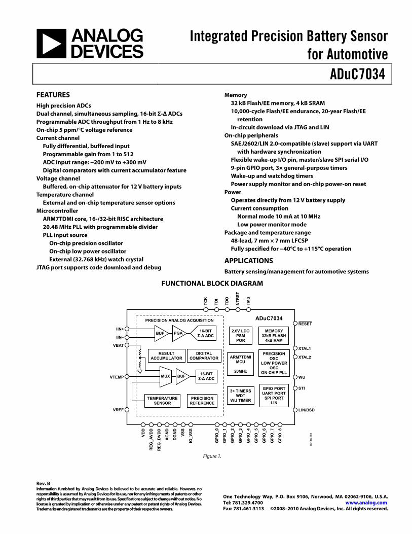
FEATURES High precision ADCs Dual channel, simultaneous sampling, 16-bit Σ-Δ ADCs Programmable ADC throughput from 1 Hz to 8 kHz On-chip 5 ppm/°C voltage reference Current channel
Fully differential, buffered input Programmable gain from 1 to 512 ADC input range: −200 mV to +300 mV Digital comparators with current accumulator feature
Voltage channel Buffered, on-chip attenuator for 12 V battery inputs
Temperature channel External and on-chip temperature sensor options
Changes to Table 6 .......................................................................... 15 Changes to Timers Section ............................................................ 71
8/09—Rev. 0 to Rev. A
Changes to Features Section ............................................................ 1 Changes to Table 1 ............................................................................ 4 Added Exposed Pad Notation to Figure 7 and Table 7 .............. 16 Changes to Theory of Operation .................................................. 20 Changes to Table 45 ........................................................................ 65 Changes to Figure 35 ...................................................................... 78 Changes to Table 96 ......................................................................128 Changes to Figure 57 ....................................................................131 4/08—Revision 0: Initial Version
ADuC7034
Rev. B | Page 4 of 136
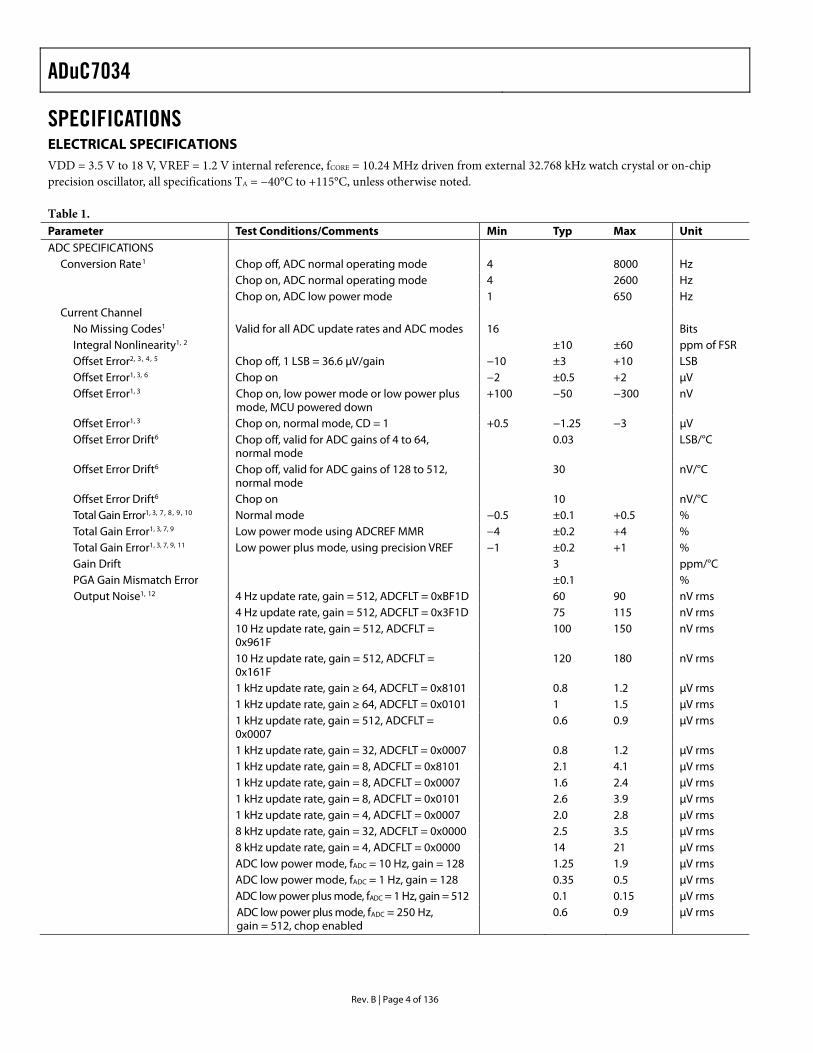
SPECIFICATIONS ELECTRICAL SPECIFICATIONS VDD = 3.5 V to 18 V, VREF = 1.2 V internal reference, fCORE = 10.24 MHz driven from external 32.768 kHz watch crystal or on-chip precision oscillator, all specifications TA = −40°C to +115°C, unless otherwise noted.
Table 1. Parameter Test Conditions/Comments Min Typ Max Unit ADC SPECIFICATIONS
Conversion Rate1 Chop off, ADC normal operating mode 4 8000 Hz Chop on, ADC normal operating mode 4 2600 Hz Chop on, ADC low power mode 1 650 Hz
Current Channel No Missing Codes1 Valid for all ADC update rates and ADC modes 16 Bits Integral Nonlinearity1, 2 ±10 ±60 ppm of FSR Offset Error2, 3 , 4 , 5 Chop off, 1 LSB = 36.6 μV/gain −10 ±3 +10 LSB Offset Error1, 3, 6 Chop on −2 ±0.5 +2 μV Offset Error1, 3 Chop on, low power mode or low power plus
mode, MCU powered down +100 −50 −300 nV
Offset Error1, 3 Chop on, normal mode, CD = 1 +0.5 −1.25 −3 μV Offset Error Drift6 Chop off, valid for ADC gains of 4 to 64,
normal mode 0.03 LSB/°C
Offset Error Drift6 Chop off, valid for ADC gains of 128 to 512, normal mode
30 nV/°C
Offset Error Drift6 Chop on 10 nV/°C Total Gain Error1, 3, 7 , 8 , 9 , 10 Normal mode −0.5 ±0.1 +0.5 % Total Gain Error1, 3, 7, 9 Low power mode using ADCREF MMR −4 ±0.2 +4 % Total Gain Error1, 3, 7, 9, 11 Low power plus mode, using precision VREF −1 ±0.2 +1 % Gain Drift 3 ppm/°C PGA Gain Mismatch Error ±0.1 % Output Noise1, 12 4 Hz update rate, gain = 512, ADCFLT = 0xBF1D 60 90 nV rms 4 Hz update rate, gain = 512, ADCFLT = 0x3F1D 75 115 nV rms
1 kHz update rate, gain = 4, ADCFLT = 0x0007 2.0 2.8 μV rms 8 kHz update rate, gain = 32, ADCFLT = 0x0000 2.5 3.5 μV rms 8 kHz update rate, gain = 4, ADCFLT = 0x0000 14 21 μV rms ADC low power mode, fADC = 10 Hz, gain = 128 1.25 1.9 μV rms ADC low power mode, fADC = 1 Hz, gain = 128 0.35 0.5 μV rms ADC low power plus mode, fADC = 1 Hz, gain = 512 0.1 0.15 μV rms ADC low power plus mode, fADC = 250 Hz,
gain = 512, chop enabled 0.6 0.9 μV rms
ADuC7034
Rev. B | Page 5 of 136
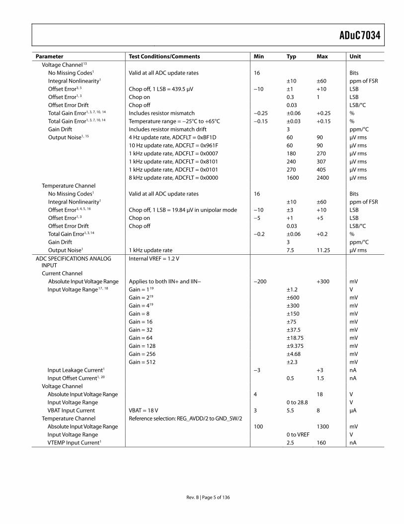
Parameter Test Conditions/Comments Min Typ Max Unit Voltage Channel13
No Missing Codes1 Valid at all ADC update rates 16 Bits Integral Nonlinearity1 ±10 ±60 ppm of FSR Offset Error3, 5 Chop off, 1 LSB = 439.5 μV −10 ±1 +10 LSB Offset Error1, 3 Chop on 0.3 1 LSB Offset Error Drift Chop off 0.03 LSB/°C Total Gain Error1, 3, 7, 10, 14 Includes resistor mismatch −0.25 ±0.06 +0.25 % Total Gain Error1, 3, 7, 10, 14 Temperature range = −25°C to +65°C −0.15 ±0.03 +0.15 % Gain Drift Includes resistor mismatch drift 3 ppm/°C Output Noise1, 15 4 Hz update rate, ADCFLT = 0xBF1D 60 90 μV rms
Temperature Channel No Missing Codes1 Valid at all ADC update rates 16 Bits Integral Nonlinearity1 ±10 ±60 ppm of FSR Offset Error3, 4, 5, 16 Chop off, 1 LSB = 19.84 μV in unipolar mode −10 ±3 +10 LSB Offset Error1, 3 Chop on −5 +1 +5 LSB Offset Error Drift Chop off 0.03 LSB/°C Total Gain Error1, 3, 14 −0.2 ±0.06 +0.2 % Gain Drift 3 ppm/°C Output Noise1 1 kHz update rate 7.5 11.25 μV rms
ADC SPECIFICATIONS ANALOG INPUT
Internal VREF = 1.2 V
Current Channel Absolute Input Voltage Range Applies to both IIN+ and IIN− −200 +300 mV Input Voltage Range17, 18 Gain = 119 ±1.2 V
Gain = 219 ±600 mV Gain = 419 ±300 mV Gain = 8 ±150 mV Gain = 16 ±75 mV Gain = 32 ±37.5 mV Gain = 64 ±18.75 mV Gain = 128 ±9.375 mV Gain = 256 ±4.68 mV Gain = 512 ±2.3 mV
Input Leakage Current1 −3 +3 nA Input Offset Current1, 20 0.5 1.5 nA
Voltage Channel Absolute Input Voltage Range 4 18 V Input Voltage Range 0 to 28.8 V VBAT Input Current VBAT = 18 V 3 5.5 8 μA
Temperature Channel Reference selection: REG_AVDD/2 to GND_SW/2 Absolute Input Voltage Range 100 1300 mV Input Voltage Range 0 to VREF V VTEMP Input Current1 2.5 160 nA
ADuC7034
Rev. B | Page 6 of 136
Parameter Test Conditions/Comments Min Typ Max Unit VOLTAGE REFERENCE
ADC Precision Reference Internal VREF 1.2 V Power-Up Time1 0.5 ms Initial Accuracy1 Measured at TA = 25°C −0.15 +0.15 % Temperature Coefficient1, 21 −20 ±5 +20 ppm/°C Reference Long-Term Stability22 100 ppm/1000 hr
External Reference Input Range23 0.1 1.3 V VREF Divide-by-2 Initial Error1 0.1 0.3 % ADC Low Power Reference
Internal VREF 1.2 V Initial Accuracy Measured at TA = 25°C −5 +5 % Initial Accuracy1 Using ADCREF, measured at TA = 25°C 0.1 % Temperature Coefficient1, 21 −300 ±150 +300 ppm/°C
ADC DIAGNOSTICS VREF/1361 At any gain settings 8.5 9.4 mV Voltage Attenuator Current
Source1 Differential voltage increase on the attenuator when the current source is on, over a range of TA = −40°C to +85°C
3.1 3.8 V
RESISTIVE ATTENUATOR Divider Ratio 24 Resistor Mismatch Drift 3 ppm/°C
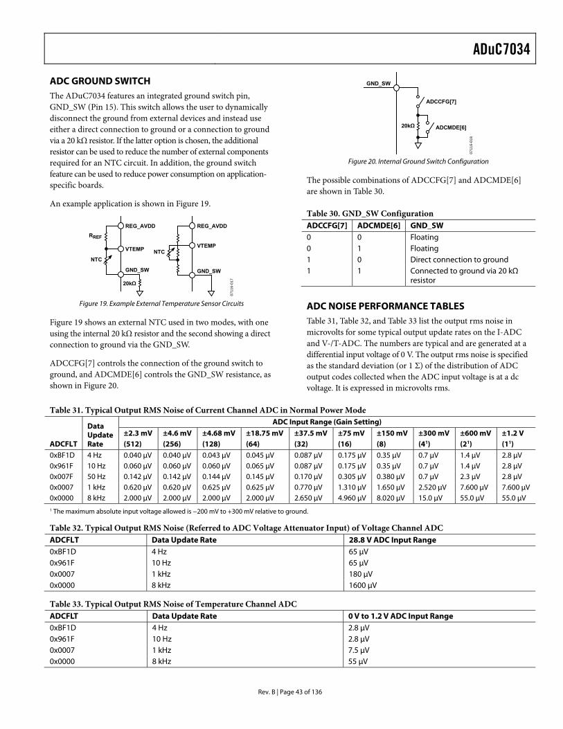
ADC GROUND SWITCH Resistance Direct path to ground 10 Ω
20 kΩ resistor selected1 10 20 30 kΩ Input Current Allowed continuous current through the switch
with direct path to ground 6 mA
TEMPERATURE SENSOR24 After user calibration Accuracy MCU in power-down or standby mode ±3 °C
MCU in power-down or standby mode, temperature range = −25°C to +65°C
±2 °C
POWER-ON RESET (POR) POR Trip Level Refers to the voltage at the VDD pin 2.85 3.0 3.15 V POR Hysteresis 300 mV Reset Timeout from POR 20 ms
LOW VOLTAGE FLAG (LVF) LVF Level Refers to the voltage at the VDD pin 1.9 2.1 2.3 V
POWER SUPPLY MONITOR (PSM) PSM Trip Level Refers to the voltage at the VDD pin 6.0 V
FLASH/EE MEMORY1 Endurance25 10,000 Cycles Data Retention26 20 Years
DIGITAL INPUTS All digital inputs except NTRST Input Leakage Current Input high = REG_DVDD ±1 ±10 μA Input Pull-Up Current Input low = 0 V −80 −20 −10 μA Input Capacitance 10 pF Input Leakage Current NTRST only: input low = 0 V ±1 ±10 μA Input Pull-Down Current NTRST only: input high = REG_DVDD 30 55 100 μA
ADuC7034
Rev. B | Page 7 of 136
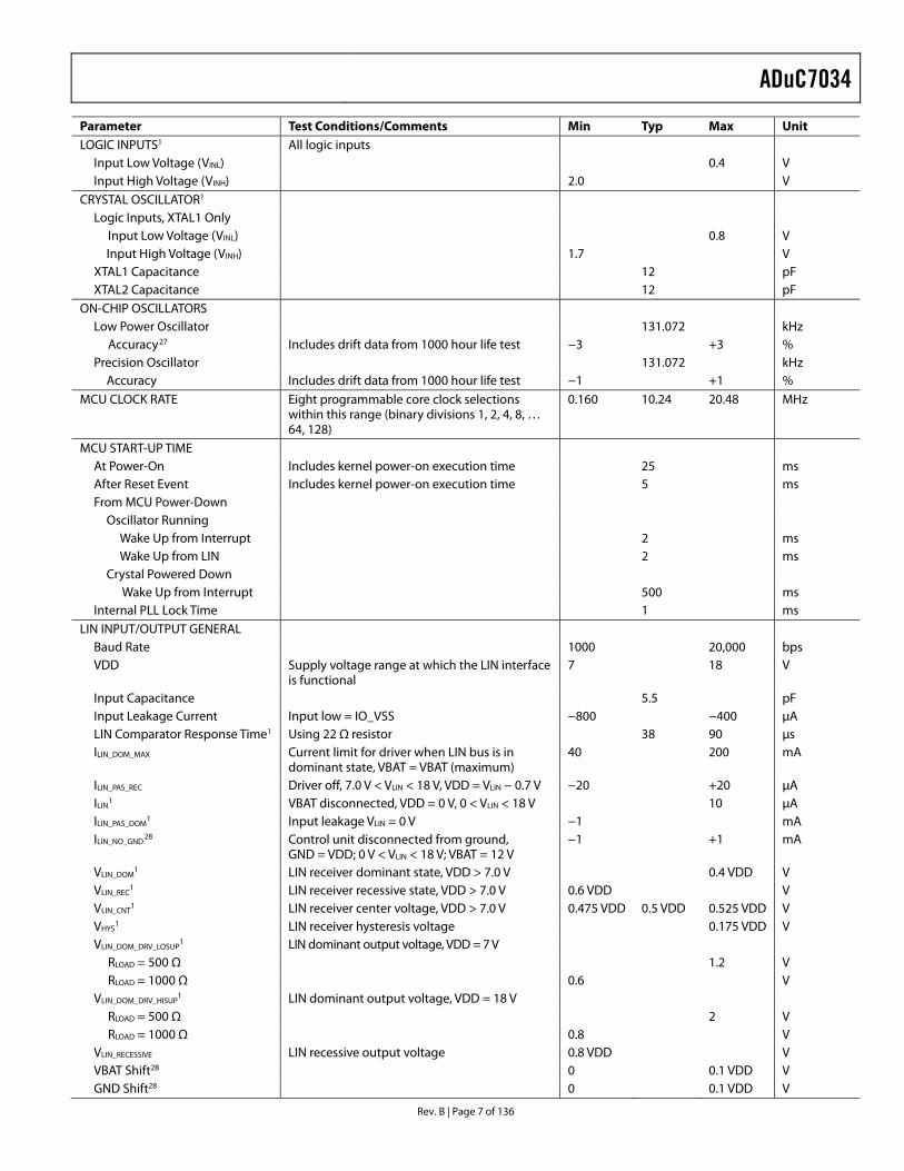
Parameter Test Conditions/Comments Min Typ Max Unit LOGIC INPUTS1 All logic inputs
Input Low Voltage (VINL) 0.4 V Input High Voltage (VINH) 2.0 V
CRYSTAL OSCILLATOR1 Logic Inputs, XTAL1 Only
Input Low Voltage (VINL) 0.8 V Input High Voltage (VINH) 1.7 V
XTAL1 Capacitance 12 pF XTAL2 Capacitance 12 pF
ON-CHIP OSCILLATORS Low Power Oscillator 131.072 kHz
Accuracy27 Includes drift data from 1000 hour life test −3 +3 % Precision Oscillator 131.072 kHz
Accuracy Includes drift data from 1000 hour life test −1 +1 % MCU CLOCK RATE Eight programmable core clock selections
within this range (binary divisions 1, 2, 4, 8, … 64, 128)
0.160 10.24 20.48 MHz
MCU START-UP TIME At Power-On Includes kernel power-on execution time 25 ms After Reset Event Includes kernel power-on execution time 5 ms From MCU Power-Down
Oscillator Running Wake Up from Interrupt 2 ms Wake Up from LIN 2 ms
Crystal Powered Down Wake Up from Interrupt 500 ms
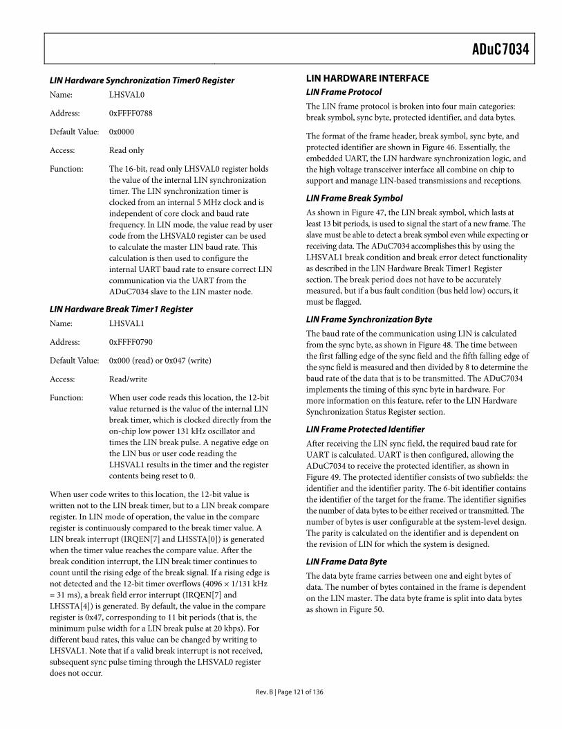
Internal PLL Lock Time 1 ms LIN INPUT/OUTPUT GENERAL
Baud Rate 1000 20,000 bps VDD Supply voltage range at which the LIN interface
is functional 7 18 V
Input Capacitance 5.5 pF Input Leakage Current Input low = IO_VSS −800 −400 μA LIN Comparator Response Time1 Using 22 Ω resistor 38 90 μs ILIN_DOM_MAX Current limit for driver when LIN bus is in
dominant state, VBAT = VBAT (maximum) 40 200 mA
ILIN_PAS_REC Driver off, 7.0 V < VLIN < 18 V, VDD = VLIN − 0.7 V −20 +20 μA ILIN
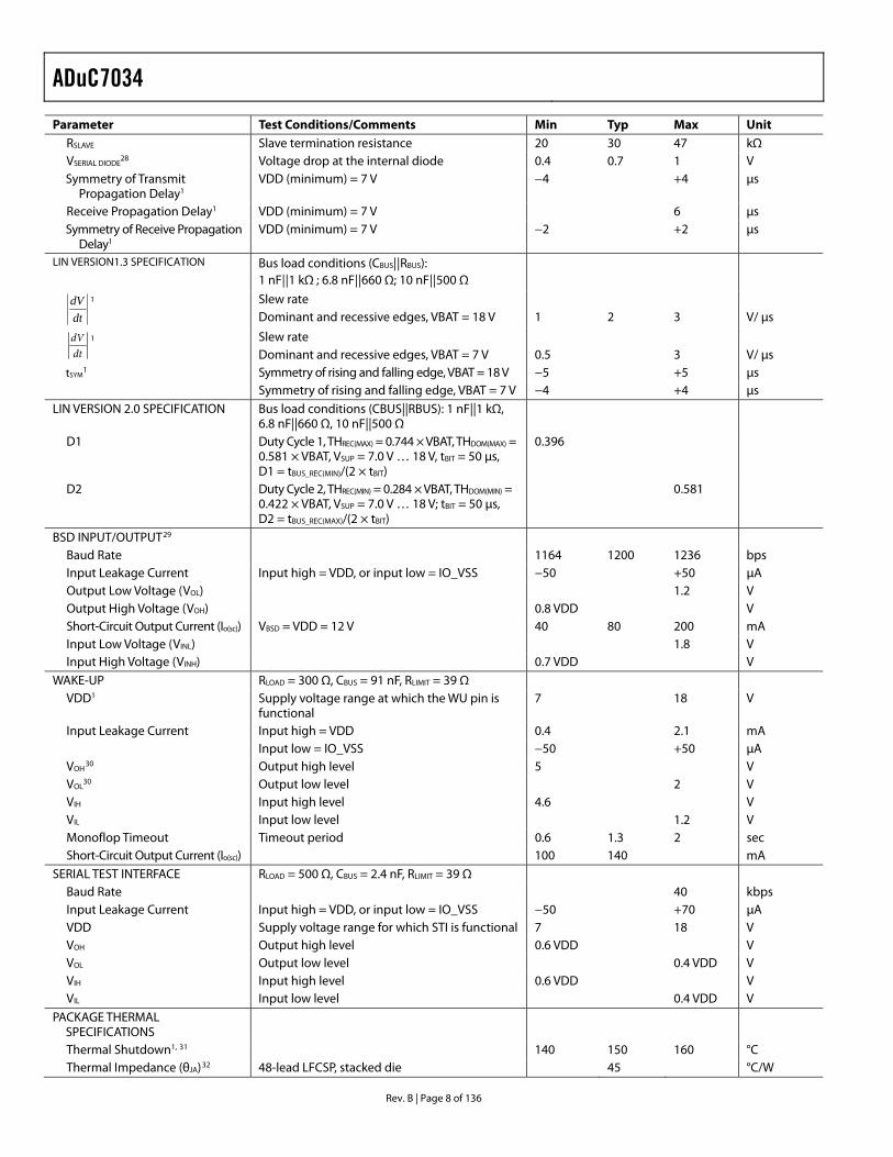
BSD INPUT/OUTPUT29 Baud Rate 1164 1200 1236 bps Input Leakage Current Input high = VDD, or input low = IO_VSS −50 +50 μA Output Low Voltage (VOL) 1.2 V Output High Voltage (VOH) 0.8 VDD V Short-Circuit Output Current (Io(sc)) VBSD = VDD = 12 V 40 80 200 mA Input Low Voltage (VINL) 1.8 V Input High Voltage (VINH) 0.7 VDD V
WAKE-UP RLOAD = 300 Ω, CBUS = 91 nF, RLIMIT = 39 Ω VDD1 Supply voltage range at which the WU pin is
functional 7 18 V
Input Leakage Current Input high = VDD 0.4 2.1 mA Input low = IO_VSS −50 +50 μA VOH
30 Output high level 5 V VOL
30 Output low level 2 V VIH Input high level 4.6 V VIL Input low level 1.2 V Monoflop Timeout Timeout period 0.6 1.3 2 sec Short-Circuit Output Current (Io(sc)) 100 140 mA
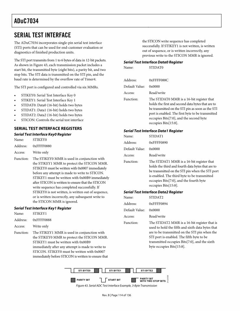
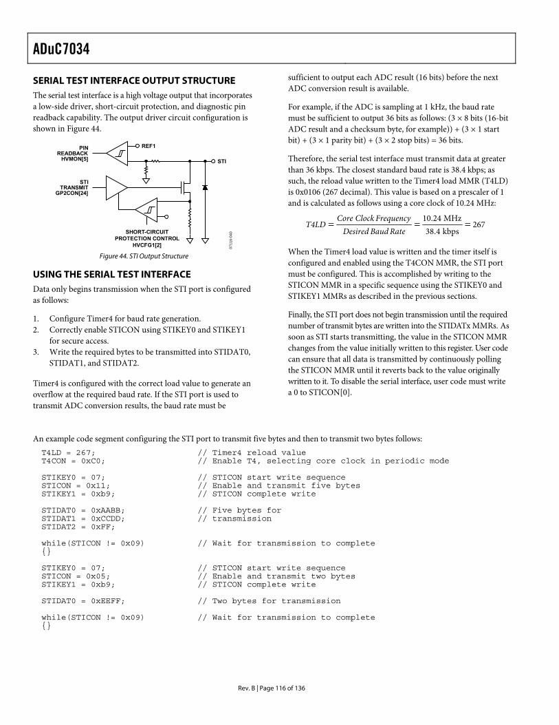
SERIAL TEST INTERFACE RLOAD = 500 Ω, CBUS = 2.4 nF, RLIMIT = 39 Ω Baud Rate 40 kbps Input Leakage Current Input high = VDD, or input low = IO_VSS −50 +70 μA VDD Supply voltage range for which STI is functional 7 18 V VOH Output high level 0.6 VDD V VOL Output low level 0.4 VDD V VIH Input high level 0.6 VDD V VIL Input low level 0.4 VDD V
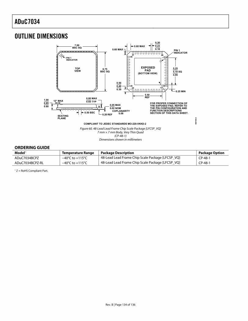
PACKAGE THERMAL SPECIFICATIONS
Thermal Shutdown1, 31 140 150 160 °C Thermal Impedance (θJA)32 48-lead LFCSP, stacked die 45 °C/W
ADuC7034
Rev. B | Page 9 of 136
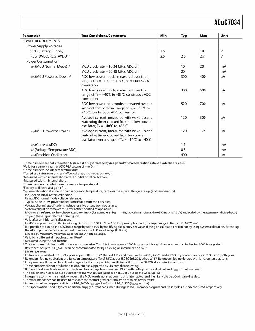
Parameter Test Conditions/Comments Min Typ Max Unit POWER REQUIREMENTS
Power Supply Voltages VDD (Battery Supply) 3.5 18 V REG_DVDD, REG_AVDD33 2.5 2.6 2.7 V
Power Consumption IDD (MCU Normal Mode)34 MCU clock rate = 10.24 MHz, ADC off 10 20 mA MCU clock rate = 20.48 MHz, ADC off 20 mA IDD (MCU Powered Down)1 ADC low power mode, measured over the
range of TA = −10°C to +40°C, continuous ADC conversion
300 400 μA
ADC low power mode, measured over the range of TA = −40°C to +85°C, continuous ADC conversion
300 500 μA
ADC low power plus mode, measured over an ambient temperature range of TA = −10°C to +40°C, continuous ADC conversion
520 700 μA
Average current, measured with wake-up and watchdog timer clocked from the low power oscillator, TA = −40°C to +85°C
120 300 μA
IDD (MCU Powered Down) Average current, measured with wake-up and watchdog timer clocked from low power oscillator over a range of TA = −10°C to +40°C
120 175 μA
IDD (Current ADC) 1.7 mA IDD (Voltage/Temperature ADC) 0.5 mA IDD (Precision Oscillator) 400 μA
1 These numbers are not production tested, but are guaranteed by design and/or characterization data at production release. 2 Valid for a current channel ADC PGA setting of 4 to 64. 3 These numbers include temperature drift. 4 Tested at a gain range of 4; self-offset calibration removes this error. 5 Measured with an internal short after an initial offset calibration. 6 Measured with an internal short. 7 These numbers include internal reference temperature drift. 8 Factory calibrated at a gain of 1. 9 System calibration at a specific gain range (and temperature) removes the error at this gain range (and temperature). 10 Includes an initial system calibration. 11 Using ADC normal mode voltage reference. 12 Typical noise in low power modes is measured with chop enabled. 13 Voltage channel specifications include resistive attenuator input stage. 14 System calibration removes this error at the specified temperature. 15 RMS noise is referred to the voltage attenuator input (for example, at fADC = 1 kHz, typical rms noise at the ADC input is 7.5 μV) and scaled by the attenuator (divide-by-24)
to yield these input-referred noise figures. 16 Valid after an initial self-calibration. 17 In ADC low power mode, the input range is fixed at ±9.375 mV. In ADC low power plus mode, the input range is fixed at ±2.34375 mV. 18 It is possible to extend the ADC input range by up to 10% by modifying the factory-set value of the gain calibration register or by using system calibration. Extending
the ADC input range can also be used to reduce the ADC input range (LSB size). 19 Limited by minimum/maximum absolute input voltage range. 20 Valid for a differential input less than 10 mV. 21 Measured using the box method. 22 The long-term stability specification is noncumulative. The drift in subsequent 1000 hour periods is significantly lower than in the first 1000 hour period. 23 References of up to REG_AVDD can be accommodated for by enabling an internal divide-by-2. 24 Die temperature. 25 Endurance is qualified to 10,000 cycles as per JEDEC Std. 22 Method A117 and measured at −40°C, +25°C, and +125°C. Typical endurance at 25°C is 170,000 cycles. 26 Retention lifetime equivalent at a junction temperature (TJ) of 85°C as per JEDEC Std. 22 Method A117. Retention lifetime derates with junction temperature. 27 Low power oscillator can be calibrated against either the precision oscillator or the external 32.768 kHz crystal in user code. 28 These numbers are not production tested, but are supported by LIN compliance testing. 29 BSD electrical specifications, except high and low voltage levels, are per LIN 2.0 with pull-up resistor disabled and CLoad = 10 nF maximum. 30 This specification does not apply directly to the WU pin but includes an RLIMIT of 39 Ω on the wake-up line. 31 In response to a thermal shutdown event, the MCU core is not shut down but is interrupted, and the high voltage I/O pins are disabled. 32 Thermal impedance can be used to calculate the thermal gradient from ambient to die temperature. 33 Internal regulated supply available at REG_DVDD (ISOURCE = 5 mA) and REG_AVDD (ISOURCE = 1 mA). 34 The specification listed is typical; additional supply current consumed during Flash/EE memory program and erase cycles is 7 mA and 5 mA, respectively.
ADuC7034
Rev. B | Page 10 of 136
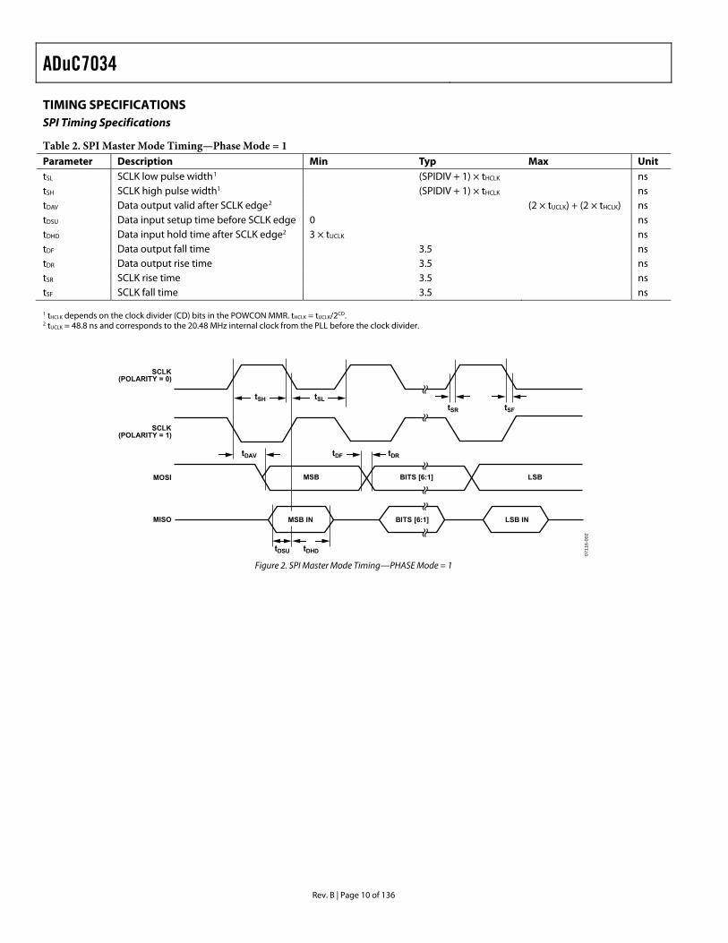
TIMING SPECIFICATIONS SPI Timing Specifications
Table 2. SPI Master Mode Timing—Phase Mode = 1 Parameter Description Min Typ Max Unit tSL SCLK low pulse width1 (SPIDIV + 1) × tHCLK ns tSH SCLK high pulse width1 (SPIDIV + 1) × tHCLK ns tDAV Data output valid after SCLK edge2 (2 × tUCLK) + (2 × tHCLK) ns tDSU Data input setup time before SCLK edge 0 ns tDHD Data input hold time after SCLK edge2 3 × tUCLK ns tDF Data output fall time 3.5 ns tDR Data output rise time 3.5 ns tSR SCLK rise time 3.5 ns tSF SCLK fall time 3.5 ns 1 tHCLK depends on the clock divider (CD) bits in the POWCON MMR. tHCLK = tUCLK/2CD. 2 tUCLK = 48.8 ns and corresponds to the 20.48 MHz internal clock from the PLL before the clock divider.
SCLK(POLARITY = 0)
SCLK(POLARITY = 1)
MOSI
MISO MSB IN BITS [6:1] LSB IN
LSBBITS [6:1]MSB
tSH tSLtSR
tDAV tDF tDR
tDSU tDHD
tSF
0711
6-00
2
Figure 2. SPI Master Mode Timing—PHASE Mode = 1
ADuC7034
Rev. B | Page 11 of 136
Table 3. SPI Master Mode Timing—PHASE Mode = 0 Parameter Description Min Typ Max Unit tSL SCLK low pulse width1 (SPIDIV + 1) × tHCLK ns tSH SCLK high pulse width1 (SPIDIV + 1) × tHCLK ns tDAV Data output valid after SCLK edge2 (2 × tUCLK) + (2 × tHCLK) ns tDOSU Data output setup before SCLK edge ½ tSL ns tDSU Data input setup time before SCLK edge 0 ns tDHD Data input hold time after SCLK edge2 3 × tUCLK ns tDF Data output fall time 3.5 ns tDR Data output rise time 3.5 ns tSR SCLK rise time 3.5 ns tSF SCLK fall time 3.5 ns 1 tHCLK depends on the clock divider (CD) bits in the POWCON MMR. tHCLK = tUCLK/2CD. 2 tUCLK = 48.8 ns and corresponds to the 20.48 MHz internal clock from the PLL before the clock divider.
SCLK(POLARITY = 0)
SCLK(POLARITY = 1)
tSH tSLtSR tSF
MISO MSB IN BITS [6:1] LSB IN
tDSU tDHD
MOSI LSBBITS [6:1]MSB
tDAV
tDF tDRtDOSU
0711
6-00
3
Figure 3. SPI Master Mode Timing—PHASE Mode = 0
ADuC7034
Rev. B | Page 12 of 136
Table 4. SPI Slave Mode Timing—PHASE Mode = 1 Parameter Description Min Typ Max Unit
tSS SS to SCLK edge ½ tSL ns
tSL SCLK low pulse width1 (SPIDIV + 1) × tHCLK ns tSH SCLK high pulse width1 (SPIDIV + 1) × tHCLK ns tDAV Data output valid after SCLK edge2 (3 × tUCLK) + (2 × tHCLK) ns tDSU Data input setup time before SCLK edge 0 ns tDHD Data input hold time after SCLK edge2 4 × tUCLK ns tDF Data output fall time 3.5 ns tDR Data output rise time 3.5 ns tSR SCLK rise time 3.5 ns tSF SCLK fall time 3.5 ns tSFS SS high after SCLK edge ½ tSL ns 1 tHCLK depends on the clock divider (CD) bits in the POWCON MMR. tHCLK = tUCLK/2CD. 2 tUCLK = 48.8 ns and corresponds to the 20.48 MHz internal clock from the PLL before the clock divider.
MOSI MSB IN BITS [6:1] LSB IN
tDSU tDHD
SCLK(POLARITY = 0)
SS
SCLK(POLARITY = 1)
tSH
tCS
tSLtSR tSF
tDAV
MISO LSBBITS [6:1]MSB
tDF tDR
tSFS
0711
6-00
4
Figure 4. SPI Slave Mode Timing—PHASE Mode = 1
ADuC7034
Rev. B | Page 13 of 136
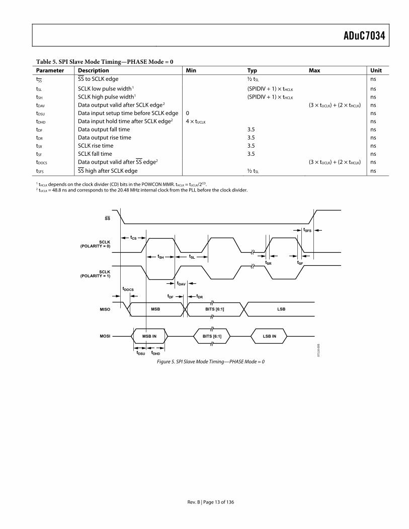
Table 5. SPI Slave Mode Timing—PHASE Mode = 0 Parameter Description Min Typ Max Unit tSS SS to SCLK edge ½ tSL ns
tSL SCLK low pulse width1 (SPIDIV + 1) × tHCLK ns tSH SCLK high pulse width1 (SPIDIV + 1) × tHCLK ns tDAV Data output valid after SCLK edge2 (3 × tUCLK) + (2 × tHCLK) ns tDSU Data input setup time before SCLK edge 0 ns tDHD Data input hold time after SCLK edge2 4 × tUCLK ns tDF Data output fall time 3.5 ns tDR Data output rise time 3.5 ns tSR SCLK rise time 3.5 ns tSF SCLK fall time 3.5 ns tDOCS Data output valid after SS edge2 (3 × tUCLK) + (2 × tHCLK) ns
tSFS SS high after SCLK edge ½ tSL ns 1 tHCLK depends on the clock divider (CD) bits in the POWCON MMR. tHCLK = tUCLK/2CD. 2 tUCLK = 48.8 ns and corresponds to the 20.48 MHz internal clock from the PLL before the clock divider.
SCLK(POLARITY = 0)
SS
SCLK(POLARITY = 1)
tSH
tCS
tSLtSR tSF
tSFS
MOSI MSB IN BITS [6:1] LSB IN
tDSU tDHD
tDAV
MISO LSBBITS [6:1]MSB
tDF tDR
tDOCS
0711
6-00
5
Figure 5. SPI Slave Mode Timing—PHASE Mode = 0
ADuC7034
Rev. B | Page 14 of 136
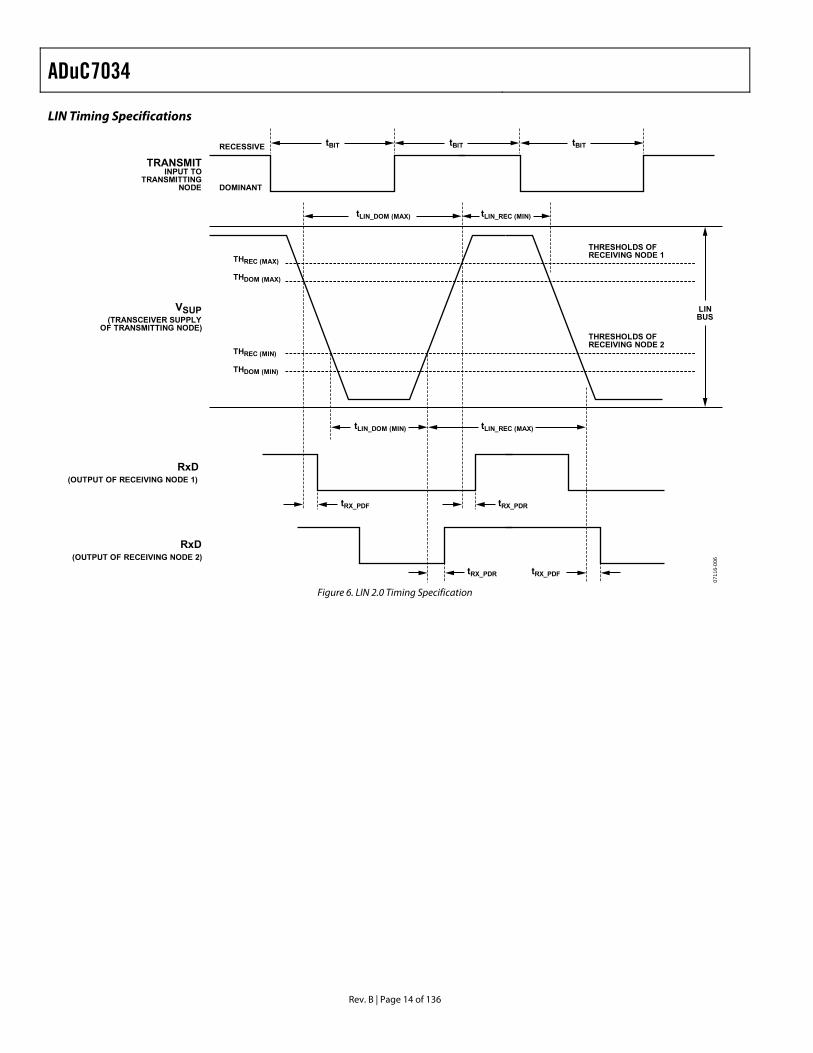
LIN Timing Specifications
TRANSMITINPUT TO
TRANSMITTINGNODE
VSUP(TRANSCEIVER SUPPLY
OF TRANSMITTING NODE)
RxD(OUTPUT OF RECEIVING NODE 1)
RxD(OUTPUT OF RECEIVING NODE 2)
RECESSIVE
THREC (MAX)
tLIN_DOM (MAX) tLIN_REC (MIN)
tLIN_DOM (MIN) tLIN_REC (MAX)
THDOM (MAX)
THREC (MIN)
THDOM (MIN)
DOMINANT
THRESHOLDS OFRECEIVING NODE 1
LINBUS
THRESHOLDS OFRECEIVING NODE 2
tBIT tBIT tBIT
tRX_PDR
tRX_PDR
tRX_PDF
tRX_PDF
0711
6-00
6
Figure 6. LIN 2.0 Timing Specification
ADuC7034
Rev. B | Page 15 of 136
ABSOLUTE MAXIMUM RATINGS TA = −40°C to +115°C, unless otherwise noted.
Table 6.
Stresses above those listed under Absolute Maximum Ratings may cause permanent damage to the device. This is a stress rating only; functional operation of the device at these or any other conditions above those indicated in the operational section of this specification is not implied. Exposure to absolute maximum rating conditions for extended periods may affect device reliability.
Parameter Rating AGND to DGND to VSS to IO_VSS −0.3 V to +0.3 V VBAT to AGND −22 V to +40 V VDD to VSS −0.3 V to +33 V VDD to VSS for 1 sec −0.3 V to +40 V LIN to IO_VSS −16 V to +40 V STI and WU to IO_VSS −3 V to +33 V Wake-Up Continuous Current 50 mA Short-Circuit Current of High
Voltage I/O Pins 100 mA
Digital I/O Voltage to DGND −0.3 V to REG_DVDD + 0.3 V VREF to AGND −0.3 V to REG_AVDD + 0.3 V ADC Inputs to AGND −0.3 V to REG_AVDD + 0.3 V ESD Human Body Model (HBM) Rating
HBM-ADI0082 (Based on ANSI/ESD STM5.1-2007).
All Pins except LIN and VBAT
1 kV
LIN and VBAT ±6KV IEC 61000-4-2 for LIN and VBAT ±7 kV
Storage Temperature 125°C Junction Temperature
Transient 150°C Continuous 130°C
Lead Temperature Soldering Reflow (15 sec) 260°C
ESD CAUTION
ADuC7034
Rev. B | Page 16 of 136
13 14 15 16 17 18 19 20 21 22 23 24
VBAT
VREF
GN
D_S
W NC
NC
VTEM
PIIN
+IIN
–A
GN
DA
GN
DN
CR
EG_A
VDD
48 47 46 45 44 43 42 41 40 39 38 37
LIN
/BS
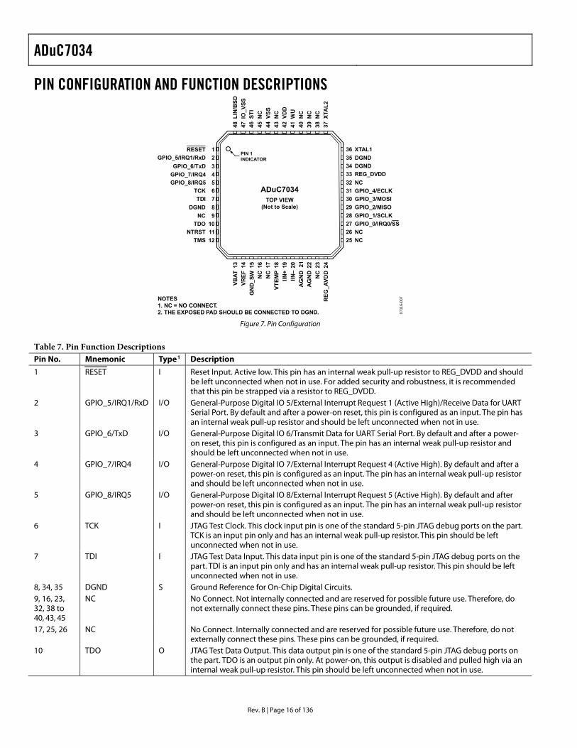
PIN CONFIGURATION AND FUNCTION DESCRIPTIONS
DIO
_VSS
STI
NC
VSS
NC
VDD
WU
NC
NC
NC
XTA
L2
123456789
101112
RESETGPIO_5/IRQ1/RxD
GPIO_6/TxDGPIO_7/IRQ4GPIO_8/IRQ5
TCKTDI
DGNDNC
TDONTRST
TMS
NOTES1. NC = NO CONNECT.2. THE EXPOSED PAD SHOULD BE CONNECTED TO DGND.
Table 7. Pin Function Descriptions Pin No. Mnemonic Type1 Description
1 RESET I Reset Input. Active low. This pin has an internal weak pull-up resistor to REG_DVDD and should be left unconnected when not in use. For added security and robustness, it is recommended that this pin be strapped via a resistor to REG_DVDD.
2 GPIO_5/IRQ1/RxD I/O General-Purpose Digital IO 5/External Interrupt Request 1 (Active High)/Receive Data for UART Serial Port. By default and after a power-on reset, this pin is configured as an input. The pin has an internal weak pull-up resistor and should be left unconnected when not in use.
3 GPIO_6/TxD I/O General-Purpose Digital IO 6/Transmit Data for UART Serial Port. By default and after a power-on reset, this pin is configured as an input. The pin has an internal weak pull-up resistor and should be left unconnected when not in use.
4 GPIO_7/IRQ4 I/O General-Purpose Digital IO 7/External Interrupt Request 4 (Active High). By default and after a power-on reset, this pin is configured as an input. The pin has an internal weak pull-up resistor and should be left unconnected when not in use.
5 GPIO_8/IRQ5 I/O General-Purpose Digital IO 8/External Interrupt Request 5 (Active High). By default and after power-on reset, this pin is configured as an input. The pin has an internal weak pull-up resistor and should be left unconnected when not in use.
6 TCK I JTAG Test Clock. This clock input pin is one of the standard 5-pin JTAG debug ports on the part. TCK is an input pin only and has an internal weak pull-up resistor. This pin should be left unconnected when not in use.
7 TDI I JTAG Test Data Input. This data input pin is one of the standard 5-pin JTAG debug ports on the part. TDI is an input pin only and has an internal weak pull-up resistor. This pin should be left unconnected when not in use.
8, 34, 35 DGND S Ground Reference for On-Chip Digital Circuits. 9, 16, 23, 32, 38 to 40, 43, 45
NC No Connect. Not internally connected and are reserved for possible future use. Therefore, do not externally connect these pins. These pins can be grounded, if required.
17, 25, 26 NC No Connect. Internally connected and are reserved for possible future use. Therefore, do not externally connect these pins. These pins can be grounded, if required.
10 TDO O JTAG Test Data Output. This data output pin is one of the standard 5-pin JTAG debug ports on the part. TDO is an output pin only. At power-on, this output is disabled and pulled high via an internal weak pull-up resistor. This pin should be left unconnected when not in use.
ADuC7034
Rev. B | Page 17 of 136
Pin No. Mnemonic Type1 Description 11 NTRST I JTAG Test Reset. This reset input pin is one of the standard 5-pin JTAG debug ports on the part.
NTRST is an input pin only and has an internal weak pull-down resistor. This pin should be left unconnected when not in use. NTRST is also monitored by the on-chip kernel to enable LIN boot load mode.
12 TMS I JTAG Test Mode Select. This mode select input pin is one of the standard 5-pin JTAG debug ports on the part. TMS is an input pin only and has an internal weak pull-up resistor. This pin should be left unconnected when not in use.
13 VBAT I Battery Voltage Input to Resistor Divider. 14 VREF I External Reference Input Terminal. When this input is not used, connect it directly to the AGND
system ground. This pin should be left unconnected when not in use. 15 GND_SW I Switch to Internal Analog Ground Reference. This pin is the negative input for the external
temperature channel and the external reference. When this input is not used, connect it directly to the AGND system ground.
18 VTEMP I External Pin for NTC/PTC Temperature Measurement. 19 IIN+ I Positive Differential Input for Current Channel. 20 IIN− I Negative Differential Input for Current Channel. 21, 22 AGND S Ground Reference for On-Chip Precision Analog Circuits. 24 REG_AVDD S Nominal 2.6 V Output from On-Chip Regulator. 27 GPIO_0/IRQ0/SS I/O General-Purpose Digital IO 0/External Interrupt Request 0 (Active High)/Slave Select Input (SPI
Interface). By default and after a power-on reset, this pin is configured as an input. The pin has an internal weak pull-up resistor and should be left unconnected when not in use.
28 GPIO_1/SCLK I/O General-Purpose Digital IO 1/Serial Clock Input (SPI Interface). By default and after a power-on reset, this pin is configured as an input. The pin has an internal weak pull-up resistor and should be left unconnected when not in use.
29 GPIO_2/MISO I/O General-Purpose Digital IO 2/Master Input, Slave Output (SPI Interface). By default and after a power-on reset, this pin is configured as an input. The pin has an internal weak pull-up resistor and should be left unconnected when not in use.
30 GPIO_3/MOSI I/O General-Purpose Digital IO 3/Master Output, Slave Input (SPI Interface). By default and after a power-on reset, this pin is configured as an input. The pin has an internal weak pull-up resistor and should be left unconnected when not in use.
31 GPIO_4/ECLK I/O General-Purpose Digital IO 4/2.56 MHz Clock Output. By default and after a power-on reset, this pin is configured as an input. The pin has an internal weak pull-up resistor and should be left unconnected when not in use.
33 REG_DVDD S Nominal 2.6 V Output from the On-Chip Regulator. 36 XTAL1 O Crystal Oscillator Output. If an external crystal is not used, this pin should be left unconnected. 37 XTAL2 I Crystal Oscillator Input. If an external crystal is not used, connect this pin to the DGND system
ground. 41 WU I/O High Voltage Wake-Up. This high voltage I/O pin has an internal 10 kΩ pull-down resistor and a
high-side driver to VDD. If this pin is not being used, it should not be connected externally. 42 VDD S Battery Power Supply to On-Chip Regulator. 44 VSS S Ground Reference. This is the ground reference for the internal voltage regulators. 46 STI I/O High Voltage Serial Test Interface Output. If this pin is not used, externally connect it to the
IO_VSS ground reference. 47 IO_VSS S Ground Reference for High Voltage I/O Pins. 48 LIN/BSD I/O Local Interconnect Network IO/Bit Serial Device IO. This is a high voltage pin. EPAD Exposed Pad The exposed pad should be connected to digital ground. 1 I = input, O = output, S = supply.
ADuC7034
Rev. B | Page 18 of 136
TYPICAL PERFORMANCE CHARACTERISTICS
–40 –10 20 50 80 115 140
0
–1.2
–1.0
–0.8
–0.6
–0.4
–0.2
OFF
SET
(µV)
TEMPERATURE (°C) 0711
6-05
6
VDD = 4V
VDD = 18V
Figure 8. ADC Current Channel Offset vs. Temperature, 10 MHz MCU
0
–2.5
–2.0
–1.5
–1.0
–0.5
20
OFF
SET
(µV)
VDD (V) 0711
6-05
7
4 6 8 10 12 14 16 18
+115°C
+25°C
–40°C
Figure 9. ADC Current Channel Offset vs. VDD (10 MHz, MCU)
0
–2.5
–2.0
–1.5
–1.0
–0.5
4 6 8 10 12 14 16 18 20
OFF
SET
(µV)
VDD (V)
CORE OFF
CD = 0
CD = 1
0711
6-05
8
Figure 10. ADC Current Channel Offset vs. Supply @ 25°C
ADuC7034
Rev. B | Page 19 of 136
TERMINOLOGY Conversion Rate The conversion rate specifies the rate at which an output result is available from the ADC after the ADC has settled.
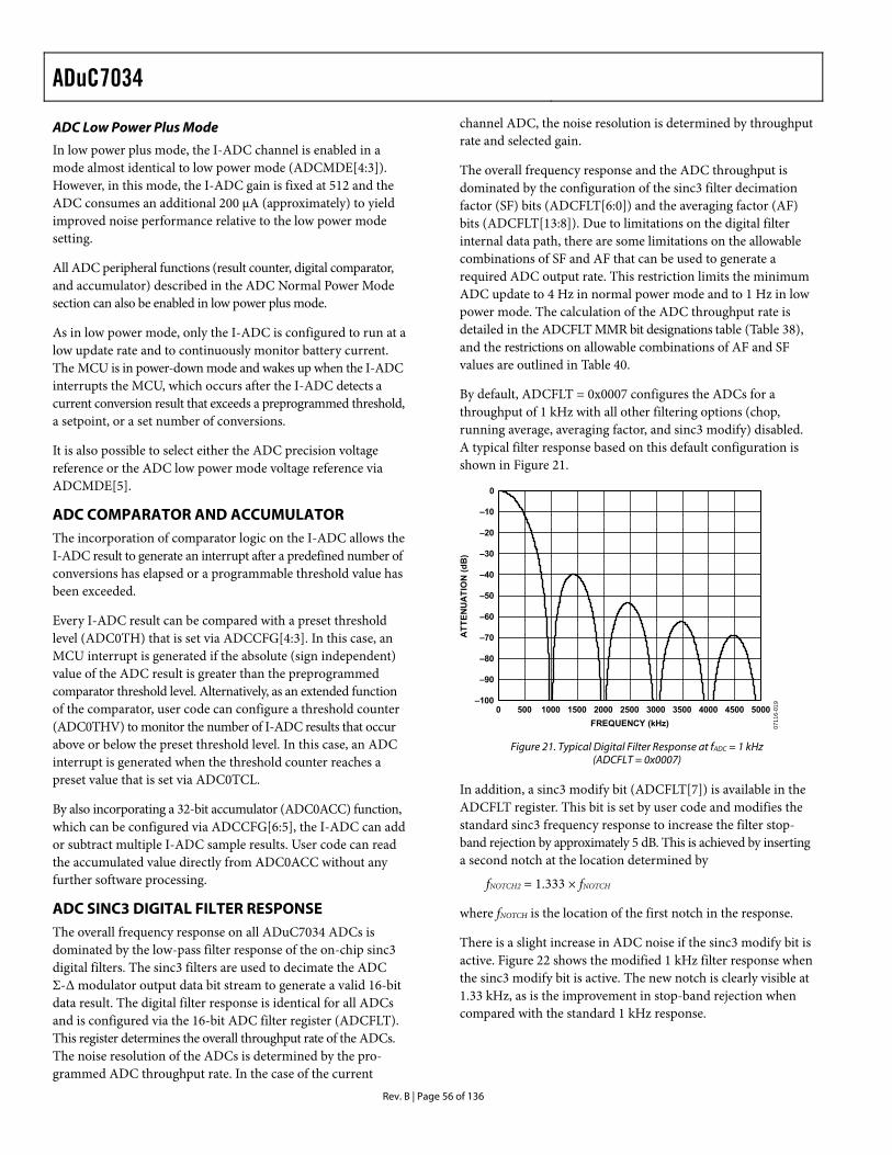
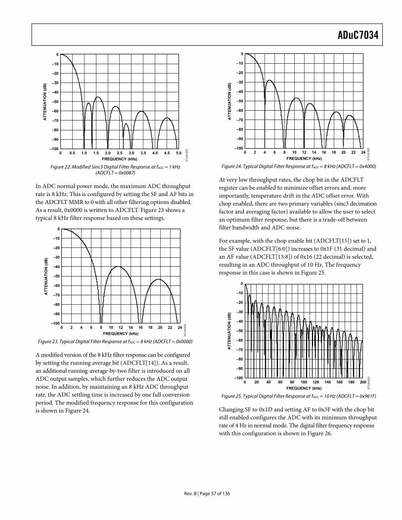
The Σ-Δ conversion techniques used on this part mean that while the ADC front-end signal is oversampled at a relatively high sample rate, a subsequent digital filter is used to decimate the output, providing a valid 16-bit data conversion result for output rates from 1 Hz to 8 kHz.
Note that when software switches from one input to another on the same ADC, the digital filter must first be cleared and then allowed to average a new result. Depending on the configuration of the ADC and the type of filter, this may require multiple conversion cycles.
Integral Nonlinearity (INL) INL is the maximum deviation of any code from a straight line passing through the endpoints of the transfer function. The end-points of the transfer function are zero scale, a point ½ LSB below the first code transition, and full scale, a point ½ LSB above the last code transition (111 ... 110 to 111 ... 111). The error is expressed as a percentage of full scale.
No Missing Codes No missing codes is a measure of the differential nonlinearity of the ADC. The error is expressed in bits (as 2N bits, where N is no missing codes) and specifies the number of codes (ADC results) that are guaranteed to occur through the full ADC input range.
Offset Error Offset error is the deviation of the first code transition ADC input voltage from the ideal first code transition.
Offset Error Drift Offset error drift is the variation in absolute offset error with respect to temperature. This error is expressed as LSBs per degrees Celsius.
Gain Error Gain error is a measure of the span error of the ADC. It is a measure of the difference between the measured and the ideal span between any two points in the transfer function.
Output Noise The output noise is specified as the standard deviation (that is, 1 × Σ) of the distribution of ADC output codes that are collected when the ADC input voltage is at a dc voltage. It is expressed as μV rms. The output, or rms noise, can be used to calculate the effective resolution of the ADC as defined by the following equation:
The peak-to-peak noise is defined as the deviation of codes that fall within 6.6 × Σ of the distribution of ADC output codes that are collected when the ADC input voltage is at dc. The peak-to-peak noise is therefore calculated as 6.6 times the rms noise.
The peak-to-peak noise can be used to calculate the ADC (noise-free code) resolution for which there is no code flicker within a 6.6 × Σ limit as defined by the following equation:
where Noise-Free Code Resolution is expressed in bits.
ADuC7034
Rev. B | Page 20 of 136
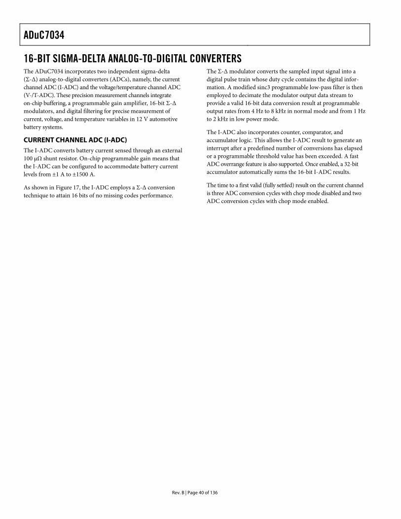
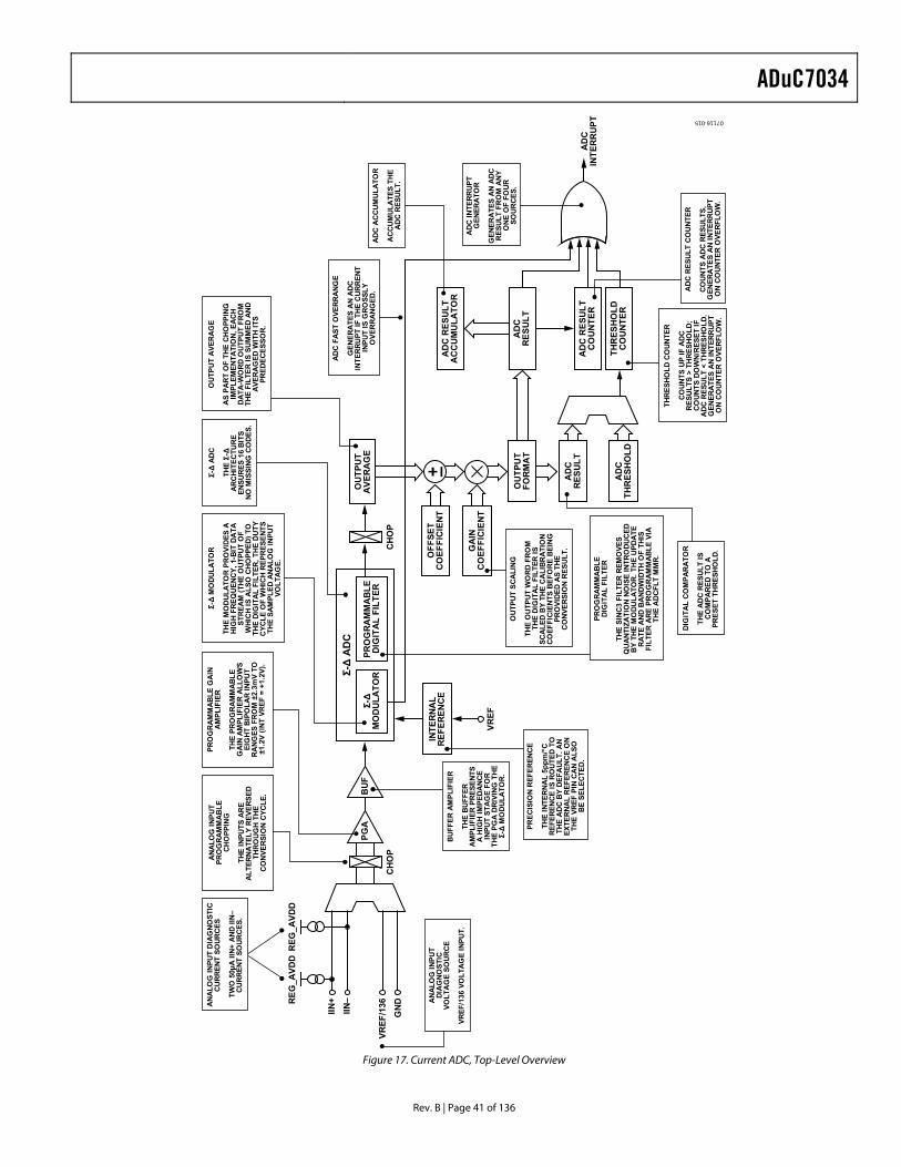
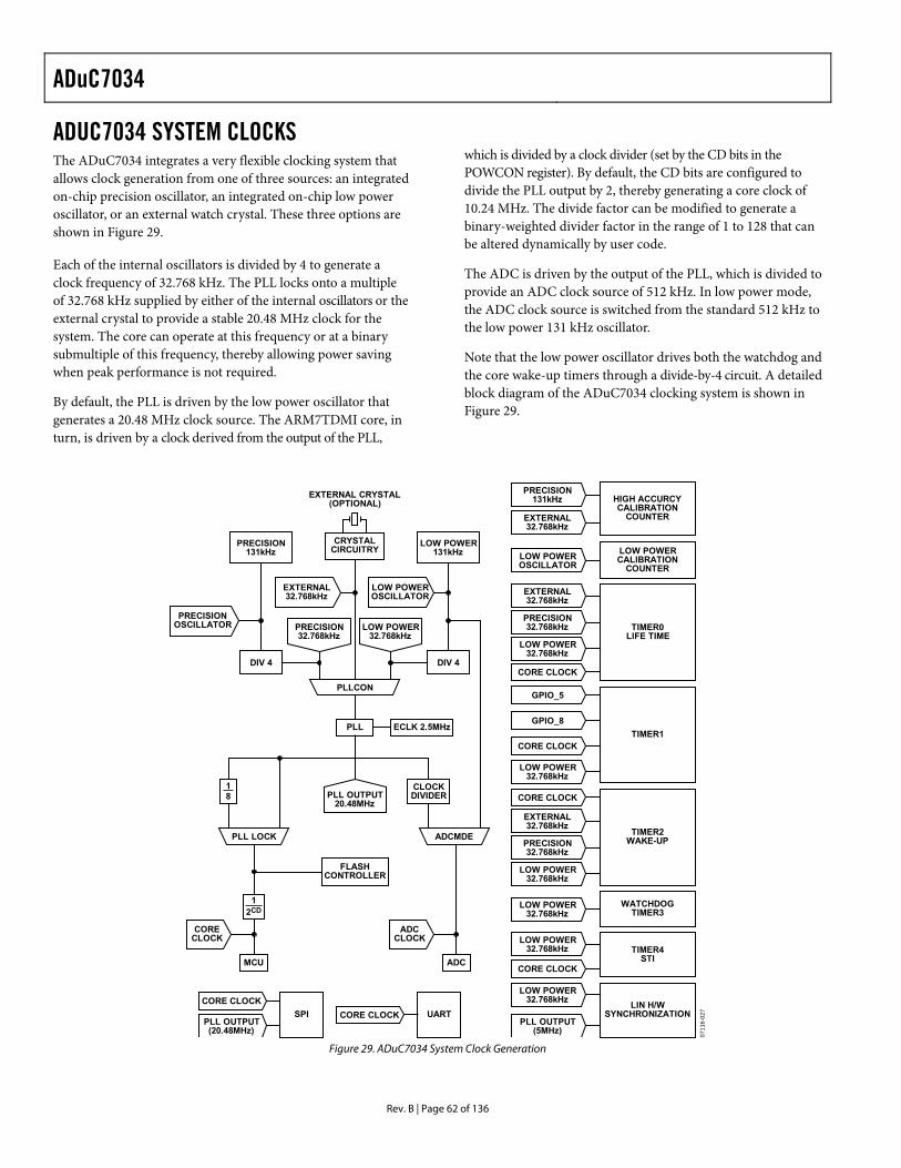
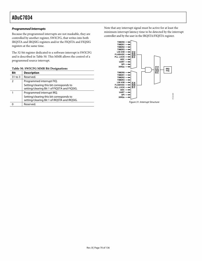
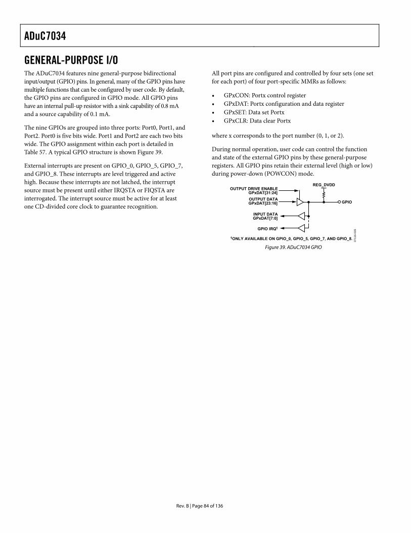
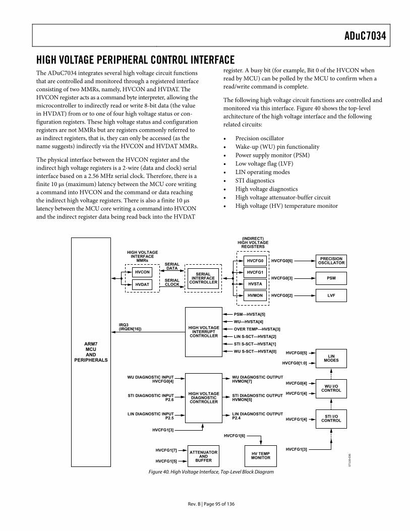
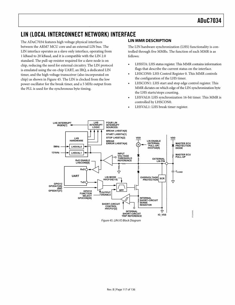
THEORY OF OPERATION The ADuC7034 is a complete system solution for battery monitoring in 12 V automotive applications. This device integrates all of the required features to precisely and intelligently monitor, process, and diagnose 12 V battery parameters, including battery current, voltage, and temperature, over a wide range of operating conditions.
Minimizing external system components, the device is powered directly from the 12 V battery. An on-chip low dropout regula-tor generates the supply voltage for two integrated 16-bit Σ-Δ ADCs. The ADCs precisely measure battery current, voltage, and temperature to characterize the state of health and state of charge of the car battery.
A Flash/EE memory-based ARM7™ microcontroller (MCU) is also integrated on chip. It is used both to preprocess the acquired battery variables and to manage communication from the ADuC7034 to the main electronic control unit (ECU) via a local interconnect network (LIN) interface that is integrated on chip.
Both the MCU and the ADC subsystem can be individually configured to operate in normal or flexible power-saving modes of operation.
In its normal operating mode, the MCU is clocked indirectly from an on-chip oscillator via the phase-locked loop (PLL) at a maximum clock rate of 20.48 MHz. In its power-saving oper-ating modes, the MCU can be totally powered down, waking up only in response to an ADC conversion result being ready, a digital comparator event, a wake-up timer event, a power-on rest (POR) event, or an external serial communication event.
The ADC can be configured to operate in a normal (full power) mode of operation, interrupting the MCU after various sample conversion events. The current channel features two low power modes—low power mode and low power plus mode—that generate conversion results to a lower performance specification.
On-chip factory firmware supports in-circuit Flash/EE repro-gramming via the LIN or JTAG serial interface ports, and nonintrusive emulation is also supported via the JTAG interface. These features are incorporated into a low cost QuickStart™ development system supporting the ADuC7034.
The ADuC7034 operates directly from the 12 V battery supply and is fully specified over a temperature range of −40°C to +115°C. The ADuC7034 is functional but has degraded performance at temperatures from 115°C to 125°C.
OVERVIEW OF THE ARM7TDMI CORE The ARM7 core is a 32-bit reduced instruction set computer (RISC) developed by ARM Ltd. The ARM7TDMI is a von Neumann-based architecture, meaning that it uses a single 32-bit bus for instruction and data. The length of the data can be 8, 16, or 32 bits, and the length of the instruction word can
be either 16 bits or 32 bits, depending on the mode in which the core is operating.
The ARM7TDMI is an ARM7 core with four additional features, as listed in Table 8.
Table 8. ARM7TDMI Feature Description T Support for the Thumb® (16-bit) instruction set D Support for debug M Enhanced multiplier I Includes the EmbeddedICE™ module to support
embedded system debugging
Thumb Mode (T)
An ARM instruction is 32 bits long. The ARM7TDMI processor supports a second instruction set, called the Thumb instruction set, which is compressed into 16 bits. Faster code execution from 16-bit memory and greater code density can be achieved by using the Thumb instruction set; therefore, the ARM7TDMI core is particularly suited for embedded applications.
However, the Thumb mode has three limitations:
• Relative to ARM, the Thumb code usually requires more instructions to perform a task. Therefore, ARM code is best for maximizing the performance of time-critical code in most applications.
• The Thumb instruction set does not include some instruct-tions that are needed for exception handling; therefore, ARM code may be required for exception handling.
• When an interrupt occurs, the core vectors to the interrupt location in memory and executes the code present at that address. The first command is required to be in ARM code.
Multiplier (M)
The ARM7TDMI instruction set includes an enhanced multiplier with four extra instructions to perform 32-bit × 32-bit multiplication with a 64-bit result, or 32-bit × 32-bit multiplication-accumulation (MAC) with a 64-bit result.
EmbeddedICE (I)
The EmbeddedICE module provides integrated on-chip debug support for the ARM7TDMI. The EmbeddedICE module contains the breakpoint and watchpoint registers that allow nonintrusive user code debugging. These registers are con-trolled through the JTAG test port. When a breakpoint or watchpoint is encountered, the processor halts and enters the debug state. When in the debug state, the processor registers can be interrogated, as can the Flash/EE, SRAM, and memory-mapped registers.
ADuC7034
Rev. B | Page 21 of 136
ARM7 Exceptions
The ARM7 supports five types of exceptions, with a privileged processing mode associated with each type. The five types of exceptions are as follows:
• Normal interrupt (IRQ). This is provided to service general-purpose interrupt handling of internal and external events.
• Fast interrupt (FIQ). This is provided to service a data transfer or a communication channel with low latency. FIQ has priority over IRQ.
• Memory abort (prefetch and data). • Attempted execution of an undefined instruction. • Software interrupt (SWI) instruction. This can be used to
make a call to an operating system.
Typically, the programmer defines interrupts as IRQ, but for higher priority interrupts, the programmer can define interrupts as the FIQ type.
The priority of these exceptions and vector address are listed in Table 9.
Table 9. Exception Priorities and Vector Addresses Priority Exception Address 1 Hardware reset 0x00 2 Memory abort (data) 0x10 3 FIQ 0x1C 4 IRQ 0x18 5 Memory abort (prefetch) 0x0C 6 Software interrupt1 0x08 6 Undefined instruction1 0x04 1 A software interrupt and an undefined instruction exception have the same
priority and are mutually exclusive.
The vectors for the exception modes listed in Table 9 are located at Address 0x00 to Address 0x1C, with a reserved regis- ter at Address 0x14. Location 0x14 must be written as either 0x27011970 or the checksum of Page 0 (excluding Location 0x14); otherwise, user code does not execute and LIN download mode is entered.
ARM Registers
The ARM7TDMI has 16 standard registers. R0 to R12 are used for data manipulation, R13 is the stack pointer, R14 is the link register, and R15 is the program counter that indicates the instruction currently being executed. The link register contains the address from which the user has branched (if the branch and link command was used) or the command during which an exception occurred.
The stack pointer contains the current location of the stack. As a general rule, on an ARM7TDMI the stack starts at the top of the available RAM area and descends, using the area as required. A separate stack is defined for each of the exceptions. The size of each stack is user configurable and is dependent on the target application. On the ADuC7034, the stack begins at 0x00040FFC and then descends. When programming using high-level languages, such as C, it is necessary to ensure that the stack does not overflow. This is dependent on the performance of the compiler that is used.
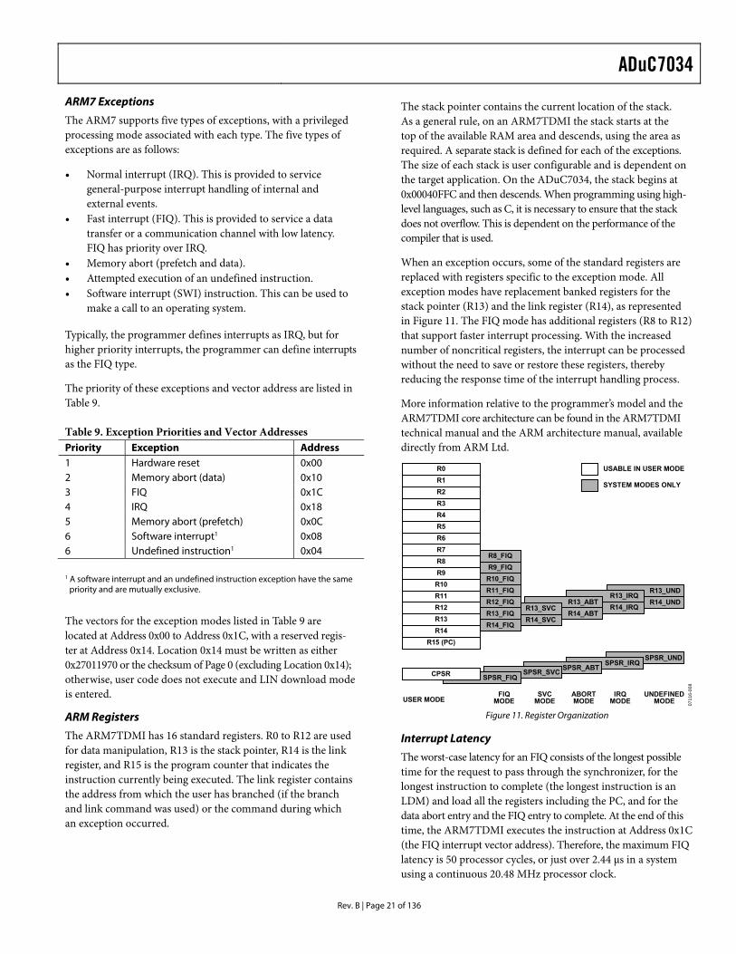
When an exception occurs, some of the standard registers are replaced with registers specific to the exception mode. All exception modes have replacement banked registers for the stack pointer (R13) and the link register (R14), as represented in Figure 11. The FIQ mode has additional registers (R8 to R12) that support faster interrupt processing. With the increased number of noncritical registers, the interrupt can be processed without the need to save or restore these registers, thereby reducing the response time of the interrupt handling process.
More information relative to the programmer’s model and the ARM7TDMI core architecture can be found in the ARM7TDMI technical manual and the ARM architecture manual, available directly from ARM Ltd.
USABLE IN USER MODE
SYSTEM MODES ONLY
SPSR_UNDSPSR_IRQSPSR_ABTSPSR_SVC
R8_FIQR9_FIQ
R10_FIQR11_FIQR12_FIQR13_FIQR14_FIQ
R13_UNDR14_UND
R0R1R2R3R4R5R6R7R8R9R10R11R12R13R14
R15 (PC)
R13_IRQR14_IRQ
R13_ABTR14_ABT
R13_SVCR14_SVC
SPSR_FIQCPSR
USER MODEFIQ
MODESVC
MODEABORTMODE
IRQMODE
UNDEFINEDMODE 07
116-
008
Figure 11. Register Organization
Interrupt Latency
The worst-case latency for an FIQ consists of the longest possible time for the request to pass through the synchronizer, for the longest instruction to complete (the longest instruction is an LDM) and load all the registers including the PC, and for the data abort entry and the FIQ entry to complete. At the end of this time, the ARM7TDMI executes the instruction at Address 0x1C (the FIQ interrupt vector address). Therefore, the maximum FIQ latency is 50 processor cycles, or just over 2.44 μs in a system using a continuous 20.48 MHz processor clock.
ADuC7034
Rev. B | Page 22 of 136
The maximum IRQ latency can be similarly calculated, but must allow for the fact that FIQ has higher priority and may delay entry into the IRQ handling routine for an arbitrary length of time. This time can be reduced to 42 cycles if the LDM command is not used; some compilers have an option to compile without using this command. Another option is to run the part in Thumb mode, which reduces the time to 22 cycles.
The minimum latency for a FIQ or IRQ is five cycles. This consists of the shortest time for the request to pass through the synchronizer plus the time to enter the exception mode.
Note that the ARM7TDMI initially (first instruction) runs in ARM (32-bit) mode when an exception occurs. The user can immediately switch from ARM mode to Thumb mode if required, for example, when executing interrupt service routines.
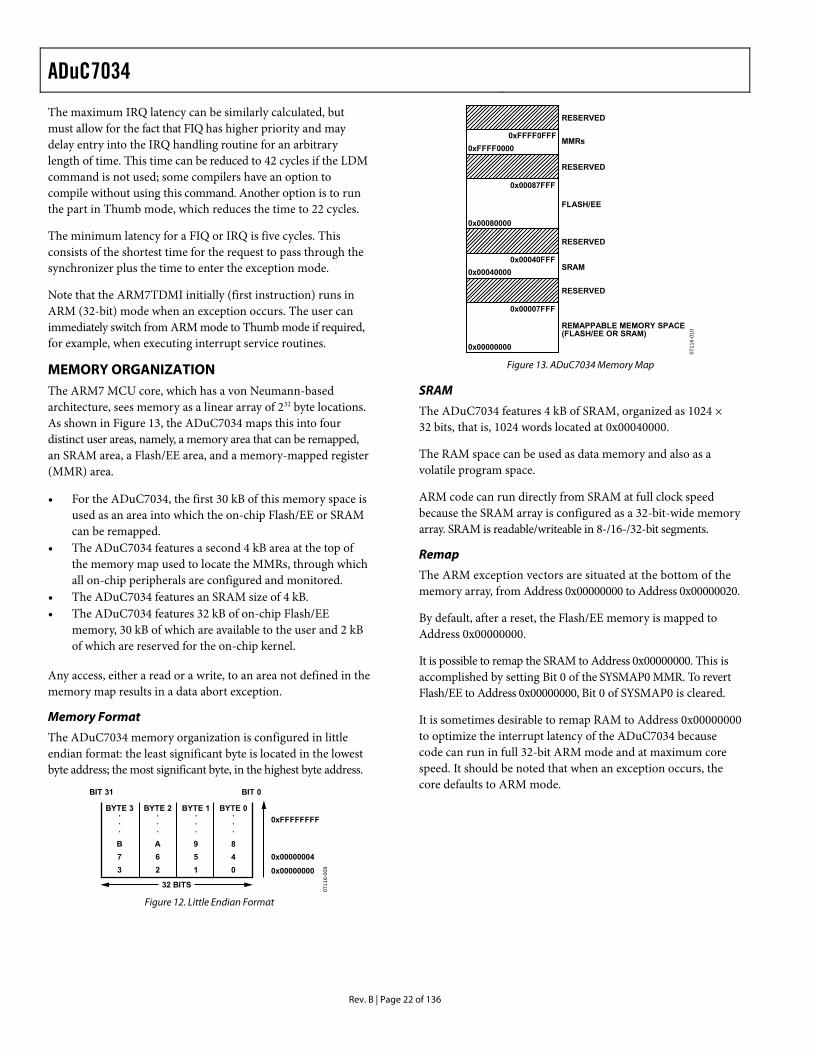
MEMORY ORGANIZATION The ARM7 MCU core, which has a von Neumann-based architecture, sees memory as a linear array of 232 byte locations. As shown in Figure 13, the ADuC7034 maps this into four distinct user areas, namely, a memory area that can be remapped, an SRAM area, a Flash/EE area, and a memory-mapped register (MMR) area.
• For the ADuC7034, the first 30 kB of this memory space is used as an area into which the on-chip Flash/EE or SRAM can be remapped.
• The ADuC7034 features a second 4 kB area at the top of the memory map used to locate the MMRs, through which all on-chip peripherals are configured and monitored.
• The ADuC7034 features an SRAM size of 4 kB. • The ADuC7034 features 32 kB of on-chip Flash/EE
memory, 30 kB of which are available to the user and 2 kB of which are reserved for the on-chip kernel.
Any access, either a read or a write, to an area not defined in the memory map results in a data abort exception.
Memory Format
The ADuC7034 memory organization is configured in little endian format: the least significant byte is located in the lowest byte address; the most significant byte, in the highest byte address.
BIT 31
BYTE 2
A62
.
.
.
BYTE 3
B73
.
.
.
BYTE 1
951
.
.
.
BYTE 0
840
.
.
.
BIT 0
32 BITS
0xFFFFFFFF
0x00000004
0x00000000
0711
6-00
9
Figure 12. Little Endian Format
0x00040FFF0x00040000
0xFFFF0FFF0xFFFF0000
MMRs
0x00087FFF
0x00080000
FLASH/EE
SRAM
0x00007FFF
0x00000000
REMAPPABLE MEMORY SPACE(FLASH/EE OR SRAM)
RESERVED
RESERVED
RESERVED
RESERVED
0711
6-01
0
Figure 13. ADuC7034 Memory Map
SRAM
The ADuC7034 features 4 kB of SRAM, organized as 1024 × 32 bits, that is, 1024 words located at 0x00040000.
The RAM space can be used as data memory and also as a volatile program space.
ARM code can run directly from SRAM at full clock speed because the SRAM array is configured as a 32-bit-wide memory array. SRAM is readable/writeable in 8-/16-/32-bit segments.
Remap
The ARM exception vectors are situated at the bottom of the memory array, from Address 0x00000000 to Address 0x00000020.
By default, after a reset, the Flash/EE memory is mapped to Address 0x00000000.
It is possible to remap the SRAM to Address 0x00000000. This is accomplished by setting Bit 0 of the SYSMAP0 MMR. To revert Flash/EE to Address 0x00000000, Bit 0 of SYSMAP0 is cleared.
It is sometimes desirable to remap RAM to Address 0x00000000 to optimize the interrupt latency of the ADuC7034 because code can run in full 32-bit ARM mode and at maximum core speed. It should be noted that when an exception occurs, the core defaults to ARM mode.
ADuC7034
Rev. B | Page 23 of 136
Remap Operation
When a reset occurs on the ADuC7034, execution starts automatically in the factory-programmed internal configuration code. This so-called kernel is hidden and cannot be accessed by user code. If the ADuC7034 is in normal mode, it executes the power-on configuration routine of the kernel and then jumps to the reset vector, Address 0x00000000, to execute the user’s reset exception routine. Because the Flash/EE is mirrored at the bottom of the memory array at reset, the reset routine must always be written in Flash/EE.
The remap command must be executed from the absolute Flash/EE address, not from the mirrored, remapped segment of memory, which may be replaced by SRAM. If a remap operation is executed while operating code from the mirrored location, prefetch/data aborts may occur or the user may observe abnormal program operation.
Any kind of reset remaps the Flash/EE memory to the bottom of the memory array.
SYSMAP0 Register
Name: SYSMAP0
Address: 0xFFFF0220
Default Value: Updated by the kernel
Access: Read/write access
Function: This 8-bit register allows user code to remap either RAM or Flash/EE space into the bottom of the ARM memory space, starting at Address 0x00000000.
Table 10. SYSMAP0 MMR Bit Designations Bit Description 7 to 1 Reserved. These bits are reserved and should
be written as 0 by user code. 0 Remap bit. Set by the user to remap the SRAM to
Address 0x00000000. Cleared automatically after a reset to remap
the Flash/EE memory to Address 0x00000000.
ADuC7034
Rev. B | Page 24 of 136
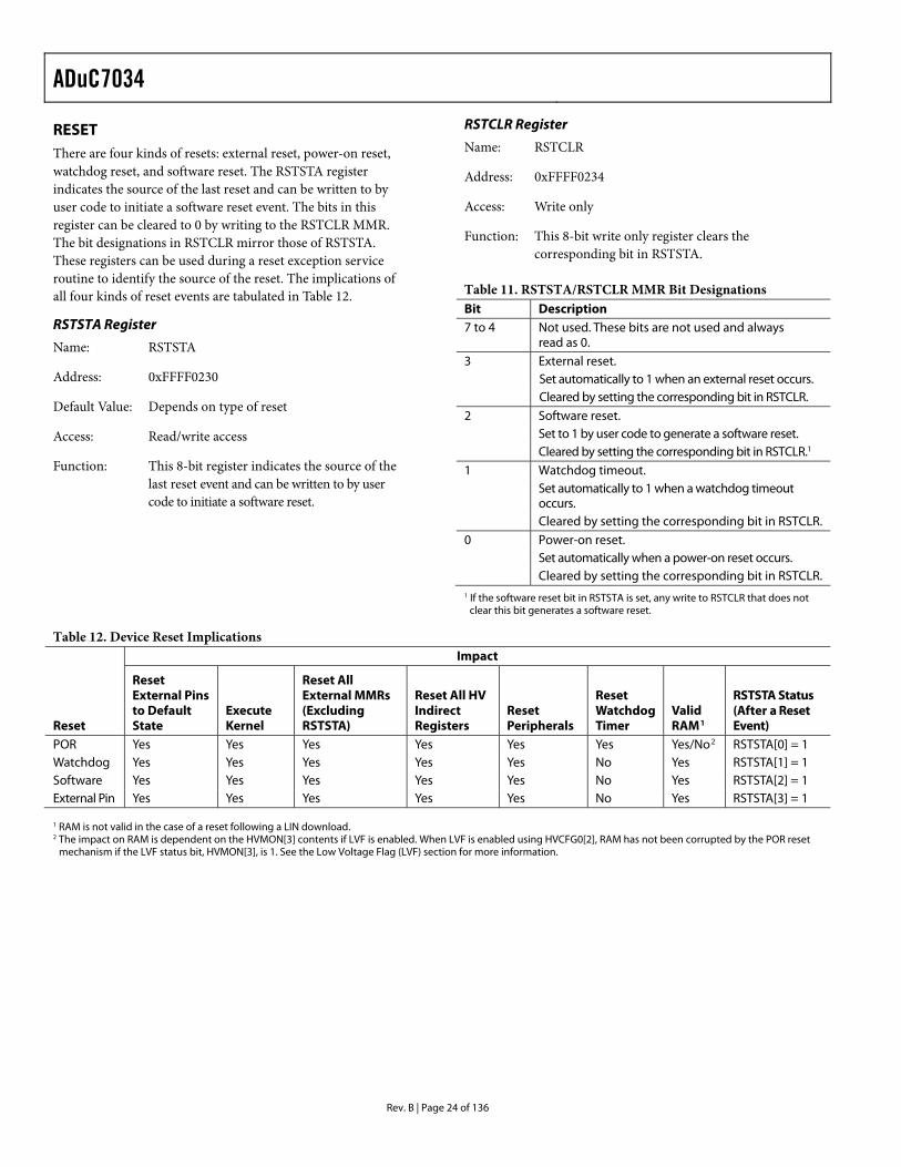
RESET There are four kinds of resets: external reset, power-on reset, watchdog reset, and software reset. The RSTSTA register indicates the source of the last reset and can be written to by user code to initiate a software reset event. The bits in this register can be cleared to 0 by writing to the RSTCLR MMR. The bit designations in RSTCLR mirror those of RSTSTA. These registers can be used during a reset exception service routine to identify the source of the reset. The implications of all four kinds of reset events are tabulated in Table 12.
RSTSTA Register
Name: RSTSTA
Address: 0xFFFF0230
Default Value: Depends on type of reset
Access: Read/write access
Function: This 8-bit register indicates the source of the last reset event and can be written to by user code to initiate a software reset.
RSTCLR Register
Name: RSTCLR
Address: 0xFFFF0234
Access: Write only
Function: This 8-bit write only register clears the corresponding bit in RSTSTA.
Table 11. RSTSTA/RSTCLR MMR Bit Designations Bit Description 7 to 4 Not used. These bits are not used and always
read as 0. 3 External reset. Set automatically to 1 when an external reset occurs. Cleared by setting the corresponding bit in RSTCLR. 2 Software reset. Set to 1 by user code to generate a software reset. Cleared by setting the corresponding bit in RSTCLR.1 1 Watchdog timeout. Set automatically to 1 when a watchdog timeout
occurs. Cleared by setting the corresponding bit in RSTCLR. 0 Power-on reset. Set automatically when a power-on reset occurs. Cleared by setting the corresponding bit in RSTCLR. 1 If the software reset bit in RSTSTA is set, any write to RSTCLR that does not
clear this bit generates a software reset.
Table 12. Device Reset Implications Impact
Reset
Reset External Pins to Default State
Execute Kernel
Reset All External MMRs (Excluding RSTSTA)
Reset All HV Indirect Registers
Reset Peripherals
Reset Watchdog Timer
Valid RAM1
RSTSTA Status (After a Reset Event)
POR Yes Yes Yes Yes Yes Yes Yes/No2 RSTSTA[0] = 1 Watchdog Yes Yes Yes Yes Yes No Yes RSTSTA[1] = 1 Software Yes Yes Yes Yes Yes No Yes RSTSTA[2] = 1 External Pin Yes Yes Yes Yes Yes No Yes RSTSTA[3] = 1 1 RAM is not valid in the case of a reset following a LIN download. 2 The impact on RAM is dependent on the HVMON[3] contents if LVF is enabled. When LVF is enabled using HVCFG0[2], RAM has not been corrupted by the POR reset
mechanism if the LVF status bit, HVMON[3], is 1. See the Low Voltage Flag (LVF) section for more information.
ADuC7034
Rev. B | Page 25 of 136
FLASH/EE MEMORY The ADuC7034 incorporates Flash/EE memory technology on chip to provide the user with nonvolatile, in-circuit reprogrammable memory space.
Like EEPROM, Flash memory can be programmed in-system at a byte level, although it must first be erased, with the erasure being performed in page blocks. Therefore, Flash memory is often and more correctly referred to as Flash/EE memory.
Overall, Flash/EE memory represents a step closer to the ideal memory device that includes nonvolatility, in-circuit program-mability, high density, and low cost. Incorporated within the ADuC7034, Flash/EE memory technology allows the user to update program code space in-circuit without the need to replace one-time programmable (OTP) devices at remote operating nodes.
The Flash/EE memory is physically located at Address 0x80000. Upon a hard reset, the Flash/EE memory maps to Address 0x00000000. The factory-set default contents of all Flash/EE memory locations is 0xFF. Flash/EE can be read in 8-/16-/32-bit segments and written in segments of 16 bits. The Flash/EE is rated for 10,000 endurance cycles. This rating is based on the number of times that each byte is cycled, that is, erased and programmed. Implementing a redundancy scheme in the software ensures greater than 10,000 endurance cycles.
The user can also write data variables to the Flash/EE memory during run-time code execution, for example, for storing diagnostic battery parameter data.
The entire Flash/EE is available to the user as code and non-volatile data memory. There is no distinction between data space and program space during ARM code processing. The real width of the Flash/EE memory is 16 bits, meaning that in ARM mode (32-bit instruction), two accesses to the Flash/EE are necessary for each instruction fetch. When operating at speeds of less than 20.48 MHz, the Flash/EE memory controller can transparently fetch the second 16-bit halfword (part of the 32-bit ARM operation code) within a single core clock period. Therefore, for speeds less than 20.48 MHz (that is, CD > 0), it is recommended to use ARM mode. For 20.48 MHz operation (that is, CD = 0), it is recommended to operate in Thumb mode.
The page size of this Flash/EE memory is 512 bytes. Typically, it takes the Flash/EE controller 20 ms to erase a page, regardless of CD. Writing a 16-bit word at CD = 0, 1, 2, or 3 requires 50 μs; at CD = 4 or 57, 0 μs; at CD = 6, 80 μs; and at CD = 7, 105 μs.
It is possible to write to a single 16-bit location only twice between erasures; that is, it is possible to walk bytes, not bits. If a location is written to more than twice, the contents of the Flash/EE page may become corrupt.
PROGRAMMING FLASH/EE MEMORY IN-CIRCUIT The Flash/EE memory can be programmed in-circuit, using a serial download mode via the LIN interface or the integrated JTAG port.
Serial Downloading (In-Circuit Programming)
The ADuC7034 facilitates code download via the LIN pin.
JTAG Access
The ADuC7034 features an on-chip JTAG debug port to facilitate code downloading and debugging.
ADuC7034 Flash/EE Memory
The total 32 kB of Flash/EE is organized as 15,000 × 16 bits. Of this total, 30 kB are user space and 2 kB are reserved for boot loader/kernel space.
FLASH/EE CONTROL INTERFACE Access to and control of the Flash/EE memory on the ADuC7034 is managed by an on-chip memory controller. The controller manages the Flash/EE memory as a single block of 32 kB.
It should be noted that the MCU core is halted until the command completes. User software must ensure that the Flash/EE controller completes any erase or write cycle before the PLL is powered down. If the PLL is powered down before an erase or write cycle is completed, the Flash/EE page may become corrupt. User code, LIN, and JTAG programming use the Flash/EE control interface, consisting of the following MMRs:
• FEE0STA: read only register. Reflects the status of the Flash/EE control interface.
• FEE0MOD: sets the operating mode of the Flash/EE control interface.
• FEE0CON: 8-bit command register. The commands are interpreted as described in Table 13.
• FEE0DAT: 16-bit data register. • FEE0ADR: 16-bit address register. • FEE0SIG: holds the 24-bit code signature as a result of the
signature command being initiated. • FEE0HID: protection MMR. Controls read and write
protection of the Flash/EE memory code space. If previously configured via the FEE0PRO register, FEE0HID may require a software key to enable access.
• FEE0PRO: a buffer of the FEE0HID register. Stores the FEE0HID value and therefore automatically downloads to the FEE0HID registers on subsequent reset and power-on events.
The FEE0CON Register to FEE0DAT Register sections provide detailed descriptions of the bit designations for each of the Flash/EE control MMRs.
ADuC7034
Rev. B | Page 26 of 136
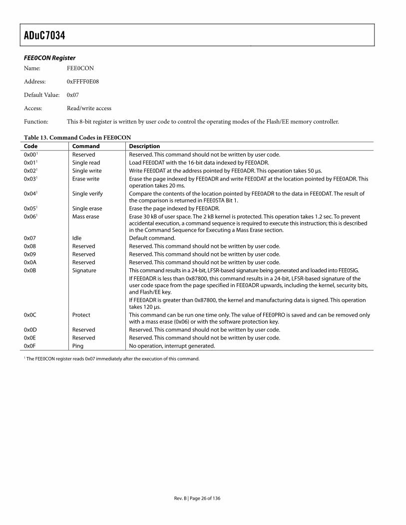
FEE0CON Register
Name: FEE0CON
Address: 0xFFFF0E08
Default Value: 0x07
Access: Read/write access
Function: This 8-bit register is written by user code to control the operating modes of the Flash/EE memory controller.
Table 13. Command Codes in FEE0CON Code Command Description 0x001 Reserved Reserved. This command should not be written by user code. 0x011 Single read Load FEE0DAT with the 16-bit data indexed by FEE0ADR. 0x021 Single write Write FEE0DAT at the address pointed by FEE0ADR. This operation takes 50 μs. 0x031 Erase write Erase the page indexed by FEE0ADR and write FEE0DAT at the location pointed by FEE0ADR. This
operation takes 20 ms. 0x041 Single verify Compare the contents of the location pointed by FEE0ADR to the data in FEE0DAT. The result of
the comparison is returned in FEE0STA Bit 1. 0x051 Single erase Erase the page indexed by FEE0ADR. 0x061 Mass erase Erase 30 kB of user space. The 2 kB kernel is protected. This operation takes 1.2 sec. To prevent
accidental execution, a command sequence is required to execute this instruction; this is described in the Command Sequence for Executing a Mass Erase section.
0x07 Idle Default command. 0x08 Reserved Reserved. This command should not be written by user code. 0x09 Reserved Reserved. This command should not be written by user code. 0x0A Reserved Reserved. This command should not be written by user code. 0x0B Signature This command results in a 24-bit, LFSR-based signature being generated and loaded into FEE0SIG. If FEE0ADR is less than 0x87800, this command results in a 24-bit, LFSR-based signature of the
user code space from the page specified in FEE0ADR upwards, including the kernel, security bits, and Flash/EE key.
If FEE0ADR is greater than 0x87800, the kernel and manufacturing data is signed. This operation takes 120 μs.
0x0C Protect This command can be run one time only. The value of FEE0PRO is saved and can be removed only with a mass erase (0x06) or with the software protection key.
0x0D Reserved Reserved. This command should not be written by user code. 0x0E Reserved Reserved. This command should not be written by user code. 0x0F Ping No operation, interrupt generated. 1 The FEE0CON register reads 0x07 immediately after the execution of this command.
ADuC7034
Rev. B | Page 27 of 136
Command Sequence for Executing a Mass Erase
Given the significance of the mass erase command, a specific code sequence must be executed to initiate this operation:
1. Set Bit 3 in FEE0MOD. 2. Write 0xFFC3 in FEE0ADR. 3. Write 0x3CFF in FEE0DAT. 4. Run the mass erase command (Code 0x06) in FEE0CON.
This sequence is illustrated in the following example:
FEE0MOD = 0x08; FEE0ADR = 0xFFC3; FEE0DAT = 0x3CFF; FEE0CON = 0x06; //Mass erase command while (FEE0STA & 0x04) //Wait for command to finish
FEE0STA Register
Name: FEE0STA
Address: 0xFFFF0E00
Default Value: 0x20
Access: Read only
Function: This 8-bit, read only register can be read by user code and reflects the current status of the Flash/EE memory controller.
Table 14. FEE0STA MMR Bit Designation Bit Description 7 to 4 Not used. These bits are not used and always read as 0. 3 Flash/EE interrupt status bit. Set automatically when an interrupt occurs, that is,
when a command is complete and the Flash/EE interrupt enable bit in the FEE0MOD register is set.
Cleared automatically when the FEE0STA register is read by user code.
2 Flash/EE controller busy. Set automatically when the Flash/EE controller is busy. Cleared automatically when the controller is not busy. 1 Command fail. Set automatically when a command written to
FEE0CON fails. Cleared automatically when the FEE0STA register is
read by user code. 0 Command successful. Set automatically by MCU when a command is
completed successfully. Cleared automatically when the FEE0STA register is
read by user code.
FEE0MOD Register
Name: FEE0MOD
Address: 0xFFFF0E04
Default Value: 0x00
Access: Read/write access
Function: This register is written by user code to configure the mode of operation of the Flash/EE memory controller.
Table 15. FEE0MOD MMR Bit Designation Bit Description 7 Not used. These bits are reserved for future functionality
and should be written as 0 by user code. 6 to 5 Flash/EE security lock bits. These bits must be written as
[6:5] = 10 to complete the Flash/EE security protect sequence.
4 Flash/EE controller command complete interrupt enable. Set to 1 by user code to enable the Flash/EE controller
to generate an interrupt upon completion of a Flash/EE command.
Cleared to disable the generation of a Flash/EE interrupt upon completion of a Flash/EE command.
3 Flash/EE erase/write enable. Set by user code to enable the Flash/EE erase and write
access via FEE0CON. Cleared by user code to disable the Flash/EE erase and
write access via FEE0CON. 2 Reserved. 1 Flash/EE controller abort enable. Set to 1 by user code to enable the Flash/EE controller
abort functionality. Cleared by user code to disable the Flash/EE controller
abort functionality. 0 Reserved.
FEE0ADR Registers
Name: FEE0ADR
Address: 0xFFFF0E10
Default Value: Nonzero, see the
System Identification Register section
Access: Read/write access
Function: This 16-bit register dictates the address acted upon when a Flash/EE command is executed via FEE0CON.
ADuC7034
Rev. B | Page 28 of 136
FEE0DAT Register
Name: FEE0DAT
Address: 0xFFFF0E0C
Default Value: 0x0000
Access: Read/write access
Function: This 16-bit register contains the data either read from or to be written to the Flash/EE memory.
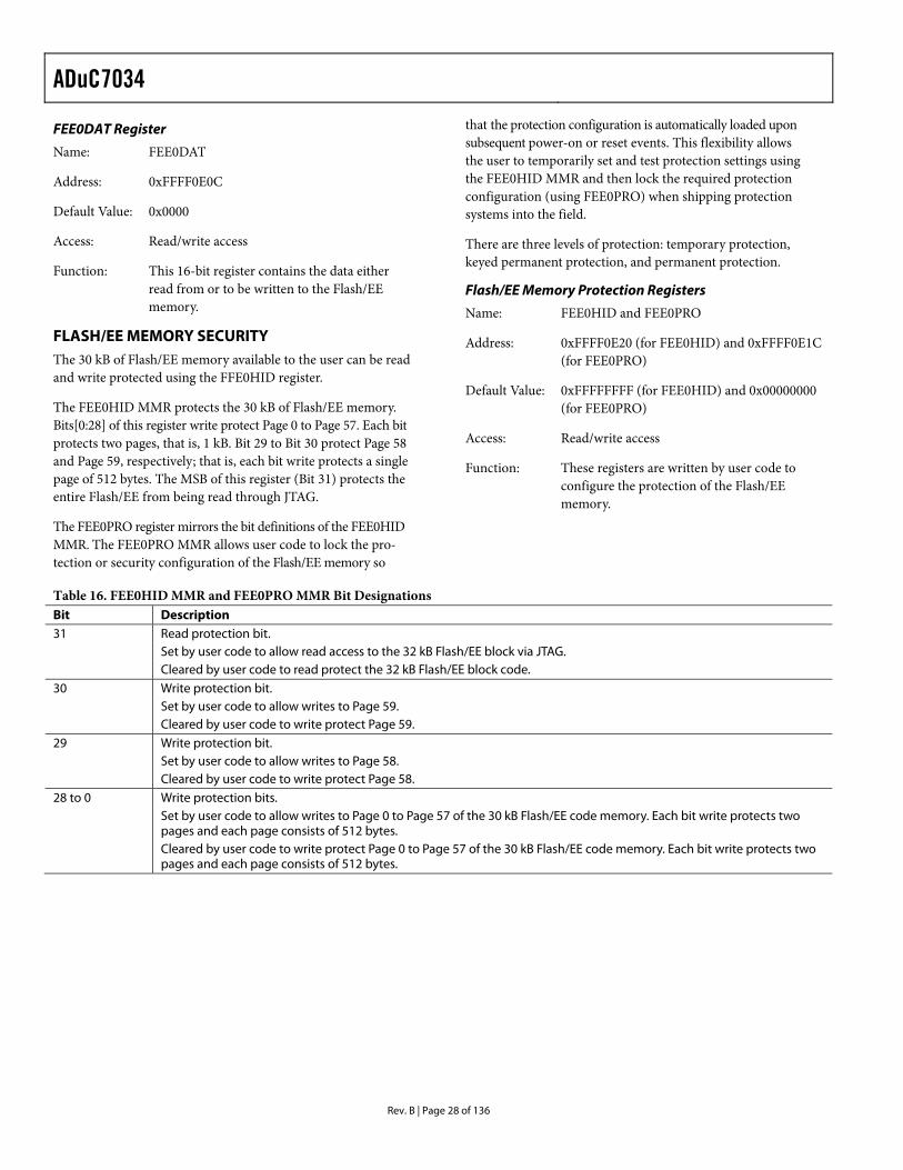
FLASH/EE MEMORY SECURITY The 30 kB of Flash/EE memory available to the user can be read and write protected using the FFE0HID register.
The FEE0HID MMR protects the 30 kB of Flash/EE memory. Bits[0:28] of this register write protect Page 0 to Page 57. Each bit protects two pages, that is, 1 kB. Bit 29 to Bit 30 protect Page 58 and Page 59, respectively; that is, each bit write protects a single page of 512 bytes. The MSB of this register (Bit 31) protects the entire Flash/EE from being read through JTAG.
The FEE0PRO register mirrors the bit definitions of the FEE0HID MMR. The FEE0PRO MMR allows user code to lock the pro-tection or security configuration of the Flash/EE memory so
that the protection configuration is automatically loaded upon subsequent power-on or reset events. This flexibility allows the user to temporarily set and test protection settings using the FEE0HID MMR and then lock the required protection configuration (using FEE0PRO) when shipping protection systems into the field.
There are three levels of protection: temporary protection, keyed permanent protection, and permanent protection.
Flash/EE Memory Protection Registers
Name: FEE0HID and FEE0PRO
Address: 0xFFFF0E20 (for FEE0HID) and 0xFFFF0E1C (for FEE0PRO)
Default Value: 0xFFFFFFFF (for FEE0HID) and 0x00000000 (for FEE0PRO)
Access: Read/write access
Function: These registers are written by user code to configure the protection of the Flash/EE memory.
Table 16. FEE0HID MMR and FEE0PRO MMR Bit Designations Bit Description 31 Read protection bit. Set by user code to allow read access to the 32 kB Flash/EE block via JTAG. Cleared by user code to read protect the 32 kB Flash/EE block code. 30 Write protection bit. Set by user code to allow writes to Page 59. Cleared by user code to write protect Page 59. 29 Write protection bit. Set by user code to allow writes to Page 58. Cleared by user code to write protect Page 58. 28 to 0 Write protection bits. Set by user code to allow writes to Page 0 to Page 57 of the 30 kB Flash/EE code memory. Each bit write protects two
pages and each page consists of 512 bytes. Cleared by user code to write protect Page 0 to Page 57 of the 30 kB Flash/EE code memory. Each bit write protects two
pages and each page consists of 512 bytes.
ADuC7034
Rev. B | Page 29 of 136
Temporary Protection
Temporary protection can be set and removed by writing directly into the FEE0HID MMR. This register is volatile and, therefore, protection is only in place for as long as the part remains powered on. The protection setting is not reloaded after a power cycle.
Keyed Permanent Protection
Keyed permanent protection can be set via FEE0PRO to lock the protection configuration. The software key used at the start of the required FEE0PRO write sequence is saved one time only and must be used for any subsequent access of the FEE0HID or FEE0PRO MMRs. A mass erase sets the software protection key back to 0xFFFF but also erases the entire user code space.
Permanent Protection
Permanent protection can be set via FEE0PRO, similar to how keyed permanent protection is set, with the only difference being that the software key used is 0xDEADDEAD. When the FEE0PRO write sequence is saved, only a mass erase sets the software protection key back to 0xFFFFFFFF. This also erases the entire user code space.
Sequence to Write the Software Protection Key and Set Permanent Protection
1. Write in FEE0PRO corresponding to the pages to be protected.
2. Write the new (user-defined) 32-bit software protection key in FEE0ADR (Bits[31:16]) and FEE0DAT (Bits[15:0]).
3. Write 10 in FEE0MOD (Bits[6:5]) and set FEE0MOD (Bit 3). 4. Run the protect command (Code 0x0C) in FEE0CON.
To remove or modify the protection, the same sequence can be used with a modified value of FEE0PRO.
The previous sequence for writing the key and setting perma-nent protection is illustrated in the following example, this protects writing Page 4 and Page 5 of the Flash/EE:
Int a = FEE0STA; // Ensure FEE0STA is cleared FEE0PRO = 0xFFFFFFFB; // Protect Page 4 and Page 5 FEE0ADR = 0x66BB; // 32-bit key value (Bits[31:16]) FEE0DAT = 0xAA55; // 32-bit key value (Bits[15:0]) FEE0MOD = 0x0048 // Lock security sequence FEE0CON = 0x0C; // Write key command while (FEE0STA & 0x04) // Wait for command to finish
FLASH/EE MEMORY RELIABILITY The Flash/EE memory array on the part is fully qualified for two key Flash/EE memory characteristics: Flash/EE memory cycling endurance and Flash/EE memory data retention.
Endurance quantifies the ability of the Flash/EE memory to be cycled through many program, read, and erase cycles. A single endurance cycle is composed of four independent, sequential events, defined as
• Initial page erase sequence • Read/verify sequence • Byte program sequence • Second read/verify sequence
In reliability qualification, every halfword (16 bits wide) location of the three pages (top, middle, and bottom) in the Flash/EE memory is cycled 10,000 times from 0x0000 to 0xFFFF. As indicated in Table 1, the Flash/EE memory endurance qualification of the part is carried out in accordance with JEDEC Retention Lifetime Specification A117. The results allow the specification of a minimum endurance figure over supply and temperature of 10,000 cycles.
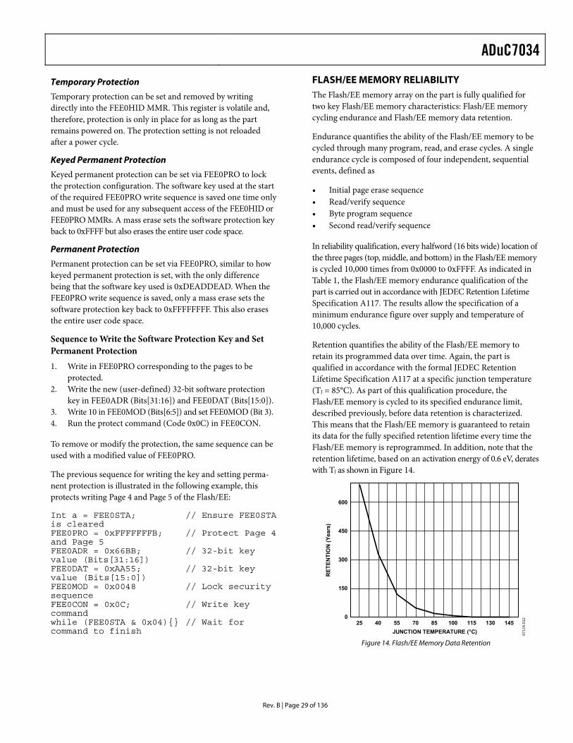
Retention quantifies the ability of the Flash/EE memory to retain its programmed data over time. Again, the part is qualified in accordance with the formal JEDEC Retention Lifetime Specification A117 at a specific junction temperature (TJ = 85°C). As part of this qualification procedure, the Flash/EE memory is cycled to its specified endurance limit, described previously, before data retention is characterized. This means that the Flash/EE memory is guaranteed to retain its data for the fully specified retention lifetime every time the Flash/EE memory is reprogrammed. In addition, note that the retention lifetime, based on an activation energy of 0.6 eV, derates with TJ as shown in Figure 14.
0
150
300
450
600
25 40 55 70 85 100 115 130 145
RET
ENTI
ON
(Yea
rs)
JUNCTION TEMPERATURE (°C) 0711
6-01
2
Figure 14. Flash/EE Memory Data Retention
ADuC7034
Rev. B | Page 30 of 136
CODE EXECUTION TIME FROM SRAM AND FLASH/EE This section describes SRAM and Flash/EE access times during execution for applications where execution time is critical.
Execution from SRAM
Fetching instructions from SRAM takes one clock cycle because the access time of the SRAM is 2 ns, and a clock cycle is 49 ns minimum. However, when the instruction involves reading or writing data to memory, one extra cycle must be added if the data is in SRAM. If the data is in Flash/EE, two cycles must be added: one cycle to execute the instruction and two cycles to retrieve the 32-bit data from Flash/EE. A control flow instruction, such as a branch instruction, takes one cycle to fetch and two cycles to fill the pipeline with the new instructions.
Execution from Flash/EE
In Thumb mode, where instructions are 16 bits, one cycle is needed to fetch any instruction.
In ARM mode with CD = 0, two cycles are needed to fetch the 32-bit instructions. With CD > 0, no extra cycles are required for the fetch because the Flash/EE memory continues to be clocked at full speed. In addition, some dead time is needed before accessing data for any value of CD bits.
Timing is identical in both modes when executing instructions that involve using the Flash/EE for data memory. If the instruction to be executed is a control flow instruction, an extra cycle is needed to decode the new address of the program counter, and then four cycles are needed to fill the pipeline if CD = 0.
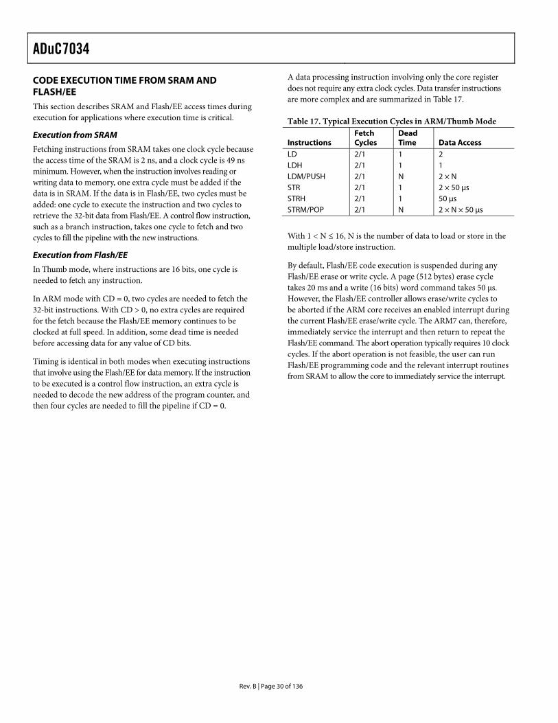
A data processing instruction involving only the core register does not require any extra clock cycles. Data transfer instructions are more complex and are summarized in Table 17.
Table 17. Typical Execution Cycles in ARM/Thumb Mode
Instructions Fetch Cycles
Dead Time Data Access
LD 2/1 1 2 LDH 2/1 1 1 LDM/PUSH 2/1 N 2 × N STR 2/1 1 2 × 50 μs STRH 2/1 1 50 μs STRM/POP 2/1 N 2 × N × 50 μs
With 1 < N ≤ 16, N is the number of data to load or store in the multiple load/store instruction.
By default, Flash/EE code execution is suspended during any Flash/EE erase or write cycle. A page (512 bytes) erase cycle takes 20 ms and a write (16 bits) word command takes 50 μs. However, the Flash/EE controller allows erase/write cycles to be aborted if the ARM core receives an enabled interrupt during the current Flash/EE erase/write cycle. The ARM7 can, therefore, immediately service the interrupt and then return to repeat the Flash/EE command. The abort operation typically requires 10 clock cycles. If the abort operation is not feasible, the user can run Flash/EE programming code and the relevant interrupt routines from SRAM to allow the core to immediately service the interrupt.
ADuC7034
Rev. B | Page 31 of 136
ADuC7034 KERNEL The ADuC7034 features an on-chip kernel resident in the top 2 kB of the Flash/EE code space. After any reset event, this kernel copies the factory-calibrated data from the manufacturing data space into the various on-chip peripherals. The peripherals calibrated by the kernel are as follows:
• Power supply monitor (PSM) • Precision oscillator • Low power oscillator • REG_AVDD/REG_DVDD • Low power voltage reference • Normal mode voltage reference • Current ADC (offset and gain) • Voltage/temperature ADC (offset and gain)
User MMRs that can be modified by the kernel and differ from their POR default values are as follows:
The ADuC7034 also features an on-chip LIN downloader.
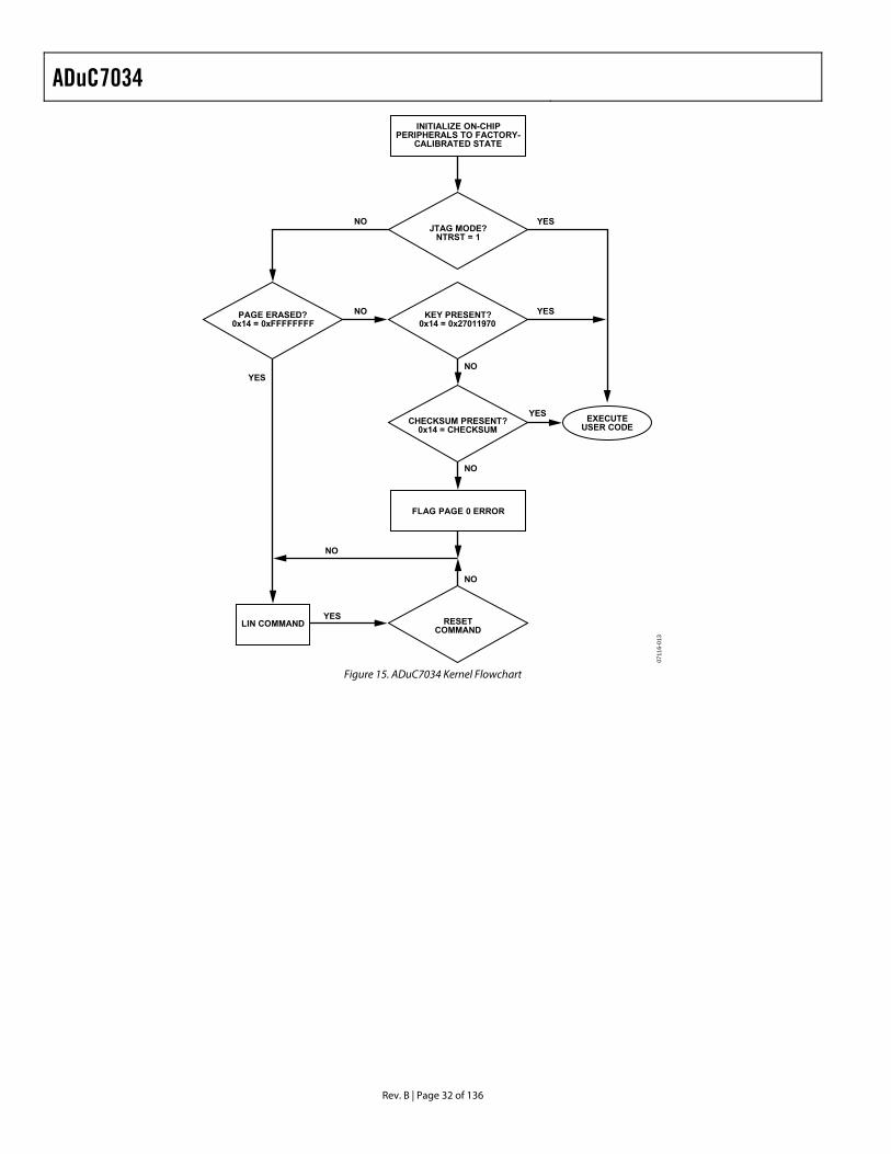
A flow chart of the execution of the kernel is shown in Figure 15. The current revision of the kernel can be derived from SYSSER1, as described in Table 98.
After a POR reset, the watchdog timer is disabled once the kernel code is exited. For the duration of the kernel execution, the watchdog timer is active with a timeout period of 500 ms. This ensures that when an error occurs in the kernel, the ADuC7034 automatically resets. After any other reset, the watchdog timer maintains user code configuration for the period of the kernel and is refreshed just prior to kernel exit. A minimum watchdog period of 30 ms is required to allow correct LIN downloader operation. If LIN download mode is entered, the watchdog is periodically refreshed.
Normal kernel execution time, excluding LIN download, is approximately 5 ms. It is only possible to enter and leave LIN download mode through a reset.
SRAM is not modified during normal kernel execution; rather, SRAM is modified during a LIN download kernel execution.
Note that even with NTRST = 0, user code is not executed unless Address 0x14 contains either 0x27011970 or the checksum of Page 0 excluding Address 0x14. If Address 0x14 does not contain this information, user code is not executed and LIN download mode is entered. During kernel execution, JTAG access is disabled.
With NTRST = 1, user code is always executed.
ADuC7034
Rev. B | Page 32 of 136
INITIALIZE ON-CHIPPERIPHERALS TO FACTORY-
CALIBRATED STATE
FLAG PAGE 0 ERROR
LIN COMMAND
JTAG MODE?NTRST = 1
KEY PRESENT?0x14 = 0x27011970
PAGE ERASED?0x14 = 0xFFFFFFFF
RESETCOMMAND
CHECKSUM PRESENT?0x14 = CHECKSUM
EXECUTEUSER CODE
NO
NO
NO
NO
NO
YES
YES
YES
YES
NO YES
0711
6-01
3
Figure 15. ADuC7034 Kernel Flowchart
ADuC7034
Rev. B | Page 33 of 136
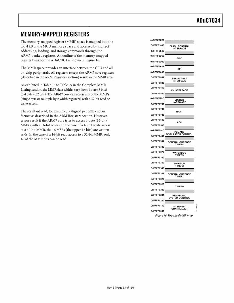
MEMORY-MAPPED REGISTERS The memory-mapped register (MMR) space is mapped into the top 4 kB of the MCU memory space and accessed by indirect addressing, loading, and storage commands through the ARM7-banked registers. An outline of the memory-mapped register bank for the ADuC7034 is shown in Figure 16.
The MMR space provides an interface between the CPU and all on-chip peripherals. All registers except the ARM7 core registers (described in the ARM Registers section) reside in the MMR area.
As exhibited in Table 18 to Table 29 in the Complete MMR Listing section, the MMR data widths vary from 1 byte (8 bits) to 4 bytes (32 bits). The ARM7 core can access any of the MMRs (single byte or multiple byte width registers) with a 32-bit read or write access.
The resultant read, for example, is aligned per little endian format as described in the ARM Registers section. However, errors result if the ARM7 core tries to access 4-byte (32-bit) MMRs with a 16-bit access. In the case of a 16-bit write access to a 32-bit MMR, the 16 MSBs (the upper 16 bits) are written as 0s. In the case of a 16-bit read access to a 32-bit MMR, only 16 of the MMR bits can be read.
FLASH CONTROLINTERFACE
GPIO
SPI
SERIAL TESTINTERFACE
HV INTERFACE
LIN/BSDHARDWARE
UART
ADC
PLL ANDOSCILLATOR CONTROL
GENERAL-PURPOSETIMER4
WATCHDOGTIMER3
WAKE-UPTIMER2
GENERAL-PURPOSETIMER1
TIMER0
REMAP ANDSYSTEM CONTROL
INTERRUPTCONTROLLER
0xFFFFFFFF
0xFFFF1000
0xFFFF0E00
0xFFFF0D50
0xFFFF0D00
0xFFFF0A14
0xFFFF0A00
0xFFFF0894
0xFFFF0880
0xFFFF0810
0xFFFF0800
0xFFFF079C
0xFFFF0780
0xFFFF0730
0xFFFF0700
0xFFFF0580
0xFFFF0500
0xFFFF044C
0xFFFF0400
0xFFFF0394
0xFFFF0380
0xFFFF0370
0xFFFF0360
0xFFFF0350
0xFFFF0340
0xFFFF0334
0xFFFF0320
0xFFFF0318
0xFFFF0300
0xFFFF0244
0xFFFF0220
0xFFFF0110
0xFFFF0000 0711
6-01
4
Figure 16. Top-Level MMR Map
ADuC7034
Rev. B | Page 34 of 136
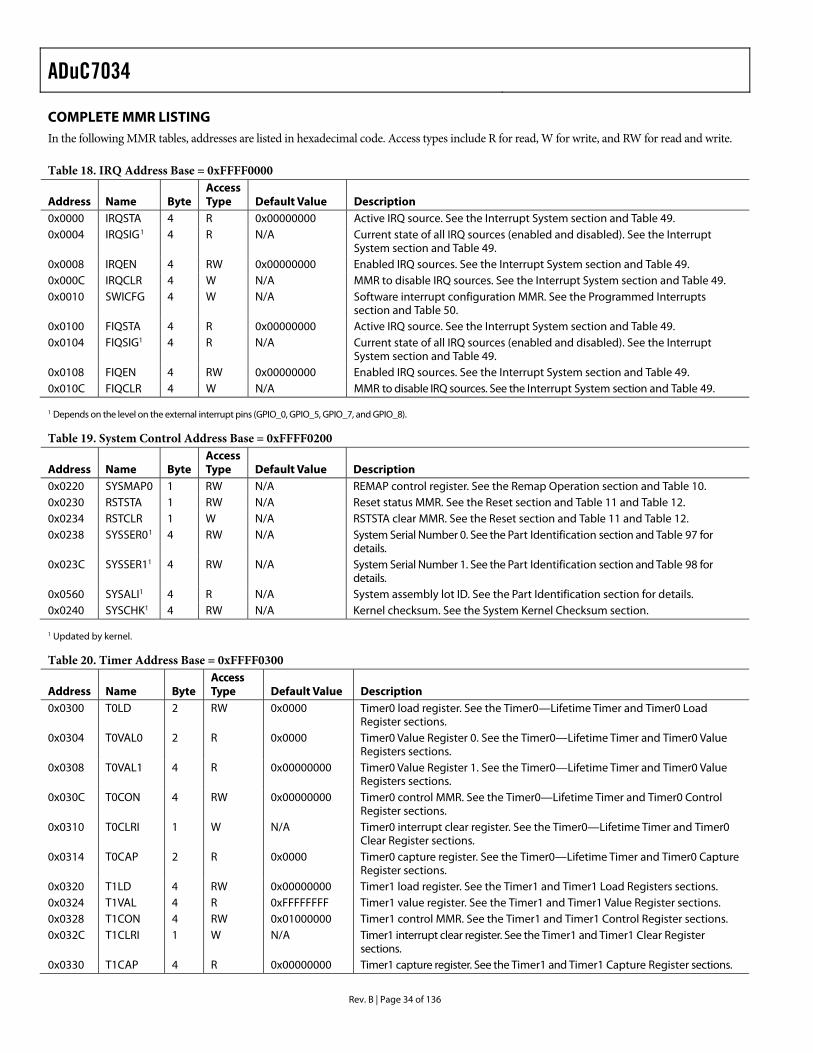
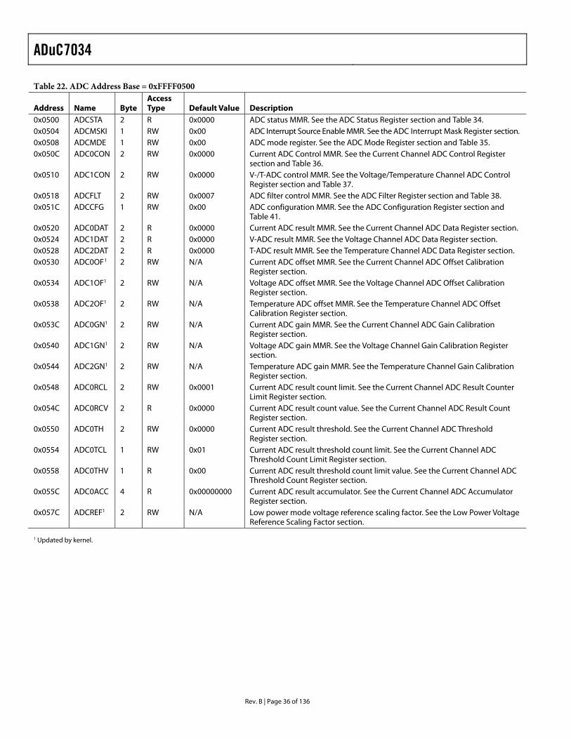
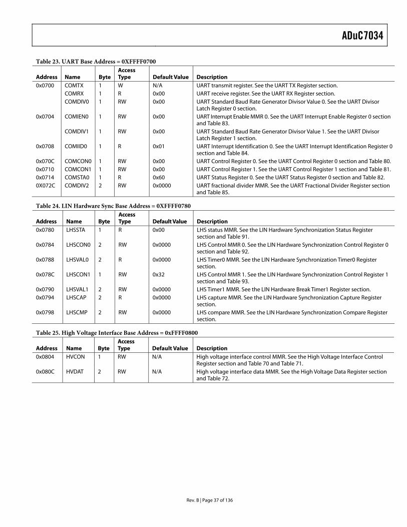
COMPLETE MMR LISTING In the following MMR tables, addresses are listed in hexadecimal code. Access types include R for read, W for write, and RW for read and write.
Table 18. IRQ Address Base = 0xFFFF0000
Address Name Byte Access Type Default Value Description
0x0000 IRQSTA 4 R 0x00000000 Active IRQ source. See the Interrupt System section and Table 49. 0x0004 IRQSIG1 4 R N/A Current state of all IRQ sources (enabled and disabled). See the Interrupt
System section and Table 49. 0x0008 IRQEN 4 RW 0x00000000 Enabled IRQ sources. See the Interrupt System section and Table 49. 0x000C IRQCLR 4 W N/A MMR to disable IRQ sources. See the Interrupt System section and Table 49. 0x0010 SWICFG 4 W N/A Software interrupt configuration MMR. See the Programmed Interrupts
section and Table 50. 0x0100 FIQSTA 4 R 0x00000000 Active IRQ source. See the Interrupt System section and Table 49. 0x0104 FIQSIG1 4 R N/A Current state of all IRQ sources (enabled and disabled). See the Interrupt
System section and Table 49. 0x0108 FIQEN 4 RW 0x00000000 Enabled IRQ sources. See the Interrupt System section and Table 49. 0x010C FIQCLR 4 W N/A MMR to disable IRQ sources. See the Interrupt System section and Table 49. 1 Depends on the level on the external interrupt pins (GPIO_0, GPIO_5, GPIO_7, and GPIO_8).
Table 19. System Control Address Base = 0xFFFF0200
Address Name Byte Access Type Default Value Description
0x0220 SYSMAP0 1 RW N/A REMAP control register. See the Remap Operation section and Table 10. 0x0230 RSTSTA 1 RW N/A Reset status MMR. See the Reset section and Table 11 and Table 12. 0x0234 RSTCLR 1 W N/A RSTSTA clear MMR. See the Reset section and Table 11 and Table 12. 0x0238 SYSSER01 4 RW N/A System Serial Number 0. See the Part Identification section and Table 97 for
details. 0x023C SYSSER11 4 RW N/A System Serial Number 1. See the Part Identification section and Table 98 for
details. 0x0560 SYSALI1 4 R N/A System assembly lot ID. See the Part Identification section for details. 0x0240 SYSCHK1 4 RW N/A Kernel checksum. See the System Kernel Checksum section. 1 Updated by kernel.
Table 20. Timer Address Base = 0xFFFF0300
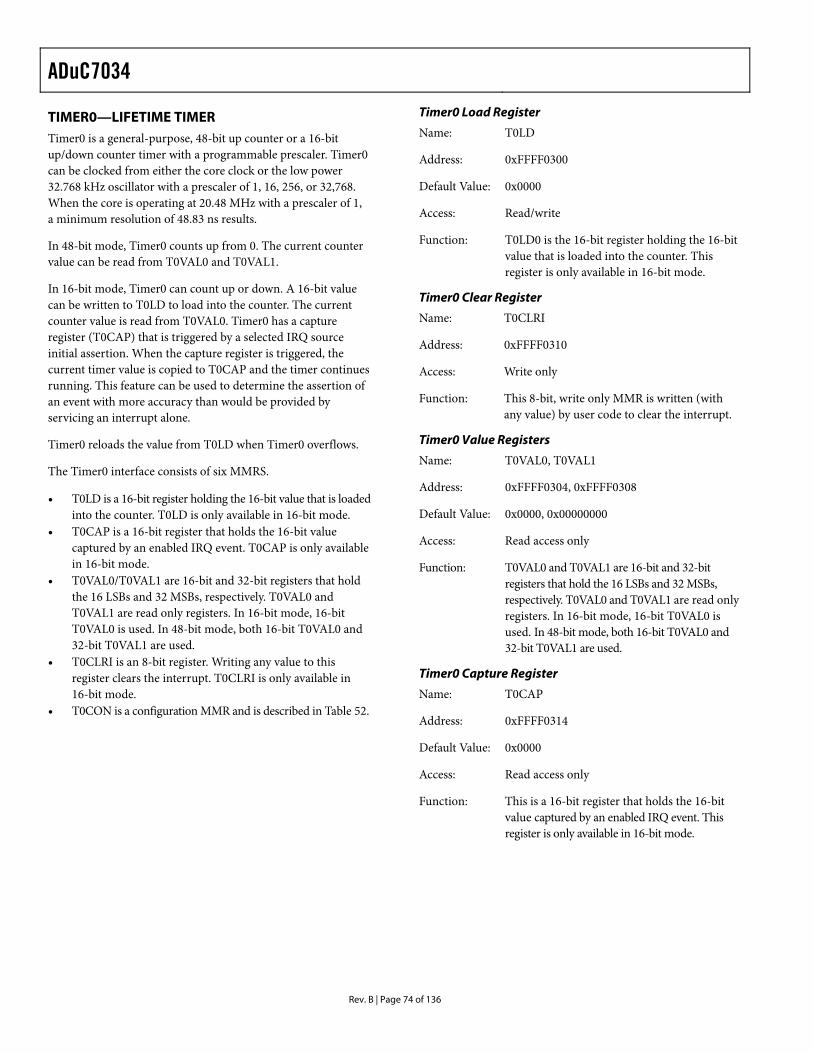
Address Name Byte Access Type Default Value Description
0x0300 T0LD 2 RW 0x0000 Timer0 load register. See the Timer0—Lifetime Timer and Timer0 Load Register sections.
0x0304 T0VAL0 2 R 0x0000 Timer0 Value Register 0. See the Timer0—Lifetime Timer and Timer0 Value Registers sections.
0x0308 T0VAL1 4 R 0x00000000 Timer0 Value Register 1. See the Timer0—Lifetime Timer and Timer0 Value Registers sections.
0x030C T0CON 4 RW 0x00000000 Timer0 control MMR. See the Timer0—Lifetime Timer and Timer0 Control Register sections.
0x0310 T0CLRI 1 W N/A Timer0 interrupt clear register. See the Timer0—Lifetime Timer and Timer0 Clear Register sections.
0x0314 T0CAP 2 R 0x0000 Timer0 capture register. See the Timer0—Lifetime Timer and Timer0 Capture Register sections.
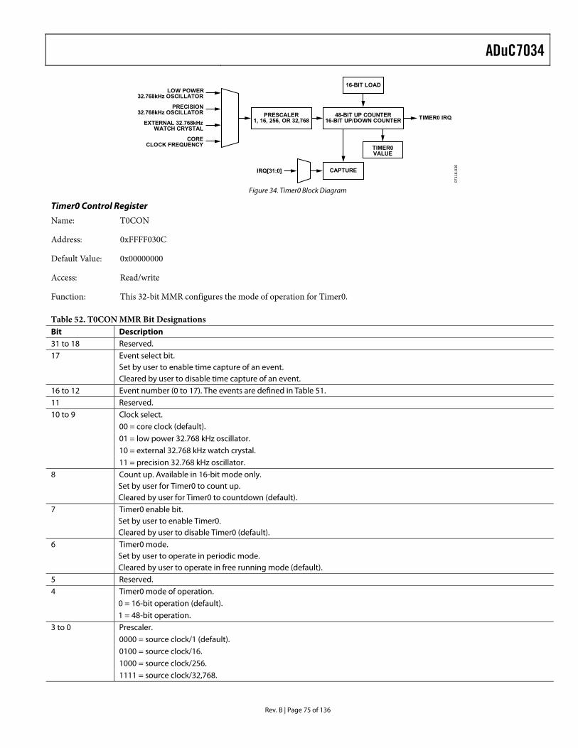
0x0320 T1LD 4 RW 0x00000000 Timer1 load register. See the Timer1 and Timer1 Load Registers sections. 0x0324 T1VAL 4 R 0xFFFFFFFF Timer1 value register. See the Timer1 and Timer1 Value Register sections. 0x0328 T1CON 4 RW 0x01000000 Timer1 control MMR. See the Timer1 and Timer1 Control Register sections. 0x032C T1CLRI 1 W N/A Timer1 interrupt clear register. See the Timer1 and Timer1 Clear Register
sections. 0x0330 T1CAP 4 R 0x00000000 Timer1 capture register. See the Timer1 and Timer1 Capture Register sections.
ADuC7034
Rev. B | Page 35 of 136
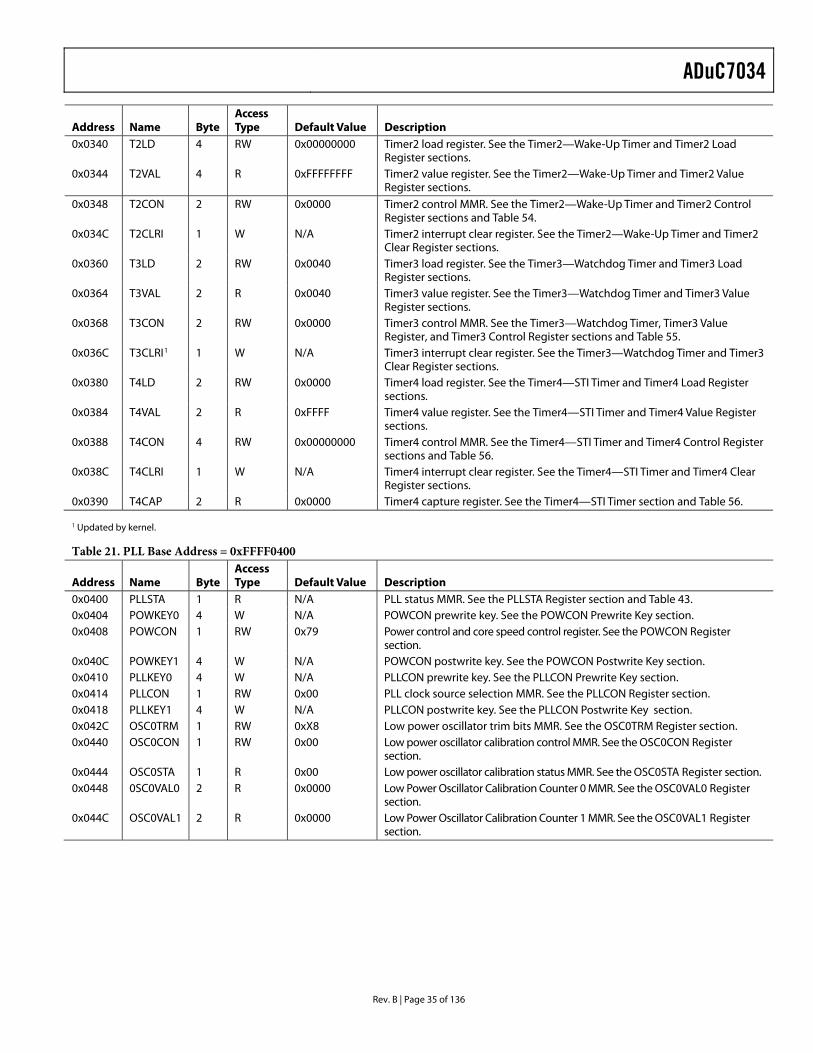
Address Name Byte Access Type Default Value Description
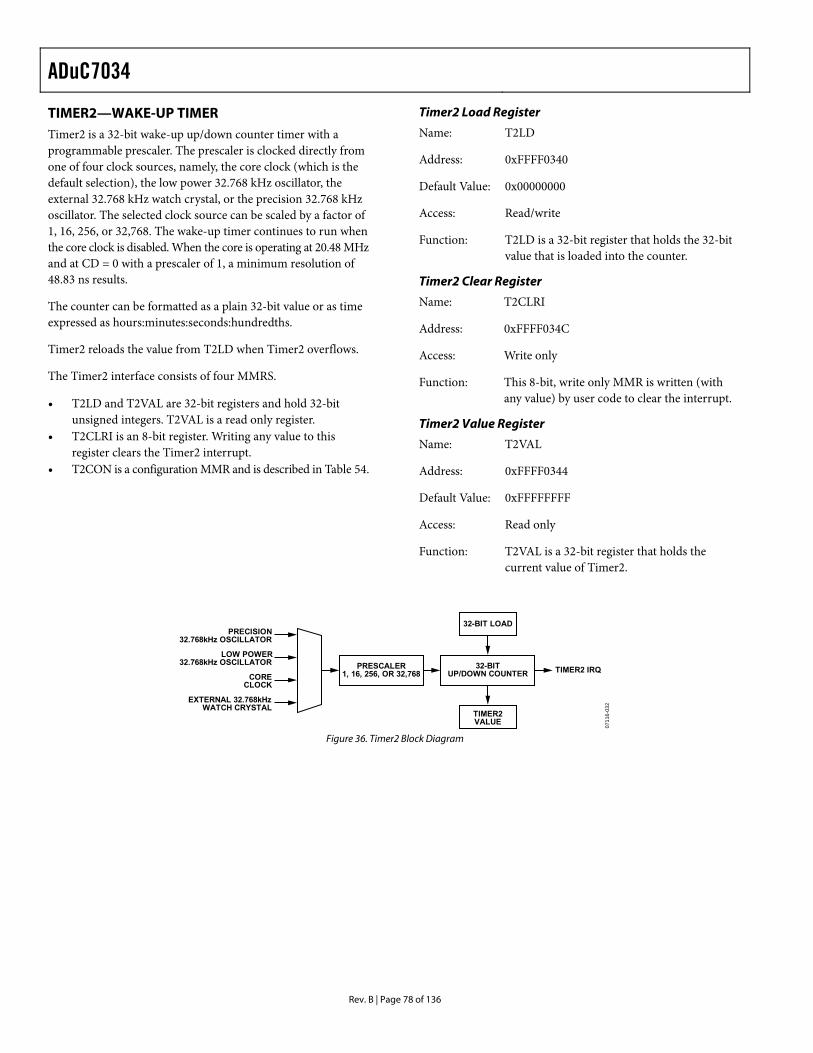
0x0340 T2LD 4 RW 0x00000000 Timer2 load register. See the Timer2—Wake-Up Timer and Timer2 Load Register sections.
0x0344 T2VAL 4 R 0xFFFFFFFF Timer2 value register. See the Timer2—Wake-Up Timer and Timer2 Value Register sections.
0x0348 T2CON 2 RW 0x0000 Timer2 control MMR. See the Timer2—Wake-Up Timer and Timer2 Control Register sections and Table 54.
0x034C T2CLRI 1 W N/A Timer2 interrupt clear register. See the Timer2—Wake-Up Timer and Timer2 Clear Register sections.
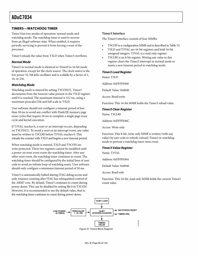
0x0360 T3LD 2 RW 0x0040 Timer3 load register. See the Timer3—Watchdog Timer and Timer3 Load Register sections.
0x0364 T3VAL 2 R 0x0040 Timer3 value register. See the Timer3—Watchdog Timer and Timer3 Value Register sections.
0x0368 T3CON 2 RW 0x0000 Timer3 control MMR. See the Timer3—Watchdog Timer, Timer3 Value Register, and Timer3 Control Register sections and Table 55.
0x036C T3CLRI1 1 W N/A Timer3 interrupt clear register. See the Timer3—Watchdog Timer and Timer3 Clear Register sections.
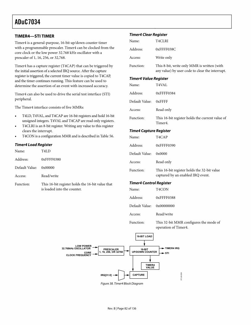
0x0380 T4LD 2 RW 0x0000 Timer4 load register. See the Timer4—STI Timer and Timer4 Load Register sections.
0x0384 T4VAL 2 R 0xFFFF Timer4 value register. See the Timer4—STI Timer and Timer4 Value Register sections.
0x0388 T4CON 4 RW 0x00000000 Timer4 control MMR. See the Timer4—STI Timer and Timer4 Control Register sections and Table 56.
0x038C T4CLRI 1 W N/A Timer4 interrupt clear register. See the Timer4—STI Timer and Timer4 Clear Register sections.
0x0390 T4CAP 2 R 0x0000 Timer4 capture register. See the Timer4—STI Timer section and Table 56. 1 Updated by kernel.
Table 21. PLL Base Address = 0xFFFF0400
Address Name Byte Access Type Default Value Description
0x0400 PLLSTA 1 R N/A PLL status MMR. See the PLLSTA Register section and Table 43. 0x0404 POWKEY0 4 W N/A POWCON prewrite key. See the POWCON Prewrite Key section. 0x0408 POWCON 1 RW 0x79 Power control and core speed control register. See the POWCON Register
section. 0x040C POWKEY1 4 W N/A POWCON postwrite key. See the POWCON Postwrite Key section. 0x0410 PLLKEY0 4 W N/A PLLCON prewrite key. See the PLLCON Prewrite Key section. 0x0414 PLLCON 1 RW 0x00 PLL clock source selection MMR. See the PLLCON Register section. 0x0418 PLLKEY1 4 W N/A PLLCON postwrite key. See the PLLCON Postwrite Key section. 0x042C OSC0TRM 1 RW 0xX8 Low power oscillator trim bits MMR. See the OSC0TRM Register section. 0x0440 OSC0CON 1 RW 0x00 Low power oscillator calibration control MMR. See the OSC0CON Register
section. 0x0444 OSC0STA 1 R 0x00 Low power oscillator calibration status MMR. See the OSC0STA Register section. 0x0448 0SC0VAL0 2 R 0x0000 Low Power Oscillator Calibration Counter 0 MMR. See the OSC0VAL0 Register
section. 0x044C OSC0VAL1 2 R 0x0000 Low Power Oscillator Calibration Counter 1 MMR. See the OSC0VAL1 Register
section.
ADuC7034
Rev. B | Page 36 of 136
Table 22. ADC Address Base = 0xFFFF0500
Address Name Byte Access Type Default Value Description
0x0500 ADCSTA 2 R 0x0000 ADC status MMR. See the ADC Status Register section and Table 34. 0x0504 ADCMSKI 1 RW 0x00 ADC Interrupt Source Enable MMR. See the ADC Interrupt Mask Register section. 0x0508 ADCMDE 1 RW 0x00 ADC mode register. See the ADC Mode Register section and Table 35. 0x050C ADC0CON 2 RW 0x0000 Current ADC Control MMR. See the Current Channel ADC Control Register
section and Table 36. 0x0510 ADC1CON 2 RW 0x0000 V-/T-ADC control MMR. See the Voltage/Temperature Channel ADC Control
Register section and Table 37. 0x0518 ADCFLT 2 RW 0x0007 ADC filter control MMR. See the ADC Filter Register section and Table 38. 0x051C ADCCFG 1 RW 0x00 ADC configuration MMR. See the ADC Configuration Register section and
Table 41. 0x0520 ADC0DAT 2 R 0x0000 Current ADC result MMR. See the Current Channel ADC Data Register section. 0x0524 ADC1DAT 2 R 0x0000 V-ADC result MMR. See the Voltage Channel ADC Data Register section. 0x0528 ADC2DAT 2 R 0x0000 T-ADC result MMR. See the Temperature Channel ADC Data Register section. 0x0530 ADC0OF1 2 RW N/A Current ADC offset MMR. See the Current Channel ADC Offset Calibration
Register section. 0x0534 ADC1OF1 2 RW N/A Voltage ADC offset MMR. See the Voltage Channel ADC Offset Calibration
Register section. 0x0538 ADC2OF1 2 RW N/A Temperature ADC offset MMR. See the Temperature Channel ADC Offset
Calibration Register section. 0x053C ADC0GN1 2 RW N/A Current ADC gain MMR. See the Current Channel ADC Gain Calibration
Register section. 0x0540 ADC1GN1 2 RW N/A Voltage ADC gain MMR. See the Voltage Channel Gain Calibration Register
section. 0x0544 ADC2GN1 2 RW N/A Temperature ADC gain MMR. See the Temperature Channel Gain Calibration
Register section. 0x0548 ADC0RCL 2 RW 0x0001 Current ADC result count limit. See the Current Channel ADC Result Counter
Limit Register section. 0x054C ADC0RCV 2 R 0x0000 Current ADC result count value. See the Current Channel ADC Result Count
Register section. 0x0550 ADC0TH 2 RW 0x0000 Current ADC result threshold. See the Current Channel ADC Threshold
Register section. 0x0554 ADC0TCL 1 RW 0x01 Current ADC result threshold count limit. See the Current Channel ADC
Threshold Count Limit Register section. 0x0558 ADC0THV 1 R 0x00 Current ADC result threshold count limit value. See the Current Channel ADC
Threshold Count Register section. 0x055C ADC0ACC 4 R 0x00000000 Current ADC result accumulator. See the Current Channel ADC Accumulator
Register section. 0x057C ADCREF1 2 RW N/A Low power mode voltage reference scaling factor. See the Low Power Voltage
Reference Scaling Factor section. 1 Updated by kernel.
ADuC7034
Rev. B | Page 37 of 136
Table 23. UART Base Address = 0XFFFF0700
Address Name Byte Access Type Default Value Description
0x0700 COMTX 1 W N/A UART transmit register. See the UART TX Register section. COMRX 1 R 0x00 UART receive register. See the UART RX Register section. COMDIV0 1 RW 0x00 UART Standard Baud Rate Generator Divisor Value 0. See the UART Divisor
and Table 83. COMDIV1 1 RW 0x00 UART Standard Baud Rate Generator Divisor Value 1. See the UART Divisor
Latch Register 1 section. 0x0708 COMIID0 1 R 0x01 UART Interrupt Identification 0. See the UART Interrupt Identification Register 0
section and Table 84. 0x070C COMCON0 1 RW 0x00 UART Control Register 0. See the UART Control Register 0 section and Table 80. 0x0710 COMCON1 1 RW 0x00 UART Control Register 1. See the UART Control Register 1 section and Table 81. 0x0714 COMSTA0 1 R 0x60 UART Status Register 0. See the UART Status Register 0 section and Table 82. 0X072C COMDIV2 2 RW 0x0000 UART fractional divider MMR. See the UART Fractional Divider Register section
and Table 85.
Table 24. LIN Hardware Sync Base Address = 0XFFFF0780
Address Name Byte Access Type Default Value Description
0x0780 LHSSTA 1 R 0x00 LHS status MMR. See the LIN Hardware Synchronization Status Register section and Table 91.
0x0784 LHSCON0 2 RW 0x0000 LHS Control MMR 0. See the LIN Hardware Synchronization Control Register 0 section and Table 92.
0x0788 LHSVAL0 2 R 0x0000 LHS Timer0 MMR. See the LIN Hardware Synchronization Timer0 Register section.
0x078C LHSCON1 1 RW 0x32 LHS Control MMR 1. See the LIN Hardware Synchronization Control Register 1 section and Table 93.
0x0790 LHSVAL1 2 RW 0x0000 LHS Timer1 MMR. See the LIN Hardware Break Timer1 Register section. 0x0794 LHSCAP 2 R 0x0000 LHS capture MMR. See the LIN Hardware Synchronization Capture Register
section. 0x0798 LHSCMP 2 RW 0x0000 LHS compare MMR. See the LIN Hardware Synchronization Compare Register
section.
Table 25. High Voltage Interface Base Address = 0xFFFF0800
Address Name Byte Access Type Default Value Description
0x0804 HVCON 1 RW N/A High voltage interface control MMR. See the High Voltage Interface Control Register section and Table 70 and Table 71.
0x080C HVDAT 2 RW N/A High voltage interface data MMR. See the High Voltage Data Register section and Table 72.
ADuC7034
Rev. B | Page 38 of 136
Table 26. STI Base Address = 0xFFFF0880
Address Name Byte Access Type Default Value Description
0x0880 STIKEY0 4 W N/A STICON prewrite key. See the Serial Test Interface Key0 Register section. 0x0884 STICON 2 RW 0x0000 Serial test interface control MMR. See the Serial Test Interface Control Register
section and Table 90. 0x0888 STIKEY1 4 W N/A STICON postwrite key. See the Serial Test Interface Key1 Register section and
Table 90. 0x088C STIDAT0 2 RW 0x0000 STI Data MMR 0. See the Serial Test Interface Data0 Register section. 0x0890 STIDAT1 2 RW 0x0000 STI Data MMR 1. See the Serial Test Interface Data1 Register section. 0x0894 STIDAT2 2 RW 0x0000 STI Data MMR 2. See the Serial Test Interface Data2 Register section.
Table 27. SPI Base Address = 0xFFFF0A00 Address Name Byte Access Type Default Value Description 0x0A00 SPISTA 1 R 0x00 SPI status MMR. See the SPI Status Register section and Table 89. 0x0A04 SPIRX 1 R 0x00 SPI receive MMR. See the SPI Receive Register section. 0x0A08 SPITX 1 W SPI transmit MMR. See the SPI Transmit Register section. 0x0A0C SPIDIV 1 RW 0x1B SPI baud rate select MMR. See the SPI Divider Register section. 0x0A10 SPICON 2 RW 0x00 SPI control MMR. See the SPI Control Register section and Table 88.
Table 28. GPIO Base Address = 0xFFFF0D00
Address Name Byte Access Type Default Value Description
0x0D00 GP0CON 4 RW 0x11100000 GPIO Port0 control MMR. See the GPIO Port0 Control Register section and Table 58.
0x0D04 GP1CON 4 RW 0x10000000 GPIO Port1 control MMR. See the GPIO Port1 Control Register section and Table 59.
0x0D08 GP2CON 4 RW 0x01000000 GPIO Port2 control MMR. See the GPIO Port2 Control Register section and Table 60.
0x0D20 GP0DAT1 4 RW 0x000000XX GPIO Port0 data control MMR. See the GPIO Port0 Data Register section and Table 61.
0x0D24 GP0SET 4 W GPIO Port0 data set MMR. See the GPIO Port0 Set Register section and Table 64.
0x0D28 GP0CLR 4 W GPIO Port0 data clear MMR. See the GPIO Port0 Clear Register section and Table 67.
0x0D30 GP1DAT1 4 RW 0x000000XX GPIO Port1 data control MMR. See the GPIO Port1 Data Register section and Table 62.
0x0D34 GP1SET 4 W GPIO Port1 data set MMR. See the GPIO Port1 Set Register section and Table 65.
0x0D38 GP1CLR 4 W GPIO Port1 data clear MMR. See the GPIO Port1 Clear Register section and Table 68.
0x0D40 GP2DAT1 4 RW 0x000000XX GPIO Port2 Data Control MMR. See the GPIO Port2 Data Register section and Table 63.
0x0D44 GP2SET 4 W GPIO Port2 data set MMR. See the GPIO Port2 Set Register section and Table 66.
0x0D48 GP2CLR 4 W GPIO Port2 data clear MMR. See the GPIO Port2 Clear Register section and Table 69.
1 Depends on the level on the external GPIO pins.
ADuC7034
Rev. B | Page 39 of 136
Table 29. Flash/EE Base Address = 0xFFFF0E00
Address Name Byte Access Type Default Value Description
0x0E00 FEE0STA 1 R 0x20 Flash/EE status MMR and Table 14. 0x0E04 FEE0MOD 1 RW 0x00 Flash/EE control MMR and Table 15. 0x0E08 FEE0CON 1 RW 0x07 Flash/EE control MMR. See Table 13. 0x0E0C FEE0DAT 2 RW 0x0000 Flash/EE data MMR. 0x0E10 FEE0ADR 2 RW Flash/EE address MMR. 0x0E18 FEE0SIG 3 R 0xFFFFFF Flash/EE LFSR MMR. 0x0E1C FEE0PRO 4 RW 0x00000000 Flash/EE protection MMR. See the Flash/EE Memory Protection Registers
section and Table 16. 0x0E20 FEE0HID 4 RW 0xFFFFFFFF Flash/EE protection MMR. See the Flash/EE Memory Protection Registers and
Table 16.
ADuC7034
Rev. B | Page 40 of 136
16-BIT SIGMA-DELTA ANALOG-TO-DIGITAL CONVERTERS The ADuC7034 incorporates two independent sigma-delta (Σ-Δ) analog-to-digital converters (ADCs), namely, the current channel ADC (I-ADC) and the voltage/temperature channel ADC (V-/T-ADC). These precision measurement channels integrate on-chip buffering, a programmable gain amplifier, 16-bit Σ-Δ modulators, and digital filtering for precise measurement of current, voltage, and temperature variables in 12 V automotive battery systems.
CURRENT CHANNEL ADC (I-ADC) The I-ADC converts battery current sensed through an external 100 μΩ shunt resistor. On-chip programmable gain means that the I-ADC can be configured to accommodate battery current levels from ±1 A to ±1500 A.
As shown in Figure 17, the I-ADC employs a Σ-Δ conversion technique to attain 16 bits of no missing codes performance.
The Σ-Δ modulator converts the sampled input signal into a digital pulse train whose duty cycle contains the digital infor-mation. A modified sinc3 programmable low-pass filter is then employed to decimate the modulator output data stream to provide a valid 16-bit data conversion result at programmable output rates from 4 Hz to 8 kHz in normal mode and from 1 Hz to 2 kHz in low power mode.
The I-ADC also incorporates counter, comparator, and accumulator logic. This allows the I-ADC result to generate an interrupt after a predefined number of conversions has elapsed or a programmable threshold value has been exceeded. A fast ADC overrange feature is also supported. Once enabled, a 32-bit accumulator automatically sums the 16-bit I-ADC results.
The time to a first valid (fully settled) result on the current channel is three ADC conversion cycles with chop mode disabled and two ADC conversion cycles with chop mode enabled.
ADuC7034
Rev. B | Page 41 of 136
PGA
AD
CTH
RES
HO
LD
AD
CR
ESU
LT
OU
TPU
TFO
RM
AT
BU
F
CH
OP
CH
OP
AN
ALO
G IN
PUT
DIA
GN
OST
ICC
UR
REN
T SO
UR
CES
TWO
50µ
A II
N+
AN
D II
N–
CU
RR
ENT
SOU
RC
ES.
AN
ALO
G IN
PUT
DIA
GN
OST
ICVO
LTA
GE
SOU
RC
E
VREF
/136
VO
LTA
GE
INPU
T.
AN
ALO
G IN
PUT
PRO
GR
AM
MA
BLE
CH
OPP
ING
THE
INPU
TS A
RE
ALT
ERN
ATE
LY R
EVER
SED
THR
OU
GH
TH
EC
ON
VER
SIO
N C
YCLE
.
Σ-Δ
AD
C
THE Σ-Δ
AR
CH
ITEC
TUR
EEN
SUR
ES 1
6 B
ITS
NO
MIS
SIN
G C
OD
ES.
OU
TPU
T A
VER
AG
E
AS
PAR
T O
F TH
E C
HO
PPIN
GIM
PLEM
ENTA
TIO
N, E
AC
HD
ATA
-WO
RD
OU
TPU
T FR
OM
THE
FILT
ER IS
SU
MM
ED A
ND
AVE
RA
GED
WIT
H IT
SPR
EDEC
ESSO
R.
AD
C F
AST
OVE
RR
AN
GE
GEN
ERA
TES
AN
AD
CIN
TER
RU
PT IF
TH
E C
UR
REN
TIN
PUT
IS G
RO
SSLY
OVE
RR
AN
GED
.A
DC
AC
CU
MU
LATO
R
AC
CU
MU
LATE
S TH
EA
DC
RES
ULT
.
PRO
GR
AM
MA
BLE
GA
INA
MPL
IFIE
R
THE
PRO
GR
AM
MA
BLE
GA
IN A
MPL
IFIE
R A
LLO
WS
EIG
HT
BIP
OLA
R IN
PUT
RA
NG
ES F
RO
M ±
2.3m
V TO
±1.2
V (IN
T VR
EF =
+1.
2V).
Σ-Δ
MO
DU
LATO
R
THE
MO
DU
LATO
R P
RO
VID
ES A
HIG
H F
REQ
UEN
CY,
1-B
IT D
ATA
STR
EAM
(TH
E O
UTP
UT
OF
WH
ICH
IS A
LSO
CH
OPP
ED) T
OTH
E D
IGIT
AL
FILT
ER, T
HE
DU
TYC
YCLE
OF
WH
ICH
REP
RES
ENTS
THE
SAM
PLED
AN
ALO
G IN
PUT
VOLT
AG
E.
IIN+
IIN–
VREF
/136
GN
DREG
_AVD
DR
EG_A
VDD
Σ-Δ
AD
C
Σ-Δ
MO
DU
LATO
RPR
OG
RA
MM
AB
LED
IGIT
AL
FILT
ER
OU
TPU
TA
VER
AG
E
OFF
SET
CO
EFFI
CIE
NT
GA
INC
OEF
FIC
IEN
T
AD
CIN
TER
RU
PT
AD
C R
ESU
LTA
CC
UM
ULA
TOR
AD
CR
ESU
LT
AD
C R
ESU
LTC
OU
NTE
R
THR
ESH
OLD
CO
UN
TER
AD
C IN
TER
RU
PTG
ENER
ATO
R
GEN
ERA
TES
AN
AD
CR
ESU
LT F
RO
M A
NY
ON
E O
F FO
UR
SOU
RC
ES.
AD
C R
ESU
LT C
OU
NTE
R
CO
UN
TS A
DC
RES
ULT
S,G
ENER
ATE
S A
N IN
TER
RU
PTO
N C
OU
NTE
R O
VER
FLO
W.
THR
ESH
OLD
CO
UN
TER
CO
UN
TS U
P IF
AD
CR
ESU
LTS
> TH
RES
HO
LD;
CO
UN
TS D
OW
N/R
ESET
IFA
DC
RES
ULT
< T
HR
ESH
OLD
.G
ENER
ATE
S A
N IN
TER
RU
PTO
N C
OU
NTE
R O
VER
FLO
W.
BU
FFER
AM
PLIF
IER
THE
BU
FFER
AM
PLIF
IER
PR
ESEN
TSA
HIG
H IM
PED
AN
CE
INPU
T ST
AG
E FO
RTH
E PG
A D
RIV
ING
TH
EΣ-Δ
MO
DU
LATO
R.
PREC
ISIO
N R
EFER
ENC
E
THE
INTE
RN
AL
5ppm
/°C
REF
EREN
CE
IS R
OU
TED
TO
THE
AD
C B
Y D
EFA
ULT
. AN
EXTE
RN
AL
REF
EREN
CE
ON
THE
VREF
PIN
CA
N A
LSO
BE
SELE
CTE
D.
INTE
RN
AL
REF
EREN
CE
VREF
PRO
GR
AM
MA
BLE
DIG
ITA
L FI
LTER
THE
SIN
C3
FILT
ER R
EMO
VES
QU
AN
TIZA
TIO
N N
OIS
E IN
TRO
DU
CED
BY
THE
MO
DU
LATO
R. T
HE
UPD
ATE
RA
TE A
ND
BA
ND
WID
TH O
F TH
ISFI
LTER
AR
E PR
OG
RA
MM
AB
LE V
IATH
E A
DC
FLT
MM
R.
DIG
ITA
L C
OM
PAR
ATO
R
THE
AD
C R
ESU
LT IS
CO
MPA
RED
TO
APR
ESET
TH
RES
HO
LD.
OU
TPU
T SC
ALI
NG
THE
OU
TPU
T W
OR
D F
RO
MTH
E D
IGIT
AL
FILT
ER IS
SCA
LED
BY
THE
CA
LIB
RA
TIO
NC
OEF
FIC
IEN
TS B
EFO
RE
BEI
NG
PRO
VID
ED A
S TH
EC
ON
VER
SIO
N R
ESU
LT.
07116-015
Figure 17. Current ADC, Top-Level Overview
ADuC7034
Rev. B | Page 42 of 136
VOLTAGE/TEMPERATURE CHANNEL ADC (V-/T-ADC) The voltage/temperature channel ADC (V-/T-ADC) converts additional battery parameters, such as voltage and temperature. The input to this channel can be multiplexed from one of three input sources, namely, an external voltage, an external tempera-ture sensor circuit, or an on-chip temperature sensor.
As with the current channel ADC (I-ADC), the V-/T-ADC employs an identical Σ-Δ conversion technique, including a modified sinc3 low-pass filter to provide a valid 16-bit data conversion result at programmable output rates from 4 Hz to 8 kHz. An external RC filter network is not required because it is internally implemented in the voltage channel.
The external battery voltage (VBAT) is routed to the ADC input via an on-chip high voltage (divide-by-24) resistive attenuator. The voltage attenuator buffers are automatically enabled when the voltage attenuator input is selected.
The battery temperature can be derived through the on-chip temperature sensor or an external temperature sensor input. The time to a first valid (fully settled) result after an input channel switch on the voltage/temperature channel is three ADC conversion cycles with chop mode disabled.
This ADC is again buffered but, unlike the current channel, has a fixed input range of 0 V to VREF on VTEMP and 0 V to 28.8 V on VBAT (assuming an internal 1.2 V reference). A top-level overview of this ADC signal chain is shown in Figure 18.
ADCRESULT
OUTPUTFORMAT
CHOP
Σ-Δ ADC
THE Σ-ΔARCHITECTURE
ENSURES 16 BITSNO MISSING CODES.
OUTPUT AVERAGE
AS PART OF THE CHOPPINGIMPLEMENTATION, EACH
DATA-WORD OUTPUT FROMTHE FILTER IS SUMMED AND
AVERAGED WITH ITSPREDECESSOR.
Σ-Δ MODULATOR
THE MODULATOR PROVIDES AHIGH FREQUENCY, 1-BIT DATA
STREAM (THE OUTPUT OFWHICH IS ALSO CHOPPED) TO
THE DIGITAL FILTER, THE DUTYCYCLE OF WHICH REPRESENTSTHE SAMPLED ANALOG INPUT
VOLTAGE.
Σ-Δ ADC
Σ-ΔMODULATOR
PROGRAMMABLEDIGITAL FILTER
OUTPUTAVERAGE
OFFSETCOEFFICIENT
GAINCOEFFICIENT
ADC INTERRUPT GENERATOR
GENERATES AN ADCINTERRUPT AFTER A VOLTAGE
OR TEMPERATURECONVERSION IS COMPLETED.
PRECISION REFERENCE
THE INTERNAL 5ppm/°CREFERENCE IS ROUTED TOTHE ADC BY DEFAULT. ANEXTERNAL REFERENCE ON
THE VREF PIN CAN ALSOBE SELECTED.
BUF
INTERNALTEMP
BUF
CHOPMUX
INTERNALREFERENCE
VREF
PROGRAMMABLEDIGITAL FILTER
THE SINC3 FILTER REMOVESQUANTIZATION NOISE INTRODUCEDBY THE MODULATOR. THE UPDATE
RATE AND BANDWIDTH OF THISFILTER ARE PROGRAMMABLE VIA
THE ADCFLT MMR.
OUTPUT SCALING
THE OUTPUT WORD FROMTHE DIGITAL FILTER IS
SCALED BY THE CALIBRATIONCOEFFICIENTS BEFORE BEING
ADC GROUND SWITCH The ADuC7034 features an integrated ground switch pin, GND_SW (Pin 15). This switch allows the user to dynamically disconnect the ground from external devices and instead use either a direct connection to ground or a connection to ground via a 20 kΩ resistor. If the latter option is chosen, the additional resistor can be used to reduce the number of external components required for an NTC circuit. In addition, the ground switch feature can be used to reduce power consumption on application-specific boards.
An example application is shown in Figure 19.
RREF
REG_AVDD
VTEMP
NTC
20kΩ
REG_AVDD
VTEMP
GND_SW GND_SW
NTC
0711
6-01
7
Figure 19. Example External Temperature Sensor Circuits
Figure 19 shows an external NTC used in two modes, with one using the internal 20 kΩ resistor and the second showing a direct connection to ground via the GND_SW.
ADCCFG[7] controls the connection of the ground switch to ground, and ADCMDE[6] controls the GND_SW resistance, as shown in Figure 20.
20kΩ
GND_SW
ADCMDE[6]
ADCCFG[7]
0711
6-01
8
Figure 20. Internal Ground Switch Configuration
The possible combinations of ADCCFG[7] and ADCMDE[6] are shown in Table 30.
Table 30. GND_SW Configuration ADCCFG[7] ADCMDE[6] GND_SW 0 0 Floating 0 1 Floating 1 0 Direct connection to ground 1 1 Connected to ground via 20 kΩ
resistor
ADC NOISE PERFORMANCE TABLES Table 31, Table 32, and Table 33 list the output rms noise in microvolts for some typical output update rates on the I-ADC and V-/T-ADC. The numbers are typical and are generated at a differential input voltage of 0 V. The output rms noise is specified as the standard deviation (or 1 Σ) of the distribution of ADC output codes collected when the ADC input voltage is at a dc voltage. It is expressed in microvolts rms.
Table 31. Typical Output RMS Noise of Current Channel ADC in Normal Power Mode
Table 32. Typical Output RMS Noise (Referred to ADC Voltage Attenuator Input) of Voltage Channel ADC ADCFLT Data Update Rate 28.8 V ADC Input Range 0xBF1D 4 Hz 65 μV 0x961F 10 Hz 65 μV 0x0007 1 kHz 180 μV 0x0000 8 kHz 1600 μV
Table 33. Typical Output RMS Noise of Temperature Channel ADC ADCFLT Data Update Rate 0 V to 1.2 V ADC Input Range 0xBF1D 4 Hz 2.8 μV 0x961F 10 Hz 2.8 μV 0x0007 1 kHz 7.5 μV 0x0000 8 kHz 55 μV
ADuC7034
Rev. B | Page 44 of 136
ADC MMR INTERFACE The ADC is controlled and configured through several MMRs that are described in detail in the ADC Status Register to Low Power Voltage Reference Scaling Factor Registersections.
All bits defined in the top eight MSBs (Bits[15:8]) of the ADCSTA MMR are used as flags only and do not generate interrupts. All bits defined in the lower eight LSBs (Bits[7:0]) of this MMR are logic OR’ed to produce a single ADC interrupt to the MCU core. In response to an ADC interrupt, user code should interrogate the ADCSTA MMR to determine the source of the interrupt. Each ADC interrupt source can be individually masked via the ADCMSKI MMR described in ADC Interrupt Mask Register section.
All ADC result ready bits are cleared by a read of the ADC0DAT MMR. If the current channel ADC is not enabled, all ADC result ready bits are cleared by a read of the ADC1DAT or ADC2DAT MMR. To ensure that I-ADC and V-/T-ADC conversion data are synchronous, user code should first read
the ADC1DAT MMR and then read the ADC0DAT MMR. New ADC conversion results are not written to the ADCxDAT MMRs unless the respective ADC result ready bits are first cleared. The only exception to this rule is that the data conversion result updates when the ARM core is powered down. In this mode, the ADCxDAT registers always contain the most recent ADC conversion result, even if the ready bits have not been cleared.
ADC Status Register
Name: ADCSTA
Address: 0xFFFF0500
Default Value: 0x0000
Access: Read only
Function: This read only register holds general status information related to the mode of operation or current status of the ADuC7034 ADCs.
Table 34. ADCSTA MMR Bit Designations Bit Description 15 ADC calibration status. Set automatically in hardware to indicate that an ADC calibration cycle has been completed. Cleared after ADCMDE is written to. 14 ADC temperature conversion error. Set automatically in hardware to indicate that a temperature conversion overrange or underrange has occurred. The
conversion result is clamped to negative full scale (underrange error) or positive full scale (overrange error) in this case. Cleared when a valid (in-range) temperature conversion result is written to the ADC2DAT register. 13 ADC voltage conversion error. Set automatically in hardware to indicate that a voltage conversion overrange or underrange has occurred. The conversion
result is clamped to negative full scale (underrange error) or positive full scale (overrange error) in this case. Cleared when a valid (in-range) voltage conversion result is written to the ADC1DAT register. 12 ADC current conversion error. Set automatically in hardware to indicate that a current conversion overrange or underrange has occurred. The conversion
result is clamped to negative full scale (underrange error) or positive full scale (overrange error) in this case. Cleared when a valid (in-range) current conversion result is written to the ADC0DAT register. 11 to 5 Not used. These bits are reserved for future functionality and should not be monitored by user code. 4 Current channel ADC comparator threshold. This bit is only valid if the current channel ADC comparator is enabled via
the ADCCFG MMR. Set by hardware if the absolute value of the I-ADC conversion result exceeds the value written in the ADC0TH MMR;
however, if the ADC threshold counter is used (ADC0TCL), this bit is set only when the specified number of I-ADC conversions equals the value in the ADC0THV MMR.
Cleared by a reconfiguration of the ADC or if the comparator threshold is disabled. 3 Current channel ADC overrange bit. This bit is updated every 125 μs. Set by hardware if the I-ADC input is approximately more than 30% overrange and the overrange detect function is
enabled via the ADCCFG MMR. Cleared by software only when ADCCFG[2] is cleared to disable the function or when the ADC gain is changed via the
ADC0CON MMR. 2 Temperature conversion result ready bit. Set by hardware as soon as a valid temperature conversion result is written in the temperature data register (ADC2DAT MMR)
if the temperature channel ADC is enabled. It is also set at the end of a calibration. Cleared by reading either ADC2DAT or ADC0DAT.
ADuC7034
Rev. B | Page 45 of 136
Bit Description 1 Voltage conversion result ready bit. Set by hardware as soon as a valid voltage conversion result is written in the voltage data register (ADC1DAT MMR) if the
voltage channel ADC is enabled. It is also set at the end of a calibration. Cleared by reading either ADC1DAT or ADC0DAT. 0 Current conversion result ready bit. Set by hardware as soon as a valid current conversion result is written in the current data register (ADC0DAT MMR) if the
current channel ADC is enabled. It is also set at the end of a calibration. Cleared by reading ADC0DAT.
ADC Interrupt Mask Register
Name: ADCMSKI
Address: 0xFFFF0504
Default Value: 0x00
Access: Read/write
Function: This register allows the ADC interrupt sources to be individually enabled. The bit positions in this register are the same as the lower eight bits in the ADCSTA MMR. If a bit is set to 1 by user code, the respective interrupt is enabled. By default, all bits are 0, meaning all ADC interrupt sources are disabled.
ADuC7034
Rev. B | Page 46 of 136
ADC Mode Register
Name: ADCMDE
Address: 0xFFFF0508
Default Value: 0x00
Access: Read/write
Function: The ADC mode MMR is an 8-bit register that configures the mode of operation of the ADC subsystem.
Table 35. ADCMDE MMR Bit Designations Bit Description 7 Not used. This bit is reserved for future functionality and should be written as 0 by user code. 6 20 kΩ resistor select. 1 = selects the 20 kΩ resistor shown in Figure 20. 0 = selects the direct path to ground shown in Figure 20 (default). 5 Low power mode reference select. 1 = enables the precision voltage reference in either low power mode or low power plus mode. Enabling the precision
voltage reference in low power modes requires additional current and therefore results in increased current consumption. 0 = enables the low power voltage reference in either low power mode or low power plus mode (default). 4 to 3 ADC power mode configuration. 00 = ADC normal mode. If enabled, the ADC operates with normal current consumption, yielding optimum electrical
performance. 01 = ADC low power mode. If enabled, the I-ADC operates with reduced current consumption. This limitation in current
consumption is achieved, but at the expense of degrading ADC noise performance, by fixing the gain to 128 and using the on-chip low power 131 kHz oscillator to directly drive the ADC circuits.
10 = ADC low power plus mode. If this bit is enabled, the ADC operates with reduced current consumption. In this mode, the gain is fixed to 512 and the current consumed is approximately 200 μA more than the ADC low power mode. The additional current consumed also ensures that the ADC noise performance is better than that achieved in ADC low power mode.
11 = not defined. 2 to 0 ADC operation mode configuration. 000 = ADC power-down mode. All ADC circuits, including the internal reference, are powered down. 001 = ADC continuous conversion mode. In this mode, any enabled ADC continuously converts. 010 = ADC single conversion mode. In this mode, any enabled ADC performs a single conversion. The ADC enters idle
mode when the single conversion is complete. A single conversion takes two to three ADC clock cycles, depending on the chop mode.
011 = ADC idle mode. In this mode, the ADC is fully powered on but is held in reset. 100 = ADC self-offset calibration. In this mode, an offset calibration is performed on any enabled ADC using an internally
generated 0 V. The calibration is carried out at the user programmed ADC settings; therefore, as with a normal single ADC conversion, it takes two to three ADC conversion cycles before a fully settled calibration result is ready. The calibration result is automatically written to the ADCxOF MMR of the respective ADC. The ADC returns to idle mode and the calibration and conversion ready status bits are set at the end of an offset calibration cycle.
101 = ADC self-gain calibration. In this mode, a gain calibration to an internal reference voltage is performed on all enabled ADCs. A gain calibration is a two-stage process and takes twice the time of an offset calibration. The calibration result is automatically written to the ADCxGN MMR of the respective ADC. The ADC returns to idle mode, and the calibration and conversion ready status bits are set at the end of a gain calibration cycle. An ADC self-gain calibration should only be performed on the current channel ADC. Preprogrammed, factory-set calibration coefficients (downloaded automatically from internal Flash/EE) should be used for voltage temperature measurements. If an external NTC is used, an ADC self-calibration should be performed on the temperature channel.
110 = ADC system zero-scale calibration. In this mode, a zero-scale calibration is performed on enabled ADC channels to an external zero-scale voltage driven at the ADC input pins. The calibration is performed at the user programmed ADC settings; therefore, as with a single ADC conversion, three ADC conversion cycles are required before a fully settled calibration result is available.
111 = ADC system full-scale calibration. In this mode, a full-scale calibration is performed on enabled ADC channels to an external full-scale voltage driven at the ADC input pins.
ADuC7034
Rev. B | Page 47 of 136
Current Channel ADC Control Register Name: ADC0CON
Address: 0xFFFF050C
Default Value: 0x0000
Access: Read/write
Function: The current channel ADC control MMR is a 16-bit register that is used to configure the I-ADC.
Note: If the current ADC is reconfigured via ADC0CON, the voltage ADC and temperature ADC are also reset.
Table 36. ADC0CON MMR Bit Designations Bit Description 15 Current channel ADC enable. Set to 1 by user code to enable the I-ADC. Clearing this bit to 0 powers down the I-ADC and resets the respective ADC ready bit in the ADCSTA MMR to 0. 14 to 13 IIN current source enable. 00 = disables current sources. 01 = enables 50 μA current source on IIN+. 10 = enables 50 μA current source on IIN−. 11 = enables 50 μA current source on both IIN− and IIN+. 12 to 10 Not used. These bits are reserved for future functionality and should be written as 0. 9 Current channel ADC output coding. Set to 1 by user code to configure I-ADC output coding as unipolar. Cleared to 0 by user code to configure I-ADC output coding as twos complement. 8 Not used. This bit is reserved for future functionality and should be written as 0. 7 to 6 Current channel ADC inputs select. 00 = IIN+ and IIN− are selected. 01 = IIN− and IIN− are selected. Diagnostic, internal short configuration. 10 = VREF/136 and 0 V are selected. Diagnostic, test voltage for gain settings ≤ 128. If the reference REG_AVDD and
AGND divided by 2 is selected, REG_AVDD is used for VREF. This leads to ADC0DAT being scaled by 2. 11 = not defined. 5 to 4 Current channel ADC reference select. 00 = internal 1.2 V precision reference is selected. In ADC low power mode, the voltage reference selection is controlled
by ADCMDE[5]. 01 = external reference inputs VREF and GND_SW are selected. 10 = external reference inputs divided by 2 (that is, VREF and GND_SW divided by 2) are selected, which allows an
external reference up to REG_AVDD. 11 = the reference REG_AVDD and AGND divided by 2 is selected. 3 to 0 Current channel ADC gain select. The nominal I-ADC full-scale input voltage is VREF/gain. 0000 = I-ADC gain of 1. 0001 = I-ADC gain of 2. 0010 = I-ADC gain of 4. 0011 = I-ADC gain of 8. 0100 = I-ADC gain of 16. 0101 = I-ADC gain of 32. 0110 = I-ADC gain of 64. 0111 = I-ADC gain of 128. 1000 = I-ADC gain of 256. 1001 = I-ADC gain of 512. 1010 = I-ADC gain is undefined. 1011 = I-ADC gain is undefined. 1100 = I-ADC gain is undefined. 1101 = I-ADC gain is undefined. 1110 = I-ADC gain is undefined. 1111 = I-ADC gain is undefined.
ADuC7034
Rev. B | Page 48 of 136
Voltage/Temperature Channel ADC Control Register
Name: ADC1CON
Address: 0xFFFF0510
Default Value: 0x0000
Access: Read/write
Function: The voltage/temperature channel ADC control MMR is a 16-bit register that is used to configure the V-/T-ADC.
Note: If the VBAT attenuator input is selected, the voltage attenuator buffers are automatically enabled.
Table 37. ADC1CON MMR Bit Designations Bit Description 15 Voltage/temperature channel ADC enable. Set to 1 by user code to enable the V-/T-ADC. Clearing this bit to 0 powers down the V-/T-ADC. 14 to 13 VTEMP current source enable. 00 = disables current sources. 01 = enables 50 μA current source on VTEMP. 10 = enables 50 μA current source on GND_SW. 11 = enables 50 μA current source on both VTEMP and GND_SW. 12 to 10 Not used. These bits are reserved for future functionality and should not be modified by user code. 9 Voltage/temperature channel ADC output coding. Set to 1 by user code to configure V-/T-ADC output coding as unipolar. Cleared to 0 by user code to configure V-/T-ADC output coding as twos complement. 8 Not used. This bit is reserved for future functionality and should be written as 0 by user code. 7 to 6 Voltage/temperature channel ADC input select. 00 = VBAT attenuator (VBAT/24 and AGND) is selected. The high voltage buffers are enabled automatically in this
configuration. The conversion result is written to ADC1DAT. 01 = external temperature inputs (VTEMP and GND_SW) are selected. The conversion result is written to ADC2DAT. 10 = internal sensor is selected. Internal temperature sensor input selected, conversion result written to ADC2DAT. The
temperature gradient is 0.33 mV/°C; this is only applicable to the internal temperature sensor. 11 = internal short is selected. Shorted input. The conversion result is written to ADC1DAT. 5 to 4 Voltage/temperature channel ADC reference select. 00 = internal 1.2 V precision reference is selected. 01 = external reference inputs VREF and GND_SW are selected. 10 = external reference inputs divided by 2 (that is, VREF and GND_SW divided by 2) are selected. This allows an external
reference up to REG_AVDD. 11 = the reference input REG_AVDD and AGND divided by 2 are selected for the voltage channel.
The reference inputs REG_AVDD and GND_SW divided by 2 are selected for the temperature channel. 3 to 0 Not used. These bits are reserved for future functionality and should not be written as 0 by user code.
ADuC7034
Rev. B | Page 49 of 136
ADC Filter Register
Name: ADCFLT
Address: 0xFFFF0518
Default Value: 0x0007
Access: Read/write
Function: The ADC filter MMR is a 16-bit register that controls the speed and resolution of the on-chip ADCs.
Note: If ADCFLT is modified, the current and voltage/temperature ADCs are reset.
Table 38. ADCFLT MMR Bit Designations Bit Description 15 Chop enable. Set by the user to enable system chopping of all active ADCs. When this bit is set, the ADC has very low offset errors and
drift, but the ADC output rate is reduced by a factor of 3 if AF = 0 (see the sinc3 decimation factor, Bits[6:0], in this table). If AF > 0, the ADC output update rate is the same with chop enabled or disabled. When chop is enabled, the settling time is two output periods.
Cleared by user code to disable system chopping. 14 Running average. Set by the user to enable a running-average-by-two function, which reduces ADC noise. This function is automatically
enabled when chopping is active and is an optional feature when chopping is inactive. The ADC output rate is not reduced if the running average function is enabled when chopping is inactive; instead, the settling time is increased by one conversion period.
Cleared by the user to disable the running average function. 13 to 8 Averaging factor (AF). The values written to these bits are used to implement a programmable first-order sinc3 postfilter.
The averaging factor can further reduce ADC noise at the expense of output rate, as described in the sinc3 decimation factor, Bits[6:0], in this table.
7 Sinc3 modify. Set by the user to modify the standard sinc3 frequency response and increase the stop-band rejection of the filter by approximately 5 dB. This is achieved by inserting a second notch (NOTCH2) at fNOTCH2 = 1.333 × fNOTCH, where fNOTCH is the location of the first notch in the response.
6 to 0 Sinc3 decimation factor (SF).1 The value written in these bits controls the oversampling (decimation factor) of the sinc3 filter. The output rate from the sinc3 filter is given by fADC = (512,000/([SF + 1] × 64)) Hz2 when the chop enable bit (Bit 15) = 0 and the averaging factor (AF) = 0. This is valid for all SF values ≤ 125.
For SF = 126, fADC is forced to 60 Hz. For SF = 127, fADC is forced to 50 Hz. For information on calculating the fADC for SF (other than 126 and 127) and AF values, refer to Table 39.
1 Due to limitations on the digital filter internal data path, there are some limitations on the combinations of the sinc3 decimation factor (SF) and the averaging factor (AF)
that can be used to generate a required ADC output rate. This restriction limits the minimum ADC update in normal power mode to 4 Hz or 1 Hz in lower power mode. 2 In low power mode or low power plus mode, the ADC is driven directly by the low power 131 kHz oscillator, not by 512 kHz. All fADC calculations should be divided by 4
(approximately).
ADuC7034
Rev. B | Page 50 of 136
Table 39. ADC Conversion Rates and Settling Times Chop Enabled Averaging Factor
Running Average fADC tSETTLING
1 Disabled Disabled Disabled
64]1[ ×+SF
000,512
3
ADCf
Disabled Disabled Enabled
64]1[ ×+SF
000,512
4
ADCf
Disabled Enabled Disabled
]3[64]1[ AFSF +××+000,512
1
ADCf
Disabled Enabled Enabled
]3[64]1[ AFSF +××+000,512
ADCf
2
Enabled N/A N/A
3]3[64]1[000,512
++××+ AFSF
ADCf2
1 An additional time of approximately 60 μs per ADC is required before the first ADC is available.
Table 40. Allowable Combinations of SF and AF AF Value SF Value 0 1 to 7 8 to 63 0 to 31 Yes Yes Yes 32 to 63 Yes Yes No 64 to 127 Yes No No
ADuC7034
Rev. B | Page 51 of 136
ADC Configuration Register
Name: ADCCFG
Address: 0xFFFF051C
Default Value: 0x00
Access: Read/write
Function: The 8-bit ADC configuration MMR controls extended functionality related to the on-chip ADCs.
Table 41. ADCCFG MMR Bit Designations Bit Description 7 Analog ground switch enable. Set to 1 by user software to connect the external GND_SW pin (Pin 15) to an internal analog ground reference point.
This bit can be used to connect and disconnect external circuits and components to ground under program control and thereby minimize dc current consumption when the external circuit or component is not being used. This bit is used in conjunction with ADCMDE[6] to select a 20 kΩ resistor to ground.
Cleared by user code to disconnect the external GND_SW pin. 6 to 5 Current channel (32-bit) accumulator enable. 00 = accumulator disabled and reset to 0. The accumulator must be disabled for a full ADC conversion (ADCSTA[0] set
twice) before the accumulator can be re-enabled to ensure the accumulator is reset. 01 = accumulator active. Positive current values are added to the accumulator total; the accumulator can overflow if allowed to run for >65,535
conversions. Negative current values are subtracted from the accumulator total; the accumulator is clamped to a minimum value of 0. 10 = accumulator active. Positive current values are added to the accumulator total; the accumulator can overflow if allowed to run for >65,535
conversions. The absolute values of negative current are subtracted from the accumulator total; the accumulator in this mode
continues to subtract current even after 0 is reached. 11 = not defined. 4 to 3 Current channel ADC comparator enable. 00 = comparator disabled. 01 = comparator active. An interrupt is asserted if the absolute value of the I-ADC conversion result is |I| ≥ ADC0TH. 10 = comparator count reset mode active. An interrupt is asserted if the absolute value of the I-ADC conversion result is
|I| ≥ ADC0TH for the number of ADC0TCL conversions. A conversion value of |I| < ADC0TH resets the threshold counter value (ADC0THV) to 0.
11 = comparator count decrement mode active. An interrupt is asserted if the absolute value of the I-ADC conversion result is |I| ≥ ADC0TH for the number of ADC0TCL conversions. A conversion value of |I| < ADC0TH decrements the threshold counter value (ADC0THV) toward 0.
2 Current channel ADC overrange enable. Set by user code to enable a coarse comparator on the current channel ADC. If the current reading is more than approximately
30% overrange for the active gain setting, the overrange bit in the ADCSTA MMR is set. The current must be outside the set range for more than 125 μs for the flag to be set. This feature should not be used in ADC low power mode.
Cleared by user code to disable the overrange feature. 1 Not used. This bit is reserved for future functionality and should be written as 0 by user code. 0 Current channel ADC, result counter enable. Set by user to enable the result count mode. In this mode, an I-ADC interrupt is generated only when ADC0RCV = ADC0RCL.
This allows the I-ADC to continuously monitor current and interrupt the MCU core only after a defined number of conversions. The voltage/temperature ADC also continues to convert if enabled, but only the last conversion result is available (intermediate V-/T-ADC conversion results are not stored) when the ADC counter interrupt occurs.
ADuC7034
Rev. B | Page 52 of 136
Current Channel ADC Data Register
Name: ADC0DAT
Address: 0xFFFF0520
Default Value: 0x0000
Access: Read only
Function: This ADC data MMR holds the 16-bit conversion result from the I-ADC. The ADC does not update this MMR if the ADC0 conversion result ready bit (ADCSTA[0]) is set. A read of this MMR by the MCU clears all asserted ready flags (ADCSTA[2:0]).
Voltage Channel ADC Data Register
Name: ADC1DAT
Address: 0xFFFF0524
Default Value: 0x0000
Access: Read only
Function: This ADC data MMR holds the 16-bit voltage conversion result from the V-/T-ADC. The ADC does not update this MMR if the voltage conversion result ready bit (ADCSTA[1]) is set. If I-ADC is not active, a read of this MMR by the MCU clears all asserted ready flags (ADCSTA[2:1]).
Temperature Channel ADC Data Register
Name: ADC2DAT
Address: 0xFFFF0528
Default Value: 0x0000
Access: Read only
Function: This ADC data MMR holds the 16-bit temperature conversion result from the V-/T-ADC. The ADC does not update this MMR if the temperature conversion result ready bit (ADCSTA[2]) is set. A read of this MMR clears ADCSTA[2].
Current Channel ADC Offset Calibration Register
Name: ADC0OF
Address: 0xFFFF0530
Default Value: Part specific, factory programmed
Access: Read/write access
Function: This ADC offset MMR holds a 16-bit offset calibration coefficient for the I-ADC. The register is configured at power-on with a factory-set default value. However, the value of this register is automatically overwritten if an offset calibration of the I-ADC is initiated by the user via bits in the ADCMDE MMR. User code can only write to this calibration register after the ADC is in idle mode for at least 23 μs. Therefore, the ADC must be enabled and in idle mode for at least 23 μs before an offset or gain register can be written to.
Voltage Channel ADC Offset Calibration Register
Name: ADC1OF
Address: 0xFFFF0534
Default Value: Part specific, factory programmed
Access: Read/write access
Function: This offset MMR holds a 16-bit offset calibration coefficient for the voltage channel. The register is configured at power-on with a factory-set default value. However, the value of this register is automatically overwritten if an offset calibration of the voltage channel is initiated by the user via bits in the ADCMDE MMR. User code can only write to this calibration register after the ADC is in idle mode for at least 23 μs. Therefore, the ADC must be enabled and in idle mode for at least 23 μs before an offset or gain register can be written to.
ADuC7034
Rev. B | Page 53 of 136
Temperature Channel ADC Offset Calibration Register
Name: ADC2OF
Address: 0xFFFF0538
Default Value: Part specific, factory programmed
Access: Read/write
Function: This ADC offset MMR holds a 16-bit offset calibration coefficient for the temperature channel. The register is configured at power-on with a factory-set default value. However, the value of this register is automatically overwritten if an offset calibration of the temperature channel is initiated by the user via bits in the ADCMDE MMR. User code can only write to this calibration register after the ADC is in idle mode for at least 23 μs. Therefore, the ADC must be enabled and in idle mode for at least 23 μs before an offset or gain register can be written to.
Current Channel ADC Gain Calibration Register
Name: ADC0GN
Address: 0xFFFF053C
Default Value: Part specific, factory programmed
Access: Read/write
Function: This gain MMR holds a 16-bit gain calibration coefficient for scaling the I-ADC conversion result. The register is configured at power-on with a factory-set default value. However, the value of this register is automatically overwritten if a gain calibration of the I-ADC is initiated by the user via bits in the ADCMDE MMR. User code can only write to this calibration register after the ADC is in idle mode for at least 23 μs. Therefore, the ADC must be enabled and in idle mode for at least 23 μs before an offset or gain register can be written to.
Voltage Channel Gain Calibration Register
Name: ADC1GN
Address: 0xFFFF0540
Default Value: Part specific, factory programmed
Access: Read/write
Function: This gain MMR holds a 16-bit gain calibration coefficient for scaling a voltage channel conversion result. The register is configured at power-on with a factory-set default value. However, the value of this register is automatically overwritten if a gain calibration of the voltage channel is initiated by the user via bits in the ADCMDE MMR. User code can only write to this calibration register after the ADC is in idle mode for at least 23 μs. Therefore, the ADC must be enabled and in idle mode for at least 23 μs before an offset or gain register can be written to.
Temperature Channel Gain Calibration Register
Name: ADC2GN
Address: 0xFFFF0544
Default Value: Part specific, factory programmed
Access: Read/write
Function: This gain MMR holds a 16-bit gain calibration coefficient for scaling a temperature channel conversion result. The register is configured at power-on with a factory-set default value. However, the value of this register is automatically overwritten if a gain calibration of the temperature channel is initiated by the user via bits in the ADCMDE MMR. User code can only write to this calibration register after the ADC is in idle mode for at least 23 μs. Therefore, the ADC must be enabled and in idle mode for at least 23 μs before an offset or gain register can be written to.
ADuC7034
Rev. B | Page 54 of 136
Current Channel ADC Result Counter Limit Register
Name: ADC0RCL
Address: 0xFFFF0548
Default Value: 0x0001
Access: Read/write
Function: This 16-bit MMR sets the number of conversions required before an ADC interrupt can be generated. By default, this register is set to 0x01. The ADC counter function must be enabled via the ADC result counter enable bit in the ADCCFG MMR.
Current Channel ADC Result Count Register
Name: ADC0RCV
Address: 0xFFFF054C
Default Value: 0x0000
Access: Read only
Function: This 16-bit, read only MMR holds the current number of I-ADC conversion results. It can be used in conjunction with the ADC0RCL register to mask I-ADC interrupts and therefore generate a lower interrupt rate. Alternatively, the ADC0RCV register can be used in conjunction with the accumulator (ADC0ACC) to calculate the average current. In either case, the result counter must be enabled via ADCCFG[0]. When ADC0RCV = ADC0RCL, the value in ADC0RCV resets to 0 and resumes counting. In addition, the value in ADC0RCV resets to 0 when the I-ADC is reconfigured, that is, when the ADC0CON or ADCMDE are written.
Current Channel ADC Threshold Register
Name: ADC0TH
Address: 0xFFFF0550
Default Value: 0x0000
Access: Read/write
Function: This 16-bit MMR sets the threshold that is compared with the absolute value of the I-ADC conversion result. In unipolar mode, this threshold is compared with ADC0TH[15:0]; in twos complement mode, this threshold is compared with ADC0TH[14:0].
Current Channel ADC Threshold Count Limit Register
Name: ADC0TCL
Address: 0xFFFF0554
Default Value: 0x01
Access: Read/write
Function: This 8-bit MMR determines how many cumulative I-ADC conversion result readings above ADC0TH (that is, values that are below the threshold decrement or that reset the count to 0) must occur before the I-ADC comparator threshold bit is set in the ADCSTA MMR, generating an ADC interrupt. The I-ADC comparator threshold bit is asserted as soon as ADC0THV = ADC0TCL.
Current Channel ADC Threshold Count Register
Name: ADC0THV
Address: 0xFFFF0558
Default Value: 0x00
Access: Read only
Function: This 8-bit MMR is incremented every time the absolute value of an I-ADC conversion result is |I| ≥ ADC0TH. This register is decremented or reset to 0 every time the absolute value of an I-ADC conversion result is |I| < ADC0TH. The configuration of this function is enabled via the current channel ADC comparator bits in the ADCCFG MMR.
Current Channel ADC Accumulator Register
Name: ADC0ACC
Address: 0xFFFF055C
Default Value: 0x00000000
Access: Read only
Function: This 32-bit MMR holds the current accumulator value. The I-ADC ready bit in the ADCSTA MMR should be used to determine when to read this MMR. The MMR value is reset to 0 by disabling the accumulator in the ADCCFG MMR or by reconfiguring the current channel ADC.
ADuC7034
Rev. B | Page 55 of 136
Low Power Voltage Reference Scaling Factor Register
Name: ADCREF
Address: 0xFFFF057C
Default Value:
Part specific, factory programmed
Access: Read/write. Care should be taken not to write to this register.
Function: This MMR allows user code to correct for the initial error of the LPM reference. Value 0x8000 corresponds to no error when compared with the normal mode reference. The magnitude of the ADC result should be multiplied by the value in ADCREF and divided by 0x8000 to compensate for the actual value of the low power reference. If the LPM voltage reference is 1% below 1.200 V, the value of ADCREF is approximately 0x7EB9. If the LPM voltage reference is 1% above 1.200 V, the value of ADCREF is approximately 0x8147.
This register corrects the effective value of the LPM reference at the temperature at which the reference is measured during the Analog Devices, Inc., production flow, which is 25°C. There is no change to the temperature coefficient of the LPM reference when using the ADCREF MMR.
This register should not be used if the precision reference is being used in low power mode (if ADCMDE[5] is set).
ADC POWER MODES OF OPERATION The ADCs can be configured into various reduced or full power modes of operation by changing the configuration of ADCMDE[4:3], and the ARM7 MCU can be configured in low power modes of operation (POWCON[5:3]). Note that the core power modes are independently controlled and are not related to the ADC power modes.
ADC Normal Power Mode
In normal mode, the current and voltage/temperature channels are fully enabled. The ADC modulator clock is 512 kHz and enables the ADCs to provide regular conversion results at a rate between 4 Hz and 8 kHz (see the ADC Filter Register section). Both channels are under full control of the MCU and can be reconfigured at any time. The default ADC update rate for all channels in this mode is 1.0 kHz.
Note that I-ADC and V-/T-ADC channels can be configured to initiate periodic single conversion cycles in normal power mode with high accuracy before returning to ADC full power-down mode. This flexibility is facilitated by the full MCU control via the ADCMDE MMR, which ensures the feasibility of continuous periodic monitoring of battery current, voltage, and temperature settings while minimizing the average dc current consumption.
In ADC normal mode, the PLL must not be powered down.
ADC Low Power Mode
In ADC low power mode, the I-ADC is enabled in a reduced power and reduced accuracy configuration. In this mode, the ADC modulator clock is driven directly from the on-chip 131 kHz low power oscillator, which allows the ADC to be configured at update rates as low as 1 Hz (ADCFLT). The gain of the ADC in this mode is fixed at 128.
All ADC peripheral functions (result counter, digital comparator, and accumulator) described in the ADC Normal Power Mode section can also be enabled in low power mode.
Typically, in low power mode only the I-ADC is configured to run at a low update rate and to continuously monitor battery current. The MCU is in power-down mode and wakes up when the I-ADC interrupts the MCU. Such an interrupt occurs after the I-ADC detects a current conversion that exceeds a preprogrammed threshold, a setpoint, or a set number of conversions.
It is also possible to select either the ADC precision voltage reference or the ADC low power mode voltage reference via ADCMDE[5].
ADuC7034
Rev. B | Page 56 of 136
ADC Low Power Plus Mode
In low power plus mode, the I-ADC channel is enabled in a mode almost identical to low power mode (ADCMDE[4:3]). However, in this mode, the I-ADC gain is fixed at 512 and the ADC consumes an additional 200 μA (approximately) to yield improved noise performance relative to the low power mode setting.
All ADC peripheral functions (result counter, digital comparator, and accumulator) described in the ADC Normal Power Mode section can also be enabled in low power plus mode.
As in low power mode, only the I-ADC is configured to run at a low update rate and to continuously monitor battery current. The MCU is in power-down mode and wakes up when the I-ADC interrupts the MCU, which occurs after the I-ADC detects a current conversion result that exceeds a preprogrammed threshold, a setpoint, or a set number of conversions.
It is also possible to select either the ADC precision voltage reference or the ADC low power mode voltage reference via ADCMDE[5].
ADC COMPARATOR AND ACCUMULATOR The incorporation of comparator logic on the I-ADC allows the I-ADC result to generate an interrupt after a predefined number of conversions has elapsed or a programmable threshold value has been exceeded.
Every I-ADC result can be compared with a preset threshold level (ADC0TH) that is set via ADCCFG[4:3]. In this case, an MCU interrupt is generated if the absolute (sign independent) value of the ADC result is greater than the preprogrammed comparator threshold level. Alternatively, as an extended function of the comparator, user code can configure a threshold counter (ADC0THV) to monitor the number of I-ADC results that occur above or below the preset threshold level. In this case, an ADC interrupt is generated when the threshold counter reaches a preset value that is set via ADC0TCL.
By also incorporating a 32-bit accumulator (ADC0ACC) function, which can be configured via ADCCFG[6:5], the I-ADC can add or subtract multiple I-ADC sample results. User code can read the accumulated value directly from ADC0ACC without any further software processing.
ADC SINC3 DIGITAL FILTER RESPONSE The overall frequency response on all ADuC7034 ADCs is dominated by the low-pass filter response of the on-chip sinc3 digital filters. The sinc3 filters are used to decimate the ADC Σ-Δ modulator output data bit stream to generate a valid 16-bit data result. The digital filter response is identical for all ADCs and is configured via the 16-bit ADC filter register (ADCFLT). This register determines the overall throughput rate of the ADCs. The noise resolution of the ADCs is determined by the pro-grammed ADC throughput rate. In the case of the current
channel ADC, the noise resolution is determined by throughput rate and selected gain.
The overall frequency response and the ADC throughput is dominated by the configuration of the sinc3 filter decimation factor (SF) bits (ADCFLT[6:0]) and the averaging factor (AF) bits (ADCFLT[13:8]). Due to limitations on the digital filter internal data path, there are some limitations on the allowable combinations of SF and AF that can be used to generate a required ADC output rate. This restriction limits the minimum ADC update to 4 Hz in normal power mode and to 1 Hz in low power mode. The calculation of the ADC throughput rate is detailed in the ADCFLT MMR bit designations table (Table 38), and the restrictions on allowable combinations of AF and SF values are outlined in Table 40.
By default, ADCFLT = 0x0007 configures the ADCs for a throughput of 1 kHz with all other filtering options (chop, running average, averaging factor, and sinc3 modify) disabled. A typical filter response based on this default configuration is shown in Figure 21.
Figure 21. Typical Digital Filter Response at fADC = 1 kHz
(ADCFLT = 0x0007)
In addition, a sinc3 modify bit (ADCFLT[7]) is available in the ADCFLT register. This bit is set by user code and modifies the standard sinc3 frequency response to increase the filter stop-band rejection by approximately 5 dB. This is achieved by inserting a second notch at the location determined by
fNOTCH2 = 1.333 × fNOTCH
where fNOTCH is the location of the first notch in the response.
There is a slight increase in ADC noise if the sinc3 modify bit is active. Figure 22 shows the modified 1 kHz filter response when the sinc3 modify bit is active. The new notch is clearly visible at 1.33 kHz, as is the improvement in stop-band rejection when compared with the standard 1 kHz response.
ADuC7034
Rev. B | Page 57 of 136
ATT
ENU
ATI
ON
(dB
)
FREQUENCY (kHz)
–100
0
–10
–20
–30
–40
–50
–60
–70
–80
–90
0 0.5 1.5 2.5 3.5 4.0 4.53.02.01.0 5.0
0711
6-02
0
Figure 22. Modified Sinc3 Digital Filter Response at fADC = 1 kHz
(ADCFLT = 0x0087)
In ADC normal power mode, the maximum ADC throughput rate is 8 kHz. This is configured by setting the SF and AF bits in the ADCFLT MMR to 0 with all other filtering options disabled. As a result, 0x0000 is written to ADCFLT. Figure 23 shows a typical 8 kHz filter response based on these settings.
–100
0
–10
–20
–30
–40
–50
–60
–70
–80
–90
0 2 4 6 8 10 12 14 16 18 20 22 24
ATT
ENU
ATI
ON
(dB
)
FREQUENCY (kHz) 0711
6-02
1
Figure 23. Typical Digital Filter Response at fADC = 8 kHz (ADCFLT = 0x0000)
A modified version of the 8 kHz filter response can be configured by setting the running average bit (ADCFLT[14]). As a result, an additional running-average-by-two filter is introduced on all ADC output samples, which further reduces the ADC output noise. In addition, by maintaining an 8 kHz ADC throughput rate, the ADC settling time is increased by one full conversion period. The modified frequency response for this configuration is shown in Figure 24.
–100
0
–10
–20
–30
–40
–50
–60
–70
–80
–90
0 2 4 6 8 10 12 14 16 18 20 22 24
ATT
ENU
ATI
ON
(dB
)
FREQUENCY (kHz) 0711
6-02
2
Figure 24. Typical Digital Filter Response at fADC = 8 kHz (ADCFLT = 0x4000)
At very low throughput rates, the chop bit in the ADCFLT register can be enabled to minimize offset errors and, more importantly, temperature drift in the ADC offset error. With chop enabled, there are two primary variables (sinc3 decimation factor and averaging factor) available to allow the user to select an optimum filter response, but there is a trade-off between filter bandwidth and ADC noise.
For example, with the chop enable bit (ADCFLT[15]) set to 1, the SF value (ADCFLT[6:0]) increases to 0x1F (31 decimal) and an AF value (ADCFLT[13:8]) of 0x16 (22 decimal) is selected, resulting in an ADC throughput of 10 Hz. The frequency response in this case is shown in Figure 25.
–100
0
–10
–20
–30
–40
–50
–60
–70
–80
–90
0 20018016014012010080604020
ATT
ENU
ATI
ON
(dB
)
FREQUENCY (kHz) 0711
6-02
3
Figure 25. Typical Digital Filter Response at fADC = 10 Hz (ADCFLT = 0x961F)
Changing SF to 0x1D and setting AF to 0x3F with the chop bit still enabled configures the ADC with its minimum throughput rate of 4 Hz in normal mode. The digital filter frequency response with this configuration is shown in Figure 26.
ADuC7034
Rev. B | Page 58 of 136
–100
0
–10
–20
–30
–40
–50
–60
–70
–80
–90
0 64020
ATT
ENU
ATI
ON
(dB
)
FREQUENCY (kHz)0
0711
6-02
4
–100
0
–10
–20
–30
–40
–50
–60
–70
–80
–90
0 218161412108642
ATT
ENU
ATI
ON
(dB
)
FREQUENCY (kHz)0
0711
6-02
5
Figure 26. Typical Digital Filter Response at fADC = 4 Hz (ADCFLT = 0xBF1D) Figure 27. Typical Digital Filter Response at fADC = 1 Hz (ADCFLT = 0xBD1F)
In ADC low power mode, the Σ-Δ modulator clock of the ADC is no longer driven at 512 kHz, but is driven directly from the on-chip low power 131 kHz oscillator. Subsequently, if normal mode is used for the same ADCFLT configuration, all filter values should be scaled by a factor of approximately 4. Therefore, it is possible to configure the ADC for 1 Hz throughput in low power mode. The filter frequency response for this configuration is shown in Figure 27.
In general, it is possible to program different values of SF and AF in the ADCFLT register and achieve the same ADC update rate. However, in practical terms, users should consider the trade-off between frequency response and ADC noise for any value of ADCFLT. For optimum filter response and ADC noise when using combinations of SF and AF, best practice suggests choosing an SF in the range of 16 decimal to 40 decimal, or 0x10 to 0x28, and then increasing the AF value to achieve the required ADC throughput. Table 42 provides information about some common ADCFLT configurations.
Table 42. Common ADCFLT Configurations ADC Mode SF AF Other Config ADCFLT fADC tSETTLE Normal 0x1D 0x3F Chop enabled 0xBF1D 4 Hz 0.5 sec Normal 0x1F 0x16 Chop enabled 0x961F 10 Hz 0.2 sec Normal 0x07 0x00 None 0x0007 1 kHz 3 ms Normal 0x07 0x00 Sinc3 modify 0x0087 1 kHz 3 ms Normal 0x03 0x00 Running average 0x4003 2 kHz 2 ms Normal 0x00 0x00 Running average 0x4000 8 kHz 0.5 ms Low Power 0x10 0x03 Chop enabled 0x8310 20 Hz 100 ms Low Power 0x10 0x09 Chop enabled 0x8910 10 Hz 200 ms Low Power 0x1F 0x3D Chop enabled 0xBD1F 1 Hz 2 sec
ADuC7034
Rev. B | Page 59 of 136
ADC CALIBRATION As shown in detail in the top-level diagrams (Figure 17 and Figure 18), the signal flow through all ADC channels can be described in as follows:
1. An input voltage is applied through an input buffer (and through PGA in the case of the I-ADC) to the Σ-Δ modulator.
2. The modulator output is applied to a programmable digital decimation filter.
3. The filter output result is averaged if chopping is used. 4. An offset value (ADCxOF) is subtracted from the result. 5. The result is scaled by a gain value (ADCxGN). 6. The result is formatted as twos complement/offset binary,
rounded to 16 bits, or clamped to ±full scale.
Each ADC has a specific offset and gain correction or calibra-tion coefficient associated with it that is stored in MMR-based offset and gain registers (ADCxOF and ADCxGN). The offset and gain registers can be used to remove offsets and gain errors within the part as well as system-level offset and gain errors external to the part.
These registers are configured at power-on with a factory-programmed calibration value. These factory-set calibration values vary from part to part, reflecting the manufacturing variability of internal ADC circuits. However, these registers can also be overwritten by user code if the ADC is in idle mode and are automatically overwritten if an offset or gain calibration cycle is initiated by the user through the mode bits in the ADCMDE[2:0] MMR. Two types of automatic calibration are available to the user, namely, self-calibration or system calibration.
Self-Calibration
In self-calibration of offset errors, the ADC generates its calibration coefficient based on an internally generated 0 V, whereas in self-calibration of gain errors the coefficient is based on the full-scale voltage. Although self-calibration can correct offset and gain errors within the ADC, it cannot compensate for external errors in the system, such as shunt resistor tolerance/drift and external offset voltages.
Note that in self-calibration mode, ADC0GN must contain the values for PGA = 1 before a calibration scheme is started.
System Calibration
In system calibration of offset errors, the ADC generates its calibration coefficient based on an externally generated zero-scale voltage, whereas in system calibration of gain errors the coefficient is based on the full-scale voltage. The calibration coefficient is applied to the external ADC input for the duration of the calibration cycle.
The duration of an offset calibration is a single conversion cycle (3/fADC chop off, 2/fADC chop on) before returning the ADC to idle mode. A gain calibration is a two-stage process and, there-fore, takes twice as long as an offset calibration cycle. When a calibration cycle is initiated, any ongoing ADC conversion is immediately halted, the calibration is automatically performed at the ADC update rate programmed in ADCFLT, and the ADC is always returned to idle after any calibration cycle. It is strongly recommended that ADC calibration be initiated at as low an ADC update rate as possible (and therefore requires a high SF value in ADCFLT) to minimize the impact of ADC noise during calibration.
Using the Offset and Gain Calibration
If the chop enable bit (ADCFLT[15]) is enabled, internal ADC offset errors are minimized and an offset calibration may not be required. If chopping is disabled, however, an initial offset calibration is required and may need to be repeated, particularly after a large change in temperature.
Depending on system accuracy requirements, a gain calibration, especially in the context of the I-ADC (with internal PGA), may need to be performed at all relevant system gain ranges. If it is not possible to apply an external full-scale current on all gain ranges, apply a lower current and then scale the result produced by the calibration. For example, apply a 50% current and then divide the ADC0GN value produced by 2 and write this value back into ADC0GN. Note that there is a lower limit for the input signal that can be applied during a system calibration because ADC0GN is only a 16-bit register. The input span (that is, the difference between the system zero-scale value and the system full-scale value) should be greater than 40% of the nominal full-scale input range (that is, >40% of VREF/gain).
The on-chip Flash/EE memory can be used to store multiple calibration coefficients. These calibration coefficients can be copied directly into the relevant calibration registers by user code and are based on the system configuration. In general, the simplest way to use the calibration registers is to let the ADC calculate the values required as part of the ADC automatic calibration modes.
A factory-programmed or end-of-line calibration for the I-ADC is a two-step procedure:
1. Apply 0 A current. Configure the ADC in the required PGA setting and write to ADCMDE[2:0] to perform a system zero-scale calibration. This writes a new offset calibration value into ADC0OF.
2. Apply a full-scale current for the selected PGA setting. Write to ADCMDE to perform a system full-scale calibration. This writes a new gain calibration value into ADC0GN.
ADuC7034
Rev. B | Page 60 of 136
Understanding the Offset and Gain Calibration Registers The simplified ADC transfer function can be described as The output of a typical block in the ADC signal flow (described in the ADC Sinc3 Digital Filter Response section through the Using the Offset and Gain Calibration section) can be consid-ered a fractional number with a span for a ±full-scale input of approximately ±0.75. The span is less than ±1.0 because there is attenuation in the modulator to accommodate some overrange capacity on the input signal. The exact value of the attenuation varies slightly from part to part because of manufacturing tolerances.
NOMREF
INOUT ADCGN
ADCGNADCOFV
PGAVADC ×⎥
⎦
⎤⎢⎣
⎡ ×−=
where the equation is valid for the voltage/temperature channel ADC.
For the current channel ADC,
NOMREF
INOUT ADCGN
ADCGNADCOFKV
PGAVADC ×−= ⎥
⎦
⎤⎢⎣
⎡×
×
The offset coefficient is read from the ADC0OF calibration register and is a 16-bit, twos complement number. The range of this number in terms of the signal chain is effectively ±1.0. Therefore, 1 LSB of the ADC0OF register is not the same as 1 LSB of ADC0DAT.
where K is dependent on the PGA gain setting and ADC mode.
Normal Mode
In normal mode, K = 1 for PGA gains of 1, 4, 8, 16, 32, and 64; K = 2 for PGA gains of 2 and 128; K = 4 for a PGA gain of 256; and K = 8 for a PGA gain of 512. A positive value of ADC0OF indicates that when offset is
subtracted from the output of the filter, a negative value is added. The nominal value of this register is 0x0000, indicating zero offset is to be removed. The actual offset of the ADC can vary slightly from part to part and at different PGA gains. The offset within the ADC is minimized if the chopping mode is enabled (that is, ADCFLT[15] = 1).
Low Power Mode
In low power mode, K = 32 for a PGA gain of 128. In addition, if the REG_AVDD/2 reference is used, the K factor doubles.
Low Power Plus Mode
In low power plus mode, K = 8 for a PGA gain of 512. In addition, if the REG_AVDD/2 reference is used, the K factor doubles. The gain coefficient is read from the AD0GN register and is a
unitless scaling factor. The 16-bit value in this register is divided by 16,384 and then multiplied by the offset-corrected value. The nominal value of this register equals 0x5555, corresponding to a multiplication factor of 1.3333, and scales the nominal ±0.75 signal to produce a full-scale output signal of ±1.0. The resulting output signal is checked for overflow/underflow and converted to twos complement or unipolar mode before being output to the data register.
ADC DIAGNOSTICS The ADuC7034 features diagnostic capability on both ADCs.
Current ADC Diagnostics
The ADuC7034 features the capability to detect open-circuit conditions on the application board. This is accomplished using the two current sources on IIN+ and IIN−, which are controlled via ADC0CON[14:13]. The actual gain and the required scaling coefficient for zero
gain error varies slightly from part to part at different PGA settings in normal and low power modes. The value downloaded into ADC0GN at a power-on reset represents the scaling factor for a PGA gain of 1. If a different PGA setting is used, however, some gain error may be present. To correct this error, overwrite the calibration coefficients via user code or perform an ADC calibration.
Note that the IIN+ and IIN− current sources have a tolerance of ±30%. Therefore, a PGA gain ≥ 2 (ADC0CON[3:0] ≥ 0001) must be used when current sources are enabled.
Voltage/Temperature ADC Diagnostics
The ADuC7034 features the capability to detect open-circuit conditions on the voltage and temperature channel inputs. This is accomplished using the two current sources on VTEMP and GND_SW, which are controlled via ADC1CON[14:13].
ADuC7034
Rev. B | Page 61 of 136
POWER SUPPLY SUPPORT CIRCUITS The ADuC7034 incorporates two on-chip low dropout (LDO) regulators that are driven directly from the battery voltage to generate a 2.6 V internal supply. This 2.6 V supply is then used as the supply voltage for the ARM7 MCU and the peripherals, including the on-chip precision analog circuits.
The digital LDO functions with two output capacitors (2.2 μF and 0.1 μF) in parallel on REG_DVDD, whereas the analog LDO functions with an output capacitor (0.47 μF) on REG_AVDD.
The ESR of the output capacitor affects stability of the LDO control loop. An ESR of 5 Ω or less for frequencies greater than 32 kHz is recommended to ensure the stability of the regulators.
In addition, the power-on reset (POR), power supply monitor (PSM), and low voltage flag (LVF) functions are integrated to ensure safe operation of the MCU, as well as continuous monitoring of the battery power supply.
The POR circuit is designed to operate with a VDD power-on time (from 0 V to 12 V) greater than 100 μs. It is, therefore, recommended to carefully select external power supply decoupling components to ensure that the VDD supply power-on time can always be guaranteed to be greater than 100 μs, regardless of the VBAT power-on conditions. The series resistor and decoupling capacitor combination on VDD should be chosen to result in an RC time constant of at least 100 μs, for example, 10 Ω and 10 μF, as shown in Figure 59.
As shown in Figure 28, when the supply voltage on VDD reaches a minimum operating voltage of 3 V, a POR signal keeps the ARM core in a reset state for 20 ms. This ensures that the regulated power supply voltage (REG_DVDD) applied to the ARM core and its associated peripherals is greater than the minimum operational voltage, thereby guaranteeing full functionality. A POR flag is set in the RSTSTA MMR to indicate that a POR reset event has occurred.
The ADuC7034 also features a power supply monitor (PSM) function. When enabled through HVCFG0[3], the PSM continuously monitors the voltage at the VDD pin. If the voltage drops below 6.0 V typical, the PSM flag is automatically asserted and can generate a system interrupt if the high voltage IRQ is enabled via IRQ/FIQEN[16]. An example of this operation is shown in Figure 28.
At voltages below the POR level voltage, an additional low voltage flag can be enabled (HVCFG0[2]). This flag can be used to indicate that the contents of the SRAM remain valid after a reset event. The operation of the low voltage flag is shown in Figure 28. When HVCFG0[2] is enabled, the status of this bit can be monitored via HVMON[3]. If the HVCFG0[2] bit is set, the SRAM contents are valid. If the HVCFG0[2] bit is cleared, the SRAM contents may become corrupt.
VDD
12V
3V TYP
2.6V
20ms TYP
PSM TRIP 6.0V TYP
POR TRIP 3.0V TYPLVF TRIP 2.1V TYP
REG_DVDD
POR_TRIP
RESET_CORE(INTERNAL SIGNAL)
ENABLE_PSM
ENABLE_LVF
0711
6-02
6
Figure 28. Typical Power-On Cycle
ADuC7034
Rev. B | Page 62 of 136
ADUC7034 SYSTEM CLOCKS The ADuC7034 integrates a very flexible clocking system that allows clock generation from one of three sources: an integrated on-chip precision oscillator, an integrated on-chip low power oscillator, or an external watch crystal. These three options are shown in Figure 29.
Each of the internal oscillators is divided by 4 to generate a clock frequency of 32.768 kHz. The PLL locks onto a multiple of 32.768 kHz supplied by either of the internal oscillators or the external crystal to provide a stable 20.48 MHz clock for the system. The core can operate at this frequency or at a binary submultiple of this frequency, thereby allowing power saving when peak performance is not required.
By default, the PLL is driven by the low power oscillator that generates a 20.48 MHz clock source. The ARM7TDMI core, in turn, is driven by a clock derived from the output of the PLL,
which is divided by a clock divider (set by the CD bits in the POWCON register). By default, the CD bits are configured to divide the PLL output by 2, thereby generating a core clock of 10.24 MHz. The divide factor can be modified to generate a binary-weighted divider factor in the range of 1 to 128 that can be altered dynamically by user code.
The ADC is driven by the output of the PLL, which is divided to provide an ADC clock source of 512 kHz. In low power mode, the ADC clock source is switched from the standard 512 kHz to the low power 131 kHz oscillator.
Note that the low power oscillator drives both the watchdog and the core wake-up timers through a divide-by-4 circuit. A detailed block diagram of the ADuC7034 clocking system is shown in Figure 29.
SPICORE CLOCK
PLL OUTPUT(20.48MHz)
UARTCORE CLOCK
PRECISION131kHz
DIV 4
PRECISIONOSCILLATOR
LOW POWEROSCILLATOR
EXTERNAL32.768kHz
LOW POWER131kHz
DIV 4
PLLCON
PLL
FLASHCONTROLLER
ECLK 2.5MHz
PRECISION32.768kHz
LOW POWER32.768kHz
PLL OUTPUT20.48MHz
CRYSTALCIRCUITRY
EXTERNAL CRYSTAL(OPTIONAL)
PLL LOCK
18
ADCMDE
CLOCKDIVIDER
CORECLOCK
12CD
MCU
ADCCLOCK
ADC
HIGH ACCURCYCALIBRATION
COUNTEREXTERNAL32.768kHz
PRECISION131kHz
LOW POWERCALIBRATION
COUNTERLOW POWEROSCILLATOR
TIMER0LIFE TIME
CORE CLOCK
EXTERNAL32.768kHz
PRECISION32.768kHz
LOW POWER32.768kHz
GPIO_5
TIMER1CORE CLOCK
GPIO_8
LOW POWER32.768kHz
TIMER2WAKE-UP
CORE CLOCK
LOW POWER32.768kHz
PRECISION32.768kHz
EXTERNAL32.768kHz
WATCHDOGTIMER3
LOW POWER32.768kHz
TIMER4STI
LOW POWER32.768kHz
CORE CLOCK
LIN H/WSYNCHRONIZATION
LOW POWER32.768kHz
PLL OUTPUT(5MHz)
0711
6-02
7
Figure 29. ADuC7034 System Clock Generation
ADuC7034
Rev. B | Page 63 of 136
The operating mode, clocking mode, and programmable clock divider are controlled using two MMRs, PLLCON and POWCON, and the status of the PLL is indicated by PLLSTA. PLLCON controls the operating mode of the clocking system, and POWCON controls both the core clock frequency and the power-down mode. PLLSTA indicates the presence of an oscillator on the XTAL1 pin and provides information about the PLL lock status and the PLL interrupt.
Before powering down the ADuC7034, it is recommended to switch the clock source for the PLL to the low power 131 kHz oscillator to reduce wake-up time. The low power oscillator is always active.
When the ADuC7034 wakes up from a power-down, the MCU core begins executing code as soon as the PLL starts oscillating. This occurs before the PLL has locked to a frequency of 20.48 MHz. To ensure that the Flash/EE memory controller is executing with a valid clock, the controller is driven with a PLL output divide-by-8 clock source while the PLL is locking. When the PLL locks, the PLL output is switched from the PLL output divide-by-8 to the locked PLL output.
If user code requires an accurate PLL output, user code must poll the PLL lock status bit (PLLSTA[1]) after a wake-up before resuming normal code execution.
The PLL is locked within 2 ms if the PLL is clocked from an active clock source, such as a low power 131 kHz oscillator, after waking up.
PLLCON is a protected MMR with two 32-bit keys: PLLKEY0 (prewrite key) and PLLKEY1 (postwrite key). The key values are as follows:
PLLKEY0 = 0x000000AA
PLLKEY1 = 0x00000055
POWCON is a protected MMR with two 32-bit keys: POWKEY0 (prewrite key) and POWKEY1 (postwrite key). The key values are as follows:
POWKEY0 = 0x00000001
POWKEY1 = 0x000000F4
An example of writing to both MMRs is as follows:
POWKEY0 = 0x01 //POWCON key POWCON = 0x00 //Full power-down POWKEY1 = 0xF4 //POWCON key iA1*iA2 //Dummy cycle to clear the pipeline, where iA1 and iA2 are defined as longs and are not 0
PLLKEY0 = 0xAA //PLLCON key PLLCON = 0x0 //Switch to low power osc. PLLKEY1 = 0x55 //PLLCON key iA1*iA2 //Dummy cycle to prevent Flash/EE access during clock change
SYSTEM CLOCK REGISTERS PLLSTA Register
Name: PLLSTA
Address: 0xFFFF0400
Default Value: 0xXX
Access: Read only
Function: This 8-bit register allows user code to monitor the lock state of the PLL and the status of the external crystal.
Table 43. PLLSTA MMR Bit Designations Bit Description 7 to 3 Reserved. 2 XTAL clock. This read only bit is a live representation
of the current logic level on XTAL1. It indicates if an external clock source is present by alternating between high and low at a frequency of 32.768 kHz.
1 PLL lock status bit. This is a read only bit. Set when the PLL is locked and outputting 20.48 MHz. Cleared when the PLL is not locked and outputting
an fCORE divide-by-8 clock source. 0 PLL interrupt. Set if the PLL lock status bit signal goes low. Cleared by writing 1 to this bit.
ADuC7034
Rev. B | Page 64 of 136
PLLCON Prewrite Key Register
Name: PLLKEY0
Address: 0xFFFF0410
Access: Write only
Key: 0x000000AA
Function: PLLKEY0 is the PLLCON prewrite key. PLLCON is a keyed register that requires a 32-bit key value to be written before and after PLLCON.
PLLCON Postwrite Key Register
Name: PLLKEY1
Address: 0xFFFF0418
Access: Write only
Key: 0x00000055
Function: PLLKEY1 is the PLLCON postwrite key. PLLCON is a keyed register that requires a 32-bit key value to be written before and after PLLCON.
PLLCON Register
Name: PLLCON
Address: 0xFFFF0414
Default Value: 0x00
Access: Read/write
Function: This 8-bit register allows user code to dynamically select one of three oscillator sources as the PLL source clock.
Table 44. PLLCON MMR Bit Designations1 Bit Description 7 to 2 Reserved. These bits should be written as 0 by user code. 1 to 0 PLL clock source.
1 If the user code switches MCU clock sources, a dummy MCU cycle should be
included after the clock switch is written to PLLCON.
POWCON Prewrite Key Register
Name: POWKEY0
Address: 0xFFFF0404
Access: Write only
Key: 0x00000001
Function: POWKEY0 is the POWCON prewrite key. POWCON is a keyed register that requires a 32-bit key value to be written before and after POWCON.
POWCON Postwrite Key Register
Name: POWKEY1
Address: 0xFFFF040C
Access: Write only
Key: 0x000000F4
Function: POWKEY1 is the POWCON postwrite key. POWCON is a keyed register that requires a 32-bit key value to be written before and after POWCON.
ADuC7034
Rev. B | Page 65 of 136
POWCON Register
Name: POWCON
Address: 0xFFFF0408
Default Value: 0x079
Access: Read/write
Function: This 8-bit register allows user code to dynamically enter various low power modes and modify the clock divider that controls the speed of the ARM7TDMI core.
Table 45. POWCON MMR Bit Designations Bit Description 7 Precision 131 kHz input enable. Set by the user to enable the precision 131 kHz input enable. The precision 131 kHz oscillator must also be enabled
using HVCFG0[6]. Setting this bit increases current consumption by approximately 50 μA and should be disabled when not in use.
Cleared by the user to power down the precision 131 kHz input enable. 6 XTAL power-down. Set by the user to enable the external crystal circuitry. Cleared by the user to power down the external crystal circuitry. 5 PLL power-down. Timer peripherals power down if driven from the PLL output clock. Timers driven from an active clock
source remain in normal power mode. Set by default, or set by hardware upon a wake-up event. Cleared to 0 to power down the PLL. The PLL cannot be powered down if either the core or peripherals are enabled;
therefore, Bit 3, Bit 4, and Bit 5 must be cleared simultaneously. 4 Peripherals power-down. The peripherals that are powered down by this bit are as follows: SRAM, Flash/EE memory and
GPIO interfaces, and SPI and UART serial ports. Set by default, or set by hardware upon a wake-up event. The wake-up timer (Timer2) can be active if the device is
driven from the low power oscillator even if this bit is set. Cleared to power down the peripherals. The peripherals cannot be powered down if the core is enabled; therefore, Bit 3
and Bit 4 must be cleared simultaneously. LIN can respond to wake-up events even if this bit is cleared. 3 Core power-down. If user code powers down the MCU, include a dummy MCU cycle after the power-down command is
written to POWCON. Set by default, or set by hardware on a wake-up event. Cleared to power down the ARM core. 2 to 0 Core clock divider (CD) bits.
000 = 20.48 MHz, 48.83 ns. 001 = 10.24 MHz, 97.66 ns. (This is the default setting at power up.) 010 = 5.12 MHz, 195.31 ns. 011 = 2.56 MHz, 390.63 ns. 100 = 1.28 MHz, 781.25 ns. 101 = 640 kHz, 1.56 μs. 110 = 320 kHz, 3.125 μs. 111 = 160 kHz, 6.25 μs.
ADuC7034
Rev. B | Page 66 of 136
LOW POWER CLOCK CALIBRATION The low power 131 kHz oscillator can be calibrated using either the precision 131 kHz oscillator or an external 32.768 kHz watch crystal. Two dedicated calibration counters and an oscillator trim register are used to implement this feature.
The first counter (Counter 0) is nine bits wide and is clocked by an accurate clock oscillator, either the precision oscillator or an external watch crystal. The second counter (Counter 1) is 10 bits wide and is clocked by the low power oscillator, either directly at 131 kHz or through a divide-by-4 block generating 32.768 kHz. The source for each calibration counter should be of the same frequency. The trim register (OSC0TRM) is an 8-bit-wide register, the lower four bits of which are user-accessible trim bits. Increasing the value in OSC0TRM decreases the frequency of the low power oscillator. Conversely, decreasing the value in OSC0TRM increases the frequency. Based on a nominal frequency of 131 kHz, the typical trim range is between 127 kHz and 135 kHz.
The clock calibration mode is configured and controlled by the following MMRs:
• OSC0CON: control bits for calibration. • OSC0STA: calibration status register. • OSC0VAL0: 9-bit counter, Counter 0. • OSC0VAL1: 10-bit counter, Counter 1. • OSC0TRM: oscillator trim register.
A calibration routine flowchart is shown in Figure 30. User code configures and enables the calibration sequence using OSC0CON. When the OSC0VAL0 low power oscillator calibration counter reaches 0x1FF, both counters are disabled. User code then reads back the value of the low power oscillator calibration counter. There are three possible scenarios:
• OSC0VAL0 = OSC0VAL1. No further action is required. • OSC0VAL0 > OSC0VAL1. The low power oscillator is
running slow. OSC0TRM must be decreased. • OSC0VAL0 < OSC0VAL1. The low power oscillator is
running fast. OSC0TRM must be increased.
When the value in OSC0TRM is changed, the routine should be run again and the new frequency should be checked.
Using the internal precision 131 kHz oscillator requires approximately 4 ms to execute the calibration routine. If the external 32.768 kHz crystal is used, the time increases to 16 ms.
Prior to the start of the clock calibration routine, the user must switch the clock source to either the precision 131 kHz oscillator or the external 32.768 kHz watch crystal. If this is not done, the PLL may lose lock each time OSC0TRM is modified, thereby increasing the time required to calibrate the low power oscillator.
BEGINCALIBRATION
ROUTINE
WHILEOSC0STA[0] = 1
INCREASEOSC0TRM
DECREASEOSC0TRM
OSC0VAL0 < OSC0VAL1 OSC0VAL0 > OSC0VAL1
ENDCALIBRATION
ROUTINE
IS ERROR WITHINDESIRED LEVEL?
OSC0VAL0 = OSC0VAL1
NO
YES
0711
6-02
8
Figure 30. OSC0TRM Calibration Routine Flowchart
ADuC7034
Rev. B | Page 67 of 136
OSC0TRM Register
Name: OSC0TRM
Address: 0xFFFF042C
Default Value: 0xX8
Access: Read/write
Function: This 8-bit register controls the low power oscillator trim.
Table 46. OSC0TRM MMR Bit Designations Bit Description 7 to 4 Reserved. Should be written as 0s.
3 to 0 User-defined trim bits.
OSC0CON Register
Name: OSC0CON
Address: 0xFFFF0440
Default Value: 0x00
Access: Read/write
Function: This 8-bit register controls the low power oscillator calibration routine.
Table 47. OSC0CON MMR Bit Designations Bit Description 7 to 5 Reserved. Should be written as 0. 4 Calibration source. Set to select external 32.768 kHz crystal. Cleared to select internal precision 131 kHz oscillator. 3 Calibration reset. Set to reset the calibration counters and disable the
calibration logic. Cleared by user code after a calibration reset. 2 OSC0VAL1 reset. Set by user code to clear OSC0VAL1. Cleared by user code after an OSC0VAL1 reset. 1 OSC0VAL0 reset. Set by user code to clear OSC0VAL0. Cleared by user code after an OSC0VAL0 reset. 0 Calibration enable. Set to begin calibration. Cleared to abort calibration.
OSC0STA Register
Name: OSC0STA
Address: 0xFFFF0444
Default Value: 0x00
Access: Read access only
Function: This 8-bit register provides the status of the low power oscillator calibration routine.
Table 48. OSC0STA MMR Bit Designations Bit Description 7 to 2 Reserved. 1 Calibration complete. Set by hardware upon completion of a calibration cycle. Cleared by a read of OSC0VAL1. 0 Calibration busy. Set by hardware if calibration is in progress. Cleared by hardware if calibration is completed.
OSC0VAL0 Register
Name: OSC0VAL0
Address: 0xFFFF0448
Default Value: 0x00
Access: Read access only
Function: This 9-bit counter is clocked from either the 131 kHz precision oscillator or the 32.768 kHz external crystal.
OSC0VAL1 Register
Name: OSC0VAL1
Address: 0xFFFF044C
Default Value: 0x00
Access: Read access only
Function: This 10-bit counter is clocked from the low power 131 kHz oscillator.
ADuC7034
Rev. B | Page 68 of 136
PROCESSOR REFERENCE PERIPHERALS INTERRUPT SYSTEM There are 16 interrupt sources on the ADuC7034 that are controlled by the interrupt controller. Most interrupts are generated from the on-chip peripherals, such as the ADC and UART. The ARM7TDMI CPU core only recognizes interrupts as one of two types: a normal interrupt request (IRQ) and a fast interrupt request (FIQ). All the interrupts can be masked separately.
The control and configuration of the interrupt system is managed through nine interrupt-related registers, with four dedicated to IRQ, four dedicated to FIQ, and one used to select the programmed interrupt source. As is described in Table 49, the selected interrupt source applies to the corresponding bits of the IRQ and FIQ registers.
IRQSTA/FIQSTA should be saved immediately upon entering the interrupt service routine (ISR) to ensure that all valid interrupt sources are serviced.
The interrupt generation route through the ARM7TDMI core is shown in Figure 31.
Consider an example where Timer0 is configured to generate a timeout every 1 ms. After the first 1 ms timeout, FIQSIG/ IRQSIG[2] is set and can only be cleared by writing to T0CLRI. If Timer0 is not enabled in either IRQEN or FIQEN, then FIQSTA/ IRQSTA[2] is not set and an interrupt does not occur. However, if Timer0 is enabled in either IRQEN or FIQEN, then either FIQSTA/IRQSTA[2] is set or an interrupt (FIQ or IRQ) occurs.
Note that the IRQ and FIQ bit definitions in the CPSR ARM register only control interrupt recognition by the ARM core, not by the peripherals. For example, if Timer2 is configured to generate an IRQ via IRQEN, the IRQ interrupt bit is set (disabled) in the CPSR and the ADuC7034 is powered down. When an interrupt occurs, the peripherals wake up, but the ARM core remains powered down. This is equivalent to POWCON = 0x71. The ARM core can then only be powered up by a reset event.
Table 49. IRQ/FIQ MMRs Bit Designations Bit Description Comments 0 All interrupts OR’ed (FIQ only) 1 SWI: not used in IRQEN/CLR and FIQEN/CLR 2 Timer0 See the Timer0—Lifetime Timer section. 3 Timer1 See the Timer1 section. 4 Timer2 or wake-up timer See the Timer2—Wake-Up Timer section. 5 Timer3 or watchdog timer See the Timer3—Watchdog Timer section. 6 Timer4 or STI timer See the Timer4—STI Timer section. 7 LIN hardware See the LIN (Local Interconnect Network) Interface section. 8 Flash/EE interrupt See the Flash/EE Control Interface section. 9 PLL lock See the ADuC7034 System Clocks section. 10 ADC See the 16-Bit Sigma-Delta Analog-to-Digital Converters section. 11 UART See the UART Serial Interface section. 12 SPI master See the Serial Peripheral Interface section. 13 XIRQ0 (GPIO IRQ0 ) See the General-Purpose I/O section. 14 XIRQ1 (GPIO IRQ1) See the General-Purpose I/O section. 15 Reserved 16 IRQ3 high voltage IRQ High voltage interrupt; see the High Voltage Peripheral Control
Interface section. 17 SPI slave See the Serial Peripheral Interface section. 18 XIRQ4 (GPIO IRQ4) See the General-Purpose I/O section. 19 XIRQ5 (GPIO IRQ5) See the General-Purpose I/O section.
ADuC7034
Rev. B | Page 69 of 136
Normal Interrupt (IRQ) Request
The IRQ request is the exception signal allowed to enter the processor in IRQ mode. It is used to service general-purpose interrupt handling of internal and external events.
All 32 bits of the IRQSTA MMR are OR’ed to create a single IRQ signal to the ARM7TDMI core. The four 32-bit registers dedicated to IRQ are described in the IRQSIG to IRQSTA sections.
IRQSIG Register
Name: IRQSIG
Address: 0xFFFF0004
Default Value: 0x00000000
Access: Read access only
Function: This 32-bit register reflects the current state of all IRQ sources. If a peripheral generates an IRQ signal, the corresponding bit in the IRQSIG is set; otherwise, the corresponding bit is cleared. The IRQSIG bits are cleared when the interrupt in the peripheral is cleared. All IRQ sources can be masked in the IRQEN MMR.
IRQSTA Register
Name: IRQSTA
Address: 0xFFFF0000
Default Value: 0x00000000
Access: Read only
Function: IRQSTA provides the status of the IRQ source that is currently enabled (that is, a logic AND of the IRQSIG and IRQEN bits). When a bit in this register is set to 1, the corresponding source generates an active IRQ request to the ARM7TDMI core. There is no priority encoder or interrupt vector generation. This function is implemented in software in a common interrupt handler routine.
IRQEN Register
Name: IRQEN
Address: 0xFFFF0008
Default Value: 0x00000000
Access: Read/write
Function: IRQEN provides the value of the current enable mask. When a bit is set to 1, the corresponding source request is enabled to create an IRQ exception signal. When a bit is set to 0, the corresponding source request is disabled or masked and does not create an IRQ exception signal. The IRQEN register cannot be used to disable an interrupt.
IRQCLR Register
Name: IRQCLR
Address: 0xFFFF000C
Access: Write only
Function: IRQCLR allows the IRQEN register to clear in order to mask an interrupt source. Each bit set to 1 clears the corresponding bit in the IRQEN register without affecting the remaining bits. When used as a pair of registers, IRQEN and IRQCLR allow independent manipulation of the enable mask without requiring an atomic read-modify-write instruction.
Fast Interrupt (FIQ) Request
The FIQ request is the exception signal allowed to enter the processor in FIQ mode. It is provided to service data transfer or communication channel tasks with low latency. The FIQ interface is identical to the IRQ interface and provides the second-level interrupt (highest priority). Four 32-bit registers are dedicated to FIQ: FIQSIG, FIQEN, FIQCLR, and FIQSTA.
All 32 bits of the FIQSTA MMR are OR’ed to create the FIQ signal to the core and to Bit 0 of both the FIQ and IRQ registers (FIQ source).
The logic for FIQEN and FIQCLR does not allow an interrupt source to be enabled in both IRQ and FIQ masks. As a side effect, a bit set to 1 in FIQEN clears the same bit in IRQEN. Likewise, a bit set to 1 in IRQEN clears the same bit in FIQEN. An interrupt source can be disabled in both IRQEN and FIQEN masks.
ADuC7034
Rev. B | Page 70 of 136
Note that any interrupt signal must be active for at least the minimum interrupt latency time to be detected by the interrupt controller and by the user in the IRQSTA/FIQSTA register.
Programmed Interrupts
Because the programmed interrupts are not maskable, they are controlled by another register, SWICFG, that writes into both IRQSTA and IRQSIG registers and/or the FIQSTA and FIQSIG registers at the same time.
IRQ
SIG
FIQ
SIG
TIMER0TIMER1TIMER2TIMER3LIN H/WThe 32-bit register dedicated to a software interrupt is SWICFG
and is described in Table 50. This MMR allows the control of a programmed source interrupt.
FLASH/EE
Table 50. SWICFG MMR Bit Designations Bit Description 31 to 3 Reserved. 2 Programmed interrupt FIQ. Setting/clearing this bit corresponds to
setting/clearing Bit 1 of FIQSTA and FIQSIG. 1 Programmed interrupt IRQ. Setting/clearing this bit corresponds to
setting/clearing Bit 1 of IRQSTA and IRQSIG. 0 Reserved.
IRQ
STA
FIQ
STA
PLL LOCKADC
UARTSPI
XIRQx
IRQ
ENFI
QEN
TIMER0TIMER1TIMER2TIMER3LIN H/W
FLASH/EEPLL LOCK
ADCUART
SPI
IRQFIQ
0711
6-02
9
XIRQx
Figure 31. Interrupt Structure
ADuC7034
Rev. B | Page 71 of 136
TIMERS The ADuC7034 features five general-purpose timer/counters.
• Timer0, or the lifetime timer • Timer1, or general-purpose timer • Timer2, or the wake-up timer • Timer3, or the watchdog timer • Timer4, or the STI timer
The five timers in their normal mode of operation can be in either free running mode or periodic mode.
Timers are started by writing data to the control register of the corresponding timer (TxCON). The counting mode and speed depend on the configuration chosen in TxCON.
In normal mode, an IRQ is generated each time the value of the counter reaches 0 when counting down, or each time the counter value reaches full scale when counting up. An IRQ can be cleared by writing any value to clear the register of that particular timer (TxCLRI).
The three timers in their normal mode of operation can be either free-running or periodic.
In free-running mode, starting with the value in the TxLD register, the counter decrements/increments from the maximum/ minimum value until zero/full scale and starts again at the maximum/minimum value. This means that, in free-running mode, TxVAL is not reloaded when the relevant interrupt bit is set but the count simply rolls over as the counter underflows or overflows.
In periodic mode, the counter decrements/increments from the value in the load register (TxLD MMR) until zero/full scale starts again from this value. This means when the relevant interrupt bit is set, TxVAL is reloaded with TxLD and counting starts again from this value.
Loading the TxLD register with zero is not recommended. The value of a counter can be read at any time by accessing its value register (TxVAL).
In addition, Timer0, Timer1, and Timer4 each have a capture register (T0CAP, T1CAP, and T4CAP, respectively) that can
hold the value captured by an enabled IRQ event. The IRQ events are described in Table 51.
Table 51. Timer Event Capture Bit Description 0 Timer0, or the lifetime timer 1 Timer1, or general-purpose timer 2 Timer2, or the wake-up timer 3 Timer3, or the watchdog timer 4 Timer4, or the STI timer 5 LIN hardware 6 Flash/EE interrupt 7 PLL lock 8 ADC 9 UART 10 SPI master 11 XIRQ0 (GPIO_0) 12 XIRQ1 (GPIO_5) 13 Reserved 14 IRQ3 high voltage interrupt 15 SPI slave 16 XIRQ4 (GPIO_7); see the General-Purpose I/O section 17 XIRQ5 (GPIO_8); see the General-Purpose I/O section
SYNCHRONIZATION OF TIMERS ACROSS ASYNCHRONOUS CLOCK DOMAINS The block diagram in Figure 32 shows the interface between user timer MMRs and the core timer blocks. User code can access all timer MMRs directly, including TxLD, TxVAL, TxCON, and TxCLRI. Data must then transfer from these MMRs to the core timers (T0, T1, T2, T3, and T4) within the timer subsystem. Theses core timers are buffered from the user MMR interface by the synchronization (SYNC) block.
The principal of the SYNC block is to provide a method that ensures that data and other required control signals can cross asynchronous clock domains correctly. An example of asyn-chronous clock domains is the MCU running on the 10 MHz core clock, and Timer2 running on the low power oscillator of 32 kHz.
ADuC7034
Rev. B | Page 72 of 136
T0SYNC
T1SYNC
T2SYNC
T3SYNC
T4SYNC
T0
T1
T2
T3
T4
T0IRQ
T1IRQ
T2IRQ
T3IRQ
WdRst
T4IRQ
T0 REG
USERMMR
INTERFACE
T1 REG
T2 REG
T3 REG
T4 REG
CORECLOCK
ARM7TDMIAMBA
LOWPOWER
OSCILLATOR
HIGHPRECISION
OSCILLATOR
GPIO
XTAL
0
1
2
4
AMBA
TIMER BLOCK
0747
4-05
8
Figure 32. Timer Block Diagram
UNSYNCHRONIZEDSIGNAL
SYNCHRONIZEDSIGNAL
TIMER 2LOW POWER
CLOCK DOMAIN
SYNCHRONIZERFLIP-FLOPS
CORE CLOCK(FCORE)DOMAIN
TARGET_CLOCK
0747
4-05
9
Figure 33. Synchronizer for Signals Crossing Clock Domains
As shown in Figure 32, the MMR logic and core timer logic reside in separate and asynchronous clock domains. Any data coming from the MMR core clock domain and being passed to the internal timer domain must be synchronized to the internal timer clock omain to ensure it is latched correctly into the core timer clock domain. This is achieved by using two flip-flops as shown in Figure 33 to not only synchronize but also to double buffer the data and thereby ensuring data integrity in the timer clock domain. As a result of the synchronization block, while timer control data is latched almost immediately (with the fast, core clock) in the MMR clock domain, this data in turn will not reach the core timer logic for at least two periods of the selected internal timer domain clock.
PROGRAMMING THE TIMERS Understanding synchronization across timer domains also requires that the user code carefully programs the timers when stopping or starting them. The recommended code controls the timer block when stopping and starting the timers and when using different clock domains. This can critical, especially if timers are enabled to generate an IRQ or FIQ exception; Timer2 is used as an example.
Halting Timer2
When halting Timer2, it is recommended that the IRQEN bit for Timer2 be masked (using IRQCLR). This prevents unwanted IRQs from generating an interrupt in the MCU before the T2CON control bits have been latched in the Timer2 internal logic.
IRQCLR = WAKEUP_TIMER_BIT; //Masking interrupts
T2CON=0x00; //Halting the timer
ADuC7034
Rev. B | Page 73 of 136
Starting Timer2
When starting Timer2, it is recommended to first load Timer2 with the required TxLD value. Next, start the timer by setting the T2CON bits as required. This enables the timer, but only once the T2CON bits have been latched internally in the Timer2 clock domain. Therefore, it is advised that a delay of more than three clock periods (that is, 100 μs for a 32 kHz timer clock source) is inserted to allow both the T2LD value and the
T2CON value to be latched through the synchronization logic and reach the Timer2 domain.
After the delay, it is recommended that any (inadvertent) Timer2 interrupts are now cleared using T2CLRI=0x00. Finally, the Timer2 system interrupt can be unmasked by setting the appro-priate bit in the IRQEN MMR. An example of this code is as follows, where the assumption is that Timer2 is halted:
Example Code
T2LD = 0x1; //Reload Timer
T2CON = 0x02CF; //Enable T2—Low Power Osc, 32768 prescaler
Delay(100us); //Include Delay to ensure T2CON bits take effect
T2CLRI = 0 ; //*ClearTimerIrq
IRQEN = WAKEUP_TIMER_BIT; //Unmask Timer2
ADuC7034
Rev. B | Page 74 of 136
TIMER0—LIFETIME TIMER Timer0 is a general-purpose, 48-bit up counter or a 16-bit up/down counter timer with a programmable prescaler. Timer0 can be clocked from either the core clock or the low power 32.768 kHz oscillator with a prescaler of 1, 16, 256, or 32,768. When the core is operating at 20.48 MHz with a prescaler of 1, a minimum resolution of 48.83 ns results.
In 48-bit mode, Timer0 counts up from 0. The current counter value can be read from T0VAL0 and T0VAL1.
In 16-bit mode, Timer0 can count up or down. A 16-bit value can be written to T0LD to load into the counter. The current counter value is read from T0VAL0. Timer0 has a capture register (T0CAP) that is triggered by a selected IRQ source initial assertion. When the capture register is triggered, the current timer value is copied to T0CAP and the timer continues running. This feature can be used to determine the assertion of an event with more accuracy than would be provided by servicing an interrupt alone.
Timer0 reloads the value from T0LD when Timer0 overflows.
The Timer0 interface consists of six MMRS.
• T0LD is a 16-bit register holding the 16-bit value that is loaded into the counter. T0LD is only available in 16-bit mode.
• T0CAP is a 16-bit register that holds the 16-bit value captured by an enabled IRQ event. T0CAP is only available in 16-bit mode.
• T0VAL0/T0VAL1 are 16-bit and 32-bit registers that hold the 16 LSBs and 32 MSBs, respectively. T0VAL0 and T0VAL1 are read only registers. In 16-bit mode, 16-bit T0VAL0 is used. In 48-bit mode, both 16-bit T0VAL0 and 32-bit T0VAL1 are used.
• T0CLRI is an 8-bit register. Writing any value to this register clears the interrupt. T0CLRI is only available in 16-bit mode.
• T0CON is a configuration MMR and is described in Table 52.
Timer0 Load Register
Name: T0LD
Address: 0xFFFF0300
Default Value: 0x0000
Access: Read/write
Function: T0LD0 is the 16-bit register holding the 16-bit value that is loaded into the counter. This register is only available in 16-bit mode.
Timer0 Clear Register
Name: T0CLRI
Address: 0xFFFF0310
Access: Write only
Function: This 8-bit, write only MMR is written (with any value) by user code to clear the interrupt.
Timer0 Value Registers
Name: T0VAL0, T0VAL1
Address: 0xFFFF0304, 0xFFFF0308
Default Value: 0x0000, 0x00000000
Access: Read access only
Function: T0VAL0 and T0VAL1 are 16-bit and 32-bit registers that hold the 16 LSBs and 32 MSBs, respectively. T0VAL0 and T0VAL1 are read only registers. In 16-bit mode, 16-bit T0VAL0 is used. In 48-bit mode, both 16-bit T0VAL0 and 32-bit T0VAL1 are used.
Timer0 Capture Register
Name: T0CAP
Address: 0xFFFF0314
Default Value: 0x0000
Access: Read access only
Function: This is a 16-bit register that holds the 16-bit value captured by an enabled IRQ event. This register is only available in 16-bit mode.
ADuC7034
Rev. B | Page 75 of 136
TIMER0VALUE
LOW POWER32.768kHz OSCILLATOR
PRECISION32.768kHz OSCILLATOR
EXTERNAL 32.768kHzWATCH CRYSTAL
CORECLOCK FREQUENCY
PRESCALER1, 16, 256, OR 32,768 TIMER0 IRQ48-BIT UP COUNTER
16-BIT UP/DOWN COUNTER
16-BIT LOAD
CAPTUREIRQ[31:0]
0711
6-03
0
Figure 34. Timer0 Block Diagram
Timer0 Control Register
Name: T0CON
Address: 0xFFFF030C
Default Value: 0x00000000
Access: Read/write
Function: This 32-bit MMR configures the mode of operation for Timer0.
Table 52. T0CON MMR Bit Designations Bit Description 31 to 18 Reserved. 17 Event select bit. Set by user to enable time capture of an event. Cleared by user to disable time capture of an event. 16 to 12 Event number (0 to 17). The events are defined in Table 51. 11 Reserved. 10 to 9 Clock select.
8 Count up. Available in 16-bit mode only. Set by user for Timer0 to count up. Cleared by user for Timer0 to countdown (default). 7 Timer0 enable bit. Set by user to enable Timer0. Cleared by user to disable Timer0 (default). 6 Timer0 mode. Set by user to operate in periodic mode. Cleared by user to operate in free running mode (default). 5 Reserved. 4 Timer0 mode of operation.
TIMER1 Timer1 is a general-purpose, 32-bit up/down counter with a programmable prescaler. The prescaler source can be the low power 32.768 kHz oscillator, the core clock, or from one of two external GPIOs. This source can be scaled by a factor of 1, 16, 256, or 32,768. When the core is operating at 20.48 MHz and at CD = 0 with a prescaler of 1 (ignoring the external GPIOs), a minimum resolution of 48.83 ns results.
The counter can be formatted as a standard 32-bit value or as time expressed as hours:minutes:seconds:hundredths.
Timer1 has a capture register (T1CAP) that is triggered by the initial assertion of a selected IRQ source. When the capture register is triggered, the current timer value is copied to T1CAP, and the timer continues to run. This feature can be used to determine the assertion of an event with increased accuracy.
The Timer1 interface consists of five MMRS.
• T1LD, T1VAL, and T1CAP are 32-bit registers and hold 32-bit unsigned integers. T1VAL and T1CAP are read only.
• T1CLRI is an 8-bit register. Writing any value to this register clears the Timer1 interrupt.
• T1CON is a configuration MMR and is described in Table 53.
Timer1 features a postscaler that allows the user to count the number of Timer1 timeouts between 1 and 256. To activate the postscaler, the user sets Bit 23 and writes the desired number to count into Bits[24:31] of T1CON. When this number of timeouts is reached, Timer1 generates an interrupt if T1CON[18] is set.
Note that if the part is in a low power mode and Timer1 is clocked from the GPIO or low power oscillator source, then Timer1 continues to operate.
Timer1 reloads the value from T1LD when Timer1 overflows.
Timer1 Load Registers
Name: T1LD
Address: 0xFFFF0320
Default Value: After a reset, this register contains the upper half of the assembly lot ID.
Access: Read/write
Function: T1LD is a 32-bit register that holds the 32-bit value that is loaded into the counter.
Timer1 Clear Register
Name: T1CLRI
Address: 0xFFFF032C
Access: Write only
Function: This 8-bit, write only MMR is written (with any value) by user code to clear the interrupt.
Timer1 Value Register
Name: T1VAL
Address: 0xFFFF0324
Default Value: 0xFFFFFFFF
Access: Read only
Function: T1VAL is a 32-bit register that holds the current value of Timer1.
TIMER1VALUE
LOW POWER32.768kHz OSCILLATOR
CORECLOCK FREQUENCY
GPIO
GPIO
32-BIT LOAD
32-BITUP/DOWN COUNTER
8-BITPOSTSCALER
PRESCALER1, 16, 256, OR 32,768
TIMER1 IRQ
0711
6-03
1
CAPTUREIRQ[31:0]
Figure 35. Timer1 Block Diagram
ADuC7034
Rev. B | Page 77 of 136
Timer1 Capture Register
Name: T1CAP
Address: 0xFFFF0330
Default Value: 0x00000000
Access: Read only
Function: This 32-bit register holds the 32-bit value captured by an enabled IRQ event.
Timer1 Control Register
Name: T1CON
Address: 0xFFFF0328
Default Value: 0x01000000
Access: Read/write
Function: This 32-bit MMR configures the mode of operation for Timer1.
Table 53. T1CON MMR Bit Designations Bit Description 31 to 24 8-bit postscaler. By writing to these eight bits, a value is written to the postscaler. Writing 0 is interpreted as a 1. By reading these eight bits, the current value of the counter is read. 23 Timer1 enable postscaler. Set to enable the Timer1 postscaler. Cleared to disable the Timer1 postscaler. 22 to 20 Reserved. These bits are reserved and should be written as 0 by user code. 19 Postscaler compare flag. Read only. Set if the number of Timer1 overflows is equal to the number written to the postscaler. 18 Timer1 interrupt source. Set to select interrupt generation from the postscaler counter. Cleared to select interrupt generation directly from Timer1. 17 Event select bit. Set by user to enable time capture of an event. Cleared by user to disable time capture of an event. 16 to 12 Event number (0 to 17). The events are defined in Table 51. 11 to 9 Clock select.
8 Count up. Set by user for Timer1 to count up. Cleared by user for Timer1 to count down (default). 7 Timer1 enable bit. Set by user to enable Timer1. Cleared by user to disable Timer1 (default). 6 Timer1 mode. Set by user to operate in periodic mode. Cleared by user to operate in free running mode (default). 5 to 4 Format.
TIMER2—WAKE-UP TIMER Timer2 is a 32-bit wake-up up/down counter timer with a programmable prescaler. The prescaler is clocked directly from one of four clock sources, namely, the core clock (which is the default selection), the low power 32.768 kHz oscillator, the external 32.768 kHz watch crystal, or the precision 32.768 kHz oscillator. The selected clock source can be scaled by a factor of 1, 16, 256, or 32,768. The wake-up timer continues to run when the core clock is disabled. When the core is operating at 20.48 MHz and at CD = 0 with a prescaler of 1, a minimum resolution of 48.83 ns results.
The counter can be formatted as a plain 32-bit value or as time expressed as hours:minutes:seconds:hundredths.
Timer2 reloads the value from T2LD when Timer2 overflows.
The Timer2 interface consists of four MMRS.
• T2LD and T2VAL are 32-bit registers and hold 32-bit unsigned integers. T2VAL is a read only register.
• T2CLRI is an 8-bit register. Writing any value to this register clears the Timer2 interrupt.
• T2CON is a configuration MMR and is described in Table 54.
Timer2 Load Register
Name: T2LD
Address: 0xFFFF0340
Default Value: 0x00000000
Access: Read/write
Function: T2LD is a 32-bit register that holds the 32-bit value that is loaded into the counter.
Timer2 Clear Register
Name: T2CLRI
Address: 0xFFFF034C
Access: Write only
Function: This 8-bit, write only MMR is written (with any value) by user code to clear the interrupt.
Timer2 Value Register
Name: T2VAL
Address: 0xFFFF0344
Default Value: 0xFFFFFFFF
Access: Read only
Function: T2VAL is a 32-bit register that holds the current value of Timer2.
TIMER2 IRQ32-BITUP/DOWN COUNTER
PRECISION32.768kHz OSCILLATOR
LOW POWER32.768kHz OSCILLATOR
CORECLOCK
32-BIT LOAD
PRESCALER1, 16, 256, OR 32,768
EXTERNAL 32.768kHzWATCH CRYSTAL
TIMER2VALUE
0711
6-03
2
Figure 36. Timer2 Block Diagram
ADuC7034
Rev. B | Page 79 of 136
Timer2 Control Register
Name: T2CON
Address: 0xFFFF0348
Default Value: 0x0000
Access: Read/write
Function: This 16-bit MMR configures the mode of operation of Timer2.
Table 54. T2CON MMR Bit Designations Bit Description 15 to 11 Reserved. 10 to 9 Clock source select.
8 Count up. Set by user for Timer2 to count up. Cleared by user for Timer2 to count down (default). 7 Timer2 enable bit. Set by user to enable Timer2. Cleared by user to disable Timer2 (default). 6 Timer2 mode. Set by user to operate in periodic mode. Cleared by user to operate in free running mode (default). 5 to 4 Format.
00 = binary (default). 01 = reserved. 10 = hours:minutes:seconds:hundredths (23 hours to 0 hours). These bits are only valid with a 32 kHz clock. 11 = hours:minutes:seconds:hundredths (255 hours to 0 hours). These bits are only valid with a 32 kHz clock.
1000 = source clock/256. This setting should be used in conjunction with Timer2 in the hours:minutes:seconds:hundredths format. See the formats listed for the 10 and 11 settings of Bits[5:4] in this table. 1111 = source clock/32,768.
ADuC7034
Rev. B | Page 80 of 136
TIMER3—WATCHDOG TIMER Timer3 has two modes of operation: normal mode and watchdog mode. The watchdog timer is used to recover from an illegal software state. When enabled, it requires periodic servicing to prevent it from forcing a reset of the processor.
Timer3 reloads the value from T3LD when Timer3 overflows.
Normal Mode
Timer3 in normal mode is identical to Timer0 in 16-bit mode of operation, except for the clock source. The clock source is the low power 32.768 kHz oscillator and is scalable by a factor of 1, 16, or 256.
Watchdog Mode
Watchdog mode is entered by setting T3CON[5]. Timer3 decrements from the timeout value present in the T3LD register until 0 is reached. The maximum timeout is 512 sec, using a maximum prescaler/256 and full scale in T3LD.
User software should not configure a timeout period of less than 30 ms to avoid any conflict with Flash/EE memory page erase cycles that require 20 ms to complete a single page erase cycle and kernel execution.
If T3VAL reaches 0, a reset or an interrupt occurs, depending on T3CON[1]. To avoid a reset or an interrupt event, any value must be written to T3CLRI before T3VAL reaches 0. This reloads the counter with T3LD and begins a new timeout period.
When watchdog mode is entered, T3LD and T3CON are write protected. These two registers cannot be modified until a power-on reset event resets the watchdog timer. After any other reset event, the watchdog timer continues to count. The watchdog timer should be configured by the initial lines of user code to avoid an infinite loop of watchdog resets. User software should only configure a minimum timeout period of 30 ms.
Timer3 is automatically halted during JTAG debug access and only resumes counting after JTAG has relinquished control of the ARM7 core. By default, Timer3 continues to count during power-down. This can be disabled by setting Bit 0 in T3CON. However, it is recommended to use the default value, that is, the watchdog timer continues to count during power-down.
Timer3 Interface
The Timer3 interface consists of four MMRs:
• T3CON is a configuration MMR and is described in Table 55. • T3LD and T3VAL are 16-bit registers and hold 16-bit
unsigned integers. T3VAL is a read only register. • T3CLRI is an 8-bit register. Writing any value to this
register clears the Timer3 interrupt in normal mode or resets a new timeout period in watchdog mode.
Timer3 Load Register
Name: T3LD
Address: 0xFFFF0360
Default Value: 0x0040
Access: Read/write
Function: This 16-bit MMR holds the Timer3 reload value.
Timer3 Clear Register
Name: T3CLRI
Address: 0xFFFF036C
Access: Write only
Function: This 8-bit, write only MMR is written (with any value) by user code to refresh (reload) Timer3 in watchdog mode to prevent a watchdog timer reset event.
Timer3 Value Register
Name: T3VAL
Address: 0xFFFF0364
Default Value: 0x0040
Access: Read only
Function: This 16-bit, read only MMR holds the current Timer3 count value.
PRESCALER1, 16, 256 TIMER3 IRQ
WATCHDOG RESET16-BITUP/DOWN COUNTER
LOW POWER32.768kHz
16-BIT LOAD
TIMER3VALUE
0711
6-03
3
Figure 37. Timer3 Block Diagram
ADuC7034
Rev. B | Page 81 of 136
Timer3 Control Register
Name: T3CON
Address: 0xFFFF0368
Default Value: 0x0000
Access: Read/write
Function: This 16-bit MMR configures the mode of operation of Timer3 as described in Table 55.
Table 55. T3CON MMR Bit Designations Bit Description 15 to 9 Reserved. These bits are reserved and should be written as 0 by user code. 8 Count up/count down enable. Set by user code to configure Timer3 to count up. Cleared by user code to configure Timer3 to count down. 7 Timer3 enable. Set by user code to enable Timer3. Cleared by user code to disable Timer3. 6 Timer3 operating mode. Set by user code to configure Timer3 to operate in periodic mode. Cleared by user to configure Timer3 to operate in free running mode. 5 Watchdog timer mode enable. Set by user code to enable watchdog mode. Cleared by user code to disable watchdog mode. 4 Reserved. This bit is reserved and should be written as 0 by user code. 3 to 2 Timer3 clock (32.768 kHz) prescaler. 00 = source clock/1 (default). 01 = source clock/16. 10 = source clock/256. 11 = reserved. 1 Watchdog timer IRQ enable. Set by user code to produce an IRQ instead of a reset when the watchdog reaches 0. Cleared by user code to disable the IRQ option. 0 PD_OFF. Set by user code to stop Timer3 when the peripherals are powered down using Bit 4 in the POWCON MMR. Cleared by user code to enable Timer3 when the peripherals are powered down using Bit 4 in the POWCON MMR.
ADuC7034
Rev. B | Page 82 of 136
TIMER4—STI TIMER Timer4 is a general-purpose, 16-bit up/down counter timer with a programmable prescaler. Timer4 can be clocked from the core clock or the low power 32.768 kHz oscillator with a prescaler of 1, 16, 256, or 32,768.
Timer4 has a capture register (T4CAP) that can be triggered by the initial assertion of a selected IRQ source. After the capture register is triggered, the current timer value is copied to T4CAP, and the timer continues running. This feature can be used to determine the assertion of an event with increased accuracy.
Timer4 can also be used to drive the serial test interface (STI) peripheral.
The Timer4 interface consists of five MMRs:
• T4LD, T4VAL, and T4CAP are 16-bit registers and hold 16-bit unsigned integers. T4VAL and T4CAP are read only registers.
• T4CLRI is an 8-bit register. Writing any value to this register clears the interrupt.
• T4CON is a configuration MMR and is described in Table 56.
Timer4 Load Register
Name: T4LD
Address: 0xFFFF0380
Default Value: 0x00000
Access: Read/write
Function: This 16-bit register holds the 16-bit value that is loaded into the counter.
Timer4 Clear Register
Name: T4CLRI
Address: 0xFFFF038C
Access: Write only
Function: This 8-bit, write only MMR is written (with any value) by user code to clear the interrupt.
Timer4 Value Register
Name: T4VAL
Address: 0xFFFF0384
Default Value: 0xFFFF
Access: Read only
Function: This 16-bit register holds the current value of Timer4.
Time4 Capture Register
Name: T4CAP
Address: 0xFFFF0390
Default Value: 0x0000
Access: Read only
Function: This 16-bit register holds the 32-bit value captured by an enabled IRQ event.
Timer4 Control Register
Name: T4CON
Address: 0xFFFF0388
Default Value: 0x00000000
Access: Read/write
Function: This 32-bit MMR configures the mode of operation of Timer4.
PRESCALER1, 16, 256, OR 32768 STI
TIMER4 IRQ
16-BIT LOAD
LOW POWER32.768kHz OSCILLATOR 16-BIT
UP/DOWN COUNTERCORECLOCK FREQUENCY
TIMER4VALUE
CAPTUREIRQ[31:0]
0711
6-03
4
Figure 38. Timer4 Block Diagram
ADuC7034
Rev. B | Page 83 of 136
Table 56. T4CON MMR Bit Designations Bit Description 31 to 18 Reserved. 17 Event select bit. Set by user to enable time capture of an event. Cleared by user to disable time capture of an event. 16 to 12 Event number (0 to 17). The events are defined in Table 51. 11 to 10 Reserved. 9 Clock select.
8 Count up. Set by user for Timer4 to count up. Cleared by user for Timer4 to count down (default). 7 Timer4 enable bit. Set by user to enable Timer0. Cleared by user to disable Timer0 (default). 6 Timer4 mode. Set by user to operate in periodic mode. Cleared by user to operate in free running mode (default). 5 to 4 Reserved. 3 to 0 Prescaler.
GENERAL-PURPOSE I/O The ADuC7034 features nine general-purpose bidirectional input/output (GPIO) pins. In general, many of the GPIO pins have multiple functions that can be configured by user code. By default, the GPIO pins are configured in GPIO mode. All GPIO pins have an internal pull-up resistor with a sink capability of 0.8 mA and a source capability of 0.1 mA.
The nine GPIOs are grouped into three ports: Port0, Port1, and Port2. Port0 is five bits wide. Port1 and Port2 are each two bits wide. The GPIO assignment within each port is detailed in Table 57. A typical GPIO structure is shown Figure 39.
External interrupts are present on GPIO_0, GPIO_5, GPIO_7, and GPIO_8. These interrupts are level triggered and active high. Because these interrupts are not latched, the interrupt source must be present until either IRQSTA or FIQSTA are interrogated. The interrupt source must be active for at least one CD-divided core clock to guarantee recognition.
All port pins are configured and controlled by four sets (one set for each port) of four port-specific MMRs as follows:
• GPxCON: Portx control register • GPxDAT: Portx configuration and data register • GPxSET: Data set Portx • GPxCLR: Data clear Portx
where x corresponds to the port number (0, 1, or 2).
During normal operation, user code can control the function and state of the external GPIO pins by these general-purpose registers. All GPIO pins retain their external level (high or low) during power-down (POWCON) mode.
1ONLY AVAILABLE ON GPIO_0, GPIO_5, GPIO_7, AND GPIO_8.
GPIO
REG_DVDDOUTPUT DRIVE ENABLE
GPxDAT[31:24]OUTPUT DATAGPxDAT[23:16]
INPUT DATAGPxDAT[7:0]
GPIO IRQ1
0711
6-03
5
Figure 39. ADuC7034 GPIO
ADuC7034
Rev. B | Page 85 of 136
Table 57. External GPIO Pin to Internal Port Signal Assignments Port GPIO PIN PORT SIGNAL Functionality (Defined by GPxCON) Port0 GPIO_0 P0.0 General-purpose I/O. IRQ0 External Interrupt Request 0 SS Slave select I/O for SPI.
GPIO_1 P0.1 General-purpose I/O. SCLK Serial clock I/O for SPI. GPIO_2 P0.2 General-purpose I/O. MISO Master input, slave output for SPI. GPIO_3 P0.3 General-purpose I/O. MOSI Master output, slave input for SPI. GPIO_4 P0.4 General-purpose I/O ECLK 2.56 MHz clock output. P0.51 High voltage serial interface. P0.61 High voltage serial interface. Port1 GPIO_5 P1.0 General-purpose I/O. IRQ1 External Interrupt Request 1 RxD Pin for UART. GPIO_6 P1.1 General-purpose I/O. TxD Pin for UART. Port2 GPIO_7 P2.0 General-purpose I/O. IRQ4 External Interrupt Request 4. LIN Output Pin. Used to read directly from LIN pin for conformance testing. GPIO_8 P2.1 General-purpose I/O. IRQ5 External Interrupt Request 5. LIN HV Input Pin. Used to directly drive LIN pin for conformance testing. GPIO_112 P2.42 General-purpose I/O. LINRX LIN input pin. GPIO_122 P2.52 General-purpose I/O. LINTX LIN output pin. GPIO_131 P2.61 General-purpose I/O, STI data output. 1 These signals are internal signals only and do not appear on an external pin. These pins are used along with HVCON as the 2-wire interface to the high voltage
interface circuits. 2 These pins/signals are internal signals only and do not appear on an external pin. Both signals are used to provide external pin diagnostic write (GPIO_12) and
readback (GPIO_11) capability.
ADuC7034
Rev. B | Page 86 of 136
GENERAL-PURPOSE I/O REGISTERS GPIO Port0 Control Register
Name: GP0CON
Address: 0xFFFF0D00
Default Value: 0x11100000
Access: Read/write
Function: This 32-bit MMR selects the pin function for each Port0 pin.
Table 58. GP0CON MMR Bit Designations Bit Description 31 to 29 Reserved. These bits are reserved and should be written as 0 by user code. 28 Reserved. This bit is reserved and should be written as 1 by user code. 27 to 25 Reserved. These bits are reserved and should be written as 0 by user code. 24 Internal P0.6 enable bit. This bit must be set to 1 by user software before the HVCON and HVDAT MMRs can be used to
indirectly access the high voltage serial interface. 23 to 21 Reserved. These bits are reserved and should be written as 0 by user code. 20 Internal P0.5 enable bit. This bit must be set to 1 by user software before the HVCON and HVDAT MMRs can be used to
indirectly access the high voltage serial interface. 19 to 17 Reserved. These bits are reserved and should be written as 0 by user code. 16 GPIO_4 function select bit. Set to 1 by user code to configure the GPIO_4 pin as ECLK, enabling a 2.56 MHz clock output on this pin. Cleared by user code to 0 to configure the GPIO_4 pin as a general-purpose I/O (GPIO) pin. 15 to 13 Reserved. These bits are reserved and should be written as 0 by user code. 12 GPIO_3 function select bit. Set to 1 by user code to configure the GPIO_3 pin as MOSI (master output, slave input) data for the SPI port. Cleared by user code to 0 to configure the GPIO_3 pin as a general-purpose I/O (GPIO) pin. 11 to 9 Reserved. These bits are reserved and should be written as 0 by user code. 8 GPIO_2 Function Select Bit. Set to 1 by user code to configure the GPIO_2 pin as MISO (master input, slave output) data for the SPI port. Cleared to 0 by user code to configure the GPIO_2 pin as a general-purpose I/O (GPIO) pin. 7 to 5 Reserved. These bits are reserved and should be written as 0 by user code. 4 GPIO_1 function select bit. Set to 1 by user code to configure the GPIO_1 pin as SCLK I/O for the SPI port. Cleared to 0 by user code to configure the GPIO_1 pin as a general-purpose I/O (GPIO) pin. 3 to 1 Reserved. These bits are reserved and should be written as 0 by user code. 0 GPIO_0 function select bit. Set to 1 by user code to configure the GPIO_0 pin as SS I/O for the SPI port.
Cleared to 0 by user code to configure the GPIO_0 pin as a general-purpose I/O (GPIO) pin.
ADuC7034
Rev. B | Page 87 of 136
GPIO Port1 Control Register
Name: GP1CON
Address: 0xFFFF0D04
Default Value: 0x10000000
Access: Read/write
Function: This 32-bit MMR selects the pin function for each Port1 pin.
Table 59. GP1CON MMR Bit Designations Bit Description 31 to 5 Reserved. These bits are reserved and should be written as 0 by user code. 4 GPIO_6 function select bit. Set to 1 by user code to configure the GPIO_6 pin as TxD, the transmit data for the UART serial port. Cleared by user code to 0 to configure the GPIO_6 pin as a general-purpose I/O (GPIO) pin. 3 to 1 Reserved. These bits are reserved and should be written as 0 by user code. 0 GPIO_5 function select bit. Set by user code to 1 to configure the GPIO_5 pin as RxD, the receive data for the UART serial port. Cleared by user code to 0 to configure the GPIO_5 pin as a general-purpose I/O (GPIO) pin.
ADuC7034
Rev. B | Page 88 of 136
GPIO Port2 Control Register
Name: GP2CON
Address: 0xFFFF0D08
Default Value: 0x01000000
Access: Read/write
Function: This 32-bit MMR selects the pin function for each Port2 pin.
Table 60. GP2CON MMR Bit Designations Bit Description 31 to 25 Reserved. These bits are reserved and should be written as 0 by user code. 24 GPIO_13 function select bit. Set to 1 by user code to route the STI data output to the STI pin. Cleared to 0 by user code, and then the STI data is not routed to the external STI pin even if the STI interface is enabled
correctly. 23 to 21 Reserved. These bits are reserved and should be written as 0 by user code. 20 GPIO_12 function select bit. Set to 1 by user code to route the UART TxD (transmit data) to the LIN/BSD data pin. This configuration is used in LIN mode. Cleared to 0 by user code to route the LIN/BSD transmit data to an internal general-purpose I/O (GPIO_12) pad that can
then be written via the GP2DAT MMR. This configuration is used in BSD mode to allow user code to write output data to the BSD interface, and it can also be used to support diagnostic write capability to the high voltage I/O pins (see HVCFG1[2:0]).
19 to 17 Reserved. These bits are reserved and should be written as 0 by user code. 16 GPIO_11 function select bit. Set to 1 by user code to route input data from the LIN/BSD interface to both the LIN/BSD hardware timing/synchronization
logic and to the UART RxD (receive data). This mode must be configured by user code when using LIN or BSD modes. Cleared to 0 by user code to internally disable the LIN/BSD input data path. In this configuration, GPIO_11 is used to
support diagnostic readback on all external high voltage I/O pins (see HVCFG1[2:0]). 15 to 5 Reserved. These bits are reserved and should be written as 0 by user code. 4 GPIO_8 function select bit. Set to 1 by user code to route the LIN/BSD input data to the GPIO_8 pin. This mode can be used to drive the LIN
transceiver interface as a standalone component without any interaction from MCU or UART. Cleared to 0 by user code to configure the GPIO_8 pin as a general-purpose I/O (GPIO) pin. 3 to 1 Reserved. These bits are reserved and should be written as 0 by user code. 0 GPIO_7 function select bit. Set to 1 by user code to route data driven into the GPIO_7 pin through the on-chip LIN transceiver to be output at the
LIN/BSD pin. This mode can be used to drive the LIN transceiver interface as a standalone component without any interaction from MCU or UART.
Cleared to 0 by user code to configure the GPIO_7 pin as a general-purpose I/O (GPIO) pin.
ADuC7034
Rev. B | Page 89 of 136
GPIO Port0 Data Register
Name: GP0DAT
Address: 0xFFFF0D20
Default Value: 0x000000XX
Access: Read/write
Function: This 32-bit MMR configures the direction of the GPIO pins assigned to Port0 (see Table 57). This register also sets the output value for GPIO pins configured as outputs and reads the status of GPIO pins configured as inputs.
Table 61. GP0DAT MMR Bit Designations Bit Description 31 to 29 Reserved. These bits are reserved and should be written as 0 by user code. 28 Port0.4 direction select bit. Set to 1 by user code to configure the GPIO pin assigned to Port0.4 as an output. Cleared to 0 by user code to configure the GPIO pin assigned to Port0.4 as an input. 27 Port0.3 direction select bit. Set to 1 by user code to configure the GPIO pin assigned to Port0.3 as an output. Cleared to 0 by user code to configure the GPIO pin assigned to Port0.3 as an input. 26 Port0.2 direction select bit. Set to 1 by user code to configure the GPIO pin assigned to Port0.2 as an output. Cleared to 0 by user code to configure the GPIO pin assigned to Port0.2 as an input. 25 Port0.1 direction select bit. Set to 1 by user code to configure the GPIO pin assigned to Port0.1 as an output. Cleared to 0 by user code to configure the GPIO pin assigned to Port0.1 as an input. 24 Port0.0 direction select bit. Set to 1 by user code to configure the GPIO pin assigned to Port0.0 as an output. Cleared to 0 by user code to configure the GPIO pin assigned to Port0.0 as an input. 23 to 21 Reserved. These bits are reserved and should be written as 0 by user code. 20 Port0.4 data output. The value written to this bit appears directly on the GPIO pin assigned to Port0.4. 19 Port0.3 data output. The value written to this bit appears directly on the GPIO pin assigned to Port0.3. 18 Port0.2 data output. The value written to this bit appears directly on the GPIO pin assigned to Port0.2. 17 Port0.1 data output. The value written to this bit appears directly on the GPIO pin assigned to Port0.1. 16 Port0.0 data output. The value written to this bit appears directly on the GPIO pin assigned to Port0.0. 15 to 5 Reserved. These bits are reserved and should be written as 0 by user code. 4 Port0.4 data input. This bit is a read only bit that reflects the current status of the GPIO pin assigned to Port0.4. User code
should write 0 to this bit. 3 Port0.3 data input. This bit is a read only bit that reflects the current status of the GPIO pin assigned to Port0.3. User code
should write 0 to this bit. 2 Port0.2 data input. This bit is a read only bit that reflects the current status of the GPIO pin assigned to Port0.2. User code
should write 0 to this bit. 1 Port0.1 data input. This bit is a read only bit that reflects the current status of the GPIO pin assigned to Port0.1. User code
should write 0 to this bit. 0 Port0.0 data input. This bit is a read only bit that reflects the current status of the GPIO pin assigned to Port0.0. User code
should write 0 to this bit.
ADuC7034
Rev. B | Page 90 of 136
GPIO Port1 Data Register
Name: GP1DAT
Address: 0xFFFF0D30
Default Value: 0x000000XX
Access: Read/write
Function: This 32-bit MMR configures the direction of the GPIO pins assigned to Port1 (see Table 57). This register also sets the output value for GPIO pins configured as outputs and reads the status of GPIO pins configured as inputs.
Table 62. GP1DAT MMR Bit Designations Bit Description 31 to 26 Reserved. These bits are reserved and should be written as 0 by user code. 25 Port1.1 direction select bit. Set to 1 by user code to configure the GPIO pin assigned to Port1.1 as an output. Cleared to 0 by user code to configure the GPIO pin assigned to Port1.1 as an input. 24 Port1.0 direction select bit. Set to 1 by user code to configure the GPIO pin assigned to Port1.0 as an output. Cleared to 0 by user code to configure the GPIO pin assigned to Port1.0 as an input. 23 to 18 Reserved. These bits are reserved and should be written as 0 by user code. 17 Port1.1 data output. The value written to this bit appears directly on the GPIO pin assigned to Port1.1. 16 Port1.0 data output. The value written to this bit appears directly on the GPIO pin assigned to Port1.0. 15 to 2 Reserved. These bits are reserved and should be written as 0 by user code. 1 Port1.1 data input. This bit is a read only bit that reflects the current status of the GPIO pin assigned to Port1.1. User code should
write 0 to this bit. 0 Port1.0 data input. This bit is a read only bit that reflects the current status of the GPIO pin assigned to Port1.0. User code should
write 0 to this bit.
ADuC7034
Rev. B | Page 91 of 136
GPIO Port2 Data Register
Name: GP2DAT
Address: 0xFFFF0D40
Default Value: 0x000000XX
Access: Read/write
Function: This 32-bit MMR configures the direction of the GPIO pins assigned to Port2 (see Table 57). This register also sets the output value for GPIO pins configured as outputs and reads the status of GPIO pins configured as inputs.
Table 63. GP2DAT MMR Bit Designations Bit Description 31 Reserved. This bit is reserved and should be written as 0 by user code. 30 Port2.6 direction select bit. Set to 1 by user code to configure the GPIO pin assigned to Port2.6 as an output. Cleared to 0 by user code to configure the GPIO pin assigned to Port2.6 as an input. 29 Port2.5 direction select bit. Set to 1 by user code to configure the GPIO pin assigned to Port2.5 as an output. This configuration is used to support
diagnostic write capability to the high voltage I/O pins. Cleared to 0 by user code to configure the GPIO pin assigned to Port2.5 as an input. 28 Port2.4 direction select bit. Set to 1 by user code to configure the GPIO pin assigned to Port2.4 as an output. Cleared to 0 by user code to configure the GPIO pin assigned to Port2.4 as an input. This configuration is used to support
diagnostic readback capability from the high voltage I/O pins (see HVCFG1[2:0]). 27 to 26 Reserved. These bits are reserved and should be written as 0 by user code. 25 Port2.1 direction select bit. Set to 1 by user code to configure the GPIO pin assigned to Port2.1 as an output. Cleared to 0 by user code to configure the GPIO pin assigned to Port2.1 as an input. 24 Port2.0 direction select bit. Set to 1 by user code to configure the GPIO pin assigned to Port2.0 as an output. Cleared to 0 by user code to configure the GPIO pin assigned to Port2.0 as an input. 23 Reserved. This bit is reserved and should be written as 0 by user code. 22 Port2.6 data output. The value written to this bit appears directly on the GPIO pin assigned to Port2.6. 21 Port2.5 data output. The value written to this bit appears directly on the GPIO pin assigned to Port2.5. 20 to 18 Reserved. These bits are reserved and should be written as 0 by user code. 17 Port2.1 data output. The value written to this bit appears directly on the GPIO pin assigned to Port2.1. 16 Port2.0 data output. The value written to this bit appears directly on the GPIO pin assigned to Port2.0. 15 to 7 Reserved. These bits are reserved and should be written as 0 by user code. 6 Port2.6 data input. This bit is a read only bit that reflects the current status of the GPIO pin assigned to Port2.6. User code
should write 0 to this bit. 5 Port2.5 data input. This bit is a read only bit that reflects the current status of the GPIO pin assigned to Port2.5. User code
should write 0 to this bit. 4 Port2.4 data input. This bit is a read only bit that reflects the current status of the GPIO pin assigned to Port2.4. User code
should write 0 to this bit. 3 to 2 Reserved. These bits are reserved and should be written as 0 by user code. 1 Port2.1 data input. This bit is a read only bit that reflects the current status of the GPIO pin assigned to Port2.1. User code
should write 0 to this bit. 0 Port2.0 data input. This bit is a read only bit that reflects the current status of the GPIO pin assigned to Port2.0. User code
should write 0 to this bit.
ADuC7034
Rev. B | Page 92 of 136
GPIO Port0 Set Register
Name: GP0SET
Address: 0xFFFF0D24
Access: Write only
Function: This 32-bit MMR allows user code to individually bit-address external GPIO pins to set them high only. User code can accomplish this using the GP0SET MMR without having to modify or maintain the status of the GPIO pins (as user code requires when using GP0DAT).
Table 64. GP0SET MMR Bit Designations Bit Description 31 to 21 Reserved. These bits are reserved and should be written as 0 by user code. 20 Port0.4 set bit. Set to 1 by user code to set the external GPIO_4 pin high. Clearing this bit to 0 via user software has no effect on the external GPIO_4 pin. 19 Port0.3 set bit. Set to 1 by user code to set the external GPIO_3 pin high. Clearing this bit to 0 via user software has no effect on the external GPIO_3 pin. 18 Port0.2 set bit. Set to 1 by user code to set the external GPIO_2 pin high. Clearing this bit to 0 via user software has no effect on the external GPIO_2 pin. 17 Port0.1 set bit. Set to 1 by user code to set the external GPIO_1 pin high. Clearing this bit to 0 via user software has no effect on the external GPIO_1 pin. 16 Port0.0 set bit. Set to 1 by user code to set the external GPIO_0 pin high. Clearing this bit to 0 via user software has no effect on the external GPIO_0 pin. 15 to 0 Reserved. These bits are reserved and should be written as 0 by user code.
GPIO Port1 Set Register
Name: GP1SET
Address: 0xFFFF0D34
Access: Write only
Function: This 32-bit MMR allows user code to individually bit-address external GPIO pins to set them high only. User code can accomplish this using the GP1SET MMR without having to modify or maintain the status of the GPIO pins (as user code requires when using GP1DAT).
Table 65. GP1SET MMR Bit Designations Bit Description 31 to 18 Reserved. These bits are reserved and should be written as 0 by user code. 17 Port1.1 set bit. Set to 1 by user code to set the external GPIO_6 pin high. Clearing this bit to 0 via user software has no effect on the external GPIO_6 pin. 16 Port1.0 set bit. Set to 1 by user code to set the external GPIO_5 pin high. Clearing this bit to 0 via user software has no effect on the external GPIO_5 pin. 15 to 0 Reserved. These bits are reserved and should be written as 0 by user code.
ADuC7034
Rev. B | Page 93 of 136
GPIO Port2 Set Register Name: GP2SET
Address: 0xFFFF0D44
Access: Write only
Function: This 32-bit MMR allows user code to individually bit-address external GPIO pins to set them high only. User code can accomplish this using the GP2SET MMR without having to modify or maintain the status of the GPIO pins (as user code requires when using GP2DAT).
Table 66. GP2SET MMR Bit Designations Bit Description 31 to 23 Reserved. These bits are reserved and should be written as 0 by user code. 22 Port2.6 set bit. Set to 1 by user code to set the external GPIO_13 pin high. Clearing this bit to 0 via user software has no effect on the external GPIO_13 pin. 21 Port2.5 set bit. Set to 1 by user code to set the external GPIO_12 pin high. Clearing this bit to 0 via user software has no effect on the external GPIO_12 pin. 20 to 18 Reserved. These bits are reserved and should be written as 0 by user code. 17 Port2.1 set bit. Set to 1 by user code to set the external GPIO_8 pin high. Clearing this bit to 0 via user software has no effect on the external GPIO_8 pin. 16 Port2.0 set bit. Set to 1 by user code to set the external GPIO_7 pin high. Clearing this bit to 0 via user software has no effect on the external GPIO_7 pin. 15 to 0 Reserved. These bits are reserved and should be written as 0 by user code.
GPIO Port0 Clear Register Name: GP0CLR
Address: 0xFFFF0D28
Access: Write only
Function: This 32-bit MMR allows user code to individually bit-address external GPIO pins to clear them low only. User code can accomplish this using the GP0CLR MMR without having to modify or maintain the status of the GPIO pins (as user code requires when using GP0DAT).
Table 67. GP0CLR MMR Bit Designations Bit Description 31 to 21 Reserved. These bits are reserved and should be written as 0 by user code. 20 Port0.4 clear bit. Set to 1 by user code to clear the external GPIO_4 pin low. Clearing this bit to 0 via user software has no effect on the external GPIO_4 pin. 19 Port0.3 clear bit. Set to 1 by user code to clear the external GPIO_3 pin low. Clearing this bit to 0 via user software has no effect on the external GPIO_3 pin. 18 Port0.2 clear bit. Set to 1 by user code to clear the external GPIO_2 pin low. Clearing this bit to 0 via user software has no effect on the external GPIO_2 pin. 17 Port0.1 clear bit. Set to 1 by user code to clear the external GPIO_1 pin low. Clearing this bit to 0 via user software has no effect on the external GPIO_1 pin. 16 Port0.0 Clear Bit. Set to 1 by user code to clear the external GPIO_0 pin low. Clearing this bit to 0 via user software has no effect on the external GPIO_0 pin. 15 to 0 Reserved. These bits are reserved and should be written as 0 by user code.
ADuC7034
Rev. B | Page 94 of 136
GPIO Port1 Clear Register
Name: GP1CLR
Address: 0xFFFF0D38
Access: Write only
Function: This 32-bit MMR allows user code to individually bit-address external GPIO pins to clear them low only. User code can accomplish this using the GP1CLR MMR without having to modify or maintain the status of the GPIO pins (as user code requires when using GP1DAT).
Table 68. GP1CLR MMR Bit Designations Bit Description 31 to 18 Reserved. These bits are reserved and should be written as 0 by user code. 17 Port1.1 clear bit. Set to 1 by user code to clear the external GPIO_6 pin low. Clearing this bit to 0 via user software has no effect on the external GPIO_6 pin. 16 Port1.0 clear bit. Set to 1 by user code to clear the external GPIO_5 pin low. Clearing this bit to 0 via user software has no effect on the external GPIO_5 pin. 15 to 0 Reserved. These bits are reserved and should be written as 0 by user code.
GPIO Port2 Clear Register
Name: GP2CLR
Address: 0xFFFF0D48
Access: Write only
Function: This 32-bit MMR allows user code to individually bit-address external GPIO pins to clear them low only. User code can accomplish this using the GP2CLR MMR without having to modify or maintain the status of the GPIO pins (as user code requires when using GP2DAT).
Table 69. GP2CLR MMR Bit Designations Bit Description 31 to 23 Reserved. These bits are reserved and should be written as 0 by user code. 22 Port2.6 clear bit. Set to 1 by user code to clear the external GPIO_13 pin low. Clearing this bit to 0 via user software has no effect on the external GPIO_8 pin. 21 Port2.5 clear bit. Set to 1 by user code to clear the external GPIO_12 pin low. Clearing this bit to 0 via user software has no effect on the external GPIO_7 pin. 20 to 18 Reserved. These bits are reserved and should be written as 0 by user code. 17 Port2.1 clear bit. Set to 1 by user code to clear the external GPIO_8 pin low. Clearing this bit to 0 via user software has no effect on the external GPIO_8 pin. 16 Port2.0 clear bit. Set to 1 by user code to clear the external GPIO_7 pin low. Clearing this bit to 0 via user software has no effect on the external GPIO_7 pin. 15 to 0 Reserved. These bits are reserved and should be written as 0 by user code.
ADuC7034
Rev. B | Page 95 of 136
and the indirect register data being read back into the HVDAT
unctions are controlled and
cillator unctionality
gnostics uffer circuit
HIGH VOLTAGE PERIPHERAL CONTROL INTERFACE The ADuC7034 integrates several high voltage circuit functions that are controlled and monitored through a registered interface consisting of two MMRs, namely, HVCON and HVDAT. The HVCON register acts as a command byte interpreter, allowing the microcontroller to indirectly read or write 8-bit data (the value in HVDAT) from or to one of four high voltage status or con-figuration registers. These high voltage status and configuration registers are not MMRs but are registers commonly referred to as indirect registers, that is, they can only be accessed (as the name suggests) indirectly via the HVCON and HVDAT MMRs.
The physical interface between the HVCON register and the indirect high voltage registers is a 2-wire (data and clock) serial interface based on a 2.56 MHz serial clock. Therefore, there is a finite 10 μs (maximum) latency between the MCU core writing a command into HVCON and the command or data reaching the indirect high voltage registers. There is also a finite 10 μs latency between the MCU core writing a command into HVCON
register. A busy bit (for example, Bit 0 of the HVCON when read by MCU) can be polled by the MCU to confirm when a read/write command is complete.
The following high voltage circuit fmonitored via this interface. Figure 40 shows the top-level architecture of the high voltage interface and the following related circuits:
• Precision os• Wake-up (WU) pin f• Power supply monitor (PSM) • Low voltage flag (LVF) • LIN operating modes • STI diagnostics • High voltage dia• High voltage attenuator-b• High voltage (HV) temperature monitor
ARM7MCUAND
PERIPHERALS
HIGH VOLTAGEINTERFACE
MMRs
HVCON
HVDAT
PRECISIONOSCILLATORHVCFG0[6]
LVFHVCFG0[2]
LINMODES
PSMHVCFG0[3]
ATTENUATORAND
BUFFERHVCFG1[5]
HVCFG1[7]HV TEMPMONITOR
HVCFG1[6]HVCFG1[3]
HVCFG0
(INDIRECT)HIGH VOLTAGE
REGISTERS
HVCFG1
HVSTA
HVMON
SERIALINTERFACE
CONTROLLER
SERIALDATA
SERIALCLOCK
HIGH VOLTAGEINTERRUPT
CONTROLLER
PSM—HVSTA[5]
WU—HVSTA[4]
OVER TEMP—HVSTA[3]
LIN S-SCT—HVSTA[2]
STI S-SCT—HVSTA[1]
WU S-SCT—HVSTA[0]
IRQ3(IRQEN[16])
HIGH VOLTAGEDIAGNOSTIC
CONTROLLER
WU DIAGNOSTIC INPUTHVCFG0[4]
STI DIAGNOSTIC INPUTP2.6
LIN DIAGNOSTIC INPUTP2.5
WU DIAGNOSTIC OUTPUTHVMON[7]
STI DIAGNOSTIC OUTPUTHVMON[5]
LIN DIAGNOSTIC OUTPUTP2.4
HVCFG0[5]
HVCFG0[1:0]
WU I/OCONTROL
HVCFG0[4]
HVCFG1[4]
HVCFG1[4]STI I/O
CONTROL
HVCFG1[3]
0711
6-03
6
Figure 40. High Voltage Interface, Top-Level Block Diagram
ADuC7034
Rev. B | Page 96 of 136
HIGH VOLTAGE PERIPHERAL CONTROL INTERFACE REGISTERS High Voltage Interface Control Register
Name: HVCON
Address: 0xFFFF0804
Default Value: Updated by kernel
Access: Read/write
Function: This 8-bit register acts as a command byte interpreter for the high voltage control interface. Bytes written to this register are interpreted as read or write commands to a set of four indirect registers related to the high voltage circuits. The HVDAT register is used to store data to be written to or read back from the indirect registers.
Table 70. HVCON MMR Write Bit Designations Bit Description 7 to 0 Command byte. Interpreted as 0x00 = read back the HVCFG0 high voltage register into HVDAT. 0x01 = read back the HVCFG1 high voltage register into HVDAT. 0x02 = read back the HVSTA high voltage status register into HVDAT. 0x03 = read back the HVMON high voltage status register into HVDAT. 0x08 = write the value in HVDAT to the HVCFG0 high voltage register. 0x09 = write the value in HVDAT to the HVCFG1 high voltage register.
Table 71. HVCON MMR Read Bit Designations Bit Description 7 to 3 Reserved. 2 Transmit command to high voltage die status. 1 = command completed successfully. 0 = command failed. 1 Read command from high voltage die status. 1 = command completed successfully. 0 = command failed. 0 Bit 0 (read only) busy bit. When user code reads this register, Bit 0 should be interpreted as the busy signal for the high
voltage interface. This bit can be used to determine if a read request has completed. High voltage (read/write) commands, as described in this table, should not be written to HVCON unless busy = 0.
1 = high voltage interface is busy and has not completed the previous command written to HVCON. Bit 1 and Bit 2 are not valid. 0 = high voltage interface is not busy and has completed the command written to HVCON. Bit 1 and Bit 2 are valid.
ADuC7034
Rev. B | Page 97 of 136
High Voltage Data Register
Name: HVDAT
Address: 0xFFFF080C
Default Value: Updated by kernel
Access: Read/write
Function: HVDAT is a 12-bit register that is used to hold data to be written indirectly to and read indirectly from the following high voltage interface registers.
Table 72. HVDAT MMR Bit Designations Bit Description 11 to 8 Command with which HVDAT[7:0] high voltage data is associated. These bits are read only and should be written as 0s. 0x00 = read back the HVCFG0 high voltage register into HVDAT. 0x01 = read back the HVCFG1 high voltage register into HVDAT. 0x02 = read back the HVSTA high voltage status register into HVDAT. 0x03 = read back the HVMON high voltage status register into HVDAT. 0x08 = write the value in HVDAT to the HVCFG0 high voltage register. 0x09 = write the value in HVDAT to the HVCFG1 high voltage register. 7 to 0 High voltage data to read/write.
ADuC7034
Rev. B | Page 98 of 136
High Voltage Configuration0 Register
Name: HVCFG0
Address: Indirectly addressed via the HVCON high voltage interface
Default Value: 0x00
Access: Read/write
Function: This 8-bit register controls the function of high voltage circuits on the ADuC7034. This register is not an MMR and does not appear in the Complete MMR Listing section. It is accessed indirectly via the HVCON MMR, and data is indirectly written to or read from this register via the HVDAT MMR.
Table 73. HVCFG0 Bit Designations Bit Description 7 Wake-up/STI thermal shutdown disable. Set to 1 to disable the automatic shutdown of the wake/STI driver when a thermal event occurs. Cleared to 0 to enable the automatic shutdown of the wake/STI driver when a thermal event occurs. 6 Precision oscillator enable bit. Set to 1 to enable the precision 131 kHz oscillator. The oscillator start-up time is typically 70 μs (including a high
voltage interface latency of 10 μs). Cleared to 0 to power down the precision 131 kHz oscillator. 5 Bit serial device (BSD) mode enable bit. Set to 1 to disable the internal (LIN) pull-up and to configure the LIN/BSD pin for BSD operation. Cleared to 0 to enable an internal (LIN) pull-up resistor on the LIN/BSD pin. 4 Wake-up (WU) assert bit. Set to 1 to assert the external WU pin high. Cleared to 0 to pull the external WU pin low via an internal 10 kΩ pull-down resistor. 3 Power supply monitor (PSM) enable bit. Set to 1 to enable the power supply (voltage at the VDD pin) monitor. When IRQ3 is enabled (via IRQEN[16]), the PSM
generates an interrupt if the voltage at the VDD pin drops below 6.0 V. Cleared to 0 to disable the power supply (voltage at the VDD pin) monitor. 2 Low voltage flag (LVF) enable bit. Set to 1 to enable the LVF function. The low voltage flag can be interrogated via HVMON[3] after power-up to
determine if the REG_DVDD voltage previously dropped below 2.1 V. Cleared to 0 to disable the LVF function. 1 to 0 LIN operating mode. These bits enable/disable the LIN driver. 00 = LIN disabled. 01 = reserved (not LIN V2.0 compliant). 10 = LIN enabled. 11 = reserved, not used.
ADuC7034
Rev. B | Page 99 of 136
High Voltage Configuration1 Register
Name: HVCFG1
Address: Indirectly addressed via the HVCON high voltage interface
Default Value: 0x00
Access: Read/write
Function: This 8-bit register controls the function of high voltage circuits on the ADuC7034. This register is not an MMR and does not appear in the Complete MMR Listing section. It is accessed indirectly via the HVCON MMR, and data is indirectly written to or read from this register via the HVDAT MMR.
Table 74. HVCFG1 Bit Designations Bit Description 7 Voltage attenuator diagnostic enable bit. Set to 1 to turn on a 1.29 μA current source, which adds 170 mV differential voltage to the voltage channel measurement. Cleared to 0 to disable the voltage attenuator diagnostic. 6 High voltage temperature monitor. The high voltage temperature monitor is an uncalibrated temperature monitor
located on chip, close to the high voltage circuits. This monitor is completely separate from the on-chip precision temperature sensor (controlled via ADC1CON[7:6]) and allows user code to monitor die temperature change close to the hottest part of the ADuC7034 die. The monitor generates a typical output voltage of 600 mV at 25°C and has a negative temperature coefficient of typically −2.1 mV/°C.
Set to 1 to enable the on-chip high voltage temperature monitor. When enabled, this voltage output temperature monitor is routed directly to the voltage channel ADC.
Cleared to 0 to disable the on-chip high voltage temperature monitor. 5 Voltage channel short enable bit. Set to 1 to enable an internal short (at the attenuator before the ADC input buffers) on the voltage channel ADC and
allows noise to be measured as a self-diagnostic test. Cleared to 0 to disable an internal short on the voltage channel. 4 WU and STI readback enable bit. Set to 1 to enable input capability on the external WU and STI pins. In this mode, a rising or falling edge transition on
the WU and STI pins generates a high voltage interrupt. When this bit is set, the state of the WU and STI pins can be monitored via the HVMON register (HVMON[7] and HVMON[5]).
Cleared to 0 to disable input capability on the external WU/STI pins. 3 High voltage I/O driver enable bit. Set to 1 to re-enable any high voltage I/O pins (LIN/BSD, STI, and WU) that have been disabled as a result of a short-
circuit current event lasting more than 20 μs for LIN/BSD and STI pins and more than 400 μs for the WU pin. This bit must also be set to 1 to re-enable the WU and STI pins if they were disabled by a thermal event. It should be noted that pending interrupts are not automatically cleared even if the event has passed; therefore, this bit must be manually set to clear any pending interrupt generated by the short-circuit event and to re-enable the high voltage I/O pins.
Cleared to 0 automatically. 2 Enable/disable short-circuit protection (LIN/BSD and STI). Set to 1 to enable passive short-circuit protection on the LIN pin. In this mode, a short-circuit event on the LIN/BSD pin
generates a high voltage interrupt, IRQ3 (if enabled in IRQEN[16]), and asserts the appropriate status bit in HVSTA but does not disable the short-circuiting pin.
Cleared to 0 to enable active short-circuit protection on the LIN/BSD pin. In this mode during a short-circuit event, the LIN/BSD pin generates a high voltage interrupt (IRQ3), asserts HVSTA[16], and automatically disables the short-circuiting pin. When disabled, the I/O pin can only be re-enabled by writing to HVCFG1[3].
1 WU pin timeout (monoflop) counter enable/disable. Set to disable the WU I/O timeout counter. Cleared to enable a timeout counter that automatically deasserts the WU pin 1.3 sec after user code has asserted the
WU pin via HVCFG0[4]. 0 WU open-circuit diagnostic enable. Set to enable an internal WU I/O diagnostic pull-up resistor to the VDD pin, thus allowing detection of an open-circuit
condition on the WU pin. Cleared to disable an internal WU I/O diagnostic pull-up resistor.
ADuC7034
Rev. B | Page 100 of 136
High Voltage Monitor Register
Name: HVMON
Address: Indirectly addressed via the HVCON high voltage interface
Default Value: 0x00
Access: Read only
Function: This 8-bit, read only register reflects the status of the enabled high voltage features. This register is not an MMR and does not appear in the Complete MMR Listing section. It is indirectly accessed via the HVCON MMR, and data is read back from this register via the HVDAT MMR.
Table 75. HVMON Bit Designations Bit Description 7 WU pin diagnostic readback. When enabled via HVCFG1[4], this read only bit reflects the state of the external WU pin. 6 Overtemperature. 0 = a thermal shutdown event has not occurred. 1 = a thermal shutdown event has occurred. 5 STI pin diagnostic readback. When enabled via HVCFG1[4], this read only bit reflects the state of the external STI pin. 4 Buffer enabled. 0 = the voltage channel ADC input buffer is disabled. 1 = the voltage channel ADC input buffer is enabled. 3 Low voltage flag status bit. Only valid if enabled via HVCFG0[2]. 0 (on power-on) = REG_DVDD has dropped below 2.1 V. In this state, RAM contents can be deemed corrupt. 1 (on power-on) = REG_DVDD has not dropped below 2.1 V. In this state, RAM contents can be deemed valid. It is only
cleared by re-enabling the low voltage flag in HVCFG0[2]. 2 LIN/BSD short-circuit status flag. 0 = the LIN/BSD driver is operating normally. 1 = the LIN/BSD driver has experienced a short-circuit condition and is cleared automatically by writing to HVCFG1[3]. 1 STI short-circuit status flag. 0 = the STI driver is operating normally. 1 = the STI driver has experienced a short-circuit condition, and it is cleared automatically by writing to HVCFG1[3]. 0 Wake-up short-circuit status flag. 0 = the wake-up driver is operating normally. 1 = the wake-up driver has experienced a short-circuit condition.
ADuC7034
Rev. B | Page 101 of 136
High Voltage Status Register
Name: HVSTA
Address: Indirectly addressed via the HVCON high voltage interface
Default Value: 0x00
Access: Read only, but should only be read on a high voltage interrupt
Function: This 8-bit, read only register reflects a change of state for all the corresponding bits in the HVMON register. This register is not an MMR and does not appear in the Complete MMR Listing section. It is indirectly accessed through the HVCON MMR registered interface, and data is read back from this register via the HVDAT MMR. In response to a high voltage interrupt event, the high voltage interrupt controller simultaneously and automatically loads the current value of the high voltage status register (HVSTA) into the HVDAT register.
Table 76. HVSTA Bit Designations Bit Description 7 to 6 Reserved. These bits should not be used and are reserved for future use. 5 PSM status. Only valid if enabled via HVCFG0[3]. This bit is not latched and the IRQ needs to be enabled to detect it. 0 = the voltage at the VDD pin stays above 6.0 V. 1 = the voltage at the VDD pin drops below 6.0 V. 4 WU request status bit. Only valid if enabled via HVCFG1[4]. When enabled via HVCFG1[4], this bit is set to 1 to indicate
that a rising or falling edge transition on the WU pin generated a high voltage interrupt. 3 Overtemperature. This bit is always enabled. 0 = a thermal shutdown event has not occurred. 1 = a thermal shutdown event has occurred. All high voltage pin drivers (LIN/BSD, WU, and STI) are automatically
disabled after a thermal shutdown occurs. 2 LIN/BSD short-circuit status flag. 0 = normal LIN/BSD operation. This bit is cleared automatically by reading the HVSTA register. 1 = a LIN/BSD short circuit is detected. In this condition, the LIN driver is automatically disabled. 1 STI short-circuit status flag. 0 = the STI driver is operating normally and is cleared automatically by reading the HVSTA register. 1 = the STI driver has experienced a short-circuit condition. 0 Wake-up short-circuit status flag. 0 = normal wake-up operation. 1 = a wake-up short circuit is detected.
ADuC7034
Rev. B | Page 102 of 136
WAKE-UP (WU) PIN The wake-up (WU) pin is a high voltage GPIO controlled through HVCON and HVDAT.
Wake-Up (WU) Pin Circuit Description
By default, the WU pin is configured as an output with an internal 10 kΩ pull-down resistor and high-side FET driver. In its default mode of operation, the WU pin is specified to generate an active high system wake-up request by forcing the external system WU bus high. User code can assert the WU output by writing directly to HVCFG0[4].
Note that the output only responds after a 10 μs latency has elapsed; this latency is inherent in a serial communication between the HVCON or HVDAT MMR and the high voltage interface (see the High Voltage Peripheral Control Interface section).
The internal FET is capable of sourcing significant current; therefore, substantial on-chip self-heating may occur if this driver is asserted for a long time period. For this reason, a
monoflop (that is, a 1.3 sec timeout timer) is included. By default, the monoflop is enabled and disables the wake-up driver after 1.3 sec. It is possible to disable the monoflop through HVCFG1[1]. If the wake-up monoflop is disabled, the wake-up driver should be disabled after 1.3 sec.
The WU pin also features a short-circuit detection feature. When the wake-up pin sources more than 100 mA typically for 400 μs, a high voltage interrupt is generated and HVMON[0] is set.
A thermal shutdown event disables the WU driver. The WU driver must be re-enabled manually using HVCFG1[3] after a thermal event.
The WU pin can be configured in I/O mode by writing a 1 to HVCFG1[4]. In this mode, a rising or falling edge immediately generates a high voltage interrupt. HVMON[7] directly reflects the state of the external WU pin and indicates if the external wake-up bus (including RLOAD = 1 kΩ, CLOAD = 91 nF, and RLIMIT = 39 Ω) is above or below a typical voltage of 3 V.
VDD
INTERNALSENSERESISTOR
SHORT-CIRCUITTRIP REFERENCE
SHORT-CIRCUITPROTECTION
OUTPUT CONTROLHVMON[0]
NORMALHVCFG0[4]
NORMALHVMON[7]
400µsGLITCH
IMMUNITY
~1V
ENABLEREADBACKHVCFG1[4]
INTERNAL10kΩRESISTOR
R16.6kΩ
R23.3kΩ
IO_VSS
6kΩOPEN-CIRCUITDIAGNOSTICRESISTOR EXTERNAL
WU PIN EXTERNALWAKE BUS
CLOAD91nF
RLOAD1kΩ
EXTERNALCURRENT-LIMIT
RESISTOR39Ω
HVCFG1[0]
0711
6-03
7
Figure 41. WU Circuit, Block Diagram
ADuC7034
Rev. B | Page 103 of 136
HANDLING INTERRUPTS FROM THE HIGH VOLTAGE PERIPHERAL CONTROL INTERFACE An interrupt controller is integrated in the high voltage circuits. If the interrupt controller is enabled through IRQEN[16], one of six high voltage sources can assert the high voltage interrupt (IRQ3) signal and interrupt the MCU core.
Although the normal MCU response to this interrupt event is to vector to the IRQ or FIQ vector address, the high voltage interrupt controller simultaneously and automatically loads the current value of the high voltage status register (HVSTA) into the HVDAT register. During this time, the busy bit in HVCON[0] is set to indicate that a transfer is in progress and then is cleared after 10 μs to indicate that the HVSTA contents are available in HVDAT.
The interrupt handler, therefore, can poll the busy bit in HVCON until it deasserts. After the busy bit is cleared, HVCON[1] must be checked to ensure that the data was read correctly. Next, the
HVDAT register can be read. At this time, HVDAT holds the value of the HVSTA register. The status flags can then be interrogated to determine the exact source of the high voltage interrupt and the appropriate action can be taken.
LOW VOLTAGE FLAG (LVF) The ADuC7034 features a low voltage flag (LVF) that allows the user to monitor REG_DVDD. When enabled via HVCFG0[2], the low voltage flag can be monitored through HVMON[3]. If REG_DVDD drops below 2.1 V, HVMON[3] is cleared and the RAM contents are corrupted. After the low voltage flag is enabled, it is only reset by REG_DVDD dropping below 2.1 V or by disabling the LVF functionality using HVCFG0[2].
HIGH VOLTAGE DIAGNOSTICS It is possible to diagnose fault conditions on the WU, LIN, or STI pin, as described in Table 77.
Table 77. High Voltage Diagnostics High Voltage Pin Fault Condition Method Result LIN or STI Short between LIN or
STI and VBAT Drive LIN or STI low LIN or STI short-circuit interrupt is generated after 20 μs if
more than 100 mA is continuously drawn. Short between LIN or STI and GND
Drive LIN or STI high LIN or STI readback is low.
WU Short between WU and VBAT
Drive WU low Readback high in HVMON[7].
Short between WU and GND
Drive WU high WU short-circuit interrupt is generated after 400 μs if more than 100 mA typically is sourced.
Open circuit Enable OC diagnostic resistor with WU disabled
HVMON[7] is cleared if the load is connected and set if WU is open-circuited.
ADuC7034
Rev. B | Page 104 of 136
UART SERIAL INTERFACE The ADuC7034 features a 16,450-compatible UART. The UART is a full-duplex, universal, asynchronous receiver/transmitter. A UART performs serial-to-parallel conversion on data characters received from a peripheral device and performs parallel-to-serial conversion on data characters received from the ARM7TDMI. The UART features a fractional divider that facilitates high accuracy baud rate generation and a network addressable mode. The UART functionality is available on the GPIO_5/RxD and GPIO_6/TxD pins of the ADuC7034.
The serial communication adopts an asynchronous protocol that supports various word lengths, stop bits, and parity generation options selectable in the configuration register.
BAUD RATE GENERATION The ADuC7034 features two methods of generating the UART baud rate: normal 450 UART baud rate generation and ADuC7034 fractional divider baud rate generation.
Normal 450 UART Baud Rate Generation
The baud rate is a divided version of the core clock using the values in the COMDIV0 and COMDIV1 MMRs (each is a 16-bit value, DL). The standard baud rate generator formula is
DLRateBaud CD ×××
=2162
MHz48.20 (1)
Table 78 lists common baud rate values.
Table 78. Baud Rate Using the Standard Baud Rate Generator Baud Rate (bps) CD DL Actual Baud Rate % Error 9600 0 0x43 9552 0.50% 19,200 0 0x21 19,394 1.01% 115,200 0 0x6 106,667 7.41% 9600 3 0x8 10,000 4.17% 19,200 3 0x4 20,000 4.17% 115,200 3 0x1 80,000 30.56%
ADuC7034 Fractional Divider Baud Rate Generation
The fractional divider combined with the normal baud rate gen-erator allows the generation of accurate, high speed baud rates.
Calculation of the baud rate using a fractional divider is as follows:
)2048
(2162
MHz48.20NMDL
RateBaudCD +××××
= (2)
2162MHz48.20
2048 ××××=+
DLRateBaudNM CD
where: CD is the clock divider. DL is the divisor latch. M is the integer part of the divisor; a fractional divider divides an input by a nonwhole number M.N. N is the fractional part of the divisor; a fractional divider divides an input by a nonwhole number M.N.
Table 79 lists common baud rate values.
Table 79. Baud Rate Using the Fractional Baud Rate Generator Baud Rate (bps) CD DL M N
Actual Baud Rate % Error
9600 0 0x42 1 21 9598.55 0.015%
19,200 0 0x21 1 21 19,197.09 0.015%
115,200 0 0x5 1 228 115,177.51 0.0195%
ADuC7034
Rev. B | Page 105 of 136
UART REGISTER DEFINITION The UART interface consists of the following nine registers:
COMTX, COMRX, and COMDIV0 share the same address location. COMTX and COMRX can be accessed when Bit 7 in the COMCON0 register is cleared, and COMDIV0 can be accessed when Bit 7 of COMCON0 is set.
UART TX Register
Name: COMTX
Address: 0xFFFF0700
Access: Write only
Function: Write to this 8-bit register to transmit data using the UART.
UART RX Register
Name: COMRX
Address: 0xFFFF0700
Default Value: 0x00
Access: Read only
Function: This 8-bit register is read from to receive data transmitted using the UART.
UART Divisor Latch Register 0
Name: COMDIV0
Address: 0xFFFF0700
Default Value: 0x00
Access: Read/write
Function: This 8-bit register contains the LSB of the divisor latch that controls the baud rate at which the UART operates.
UART Divisor Latch Register 1
Name: COMDIV1
Address: 0xFFFF0704
Default Value: 0x00
Access: Read/write
Function: This 8-bit register contains the MSB of the divisor latch that controls the baud rate at which the UART operates.
UART Control Register 0
Name: COMCON0
Address: 0xFFFF070C
Default Value: 0x00
Access: Read/write
Function: This 8-bit register controls the operation of the UART in conjunction with COMCON1.
ADuC7034
Rev. B | Page 106 of 136
Table 80. COMCON0 MMR Bit Designations Bit Name Description 7 DLAB Divisor latch access. Set by user to enable access to COMDIV0 and COMDIV1. Cleared by user to disable access to COMDIV0 and COMDIV1 and to enable access to COMRX,
COMTX, and COMIEN0. 6 BRK Set break. Set by user to force TxD to 0. Cleared to operate in normal mode. 5 SP Stick parity. Set by user to force parity to defined values. 1 if EPS = 1 and PEN = 1. 0 if EPS = 0 and PEN = 1. 4 EPS Even parity select bit. Set for even parity. Cleared for odd parity. 3 PEN Parity enable bit. Set by user to transmit and check the parity bit. Cleared by user for no parity transmission or checking. 2 STOP Stop bit. Set by the user to transmit 1.5 stop bits if the word length is five bits, or 2 stop bits if the word
length is six, seven, or eight bits. The receiver checks the first stop bit only, regardless of the number of stop bits selected.
Cleared by the user to generate 1 stop bit in the transmitted data. 1 to 0 WLS Word length select. 00 = five bits. 01 = six bits. 10 = seven bits. 11 = eight bits.
UART Control Register 1
Name: COMCON1
Address: 0xFFFF0710
Default Value: 0x00
Access: Read/write
Function: This 8-bit register controls the operation of the UART in conjunction with COMCON0.
Table 81. COMCON1 MMR Bit Designations Bit Name Description 7 to 6 SMS UART input mux.
00 = RxD driven by LIN input; required for LIN communications using the LIN pin. 01 = reserved. 10 = RxD driven by GP5; required for serial communication using GPIO_5 pin (RxD). 11 = reserved.
5 N/A Reserved. Not used. 4 LOOPBACK Loopback. Set by user to enable loopback mode. In loopback mode, the TxD is forced high. 3 to 0 N/A Reserved. Not used.
ADuC7034
Rev. B | Page 107 of 136
UART Status Register 0
Name: COMSTA0
Address: 0xFFFF0714
Default Value: 0x60
Access: Read only
Function: This 8-bit read only register reflects the current status of UART.
Table 82. COMSTA0 MMR Bit Designations Bit Name Description 7 N/A Reserved. 6 TEMT COMTX and shift register empty status bit. Set automatically if COMTX and the shift register are empty. This bit indicates that the data has been
transmitted, that is, no more data is present in the shift register. Cleared automatically by writing to COMTX. 5 THRE COMTX empty status bit. Set automatically if COMTX is empty. COMTX can be written to as soon as the THRE bit is set, but the
previous data might not have been transmitted yet and may still be present in the shift register. Cleared automatically by writing to COMTX. 4 BI Break indicator. Set when SIN is held low for more than the maximum word length. Cleared automatically. 3 FE Framing error. Set when the stop bit is invalid. Cleared automatically. 2 PE Parity error. Set when a parity error occurs. Cleared automatically. 1 OE Overrun error. Set automatically if data is overwritten before being read. Cleared automatically. 0 DR Data ready. Set automatically when COMRX is full. Cleared by reading COMRX.
ADuC7034
Rev. B | Page 108 of 136
UART Interrupt Enable Register 0
Name: COMIEN0
Address: 0xFFFF0704
Default Value: 0x00
Access: Read/write
Function: The 8-bit register enables and disables the individual UART interrupt sources.
Table 83. COMIEN0 MMR Bit Designations Bit Name Description 7 to 4 N/A Reserved. Not used. 3 N/A Reserved. This bit should be written as 0. 2 ELSI RxD status interrupt enable bit. Set by the user to enable generation of an interrupt if any of the COMSTA0[3:1] register bits are set. Cleared by the user. 1 ETBEI Enable transmit buffer empty interrupt. Set by the user to enable an interrupt when the buffer is empty during a transmission, that is,
when COMSTA[5] is set. Cleared by the user. 0 ERBFI Enable receive buffer full interrupt. Set by the user to enable an interrupt when the buffer is full during a reception. Cleared by the user.
UART Interrupt Identification Register 0
Name: COMIID0
Address: 0xFFFF0708
Default Value: 0x01
Access: Read only
Function: This 8-bit register reflects the source of the UART interrupt.
Table 84. COMIID0 MMR Bit Designations Bits[2:1] Status Bits Bit 0 NINT Priority Description Clearing Operation 00 1 N/A No interrupt N/A 11 0 1 Receive line status interrupt Read COMSTA0 10 0 2 Receive buffer full interrupt Read COMRX 01 0 3 Transmit buffer empty interrupt Write data to COMTX or read COMIID0 00 0 4 Modem status interrupt Read COMSTA1 register
ADuC7034
Rev. B | Page 109 of 136
UART Fractional Divider Register
Name: COMDIV2
Address: 0xFFFF072C
Default Value: 0x0000
Access: Read/write
Function: This 16-bit register controls the operation of the fractional divider for the ADuC7034.
Table 85. COMDIV2 MMR Bit Designations Bit Name Description 15 FBEN Fractional baud rate generator enable bit. Set by the user to enable the fractional baud rate generator. Cleared by the user to generate the baud rate using the standard 450 UART baud rate generator. 14 to 13 Reserved. 12 to 11 FBM[1:0] Fractional Divider M. If FBM = 0, M = 4. See Equation 2 for the calculation of the baud rate using
the M fractional divider and Table 79 for common baud rate values. 10 to 0 FBN[10:0] Fractional Divider N. See Equation 2 for the calculation of the baud rate using the N fractional
divider and Table 79 for common baud rate values.
ADuC7034
Rev. B | Page 110 of 136
SERIAL PERIPHERAL INTERFACE The ADuC7034 features a complete hardware serial peripheral interface (SPI) on chip. SPI is an industry-standard synchronous serial interface that allows eight bits of data to be synchronously transmitted and received simultaneously, that is, full duplex.
In master mode, polarity and phase of the clock is controlled by the SPICON register, and the bit rate is defined in the SPIDIV register using the SPI baud rate calculation as follows:
)1(2MHz48.20
SPIDIVf CLOCKSERIAL +×
= (3) The SPI interface is only operational with core clock divider bits (POWCON[2:0] = 0 or 1).
The maximum speed of the SPI clock is dependent on the clock divider bits and is summarized in Table 87. The SPI port can be configured for master or slave operation
and consists of four pins that are multiplexed with four GPIOs. The four SPI pins are MISO, MOSI, SCLK, and SS (see ). Table 86 Table 87. SPI Speed vs. Clock Divider Bits in Master Mode
Setting of CD Bits SPIDIV Maximum SCLK (MHz) Table 86. SPI Output Pins
Pin1 SPI Pin Function
0 0x05 1.667
Description 1 0x0B 0.833
GPIO_0 SS Slave select In slave mode, the SPICON register must be configured with the phase and polarity of the expected input clock. The slave accepts data of up to 5.12 Mb from an external master when CD = 0. The formula to determine the maximum speed is as follows:
GPIO_1 SCLK Serial clock GPIO_2 MISO Master input,
slave output GPIO_3 MOSI Master output,
slave input
4HCLK
CLOCKSERIALf
f = 1 The GPIO pins have multiple functions that can be configured by user code. By
default, however, the GPIO pins are configured in GPIO mode.
In both master and slave modes, data is transmitted on one edge of the SCL signal and sampled on the other. Therefore, it is important to use the same polarity and phase configurations for the master and slave devices.
MISO PIN The MISO (master input, slave output) pin is configured as an input line in master mode and as an output line in slave mode. The MISO line on the master (data in) should be connected to the MISO line in the slave device (data out). The data is transferred as byte wide (8-bit) serial data, MSB first.
SS PIN
In SPI slave mode, a transfer is initiated by the assertion of SS, an active low input signal. The SPI port transmits and receives eight bits of data, and then the transfer is concluded by the deassertion of SS. In slave mode, SS is always an input.
MOSI PIN The MOSI (master output, slave input) pin is configured as an output line in master mode and as an input line in slave mode. The MOSI line on the master (data out) should be connected to the MOSI line in the slave device (data in). The data is transferred as byte wide (8-bit) serial data, MSB first.
SPI REGISTER DEFINITIONS The following MMR registers are used to control the SPI interface:
• SPICON: 16-bit control register SCLK PIN • SPISTA: 8-bit, read only status register
The SCLK (master serial clock) pin is used to synchronize the data being transmitted and received through the MOSI SCLK period. Therefore, a byte is transmitted/received after eight SCLK periods. The SCLK pin is configured as an output in master mode and as an input in slave mode.
• SPIDIV: 8-bit, serial clock divider register • SPITX: 8-bit, write only transmit register • SPIRX: 8-bit, read only receive register
ADuC7034
Rev. B | Page 111 of 136
SPI Control Register
Name: SPICON
Address: 0xFFFF0A10
Default Value: 0x0000
Access: Read/write
Function: The 16-bit MMR configures the serial peripheral interface.
Table 88. SPICON MMR Bit Designations Bit Description 15 to 13 Reserved. 12 Continuous transfer enable. Set by the user to enable continuous transfer. In master mode, the transfer continues until no valid data is available in
the SPITX register. SS is asserted and remains asserted for the duration of each 8-bit serial transfer until SPITX is empty.
Cleared by the user to disable continuous transfer. Each transfer consists of a single 8-bit serial transfer. If valid data exists in the SPITX register, a new transfer is initiated after a stall period.
11 Loopback enable. Set by the user to connect MISO to MOSI and test software. Cleared by the user to be in normal mode. 10 Slave output enable. Set by the user to enable the slave output. Cleared by the user to disable slave output. 9 Slave select input enable. Set by the user in master mode to enable the output. Cleared by user code to disable the output. 8 SPIRX overflow overwrite enable. Set by the user; the valid data in the SPIRX register is overwritten by the new serial byte received. Cleared by the user; the new serial byte received is discarded. 7 SPITX underflow mode. Set by the user to transmit the previous data. Cleared by the user to transmit 0. 6 Transfer and interrupt mode (master mode). Set by the user to initiate a transfer with a write to the SPITX register. An interrupt occurs when SPITX is empty. Cleared by the user to initiate a transfer with a read of the SPIRX register. An interrupt occurs when SPIRX is full. 5 LSB first transfer enable bit. Set by the user; the LSB is transmitted first. Cleared by the user; the MSB is transmitted first. 4 Reserved. 3 Serial clock polarity mode bit. Set by the user; the serial clock idles high. Cleared by the user; the serial clock idles low. 2 Serial clock phase mode bit. Set by the user; the serial clock pulses at the beginning of each serial bit transfer. Cleared by the user; the serial clock pulses at the end of each serial bit transfer. 1 Master mode enable bit. Set by the user to enable master mode. Cleared by the user to enable slave mode. 0 SPI enable bit. Set by the user to enable the SPI. Cleared by the user to disable the SPI.
ADuC7034
Rev. B | Page 112 of 136
SPI Status Register
Name: SPISTA
Address: 0xFFFF0A00
Default Value: 0x00
Access: Read only
Function: The 8-bit MMR represents the current status of the serial peripheral interface.
Table 89. SPISTA MMR Bit Designations Bit Description 7 to 6 Reserved. 5 SPIRX data register overflow status bit. Set if SPIRX is overflowing. Cleared by reading the SPIRX register. 4 SPIRX data register IRQ. Set automatically if Bit 3 or Bit 5 is set. Cleared by reading the SPIRX register. 3 SPIRX data register full status bit. Set automatically if valid data is present in the SPIRX register. Cleared by reading the SPIRX register. 2 SPITX data register underflow status bit. Set automatically if SPITX is underflowing. Cleared by writing in the SPITX register. 1 SPITX data register IRQ. Set automatically if Bit 0 is cleared or Bit 2 is set. Cleared by either writing in the SPITX register or, if the transmission is finished, by disabling the SPI. 0 SPITX data register empty status bit. Set by writing to SPITX to send data. This bit is set during transmission of data. Cleared when SPITX is empty.
ADuC7034
Rev. B | Page 113 of 136
SPI Receive Register
Name: SPIRX
Address: 0xFFFF0A04
Default Value: 0x00
Access: Read only
Function: This 8-bit MMR contains the data received using the serial peripheral interface.
SPI Transmit Register
Name: SPITX
Address: 0xFFFF0A08
Access: Write only
Function: Write to this 8-bit MMR to transmit data using the serial peripheral interface.
SPI Divider Register
Name: SPIDIV
Address: 0xFFFF0A0C
Default Value: 0x1B
Access: Read/write
Function: The 8-bit MMR represents the frequency at which the serial peripheral interface is oper-ating. For more information on the calculation of the baud rate, refer to Equation 3.
ADuC7034
Rev. B | Page 114 of 136
N MMR is ignored.
est Inte 0 Register ame: STIDAT0
88C
alue:
Function:
itted d the second byte
est Inte 1 Register
890
alue:
Function:
rt ted
d the fourth byte
est Inte 2 Register
894
alue:
Function:
n the
[7:0], and the sixth byte occupies Bits[15:8].
SERIAL TEST INTERFACE The ADuC7034 incorporates single-pin serial test interface (STI) ports that can be used for end-customer evaluation or diagnostics of finished production units.
The STI port transmits from 1 to 6 bytes of data in 12-bit packets. As shown in Figure 43, each transmission packet includes a start bit, the transmitted byte (eight bits), a parity bit, and two stop bits. The STI data is transmitted on the STI pin, and the baud rate is determined by the overflow rate of Timer4.
The STI port is configured and controlled via six MMRs.
• STIKEY0: Serial Test Interface Key 0 • STIKEY1: Serial Test Interface Key 1 • STIDAT0: Data0 (16-bit) holds two bytes • STIDAT1: Data1 (16-bit) holds two bytes • STIDAT2: Data2 (16-bit) holds two bytes • STICON: Controls the serial test interface
SERIAL TEST INTERFACE REGISTERS Serial Test Interface Key0 Register Name: STIKEY0
Address: 0xFFFF0880
Access: Write only
Function: The STIKEY0 MMR is used in conjunction with the STIKEY1 MMR to protect the STICON MMR. STIKEY0 must be written with 0x0007 immediately before any attempt is made to write to STICON. STIKEY1 must be written with 0x00B9 immediately after STICON is written to ensure that the STICON write sequence has completed successfully. If STIKEY0 is not written, is written out of sequence, or is written incorrectly, any subsequent write to the STICON MMR is ignored.
Serial Test Interface Key1 Register Name: STIKEY1
Address: 0xFFFF0888
Access: Write only
Function: The STIKEY1 MMR is used in conjunction with the STIKEY0 MMR to protect the STICON MMR. STIKEY1 must be written with 0x00B9 immediately after any attempt is made to write to STICON. STIKEY0 must be written with 0x0007 immediately before STICON is written to ensure that
the STICON write sequence has completed successfully. If STIKEY1 is not written, is written out of sequence, or is written incorrectly, any previous write to the STICO
Serial T rface DataN
Address: 0xFFFF0
Default V 0x0000
Access: Read/write
The STIDAT0 MMR is a 16-bit register that holds the first and second data bytes that are to be transmitted on the STI pin as soon as the STI port is enabled. The first byte to be transmoccupies Bits[7:0], anoccupies Bits[15:8].
Serial T rface DataName: STIDAT1
Address: 0xFFFF0
Default V 0x0000
Access: Read/write
The STIDAT1 MMR is a 16-bit register that holds the third and fourth data bytes that are to be transmitted on the STI pin when the STI pois enabled. The third byte to be transmitoccupies Bits[7:0], anoccupies Bits[15:8].
Serial T rface DataName: STIDAT2
Address: 0xFFFF0
Default V 0x0000
Access: Read/write
The STIDAT2 MMR is a 16-bit register that is used to hold the fifth and sixth data bytes that are to be transmitted on the STI pin wheSTI port is enabled. The fifth byte to be transmitted occupies Bits
PARITY BIT START BIT
STI BYTE0 STI BYTE1 STI BYTE2
PARITY BITWITH TWO STOP BITS 07
116-
039
Figure 43. Serial ADC Test Interface Example, 3-Byte Transmission
ADuC7034
Rev. B | Page 115 of 136
Serial Test Interface Control Register
Name: STICON
Address: 0xFFFF0884
Default Value: 0x0000
Access: Read/write access, write protected by two key registers (STIKEY0 and STIKEY1). A write access to STICON is only completed correctly if the following triple write sequence is followed:
1. STIKEY0 MMR is written with 0x0007. 2. STICON is written. 3. The sequence is completed by writing 0x00B9 to STIKEY1.
Function: The STI control MMR is a 16-bit register that configures the mode of operation of the serial test interface.
Note: GPIO_13 must be configured for STI operation in GP2CON for STI communications.
Table 90. STICON MMR Bit Designations Bit Description 15 to 9 Reserved. These bits are reserved for future use and should be written as 0 by user code. 8 to 5 State bits. Read only. If the interface is in the middle of a transmission, these bits are not 0. 4 to 2 Number of bytes to transmit. These bits select the number of bytes to be transmitted. User code must subsequently
write the bytes to be transmitted into the STIDAT0, STIDAT1, and STIDAT2 MMRs. 000 = 1-byte transmission. 001 = 2-byte transmission. 010 = 3-byte transmission. 011 = 4-byte transmission. 100 = 5-byte transmission. 101 = 6-byte transmission. 1 Reset serial test interface. 1 = resets the serial test interface. A subsequent read of STICON returns all 0s. 0 = operates in normal mode (default). 0 Serial test interface enable. This bit is set by user code. 1 = enables the serial test interface. 0 = disables the serial test interface.
ADuC7034
Rev. B | Page 116 of 136
SERIAL TEST INTERFACE OUTPUT STRUCTURE The serial test interface is a high voltage output that incorporates a low-side driver, short-circuit protection, and diagnostic pin readback capability. The output driver circuit configuration is shown in Figure 44.
PINREADBACK
HVMON[5]
STITRANSMIT
GP2CON[24]
REF1
SHORT-CIRCUITPROTECTION CONTROL
HVCFG1[2]
STI
0711
6-04
0
Figure 44. STI Output Structure
USING THE SERIAL TEST INTERFACE Data only begins transmission when the STI port is configured as follows:
1. Configure Timer4 for baud rate generation. 2. Correctly enable STICON using STIKEY0 and STIKEY1
for secure access. 3. Write the required bytes to be transmitted into STIDAT0,
STIDAT1, and STIDAT2.
Timer4 is configured with the correct load value to generate an overflow at the required baud rate. If the STI port is used to transmit ADC conversion results, the baud rate must be
sufficient to output each ADC result (16 bits) before the next ADC conversion result is available.
For example, if the ADC is sampling at 1 kHz, the baud rate must be sufficient to output 36 bits as follows: (3 × 8 bits (16-bit ADC result and a checksum byte, for example)) + (3 × 1 start bit) + (3 × 1 parity bit) + (3 × 2 stop bits) = 36 bits.
Therefore, the serial test interface must transmit data at greater than 36 kbps. The closest standard baud rate is 38.4 kbps; as such, the reload value written to the Timer4 load MMR (T4LD) is 0x0106 (267 decimal). This value is based on a prescaler of 1 and is calculated as follows using a core clock of 10.24 MHz:
267kbps4.38MHz24.10 ===
RateBaudDesiredFrequencyClockCore
T4LD
When the Timer4 load value is written and the timer itself is configured and enabled using the T4CON MMR, the STI port must be configured. This is accomplished by writing to the STICON MMR in a specific sequence using the STIKEY0 and STIKEY1 MMRs as described in the previous sections.
Finally, the STI port does not begin transmission until the required number of transmit bytes are written into the STIDATx MMRs. As soon as STI starts transmitting, the value in the STICON MMR changes from the value initially written to this register. User code can ensure that all data is transmitted by continuously polling the STICON MMR until it reverts back to the value originally written to it. To disable the serial interface, user code must write a 0 to STICON[0].
An example code segment configuring the STI port to transmit five bytes and then to transmit two bytes follows: T4LD = 267; // Timer4 reload value T4CON = 0xC0; // Enable T4, selecting core clock in periodic mode
STIDAT0 = 0xAABB; // Five bytes for STIDAT1 = 0xCCDD; // transmission STIDAT2 = 0xFF;
while(STICON != 0x09) // Wait for transmission to complete STIKEY0 = 07; // STICON start write sequence STICON = 0x05; // Enable and transmit two bytes STIKEY1 = 0xb9; // STICON complete write
STIDAT0 = 0xEEFF; // Two bytes for transmission
while(STICON != 0x09) // Wait for transmission to complete
ADuC7034
Rev. B | Page 117 of 136
LIN (LOCAL INTERCONNECT NETWORK) INTERFACE The ADuC7034 features high voltage physical interfaces between the ARM7 MCU core and an external LIN bus. The LIN interface operates as a slave only interface, operating from 1 kBaud to 20 kBaud, and it is compatible with the LIN 2.0 standard. The pull-up resistor required for a slave node is on chip, reducing the need for external circuitry. The LIN protocol is emulated using the on-chip UART, an IRQ, a dedicated LIN timer, and the high voltage transceiver (also incorporated on chip) as shown in Figure 45. The LIN is clocked from the low power oscillator for the break timer, and a 5 MHz output from the PLL is used for the synchronous byte timing.
LIN MMR DESCRIPTION The LIN hardware synchronization (LHS) functionality is con-trolled through five MMRs. The function of each MMR is as follows:
• LHSSTA: LHS status register. This MMR contains information flags that describe the current status on the interface.
• LHSCON0: LHS Control Register 0. This MMR controls the configuration of the LHS timer.
• LHSCON1: LHS start and stop edge control register. This MMR dictates on which edge of the LIN synchronization byte the LHS starts/stops counting.
• LHSVAL0: LHS synchronization 16-bit timer. This MMR is controlled by LHSCON0.
• LHSVAL1: LHS break timer register.
GPIO12FUNCTION
SELECTGP2CON[20]
GPIO12GP2DAT[29]
ANDGPSDAT[21]
UART
LHSHARDWARE
RxD
TxD
BPF
INTERNALSHORT-CIRCUIT
TRIP REFERENCE
INTERNALSHORT-CIRCUITSENSERESISTORSHORT-CIRCUIT
CONTROLHVCFG1[2]
OUTPUTDISABLE
LIN MODEHVCFG0[1:0]
INPUTVOLTAGETHRESHOLDREFERENCE
LIN ENABLE(INTERNALPULL-UP)
HVCFG0[5]
FOUR LININTERRUPTSOURCES:BREAK LHSSTA[0]START LHSSTA[1]STOP LHSSTA[2]BREAKERROR LHSSTA[4]
VDD
RxD ENABLELHSCON0[8]
LHSVAL0
LHSVAL1
LHS INTERRUPTIRQEN[7]
5MHz
131kHz
LHSINTERRUPT
LOGIC
VDD
SCR
IO_VSS
OVERVOLTAGEPROTECTION
EXTERNALLIN PIN
MASTER ECUPROTECTIONDIODE
MASTER ECUPULL-UP
CLOAD
0711
6-04
1
Figure 45. LIN I/O Block Diagram
ADuC7034
Rev. B | Page 118 of 136
LIN Hardware Synchronization Status Register
Name: LHSSTA
Address: 0xFFFF0780
Default Value: 0x00
Access: Read only
Function: The LHS status register is an 8-bit register whose bits reflect the current operating status of the LIN interface.
Table 91. LHSSTA MMR Bit Designations Bit Description 7 Reserved. These read only bits are reserved for future use. 6 Rising edge detected (BSD mode only). Set to 1 by hardware to indicate a rising edge has been detected on the BSD bus. Cleared to 0 after user code reads the LHSSTA MMR. 5 LHS reset complete flag. Set to 1 by hardware to indicate a LHS reset command has completed successfully. Cleared to 0, after user code reads the LHSSTA MMR. 4 Break field error. Set to 1 by hardware and generates an LHS interrupt (IRQEN[7]) when the 12-bit break timer (LHSVAL1) register
overflows to indicate the LIN bus has stayed low too long, thus suggesting a possible LIN bus error. Cleared to 0 after user code reads the LHSSTA MMR. 3 LHS compare interrupt. Set to 1 by hardware when the value in LHSVAL0 (LIN synchronization bit timer) equals the value in the LHSCMP register. Cleared to 0 after user code reads the LHSSTA MMR. 2 Stop condition interrupt. Set to 1 by hardware when a stop condition is detected. Cleared to 0 after user code reads LHSSTA MMR. 1 Start condition interrupt. Set to 1 by hardware when a start condition is detected. Cleared to 0 after user code reads LHSSTA MMR. 0 Break timer compare interrupt. Set to 1 by hardware when a valid LIN break condition is detected. A LIN break condition is generated when the LIN
break timer value reaches the break timer compare value (see LHSVAL1 in the LIN Hardware Break Timer1 Register section for more information).
Cleared to 0 after user code reads the LHSSTA MMR.
ADuC7034
Rev. B | Page 119 of 136
LIN Hardware Synchronization Control Register 0
Name: LHSCON0
Address: 0xFFFF0784
Default Value: 0x0000
Access: Read/write
Function: The LHS control register is a 16-bit register that is used in conjunction with the LHSCON1 register to configure the LIN mode of operation.
Table 92. LHSCON0 MMR Bit Designations Bit Description 16 to 13 Reserved. These bits are reserved for future use and should be written as 0 by user software. 12 Rising edge detected interrupt disable. Mode Description BSD Mode Set to 1 to disable the rising edge detected interrupt. Cleared to 0 to enable the break rising edge detected interrupt. LIN Mode Set to 1 to enable the rising edge detected interrupt. Cleared to 0 to disable the break rising edge detected interrupt. 11 Break timer compare interrupt disable. Set to 1 to disable the break timer compare interrupt. Cleared to 0 to enable the break timer compare interrupt. 10 Break timer error interrupt disable. Set to 1 to disable the break timer error interrupt. Cleared to 0 to enable the break timer error interrupt. 9 LIN transceiver, standalone test mode. Set to 1 by user code to enable external GPIO_7 and GPIO_8 pins to drive the LIN transceiver TxD and LIN transceiver RxD,
respectively, independent of the UART. The functions of GPIO_7 and GPIO_8 should first be configured by user code via the GPIO Function Select Bit 0 and GPIO Function Select Bit 4 in the GP2CON register.
Cleared to 0 by user code to operate the LIN in normal mode; it is driven directly from the on-chip UART. 8 Gate UART/BSD R/W bit.
Mode Description UART Mode Set to 1 by user code to disable the internal UART RxD (receive data) by gating it high until both the
break field and the subsequent LIN sync byte are detected. This ensures that during break or sync field periods the UART does not receive any spurious serial data, which would have to be flushed out of the UART before valid data fields could be received.
Cleared to 0 by user code to enable the internal UART RxD (receive data) after the break field and the subsequent LIN sync byte have been detected so that the UART can receive the subsequent LIN data fields.
BSD Read Mode1 Set to 1 by user code to enable the generation of a break condition interrupt (LHSSTA[0]) on a rising edge of the BSD bus. The break timer (LHSVAL1) starts counting on the falling edge and stops counting on the rising edge, where an interrupt is generated, allowing user code to determine if a 0, 1, or sync pulse width has been received. The break timer generates an interrupt if the value in the LIN break timer (LHSVAL1 read value) equals the break timer compare value (LHSVAL1 write value) and if the break timer overflows. This configuration can be used in BSD read mode to detect fault conditions on the BSD bus.
BSD Write Mode1 Cleared to 0 by user code to disable the generation of break condition interrupts on a rising edge of the BSD bus. The LHS compare interrupt (LHSSTA[3]) is used to determine when the MCU should release the BSD bus when transmitting data. If the break condition interrupt is still enabled, it generates an unwanted interrupt as soon as the BSD bus is deasserted. As in BSD read mode, the break timer stops counting on a rising edge; therefore, the break timer can also be used in this mode to allow user code to confirm the pulse width in transmitted data bits.
7 Sync timer stop edge type bit. Set to 1 by user code to stop the sync timer on the rising edge count configured through the LHSCON1[7:4] register. Cleared to 0 by user code to stop the sync timer on the falling edge count configured through the LHSCON1[7:4] register.
ADuC7034
Rev. B | Page 120 of 136
Bit Description 6 Mode of operation bit. Set to 1 by user code to select BSD mode of operation. Cleared to 0 by user code to select LIN mode of operation. 5 Enable compare interrupt bit. Set to 1 by user code to generate an LHS interrupt (IRQEN[7]) when the value in LHSVAL0 (the LIN synchronization bit timer) equals
the value in the LHSCMP register. The LHS compare interrupt bit (LHSSTA[3]) is set when this interrupt occurs. This configuration is used in BSD write mode to allow user code to correctly time the output pulse widths of BSD bits to be transmitted.
Cleared to 0 by user code to disable compare interrupts. 4 Enable stop interrupt. Set to 1 by user code to generate an interrupt when a stop condition occurs. Cleared to 0 by user code to disable interrupts when a stop condition occurs. 3 Enable start interrupt. Set to 1 by user code to generate an interrupt when a start condition occurs. Cleared to 0 by user code to disable interrupts when a start condition occurs. 2 LIN sync enable bit. Set to 1 by user code to enable LHS functionality. Cleared to 0 by user code to disable LHS functionality. 1 Edge counter clear bit. Set to 1 by user code to clear the internal edge counters in the LHS peripheral. Cleared automatically to 0 after a 15 μs delay. 0 LHS reset bit. Set to 1 by user code to reset all LHS logic to default conditions. Cleared automatically to 0 after a 15 μs delay. 1 In BSD mode, LHSCON0[6] is set to 1. Because of the finite propagation delay in the BSD transmit (from the MCU to the external pin) and receive (from the external pin
to the MCU) paths, user code must not switch between BSD write and read modes until the MCU confirms that the external BSD pin is deasserted. Failure to adhere to this recommendation can result in the generation of an inadvertent break condition interrupt after user code switches from BSD write mode to BSD read mode. A stop condition interrupt can be used to ensure that this scenario is avoided.
LIN Hardware Synchronization Control Register 1
Name: LHSCON1
Address: 0xFFFF078C
Default Value: 0x32
Access: Read/write
Function: The LHS control register is an 8-bit register that is used in conjunction with the LHSCON0 register to configure the LIN mode of operation.
Table 93. LHSCON1 MMR Bit Designations Bit Description 7 to 4 LIN stop edge count. These bits are set by user code to the number of falling or rising edges on which to stop the
internal LIN synchronization counter. The stop value of this counter can be read by user code via LHSVAL0. The type of edge, either rising or falling, is configured by LHSCON0[7]. The default value of these bits is 0x3, which configures the hardware to stop counting on the third falling edge. It should be noted that the first falling edge is considered to be the falling edge at the start of the LIN break pulse.
3 to 0 LIN start edge count. These four bits are set by user code to the number of falling edges that must occur before the internal LIN synchronization timer starts counting. The stop value of this counter can be read by user code via LHSVAL0. The default value of these bits is 0x2, which configures the hardware to start counting on the second falling edge. Note that the first falling edge is considered to be the falling edge at the start of the LIN break pulse.
ADuC7034
Rev. B | Page 121 of 136
LIN Hardware Synchronization Timer0 Register
Name: LHSVAL0
Address: 0xFFFF0788
Default Value: 0x0000
Access: Read only
Function: The 16-bit, read only LHSVAL0 register holds the value of the internal LIN synchronization timer. The LIN synchronization timer is clocked from an internal 5 MHz clock and is independent of core clock and baud rate frequency. In LIN mode, the value read by user code from the LHSVAL0 register can be used to calculate the master LIN baud rate. This calculation is then used to configure the internal UART baud rate to ensure correct LIN communication via the UART from the ADuC7034 slave to the LIN master node.
LIN Hardware Break Timer1 Register
Name: LHSVAL1
Address: 0xFFFF0790
Default Value: 0x000 (read) or 0x047 (write)
Access: Read/write
Function: When user code reads this location, the 12-bit value returned is the value of the internal LIN break timer, which is clocked directly from the on-chip low power 131 kHz oscillator and times the LIN break pulse. A negative edge on the LIN bus or user code reading the LHSVAL1 results in the timer and the register contents being reset to 0.
When user code writes to this location, the 12-bit value is written not to the LIN break timer, but to a LIN break compare register. In LIN mode of operation, the value in the compare register is continuously compared to the break timer value. A LIN break interrupt (IRQEN[7] and LHSSTA[0]) is generated when the timer value reaches the compare value. After the break condition interrupt, the LIN break timer continues to count until the rising edge of the break signal. If a rising edge is not detected and the 12-bit timer overflows (4096 × 1/131 kHz = 31 ms), a break field error interrupt (IRQEN[7] and LHSSTA[4]) is generated. By default, the value in the compare register is 0x47, corresponding to 11 bit periods (that is, the minimum pulse width for a LIN break pulse at 20 kbps). For different baud rates, this value can be changed by writing to LHSVAL1. Note that if a valid break interrupt is not received, subsequent sync pulse timing through the LHSVAL0 register does not occur.
LIN HARDWARE INTERFACE LIN Frame Protocol
The LIN frame protocol is broken into four main categories: break symbol, sync byte, protected identifier, and data bytes.
The format of the frame header, break symbol, sync byte, and protected identifier are shown in Figure 46. Essentially, the embedded UART, the LIN hardware synchronization logic, and the high voltage transceiver interface all combine on chip to support and manage LIN-based transmissions and receptions.
LIN Frame Break Symbol
As shown in Figure 47, the LIN break symbol, which lasts at least 13 bit periods, is used to signal the start of a new frame. The slave must be able to detect a break symbol even while expecting or receiving data. The ADuC7034 accomplishes this by using the LHSVAL1 break condition and break error detect functionality as described in the LIN Hardware Break Timer1 Register section. The break period does not have to be accurately measured, but if a bus fault condition (bus held low) occurs, it must be flagged.
LIN Frame Synchronization Byte
The baud rate of the communication using LIN is calculated from the sync byte, as shown in Figure 48. The time between the first falling edge of the sync field and the fifth falling edge of the sync field is measured and then divided by 8 to determine the baud rate of the data that is to be transmitted. The ADuC7034 implements the timing of this sync byte in hardware. For more information on this feature, refer to the LIN Hardware Synchronization Status Register section.
LIN Frame Protected Identifier
After receiving the LIN sync field, the required baud rate for UART is calculated. UART is then configured, allowing the ADuC7034 to receive the protected identifier, as shown in Figure 49. The protected identifier consists of two subfields: the identifier and the identifier parity. The 6-bit identifier contains the identifier of the target for the frame. The identifier signifies the number of data bytes to be either received or transmitted. The number of bytes is user configurable at the system-level design. The parity is calculated on the identifier and is dependent on the revision of LIN for which the system is designed.
LIN Frame Data Byte
The data byte frame carries between one and eight bytes of data. The number of bytes contained in the frame is dependent on the LIN master. The data byte frame is split into data bytes as shown in Figure 50.
ADuC7034
Rev. B | Page 122 of 136
LIN Frame Data Transmission and Reception To manage data on the LIN bus requires use of the following UART MMRs: When the break symbol and synchronization byte have been
correctly received, data is transmitted and received via the COMTX and COMRX MMRs after UART is configured to the required baud rate. To configure UART for use with LIN requires the use of the following UART MMRs:
• COMTX: 8-bit transmit register. • COMRX: 8-bit receive register. • COMCON0: line control register. • COMSTA0: line status register.
• COMDIV0: divisor latch (low byte). In addition, transmitting data on the LIN bus requires that the relevant data be placed into COMTX, and reading data received on the LIN bus requires the monitoring of COMRX. To ensure that data is received or transmitted correctly, COMSTA0 should be monitored. For more information, refer to the UART Serial Interface and UART Register Definition sections.
required values for COMDIV0, COMDIV1, and COMDIV2 are derived from the LHSVAL0 to generate the required baud rate.
• COMCON0: line control register. As soon as UART is correctly configured, the LIN protocol for receiving and transmitting data is identical to the UART specification.
Under software control, it is possible to multiplex the UART data lines (TxD and RxD) to the external GPIO_7 and GPIO_8 pins. For more information, refer to the GPIO Port1 Control Register (GP1CON) section.
13tBIT 2tBIT 2tBIT 2tBIT 2tBIT>1tBIT
> = 14tBIT 8tBIT
BREAK SYNC
STA S0 S1 S2 S3 S4 S5 S6 S7 STO
PROTECTED ID
0711
6-04
2
Figure 46. LIN Interface Timing
tBREAK > 13tBIT
BREAKDELIMIT
STARTBIT
0711
6-04
3
Figure 47. LIN Break Field
tBIT
STOPBIT
STARTBIT
0711
6-04
4
Figure 48. LIN Sync Byte Field
ID1ID0STARTBIT
STOPBIT
tBIT
ID2 ID3 ID4 ID5 P0 P1
0711
6-04
5
Figure 49. LIN Identifier Byte Field
BIT1BIT0STARTBIT
STOPBIT
tBIT
BIT2 BIT3 BIT4 BIT5 BIT6 BIT7
0711
6-04
6
Figure 50. LIN Data Byte Field
ADuC7034
Rev. B | Page 123 of 136
Example LIN Hardware Synchronization Routine
Consider the following C-source code LIN initialization routine. void LIN_INIT(void )
do HVDAT = 0x02; // Enable normal LIN TX mode HVCON = 0x08; // Write to HVCFG0
do HVstatus = HVCON; while(HVstatus & 0x1); // Wait until command is finished
while (!(HVstatus & 0x4)); // Transmit command is correct
while((LHSSTA & 0x20) == 0 ) // Wait until the LHS hardware is reset LHSCON1 = 0x062; // Sets stop edge as the fifth falling edge // and the start edge as the first falling // edge in the sync byte LHSCON0 = 0x0114; // Gates UART RX line, ensuring no interference // from the LIN into the UART // Selects the stop condition as a falling edge // Enables generation of an interrupt on the // stop condition // Enables the interface LHSVAL1 = 0x03F; // Sets number of 131 kHz periods to generate a break // interrupt // 0x3F/131 kHz~480 •s, which is just over 9.5 tBIT
ADuC7034
Rev. B | Page 124 of 136
Using this configuration, LHSVAL1 begins to count on the first falling edge received on the LIN bus. If LHSVAL1 exceeds the value written to LHSVAL1, in this case 0x3F, a break compare interrupt is generated.
On the next falling edge, LHSVAL0 begins counting. LHSVAL0 monitors the number of falling edges and compares this with the value written to LHSCON1[7:4]. In this example, the number of edges to monitor is six falling edges of the LIN frame or five falling edges of the sync byte. When this number of falling
edges is received, a stop condition interrupt is generated. It is at this point that the UART is configured to receive the protected identifier.
The UART must be gated via LHSCON0[8] before the LIN bus returns high. If the LIN bus returns high when UART is not gated, UART communication errors may occur. This process is shown in detail in Figure 51. Example code to ensure this is as follows:
while((GP2DAT & 0x10 ) == 0 ) // Wait until LIN bus returns high LHSCON0 = 0x4; // Enable LHS to detect break condition ungate RX line // Disable all Interrupts except break compare interrupt IRQEN = 0x800; // Enable UART interrupt // The UART is now configured and ready to be used for LIN
ID1ID0STARTBIT
STARTBIT STOP
BITSTOPBIT ID2 ID3 ID4 ID5 P0 P1
tBIT
LHSVAL1 = 0x3F
LHSVAL1RESETS AND
STARTSCOUNTING
BREAKCOMPARE
INTERRUPT ISGENERATED
LHSVAL0 STARTSCOUNTING
LHSVAL0 STOPSCOUNTING AND ASTOP INTERRUPT
IS GENERATED
UART IS CONFIGURED,LHS INTERRUPTS
DISABLED EXCEPTBREAK COMPARE
BEGINSRECEIVING DATA
VIA UART
0711
6-04
7
Figure 51. Example LIN Configuration
ADuC7034
Rev. B | Page 125 of 136
LIN Diagnostics
The ADuC7034 features the capability to nonintrusively monitor the current state of the LIN pin. This readback functionality is implemented using GPIO_11. The current state of the LIN pin is contained in GP2DAT[4].
It is also possible to drive the LIN pin high and low through user software, allowing the user to detect open-circuit conditions. This functionality is implemented via GPIO_12. First, GPIO must be configured as a GPIO through GP2CON[20], and then the LIN pin can be pulled high or low using GP2DAT.
The ADuC7034 also features short-circuit protection on the LIN pin. If a short-circuit condition is detected on the LIN pin, HVSTA[2] is set. This bit is cleared by re-enabling the LIN driver using HVCFG1[3]. It is possible to disable this feature through HVCFG1[2].
LIN Operation During Thermal Shutdown
When a thermal event occurs (that is, when HVSTA[3] is set), LIN communication continues uninterrupted.
ADuC7034
Rev. B | Page 126 of 136
BIT SERIAL DEVICE (BSD) INTERFACE BSD is a pulse-width modulated signal with three possible states: sync, 0, and 1. These are detailed, along with their associated tolerances, in Table 94. The frame length is 19 bits, and communication occurs at 1200 bps ± 3%.
Table 94. BSD Bit Level Description Parameter Min Typ Max Unit TxD Rate 1164 1200 1236 bps Bit Encoding
BSD COMMUNICATION HARDWARE INTERFACE The ADuC7034 emulates the BSD communication protocol using a GPIO, an IRQ, and the LIN synchronization hardware, all of which are under software control.
UART
LHSHARDWARE
RxD
TxD
BPF
INTERNALSHORT-CIRCUIT
TRIP REFERENCE
INTERNALSHORT-CIRCUITSENSERESISTOR
OUTPUTDISABLE
LIN MODEHVCFG0[1:0]
INPUTVOLTAGETHRESHOLDREFERENCE
LIN ENABLE(INTERNALPULL-UP)
HVCFG0[5]
FOUR LININTERRUPTSOURCES:BREAK LHSSTA[0]START LHSSTA[1]STOP LHSSTA[2]BREAKERROR LHSSTA[4]
VDD
RxD ENABLELHSCON0[8]
LHSVAL0
LHSVAL1
LHS INTERRUPTIRQEN[7]
5MHz
131kHz
LHSINTERRUPT
LOGIC
VDD
SCR
IO_VSS
OVERVOLTAGEPROTECTION
EXTERNALLIN PIN
MASTER ECUPROTECTIONDIODE
MASTER ECUPULL-UP
CLOAD
0711
6-04
8
Figure 52. BSD I/O Hardware Interface
ADuC7034
Rev. B | Page 127 of 136
BSD RELATED MMRS The ADuC7034 emulates the BSD communication protocol using a software (bit bang) interface with some hardware assis-tance from the LIN hardware synchronization logic. In effect, the ADuC7034 BSD interface uses the following protocols:
• An internal GPIO signal (GPIO_12) that is routed to the external LIN/BSD pin and is controlled directly by software to generate 0s and 1s.
• When reading bits, the LIN synchronization hardware uses LHSVAL1 to count the width of the incoming pulses so that user code can interpret the bits as sync, 0, or 1.
• When writing bits, user code toggles a GPIO pin and uses the LHSCAP and LHSCMP registers to time pulse widths and generate an interrupt when the BSD output pulse width has reached its required width.
The ADuC7034 MMRs required for BSD communication are as follows:
• LHSSTA: LIN hardware sync status register. • LHSCON0: LIN hardware sync control register. • LHSVAL0: LIN Hardware Sync Timer0 (16-bit timer). • LHSCON1: LIN hardware sync edge setup register. • LHSVAL1: LIN sync break timer. • LHSCAP: LIN sync capture register. • LHSCMP: LIN sync compare register. • IRQEN/CLR: Enable interrupt register. • FIQEN/CLR: Enable fast interrupt register. • GP2DAT: GPIO data register. • GP2SET: GPIO set register. • GP2CLR: GPIO clear register.
Detailed bit definitions for most of these MMRs have been listed previously. In addition to the registers described in the LIN MMR Description section, LHSCAP and LHSCMP are new registers that are required for the operation of the BSD
interface. Details of these registers are included in the LIN Hardware Synchronization Capture Register and LIN Hardware Synchronization Compare Register sections.
LIN Hardware Synchronization Capture Register
Name: LHSCAP
Address: 0xFFFF0794
Default Value: 0x0000
Access: Read only
Function: This 16-bit, read only LHSCAP register holds the last captured value of the internal LIN synchronization timer (LHSVAL0). In BSD mode, the LHSVAL0 is clocked directly from an internal 5 MHz clock, and its value is loaded into the capture register on every falling edge of the BSD bus.
LIN Hardware Synchronization Compare Register
Name: LHSCMP
Address: 0xFFFF0798
Default Value: 0x0000
Access: Read/write
Function: The LHSCMP register is used to time BSD output pulse widths. When enabled through LHSCON0[5], a LIN interrupt is generated when the value in LHSCAP equals the value written in LHSCMP. This functionality allows user code to determine how long a BSD transmission bit (sync, 0, or 1) should be asserted on the bus.
ADuC7034
Rev. B | Page 128 of 136
BSD COMMUNICATION FRAME To transfer data between a master and slave, or vice versa, the construction of a BSD frame is required. A BSD frame contains seven key components: pause/sync, direction (DIR) bit, slave address, register address, data, parity (P1 and P2) bits, and acknowledge from the slave.
If the master is transmitting data, all bits except the acknowledge bit are transmitted by the master.
If the master is requesting data from the slave, the master transmits the pause/sync, direction bit, slave address, register address, and P1. The slave then transmits the data bytes, the P2, and the acknowledge in the following sequence:
1. Pause: ≥ three synchronization pulses. 2. DIR: signifies the direction of data transfer.
DIR = 0 if master sends request. DIR = 1 if slave sends request.
3. Slave address. 4. Register address: defines register to be read or written. 5. Bit 3 is set to write and cleared to read. 6. Data: 8-bit read only receive register. 7. P1 and P2.
P1 = 0 if even number of 1s in eight previous bits. P1 = 1 if odd number of 1s in eight previous bits. P2 = 0 if even number of 1s in data-word. P2 = 1 if odd number of 1s in data-word.
8. Acknowledge. ACK = 0 if transmission is successful.
The acknowledge is always transmitted by the slave to indicate whether the information was received or transmitted.
Table 95. BSD Protocol Description
Pause DIR Slave Address
Register Address P1 Data P2 ACK
3 bits 1 bit 3 bits 4 bits 1 bit 8 bits 1 bit 1 bit
BSD Example Pulse Widths
An example of the different pulse widths is shown in Figure 53. For each bit, the period for which the bus is held low defines what type of bit it is. If the bit is a sync bit, the pulse is held low for one bit. If the bit is 0, the pulse is held low for three bits. If the bit is 1, the pulse is held low for six bits.
If the master is transmitting data, the signal is held low for the duration of the signal by the master. An example of a master transmitting 0 is shown in Figure 54. If the slave is transmitting data, the master pulls the bus low to begin communication. Next, the slave must pull the bus low before tSYNC elapses and then hold the bus low until either t0 or t1 has elapsed, after which time the bus is released by the slave. An example of a slave transmitting a 0 is shown in Figure 55.
tSYNC
t0
t1 0711
6-04
9
Figure 53. BSD Bit Transmission
BUS PULLED LOWBY MASTER
tSYNC
BUS RELEASED BYMASTER AFTER t0
t0 0711
6-05
0
Figure 54. BSD Master Transmitting 0
BUS PULLED LOWBY MASTER
BUS RELEASED BYSLAVE AFTER t0
BUS HELD LOWBY SLAVERELEASED BYMASTER
tSYNC
t0 0711
6-05
1
Figure 55. BSD Slave Transmitting 0
Typical BSD Program Flow
Because BSD is a PWM communication protocol controlled by software, the user must construct the required data from each bit. For example, in constructing the slave address, the slave node receives the three bits and the user constructs the relevant address.
When BSD communication is initiated by the master, data is transmitted and received by the slave node. A flow diagram detailing this process is shown in Figure 56.
ADuC7034
Rev. B | Page 129 of 136
TRANSMIT DATATO MASTER
TRANSMIT SECONDPARITY BIT
RECEIVE DATAFROM MASTER
RECEIVE SECONDPARITY BIT
RECEIVESYNCHRONIZATION
PULSES
RECEIVEDIRECTION
BIT
RECEIVESLAVE
ADDRESS
RECEIVEREGISTERADDRESS
RECEIVE FIRSTPARITY BIT
TRANSMITACK/NACK
INITIALIZE BSDHARDWARE/SOFTWARE
0711
6-05
2
BSD DATA TRANSMISSION User code forces the GPIO_12 signal low for a specified time to transmit data in BSD mode. In addition, user code uses the sync timer (LHSVAL0), the LHS sync capture register (LHSCAP), and the LHS sync compare register (LHSCMP) to determine the time that the BSD bus should be held low for bit transmissions in the 0 or 1 state.
As described in the BSD Example Pulse Widths section, even when the slave is transmitting data, the master always starts the bit transmission period by pulling the BSD bus low. If BSD mode is selected (LHSCON0[6] = 1), the LIN sync timer value is captured in LHSCAP on every falling edge of the BSD bus. The LIN sync timer runs continuously in BSD mode.
Then, user code can immediately force GPIO_12 low and read the captured timer value from LHSCAP. Next, the user can calculate how many clock periods (with a 5 MHz clock) should elapse before the GPIO_12 is driven high for a pulse width in the 0 or 1 state. The calculated number can be added to the LHSCAP value and written into the LHSCMP register. If LHSCON0[5] is set, the sync timer, which continues to count (being clocked by a 5 MHz clock), eventually equals the LHSCMP value and generates an LHS compare interrupt (LHSSTA[3]).
The response to this interrupt should be to force the GPIO_12 signal and therefore the BSD bus high. The software control of the GPIO_12 signal, along with the correct use of the LIN synchronization timers, ensures that valid pulse widths in the 0 and 1 states can be transmitted from the ADuC7034, as shown in Figure 58. However, care needs to be taken if switching from BSD write mode to BSD read mode, as described in Table 92 (see the LHSCON0[8] bit). Figure 56. BSD Slave Node State Machine
BSD DATA RECEPTION
BSD PERIODIN 0 STATE
BSD PERIODIN 1 STATE
LHSVAL0 LOADEDINTO LHSCAP HERE
2
MASTER DRIVESBSD BUS LOW
1 SOFTWARE ASSERTSBSD LOW HERE
3
SOFTWARE DEASSERTSBSD HIGH HERE
5
LHSCMP = LHSVAL0INTERRUPT GENERATEDHERE
4
0711
6-05
4
To receive data, the LIN/BSD peripheral must first be con-figured in BSD mode where LHSCON[6] = 1. In this mode, LHSCON0[8] should be set to ensure that the LHS break timer (see the LIN Hardware Break Timer1 Register section) generates an interrupt on the rising edge of the BSD bus.
The LHS break timer is cleared and starts counting on the falling edge of the BSD bus; the timer is subsequently stopped and generates an interrupt on the rising edge of the BSD bus. Given that the LHS break timer is clocked by the low power 131 kHz oscillator, the value in LHSVAL1 can be interpreted by user code to determine if the received data bit is a BSD sync pulse, 0, or 1.
Figure 58. Master Read, Slave Transmit
WAKE UP FROM BSD INTERFACE The MCU core can be woken up from power-down via the BSD physical interface. Before entering power-down mode, user code should enable the start condition interrupt (LHSCON0[3]). When this interrupt is enabled, a high-to-low transition on the LIN/BSD pin generates an interrupt event and wakes up the MCU core.
BSD PERIODIN 0 STATE
BSD PERIODIN 1 STATE
LHSVAL1 CLEAREDAND STARTS COUNTINGON THIS EDGE
1 LHSVAL1 STOPPEDAND GENERATESINTERRUPT ON THIS EDGE
2
0711
6-05
3
Figure 57. Master Transmit, Slave Read
ADuC7034
Rev. B | Page 130 of 136
PART IDENTIFICATION Two registers mapped into the MMR space are intended to allow user code to identify and trace manufacturing lot ID information, part ID number, silicon mask revision, and kernel revision. This information is contained in the SYSSER0 and SYSSER1 MMR (see Table 97 and Table 98 for details).
In addition, the FFEE0ADR MMR contains information at power-up that can identify the ADuC7034 family member.
For direct traceability, the assembly lot ID is also available. The assembly lot ID can be 64 bits long. The SYSALI MMR contains the 32-bit lower half of the assembly lot ID. The upper half is contained in the T1LD MMR at power-up.
The information contained in SYSSER0, SYSSER1, SYSALI, and T1LD allows full traceability of each part.
The lot number is part of the branding on the package and is described in Table 96.
Table 96. Branding Example Line LFCSP Line 1 ADuC7034 Line 2 BCPZ Line 3 A40 #date code Line 4 Assembly lot number
PART IDENTIFICATION REGISTERS System Serial ID Register 0
Name: SYSSER0
Address: 0xFFFF0238
Default Value: 0x00000000 (updated by kernel at power-on)
Access: Read/write
Function: At power-on, this 32-bit register holds the value of the original manufacturing lot number from which this specific ADuC7034 unit was manufactured (bottom die only). Used in conjunction with SYSSER1, this lot number allows the full manufacturing history of this part to be traced (bottom die only).
Table 97. SYSSER0 MMR Bit Designations Bit Description 31 to 27 Wafer number. These five bits provide the wafer number (1 to 24) from the wafer fabrication lot ID (from which this
device originated). When used in conjunction with SYSSER0[26:0], these bits provide individual wafer traceability. 26 to 22 Wafer lot fabrication plant. These five bits reflect the manufacturing plant associated with this wafer lot. When used in
conjunction with SYSSER0[21:0], these bits provide wafer lot traceability. 21 to 16 Wafer lot fabrication ID. These six bits form part of the wafer lot fabrication ID. When used in conjunction with
SYSSER0[26:22] and SYSSER0[15:0], these bits provide wafer lot traceability. 15 to 0 Wafer lot fabrication ID. These 16 LSBs hold a 16-bit number that is interpreted as the wafer fabrication lot ID number.
When used in conjunction with the value in SYSSER1 (that is, the manufacturing lot ID), this number is a unique identifier of the part.
ADuC7034
Rev. B | Page 131 of 136
System Serial ID Register 1
Name: SYSSER1
Address: 0xFFFF023C
Default Value: 0x00000000 (updated by kernel at power-on)
Access: Read/write
Function: At power-on, this 32-bit register holds the part ID number, the silicon mask revision number, and the kernel revision number (bottom die only) as detailed in Table 98.
Table 98. SYSSER1 MMR Bit Designations Bit Description 31 to 28 Silicon mask revision ID. These four bits reflect the silicon mask ID number. Specifically, the hexadecimal value in this
nibble should be decoded as the lower nibble, reflecting the ASCII characters in the range of A to O. The allowable range for this value is 1 to 15, which is interpreted as 41 to 4F, or ASCII Character A to ASCII Character O. For example, if Bits[19:16] = 0001 = 0x1, this value should be interpreted as 41, which is ASCII Character A corresponding to Silicon Mask Revision A. If Bits[19:16] = 1011 = 0xB, the number is interpreted as 4B, which is ASCII Character K corresponding to Silicon Mask Revision K.
27 to 20 Kernel revision ID. This byte contains a hexadecimal number that is interpreted as an ASCII character indicating the revision of the kernel firmware embedded in the on-chip Flash/EE memory. For example, reading 0x41 from this byte should be interpreted as ASCII Character A, indicating a Revision A kernel is on chip.
19 to 16 Reserved. For prerelease samples, these bits refer to the kernel minor revision number of the device. 15 to 0 Part ID. These 16 LSBs hold a 16-bit number that is interpreted as the part ID number. When used in conjunction with the
value in SYSSER0 (that is, the manufacturing lot ID), this number is a unique identifier of the part.
ADuC7034
Rev. B | Page 132 of 136
System Assembly Lot ID Register
Name: SYSALI
Address: 0xFFFF0560
Default Value: 0x00000000 (updated by kernel at power-on)
Access: Read/write
Function: At power-on, this 32-bit register holds the lower half of the assembly lot ID.
For example, if the assembly lot ID is 01308640, SYSALI contains 0x38363430, and T1LD contains 0x30313330 at power-up.
System Kernel Checksum Register
Name: SYSCHK
Address: 0xFFFF0240
Default Value: 0x00000000 (updated by kernel at power-on)
Access: Read/write
Function: At power-on, this 32-bit register holds the kernel checksum.
System Identification Register
Name: FEE0ADR
Address: 0xFFFF0E10
Default Value: Nonzero
Access: Read/write
Function: This 16-bit register dictates the address acted upon by any Flash/EE command executed via FEE0CON.
Note: This MMR is also used to identify the ADuC7034 family member and prerelease silicon revision.
Table 99. FEE0ADR System Identification MMR Bit Designations Bit Description 15 to 4 Reserved 3 to 0 ADuC703x family ID 0x0 = ADuC7030 0x2 = ADuC7032 0x3 = ADuC7033 0x4 = ADuC7034 0x6 = ADuC7036 Others = reserved for future use
SCHEMATIC This example schematic represents a basic functional circuit implementation. Additional components need to be added to ensure that the system meets any EMC and other overvoltage/overcurrent compliance requirements.
13
42
19
20
24
33
48
1
18
15
22 21 8
10
34 35 47 44
GND_SWAGND AGND DGND DGND DGND IO_VSS VSS
VTEMPNTC REG_AVDD
REG_DVDD
LIN/BSD
TDO12
TMS6
TCK
JTAG ADAPTOR
11
NTRST7
TDI
RESET
REG_DVDD
0.1µF
10µF
10nF
220pF
0.47µF
2.2µF
IIN–
IIN+IN+
BATTERY GROUNDTERMINAL
REG_AVDD
SHUNT
VBATT
VDD10Ω
27.4Ω 33µH
VBAT LIN MASTER
0711
6-05
9
ADuC7034
Figure 59. Schematic
ADuC7034
Rev. B | Page 134 of 136
OUTLINE DIMENSIONS
PIN 1INDICATOR
TOPVIEW
6.75BSC SQ
7.00BSC SQ
148
1213
3736
2425
5.255.10 SQ4.95
0.500.400.30
0.300.230.18
0.50 BSC
12° MAX
0.20 REF
0.80 MAX0.65 TYP
1.000.850.80
5.50REF
0.05 MAX0.02 NOM
0.60 MAX0.60 MAX PIN 1
INDICATOR
COPLANARITY0.08
SEATINGPLANE
0.25 MIN
EXPOSEDPAD
(BOTTOM VIEW)
COMPLIANT TO JEDEC STANDARDS MO-220-VKKD-2 0801
08-A
FOR PROPER CONNECTION OFTHE EXPOSED PAD, REFER TOTHE PIN CONFIGURATION ANDFUNCTION DESCRIPTIONSSECTION OF THIS DATA SHEET.
Figure 60. 48-Lead Lead Frame Chip Scale Package [LFCSP_VQ]
7 mm × 7 mm Body, Very Thin Quad (CP-48-1)
Dimensions shown in millimeters
ORDERING GUIDE Model1 Temperature Range Package Description Package Option ADuC7034BCPZ −40°C to +115°C 48-Lead Lead Frame Chip Scale Package [LFCSP_VQ] CP-48-1 ADuC7034BCPZ-RL −40°C to +115°C 48-Lead Lead Frame Chip Scale Package [LFCSP_VQ] CP-48-1 1 Z = RoHS Compliant Part.