Integration of high brightness and low operating voltage green organic light- emitting diodes on complementary metal-oxide semiconductor backplane Vipul Gohri Julien Boizot Henri Doyeux Gunther Haas Downloaded From: http://photonicsforenergy.spiedigitallibrary.org/ on 08/12/2013 Terms of Use: http://spiedl.org/terms
Transcript
Integration of high brightness and lowoperating voltage green organic light-emitting diodes on complementarymetal-oxide semiconductor backplane
Vipul GohriJulien BoizotHenri DoyeuxGunther Haas
Downloaded From: http://photonicsforenergy.spiedigitallibrary.org/ on 08/12/2013 Terms of Use: http://spiedl.org/terms
Integration of high brightness and low operating voltagegreen organic light-emitting diodes on complementary
metal-oxide semiconductor backplane
Vipul Gohri,a Julien Boizot,a Henri Doyeux,b and Gunther HaasaaMICROOLED, 7 Parvis Louis Neel, BP 50, 38040 Grenoble Cedex 9, France
[email protected], DOPT/LTCV, 17 rue des Martyrs, 38054 Grenoble Cedex 9, France
Paper 11218SSP received Sep. 6, 2011; revised manuscript received Mar. 30, 2012; accepted forpublication Apr. 3, 2012; published online Apr. 26, 2012.
1 Introduction
Integration of organic-light emitting diode (OLED) technology with mainstream consumer dis-plays has increased significantly in the recent years.1–4 OLEDs can be utilized in high luminanceapplications such as lighting, signage, and optical projection systems. OLED based microdis-plays5–7 are potential candidates for high resolution head-up displays. Typically, OLED micro-displays are built on silicon complementary metal-oxide semiconductor (CMOS) substrates.Figure 1 shows a schematic of an OLED on CMOS susbstrate. Low voltage CMOS technologyresults in reduced power consumption in the circuits. Therefore, to build a head-up display with alow voltage technology substrate the following requirements must be met: OLED stack compat-ibility with the substrate, high operating luminance and the driving voltage of the OLED must liewithin the voltage budget of the CMOS driver circuit. CMOS compatible green OLEDs havebeen reported previously with fluorescent8 and phosphorescent9 emitters. However, the devicelifetimes have not been reported for devices8 or the driving voltages are relatively high.9 In thepresent study, we report high brightness, low operating voltage, and long lifetime fluorescentgreen emitting OLED stack with electrically doped electron and hole transport layers on aCMOS test substrate. We examine the effect of the emission layer thickness and its effecton device performances, such as efficacy and operating voltage. Luminance loss during the life-time measurements has been investigated and is compared with degradation of the emitter.
Furthermore, a 5 megapixel resolution OLED microdisplay has been fabricated, which hassimilar initial performances as the device stack built on non-pixelated test devices.
2 Experimental
The top emission OLED devices have been built on a 200 mm diameter single crystal siliconwafer. The anode contact is a standard backend CMOS metal layer of Al-Cu. The differentdevice stacks presented in this work have the following configuration: Al-Cu anode/p-dopedhole transport layer (HTL) 2 vol% dopant/electron blocking layer (EBL)/doped emissionlayer (EML) 5 vol% dopant/hole blocking layer (HBL)/n-doped electron transport layer(ETL) 2 vol% dopant/semi-transparent cathode contact Ag 15 to 25 nm/thin film encapsulation50 to 200 nm. Table 1 tabulates the devices presented in this work. The stack is based on smallmolecule organic materials. All the layers have been vacuum deposited in a cluster tool at pres-sures less than 10−7 mbar. The active test device area is 44 mm2. The photoluminescence (PL)spectra of materials are measured by Fluoromax instrument. The device current-voltage char-acteristics of devices are measured with Keithley SMU2400 unit and luminance with PR-650spectra scan spectrophotometer. The device lifetimes are measured at constant current densitieswith a home-built lifetime measurement system. The optical simulation of all devices has beenmade by SETFOS 3 simulation tool.
3 Results and Discussion
3.1 Optical Design
Optical simulations of the OLED stacks are carried out to optimize thicknesses of different layersin order to accurately position the green emission peak, obtain a narrow emission spectrum and
Fig. 1 Schematic of an OLED stack deposited on top of CMOS backend pixels.
Table 1 List of light emitting devices studied.
Layer thickness (nm)
Device Organics thickness EML Cathode
GR 100 15 15
GE1 96 25 25
GE2 96 35 25
GE3 96 40 25
GE4 96 45 25
GT 96 35 25
Gohri et al.: Integration of high brightness and low operating voltage green : : :
Journal of Photonics for Energy 021211-2 Vol. 2, 2012
Downloaded From: http://photonicsforenergy.spiedigitallibrary.org/ on 08/12/2013 Terms of Use: http://spiedl.org/terms
maximize the light outcoupling to air. In order to get precise results from the optical simulationsthe exciton recombination zone (ERZ) in the OLED must be determined. Further, to utilize mostof generated light the position of the maximum of optical field distribution inside the deviceshould coincide with the ERZ.10 In the green device structure, the EML is predominantlyelectron transporting while the EBL has a hole transporting character. Hence, the EML/EBLinterface is most likely the site of recombination. To determine if this assumption holdstrue, a green device GR with double emission layer (D-EML) schematic is shown in Fig. 2.Figure 3 shows the EL spectrum of device GR at 1000 cd∕m2 along with PL spectra of yellowdye 1 vol% doped EBL and green dye 5 vol% doped EML. The electroluminescence (EL) spec-trum of device GR clearly shows a peak at 564 nm coming from yellow emitter followed by ashoulder at 520 nm which is from the green emitter. It must be noted that the peak at 440 nm inPL of doped EBL comes from the EBL matrix emission. It is very likely that the excitons recom-bine at EBL/EML interface. Therefore in optical simulations the EML/EBL interface is alwayspositioned at the maximum of the optical field.
3.2 Electrical Design
The operating voltage of the OLED device must fit within the budget of the low voltage CMOScircuit. The hole and electron injection in the devices is achieved by incorporating electrically
Fig. 2 Device GR: green doped EML and yellow doped EBL.
400 450 500 550 600 650 700 7500,0
0,2
0,4
0,6
0,8
1,0 EL device GR PL doped EBL PL doped EML
518 nm
no
rm in
ten
sity
(a.
u.)
Wavelength (n.m.)
564 nm
Fig. 3 Normalized EL device spectra for GR and PL spectra for 50 nm thin films of 5% doped EMLand 1% doped EBL. The peak and shoulder on EL spectra coincide with the PL peaks of dopedEBL and EML, respectively.
Gohri et al.: Integration of high brightness and low operating voltage green : : :
Journal of Photonics for Energy 021211-3 Vol. 2, 2012
Downloaded From: http://photonicsforenergy.spiedigitallibrary.org/ on 08/12/2013 Terms of Use: http://spiedl.org/terms
doped charge transport layers. The HTL and ETL together contribute most to the thickness of theOLED. To have a low voltage device operation, the voltage drop on these layers should be mini-mal. This has been done by optimizing the doping of transport layers. The single carrier deviceshole only SH: Al-Cu/ p-doped HTL 100 nm∕Ag 25 nm and electron only SE: Al-Cu/n-dopedETL 100 nm∕Ag 25 nm are fabricated. At a current density of 10 mA∕cm2, the voltage appliedon the device SH and SE are 0.31 and 0.29 V, respectively. This result points to the fact that thedoped transport layers have high conductivity. Under normal device operation, the voltage dropon these layers is significantly low compared to operating voltage of the complete OLED.Figure 4 shows the HOMO-LUMO energy levels of the organic materials and work functionof the metal contacts. Buffer layers have been inserted at the interface of emission and transportlayers. These layers are placed to confine the charge carriers inside the EML and prevent excitondiffusion into the transport layers. In our device stack, we utilize a low electron mobility HBLbetween ETL and the EML. There is a barrier of 0.1 eV for holes to pass in to HBL and furtherthe hole mobility of HBL is three orders of magnitude less than its electron mobility. On theanode side, there is an electron blocking layer (EBL) with a HOMO and LUMO of 5.4 and2.4 eV, respectively. The LUMO presents a 0.3 eV high barrier to electrons passing fromEML matrix. Further, hole transport occurs in steps from 5.2 eV (HTL) to 5.4 eV (EBL) finallyto 5.7 eV (EML). In absence of an EBL there would be a barrier of 0.5 eV for holes to enterEML, which would cause intensive hole accumulation at EML/HTL interface resulting in exci-ton charge carrier quenching and lower device efficacies. The exciton formation most likelyoccurs on the host matrix first followed by non-radiative foerster energy transfer to thegreen dopant. Direct charge trapping on the dopant is ruled out as the light emission mechanismdue to large barrier height from HBL to dopant LUMO, which is 0.7 eV.
Fig. 4 HOMO and LUMO energy levels of different organic materials in the stack along with workfunction of metal contacts.
0 1 2 3 4 5 6 710-7
10-6
10-5
10-4
10-3
10-2
10-1
100
101
102
103
Current density
Cu
rren
t d
ensi
ty (
mA
/cm
²)
Voltage (V)
100
101
102
103
104
105
Lu
min
ance
(cd
/m²)
Luminance
C.R
. =10
00
voltage swing
Fig. 5 I-V-L characteristics of a green OLED. Also shown is the voltage swing required to achievea contrast ratio of 1000.
Gohri et al.: Integration of high brightness and low operating voltage green : : :
Journal of Photonics for Energy 021211-4 Vol. 2, 2012
Downloaded From: http://photonicsforenergy.spiedigitallibrary.org/ on 08/12/2013 Terms of Use: http://spiedl.org/terms
For high luminance AMOLED display applications, the L-V curve should be optimized suchthat a relatively small change in applied voltage produces a large change in luminance. This isrequired since the maximum CMOS driver voltage available isþ3.3 V in the present case. Here,we define the voltage swing for the OLED. As shown in Fig. 5, the voltage swing is the change inapplied voltage required to have a change in luminance from 20 cd∕m2 to 20;000 cd∕m2 [result-ing in a contrast ratio (CR) of 1000]. Hence, the OLED stack is designed such that a CR of 1000is attainable within 3.3 V of CMOS driver voltage.
Although the voltage across doped charge transport layers is low, the voltage drop over emit-ter and blocking layers is still higher as the charge conductivity of these layers is much lowercompared to transport layers. Further, the thickness of the blockers and emitters not only influ-ences the operating voltage of the device but also has significant impact on the device efficaciesand half lifetimes.
3.3 Effect of Blocking Layers Thickness
We use 10 nm of blocking layers EBL and HBL in the device stacks. This thickness is likely to beenough to inhibit the singlet exciton diffusion into the transport layers. The thickness is based ona trade-off between device efficacy and operating voltage. At thickness more than 10 nm, theefficacy might still improve but the operating voltage would increase beyond the low voltageCMOS driver budget, rendering the OLED stack unsuitable for high luminance displayapplication.
3.4 Effect of EML Thickness
The I-V-L curve is plotted in Fig. 6, for the four devices GE1, GE2, GE3 and GE4 with 25, 35,40, and 45 nm of EML, respectively. With an increasing EML thickness, the I-V curves shiftmore to the higher voltage side. Since stacks are similar except EML thicknesses, it can beinferred that the voltage drop over EML increases significantly with thickness and EML pos-sesses a resistive character. The L-V curves show that although the threshold voltage remainsalmost same for all four devices, the turn-on voltage is also influenced and increases with thick-ness of EML.
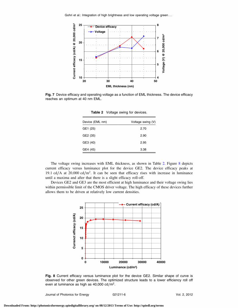
Figure 7 shows the device current efficacy and voltage at luminance of 20;000 cd∕m2 versusEML thickness. An increase in EML thickness from 25 to 45 nm leads to increase in operatingvoltage by 1.56 V. The device efficacy, however, shows a different behavior with thickness. Theefficacy increases from 15.7 cd∕A for GE1 to maximum of 21.6 cd∕A for GE3 and thendecreases to 18.3 cd∕A for GE4. It is likely that the charge imbalance in the device is reducedas thickness of EML is increased until 40 nm.
0 1 2 3 4 5 6 7 810-6
10-5
10-4
10-3
10-2
10-1
100
101
102
103
Lu
min
ance
(cd
/m²)
)²mc/
Am ( ytis
ned t
ner ru
C
Voltage (V)
GE1 GE2 GE3 GE4
102
103
104
105
Fig. 6 I-V-L characteristics for devices GE1, GE2, GE3, and GE4. The threshold voltage remainssimilar for all four devices but the turn-on voltage increases with increasing EML thickness.
Gohri et al.: Integration of high brightness and low operating voltage green : : :
Journal of Photonics for Energy 021211-5 Vol. 2, 2012
Downloaded From: http://photonicsforenergy.spiedigitallibrary.org/ on 08/12/2013 Terms of Use: http://spiedl.org/terms
The voltage swing increases with EML thickness, as shown in Table 2. Figure 8 depictscurrent efficacy versus luminance plot for the device GE2. The device efficacy peaks at19.1 cd∕A at 20;000 cd∕m2. It can be seen that efficacy rises with increase in luminanceuntil a maxima and after that there is a slight efficacy roll-off.
Devices GE2 and GE3 are the most efficient at high luminance and their voltage swing lieswithin permissible limit of the CMOS driver voltage. The high efficacy of these devices furtherallows them to be driven at relatively low current densities.
0 10000 20000 30000 400000
5
10
15
20
25
Cu
rren
ct e
ffic
acy
(cd
/A)
Luminance (cd/m²)
Current efficacy (cd/A)
Fig. 8 Current efficacy versus luminance plot for the device GE2. Similar shape of curve isobserved for other green devices. The optimized structure leads to a lower efficiency roll offeven at luminance as high as 40;000 cd∕m2.
20 30 40 5010
15
20
25Device efficacy
²m/
dc 000,02 @ )
A/dc( ycaciffe t
nerru
C
EML thickness (nm)
4
5
6
7
8
Voltage
Vo
ltag
e (V
) @
20,
000
cd/m
²
Fig. 7 Device efficacy and operating voltage as a function of EML thickness. The device efficacyreaches an optimum at 40 nm EML.
Table 2 Voltage swing for devices.
Device (EML nm) Voltage swing (V)
GE1 (25) 2.70
GE2 (35) 2.90
GE3 (40) 2.95
GE4 (45) 3.38
Gohri et al.: Integration of high brightness and low operating voltage green : : :
Journal of Photonics for Energy 021211-6 Vol. 2, 2012
Downloaded From: http://photonicsforenergy.spiedigitallibrary.org/ on 08/12/2013 Terms of Use: http://spiedl.org/terms
3.5 Device Lifetimes
The OLED lifetimes measured at constant current densities and are related to initial luminances11
by the Eq. (1):
LT50 × Lin ¼ k; (1)
where LT50 is the time required for 50% loss of initial luminance Li, k is constant, and n is theacceleration coefficient. To determine nwe measure the lifetime for the same test device but withvarying initial luminances. The log-log plot of LT50 versus Li is shown in Fig. 9. The absolutevalue of the slope is the n, which is 1.73 in the present case. The device lifetimes have beenmeasured in accelerated mode and device lifetimes have been extrapolated using Eq. (1). Thelifetimes for devices GE2 and GE3 are found to be 6000 and 8800 h, respectively, at5000 cd∕m2. These lifetimes are sufficient for practical application of these OLEDs in head-up displays within the constraint of low voltage CMOS substrate.
3.6 OLED Aging
To understand OLED aging, we examine whether the degradation is uniform in the EML or not.We construct a test device GT (Fig. 10) with similar structure to GE2 (Fig. 11), where only azone of width of 5 nm adjacent to EBL/EML interface is doped with green dopant. The rest ofEML still hosts the matrix but is undoped. The photoluminescence (PL) spectra of the two
Fig. 10 Device GT: EML doped with green in a 5 nm zone adjacent to EBL.
3,5 3,6 3,7 3,8 3,9 4,0 4,1 4,2 4,3 4,42
3
4
log
(LT
50)
log(Li)
Linear fit
Fig. 9 Log (Lifetime) versus log (initial luminance) is plotted to determine the accelerationcoefficient.
Gohri et al.: Integration of high brightness and low operating voltage green : : :
Journal of Photonics for Energy 021211-7 Vol. 2, 2012
Downloaded From: http://photonicsforenergy.spiedigitallibrary.org/ on 08/12/2013 Terms of Use: http://spiedl.org/terms
devices GT and GE2 is measured before (virgin) and after the lifetime test (with same initialluminance).
To get the PL spectra, light from 365 nm peak UV lamp is beamed in a small spot on top ofthe active area of the OLED. Figure 12 shows the PL spectra obtained. Further, the PL-luminanceof UV illuminated samples has been measured. In case of device GE2, the PL-luminance afterthe lifetime test is 75.5% of the virgin sample. Device GT shows the PL-luminance is decreasedto 64.5% of the virgin. The luminance loss is higher for device GT, which has a narrow dopedzone in EML. Table 3 shows the PL-luminance loss at same current efficacy loss for the twodevices.
400 500 600 7000,0
0,2
0,4
0,6
0,8
1,0
no
rm in
ten
sity
(a.
u.)
Wavelength (nm)
Virgin GE2 Aged GE2 Virgin GT Aged GT
Fig. 12 PL spectra of aged and virgin devices obtained by UV excitation. There is a small shoulderin the blue region for device GT which comes from the excitation of the blue host matrix. Thespectral intensity decrease of aged devices is more pronounced for device GT.
Table 3 Current efficacy (CE) and PL-Luminance loss for devices.
Measure
Aged device CE (loss %) P.L. (loss %)
GE2 50 24.5
GT 50 35.5
Fig. 11 Device GE2 with green doped EML.
Gohri et al.: Integration of high brightness and low operating voltage green : : :
Journal of Photonics for Energy 021211-8 Vol. 2, 2012
Downloaded From: http://photonicsforenergy.spiedigitallibrary.org/ on 08/12/2013 Terms of Use: http://spiedl.org/terms
It can be inferred that the emitter aging during lifetime is not uniform throughout the com-plete EML, but is rather strong near the recombination interface. Furthermore, this fact is alsojustified by observing the PL spectra for device GT. The origin of shoulder in blue region is dueto emission from the undoped EML. The decrease in height of the matrix shoulder after lifetimemeasurement is very low. On the contrary, the peak at 516 nm coming from green dopant emis-sion has decreased substantially in magnitude for the aged sample. The doped zone adjacent toEBL/EML interface sees high exciton densities owing to efficient transfer on energy from host togreen dopant. We believe the strong interaction of charge carriers with excitons at this interfaceresults in relatively stronger degradation around the interface. It is likely that emitter aging is notthe only cause of loss in luminance during lifetime as it does not account fully for the loss incurrent efficacy. Device aging can also result from loss in charge balance caused by degradationof blocker or charge transport materials or interfaces.
3.7 Microdisplay Perfomances
Furthermore, the green OLED stack GE1 has been integrated on an active matrix CMOS sub-strate to form a 5 megapixel microdisplay device MD1. The size of the display is 0.61″ diagonal,with a square subpixel of 5 μm. The voltage for local luminance of 20;000 cd∕m2 is measured tobe 5.6 V. The voltage swing for MD1 is 2.5 V for a contrast ratio of 1000. The electrical powerconsumption for MD1 is measured for high brightness mode (20;000 cd∕m2) and for dark imagemode (20 cd∕m2) and is found to be 487 and 0.49 mW, respectively.
4 Conclusion
We have demonstrated robust and highly efficient green OLEDs compatible with CMOS back-plane. The OLEDs are capable of operating at high luminance (20;000 cd∕m2) at voltages as lowas 5.6 V. The doped charge transport layers enable driving at high brightnesses with low bias.Optimizations are made to maximize the device efficacy, yielding an efficacy of 21.6 cd∕A at20;000 cd∕m2 for a device with 40 nm EML. The voltage swing and efficacy for devices canfurther be improved by using highly efficient phosphorescent emitter systems, such as EML. Theoptimized devices with 35 and 40 nm EML have a lifetime of 6000 and 8800 h, respectively, at ahigh brightness of 5000 cd∕m2. The long lifetime thereby enables practical application of OLEDbased microdisplays for high luminance head-up displays. Investigation into the aging of devicesshows that the degradation of emitter molecules is not uniform over the whole EML. Primarily,the zone in immediate vicinity of exciton recombination interface is responsible for lumi-nance loss.
References
1. C. W. Tang and S. A. VanSlyke, “Organic electroluminescent diodes,” Appl. Phys. Lett.51(12), 913–915 (1987), http://dx.doi.org/10.1063/1.98799.
3. G. Haas et al., “Novel high efficiency top emission OLEDs for display and lighting appli-cation,” SID Symposium Digest of Technical Papers 37(1), 1764–1766 (2006), http://dx.doi.org/10.1889/1.2433378
4. S. Reineke et al., “White organic light-emitting diodes with fluorescent tube efficiency,”Nature 459(7244), 234–238 (2009), http://dx.doi.org/10.1038/nature08003.
5. W. E. Howard and O. F. Prache, “Microdisplays based upon organic light-emitting diodes,”IBM J. Res. Dev. 45(1), 115–127 (2001), http://dx.doi.org/10.1147/rd.451.0115.
6. A. P. Ghosh et al., “Recent advances in small molecule OLED-on-silicon microdisplays,”Proc. SPIE 7415, 74150Q (2009), http://dx.doi.org/10.1117/12.829502.
7. B. Richter et al., “Bidirectional OLED microdisplay: combining display and image sensorfunctionality into a monolithic CMOS chip,” 2011 IEEE International Solid-State CircuitsConf., San Francisco Digest of Technical Papers, pp. 314–316 (2011).
Gohri et al.: Integration of high brightness and low operating voltage green : : :
Journal of Photonics for Energy 021211-9 Vol. 2, 2012
Downloaded From: http://photonicsforenergy.spiedigitallibrary.org/ on 08/12/2013 Terms of Use: http://spiedl.org/terms
8. G. Xie et al., “Highly efficient and low-cost top-emitting organic light-emitting diodes formonochromatic microdisplays,” Org. Electron. 11(3), 407–411 (2010), http://dx.doi.org/10.1016/j.orgel.2009.11.019.
9. T. A. Ali et al., “High performance top emitting green OLED micro-displays,” SID Sym-posium Digest of Technical Papers 40(1), 798–801 (2009), http://dx.doi.org/10.1889/1.3256910
10. X.-W. Chen et al., “Comprehensive analysis and optical design of top-emitting organiclight-emitting devices,” J. Appl. Phys. 101(11), 113107 (2007), http://dx.doi.org/10.1063/1.2739220.
11. C. Féry et al., “Physical mechanism responsible for the stretched exponential decaybehavior of aging organic light-emitting diodes,” Appl. Phys. Lett. 87(21), 213502 (2005),http://dx.doi.org/10.1063/1.2133922.
Biographies and photographs of the authors not available.
Gohri et al.: Integration of high brightness and low operating voltage green : : :
Journal of Photonics for Energy 021211-10 Vol. 2, 2012
Downloaded From: http://photonicsforenergy.spiedigitallibrary.org/ on 08/12/2013 Terms of Use: http://spiedl.org/terms