International Journal of u- and e- Service, Science and Technology Vol.9, No. 11 (2016), pp.105-120 http://dx.doi.org/10.14257/ijunesst.2016.9.11.10 ISSN: 2005-4246 IJUNESST Copyright ⓒ 2016 SERSC Integration of Standalone Solar Power System with Flying Capacitor Multilevel Inverter Contingent on Synchronous Sequential Circuit Rathinam Angamuthu 1 and Balaji Govindan 2 1 Department of Electrical and Electronics Engineering, Paavai Engineering College, Namakkal, Tamilnadu, India 2 Department of Electrical and Electronics Engineering, Paavai Engineering College, Namakkal, Tamilnadu, India Abstract The proposed system deals with the conversion of solar power into fundamental AC power by using flying capacitor multilevel inverter controlled by synchronous sequential circuits. The flying capacitor multilevel inverter controls the real and reactive power flow, deep voltage sags and short duration outages. The performance of the inverter is enhanced by using a synchronous sequential circuit, which gives the superior performance by reducing the total harmonic distortion in load voltage and capacitor voltage fluctuations. The synchronous sequential circuit based multilevel inverter offers several advantages like simpler structure, easy fault identification, cost-effectiveness and low power consumption. The performance of proposed strategy has been confirmed through simulation and hardware investigations. Keywords: Standalone solar power system, Flying capacitor multilevel inverter, Synchronous sequential circuits, Pulse width modulation, Total harmonic distortion 1. Introduction The total electrical energy consumption is increasing day by day. To meet this increasing demand, the electrical generating capacity has to be increased. Today the new capacity installation decisions are becoming complicated. However, that will need clean coal burning technologies that are fully acceptable to the public. An alternative to the coal burning, nuclear and fossil fuel power is renewable energy (hydro, wind, solar, biomass, geothermal and ocean). Hydroelectric projects have become difficult to realize because of the competing use of land and water. Among the other renewable power resources, wind and solar energy has recently experienced a rapid growth around the world. For remote villages outside two miles from the nearest transmission line, a stand-alone wind and solar energy system could be more economical [1]. After invention of the power electronic semiconductors, the controlling of power became easy in the field of generation, transmission, industrial motors and home appliances etc. The inverters are widely applied in the speed control of induction motors and standalone renewable energy systems like solar, fuel cell, magneto hydro dynamics etc. The two-level inverter has few limitations which are switching losses, constraint in the device rating and the EMI problem. In 1975 the multilevel inverters was introduce, which reduced the drawbacks of the two-level inverter and it has offered high voltage capability, low switching losses and reduced the harmonic. The multilevel inverter converts the DC into the staircase of AC. The staircase AC can be achieved by various
Transcript
International Journal of u- and e- Service, Science and Technology
Vol.9, No. 11 (2016), pp.105-120
http://dx.doi.org/10.14257/ijunesst.2016.9.11.10
ISSN: 2005-4246 IJUNESST
Copyright ⓒ 2016 SERSC
Integration of Standalone Solar Power System with Flying
Capacitor Multilevel Inverter Contingent on Synchronous
Sequential Circuit
Rathinam Angamuthu1 and Balaji Govindan
2
1Department of Electrical and Electronics Engineering,
Paavai Engineering College,
Namakkal, Tamilnadu, India 2Department of Electrical and Electronics Engineering,
Paavai Engineering College,
Namakkal, Tamilnadu, India
Abstract
The proposed system deals with the conversion of solar power into fundamental AC
power by using flying capacitor multilevel inverter controlled by synchronous sequential
circuits. The flying capacitor multilevel inverter controls the real and reactive power
flow, deep voltage sags and short duration outages. The performance of the inverter is
enhanced by using a synchronous sequential circuit, which gives the superior
performance by reducing the total harmonic distortion in load voltage and capacitor
voltage fluctuations. The synchronous sequential circuit based multilevel inverter offers
several advantages like simpler structure, easy fault identification, cost-effectiveness and
low power consumption. The performance of proposed strategy has been confirmed
through simulation and hardware investigations.
Keywords: Standalone solar power system, Flying capacitor multilevel inverter,
Synchronous sequential circuits, Pulse width modulation, Total harmonic distortion
1. Introduction
The total electrical energy consumption is increasing day by day. To meet this
increasing demand, the electrical generating capacity has to be increased. Today the new
capacity installation decisions are becoming complicated. However, that will need clean
coal burning technologies that are fully acceptable to the public. An alternative to the coal
burning, nuclear and fossil fuel power is renewable energy (hydro, wind, solar, biomass,
geothermal and ocean). Hydroelectric projects have become difficult to realize because of
the competing use of land and water. Among the other renewable power resources, wind
and solar energy has recently experienced a rapid growth around the world. For remote
villages outside two miles from the nearest transmission line, a stand-alone wind and solar
energy system could be more economical [1].
After invention of the power electronic semiconductors, the controlling of power
became easy in the field of generation, transmission, industrial motors and home
appliances etc. The inverters are widely applied in the speed control of induction motors
and standalone renewable energy systems like solar, fuel cell, magneto hydro dynamics
etc. The two-level inverter has few limitations which are switching losses, constraint in
the device rating and the EMI problem. In 1975 the multilevel inverters was introduce,
which reduced the drawbacks of the two-level inverter and it has offered high voltage
capability, low switching losses and reduced the harmonic. The multilevel inverter
converts the DC into the staircase of AC. The staircase AC can be achieved by various
International Journal of u- and e- Service, Science and Technology
Vol. 9, No. 11 (2016)
106 Copyright ⓒ 2016 SERSC
topologies of multilevel inverter, such as cascaded, diode clamp, flying capacitor
multilevel inverter (FCMLI) [2-4].
The n-level cascaded multilevel inverter requires a number of separate DC sources. A
series of power semiconductor switches with several DC sources are used and a staircase
AC waveform is synthesized. This is also called as multisource multilevel inverter [5].
The diode clamp multilevel inverter contains diodes and splitting capacitors, these
splitting capacitors and switching state combination produce the staircase AC [6]. Flying
capacitor multilevel inverter has flying capacitors and splitting capacitors. Due do the
combination of switching states and flying capacitors the inverter produce staircase AC
waveform. The diode clamp and flying capacitor multilevel inverters comes under the
category of single source multilevel inverter. The flying capacitor multilevel inverter
controls the real and reactive power but others cannot control the real and reactive power
[7-10].
The harmonic levels are controlled by using various kinds of switching techniques such
as single, multi and sinusoidal pulse width modulation techniques etc., [11-14]. The
digital system also plays a wider role for the control of power electronics; it is simple,
cost effective and improves the system performance.
The proposed system is focuses on the implementation of the synchronous sequential
circuit (SSC) to control a seven-level flying capacitor multilevel inverter for standalone
solar array system. The synchronous sequential circuit is a digital system which consists
of digital logic devices. The digital logic devices produce the PWM signals for controlling
the seven-level inverter. The proposed system is investigated through simulation and a
portable hardware model.
2. Introduction Standalone Solar System with Flying Capacitor
Multilevel Inverter
The solar array is mounted on a pole and the output DC supply from the array is
connected to the flying capacitor multilevel inverter. The different combination of flying
capacitors allows charging and discharging in order to produce the staircase AC
waveform from flying capacitor multilevel inverter. A seven-level flying capacitor
multilevel inverter circuit configuration with standalone solar array is shown in Figure 1.
This circuit configuration contains (n-1)(n-2)/2 flying capacitors (n-1) DC link
capacitors,(n-1) semiconductor switching devices, the inverter have(n-1)/2 upper and(n-
1)/2 lower side of semiconductor switching devices. The switches (S1, S1’) (S2, S2’) (S3, S-
3’) (S4, S4’) (S5, S5’) and (S6, S6’) are functioned with complementary manner like switch
S1 is ON, S1’is OFF and vice-versa [15].
Figure 1. Seven-Level Flying-Capacitor Multilevel Inverter with Standalone Solar Array
International Journal of u- and e- Service, Science and Technology
Vol. 9, No. 11 (2016)
Copyrightⓒ 2016 SERSC 107
This topology has a ladder structure of DC capacitors, the voltages in each leg of the
flying capacitors is different and they have been denoted as V1, V2, V3, V4 and V5.The
switching state of the flying capacitor multilevel inverter is shown in Table 1, it denotes
the sequence of switching and the corresponding voltage levels with respect to the neutral
point. With the implementation of the incremental voltage of adjacent flying capacitors
and the sequence of switching states, the stepped AC waveform is produced. In each
switching state the voltage polarity of flying capacitors position are changed as positive,
negative or no connection (NC) which is described in Table 2.
The main DC link capacitor voltage is Vdc, The inverter output voltage expressed as
2)()()()()( 6
16125234343452561
VVSVVSVVSVVSVVSVVSVo
(1)
Table 1. Switching State of Flying Capacitor Multilevel Inverter
The voltage of inner most capacitor is
1n
Vdc
(2)
The next innermost capacitor voltage is
1
2
11
n
V
n
V
n
V dcdcdc
(3)
Each flying capacitor leg voltage is incremented by
1n
Vdc
(4)
State
No. S6 S5 S4 S3 S2 S1 S6’ S5’ S4’ S3’ S2’ S1’
Volt
Level
1. ON ON ON ON ON ON OFF OFF OFF OFF OFF OFF vdc/2
2. ON ON ON ON ON OFF OFF OFF OFF OFF OFF ON Vdc/3
3. ON ON ON ON OFF ON OFF OFF OFF OFF ON OFF Vdc/3
4. ON ON ON OFF ON ON OFF OFF OFF ON OFF OFF Vdc/3
5. OFF OFF ON ON ON ON ON ON OFF OFF OFF OFF Vdc/6
6. OFF ON OFF ON ON ON ON OFF ON OFF OFF OFF Vdc/6
7. OFF ON ON OFF ON ON ON OFF OFF ON OFF OFF Vdc/6
8. OFF ON ON ON OFF OFF ON OFF OFF OFF ON ON 0
9. OFF OFF ON ON ON OFF ON ON OFF OFF OFF ON 0
10. OFF OFF OFF ON ON ON ON ON ON OFF OFF OFF 0
11. ON OFF OFF OFF OFF ON OFF ON ON ON ON OFF -Vdc/6
12. ON OFF OFF OFF ON OFF OFF ON ON ON OFF ON -Vdc/6
13. ON OFF OFF ON OFF OFF OFF ON ON OFF ON ON -Vdc/6
14. ON OFF OFF OFF OFF OFF OFF ON ON ON ON ON -Vdc/3
15. OFF ON OFF OFF OFF OFF ON OFF ON ON ON ON -Vdc/3
16. OFF OFF ON OFF OFF OFF ON ON OFF ON ON ON -Vdc/3
17. OFF OFF OFF OFF OFF OFF ON ON ON ON ON ON -Vdc/2
International Journal of u- and e- Service, Science and Technology
Vol. 9, No. 11 (2016)
108 Copyright ⓒ 2016 SERSC
Table 2. Status of Capacitor with Various Switching State
3. Designing of Synchronous Sequential Circuit
Almost all power electronic converters are operated in the switching mode. The
switches within the multilevel inverter are always turned either ON or OFF. The flow of
power in the multilevel inverter is controlled by changing the switches between these two
states, for this required switching pulses are designed by using a synchronous sequential
circuit. The proposed system is developed for standalone solar power system with seven-
level flying capacitor multilevel inverter; the level of voltage is decided by the switching
pulses of synchronous sequential circuit. The synchronous sequential circuits based
multilevel inverters offer several advantages like simple control of circuitry-level, ease of
formulation, etc. The following steps are followed as the designing procedure of clocked
sequential circuits [16-17].
This proposed system focuses on the seven-level output voltage; these levels converted
to equivalent binary numbers are as shown in Figure 2. The positive or the negative
waveform is being considered for designing because a sinusoidal waveform is a
symmetrical waveform. The equivalent decimal numbers of phase voltages are 0, 12, 14,
15, 6, and 4. P1, P2, P3 are the switching pulses of the inverter and AP is the auxiliary
switching pulse.
State
No.
C1 C2 C3 C4 C5 Voltage
Level
1. NC NC NC NC NC vdc/2
2. NC NC NC NC + Vdc/3
3. NC NC NC + - Vdc/3
4. NC NC + - NC Vdc/3
5. NC - NC NC NC Vdc/6
6. - + - NC NC Vdc/6
7. - NC + - NC Vdc/6
8. - NC NC + NC 0
9. NC - NC NC + 0
10. NC NC - NC NC 0
11. + NC NC NC - -Vdc/6
12. + NC NC - + -Vdc/6
13. + NC - + NC -Vdc/6
14. + NC NC NC NC -Vdc/3
15. - + NC NC NC -Vdc/3
16. NC - + NC NC -Vdc/3
17. NC NC NC NC NC -Vdc/2
International Journal of u- and e- Service, Science and Technology
Vol. 9, No. 11 (2016)
Copyrightⓒ 2016 SERSC 109
Figure 2. Seven-Level Voltage to Binary Conversion
The state diagram is drawn from the equivalent decimal numbers shown in Figure 2.
The state diagram provides another useful tool when the state of the entities in the system
will change in response to events. The next state of the state variables is assigned as the
order of equivalent binary of phase voltage as per Figure 3.This state diagram as acting as
a ring counter.
Figure 3. State Diagram
From the state diagram, the state table is developed and binary values are assigned to
each state in the state table. The JK flip flop is taken for designing the synchronous
sequential circuits. The JK flip flop excitation table is shown in Table 3, and the state
table of synchronous sequential circuit is shown in Table 4. Present state and next state of
state table has been derived from state diagram. In this state table the flip flop input of JA,
KA, JB, KB, JC, KC and JD, KD is developed from present state and next state of JK flip flop
excitation table.
Table 3. Excitation Table of JK Flip Flop
Q n Q n+1 J K
0 0 0 ×
0 1 1 ×
1 0 × 1
1 1 × 0
International Journal of u- and e- Service, Science and Technology
Vol. 9, No. 11 (2016)
110 Copyright ⓒ 2016 SERSC
Table 4. State Table
The Boolean function of synchronous sequential circuit has been determined from the
state Table 4.The K-map method has been implemented to find the Boolean function of
synchronous sequential circuit. In the K-maps plotted from Table 4, notice that the terms
which are having output 1, the corresponding cells marked as 1’s similarly other cells are
marked as zero’s and don’t care condition (×). The sum of product form of Boolean
expression can be plotted from the K-map, derivation of K-map are shown in Table 5 to
Table 12.
Table 5. K-Map for Find JA
C’D’ C’D CD CD’
A’B’ 1 × × ×
A’B 0 × × 0
AB × × × ×
AB’ × × × ×
JA = A’B’C’D’
Table 6. K-Map for Find KA
C’D’ C’D CD CD’
A’B’ × × × ×
A’B × × × ×
AB 0 × 1 0
AB’ × × × ×
KA = ABCD
Decimal
Number
Present State Next State Flip Flop
QA
QB
Q
C QD
QA
+1
QB+
1
QC
+1
QD
+1 JA KA JB KB JC KC JD KD
0 0 0 0 0 1 1 0 0 1 × 1 × 0 × 0 ×
1 0 0 0 1 × × × × × × × × × × × ×
2 0 0 1 0 × × × × × × × × × × × ×
3 0 0 1 1 × × × × × × × × × × × ×
4 0 1 0 0 0 0 0 0 × × × 1 0 × 0 ×
5 0 1 0 1 × × × × × × × × × × × ×
6 0 1 1 0 0 1 0 0 × × × 0 × 1 0 ×
7 0 1 1 1 × × × × × × × × × × × ×
8 1 0 0 0 × × × × × × × × × × × ×
9 1 0 0 1 × × × × × × × × × × × ×
10 1 0 1 0 × × × × × × × × × × × ×
11 1 0 1 1 × × × × × × × × × × × ×
12 1 1 0 0 1 1 1 0 × 0 × 0 1 × 0 ×
13 1 1 0 1 × × × × × × × × × × × ×
14 1 1 1 0 × × × × × 0 × 0 × 0 1 ×
15 1 1 1 1 0 1 1 0 × 1 × 0 × 0 × 1
International Journal of u- and e- Service, Science and Technology
Vol. 9, No. 11 (2016)
Copyrightⓒ 2016 SERSC 111
Table 7. K-Map for Find JB
C’D’ C’D CD CD’
A’B’ 1 × × ×
A’B × × × ×
AB × × × ×
AB’ × × × ×
JB= A’B’C’D’
Table 8. K-Map for Find KB
C’D’ C’D CD CD’
A’B’ × × × ×
A’B 1 × × 0
AB 0 × 0 0
AB’ × × × ×
KB = A’BC’D’
Table 9. K-Map for Find JC
Table 10. K-Map for Find KC
Table 11. K-Map for Find JD
C’D’ C’D CD CD’
A’B’ 0 × × ×
A’B 0 × × ×
AB 1 × × ×
AB’ × × × ×
JC = ABC’D’
C’D’ C’D CD CD’
A’B’ × × × ×
A’B × × × 1
AB × × 0 0
AB’ × × × ×
KC = A’BCD’
C’D’ C’D CD CD’
A’B’ 0 × × ×
A’B 0 × × 0
AB 0 × × 1
AB’ × × × ×
JD = ABCD’
International Journal of u- and e- Service, Science and Technology
Vol. 9, No. 11 (2016)
112 Copyright ⓒ 2016 SERSC
Table 12. K-Map for Find KD
From the derivation of K-Map (Table 5 to Table 12) Boolean expressions are
determined
JA = A’B’C’D’ (5)
KA = ABCD (6)
JB = A’B’C’D’ (7)
KB = A’BC’D’ (8)
JC = ABC’D’ (9)
KC = A’BCD’ (10)
JD = ABCD’ (11)
KD = ABCD (12)
4. Execution of Synchronous Sequential Circuit
The logical circuits based synchronous sequential circuit is designed from the Boolean
expression of equations 5 to 12 and the resultant logic circuit is shown in the Figure 4.
The synchronous sequential circuit contains JK flip flop (A, B, C, D), four input and
single output AND gate. The flip flop outputs are compliment function; it has high or low
output. Four input AND gate is connected based on the derivation of K-map and the
output of AND gate is connected to flip flop input as per Figure 4. The clock pulse
generator produces the sequence of square pulses, which is desired for seven-level flying
capacitor multilevel inverter fundamental frequency. The frequency of clock pulse
generator is 650Hz.
Figure 4. Synchronous Sequential Circuit
C’D’ C’D CD CD’
A’B’ × × × ×
A’B × × × ×
AB × × 1 ×
AB’ × × × ×
KD = ABCD
International Journal of u- and e- Service, Science and Technology
Vol. 9, No. 11 (2016)
Copyrightⓒ 2016 SERSC 113
The synchronous sequential circuit produces the sequence of switching pulses, this
sequence of pulses are used for both half cycles. The continuation of switching pulse is
broken up in every half cycle by using breakup logic circuits it has been shown in Figure
5. The breakup logic circuit consists of a flip flop and required clock pulse is taken from
the output QB of the flip flop-B.
The breakup logic circuit is designed from the possibility of switching state of flying
capacitor multilevel inverter; the following functions are used for breaking the sequence
of switching pulses
S1 = D’E’ (13)
S2 = C’E’ (14)
S3 = B’E’ (15)
S4 = DE’ (16)
S5 = CE’ (17)
S6 = BE’ (18)
Figure 5. Break Up Logic Circuits
5. Results and Discussion
In order to verify the proposed PWM method, the extensive system is carried out
through simulation and hardware. The digital modulation scheme based synchronous
sequential circuit switching pulses are shown in Figure 6a, and 6b, the separated
synchronous sequential circuit PWM and flying capacitor multilevel inverter switching
pulses are shown in Figure 7a, 7b, 7c, and 7d.
The separated six digital modulated PWM pulses are applied to seven-level multilevel
inverter upper semiconductor switching devices and by using NOT gate the upper
semiconductor switching’s pulses are inverted and the inverted switching pulses are given
to the lower semiconductor switching devices of the flying capacitor multilevel inverter.
The behavior of the proposed topology has been validated based on the simulation and a
prototype model. The prototype model has a solar panel, light load, clock pulse generator
which has 650Hz, IRF 540 MOSFET, and 3200µF capacitors.
Clock pulse and inverter output frequency are derived from
ICP FnF )1)2(( (19)
International Journal of u- and e- Service, Science and Technology
Vol. 9, No. 11 (2016)
114 Copyright ⓒ 2016 SERSC
)1)2((
n
FF CP
I (20)
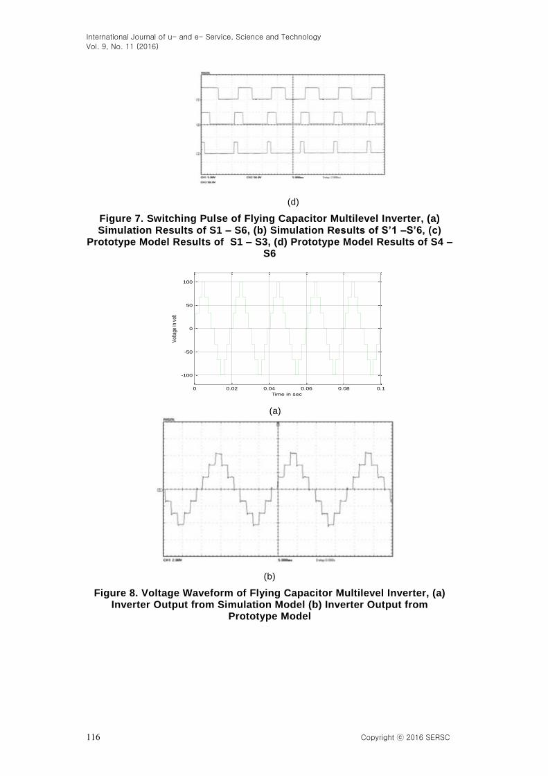
The valid digital modulated PWM switching combinations can synthesize a seven-level
output voltage, which is shown in Figure 8a, and 8b, Total Harmonic Distortion (THD) is
measured by using the digital analyzer it has shown in Figure 9a, and 9b. This
synchronous sequential circuit based flying capacitor multilevel inverter obtained the
output voltage 192V, frequency 50Hz and THD 16.7%. The experimental setup of
simulation and prototype model of seven-level flying capacitor multilevel inverter are
shown in Figure 10 and Figure 11 respectively.
0 0.02 0.04 0.06 0.08 0.10
0.5
1
1.5
0 0.02 0.04 0.06 0.08 0.10
0.5
1
1.5
0 0.02 0.04 0.06 0.08 0.10
0.5
1
1.5
0 0.02 0.04 0.06 0.08 0.10
0.5
1
1.5
Time in Sec
Voltage in V
olt
(a)
(b)
Figure 6. Switching Pulse of Synchronous Sequential Circuit, (a) Simulation Results of Clock Pulse, Flip Flop E, C, D (b) Prototype Model
Results of Flip Flop E, C, D
International Journal of u- and e- Service, Science and Technology
Vol. 9, No. 11 (2016)
Copyrightⓒ 2016 SERSC 115
0 0.02 0.04 0.06 0.08 0.10
0.51
1.5
0 0.02 0.04 0.06 0.08 0.10
0.51
1.5
0 0.02 0.04 0.06 0.08 0.10
0.51
1.5
0 0.02 0.04 0.06 0.08 0.10
0.51
1.5
0 0.02 0.04 0.06 0.08 0.10
0.51
1.5
0 0.02 0.04 0.06 0.08 0.10
0.51
1.5
Time in Sec
Voltage in V
olt
(a)
0 0.02 0.04 0.06 0.08 0.10
0.51
1.5
0 0.02 0.04 0.06 0.08 0.10
0.51
1.5
0 0.02 0.04 0.06 0.08 0.10
0.51
1.5
0 0.02 0.04 0.06 0.08 0.10
0.51
1.5
0 0.02 0.04 0.06 0.08 0.10
0.51
1.5
0 0.02 0.04 0.06 0.08 0.10
0.51
1.5
Time in Sec
Vol
tage
in V
olt
(b)
(c)
International Journal of u- and e- Service, Science and Technology
Vol. 9, No. 11 (2016)
116 Copyright ⓒ 2016 SERSC
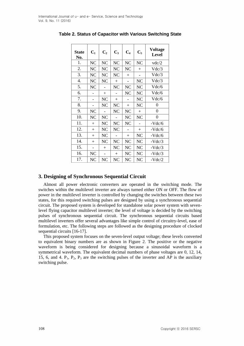
(d)
Figure 7. Switching Pulse of Flying Capacitor Multilevel Inverter, (a) Simulation Results of S1 – S6, (b) Simulation Results of S’1 –S’6, (c)
Prototype Model Results of S1 – S3, (d) Prototype Model Results of S4 – S6
0 0.02 0.04 0.06 0.08 0.1
-100
-50
0
50
100
Time in sec
Vol
tage
in v
olt
(a)
(b)
Figure 8. Voltage Waveform of Flying Capacitor Multilevel Inverter, (a) Inverter Output from Simulation Model (b) Inverter Output from
Prototype Model
International Journal of u- and e- Service, Science and Technology
Vol. 9, No. 11 (2016)
Copyrightⓒ 2016 SERSC 117
(a)
(b)
Figure 9. Total Harmonic Distortion of Voltage Waveform (a) THD Result of Simulation Model (b) THD Result of Prototype Model
International Journal of u- and e- Service, Science and Technology
Vol. 9, No. 11 (2016)
118 Copyright ⓒ 2016 SERSC
Figure 10. Experimental Setup of Simulation
Figure 11. Experimental Setup of Prototype Model
6. Comparative Study of SSC PWM and SHE PWM
The selective harmonic elimination pulse width modulation (SHE PWM) control
circuit of seven-level flying capacitor multilevel inverter is shown in Figure 12. The
control circuit consists of a RC phase shift oscillator, triangular wave generator, positive
clamping, negative clamping and comparator circuits. It has many numbers of active and
passive components. The fault identification of selective harmonic elimination PWM
control circuit is difficult compared to the synchronous sequential circuit (SSC). The
synchronous sequential circuit has digital logic devices, it is simple to identify the faults
International Journal of u- and e- Service, Science and Technology
Vol. 9, No. 11 (2016)
Copyrightⓒ 2016 SERSC 119
and easy to replace the logic devices. For standalone solar system, synchronous sequential
circuit based multilevel inverter has a simple structure, it is cost-effective, and it has low
power consumption and fast dynamic response.
Figure 12. Selective Harmonic Elimination PWM Circuits for Seven–Level FCMLI
7. Conclusion
This paper proposes a new switching topology designed for seven-level flying
capacitor multilevel inverter with standalone solar system, it provides the stepped
sinusoidal waveform and improves the behavior of the inverter and simplifies the
standalone solar system structure. Using this proposed method, the inverter fundamental
frequency can be also changed by changing the clock pulse generator’s frequency, the
calculation of switching angle is simple and less time consuming. The digital logic
algorithm can be implemented to different topology of multilevel inverter and n-level of
inverter can be designed easily. The future scope of this paper is to incorporate the
synchronous sequential circuit based multilevel inverter into a single chip using VLSI
technology.
References
[1] M. R. Patel, “Wind and Solar Power Systems”, 3rd ed. New York, NY, USA: CRC Press, (1999).
[2] N. S. Choi, J. G. Cho and G. H. Cho, “A general circuit topology of multilevel inverter”, In: IEEE 1991