Stitch aware detailed placement for multiple E-beam lithography
Yibo Lina,⁎, Bei Yub, Yi Zoua,c, Zhuo Lid, Charles J. Alpertd, David Z. Pana
a ECE Department, University of Texas at Austin, Austin, TX, USAb CSE Department, The Chinese University of Hong Kong, NT, Hong Kongc College of Engineering and Applied Sciences, Nanjing University, Nanjing, Chinad Cadence Design Systems, Inc., Austin, TX, USA
A R T I C L E I N F O
Keywords:Multiple electron beam lithographyStitch errorDetailed placementDynamic programming
A B S T R A C T
In multiple electron beam lithography (MEBL), a layout is split into stripes and the layout patterns are cut bystripe boundaries, then all the stripes are printed in parallel. If a via pattern or a vertical long wire is overlappingwith a stitch, it may suffer from poor printing quality due to the so called stitch error; then the circuitperformance may be degraded. In this paper, we propose a comprehensive study on the stitch aware detailedplacement to simultaneously minimize the stitch error and optimize traditional objectives, e.g., wirelength anddensity. Experimental results show that our algorithms are very effective on modified ICCAD 2014 benchmarksthat zero stitch error is guaranteed while the scaled half-perimeter wirelength is very comparable to a state-of-the-art detailed placer. In addition, our technique is very generic that it is applicable to many other placementtargets, such as local congestion optimization, which is also demonstrated in the experimental results.
1. Introductions
Due to the capability of accurate pattern generation, e-beamlithography (EBL) is a promising candidate for next generationlithography technologies for sub-14 nm nodes, along with othertechniques such as extreme ultra violet (EUV) and directed self-assembly (DSA) [1–3]. However, low throughput is still the bottleneckof an EBL system. Recently, an extended EBL technique, multiple e-beam lithography (MEBL), is proposed to improve manufacturingthroughput using parallel beam printing [4]. MEBL system utilizesthousands of parallel beams to write multiple layout patterns simulta-neously. Industry has already explored different MEBL implementa-tions and has demonstrated promising performance in terms of bothlithography accuracy and throughput [5,6].
In MEBL manufacturing process, a layout is split into stripes, andthe boundary between two touching stripes is defined as a stitch line.Each stripe has width of 50∼200 µm, and different stripes are printedsimultaneously through different electron beams. Although the parallelwriting scheme can dramatically improve the system throughput, italso introduces serious printability issues. That is, each stitch canintroduce so called stitch error, in an area with width around 15 nm[5]. If a pattern is overlapping with a stitch, it may suffer from poorprinting quality due to the stitch error. Therefore, if not carefullydesigned, due to the shape distortion, an MEBL system may confrontyield issue or even functional error.
We observe very significant shape distortions on via patterns and
long vertical wires. Fig. 1 shows two SEM images of shape distortion onvia layer and metal layer, respectively. In Fig. 1(a) we can see that allvias are very regular inside the beam stripes. However, at the stripeboundaries, the vias suffer from obvious distortions and irregularshrinking. In Fig. 1(b) we can see that the vertical wires are malformedin the stitch regions. Similar observations were also reported by Fanget al. [7] that the vertical wires are more susceptible to stitch errorsthan the horizontal wires.
There are several methods to minimize the impacts of stitch errorsfrom lithography perspective, e.g., avoiding dividing a critical patterninto adjacent sub-fields [8], using different field sizes [9], or reducingthe field size [10]. Recently, Fang et al. [7] considered the stitch errorduring detailed routing stage. However, detailed routing is a very latestage in physical design flow, thus there may exist some stitch errorsdifficult to be removed. For instance, stitch errors from vias dropped onpins of a standard cell cannot be optimized during routing stage. Thereare various detailed placement algorithms to address other emergingissues in advanced technology nodes, such as multiple patterninglithography [11–13], N10 design rules [14], multiple-row height cells[15–17], etc., which are summarized in [18].
In this work we propose a comprehensive study to consider thestitch error removal in detailed placement. We can directly optimizethe positions of both vias and intra-cell vertical wires. In addition, weconsider local congestion, thus a router (e.g. [7]) has more routingoptions to effectively remove stitch errors in higher metal layers. Fig. 2shows a placement example with three gates, where the density of
vertical metal1 segments varies from cell to cell. Some cells are moresusceptible to stitch errors as they have vertical wire segmentsdistributed at every site, while other cells have more space to avoidstitch errors. The comparison between Fig. 2(a) and Fig. 2(b) showsthat it is possible to smartly avoid stitch errors with small cellmovement.
To the best of our knowledge, this is the first work taking stitcherrors into consideration in placement stage. Our contributions aresummarized as follows.
• We propose a comprehensive detailed placement study to simulta-neously minimize the stitch error and optimize traditional objec-tives, e.g., wirelength and density.
• We develop a swap-based detailed placement engine with an optimalstitch aware single row placement.
• We present an nM( ) pruning technique to speed-up the single rowproblem, where n and M are number of cells in a row and maximumdisplacement respectively.
• Our pruning technique is very generic that it is applicable toconventional placement and other applications. We show that thepruning technique is also adjustable for local congestion optimiza-tion.
The rest of this paper is as follows. Section 2 introduces the stitchconstraints and the problem formulation. Section 3 explains theoptimization algorithms in detail. Section 4 lists the experimentalresults, followed by conclusion in Section 5.
2. Preliminaries and problem formulation
In an MEBL system, stitch lines repeat periodically with equalintervals. If a standard cell is not carefully placed and overlaps with onestitch line, it may suffer from stitch error. In this work we considerthree kinds of possible stitch errors, as follows. (1) Stitch over via: ifa via is cut by a stitch line, it can lead to potential disconnection. (2)Vertical routing: a vertical routing segment suffers more from stitch
lines than horizontal lines. (3) Short polygon: short horizontalrouting segment with vias may also result in problem.
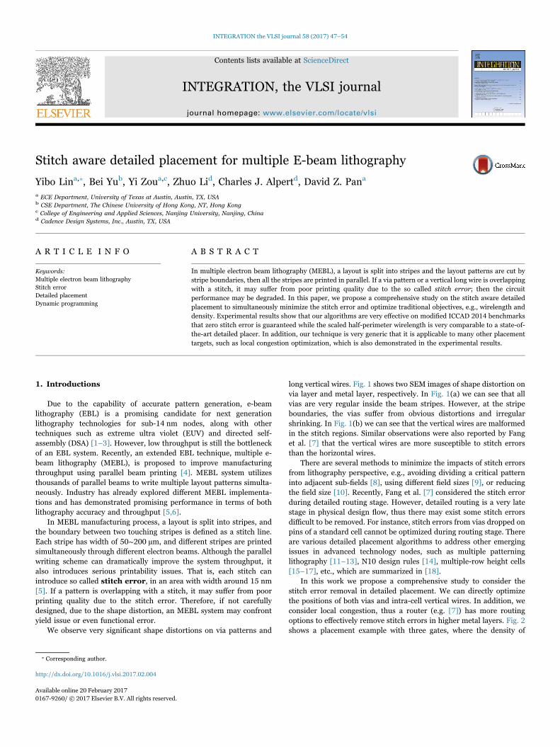
To accurately capture a stitch error, we partition each cell into siteswith width equal to the poly pitch. Since some intra-cell segments orvias are very susceptible to stitches, we note those sites covered bythese segments/vias as dangerous sites. For example, Fig. 3 shows thedangerous sites of cell BUF_X8. Note that for simplicity, here onlyintra-cell segments are illustrated. A stitch error happens if onedangerous site overlaps with an MEBL system stitch line.
This work adopts scaled half-perimeter wirelength (sHPWL) fromICCAD 2013 placement contest, defined as follows.
sHPWL HPWL α P= × (1 + × ),ABU (1)
where α is set to 1, and HPWL denotes half-perimeter wirelength.PABU represents ABU penalty to evaluate the placement congestion.Please refer to [19] for more details regarding the PABU calculation.
Problem 1 (Stitch Aware Detailed Placement). Given an initialdetailed placement with the information of dangerous sites for eachstandard cell, we seek a legal placement to minimize the stitch errorsand the sHPWL, simultaneously.
After solving Problem 1, we further perform a local congestionrefinement step to improve local routability and pin access withoutintroducing any additional stitch error and demonstrate the flexibilityof the proposed algorithm.
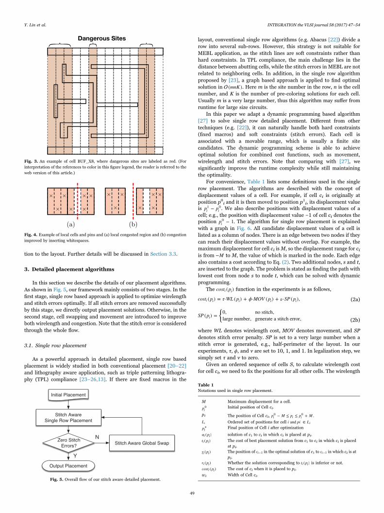
Problem 2 (Stitch Aware Local Congestion Refinement). Given adetailed placement solution without stitch errors, refine localcongestion while minimizing displacement without introducing anystitch error.
It should be noted that Problem 2 aims at smoothing congestedregions, as shown in Fig. 4 where cells are shown with dangerous sitesand pins are as cross marks. The region in Fig. 4(a) is very congesteddue to large number of pins in the region. We can insert whitespaces torelieve congestion in Fig. 4(b) while it is necessary to avoid stitch errorsat the same time. It is suitable to solve it by minimization of amaximum cost, which helps relieve congestion without large perturba-
Fig. 1. SEM images of stitch error for (a) via layer and (b) metal layer vertical wires.
Fig. 2. An example of (a) stitch errors in placement and (b) e-beam friendly placement.
Y. Lin et al. INTEGRATION the VLSI journal 58 (2017) 47–54
48
tion to the layout. Further details will be discussed in Section 3.3.
3. Detailed placement algorithms
In this section we describe the details of our placement algorithms.As shown in Fig. 5, our framework mainly consists of two stages. In thefirst stage, single row based approach is applied to optimize wirelengthand stitch errors optimally. If all stitch errors are removed successfullyby this stage, we directly output placement solutions. Otherwise, in thesecond stage, cell swapping and movement are introduced to improveboth wirelength and congestion. Note that the stitch error is consideredthrough the whole flow.
3.1. Single row placement
As a powerful approach in detailed placement, single row basedplacement is widely studied in both conventional placement [20–22]and lithography aware application, such as triple patterning lithogra-phy (TPL) compliance [23–26,13]. If there are fixed macros in the
layout, conventional single row algorithms (e.g. Abacus [22]) divide arow into several sub-rows. However, this strategy is not suitable forMEBL application, as the stitch lines are soft constraints rather thanhard constraints. In TPL compliance, the main challenge lies in thedistance between abutting cells, while the stitch errors in MEBL are notrelated to neighboring cells. In addition, in the single row algorithmproposed by [23], a graph based approach is applied to find optimalsolution in mnK( ). Here m is the site number in the row, n is the cellnumber, and K is the number of pre-coloring solutions for each cell.Usually m is a very large number, thus this algorithm may suffer fromruntime for large size circuits.
In this paper we adapt a dynamic programming based algorithm[27] to solve single row detailed placement. Different from othertechniques (e.g. [22]), it can naturally handle both hard constraints(fixed macros) and soft constraints (stitch errors). Each cell isassociated with a movable range, which is usually a finite sitecandidates. The dynamic programming scheme is able to achieveoptimal solution for combined cost functions, such as movement,wirelength and stitch errors. Note that comparing with [27], wesignificantly improve the runtime complexity while still maintainingthe optimality.
For convenience, Table 1 lists some definitions used in the singlerow placement. The algorithms are described with the concept ofdisplacement values of a cell. For example, if cell ci is originally atposition p0i and it is then moved to position p1i, its displacement valueis p p−i i
1 0. We also describe positions with displacement values of acell; e.g., the position with displacement value −1 of cell ci denotes theposition p − 1i
0 . The algorithm for single row placement is explainedwith a graph in Fig. 6. All candidate displacement values of a cell islisted as a column of nodes. There is an edge between two nodes if theycan reach their displacement values without overlap. For example, themaximum displacement for cell ci isM, so the displacement range for ciis from M− to M, the value of which is marked in the node. Each edgealso contains a cost according to Eq. (2). Two additional nodes, s and t,are inserted to the graph. The problem is stated as finding the path withlowest cost from node s to node t, which can be solved with dynamicprogramming.
The cost p( )i i function in the experiments is as follows,
cost p τ WL p ϕ MOV p ν SP p( ) = · ( ) + · ( ) + · ( ),i i i i i (2a)
⎧⎨⎩SP p( ) = 0, no stitch,large number, generate a stitch error,i
(2b)
where WL denotes wirelength cost, MOV denotes movement, and SPdenotes stitch error penalty. SP is set to a very large number when astitch error is generated, e.g., half-perimeter of the layout. In ourexperiments, τ, ϕ, and ν are set to 10, 1, and 1. In legalization step, wesimply set τ and ν to zero.
Given an ordered sequence of cells S, to calculate wirelength costfor cell ci, we need to fix the positions for all other cells. The wirelength
Fig. 3. An example of cell BUF_X8, where dangerous sites are labeled as red. (Forinterpretation of the references to color in this figure legend, the reader is referred to theweb version of this article.)
Fig. 4. Example of local cells and pins and (a) local congested region and (b) congestionimproved by inserting whitespaces.
Fig. 5. Overall flow of our stitch aware detailed placement.
Table 1Notations used in single row placement.
M Maximum displacement for a cell.
pi0 Initial position of Cell ci.
pi The position of Cell ci, p M p p M− ≤ ≤ +i i i0 0 .
Li Ordered set of positions for cell i pi Land ∈ i
p*l Final position of Cell i after optimization
α p( )i i solution of c1 to ci in which ci is placed at pi.
t p( )i i The cost of best placement solution from c1 to ci in which ci is placedat pi.
γ p( )i i The position of ci−1 in the optimal solution of c1 to ci−1 in which ci is atpi.
r p( )i i Whether the solution corresponding to t p( )i i is inferior or not.
cost p( )i i The cost of ci when it is placed to pi.
wi Width of Cell ci.
Y. Lin et al. INTEGRATION the VLSI journal 58 (2017) 47–54
49
cost is determined by the bounding boxes of nets. But if cell ci hasconnection to any cell in S, the wirelength cost for cell ci cannot bedetermined since cells in S are not fixed. To handle this, we introducethe wirelength model in [28] which ensures the wirelength cost for cellci is independent to other cells in S, while the optimality of thesolutions are maintained. If cell ci is connecting to any cell cj in the leftof cell ci in the same placement row, we regard the position of cj as theleft boundary of the row when computing the wirelength cost for ci.Similarly, if cell ci is connecting to any cell cj in the right of cell ci in thesame placement row, we regard the position of cj as the right boundaryof the row. This model is widely used in ordered single row placement,which turns out to be equivalent to HPWL [29,28].
We can see that function cost p( )i i is quite flexible, since we caninclude movement, wirelength and stitch errors. For hard constraintslike fixed macros, we only need to set its maximum displacement M tozero. For soft constraints like stitch lines, additional cost is applied if acell has overlap with them.
Lemma 1. Algorithm shown in Fig. 6 is optimal for cost function inEq. (2).
The proof is similar to that in [27], and is omitted here for brevity.The basic idea is that the optimal placement solution can be foundthrough a shortest path from s to t, and all the positions of cells can bederived from the displacement values of corresponding nodes. Sincethe constructed graph is a directed acyclic graph, the shortest path canbe calculated using topological traversal in nM( )2 steps, where n is thecell number in the row, and M is the maximum displacement for eachcell.
3.2. An nM( ) pruning algorithmThe runtime complexity of the above single row placement is
nM( )2 . When M is very large, the runtime becomes unacceptable.Here we propose a set of pruning techniques to achieve furtherspeedup, while still keeping the optimality. In addition, we cantheoretically prove that the runtime complexity can be improved from
nM( )2 to nM( ).
Algorithm 1. Single row placement with pruning
Require: A set of ordered cells c1 to cn of a row.Ensure: All the cells in the set are placed subjecting to optimal
objective function.1: L p M p M i to n← [ − , + ], ∀ = 1i i i
0 0 ;
2: t p cost p( ) ← ( )1 1 1 1 , p L∈1 1;3: t p( ) ← ∞i i , i to n← 2 , p L∈i i;
4: for each ci, i to n← 2 do5: N p M← −i−1
0 ;
6: for each p L∈i i do
7: for each p L∈i i−1 −1 where p N≥i−1 do
8: cost t p cost p← ( ) + ( )i i i i−1 −1 ;
9: if cost t p< ( )i i then
10: t p cost( ) ←i i ;
11: γ p p( ) ←i i i−1;
12: N p← i−1;
13: else14: break;15: end if16: end for17: end for18: Check inferior solutions and remove them from Li;19: end for20: cost ← ∞min ;21: for p p M p M∈ [ − , + ]n n n
0 0 do
22: if t p cost( ) <n n min then
23: cost t p← ( )min n n ;
24: p p* ←n n;
25: end if26: end for27: for i n← down to 2 do28: p γ p* ← ( )i i i−1 ;
29: end for
The details of our nM( ) implementation are shown in Algorithm 1.The main difference between the problems in [23,27] and our problemlies in the cost function. That is, the cost functions for a cell in theformer problems depend on other cells, such as the distance or coloringcost between two abutting cells, while the cost defined in Eq. (2) is onlyrelated to the cell itself; i.e., it is independent to any other cell. Due tothe independence in the cost function, we can minimize the total costwith nM( ) time complexity. Our speedup technique is generic that itcan also be applied into conventional detailed placement and legaliza-tion with an objective like wirelength or movement.
Lemma 2. Comparing two solutions α p( )i i and α q( )i i , if t p t q( ) ≥ ( )i i i iand p q≥i i, then α p( )i i is inferior to α q( )i i .
Proof. Suppose cell ci has two candidate positions pi and qi, wherep q≥i i and t p t q( ) ≥ ( )i i i i . Now consider any candidate position pi+1 forcell ci+1. If cell ci can be placed at pi without overlapping with cell ci+1,then qi is also a legal position for cell ci. We can always move cell cifrom pi to qi for better cost, because the total cost at cell ci+1 is theminimum value of t p cost p( ) + ( )i i i i+1 +1 . Therefore, solution α q( )i i isbetter than α p( )i i .□.
Lemma 2 corresponds to line 18 in Algorithm 1 where all inferiorsolutions are checked and skipped in the for loop. It implies thatt p t q( ) < ( )i i i i when p q>i i. Since the inferior solutions are removedfrom the set Li, we can assume there is no inferior solution in thefollow-up analysis.
If pi−1 introduces overlaps between cell ci−1 and ci, the cost isassigned to infinity. After skipping all inferior solutions, one shouldalso note that in line 9, the condition cost t p< ( )i i is always satisfiedwhen no overlapping occurs. The reason lies in that t p( )i i−1 −1 isdecreasing w.r.t pi−1 according to Lemma 2 and cost p( )i i does notchange in the for loop from line 7–16. So the else condition in line 13only happens when pi−1 results in overlaps, and we can break the loopunder such a condition.
Lemma 3. Let p*i−1 be the optimal position of cell ci−1 when cell ci is
placed at pi, and q*i−1 be the optimal position of cell ci−1 when cell ci is
placed at qi. If q p≥i i, then q p* ≥ *i i−1 −1.
Proof. For a legal position pi of cell ci, to minimize t p( )i i , we need tofind the smallest t p( )i i−1 −1 for all possible pi−1, because cost p( )i i hasbeen determined by pi. Let Pi−1 be the set of all legal values of pi−1 and
Fig. 6. Single row placement algorithm.
Y. Lin et al. INTEGRATION the VLSI journal 58 (2017) 47–54
50
Qi−1 denote all possible values of qi−1. Suppose p*i−1 is the best position
for cell ci−1 when ci is placed at pi and q*i−1 is the best position for cell
ci−1 when ci is placed at qi. Pi−1 and Qi−1 should share the same leftboundary l. Let Pi
r−1 be the right boundary of set Pi−1 and Qi
r−1 be the
right boundary of set Qi−1. Pir−1 is no larger than Qi
r−1, as q p≥i i. In other
words, we have P Q⊆i i−1 −1. The relationship can be rewritten as,
P p l p P p Q
q l q Q q P Q
= { | ≤ ≤ , ∈ Z},
= { | ≤ ≤ , ∈ Z}, ≤ .i i i i
ri i
i i ir
i ir
ir
−1 −1 −1 −1 −1 −1
−1 −1 −1 −1 −1 −1
If q*i−1 lies in the range between l and Pi
r−1, it must be equal to p*
i−1;otherwise, it is equal to some value between Pi
r−1 and Qi
r−1. Hence,
q p* ≥ *i i−1 −1.□
Lemma 3 corresponds to lines 5, 7 and 12 in Algorithm 1. Aftercomputing the optimal solution for cell ci at position p q=i , We canstart pi−1 from N (line 7 of Algorithm 1) instead of p M−i−1
0 to find anoptimal solution for a value p q>i . In line 7 and 12, for easierexplanation, we use N as a position, but in implementation we canstore the index of position in Li−1 to N such that the set Li−1 is accessedin constant time.
The above analysis guarantees the optimality of Algorithm 1.Compared with previous M( )2 algorithms in [27,23], Algorithm 1changes the complexity of the local search (from line 5 to line 18) to
M( ). Line 18 also takes M( ) time to check all inferior solutions andremove them. The runtime complexity of Algorithm 1 is nM( ).
Now we explain why the complexity of the local search (from line 5to line 18) is M( ) in Algorithm 1 with Fig. 6. The nature of the localsearch is to compute the best cost of cell c1 to ci for each position of cellci. Let N p( )i i denote the N value in line 7 to line 16 for position pi of cellci; in other words, N N p= ( )i i when we enter line 7. We also assumethere is no inferior solution for the computation of complexity for theworst case (inferior solutions are skipped anyway). Then the algorithmonly repeats the part of lines 8–15 by N p N p( + 1) − ( ) + 1i i i i times forposition pi of cell ci due to the update of N and early exit in line 14.Consider all the positions of cell ci from p M−i
0 to p M+i0 . It is
necessary to repeat the part of lines 8–15 by
∑ N p N p N p M N p M M
M M M
( + 1) − ( ) + 1 = ( + + 1) − ( − ) + 2
+ 1, =2 + 2 + 1, = ( ) times,
p p M
p M
i i i i i i i i= −
+0 0
i i
i
0
0
(3)
where we introduce N p M p M( − ) = −i i i0 0 and N p M p M( + + 1) = +i i i
0 0 forboundary conditions.
3.3. Flexibility of pruning techniques
In this section, we solve Problem 2 with an extension to the singlerow algorithm with pruning technique. It should be noted that ourpruning algorithm is flexible to any cost function cost p( )i i as long as itonly depends on pi itself. That is, it can be applied to speed-up the
conventional single row detailed placement problems [20–22].Furthermore, the cost function can also be extended from summa-
tion to maximization in line 8 of Algorithm 1. The application comesfrom the minimization of maximum displacement of cells whenoptimizing local congestion, where the cost function of each cell isadjusted from Eq. (2) to the following,
cost p p ϕ MOV p ν SP p τ GAP p p( , ) = · ( ) + · ( ) + · ( , ),i i i i i i i−1 −1 (4a)
GAP p p UB p p size( , ) = max(0, − ( − − )),i i i i i−1 −1 −1 (4b)
where GAP p p( , )i i−1 is the spacing cost between two neighboring cellsand UB is a user-defined upper bound for the spacing cost. The spacingcost can be more complicated such as that in [27] as long as the cost isnon-increasing with the increase of spacing, while we use a simpleversion for illustration. We switch the symbol of cost function fromcost p( )i i to cost p p( , )i i i−1 because the cost in Eq. (4) depends onpositions of both cell ci−1 and ci.
In Algorithm 1, line 8 is adjusted to,
cost t p cost p p← max( ( ), ( , )).i i i i i−1 −1 −1 (5)
It should be noted that enabling minimization of the maximum costensures small spacing and displacement cost of the worst case, whichfacilitates to solve Problem 2.
With the extension of cost function, it is not hard to see that Lemma2 still holds, which means we can still prune inferior solutions in lines18, but the correctness of early exit in line 14 needs to be explained.Due to the pruning of inferior solutions, t p( )i i−1 −1 is decreasing, whilecost p p( , )i i i−1 is non-decreasing (increasing) w.r.t pi−1. The maximiza-tion operation between a decreasing function and a non-decreasingfunction results in the fact that, given p*
i−1 as the best position, in theregion of p p≤ *i i−1 −1, t p cost p pmax ( ( ), ( , ))i i i i i−1 −1 −1 is non-increasing,while in the region of p p≥ *i i−1 −1, the cost is non-decreasing, shown asFig. 7. Therefore, it does not affect the results when exit early in line 14because p*
i−1 has been found.Lemma 3 needs additional proof under the new cost function. Let
p*i−1 be the best solution for t p( )i i . Then for any p p< *i i−1 −1,
t p cost p p t p t p cost p pmax( ( ), ( , )) = ( ) > max( ( * ), ( * , )),i i i i i i i i i i i i−1 −1 −1 −1 −1 −1 −1 −1 (6)
where the equality comes from the discussion in Fig. 7. For any q p>i iand p p< *i i−1 −1, we have following inequalities,
t p cost p q t p t p cost p p t pmax( ( ), ( , )) ≥ ( ) > max( ( * ), ( * , )) = ( ),i i i i i i i i i i i i i i−1 −1 −1 −1 −1 −1 −1 −1
(7)
which indicates that current solution of pi−1 and qi is inferior to α p( )i iwith p*
i−1 and qi. Therefore, we can directly start from p*i−1 when
searching for the best solution of t q( )i i . Although the condition ofoverlap is not mentioned, it can be integrated to the spacing cost, whichstill leads to non-decreasing cost function w.r.t pi−1. Hence the proofholds for the new cost function with maximization operation andspacing cost.
Fig. 7. Examples of maximization operation between a decreasing and a non-decreasing functions.
Y. Lin et al. INTEGRATION the VLSI journal 58 (2017) 47–54
51
3.4. Stitch aware global swap
In this step, the main objective is to optimize regions that containcells involved in stitch errors. After the optimization of single rowplacement, most stitch errors have been resolved. The remaining onesusually appear in highly congested placement bins. Therefore, we onlytry to move cells in such bins to alleviate the congestion and meanwhilereduce wirelength.
Due to the congestion of these regions, it is difficult to resolve themwith local perturbation such as reordering or sliding window. Thusglobal swap [28,30] is adopted where cells are allowed to moveanywhere within the displacement constraints. Generalized swap notonly enables swapping with cells but also white spaces, whichintegrates both swapping and moving strategies. The basic procedurefor cell swap is iteratively repeating the following three steps: (1) Selecta source cell to swap; (2) Identify optimal region for source cell; (3)Find the best cell or white space to swap with the source cell in theoptimal region.
In our implementation, we set the score function for swap asfollows,
score c c sHPWL λ P μ P( , ) = Δ − · − · ,i j ds ov (8)
where sHPWLΔ indicates sHPWL improvement, Pds indicates thepenalty for density increase of dangerous sites, and Pov is overlappenalty. Suppose cell ci is in bin Bi and cell cj belongs to bin Bj. Thearea of both bins is Ab. We define the density of dangerous sites as thenumber of dangerous sites over total amount of available sites in a bin.If a bin has overlap with any stitch line, we account only 70% of its totalsites as available. Let Dds(i) denote the density of dangerous sites inbin Bi before swap and D i′ ( )ds denote the density of dangerous sites inbin Bi after swap. Then we can define Pds with the following equation:
P D i D j D i D j A= max(0, | ′ ( ) − ′ ( )| − | ( ) − ( )|)· .ds ds ds ds ds b (9)
The overlap penalty is the area difference between the source cell andtarget cell or white space. If the target white space is larger than thesource cell, overlap penalty is zero. To achieve an equivalent numericscale to wirelength cost, Pds and Pov are divided by site half-perimeterin the implementation. In this way, all the costs have the same unit asdistance. λ and μ are set to 100. Only swapping attempt with bestpositive scores is accepted.
The scoring scheme proposed in Eq. (8) aims for balancing thedensity of cells and dangerous sites while improving wirelength.Although the penalty from ABU density is able to handle global densitydistribution, local control is necessary to avoid extremely denseregions. Furthermore, it is easier for a congested region with veryfew dangerous sites to find a stitch-error-free solution than that with alot of dangerous sites. Thus we introduce Pds as the additional penaltyfor such kind of regions. Since row-based legalization engine is applied,the height of bins for Pds is set to row height.
Overlap penalty is introduced to control the efforts during legaliza-tion. High legalization efforts will incur large displacement for somecells and thereby large wirelength degradation. Hence, after every 5000swaps, legalization algorithm will be performed to remove overlaps.Legalization algorithm is based on single-row placement (Section 3.1)with minimum movement as an objective.
We observe that the runtime for global swap is highly related to thecomplexity of score function. Considering that wirelength is included inthe calculation, it will be very slow to query the bounding box of largenets. Thus we develop a data structure in which pins of a net are storedas an ordered sequence according to pin positions. Cells in a row is keptin a linked-list [30] for fast cell swap and movement.
Usually a cell is connected to limited number of nets, thus its degreecan be treated as constant. Using the data structures above, it onlytakes constant time to query the bounding box and e(log ) to updatecell position in a net with e pins. Since score calculation happens muchmore frequent than actual cell swap or movement, faster score
calculation helps to reduce overall runtime. Let k be the number ofswapping candidates for a cell ci, we can achieve k( ) time complexityfor score calculation and e(log )max for cell position update if a swap ormovement is accepted, where emax is the maximum e of netsconnected to cell ci.
4. Experimental results
Our algorithms were implemented in C++ and tested on a 3.40 GHzLinux machine with 32 GB memory. Since traditional academicplacement benchmark suites has no intra-cell wire information, weintegrated the NanGate 15 nm standard cell library [31] into ICCAD2014 placement benchmarks [19]. ICCAD 2014 placement contestdefines two maximum displacement values for each benchmark, andwe choose the smaller ones for less perturbation to the originalplacements. We applied a state-of-the-art detailed placer, RippleDp[32], to generate the initial placement solutions. We scaled the bindimensions for ABU density analysis from the ICCAD 2014 bench-marks, so most generated test cases match to the number of bins in theoriginal ones. We pre-computed dangerous sites for all standard cellsin the library, which was served as input to our placer. We set the stripewidth of each single beam to 50 µm.
The metrics of the new benchmarks are shown in Table 2, wherecolumns “#cells” and “#nets” list the total cell number and net number,respectively. Besides, columns “#blk”, “dt” and “Disp.” represent theblockage (fixed macro) number, the target density, and the maximumdisplacement in um. Target density dt is necessary for computing ABUpenalty. Column “Util.” denotes the area utilizations of benchmarks.Note that test cases mgc_edit_dist, mgc_matrix_mult and net-card contain mixed-sized cells.
Table 3 lists the performance of our placer at different optimizationstages. The initial placement solutions (column “Init.”) are generatedby a traditional detailed placer, RippleDp [32], which aims at mini-mizing wirelength. As the state-of-the-art detailed placer, RippleDp canproduce very high quality placement solutions in terms of both HPWLand sHPWL. Here we set displacement constraint to be a very largenumber so that RippleDp can produce converged results. Column “SR”stands for single row placement, while column “Full Flow” denotesthe whole flow combining global swap and single row placement. Toevaluate the effectiveness of our algorithms, following metrics areintroduced. HPWL stands for half perimeter wirelength which is usedas a metric for wirelength. ST# represents the number of cells thatcontains stitch errors. It is measured by how many dangerous sites arecovered by the beam boundaries. Placement solutions with highcongestion are not desired, so we introduce sHPWL as discussed inSection 2. When measuring Runtime, which is the CPU run time inseconds, single thread is applied for consistency of results.
From Table 3 we can see that, with certain displacement con-straints, the proposed single row placement can achieve very goodefficacy in stitch error cancellation. That is, 99.9% of the initial stitcherrors are removed. Meanwhile, an average of 0.19% HPWL improve-ment and slight sHPWL increase are observed. However, for somecorner cases, such as leon2 and netcard, the single row placement isnot powerful enough due to the movement constraints from blockages
Table 2Benchmarks for Stitch Aware Placement.
Design #cells #nets #blk Util. dt Disp.
vga_lcd 165 K 165 K 0 68.94% 70% 10b19 219 K 219 K 0 44.85% 70% 20leon3mp 649 K 649 K 0 72.02% 75% 30leon2 794 K 795 K 0 84.19% 90% 40mgc_edit_dist (med) 131 K 133 K 13 67.26% 70% 30mgc_matrix_mult (mmm) 155 K 159 K 16 59.31% 65% 30netcard 959 K 961 K 12 66.29% 70% 50
Y. Lin et al. INTEGRATION the VLSI journal 58 (2017) 47–54
52
or congestions. Therefore, global swap is introduced as a follow-upoptimization step, and the corresponding results are shown in the lastcolumn. We can see that swapping cells between rows improvescongestion in dense regions and optimize wirelength. By applyingglobal swap together with single row algorithm, we are able to achievezero stitch errors for all test cases. As only small number of bins areconsidered for global swap, the runtime overhead can be neglected.Small changes in HPWL and sHPWL also indicate that the algorithmproduces little perturbation to initial placement.
It should be noted that the runtime of single row placement inTable 3 for case netcard is very close to that of leon2, while theformer has much larger cell number. The reason lies in those blockagesin netcard. That is, the runtime of single row placement is not onlyrelated to the number of cells, but also the amount of maximumdisplacement. Blockages have zero maximum displacement. So during
the propagation of candidate solutions in the dynamic programmingprocess, many infeasible solutions are automatically pruned. Therefore,the solution space has been significantly reduced and as a consequence,the best solution is found in shorter time.
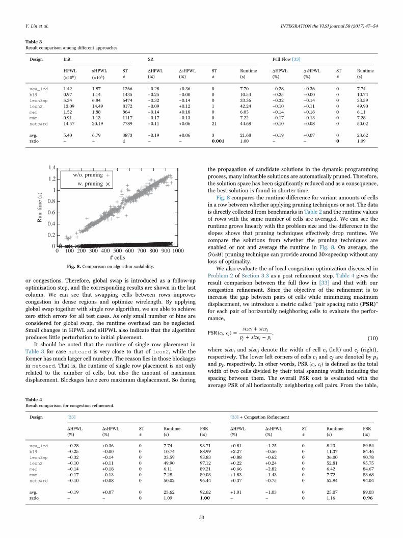
Fig. 8 compares the runtime difference for variant amounts of cellsin a row between whether applying pruning techniques or not. The datais directly collected from benchmarks in Table 2 and the runtime valuesof rows with the same number of cells are averaged. We can see theruntime grows linearly with the problem size and the difference in theslopes shows that pruning techniques effectively drop runtime. Wecompare the solutions from whether the pruning techniques areenabled or not and average the runtime in Fig. 8. On average, the
nM( ) pruning technique can provide around 30×speedup without anyloss of optimality.
We also evaluate the of local congestion optimization discussed inProblem 2 of Section 3.3 as a post refinement step. Table 4 gives theresult comparison between the full flow in [33] and that with ourcongestion refinement. Since the objective of the refinement is toincrease the gap between pairs of cells while minimizing maximumdisplacement, we introduce a metric called “pair spacing ratio (PSR)”for each pair of horizontally neighboring cells to evaluate the perfor-mance,
c csize size
p size pPSR( , ) =
++ −
,i ji j
j j i (10)
where sizei and sizej denote the width of cell ci (left) and cj (right),respectively. The lower left corners of cells ci and cj are denoted by piand pj, respectively. In other words, PSR c c( , )i j is defined as the totalwidth of two cells divided by their total spanning width including thespacing between them. The overall PSR cost is evaluated with theaverage PSR of all horizontally neighboring cell pairs. From the table,
Table 3Result comparison among different approaches.
Design Init. SR Full Flow [33]
HPWL sHPWL ST ΔHPWL ΔsHPWL ST Runtime ΔHPWL ΔsHPWL ST Runtime
Y. Lin et al. INTEGRATION the VLSI journal 58 (2017) 47–54
53
we can see that the congestion refinement is not only effective inremoving local congestion, but also smoothing the density, becauseboth PSR and sHPWL are improved by 4% and 1.1% compared withthe flow in [33], while no stitch errors occur. Although there isdegradation in HPWL, better density and local congestion are moreimportant for routability and final routed wirelength, considering theimprovement in sHPWL. In the refinement, we set the maximumdisplacement M to 10 to avoid large perturbation to the layout, whichalso speeds up the algorithm. As a consequence, there is only 7%runtime overhead. The weight for spacing cost is set to 10 in theexperiment and UB is set to the width of smaller cells in the cell pairs.
5. Conclusion
This work develops the first placement framework considering e-beam stitch errors during detailed placement stage. A linear-timesingle row placement algorithm is proposed with highly-adaptableobjective functions. Experimental results show its effectiveness in stitchcancellation while maintaining wirelength and congestion. With thecollaboration of stitch aware post-placement optimization such as [7],better manufactorability can be achieved. In addition, our highperformance pruning technique can be naturally embedded intoexisting physical design flow with different metrics (e.g., wirelength,routability, or congestion).
Acknowledgment
This work is supported in part by NSF (Project CCF-1218906),SRC (Project 2414.001) and CUHK Direct Grant for Research. Thanksto William Chow and Prof. F. Y. Young from CUHK for the updatedversion of RippleDp [32].
References
[1] D.Z. Pan, B. Yu, J.-R. Gao, Design for manufacturing with emerging nanolitho-graphy, IEEE Trans. Comput.-Aided Des. Integr. Circuits Syst. (TCAD) 32 (2013)1453–1472.
[2] D.Z. Pan, L. Liebmann, B. Yu, X. Xu, Y. Lin, Pushing multiple patterning in sub-10 nm: are we ready?, in: ACM/IEEE Design Automation Conference (DAC), 2015,pp. 197:1–197:6.
[3] B. Yu, X. Xu, S. Roy, Y. Lin, J. Ou, D.Z. Pan, Design for manufacturability andreliability in extreme-scaling VLSI, Sci. China Inf. Sci. (2016) 1–23.
[4] B.J. Lin, Future of multiple-e-beam direct-write systems, J. Micro/Nanolithogr.MEMS MOEMS (JM3) 11 (2012) (033011–1).
[5] C. Van den Berg, G. De Boer, S. Boschker, E. Hakkennes, G. Holgate, M. Hoving, R.Jager, J. Koning, V. Kuiper, Y. Ma, et al., Scanning exposures with a MAPPERmultibeam system, in: Proceedings of SPIE, volume 7970, 2011.
[6] M.A. McCord, P. Petric, U. Ummethala, A. Carroll, S. Kojima, L. Grella, S. Shriyan,C.T. Rettner, C.F. Bevis, REBL: design progress toward 16 nm half-pitch masklessprojection electron beam lithography, in: Proceedings of SPIE, volume 8323, 2012.
[8] K. Suzuki, T. Fujiwara, K. Hada, N. Hirayanagi, S. Kawata, K. Morita, K. Okamoto,T. Okino, S. Shimizu, T. Yahiro, Nikon EB stepper: its system concept andcountermeasures for critical issues, in: Proceedings of SPIE, volume 3997, 2000.
[9] D. Dougherty, R. Muller, P. Maker, S. Forouhar, Stitching-error reduction ingratings by shot-shifted electron-beam lithography, J. Lightw. Technol. 19 (2001)1527–1531.
[10] J. Albert, S. Theriault, F. Bilodeau, D. Johnson, K. Hill, P. Sixt, M. Rooks,
Minimization of phase errors in long fiber bragg grating phase masks made usingelectron beam lithography, IEEE Photonics Technol. Lett. 8 (1996) 1334–1336.
[11] B. Yu, X. Xu, J.-R. Gao, Y. Lin, Z. Li, C. Alpert, D.Z. Pan, Methodology for standardcell compliance and detailed placement for triple patterning lithography, IEEETrans. Comput.-Aided Des. Integr. Circuits Syst. (TCAD) 34 (2015) 726–739.
[13] Y. Lin, B. Yu, B. Xu, D.Z. Pan, Triple patterning aware detailed placement towardzero cross-row middle-of-line conflict, IEEE Trans. Comput.-Aided Des. Integr.Circuits Syst. (TCAD) (2017).
[14] K. Han, A.B. Kahng, H. Lee, Scalable detailed placement legalization for complexsub-14nm constraints, in: IEEE/ACM International Conference on Computer-Aided Design (ICCAD), 2015, pp. 867–873.
[15] G. Wu, C. Chu, Detailed placement algorithm for VLSI design with double-rowheight standard cells, IEEE Trans. Comput.-Aided Des. Integr. Circuits Syst.(TCAD) (2015).
[16] W.-K. Chow, C.-W. Pui, E.F.Y. Young, Legalization algorithm for multiple-rowheight standard cell design, in: ACM/IEEE Design Automation Conference (DAC),2016, pp. 83:1–83:6.
[17] Y. Lin, B. Yu, X. Xu, J.-R. Gao, N. Viswanathan, W.-H. Liu, Z. Li, C.J. Alpert, D.Z.Pan, MrDP: Multiple-row detailed placement of heterogeneous-sized cells foradvanced nodes, in: IEEE/ACM International Conference on Computer-AidedDesign (ICCAD), 2016a, pp. 7:1–7:8.
[18] Y. Lin, B. Yu, D. Z. Pan, Detailed placement in advanced technology nodes: asurvey, in: IEEE International Conference on Solid-State and Integrated CircuitTechnology (ICSICT), Hangzhou, China, 2016b, pp. 25–28.
[19] M.-C. Kim, J. Hu, N. Viswanathan, ICCAD-2014 CAD contest in incrementaltiming-driven placement and benchmark suite, in: IEEE/ACM InternationalConference on Computer-Aided Design (ICCAD), 2014, pp. 361–366.
[20] U. Brenner, J. Vygen, Faster optimal single-row placement with fixed ordering, in:IEEE/ACM Proceedings Design, Automation and Test in Eurpoe (DATE), 2000, pp.117–121.
[21] A.B. Kahng, I.L. Markov, S. Reda, On legalization of row-based placements, in:ACM Great Lakes Symposium on VLSI (GLSVLSI), 2004, pp. 214–219.
[22] P. Spindler, U. Schlichtmann, F.M. Johannes, Abacus: fast legalization of standardcell circuits with minimal movement, in: ACM International Symposium onPhysical Design (ISPD), 2008, pp. 47–53.
[23] B. Yu, X. Xu, J.-R. Gao, D.Z. Pan, Methodology for standard cell compliance anddetailed placement for triple patterning lithography, in: IEEE/ACM InternationalConference on Computer-Aided Design (ICCAD), 2013, pp. 349–356.
[24] J. Kuang, W.-K. Chow, E.F.Y. Young, Triple patterning lithography aware optimi-zation for standard cell based design, in: IEEE/ACM International Conference onComputer-Aided Design (ICCAD), 2014, pp. 108–115.
[25] T. Lin, C. Chu, TPL-aware displacement-driven detailed placement refinement withcoloring constraints, in: ACM International Symposium on Physical Design (ISPD),2015, pp. 75–80.
[26] Y. Lin, B. Yu, B. Xu, D.Z. Pan, Triple patterning aware detailed placement towardzero cross-row middle-of-line conflict, in: IEEE/ACM International Conference onComputer-Aided Design (ICCAD), 2015, pp. 396–403.
[27] T. Taghavi, C. Alpert, A. Huber, Z. Li, G.-J. Nam, S. Ramji, New placementprediction and mitigation techniques for local routing congestion, in: IEEE/ACMInternational Conference on Computer-Aided Design (ICCAD), 2010, pp. 621–624.
[28] M. Pan, N. Viswanathan, C. Chu, An efficient and effective detailed placementalgorithm, in: IEEE/ACM International Conference on Computer-Aided Design(ICCAD), 2005, pp. 48–55.
[29] A.B. Kahng, P. Tucker, A. Zelikovsky, Optimization of linear placements forwirelength minimization with free sites, in: IEEE/ACM Asia and South PacificDesign Automation Conference (ASPDAC), 1999, pp. 241–244.
[30] S. Popovych, H.-H. Lai, C.-M. Wang, Y.-L. Li, W.-H. Liu, T.-C. Wang, Density-aware detailed placement with instant legalization, in: ACM/IEEE DesignAutomation Conference (DAC), 2014, pp. 122:1–122:6.
[31] NanGate FreePDK15 Open Cell Library, ⟨http://www.nangate.com/?Page_id=2328⟩, 2015.
[32] W.-K. Chow, J. Kuang, X. He, W. Cai, E.F.Y. Young, Cell density-driven detailedplacement with displacement constraint, in: ACM International Symposium onPhysical Design (ISPD), 2014, pp. 3–10.
[33] Y. Lin, B. Yu, Y. Zou, Z. Li, C.J. Alpert, D.Z. Pan, Stitch aware detailed placementfor multiple e-beam lithography, in: IEEE/ACM Asia and South Pacific DesignAutomation Conference (ASPDAC), 2016, pp. 186–191.
Y. Lin et al. INTEGRATION the VLSI journal 58 (2017) 47–54