236
R Intel ® 955X Express Chipset Datasheet For the Intel ® 82955X Memory Controller Hub (MCH) April 2005 Document Number: 306828-001
R
Intel® 955X Express Chipset Datasheet
For the Intel® 82955X Memory Controller Hub (MCH) April 2005
Document Number: 306828-001
R
2 Intel® 82955X Memory Controller Hub (MCH) Datasheet
INFORMATION IN THIS DOCUMENT IS PROVIDED IN CONNECTION WITH INTEL® PRODUCTS. NO LICENSE, EXPRESS OR IMPLIED, BY ESTOPPEL OR OTHERWISE, TO ANY INTELLECTUAL PROPERTY RIGHTS IS GRANTED BY THIS DOCUMENT. EXCEPT AS PROVIDED IN INTEL’S TERMS AND CONDITIONS OF SALE FOR SUCH PRODUCTS, INTEL ASSUMES NO LIABILITY WHATSOEVER, AND INTEL DISCLAIMS ANY EXPRESS OR IMPLIED WARRANTY, RELATING TO SALE AND/OR USE OF INTEL PRODUCTS INCLUDING LIABILITY OR WARRANTIES RELATING TO FITNESS FOR A PARTICULAR PURPOSE, MERCHANTABILITY, OR INFRINGEMENT OF ANY PATENT, COPYRIGHT OR OTHER INTELLECTUAL PROPERTY RIGHT. Intel products are not intended for use in medical, life saving, or life sustaining applications.
Intel may make changes to specifications and product descriptions at any time, without notice.
Designers must not rely on the absence or characteristics of any features or instructions marked "reserved" or "undefined." Intel reserves these for future definition and shall have no responsibility whatsoever for conflicts or incompatibilities arising from future changes to them.
The Intel® 82955X Memory Controller Hub (MCH) may contain design defects or errors known as errata, which may cause the product to deviate from published specifications. Current characterized errata are available on request.
Contact your local Intel sales office or your distributor to obtain the latest specifications and before placing your product order. 1Hyper-Threading Technology requires a computer system with an Intel® Pentium® 4 processor supporting HT Technology and a Hyper-Threading Technology enabled chipset, BIOS and operating system. Performance will vary depending on the specific hardware and software you use. See http://www.intel.com/info/hyperthreading/ for more information including details on which processors support HT Technology.
Intel and Pentium are trademarks or registered trademarks of Intel Corporation or its subsidiaries in the United States and other countries.
*Other names and brands may be claimed as the property of others.
Copyright© 2005, Intel Corporation
R
Intel® 82955X Memory Controller Hub (MCH) Datasheet 3
Contents
1 Introduction ....................................................................................................................... 15 1.1 Terminology.......................................................................................................... 17 1.2 Reference Documents.......................................................................................... 18 1.3 MCH Overview ..................................................................................................... 19
1.3.1 Host Interface........................................................................................ 19 1.3.2 System Memory Interface..................................................................... 20 1.3.3 PCI Express* Graphics Interface.......................................................... 21 1.3.4 Direct Media Interface (DMI)................................................................. 22 1.3.5 System Interrupts.................................................................................. 22 1.3.6 MCH Clocking....................................................................................... 23 1.3.7 Power Management.............................................................................. 23
2 Signal Description .............................................................................................................25 2.1 Host Interface Signals .......................................................................................... 27 2.2 DDR2 DRAM Channel A Interface ....................................................................... 30 2.3 DDR2 DRAM Channel B Interface ....................................................................... 31 2.4 DDR2 DRAM Reference and Compensation....................................................... 32 2.5 PCI Express* Interface Signals ............................................................................ 32 2.6 Clocks, Reset, and Miscellaneous ....................................................................... 33 2.7 Direct Media Interface (DMI) ................................................................................ 33 2.8 Power, Ground ..................................................................................................... 34 2.9 Reset States and Pull-up/Pull-downs................................................................... 34
3 MCH Register Description ................................................................................................ 39 3.1 Register Terminology ........................................................................................... 40 3.2 Platform Configuration.......................................................................................... 41 3.3 Configuration Mechanisms................................................................................... 44
3.3.1 Standard PCI Configuration Mechanism .............................................. 44 3.3.2 PCI Express* Enhanced Configuration Mechanism............................. 44
3.4 Routing Configuration Accesses .......................................................................... 46 3.4.1 Internal Device Configuration Accesses............................................... 47 3.4.2 Bridge Related Configuration Accesses ............................................... 47
3.4.2.1 PCI Express* Configuration Accesses ................................ 47 3.4.2.2 DMI Configuration Accesses............................................... 48
3.5 I/O Mapped Registers .......................................................................................... 48 3.5.1 CONFIG_ADDRESS—Configuration Address Register ...................... 48 3.5.2 CONFIG_DATA—Configuration Data Register .................................... 50
4 Host Bridge Registers (D0:F0).......................................................................................... 51 4.1 Configuration Register Details (D1:F0) ................................................................ 53
4.1.1 VID—Vendor Identification (D0:F0) ...................................................... 53 4.1.2 DID—Device Identification (D0:F0) ...................................................... 53
R
4 Intel® 82955X Memory Controller Hub (MCH) Datasheet
4.1.3 PCICMD—PCI Command (D0:F0) ....................................................... 54 4.1.4 PCISTS—PCI Status (D0:F0)............................................................... 55 4.1.5 RID—Revision Identification (D0:F0).................................................... 56 4.1.6 CC—Class Code (D0:F0) ..................................................................... 57 4.1.7 MLT—Master Latency Timer (D0:F0)................................................... 57 4.1.8 HDR—Header Type (D0:F0) ................................................................ 58 4.1.9 SVID—Subsystem Vendor Identification (D0:F0)................................. 58 4.1.10 SID—Subsystem Identification (D0:F0)................................................ 58 4.1.11 CAPPTR—Capabilities Pointer (D0:F0) ............................................... 59 4.1.12 EPBAR—Egress Port Base Address (D0:F0) ...................................... 59 4.1.13 MCHBAR—MCH Memory Mapped Register Range Base Address
(D0:F0).................................................................................................. 60 4.1.14 PCIEXBAR—PCI Express* Register Range Base Address (D0:F0) ... 61 4.1.15 DMIBAR—Root Complex Register Range Base Address (D0:F0) ...... 63 4.1.16 DEVEN—Device Enable (D0:F0) ......................................................... 64 4.1.17 DEAP—DRAM Error Address Pointer (D0:F0)..................................... 64 4.1.18 DERRSYN— DRAM Error Syndrome (D0:F0) ..................................... 65 4.1.19 DERRDST—DRAM Error Destination (D0:F0)..................................... 66 4.1.20 PAM0—Programmable Attribute Map 0 (D0:F0) .................................. 67 4.1.21 PAM1—Programmable Attribute Map 1 (D0:F0) .................................. 68 4.1.22 PAM2—Programmable Attribute Map 2 (D0:F0) .................................. 68 4.1.23 PAM3—Programmable Attribute Map 3 (D0:F0) .................................. 69 4.1.24 PAM4—Programmable Attribute Map 4 (D0:F0) .................................. 69 4.1.25 PAM5—Programmable Attribute Map 5 (D0:F0) .................................. 70 4.1.26 PAM6—Programmable Attribute Map 6 (D0:F0) .................................. 70 4.1.27 LAC—Legacy Access Control (D0:F0) ................................................. 71 4.1.28 REMAPBASE—Remap Base Address (D0:F0) ................................... 73 4.1.29 REMAPLIMIT—Remap Limit Address (D0:F0) .................................... 73 4.1.30 TOLUD—Top of Low Usable DRAM (D0:F0) ....................................... 74 4.1.31 SMRAM—System Management RAM Control (D0:F0)........................ 75 4.1.32 ESMRAMC—Extended System Management RAM Control (D0:F0) .. 76 4.1.33 TOM—Top of Memory (D0:F0)............................................................. 77 4.1.34 ERRSTS—Error Status (D0:F0) ........................................................... 77 4.1.35 ERRCMD—Error Command (D0:F0) ................................................... 79 4.1.36 SMICMD—SMI Command (D0:F0) ...................................................... 80 4.1.37 SCICMD—SCI Command (D0:F0) ....................................................... 81 4.1.38 SKPD—Scratchpad Data (D0:F0) ........................................................ 81 4.1.39 CAPID0—Capability Identifier (D0:F0) ................................................. 82 4.1.40 EDEAP—Extended DRAM Error Address Pointer (D0:F0) .................. 82
4.2 MCHBAR Register ............................................................................................... 83 4.2.1 C0DRB0—Channel A DRAM Rank Boundary Address 0 .................... 84 4.2.2 C0DRB1—Channel A DRAM Rank Boundary Address 1 .................... 86 4.2.3 C0DRB2—Channel A DRAM Rank Boundary Address 2 .................... 86 4.2.4 C0DRB3—Channel A DRAM Rank Boundary Address 3 .................... 86 4.2.5 C0DRA0—Channel A DRAM Rank 0,1 Attribute ................................. 87 4.2.6 C0DRA2—Channel A DRAM Rank 2, 3 Attribute ................................ 87 4.2.7 C0DCLKDIS—Channel A DRAM Clock Disable .................................. 88 4.2.8 C0BNKARC—Channel A DRAM Bank Architecture ............................ 89 4.2.9 C0DRT1—Channel 0 DRAM Timing Register...................................... 90 4.2.10 C0DRC0—Channel 0 DRAM Controller Mode 0.................................. 91 4.2.11 C0DRC1—Channel 0 DRAM Controller Mode 1.................................. 93 4.2.12 C1DRB0—Channel B DRAM Rank Boundary Address 0 .................... 93 4.2.13 C1DRB1—Channel B DRAM Rank Boundary Address 1 .................... 93
R
Intel® 82955X Memory Controller Hub (MCH) Datasheet 5
4.2.14 C1DRB2—Channel B DRAM Rank Boundary Address 2 .................... 93 4.2.15 C1DRB3—Channel B DRAM Rank Boundary Address 3 .................... 94 4.2.16 C1DRA0—Channel B DRAM Rank 0,1 Attribute ................................. 94 4.2.17 C1DRA2—Channel B DRAM Rank 2,3 Attribute ................................. 94 4.2.18 C1DCLKDIS—Channel B DRAM Clock Disable .................................. 94 4.2.19 C1BNKARC—Channel B Bank Architecture ........................................ 95 4.2.20 C1DRT1—Channel 1 DRAM Timing Register 1................................... 95 4.2.21 C1DRC0—Channel 1 DRAM Controller Mode 0.................................. 95 4.2.22 C1DRC1—Channel 1 DRAM Controller Mode 1.................................. 95 4.2.23 PMCFG—Power Management Configuration ...................................... 96 4.2.24 PMSTS—Power Management Status .................................................. 96
4.3 EPBAR Registers—Egress Port Register Summary ........................................... 98 4.3.1 EPESD—EP Element Self Description................................................. 99 4.3.2 EPLE1D—EP Link Entry 1 Description .............................................. 100 4.3.3 EPLE1A—EP Link Entry 1 Address.................................................... 101 4.3.4 EPLE2D—EP Link Entry 2 Description .............................................. 101 4.3.5 EPLE2A—EP Link Entry 2 Address.................................................... 102
5 Host-PCI Express* Bridge Registers (D1:F0) ................................................................. 103 5.1 Configuration Register Details (D1:F0) .............................................................. 107
5.1.1 VID1—Vendor Identification (D1:F0) .................................................. 107 5.1.2 DID1—Device Identification (D1:F0) .................................................. 107 5.1.3 PCICMD1—PCI Command (D1:F0) ................................................... 108 5.1.4 PCISTS1—PCI Status (D1:F0)........................................................... 110 5.1.5 RID1—Revision Identification (D1:F0)................................................ 111 5.1.6 CC1—Class Code (D1:F0) ................................................................. 111 5.1.7 CL1—Cache Line Size (D1:F0) .......................................................... 112 5.1.8 HDR1—Header Type (D1:F0) ............................................................ 112 5.1.9 PBUSN1—Primary Bus Number (D1:F0) ........................................... 112 5.1.10 SBUSN1—Secondary Bus Number (D1:F0) ...................................... 113 5.1.11 SUBUSN1—Subordinate Bus Number (D1:F0) ................................. 113 5.1.12 IOBASE1—I/O Base Address (D1:F0) ............................................... 114 5.1.13 IOLIMIT1—I/O Limit Address (D1:F0) ................................................ 114 5.1.14 SSTS1—Secondary Status (D1:F0) ................................................... 115 5.1.15 MBASE1—Memory Base Address (D1:F0)........................................ 116 5.1.16 MLIMIT1—Memory Limit Address (D1:F0)......................................... 117 5.1.17 PMBASE1—Prefetchable Memory Base Address (D1:F0) ................ 118 5.1.18 PMLIMIT1—Prefetchable Memory Limit Address (D1:F0) ................. 119 5.1.19 PMBASEU1—Prefetchable Memory Base Address........................... 120 5.1.20 PMLIMITU1— Prefetchable Memory Limit Address........................... 121 5.1.21 CAPPTR1—Capabilities Pointer (D1:F0) ........................................... 122 5.1.22 INTRLINE1—Interrupt Line (D1:F0) ................................................... 122 5.1.23 INTRPIN1—Interrupt Pin (D1:F0) ....................................................... 122 5.1.24 BCTRL1—Bridge Control (D1:F0) ...................................................... 123 5.1.25 PM_CAPID1—Power Management Capabilities (D1:F0) .................. 125 5.1.26 PM_CS1—Power Management Control/Status (D1:F0) .................... 126 5.1.27 SS_CAPID—Subsystem ID and Vendor ID Capabilities (D1:F0) ...... 127 5.1.28 SS—Subsystem ID and Subsystem Vendor ID (D1:F0) .................... 127 5.1.29 MSI_CAPID—Message Signaled Interrupts Capability ID (D1:F0).... 128 5.1.30 MC—Message Control (D1:F0) .......................................................... 129 5.1.31 MA—Message Address (D1:F0)......................................................... 130 5.1.32 MD—Message Data (D1:F0) .............................................................. 130 5.1.33 PCI_EXPRESS_CAPL—PCI Express* Capability List (D1:F0) ......... 131
R
6 Intel® 82955X Memory Controller Hub (MCH) Datasheet
5.1.34 PCI_EXPRESS _CAP—PCI Express* Capabilities (D1:F0) .............. 131 5.1.35 DCAP—Device Capabilities (D1:F0) .................................................. 132 5.1.36 DCTL—Device Control (D1:F0).......................................................... 133 5.1.37 DSTS—Device Status (D1:F0) ........................................................... 134 5.1.38 LCAP—Link Capabilities (D1:F0) ....................................................... 135 5.1.39 LCTL—Link Control (D1:F0) ............................................................... 136 5.1.40 LSTS—Link Status (D1:F0) ................................................................ 137 5.1.41 SLOTCAP—Slot Capabilities (D1:F0) ................................................ 138 5.1.42 SLOTCTL—Slot Control (D1:F0) ........................................................ 140 5.1.43 SLOTSTS—Slot Status (D1:F0) ......................................................... 141 5.1.44 RCTL—Root Control (D1:F0) ............................................................. 142 5.1.45 RSTS—Root Status (D1:F0)............................................................... 143 5.1.46 PCI_EXPRESS_LC—PCI Express* Legacy Control (D1:F0) ............ 144 5.1.47 VCECH—Virtual Channel Enhanced Capability Header (D1:F0) ...... 145 5.1.48 PVCCAP1—Port VC Capability Register 1 (D1:F0) ........................... 145 5.1.49 PVCCAP2—Port VC Capability Register 2 (D1:F0) ........................... 146 5.1.50 PVCCTL—Port VC Control (D1:F0) ................................................... 146 5.1.51 VC0RCAP—VC0 Resource Capability (D1:F0) ................................. 147 5.1.52 VC0RCTL—VC0 Resource Control (D1:F0) ...................................... 147 5.1.53 VC0RSTS—VC0 Resource Status (D1:F0)........................................ 148 5.1.54 VC1RCAP—VC1 Resource Capability (D1:F0) ................................. 148 5.1.55 VC1RCTL—VC1 Resource Control (D1:F0) ...................................... 149 5.1.56 VC1RSTS—VC1 Resource Status (D1:F0)........................................ 150 5.1.57 RCLDECH—Root Complex Link Declaration Enhanced Capability
Header (D1:F0) ................................................................................... 150 5.1.58 ESD—Element Self Description (D1:F0) ............................................ 151 5.1.59 LE1D—Link Entry 1 Description (D1:F0)............................................ 152 5.1.60 LE1A—Link Entry 1 Address (D1:F0)................................................. 152 5.1.61 UESTS—Uncorrectable Error Status (D1:F0) .................................... 153 5.1.62 UEMSK—Uncorrectable Error Mask (D1:F0)..................................... 154 5.1.63 CESTS—Correctable Error Status (D1:F0) ........................................ 155 5.1.64 CEMSK—Correctable Error Mask (D1:F0)......................................... 156 5.1.65 PEGSSTS—PCI Express* Sequence Status (D1:F0)........................ 157
6 Direct Media Interface (DMI) RCRB................................................................................ 159 6.1 DMI RCRB Configuration Register Details......................................................... 160
6.1.1 DMIVCECH—DMI Virtual Channel Enhanced Capability Header ..... 160 6.1.2 DMIPVCCAP1—DMI Port VC Capability Register 1 .......................... 160 6.1.3 DMIPVCCAP2—DMI Port VC Capability Register 2 .......................... 161 6.1.4 DMIPVCCTL—DMI Port VC Control .................................................. 161 6.1.5 DMIVC0RCAP—DMI VC0 Resource Capability ................................ 162 6.1.6 DMIVC0RCTL0—DMI VC0 Resource Control ................................... 162 6.1.7 DMIVC0RSTS—DMI VC0 Resource Status....................................... 163 6.1.8 DMIVC1RCAP—DMI VC1 Resource Capability ................................ 163 6.1.9 DMIVC1RCTL1—DMI VC1 Resource Control ................................... 164 6.1.10 DMIVC1RSTS—DMI VC1 Resource Status....................................... 164 6.1.11 DMILCAP—DMI Link Capabilities ...................................................... 165 6.1.12 DMILCTL—DMI Link Control .............................................................. 165 6.1.13 DMILSTS—DMI Link Status ............................................................... 166 6.1.14 DMIUESTS—DMI Uncorrectable Error Status ................................... 167 6.1.15 DMIUEMSK—DMI Uncorrectable Error Mask.................................... 168 6.1.16 DMICESTS— DMI Correctable Error Status ...................................... 169
R
Intel® 82955X Memory Controller Hub (MCH) Datasheet 7
7 System Address Map...................................................................................................... 171 7.1 Legacy Address Range ...................................................................................... 173
7.1.1 DOS Range (0h–9_FFFFh) ................................................................ 173 7.1.2 Legacy Video Area (A_0000h–B_FFFFh) .......................................... 174 7.1.3 Expansion Area (C_0000h–D_FFFFh)............................................... 174 7.1.4 Extended System BIOS Area (E_0000h–E_FFFFh) .......................... 175 7.1.5 System BIOS Area (F_0000h–F_FFFFh)........................................... 175 7.1.6 Programmable Attribute Map (PAM) Memory Area Details................ 175
7.2 Main Memory Address Range (1 MB to TOLUD) ..............................................176 7.2.1 ISA Hole (15 MB–16 MB) ................................................................... 177 7.2.2 TSEG .................................................................................................. 178 7.2.3 Pre-allocated Memory......................................................................... 178
7.3 PCI Memory Address Range (TOLUD–4 GB) ................................................... 178 7.3.1 APIC Configuration Space (FEC0_0000h–FECF_FFFFh)................. 179 7.3.2 HSEG (FEDA_0000h–FEDB_FFFFh) ................................................ 180 7.3.3 FSB Interrupt Memory Space (FEE0_0000–FEEF_FFFF) ................ 180 7.3.4 High BIOS Area .................................................................................. 180
7.4 Main Memory Address Space (4 GB to Remaplimit) ......................................... 180 7.4.1 Memory Re-claim Background ........................................................... 181 7.4.2 Memory Re-mapping .......................................................................... 181 7.4.3 PCI Express* Configuration Address Space ...................................... 182 7.4.4 PCI Express* Graphics Attach............................................................ 182 7.4.5 AGP DRAM Graphics Aperture .......................................................... 182
7.5 System Management Mode (SMM) ................................................................... 183 7.5.1 SMM Space Definition ........................................................................ 183 7.5.2 SMM Space Restrictions ....................................................................184 7.5.3 SMM Space Combinations ................................................................. 184 7.5.4 SMM Control Combinations................................................................ 184 7.5.5 SMM Space Decode and Transaction Handling ................................ 185 7.5.6 Processor WB Transaction to an Enabled SMM Address Space ...... 185 7.5.7 Memory Shadowing ............................................................................ 185 7.5.8 I/O Address Space.............................................................................. 185 7.5.9 PCI Express* I/O Address Mapping ................................................... 186 7.5.10 MCH Decode Rules and Cross-Bridge Address Mapping ................. 186 7.5.11 Legacy VGA and I/O Range Decode Rules ....................................... 186
8 Functional Description .................................................................................................... 187 8.1 Host Interface ..................................................................................................... 187
8.1.1 FSB IOQ Depth................................................................................... 187 8.1.2 FSB OOQ Depth ................................................................................. 187 8.1.3 FSB GTL+ Termination....................................................................... 187 8.1.4 FSB Dynamic Bus Inversion ............................................................... 187
8.1.4.1 APIC Cluster Mode Support .............................................. 188 8.2 System Memory Controller................................................................................. 189
8.2.1 System Memory Configuration Registers Overview........................... 190 8.2.2 DRAM Technologies and Organization .............................................. 191
8.2.2.1 Rules for Populating DIMM Slots ...................................... 191 8.2.2.2 System Memory Supported Configurations ...................... 191 8.2.2.3 Main Memory DRAM Address Translation and Decoding 192 8.2.2.4 ECC Support ..................................................................... 194
8.2.3 DRAM Clock Generation .................................................................... 194 8.2.4 Suspend To RAM and Resume.......................................................... 194
R
8 Intel® 82955X Memory Controller Hub (MCH) Datasheet
8.2.5 DDR2 On Die Termination.................................................................. 194 8.3 PCI Express* ...................................................................................................... 195
8.3.1 PCI Express* Architecture .................................................................. 195 8.3.1.1 Transaction Layer.............................................................. 195 8.3.1.2 Data Link Layer ................................................................. 195 8.3.1.3 Physical Layer ................................................................... 195
8.4 Power Management ........................................................................................... 196 8.5 Clocking.............................................................................................................. 196
9 Electrical Characteristics................................................................................................. 199 9.1 Absolute Minimum and Maximum Ratings......................................................... 199 9.2 Power Characteristics ........................................................................................ 201 9.3 Signal Groups.....................................................................................................202 9.4 DC Characteristics ............................................................................................. 204
10 Ballout and Package Information .................................................................................... 207 10.1 Ballout................................................................................................................. 207 10.2 Package.............................................................................................................. 223
11 Testability ........................................................................................................................ 225 11.1 Complimentary Pins ........................................................................................... 225 11.2 XOR Test Mode Initialization.............................................................................. 226 11.3 XOR Chain Definition ......................................................................................... 227 11.4 XOR Chains........................................................................................................ 227 11.5 PADs Excluded from XOR Mode(s) ...................................................................236
R
Intel® 82955X Memory Controller Hub (MCH) Datasheet 9
Figures Figure 1-1. Intel® 955X Express Chipset System Block Diagram Example ..................... 16 Figure 2-1. Signal Information Diagram............................................................................ 26 Figure 3-1. Conceptual Intel® 955X Express Chipset Platform PCI Configuration Diagram42 Figure 3-2. Register Organization..................................................................................... 43 Figure 3-3. Memory Map to PCI Express* Device Configuration Space .......................... 45 Figure 3-4. MCH Configuration Cycle Flow Chart ............................................................ 46 Figure 4-1. Link Declaration Topology.............................................................................. 98 Figure 7-1. System Address Ranges.............................................................................. 172 Figure 7-2. Microsoft MS-DOS* Legacy Address Range ............................................... 173 Figure 7-3. Main Memory Address Range...................................................................... 177 Figure 7-4. PCI Memory Address Range........................................................................ 179 Figure 8-1. System Memory Styles................................................................................. 190 Figure 8-2. Platform Clocking Example .......................................................................... 197 Figure 10-1. Intel® 82955X MCH Ballout Diagram (Top View – Columns 43–30).......... 208 Figure 10-2. Intel® 82955X MCH Ballout Diagram (Top View – Columns 29–16).......... 209 Figure 10-3. Intel® 82955X MCH Ballout Diagram (Top View – Columns 15–1)............ 210 Figure 10-4. MCH Package Dimensions (Top View)...................................................... 223 Figure 10-5. MCH Package Dimensions (Side View)..................................................... 223 Figure 10-6. MCH Package Dimensions (Bottom View)................................................. 224 Figure 11-1. XOR Test Mode Initialization Cycles .......................................................... 226
R
10 Intel® 82955X Memory Controller Hub (MCH) Datasheet
Tables Table 4-1. Host Bridge Register Address Map (D0:F0).................................................... 51 Table 4-2. MCHBAR Register Address Map .................................................................... 83 Table 4-3. Egress Port Register Address Map ................................................................. 98 Table 5-1. Host-PCI Express* Graphics Bridge Register Address Map (D1:F0) ........... 103 Table 6-1. DMI Register Address Map ........................................................................... 159 Table 7-1. Expansion Area Memory Segments .............................................................. 175 Table 7-2. Extended System BIOS Area Memory Segments......................................... 175 Table 7-3. System BIOS Area Memory Segments ......................................................... 175 Table 7-4. Pre-Allocated Memory Example for 64-MB DRAM, 1-MB VGA and 1-MB
TSEG ....................................................................................................................... 178 Table 7-5. SMM Space ................................................................................................... 184 Table 7-6. SMM Control .................................................................................................. 185 Table 8-1. Sample System Memory Organization with Interleaved Channels ............... 189 Table 8-2. Sample System Memory Organization with Asymmetric Channels .............. 189 Table 8-3. DDR2 DIMM Supported Configurations ........................................................ 192 Table 8-4. DRAM Address Translation (Single Channel/Dual Asymmetric Mode) ........ 193 Table 8-5. DRAM Address Translation (Dual Channel Symmetric Mode) ..................... 193 Table 9-1. Absolute Minimum and Maximum Ratings .................................................... 200 Table 9-2. Non Memory Power Characteristics .............................................................. 201 Table 9-3. DDR2 Power Characteristics......................................................................... 201 Table 9-4. Signal Groups ................................................................................................ 202 Table 9-5. DC Characteristics......................................................................................... 204 Table 10-1. Intel® 82955X MCH Ballout – Sorted by Signal Name ................................ 211 Table 11-1. Complimentary Pins to Drive ....................................................................... 225 Table 11-2. XOR Chain Outputs ..................................................................................... 227 Table 11-3. XOR Chain 0............................................................................................... 228 Table 11-4. XOR Chain 1............................................................................................... 229 Table 11-5. XOR Chain 2............................................................................................... 230 Table 11-6. XOR Chain 3............................................................................................... 230 Table 11-7. XOR Chain 4............................................................................................... 231 Table 11-8. XOR Chain 5............................................................................................... 232 Table 11-9. XOR Chain 6............................................................................................... 233 Table 11-10. XOR Chain 7............................................................................................. 233 Table 11-11. XOR Chain 8............................................................................................. 234 Table 11-12. XOR Chain 9............................................................................................. 235 Table 11-13. XOR Pad Exclusion List............................................................................. 236
R
Intel® 82955X Memory Controller Hub (MCH) Datasheet 11
Revision History
Rev Description Date
-001 • Initial Release April 2005
§

R
12 Intel® 82955X Memory Controller Hub (MCH) Datasheet
R
Intel® 82955X Memory Controller Hub (MCH) Datasheet 13
Intel® 82955X MCH Features
Processor Interface ⎯ One Intel® Pentium® 4 processor in the 90
nm process in the LGA775 Land Grid Array package, Intel® Pentium® D processor, or Intel® Pentium processor Extreme Edition (supports 775-Land package)
⎯ Supports Pentium 4 processor FSB interrupt delivery
⎯ 800/1066 MT/s (200/266 MHz) FSB ⎯ Supports Hyper-Threading Technology1
(HT Technology) ⎯ FSB Dynamic Bus Inversion (DBI) ⎯ 36-bit host bus addressing for access to
8 GB of memory space ⎯ 12-deep In-Order Queue ⎯ 1-deep Defer Queue ⎯ GTL+ bus driver with integrated GTL
termination resistors ⎯ Supports a Cache Line Size of 64 bytes
DMI Interface ⎯ A chip-to-chip connection interface to Intel®
ICH7 ⎯ 2 GB/s point-to-point DMI to ICH7 (1 GB/s
each direction) ⎯ 100 MHz reference clock (shared with PCI
Express* Graphics Attach). ⎯ 32-bit downstream addressing ⎯ Messaging and Error Handling
PCI Express* Graphics Interface ⎯ One x16 PCI Express* port ⎯ Compatible with the PCI Express Base
Specification, Revision 1.0a ⎯ Raw bit rate on data pins of 2.5 Gb/s
resulting in a real bandwidth per pair of 250 MB/s
System Memory ⎯ 8 MB maximum memory ⎯ One or two 64-bit wide DDR2 SDRAM
data channels ⎯ DDR2 memory DIMM frequencies of
533 MHz and 667 MHz ⎯ Bandwidth up to 10.7 GB/s (DDR2 667) in
dual-channel Interleaved mode ⎯ ECC and Non-ECC memory ⎯ 256-Mb, 512-Mb and 1-Gb DDR2
technologies ⎯ Only x8, x16, DDR2 devices with four
banks and also supports eight bank, 1-Gbit DDR2 devices.
⎯ Unbuffered DIMMs only ⎯ Page sizes of 4 KB, 8 KB, and 16 KB ⎯ Opportunistic refresh ⎯ Up to 64 simultaneously open pages (four
ranks of eight bank devices* 2 channels) ⎯ SPD (Serial Presence Detect) scheme for
DIMM detection support ⎯ Supports partial writes to memory, only
when not using ECC ⎯ Suspend-to-RAM support using CKE ⎯ Supports configurations defined in the
JEDEC DDR2 DIMM specification only Package
⎯ 34 mm × 34 mm., 1202 balls, non-grid pattern
§

R
14 Intel® 82955X Memory Controller Hub (MCH) Datasheet
Introduction
R
Intel® 82955X Memory Controller Hub (MCH) Datasheet 15
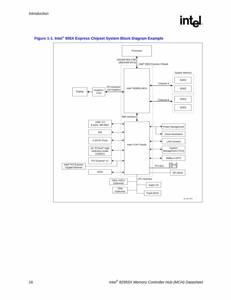
1 Introduction The Intel® 955X Express chipset is designed for use with Intel® Pentium® 4 processor in the 90 nm process in the LGA775 Land Grid Array package, Intel® Pentium® D processor, and Intel® Pentium® processor Extreme Edition based platforms. The chipset contains two components: 82955X Memory Controller Hub (MCH) for the host bridge and I/O Controller Hub 7 (ICH7) for the I/O subsystem. The MCH provides the interface to the processor, main memory, PCI Express*, and the ICH7. The ICH7 is the seventh generation I/O Controller Hub and provides a multitude of I/O related functions. Figure 1-1 shows an example system block diagram for the 955X Express chipset.
This document is the datasheet for the Intel® 82955X MCH. Topics covered include; signal description, system memory map, register descriptions, a description of the MCH interfaces and major functional units, electrical characteristics, ballout definitions, and package characteristics.
Note: Unless otherwise specified, ICH7 refers to the Intel® 82801GB ICH7 and 82801GR ICH7R I/O Controller Hub components.
Introduction
R
16 Intel® 82955X Memory Controller Hub (MCH) Datasheet
Figure 1-1. Intel® 955X Express Chipset System Block Diagram Example
Processor
Intel® 82955X MCH
DDR2
DDR2
DDR2
DDR2
Channel A
200/266 MHz FSB(800/1066 MT/s)
DMI Interface
Sys_Blk_955X
Channel B
GraphicsCard
PCI Express*x16 Graphics
Intel® 955X Express Chipset
System Memory
Display
Intel® ICH7 Family
USB* 2.08 ports, 480 Mb/s
4 SATA* Ports
IDE
Super I/O
Other ASICs(Optional)
PCI Bus
AC '97/Intel® HighDefinition Audio
CODECs
LPC Interface
Power Management
Clock Generation
SystemManagement (TCO)
LAN Connect
SMBus 2.0/I2C
GPIO
PCI Express* x1Intel® PCI ExpressGigabit Ethernet
SPI BIOS
TPM(Optional)
Flash BIOS
Introduction
R
Intel® 82955X Memory Controller Hub (MCH) Datasheet 17
1.1 Terminology Term Description
Accelerated Graphics Port (AGP)
Refers to the AGP/PCI interface that was previously in the MCH components. This port is not on the 82955X MCH; It has been replaced by PCI Express*.
Core The internal base logic in the MCH
CRT Cathode Ray Tube
DED Double-bit Error Detect
DBI Dynamic Bus Inversion
DDR Double Data Rate SDRAM memory technology
DDR2 A second generation Double Data Rate SDRAM memory technology
DMI Direct Media Interface. This is the interface between the MCH and ICH7.
ECC Error Correcting Code
FSB Front Side Bus. This term is synonymous with Host bus or processor bus
Full Reset Full reset is when PWROK is de-asserted. Warm reset is when both RSTIN# and PWROK are asserted.
Host This term is used synonymously with processor.
INTx An interrupt request signal where X stands for interrupts A,B,C, and D
Intel® ICH7 Seventh generation I/O Controller Hub component that contains additional functionality compared to previous ICH components. The I/O Controller Hub component that contains the primary PCI interface, LPC interface, USB2, ATA-100, and other I/O functions. It communicates with the MCH over a proprietary interconnect called DMI.
MCH 82955X Memory Controller Hub component that contains the processor interface, DRAM controller, and x16 PCI Express port (typically the external graphics interface). It communicates with the I/O controller hub (Intel® ICH7*) and other I/O controller hubs over the DMI interconnect.
MSI Message Signaled Interrupt. A transaction initiated outside the host, conveying interrupt information to the receiving agent through the same path that normally carries read and write commands.
PCI Express* Third generation input/output graphics attach called PCI Express Graphics. It is a high-speed serial interface whose configuration is software compatible with the existing PCI specifications. The specific PCI Express implementation intended for connecting the MCH to an external Graphics Controller is a x16 link and replaces AGP.
Primary PCI The physical PCI bus that is driven directly by the ICH7 component. Communication between Primary PCI and the MCH occurs over DMI. Note that the Primary PCI bus is not PCI Bus 0 from a configuration standpoint.
Processor Refers to the Intel® Pentium® 4 processor in the 90 nm process in the LGA775 Land Grid Array package, Intel® Pentium D processor, and Intel® Pentium® processor Extreme Edition.
SCI System Control Interrupt. Used in ACPI protocol.
Introduction
R
18 Intel® 82955X Memory Controller Hub (MCH) Datasheet
Term Description
SEC Single-bit Error Correct
SERR System Error. An indication that an unrecoverable error has occurred on an I/O bus.
SMI System Management Interrupt. SMI is used to indicate any of several system conditions such as thermal sensor events, throttling activated, access to System Management RAM, chassis open, or other system state related activity.
Rank A unit of DRAM corresponding to eight x8 SDRAM devices in parallel or four x16 SDRAM devices in parallel, ignoring ECC. These devices are usually, but not always, mounted on a single side of a DIMM.
TOLM Top Of Low Memory. The highest address below 4 GB for which a processor-initiated memory read or write transaction will create a corresponding cycle to DRAM on the memory interface.
VCO Voltage Controlled Oscillator
1.2 Reference Documents Document Name Doc Number/ Location
Intel® I/O Controller Hub 7 (ICH7) Family Datasheet http://developer.intel.com//design/chipsets/datashts/307013.htm
Intel® 955X Express Chipset Thermal Mechanical Design Guidelines http://developer.intel.com//design/chipsets/designex/307012.htm
Intel® 955X Express Chipset Specification Update http://developer.intel.com//design/chipsets/specupdt/306829.htm
Advanced Configuration and Power Interface Specification, Revision 2.0 http://www.acpi.info/
Advanced Configuration and Power Interface Specification, Revision 1.0b
http://www.acpi.info/
The PCI Local Bus Specification, Revision 2.3 http://www.pcisig.com/specifications
PCI Express* Specification, Revision 1.0a http://www.pcisig.com/specifications
Introduction
R
Intel® 82955X Memory Controller Hub (MCH) Datasheet 19
1.3 MCH Overview The MCH connects to the processor as shown in Figure 1-1. A major role of the MCH in a system is to manage the flow of information between its four interfaces: the processor interface (FSB), the System Memory interface (DRAM controller), the External Graphics interface (PCI Express), and the I/O Controller through DMI interface. This includes arbitrating between the four interfaces when each initiates transactions. The processor interface supports the Pentium 4 processor subset of the Extended Mode of the Scalable Bus Protocol.
The MCH supports one or two channels of DDR2 SDRAM. It also supports PCI Express based external graphics attach. To increase system performance, the MCH incorporates several queues and a write cache. The MCH also contains advanced power management logic.
1.3.1 Host Interface
The MCH is optimized for the Pentium 4 processor in the 90 nm process in the LGA775 Land Grid Array package, Pentium D processor, and Pentium processor Extreme Edition in a LGA775 socket. The MCH supports FSB frequencies of 200 MHz (800 MT/s) and 266 MHz (1066 MT/s) using a scalable FSB Vcc_CPU. The MCH supports the Pentium 4 processor subset of the Extended Mode Scaleable Bus Protocol. The primary enhancements over the Compatible Mode P6 bus protocol are source synchronous double-pumped (2x) address and source synchronous quad-pumped (4x) data. Other MCH supported features of the host interface include: Hyper-Threading Technology (HT Technology), Pentium 4 processor FSB interrupt delivery, FSB Dynamic Bus Inversion (DBI), 12-deep in-order queue, and a 1-deep defer queue.
The MCH supports 36-bit host addressing, decoding up to 8 GB of the processor’s usable memory address space. Host-initiated I/O cycles are decoded to PCI Express, DMI, or the MCH configuration space. Host-initiated memory cycles are decoded to PCI Express, DMI or main memory. PCI Express device accesses to non-cacheable system memory are not snooped on the host bus. Memory accesses initiated from PCI Express using PCI semantics and from DMI to system SDRAM will be snooped on the host bus.
Introduction
R
20 Intel® 82955X Memory Controller Hub (MCH) Datasheet
1.3.2 System Memory Interface The MCH integrates a system memory DDR2 controller with two, 64-bit wide interfaces. Only Double Data Rate (DDR2) memory is supported; consequently, the buffers support only SSTL_1.8 V signal interfaces. The memory controller interface is fully configurable through a set of control registers. Features of the MCH memory controller include:
• Maximum memory size is 8 GB.
• Directly supports one or two channels of memory (each channel consisting of 64 data lines) ⎯ The memory channels are asymmetric: "Stacked" channels are assigned addresses
serially. Channel B addresses are assigned after all Channel A addresses. ⎯ The memory channels are interleaved: Addresses are ping-ponged between the channels
after each cache line (64-B boundary).
• Available bandwidth up to 5.3 GB/s (DDR2 667) for single-channel mode or dual-channel asymmetric mode and 10.7 GB/s (DDR2 667) in dual-channel Interleaved mode.
• Supports standard ECC (Error Correcting Code) x8 only or Non-ECC x8 and x16 DIMMs.
• Supports DDR2 memory DIMM frequencies of 533 and 667 MHz. The speed used in all channels is the speed of the slowest DIMM in the system.
• Supports 256-Mb, 512-Mb and 1-Gb DDR2 technologies for x8 and x16 devices.
• Supports four banks for all DDR2 devices up to 512-Mbit density. Supports eight banks for 1-Gbit DDR2 devices.
• DDR2-667 1Gbit technology or DDR2-667 4-4-4 are Not supported
• Supports only unbuffered DIMMs.
• Supports opportunistic refresh.
• In dual channel mode the MCH supports 32 simultaneously open pages.
• SPD (Serial Presence Detect) scheme for DIMM detection support.
• Suspend-to-RAM support using CKE.
• Supports configurations defined in the JEDEC DDR2 DIMM specification only.
• Directly supports two channels of ECC or non-ECC DDR2 DIMMs.
• Supports Partial Writes to memory using Data Mask (DM) signals, only when not using ECC.
• Supports a burst length of 8 for single-channel and dual-channel interleaved and asymmetric operating modes.
• Supports Enhanced Memory Interleave.

Introduction
R
Intel® 82955X Memory Controller Hub (MCH) Datasheet 21
1.3.3 PCI Express* Graphics Interface
The PCI Express interface supports 16 bi-directional lanes used for next generation graphics attach. Each PCI Express graphic lane supports a bi-directional transfer rate of 2.5 Gb/s for a theoretical bandwidth of 8 GBs when in x16 mode. Features of the PCI Express interface include:
• One 16-lane PCI Express port intended for graphics attach, compatible to the PCI Express* Base Specification, Revision 1.0a.
• A base PCI Express frequency of 2.5 Gb/s only.
• Raw bit-rate on the data pins of 2.5 Gb/s, resulting in a real bandwidth per pair of 250 MB/s given the 8b/10b encoding used to transmit data across this interface.
• Maximum theoretical realized bandwidth on the interface of 4 GB/s in each direction simultaneously, for an aggregate of 8 GB/s when x16.
• PCI Express extended configuration space. The first 256 bytes of configuration space alias directly to the PCI compatibility configuration space. The remaining portion of the fixed 4-KB block of memory-mapped space above that (starting at 100h) is known as extended configuration space.
• PCI Express enhanced addressing mechanism. Accessing the device configuration space in a flat memory mapped fashion.
• Automatic discovery, negotiation, and training of link out of reset.
• Supports traditional PCI style traffic (asynchronous snooped, PCI ordering).
• Supports traditional AGP style traffic (asynchronous non-snooped, PCI Express-relaxed ordering).
• Hierarchical PCI-compliant configuration mechanism for downstream devices (i.e., normal PCI 2.3 configuration space as a PCI-to-PCI bridge).
• Supports “static” lane numbering reversal. This method of lane reversal is controlled by a Hardware Reset strap, and reverses both the receivers and transmitters for all lanes (e.g., TX15->TX0, RX15->RX0). This method is transparent to all external devices and is different than lane reversal as defined in the PCI Express specification. In particular, link initialization is not affected by static lane reversal.
Introduction
R
22 Intel® 82955X Memory Controller Hub (MCH) Datasheet
1.3.4 Direct Media Interface (DMI)
Direct Media Interface (DMI) is the chip-to-chip connection between the MCH and ICH7. This high-speed interface integrates advanced priority-based servicing allowing for concurrent traffic and true isochronous transfer capabilities. Base functionality is completely software transparent permitting current and legacy software to operate normally.
To provide for true isochronous transfers and configurable Quality of Service (QoS) transactions, the ICH7 supports two virtual channels on DMI: VC0 and VC1. These two channels provide a fixed arbitration scheme where VC1 is always the highest priority. VC0 is the default conduit of traffic for DMI and is always enabled. VC1 must be specifically enabled and configured at both ends of the DMI link (i.e., the Intel ICH7 and MCH). Configuration registers for DMI, virtual channel support, and DMI active state power management (ASPM) are in the RCRB space in the MCH Register Description. Features of the DMI include:
• A chip-to-chip connection interface to Intel ICH7.
• 2 GB/s point-to-point DMI to ICH7 (1 GB/s each direction).
• 100 MHz reference clock (shared with PCI Express graphics attach).
• 32-bit downstream addressing.
• APIC and MSI interrupt messaging support. MCH will send Intel-defined “End Of Interrupt” broadcast message when initiated by the processor.
• Message Signaled Interrupt (MSI) messages.
• SMI, SCI, and SERR error indication.
• Legacy support for ISA regime protocol (PHOLD/PHOLDA) required for parallel port DMA, floppy drive, and LPC bus masters.
1.3.5 System Interrupts • Supports both 8259 and Pentium 4 processor FSB interrupt delivery mechanisms.
• Supports interrupts signaled as upstream memory writes from PCI Express and DMI. ⎯ MSIs routed directly to FSB. ⎯ From I/OxAPICs.
• Provides redirection for IPI (Inter-Processor Interrupts) and upstream interrupts to the FSB.
Introduction
R
Intel® 82955X Memory Controller Hub (MCH) Datasheet 23
1.3.6 MCH Clocking
The Differential FSB clock of 200/266 MHz (HCLKP/HCLKN) supports transfer rates of 800/1066 MT/s. The Host PLL generates 2X, 4X, and 8X versions of the host clock for internal optimizations. The MCH core clock is synchronized to the host clock.
The internal and external memory clocks of 266 MHz and 333 MHz are generated from one of two MCH PLLs that use the Host clock as a reference. Also included are 2x and 4x clocks for internal optimizations.
The PCI Express core clock of 250 MHz is generated from a separate PCI Express PLL. This clock uses the fixed 100 MHz serial reference clock (GCLKP/GCLKN) for reference.
All of the above mentioned clocks are capable of tolerating Spread Spectrum clocking as defined in the Clock Generator specification. Host, Memory, and PCI Express PLLs, and all associated internal clocks are disabled until PWROK is asserted.
1.3.7 Power Management
The MCH power management support includes:
• PC99 suspend to DRAM support (“STR”, mapped to ACPI state S3)
• SMRAM space remapping to A0000h (128 KB)
• Supports extended SMRAM space above 256 MB, additional 1-MB TSEG from the Top of Low Usable DRAM (TOLUD), and cacheable (cacheablility controlled by the processor)
• ACPI Revision 1.0 compatible power management
• Supports processor states: C0 and C1
• Supports system states: S0, S1D, S3, S4, and S5
• Supports processor Thermal Management 2 (TM2)
• Microsoft Windows NT* Hardware Design Guide v1.0 compliant
§

Introduction
R
24 Intel® 82955X Memory Controller Hub (MCH) Datasheet
Signal Description
R
Intel® 82955X Memory Controller Hub (MCH) Datasheet 25
2 Signal Description This section provides a detailed description of MCH signals. The signals are arranged in functional groups according to their associated interface.
The following notations are used to describe the signal type:
PCIE PCI Express interface signals. These signals are compatible with PCI Express 1.0 Signaling Environment AC Specifications and are AC coupled. The buffers are not 3.3 V tolerant. Differential voltage spec = (|D+ – D-|) * 2 = 1.2 Vmax. Single-ended maximum = 1.5 V. Single-ended minimum = 0 V.
DMI Direct Media Interface signals. These signals are compatible with PCI Express 1.0 Signaling Environment AC Specifications, but are DC coupled. The buffers are not 3.3 V tolerant. Differential voltage spec = (|D+ – D-|) * 2 = 1.2 Vmax. Single-ended maximum = 1.5 V. Single-ended minimum = 0 V.
CMOS CMOS buffers. 1.5 V tolerant.
COD CMOS Open Drain buffers. 2.5 V tolerant.
HCSL Host Clock Signal Level buffers. Current mode differential pair. Differential typical swing = (|D+ - D-|) * 2 = 1.4 V. Single ended input tolerant from -0.35 V to 1.2 V. Typical crossing voltage 0.35 V.
HVCMOS High Voltage CMOS buffers. 2.5 V tolerant.
HVIN High Voltage CMOS input-only buffers. 3.3 V tolerant.
SSTL-1.8 Stub Series Termination Logic. These are 1.8 V output capable buffers. 1.8 V tolerant.
A Analog reference or output. These signals may be used as a threshold voltage or for buffer compensation.
Signal Description
R
26 Intel® 82955X Memory Controller Hub (MCH) Datasheet
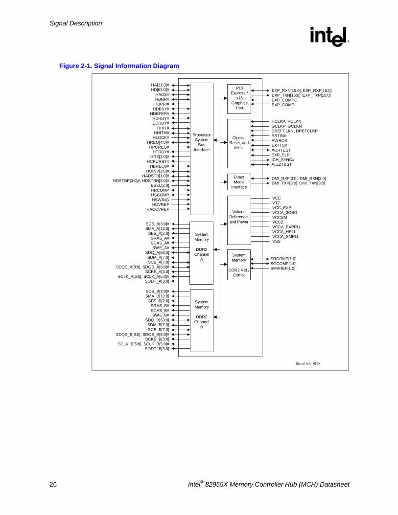
Figure 2-1. Signal Information Diagram
Signal_Info_955X
SCS_A[3:0]#SMA_A[13:0]
SBS_A[2:0]SRAS_A#SCAS_A#SWE_A#
SDQ_A[63:0]SDM_A[7:0]SCB_A[7:0]
SDQS_A[8:0], SDQS_A[8:0]#SCKE_A[3:0]
SCLK_A[5:0], SCLK_A[5:0]#SODT_A[3:0]
ProcessorSystem
BusInterface
HA[31:3]#HD[63:0]#
HADS#HBNR#HBPRI#
HDBSY#HDEFER#
HDRDY#HEDRDY#
HHIT#HHITM#HLOCK#
HREQ[4:0]#HPCREQ#
HTRDY#HRS[2:0]#
HCPURST#HBREQ0#
HDINV[3:0]#HADSTB[1:0]#
HDSTBP[3:0]#, HDSTBN[3:0]#BSEL[2:0]HRCOMPHSCOMPHSWINGHDVREF
HACCVREF
SystemMemory
DDR2Channel
A
VCCVTTVCC_EXPVCCA_3GBGVCCSMVCC2VCCA_EXPPLLVCCA_HPLLVCCA_SMPLLVSS
VoltageReference,and Power
PCIExpress *
x16Graphics
Port
EXP_RXN[15:0], EXP_RXP[15:0]EXP_TXN[15:0], EXP_TXP[15:0]EXP_COMPOEXP_COMPI
SCS_B[3:0]#SMA_B[13:0]
SBS_B[2:0]SRAS_B#SCAS_B#SWE_B#
SDQ_B[63:0]SDM_B[7:0]SCB_B[7:0]
SDQS_B[8:0], SDQS_B[8:0]#SCKE_B[3:0]
SCLK_B[5:0], SCLK_B[5:0]#SODT_B[3:0]
SystemMemory
DDR2Channel
B
HCLKP, HCLKNGCLKP, GCLKNDREFCLKN, DREFCLKPRSTIN#PWROKEXTTS#XORTESTEXP_SLRICH_SYNC#ALLZTEST
Clocks,Reset, and
Misc.
DirectMedia
Interface
DMI_RXP[3:0], DMI_RXN[3:0]DMI_TXP[3:0], DMI_TXN[3:0]
SRCOMP[1:0]SOCOMP[1:0]SMVREF[1:0]
SystemMemory
DDR2 Ref./Comp.
Signal Description
R
Intel® 82955X Memory Controller Hub (MCH) Datasheet 27
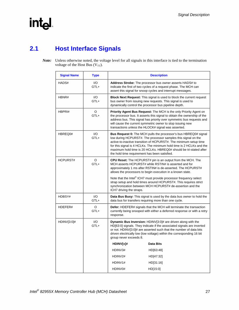
2.1 Host Interface Signals
Note: Unless otherwise noted, the voltage level for all signals in this interface is tied to the termination voltage of the Host Bus (VTT).
Signal Name Type Description
HADS# I/O GTL+
Address Strobe: The processor bus owner asserts HADS# to indicate the first of two cycles of a request phase. The MCH can assert this signal for snoop cycles and interrupt messages.
HBNR# I/O GTL+
Block Next Request: This signal is used to block the current request bus owner from issuing new requests. This signal is used to dynamically control the processor bus pipeline depth.
HBPRI# O GTL+
Priority Agent Bus Request: The MCH is the only Priority Agent on the processor bus. It asserts this signal to obtain the ownership of the address bus. This signal has priority over symmetric bus requests and will cause the current symmetric owner to stop issuing new transactions unless the HLOCK# signal was asserted.
HBREQ0# I/O GTL+
Bus Request 0: The MCH pulls the processor’s bus HBREQ0# signal low during HCPURST#. The processor samples this signal on the active-to-inactive transition of HCPURST#. The minimum setup time for this signal is 4 HCLKs. The minimum hold time is 2 HCLKs and the maximum hold time is 20 HCLKs. HBREQ0# should be tri-stated after the hold time requirement has been satisfied.
HCPURST# O GTL+
CPU Reset: The HCPURST# pin is an output from the MCH. The MCH asserts HCPURST# while RSTIN# is asserted and for approximately 1 ms after RSTIN# is de-asserted. The HCPURST# allows the processors to begin execution in a known state.
Note that the Intel® ICH7 must provide processor frequency select strap setup and hold times around HCPURST#. This requires strict synchronization between MCH HCPURST# de-assertion and the ICH7 driving the straps.
HDBSY# I/O GTL+
Data Bus Busy: This signal is used by the data bus owner to hold the data bus for transfers requiring more than one cycle.
HDEFER# O GTL+
Defer: HDEFER# signals that the MCH will terminate the transaction currently being snooped with either a deferred response or with a retry response.
HDINV[3:0]# I/O GTL+
Dynamic Bus Inversion: HDINV[3:0]# are driven along with the HD[63:0] signals. They indicate if the associated signals are inverted or not. HDINV[3:0]# are asserted such that the number of data bits driven electrically low (low voltage) within the corresponding 16 bit group never exceeds 8.
HDINV[x]# Data Bits
HDINV3# HD[63:48]
HDINV2# HD[47:32]
HDINV1# HD[31:16]
HDINV0# HD[15:0]
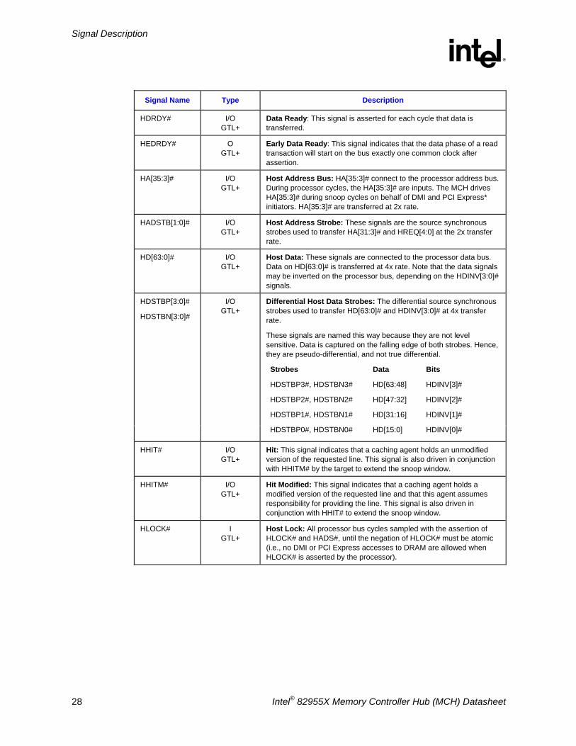
Signal Description
R
28 Intel® 82955X Memory Controller Hub (MCH) Datasheet
Signal Name Type Description
HDRDY# I/O GTL+
Data Ready: This signal is asserted for each cycle that data is transferred.
HEDRDY# O GTL+
Early Data Ready: This signal indicates that the data phase of a read transaction will start on the bus exactly one common clock after assertion.
HA[35:3]# I/O GTL+
Host Address Bus: HA[35:3]# connect to the processor address bus. During processor cycles, the HA[35:3]# are inputs. The MCH drives HA[35:3]# during snoop cycles on behalf of DMI and PCI Express* initiators. HA[35:3]# are transferred at 2x rate.
HADSTB[1:0]# I/O GTL+
Host Address Strobe: These signals are the source synchronous strobes used to transfer HA[31:3]# and HREQ[4:0] at the 2x transfer rate.
HD[63:0]# I/O GTL+
Host Data: These signals are connected to the processor data bus. Data on HD[63:0]# is transferred at 4x rate. Note that the data signals may be inverted on the processor bus, depending on the HDINV[3:0]# signals.
HDSTBP[3:0]#
HDSTBN[3:0]#
I/O GTL+
Differential Host Data Strobes: The differential source synchronous strobes used to transfer HD[63:0]# and HDINV[3:0]# at 4x transfer rate.
These signals are named this way because they are not level sensitive. Data is captured on the falling edge of both strobes. Hence, they are pseudo-differential, and not true differential.
Strobes Data Bits
HDSTBP3#, HDSTBN3# HD[63:48] HDINV[3]#
HDSTBP2#, HDSTBN2# HD[47:32] HDINV[2]#
HDSTBP1#, HDSTBN1# HD[31:16] HDINV[1]#
HDSTBP0#, HDSTBN0# HD[15:0] HDINV[0]#
HHIT# I/O GTL+
Hit: This signal indicates that a caching agent holds an unmodified version of the requested line. This signal is also driven in conjunction with HHITM# by the target to extend the snoop window.
HHITM# I/O GTL+
Hit Modified: This signal indicates that a caching agent holds a modified version of the requested line and that this agent assumes responsibility for providing the line. This signal is also driven in conjunction with HHIT# to extend the snoop window.
HLOCK# I GTL+
Host Lock: All processor bus cycles sampled with the assertion of HLOCK# and HADS#, until the negation of HLOCK# must be atomic (i.e., no DMI or PCI Express accesses to DRAM are allowed when HLOCK# is asserted by the processor).
Signal Description
R
Intel® 82955X Memory Controller Hub (MCH) Datasheet 29
Signal Name Type Description
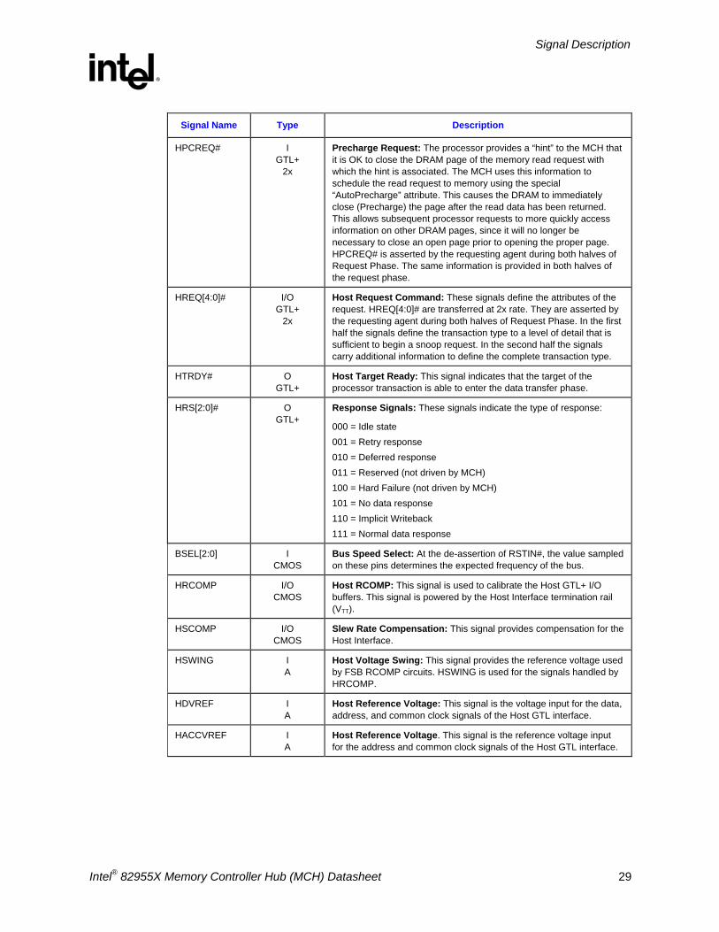
HPCREQ# I GTL+
2x
Precharge Request: The processor provides a “hint” to the MCH that it is OK to close the DRAM page of the memory read request with which the hint is associated. The MCH uses this information to schedule the read request to memory using the special “AutoPrecharge” attribute. This causes the DRAM to immediately close (Precharge) the page after the read data has been returned. This allows subsequent processor requests to more quickly access information on other DRAM pages, since it will no longer be necessary to close an open page prior to opening the proper page. HPCREQ# is asserted by the requesting agent during both halves of Request Phase. The same information is provided in both halves of the request phase.
HREQ[4:0]# I/O GTL+
2x
Host Request Command: These signals define the attributes of the request. HREQ[4:0]# are transferred at 2x rate. They are asserted by the requesting agent during both halves of Request Phase. In the first half the signals define the transaction type to a level of detail that is sufficient to begin a snoop request. In the second half the signals carry additional information to define the complete transaction type.
HTRDY# O GTL+
Host Target Ready: This signal indicates that the target of the processor transaction is able to enter the data transfer phase.
HRS[2:0]# O GTL+
Response Signals: These signals indicate the type of response:
000 = Idle state 001 = Retry response 010 = Deferred response 011 = Reserved (not driven by MCH) 100 = Hard Failure (not driven by MCH) 101 = No data response 110 = Implicit Writeback 111 = Normal data response
BSEL[2:0] I CMOS
Bus Speed Select: At the de-assertion of RSTIN#, the value sampled on these pins determines the expected frequency of the bus.
HRCOMP I/O CMOS
Host RCOMP: This signal is used to calibrate the Host GTL+ I/O buffers. This signal is powered by the Host Interface termination rail (VTT).
HSCOMP I/O CMOS
Slew Rate Compensation: This signal provides compensation for the Host Interface.
HSWING I A
Host Voltage Swing: This signal provides the reference voltage used by FSB RCOMP circuits. HSWING is used for the signals handled by HRCOMP.
HDVREF I A
Host Reference Voltage: This signal is the voltage input for the data, address, and common clock signals of the Host GTL interface.
HACCVREF I A
Host Reference Voltage. This signal is the reference voltage input for the address and common clock signals of the Host GTL interface.
Signal Description
R
30 Intel® 82955X Memory Controller Hub (MCH) Datasheet
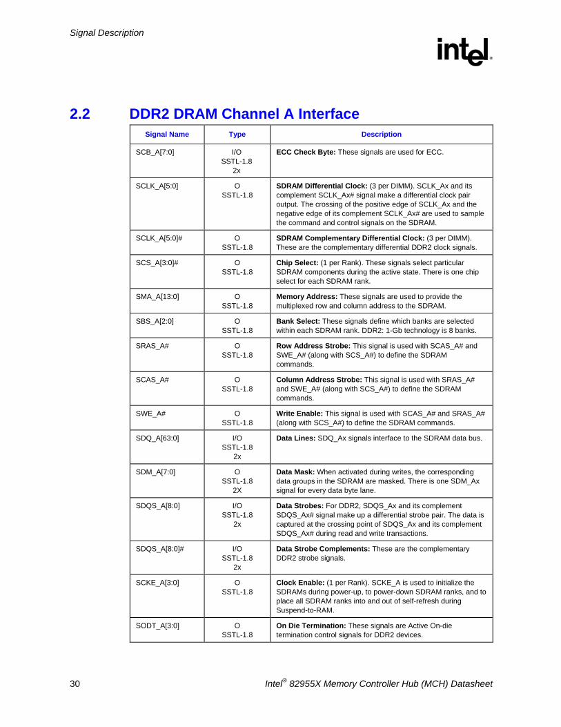
2.2 DDR2 DRAM Channel A Interface Signal Name Type Description
SCB_A[7:0] I/O SSTL-1.8
2x
ECC Check Byte: These signals are used for ECC.
SCLK_A[5:0] O SSTL-1.8
SDRAM Differential Clock: (3 per DIMM). SCLK_Ax and its complement SCLK_Ax# signal make a differential clock pair output. The crossing of the positive edge of SCLK_Ax and the negative edge of its complement SCLK_Ax# are used to sample the command and control signals on the SDRAM.
SCLK_A[5:0]# O SSTL-1.8
SDRAM Complementary Differential Clock: (3 per DIMM). These are the complementary differential DDR2 clock signals.
SCS_A[3:0]# O SSTL-1.8
Chip Select: (1 per Rank). These signals select particular SDRAM components during the active state. There is one chip select for each SDRAM rank.
SMA_A[13:0] O SSTL-1.8
Memory Address: These signals are used to provide the multiplexed row and column address to the SDRAM.
SBS_A[2:0] O SSTL-1.8
Bank Select: These signals define which banks are selected within each SDRAM rank. DDR2: 1-Gb technology is 8 banks.
SRAS_A# O SSTL-1.8
Row Address Strobe: This signal is used with SCAS_A# and SWE_A# (along with SCS_A#) to define the SDRAM commands.
SCAS_A# O SSTL-1.8
Column Address Strobe: This signal is used with SRAS_A# and SWE_A# (along with SCS_A#) to define the SDRAM commands.
SWE_A# O SSTL-1.8
Write Enable: This signal is used with SCAS_A# and SRAS_A# (along with SCS_A#) to define the SDRAM commands.
SDQ_A[63:0] I/O SSTL-1.8
2x
Data Lines: SDQ_Ax signals interface to the SDRAM data bus.
SDM_A[7:0] O SSTL-1.8
2X
Data Mask: When activated during writes, the corresponding data groups in the SDRAM are masked. There is one SDM_Ax signal for every data byte lane.
SDQS_A[8:0] I/O SSTL-1.8
2x
Data Strobes: For DDR2, SDQS_Ax and its complement SDQS_Ax# signal make up a differential strobe pair. The data is captured at the crossing point of SDQS_Ax and its complement SDQS_Ax# during read and write transactions.
SDQS_A[8:0]# I/O SSTL-1.8
2x
Data Strobe Complements: These are the complementary DDR2 strobe signals.
SCKE_A[3:0] O SSTL-1.8
Clock Enable: (1 per Rank). SCKE_A is used to initialize the SDRAMs during power-up, to power-down SDRAM ranks, and to place all SDRAM ranks into and out of self-refresh during Suspend-to-RAM.
SODT_A[3:0] O SSTL-1.8
On Die Termination: These signals are Active On-die termination control signals for DDR2 devices.
Signal Description
R
Intel® 82955X Memory Controller Hub (MCH) Datasheet 31
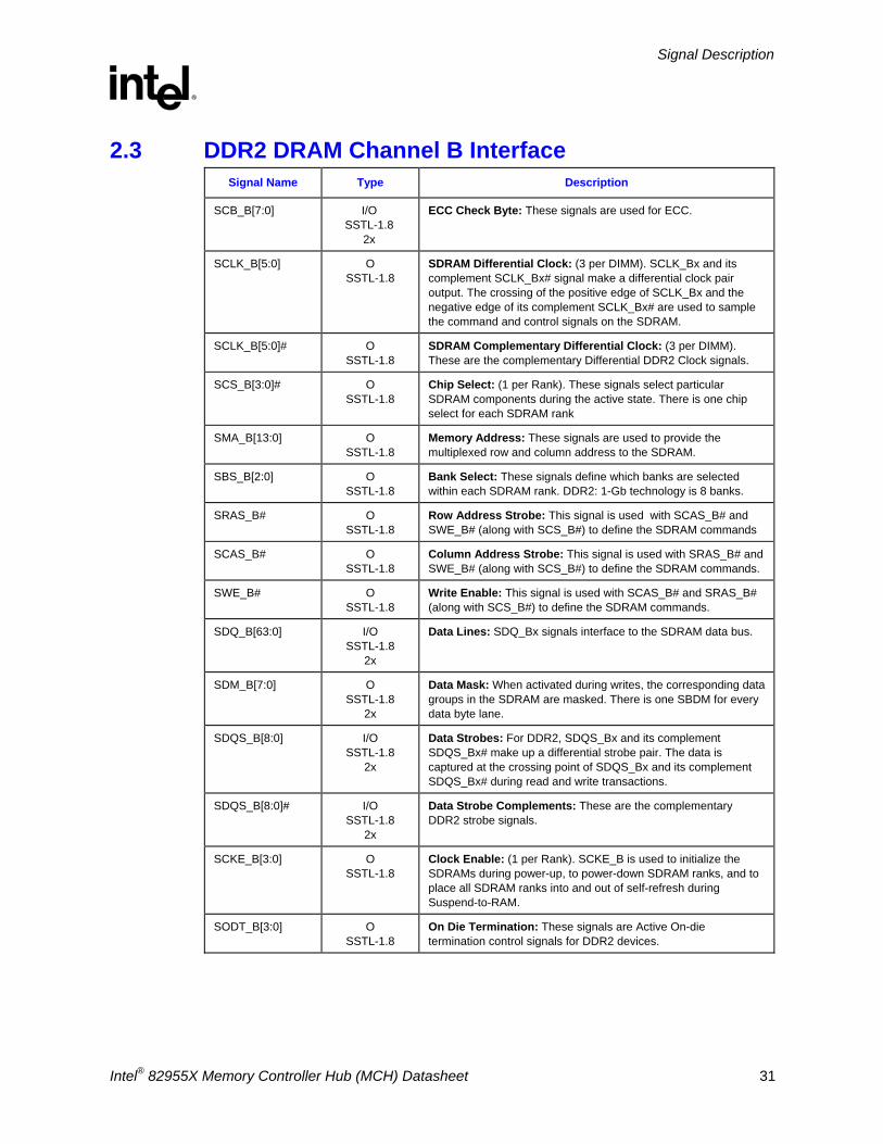
2.3 DDR2 DRAM Channel B Interface Signal Name Type Description
SCB_B[7:0] I/O SSTL-1.8
2x
ECC Check Byte: These signals are used for ECC.
SCLK_B[5:0] O SSTL-1.8
SDRAM Differential Clock: (3 per DIMM). SCLK_Bx and its complement SCLK_Bx# signal make a differential clock pair output. The crossing of the positive edge of SCLK_Bx and the negative edge of its complement SCLK_Bx# are used to sample the command and control signals on the SDRAM.
SCLK_B[5:0]# O SSTL-1.8
SDRAM Complementary Differential Clock: (3 per DIMM). These are the complementary Differential DDR2 Clock signals.
SCS_B[3:0]# O SSTL-1.8
Chip Select: (1 per Rank). These signals select particular SDRAM components during the active state. There is one chip select for each SDRAM rank
SMA_B[13:0] O SSTL-1.8
Memory Address: These signals are used to provide the multiplexed row and column address to the SDRAM.
SBS_B[2:0] O SSTL-1.8
Bank Select: These signals define which banks are selected within each SDRAM rank. DDR2: 1-Gb technology is 8 banks.
SRAS_B# O SSTL-1.8
Row Address Strobe: This signal is used with SCAS_B# and SWE_B# (along with SCS_B#) to define the SDRAM commands
SCAS_B# O SSTL-1.8
Column Address Strobe: This signal is used with SRAS_B# and SWE_B# (along with SCS_B#) to define the SDRAM commands.
SWE_B# O SSTL-1.8
Write Enable: This signal is used with SCAS_B# and SRAS_B# (along with SCS_B#) to define the SDRAM commands.
SDQ_B[63:0] I/O SSTL-1.8
2x
Data Lines: SDQ_Bx signals interface to the SDRAM data bus.
SDM_B[7:0] O SSTL-1.8
2x
Data Mask: When activated during writes, the corresponding data groups in the SDRAM are masked. There is one SBDM for every data byte lane.
SDQS_B[8:0] I/O SSTL-1.8
2x
Data Strobes: For DDR2, SDQS_Bx and its complement SDQS_Bx# make up a differential strobe pair. The data is captured at the crossing point of SDQS_Bx and its complement SDQS_Bx# during read and write transactions.
SDQS_B[8:0]# I/O SSTL-1.8
2x
Data Strobe Complements: These are the complementary DDR2 strobe signals.
SCKE_B[3:0] O SSTL-1.8
Clock Enable: (1 per Rank). SCKE_B is used to initialize the SDRAMs during power-up, to power-down SDRAM ranks, and to place all SDRAM ranks into and out of self-refresh during Suspend-to-RAM.
SODT_B[3:0] O SSTL-1.8
On Die Termination: These signals are Active On-die termination control signals for DDR2 devices.
Signal Description
R
32 Intel® 82955X Memory Controller Hub (MCH) Datasheet
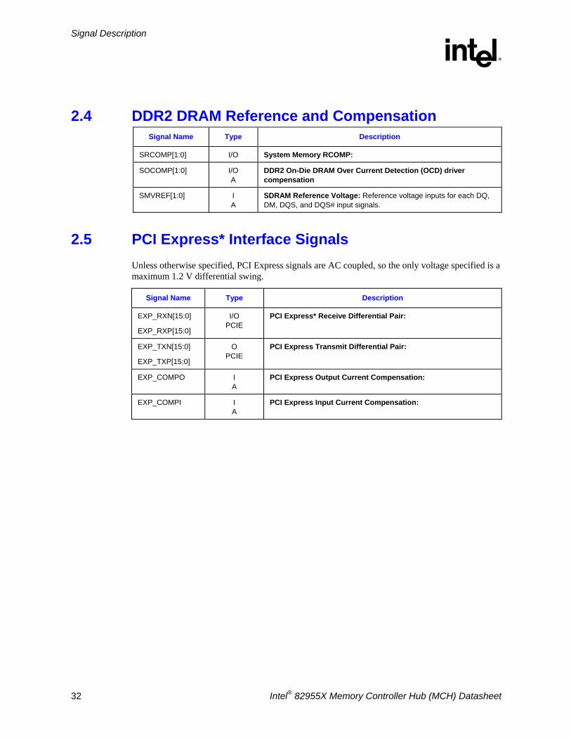
2.4 DDR2 DRAM Reference and Compensation Signal Name Type Description
SRCOMP[1:0] I/O System Memory RCOMP:
SOCOMP[1:0] I/O A
DDR2 On-Die DRAM Over Current Detection (OCD) driver compensation
SMVREF[1:0] I A
SDRAM Reference Voltage: Reference voltage inputs for each DQ, DM, DQS, and DQS# input signals.
2.5 PCI Express* Interface Signals Unless otherwise specified, PCI Express signals are AC coupled, so the only voltage specified is a maximum 1.2 V differential swing.
Signal Name Type Description
EXP_RXN[15:0]
EXP_RXP[15:0]
I/O PCIE
PCI Express* Receive Differential Pair:
EXP_TXN[15:0]
EXP_TXP[15:0]
O PCIE
PCI Express Transmit Differential Pair:
EXP_COMPO I A
PCI Express Output Current Compensation:
EXP_COMPI I A
PCI Express Input Current Compensation:
Signal Description
R
Intel® 82955X Memory Controller Hub (MCH) Datasheet 33
2.6 Clocks, Reset, and Miscellaneous Signal Name Type Description
HCLKP
HCLKN
I HCSL
Differential Host Clock In: These pins receive a differential host clock from the external clock synthesizer. This clock is used by all of the MCH logic that is in the Host clock domain. Memory domain clocks are also derived from this source.
GCLKP
GCLKN
I HCSL
Differential PCI Express* Clock In: These pins receive a differential 100 MHz serial reference clock from the external clock synthesizer. This clock is used to generate the clocks necessary for the support of PCI Express.
RSTIN# I HVIN
Reset In: When asserted, this signal will asynchronously reset the MCH logic. This signal is connected to the PCIRST# output of the Intel® ICH7. All PCI Express graphics attach output signals will also tri-state compliant to PCI Express* Base Specification , Revision 1.0a.
This input should have a Schmitt trigger to avoid spurious resets. This signal is required to be 3.3 V tolerant.
PWROK I HVIN
Power OK: When asserted, PWROK is an indication to the MCH that core power has been stable for at least 10 us.
EXTTS# I HVCMOS
External Thermal Sensor Input: This signal may connect to a precision thermal sensor located on or near the DIMMs. If the system temperature reaches a dangerously high value, then this signal can be used to trigger the start of system thermal management. This signal is activated when an increase in temperature causes a voltage to cross some threshold in the sensor.
EXP_SLR I CMOS
PCI Express* Static Lane Reversal: MCH’s PCI Express lane numbers are reversed.
0 = MCH’s PCI Express lane numbers are reversed 1 = Normal operation
ICH_SYNC# O HVCMOS
ICH Sync: This signal is connected to the MCH_SYNCH# signal on the ICH7.
XORTEST I/O GTL+
XOR Test: This signal is used for Bed of Nails testing by OEMs to execute XOR Chain test.
ALLZTEST I/O GTL+
All Z Test: As an input this signal is used for Bed of Nails testing by OEMs to execute XOR Chain test. It is used as an output for XOR chain testing.
2.7 Direct Media Interface (DMI) EDS Signal Name Type Description
DMI_RXP[3:0]
DMI_RXN[3:0]
I/O DMI
Direct Media Interface: Receive differential pair (Rx)
DMI_TXP[3:0]
DMI_TXN[3:0]
O DMI
Direct Media Interface: Transmit differential pair (Tx)
Signal Description
R
34 Intel® 82955X Memory Controller Hub (MCH) Datasheet
2.8 Power, Ground Name Voltage Description
VCC 1.5 V Core Power
VTT 1.2 V Processor System Bus Power
VCC_EXP 1.5 V PCI Express* and DMI Power
VCCA_3GBG 2.5 V PCI Express and DMI Analog Bandgap
VCCSM 1.8 V System Memory Power
VCC2 2.5 V 2.5 V CMOS Power
VCCA_EXPPLL 1.5 V PCI Express PLL Analog Power
VCCA_HPLL 1.5 V Host PLL Analog Power
VCCA_SMPLL 1.5 V System Memory PLL Analog Power
VSS 0 V Ground
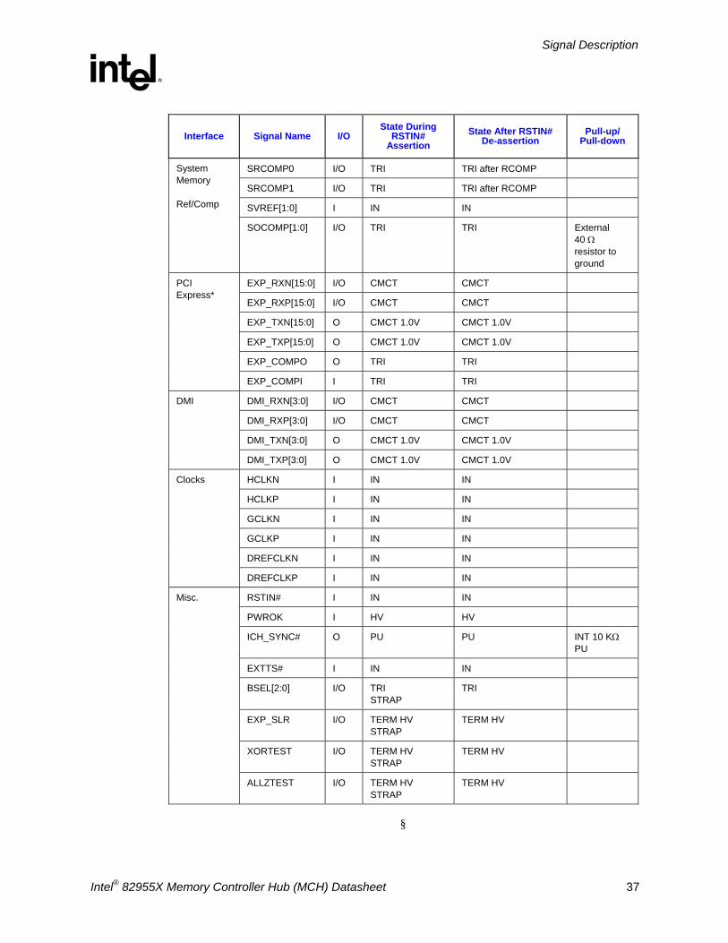
2.9 Reset States and Pull-up/Pull-downs This section describes the expected states of the MCH I/O buffers during and immediately after the assertion of RSTIN#. This table only refers to the contributions on the interface from the MCH and does NOT reflect any external influence (such as external pull-up/pull-down resistors or external drivers).
Legend:
DRIVE: Strong drive (to normal value supplied by core logic if not otherwise stated) .
TERM: Normal termination devices are turned on.
LV: Low voltage.
HV: High voltage.
IN: Input buffer enabled.
TRI: Tri-state.
PU: Weak internal pull-up: 7.2 KΩ – 11.1 KΩ, unless otherwise specified.
PD: Weak internal pull-down: 600 Ω – 880 Ω unless otherwise specified.
CMCT: Common Mode Center Tapped. Differential signals are weakly driven to the common mode central voltage.
STRAP: Strap input sampled on the asserting edge of PWROK.
Signal Description
R
Intel® 82955X Memory Controller Hub (MCH) Datasheet 35
Interface Signal Name I/O State During
RSTIN# Assertion
State After RSTIN# De-assertion
Pull-up/ Pull-down
HCPURST# O DRIVE LV TERM HV after approximately 1ms
HADSTB[1:0]# I/O TERM HV TERM HV
HA[35:3]# I/O TERM HV STRAP
POC
HD[63:0] I/O TERM HV TERM HV
HDSTBP[3:0]# I/O TERM HV TERM HV
HDSTBN[3:0]# I/O TERM HV TERM HV
HDINV[3:0]# I/O TERM HV TERM HV
HADS# I/O TERM HV TERM HV
HBNR# I/O TERM HV TERM HV
HBPRI# O TERM HV TERM HV
HDBSY# I/O TERM HV TERM HV
HDEFER# O TERM HV TERM HV
HDRDY# I/O TERM HV TERM HV
HEDRDY# O TERM HV TERM HV
HHIT# I/O TERM HV TERM HV
HHITM# I/O TERM HV TERM HV
HLOCK# I/O TERM HV TERM HV
HREQ[4:0]# I/O TERM HV TERM HV
HTRDY# O TERM HV TERM HV
HRS[2:0]# I TERM HV TERM HV
HBREQ0# O TERM HV TERM HV
HPCREQ# I TERM HV TERM HV
HDREF I IN IN
HRCOMP I/O TRI TRI after RCOMP RCOMP
HSWING I IN IN
HSCOMP I/O TRI TRI
Host I/F
HACCVREF I IN IN
Signal Description
R
36 Intel® 82955X Memory Controller Hub (MCH) Datasheet
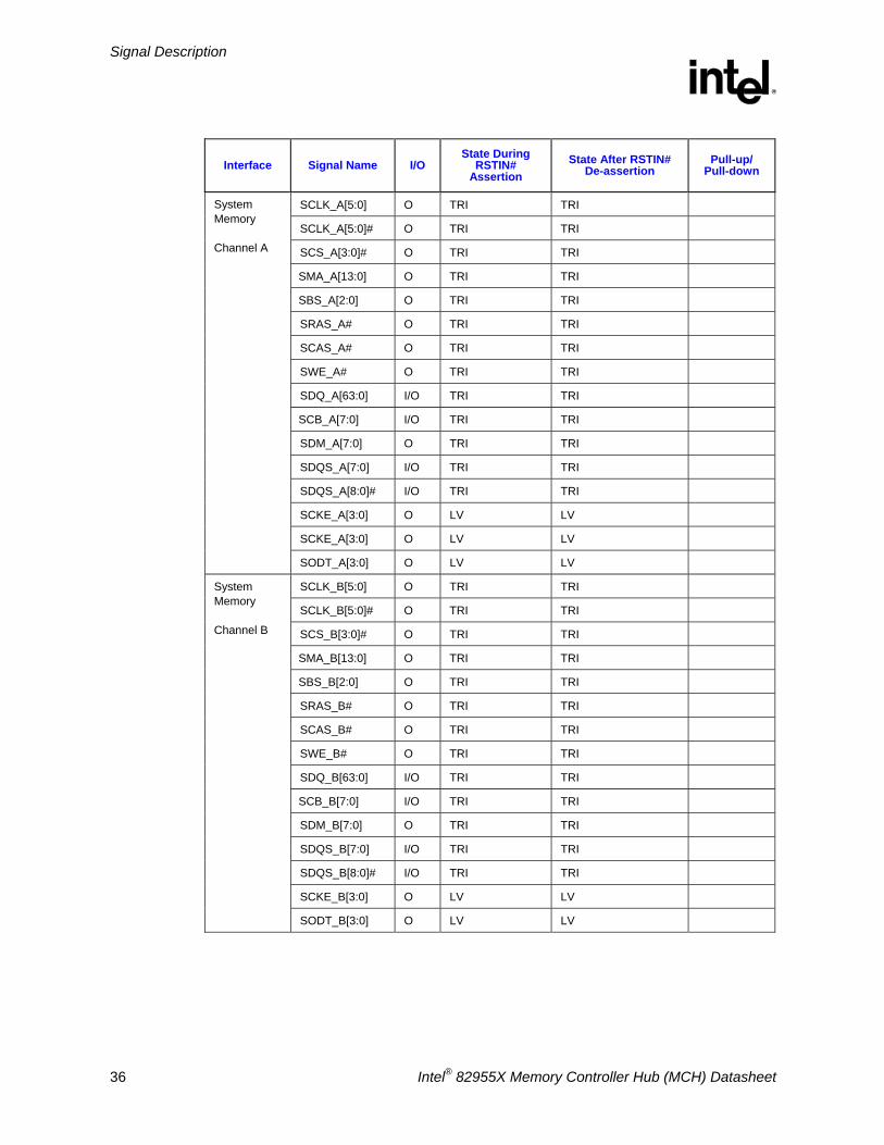
Interface Signal Name I/O State During
RSTIN# Assertion
State After RSTIN# De-assertion
Pull-up/ Pull-down
SCLK_A[5:0] O TRI TRI
SCLK_A[5:0]# O TRI TRI
SCS_A[3:0]# O TRI TRI
SMA_A[13:0] O TRI TRI
SBS_A[2:0] O TRI TRI
SRAS_A# O TRI TRI
SCAS_A# O TRI TRI
SWE_A# O TRI TRI
SDQ_A[63:0] I/O TRI TRI
SCB_A[7:0] I/O TRI TRI
SDM_A[7:0] O TRI TRI
SDQS_A[7:0] I/O TRI TRI
SDQS_A[8:0]# I/O TRI TRI
SCKE_A[3:0] O LV LV
SCKE_A[3:0] O LV LV
System Memory Channel A
SODT_A[3:0] O LV LV
SCLK_B[5:0] O TRI TRI
SCLK_B[5:0]# O TRI TRI
SCS_B[3:0]# O TRI TRI
SMA_B[13:0] O TRI TRI
SBS_B[2:0] O TRI TRI
SRAS_B# O TRI TRI
SCAS_B# O TRI TRI
SWE_B# O TRI TRI
SDQ_B[63:0] I/O TRI TRI
SCB_B[7:0] I/O TRI TRI
SDM_B[7:0] O TRI TRI
SDQS_B[7:0] I/O TRI TRI
SDQS_B[8:0]# I/O TRI TRI
SCKE_B[3:0] O LV LV
System Memory Channel B
SODT_B[3:0] O LV LV
Signal Description
R
Intel® 82955X Memory Controller Hub (MCH) Datasheet 37
Interface Signal Name I/O State During
RSTIN# Assertion
State After RSTIN# De-assertion
Pull-up/ Pull-down
SRCOMP0 I/O TRI TRI after RCOMP
SRCOMP1 I/O TRI TRI after RCOMP
SVREF[1:0] I IN IN
System Memory Ref/Comp
SOCOMP[1:0] I/O TRI TRI External 40 Ω resistor to ground
EXP_RXN[15:0] I/O CMCT CMCT
EXP_RXP[15:0] I/O CMCT CMCT
EXP_TXN[15:0] O CMCT 1.0V CMCT 1.0V
EXP_TXP[15:0] O CMCT 1.0V CMCT 1.0V
EXP_COMPO O TRI TRI
PCI Express*
EXP_COMPI I TRI TRI
DMI_RXN[3:0] I/O CMCT CMCT
DMI_RXP[3:0] I/O CMCT CMCT
DMI_TXN[3:0] O CMCT 1.0V CMCT 1.0V
DMI
DMI_TXP[3:0] O CMCT 1.0V CMCT 1.0V
HCLKN I IN IN
HCLKP I IN IN
GCLKN I IN IN
GCLKP I IN IN
DREFCLKN I IN IN
Clocks
DREFCLKP I IN IN
RSTIN# I IN IN
PWROK I HV HV
ICH_SYNC# O PU PU INT 10 KΩ PU
EXTTS# I IN IN
BSEL[2:0] I/O TRI STRAP
TRI
EXP_SLR I/O TERM HV STRAP
TERM HV
XORTEST I/O TERM HV STRAP
TERM HV
Misc.
ALLZTEST I/O TERM HV STRAP
TERM HV
§

Signal Description
R
38 Intel® 82955X Memory Controller Hub (MCH) Datasheet
MCH Register Description
R
Intel® 82955X Memory Controller Hub (MCH) Datasheet 39
3 MCH Register Description The MCH contains two sets of software accessible registers, accessed via the Host processor I/O address space: Control registers and internal configuration registers.
• Control registers are I/O mapped into the processor I/O space that control access to PCI and PCI Express configuration space (see Section 3.5).
• Internal configuration registers residing within the MCH are partitioned into two logical device register sets (“logical” since they reside within a single physical device). The first register set is dedicated to Host Bridge functionality (i.e., DRAM configuration, other chipset operating parameters, and optional features). The second register block is dedicated to Host-to-PCI Express Bridge functions (controls PCI Express interface configurations and operating parameters).
The MCH internal registers (I/O Mapped, Configuration and PCI Express extended configuration registers) are accessible by the processor. The registers that reside within the lower 256 bytes of each device can be accessed as Byte, Word (16-bit), or DWord (32-bit) quantities, with the exception of CONFIG_ADDRESS that can only be accessed as a DWord. All multi-byte numeric fields use "little-endian" ordering (i.e., lower addresses contain the least significant parts of the field). Registers that reside in bytes 256 through 4095 of each device may only be accessed using memory-mapped transactions in DWord (32-bit) quantities.
Some of the MCH registers described in this section contain reserved bits. These bits are labeled "Reserved”. Software must deal correctly with fields that are reserved. On reads, software must use appropriate masks to extract the defined bits and not rely on reserved bits being any particular value. On writes, software must ensure that the values of reserved bit positions are preserved. That is, the values of reserved bit positions must first be read, merged with the new values for other bit positions and then written back. Note the software does not need to perform read, merge, and write operation for the configuration address register.
In addition to reserved bits within a register, the MCH contains address locations in the configuration space of the Host Bridge entity that are marked either "Reserved" or “Intel Reserved”. The MCH responds to accesses to “Reserved” address locations by completing the host cycle. When a “Reserved” register location is read, a zero value is returned. (“Reserved” registers can be 8-, 16-, or 32-bits in size). Writes to “Reserved” registers have no effect on the MCH. Registers that are marked as “Intel Reserved” must not be modified by system software. Writes to “Intel Reserved” registers may cause system failure. Reads from “Intel Reserved” registers may return a non-zero value.
Upon a Full Reset, the MCH sets its entire set of internal configuration registers to predetermined default states. Some register values at reset are determined by external strapping options. The default state represents the minimum functionality feature set required to successfully bringing up the system. Hence, it does not represent the optimal system configuration. It is the responsibility of the system initialization software (usually BIOS) to properly determine the DRAM configurations, operating parameters and optional system features that are applicable, and to program the MCH registers accordingly.
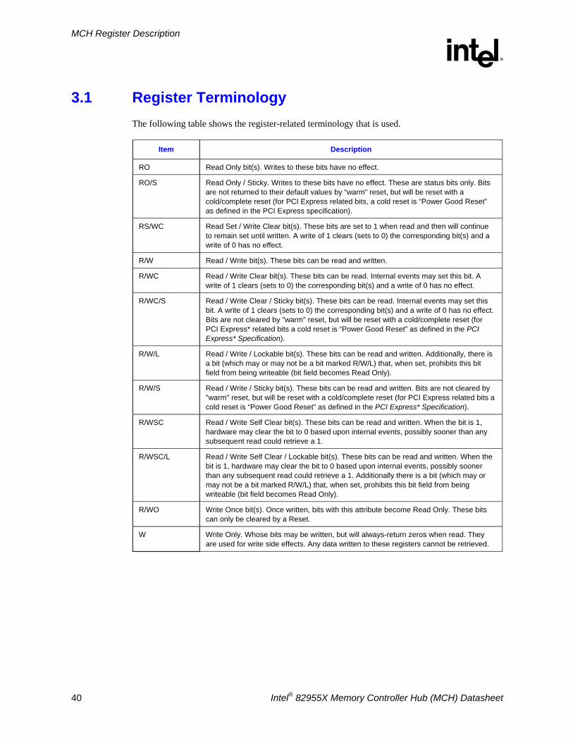
MCH Register Description
R
40 Intel® 82955X Memory Controller Hub (MCH) Datasheet
3.1 Register Terminology The following table shows the register-related terminology that is used.
Item Description
RO Read Only bit(s). Writes to these bits have no effect.
RO/S Read Only / Sticky. Writes to these bits have no effect. These are status bits only. Bits are not returned to their default values by “warm” reset, but will be reset with a cold/complete reset (for PCI Express related bits, a cold reset is “Power Good Reset” as defined in the PCI Express specification).
RS/WC Read Set / Write Clear bit(s). These bits are set to 1 when read and then will continue to remain set until written. A write of 1 clears (sets to 0) the corresponding bit(s) and a write of 0 has no effect.
R/W Read / Write bit(s). These bits can be read and written.
R/WC Read / Write Clear bit(s). These bits can be read. Internal events may set this bit. A write of 1 clears (sets to 0) the corresponding bit(s) and a write of 0 has no effect.
R/WC/S Read / Write Clear / Sticky bit(s). These bits can be read. Internal events may set this bit. A write of 1 clears (sets to 0) the corresponding bit(s) and a write of 0 has no effect. Bits are not cleared by "warm" reset, but will be reset with a cold/complete reset (for PCI Express* related bits a cold reset is “Power Good Reset” as defined in the PCI Express* Specification).
R/W/L Read / Write / Lockable bit(s). These bits can be read and written. Additionally, there is a bit (which may or may not be a bit marked R/W/L) that, when set, prohibits this bit field from being writeable (bit field becomes Read Only).
R/W/S Read / Write / Sticky bit(s). These bits can be read and written. Bits are not cleared by "warm" reset, but will be reset with a cold/complete reset (for PCI Express related bits a cold reset is “Power Good Reset” as defined in the PCI Express* Specification).
R/WSC Read / Write Self Clear bit(s). These bits can be read and written. When the bit is 1, hardware may clear the bit to 0 based upon internal events, possibly sooner than any subsequent read could retrieve a 1.
R/WSC/L Read / Write Self Clear / Lockable bit(s). These bits can be read and written. When the bit is 1, hardware may clear the bit to 0 based upon internal events, possibly sooner than any subsequent read could retrieve a 1. Additionally there is a bit (which may or may not be a bit marked R/W/L) that, when set, prohibits this bit field from being writeable (bit field becomes Read Only).
R/WO Write Once bit(s). Once written, bits with this attribute become Read Only. These bits can only be cleared by a Reset.
W Write Only. Whose bits may be written, but will always-return zeros when read. They are used for write side effects. Any data written to these registers cannot be retrieved.
MCH Register Description
R
Intel® 82955X Memory Controller Hub (MCH) Datasheet 41
3.2 Platform Configuration In platforms that support DMI (such as this MCH) the configuration structure is significantly different from previous hub architectures. The DMI physically connects the MCH and the ICH7; so, from a configuration standpoint, the DMI is logically PCI bus 0. As a result, all devices internal to the MCH and the ICH7 appear to be on PCI bus 0.
Note: The ICH7 internal LAN controller does not appear on bus 0; it appears on the external PCI bus and this number is configurable.
The system’s primary PCI expansion bus is physically attached to the ICH7 and, from a configuration perspective, appears to be a hierarchical PCI bus behind a PCI-to-PCI bridge; therefore, it has a programmable PCI Bus number. The PCI Express graphics attach appears to system software to be a real PCI bus behind a PCI-to-PCI bridge that is a device resident on PCI bus 0.
Note: A physical PCI bus 0 does not exist; DMI and the internal devices in the MCH and ICH7 logically constitute PCI Bus 0 to configuration software (see Figure 3-1).
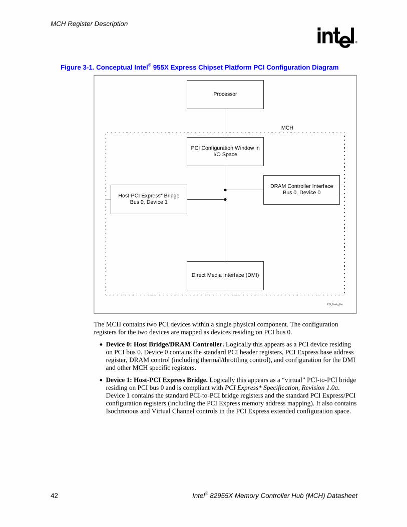
MCH Register Description
R
42 Intel® 82955X Memory Controller Hub (MCH) Datasheet
Figure 3-1. Conceptual Intel® 955X Express Chipset Platform PCI Configuration Diagram
Processor
PCI Configuration Window inI/O Space
Host-PCI Express* BridgeBus 0, Device 1
DRAM Controller InterfaceBus 0, Device 0
Direct Media Interface (DMI)
PCI_Config_Dia
MCH
The MCH contains two PCI devices within a single physical component. The configuration registers for the two devices are mapped as devices residing on PCI bus 0.
• Device 0: Host Bridge/DRAM Controller. Logically this appears as a PCI device residing on PCI bus 0. Device 0 contains the standard PCI header registers, PCI Express base address register, DRAM control (including thermal/throttling control), and configuration for the DMI and other MCH specific registers.
• Device 1: Host-PCI Express Bridge. Logically this appears as a “virtual” PCI-to-PCI bridge residing on PCI bus 0 and is compliant with PCI Express* Specification, Revision 1.0a. Device 1 contains the standard PCI-to-PCI bridge registers and the standard PCI Express/PCI configuration registers (including the PCI Express memory address mapping). It also contains Isochronous and Virtual Channel controls in the PCI Express extended configuration space.
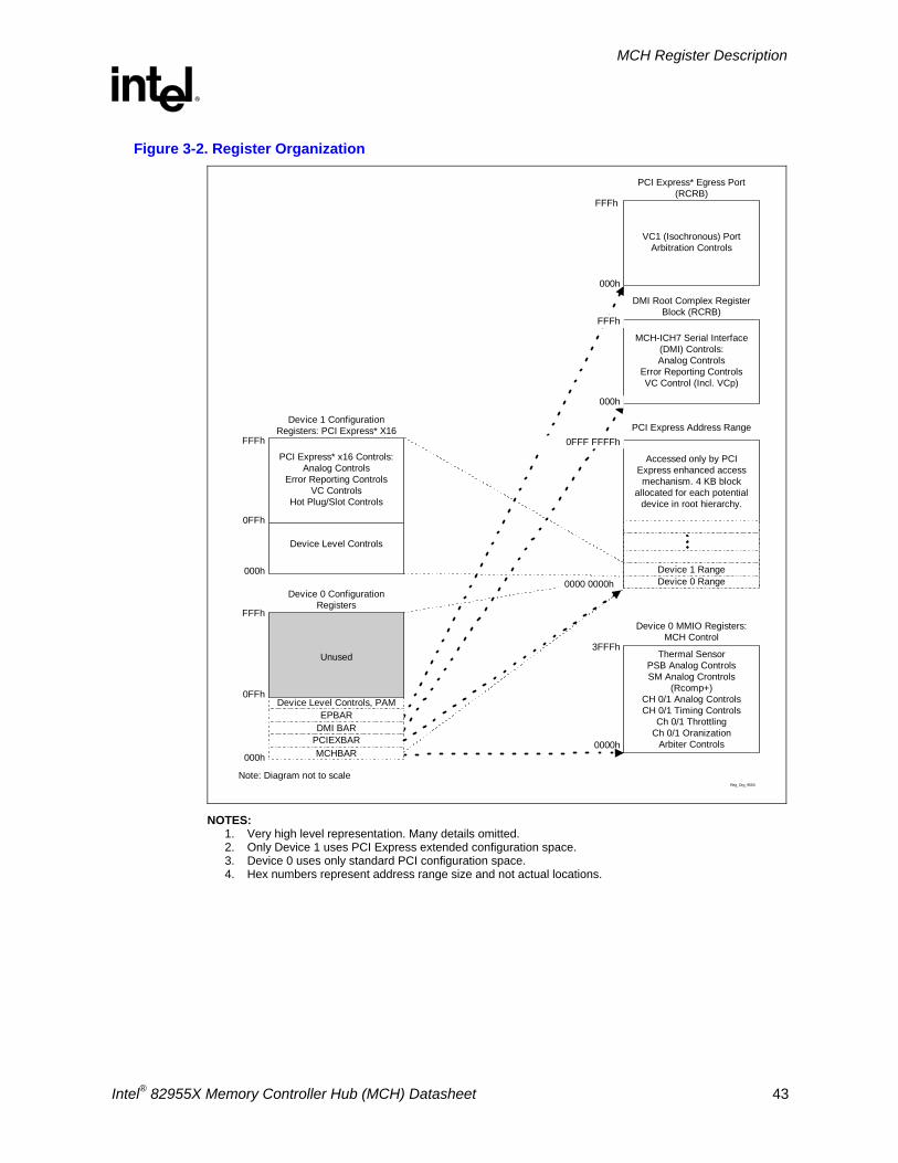
MCH Register Description
R
Intel® 82955X Memory Controller Hub (MCH) Datasheet 43
Figure 3-2. Register Organization
000h
VC1 (Isochronous) PortArbitration Controls
Reg_Org_955X
MCH-ICH7 Serial Interface(DMI) Controls:Analog Controls
Error Reporting ControlsVC Control (Incl. VCp)
PCI Express* Egress Port(RCRB)
DMI Root Complex RegisterBlock (RCRB)
Accessed only by PCIExpress enhanced accessmechanism. 4 KB block
allocated for each potentialdevice in root hierarchy.
PCI Express Address Range
Device 1 RangeDevice 0 Range
Thermal SensorPSB Analog ControlsSM Analog Crontrols
(Rcomp+)CH 0/1 Analog ControlsCH 0/1 Timing Controls
Ch 0/1 ThrottlingCh 0/1 Oranization
Arbiter Controls
Device 0 MMIO Registers:MCH Control
Unused
Device 0 ConfigurationRegisters
Device Level Controls, PAMEPBAR
DMI BARPCIEXBARMCHBAR000h
0FFh
FFFh
PCI Express* x16 Controls:Analog Controls
Error Reporting ControlsVC Controls
Hot Plug/Slot Controls
Device 1 ConfigurationRegisters: PCI Express* X16
Device Level Controls
000h
0FFh
FFFh
Note: Diagram not to scale
0000h
3FFFh
0000 0000h
0FFF FFFFh
000h
FFFh
FFFh
Unused
NOTES: 1. Very high level representation. Many details omitted. 2. Only Device 1 uses PCI Express extended configuration space. 3. Device 0 uses only standard PCI configuration space. 4. Hex numbers represent address range size and not actual locations.
MCH Register Description
R
44 Intel® 82955X Memory Controller Hub (MCH) Datasheet
3.3 Configuration Mechanisms The processor is the originator of configuration cycles so the FSB is the only interface in the platform where these mechanisms are used. The MCH translates transactions received through both configuration mechanisms to the same format.
3.3.1 Standard PCI Configuration Mechanism
The following is the mechanism for translating processor I/O bus cycles to configuration cycles.
The PCI Local Bus Specification defines a slot based "configuration space" that allows each device to contain up to 8 functions with each function containing up to 256 8-bit configuration registers. The PCI specification defines two bus cycles to access the PCI configuration space: Configuration Read and Configuration Write. Memory and I/O spaces are supported directly by the processor. Configuration space is supported by a mapping mechanism implemented within the MCH.
The configuration access mechanism makes use of the CONFIG_ADDRESS Register (at I/O address 0CF8h though 0CFBh) and the CONFIG_DATA Register (at I/O address 0CFCh though 0CFFh). To reference a configuration register a DWord I/O write cycle is used to place a value into CONFIG_ADDRESS that specifies the PCI bus, the device on that bus, the function within the device, and a specific configuration register of the device function being accessed. CONFIG_ADDRESS[31] must be 1 to enable a configuration cycle. CONFIG_DATA then becomes a window into the four bytes of configuration space specified by the contents of CONFIG_ADDRESS. Any read or write to CONFIG_DATA will result in the MCH translating the CONFIG_ADDRESS into the appropriate configuration cycle.
The MCH is responsible for translating and routing the processor’s I/O accesses to the CONFIG_ADDRESS and CONFIG_DATA registers to internal MCH configuration registers, DMI or PCI Express.
3.3.2 PCI Express* Enhanced Configuration Mechanism
PCI Express extends the configuration space to 4096 bytes per device/function as compared to 256 bytes allowed by PCI Local Bus Specification, Revision 2.3. PCI Express configuration space is divided into a PCI 2.3 compatible region that consists of the first 256B of a logical device’s configuration space and a PCI Express extended region that consists of the remaining configuration space.
The PCI compatible region can be accessed using either the Standard PCI Configuration Mechanism or using the PCI Express enhanced configuration mechanism described in this section. The extended configuration registers may only be accessed using the PCI Express enhanced configuration mechanism. To maintain compatibility with PCI configuration addressing mechanisms, system software must access the extended configuration space using 32-bit operations (32-bit aligned) only. These 32-bit operations include byte enables allowing only appropriate bytes within the DWord to be accessed. Locked transactions to the PCI Express memory mapped configuration address space are not supported. All changes made using either access mechanism are equivalent.
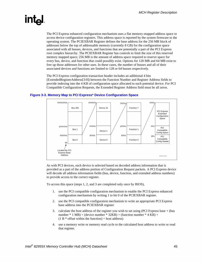
MCH Register Description
R
Intel® 82955X Memory Controller Hub (MCH) Datasheet 45
The PCI Express enhanced configuration mechanism uses a flat memory-mapped address space to access device configuration registers. This address space is reported by the system firmware to the operating system. The PCIEXBAR Register defines the base address for the 256 MB block of addresses below the top of addressable memory (currently 8 GB) for the configuration space associated with all busses, devices, and functions that are potentially a part of the PCI Express root complex hierarchy. The PCIEXBAR Register has controls to limit the size of this reserved memory mapped space; 256 MB is the amount of address space required to reserve space for every bus, device, and function that could possibly exist. Options for 128 MB and 64 MB exist to free up those addresses for other uses. In these cases, the number of busses and all of their associated devices and functions are limited to 128 or 64 busses respectively.
The PCI Express configuration transaction header includes an additional 4 bits (ExtendedRegisterAddress[3:0]) between the Function Number and Register Address fields to provide indexing into the 4 KB of configuration space allocated to each potential device. For PCI Compatible Configuration Requests, the Extended Register Address field must be all zeros.
Figure 3-3. Memory Map to PCI Express* Device Configuration Space
MemMap_PCIExpress
Bus 255
FFFFFFFh
Bus 1
Bus 0
1FFFFFh
FFFFFh
0h
Device 31
FFFFFh
Device 1
Device 0
FFFFh
7FFFh
Function 7
7FFFh
Function 1
Function 0
1FFFh
FFFh
FFFh
PCICompatible
Config Space
PCICompatible
Config Header
FFh
3Fh
PCI ExpressExtended
ConfigurationSpace
Located By PCIExpress Base
Address
As with PCI devices, each device is selected based on decoded address information that is provided as a part of the address portion of Configuration Request packets. A PCI Express device will decode all address information fields (bus, device, function, and extended address numbers) to provide access to the correct register.
To access this space (steps 1, 2, and 3 are completed only once by BIOS),
1. use the PCI compatible configuration mechanism to enable the PCI Express enhanced configuration mechanism by writing 1 to bit 0 of the PCIEXBAR register.
2. use the PCI compatible configuration mechanism to write an appropriate PCI Express base address into the PCIEXBAR register
3. calculate the host address of the register you wish to set using (PCI Express base + (bus number * 1 MB) + (device number * 32KB) + (function number * 4 KB) + (1 B * offset within the function) = host address)
4. use a memory write or memory read cycle to the calculated host address to write or read that register.
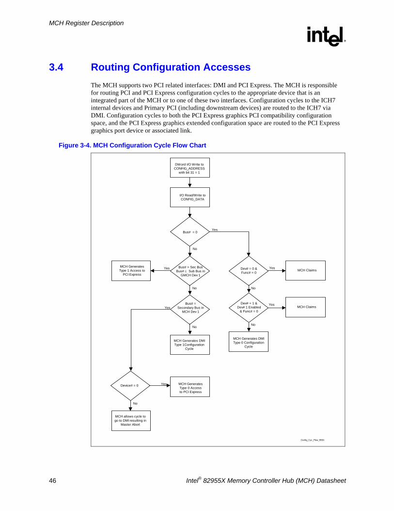
MCH Register Description
R
46 Intel® 82955X Memory Controller Hub (MCH) Datasheet
3.4 Routing Configuration Accesses The MCH supports two PCI related interfaces: DMI and PCI Express. The MCH is responsible for routing PCI and PCI Express configuration cycles to the appropriate device that is an integrated part of the MCH or to one of these two interfaces. Configuration cycles to the ICH7 internal devices and Primary PCI (including downstream devices) are routed to the ICH7 via DMI. Configuration cycles to both the PCI Express graphics PCI compatibility configuration space, and the PCI Express graphics extended configuration space are routed to the PCI Express graphics port device or associated link.
Figure 3-4. MCH Configuration Cycle Flow Chart
DWord I/O Write toCONFIG_ADDRESS
with bit 31 = 1
I/O Read/Write toCONFIG_DATA
MCH GeneratesType 1 Access to
PCI Express
MCH allows cycle togo to DMI resulting in
Master Abort
Bus# > Sec BusBus# ≤ Sub Bus in
GMCH Dev 1
Bus# = 0
Dev# = 1 &Dev# 1 Enabled
& Func# = 0
Dev# = 0 &Func# = 0
MCH Generates DMIType 1Configuration
Cycle
Bus# =Secondary Bus in
MCH Dev 1
MCH Generates DMIType 0 Configuration
Cycle
MCH Claims
MCH Claims
Yes
No
Yes
Yes
No
No
Yes
Yes
No
No
No
Device# = 0 MCH GeneratesType 0 Accessto PCI Express
Yes
Config_Cyc_Flow_955X
MCH Register Description
R
Intel® 82955X Memory Controller Hub (MCH) Datasheet 47
3.4.1 Internal Device Configuration Accesses
The MCH decodes the Bus Number (bits 23:16) and the Device Number fields of the CONFIG_ADDRESS register. If the Bus Number field of CONFIG_ADDRESS is 0, the configuration cycle is targeting a PCI Bus #0 device. If the targeted PCI Bus #0 device exists in the MCH and is not disabled, the configuration cycle is claimed by the appropriate device.
3.4.2 Bridge Related Configuration Accesses
Configuration accesses on PCI Express or DMI are PCI Express configuration TLPs (Transaction Layer Packets):
• Bus Number [7:0] is Header Byte 8 [7:0]
• Device Number [4:0] is Header Byte 9 [7:3]
• Function Number [2:0] is Header Byte 9 [2:0]
And special fields for this type of TLP:
• Extended Register Number [3:0] is Header Byte 10 [3:0]
• Register Number [5:0] is Header Byte 11 [7:2]
See the PCI Express specification for more information on both the PCI 2.3 compatible and PCI Express enhanced configuration mechanism and transaction rules.
3.4.2.1 PCI Express* Configuration Accesses
When the Bus Number of a type 1 Standard PCI Configuration cycle or PCI Express enhanced configuration access matches the Device #1 Secondary Bus Number, a PCI Express Type 0 configuration TLP is generated on the PCI Express link targeting the device directly on the opposite side of the link. This should be Device #0 on the bus number assigned to the PCI Express link (likely Bus #1).
The device on other side of link must be Device #0. The MCH will Master Abort any Type 0 configuration access to a non-zero Device number. If there is to be more than one device on that side of the link, there must be a bridge implemented in the downstream device.
When the Bus Number of a type 1 Standard PCI Configuration cycle or PCI Express enhanced configuration access is within the claimed range (between the upper bound of the bridge device’s Subordinate Bus Number register and the lower bound of the bridge device’s Secondary Bus Number register) but does not match the Device #1 Secondary Bus Number, a PCI Express Type 1 configuration TLP is generated on the secondary side of the PCI Express link.
PCI Express Configuration Writes:
• Internally, the host interface unit translates writes to PCI Express extended configuration space to configuration writes on the backbone.
• Writes to extended space are posted on the FSB, but non-posted on the PCI Express or DMI (i.e., translated to configuration writes).
MCH Register Description
R
48 Intel® 82955X Memory Controller Hub (MCH) Datasheet
3.4.2.2 DMI Configuration Accesses
Accesses to disabled MCH internal devices, bus numbers not claimed by the Host-PCI Express bridge, or PCI Bus #0 devices not part of the MCH (#2 through #31) will subtractively decode to the ICH7 and, consequently, be forwarded over the DMI via a PCI Express configuration TLP.
If the Bus Number is zero, the MCH will generate a Type 0 Configuration Cycle TLP on DMI. If the Bus Number is non-zero, and falls outside the range claimed by the Host-PCI Express bridge, the MCH will generate a Type 1 configuration cycle TLP on DMI.
The ICH7 routes configuration accesses in a manner similar to the MCH. The ICH7 decodes the configuration TLP and generates a corresponding configuration access. Accesses targeting a device on PCI Bus #0 may be claimed by an internal device. The ICH7 compares the non-zero Bus Number with the Secondary Bus Number and Subordinate Bus Number registers of its PCI-to-PCI bridges to determine if the configuration access is meant for Primary PCI, one of the ICH7’s devices, the DMI, or some other downstream PCI bus or PCI Express link.
Configuration accesses that are forwarded to the ICH7, but remain unclaimed by any device or bridge will result in a master abort.
3.5 I/O Mapped Registers The MCH contains two registers that reside in the processor I/O address space: the Configuration Address (CONFIG_ADDRESS) Register and the Configuration Data (CONFIG_DATA) Register. The Configuration Address Register enables/disables the configuration space and determines what portion of configuration space is visible through the Configuration Data window.
3.5.1 CONFIG_ADDRESS—Configuration Address Register I/O Address: 0CF8–0CFBh Accessed as a DW Default Value: 00000000h Access: R/W Size: 32 bits
CONFIG_ADDRESS is a 32-bit register that can be accessed only as a DWord. A Byte or Word reference will "pass through" the Configuration Address Register and DMI onto the Primary PCI bus as an I/O cycle. The CONFIG_ADDRESS register contains the Bus Number, Device Number, Function Number, and Register Number for which a subsequent configuration access is intended.
Bit Access &
Default
Description
31 R/W 0b
Configuration Enable (CFGE)
1 = Enable. Accesses to PCI configuration space are enabled
0 = Disable.
30:24 Reserved
MCH Register Description
R
Intel® 82955X Memory Controller Hub (MCH) Datasheet 49
Bit Access &
Default
Description
23:16 R/W 00h
Bus Number: If the Bus Number is programmed to 00h, the target of the configuration cycle is a PCI Bus #0 agent. If this is the case and the MCH is not the target (i.e., the device number is ≥ 2), then a DMI Type 0 configuration cycle is generated.
If the Bus Number is non-zero, and does not fall within the ranges enumerated by device 1’s Secondary Bus Number or Subordinate Bus Number Register, then a DMI Type 1 configuration cycle is generated.
If the Bus Number is non-zero and matches the value programmed into the Secondary Bus Number Register of device 1, a Type 0 PCI configuration cycle will be generated on PCI Express.
If the Bus Number is non-zero, greater than the value in the Secondary Bus Number register of device 1 and less than or equal to the value programmed into the Subordinate Bus Number Register of device 1, a Type 1 PCI configuration cycle will be generated on PCI Express.
This field is mapped to byte 8 [7:0] of the request header format during PCI Express configuration cycles and A[23:16] during the DMI Type 1 configuration cycles.
15:11 R/W 00h
Device Number: This field selects one agent on the PCI bus selected by the Bus Number. When the Bus Number field is “00”, the MCH decodes the Device Number field. The MCH is always Device Number 0 for the Host bridge entity, Device Number 1 for the Host-PCI Express entity. Therefore, when the Bus Number =0 and the Device Number equals 0, or 1, the internal MCH devices are selected.
This field is mapped to byte 6 [7:3] of the request header format during PCI Express configuration cycles and A[15:11] during the DMI configuration cycles.
10:8 R/W 000b
Function Number: This field allows the configuration registers of a particular function in a multi-function device to be accessed. The MCH ignores configuration cycles to its internal devices if the function number is not equal to 0.
This field is mapped to byte 6 [2:0] of the request header format during PCI Express configuration cycles and A[10:8] during the DMI configuration cycles.
7:2 R/W 00h
Register Number: This field selects one register within a particular Bus, Device, and Function as specified by the other fields in the Configuration Address Register.
This field is mapped to byte 7 [7:2] of the request header format during PCI Express configuration cycles and A[7:2] during the DMI Configuration cycles.
1:0 Reserved
MCH Register Description
R
50 Intel® 82955X Memory Controller Hub (MCH) Datasheet
3.5.2 CONFIG_DATA—Configuration Data Register I/O Address: 0CFCh–0CFF Default Value: 00000000h Access: R/W Size: 32 bits
CONFIG_DATA is a 32-bit read/write window into configuration space. The portion of configuration space that is referenced by CONFIG_DATA is determined by the contents of CONFIG_ADDRESS.
Bit Access & Default
Description
31:0 R/W 0000 0000h
Configuration Data Window (CDW): If bit 31 of CONFIG_ADDRESS is 1, any I/O access to the CONFIG_DATA register will produce a configuration transaction using the contents of CONFIG_ADDRESS to determine the bus, device, function, and offset of the register to be accessed.
§
Host Bridge Registers (D0:F0)
R
Intel® 82955X Memory Controller Hub (MCH) Datasheet 51
4 Host Bridge Registers (D0:F0) This chapter contains the host bridge registers that are in Device 0 (D0), Function 0 (F0). The DRAM Controller registers are in D0:F0. Table 4-1 is an address map for D0:F0; registers are listed by address offset in ascending order. Section 4.1 provides detailed bit descriptions of the registers listed in Table 4-1. All registers that are defined in the PCI 2.3 specification, but are not necessary or implemented in this component are not included in this document.
Warning: Address locations that are not listed are considered Intel Reserved register locations. Reads to Reserved address locations may return non-zero values. Writes to reserved locations may cause system failures.
Table 4-1. Host Bridge Register Address Map (D0:F0)
Address Offset Symbol Register Name Default
Value Access
00–01h VID Vendor Identification 8086h RO
02–03h DID Device Identification 2774h RO
04–05h PCICMD PCI Command 0006h RO, R/W
06–07h PCISTS PCI Status 0090h RO, R/W/C
08h RID Revision Identification See register description
RO
09–0Bh CC Class Code 060000h RO
0Ch — Reserved — —
0Dh MLT Master Latency Timer 00h RO
0Eh HDR Header Type 00h RO
0F–2Bh — Reserved — —
2C–2Dh SVID Subsystem Vendor Identification 0000h R/WO
2E–2Fh SID Subsystem Identification 0000h R/WO
30–33h — Reserved — —
34h CAPPTR Capabilities Pointer E0h RO
35–3Fh — Reserved — —
40–43h EPBAR Egress Port Base Address 00000000h RO
44–47h MCHBAR MCH Memory Mapped Register Range Base Address
00000000h R/W
48–4Bh PCIEXBAR PCI Express* Register Range Base Address
E0000000h R/W
4C–4Fh DMIBAR Root Complex Register Range Base Address
00000000h R/W
50–53h — Reserved — —
Host Bridge Registers (D0:F0)
R
52 Intel® 82955X Memory Controller Hub (MCH) Datasheet
Address Offset Symbol Register Name Default
Value Access
54–57h DEVEN Device Enable 00000003h R/W
58–5Bh DEAP DRAM Error Address 00000000h RO/S
5Ch DERRSYN DRAM Error Syndrome 00h RO/S
5Dh DERRDST DRAM Error Destination 00h RO/S
5E–8Fh — Reserved — —
90h PAM0 Programmable Attribute Map 0 00h R/W
91h PAM1 Programmable Attribute Map 1 00h R/W
92h PAM2 Programmable Attribute Map 2 00h R/W
93h PAM3 Programmable Attribute Map 3 00h R/W
94h PAM4 Programmable Attribute Map 4 00h R/W
95h PAM5 Programmable Attribute Map 5 00h R/W
96h PAM6 Programmable Attribute Map 6 00h R/W
97h LAC Legacy Access Control 00h R/W
98–99h REMAPBASE Remap Base Address 03FFh RW
9A–9Bh REMAPLIMIT Remap Limit Address 0000h RW
9Ch TOLUD Top of Low Usable DRAM 08h R/W
9Dh SMRAM System Management RAM Control 02h RO, R/W/L
9Eh ESMRAMC Extended System Management RAM Control
38h RO, R/W/L
9Fh — Reserved — —
A0–A1h TOM Top of Memory 0001h R/W
A2–C7h — Reserved — —
C8–C9h ERRSTS Error Status 0000h RO, R/WC/S
CA–CBh ERRCMD Error Command 0000h R/W
CC–CDh SMICMD SMI Command 0000h RO, R/W
CE–CFh SCICMD SCI Command 0000h RO, R/W
DA–DBh — Reserved — —
DC–DFh SKPD Scratchpad Data 00000000h R/W
E0–E8h CAPID0 Capability Identifier 000000000001090009h
RO
FCh EDEAP Extended DRAM Error Address Pointer 00h RO/S
Host Bridge Registers (D0:F0)
R
Intel® 82955X Memory Controller Hub (MCH) Datasheet 53
4.1 Configuration Register Details (D1:F0)
4.1.1 VID—Vendor Identification (D0:F0) PCI Device: 0 Address Offset: 00–01h Default Value: 8086h Access: RO Size: 16 bits
This register combined, with the Device Identification register, uniquely identifies any PCI device.
Bit Access & Default
Description
15:0 RO 8086h
Vendor Identification Number (VID): PCI standard identification for Intel.
4.1.2 DID—Device Identification (D0:F0) PCI Device: 0 Address Offset: 02–03h Default Value: 2774h Access: RO Size: 16 bits
This register, combined with the Vendor Identification register, uniquely identifies any PCI device.
Bit Access & Default
Description
15:0 RO 2774h
Device Identification Number (DID): Identifier assigned to the MCH core/primary PCI device.
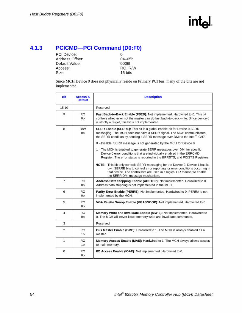
Host Bridge Registers (D0:F0)
R
54 Intel® 82955X Memory Controller Hub (MCH) Datasheet
4.1.3 PCICMD—PCI Command (D0:F0) PCI Device: 0 Address Offset: 04–05h Default Value: 0006h Access: RO, R/W Size: 16 bits
Since MCH Device 0 does not physically reside on Primary PCI bus, many of the bits are not implemented.
Bit Access & Default
Description
15:10 Reserved
9 RO 0b
Fast Back-to-Back Enable (FB2B): Not implemented. Hardwired to 0. This bit controls whether or not the master can do fast back-to-back write. Since device 0 is strictly a target, this bit is not implemented.
8 R/W 0b
SERR Enable (SERRE): This bit is a global enable bit for Device 0 SERR messaging. The MCH does not have a SERR signal. The MCH communicates the SERR condition by sending a SERR message over DMI to the Intel® ICH7.
0 = Disable. SERR message is not generated by the MCH for Device 0
1 = The MCH is enabled to generate SERR messages over DMI for specific Device 0 error conditions that are individually enabled in the ERRCMD Register. The error status is reported in the ERRSTS, and PCISTS Registers.
NOTE: This bit only controls SERR messaging for the Device 0. Device 1 has its own SERRE bits to control error reporting for error conditions occurring in that device. The control bits are used in a logical OR manner to enable the SERR DMI message mechanism.
7 RO 0b
Address/Data Stepping Enable (ADSTEP): Not implemented. Hardwired to 0. Address/data stepping is not implemented in the MCH.
6 RO 0b
Parity Error Enable (PERRE): Not implemented. Hardwired to 0. PERR# is not implemented by the MCH.
5 RO 0b
VGA Palette Snoop Enable (VGASNOOP): Not implemented. Hardwired to 0..
4 RO 0b
Memory Write and Invalidate Enable (MWIE): Not implemented. Hardwired to 0. The MCH will never issue memory write and invalidate commands.
3 Reserved
2 RO 1b
Bus Master Enable (BME): Hardwired to 1. The MCH is always enabled as a master.
1 RO 1b
Memory Access Enable (MAE): Hardwired to 1. The MCH always allows access to main memory.
0 RO 0b
I/O Access Enable (IOAE): Not implemented. Hardwired to 0.
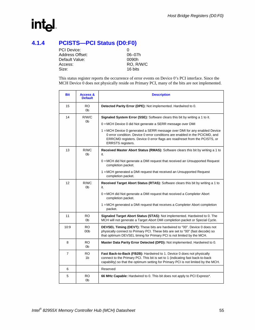
Host Bridge Registers (D0:F0)
R
Intel® 82955X Memory Controller Hub (MCH) Datasheet 55
4.1.4 PCISTS—PCI Status (D0:F0) PCI Device: 0 Address Offset: 06–07h Default Value: 0090h Access: RO, R/W/C Size: 16 bits
This status register reports the occurrence of error events on Device 0’s PCI interface. Since the MCH Device 0 does not physically reside on Primary PCI, many of the bits are not implemented.
Bit Access & Default
Description
15 RO 0b
Detected Parity Error (DPE): Not implemented. Hardwired to 0.
14 R/W/C 0b
Signaled System Error (SSE): Software clears this bit by writing a 1 to it.
0 = MCH Device 0 did Not generate a SERR message over DMI
1 = MCH Device 0 generated a SERR message over DMI for any enabled Device 0 error condition. Device 0 error conditions are enabled in the PCICMD, and ERRCMD registers. Device 0 error flags are read/reset from the PCISTS, or ERRSTS registers.
13 R/WC 0b
Received Master Abort Status (RMAS): Software clears this bit by writing a 1 to it.
0 = MCH did Not generate a DMI request that received an Unsupported Request completion packet.
1 = MCH generated a DMI request that received an Unsupported Request completion packet.
12 R/WC 0b
Received Target Abort Status (RTAS): Software clears this bit by writing a 1 to it.
0 = MCH did Not generate a DMI request that received a Completer Abort completion packet.
1 = MCH generated a DMI request that receives a Completer Abort completion packet.
11 RO 0b
Signaled Target Abort Status (STAS): Not implemented. Hardwired to 0. The MCH will not generate a Target Abort DMI completion packet or Special Cycle.
10:9 RO 00b
DEVSEL Timing (DEVT): These bits are hardwired to "00". Device 0 does not physically connect to Primary PCI. These bits are set to "00" (fast decode) so that optimum DEVSEL timing for Primary PCI is not limited by the MCH.
8 RO 0b
Master Data Parity Error Detected (DPD): Not implemented. Hardwired to 0.
7 RO 1b
Fast Back-to-Back (FB2B): Hardwired to 1. Device 0 does not physically connect to the Primary PCI. This bit is set to 1 (indicating fast back-to-back capability) so that the optimum setting for Primary PCI is not limited by the MCH.
6 Reserved
5 RO 0b
66 MHz Capable: Hardwired to 0. This bit does not apply to PCI Express*.
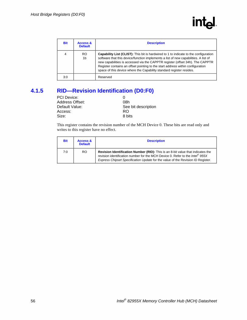
Host Bridge Registers (D0:F0)
R
56 Intel® 82955X Memory Controller Hub (MCH) Datasheet
Bit Access & Default
Description
4 RO 1b
Capability List (CLIST): This bit is hardwired to 1 to indicate to the configuration software that this device/function implements a list of new capabilities. A list of new capabilities is accessed via the CAPPTR register (offset 34h). The CAPPTR Register contains an offset pointing to the start address within configuration space of this device where the Capability standard register resides.
3:0 Reserved
4.1.5 RID—Revision Identification (D0:F0) PCI Device: 0 Address Offset: 08h Default Value: See bit description Access: RO Size: 8 bits
This register contains the revision number of the MCH Device 0. These bits are read only and writes to this register have no effect.
Bit Access & Default
Description
7:0 RO Revision Identification Number (RID): This is an 8-bit value that indicates the revision identification number for the MCH Device 0. Refer to the Intel® 955X Express Chipset Specification Update for the value of the Revision ID Register.
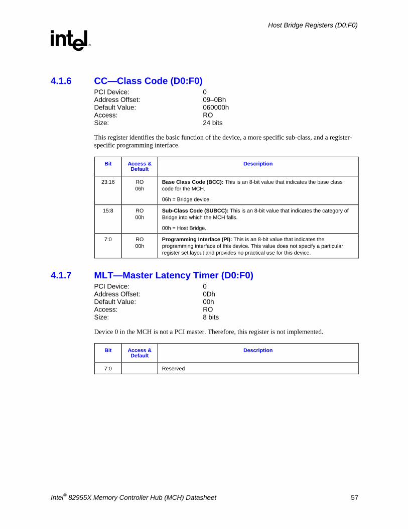
Host Bridge Registers (D0:F0)
R
Intel® 82955X Memory Controller Hub (MCH) Datasheet 57
4.1.6 CC—Class Code (D0:F0) PCI Device: 0 Address Offset: 09–0Bh Default Value: 060000h Access: RO Size: 24 bits
This register identifies the basic function of the device, a more specific sub-class, and a register-specific programming interface.
Bit Access & Default
Description
23:16 RO 06h
Base Class Code (BCC): This is an 8-bit value that indicates the base class code for the MCH.
06h = Bridge device.
15:8 RO 00h
Sub-Class Code (SUBCC): This is an 8-bit value that indicates the category of Bridge into which the MCH falls.
00h = Host Bridge.
7:0 RO 00h
Programming Interface (PI): This is an 8-bit value that indicates the programming interface of this device. This value does not specify a particular register set layout and provides no practical use for this device.
4.1.7 MLT—Master Latency Timer (D0:F0) PCI Device: 0 Address Offset: 0Dh Default Value: 00h Access: RO Size: 8 bits
Device 0 in the MCH is not a PCI master. Therefore, this register is not implemented.
Bit Access & Default
Description
7:0 Reserved
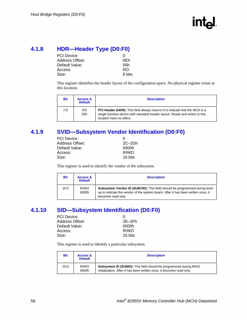
Host Bridge Registers (D0:F0)
R
58 Intel® 82955X Memory Controller Hub (MCH) Datasheet
4.1.8 HDR—Header Type (D0:F0) PCI Device: 0 Address Offset: 0Eh Default Value: 00h Access: RO Size: 8 bits
This register identifies the header layout of the configuration space. No physical register exists at this location.
Bit Access & Default
Description
7:0 RO 00h
PCI Header (HDR): This field always returns 0 to indicate that the MCH is a single function device with standard header layout. Reads and writes to this location have no effect.
4.1.9 SVID—Subsystem Vendor Identification (D0:F0) PCI Device: 0 Address Offset: 2C–2Dh Default Value: 0000h Access: R/WO Size: 16 bits
This register is used to identify the vendor of the subsystem.
Bit Access & Default
Description
15:0 R/WO 0000h
Subsystem Vendor ID (SUBVID): This field should be programmed during boot-up to indicate the vendor of the system board. After it has been written once, it becomes read only.
4.1.10 SID—Subsystem Identification (D0:F0) PCI Device: 0 Address Offset: 2E–2Fh Default Value: 0000h Access: R/WO Size: 16 bits
This register is used to identify a particular subsystem.
Bit Access & Default
Description
15:0 R/WO 0000h
Subsystem ID (SUBID): This field should be programmed during BIOS initialization. After it has been written once, it becomes read only.
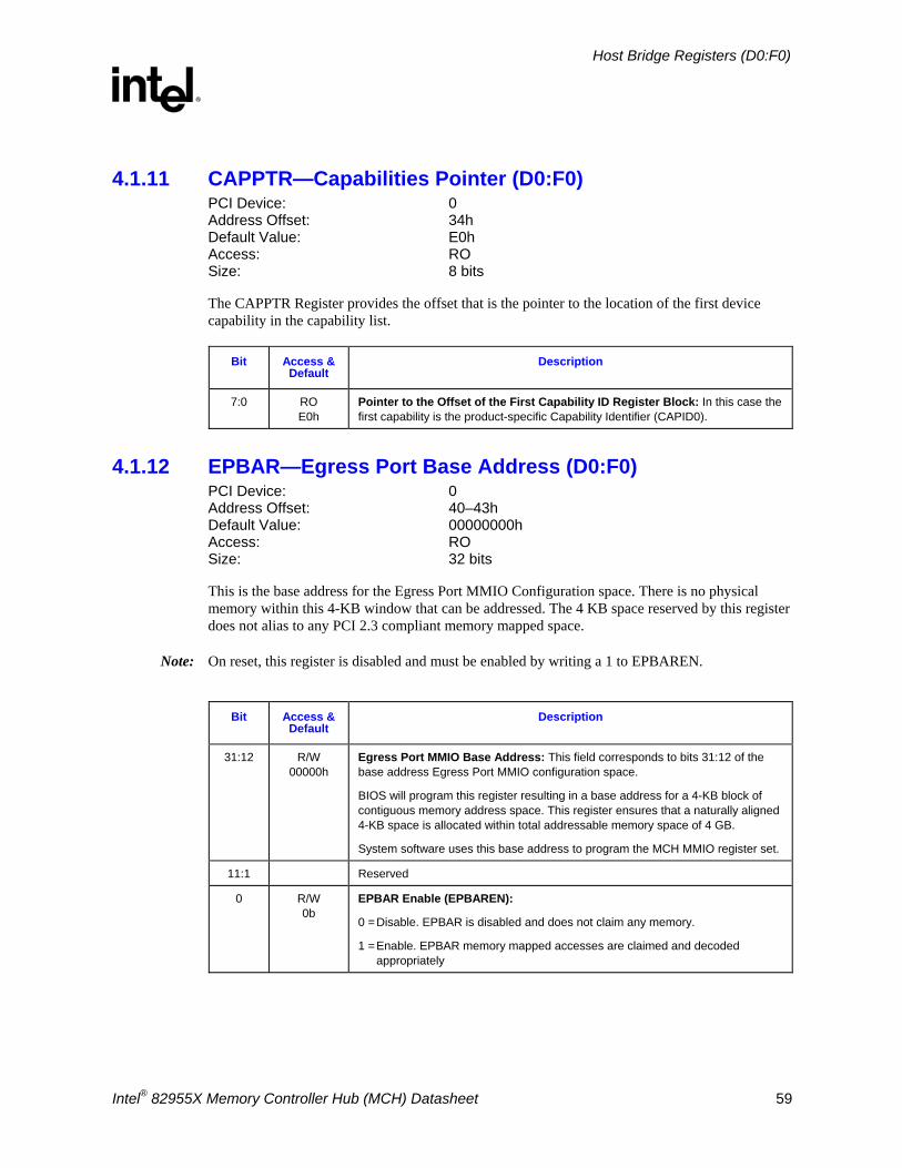
Host Bridge Registers (D0:F0)
R
Intel® 82955X Memory Controller Hub (MCH) Datasheet 59
4.1.11 CAPPTR—Capabilities Pointer (D0:F0) PCI Device: 0 Address Offset: 34h Default Value: E0h Access: RO Size: 8 bits
The CAPPTR Register provides the offset that is the pointer to the location of the first device capability in the capability list.
Bit Access & Default
Description
7:0 RO E0h
Pointer to the Offset of the First Capability ID Register Block: In this case the first capability is the product-specific Capability Identifier (CAPID0).
4.1.12 EPBAR—Egress Port Base Address (D0:F0) PCI Device: 0 Address Offset: 40–43h Default Value: 00000000h Access: RO Size: 32 bits
This is the base address for the Egress Port MMIO Configuration space. There is no physical memory within this 4-KB window that can be addressed. The 4 KB space reserved by this register does not alias to any PCI 2.3 compliant memory mapped space.
Note: On reset, this register is disabled and must be enabled by writing a 1 to EPBAREN.
Bit Access &
Default Description
31:12 R/W 00000h
Egress Port MMIO Base Address: This field corresponds to bits 31:12 of the base address Egress Port MMIO configuration space.
BIOS will program this register resulting in a base address for a 4-KB block of contiguous memory address space. This register ensures that a naturally aligned 4-KB space is allocated within total addressable memory space of 4 GB.
System software uses this base address to program the MCH MMIO register set.
11:1 Reserved
0 R/W 0b
EPBAR Enable (EPBAREN):
0 = Disable. EPBAR is disabled and does not claim any memory.
1 = Enable. EPBAR memory mapped accesses are claimed and decoded appropriately
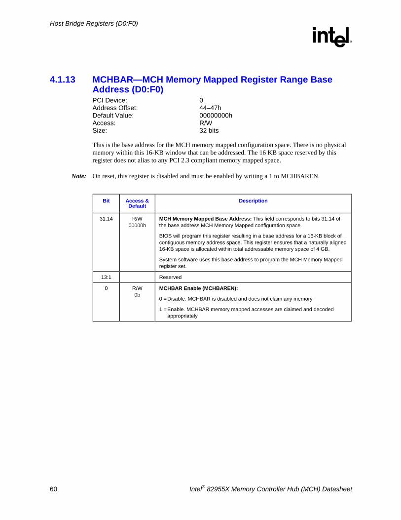
Host Bridge Registers (D0:F0)
R
60 Intel® 82955X Memory Controller Hub (MCH) Datasheet
4.1.13 MCHBAR—MCH Memory Mapped Register Range Base Address (D0:F0) PCI Device: 0 Address Offset: 44–47h Default Value: 00000000h Access: R/W Size: 32 bits
This is the base address for the MCH memory mapped configuration space. There is no physical memory within this 16-KB window that can be addressed. The 16 KB space reserved by this register does not alias to any PCI 2.3 compliant memory mapped space.
Note: On reset, this register is disabled and must be enabled by writing a 1 to MCHBAREN.
Bit Access &
Default Description
31:14 R/W 00000h
MCH Memory Mapped Base Address: This field corresponds to bits 31:14 of the base address MCH Memory Mapped configuration space.
BIOS will program this register resulting in a base address for a 16-KB block of contiguous memory address space. This register ensures that a naturally aligned 16-KB space is allocated within total addressable memory space of 4 GB.
System software uses this base address to program the MCH Memory Mapped register set.
13:1 Reserved
0 R/W 0b
MCHBAR Enable (MCHBAREN):
0 = Disable. MCHBAR is disabled and does not claim any memory
1 = Enable. MCHBAR memory mapped accesses are claimed and decoded appropriately
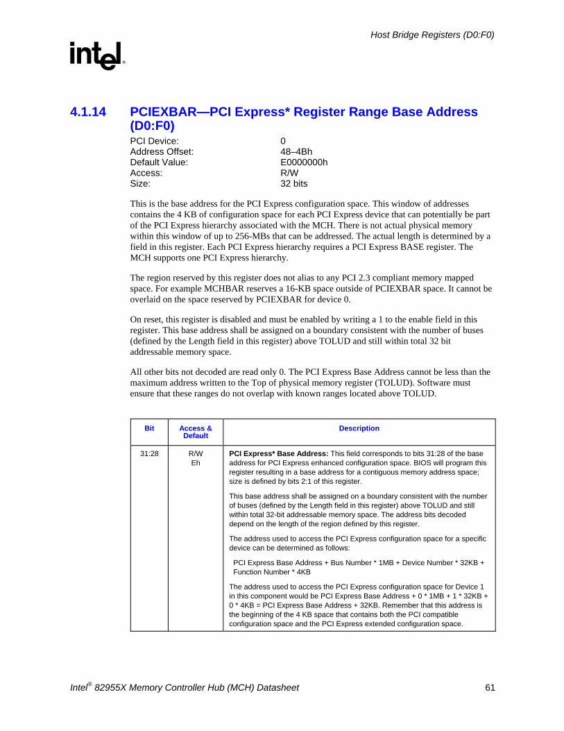
Host Bridge Registers (D0:F0)
R
Intel® 82955X Memory Controller Hub (MCH) Datasheet 61
4.1.14 PCIEXBAR—PCI Express* Register Range Base Address (D0:F0) PCI Device: 0 Address Offset: 48–4Bh Default Value: E0000000h Access: R/W Size: 32 bits
This is the base address for the PCI Express configuration space. This window of addresses contains the 4 KB of configuration space for each PCI Express device that can potentially be part of the PCI Express hierarchy associated with the MCH. There is not actual physical memory within this window of up to 256-MBs that can be addressed. The actual length is determined by a field in this register. Each PCI Express hierarchy requires a PCI Express BASE register. The MCH supports one PCI Express hierarchy.
The region reserved by this register does not alias to any PCI 2.3 compliant memory mapped space. For example MCHBAR reserves a 16-KB space outside of PCIEXBAR space. It cannot be overlaid on the space reserved by PCIEXBAR for device 0.
On reset, this register is disabled and must be enabled by writing a 1 to the enable field in this register. This base address shall be assigned on a boundary consistent with the number of buses (defined by the Length field in this register) above TOLUD and still within total 32 bit addressable memory space.
All other bits not decoded are read only 0. The PCI Express Base Address cannot be less than the maximum address written to the Top of physical memory register (TOLUD). Software must ensure that these ranges do not overlap with known ranges located above TOLUD.
Bit Access &
Default Description
31:28 R/W Eh
PCI Express* Base Address: This field corresponds to bits 31:28 of the base address for PCI Express enhanced configuration space. BIOS will program this register resulting in a base address for a contiguous memory address space; size is defined by bits 2:1 of this register.
This base address shall be assigned on a boundary consistent with the number of buses (defined by the Length field in this register) above TOLUD and still within total 32-bit addressable memory space. The address bits decoded depend on the length of the region defined by this register.
The address used to access the PCI Express configuration space for a specific device can be determined as follows:
PCI Express Base Address + Bus Number * 1MB + Device Number * 32KB + Function Number * 4KB
The address used to access the PCI Express configuration space for Device 1 in this component would be PCI Express Base Address + 0 * 1MB + 1 * 32KB + 0 * 4KB = PCI Express Base Address + 32KB. Remember that this address is the beginning of the 4 KB space that contains both the PCI compatible configuration space and the PCI Express extended configuration space.
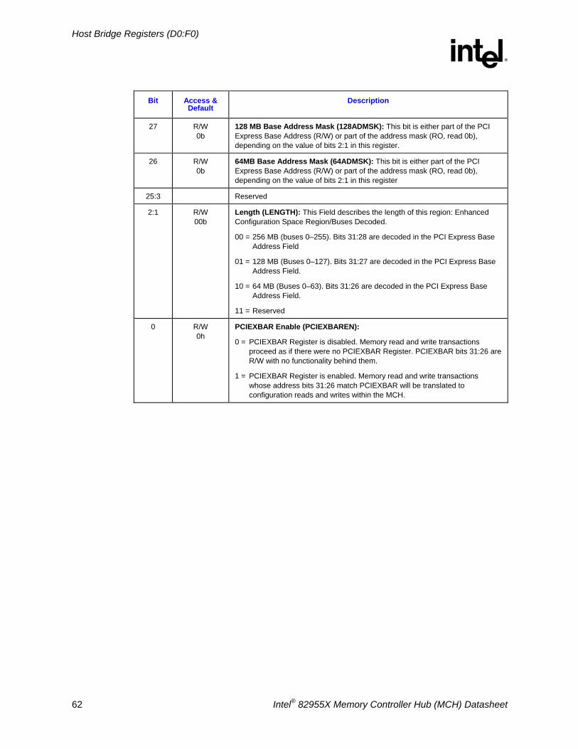
Host Bridge Registers (D0:F0)
R
62 Intel® 82955X Memory Controller Hub (MCH) Datasheet
Bit Access & Default
Description
27 R/W 0b
128 MB Base Address Mask (128ADMSK): This bit is either part of the PCI Express Base Address (R/W) or part of the address mask (RO, read 0b), depending on the value of bits 2:1 in this register.
26 R/W 0b
64MB Base Address Mask (64ADMSK): This bit is either part of the PCI Express Base Address (R/W) or part of the address mask (RO, read 0b), depending on the value of bits 2:1 in this register
25:3 Reserved
2:1 R/W 00b
Length (LENGTH): This Field describes the length of this region: Enhanced Configuration Space Region/Buses Decoded.
00 = 256 MB (buses 0–255). Bits 31:28 are decoded in the PCI Express Base Address Field
01 = 128 MB (Buses 0–127). Bits 31:27 are decoded in the PCI Express Base Address Field.
10 = 64 MB (Buses 0–63). Bits 31:26 are decoded in the PCI Express Base Address Field.
11 = Reserved
0 R/W 0h
PCIEXBAR Enable (PCIEXBAREN):
0 = PCIEXBAR Register is disabled. Memory read and write transactions proceed as if there were no PCIEXBAR Register. PCIEXBAR bits 31:26 are R/W with no functionality behind them.
1 = PCIEXBAR Register is enabled. Memory read and write transactions whose address bits 31:26 match PCIEXBAR will be translated to configuration reads and writes within the MCH.
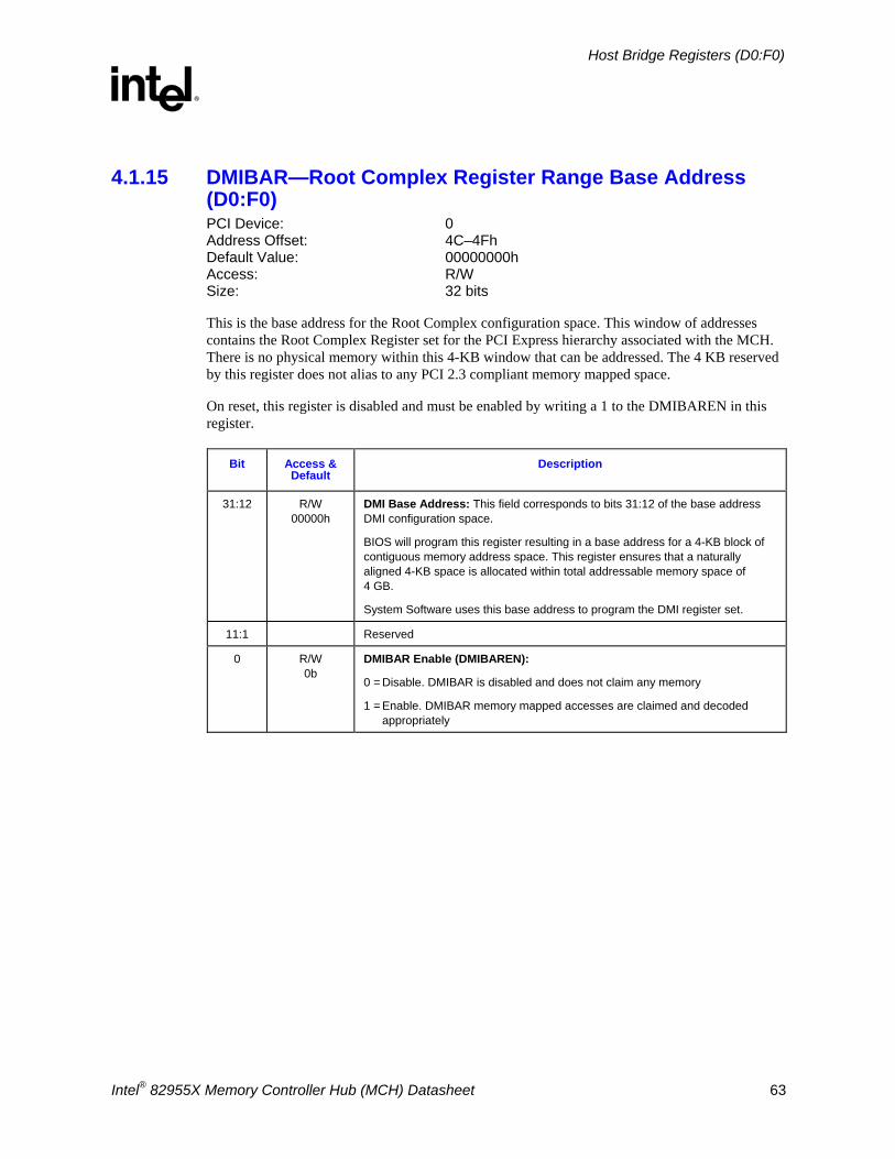
Host Bridge Registers (D0:F0)
R
Intel® 82955X Memory Controller Hub (MCH) Datasheet 63
4.1.15 DMIBAR—Root Complex Register Range Base Address (D0:F0) PCI Device: 0 Address Offset: 4C–4Fh Default Value: 00000000h Access: R/W Size: 32 bits
This is the base address for the Root Complex configuration space. This window of addresses contains the Root Complex Register set for the PCI Express hierarchy associated with the MCH. There is no physical memory within this 4-KB window that can be addressed. The 4 KB reserved by this register does not alias to any PCI 2.3 compliant memory mapped space.
On reset, this register is disabled and must be enabled by writing a 1 to the DMIBAREN in this register.
Bit Access & Default
Description
31:12 R/W 00000h
DMI Base Address: This field corresponds to bits 31:12 of the base address DMI configuration space.
BIOS will program this register resulting in a base address for a 4-KB block of contiguous memory address space. This register ensures that a naturally aligned 4-KB space is allocated within total addressable memory space of 4 GB.
System Software uses this base address to program the DMI register set.
11:1 Reserved
0 R/W 0b
DMIBAR Enable (DMIBAREN):
0 = Disable. DMIBAR is disabled and does not claim any memory
1 = Enable. DMIBAR memory mapped accesses are claimed and decoded appropriately
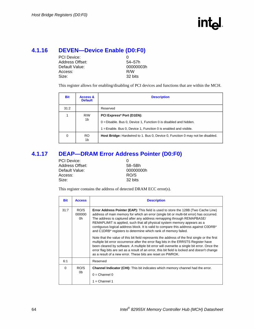
Host Bridge Registers (D0:F0)
R
64 Intel® 82955X Memory Controller Hub (MCH) Datasheet
4.1.16 DEVEN—Device Enable (D0:F0) PCI Device: 0 Address Offset: 54–57h Default Value: 00000003h Access: R/W Size: 32 bits
This register allows for enabling/disabling of PCI devices and functions that are within the MCH.
Bit Access & Default
Description
31:2 Reserved
1 R/W 1b
PCI Express* Port (D1EN):
0 = Disable. Bus 0, Device 1, Function 0 is disabled and hidden.
1 = Enable. Bus 0, Device 1, Function 0 is enabled and visible.
0 RO 1b
Host Bridge: Hardwired to 1. Bus 0, Device 0, Function 0 may not be disabled.
4.1.17 DEAP—DRAM Error Address Pointer (D0:F0) PCI Device: 0 Address Offset: 58–5Bh Default Value: 00000000h Access: RO/S Size: 32 bits
This register contains the address of detected DRAM ECC error(s).
Bit Access Description
31:7 RO/S 000000
0h
Error Address Pointer (EAP): This field is used to store the 128B (Two Cache Line) address of main memory for which an error (single bit or multi-bit error) has occurred. The address is captured after any address remapping through REMAPBASE/ REMAPLIMIT is applied, such that all physical system memory appears as a contiguous logical address block. It is valid to compare this address against C0DRB* and C1DRB* registers to determine which rank of memory failed.
Note that the value of this bit field represents the address of the first single or the first multiple bit error occurrence after the error flag bits in the ERRSTS Register have been cleared by software. A multiple bit error will overwrite a single bit error. Once the error flag bits are set as a result of an error, this bit field is locked and doesn't change as a result of a new error. These bits are reset on PWROK.
6:1 Reserved
0 RO/S 0b
Channel Indicator (CHI): This bit indicates which memory channel had the error.
0 = Channel 0
1 = Channel 1
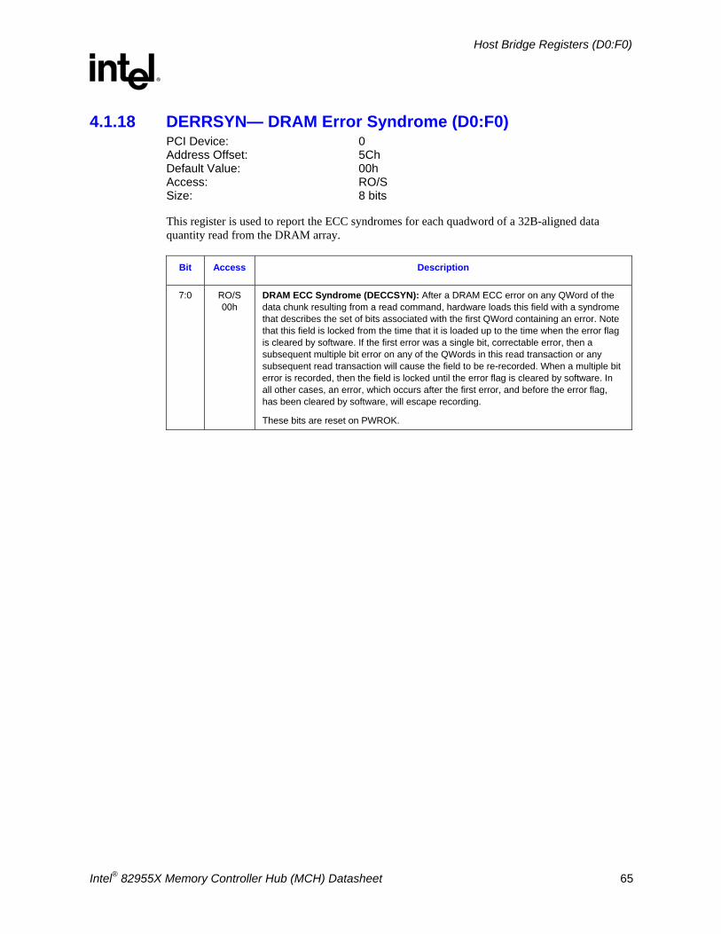
Host Bridge Registers (D0:F0)
R
Intel® 82955X Memory Controller Hub (MCH) Datasheet 65
4.1.18 DERRSYN— DRAM Error Syndrome (D0:F0) PCI Device: 0 Address Offset: 5Ch Default Value: 00h Access: RO/S Size: 8 bits
This register is used to report the ECC syndromes for each quadword of a 32B-aligned data quantity read from the DRAM array.
Bit Access Description
7:0 RO/S 00h
DRAM ECC Syndrome (DECCSYN): After a DRAM ECC error on any QWord of the data chunk resulting from a read command, hardware loads this field with a syndrome that describes the set of bits associated with the first QWord containing an error. Note that this field is locked from the time that it is loaded up to the time when the error flag is cleared by software. If the first error was a single bit, correctable error, then a subsequent multiple bit error on any of the QWords in this read transaction or any subsequent read transaction will cause the field to be re-recorded. When a multiple bit error is recorded, then the field is locked until the error flag is cleared by software. In all other cases, an error, which occurs after the first error, and before the error flag, has been cleared by software, will escape recording.
These bits are reset on PWROK.
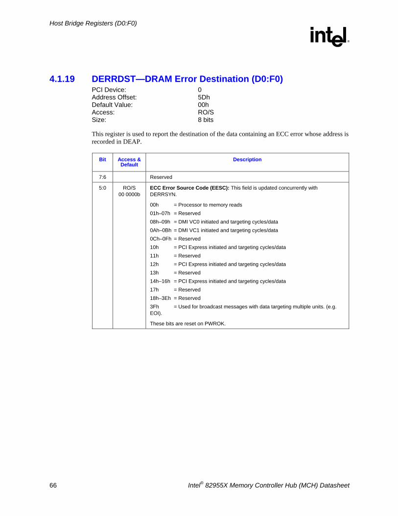
Host Bridge Registers (D0:F0)
R
66 Intel® 82955X Memory Controller Hub (MCH) Datasheet
4.1.19 DERRDST—DRAM Error Destination (D0:F0) PCI Device: 0 Address Offset: 5Dh Default Value: 00h Access: RO/S Size: 8 bits
This register is used to report the destination of the data containing an ECC error whose address is recorded in DEAP.
Bit Access & Default
Description
7:6 Reserved
5:0 RO/S 00 0000b
ECC Error Source Code (EESC): This field is updated concurrently with DERRSYN.
00h = Processor to memory reads 01h–07h = Reserved 08h–09h = DMI VC0 initiated and targeting cycles/data 0Ah–0Bh = DMI VC1 initiated and targeting cycles/data 0Ch–0Fh = Reserved 10h = PCI Express initiated and targeting cycles/data 11h = Reserved 12h = PCI Express initiated and targeting cycles/data 13h = Reserved 14h–16h = PCI Express initiated and targeting cycles/data 17h = Reserved 18h–3Eh = Reserved 3Fh = Used for broadcast messages with data targeting multiple units. (e.g. EOI).
These bits are reset on PWROK.
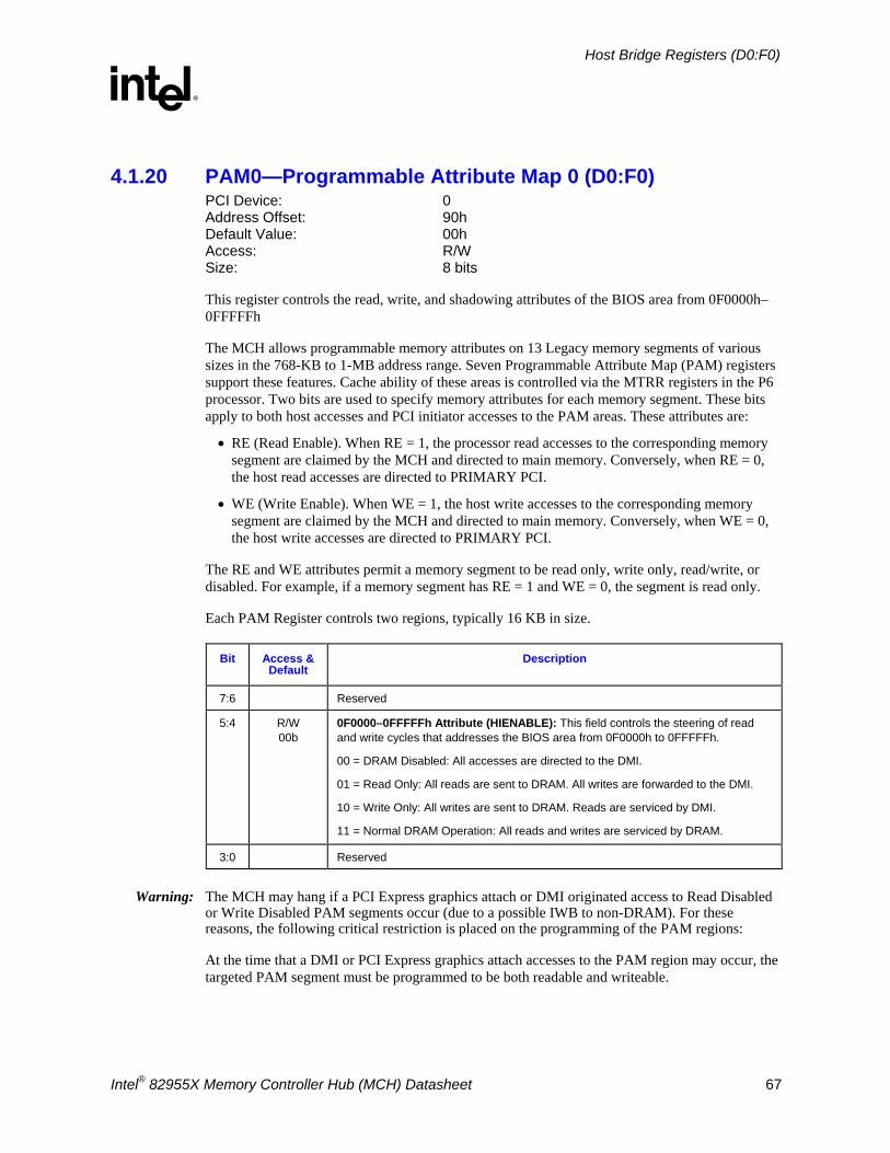
Host Bridge Registers (D0:F0)
R
Intel® 82955X Memory Controller Hub (MCH) Datasheet 67
4.1.20 PAM0—Programmable Attribute Map 0 (D0:F0) PCI Device: 0 Address Offset: 90h Default Value: 00h Access: R/W Size: 8 bits
This register controls the read, write, and shadowing attributes of the BIOS area from 0F0000h–0FFFFFh
The MCH allows programmable memory attributes on 13 Legacy memory segments of various sizes in the 768-KB to 1-MB address range. Seven Programmable Attribute Map (PAM) registers support these features. Cache ability of these areas is controlled via the MTRR registers in the P6 processor. Two bits are used to specify memory attributes for each memory segment. These bits apply to both host accesses and PCI initiator accesses to the PAM areas. These attributes are:
• RE (Read Enable). When RE = 1, the processor read accesses to the corresponding memory segment are claimed by the MCH and directed to main memory. Conversely, when RE = 0, the host read accesses are directed to PRIMARY PCI.
• WE (Write Enable). When WE = 1, the host write accesses to the corresponding memory segment are claimed by the MCH and directed to main memory. Conversely, when WE = 0, the host write accesses are directed to PRIMARY PCI.
The RE and WE attributes permit a memory segment to be read only, write only, read/write, or disabled. For example, if a memory segment has RE = 1 and WE = 0, the segment is read only.
Each PAM Register controls two regions, typically 16 KB in size.
Bit Access & Default
Description
7:6 Reserved
5:4 R/W 00b
0F0000–0FFFFFh Attribute (HIENABLE): This field controls the steering of read and write cycles that addresses the BIOS area from 0F0000h to 0FFFFFh.
00 = DRAM Disabled: All accesses are directed to the DMI.
01 = Read Only: All reads are sent to DRAM. All writes are forwarded to the DMI.
10 = Write Only: All writes are sent to DRAM. Reads are serviced by DMI.
11 = Normal DRAM Operation: All reads and writes are serviced by DRAM.
3:0 Reserved
Warning: The MCH may hang if a PCI Express graphics attach or DMI originated access to Read Disabled or Write Disabled PAM segments occur (due to a possible IWB to non-DRAM). For these reasons, the following critical restriction is placed on the programming of the PAM regions:
At the time that a DMI or PCI Express graphics attach accesses to the PAM region may occur, the targeted PAM segment must be programmed to be both readable and writeable.
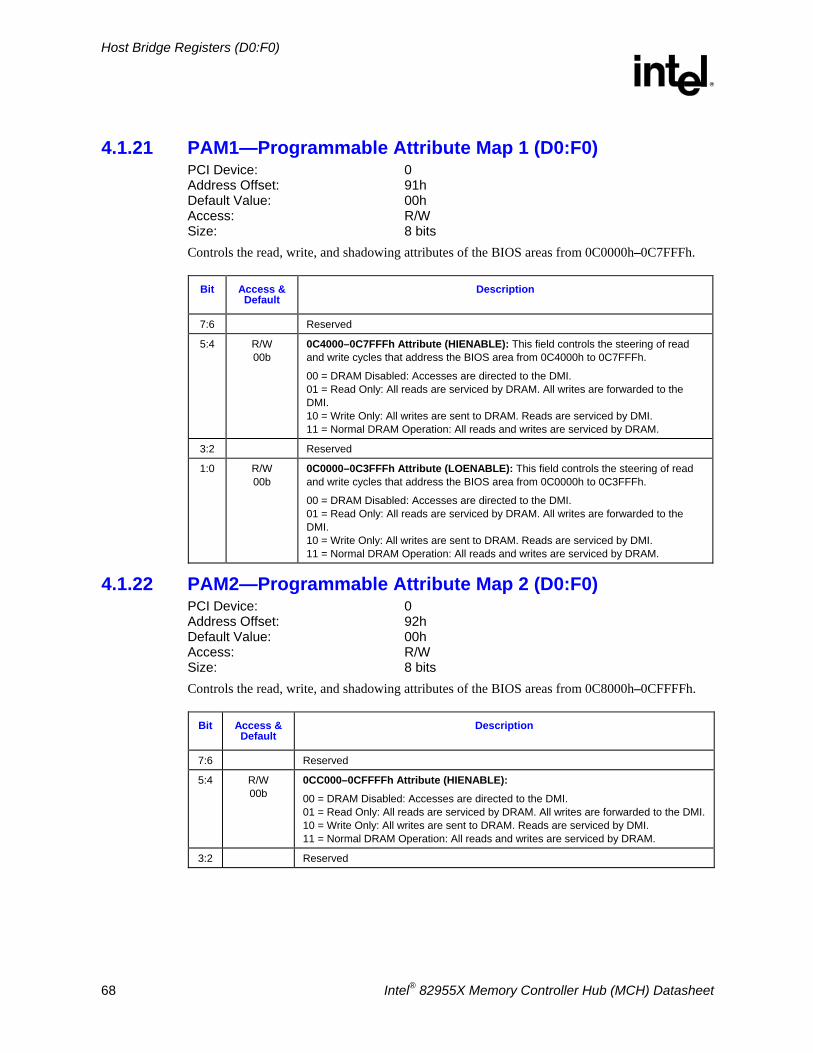
Host Bridge Registers (D0:F0)
R
68 Intel® 82955X Memory Controller Hub (MCH) Datasheet
4.1.21 PAM1—Programmable Attribute Map 1 (D0:F0) PCI Device: 0 Address Offset: 91h Default Value: 00h Access: R/W Size: 8 bits Controls the read, write, and shadowing attributes of the BIOS areas from 0C0000h–0C7FFFh.
Bit Access & Default
Description
7:6 Reserved
5:4 R/W 00b
0C4000–0C7FFFh Attribute (HIENABLE): This field controls the steering of read and write cycles that address the BIOS area from 0C4000h to 0C7FFFh.
00 = DRAM Disabled: Accesses are directed to the DMI. 01 = Read Only: All reads are serviced by DRAM. All writes are forwarded to the DMI. 10 = Write Only: All writes are sent to DRAM. Reads are serviced by DMI. 11 = Normal DRAM Operation: All reads and writes are serviced by DRAM.
3:2 Reserved
1:0 R/W 00b
0C0000–0C3FFFh Attribute (LOENABLE): This field controls the steering of read and write cycles that address the BIOS area from 0C0000h to 0C3FFFh.
00 = DRAM Disabled: Accesses are directed to the DMI. 01 = Read Only: All reads are serviced by DRAM. All writes are forwarded to the DMI. 10 = Write Only: All writes are sent to DRAM. Reads are serviced by DMI. 11 = Normal DRAM Operation: All reads and writes are serviced by DRAM.
4.1.22 PAM2—Programmable Attribute Map 2 (D0:F0) PCI Device: 0 Address Offset: 92h Default Value: 00h Access: R/W Size: 8 bits Controls the read, write, and shadowing attributes of the BIOS areas from 0C8000h–0CFFFFh.
Bit Access & Default
Description
7:6 Reserved
5:4 R/W 00b
0CC000–0CFFFFh Attribute (HIENABLE):
00 = DRAM Disabled: Accesses are directed to the DMI. 01 = Read Only: All reads are serviced by DRAM. All writes are forwarded to the DMI.10 = Write Only: All writes are sent to DRAM. Reads are serviced by DMI. 11 = Normal DRAM Operation: All reads and writes are serviced by DRAM.
3:2 Reserved
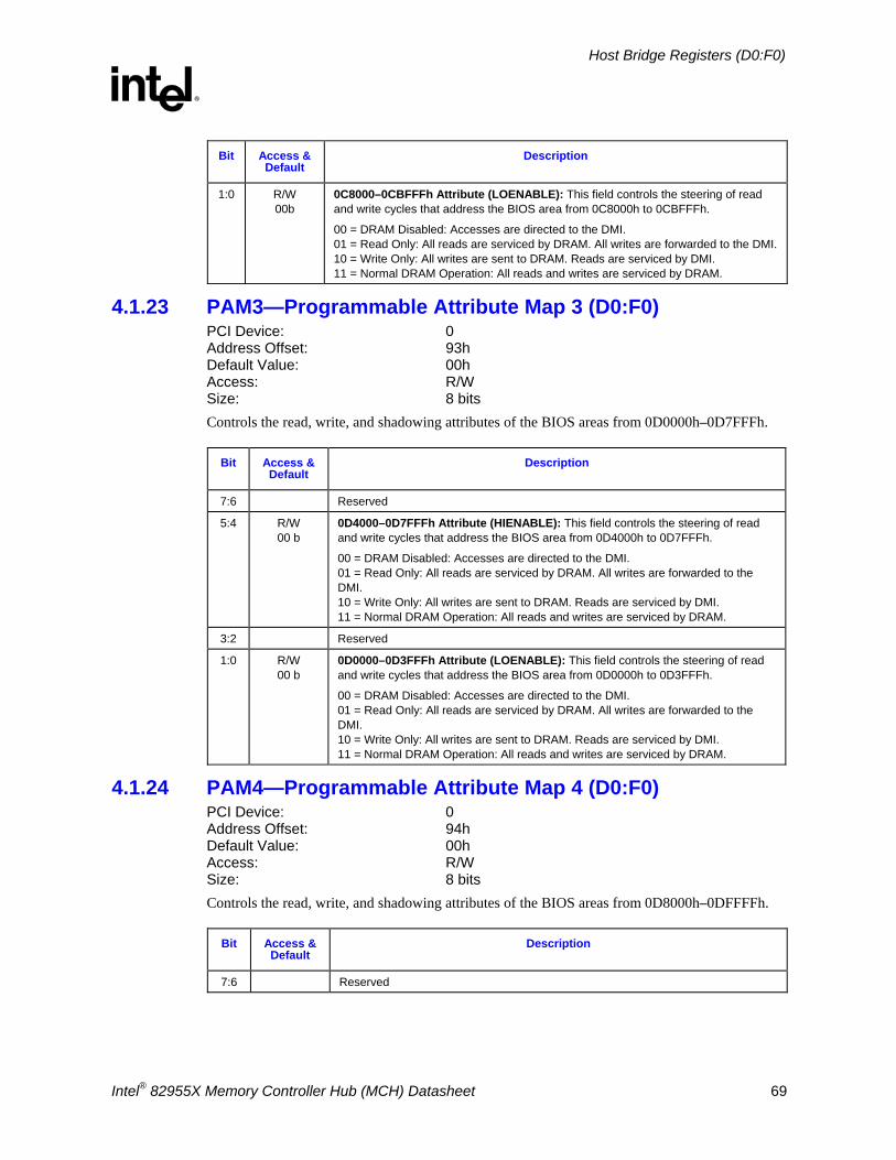
Host Bridge Registers (D0:F0)
R
Intel® 82955X Memory Controller Hub (MCH) Datasheet 69
Bit Access & Default
Description
1:0 R/W 00b
0C8000–0CBFFFh Attribute (LOENABLE): This field controls the steering of read and write cycles that address the BIOS area from 0C8000h to 0CBFFFh.
00 = DRAM Disabled: Accesses are directed to the DMI. 01 = Read Only: All reads are serviced by DRAM. All writes are forwarded to the DMI.10 = Write Only: All writes are sent to DRAM. Reads are serviced by DMI. 11 = Normal DRAM Operation: All reads and writes are serviced by DRAM.
4.1.23 PAM3—Programmable Attribute Map 3 (D0:F0) PCI Device: 0 Address Offset: 93h Default Value: 00h Access: R/W Size: 8 bits Controls the read, write, and shadowing attributes of the BIOS areas from 0D0000h–0D7FFFh.
Bit Access & Default
Description
7:6 Reserved
5:4 R/W 00 b
0D4000–0D7FFFh Attribute (HIENABLE): This field controls the steering of read and write cycles that address the BIOS area from 0D4000h to 0D7FFFh.
00 = DRAM Disabled: Accesses are directed to the DMI. 01 = Read Only: All reads are serviced by DRAM. All writes are forwarded to the DMI. 10 = Write Only: All writes are sent to DRAM. Reads are serviced by DMI. 11 = Normal DRAM Operation: All reads and writes are serviced by DRAM.
3:2 Reserved
1:0 R/W 00 b
0D0000–0D3FFFh Attribute (LOENABLE): This field controls the steering of read and write cycles that address the BIOS area from 0D0000h to 0D3FFFh.
00 = DRAM Disabled: Accesses are directed to the DMI. 01 = Read Only: All reads are serviced by DRAM. All writes are forwarded to the DMI. 10 = Write Only: All writes are sent to DRAM. Reads are serviced by DMI. 11 = Normal DRAM Operation: All reads and writes are serviced by DRAM.
4.1.24 PAM4—Programmable Attribute Map 4 (D0:F0) PCI Device: 0 Address Offset: 94h Default Value: 00h Access: R/W Size: 8 bits Controls the read, write, and shadowing attributes of the BIOS areas from 0D8000h–0DFFFFh.
Bit Access & Default
Description
7:6 Reserved
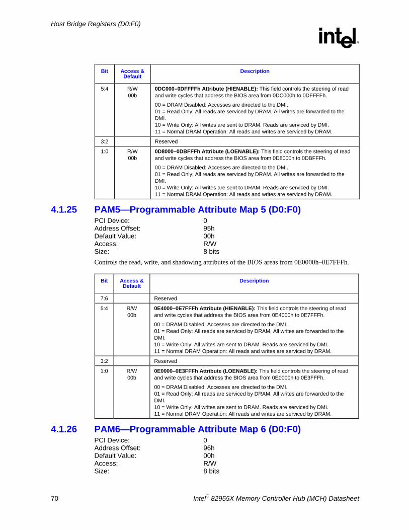
Host Bridge Registers (D0:F0)
R
70 Intel® 82955X Memory Controller Hub (MCH) Datasheet
Bit Access & Default
Description
5:4 R/W 00b
0DC000–0DFFFFh Attribute (HIENABLE): This field controls the steering of read and write cycles that address the BIOS area from 0DC000h to 0DFFFFh.
00 = DRAM Disabled: Accesses are directed to the DMI. 01 = Read Only: All reads are serviced by DRAM. All writes are forwarded to the DMI. 10 = Write Only: All writes are sent to DRAM. Reads are serviced by DMI. 11 = Normal DRAM Operation: All reads and writes are serviced by DRAM.
3:2 Reserved
1:0 R/W 00b
0D8000–0DBFFFh Attribute (LOENABLE): This field controls the steering of read and write cycles that address the BIOS area from 0D8000h to 0DBFFFh.
00 = DRAM Disabled: Accesses are directed to the DMI. 01 = Read Only: All reads are serviced by DRAM. All writes are forwarded to the DMI. 10 = Write Only: All writes are sent to DRAM. Reads are serviced by DMI. 11 = Normal DRAM Operation: All reads and writes are serviced by DRAM.
4.1.25 PAM5—Programmable Attribute Map 5 (D0:F0) PCI Device: 0 Address Offset: 95h Default Value: 00h Access: R/W Size: 8 bits Controls the read, write, and shadowing attributes of the BIOS areas from 0E0000h–0E7FFFh.
Bit Access & Default
Description
7:6 Reserved
5:4 R/W 00b
0E4000–0E7FFFh Attribute (HIENABLE): This field controls the steering of read and write cycles that address the BIOS area from 0E4000h to 0E7FFFh.
00 = DRAM Disabled: Accesses are directed to the DMI. 01 = Read Only: All reads are serviced by DRAM. All writes are forwarded to the DMI. 10 = Write Only: All writes are sent to DRAM. Reads are serviced by DMI. 11 = Normal DRAM Operation: All reads and writes are serviced by DRAM.
3:2 Reserved
1:0 R/W 00b
0E0000–0E3FFFh Attribute (LOENABLE): This field controls the steering of read and write cycles that address the BIOS area from 0E0000h to 0E3FFFh.
00 = DRAM Disabled: Accesses are directed to the DMI. 01 = Read Only: All reads are serviced by DRAM. All writes are forwarded to the DMI. 10 = Write Only: All writes are sent to DRAM. Reads are serviced by DMI. 11 = Normal DRAM Operation: All reads and writes are serviced by DRAM.
4.1.26 PAM6—Programmable Attribute Map 6 (D0:F0) PCI Device: 0 Address Offset: 96h Default Value: 00h Access: R/W Size: 8 bits
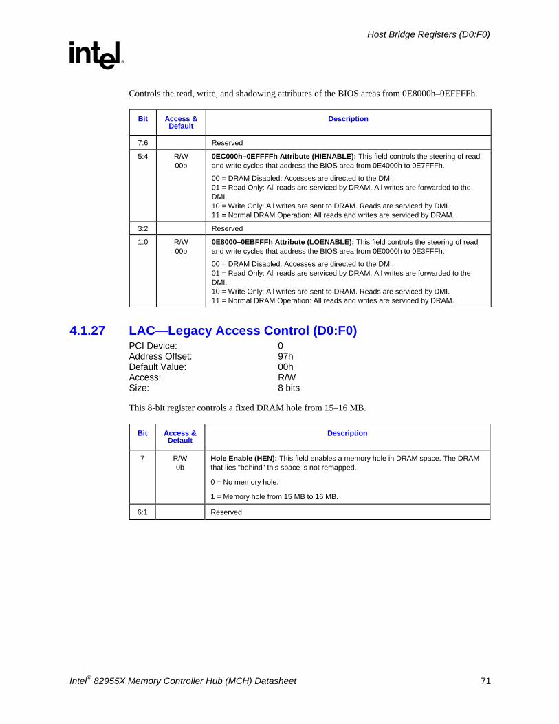
Host Bridge Registers (D0:F0)
R
Intel® 82955X Memory Controller Hub (MCH) Datasheet 71
Controls the read, write, and shadowing attributes of the BIOS areas from 0E8000h–0EFFFFh.
Bit Access & Default
Description
7:6 Reserved
5:4 R/W 00b
0EC000h–0EFFFFh Attribute (HIENABLE): This field controls the steering of read and write cycles that address the BIOS area from 0E4000h to 0E7FFFh.
00 = DRAM Disabled: Accesses are directed to the DMI. 01 = Read Only: All reads are serviced by DRAM. All writes are forwarded to the DMI. 10 = Write Only: All writes are sent to DRAM. Reads are serviced by DMI. 11 = Normal DRAM Operation: All reads and writes are serviced by DRAM.
3:2 Reserved
1:0 R/W 00b
0E8000–0EBFFFh Attribute (LOENABLE): This field controls the steering of read and write cycles that address the BIOS area from 0E0000h to 0E3FFFh.
00 = DRAM Disabled: Accesses are directed to the DMI. 01 = Read Only: All reads are serviced by DRAM. All writes are forwarded to the DMI. 10 = Write Only: All writes are sent to DRAM. Reads are serviced by DMI. 11 = Normal DRAM Operation: All reads and writes are serviced by DRAM.
4.1.27 LAC—Legacy Access Control (D0:F0) PCI Device: 0 Address Offset: 97h Default Value: 00h Access: R/W Size: 8 bits
This 8-bit register controls a fixed DRAM hole from 15–16 MB.
Bit Access & Default
Description
7 R/W 0b
Hole Enable (HEN): This field enables a memory hole in DRAM space. The DRAM that lies "behind" this space is not remapped.
0 = No memory hole.
1 = Memory hole from 15 MB to 16 MB.
6:1 Reserved
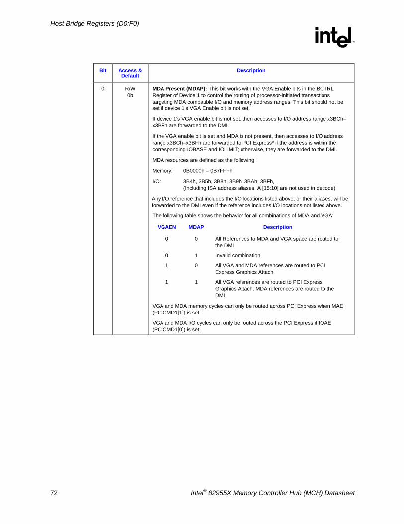
Host Bridge Registers (D0:F0)
R
72 Intel® 82955X Memory Controller Hub (MCH) Datasheet
Bit Access & Default
Description
0 R/W 0b
MDA Present (MDAP): This bit works with the VGA Enable bits in the BCTRL Register of Device 1 to control the routing of processor-initiated transactions targeting MDA compatible I/O and memory address ranges. This bit should not be set if device 1's VGA Enable bit is not set.
If device 1's VGA enable bit is not set, then accesses to I/O address range x3BCh–x3BFh are forwarded to the DMI.
If the VGA enable bit is set and MDA is not present, then accesses to I/O address range x3BCh–x3BFh are forwarded to PCI Express* if the address is within the corresponding IOBASE and IOLIMIT; otherwise, they are forwarded to the DMI.
MDA resources are defined as the following:
Memory: 0B0000h – 0B7FFFh
I/O: 3B4h, 3B5h, 3B8h, 3B9h, 3BAh, 3BFh, (Including ISA address aliases, A [15:10] are not used in decode)
Any I/O reference that includes the I/O locations listed above, or their aliases, will be forwarded to the DMI even if the reference includes I/O locations not listed above.
The following table shows the behavior for all combinations of MDA and VGA:
VGAEN MDAP Description
0 0 All References to MDA and VGA space are routed to the DMI
0 1 Invalid combination
1 0 All VGA and MDA references are routed to PCI Express Graphics Attach.
1 1 All VGA references are routed to PCI Express Graphics Attach. MDA references are routed to the DMI
VGA and MDA memory cycles can only be routed across PCI Express when MAE (PCICMD1[1]) is set.
VGA and MDA I/O cycles can only be routed across the PCI Express if IOAE (PCICMD1[0]) is set.
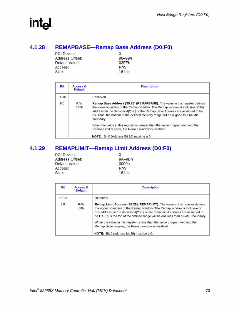
Host Bridge Registers (D0:F0)
R
Intel® 82955X Memory Controller Hub (MCH) Datasheet 73
4.1.28 REMAPBASE—Remap Base Address (D0:F0) PCI Device: 0 Address Offset: 98–99h Default Value: 03FFh Access: R/W Size: 16 bits
Bit Access &
Default Description
15:10 Reserved
9:0 R/W 3FFh
Remap Base Address [35:26] (REMAPBASE): The value in this register defines the lower boundary of the Remap window. The Remap window is inclusive of this address. In the decoder A[25:0] of the Remap Base Address are assumed to be 0s. Thus, the bottom of the defined memory range will be aligned to a 64 MB boundary.
When the value in this register is greater than the value programmed into the Remap Limit register, the Remap window is disabled.
NOTE: Bit 0 (Address Bit 26) must be a 0
4.1.29 REMAPLIMIT—Remap Limit Address (D0:F0) PCI Device: 0 Address Offset: 9A–9Bh Default Value: 0000h Access: R/W Size: 16 bits
Bit Access &
Default Description
15:10 Reserved
9:0 R/W 00h
Remap Limit Address [35:26] (REMAPLMT): The value in this register defines the upper boundary of the Remap window. The Remap window is inclusive of this address. In the decoder A[25:0] of the remap limit address are assumed to be F's. Thus the top of the defined range will be one less than a 64MB boundary.
When the value in this register is less than the value programmed into the Remap Base register, the Remap window is disabled.
NOTE: Bit 0 (address bit 26) must be a 0.
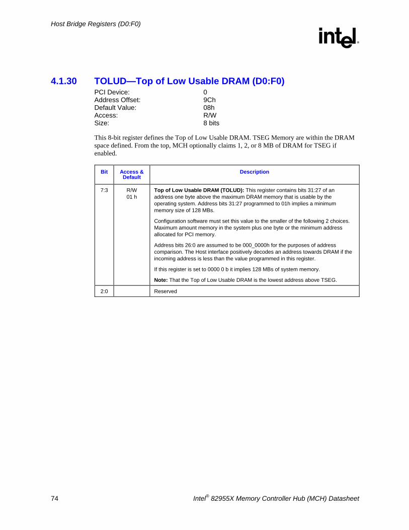
Host Bridge Registers (D0:F0)
R
74 Intel® 82955X Memory Controller Hub (MCH) Datasheet
4.1.30 TOLUD—Top of Low Usable DRAM (D0:F0) PCI Device: 0 Address Offset: 9Ch Default Value: 08h Access: R/W Size: 8 bits
This 8-bit register defines the Top of Low Usable DRAM. TSEG Memory are within the DRAM space defined. From the top, MCH optionally claims 1, 2, or 8 MB of DRAM for TSEG if enabled.
Bit Access & Default
Description
7:3 R/W 01 h
Top of Low Usable DRAM (TOLUD): This register contains bits 31:27 of an address one byte above the maximum DRAM memory that is usable by the operating system. Address bits 31:27 programmed to 01h implies a minimum memory size of 128 MBs.
Configuration software must set this value to the smaller of the following 2 choices. Maximum amount memory in the system plus one byte or the minimum address allocated for PCI memory.
Address bits 26:0 are assumed to be 000_0000h for the purposes of address comparison. The Host interface positively decodes an address towards DRAM if the incoming address is less than the value programmed in this register.
If this register is set to 0000 0 b it implies 128 MBs of system memory.
Note: That the Top of Low Usable DRAM is the lowest address above TSEG.
2:0 Reserved
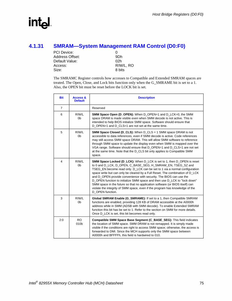
Host Bridge Registers (D0:F0)
R
Intel® 82955X Memory Controller Hub (MCH) Datasheet 75
4.1.31 SMRAM—System Management RAM Control (D0:F0) PCI Device: 0 Address Offset: 9Dh Default Value: 02h Access: R/W/L, RO Size: 8 bits
The SMRAMC Register controls how accesses to Compatible and Extended SMRAM spaces are treated. The Open, Close, and Lock bits function only when the G_SMRAME bit is set to a 1. Also, the OPEN bit must be reset before the LOCK bit is set.
Bit Access & Default
Description
7 Reserved
6 R/W/L 0b
SMM Space Open (D_OPEN): When D_OPEN=1 and D_LCK=0, the SMM space DRAM is made visible even when SMM decode is not active. This is intended to help BIOS initialize SMM space. Software should ensure that D_OPEN=1 and D_CLS=1 are not set at the same time.
5 R/W/L 0b
SMM Space Closed (D_CLS): When D_CLS = 1 SMM space DRAM is not accessible to data references, even if SMM decode is active. Code references may still access SMM space DRAM. This will allow SMM software to reference through SMM space to update the display even when SMM is mapped over the VGA range. Software should ensure that D_OPEN=1 and D_CLS=1 are not set at the same time. Note that the D_CLS bit only applies to Compatible SMM space.
4 R/W/L 0b
SMM Space Locked (D_LCK): When D_LCK is set to 1, then D_OPEN is reset to 0 and D_LCK, D_OPEN, C_BASE_SEG, H_SMRAM_EN, TSEG_SZ and TSEG_EN become read only. D_LCK can be set to 1 via a normal configuration space write but can only be cleared by a Full Reset. The combination of D_LCK and D_OPEN provide convenience with security. The BIOS can use the D_OPEN function to initialize SMM space and then use D_LCK to "lock down" SMM space in the future so that no application software (or BIOS itself) can violate the integrity of SMM space, even if the program has knowledge of the D_OPEN function.
3 R/W/L 0b
Global SMRAM Enable (G_SMRAME): If set to a 1, then Compatible SMRAM functions are enabled, providing 128 KB of DRAM accessible at the A0000h address while in SMM (ADSB with SMM decode). To enable Extended SMRAM function this bit has be set to 1. Refer to the section on SMM for more details. Once D_LCK is set, this bit becomes read only.
2:0 RO 010b
Compatible SMM Space Base Segment (C_BASE_SEG): This field indicates the location of SMM space. SMM DRAM is not remapped. It is simply made visible if the conditions are right to access SMM space; otherwise, the access is forwarded to DMI. Since the MCH supports only the SMM space between A0000h and BFFFFh, this field is hardwired to 010.
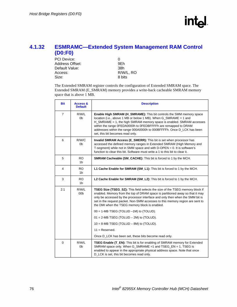
Host Bridge Registers (D0:F0)
R
76 Intel® 82955X Memory Controller Hub (MCH) Datasheet
4.1.32 ESMRAMC—Extended System Management RAM Control (D0:F0) PCI Device: 0 Address Offset: 9Eh Default Value: 38h Access: R/W/L, RO Size: 8 bits
The Extended SMRAM register controls the configuration of Extended SMRAM space. The Extended SMRAM (E_SMRAM) memory provides a write-back cacheable SMRAM memory space that is above 1 MB.
Bit Access & Default
Description
7 R/W/L 0b
Enable High SMRAM (H_SMRAME): This bit controls the SMM memory space location (i.e., above 1 MB or below 1 MB). When G_SMRAME = 1 and H_SMRAME = 1, the high SMRAM memory space is enabled. SMRAM accesses within the range 0FEDA0000h to 0FEDBFFFFh are remapped to DRAM addresses within the range 000A0000h to 000BFFFFh. Once D_LCK has been set, this bit becomes read only.
6 R/W/C 0b
Invalid SMRAM Access (E_SMERR): This bit is set when processor has accessed the defined memory ranges in Extended SMRAM (High Memory and T-segment) while not in SMM space and with D-OPEN = 0. It is software’s function to clear this bit. Software must write a 1 to this bit to clear it.
5 RO 1b
SMRAM Cacheable (SM_CACHE): This bit is forced to 1 by the MCH.
4 RO 1b
L1 Cache Enable for SMRAM (SM_L1): This bit is forced to 1 by the MCH.
3 RO 1b
L2 Cache Enable for SMRAM (SM_L2): This bit is forced to 1 by the MCH.
2:1 R/W/L 00b
TSEG Size (TSEG_SZ): This field selects the size of the TSEG memory block if enabled. Memory from the top of DRAM space is partitioned away so that it may only be accessed by the processor interface and only then when the SMM bit is set in the request packet. Non-SMM accesses to this memory region are sent to the DMI when the TSEG memory block is enabled.
00 = 1-MB TSEG (TOLUD –1M) to (TOLUD).
01 = 2-MB TSEG (TOLUD – 2M) to (TOLUD).
10 = 8-MB TSEG (TOLUD – 8M) to (TOLUD).
11 = Reserved.
Once D_LCK has been set, these bits become read only.
0 R/W/L 0b
TSEG Enable (T_EN): This bit is for enabling of SMRAM memory for Extended SMRAM space only. When G_SMRAME =1 and TSEG_EN = 1, TSEG is enabled to appear in the appropriate physical address space. Note that once D_LCK is set, this bit becomes read only.
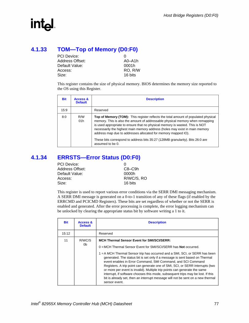
Host Bridge Registers (D0:F0)
R
Intel® 82955X Memory Controller Hub (MCH) Datasheet 77
4.1.33 TOM—Top of Memory (D0:F0) PCI Device: 0 Address Offset: A0–A1h Default Value: 0001h Access: RO, R/W Size: 16 bits
This register contains the size of physical memory. BIOS determines the memory size reported to the OS using this Register.
Bit Access & Default
Description
15:9 Reserved
8:0 R/W 01h
Top of Memory (TOM): This register reflects the total amount of populated physical memory. This is also the amount of addressable physical memory when remapping is used appropriate to ensure that no physical memory is wasted. This is NOT necessarily the highest main memory address (holes may exist in main memory address map due to addresses allocated for memory mapped IO).
These bits correspond to address bits 35:27 (128MB granularity). Bits 26:0 are assumed to be 0.
4.1.34 ERRSTS—Error Status (D0:F0) PCI Device: 0 Address Offset: C8–C9h Default Value: 0000h Access: R/WC/S, RO Size: 16 bits
This register is used to report various error conditions via the SERR DMI messaging mechanism. A SERR DMI message is generated on a 0-to-1 transition of any of these flags (if enabled by the ERRCMD and PCICMD Registers). These bits are set regardless of whether or not the SERR is enabled and generated. After the error processing is complete, the error logging mechanism can be unlocked by clearing the appropriate status bit by software writing a 1 to it.
Bit Access & Default
Description
15:12 Reserved
11 R/WC/S 0b
MCH Thermal Sensor Event for SMI/SCI/SERR:
0 = MCH Thermal Sensor Event for SMI/SCI/SERR has Not occurred.
1 = A MCH Thermal Sensor trip has occurred and a SMI, SCI, or SERR has been generated. The status bit is set only if a message is sent based on Thermal event enables in Error Command, SMI Command, and SCI Command Registers. A trip point can generate one of SMI, SCI, or SERR interrupts (two or more per event is invalid). Multiple trip points can generate the same interrupt, if software chooses this mode, subsequent trips may be lost. If this bit is already set, then an interrupt message will not be sent on a new thermal sensor event.
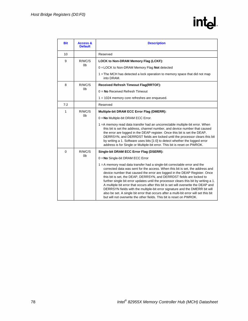
Host Bridge Registers (D0:F0)
R
78 Intel® 82955X Memory Controller Hub (MCH) Datasheet
Bit Access & Default
Description
10 Reserved
9 R/WC/S 0b
LOCK to Non-DRAM Memory Flag (LCKF):
0 = LOCK to Non-DRAM Memory Flag Not detected
1 = The MCH has detected a lock operation to memory space that did not map into DRAM.
8 R/WC/S 0b
Received Refresh Timeout Flag(RRTOF):
0 = No Received Refresh Timeout
1 = 1024 memory core refreshes are enqueued.
7:2 Reserved
1 R/WC/S 0b
Multiple-bit DRAM ECC Error Flag (DMERR):
0 = No Multiple-bit DRAM ECC Error.
1 =A memory read data transfer had an uncorrectable multiple-bit error. When this bit is set the address, channel number, and device number that caused the error are logged in the DEAP register. Once this bit is set the DEAP, DERRSYN, and DERRDST fields are locked until the processor clears this bit by writing a 1. Software uses bits [1:0] to detect whether the logged error address is for Single or Multiple-bit error. This bit is reset on PWROK.
0 R/WC/S 0b
Single-bit DRAM ECC Error Flag (DSERR):
0 = No Single-bit DRAM ECC Error
1 = A memory read data transfer had a single-bit correctable error and the corrected data was sent for the access. When this bit is set, the address and device number that caused the error are logged in the DEAP Register. Once this bit is set, the DEAP, DERRSYN, and DERRDST fields are locked to further single bit error updates until the processor clears this bit by writing a 1. A multiple bit error that occurs after this bit is set will overwrite the DEAP and DERRSYN fields with the multiple-bit error signature and the DMERR bit will also be set. A single bit error that occurs after a multi-bit error will set this bit but will not overwrite the other fields. This bit is reset on PWROK.
Host Bridge Registers (D0:F0)
R
Intel® 82955X Memory Controller Hub (MCH) Datasheet 79
4.1.35 ERRCMD—Error Command (D0:F0) PCI Device: 0 Address Offset: CA–CBh Default Value: 0000h Access: R/W Size: 16 bits
This register controls the MCH responses to various system errors. Since the MCH does not have an SERRB signal, SERR messages are passed from the MCH to the ICH7 over DMI. When a bit in this register is set, a SERR message will be generated on DMI whenever the corresponding flag is set in the ERRSTS register. The actual generation of the SERR message is globally enabled for Device 0 via the PCI Command Register.
Bit Access & Default
Description
15:12 Reserved
11 R/W 0b
SERR on MCH Thermal Sensor Event (TSESERR):
0 = Disable. Reporting of this condition via SERR messaging is disabled.
1 = The MCH generates a DMI SERR special cycle when bit 11 of the ERRSTS is set. The SERR must not be enabled at the same time as the SMI for the same thermal sensor event.
10 Reserved
9 R/W 0b
SERR on LOCK to non-DRAM Memory (LCKERR):
0 = Disable. Reporting of this condition via SERR messaging is disabled.
1 = The MCH will generate a DMI SERR special cycle whenever a processor lock cycle is detected that does not hit DRAM.
8 R/W 0b
SERR on DRAM Refresh Timeout (DRTOERR):
0 = Disable. Reporting of this condition via SERR messaging is disabled.
1 = The MCH generates a DMI SERR special cycle when a DRAM Refresh timeout occurs.
7:2 Reserved
1 R/W 0b
SERR Multiple-Bit DRAM ECC Error (DMERR):
0 = Disable. Reporting of this condition via SERR messaging is disabled. For systems not supporting ECC this bit must be disabled.
1 = The MCH generates an SERR message over DMI when it detects a multiple-bit error reported by the DRAM controller.
0 R/W 0b
SERR on Single-bit ECC Error (DSERR):
0 = Disable. Reporting of this condition via SERR messaging is disabled.
1 = The MCH generates an SERR special cycle over DMI when the DRAM controller detects a single bit error.
Host Bridge Registers (D0:F0)
R
80 Intel® 82955X Memory Controller Hub (MCH) Datasheet
4.1.36 SMICMD—SMI Command (D0:F0) PCI Device: 0 Address Offset: CC–CDh Default Value: 0000h Access: RO, R/W Size: 16 bits
This register enables various errors to generate an SMI DMI special cycle. When an error flag is set in the ERRSTS register, it can generate an SERR, SMI, or SCI DMI special cycle when enabled in the ERRCMD, SMICMD, or SCICMD registers, respectively. Note that one and only one message type can be enabled.
Bit Access Description
15:2 RO 000h
Reserved
1 R/W 0b
SMI on Multiple-Bit DRAM ECC Error (DMESMI):
0 = Disable. Reporting of this condition via SMI messaging is disabled. For systems not supporting ECC this bit must be disabled.
1 = The MCH generates an SMI DMI message when it detects a multiple-bit error reported by the DRAM controller.
0 R/W 0b
SMI on Single-bit ECC Error (DSESMI):
0 = Disable. Reporting of this condition via SMI messaging is disabled. For systems that do not support ECC this bit must be disabled.
1 = The MCH generates an SMI DMI special cycle when the DRAM controller detects a single bit error.
Host Bridge Registers (D0:F0)
R
Intel® 82955X Memory Controller Hub (MCH) Datasheet 81
4.1.37 SCICMD—SCI Command (D0:F0) PCI Device: 0 Address Offset: CE–CFh Default Value: 0000h Access: RO, R/W Size: 16 bits
This register enables various errors to generate an SMI DMI special cycle. When an error flag is set in the ERRSTS Register, it can generate an SERR, SMI, or SCI DMI special cycle when enabled in the ERRCMD, SMICMD, or SCICMD registers, respectively. Note that one and only one message type can be enabled.
Bit Access & Default
Description
15:2 RO 000h
Reserved
1 R/W 0b
SCI on Multiple-Bit DRAM ECC Error (DMESCI):
0 = Disable. Reporting of this condition via SCI messaging is disabled. For systems not supporting ECC this bit must be disabled.
1 = The MCH generates an SCI DMI message when it detects a multiple-bit error reported by the DRAM controller.
0 R/W 0b
SCI on Single-bit ECC Error (DSESCI):
0 = Disable. Reporting of this condition via SCI messaging is disabled. For systems that do not support ECC this bit must be disabled.
1 = The MCH generates an SCI DMI special cycle when the DRAM controller detects a single bit error.
4.1.38 SKPD—Scratchpad Data (D0:F0) PCI Device: 0 Address Offset: DC–DFh Default Value: 00000000h Access: R/W Size: 32 bits
This register holds 32 writable bits with no functionality. It is for the convenience of BIOS and graphics drivers.
Bit Access & Default
Description
31:0 R/W 00000000h
Scratchpad Data: 1 DWord of data storage.
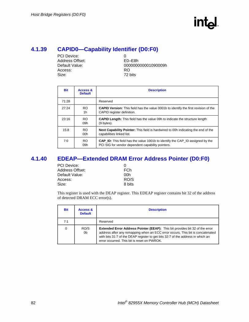
Host Bridge Registers (D0:F0)
R
82 Intel® 82955X Memory Controller Hub (MCH) Datasheet
4.1.39 CAPID0—Capability Identifier (D0:F0) PCI Device: 0 Address Offset: E0–E8h Default Value: 000000000001090009h Access: RO Size: 72 bits
Bit Access &
Default Description
71:28 Reserved
27:24 RO 1h
CAPID Version: This field has the value 0001b to identify the first revision of the CAPID register definition.
23:16 RO 09h
CAPID Length: This field has the value 09h to indicate the structure length (9 bytes).
15:8 RO 00h
Next Capability Pointer: This field is hardwired to 00h indicating the end of the capabilities linked list.
7:0 RO 09h
CAP_ID: This field has the value 1001b to identify the CAP_ID assigned by the PCI SIG for vendor dependent capability pointers.
4.1.40 EDEAP—Extended DRAM Error Address Pointer (D0:F0) PCI Device: 0 Address Offset: FCh Default Value: 00h Access: RO/S Size: 8 bits
This register is used with the DEAP register. This EDEAP register contains bit 32 of the address of detected DRAM ECC error(s).
Bit Access & Default
Description
7:1 Reserved
0 RO/S 0b
Extended Error Address Pointer (EEAP): This bit provides bit 32 of the error address after any remapping when an ECC error occurs. This bit is concatenated with bits 31:7 of the DEAP register to get bits 32:7 of the address in which an error occurred. This bit is reset on PWROK.
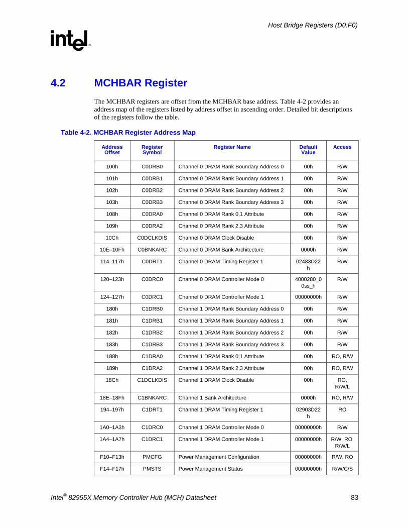
Host Bridge Registers (D0:F0)
R
Intel® 82955X Memory Controller Hub (MCH) Datasheet 83
4.2 MCHBAR Register The MCHBAR registers are offset from the MCHBAR base address. Table 4-2 provides an address map of the registers listed by address offset in ascending order. Detailed bit descriptions of the registers follow the table.
Table 4-2. MCHBAR Register Address Map
Address Offset
Register Symbol
Register Name Default Value
Access
100h C0DRB0 Channel 0 DRAM Rank Boundary Address 0 00h R/W
101h C0DRB1 Channel 0 DRAM Rank Boundary Address 1 00h R/W
102h C0DRB2 Channel 0 DRAM Rank Boundary Address 2 00h R/W
103h C0DRB3 Channel 0 DRAM Rank Boundary Address 3 00h R/W
108h C0DRA0 Channel 0 DRAM Rank 0,1 Attribute 00h R/W
109h C0DRA2 Channel 0 DRAM Rank 2,3 Attribute 00h R/W
10Ch C0DCLKDIS Channel 0 DRAM Clock Disable 00h R/W
10E–10Fh C0BNKARC Channel 0 DRAM Bank Architecture 0000h R/W
114–117h C0DRT1 Channel 0 DRAM Timing Register 1 02483D22h
R/W
120–123h C0DRC0 Channel 0 DRAM Controller Mode 0 4000280_00ss_h
R/W
124–127h C0DRC1 Channel 0 DRAM Controller Mode 1 00000000h R/W
180h C1DRB0 Channel 1 DRAM Rank Boundary Address 0 00h R/W
181h C1DRB1 Channel 1 DRAM Rank Boundary Address 1 00h R/W
182h C1DRB2 Channel 1 DRAM Rank Boundary Address 2 00h R/W
183h C1DRB3 Channel 1 DRAM Rank Boundary Address 3 00h R/W
188h C1DRA0 Channel 1 DRAM Rank 0,1 Attribute 00h RO, R/W
189h C1DRA2 Channel 1 DRAM Rank 2,3 Attribute 00h RO, R/W
18Ch C1DCLKDIS Channel 1 DRAM Clock Disable 00h RO, R/W/L
18E–18Fh C1BNKARC Channel 1 Bank Architecture 0000h RO, R/W
194–197h C1DRT1 Channel 1 DRAM Timing Register 1 02903D22h
RO
1A0–1A3h C1DRC0 Channel 1 DRAM Controller Mode 0 00000000h R/W
1A4–1A7h C1DRC1 Channel 1 DRAM Controller Mode 1 00000000h R/W, RO, R/W/L
F10–F13h PMCFG Power Management Configuration 00000000h R/W, RO
F14–F17h PMSTS Power Management Status 00000000h R/W/C/S
Host Bridge Registers (D0:F0)
R
84 Intel® 82955X Memory Controller Hub (MCH) Datasheet
4.2.1 C0DRB0—Channel A DRAM Rank Boundary Address 0 MMIO Range: MCHBAR Address Offset: 100h Default Value: 00h Access: R/W Size: 8 bits
The DRAM Rank Boundary Register defines the upper boundary address of each DRAM rank with a granularity of 32 MB. Each rank has its own single-byte DRB register. These registers are used to determine which chip select will be active for a given address.
Channel and rank map:
Channel A Rank 0: 100h Channel A Rank 1: 101h Channel A Rank 2: 102h Channel A Rank 3: 103h Channel B Rank 0: 180h Channel B Rank 1: 181h Channel B Rank 2: 182h Channel B Rank 3: 183h
Single Channel or Asymmetric Channels Example
If the channels are independent, addresses in Channel B should begin where addresses in Channel A left off, and the address of the first rank of Channel A can be calculated from the technology (256 Mbit, 512 Mbit, or 1 Gbit) and the x8 or x16 configuration. With independent channels a value of 01h in C0DRB0 indicates that 32 MB of DRAM has been populated in the first rank, and the top address in that rank is 32 MB.
Programming guide:
If Channel A is empty, all of the C0DRBs are programmed with 00h.
C0DRB0 = Total memory in chA rank0 (in 32-MB increments)
C0DRB1 = Total memory in chA rank0 + chA rank1 (in 32-MB increments)
––––
C1DRB0 = Total memory in chA rank0 + chA rank1 + chA rank2 + chA rank3 + chB rank0 (in 32-MB increments)
If Channel B is empty, all of the C1DRBs are programmed with the same value as C0DRB3.
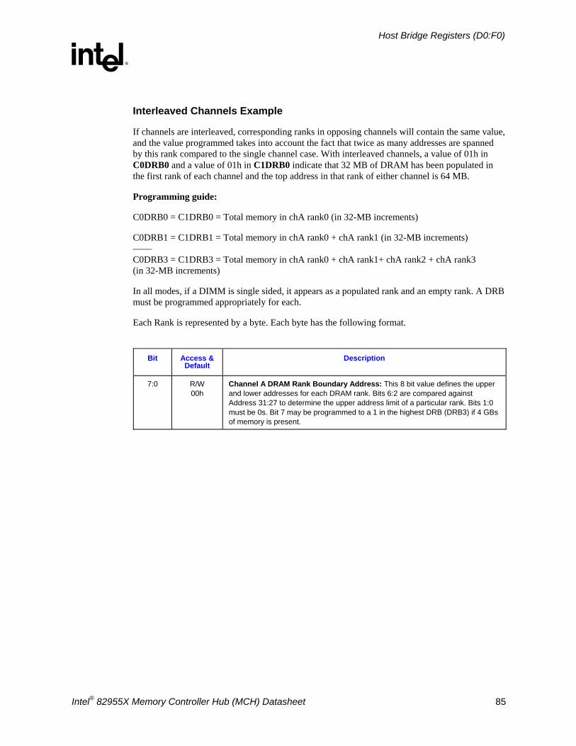
Host Bridge Registers (D0:F0)
R
Intel® 82955X Memory Controller Hub (MCH) Datasheet 85
Interleaved Channels Example
If channels are interleaved, corresponding ranks in opposing channels will contain the same value, and the value programmed takes into account the fact that twice as many addresses are spanned by this rank compared to the single channel case. With interleaved channels, a value of 01h in C0DRB0 and a value of 01h in C1DRB0 indicate that 32 MB of DRAM has been populated in the first rank of each channel and the top address in that rank of either channel is 64 MB.
Programming guide:
C0DRB0 = C1DRB0 = Total memory in chA rank0 (in 32-MB increments)
C0DRB1 = C1DRB1 = Total memory in chA rank0 + chA rank1 (in 32-MB increments) –––– C0DRB3 = C1DRB3 = Total memory in chA rank0 + chA rank1+ chA rank2 + chA rank3 (in 32-MB increments)
In all modes, if a DIMM is single sided, it appears as a populated rank and an empty rank. A DRB must be programmed appropriately for each.
Each Rank is represented by a byte. Each byte has the following format.
Bit Access &
Default Description
7:0 R/W 00h
Channel A DRAM Rank Boundary Address: This 8 bit value defines the upper and lower addresses for each DRAM rank. Bits 6:2 are compared against Address 31:27 to determine the upper address limit of a particular rank. Bits 1:0 must be 0s. Bit 7 may be programmed to a 1 in the highest DRB (DRB3) if 4 GBs of memory is present.
Host Bridge Registers (D0:F0)
R
86 Intel® 82955X Memory Controller Hub (MCH) Datasheet
4.2.2 C0DRB1—Channel A DRAM Rank Boundary Address 1 MMIO Range: MCHBAR Address Offset: 101h Default Value: 00h Access: R/W Size: 8 bits
The operation of this register is detailed in the description for the C0DRB0 Register.
4.2.3 C0DRB2—Channel A DRAM Rank Boundary Address 2 MMIO Range: MCHBAR Address Offset: 102h Default Value: 00h Access: R/W Size: 8 bits
The operation of this register is detailed in the description for the C0DRB0 Register.
4.2.4 C0DRB3—Channel A DRAM Rank Boundary Address 3 MMIO Range: MCHBAR Address Offset: 103h Default Value: 00h Access: R/W Size: 8 bits
The operation of this register is detailed in the description for the C0DRB0 Register.
Host Bridge Registers (D0:F0)
R
Intel® 82955X Memory Controller Hub (MCH) Datasheet 87
4.2.5 C0DRA0—Channel A DRAM Rank 0,1 Attribute MMIO Range: MCHBAR Address Offset: 108h Default Value: 00h Access: R/W Size: 8 bits
The DRAM Rank Attribute Registers define the page sizes to be used when accessing different ranks. These registers should be left with their default value (all zeros) for any rank that is unpopulated, as determined by the corresponding CxDRB Registers. Each byte of information in the CxDRA Registers describes the page size of a pair of ranks.
Channel and rank map:
Channel A Rank 0, 1: 108h Channel A Rank 2, 3: 109h Channel B Rank 0, 1: 188h Channel B Rank 2, 3: 189h
Bit Access &
Default Description
7 Reserved
6:4 R/W 000b
Channel A DRAM odd Rank Attribute: This 3 bit field defines the page size of the corresponding rank.
000 = Unpopulated 001 = Reserved 010 = 4 KB 011 = 8 KB 100 = 16 KB Others = Reserved
3 Reserved
2:0 R/W 000b
Channel A DRAM even Rank Attribute: This 3 bit field defines the page size of the corresponding rank.
000 = Unpopulated 001 = Reserved 010 = 4 KB 011 = 8 KB 100 = 16 KB Others = Reserved
4.2.6 C0DRA2—Channel A DRAM Rank 2, 3 Attribute MMIO Range: MCHBAR Address Offset: 109h Default Value: 00h Access: R/W Size: 8 bits
The operation of this register is detailed in the description for the C0DRA0 Register.
Host Bridge Registers (D0:F0)
R
88 Intel® 82955X Memory Controller Hub (MCH) Datasheet
4.2.7 C0DCLKDIS—Channel A DRAM Clock Disable MMIO Range: MCHBAR Address Offset: 10Ch Default Value: 00h Access: R/W Size: 8 bits
This register can be used to disable the system memory clock signals to each DIMM slot, which can significantly reduce EMI and Power concerns for clocks that go to unpopulated DIMMs. Clocks should be enabled based on whether a slot is populated, and what kind of DIMM is present.
Bit Access & Default
Description
7:6 Reserved
5 R/W 0b
DIMM Clock Gate Enable Pair 5:
0 = Tri-state the corresponding clock pair. 1 = Enable the corresponding clock pair.
4 R/W 0b
DIMM Clock Gate Enable Pair 4:
0 = Tri-state the corresponding clock pair. 1 = Enable the corresponding clock pair.
3 R/W 0b
DIMM Clock Gate Enable Pair 3:
0 = Tri-state the corresponding clock pair. 1 = Enable the corresponding clock pair.
2 R/W 0b
DIMM Clock Gate Enable Pair 2:
0 = Tri-state the corresponding clock pair. 1 = Enable the corresponding clock pair.
1 R/W 0b
DIMM Clock Gate Enable Pair 1:
0 = Tri-state the corresponding clock pair. 1 = Enable the corresponding clock pair.
0 R/W 0b
DIMM Clock Gate Enable Pair 0:
0 = Tri-state the corresponding clock pair. 1 = Enable the corresponding clock pair.
Note: Since there are multiple clock signals assigned to each Rank of a DIMM, it is important to clarify exactly which Rank width field affects which clock signal:
Channel Rank Clocks Affected
0 0 or 1 SCLK_A[2:0]/ SCLK_A[2:0]#
0 2 or 3 SCLK_A[5:3]/ SCLK_A[5:3]#
1 0 or 1 SCLK_B[2:0]/ SCLK_B[2:0]#
1 2 or 3 SCLK_B[5:3]/ SCLK_B[5:3]#
Host Bridge Registers (D0:F0)
R
Intel® 82955X Memory Controller Hub (MCH) Datasheet 89
4.2.8 C0BNKARC—Channel A DRAM Bank Architecture PCI Device: MCHBAR Function: 0 Address Offset: 10E–10Fh Default: 0000h Access: R/W Size: 16 bits
This register is used to program the bank architecture for each Rank.
Bit Access & Default
Description
15:8 Reserved
7:6 R/W 00b
Rank 3 Bank Architecture:
00 = 4 Bank.
01 = 8 Bank.
1X = Reserved
5:4 R/W 00b
Rank 2 Bank Architecture:
00 = 4 Bank.
01 = 8 Bank.
1X = Reserved
3:2 R/W 00b
Rank 1 Bank Architecture:
00 = 4 Bank.
01 = 8 Bank.
1X = Reserved
1:0 R/W 00b
Rank 0 Bank Architecture:
00 = 4 Bank.
01 = 8 Bank.
1X = Reserved
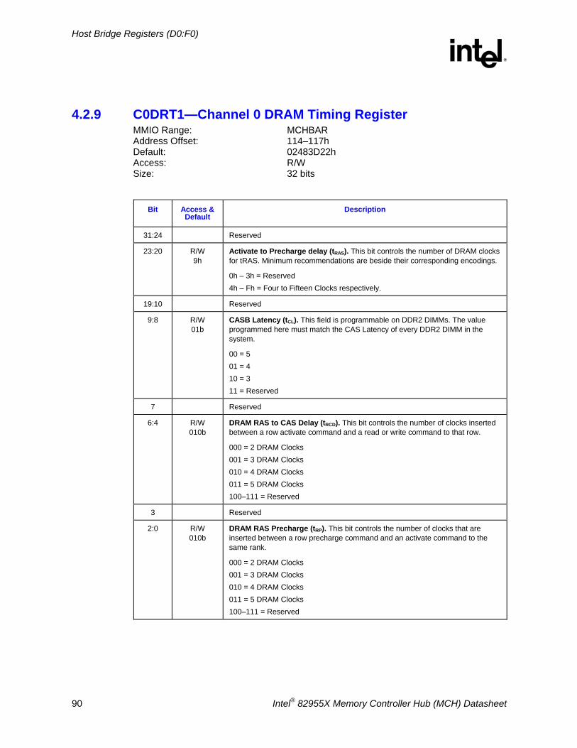
Host Bridge Registers (D0:F0)
R
90 Intel® 82955X Memory Controller Hub (MCH) Datasheet
4.2.9 C0DRT1—Channel 0 DRAM Timing Register MMIO Range: MCHBAR Address Offset: 114–117h Default: 02483D22h Access: R/W Size: 32 bits
Bit Access &
Default Description
31:24 Reserved
23:20 R/W 9h
Activate to Precharge delay (tRAS). This bit controls the number of DRAM clocks for tRAS. Minimum recommendations are beside their corresponding encodings.
0h – 3h = Reserved 4h – Fh = Four to Fifteen Clocks respectively.
19:10 Reserved
9:8 R/W 01b
CASB Latency (tCL). This field is programmable on DDR2 DIMMs. The value programmed here must match the CAS Latency of every DDR2 DIMM in the system.
00 = 5 01 = 4 10 = 3 11 = Reserved
7 Reserved
6:4 R/W 010b
DRAM RAS to CAS Delay (tRCD). This bit controls the number of clocks inserted between a row activate command and a read or write command to that row.
000 = 2 DRAM Clocks 001 = 3 DRAM Clocks 010 = 4 DRAM Clocks 011 = 5 DRAM Clocks 100–111 = Reserved
3 Reserved
2:0 R/W 010b
DRAM RAS Precharge (tRP). This bit controls the number of clocks that are inserted between a row precharge command and an activate command to the same rank.
000 = 2 DRAM Clocks 001 = 3 DRAM Clocks 010 = 4 DRAM Clocks 011 = 5 DRAM Clocks 100–111 = Reserved
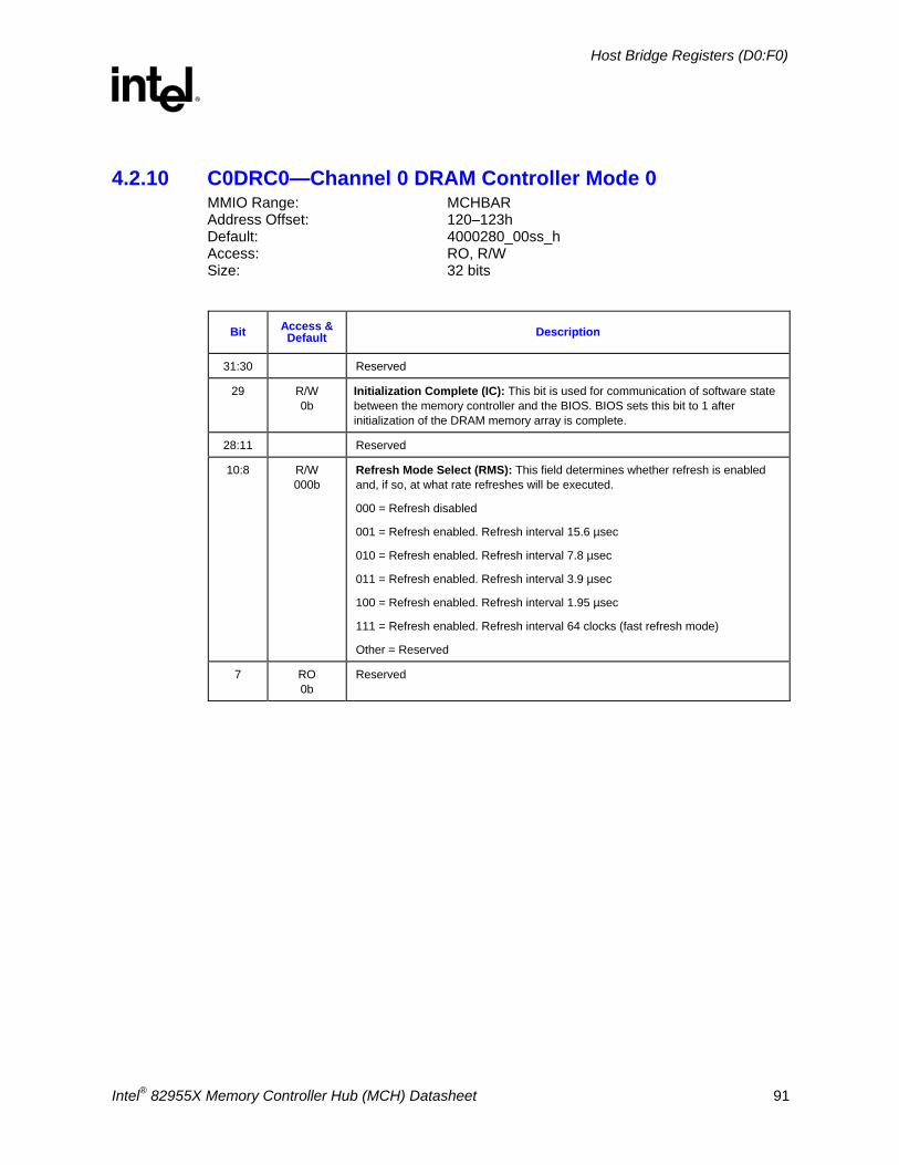
Host Bridge Registers (D0:F0)
R
Intel® 82955X Memory Controller Hub (MCH) Datasheet 91
4.2.10 C0DRC0—Channel 0 DRAM Controller Mode 0 MMIO Range: MCHBAR Address Offset: 120–123h Default: 4000280_00ss_h Access: RO, R/W Size: 32 bits
Bit Access & Default Description
31:30 Reserved
29 R/W 0b
Initialization Complete (IC): This bit is used for communication of software state between the memory controller and the BIOS. BIOS sets this bit to 1 after initialization of the DRAM memory array is complete.
28:11 Reserved
10:8 R/W 000b
Refresh Mode Select (RMS): This field determines whether refresh is enabled and, if so, at what rate refreshes will be executed.
000 = Refresh disabled
001 = Refresh enabled. Refresh interval 15.6 µsec
010 = Refresh enabled. Refresh interval 7.8 µsec
011 = Refresh enabled. Refresh interval 3.9 µsec
100 = Refresh enabled. Refresh interval 1.95 µsec
111 = Refresh enabled. Refresh interval 64 clocks (fast refresh mode)
Other = Reserved
7 RO 0b
Reserved
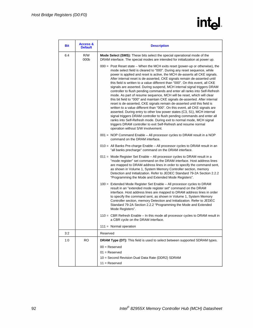
Host Bridge Registers (D0:F0)
R
92 Intel® 82955X Memory Controller Hub (MCH) Datasheet
Bit Access & Default Description
6:4 R/W 000b
Mode Select (SMS): These bits select the special operational mode of the DRAM interface. The special modes are intended for initialization at power up.
000 = Post Reset state – When the MCH exits reset (power-up or otherwise), the mode select field is cleared to "000". During any reset sequence, while power is applied and reset is active, the MCH de-asserts all CKE signals. After internal reset is de-asserted, CKE signals remain de-asserted until this field is written to a value different than "000". On this event, all CKE signals are asserted. During suspend, MCH internal signal triggers DRAM controller to flush pending commands and enter all ranks into Self-Refresh mode. As part of resume sequence, MCH will be reset, which will clear this bit field to "000" and maintain CKE signals de-asserted. After internal reset is de-asserted, CKE signals remain de-asserted until this field is written to a value different than "000". On this event, all CKE signals are asserted. During entry to other low power states (C3, S1), MCH internal signal triggers DRAM controller to flush pending commands and enter all ranks into Self-Refresh mode. During exit to normal mode, MCH signal triggers DRAM controller to exit Self-Refresh and resume normal operation without S/W involvement.
001 = NOP Command Enable – All processor cycles to DRAM result in a NOP command on the DRAM interface.
010 = All Banks Pre-charge Enable – All processor cycles to DRAM result in an "all banks precharge" command on the DRAM interface.
011 = Mode Register Set Enable – All processor cycles to DRAM result in a "mode register" set command on the DRAM interface. Host address lines are mapped to DRAM address lines in order to specify the command sent, as shown in Volume 1, System Memory Controller section, memory Detection and Initialization. Refer to JEDEC Standard 79-2A Section 2.2.2 “Programming the Mode and Extended Mode Registers”.
100 = Extended Mode Register Set Enable – All processor cycles to DRAM result in an "extended mode register set" command on the DRAM interface. Host address lines are mapped to DRAM address lines in order to specify the command sent, as shown in Volume 1, System Memory Controller section, memory Detection and Initialization. Refer to JEDEC Standard 79-2A Section 2.2.2 “Programming the Mode and Extended Mode Registers”.
110 = CBR Refresh Enable – In this mode all processor cycles to DRAM result in a CBR cycle on the DRAM interface.
111 = Normal operation
3:2 Reserved
1:0 RO DRAM Type (DT): This field is used to select between supported SDRAM types.
00 = Reserved 01 = Reserved 10 = Second Revision Dual Data Rate (DDR2) SDRAM 11 = Reserved
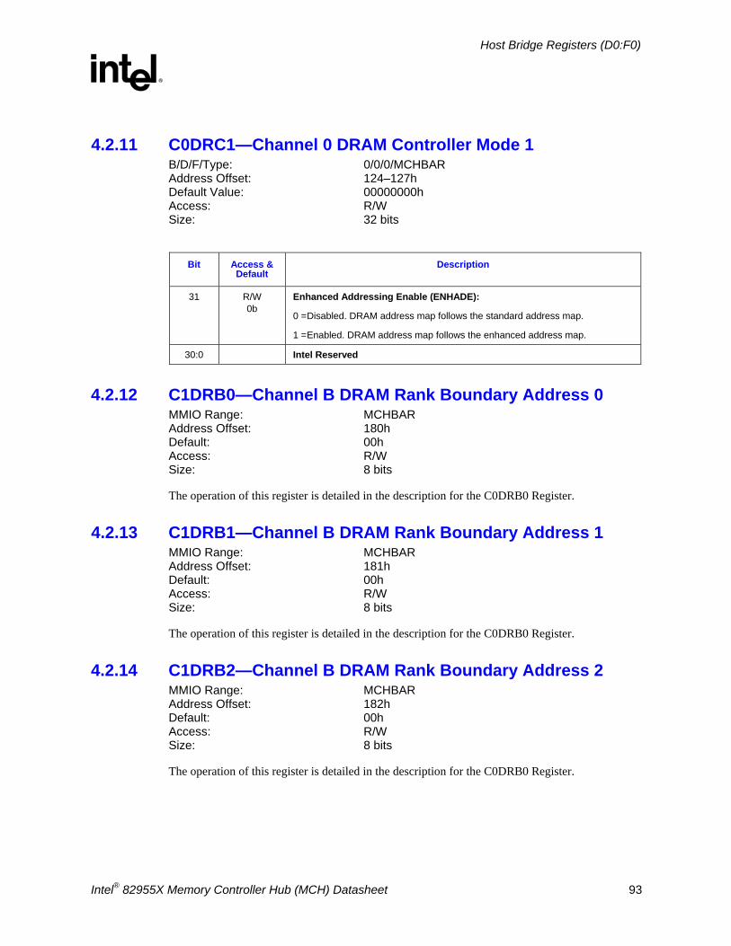
Host Bridge Registers (D0:F0)
R
Intel® 82955X Memory Controller Hub (MCH) Datasheet 93
4.2.11 C0DRC1—Channel 0 DRAM Controller Mode 1 B/D/F/Type: 0/0/0/MCHBAR Address Offset: 124–127h Default Value: 00000000h Access: R/W Size: 32 bits
Bit Access &
Default Description
31 R/W 0b
Enhanced Addressing Enable (ENHADE):
0 = Disabled. DRAM address map follows the standard address map.
1 = Enabled. DRAM address map follows the enhanced address map.
30:0 Intel Reserved
4.2.12 C1DRB0—Channel B DRAM Rank Boundary Address 0 MMIO Range: MCHBAR Address Offset: 180h Default: 00h Access: R/W Size: 8 bits
The operation of this register is detailed in the description for the C0DRB0 Register.
4.2.13 C1DRB1—Channel B DRAM Rank Boundary Address 1 MMIO Range: MCHBAR Address Offset: 181h Default: 00h Access: R/W Size: 8 bits
The operation of this register is detailed in the description for the C0DRB0 Register.
4.2.14 C1DRB2—Channel B DRAM Rank Boundary Address 2 MMIO Range: MCHBAR Address Offset: 182h Default: 00h Access: R/W Size: 8 bits
The operation of this register is detailed in the description for the C0DRB0 Register.
Host Bridge Registers (D0:F0)
R
94 Intel® 82955X Memory Controller Hub (MCH) Datasheet
4.2.15 C1DRB3—Channel B DRAM Rank Boundary Address 3 MMIO Range: MCHBAR Address Offset: 183h Default: 00h Access: R/W Size: 8 bits
The operation of this register is detailed in the description for the C0DRB0 Register.
4.2.16 C1DRA0—Channel B DRAM Rank 0,1 Attribute MMIO Range: MCHBAR Address Offset: 188h Default: 00h Access: R/W Size: 8 bits
The operation of this register is detailed in the description for the C0DRA0 Register.
4.2.17 C1DRA2—Channel B DRAM Rank 2,3 Attribute MMIO Range: MCHBAR Address Offset: 189h Default: 00h Access: R/W Size: 8 bits
The operation of this register is detailed in the description for the C0DRA0 Register.
4.2.18 C1DCLKDIS—Channel B DRAM Clock Disable MMIO Range: MCHBAR Address Offset: 18Ch Default: 00h Access: R/W/L Size: 8 bits
The operation of this register is detailed in the description for the C0DCLKDIS Register.
Host Bridge Registers (D0:F0)
R
Intel® 82955X Memory Controller Hub (MCH) Datasheet 95
4.2.19 C1BNKARC—Channel B Bank Architecture MMIO Range: MCHBAR Address Offset: 18E–18Fh Default: 0000h Access: R/W Size: 16 bits
The operation of this register is detailed in the description for the C0BNKARC Register.
4.2.20 C1DRT1—Channel 1 DRAM Timing Register 1 MMIO Range: MCHBAR Address Offset: 194–197h Default: 02483D22h Access: R/W Size: 32 bits
The operation of this register is detailed in the description for the C0DRT1 Register.
4.2.21 C1DRC0—Channel 1 DRAM Controller Mode 0 MMIO Range: MCHBAR Address Offset: 1A0–1A3h Default: 4000280_00??h Access: R/W Size: 32 bits
The operation of this register is detailed in the description for the C0DRC0 Register.
4.2.22 C1DRC1—Channel 1 DRAM Controller Mode 1 MMIO Range: MCHBAR Address Offset: 1A4–1A7h Default: 00000000h Access: RO, R/W, R/W/L Size: 32 bits
The operation of this register is detailed in the description for the C0DRC1 Register.
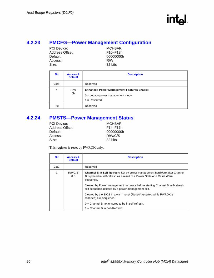
Host Bridge Registers (D0:F0)
R
96 Intel® 82955X Memory Controller Hub (MCH) Datasheet
4.2.23 PMCFG—Power Management Configuration PCI Device: MCHBAR Address Offset: F10–F13h Default: 00000000h Access: R/W Size: 32 bits
Bit Access & Default
Description
31:5 Reserved
4 R/W 0b
Enhanced Power Management Features Enable:
0 = Legacy power management mode 1 = Reserved.
3:0 Reserved
4.2.24 PMSTS—Power Management Status PCI Device: MCHBAR Address Offset: F14–F17h Default: 00000000h Access: R/W/C/S Size: 32 bits
This register is reset by PWROK only.
Bit Access & Default
Description
31:2 Reserved
1 R/WC/S 0 b
Channel B in Self-Refresh: Set by power management hardware after Channel B is placed in self-refresh as a result of a Power State or a Reset Warn sequence.
Cleared by Power management hardware before starting Channel B self-refresh exit sequence initiated by a power management exit.
Cleared by the BIOS in a warm reset (Reset# asserted while PWROK is asserted) exit sequence.
0 = Channel B not ensured to be in self-refresh. 1 = Channel B in Self-Refresh.
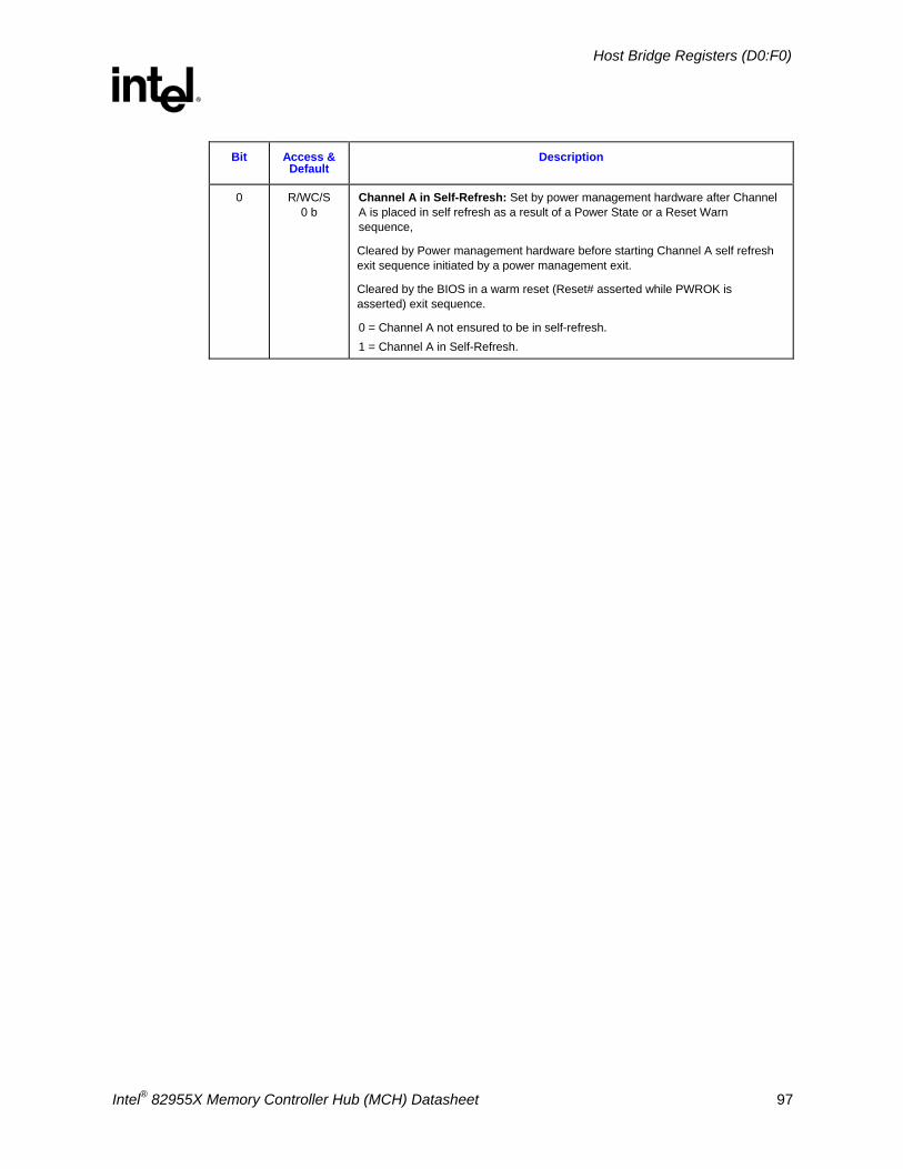
Host Bridge Registers (D0:F0)
R
Intel® 82955X Memory Controller Hub (MCH) Datasheet 97
Bit Access & Default
Description
0 R/WC/S 0 b
Channel A in Self-Refresh: Set by power management hardware after Channel A is placed in self refresh as a result of a Power State or a Reset Warn sequence,
Cleared by Power management hardware before starting Channel A self refresh exit sequence initiated by a power management exit.
Cleared by the BIOS in a warm reset (Reset# asserted while PWROK is asserted) exit sequence.
0 = Channel A not ensured to be in self-refresh. 1 = Channel A in Self-Refresh.
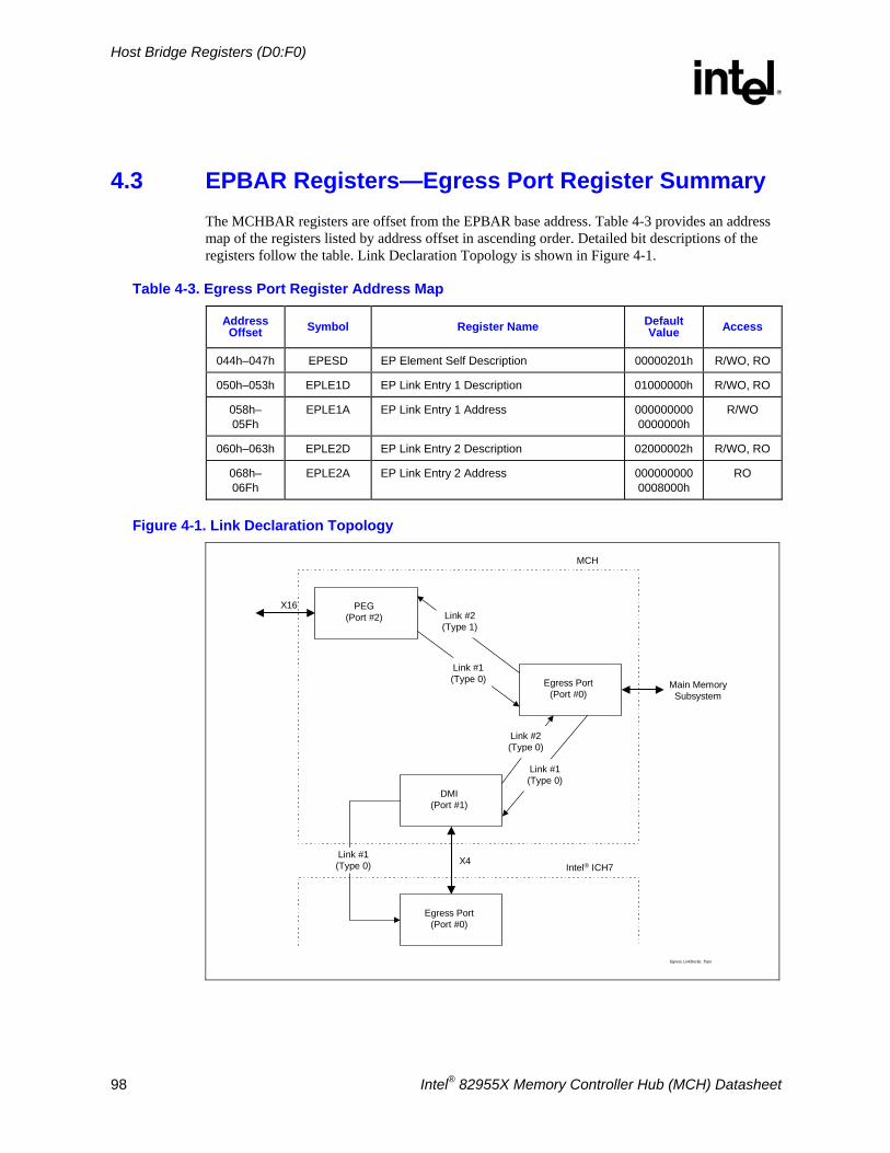
Host Bridge Registers (D0:F0)
R
98 Intel® 82955X Memory Controller Hub (MCH) Datasheet
4.3 EPBAR Registers—Egress Port Register Summary The MCHBAR registers are offset from the EPBAR base address. Table 4-3 provides an address map of the registers listed by address offset in ascending order. Detailed bit descriptions of the registers follow the table. Link Declaration Topology is shown in Figure 4-1.
Table 4-3. Egress Port Register Address Map
Address Offset Symbol Register Name Default
Value Access
044h–047h EPESD EP Element Self Description 00000201h R/WO, RO
050h–053h EPLE1D EP Link Entry 1 Description 01000000h R/WO, RO
058h–05Fh
EPLE1A EP Link Entry 1 Address 0000000000000000h
R/WO
060h–063h EPLE2D EP Link Entry 2 Description 02000002h R/WO, RO
068h–06Fh
EPLE2A EP Link Entry 2 Address 0000000000008000h
RO
Figure 4-1. Link Declaration Topology
PEG(Port #2)
Egress_LinkDeclar_Topo
Egress Port(Port #0)
DMI(Port #1)
Link #2(Type 1)
Link #1(Type 0)
Link #2(Type 0)
Link #1(Type 0)
Egress Port(Port #0)
X4
X16
MCH
Main MemorySubsystem
Intel® ICH7Link #1(Type 0)
Host Bridge Registers (D0:F0)
R
Intel® 82955X Memory Controller Hub (MCH) Datasheet 99
4.3.1 EPESD—EP Element Self Description MMIO Range: EPBAR Address Offset: 044–047h Default Value: 00000201h Access: RO, R/WO Size: 32 bits
This register provides information about the root complex element containing this Link Declaration Capability.
Bit Access & Default
Description
31:24 RO 00h
Port Number: This field specifies the port number associated with this element with respect to the component that contains this element.
Value of 00 h indicates to configuration software that this is the default egress port.
23:16 R/WO 00h
Component ID: This field identifies the physical component that contains this Root Complex Element. Component IDs start at 1.
This value is a mirror of the value in the Component ID field of all elements in this component. The value only needs to be written in one of the mirrored fields and it will be reflected everywhere that it is mirrored.
15:8 RO 02h
Number of Link Entries: This field indicates the number of link entries following the Element Self Description. This field reports 2 (one each for PCI Express and DMI).
7:4 Reserved
3:0 RO 01h
Element Type: This field indicates the type of the Root Complex Element. Value of 1h represents a port to system memory
Host Bridge Registers (D0:F0)
R
100 Intel® 82955X Memory Controller Hub (MCH) Datasheet
4.3.2 EPLE1D—EP Link Entry 1 Description MMIO Range: EPBAR Address Offset: 050–053h Default Value: 01000000h Access: RO, R/WO Size: 32 bits
This register provides the first part of a Link Entry that declares an internal link to another Root Complex Element.
Bit Access & Default
Description
31:24 RO 01h
Target Port Number: This field specifies the port number associated with the element targeted by this link entry (DMI). The target port number is with respect to the component that contains this element as specified by the target component ID.
23:16 R/WO 00h
Target Component ID: This field identifies the physical or logical component that is targeted by this link entry. A value of 0 is reserved; Component IDs start at 1.
This value is a mirror of the value in the Component ID field of all elements in this component. The value only needs to be written in one of the mirrored fields and it will be reflected everywhere that it is mirrored.
15:2 Reserved
1 RO 0b
Link Type: This field indicates that the link points to memory-mapped space (for RCRB). The link address specifies the 64-bit base address of the target RCRB.
0 R/WO 0b
Link Valid:
0 = Link Entry is not valid and will be ignored.
1 = Link Entry specifies a valid link.
Host Bridge Registers (D0:F0)
R
Intel® 82955X Memory Controller Hub (MCH) Datasheet 101
4.3.3 EPLE1A—EP Link Entry 1 Address MMIO Range: EPBAR Address Offset: 058–05Fh Default Value: 00000000_00000000h Access: R/WO Size: 64 bits
This register provides the second part of a Link Entry that declares an internal link to another Root Complex Element.
Bit Access & Default
Description
63:32 Reserved
31:12 R/WO
0 0000 h
Link Address: This field provides the memory mapped base address of the RCRB that is the target element (DMI) for this link entry.
11:0 Reserved
4.3.4 EPLE2D—EP Link Entry 2 Description MMIO Range: EPBAR Address Offset: 060–063h Default Value: 00000000h Access: RO, R/WO Size: 32 bits
This register provides the first part of a Link Entry that declares an internal link to another Root Complex Element.
Bit Access & Default
Description
31:24 RO 02h
Target Port Number: This field specifies the port number associated with the element targeted by this link entry (PCI Express). The target port number is with respect to the component that contains this element as specified by the target component ID.
23:16 R/WO 00h
Target Component ID: This field identifies the physical or logical component that is targeted by this link entry. A value of 0 is reserved; Component IDs start at 1.
This value is a mirror of the value in the Component ID field of all elements in this component. The value only needs to be written in one of the mirrored fields and it will be reflected everywhere that it is mirrored.
15:2 Reserved
1 RO 1b
Link Type: This field indicates that the link points to configuration space of the integrated device that controls the x16 root port. The link address specifies the configuration address (segment, bus, device, function) of the target root port.
0 R/WO 0b
Link Valid:
0 = Link Entry is not valid and will be ignored. 1 = Link Entry specifies a valid link.
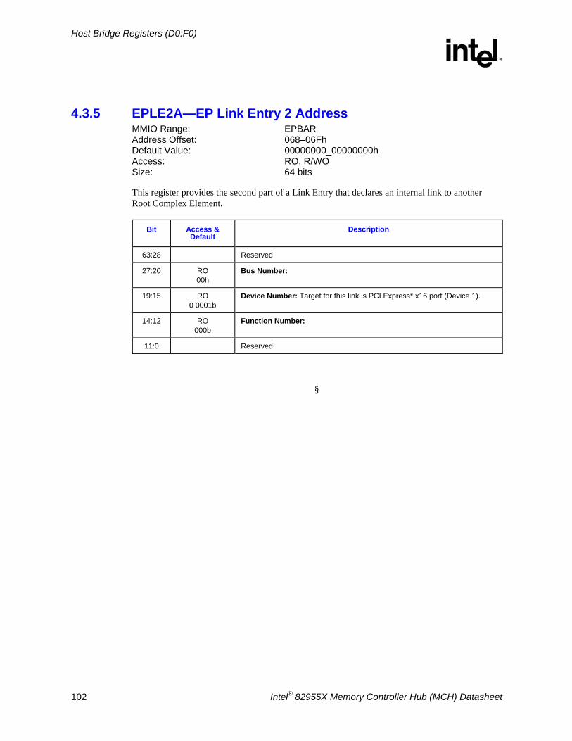
Host Bridge Registers (D0:F0)
R
102 Intel® 82955X Memory Controller Hub (MCH) Datasheet
4.3.5 EPLE2A—EP Link Entry 2 Address MMIO Range: EPBAR Address Offset: 068–06Fh Default Value: 00000000_00000000h Access: RO, R/WO Size: 64 bits
This register provides the second part of a Link Entry that declares an internal link to another Root Complex Element.
Bit Access & Default
Description
63:28 Reserved
27:20 RO 00h
Bus Number:
19:15 RO 0 0001b
Device Number: Target for this link is PCI Express* x16 port (Device 1).
14:12 RO 000b
Function Number:
11:0 Reserved
§
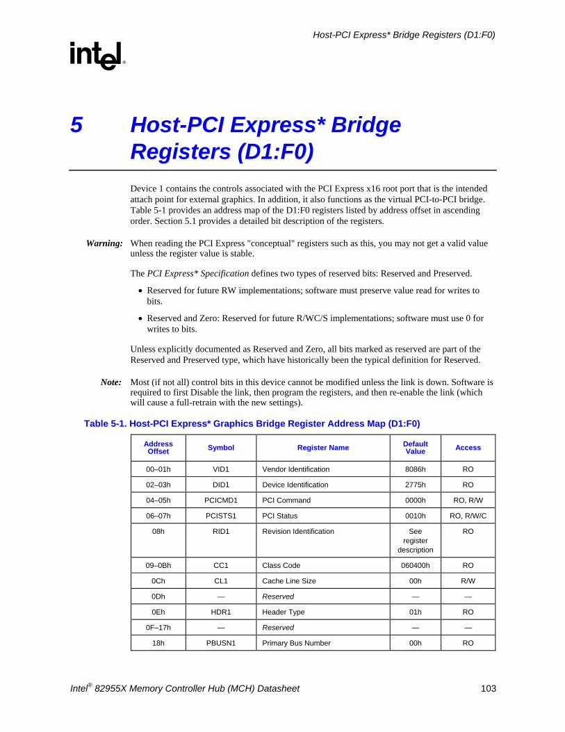
Host-PCI Express* Bridge Registers (D1:F0)
R
Intel® 82955X Memory Controller Hub (MCH) Datasheet 103
5 Host-PCI Express* Bridge Registers (D1:F0) Device 1 contains the controls associated with the PCI Express x16 root port that is the intended attach point for external graphics. In addition, it also functions as the virtual PCI-to-PCI bridge. Table 5-1 provides an address map of the D1:F0 registers listed by address offset in ascending order. Section 5.1 provides a detailed bit description of the registers.
Warning: When reading the PCI Express "conceptual" registers such as this, you may not get a valid value unless the register value is stable.
The PCI Express* Specification defines two types of reserved bits: Reserved and Preserved.
• Reserved for future RW implementations; software must preserve value read for writes to bits.
• Reserved and Zero: Reserved for future R/WC/S implementations; software must use 0 for writes to bits.
Unless explicitly documented as Reserved and Zero, all bits marked as reserved are part of the Reserved and Preserved type, which have historically been the typical definition for Reserved.
Note: Most (if not all) control bits in this device cannot be modified unless the link is down. Software is required to first Disable the link, then program the registers, and then re-enable the link (which will cause a full-retrain with the new settings).
Table 5-1. Host-PCI Express* Graphics Bridge Register Address Map (D1:F0)
Address Offset Symbol Register Name Default
Value Access
00–01h VID1 Vendor Identification 8086h RO
02–03h DID1 Device Identification 2775h RO
04–05h PCICMD1 PCI Command 0000h RO, R/W
06–07h PCISTS1 PCI Status 0010h RO, R/W/C
08h RID1 Revision Identification See register
description
RO
09–0Bh CC1 Class Code 060400h RO
0Ch CL1 Cache Line Size 00h R/W
0Dh — Reserved — —
0Eh HDR1 Header Type 01h RO
0F–17h — Reserved — —
18h PBUSN1 Primary Bus Number 00h RO
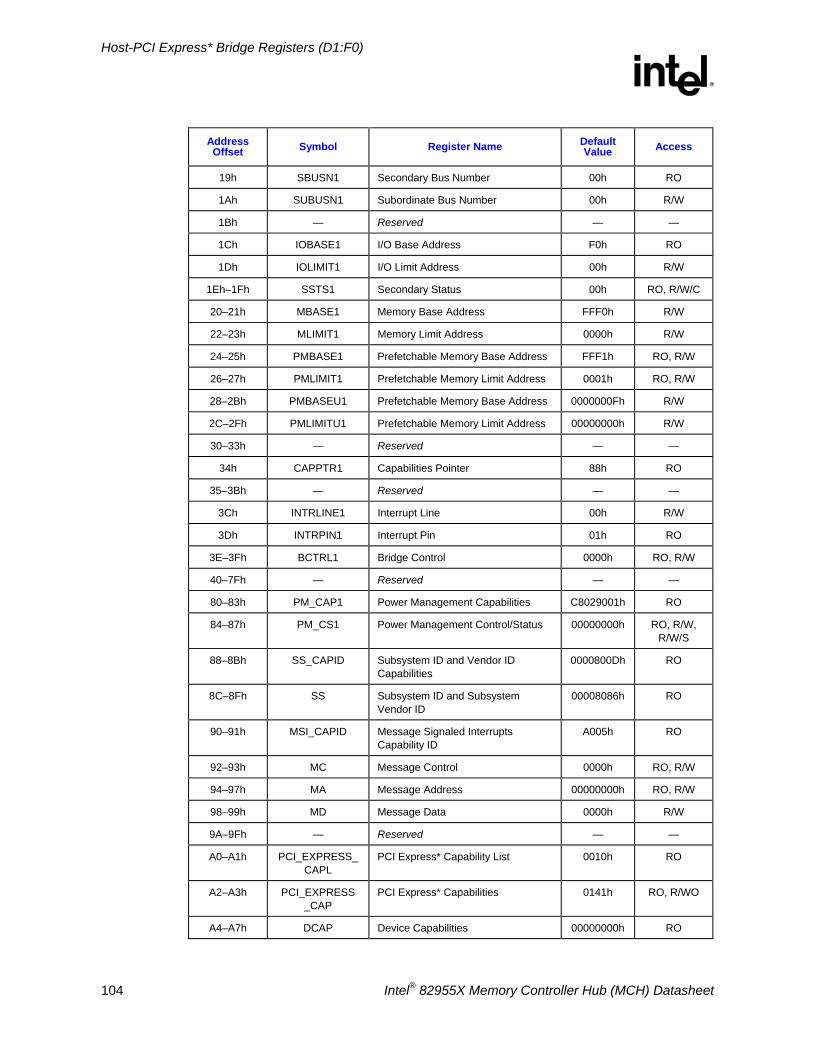
Host-PCI Express* Bridge Registers (D1:F0)
R
104 Intel® 82955X Memory Controller Hub (MCH) Datasheet
Address Offset Symbol Register Name Default
Value Access
19h SBUSN1 Secondary Bus Number 00h RO
1Ah SUBUSN1 Subordinate Bus Number 00h R/W
1Bh — Reserved — —
1Ch IOBASE1 I/O Base Address F0h RO
1Dh IOLIMIT1 I/O Limit Address 00h R/W
1Eh–1Fh SSTS1 Secondary Status 00h RO, R/W/C
20–21h MBASE1 Memory Base Address FFF0h R/W
22–23h MLIMIT1 Memory Limit Address 0000h R/W
24–25h PMBASE1 Prefetchable Memory Base Address FFF1h RO, R/W
26–27h PMLIMIT1 Prefetchable Memory Limit Address 0001h RO, R/W
28–2Bh PMBASEU1 Prefetchable Memory Base Address 0000000Fh R/W
2C–2Fh PMLIMITU1 Prefetchable Memory Limit Address 00000000h R/W
30–33h — Reserved — —
34h CAPPTR1 Capabilities Pointer 88h RO
35–3Bh — Reserved — —
3Ch INTRLINE1 Interrupt Line 00h R/W
3Dh INTRPIN1 Interrupt Pin 01h RO
3E–3Fh BCTRL1 Bridge Control 0000h RO, R/W
40–7Fh — Reserved — —
80–83h PM_CAP1 Power Management Capabilities C8029001h RO
84–87h PM_CS1 Power Management Control/Status 00000000h RO, R/W, R/W/S
88–8Bh SS_CAPID Subsystem ID and Vendor ID Capabilities
0000800Dh RO
8C–8Fh SS Subsystem ID and Subsystem Vendor ID
00008086h RO
90–91h MSI_CAPID Message Signaled Interrupts Capability ID
A005h RO
92–93h MC Message Control 0000h RO, R/W
94–97h MA Message Address 00000000h RO, R/W
98–99h MD Message Data 0000h R/W
9A–9Fh — Reserved — —
A0–A1h PCI_EXPRESS_CAPL
PCI Express* Capability List 0010h RO
A2–A3h PCI_EXPRESS _CAP
PCI Express* Capabilities 0141h RO, R/WO
A4–A7h DCAP Device Capabilities 00000000h RO
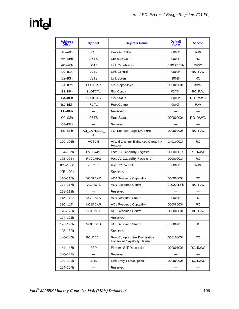
Host-PCI Express* Bridge Registers (D1:F0)
R
Intel® 82955X Memory Controller Hub (MCH) Datasheet 105
Address Offset Symbol Register Name Default
Value Access
A8–A9h DCTL Device Control 0000h R/W
AA–ABh DSTS Device Status 0000h RO
AC–AFh LCAP Link Capabilities 02012D01h R/WO
B0–B1h LCTL Link Control 0000h RO, R/W
B2–B3h LSTS Link Status 1001h RO
B4–B7h SLOTCAP Slot Capabilities 00000000h R/WO
B8–B9h SLOTCTL Slot Control 01C0h RO, R/W
BA–BBh SLOTSTS Slot Status 0000h RO, R/W/C
BC–BDh RCTL Root Control 0000h R/W
BE–BFh — Reserved — —
C0–C3h RSTS Root Status 00000000h RO, R/W/C
C4–FFh — Reserved — —
EC–EFh PCI_EXPRESS_LC
PCI Express* Legacy Control 00000000h RO, R/W
100–103h VCECH Virtual Channel Enhanced Capability Header
14010002h RO
104–107h PVCCAP1 Port VC Capability Register 1 00000001h RO, R/WO
108–10Bh PVCCAP2 Port VC Capability Register 2 00000001h RO
10C–10Dh PVCCTL Port VC Control 0000h R/W
10E–10Fh — Reserved — —
110–113h VC0RCAP VC0 Resource Capability 00000000h RO
114–117h VC0RCTL VC0 Resource Control 800000FFh RO, R/W
118–119h — Reserved — —
11A–11Bh VC0RSTS VC0 Resource Status 0002h RO
11C–11Fh VC1RCAP VC1 Resource Capability 00008000h RO
120–123h VC1RCTL VC1 Resource Control 01000000h RO, R/W
124–125h — Reserved — —
126–127h VC1RSTS VC1 Resource Status 0002h RO
128–13Fh — Reserved — —
140–143h RCLDECH Root Complex Link Declaration Enhanced Capability Header
00010005h RO
144–147h ESD Element Self Description 02000100h RO, R/WO
148–14Fh — Reserved — —
150–153h LE1D Link Entry 1 Description 00000000h RO, R/WO
154–157h — Reserved — —
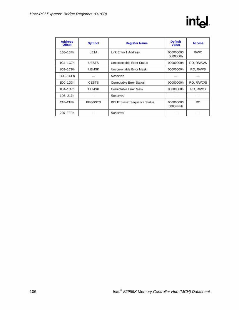
Host-PCI Express* Bridge Registers (D1:F0)
R
106 Intel® 82955X Memory Controller Hub (MCH) Datasheet
Address Offset Symbol Register Name Default
Value Access
158–15Fh LE1A Link Entry 1 Address 0000000000000000h
R/WO
1C4–1C7h UESTS Uncorrectable Error Status 00000000h RO, R/WC/S
1C8–1CBh UEMSK Uncorrectable Error Mask 00000000h RO, R/W/S
1CC–1CFh — Reserved — —
1D0–1D3h CESTS Correctable Error Status 00000000h RO, R/WC/S
1D4–1D7h CEMSK Correctable Error Mask 00000000h RO, R/W/S
1D8–217h — Reserved — —
218–21Fh PEGSSTS PCI Express* Sequence Status 0000000000000FFFh
RO
220–FFFh — Reserved — —
Host-PCI Express* Bridge Registers (D1:F0)
R
Intel® 82955X Memory Controller Hub (MCH) Datasheet 107
5.1 Configuration Register Details (D1:F0)
5.1.1 VID1—Vendor Identification (D1:F0) PCI Device: 1 Address Offset: 00–01h Default Value: 8086h Access: RO Size: 16 bits
This register combined with the Device Identification register uniquely identifies any PCI device.
Bit Access & Default
Description
15:0 RO 8086h
Vendor Identification (VID1)
PCI standard identification for Intel.
5.1.2 DID1—Device Identification (D1:F0) PCI Device: 1 Address Offset: 02–03h Default Value: 2775h Access: RO Size: 16 bits
This register combined with the Vendor Identification register uniquely identifies any PCI device.
Bit Access & Default
Description
15:0 RO 2775h
Device Identification Number (DID1): Identifier assigned to the MCH device 1 (virtual PCI-to-PCI bridge, PCI Express* Graphics port).
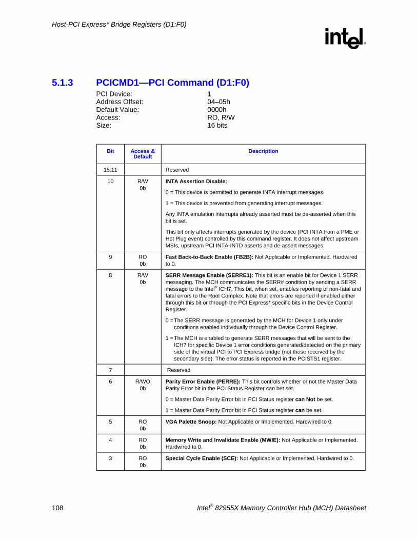
Host-PCI Express* Bridge Registers (D1:F0)
R
108 Intel® 82955X Memory Controller Hub (MCH) Datasheet
5.1.3 PCICMD1—PCI Command (D1:F0) PCI Device: 1 Address Offset: 04–05h Default Value: 0000h Access: RO, R/W Size: 16 bits
Bit Access &
Default Description
15:11 Reserved
10 R/W 0b
INTA Assertion Disable:
0 = This device is permitted to generate INTA interrupt messages.
1 = This device is prevented from generating interrupt messages.
Any INTA emulation interrupts already asserted must be de-asserted when this bit is set.
This bit only affects interrupts generated by the device (PCI INTA from a PME or Hot Plug event) controlled by this command register. It does not affect upstream MSIs, upstream PCI INTA-INTD asserts and de-assert messages.
9 RO 0b
Fast Back-to-Back Enable (FB2B): Not Applicable or Implemented. Hardwired to 0.
8 R/W 0b
SERR Message Enable (SERRE1): This bit is an enable bit for Device 1 SERR messaging. The MCH communicates the SERR# condition by sending a SERR message to the Intel® ICH7. This bit, when set, enables reporting of non-fatal and fatal errors to the Root Complex. Note that errors are reported if enabled either through this bit or through the PCI Express* specific bits in the Device Control Register.
0 = The SERR message is generated by the MCH for Device 1 only under conditions enabled individually through the Device Control Register.
1 = The MCH is enabled to generate SERR messages that will be sent to the ICH7 for specific Device 1 error conditions generated/detected on the primary side of the virtual PCI to PCI Express bridge (not those received by the secondary side). The error status is reported in the PCISTS1 register.
7 Reserved
6 R/WO 0b
Parity Error Enable (PERRE): This bit controls whether or not the Master Data Parity Error bit in the PCI Status Register can bet set.
0 = Master Data Parity Error bit in PCI Status register can Not be set.
1 = Master Data Parity Error bit in PCI Status register can be set.
5 RO 0b
VGA Palette Snoop: Not Applicable or Implemented. Hardwired to 0.
4 RO 0b
Memory Write and Invalidate Enable (MWIE): Not Applicable or Implemented. Hardwired to 0.
3 RO 0b
Special Cycle Enable (SCE): Not Applicable or Implemented. Hardwired to 0.
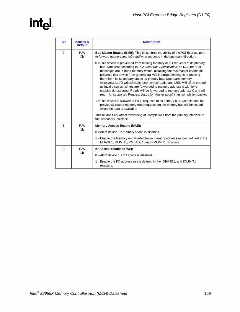
Host-PCI Express* Bridge Registers (D1:F0)
R
Intel® 82955X Memory Controller Hub (MCH) Datasheet 109
Bit Access & Default
Description
2 R/W 0b
Bus Master Enable (BME): This bit controls the ability of the PCI Express port to forward memory and I/O read/write requests in the upstream direction.
0 = This device is prevented from making memory or I/O requests to its primary bus. Note that according to PCI Local Bus Specification, as MSI interrupt messages are in-band memory writes, disabling the bus master enable bit prevents this device from generating MSI interrupt messages or passing them from its secondary bus to its primary bus. Upstream memory writes/reads, I/O writes/reads, peer writes/reads, and MSIs will all be treated as invalid cycles. Writes are forwarded to memory address 0 with byte enables de-asserted. Reads will be forwarded to memory address 0 and will return Unsupported Request status (or Master abort) in its completion packet.
1 = This device is allowed to issue requests to its primary bus. Completions for previously issued memory read requests on the primary bus will be issued when the data is available.
This bit does not affect forwarding of Completions from the primary interface to the secondary interface.
1 R/W 0b
Memory Access Enable (MAE):
0 = All of device 1’s memory space is disabled.
1 = Enable the Memory and Pre-fetchable memory address ranges defined in the MBASE1, MLIMIT1, PMBASE1, and PMLIMIT1 registers.
0 R/W 0b
IO Access Enable (IOAE):
0 = All of device 1’s I/O space is disabled.
1 = Enable the I/O address range defined in the IOBASE1, and IOLIMIT1 registers.
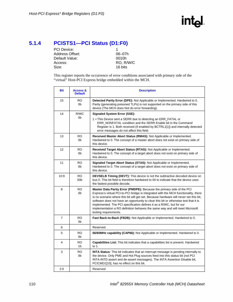
Host-PCI Express* Bridge Registers (D1:F0)
R
110 Intel® 82955X Memory Controller Hub (MCH) Datasheet
5.1.4 PCISTS1—PCI Status (D1:F0) PCI Device: 1 Address Offset: 06–07h Default Value: 0010h Access: RO, R/W/C Size: 16 bits
This register reports the occurrence of error conditions associated with primary side of the “virtual” Host-PCI Express bridge embedded within the MCH.
Bit Access & Default
Description
15 RO 0b
Detected Parity Error (DPE): Not Applicable or Implemented. Hardwired to 0. Parity (generating poisoned TLPs) is not supported on the primary side of this device (The MCH does Not do error forwarding).
14 R/WC 0b
Signaled System Error (SSE):
1 = This Device sent a SERR due to detecting an ERR_FATAL or ERR_NONFATAL condition and the SERR Enable bit in the Command Register is 1. Both received (if enabled by BCTRL1[1]) and internally detected error messages do not affect this field.
13 RO 0b
Received Master Abort Status (RMAS): Not Applicable or Implemented. Hardwired to 0. The concept of a master abort does not exist on primary side of this device.
12 RO 0b
Received Target Abort Status (RTAS): Not Applicable or Implemented. Hardwired to 0. The concept of a target abort does not exist on primary side of this device.
11 RO 0b
Signaled Target Abort Status (STAS): Not Applicable or Implemented. Hardwired to 0. The concept of a target abort does not exist on primary side of this device.
10:9 RO 00b
DEVSELB Timing (DEVT): This device is not the subtractive decoded device on bus 0. This bit field is therefore hardwired to 00 to indicate that the device uses the fastest possible decode.
8 RO 0b
Master Data Parity Error (PMDPE): Because the primary side of the PCI Express’s virtual PCI-to-PCI bridge is integrated with the MCH functionality, there is no scenario where this bit will get set. Because hardware will never set this bit, software does not have an opportunity to clear this bit or otherwise test that it is implemented. The PCI specification defines it as a R/WC, but for our implementation a RO definition behaves the same way and will meet Microsoft testing requirements.
7 RO 0b
Fast Back-to-Back (FB2B): Not Applicable or Implemented. Hardwired to 0.
6 Reserved
5 RO 0b
66/60MHz capability (CAP66): Not Applicable or Implemented. Hardwired to 0.
4 RO 1b
Capabilities List: This bit indicates that a capabilities list is present. Hardwired to 1.
3 RO 0b
INTA Status: This bit indicates that an interrupt message is pending internally to the device. Only PME and Hot Plug sources feed into this status bit (not PCI INTA-INTD assert and de-assert messages). The INTA Assertion Disable bit, PCICMD1[10], has no effect on this bit.
2:0 Reserved
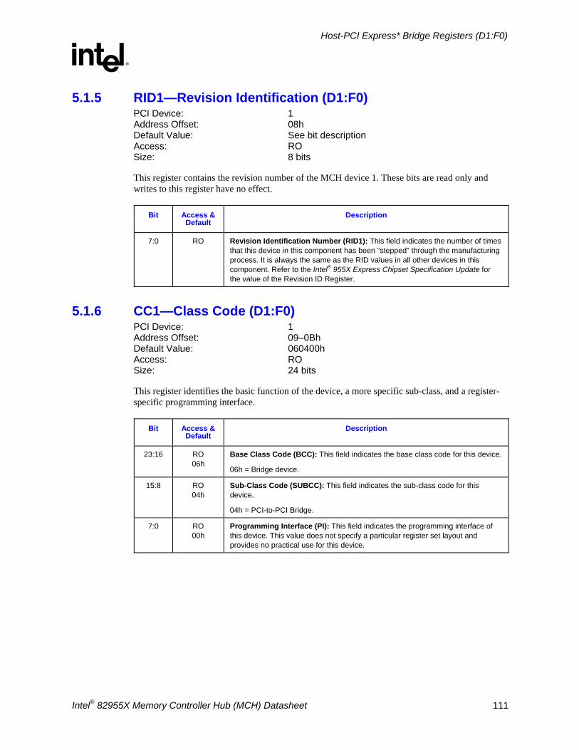
Host-PCI Express* Bridge Registers (D1:F0)
R
Intel® 82955X Memory Controller Hub (MCH) Datasheet 111
5.1.5 RID1—Revision Identification (D1:F0) PCI Device: 1 Address Offset: 08h Default Value: See bit description Access: RO Size: 8 bits
This register contains the revision number of the MCH device 1. These bits are read only and writes to this register have no effect.
Bit Access & Default
Description
7:0 RO Revision Identification Number (RID1): This field indicates the number of times that this device in this component has been “stepped” through the manufacturing process. It is always the same as the RID values in all other devices in this component. Refer to the Intel® 955X Express Chipset Specification Update for the value of the Revision ID Register.
5.1.6 CC1—Class Code (D1:F0) PCI Device: 1 Address Offset: 09–0Bh Default Value: 060400h Access: RO Size: 24 bits
This register identifies the basic function of the device, a more specific sub-class, and a register-specific programming interface.
Bit Access & Default
Description
23:16 RO 06h
Base Class Code (BCC): This field indicates the base class code for this device.
06h = Bridge device.
15:8 RO 04h
Sub-Class Code (SUBCC): This field indicates the sub-class code for this device.
04h = PCI-to-PCI Bridge.
7:0 RO 00h
Programming Interface (PI): This field indicates the programming interface of this device. This value does not specify a particular register set layout and provides no practical use for this device.
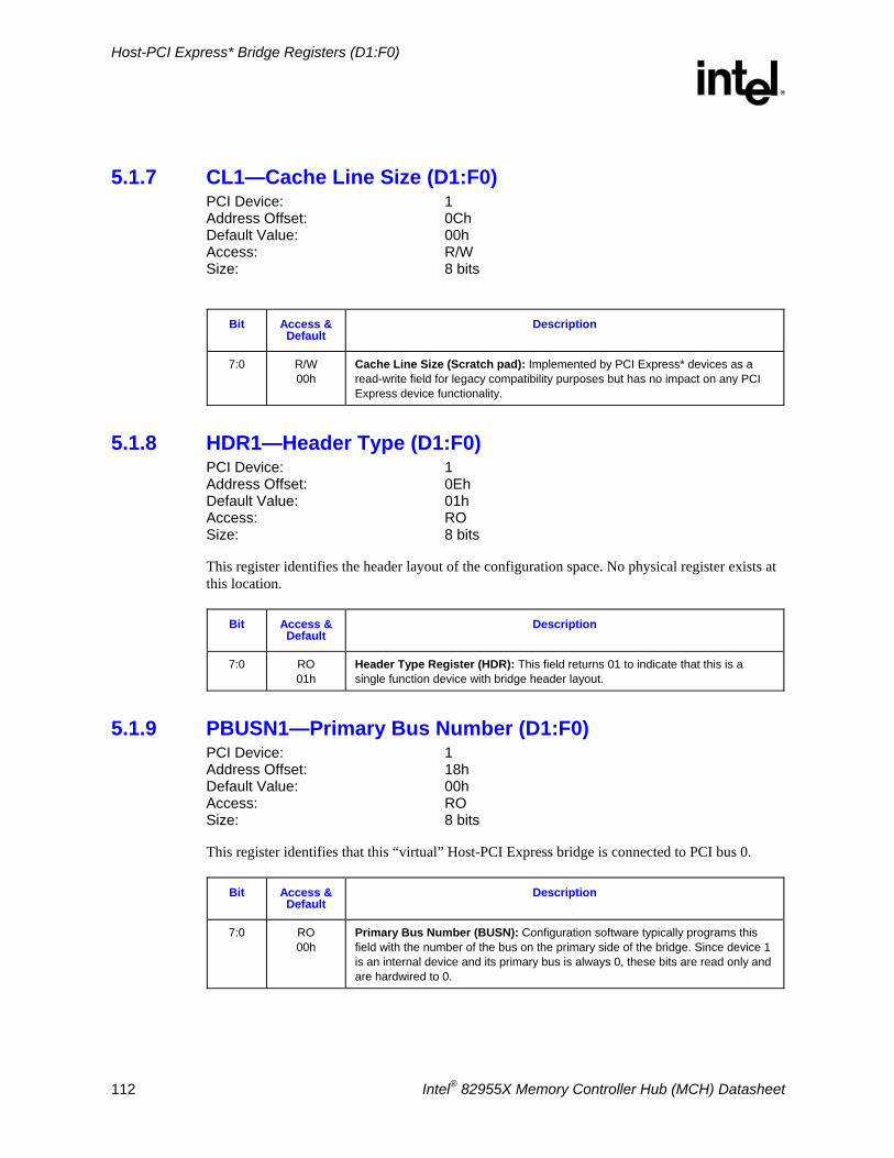
Host-PCI Express* Bridge Registers (D1:F0)
R
112 Intel® 82955X Memory Controller Hub (MCH) Datasheet
5.1.7 CL1—Cache Line Size (D1:F0) PCI Device: 1 Address Offset: 0Ch Default Value: 00h Access: R/W Size: 8 bits
Bit Access &
Default Description
7:0 R/W 00h
Cache Line Size (Scratch pad): Implemented by PCI Express* devices as a read-write field for legacy compatibility purposes but has no impact on any PCI Express device functionality.
5.1.8 HDR1—Header Type (D1:F0) PCI Device: 1 Address Offset: 0Eh Default Value: 01h Access: RO Size: 8 bits
This register identifies the header layout of the configuration space. No physical register exists at this location.
Bit Access & Default
Description
7:0 RO 01h
Header Type Register (HDR): This field returns 01 to indicate that this is a single function device with bridge header layout.
5.1.9 PBUSN1—Primary Bus Number (D1:F0) PCI Device: 1 Address Offset: 18h Default Value: 00h Access: RO Size: 8 bits
This register identifies that this “virtual” Host-PCI Express bridge is connected to PCI bus 0.
Bit Access & Default
Description
7:0 RO 00h
Primary Bus Number (BUSN): Configuration software typically programs this field with the number of the bus on the primary side of the bridge. Since device 1 is an internal device and its primary bus is always 0, these bits are read only and are hardwired to 0.
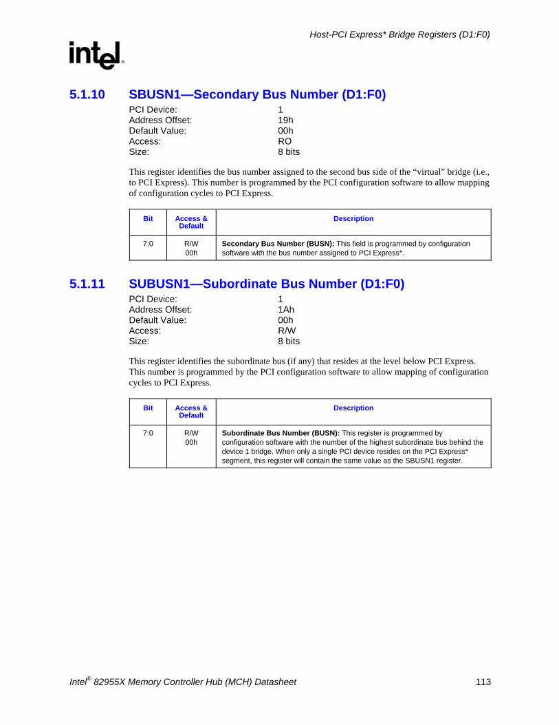
Host-PCI Express* Bridge Registers (D1:F0)
R
Intel® 82955X Memory Controller Hub (MCH) Datasheet 113
5.1.10 SBUSN1—Secondary Bus Number (D1:F0) PCI Device: 1 Address Offset: 19h Default Value: 00h Access: RO Size: 8 bits
This register identifies the bus number assigned to the second bus side of the “virtual” bridge (i.e., to PCI Express). This number is programmed by the PCI configuration software to allow mapping of configuration cycles to PCI Express.
Bit Access & Default
Description
7:0 R/W 00h
Secondary Bus Number (BUSN): This field is programmed by configuration software with the bus number assigned to PCI Express*.
5.1.11 SUBUSN1—Subordinate Bus Number (D1:F0) PCI Device: 1 Address Offset: 1Ah Default Value: 00h Access: R/W Size: 8 bits
This register identifies the subordinate bus (if any) that resides at the level below PCI Express. This number is programmed by the PCI configuration software to allow mapping of configuration cycles to PCI Express.
Bit Access & Default
Description
7:0 R/W 00h
Subordinate Bus Number (BUSN): This register is programmed by configuration software with the number of the highest subordinate bus behind the device 1 bridge. When only a single PCI device resides on the PCI Express* segment, this register will contain the same value as the SBUSN1 register.
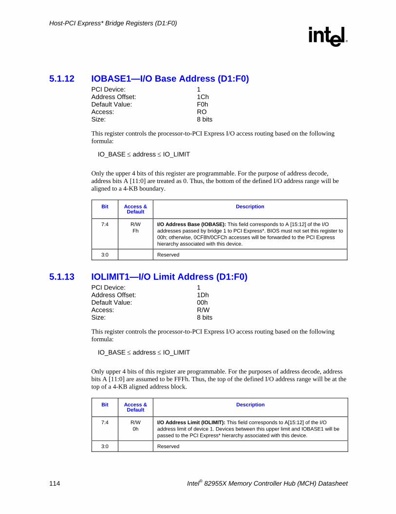
Host-PCI Express* Bridge Registers (D1:F0)
R
114 Intel® 82955X Memory Controller Hub (MCH) Datasheet
5.1.12 IOBASE1—I/O Base Address (D1:F0) PCI Device: 1 Address Offset: 1Ch Default Value: F0h Access: RO Size: 8 bits
This register controls the processor-to-PCI Express I/O access routing based on the following formula:
IO_BASE ≤ address ≤ IO_LIMIT
Only the upper 4 bits of this register are programmable. For the purpose of address decode, address bits A [11:0] are treated as 0. Thus, the bottom of the defined I/O address range will be aligned to a 4-KB boundary.
Bit Access & Default
Description
7:4 R/W Fh
I/O Address Base (IOBASE): This field corresponds to A [15:12] of the I/O addresses passed by bridge 1 to PCI Express*. BIOS must not set this register to 00h; otherwise, 0CF8h/0CFCh accesses will be forwarded to the PCI Express hierarchy associated with this device.
3:0 Reserved
5.1.13 IOLIMIT1—I/O Limit Address (D1:F0) PCI Device: 1 Address Offset: 1Dh Default Value: 00h Access: R/W Size: 8 bits
This register controls the processor-to-PCI Express I/O access routing based on the following formula:
IO_BASE ≤ address ≤ IO_LIMIT
Only upper 4 bits of this register are programmable. For the purposes of address decode, address bits A [11:0] are assumed to be FFFh. Thus, the top of the defined I/O address range will be at the top of a 4-KB aligned address block.
Bit Access & Default
Description
7:4 R/W 0h
I/O Address Limit (IOLIMIT): This field corresponds to A[15:12] of the I/O address limit of device 1. Devices between this upper limit and IOBASE1 will be passed to the PCI Express* hierarchy associated with this device.
3:0 Reserved
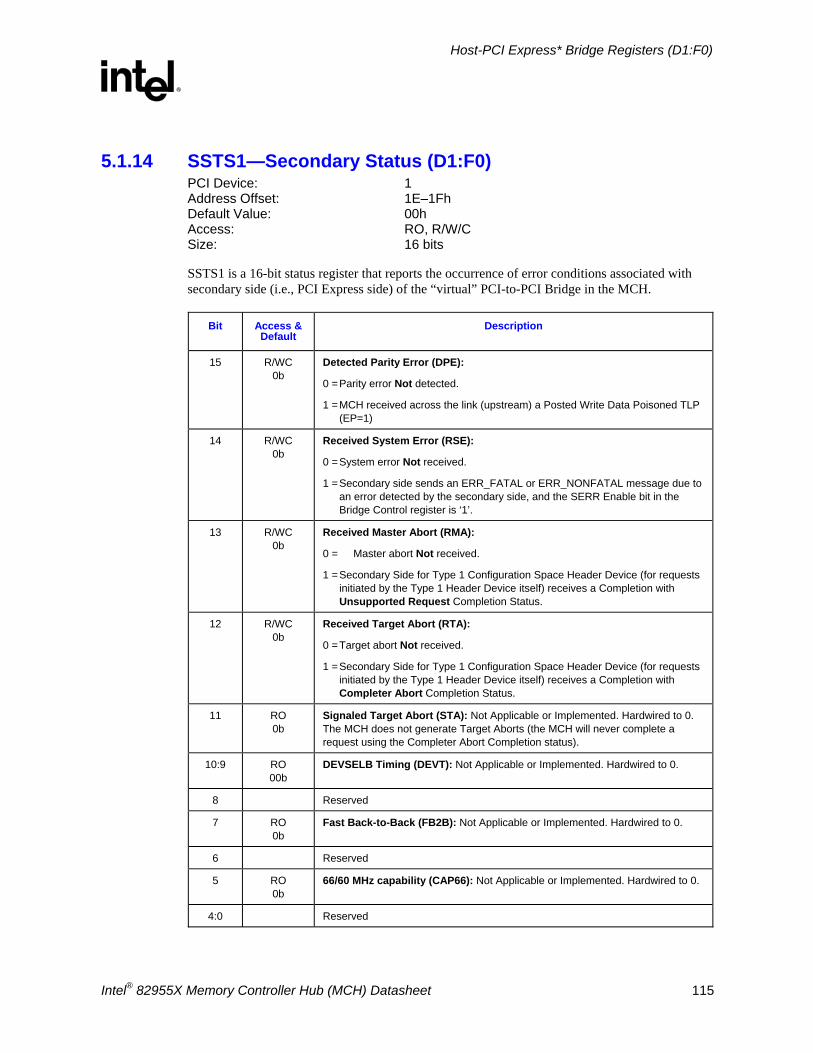
Host-PCI Express* Bridge Registers (D1:F0)
R
Intel® 82955X Memory Controller Hub (MCH) Datasheet 115
5.1.14 SSTS1—Secondary Status (D1:F0) PCI Device: 1 Address Offset: 1E–1Fh Default Value: 00h Access: RO, R/W/C Size: 16 bits
SSTS1 is a 16-bit status register that reports the occurrence of error conditions associated with secondary side (i.e., PCI Express side) of the “virtual” PCI-to-PCI Bridge in the MCH.
Bit Access & Default
Description
15 R/WC 0b
Detected Parity Error (DPE):
0 = Parity error Not detected.
1 = MCH received across the link (upstream) a Posted Write Data Poisoned TLP (EP=1)
14 R/WC 0b
Received System Error (RSE):
0 = System error Not received.
1 = Secondary side sends an ERR_FATAL or ERR_NONFATAL message due to an error detected by the secondary side, and the SERR Enable bit in the Bridge Control register is ‘1’.
13 R/WC 0b
Received Master Abort (RMA):
0 = Master abort Not received.
1 = Secondary Side for Type 1 Configuration Space Header Device (for requests initiated by the Type 1 Header Device itself) receives a Completion with Unsupported Request Completion Status.
12 R/WC 0b
Received Target Abort (RTA):
0 = Target abort Not received.
1 = Secondary Side for Type 1 Configuration Space Header Device (for requests initiated by the Type 1 Header Device itself) receives a Completion with Completer Abort Completion Status.
11 RO 0b
Signaled Target Abort (STA): Not Applicable or Implemented. Hardwired to 0. The MCH does not generate Target Aborts (the MCH will never complete a request using the Completer Abort Completion status).
10:9 RO 00b
DEVSELB Timing (DEVT): Not Applicable or Implemented. Hardwired to 0.
8 Reserved
7 RO 0b
Fast Back-to-Back (FB2B): Not Applicable or Implemented. Hardwired to 0.
6 Reserved
5 RO 0b
66/60 MHz capability (CAP66): Not Applicable or Implemented. Hardwired to 0.
4:0 Reserved
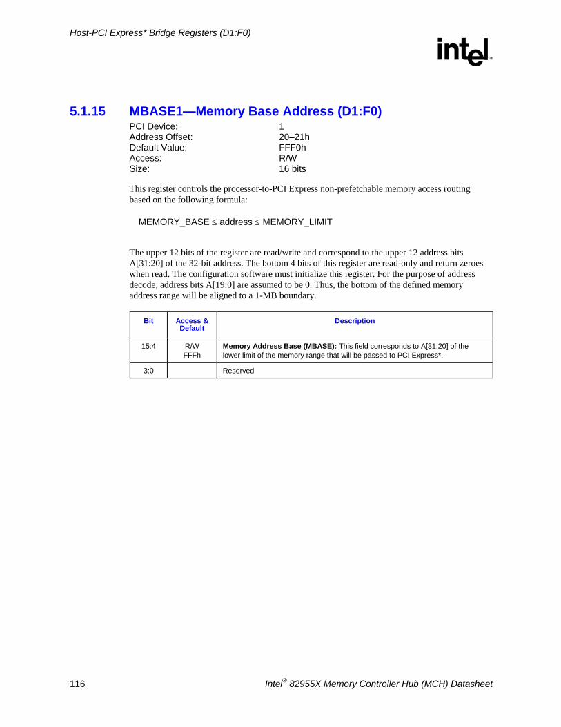
Host-PCI Express* Bridge Registers (D1:F0)
R
116 Intel® 82955X Memory Controller Hub (MCH) Datasheet
5.1.15 MBASE1—Memory Base Address (D1:F0) PCI Device: 1 Address Offset: 20–21h Default Value: FFF0h Access: R/W Size: 16 bits
This register controls the processor-to-PCI Express non-prefetchable memory access routing based on the following formula:
MEMORY_BASE ≤ address ≤ MEMORY_LIMIT
The upper 12 bits of the register are read/write and correspond to the upper 12 address bits A[31:20] of the 32-bit address. The bottom 4 bits of this register are read-only and return zeroes when read. The configuration software must initialize this register. For the purpose of address decode, address bits A[19:0] are assumed to be 0. Thus, the bottom of the defined memory address range will be aligned to a 1-MB boundary.
Bit Access & Default
Description
15:4 R/W FFFh
Memory Address Base (MBASE): This field corresponds to A[31:20] of the lower limit of the memory range that will be passed to PCI Express*.
3:0 Reserved
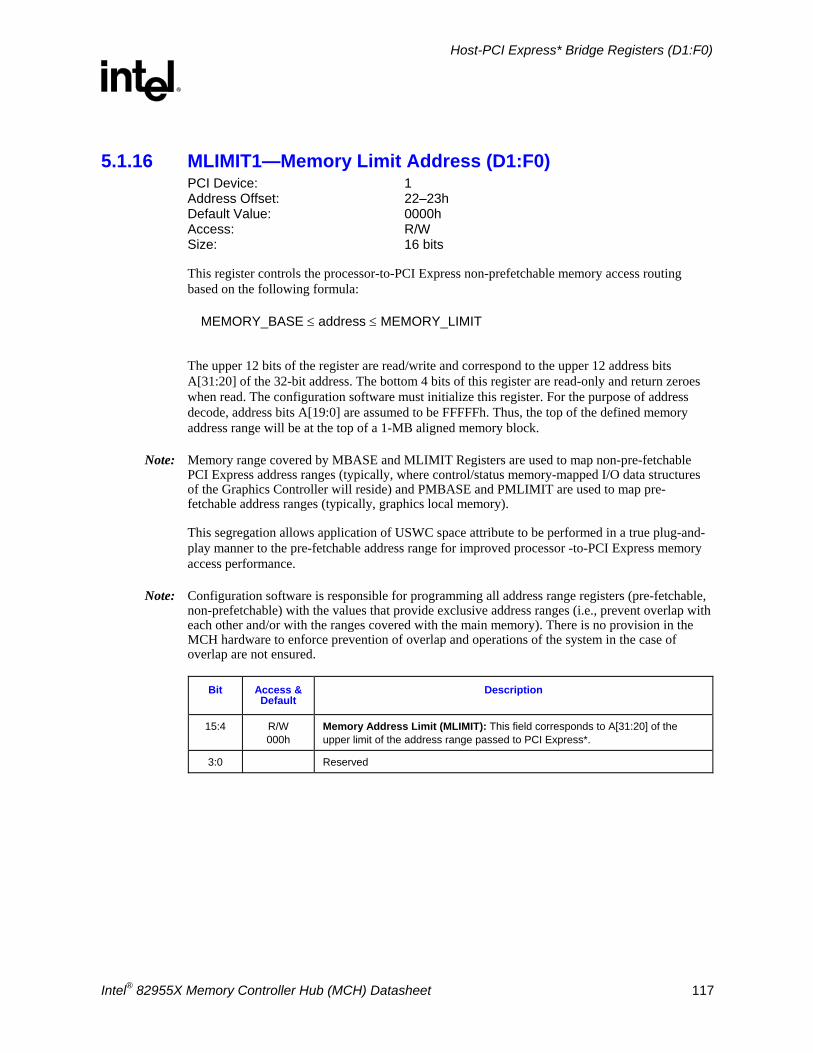
Host-PCI Express* Bridge Registers (D1:F0)
R
Intel® 82955X Memory Controller Hub (MCH) Datasheet 117
5.1.16 MLIMIT1—Memory Limit Address (D1:F0) PCI Device: 1 Address Offset: 22–23h Default Value: 0000h Access: R/W Size: 16 bits
This register controls the processor-to-PCI Express non-prefetchable memory access routing based on the following formula:
MEMORY_BASE ≤ address ≤ MEMORY_LIMIT
The upper 12 bits of the register are read/write and correspond to the upper 12 address bits A[31:20] of the 32-bit address. The bottom 4 bits of this register are read-only and return zeroes when read. The configuration software must initialize this register. For the purpose of address decode, address bits A[19:0] are assumed to be FFFFFh. Thus, the top of the defined memory address range will be at the top of a 1-MB aligned memory block.
Note: Memory range covered by MBASE and MLIMIT Registers are used to map non-pre-fetchable PCI Express address ranges (typically, where control/status memory-mapped I/O data structures of the Graphics Controller will reside) and PMBASE and PMLIMIT are used to map pre-fetchable address ranges (typically, graphics local memory).
This segregation allows application of USWC space attribute to be performed in a true plug-and-play manner to the pre-fetchable address range for improved processor -to-PCI Express memory access performance.
Note: Configuration software is responsible for programming all address range registers (pre-fetchable, non-prefetchable) with the values that provide exclusive address ranges (i.e., prevent overlap with each other and/or with the ranges covered with the main memory). There is no provision in the MCH hardware to enforce prevention of overlap and operations of the system in the case of overlap are not ensured.
Bit Access & Default
Description
15:4 R/W 000h
Memory Address Limit (MLIMIT): This field corresponds to A[31:20] of the upper limit of the address range passed to PCI Express*.
3:0 Reserved
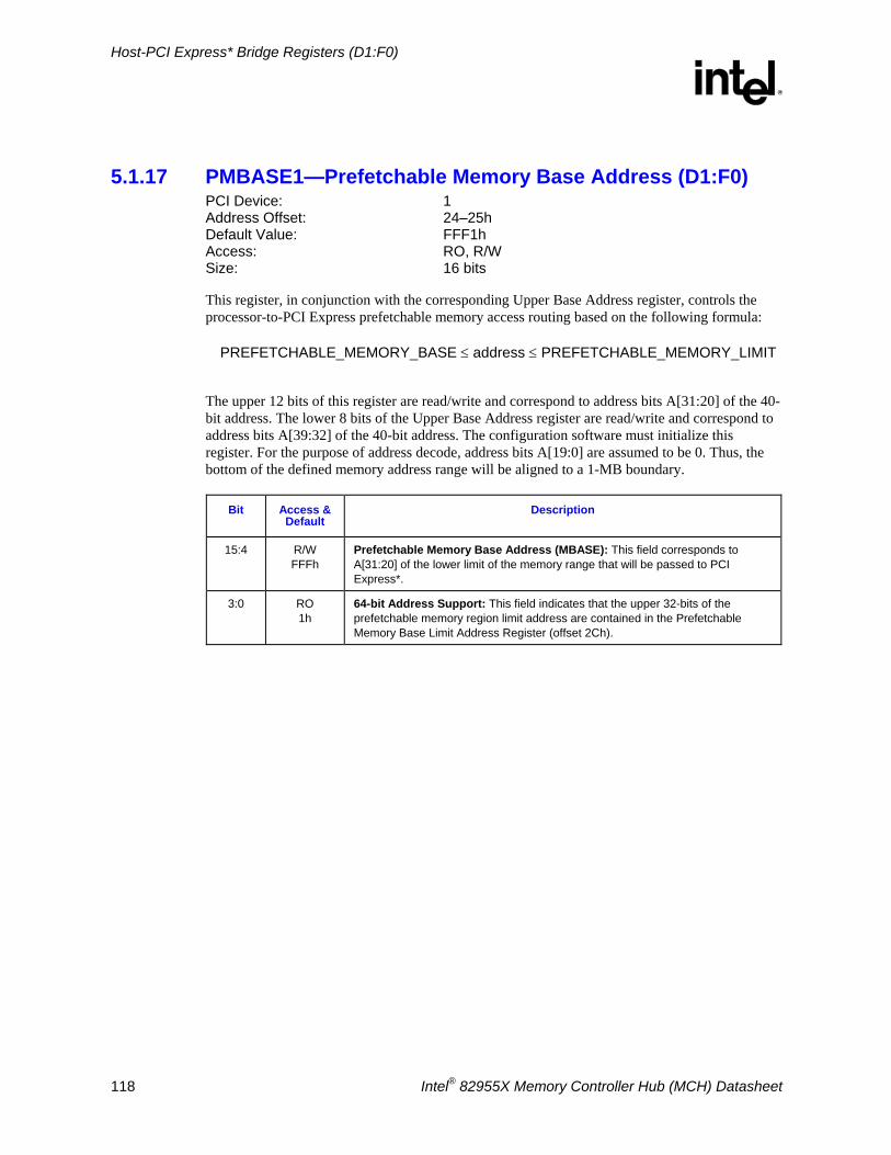
Host-PCI Express* Bridge Registers (D1:F0)
R
118 Intel® 82955X Memory Controller Hub (MCH) Datasheet
5.1.17 PMBASE1—Prefetchable Memory Base Address (D1:F0) PCI Device: 1 Address Offset: 24–25h Default Value: FFF1h Access: RO, R/W Size: 16 bits
This register, in conjunction with the corresponding Upper Base Address register, controls the processor-to-PCI Express prefetchable memory access routing based on the following formula:
PREFETCHABLE_MEMORY_BASE ≤ address ≤ PREFETCHABLE_MEMORY_LIMIT
The upper 12 bits of this register are read/write and correspond to address bits A[31:20] of the 40-bit address. The lower 8 bits of the Upper Base Address register are read/write and correspond to address bits A[39:32] of the 40-bit address. The configuration software must initialize this register. For the purpose of address decode, address bits A[19:0] are assumed to be 0. Thus, the bottom of the defined memory address range will be aligned to a 1-MB boundary.
Bit Access & Default
Description
15:4 R/W FFFh
Prefetchable Memory Base Address (MBASE): This field corresponds to A[31:20] of the lower limit of the memory range that will be passed to PCI Express*.
3:0 RO 1h
64-bit Address Support: This field indicates that the upper 32-bits of the prefetchable memory region limit address are contained in the Prefetchable Memory Base Limit Address Register (offset 2Ch).
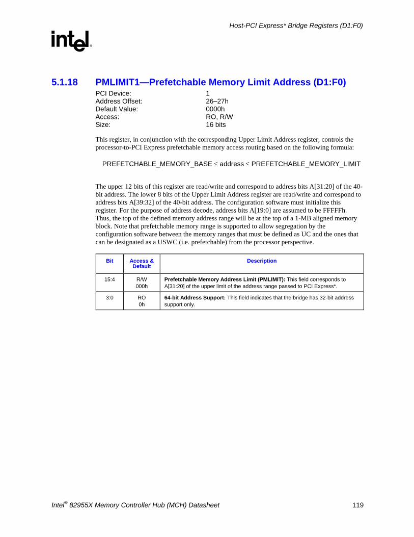
Host-PCI Express* Bridge Registers (D1:F0)
R
Intel® 82955X Memory Controller Hub (MCH) Datasheet 119
5.1.18 PMLIMIT1—Prefetchable Memory Limit Address (D1:F0) PCI Device: 1 Address Offset: 26–27h Default Value: 0000h Access: RO, R/W Size: 16 bits
This register, in conjunction with the corresponding Upper Limit Address register, controls the processor-to-PCI Express prefetchable memory access routing based on the following formula:
PREFETCHABLE_MEMORY_BASE ≤ address ≤ PREFETCHABLE_MEMORY_LIMIT
The upper 12 bits of this register are read/write and correspond to address bits A[31:20] of the 40-bit address. The lower 8 bits of the Upper Limit Address register are read/write and correspond to address bits A[39:32] of the 40-bit address. The configuration software must initialize this register. For the purpose of address decode, address bits A[19:0] are assumed to be FFFFFh. Thus, the top of the defined memory address range will be at the top of a 1-MB aligned memory block. Note that prefetchable memory range is supported to allow segregation by the configuration software between the memory ranges that must be defined as UC and the ones that can be designated as a USWC (i.e. prefetchable) from the processor perspective.
Bit Access & Default
Description
15:4 R/W 000h
Prefetchable Memory Address Limit (PMLIMIT): This field corresponds to A[31:20] of the upper limit of the address range passed to PCI Express*.
3:0 RO 0h
64-bit Address Support: This field indicates that the bridge has 32-bit address support only.
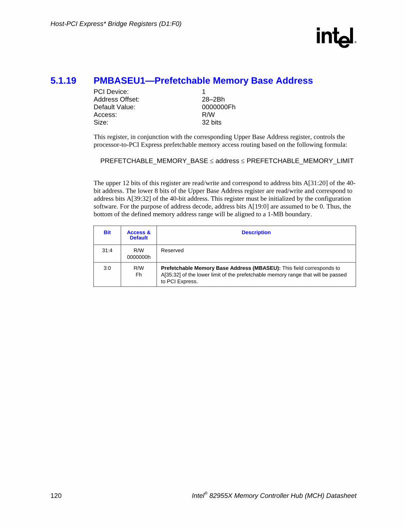
Host-PCI Express* Bridge Registers (D1:F0)
R
120 Intel® 82955X Memory Controller Hub (MCH) Datasheet
5.1.19 PMBASEU1—Prefetchable Memory Base Address PCI Device: 1 Address Offset: 28–2Bh Default Value: 0000000Fh Access: R/W Size: 32 bits
This register, in conjunction with the corresponding Upper Base Address register, controls the processor-to-PCI Express prefetchable memory access routing based on the following formula:
PREFETCHABLE_MEMORY_BASE ≤ address ≤ PREFETCHABLE_MEMORY_LIMIT
The upper 12 bits of this register are read/write and correspond to address bits A[31:20] of the 40-bit address. The lower 8 bits of the Upper Base Address register are read/write and correspond to address bits A[39:32] of the 40-bit address. This register must be initialized by the configuration software. For the purpose of address decode, address bits A[19:0] are assumed to be 0. Thus, the bottom of the defined memory address range will be aligned to a 1-MB boundary.
Bit Access & Default
Description
31:4 R/W 0000000h
Reserved
3:0 R/W Fh
Prefetchable Memory Base Address (MBASEU): This field corresponds to A[35:32] of the lower limit of the prefetchable memory range that will be passed to PCI Express.
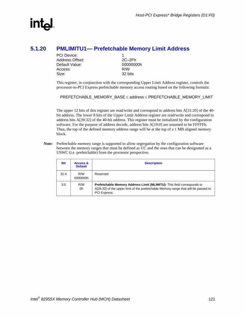
Host-PCI Express* Bridge Registers (D1:F0)
R
Intel® 82955X Memory Controller Hub (MCH) Datasheet 121
5.1.20 PMLIMITU1— Prefetchable Memory Limit Address PCI Device: 1 Address Offset: 2C–2Fh Default Value: 00000000h Access: R/W Size: 32 bits
This register, in conjunction with the corresponding Upper Limit Address register, controls the processor-to-PCI Express prefetchable memory access routing based on the following formula:
PREFETCHABLE_MEMORY_BASE ≤ address ≤ PREFETCHABLE_MEMORY_LIMIT
The upper 12 bits of this register are read/write and correspond to address bits A[31:20] of the 40-bit address. The lower 8 bits of the Upper Limit Address register are read/write and correspond to address bits A[39:32] of the 40-bit address. This register must be initialized by the configuration software. For the purpose of address decode, address bits A[19:0] are assumed to be FFFFFh. Thus, the top of the defined memory address range will be at the top of a 1 MB aligned memory block.
Note: Prefetchable memory range is supported to allow segregation by the configuration software between the memory ranges that must be defined as UC and the ones that can be designated as a USWC (i.e. prefetchable) from the processor perspective.
Bit Access & Default
Description
31:4 R/W 0000000h
Reserved
3:0 R/W 0h
Prefetchable Memory Address Limit (MLIMITU): This field corresponds to A[35:32] of the upper limit of the prefetchable Memory range that will be passed to PCI Express.
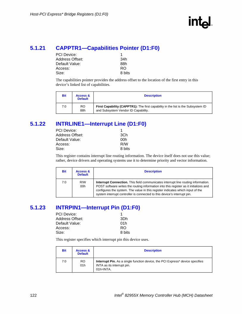
Host-PCI Express* Bridge Registers (D1:F0)
R
122 Intel® 82955X Memory Controller Hub (MCH) Datasheet
5.1.21 CAPPTR1—Capabilities Pointer (D1:F0) PCI Device: 1 Address Offset: 34h Default Value: 88h Access: RO Size: 8 bits
The capabilities pointer provides the address offset to the location of the first entry in this device’s linked list of capabilities.
Bit Access & Default
Description
7:0 RO 88h
First Capability (CAPPTR1): The first capability in the list is the Subsystem ID and Subsystem Vendor ID Capability.
5.1.22 INTRLINE1—Interrupt Line (D1:F0) PCI Device: 1 Address Offset: 3Ch Default Value: 00h Access: R/W Size: 8 bits
This register contains interrupt line routing information. The device itself does not use this value; rather, device drivers and operating systems use it to determine priority and vector information.
Bit Access & Default
Description
7:0 R/W 00h
Interrupt Connection. This field communicates interrupt line routing information. POST software writes the routing information into this register as it initializes and configures the system. The value in this register indicates which input of the system interrupt controller is connected to this device’s interrupt pin.
5.1.23 INTRPIN1—Interrupt Pin (D1:F0) PCI Device: 1 Address Offset: 3Dh Default Value: 01h Access: RO Size: 8 bits
This register specifies which interrupt pin this device uses.
Bit Access & Default
Description
7:0 RO 01h
Interrupt Pin. As a single function device, the PCI Express* device specifies INTA as its interrupt pin. 01h=INTA.
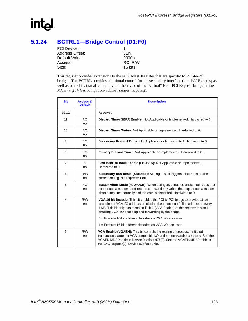
Host-PCI Express* Bridge Registers (D1:F0)
R
Intel® 82955X Memory Controller Hub (MCH) Datasheet 123
5.1.24 BCTRL1—Bridge Control (D1:F0) PCI Device: 1 Address Offset: 3Eh Default Value: 0000h Access: RO, R/W Size: 16 bits
This register provides extensions to the PCICMD1 Register that are specific to PCI-to-PCI bridges. The BCTRL provides additional control for the secondary interface (i.e., PCI Express) as well as some bits that affect the overall behavior of the “virtual” Host-PCI Express bridge in the MCH (e.g., VGA compatible address ranges mapping).
Bit Access & Default
Description
15:12 Reserved
11 RO 0b
Discard Timer SERR Enable: Not Applicable or Implemented. Hardwired to 0.
10 RO 0b
Discard Timer Status: Not Applicable or Implemented. Hardwired to 0.
9 RO 0b
Secondary Discard Timer: Not Applicable or Implemented. Hardwired to 0.
8 RO 0b
Primary Discard Timer: Not Applicable or Implemented. Hardwired to 0.
7 RO 0b
Fast Back-to-Back Enable (FB2BEN): Not Applicable or Implemented. Hardwired to 0.
6 R/W 0b
Secondary Bus Reset (SRESET): Setting this bit triggers a hot reset on the corresponding PCI Express* Port.
5 RO 0b
Master Abort Mode (MAMODE): When acting as a master, unclaimed reads that experience a master abort returns all 1s and any writes that experience a master abort completes normally and the data is discarded. Hardwired to 0.
4 R/W 0b
VGA 16-bit Decode: This bit enables the PCI-to-PCI bridge to provide 16-bit decoding of VGA I/O address precluding the decoding of alias addresses every 1 KB. This bit only has meaning if bit 3 (VGA Enable) of this register is also 1, enabling VGA I/O decoding and forwarding by the bridge.
0 = Execute 10-bit address decodes on VGA I/O accesses.
1 = Execute 16-bit address decodes on VGA I/O accesses.
3 R/W 0b
VGA Enable (VGAEN): This bit controls the routing of processor-initiated transactions targeting VGA compatible I/O and memory address ranges. See the VGAEN/MDAP table in Device 0, offset 97h[0]. See the VGAEN/MDAP table in the LAC Register[0] (Device 0, offset 97h).
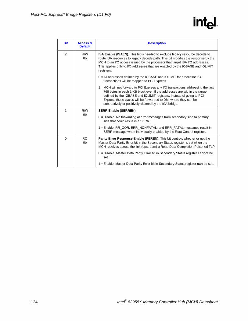
Host-PCI Express* Bridge Registers (D1:F0)
R
124 Intel® 82955X Memory Controller Hub (MCH) Datasheet
Bit Access & Default
Description
2 R/W 0b
ISA Enable (ISAEN): This bit is needed to exclude legacy resource decode to route ISA resources to legacy decode path. This bit modifies the response by the MCH to an I/O access issued by the processor that target ISA I/O addresses. This applies only to I/O addresses that are enabled by the IOBASE and IOLIMIT registers.
0 = All addresses defined by the IOBASE and IOLIMIT for processor I/O transactions will be mapped to PCI Express.
1 = MCH will not forward to PCI Express any I/O transactions addressing the last 768 bytes in each 1-KB block even if the addresses are within the range defined by the IOBASE and IOLIMIT registers. Instead of going to PCI Express these cycles will be forwarded to DMI where they can be subtractively or positively claimed by the ISA bridge.
1 R/W 0b
SERR Enable (SERREN)
0 = Disable. No forwarding of error messages from secondary side to primary side that could result in a SERR.
1 = Enable. RR_COR, ERR_NONFATAL, and ERR_FATAL messages result in SERR message when individually enabled by the Root Control register.
0 RO 0b
Parity Error Response Enable (PEREN): This bit controls whether or not the Master Data Parity Error bit in the Secondary Status register is set when the MCH receives across the link (upstream) a Read Data Completion Poisoned TLP
0 = Disable. Master Data Parity Error bit in Secondary Status register cannot be set.
1 = Enable. Master Data Parity Error bit in Secondary Status register can be set..
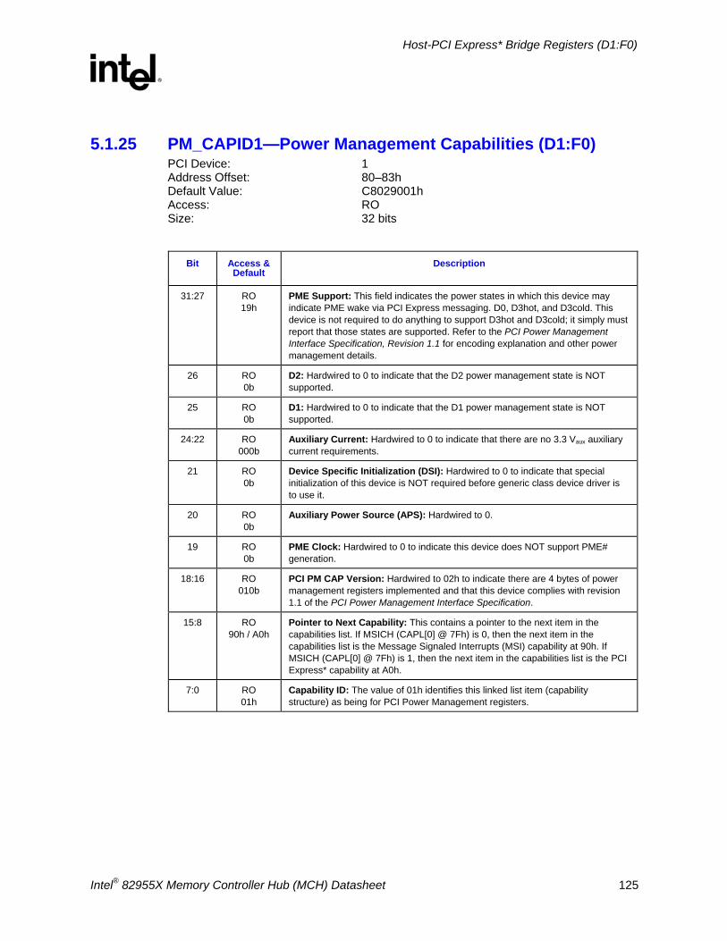
Host-PCI Express* Bridge Registers (D1:F0)
R
Intel® 82955X Memory Controller Hub (MCH) Datasheet 125
5.1.25 PM_CAPID1—Power Management Capabilities (D1:F0) PCI Device: 1 Address Offset: 80–83h Default Value: C8029001h Access: RO Size: 32 bits
Bit Access &
Default Description
31:27 RO 19h
PME Support: This field indicates the power states in which this device may indicate PME wake via PCI Express messaging. D0, D3hot, and D3cold. This device is not required to do anything to support D3hot and D3cold; it simply must report that those states are supported. Refer to the PCI Power Management Interface Specification, Revision 1.1 for encoding explanation and other power management details.
26 RO 0b
D2: Hardwired to 0 to indicate that the D2 power management state is NOT supported.
25 RO 0b
D1: Hardwired to 0 to indicate that the D1 power management state is NOT supported.
24:22 RO 000b
Auxiliary Current: Hardwired to 0 to indicate that there are no 3.3 Vaux auxiliary current requirements.
21 RO 0b
Device Specific Initialization (DSI): Hardwired to 0 to indicate that special initialization of this device is NOT required before generic class device driver is to use it.
20 RO 0b
Auxiliary Power Source (APS): Hardwired to 0.
19 RO 0b
PME Clock: Hardwired to 0 to indicate this device does NOT support PME# generation.
18:16 RO 010b
PCI PM CAP Version: Hardwired to 02h to indicate there are 4 bytes of power management registers implemented and that this device complies with revision 1.1 of the PCI Power Management Interface Specification.
15:8 RO 90h / A0h
Pointer to Next Capability: This contains a pointer to the next item in the capabilities list. If MSICH (CAPL[0] @ 7Fh) is 0, then the next item in the capabilities list is the Message Signaled Interrupts (MSI) capability at 90h. If MSICH (CAPL[0] @ 7Fh) is 1, then the next item in the capabilities list is the PCI Express* capability at A0h.
7:0 RO 01h
Capability ID: The value of 01h identifies this linked list item (capability structure) as being for PCI Power Management registers.
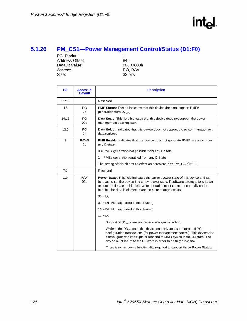
Host-PCI Express* Bridge Registers (D1:F0)
R
126 Intel® 82955X Memory Controller Hub (MCH) Datasheet
5.1.26 PM_CS1—Power Management Control/Status (D1:F0) PCI Device: 1 Address Offset: 84h Default Value: 00000000h Access: RO, R/W Size: 32 bits
Bit Access &
Default Description
31:16 Reserved
15 RO 0b
PME Status: This bit indicates that this device does not support PME# generation from D3cold.
14:13 RO 00b
Data Scale: This field indicates that this device does not support the power management data register.
12:9 RO 0h
Data Select: Indicates that this device does not support the power management data register.
8 R/W/S 0b
PME Enable: Indicates that this device does not generate PME# assertion from any D-state.
0 = PME# generation not possible from any D State
1 = PME# generation enabled from any D State
The setting of this bit has no effect on hardware. See PM_CAP[15:11]
7:2 Reserved
1:0 R/W 00b
Power State: This field indicates the current power state of this device and can be used to set the device into a new power state. If software attempts to write an unsupported state to this field, write operation must complete normally on the bus, but the data is discarded and no state change occurs.
00 = D0
01 = D1 (Not supported in this device.)
10 = D2 (Not supported in this device.)
11 = D3
Support of D3cold does not require any special action.
While in the D3hot state, this device can only act as the target of PCI configuration transactions (for power management control). This device also cannot generate interrupts or respond to MMR cycles in the D3 state. The device must return to the D0 state in order to be fully functional.
There is no hardware functionality required to support these Power States.
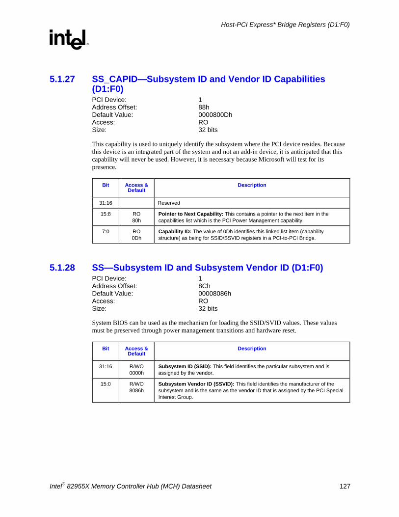
Host-PCI Express* Bridge Registers (D1:F0)
R
Intel® 82955X Memory Controller Hub (MCH) Datasheet 127
5.1.27 SS_CAPID—Subsystem ID and Vendor ID Capabilities (D1:F0) PCI Device: 1 Address Offset: 88h Default Value: 0000800Dh Access: RO Size: 32 bits
This capability is used to uniquely identify the subsystem where the PCI device resides. Because this device is an integrated part of the system and not an add-in device, it is anticipated that this capability will never be used. However, it is necessary because Microsoft will test for its presence.
Bit Access & Default
Description
31:16 Reserved
15:8 RO 80h
Pointer to Next Capability: This contains a pointer to the next item in the capabilities list which is the PCI Power Management capability.
7:0 RO 0Dh
Capability ID: The value of 0Dh identifies this linked list item (capability structure) as being for SSID/SSVID registers in a PCI-to-PCI Bridge.
5.1.28 SS—Subsystem ID and Subsystem Vendor ID (D1:F0) PCI Device: 1 Address Offset: 8Ch Default Value: 00008086h Access: RO Size: 32 bits
System BIOS can be used as the mechanism for loading the SSID/SVID values. These values must be preserved through power management transitions and hardware reset.
Bit Access & Default
Description
31:16 R/WO 0000h
Subsystem ID (SSID): This field identifies the particular subsystem and is assigned by the vendor.
15:0 R/WO 8086h
Subsystem Vendor ID (SSVID): This field identifies the manufacturer of the subsystem and is the same as the vendor ID that is assigned by the PCI Special Interest Group.
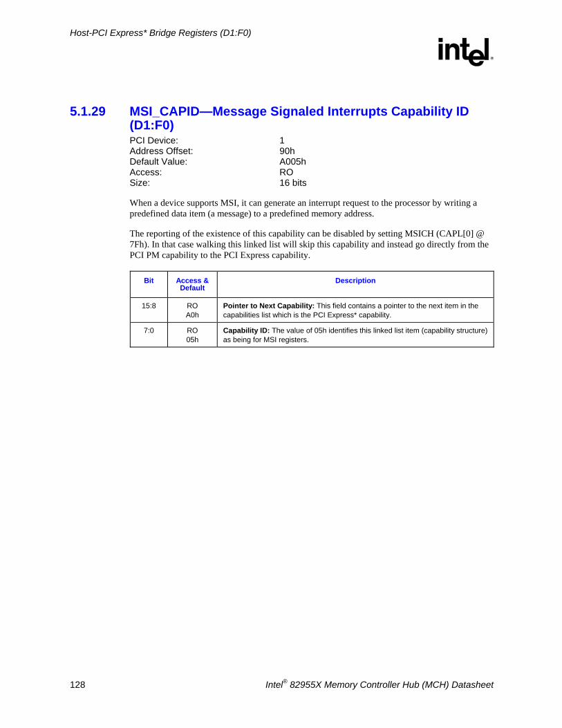
Host-PCI Express* Bridge Registers (D1:F0)
R
128 Intel® 82955X Memory Controller Hub (MCH) Datasheet
5.1.29 MSI_CAPID—Message Signaled Interrupts Capability ID (D1:F0) PCI Device: 1 Address Offset: 90h Default Value: A005h Access: RO Size: 16 bits
When a device supports MSI, it can generate an interrupt request to the processor by writing a predefined data item (a message) to a predefined memory address.
The reporting of the existence of this capability can be disabled by setting MSICH (CAPL[0] @ 7Fh). In that case walking this linked list will skip this capability and instead go directly from the PCI PM capability to the PCI Express capability.
Bit Access & Default
Description
15:8 RO A0h
Pointer to Next Capability: This field contains a pointer to the next item in the capabilities list which is the PCI Express* capability.
7:0 RO 05h
Capability ID: The value of 05h identifies this linked list item (capability structure) as being for MSI registers.
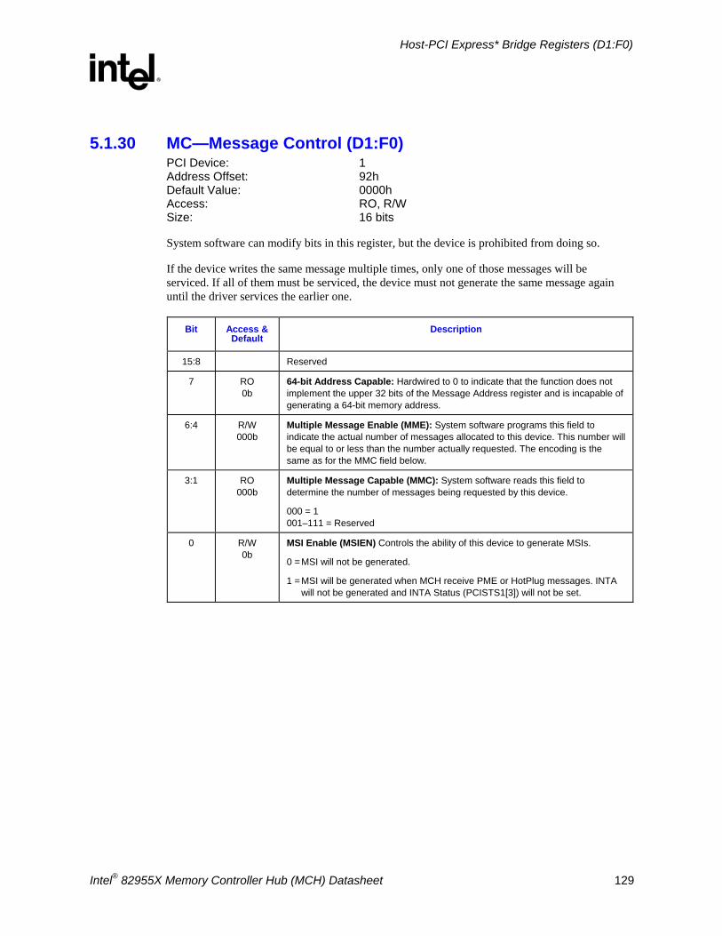
Host-PCI Express* Bridge Registers (D1:F0)
R
Intel® 82955X Memory Controller Hub (MCH) Datasheet 129
5.1.30 MC—Message Control (D1:F0) PCI Device: 1 Address Offset: 92h Default Value: 0000h Access: RO, R/W Size: 16 bits
System software can modify bits in this register, but the device is prohibited from doing so.
If the device writes the same message multiple times, only one of those messages will be serviced. If all of them must be serviced, the device must not generate the same message again until the driver services the earlier one.
Bit Access & Default
Description
15:8 Reserved
7 RO 0b
64-bit Address Capable: Hardwired to 0 to indicate that the function does not implement the upper 32 bits of the Message Address register and is incapable of generating a 64-bit memory address.
6:4 R/W 000b
Multiple Message Enable (MME): System software programs this field to indicate the actual number of messages allocated to this device. This number will be equal to or less than the number actually requested. The encoding is the same as for the MMC field below.
3:1 RO 000b
Multiple Message Capable (MMC): System software reads this field to determine the number of messages being requested by this device.
000 = 1 001–111 = Reserved
0 R/W 0b
MSI Enable (MSIEN) Controls the ability of this device to generate MSIs.
0 = MSI will not be generated.
1 = MSI will be generated when MCH receive PME or HotPlug messages. INTA will not be generated and INTA Status (PCISTS1[3]) will not be set.
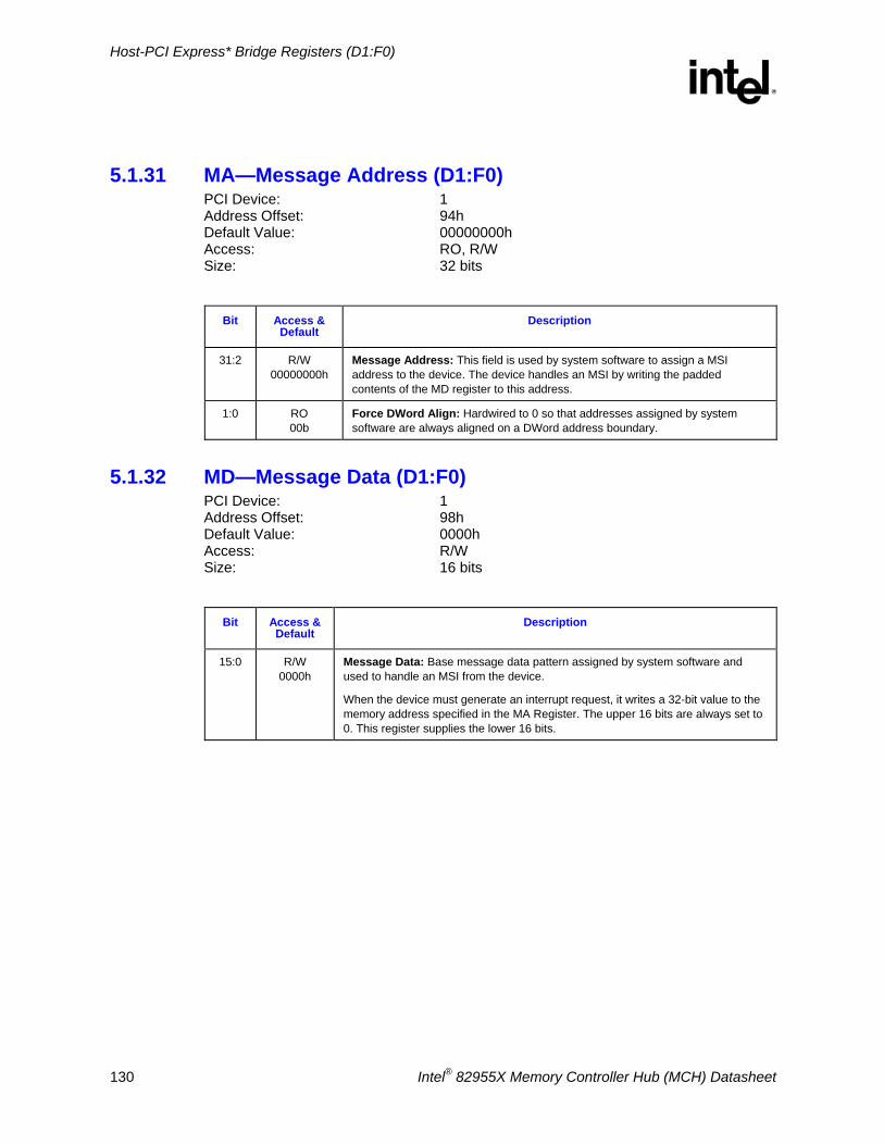
Host-PCI Express* Bridge Registers (D1:F0)
R
130 Intel® 82955X Memory Controller Hub (MCH) Datasheet
5.1.31 MA—Message Address (D1:F0) PCI Device: 1 Address Offset: 94h Default Value: 00000000h Access: RO, R/W Size: 32 bits
Bit Access &
Default Description
31:2 R/W 00000000h
Message Address: This field is used by system software to assign a MSI address to the device. The device handles an MSI by writing the padded contents of the MD register to this address.
1:0 RO 00b
Force DWord Align: Hardwired to 0 so that addresses assigned by system software are always aligned on a DWord address boundary.
5.1.32 MD—Message Data (D1:F0) PCI Device: 1 Address Offset: 98h Default Value: 0000h Access: R/W Size: 16 bits
Bit Access &
Default Description
15:0 R/W 0000h
Message Data: Base message data pattern assigned by system software and used to handle an MSI from the device.
When the device must generate an interrupt request, it writes a 32-bit value to the memory address specified in the MA Register. The upper 16 bits are always set to 0. This register supplies the lower 16 bits.
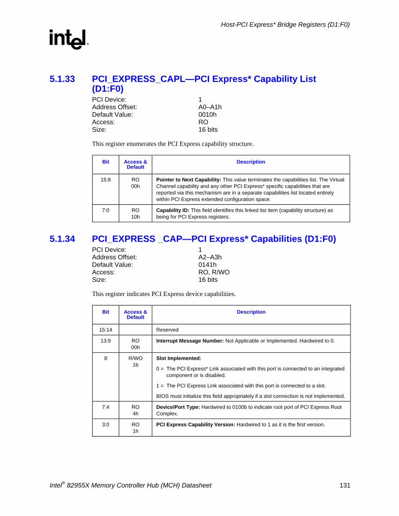
Host-PCI Express* Bridge Registers (D1:F0)
R
Intel® 82955X Memory Controller Hub (MCH) Datasheet 131
5.1.33 PCI_EXPRESS_CAPL—PCI Express* Capability List (D1:F0) PCI Device: 1 Address Offset: A0–A1h Default Value: 0010h Access: RO Size: 16 bits
This register enumerates the PCI Express capability structure.
Bit Access & Default
Description
15:8 RO 00h
Pointer to Next Capability: This value terminates the capabilities list. The Virtual Channel capability and any other PCI Express* specific capabilities that are reported via this mechanism are in a separate capabilities list located entirely within PCI Express extended configuration space.
7:0 RO 10h
Capability ID: This field identifies this linked list item (capability structure) as being for PCI Express registers.
5.1.34 PCI_EXPRESS _CAP—PCI Express* Capabilities (D1:F0) PCI Device: 1 Address Offset: A2–A3h Default Value: 0141h Access: RO, R/WO Size: 16 bits
This register indicates PCI Express device capabilities.
Bit Access & Default
Description
15:14 Reserved
13:9 RO 00h
Interrupt Message Number: Not Applicable or Implemented. Hardwired to 0.
8 R/WO 1b
Slot Implemented:
0 = The PCI Express* Link associated with this port is connected to an integrated component or is disabled.
1 = The PCI Express Link associated with this port is connected to a slot.
BIOS must initialize this field appropriately if a slot connection is not implemented.
7:4 RO 4h
Device/Port Type: Hardwired to 0100b to indicate root port of PCI Express Root Complex.
3:0 RO 1h
PCI Express Capability Version: Hardwired to 1 as it is the first version.
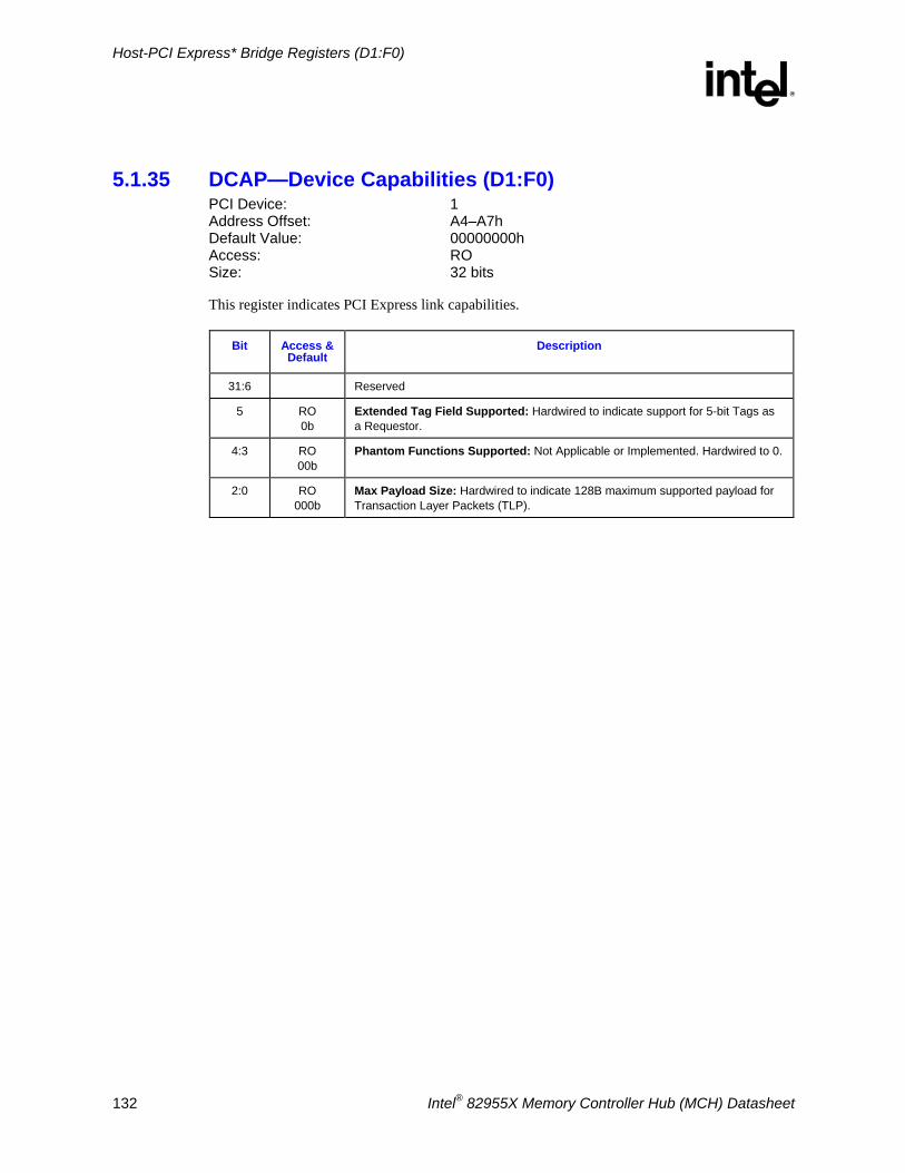
Host-PCI Express* Bridge Registers (D1:F0)
R
132 Intel® 82955X Memory Controller Hub (MCH) Datasheet
5.1.35 DCAP—Device Capabilities (D1:F0) PCI Device: 1 Address Offset: A4–A7h Default Value: 00000000h Access: RO Size: 32 bits
This register indicates PCI Express link capabilities.
Bit Access & Default
Description
31:6 Reserved
5 RO 0b
Extended Tag Field Supported: Hardwired to indicate support for 5-bit Tags as a Requestor.
4:3 RO 00b
Phantom Functions Supported: Not Applicable or Implemented. Hardwired to 0.
2:0 RO 000b
Max Payload Size: Hardwired to indicate 128B maximum supported payload for Transaction Layer Packets (TLP).
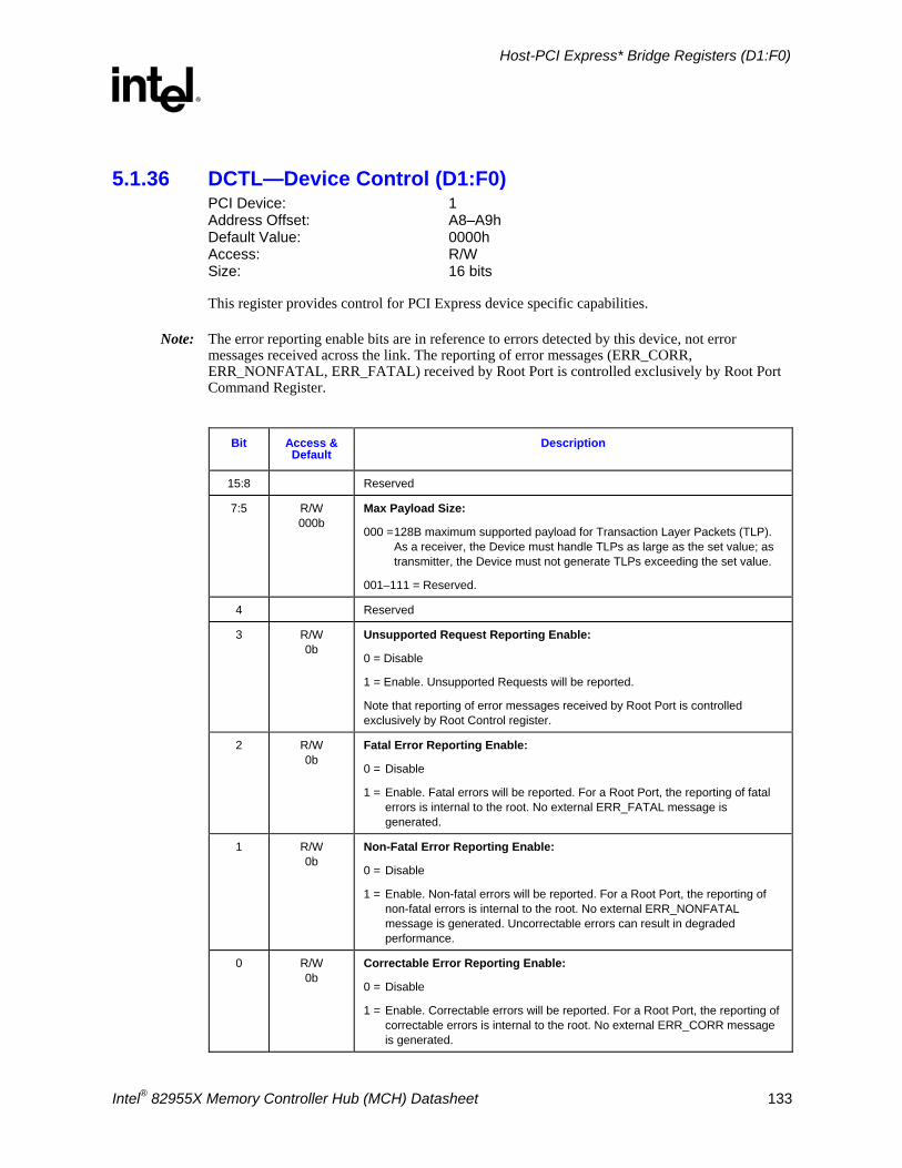
Host-PCI Express* Bridge Registers (D1:F0)
R
Intel® 82955X Memory Controller Hub (MCH) Datasheet 133
5.1.36 DCTL—Device Control (D1:F0) PCI Device: 1 Address Offset: A8–A9h Default Value: 0000h Access: R/W Size: 16 bits
This register provides control for PCI Express device specific capabilities.
Note: The error reporting enable bits are in reference to errors detected by this device, not error messages received across the link. The reporting of error messages (ERR_CORR, ERR_NONFATAL, ERR_FATAL) received by Root Port is controlled exclusively by Root Port Command Register.
Bit Access &
Default Description
15:8 Reserved
7:5 R/W 000b
Max Payload Size:
000 = 128B maximum supported payload for Transaction Layer Packets (TLP). As a receiver, the Device must handle TLPs as large as the set value; as transmitter, the Device must not generate TLPs exceeding the set value.
001–111 = Reserved.
4 Reserved
3 R/W 0b
Unsupported Request Reporting Enable:
0 = Disable
1 = Enable. Unsupported Requests will be reported.
Note that reporting of error messages received by Root Port is controlled exclusively by Root Control register.
2 R/W 0b
Fatal Error Reporting Enable:
0 = Disable
1 = Enable. Fatal errors will be reported. For a Root Port, the reporting of fatal errors is internal to the root. No external ERR_FATAL message is generated.
1 R/W 0b
Non-Fatal Error Reporting Enable:
0 = Disable
1 = Enable. Non-fatal errors will be reported. For a Root Port, the reporting of non-fatal errors is internal to the root. No external ERR_NONFATAL message is generated. Uncorrectable errors can result in degraded performance.
0 R/W 0b
Correctable Error Reporting Enable:
0 = Disable
1 = Enable. Correctable errors will be reported. For a Root Port, the reporting of correctable errors is internal to the root. No external ERR_CORR message is generated.
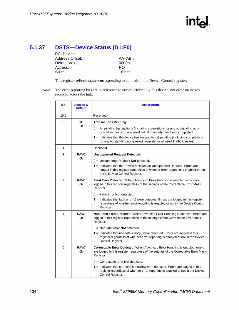
Host-PCI Express* Bridge Registers (D1:F0)
R
134 Intel® 82955X Memory Controller Hub (MCH) Datasheet
5.1.37 DSTS—Device Status (D1:F0) PCI Device: 1 Address Offset: AA–ABh Default Value: 0000h Access: RO Size: 16 bits
This register reflects status corresponding to controls in the Device Control register.
Note: The error reporting bits are in reference to errors detected by this device, not error messages received across the link.
Bit Access & Default
Description
15:6 Reserved
5 RO 0b
Transactions Pending:
0 = All pending transactions (including completions for any outstanding non-posted requests on any used virtual channel) have been completed.
1 = Indicates that the device has transaction(s) pending (including completions for any outstanding non-posted requests for all used Traffic Classes).
4 Reserved
3 R/WC 0b
Unsupported Request Detected:
0 = Unsupported Request Not detected. 1 = Indicates that the Device received an Unsupported Request. Errors are
logged in this register regardless of whether error reporting is enabled or not in the Device Control Register.
2 R/WC 0b
Fatal Error Detected: When Advanced Error Handling is enabled, errors are logged in this register regardless of the settings of the Correctable Error Mask Register.
0 = Fatal Error Not detected. 1 = Indicates that fatal error(s) were detected. Errors are logged in this register
regardless of whether error reporting is enabled or not in the Device Control Register.
1 R/WC 0b
Non-Fatal Error Detected: When Advanced Error Handling is enabled, errors are logged in this register regardless of the settings of the Correctable Error Mask Register.
0 = Non-fatal error Not detected. 1 = Indicates that non-fatal error(s) were detected. Errors are logged in this
register regardless of whether error reporting is enabled or not in the Device Control Register.
0 R/WC 0b
Correctable Error Detected: When Advanced Error Handling is enabled, errors are logged in this register regardless of the settings of the Correctable Error Mask Register.
0 = Correctable error Not detected. 1 = Indicates that correctable error(s) were detected. Errors are logged in this
register regardless of whether error reporting is enabled or not in the Device Control Register.
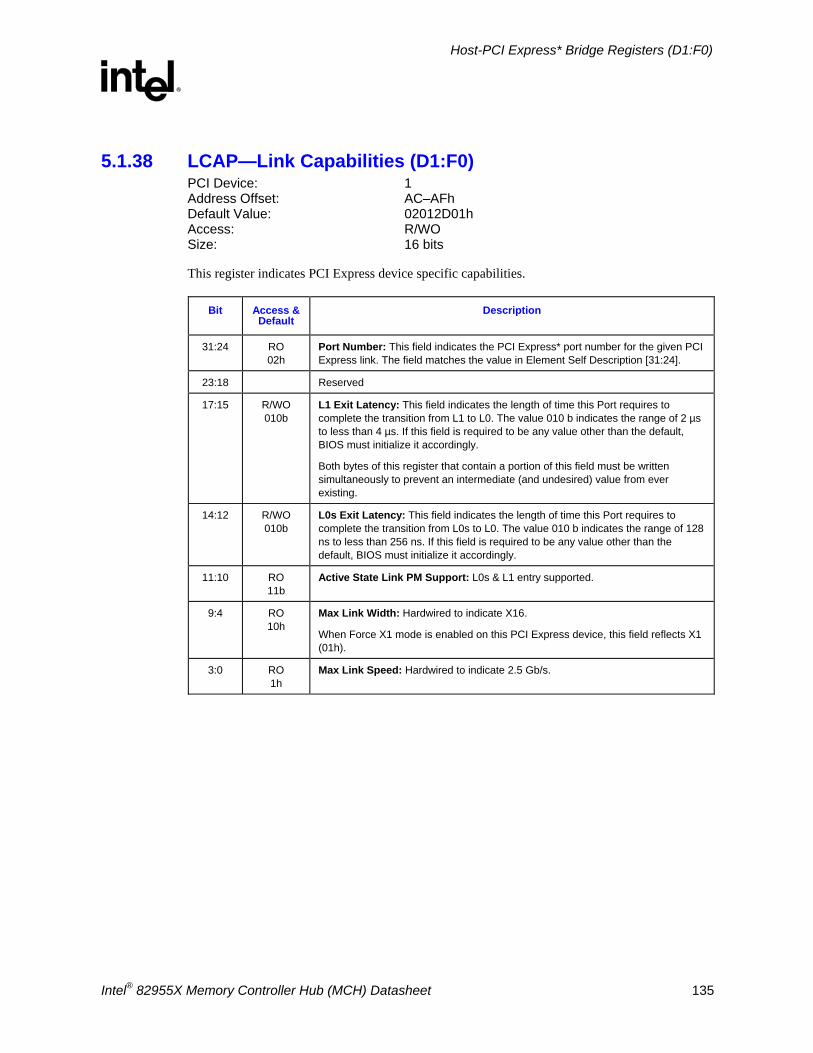
Host-PCI Express* Bridge Registers (D1:F0)
R
Intel® 82955X Memory Controller Hub (MCH) Datasheet 135
5.1.38 LCAP—Link Capabilities (D1:F0) PCI Device: 1 Address Offset: AC–AFh Default Value: 02012D01h Access: R/WO Size: 16 bits
This register indicates PCI Express device specific capabilities.
Bit Access & Default
Description
31:24 RO 02h
Port Number: This field indicates the PCI Express* port number for the given PCI Express link. The field matches the value in Element Self Description [31:24].
23:18 Reserved
17:15 R/WO 010b
L1 Exit Latency: This field indicates the length of time this Port requires to complete the transition from L1 to L0. The value 010 b indicates the range of 2 µs to less than 4 µs. If this field is required to be any value other than the default, BIOS must initialize it accordingly.
Both bytes of this register that contain a portion of this field must be written simultaneously to prevent an intermediate (and undesired) value from ever existing.
14:12 R/WO 010b
L0s Exit Latency: This field indicates the length of time this Port requires to complete the transition from L0s to L0. The value 010 b indicates the range of 128 ns to less than 256 ns. If this field is required to be any value other than the default, BIOS must initialize it accordingly.
11:10 RO 11b
Active State Link PM Support: L0s & L1 entry supported.
9:4 RO 10h
Max Link Width: Hardwired to indicate X16.
When Force X1 mode is enabled on this PCI Express device, this field reflects X1 (01h).
3:0 RO 1h
Max Link Speed: Hardwired to indicate 2.5 Gb/s.
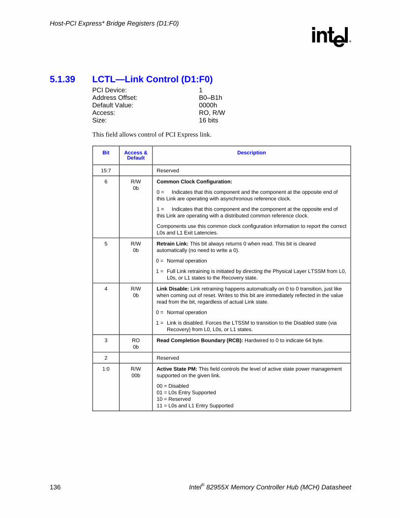
Host-PCI Express* Bridge Registers (D1:F0)
R
136 Intel® 82955X Memory Controller Hub (MCH) Datasheet
5.1.39 LCTL—Link Control (D1:F0) PCI Device: 1 Address Offset: B0–B1h Default Value: 0000h Access: RO, R/W Size: 16 bits
This field allows control of PCI Express link.
Bit Access & Default
Description
15:7 Reserved
6 R/W 0b
Common Clock Configuration:
0 = Indicates that this component and the component at the opposite end of this Link are operating with asynchronous reference clock.
1 = Indicates that this component and the component at the opposite end of this Link are operating with a distributed common reference clock.
Components use this common clock configuration information to report the correct L0s and L1 Exit Latencies.
5 R/W 0b
Retrain Link: This bit always returns 0 when read. This bit is cleared automatically (no need to write a 0).
0 = Normal operation
1 = Full Link retraining is initiated by directing the Physical Layer LTSSM from L0, L0s, or L1 states to the Recovery state.
4 R/W 0b
Link Disable: Link retraining happens automatically on 0 to 0 transition, just like when coming out of reset. Writes to this bit are immediately reflected in the value read from the bit, regardless of actual Link state.
0 = Normal operation
1 = Link is disabled. Forces the LTSSM to transition to the Disabled state (via Recovery) from L0, L0s, or L1 states.
3 RO 0b
Read Completion Boundary (RCB): Hardwired to 0 to indicate 64 byte.
2 Reserved
1:0 R/W 00b
Active State PM: This field controls the level of active state power management supported on the given link.
00 = Disabled 01 = L0s Entry Supported 10 = Reserved 11 = L0s and L1 Entry Supported
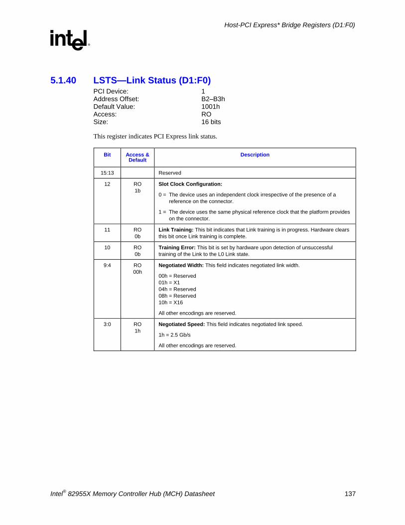
Host-PCI Express* Bridge Registers (D1:F0)
R
Intel® 82955X Memory Controller Hub (MCH) Datasheet 137
5.1.40 LSTS—Link Status (D1:F0) PCI Device: 1 Address Offset: B2–B3h Default Value: 1001h Access: RO Size: 16 bits
This register indicates PCI Express link status.
Bit Access & Default
Description
15:13 Reserved
12 RO 1b
Slot Clock Configuration:
0 = The device uses an independent clock irrespective of the presence of a reference on the connector.
1 = The device uses the same physical reference clock that the platform provides on the connector.
11 RO 0b
Link Training: This bit indicates that Link training is in progress. Hardware clears this bit once Link training is complete.
10 RO 0b
Training Error: This bit is set by hardware upon detection of unsuccessful training of the Link to the L0 Link state.
9:4 RO 00h
Negotiated Width: This field indicates negotiated link width.
00h = Reserved 01h = X1 04h = Reserved 08h = Reserved 10h = X16
All other encodings are reserved.
3:0 RO 1h
Negotiated Speed: This field indicates negotiated link speed.
1h = 2.5 Gb/s
All other encodings are reserved.
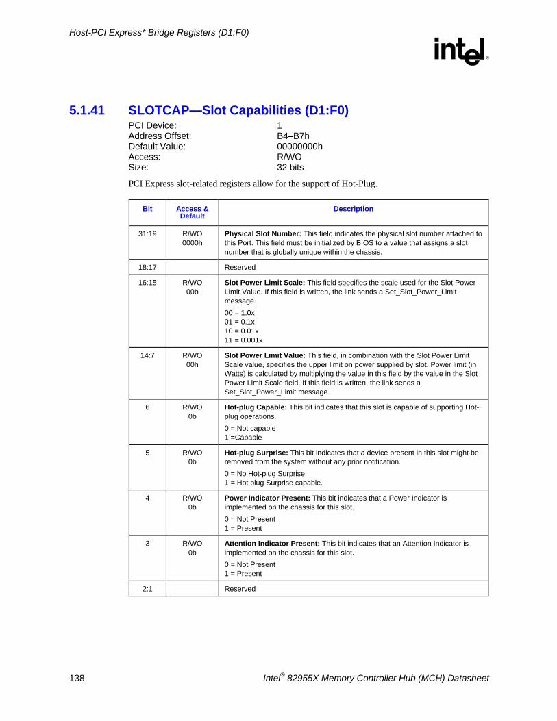
Host-PCI Express* Bridge Registers (D1:F0)
R
138 Intel® 82955X Memory Controller Hub (MCH) Datasheet
5.1.41 SLOTCAP—Slot Capabilities (D1:F0) PCI Device: 1 Address Offset: B4–B7h Default Value: 00000000h Access: R/WO Size: 32 bits
PCI Express slot-related registers allow for the support of Hot-Plug.
Bit Access & Default
Description
31:19 R/WO 0000h
Physical Slot Number: This field indicates the physical slot number attached to this Port. This field must be initialized by BIOS to a value that assigns a slot number that is globally unique within the chassis.
18:17 Reserved
16:15 R/WO 00b
Slot Power Limit Scale: This field specifies the scale used for the Slot Power Limit Value. If this field is written, the link sends a Set_Slot_Power_Limit message. 00 = 1.0x 01 = 0.1x 10 = 0.01x 11 = 0.001x
14:7 R/WO 00h
Slot Power Limit Value: This field, in combination with the Slot Power Limit Scale value, specifies the upper limit on power supplied by slot. Power limit (in Watts) is calculated by multiplying the value in this field by the value in the Slot Power Limit Scale field. If this field is written, the link sends a Set_Slot_Power_Limit message.
6 R/WO 0b
Hot-plug Capable: This bit indicates that this slot is capable of supporting Hot-plug operations. 0 = Not capable 1 =Capable
5 R/WO 0b
Hot-plug Surprise: This bit indicates that a device present in this slot might be removed from the system without any prior notification. 0 = No Hot-plug Surprise 1 = Hot plug Surprise capable.
4 R/WO 0b
Power Indicator Present: This bit indicates that a Power Indicator is implemented on the chassis for this slot. 0 = Not Present 1 = Present
3 R/WO 0b
Attention Indicator Present: This bit indicates that an Attention Indicator is implemented on the chassis for this slot. 0 = Not Present 1 = Present
2:1 Reserved
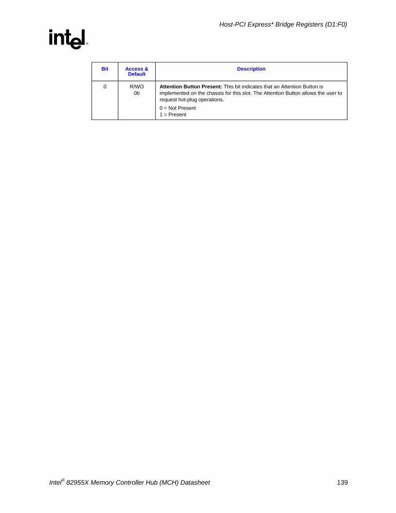
Host-PCI Express* Bridge Registers (D1:F0)
R
Intel® 82955X Memory Controller Hub (MCH) Datasheet 139
Bit Access & Default
Description
0 R/WO 0b
Attention Button Present: This bit indicates that an Attention Button is implemented on the chassis for this slot. The Attention Button allows the user to request hot-plug operations. 0 = Not Present 1 = Present
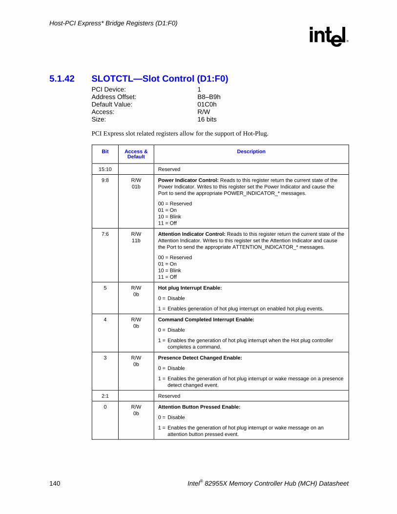
Host-PCI Express* Bridge Registers (D1:F0)
R
140 Intel® 82955X Memory Controller Hub (MCH) Datasheet
5.1.42 SLOTCTL—Slot Control (D1:F0) PCI Device: 1 Address Offset: B8–B9h Default Value: 01C0h Access: R/W Size: 16 bits
PCI Express slot related registers allow for the support of Hot-Plug.
Bit Access & Default
Description
15:10 Reserved
9:8 R/W 01b
Power Indicator Control: Reads to this register return the current state of the Power Indicator. Writes to this register set the Power Indicator and cause the Port to send the appropriate POWER_INDICATOR_* messages.
00 = Reserved 01 = On 10 = Blink 11 = Off
7:6 R/W 11b
Attention Indicator Control: Reads to this register return the current state of the Attention Indicator. Writes to this register set the Attention Indicator and cause the Port to send the appropriate ATTENTION_INDICATOR_* messages.
00 = Reserved 01 = On 10 = Blink 11 = Off
5 R/W 0b
Hot plug Interrupt Enable:
0 = Disable
1 = Enables generation of hot plug interrupt on enabled hot plug events.
4 R/W 0b
Command Completed Interrupt Enable:
0 = Disable
1 = Enables the generation of hot plug interrupt when the Hot plug controller completes a command.
3 R/W 0b
Presence Detect Changed Enable:
0 = Disable
1 = Enables the generation of hot plug interrupt or wake message on a presence detect changed event.
2:1 Reserved
0 R/W 0b
Attention Button Pressed Enable:
0 = Disable
1 = Enables the generation of hot plug interrupt or wake message on an attention button pressed event.
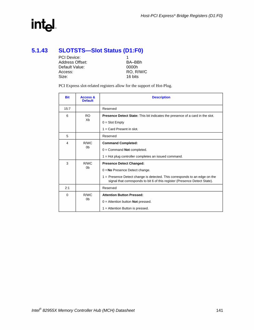
Host-PCI Express* Bridge Registers (D1:F0)
R
Intel® 82955X Memory Controller Hub (MCH) Datasheet 141
5.1.43 SLOTSTS—Slot Status (D1:F0) PCI Device: 1 Address Offset: BA–BBh Default Value: 0000h Access: RO, R/W/C Size: 16 bits
PCI Express slot-related registers allow for the support of Hot-Plug.
Bit Access & Default
Description
15:7 Reserved
6 RO Xb
Presence Detect State: This bit indicates the presence of a card in the slot.
0 = Slot Empty
1 = Card Present in slot.
5 Reserved
4 R/WC 0b
Command Completed:
0 = Command Not completed.
1 = Hot plug controller completes an issued command.
3 R/WC 0b
Presence Detect Changed:
0 = No Presence Detect change.
1 = Presence Detect change is detected. This corresponds to an edge on the signal that corresponds to bit 6 of this register (Presence Detect State).
2:1 Reserved
0 R/WC 0b
Attention Button Pressed:
0 = Attention button Not pressed.
1 = Attention Button is pressed.
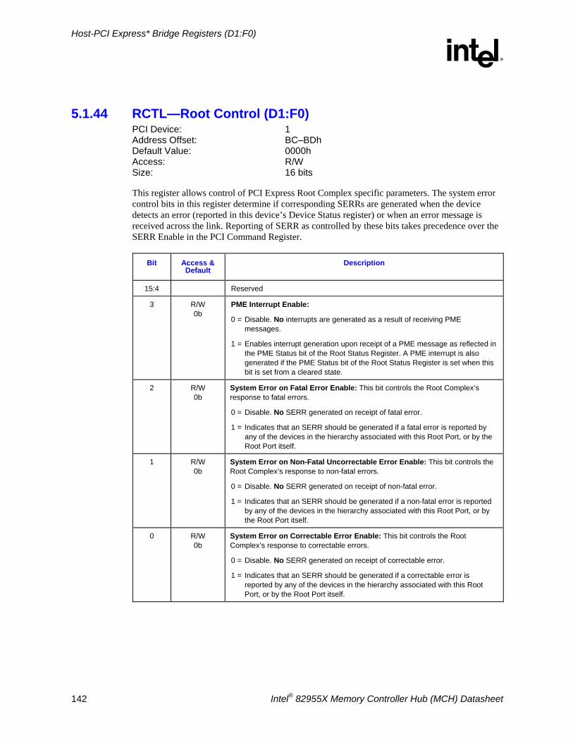
Host-PCI Express* Bridge Registers (D1:F0)
R
142 Intel® 82955X Memory Controller Hub (MCH) Datasheet
5.1.44 RCTL—Root Control (D1:F0) PCI Device: 1 Address Offset: BC–BDh Default Value: 0000h Access: R/W Size: 16 bits
This register allows control of PCI Express Root Complex specific parameters. The system error control bits in this register determine if corresponding SERRs are generated when the device detects an error (reported in this device’s Device Status register) or when an error message is received across the link. Reporting of SERR as controlled by these bits takes precedence over the SERR Enable in the PCI Command Register.
Bit Access & Default
Description
15:4 Reserved
3 R/W 0b
PME Interrupt Enable:
0 = Disable. No interrupts are generated as a result of receiving PME messages.
1 = Enables interrupt generation upon receipt of a PME message as reflected in the PME Status bit of the Root Status Register. A PME interrupt is also generated if the PME Status bit of the Root Status Register is set when this bit is set from a cleared state.
2 R/W 0b
System Error on Fatal Error Enable: This bit controls the Root Complex’s response to fatal errors.
0 = Disable. No SERR generated on receipt of fatal error.
1 = Indicates that an SERR should be generated if a fatal error is reported by any of the devices in the hierarchy associated with this Root Port, or by the Root Port itself.
1 R/W 0b
System Error on Non-Fatal Uncorrectable Error Enable: This bit controls the Root Complex’s response to non-fatal errors.
0 = Disable. No SERR generated on receipt of non-fatal error.
1 = Indicates that an SERR should be generated if a non-fatal error is reported by any of the devices in the hierarchy associated with this Root Port, or by the Root Port itself.
0 R/W 0b
System Error on Correctable Error Enable: This bit controls the Root Complex’s response to correctable errors.
0 = Disable. No SERR generated on receipt of correctable error.
1 = Indicates that an SERR should be generated if a correctable error is reported by any of the devices in the hierarchy associated with this Root Port, or by the Root Port itself.
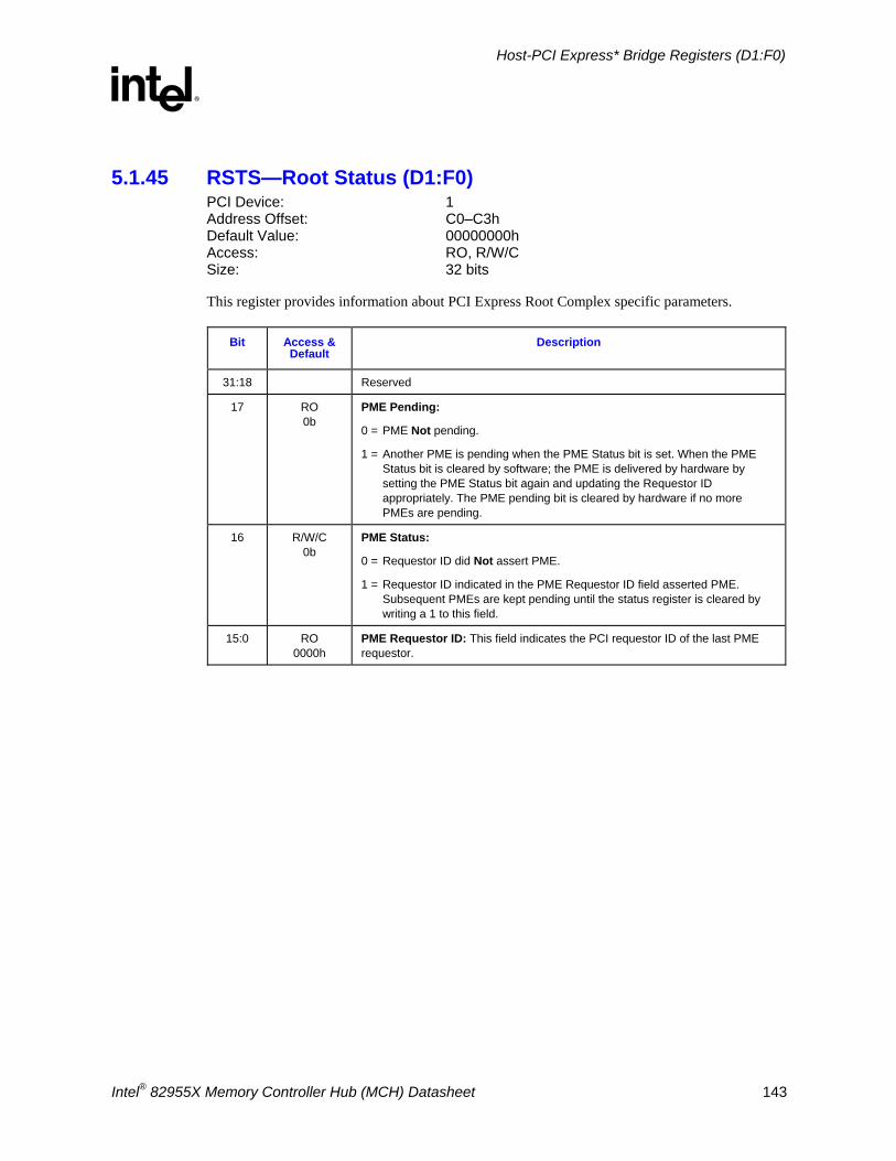
Host-PCI Express* Bridge Registers (D1:F0)
R
Intel® 82955X Memory Controller Hub (MCH) Datasheet 143
5.1.45 RSTS—Root Status (D1:F0) PCI Device: 1 Address Offset: C0–C3h Default Value: 00000000h Access: RO, R/W/C Size: 32 bits
This register provides information about PCI Express Root Complex specific parameters.
Bit Access & Default
Description
31:18 Reserved
17 RO 0b
PME Pending:
0 = PME Not pending.
1 = Another PME is pending when the PME Status bit is set. When the PME Status bit is cleared by software; the PME is delivered by hardware by setting the PME Status bit again and updating the Requestor ID appropriately. The PME pending bit is cleared by hardware if no more PMEs are pending.
16 R/W/C 0b
PME Status:
0 = Requestor ID did Not assert PME.
1 = Requestor ID indicated in the PME Requestor ID field asserted PME. Subsequent PMEs are kept pending until the status register is cleared by writing a 1 to this field.
15:0 RO 0000h
PME Requestor ID: This field indicates the PCI requestor ID of the last PME requestor.
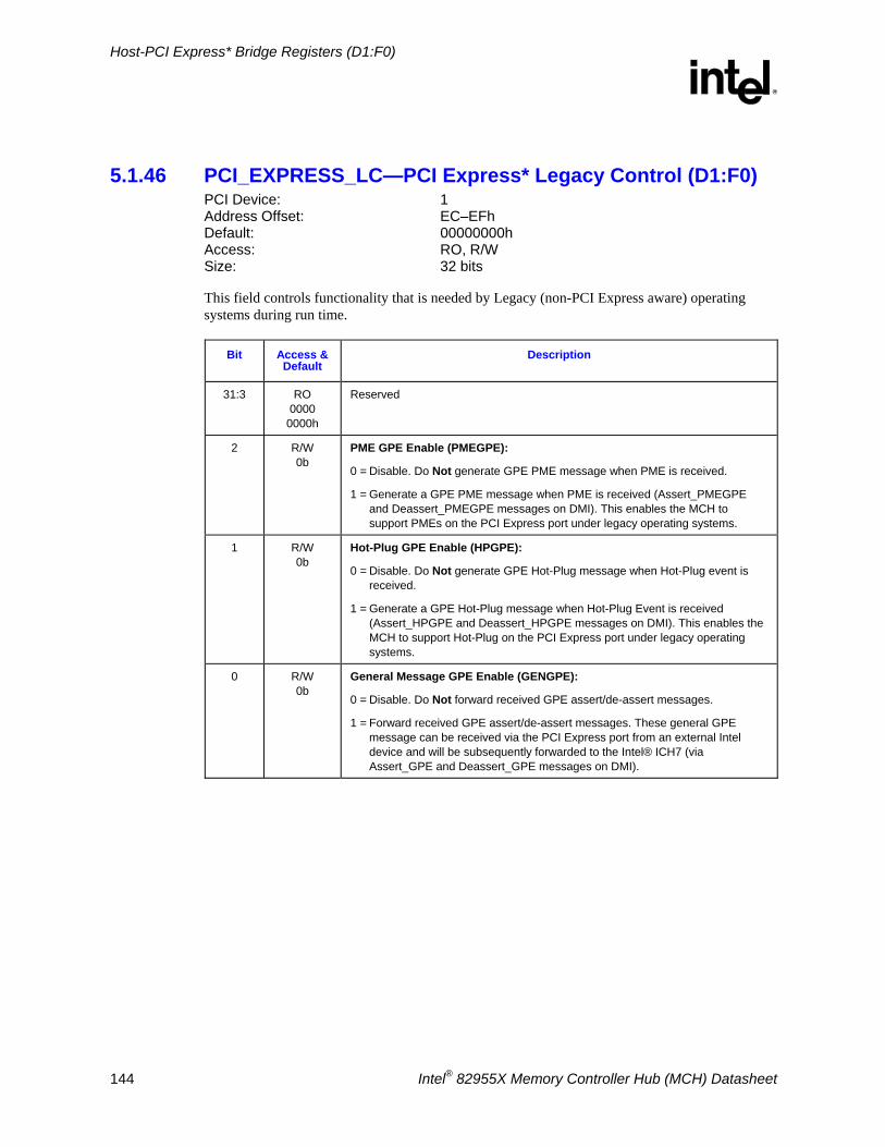
Host-PCI Express* Bridge Registers (D1:F0)
R
144 Intel® 82955X Memory Controller Hub (MCH) Datasheet
5.1.46 PCI_EXPRESS_LC—PCI Express* Legacy Control (D1:F0) PCI Device: 1 Address Offset: EC–EFh Default: 00000000h Access: RO, R/W Size: 32 bits
This field controls functionality that is needed by Legacy (non-PCI Express aware) operating systems during run time.
Bit Access & Default
Description
31:3 RO 0000 0000h
Reserved
2 R/W 0b
PME GPE Enable (PMEGPE):
0 = Disable. Do Not generate GPE PME message when PME is received.
1 = Generate a GPE PME message when PME is received (Assert_PMEGPE and Deassert_PMEGPE messages on DMI). This enables the MCH to support PMEs on the PCI Express port under legacy operating systems.
1 R/W 0b
Hot-Plug GPE Enable (HPGPE):
0 = Disable. Do Not generate GPE Hot-Plug message when Hot-Plug event is received.
1 = Generate a GPE Hot-Plug message when Hot-Plug Event is received (Assert_HPGPE and Deassert_HPGPE messages on DMI). This enables the MCH to support Hot-Plug on the PCI Express port under legacy operating systems.
0 R/W 0b
General Message GPE Enable (GENGPE):
0 = Disable. Do Not forward received GPE assert/de-assert messages.
1 = Forward received GPE assert/de-assert messages. These general GPE message can be received via the PCI Express port from an external Intel device and will be subsequently forwarded to the Intel® ICH7 (via Assert_GPE and Deassert_GPE messages on DMI).
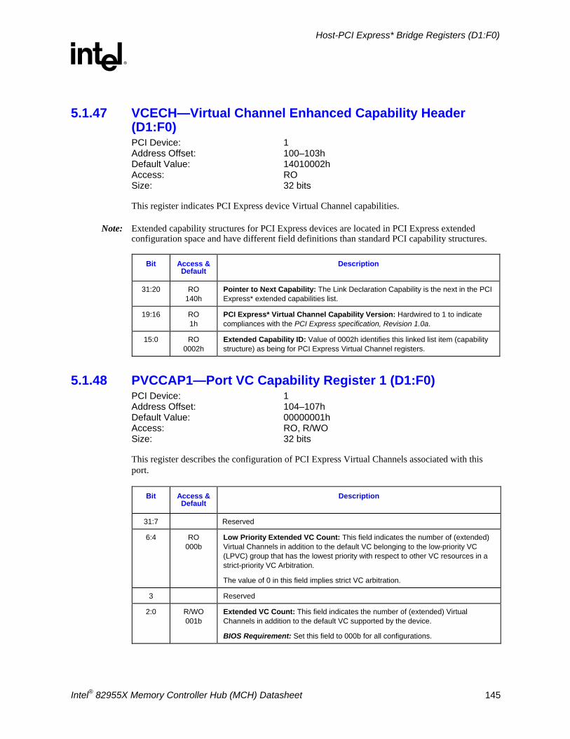
Host-PCI Express* Bridge Registers (D1:F0)
R
Intel® 82955X Memory Controller Hub (MCH) Datasheet 145
5.1.47 VCECH—Virtual Channel Enhanced Capability Header (D1:F0) PCI Device: 1 Address Offset: 100–103h Default Value: 14010002h Access: RO Size: 32 bits
This register indicates PCI Express device Virtual Channel capabilities.
Note: Extended capability structures for PCI Express devices are located in PCI Express extended configuration space and have different field definitions than standard PCI capability structures.
Bit Access & Default
Description
31:20 RO 140h
Pointer to Next Capability: The Link Declaration Capability is the next in the PCI Express* extended capabilities list.
19:16 RO 1h
PCI Express* Virtual Channel Capability Version: Hardwired to 1 to indicate compliances with the PCI Express specification, Revision 1.0a.
15:0 RO 0002h
Extended Capability ID: Value of 0002h identifies this linked list item (capability structure) as being for PCI Express Virtual Channel registers.
5.1.48 PVCCAP1—Port VC Capability Register 1 (D1:F0) PCI Device: 1 Address Offset: 104–107h Default Value: 00000001h Access: RO, R/WO Size: 32 bits
This register describes the configuration of PCI Express Virtual Channels associated with this port.
Bit Access & Default
Description
31:7 Reserved
6:4 RO 000b
Low Priority Extended VC Count: This field indicates the number of (extended) Virtual Channels in addition to the default VC belonging to the low-priority VC (LPVC) group that has the lowest priority with respect to other VC resources in a strict-priority VC Arbitration.
The value of 0 in this field implies strict VC arbitration.
3 Reserved
2:0 R/WO 001b
Extended VC Count: This field indicates the number of (extended) Virtual Channels in addition to the default VC supported by the device.
BIOS Requirement: Set this field to 000b for all configurations.
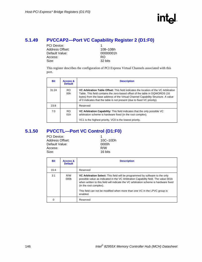
Host-PCI Express* Bridge Registers (D1:F0)
R
146 Intel® 82955X Memory Controller Hub (MCH) Datasheet
5.1.49 PVCCAP2—Port VC Capability Register 2 (D1:F0) PCI Device: 1 Address Offset: 108–10Bh Default Value: 00000001h Access: RO Size: 32 bits
This register describes the configuration of PCI Express Virtual Channels associated with this port.
Bit Access & Default
Description
31:24 RO 00h
VC Arbitration Table Offset: This field indicates the location of the VC Arbitration Table. This field contains the zero-based offset of the table in DQWORDS (16 bytes) from the base address of the Virtual Channel Capability Structure. A value of 0 indicates that the table is not present (due to fixed VC priority).
23:8 Reserved
7:0 RO 01h
VC Arbitration Capability: This field indicates that the only possible VC arbitration scheme is hardware fixed (in the root complex).
VC1 is the highest priority, VC0 is the lowest priority.
5.1.50 PVCCTL—Port VC Control (D1:F0) PCI Device: 1 Address Offset: 10C–10Dh Default Value: 0000h Access: R/W Size: 16 bits
Bit Access & Default
Description
15:4 Reserved
3:1 R/W 000b
VC Arbitration Select: This field will be programmed by software to the only possible value as indicated in the VC Arbitration Capability field. The value 001b when written to this field will indicate the VC arbitration scheme is hardware fixed (in the root complex).
This field can not be modified when more than one VC in the LPVC group is enabled.
0 Reserved
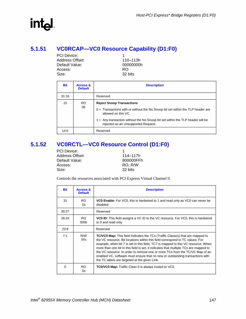
Host-PCI Express* Bridge Registers (D1:F0)
R
Intel® 82955X Memory Controller Hub (MCH) Datasheet 147
5.1.51 VC0RCAP—VC0 Resource Capability (D1:F0) PCI Device: 1 Address Offset: 110–113h Default Value: 00000000h Access: RO Size: 32 bits
Bit Access & Default
Description
31:16 Reserved
15 RO 0b
Reject Snoop Transactions
0 = Transactions with or without the No Snoop bit set within the TLP header are allowed on this VC.
1 = Any transaction without the No Snoop bit set within the TLP header will be rejected as an Unsupported Request.
14:0 Reserved
5.1.52 VC0RCTL—VC0 Resource Control (D1:F0) PCI Device: 1 Address Offset: 114–117h Default Value: 800000FFh Access: RO, R/W Size: 32 bits
Controls the resources associated with PCI Express Virtual Channel 0.
Bit Access & Default
Description
31 RO 1b
VC0 Enable: For VC0, this is hardwired to 1 and read only as VC0 can never be disabled.
30:27 Reserved
26:24 RO 000b
VC0 ID: This field assigns a VC ID to the VC resource. For VC0, this is hardwired to 0 and read only.
23:8 Reserved
7:1 R/W 7Fh
TC/VC0 Map: This field indicates the TCs (Traffic Classes) that are mapped to the VC resource. Bit locations within this field correspond to TC values. For example, when bit 7 is set in this field, TC7 is mapped to this VC resource. When more than one bit in this field is set, it indicates that multiple TCs are mapped to the VC resource. In order to remove one or more TCs from the TC/VC Map of an enabled VC, software must ensure that no new or outstanding transactions with the TC labels are targeted at the given Link.
0 RO 1b
TC0/VC0 Map: Traffic Class 0 is always routed to VC0.
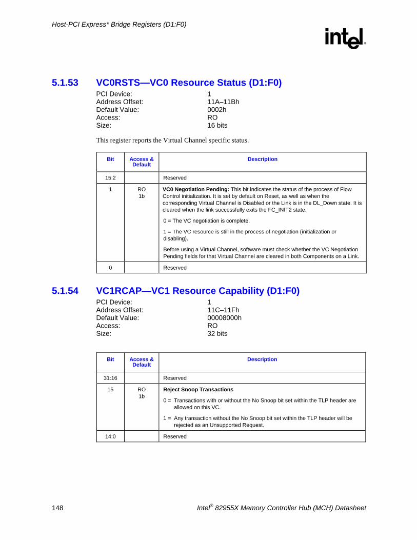
Host-PCI Express* Bridge Registers (D1:F0)
R
148 Intel® 82955X Memory Controller Hub (MCH) Datasheet
5.1.53 VC0RSTS—VC0 Resource Status (D1:F0) PCI Device: 1 Address Offset: 11A–11Bh Default Value: 0002h Access: RO Size: 16 bits
This register reports the Virtual Channel specific status.
Bit Access & Default
Description
15:2 Reserved
1 RO 1b
VC0 Negotiation Pending: This bit indicates the status of the process of Flow Control initialization. It is set by default on Reset, as well as when the corresponding Virtual Channel is Disabled or the Link is in the DL_Down state. It is cleared when the link successfully exits the FC_INIT2 state.
0 = The VC negotiation is complete.
1 = The VC resource is still in the process of negotiation (initialization or disabling).
Before using a Virtual Channel, software must check whether the VC Negotiation Pending fields for that Virtual Channel are cleared in both Components on a Link.
0 Reserved
5.1.54 VC1RCAP—VC1 Resource Capability (D1:F0) PCI Device: 1 Address Offset: 11C–11Fh Default Value: 00008000h Access: RO Size: 32 bits
Bit Access &
Default Description
31:16 Reserved
15 RO 1b
Reject Snoop Transactions
0 = Transactions with or without the No Snoop bit set within the TLP header are allowed on this VC.
1 = Any transaction without the No Snoop bit set within the TLP header will be rejected as an Unsupported Request.
14:0 Reserved
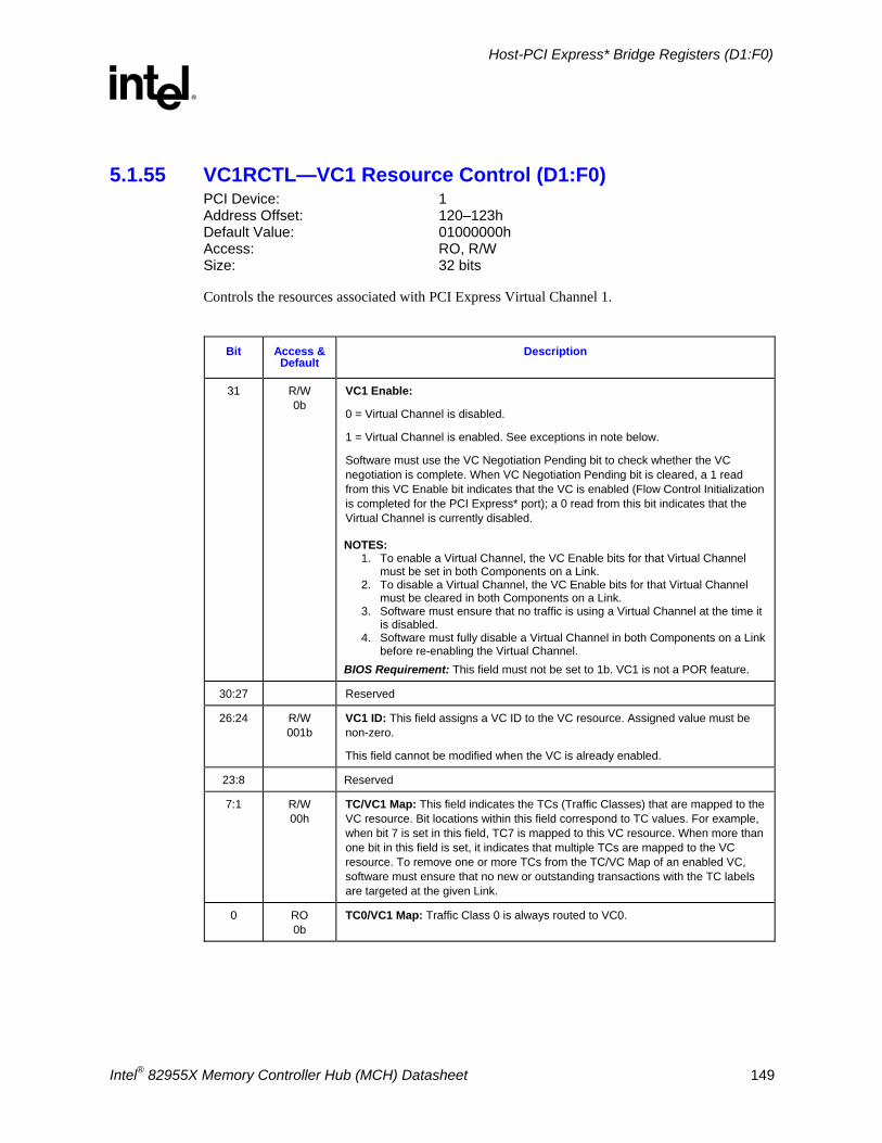
Host-PCI Express* Bridge Registers (D1:F0)
R
Intel® 82955X Memory Controller Hub (MCH) Datasheet 149
5.1.55 VC1RCTL—VC1 Resource Control (D1:F0) PCI Device: 1 Address Offset: 120–123h Default Value: 01000000h Access: RO, R/W Size: 32 bits
Controls the resources associated with PCI Express Virtual Channel 1.
Bit Access &
Default Description
31 R/W 0b
VC1 Enable:
0 = Virtual Channel is disabled.
1 = Virtual Channel is enabled. See exceptions in note below.
Software must use the VC Negotiation Pending bit to check whether the VC negotiation is complete. When VC Negotiation Pending bit is cleared, a 1 read from this VC Enable bit indicates that the VC is enabled (Flow Control Initialization is completed for the PCI Express* port); a 0 read from this bit indicates that the Virtual Channel is currently disabled.
NOTES: 1. To enable a Virtual Channel, the VC Enable bits for that Virtual Channel
must be set in both Components on a Link. 2. To disable a Virtual Channel, the VC Enable bits for that Virtual Channel
must be cleared in both Components on a Link. 3. Software must ensure that no traffic is using a Virtual Channel at the time it
is disabled. 4. Software must fully disable a Virtual Channel in both Components on a Link
before re-enabling the Virtual Channel. BIOS Requirement: This field must not be set to 1b. VC1 is not a POR feature.
30:27 Reserved
26:24 R/W 001b
VC1 ID: This field assigns a VC ID to the VC resource. Assigned value must be non-zero.
This field cannot be modified when the VC is already enabled.
23:8 Reserved
7:1 R/W 00h
TC/VC1 Map: This field indicates the TCs (Traffic Classes) that are mapped to the VC resource. Bit locations within this field correspond to TC values. For example, when bit 7 is set in this field, TC7 is mapped to this VC resource. When more than one bit in this field is set, it indicates that multiple TCs are mapped to the VC resource. To remove one or more TCs from the TC/VC Map of an enabled VC, software must ensure that no new or outstanding transactions with the TC labels are targeted at the given Link.
0 RO 0b
TC0/VC1 Map: Traffic Class 0 is always routed to VC0.
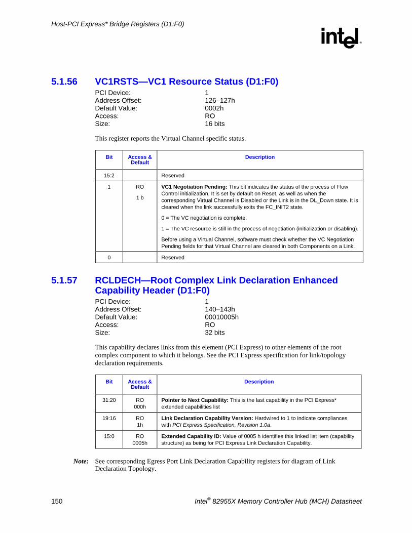
Host-PCI Express* Bridge Registers (D1:F0)
R
150 Intel® 82955X Memory Controller Hub (MCH) Datasheet
5.1.56 VC1RSTS—VC1 Resource Status (D1:F0) PCI Device: 1 Address Offset: 126–127h Default Value: 0002h Access: RO Size: 16 bits
This register reports the Virtual Channel specific status.
Bit Access & Default
Description
15:2 Reserved
1 RO
1 b
VC1 Negotiation Pending: This bit indicates the status of the process of Flow Control initialization. It is set by default on Reset, as well as when the corresponding Virtual Channel is Disabled or the Link is in the DL_Down state. It is cleared when the link successfully exits the FC_INIT2 state.
0 = The VC negotiation is complete.
1 = The VC resource is still in the process of negotiation (initialization or disabling).
Before using a Virtual Channel, software must check whether the VC Negotiation Pending fields for that Virtual Channel are cleared in both Components on a Link.
0 Reserved
5.1.57 RCLDECH—Root Complex Link Declaration Enhanced Capability Header (D1:F0) PCI Device: 1 Address Offset: 140–143h Default Value: 00010005h Access: RO Size: 32 bits
This capability declares links from this element (PCI Express) to other elements of the root complex component to which it belongs. See the PCI Express specification for link/topology declaration requirements.
Bit Access & Default
Description
31:20 RO 000h
Pointer to Next Capability: This is the last capability in the PCI Express* extended capabilities list
19:16 RO 1h
Link Declaration Capability Version: Hardwired to 1 to indicate compliances with PCI Express Specification, Revision 1.0a.
15:0 RO 0005h
Extended Capability ID: Value of 0005 h identifies this linked list item (capability structure) as being for PCI Express Link Declaration Capability.
Note: See corresponding Egress Port Link Declaration Capability registers for diagram of Link Declaration Topology.
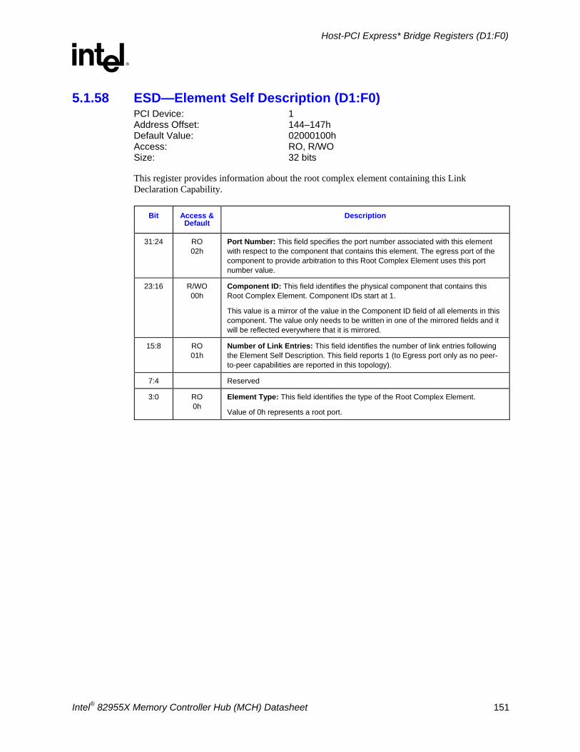
Host-PCI Express* Bridge Registers (D1:F0)
R
Intel® 82955X Memory Controller Hub (MCH) Datasheet 151
5.1.58 ESD—Element Self Description (D1:F0) PCI Device: 1 Address Offset: 144–147h Default Value: 02000100h Access: RO, R/WO Size: 32 bits
This register provides information about the root complex element containing this Link Declaration Capability.
Bit Access & Default
Description
31:24 RO 02h
Port Number: This field specifies the port number associated with this element with respect to the component that contains this element. The egress port of the component to provide arbitration to this Root Complex Element uses this port number value.
23:16 R/WO 00h
Component ID: This field identifies the physical component that contains this Root Complex Element. Component IDs start at 1.
This value is a mirror of the value in the Component ID field of all elements in this component. The value only needs to be written in one of the mirrored fields and it will be reflected everywhere that it is mirrored.
15:8 RO 01h
Number of Link Entries: This field identifies the number of link entries following the Element Self Description. This field reports 1 (to Egress port only as no peer-to-peer capabilities are reported in this topology).
7:4 Reserved
3:0 RO 0h
Element Type: This field identifies the type of the Root Complex Element.
Value of 0h represents a root port.
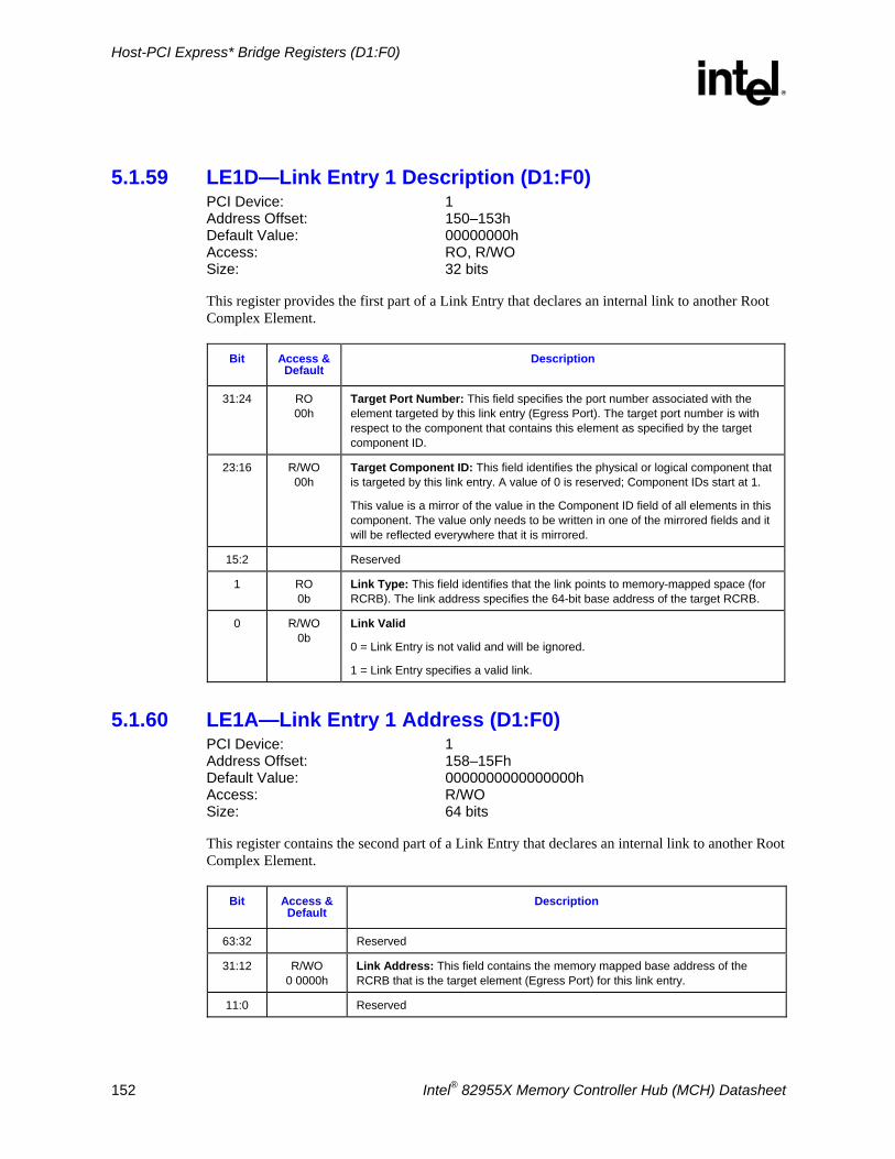
Host-PCI Express* Bridge Registers (D1:F0)
R
152 Intel® 82955X Memory Controller Hub (MCH) Datasheet
5.1.59 LE1D—Link Entry 1 Description (D1:F0) PCI Device: 1 Address Offset: 150–153h Default Value: 00000000h Access: RO, R/WO Size: 32 bits
This register provides the first part of a Link Entry that declares an internal link to another Root Complex Element.
Bit Access & Default
Description
31:24 RO 00h
Target Port Number: This field specifies the port number associated with the element targeted by this link entry (Egress Port). The target port number is with respect to the component that contains this element as specified by the target component ID.
23:16 R/WO 00h
Target Component ID: This field identifies the physical or logical component that is targeted by this link entry. A value of 0 is reserved; Component IDs start at 1.
This value is a mirror of the value in the Component ID field of all elements in this component. The value only needs to be written in one of the mirrored fields and it will be reflected everywhere that it is mirrored.
15:2 Reserved
1 RO 0b
Link Type: This field identifies that the link points to memory-mapped space (for RCRB). The link address specifies the 64-bit base address of the target RCRB.
0 R/WO 0b
Link Valid
0 = Link Entry is not valid and will be ignored.
1 = Link Entry specifies a valid link.
5.1.60 LE1A—Link Entry 1 Address (D1:F0) PCI Device: 1 Address Offset: 158–15Fh Default Value: 0000000000000000h Access: R/WO Size: 64 bits
This register contains the second part of a Link Entry that declares an internal link to another Root Complex Element.
Bit Access & Default
Description
63:32 Reserved
31:12 R/WO 0 0000h
Link Address: This field contains the memory mapped base address of the RCRB that is the target element (Egress Port) for this link entry.
11:0 Reserved
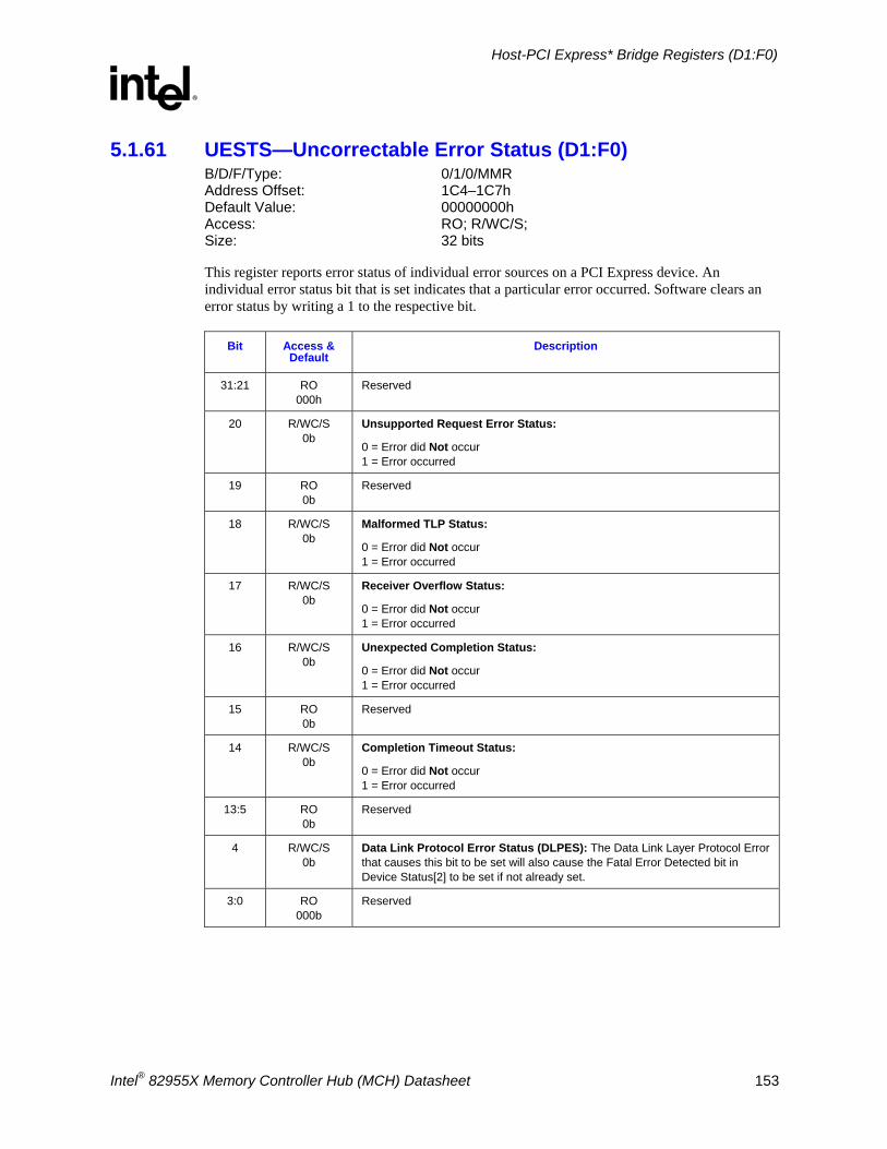
Host-PCI Express* Bridge Registers (D1:F0)
R
Intel® 82955X Memory Controller Hub (MCH) Datasheet 153
5.1.61 UESTS—Uncorrectable Error Status (D1:F0) B/D/F/Type: 0/1/0/MMR Address Offset: 1C4–1C7h Default Value: 00000000h Access: RO; R/WC/S; Size: 32 bits
This register reports error status of individual error sources on a PCI Express device. An individual error status bit that is set indicates that a particular error occurred. Software clears an error status by writing a 1 to the respective bit.
Bit Access & Default
Description
31:21 RO 000h
Reserved
20 R/WC/S 0b
Unsupported Request Error Status:
0 = Error did Not occur 1 = Error occurred
19 RO 0b
Reserved
18 R/WC/S 0b
Malformed TLP Status:
0 = Error did Not occur 1 = Error occurred
17 R/WC/S 0b
Receiver Overflow Status:
0 = Error did Not occur 1 = Error occurred
16 R/WC/S 0b
Unexpected Completion Status:
0 = Error did Not occur 1 = Error occurred
15 RO 0b
Reserved
14 R/WC/S 0b
Completion Timeout Status:
0 = Error did Not occur 1 = Error occurred
13:5 RO 0b
Reserved
4 R/WC/S 0b
Data Link Protocol Error Status (DLPES): The Data Link Layer Protocol Error that causes this bit to be set will also cause the Fatal Error Detected bit in Device Status[2] to be set if not already set.
3:0 RO 000b
Reserved
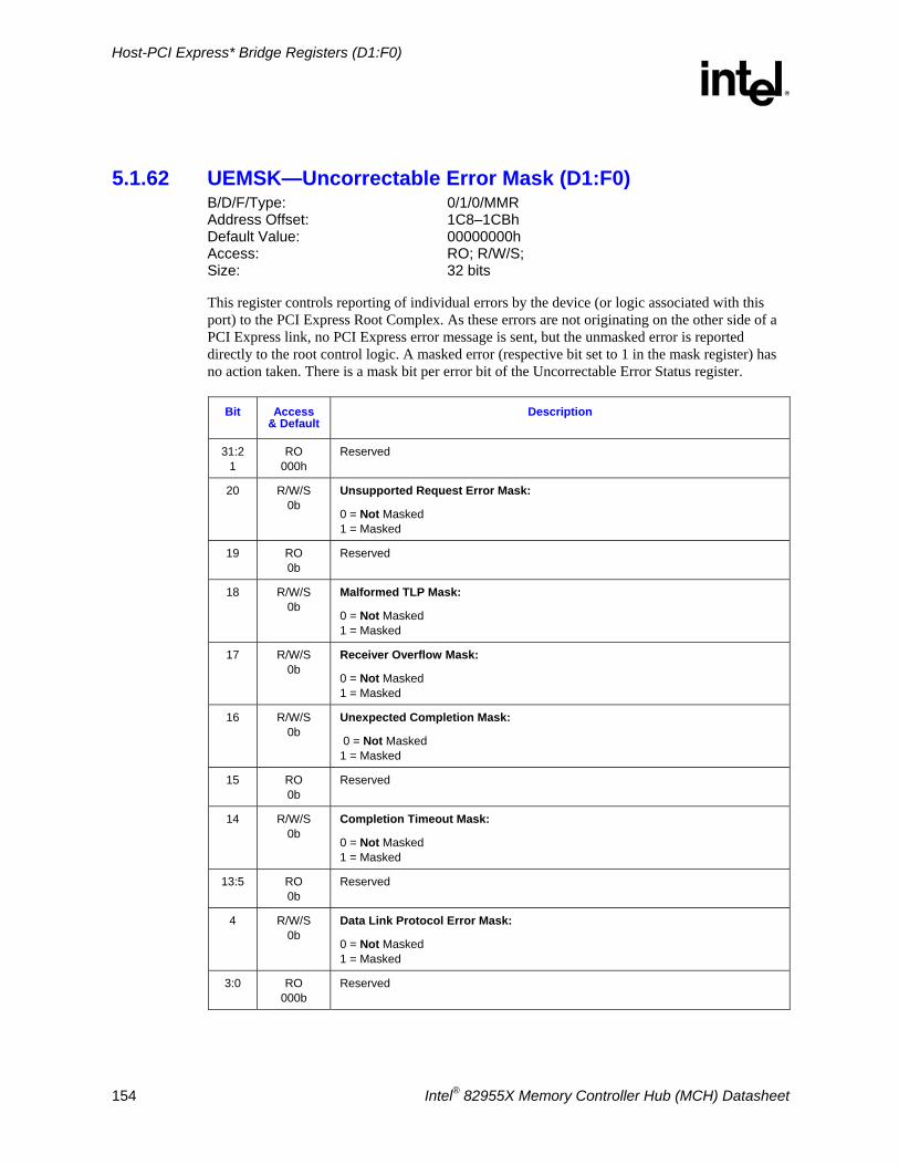
Host-PCI Express* Bridge Registers (D1:F0)
R
154 Intel® 82955X Memory Controller Hub (MCH) Datasheet
5.1.62 UEMSK—Uncorrectable Error Mask (D1:F0) B/D/F/Type: 0/1/0/MMR Address Offset: 1C8–1CBh Default Value: 00000000h Access: RO; R/W/S; Size: 32 bits
This register controls reporting of individual errors by the device (or logic associated with this port) to the PCI Express Root Complex. As these errors are not originating on the other side of a PCI Express link, no PCI Express error message is sent, but the unmasked error is reported directly to the root control logic. A masked error (respective bit set to 1 in the mask register) has no action taken. There is a mask bit per error bit of the Uncorrectable Error Status register.
Bit Access & Default
Description
31:21
RO 000h
Reserved
20 R/W/S 0b
Unsupported Request Error Mask:
0 = Not Masked 1 = Masked
19 RO 0b
Reserved
18 R/W/S 0b
Malformed TLP Mask:
0 = Not Masked 1 = Masked
17 R/W/S 0b
Receiver Overflow Mask:
0 = Not Masked 1 = Masked
16 R/W/S 0b
Unexpected Completion Mask:
0 = Not Masked 1 = Masked
15 RO 0b
Reserved
14 R/W/S 0b
Completion Timeout Mask:
0 = Not Masked 1 = Masked
13:5 RO 0b
Reserved
4 R/W/S 0b
Data Link Protocol Error Mask:
0 = Not Masked 1 = Masked
3:0 RO 000b
Reserved
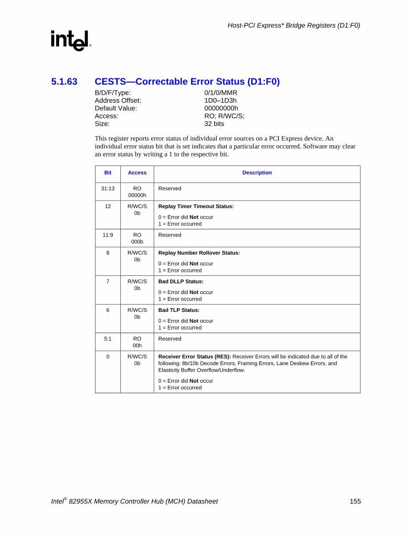
Host-PCI Express* Bridge Registers (D1:F0)
R
Intel® 82955X Memory Controller Hub (MCH) Datasheet 155
5.1.63 CESTS—Correctable Error Status (D1:F0) B/D/F/Type: 0/1/0/MMR Address Offset: 1D0–1D3h Default Value: 00000000h Access: RO; R/WC/S; Size: 32 bits
This register reports error status of individual error sources on a PCI Express device. An individual error status bit that is set indicates that a particular error occurred. Software may clear an error status by writing a 1 to the respective bit.
Bit Access Description
31:13 RO 00000h
Reserved
12 R/WC/S 0b
Replay Timer Timeout Status:
0 = Error did Not occur 1 = Error occurred
11:9 RO 000b
Reserved
8 R/WC/S 0b
Replay Number Rollover Status:
0 = Error did Not occur 1 = Error occurred
7 R/WC/S 0b
Bad DLLP Status:
0 = Error did Not occur 1 = Error occurred
6 R/WC/S 0b
Bad TLP Status:
0 = Error did Not occur 1 = Error occurred
5:1 RO 00h
Reserved
0 R/WC/S 0b
Receiver Error Status (RES): Receiver Errors will be indicated due to all of the following: 8b/10b Decode Errors, Framing Errors, Lane Deskew Errors, and Elasticity Buffer Overflow/Underflow.
0 = Error did Not occur 1 = Error occurred
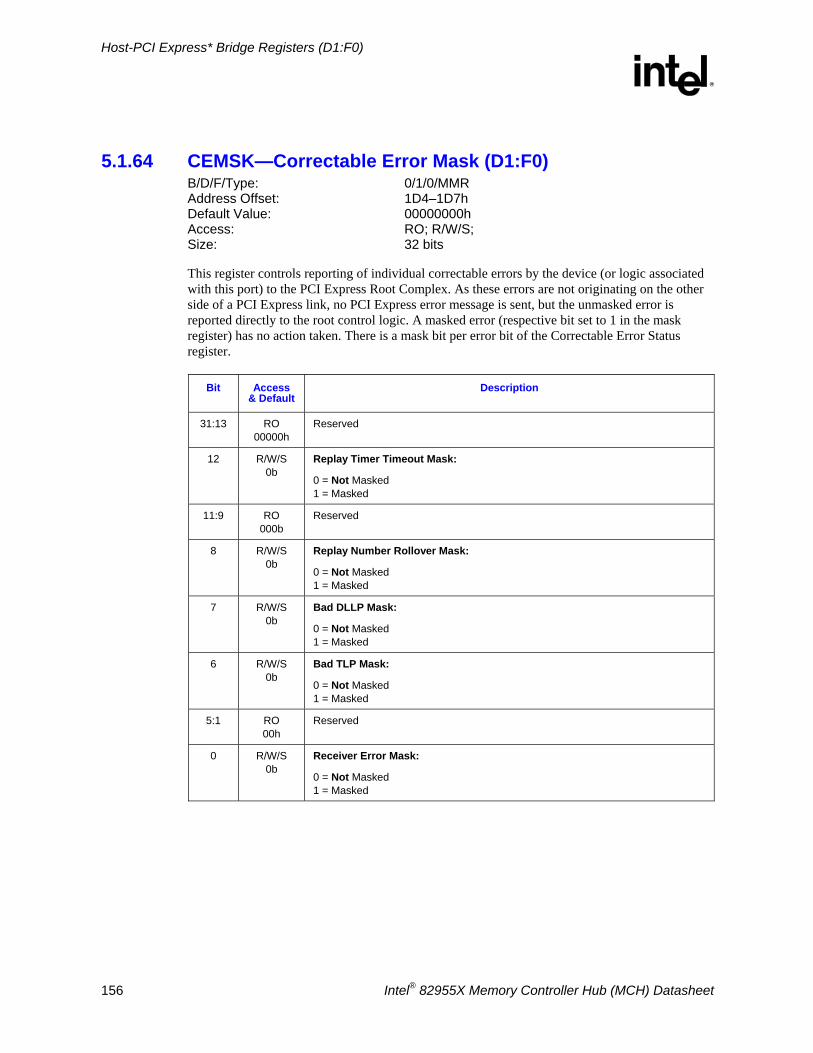
Host-PCI Express* Bridge Registers (D1:F0)
R
156 Intel® 82955X Memory Controller Hub (MCH) Datasheet
5.1.64 CEMSK—Correctable Error Mask (D1:F0) B/D/F/Type: 0/1/0/MMR Address Offset: 1D4–1D7h Default Value: 00000000h Access: RO; R/W/S; Size: 32 bits
This register controls reporting of individual correctable errors by the device (or logic associated with this port) to the PCI Express Root Complex. As these errors are not originating on the other side of a PCI Express link, no PCI Express error message is sent, but the unmasked error is reported directly to the root control logic. A masked error (respective bit set to 1 in the mask register) has no action taken. There is a mask bit per error bit of the Correctable Error Status register.
Bit Access & Default
Description
31:13 RO 00000h
Reserved
12 R/W/S 0b
Replay Timer Timeout Mask:
0 = Not Masked 1 = Masked
11:9 RO 000b
Reserved
8 R/W/S 0b
Replay Number Rollover Mask:
0 = Not Masked 1 = Masked
7 R/W/S 0b
Bad DLLP Mask:
0 = Not Masked 1 = Masked
6 R/W/S 0b
Bad TLP Mask:
0 = Not Masked 1 = Masked
5:1 RO 00h
Reserved
0 R/W/S 0b
Receiver Error Mask:
0 = Not Masked 1 = Masked
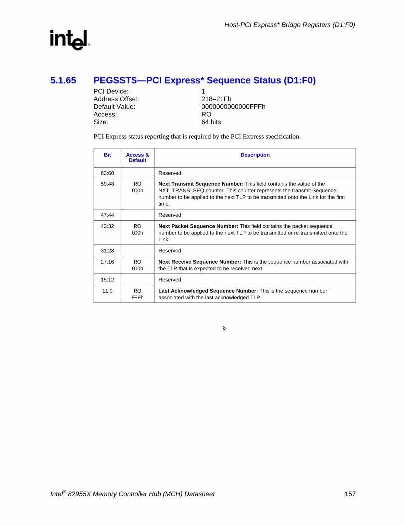
Host-PCI Express* Bridge Registers (D1:F0)
R
Intel® 82955X Memory Controller Hub (MCH) Datasheet 157
5.1.65 PEGSSTS—PCI Express* Sequence Status (D1:F0) PCI Device: 1 Address Offset: 218–21Fh Default Value: 0000000000000FFFh Access: RO Size: 64 bits
PCI Express status reporting that is required by the PCI Express specification.
Bit Access & Default
Description
63:60 Reserved
59:48 RO 000h
Next Transmit Sequence Number: This field contains the value of the NXT_TRANS_SEQ counter. This counter represents the transmit Sequence number to be applied to the next TLP to be transmitted onto the Link for the first time.
47:44 Reserved
43:32 RO 000h
Next Packet Sequence Number: This field contains the packet sequence number to be applied to the next TLP to be transmitted or re-transmitted onto the Link.
31:28 Reserved
27:16 RO 000h
Next Receive Sequence Number: This is the sequence number associated with the TLP that is expected to be received next.
15:12 Reserved
11:0 RO FFFh
Last Acknowledged Sequence Number: This is the sequence number associated with the last acknowledged TLP.
§
Host-PCI Express* Bridge Registers (D1:F0)
R
158 Intel® 82955X Memory Controller Hub (MCH) Datasheet
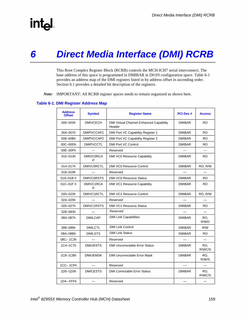
Direct Media Interface (DMI) RCRB
R
Intel® 82955X Memory Controller Hub (MCH) Datasheet 159
6 Direct Media Interface (DMI) RCRB This Root Complex Register Block (RCRB) controls the MCH-ICH7 serial interconnect. The base address of this space is programmed in DMIBAR in D0:F0 configuration space. Table 6-1 provides an address map of the DMI registers listed in by address offset in ascending order. Section 6.1 provides a detailed bit description of the registers.
Note: IMPORTANT: All RCRB register spaces needs to remain organized as shown here.
Table 6-1. DMI Register Address Map
Address Offset Symbol Register Name PCI Dev # Access
000–003h DMIVCECH DMI Virtual Channel Enhanced Capability Header
DMIBAR RO
004–007h DMIPVCCAP1 DMI Port VC Capability Register 1 DMIBAR RO
008–00Bh DMIPVCCAP2 DMI Port VC Capability Register 2 DMIBAR RO
00C–00Dh DMIPVCCTL DMI Port VC Control DMIBAR RO
00E–00Fh — Reserved — —
010–013h DMIVC0RCAP
DMI VC0 Resource Capability DMIBAR RO
014–017h DMIVC0RCTL DMI VC0 Resource Control DMIBAR RO, R/W
018–019h — Reserved — —
01A–01B h DMIVC0RSTS DMI VC0 Resource Status DMIBAR RO
01C–01F h DMIVC1RCAP
DMI VC1 Resource Capability DMIBAR RO
020–023h DMIVC1RCTL DMI VC1 Resource Control DMIBAR RO, R/W
024–025h — Reserved — —
026–027h DMIVC1RSTS DMI VC1 Resource Status DMIBAR RO
028–083h — Reserved — —
084–087h DMILCAP DMI Link Capabilities DMIBAR RO, R/WO
088–089h DMILCTL DMI Link Control DMIBAR R/W
08A–08Bh DMILSTS DMI Link Status DMIBAR RO
08C– 1C3h — Reserved — —
1C4–1C7h DMIUESTS DMI Uncorrectable Error Status DMIBAR RO, R/WC/S
1C8–1CBh DMIUEMSK DIM Uncorrectable Error Mask DMIBAR RO, R/W/S
1CC– 1CFh — Reserved — —
1D0–1D3h DMICESTS DMI Correctable Error Status DMIBAR RO, R/WC/S
1D4– FFFh — Reserved — —
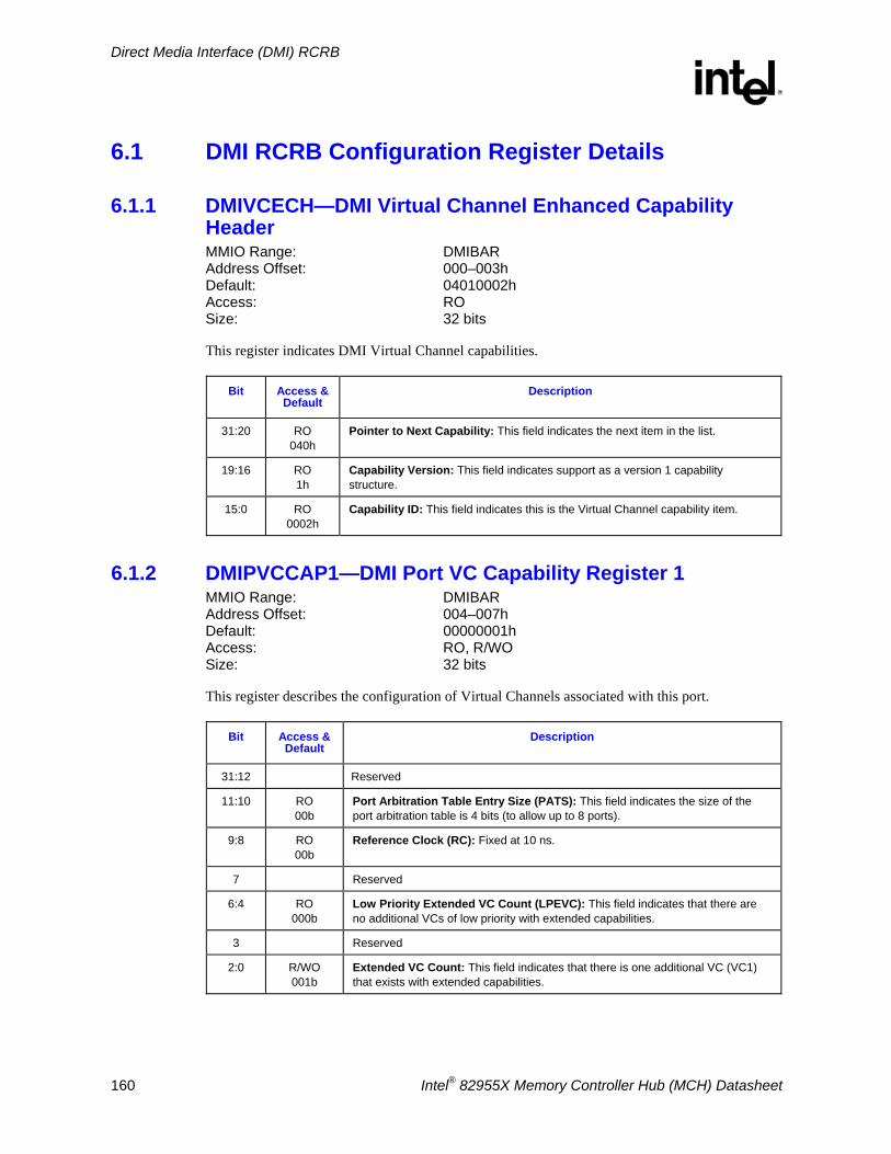
Direct Media Interface (DMI) RCRB
R
160 Intel® 82955X Memory Controller Hub (MCH) Datasheet
6.1 DMI RCRB Configuration Register Details
6.1.1 DMIVCECH—DMI Virtual Channel Enhanced Capability Header MMIO Range: DMIBAR Address Offset: 000–003h Default: 04010002h Access: RO Size: 32 bits
This register indicates DMI Virtual Channel capabilities.
Bit Access & Default
Description
31:20 RO 040h
Pointer to Next Capability: This field indicates the next item in the list.
19:16 RO 1h
Capability Version: This field indicates support as a version 1 capability structure.
15:0 RO 0002h
Capability ID: This field indicates this is the Virtual Channel capability item.
6.1.2 DMIPVCCAP1—DMI Port VC Capability Register 1 MMIO Range: DMIBAR Address Offset: 004–007h Default: 00000001h Access: RO, R/WO Size: 32 bits
This register describes the configuration of Virtual Channels associated with this port.
Bit Access & Default
Description
31:12 Reserved
11:10 RO 00b
Port Arbitration Table Entry Size (PATS): This field indicates the size of the port arbitration table is 4 bits (to allow up to 8 ports).
9:8 RO 00b
Reference Clock (RC): Fixed at 10 ns.
7 Reserved
6:4 RO 000b
Low Priority Extended VC Count (LPEVC): This field indicates that there are no additional VCs of low priority with extended capabilities.
3 Reserved
2:0 R/WO 001b
Extended VC Count: This field indicates that there is one additional VC (VC1) that exists with extended capabilities.
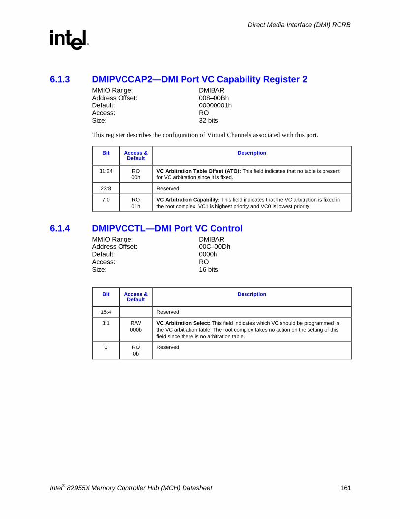
Direct Media Interface (DMI) RCRB
R
Intel® 82955X Memory Controller Hub (MCH) Datasheet 161
6.1.3 DMIPVCCAP2—DMI Port VC Capability Register 2 MMIO Range: DMIBAR Address Offset: 008–00Bh Default: 00000001h Access: RO Size: 32 bits
This register describes the configuration of Virtual Channels associated with this port.
Bit Access & Default
Description
31:24 RO 00h
VC Arbitration Table Offset (ATO): This field indicates that no table is present for VC arbitration since it is fixed.
23:8 Reserved
7:0 RO 01h
VC Arbitration Capability: This field indicates that the VC arbitration is fixed in the root complex. VC1 is highest priority and VC0 is lowest priority.
6.1.4 DMIPVCCTL—DMI Port VC Control MMIO Range: DMIBAR Address Offset: 00C–00Dh Default: 0000h Access: RO Size: 16 bits
Bit Access &
Default Description
15:4 Reserved
3:1 R/W 000b
VC Arbitration Select: This field indicates which VC should be programmed in the VC arbitration table. The root complex takes no action on the setting of this field since there is no arbitration table.
0 RO 0b
Reserved
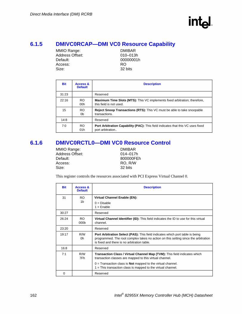
Direct Media Interface (DMI) RCRB
R
162 Intel® 82955X Memory Controller Hub (MCH) Datasheet
6.1.5 DMIVC0RCAP—DMI VC0 Resource Capability MMIO Range: DMIBAR Address Offset: 010–013h Default: 00000001h Access: RO Size: 32 bits
Bit Access &
Default Description
31:23 Reserved
22:16 RO 00h
Maximum Time Slots (MTS): This VC implements fixed arbitration; therefore, this field is not used.
15 RO 0b
Reject Snoop Transactions (RTS): This VC must be able to take snoopable transactions.
14:8 Reserved
7:0 RO 01h
Port Arbitration Capability (PAC): This field indicates that this VC uses fixed port arbitration..
6.1.6 DMIVC0RCTL0—DMI VC0 Resource Control MMIO Range: DMIBAR Address Offset: 014–017h Default: 800000FEh Access: RO, R/W Size: 32 bits
This register controls the resources associated with PCI Express Virtual Channel 0.
Bit Access & Default
Description
31 RO 1b
Virtual Channel Enable (EN): 0 = Disable 1 = Enable
30:27 Reserved
26:24 RO 000b
Virtual Channel Identifier (ID): This field indicates the ID to use for this virtual channel.
23:20 Reserved
19:17 R/W 0h
Port Arbitration Select (PAS): This field indicates which port table is being programmed. The root complex takes no action on this setting since the arbitration is fixed and there is no arbitration table.
16:8 Reserved
7:1 R/W 7Fh
Transaction Class / Virtual Channel Map (TVM): This field indicates which transaction classes are mapped to this virtual channel.
0 = Transaction class is Not mapped to the virtual channel. 1 = This transaction class is mapped to the virtual channel.
0 Reserved
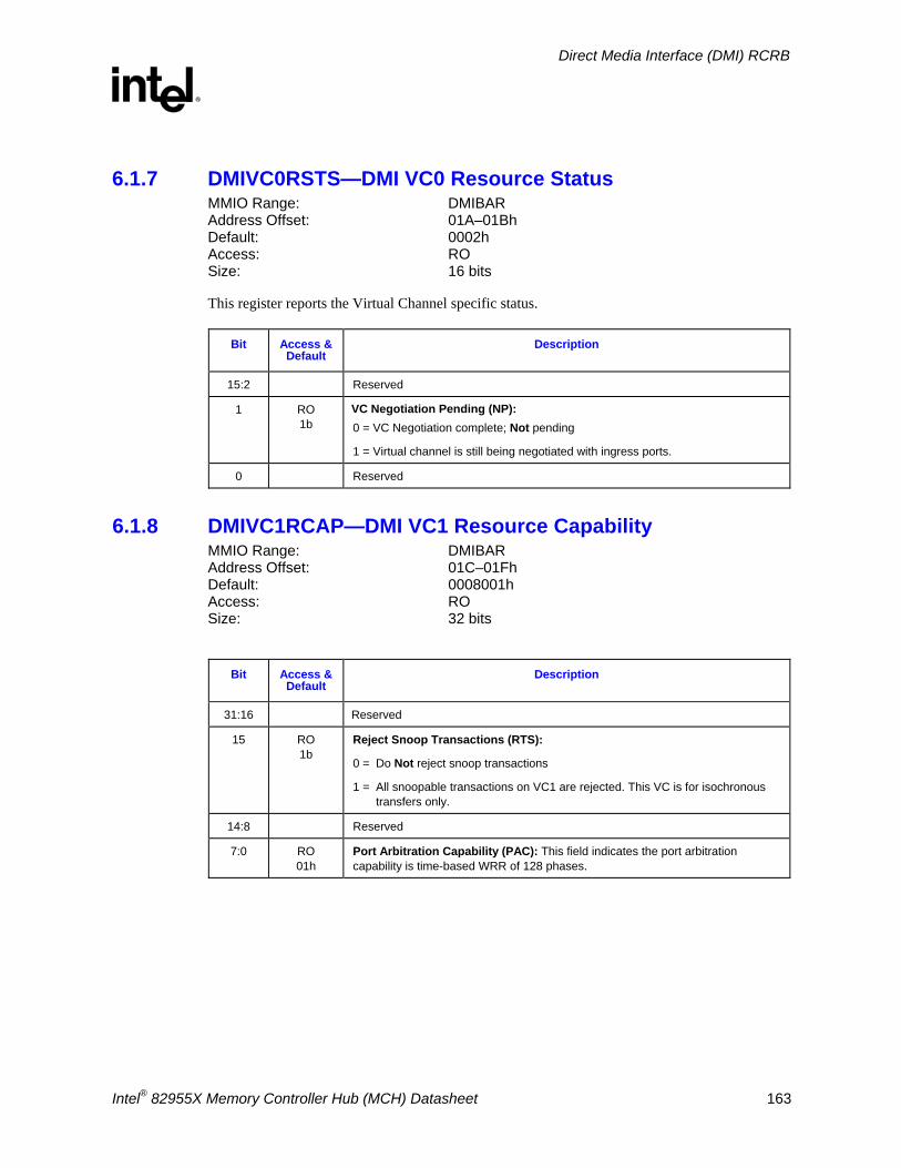
Direct Media Interface (DMI) RCRB
R
Intel® 82955X Memory Controller Hub (MCH) Datasheet 163
6.1.7 DMIVC0RSTS—DMI VC0 Resource Status MMIO Range: DMIBAR Address Offset: 01A–01Bh Default: 0002h Access: RO Size: 16 bits
This register reports the Virtual Channel specific status.
Bit Access & Default
Description
15:2 Reserved
1 RO 1b
VC Negotiation Pending (NP): 0 = VC Negotiation complete; Not pending
1 = Virtual channel is still being negotiated with ingress ports.
0 Reserved
6.1.8 DMIVC1RCAP—DMI VC1 Resource Capability MMIO Range: DMIBAR Address Offset: 01C–01Fh Default: 0008001h Access: RO Size: 32 bits
Bit Access &
Default Description
31:16 Reserved
15 RO 1b
Reject Snoop Transactions (RTS):
0 = Do Not reject snoop transactions
1 = All snoopable transactions on VC1 are rejected. This VC is for isochronous transfers only.
14:8 Reserved
7:0 RO 01h
Port Arbitration Capability (PAC): This field indicates the port arbitration capability is time-based WRR of 128 phases.
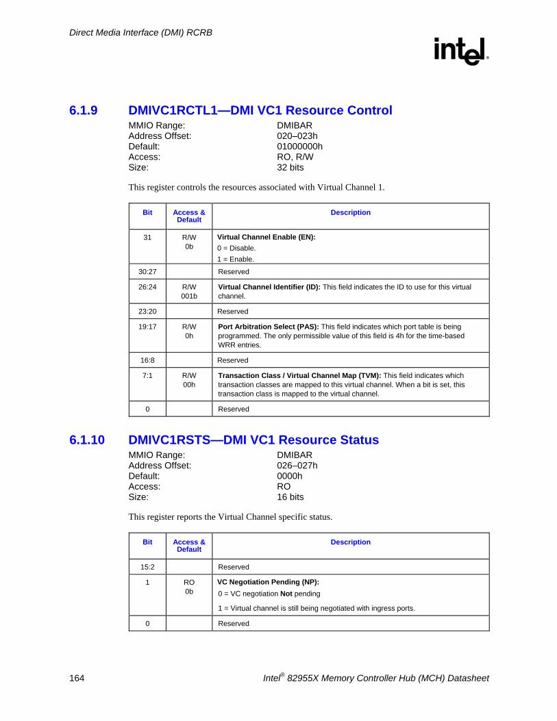
Direct Media Interface (DMI) RCRB
R
164 Intel® 82955X Memory Controller Hub (MCH) Datasheet
6.1.9 DMIVC1RCTL1—DMI VC1 Resource Control MMIO Range: DMIBAR Address Offset: 020–023h Default: 01000000h Access: RO, R/W Size: 32 bits
This register controls the resources associated with Virtual Channel 1.
Bit Access & Default
Description
31 R/W 0b
Virtual Channel Enable (EN): 0 = Disable. 1 = Enable.
30:27 Reserved
26:24 R/W 001b
Virtual Channel Identifier (ID): This field indicates the ID to use for this virtual channel.
23:20 Reserved
19:17 R/W 0h
Port Arbitration Select (PAS): This field indicates which port table is being programmed. The only permissible value of this field is 4h for the time-based WRR entries.
16:8 Reserved
7:1 R/W 00h
Transaction Class / Virtual Channel Map (TVM): This field indicates which transaction classes are mapped to this virtual channel. When a bit is set, this transaction class is mapped to the virtual channel.
0 Reserved
6.1.10 DMIVC1RSTS—DMI VC1 Resource Status MMIO Range: DMIBAR Address Offset: 026–027h Default: 0000h Access: RO Size: 16 bits
This register reports the Virtual Channel specific status.
Bit Access & Default
Description
15:2 Reserved
1 RO 0b
VC Negotiation Pending (NP): 0 = VC negotiation Not pending
1 = Virtual channel is still being negotiated with ingress ports.
0 Reserved
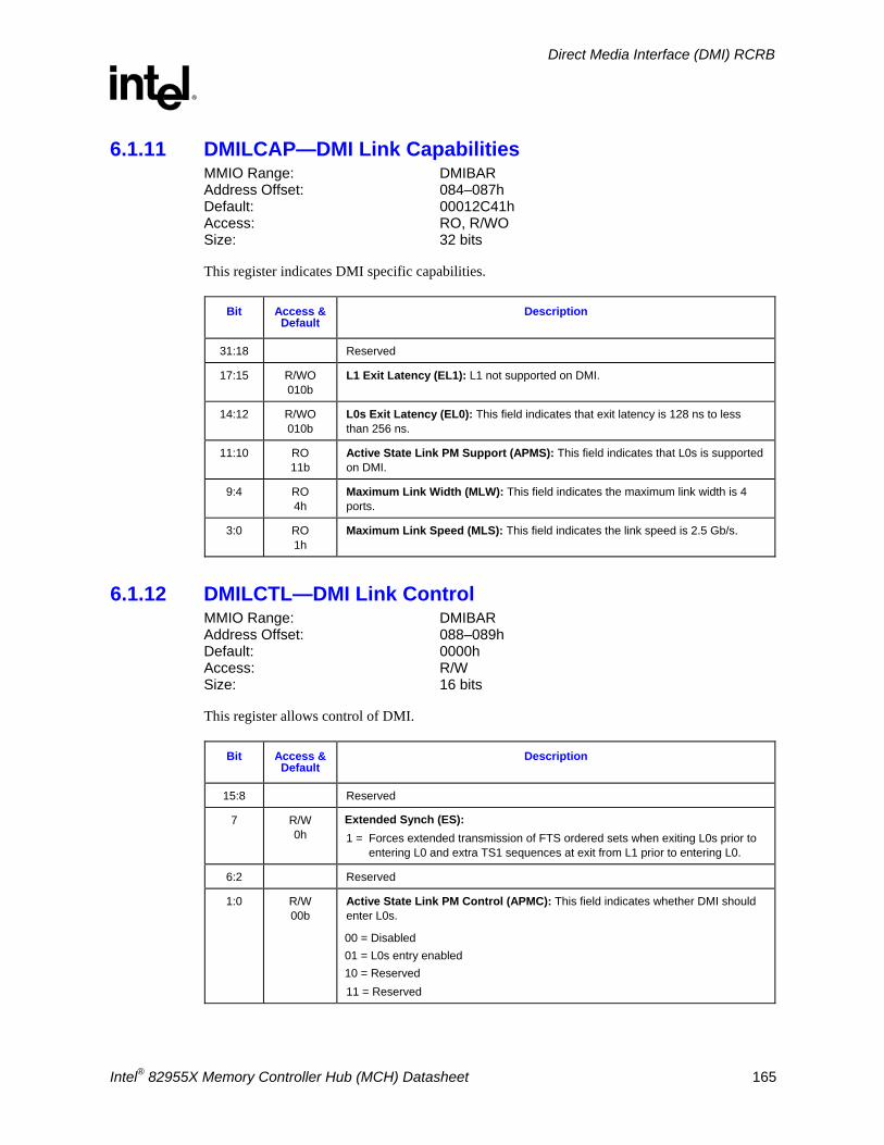
Direct Media Interface (DMI) RCRB
R
Intel® 82955X Memory Controller Hub (MCH) Datasheet 165
6.1.11 DMILCAP—DMI Link Capabilities MMIO Range: DMIBAR Address Offset: 084–087h Default: 00012C41h Access: RO, R/WO Size: 32 bits
This register indicates DMI specific capabilities.
Bit Access & Default
Description
31:18 Reserved
17:15 R/WO 010b
L1 Exit Latency (EL1): L1 not supported on DMI.
14:12 R/WO 010b
L0s Exit Latency (EL0): This field indicates that exit latency is 128 ns to less than 256 ns.
11:10 RO 11b
Active State Link PM Support (APMS): This field indicates that L0s is supported on DMI.
9:4 RO 4h
Maximum Link Width (MLW): This field indicates the maximum link width is 4 ports.
3:0 RO 1h
Maximum Link Speed (MLS): This field indicates the link speed is 2.5 Gb/s.
6.1.12 DMILCTL—DMI Link Control MMIO Range: DMIBAR Address Offset: 088–089h Default: 0000h Access: R/W Size: 16 bits
This register allows control of DMI.
Bit Access & Default
Description
15:8 Reserved
7 R/W 0h
Extended Synch (ES): 1 = Forces extended transmission of FTS ordered sets when exiting L0s prior to
entering L0 and extra TS1 sequences at exit from L1 prior to entering L0.
6:2 Reserved
1:0 R/W 00b
Active State Link PM Control (APMC): This field indicates whether DMI should enter L0s.
00 = Disabled 01 = L0s entry enabled 10 = Reserved 11 = Reserved
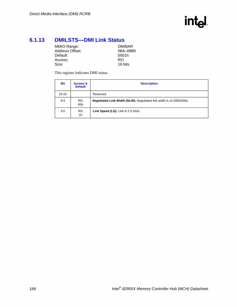
Direct Media Interface (DMI) RCRB
R
166 Intel® 82955X Memory Controller Hub (MCH) Datasheet
6.1.13 DMILSTS—DMI Link Status MMIO Range: DMIBAR Address Offset: 08A–08Bh Default: 0001h Access: RO Size: 16 bits
This register indicates DMI status.
Bit Access & Default
Description
15:10 Reserved
9:4 RO 00h
Negotiated Link Width (NLW): Negotiated link width is x4 (000100b).
3:0 RO 1h
Link Speed (LS): Link is 2.5 Gb/s.
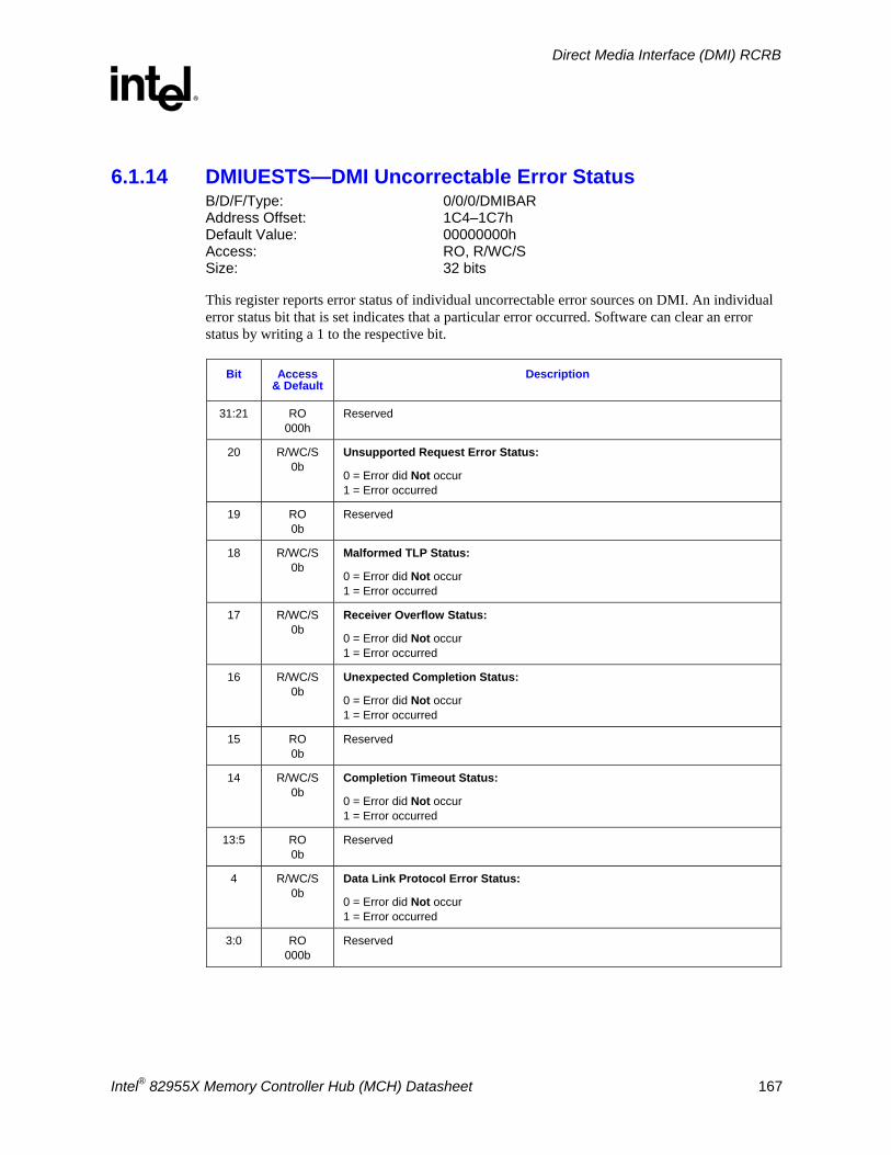
Direct Media Interface (DMI) RCRB
R
Intel® 82955X Memory Controller Hub (MCH) Datasheet 167
6.1.14 DMIUESTS—DMI Uncorrectable Error Status B/D/F/Type: 0/0/0/DMIBAR Address Offset: 1C4–1C7h Default Value: 00000000h Access: RO, R/WC/S Size: 32 bits
This register reports error status of individual uncorrectable error sources on DMI. An individual error status bit that is set indicates that a particular error occurred. Software can clear an error status by writing a 1 to the respective bit.
Bit Access & Default
Description
31:21 RO 000h
Reserved
20 R/WC/S 0b
Unsupported Request Error Status:
0 = Error did Not occur 1 = Error occurred
19 RO 0b
Reserved
18 R/WC/S 0b
Malformed TLP Status:
0 = Error did Not occur 1 = Error occurred
17 R/WC/S 0b
Receiver Overflow Status:
0 = Error did Not occur 1 = Error occurred
16 R/WC/S 0b
Unexpected Completion Status:
0 = Error did Not occur 1 = Error occurred
15 RO 0b
Reserved
14 R/WC/S 0b
Completion Timeout Status:
0 = Error did Not occur 1 = Error occurred
13:5 RO 0b
Reserved
4 R/WC/S 0b
Data Link Protocol Error Status:
0 = Error did Not occur 1 = Error occurred
3:0 RO 000b
Reserved
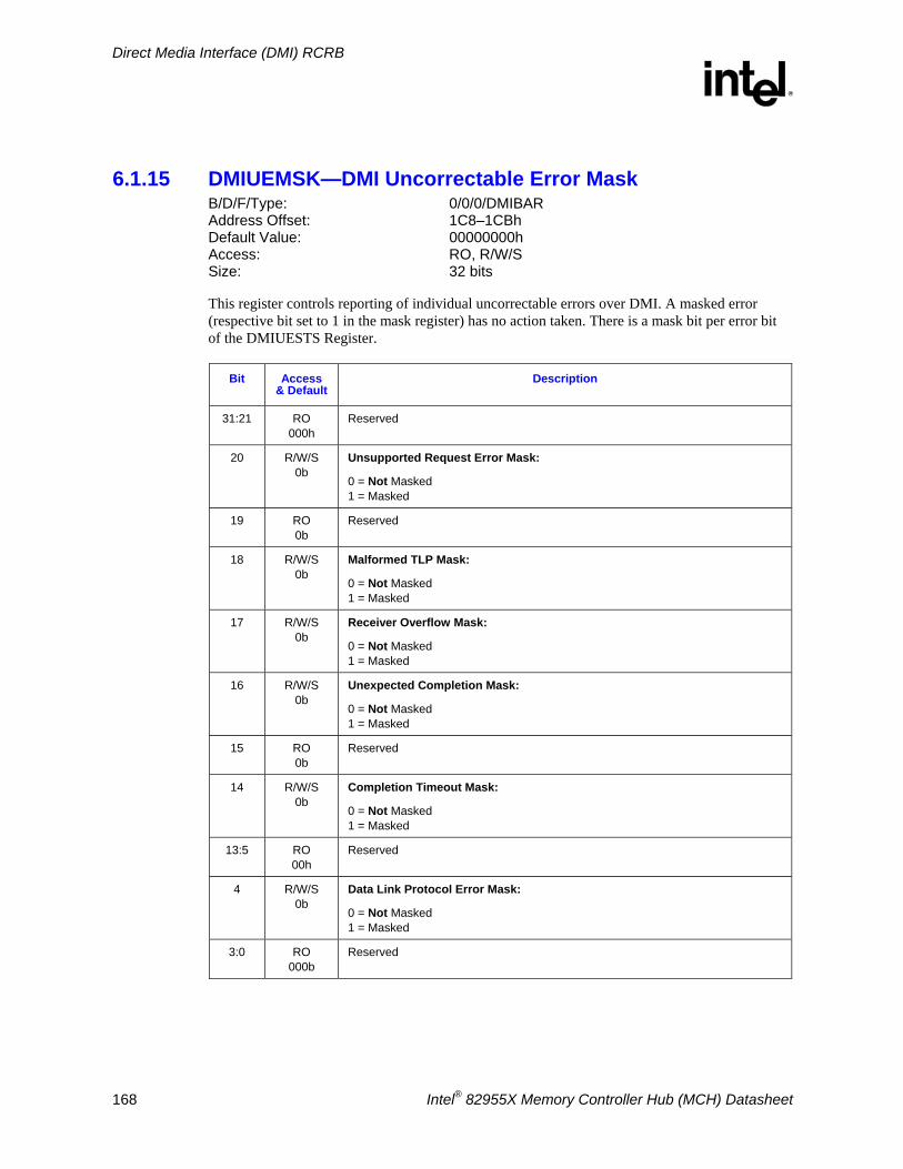
Direct Media Interface (DMI) RCRB
R
168 Intel® 82955X Memory Controller Hub (MCH) Datasheet
6.1.15 DMIUEMSK—DMI Uncorrectable Error Mask B/D/F/Type: 0/0/0/DMIBAR Address Offset: 1C8–1CBh Default Value: 00000000h Access: RO, R/W/S Size: 32 bits
This register controls reporting of individual uncorrectable errors over DMI. A masked error (respective bit set to 1 in the mask register) has no action taken. There is a mask bit per error bit of the DMIUESTS Register.
Bit Access & Default
Description
31:21 RO 000h
Reserved
20 R/W/S 0b
Unsupported Request Error Mask:
0 = Not Masked 1 = Masked
19 RO 0b
Reserved
18 R/W/S 0b
Malformed TLP Mask:
0 = Not Masked 1 = Masked
17 R/W/S 0b
Receiver Overflow Mask:
0 = Not Masked 1 = Masked
16 R/W/S 0b
Unexpected Completion Mask:
0 = Not Masked 1 = Masked
15 RO 0b
Reserved
14 R/W/S 0b
Completion Timeout Mask:
0 = Not Masked 1 = Masked
13:5 RO 00h
Reserved
4 R/W/S 0b
Data Link Protocol Error Mask:
0 = Not Masked 1 = Masked
3:0 RO 000b
Reserved
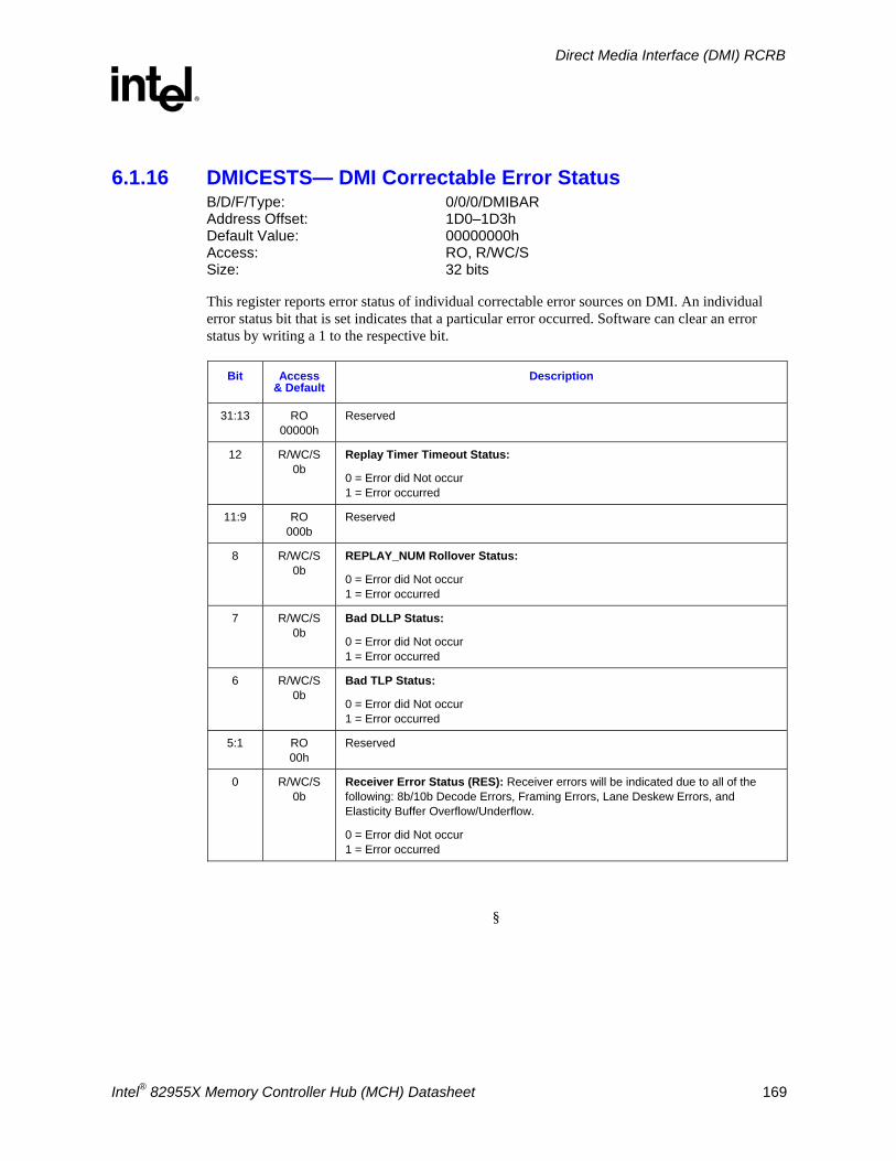
Direct Media Interface (DMI) RCRB
R
Intel® 82955X Memory Controller Hub (MCH) Datasheet 169
6.1.16 DMICESTS— DMI Correctable Error Status B/D/F/Type: 0/0/0/DMIBAR Address Offset: 1D0–1D3h Default Value: 00000000h Access: RO, R/WC/S Size: 32 bits
This register reports error status of individual correctable error sources on DMI. An individual error status bit that is set indicates that a particular error occurred. Software can clear an error status by writing a 1 to the respective bit.
Bit Access & Default
Description
31:13 RO 00000h
Reserved
12 R/WC/S 0b
Replay Timer Timeout Status:
0 = Error did Not occur 1 = Error occurred
11:9 RO 000b
Reserved
8 R/WC/S 0b
REPLAY_NUM Rollover Status:
0 = Error did Not occur 1 = Error occurred
7 R/WC/S 0b
Bad DLLP Status:
0 = Error did Not occur 1 = Error occurred
6 R/WC/S 0b
Bad TLP Status:
0 = Error did Not occur 1 = Error occurred
5:1 RO 00h
Reserved
0 R/WC/S 0b
Receiver Error Status (RES): Receiver errors will be indicated due to all of the following: 8b/10b Decode Errors, Framing Errors, Lane Deskew Errors, and Elasticity Buffer Overflow/Underflow.
0 = Error did Not occur 1 = Error occurred
§
Direct Media Interface (DMI) RCRB
R
170 Intel® 82955X Memory Controller Hub (MCH) Datasheet
System Address Map
R
Intel® 82955X Memory Controller Hub (MCH) Datasheet 171
7 System Address Map The MCH supports 64 GB of addressable memory space (see Figure 7-1) and 64 KB+3 bytes of addressable I/O space. A programmable memory address space under the 1-MB region is divided into regions that can be individually controlled with programmable attributes such as disable, read/write, write only, or read only. This section focuses on how the memory space is partitioned and what the separate memory regions are used for. I/O address space has simpler mapping and is explained near the end of this section.
Addressing of memory ranges larger than 4 GB is supported. The HREQ[4:3] FSB signals are decoded to determine whether the access is above or below 4 GB.
The MCH does support PCI Express port upper prefetchable base/limit registers. This allows the PCI Express to claim I/O accesses above 32 bit. Addressing of greater than 4 GB is allowed on both the DMI Interface and PCI Express interface. The MCH supports a maximum of 8 GB of DRAM; DRAM memory will Not be accessible above 12 GB. DRAM capacity is limited by the number of address signals available. There is no hardware lock to prevent the situation where more memory than is addressable is inserted.
In the following sections, it is assumed that all of the compatibility memory ranges reside on the DMI. The exception to this rule is VGA ranges that may be mapped to PCI Express or DMI. In the absence of more specific references, cycle descriptions referencing PCI should be interpreted as the DMI/PCI, while cycle descriptions referencing PCI Express are related to the PCI Express bus. The TOLUD Register is set to the appropriate value by BIOS. The remapbase/remaplimit registers remap logical accesses intended for addresses above 4 GB onto physical addresses that fall within DRAM.
The address map includes a number of programmable ranges:
• Device 0: ⎯ EPBAR – Egress port registers. Necessary for setting up VC1 as an isochronous channel
using time based weighted round robin arbitration. (4-KB window) ⎯ MCHBAR – Memory mapped range for internal MCH registers. For example, memory
buffer register controls. (16-KB window) ⎯ PCIEXBAR – Flat memory-mapped address space to access device configuration
registers. This mechanism can be used to access PCI configuration space (0–FFh) and Extended configuration space (100h–FFFh) for PCI Express devices. This enhanced configuration access mechanism is defined in the PCI Express specification. (64 MB, 128 MB, or 256-MB window)
⎯ DMIBAR – This window is used to access registers associated with the MCH/ ICH7 (DMI) register memory range. (4-KB window)
⎯ IFPBAR – Any write to this window will trigger a flush of the MCH’s Global Write Buffer to let software provide coherency between writes from an isochronous agent and writes from the processor (4-KB window).
• Device 1, Function 0: ⎯ MBASE1/MLIMIT1 – PCI Express port non-prefetchable memory access window. ⎯ PMBASE1/PMLIMIT1 – PCI Express port prefetchable memory access window. ⎯ IOBASE1/IOLIMIT1 – PCI Express port I/O access window.
The rules for the above programmable ranges are:
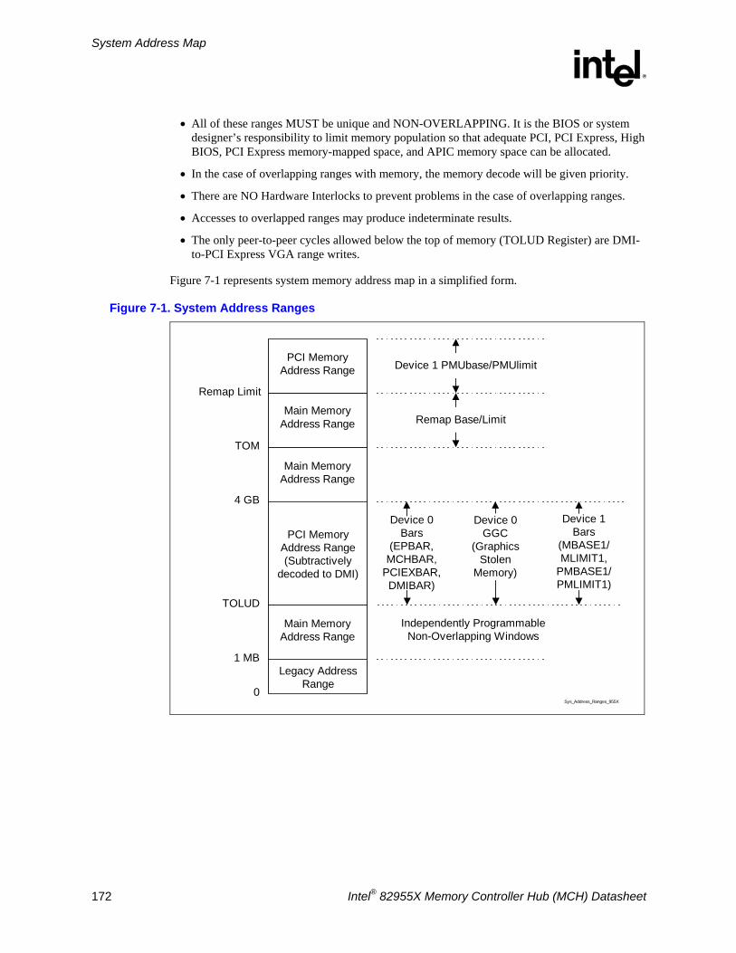
System Address Map
R
172 Intel® 82955X Memory Controller Hub (MCH) Datasheet
• All of these ranges MUST be unique and NON-OVERLAPPING. It is the BIOS or system designer’s responsibility to limit memory population so that adequate PCI, PCI Express, High BIOS, PCI Express memory-mapped space, and APIC memory space can be allocated.
• In the case of overlapping ranges with memory, the memory decode will be given priority.
• There are NO Hardware Interlocks to prevent problems in the case of overlapping ranges.
• Accesses to overlapped ranges may produce indeterminate results.
• The only peer-to-peer cycles allowed below the top of memory (TOLUD Register) are DMI-to-PCI Express VGA range writes.
Figure 7-1 represents system memory address map in a simplified form.
Figure 7-1. System Address Ranges
Main MemoryAddress Range
Legacy AddressRange
0
1 MB
TOLUD
4 GB
Independently ProgrammableNon-Overlapping Windows
Sys_Address_Ranges_955X
Main MemoryAddress Range
Main MemoryAddress Range
PCI MemoryAddress Range
TOM
Remap Limit
Device 1 PMUbase/PMUlimit
Remap Base/Limit
PCI MemoryAddress Range(Subtractively
decoded to DMI)
Device 0Bars
(EPBAR,MCHBAR,
PCIEXBAR,DMIBAR)
Device 0GGC
(GraphicsStolen
Memory)
Device 1Bars
(MBASE1/MLIMIT1,
PMBASE1/PMLIMIT1)
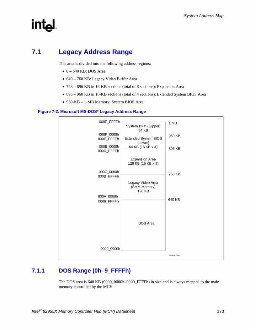
System Address Map
R
Intel® 82955X Memory Controller Hub (MCH) Datasheet 173
7.1 Legacy Address Range This area is divided into the following address regions:
• 0 – 640 KB: DOS Area
• 640 – 768 KB: Legacy Video Buffer Area
• 768 – 896 KB in 16-KB sections (total of 8 sections): Expansion Area
• 896 – 960 KB in 16-KB sections (total of 4 sections): Extended System BIOS Area
• 960-KB – 1-MB Memory: System BIOS Area
Figure 7-2. Microsoft MS-DOS* Legacy Address Range
000C_0000h
000D_FFFFh 896 KB000E_0000h
000E_FFFFh960 KB
000A_0000h
000B_FFFFh 768 KB
0000_0000h
0009_FFFFh 640 KB
000F_0000h
000F_FFFFh 1 MB
DOS Area
Legacy Video Area(SMM Memory)
128 KB
Expansion Area128 KB (16 KB x 8)
Extended System BIOS(Lower)
64 KB (16 KB x 4)
System BIOS (Upper)64 KB
MemMap_Legacy
7.1.1 DOS Range (0h–9_FFFFh)
The DOS area is 640 KB (0000_0000h–0009_FFFFh) in size and is always mapped to the main memory controlled by the MCH.
System Address Map
R
174 Intel® 82955X Memory Controller Hub (MCH) Datasheet
7.1.2 Legacy Video Area (A_0000h–B_FFFFh)
The legacy 128-KB VGA memory range, frame buffer, (000A_0000h–000B_FFFFh) can be mapped to PCI Express (Device 1), and/or to the DMI. The appropriate mapping depends on which devices are enabled and the programming of the VGA steering bits. Based on the VGA steering bits, priority for VGA mapping is constant. The MCH always decodes internally mapped devices first; internal to the MCH. The MCH always positively decodes internally mapped devices and PCI Express. Subsequent decoding of regions mapped to PCI Express or the DMI depends on the Legacy VGA configuration bits (VGA Enable and MDAP); see LAC Register (Device 0, offset 97h). This region is also the default for SMM space.
Compatible SMRAM Address Range (A_0000h–B_FFFFh)
When compatible SMM space is enabled, SMM-mode processor accesses to this range are routed to physical system DRAM at 000A_0000h–000B_FFFFh. Non-SMM-mode processor accesses to this range are considered to be to the Video Buffer Area as described above. PCI Express and DMI originated cycles to enabled SMM space are not allowed and are considered to be to the Video Buffer area. PCI Express and DMI initiated cycles are attempted as Peer cycles, and will master abort on PCI if no external VGA device claims them.
Monochrome Adapter (MDA) Range (B_0000h–B_7FFFh)
Legacy support requires the ability to have a second graphics controller (monochrome) in the system. Accesses in the standard VGA range are forwarded to PCI Express, or DMI (depending on configuration bits). Since the monochrome adapter may be mapped to any one of these devices, the MCH must decode cycles in the MDA range (000B_0000h–000B_7FFFh) and forward either to PCI Express, or the DMI. This capability is controlled by VGA steering bits and the legacy configuration bit (MDAP bit). In addition to the memory range B0000h to B7FFFh, the MCH decodes I/O cycles at 3B4h, 3B5h, 3B8h, 3B9h, 3Bah, and 3BFh and forwards them to the either PCI Express, and/or the DMI.
PCI Express* 16-bit VGA Decode
In the PCI to PCI Bridge Architecture Specification, Revision 1.2, it is required that 16-bit VGA decode be a feature. The VGA 16-bit decode originally was described in an ECR to the PCI to PCI Bridge Architecture Specification, Revision 1.1. This is now listed as a required feature in the updated Revision 1.2 specification.
7.1.3 Expansion Area (C_0000h–D_FFFFh)
This 128-KB ISA Expansion region (000C_0000h–000D_FFFFh) is divided into eight 16-KB segments (see Table 7-1). Each segment can be assigned one of four read/write states: read-only, write-only, read/write, or disabled. Typically, these blocks are mapped through the MCH and are subtractively decoded to ISA space. Memory that is disabled is not remapped.
Non-snooped accesses from PCI Express or DMI to this region are always sent to main memory.
System Address Map
R
Intel® 82955X Memory Controller Hub (MCH) Datasheet 175
Table 7-1. Expansion Area Memory Segments
Memory Segments Attributes Comments
0C0000h–0C3FFFh WE RE Add-on BIOS
0C4000h–0C7FFFh WE RE Add-on BIOS
0C8000h–0CBFFFh WE RE Add-on BIOS
0CC000h–0CFFFFh WE RE Add-on BIOS
0D0000h–0D3FFFh WE RE Add-on BIOS
0D4000h–0D7FFFh WE RE Add-on BIOS
0D8000h–0DBFFFh WE RE Add-on BIOS
0DC000h–0DFFFFh WE RE Add-on BIOS
7.1.4 Extended System BIOS Area (E_0000h–E_FFFFh)
This 64-KB area (000E_0000h–000E_FFFFh) is divided into four 16-KB segments (see Table 7-2). Each segment can be assigned independent read and write attributes so it can be mapped either to main memory or to DMI. Typically, this area is used for RAM or ROM. Memory segments that are disabled are not remapped elsewhere.
Non-snooped accesses from PCI Express or DMI to this region are always sent to main memory.
Table 7-2. Extended System BIOS Area Memory Segments
Memory Segments Attributes Comments
0E0000h–0E3FFFh WE RE BIOS Extension 0E4000h–0E7FFFh WE RE BIOS Extension 0E8000h–0EBFFFh WE RE BIOS Extension 0EC000h–0EFFFFh WE RE BIOS Extension
7.1.5 System BIOS Area (F_0000h–F_FFFFh)
This area is a single 64-KB segment (000F_0000h–000F_FFFFh). This segment can be assigned read and write attributes. It is by default (after reset) read/write disabled and cycles are forwarded to the DMI. By manipulating the read/write attributes, the MCH can “shadow” BIOS into main memory. When disabled, this segment is not remapped.
Non-snooped accesses from PCI Express or DMI to this region are always sent to DRAM.
Table 7-3. System BIOS Area Memory Segments
Memory Segments Attributes Comments
0F0000h–0FFFFFh WE RE BIOS Area
7.1.6 Programmable Attribute Map (PAM) Memory Area Details
The 13 sections from 768 KB to 1 MB comprise what is also known as the PAM memory area.
System Address Map
R
176 Intel® 82955X Memory Controller Hub (MCH) Datasheet
The MCH does not handle IWB (Implicit Write-Back) cycles targeting DMI. Since all memory residing on DMI should be set as non-cacheable, there will normally not be IWB cycles targeting DMI.
However, DMI becomes the default target for processor and DMI originated accesses to disabled segments of the PAM region. If the MTRRs covering the PAM regions are set to WB or RC it is possible to get IWB cycles targeting DMI. This may occur for DMI-originated cycles to disabled PAM regions.
For example, say that a particular PAM region is set for “Read Disabled” and the MTRR associated with this region is set to WB. A DMI master generates a memory read targeting the PAM region. A snoop is generated on the FSB and the result is an IWB. Since the PAM region is “Read Disabled”, the default target for the memory read becomes DMI. The IWB associated with this cycle will cause the MCH to hang.
7.2 Main Memory Address Range (1 MB to TOLUD) This address range (see Figure 7-3) extends from 1 MB to the top of physical memory that is permitted to be accessible by the MCH (as programmed in the TOLUD Register). All accesses to addresses within this range will be forwarded by the MCH to the main memory unless they fall into the optional TSEG or optional ISA Hole.
The MCH provides a maximum main memory address decode space of 8 GB. The MCH does not remap APIC or PCI Express memory space. This means that as the amount of physical memory populated in the system reaches 4 GB, there will be physical memory that exists yet is non-addressable and, therefore, unusable by the system. The MCH does not limit main memory address space in hardware.
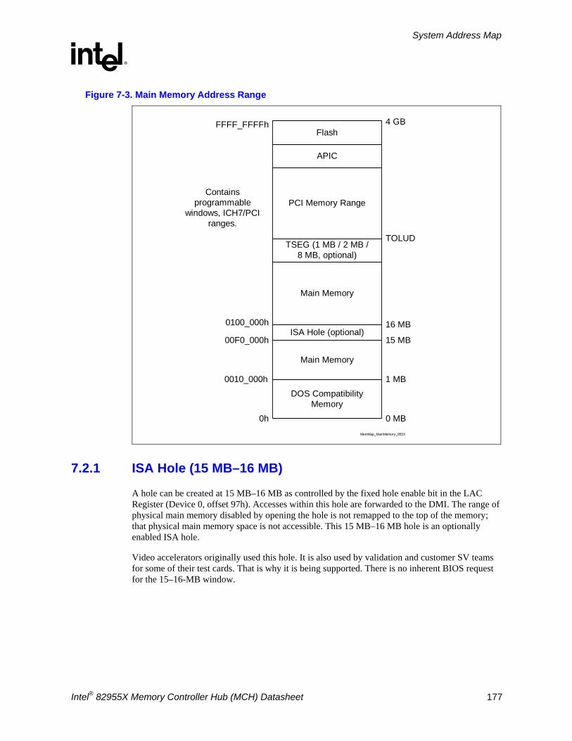
System Address Map
R
Intel® 82955X Memory Controller Hub (MCH) Datasheet 177
Figure 7-3. Main Memory Address Range
Flash
0h
Containsprogrammable
windows, ICH7/PCIranges.
TOLUD
MemMap_MainMemory_955X
APIC
PCI Memory Range
0010_000h
TSEG (1 MB / 2 MB /8 MB, optional)
Main Memory
ISA Hole (optional)
Main Memory
DOS CompatibilityMemory
00F0_000h
0100_000h
0 MB
1 MB
15 MB
16 MB
4 GBFFFF_FFFFh
7.2.1 ISA Hole (15 MB–16 MB)
A hole can be created at 15 MB–16 MB as controlled by the fixed hole enable bit in the LAC Register (Device 0, offset 97h). Accesses within this hole are forwarded to the DMI. The range of physical main memory disabled by opening the hole is not remapped to the top of the memory; that physical main memory space is not accessible. This 15 MB–16 MB hole is an optionally enabled ISA hole.
Video accelerators originally used this hole. It is also used by validation and customer SV teams for some of their test cards. That is why it is being supported. There is no inherent BIOS request for the 15–16-MB window.
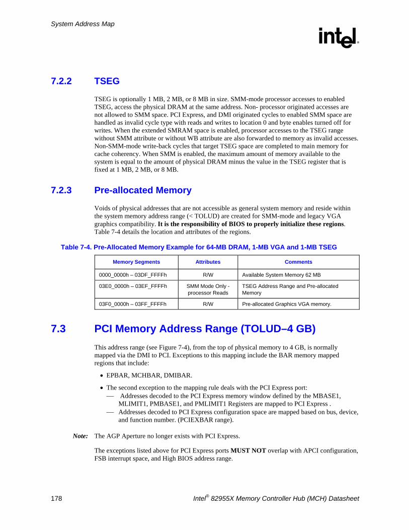
System Address Map
R
178 Intel® 82955X Memory Controller Hub (MCH) Datasheet
7.2.2 TSEG
TSEG is optionally 1 MB, 2 MB, or 8 MB in size. SMM-mode processor accesses to enabled TSEG, access the physical DRAM at the same address. Non- processor originated accesses are not allowed to SMM space. PCI Express, and DMI originated cycles to enabled SMM space are handled as invalid cycle type with reads and writes to location 0 and byte enables turned off for writes. When the extended SMRAM space is enabled, processor accesses to the TSEG range without SMM attribute or without WB attribute are also forwarded to memory as invalid accesses. Non-SMM-mode write-back cycles that target TSEG space are completed to main memory for cache coherency. When SMM is enabled, the maximum amount of memory available to the system is equal to the amount of physical DRAM minus the value in the TSEG register that is fixed at 1 MB, 2 MB, or 8 MB.
7.2.3 Pre-allocated Memory
Voids of physical addresses that are not accessible as general system memory and reside within the system memory address range (< TOLUD) are created for SMM-mode and legacy VGA graphics compatibility. It is the responsibility of BIOS to properly initialize these regions. Table 7-4 details the location and attributes of the regions.
Table 7-4. Pre-Allocated Memory Example for 64-MB DRAM, 1-MB VGA and 1-MB TSEG
Memory Segments Attributes Comments
0000_0000h – 03DF_FFFFh R/W Available System Memory 62 MB
03E0_0000h – 03EF_FFFFh SMM Mode Only - processor Reads
TSEG Address Range and Pre-allocated Memory
03F0_0000h – 03FF_FFFFh R/W Pre-allocated Graphics VGA memory.
7.3 PCI Memory Address Range (TOLUD–4 GB) This address range (see Figure 7-4), from the top of physical memory to 4 GB, is normally mapped via the DMI to PCI. Exceptions to this mapping include the BAR memory mapped regions that include:
• EPBAR, MCHBAR, DMIBAR.
• The second exception to the mapping rule deals with the PCI Express port: ⎯ Addresses decoded to the PCI Express memory window defined by the MBASE1,
MLIMIT1, PMBASE1, and PMLIMIT1 Registers are mapped to PCI Express . ⎯ Addresses decoded to PCI Express configuration space are mapped based on bus, device,
and function number. (PCIEXBAR range).
Note: The AGP Aperture no longer exists with PCI Express.
The exceptions listed above for PCI Express ports MUST NOT overlap with APCI configuration, FSB interrupt space, and High BIOS address range.
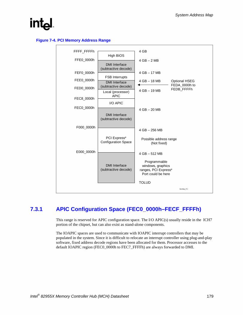
System Address Map
R
Intel® 82955X Memory Controller Hub (MCH) Datasheet 179
Figure 7-4. PCI Memory Address Range
High BIOS
E000_0000h
MemMap_PCI
DMI Interface(subtractive decode)
FSB InterruptsDMI Interface
(subtractive decode)Local (processor)
APIC
I/O APIC
DMI Interface(subtractive decode)
PCI Express*Configuration Space
DMI Interface(subtractive decode)
F000_0000h
FEC0_0000h
FEC8_0000h
FED0_0000h
FEE0_0000h
FEF0_0000h
FFE0_0000h
FFFF_FFFFh 4 GB
4 GB – 2 MB
4 GB – 17 MB
4 GB – 18 MB
4 GB – 19 MB
4 GB – 20 MB
4 GB – 256 MB
4 GB – 512 MB
TOLUD
Optional HSEGFEDA_0000h toFEDB_FFFFh
Possible address range(Not fixed)
Programmablewindows, graphics
ranges, PCI Express*Port could be here
7.3.1 APIC Configuration Space (FEC0_0000h–FECF_FFFFh)
This range is reserved for APIC configuration space. The I/O APIC(s) usually reside in the ICH7 portion of the chipset, but can also exist as stand-alone components.
The IOAPIC spaces are used to communicate with IOAPIC interrupt controllers that may be populated in the system. Since it is difficult to relocate an interrupt controller using plug-and-play software, fixed address decode regions have been allocated for them. Processor accesses to the default IOAPIC region (FEC0_0000h to FEC7_FFFFh) are always forwarded to DMI.
System Address Map
R
180 Intel® 82955X Memory Controller Hub (MCH) Datasheet
7.3.2 HSEG (FEDA_0000h–FEDB_FFFFh)
This optional segment from FEDA_0000h to FEDB_FFFFh provides a remapping window to SMM space. It is sometimes called the High SMM memory space. SMM-mode processor accesses to the optionally enabled HSEG are remapped to 000A_0000h–000B_FFFFh. Non-SMM-mode processor accesses to enabled HSEG are considered invalid and are terminated immediately on the FSB. The exceptions to this rule are Non-SMM-mode write-back cycles that are remapped to SMM space to maintain cache coherency. PCI Express and DMI originated cycles to enabled SMM space are not allowed. Physical main memory behind the HSEG transaction address is not remapped and is not accessible. All cacheline writes with WB attribute or implicit write-backs to the HSEG range are completed to main memory like a SMM cycle.
7.3.3 FSB Interrupt Memory Space (FEE0_0000–FEEF_FFFF)
The FSB Interrupt space is the address used to deliver interrupts to the FSB. Any device on PCI Express or DMI may issue a memory write to 0FEEx_xxxxh. The MCH forwards this memory write, along with the data, to the FSB as an Interrupt Message Transaction. The MCH terminates the FSB transaction by providing the response and asserting HTRDY#. This memory write cycle does not go to main memory.
7.3.4 High BIOS Area
The top 2 MB (FFE0_0000h–FFFF_FFFFh) of the PCI memory address range is reserved for system BIOS (High BIOS), extended BIOS for PCI devices, and the A20 alias of the system BIOS. The processor begins execution from the High BIOS after reset. This region is mapped to the DMI so that the upper subset of this region aliases to the 16-MB–256-KB range. The actual address space required for the BIOS is less than 2 MB, but the minimum processor MTRR range for this region is 2 MB so that full 2 MB must be considered.
7.4 Main Memory Address Space (4 GB to Remaplimit) The maximum main memory size supported is 8 GB total main memory. A hole between TOLUD and 4 GB occurs when main memory size approaches 4 GB or larger. As a result, a TOM Register and Remapbase/Remaplimit Registers become relevant.
The new remap configuration registers exist to reclaim lost main memory space.
Upstream write accesses above 36-bit addressing will be treated as peer writes by PCI Express and DMI. Upstream read accesses above 36-bit addressing will be treated as invalid cycles by PCI Express and DMI.
System Address Map
R
Intel® 82955X Memory Controller Hub (MCH) Datasheet 181
Top of Memory
This “Top of Memory” register reflects the total amount of populated physical memory. This is also the amount of addressable physical memory when remapping is used to ensure that no physical memory is wasted. This is NOT necessarily the highest main memory address (holes may exist in main memory address map due to addresses allocated for memory mapped I/O).
The TOLUD Register is restricted to 4 GB memory (A[31:27]), but the MCH can support up to 8 GB, limited by DRAM pins. For physical memory greater than 4 GB, the TOM Register helps identify the address range in-between the 4 GB boundary and the top of physical memory. This identifies memory that can be directly accessed (no remap address calculation) which is useful for memory access indication, early path indication, and trusted read indication.
C1DRB3 cannot be used directly to determine the effective size of memory as the values programmed in the DRBs depend on the memory mode (stacked, interleaved). The Remap Base/Limit registers also can not be used because remapping can be disabled. The TOM Register is used for early memory channel identification (channel 0 vs. channel 1) in the case of stacked memory.
7.4.1 Memory Re-claim Background
The following are examples of memory mapped I/O devices that are typically located below 4 GB:
• High BIOS • HSEG • TSEG • XAPIC • Local APIC • FSB Interrupts • PCI Express BAR • MCHBAR • EPBAR • DMIBAR • PMBASE/PMLIMIT, including PMBASEU/PMLIMITU • MBASE/MLIMIT
In previous generation MCHs, the physical main memory overlapped by the logical address space allocated to these memory mapped I/O devices was unusable. The result is that a large amount of physical memory populated in the system is unusable.
The MCH provides the capability to re-claim the physical memory overlapped by the memory mapped I/O logical address space. The MCH re-maps physical memory from the Top of Low Memory (TOLUD) boundary up to the 4 GB boundary to an equivalent sized logical address range located just above the top of physical memory.
7.4.2 Memory Re-mapping
An incoming address (referred to as a logical address) is checked to see if it falls in the memory re-map window. The bottom of the re-map window is defined by the value in the REMAPBASE
System Address Map
R
182 Intel® 82955X Memory Controller Hub (MCH) Datasheet
Register. The top of the re-map window is defined by the value in the REMAPLIMIT Register. An address that falls within this window is remapped to the physical memory starting at the address defined by the TOLUD Register.
7.4.3 PCI Express* Configuration Address Space
The PCIEXBAR Register (Device 0, offset 48h) defines the base address for the 256-MB block of addresses below the top of addressable memory (currently 4 GB) for the configuration space associated with all devices and functions that are potentially a part of the PCI Express root complex hierarchy. This range will be aligned to a 64 MB, 128 MB or 256-MB boundary. BIOS must assign this address range such that it will not conflict with any other address ranges.
7.4.4 PCI Express* Graphics Attach
The MCH can be programmed to direct memory accesses to the PCI Express interface when addresses are within either of two ranges specified via registers in MCH’s Device 1 configuration space.
• The first range is controlled via the Memory Base (MBASE) Register and Memory Limit (MLIMIT) Register.
• The second range is controlled via the Prefetchable Memory Base (PMBASE) Register and Prefetchable Memory Limit (PMLIMIT) Register.
The MCH positively decodes memory accesses to PCI Express memory address space as defined by the following inequalities:
Memory_Base_Address ≤ Address ≤ Memory_Limit_Address
Prefetchable_Memory_Base_Address ≤ Address ≤ Prefetchable_Memory_Limit_Address
It is essential to support a separate Prefetchable range to apply the USWC attribute (from the processor point of view) to that range. The USWC attribute is used by the processor for write combining.
Note that the MCH Device 1 memory range registers described above are used to allocate memory address space for any PCI Express devices on PCI Express that require such a window.
The PCICMD1 Register can override the routing of memory accesses to PCI Express. In other words, the memory access enable bit must be set in the device 1 PCICMD1 Register to enable the memory base/limit and prefetchable base/limit windows.
7.4.5 AGP DRAM Graphics Aperture
Unlike AGP4x, PCI Express has no concept of aperture for PCI Express devices. As a result, there is no need to translate addresses from PCI Express. Therefore, the MCH has no APBASE and APSIZE Registers.
System Address Map
R
Intel® 82955X Memory Controller Hub (MCH) Datasheet 183
7.5 System Management Mode (SMM) System Management Mode uses main memory for System Management RAM (SMM RAM). The MCH supports: Compatible SMRAM (C_SMRAM), High Segment (HSEG), and Top of Memory Segment (TSEG). System Management RAM space provides a memory area that is available for the SMI handlers and code and data storage. This memory resource is normally hidden from the system OS so that the processor has immediate access to this memory space upon entry to SMM. The MCH provides three SMRAM options:
• Below 1-MB option that supports compatible SMI handlers.
• Above 1-MB option that allows new SMI handlers to execute with write-back cacheable SMRAM.
• Optional TSEG area of 1 MB, 2 MB, or 8 MB in size.
• The above 1-MB solutions require changes to compatible SMRAM handlers’ code to properly execute above 1 MB.
Note: DMI and PCI Express masters are not allowed to access the SMM space.
7.5.1 SMM Space Definition
SMM space is defined by its addressed SMM space and its DRAM SMM space. The addressed SMM space is defined as the range of bus addresses used by the processor to access SMM space. DRAM SMM space is defined as the range of physical main memory locations containing the SMM code. SMM space can be accessed at one of three transaction address ranges: Compatible, High, and TSEG. The Compatible and TSEG SMM space is not remapped; therefore, the addressed and DRAM SMM space is the same address range. Since the High SMM space is remapped, the addressed and DRAM SMM space are different address ranges. Note that the High DRAM space is the same as the Compatible Transaction Address space. The following table describes three unique address ranges:
• Compatible Transaction Address
• High Transaction Address
• TSEG Transaction Address
SMM Space Enabled Transaction Address Space DRAM Space (DRAM)
Compatible (C) 000A_0000h to 000B_FFFFh 000A_0000h to 000B_FFFFh
High (H) FEDA_0000h to FEDB_FFFFh 000A_0000h to 000B_FFFFh
TSEG (T) (TOLUD –TSEG) to TOLUD (TOLUD–TSEG) to TOLUD
System Address Map
R
184 Intel® 82955X Memory Controller Hub (MCH) Datasheet
7.5.2 SMM Space Restrictions
If any of the following conditions are not met, the results of SMM accesses are unpredictable and may cause the system to hang: 1. The Compatible SMM space must not be set up as cacheable. 2. High or TSEG SMM transaction address space must not overlap address space assigned to
system main memory, or to any “PCI” devices (including DMI, PCI Express, and graphics devices). This is a BIOS responsibility.
3. Both D_OPEN and D_CLOSE must not be set to 1 at the same time. 4. When TSEG SMM space is enabled, the TSEG space must not be reported to the OS as
available main memory. This is a BIOS responsibility.
7.5.3 SMM Space Combinations
When High SMM is enabled (G_SMRAME=1 and H_SMRAM_EN=1), the compatible SMM space is effectively disabled. Processor-originated accesses to the compatible SMM space are forwarded to PCI Express if VGAEN=1 (also depends on MDAP); otherwise, they are forwarded to the DMI. PCI Express and DMI originated accesses are not allowed to access SMM space.
Table 7-5. SMM Space
Global Enable G_SMRAME
High Enable H_SMRAM_EN
TSEG Enable TSEG_EN
Compatible (C) Range
High (H) Range
TSEG (T) Range
0 X X Disable Disable Disable
1 0 0 Enable Disable Disable
1 0 1 Enable Disable Enable
1 1 0 Disabled Enable Disable
1 1 1 Disabled Enable Enable
7.5.4 SMM Control Combinations
The G_SMRAME bit provides a global enable for all SMM memory. The D_OPEN bit allows software to write to the SMM ranges without being in SMM mode. BIOS software can use this bit to initialize SMM code at powerup. The D_LCK bit limits the SMM range access to only SMM mode accesses. The D_CLS bit causes SMM data accesses to be forwarded to the DMI or PCI Express. The SMM software can use this bit to write to video memory while running SMM code out of main memory.
System Address Map
R
Intel® 82955X Memory Controller Hub (MCH) Datasheet 185
Table 7-6. SMM Control
G_SMRAME D_LCK D_CLS D_OPEN Processor in SMM Mode
SMM Code Access
SMM Data Access
0 x X x x Disable Disable
1 0 X 0 0 Disable Disable
1 0 0 0 1 Enable Enable
1 0 0 1 x Enable Enable
1 0 1 0 1 Enable Disable
1 0 1 1 x Invalid Invalid
1 1 X x 0 Disable Disable
1 1 0 x 1 Enable Enable
1 1 1 x 1 Enable Disable
7.5.5 SMM Space Decode and Transaction Handling
Only the processor is allowed to access SMM space. PCI Express and DMI originated transactions are not allowed to SMM space.
7.5.6 Processor WB Transaction to an Enabled SMM Address Space
Processor writeback transactions (HREQ[1]# = 0) to enabled SMM address space must be written to the associated SMM main memory even though D_OPEN=0 and the transaction is not performed in SMM mode. This ensures SMM space cache coherency when cacheable extended SMM space is used.
7.5.7 Memory Shadowing Any block of memory that can be designated as read-only or write-only can be “shadowed” into MCH main memory. Typically, this is done to allow ROM code to execute more rapidly out of main memory. ROM is used as read-only during the copy process while main memory at the same time is designated write-only. After copying, the main memory is designated read-only so that ROM is shadowed. Processor bus transactions are routed accordingly.
7.5.8 I/O Address Space
The MCH does not support the existence of any other I/O devices beside itself on the processor bus. The MCH generates either DMI or PCI Express bus cycles for all processor I/O accesses that it does not claim. Within the host bridge, the MCH contains two internal registers in the processor I/O space: Configuration Address (CONFIG_ADDRESS) Register and Configuration Data (CONFIG_DATA) Register. These locations are used to implement a configuration space access mechanism.
The processor allows 64 K+3 bytes to be addressed within the I/O space. The MCH propagates the processor I/O address without any translation on to the destination bus and, therefore,
System Address Map
R
186 Intel® 82955X Memory Controller Hub (MCH) Datasheet
provides addressability for 64 K+3 byte locations. Note that the upper 3 locations can be accessed only during I/O address wrap-around when the processor bus HA16# address signal is asserted. HA16# is asserted on the processor bus whenever an I/O access is made to 4 bytes from address 0FFFDh, 0FFFEh, or 0FFFFh. HA16# is also asserted when an I/O access is made to 2 bytes from address 0FFFFh.
The I/O accesses (other than ones used for configuration space access) are forwarded normally to the DMI bus unless they fall within the PCI Express I/O address range as defined by the mechanisms explained below. I/O writes are not posted. Memory writes to ICH7 or PCI Express are posted. The PCICMD1 Register can disable the routing of I/O cycles to PCI Express.
The MCH responds to I/O cycles initiated on PCI Express or DMI with a UR status. Upstream I/O cycles and configuration cycles should never occur. If one does occur, the request will route as a read to memory address 0h so a completion is naturally generated (whether the original request was a read or write). The transaction will complete with a UR completion status.
For Pentium processors, I/O reads that lie within 8-byte boundaries but cross 4-byte boundaries are issued from the processor as 1 transaction. The MCH breaks this into 2 separate transactions. I/O writes that lie within 8-byte boundaries but cross 4-byte boundaries are assumed to be split into 2 transactions by the processor.
7.5.9 PCI Express* I/O Address Mapping The MCH can be programmed to direct non-memory (I/O) accesses to the PCI Express bus interface when processor-initiated I/O cycle addresses are within the PCI Express I/O address range. This range is controlled via the I/O Base Address (IOBASE) and I/O Limit Address (IOLIMIT) Registers in MCH Device 1 configuration space.
7.5.10 MCH Decode Rules and Cross-Bridge Address Mapping
The following are MCH decode rules and cross-bridge address mapping used in this chipset:
• VGAA = 000A_0000 – 000A_FFFF • MDA = 000B_0000 – 000B_7FFF • VGAB = 000B_8000 – 000B_FFFF • MAINMEM = 0100_0000 to TOLUD
7.5.11 Legacy VGA and I/O Range Decode Rules The legacy 128-KB VGA memory range 000A_0000h–000B_FFFFh can be mapped to PCI Express (Device 1), and/or to the DMI depending on the programming of the VGA steering bits. Priority for VGA mapping is constant in that the MCH always decodes internally mapped devices first. The MCH always positively decodes internally mapped devices, namely PCI Express. Subsequent decoding of regions mapped to PCI Express or the DMI depends on the Legacy VGA configurations bits (VGA Enable and MDAP) in the LAC Register (Device 0).
§
Functional Description
R
Intel® 82955X Memory Controller Hub (MCH) Datasheet 187
8 Functional Description This chapter describes the MCH interfaces and major functional units.
8.1 Host Interface The MCH supports the Pentium 4 processor subset of the Enhanced Mode Scaleable Bus. The cache line size is 64 bytes. Source synchronous transfer is used for the address and data signals. The address signals are double pumped and a new address can be generated every other bus clock. At 200/267MHz bus clock the address signals run at 400/533MT/s. The data is quad pumped and an entire 64 Byte cache line can be transferred in two bus clocks. At 200/267MHz bus clock the data signals run at 800/1066MT/s for a maximum bandwidth of 10.7 GB/s.
8.1.1 FSB IOQ Depth
The Scalable Bus supports up to 12 simultaneous outstanding transactions.
8.1.2 FSB OOQ Depth
The MCH supports only one outstanding deferred transaction on the FSB.
8.1.3 FSB GTL+ Termination
The MCH integrates GTL+ termination resistors on die. Also, approximately 2.8pf (fast) – 3.3pf (slow) per pad of on die capacitance will be implemented to provide better FSB electrical performance.
8.1.4 FSB Dynamic Bus Inversion
The MCH supports Dynamic Bus Inversion (DBI) when driving and when receiving data from the processor. DBI limits the number of data signals that are driven to a low voltage on each quad pumped data phase. This decreases the worst-case power consumption of the MCH. HDINV[3:0]# indicate if the corresponding 16 bits of data are inverted on the bus for each quad pumped data phase:
HDINV[3:0]# Data Bits
HDINV0# HD[15:0]#
HDINV1# HD[31:16]#
HDINV2# HD[47:32]#
HDINV3# HD[63:48]#
Functional Description
R
188 Intel® 82955X Memory Controller Hub (MCH) Datasheet
When the processor or the MCH drives data, each 16-bit segment is analyzed. If more than 8 of the 16 signals would normally be driven low on the bus, the corresponding HDINV# signal will be asserted and the data will be inverted prior to being driven on the bus. When the processor or the MCH receives data, it monitors HDINV[3:0]# to determine if the corresponding data segment should be inverted.
8.1.4.1 APIC Cluster Mode Support
This is required for backwards compatibility with existing software, including various operating systems. As an example, beginning with Microsoft Windows 2000, there is a mode (boot.ini) that allows an end user to enable the use of cluster addressing support of the APIC.
The MCH supports three types of interrupt re-direction:
• Physical
• Flat-Logical
• Clustered-Logical
Functional Description
R
Intel® 82955X Memory Controller Hub (MCH) Datasheet 189
8.2 System Memory Controller The system memory controller supports two styles of memory organization (Interleaved and Asymmetric). Rules for populating DIMM slots are included in this section. Sample memory organizations are provided in Table 8-1 and Table 8-2.
Table 8-1. Sample System Memory Organization with Interleaved Channels
Channel A population
Cumulative Top Address in Channel A
Channel B Population
Cumulative Top Address in Channel B
Rank 3 0 MB 2560 MB 0 MB 2560 MB
Rank 2 256 MB 2560 MB 256 MB 2560 MB
Rank 1 512 MB 2048 MB 512 MB 2048 MB
Rank 0 512 MB 1024 MB 512 MB 1024 MB
Table 8-2. Sample System Memory Organization with Asymmetric Channels
Channel A population
Cumulative Top Address in Channel A
Channel B Population
Cumulative Top Address in Channel B
Rank 3 0 MB 1280 MB 0 MB 2560 MB
Rank 2 256 MB 1280 MB 256 MB 2560 MB
Rank 1 512 MB 1024 MB 512 MB 2304 MB
Rank 0 512 MB 512 MB 512 MB 1792 MB
Interleaved Mode
This mode provides maximum performance on real applications. Addresses are ping-ponged between the channels, and the switch happens after each cache line (64 byte boundary). If two consecutive cache lines are requested, both may be retrieved simultaneously, since they are on opposite channels. The drawbacks of Interleaved Mode are that the system designer must populate both channels of memory such that they have equal capacity; however, the technology and device width may vary from one channel to the other.
Enhanced Channel Interleaving
Transactions are issued to both channels simultaneously.
Asymmetric Mode
This mode trades performance for system design flexibility. Unlike the previous mode, addresses start in channel A and stay there until the end of the highest rank in channel A; then addresses continue from the bottom of channel B to the top. Real world applications are unlikely to make requests that alternate between addresses that sit on opposite channels with this memory organization. Thus, in most cases, bandwidth will be limited to that of a single channel. The system designer is free to populate or not to populate any rank on either channel, including either degenerate single channel case.
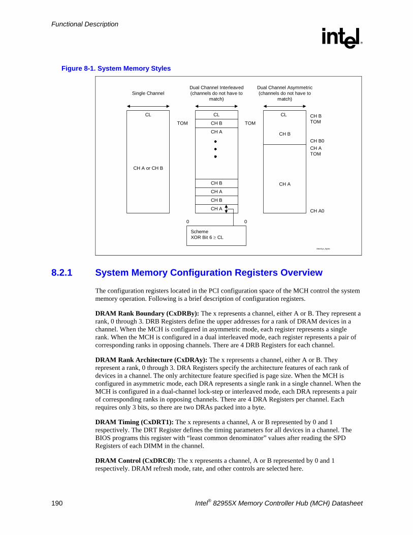
Functional Description
R
190 Intel® 82955X Memory Controller Hub (MCH) Datasheet
Figure 8-1. System Memory Styles
MemSys_Styles
Single Channel
CL CL CL
Dual Channel Interleaved(channels do not have to
match)
Dual Channel Asymmetric(channels do not have to
match)
CH B
CH A
CH B
CH A
CH B
CH A
0 0
SchemeXOR Bit 6 ≥ CL
CH A or CH B
CH B
CH A
TOM TOM
CH B0CH ATOM
CH A0
CH BTOM
8.2.1 System Memory Configuration Registers Overview
The configuration registers located in the PCI configuration space of the MCH control the system memory operation. Following is a brief description of configuration registers.
DRAM Rank Boundary (CxDRBy): The x represents a channel, either A or B. They represent a rank, 0 through 3. DRB Registers define the upper addresses for a rank of DRAM devices in a channel. When the MCH is configured in asymmetric mode, each register represents a single rank. When the MCH is configured in a dual interleaved mode, each register represents a pair of corresponding ranks in opposing channels. There are 4 DRB Registers for each channel.
DRAM Rank Architecture (CxDRAy): The x represents a channel, either A or B. They represent a rank, 0 through 3. DRA Registers specify the architecture features of each rank of devices in a channel. The only architecture feature specified is page size. When the MCH is configured in asymmetric mode, each DRA represents a single rank in a single channel. When the MCH is configured in a dual-channel lock-step or interleaved mode, each DRA represents a pair of corresponding ranks in opposing channels. There are 4 DRA Registers per channel. Each requires only 3 bits, so there are two DRAs packed into a byte.
DRAM Timing (CxDRT1): The x represents a channel, A or B represented by 0 and 1 respectively. The DRT Register defines the timing parameters for all devices in a channel. The BIOS programs this register with “least common denominator” values after reading the SPD Registers of each DIMM in the channel.
DRAM Control (CxDRC0): The x represents a channel, A or B represented by 0 and 1 respectively. DRAM refresh mode, rate, and other controls are selected here.
Functional Description
R
Intel® 82955X Memory Controller Hub (MCH) Datasheet 191
8.2.2 DRAM Technologies and Organization
"Single sided" below is a logical term referring to the number of chip selects attached to the DIMM. A real DIMM may put the components on both sides of the substrate, but be logically indistinguishable from single-sided DIMM, if all components on the DIMM are attached to the same chip select signal.
• x8 means that each component has 8 data lines.
• x16 means that each component has 16 data lines
All standard 256-Mb, 512-Mb, and 1-Gb technologies and addressing are supported for x16 and x8devices.
For DDR2 533 (PC 4300) ECC Version A = Single sided x8 Version B = Double sided x8 667 (PC 5300) ECC Version F = Single sided x8 Version G = Double sided x8
There is No support for DIMMs with different technologies or capacities on opposite sides of the same DIMM. If one side of a DIMM is populated, the other side is either identical or empty.
The DRAM sub-system supports single or dual channels, 64b or72b wide per channel. There can be a maximum of 4 ranks populated (2 Double Sided DIMMs) per channel. Mixed mode DDR DS-DIMMs (x8 and x16 on the same DIMM) are not supported.
By using 1Gb technology, the largest memory capacity is: 8 GB (16K rows * 1K columns * 1 cell/(row * column) * 8 b/cell * 8 banks/device * 8 devices/rank * 4 ranks/channel * 2 channel *1M/(K*K) * 1G/1024M * 1B/8b = 8 GB). Using 8 GB of memory is only possible in Interleaved mode with all ranks populated at maximum capacity. By using 256 Mb technology, the smallest memory capacity is: 128 MB (8K rows * 512 columns * 1 cell/(row * column) * 16b/cell * 4 banks/device * 4 devices/rank * 1 rank * 1M/1024K * 1B/8b = 128 MB).
8.2.2.1 Rules for Populating DIMM Slots • In all modes, the frequency of system memory will be the lowest frequency of all DIMMs in
the system, as determined through the SPD Registers on the DIMMs.
• In the Single Channel mode, any DIMM slot within the channel may be populated in any order. Either channel may be used. To save power, do not populate the unused channel.
• In Dual Channel Asymmetric mode, any DIMM slot may be populated in any order.
• In Dual Channel Interleaved mode, any DIMM slot may be populated in any order, but the total memory in each channel must be the same.
8.2.2.2 System Memory Supported Configurations
The MCH supports 256Mbit, 512Mbit, and 1Gbit technology based DIMMs from Table 8-3.
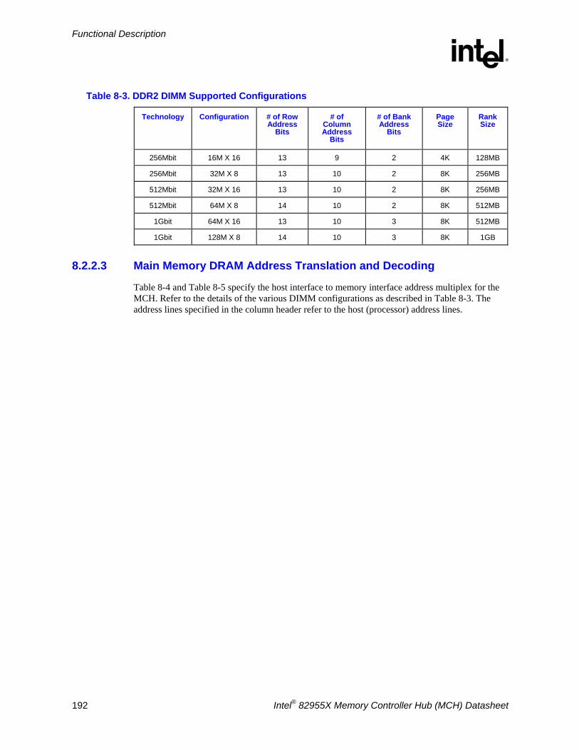
Functional Description
R
192 Intel® 82955X Memory Controller Hub (MCH) Datasheet
Table 8-3. DDR2 DIMM Supported Configurations
Technology Configuration # of Row Address
Bits
# of Column Address
Bits
# of Bank Address
Bits
Page Size
Rank Size
256Mbit 16M X 16 13 9 2 4K 128MB
256Mbit 32M X 8 13 10 2 8K 256MB
512Mbit 32M X 16 13 10 2 8K 256MB
512Mbit 64M X 8 14 10 2 8K 512MB
1Gbit 64M X 16 13 10 3 8K 512MB
1Gbit 128M X 8 14 10 3 8K 1GB
8.2.2.3 Main Memory DRAM Address Translation and Decoding
Table 8-4 and Table 8-5 specify the host interface to memory interface address multiplex for the MCH. Refer to the details of the various DIMM configurations as described in Table 8-3. The address lines specified in the column header refer to the host (processor) address lines.
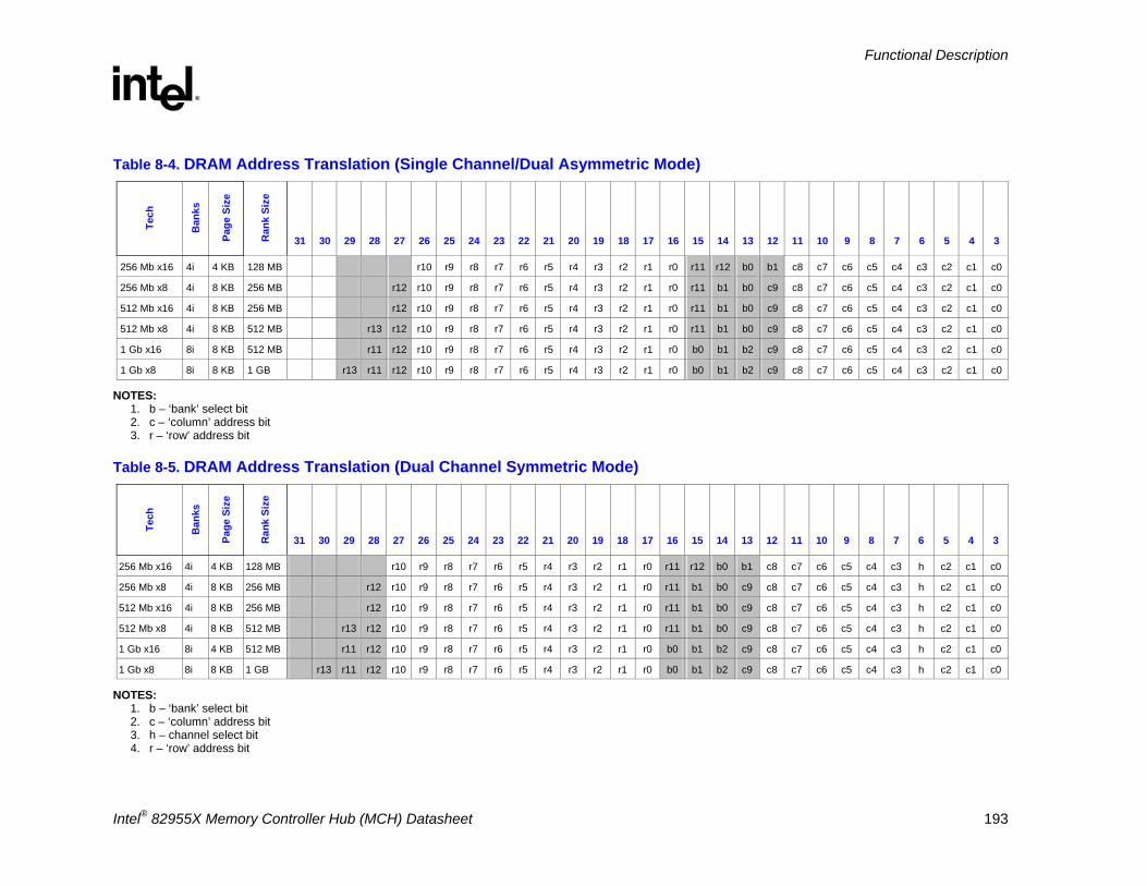
Functional Description
R
Intel® 82955X Memory Controller Hub (MCH) Datasheet 193
Table 8-4. DRAM Address Translation (Single Channel/Dual Asymmetric Mode) Te
ch
Ban
ks
Page
Siz
e
Ran
k Si
ze
31 30 29 28 27 26 25 24 23 22 21 20 19 18 17 16 15 14 13 12 11 10 9 8 7 6 5 4 3
256 Mb x16 4i 4 KB 128 MB r10 r9 r8 r7 r6 r5 r4 r3 r2 r1 r0 r11 r12 b0 b1 c8 c7 c6 c5 c4 c3 c2 c1 c0
256 Mb x8 4i 8 KB 256 MB r12 r10 r9 r8 r7 r6 r5 r4 r3 r2 r1 r0 r11 b1 b0 c9 c8 c7 c6 c5 c4 c3 c2 c1 c0
512 Mb x16 4i 8 KB 256 MB r12 r10 r9 r8 r7 r6 r5 r4 r3 r2 r1 r0 r11 b1 b0 c9 c8 c7 c6 c5 c4 c3 c2 c1 c0
512 Mb x8 4i 8 KB 512 MB r13 r12 r10 r9 r8 r7 r6 r5 r4 r3 r2 r1 r0 r11 b1 b0 c9 c8 c7 c6 c5 c4 c3 c2 c1 c0
1 Gb x16 8i 8 KB 512 MB r11 r12 r10 r9 r8 r7 r6 r5 r4 r3 r2 r1 r0 b0 b1 b2 c9 c8 c7 c6 c5 c4 c3 c2 c1 c0
1 Gb x8 8i 8 KB 1 GB r13 r11 r12 r10 r9 r8 r7 r6 r5 r4 r3 r2 r1 r0 b0 b1 b2 c9 c8 c7 c6 c5 c4 c3 c2 c1 c0
NOTES: 1. b – ‘bank’ select bit 2. c – ‘column’ address bit 3. r – ‘row’ address bit
Table 8-5. DRAM Address Translation (Dual Channel Symmetric Mode)
Tech
Ban
ks
Page
Siz
e
Ran
k Si
ze
31 30 29 28 27 26 25 24 23 22 21 20 19 18 17 16 15 14 13 12 11 10 9 8 7 6 5 4 3
256 Mb x16 4i 4 KB 128 MB r10 r9 r8 r7 r6 r5 r4 r3 r2 r1 r0 r11 r12 b0 b1 c8 c7 c6 c5 c4 c3 h c2 c1 c0
256 Mb x8 4i 8 KB 256 MB r12 r10 r9 r8 r7 r6 r5 r4 r3 r2 r1 r0 r11 b1 b0 c9 c8 c7 c6 c5 c4 c3 h c2 c1 c0
512 Mb x16 4i 8 KB 256 MB r12 r10 r9 r8 r7 r6 r5 r4 r3 r2 r1 r0 r11 b1 b0 c9 c8 c7 c6 c5 c4 c3 h c2 c1 c0
512 Mb x8 4i 8 KB 512 MB r13 r12 r10 r9 r8 r7 r6 r5 r4 r3 r2 r1 r0 r11 b1 b0 c9 c8 c7 c6 c5 c4 c3 h c2 c1 c0
1 Gb x16 8i 4 KB 512 MB r11 r12 r10 r9 r8 r7 r6 r5 r4 r3 r2 r1 r0 b0 b1 b2 c9 c8 c7 c6 c5 c4 c3 h c2 c1 c0
1 Gb x8 8i 8 KB 1 GB r13 r11 r12 r10 r9 r8 r7 r6 r5 r4 r3 r2 r1 r0 b0 b1 b2 c9 c8 c7 c6 c5 c4 c3 h c2 c1 c0
NOTES: 1. b – ‘bank’ select bit 2. c – ‘column’ address bit 3. h – channel select bit 4. r – ‘row’ address bit
Functional Description
R
194 Intel® 82955X Memory Controller Hub (MCH) Datasheet
8.2.2.4 ECC Support
The MCH supports ECC (Error Checking and Correction) and uses an ECC algorithm to protect against soft errors, when enabled. The algorithm works on a QWord (64-bit) basis. It corrects any single-bit error and detects any two-bits of error. An odd number of errors greater than 1, will either be detected correctly or will be misinterpreted as a single-bit error, and cannot be corrected. An error in an even number of bits greater than two will either be detected as a multi-bit error or it may not be detected at all.
8.2.3 DRAM Clock Generation The MCH generates three differential clock pairs for every supported DIMM. There are total of 6 clock pairs driven directly by the MCH to 2 DIMMs per channel.
8.2.4 Suspend To RAM and Resume
When entering the Suspend to RAM (STR) state, the SDRAM controller will flush pending cycles and then enter all SDRAM rows into self refresh. In STR, the CKE signals remain low so the SDRAM devices will perform self-refresh.
8.2.5 DDR2 On Die Termination
On die termination (ODT) is a feature that allows a DRAM to turn on/off internal termination resistance for each DQ, DM, DQS, and DQS# signal for x8 and x16 configurations via the ODT control signals. The ODT feature is designed to improve signal integrity of the memory channel by allowing the termination resistance for the DQ, DM, DQS, and DQS# signals to be located inside the DRAM devices themselves instead of on the motherboard. The MCH drives out the required ODT signals, based on memory configuration and which rank is being written to or read from, to the DRAM devices on a targeted DIMM rank to enable or disable their termination resistance.
Functional Description
R
Intel® 82955X Memory Controller Hub (MCH) Datasheet 195
8.3 PCI Express* See Chapter 1 for a list of PCI Express features and the PCI Express specification for further details.
This MCH is part of a PCI Express root complex. This means it connects a host processor / memory subsystem to a PCI Express hierarchy. The control registers for this functionality are located in device 1 configuration space and two Root Complex Register Blocks (RCRBs). The DMI RCRB contains registers for control of the ICH7 attach ports.
8.3.1 PCI Express* Architecture
The PCI Express architecture is specified in layers. Compatibility with the PCI addressing model (a load-store architecture with a flat address space) is maintained to ensure that all existing applications and drivers operate unchanged. The PCI Express configuration uses standard mechanisms as defined in the PCI Plug-and-Play specification. The initial speed of 1.25 GHz (250 MHz internally) results in 2.5 Gb/s/direction that provides a 250 MB/s communications channel in each direction (500 MB/s total); this is close to twice the data rate of classic PCI per lane.
8.3.1.1 Transaction Layer
The upper layer of the PCI Express architecture is the Transaction Layer. The Transaction Layer’s primary responsibility is the assembly and disassembly of Transaction Layer Packets (TLPs). TLPs are used to communicate transactions (such as, read and write) as well as certain types of events. The Transaction Layer also manages flow control of TLPs.
8.3.1.2 Data Link Layer
The middle layer in the PCI Express stack, the Data Link Layer, serves as an intermediate stage between the Transaction Layer and the Physical Layer. Responsibilities of Data Link Layer include link management, error detection, and error correction.
8.3.1.3 Physical Layer
The Physical Layer includes all circuitry for interface operation, including driver and input buffers, parallel-to-serial and serial-to-parallel conversion, PLL(s), and impedance matching circuitry.
Functional Description
R
196 Intel® 82955X Memory Controller Hub (MCH) Datasheet
8.4 Power Management Power management feature include:
• ACPI 1.0b support
• ACPI S0, S1D, S3 (both Cold and Chipset Hot), S4, S5, C0, and C1. The C2, C3, C4 states and corresponding Enhanced states- S3hot, C2, C3, and C4 are not used in the MCH.
• Enhanced power management state transitions for increasing time that the processor spends in low power states
• Graphics Adapter States: D0, D3.
• PCI Express Link States: L0, L0s, L1, L2/L3 Ready, L3
8.5 Clocking The MCH has PLLs that provide the internal clocks. The PLLs are:
• Host PLL – Generates the main core clocks in the host clock domain. This PLL can also be used to generate memory core clocks. It uses the Host clock (HCLKIN) as a reference.
• Memory PLL – Can be used to generate memory core clocks, when not generated by the Host PLL. This PLL is not needed in all configurations, but exists to provide more flexible frequency combinations without an unreasonable VCO frequency. It uses the Host clock (HCLKIN) as a reference.
• PCI Express PLL – Generates all PCI Express related clocks, including the Direct Media Interface that connects to the ICH7. This PLL uses the 100 MHz (GCLKIN) as a reference.
Figure 8-2 illustrates the various clocks in the platform.
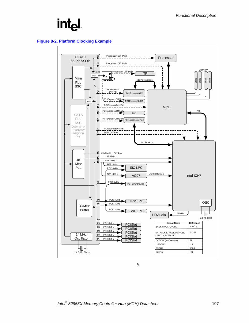
Functional Description
R
Intel® 82955X Memory Controller Hub (MCH) Datasheet 197
Figure 8-2. Platform Clocking Example
PCI Down Dev ice
CK41056-Pin SSOP
MainPLLSSC
SATAPLLSSC
Optional forfrequencymargining
only
48MHz PLL
33 MHzBuffer
14 MHzOscillator
HD Audio 24 MHz
Intel® ICH7
OSC
32.768kHz
FWH LPC
PCI ExpressDIf f Pair
SATA Dif f Pair
PCI SlotPCI Slot
PCI 33 MHz
SIO LPC
AC97 AC97 Bit Clock
TPM LPC
4 x1 PCI Exp
DMI
PCI Slot
PCI 33 MHz
PCI 33 MHz
PCI 33 MHz
PCI 33 MHz
PCI 33 MHz
PCI 33 MHz
REF 14 MHz
REF 14 MHz
REF 14 MHz
USB 48MHzDOT 96 MHz Dif f Pair
Memory
Slot
0
Slot
1
Slot
2
Slot
3
ITP
ProcessorProcessor Diff Pair
Processor Diff Pair
Processor Diff Pair
PCI Express GFX
x16 PCI Express
Mux PCI Express SLOT
PCI SlotPCI Slot
PCI 33 MHz
PCI 33 MHz
PCI 33 MHz
Mux
P1
P2
P3
P4
P5
P6
P7
P8
R1U1
D1
S1
S2
S3
S4
S5
S6
C3/S7
C2
C1
P9
LAN
PCI Express DIf f Pair
PCI Express DIf f Pair
PCI Express DIf f Pair
PCI Express DIf f Pair
PCI Express DIf f Pair
PCI Express Dev ice
BCLK, ITPCLK, HCLK
SATACLK, ICHCLK, MCHCLK,LANCLK, PCIECLK
DOTCLK (No Connect)
USBCLK
PCICLK
REFCLK
C1-C3
S1-S7
D1
U1
P1-9
R1
Signal Name Reference
MCH
14.31818MHz
§
Functional Description
R
198 Intel® 82955X Memory Controller Hub (MCH) Datasheet
Electrical Characteristics
R
Intel® 82955X Memory Controller Hub (MCH) Datasheet 199
9 Electrical Characteristics This chapter contains the MCH absolute maximum electrical ratings, power dissipation values, and DC characteristics.
9.1 Absolute Minimum and Maximum Ratings Table 9-1 specifies the 955X Express chipset MCH’s absolute maximum and minimum ratings. Within functional operation limits, functionality and long-term reliability can be expected.
At conditions outside functional operation condition limits, but within absolute maximum and minimum ratings, neither functionality nor long-term reliability can be expected. If a device is returned to conditions within functional operation limits after having been subjected to conditions outside these limits, but within the absolute maximum and minimum ratings, the device may be functional, but its lifetime may be degraded depending on exposure to conditions exceeding the functional operation condition limits.
At conditions exceeding absolute maximum and minimum ratings, neither functionality nor long-term reliability can be expected. Moreover, if a device is subjected to these conditions for any length of time then, when returned to conditions within the functional operating condition limits, it will either not function, or its reliability will be severely degraded.
Although the MCH contains protective circuitry to help resist damage from static electric discharge, additional precautions should always be taken to avoid damage from high static voltages or electric fields.
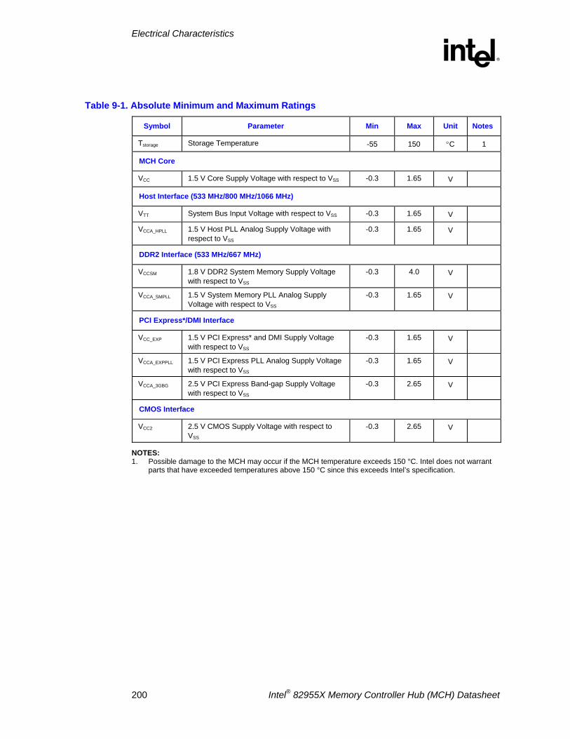
Electrical Characteristics
R
200 Intel® 82955X Memory Controller Hub (MCH) Datasheet
Table 9-1. Absolute Minimum and Maximum Ratings
Symbol Parameter Min Max Unit Notes
Tstorage Storage Temperature -55 150 °C 1
MCH Core
VCC 1.5 V Core Supply Voltage with respect to VSS -0.3 1.65 V
Host Interface (533 MHz/800 MHz/1066 MHz)
VTT System Bus Input Voltage with respect to VSS -0.3 1.65 V
VCCA_HPLL 1.5 V Host PLL Analog Supply Voltage with respect to VSS
-0.3 1.65 V
DDR2 Interface (533 MHz/667 MHz)
VCCSM 1.8 V DDR2 System Memory Supply Voltage with respect to VSS
-0.3 4.0 V
VCCA_SMPLL 1.5 V System Memory PLL Analog Supply Voltage with respect to VSS
-0.3 1.65 V
PCI Express*/DMI Interface
VCC_EXP 1.5 V PCI Express* and DMI Supply Voltage with respect to VSS
-0.3 1.65 V
VCCA_EXPPLL 1.5 V PCI Express PLL Analog Supply Voltage with respect to VSS
-0.3 1.65 V
VCCA_3GBG 2.5 V PCI Express Band-gap Supply Voltage with respect to VSS
-0.3 2.65 V
CMOS Interface
VCC2 2.5 V CMOS Supply Voltage with respect to VSS
-0.3 2.65 V
NOTES: 1. Possible damage to the MCH may occur if the MCH temperature exceeds 150 °C. Intel does not warrant
parts that have exceeded temperatures above 150 °C since this exceeds Intel’s specification.
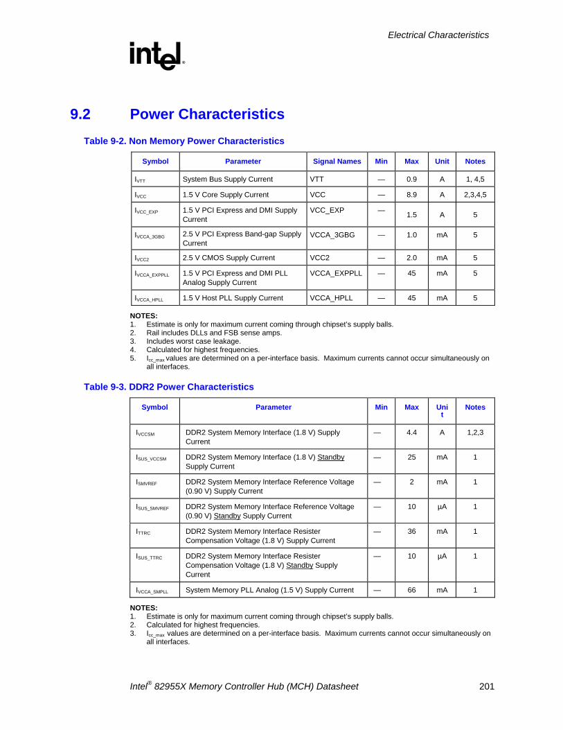
Electrical Characteristics
R
Intel® 82955X Memory Controller Hub (MCH) Datasheet 201
9.2 Power Characteristics Table 9-2. Non Memory Power Characteristics
Symbol Parameter Signal Names Min Max Unit Notes
IVTT System Bus Supply Current VTT — 0.9 A 1, 4,5
IVCC 1.5 V Core Supply Current VCC — 8.9 A 2,3,4,5
IVCC_EXP 1.5 V PCI Express and DMI Supply Current
VCC_EXP — 1.5 A 5
IVCCA_3GBG 2.5 V PCI Express Band-gap Supply Current
VCCA_3GBG — 1.0 mA 5
IVCC2 2.5 V CMOS Supply Current VCC2 — 2.0 mA 5
IVCCA_EXPPLL 1.5 V PCI Express and DMI PLL Analog Supply Current
VCCA_EXPPLL — 45 mA 5
IVCCA_HPLL 1.5 V Host PLL Supply Current VCCA_HPLL — 45 mA 5
NOTES: 1. Estimate is only for maximum current coming through chipset’s supply balls. 2. Rail includes DLLs and FSB sense amps. 3. Includes worst case leakage. 4. Calculated for highest frequencies. 5. Icc_max values are determined on a per-interface basis. Maximum currents cannot occur simultaneously on
all interfaces.
Table 9-3. DDR2 Power Characteristics
Symbol Parameter Min Max Unit
Notes
IVCCSM DDR2 System Memory Interface (1.8 V) Supply Current
— 4.4 A 1,2,3
ISUS_VCCSM DDR2 System Memory Interface (1.8 V) Standby Supply Current
— 25 mA 1
ISMVREF DDR2 System Memory Interface Reference Voltage (0.90 V) Supply Current
— 2 mA 1
ISUS_SMVREF DDR2 System Memory Interface Reference Voltage (0.90 V) Standby Supply Current
— 10 µA 1
ITTRC DDR2 System Memory Interface Resister Compensation Voltage (1.8 V) Supply Current
— 36 mA 1
ISUS_TTRC DDR2 System Memory Interface Resister Compensation Voltage (1.8 V) Standby Supply Current
— 10 µA 1
IVCCA_SMPLL System Memory PLL Analog (1.5 V) Supply Current — 66 mA 1
NOTES: 1. Estimate is only for maximum current coming through chipset’s supply balls. 2. Calculated for highest frequencies. 3. Icc_max values are determined on a per-interface basis. Maximum currents cannot occur simultaneously on
all interfaces.
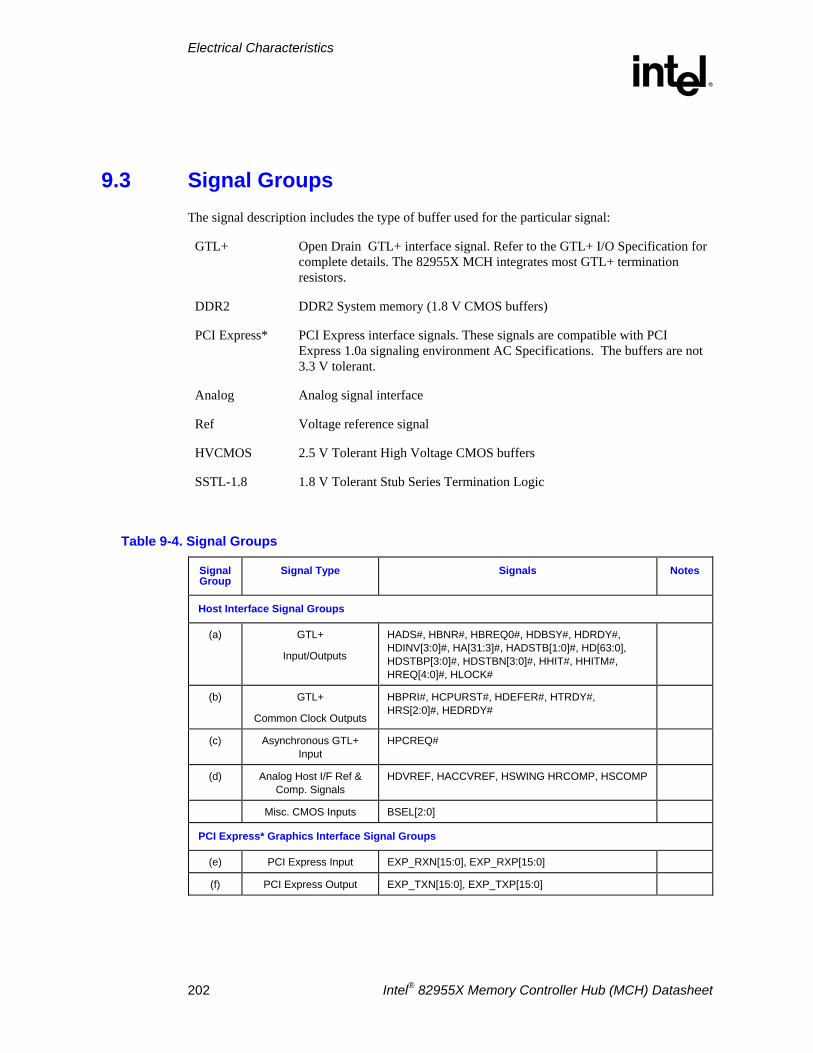
Electrical Characteristics
R
202 Intel® 82955X Memory Controller Hub (MCH) Datasheet
9.3 Signal Groups The signal description includes the type of buffer used for the particular signal:
GTL+ Open Drain GTL+ interface signal. Refer to the GTL+ I/O Specification for complete details. The 82955X MCH integrates most GTL+ termination resistors.
DDR2 DDR2 System memory (1.8 V CMOS buffers)
PCI Express* PCI Express interface signals. These signals are compatible with PCI Express 1.0a signaling environment AC Specifications. The buffers are not 3.3 V tolerant.
Analog Analog signal interface
Ref Voltage reference signal
HVCMOS 2.5 V Tolerant High Voltage CMOS buffers
SSTL-1.8 1.8 V Tolerant Stub Series Termination Logic
Table 9-4. Signal Groups
Signal Group
Signal Type Signals Notes
Host Interface Signal Groups
(a) GTL+
Input/Outputs
HADS#, HBNR#, HBREQ0#, HDBSY#, HDRDY#, HDINV[3:0]#, HA[31:3]#, HADSTB[1:0]#, HD[63:0], HDSTBP[3:0]#, HDSTBN[3:0]#, HHIT#, HHITM#, HREQ[4:0]#, HLOCK#
(b) GTL+
Common Clock Outputs
HBPRI#, HCPURST#, HDEFER#, HTRDY#, HRS[2:0]#, HEDRDY#
(c) Asynchronous GTL+ Input
HPCREQ#
(d) Analog Host I/F Ref & Comp. Signals
HDVREF, HACCVREF, HSWING HRCOMP, HSCOMP
Misc. CMOS Inputs BSEL[2:0]
PCI Express* Graphics Interface Signal Groups
(e) PCI Express Input EXP_RXN[15:0], EXP_RXP[15:0]
(f) PCI Express Output EXP_TXN[15:0], EXP_TXP[15:0]
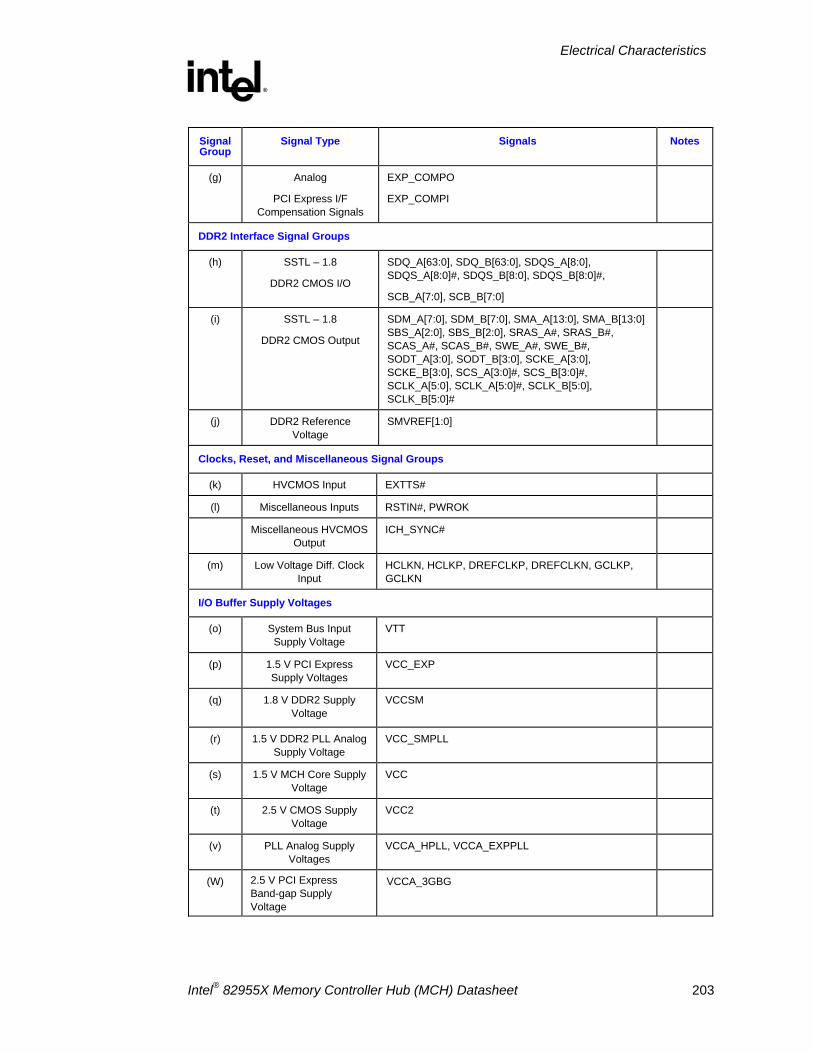
Electrical Characteristics
R
Intel® 82955X Memory Controller Hub (MCH) Datasheet 203
Signal Group
Signal Type Signals Notes
(g) Analog
PCI Express I/F Compensation Signals
EXP_COMPO
EXP_COMPI
DDR2 Interface Signal Groups
(h) SSTL – 1.8
DDR2 CMOS I/O
SDQ_A[63:0], SDQ_B[63:0], SDQS_A[8:0], SDQS_A[8:0]#, SDQS_B[8:0], SDQS_B[8:0]#,
SCB_A[7:0], SCB_B[7:0]
(i) SSTL – 1.8
DDR2 CMOS Output
SDM_A[7:0], SDM_B[7:0], SMA_A[13:0], SMA_B[13:0] SBS_A[2:0], SBS_B[2:0], SRAS_A#, SRAS_B#, SCAS_A#, SCAS_B#, SWE_A#, SWE_B#, SODT_A[3:0], SODT_B[3:0], SCKE_A[3:0], SCKE_B[3:0], SCS_A[3:0]#, SCS_B[3:0]#, SCLK_A[5:0], SCLK_A[5:0]#, SCLK_B[5:0], SCLK_B[5:0]#
(j) DDR2 Reference Voltage
SMVREF[1:0]
Clocks, Reset, and Miscellaneous Signal Groups
(k) HVCMOS Input EXTTS#
(l) Miscellaneous Inputs RSTIN#, PWROK
Miscellaneous HVCMOS Output
ICH_SYNC#
(m) Low Voltage Diff. Clock Input
HCLKN, HCLKP, DREFCLKP, DREFCLKN, GCLKP, GCLKN
I/O Buffer Supply Voltages
(o) System Bus Input Supply Voltage
VTT
(p) 1.5 V PCI Express Supply Voltages
VCC_EXP
(q) 1.8 V DDR2 Supply Voltage
VCCSM
(r) 1.5 V DDR2 PLL Analog Supply Voltage
VCC_SMPLL
(s) 1.5 V MCH Core Supply Voltage
VCC
(t) 2.5 V CMOS Supply Voltage
VCC2
(v) PLL Analog Supply Voltages
VCCA_HPLL, VCCA_EXPPLL
(W) 2.5 V PCI Express Band-gap Supply Voltage
VCCA_3GBG
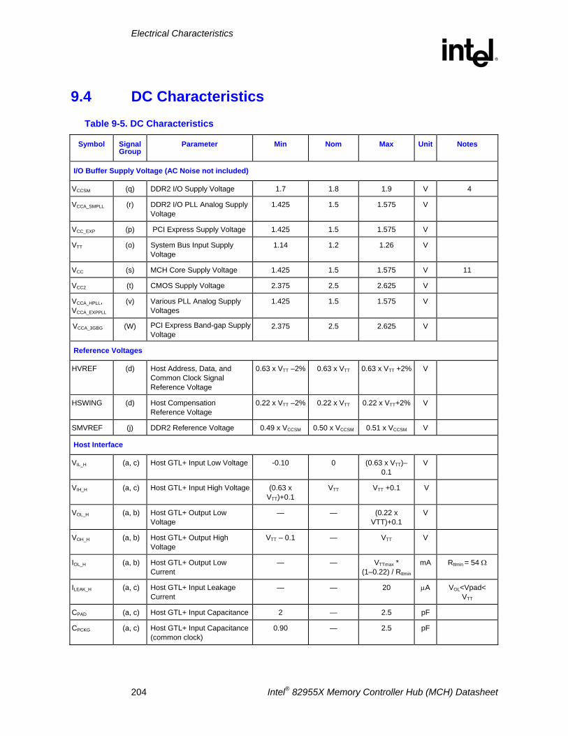
Electrical Characteristics
R
204 Intel® 82955X Memory Controller Hub (MCH) Datasheet
9.4 DC Characteristics Table 9-5. DC Characteristics
Symbol Signal Group
Parameter Min Nom Max Unit Notes
I/O Buffer Supply Voltage (AC Noise not included)
VCCSM (q) DDR2 I/O Supply Voltage 1.7 1.8 1.9 V 4
VCCA_SMPLL (r) DDR2 I/O PLL Analog Supply Voltage
1.425 1.5 1.575 V
VCC_EXP (p) PCI Express Supply Voltage 1.425 1.5 1.575 V
VTT (o) System Bus Input Supply Voltage
1.14 1.2 1.26 V
VCC (s) MCH Core Supply Voltage 1.425 1.5 1.575 V 11
VCC2 (t) CMOS Supply Voltage 2.375 2.5 2.625 V
VCCA_HPLL, VCCA_EXPPLL
(v) Various PLL Analog Supply Voltages
1.425 1.5 1.575 V
VCCA_3GBG (W) PCI Express Band-gap Supply Voltage
2.375 2.5 2.625 V
Reference Voltages
HVREF (d) Host Address, Data, and Common Clock Signal Reference Voltage
0.63 x VTT –2% 0.63 x VTT 0.63 x VTT +2% V
HSWING (d) Host Compensation Reference Voltage
0.22 x VTT –2% 0.22 x VTT 0.22 x VTT+2% V
SMVREF (j) DDR2 Reference Voltage 0.49 x VCCSM 0.50 x VCCSM 0.51 x VCCSM V
Host Interface
VIL_H (a, c) Host GTL+ Input Low Voltage -0.10 0 (0.63 x VTT)– 0.1
V
VIH_H (a, c) Host GTL+ Input High Voltage (0.63 x VTT)+0.1
VTT VTT +0.1 V
VOL_H (a, b) Host GTL+ Output Low Voltage
— — (0.22 x VTT)+0.1
V
VOH_H (a, b) Host GTL+ Output High Voltage
VTT – 0.1 — VTT V
IOL_H (a, b) Host GTL+ Output Low Current
— — VTTmax * (1–0.22) / Rttmin
mA Rttmin = 54 Ω
ILEAK_H (a, c) Host GTL+ Input Leakage Current
— — 20 µA VOL<Vpad< VTT
CPAD (a, c) Host GTL+ Input Capacitance 2 — 2.5 pF
CPCKG (a, c) Host GTL+ Input Capacitance (common clock)
0.90 — 2.5 pF
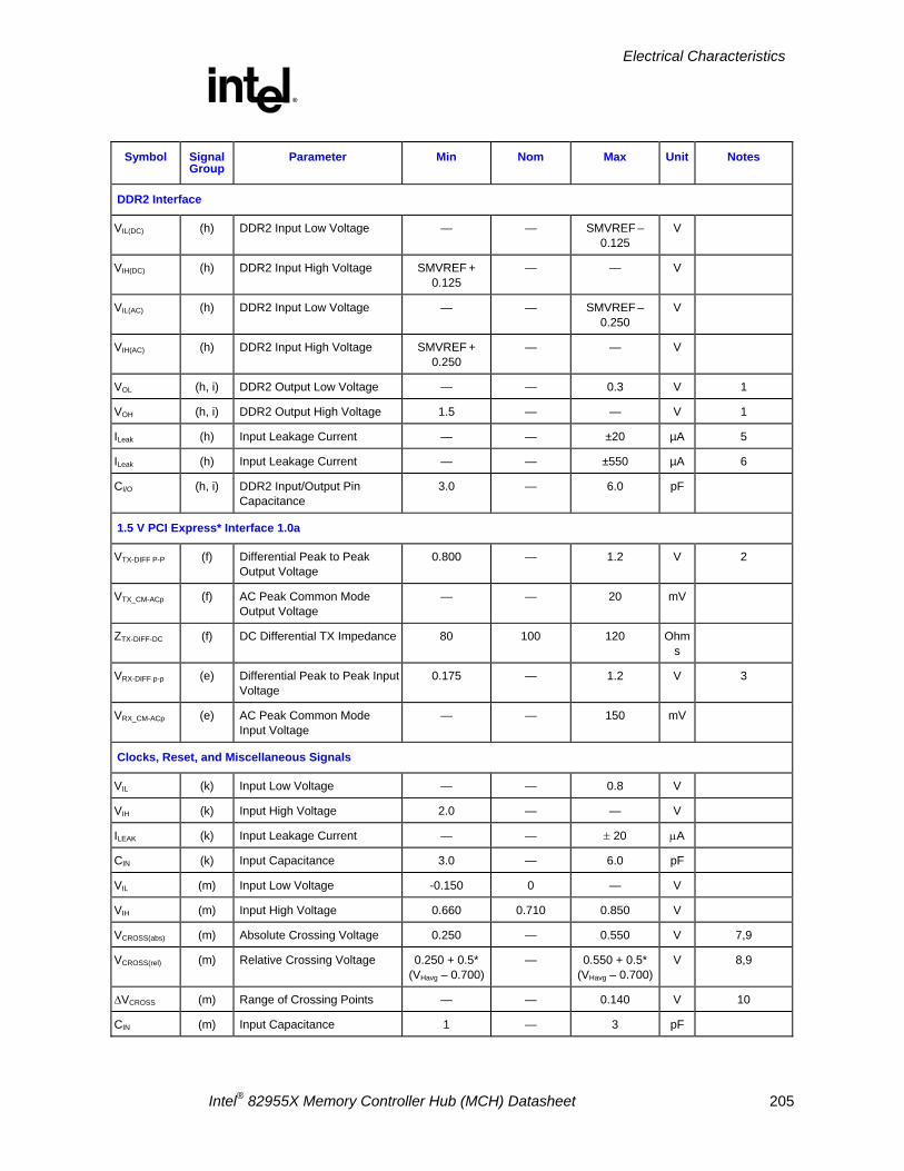
Electrical Characteristics
R
Intel® 82955X Memory Controller Hub (MCH) Datasheet 205
Symbol Signal Group
Parameter Min Nom Max Unit Notes
DDR2 Interface
VIL(DC) (h) DDR2 Input Low Voltage — — SMVREF – 0.125
V
VIH(DC) (h) DDR2 Input High Voltage SMVREF + 0.125
— — V
VIL(AC) (h) DDR2 Input Low Voltage — — SMVREF – 0.250
V
VIH(AC) (h) DDR2 Input High Voltage SMVREF + 0.250
— — V
VOL (h, i) DDR2 Output Low Voltage — — 0.3 V 1
VOH (h, i) DDR2 Output High Voltage 1.5 — — V 1
ILeak (h) Input Leakage Current — — ±20 µA 5
ILeak (h) Input Leakage Current — — ±550 µA 6
CI/O (h, i) DDR2 Input/Output Pin Capacitance
3.0 — 6.0 pF
1.5 V PCI Express* Interface 1.0a
VTX-DIFF P-P (f) Differential Peak to Peak Output Voltage
0.800 — 1.2 V 2
VTX_CM-ACp (f) AC Peak Common Mode Output Voltage
— — 20 mV
ZTX-DIFF-DC (f) DC Differential TX Impedance 80 100 120 Ohms
VRX-DIFF p-p (e) Differential Peak to Peak Input Voltage
0.175 — 1.2 V 3
VRX_CM-ACp (e) AC Peak Common Mode Input Voltage
— — 150 mV
Clocks, Reset, and Miscellaneous Signals
VIL (k) Input Low Voltage — — 0.8 V
VIH (k) Input High Voltage 2.0 — — V
ILEAK (k) Input Leakage Current — — ± 20 µA
CIN (k) Input Capacitance 3.0 — 6.0 pF
VIL (m) Input Low Voltage -0.150 0 — V
VIH (m) Input High Voltage 0.660 0.710 0.850 V
VCROSS(abs) (m) Absolute Crossing Voltage 0.250 — 0.550 V 7,9
VCROSS(rel) (m) Relative Crossing Voltage 0.250 + 0.5* (VHavg – 0.700)
— 0.550 + 0.5* (VHavg – 0.700)
V 8,9
∆VCROSS (m) Range of Crossing Points — — 0.140 V 10
CIN (m) Input Capacitance 1 — 3 pF
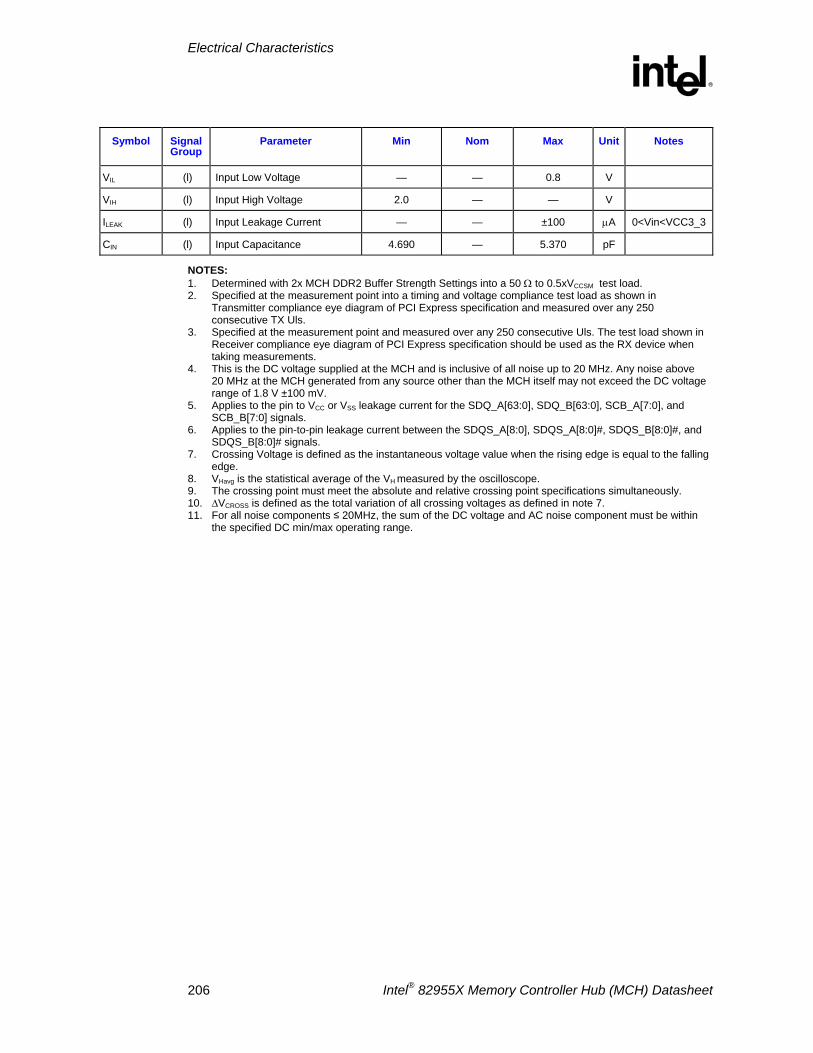
Electrical Characteristics
R
206 Intel® 82955X Memory Controller Hub (MCH) Datasheet
Symbol Signal Group
Parameter Min Nom Max Unit Notes
VIL (l) Input Low Voltage — — 0.8 V
VIH (l) Input High Voltage 2.0 — — V
ILEAK (l) Input Leakage Current — — ±100 µA 0<Vin<VCC3_3
CIN (l) Input Capacitance 4.690 — 5.370 pF
NOTES: 1. Determined with 2x MCH DDR2 Buffer Strength Settings into a 50 Ω to 0.5xVCCSM test load. 2. Specified at the measurement point into a timing and voltage compliance test load as shown in
Transmitter compliance eye diagram of PCI Express specification and measured over any 250 consecutive TX Uls.
3. Specified at the measurement point and measured over any 250 consecutive Uls. The test load shown in Receiver compliance eye diagram of PCI Express specification should be used as the RX device when taking measurements.
4. This is the DC voltage supplied at the MCH and is inclusive of all noise up to 20 MHz. Any noise above 20 MHz at the MCH generated from any source other than the MCH itself may not exceed the DC voltage range of 1.8 V ±100 mV.
5. Applies to the pin to VCC or VSS leakage current for the SDQ_A[63:0], SDQ_B[63:0], SCB_A[7:0], and SCB_B[7:0] signals.
6. Applies to the pin-to-pin leakage current between the SDQS_A[8:0], SDQS_A[8:0]#, SDQS_B[8:0]#, and SDQS_B[8:0]# signals.
7. Crossing Voltage is defined as the instantaneous voltage value when the rising edge is equal to the falling edge.
8. VHavg is the statistical average of the VH measured by the oscilloscope. 9. The crossing point must meet the absolute and relative crossing point specifications simultaneously. 10. ∆VCROSS is defined as the total variation of all crossing voltages as defined in note 7. 11. For all noise components ≤ 20MHz, the sum of the DC voltage and AC noise component must be within
the specified DC min/max operating range.
Ballout and Package Information
R
Intel® 82955X Memory Controller Hub (MCH) Datasheet 207
10 Ballout and Package Information This chapter provides the ballout and package information.
10.1 Ballout The following two figures diagram the MCH ballout for platforms using DDR2 system memory, as viewed from the top side of the package. The figures are broken into a left-side view and right-side view of the package.
Note: Balls that are listed as RSV are reserved. Board traces should Not be routed to these balls.
Note: Some balls marked as reserved (RSV) are used in XOR testing. See Chapter 11 for details.
Note: Some balls marked as reserved (RSV) can be used as test points. These are marked as RSV_TPx.
Note: Balls that are listed as NC are No Connects.
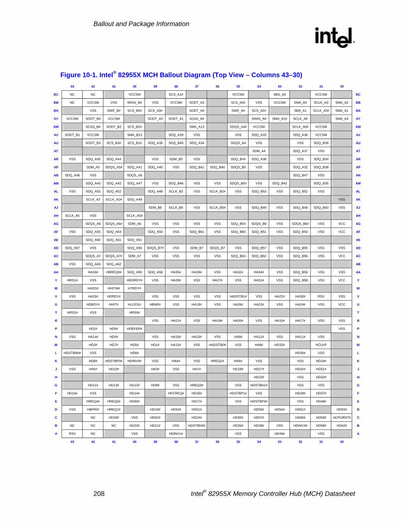
Ballout and Package Information
R
208 Intel® 82955X Memory Controller Hub (MCH) Datasheet
Figure 10-1. Intel® 82955X MCH Ballout Diagram (Top View – Columns 43–30) 43 42 41 40 39 38 37 36 35 34 33 32 31 30
BC NC NC VCCSM SCS_A1# VCCSM SBS_A0 VCCSM BC
BB NC VCCSM VSS SRAS_B# VSS VCCSM SODT_A2 SCS_A0# VSS VCCSM SMA_A0 SCLK_A3 SMA_A2 BB
BA VSS SWE_B# SCS_B0# SCS_A3# SODT_A0 SWE_A# SCS_A2# SBS_A1 SCLK_A3# SMA_A1 BA
AY VCCSM SODT_B0 VCCSM SODT_A3 SODT_A1 SCAS_A# SRAS_A# SMA_A10 SCLK_A0 SMA_A3 AY
AW SCAS_B# SODT_B2 SCS_B2# SMA_A13 SDQS_A4# VCCSM SCLK_A0# VCCSM AW
AV SODT_B1 VCCSM SMA_B13 SDQ_A39 VSS VSS SDQ_A33 SDQ_A36 VCCSM AV
AU SODT_B3 SCS_B3# SCS_B1# SDQ_A35 SDQ_B45 SDQ_A34 SDQS_A4 VSS VSS SDQ_B39 AU
AT SDM_A4 SDQ_A37 VSS AT
AR VSS SDQ_A45 SDQ_A44 VSS SDM_B5 VSS SDQ_B44 SDQ_A38 VSS SDQ_B34 AR
AP SDM_A5 SDQS_A5# SDQ_A41 SDQ_A40 VSS SDQ_B41 SDQ_B40 SDQS_B5 VSS SDQ_A32 SDQ_B38 AP
AN SDQ_A46 VSS SDQS_A5 SDQ_B47 VSS AN
AM SDQ_A43 SDQ_A42 SDQ_A47 VSS SDQ_B46 VSS VSS SDQS_B5# VSS SDQ_B42 SDQ_B35 AM
AL VSS SDQ_A53 SDQ_A52 SDQ_A48 SCLK_B2 VSS SCLK_B2# VSS SDQ_B53 VSS SDQ_B52 VSS AL
AK SCLK_A2 SCLK_A2# SDQ_A49 VSS AK
AJ SDM_B6 SCLK_B5 VSS SCLK_B5# VSS SDQ_B49 VSS SDQ_B48 SDQ_B43 VSS AJ
AH SCLK_A5 VSS SCLK_A5# AH
AG SDQS_A6 SDQS_A6# SDM_A6 VSS VSS VSS VSS SDQ_B54 SDQS_B6 VSS SDQS_B6# VSS VCC AG
AF VSS SDQ_A55 SDQ_A54 SDQ_A50 VSS SDQ_B61 VSS SDQ_B60 SDQ_B51 VSS SDQ_B50 VSS VCC AF
AE SDQ_A60 SDQ_A61 SDQ_A51 AE
AD SDQ_A57 VSS SDQ_A56 SDQS_B7# VSS SDM_B7 SDQS_B7 VSS SDQ_B57 VSS SDQ_B55 VSS VSS AD
AC SDQS_A7 SDQS_A7# SDM_A7 VSS VSS VSS VSS SDQ_B63 SDQ_B62 VSS SDQ_B56 VSS VCC AC
AB VSS SDQ_A63 SDQ_A62 AB
AA HA33# HBREQ0# SDQ_A59 SDQ_A58 HA35# HA29# VSS HA32# HA34# VSS SDQ_B59 VSS VSS AA
Y HRS1# VSS HEDRDY# VSS HA28# VSS HA27# VSS HA31# VSS SDQ_B58 VSS VCC Y
W HADS# HHITM# HTRDY# W
V VSS HA25# HDRDY# VSS VSS VSS VSS HADSTB1# VSS HA22# HA30# RSV VSS V
U HDBSY# HHIT# HLOCK# HBNR# VSS HA19# VSS HA26# HA23# VSS HA24# VSS VCC U
T HRS2# VSS HRS0# T
R VSS HA21# VSS HA18# HA20# VSS HA10# HA17# VSS VSS R
P HD2# HD0# HDEFER# VSS P
N VSS HA14# HD4# VSS HA16# HA15# VSS HA9# HA12# VSS HA11# VSS N
M HD3# HD7# HD5# HD1# HA13# VSS HADSTB0# VSS HA8# HD33# HCLKP M
L HDSTBN0# VSS HD6# HD30# VSS L
K HD8# HDSTBP0# HDINV0# VSS HA4# VSS HREQ2# HA6# VSS VSS HD34# K
J VSS HA5# HD10# HA3# VSS HA7# HD18# HD27# HD25# HD31# J
H HD23# VSS HD32# H
G HD11# HD13# HD12# HD9# VSS HREQ3# VSS HDSTBN1# VSS VSS G
F HD15# VSS HD14# HPCREQ# HD16# HDSTBP1# VSS HD29# HD37# F
E HREQ4# HREQ0# HD50# HD17# VSS HDSTBP3# VSS HD48# E
D VSS HBPRI# HREQ1# HD19# HD53# HD51# HD56# HD54# HD61# HD63# D
C NC HD20# VSS HD52# HD24# HD55# HD57# HD60# HD59# HCPURST# C
B NC NC NC HD22# HD21# VSS HDSTBN3# HD26# HD28# VSS HDINV3# HD58# HD62# B
A RSV NC VSS HDINV1# VSS HD49# VSS A
43 42 41 40 39 38 37 36 35 34 33 32 31 30
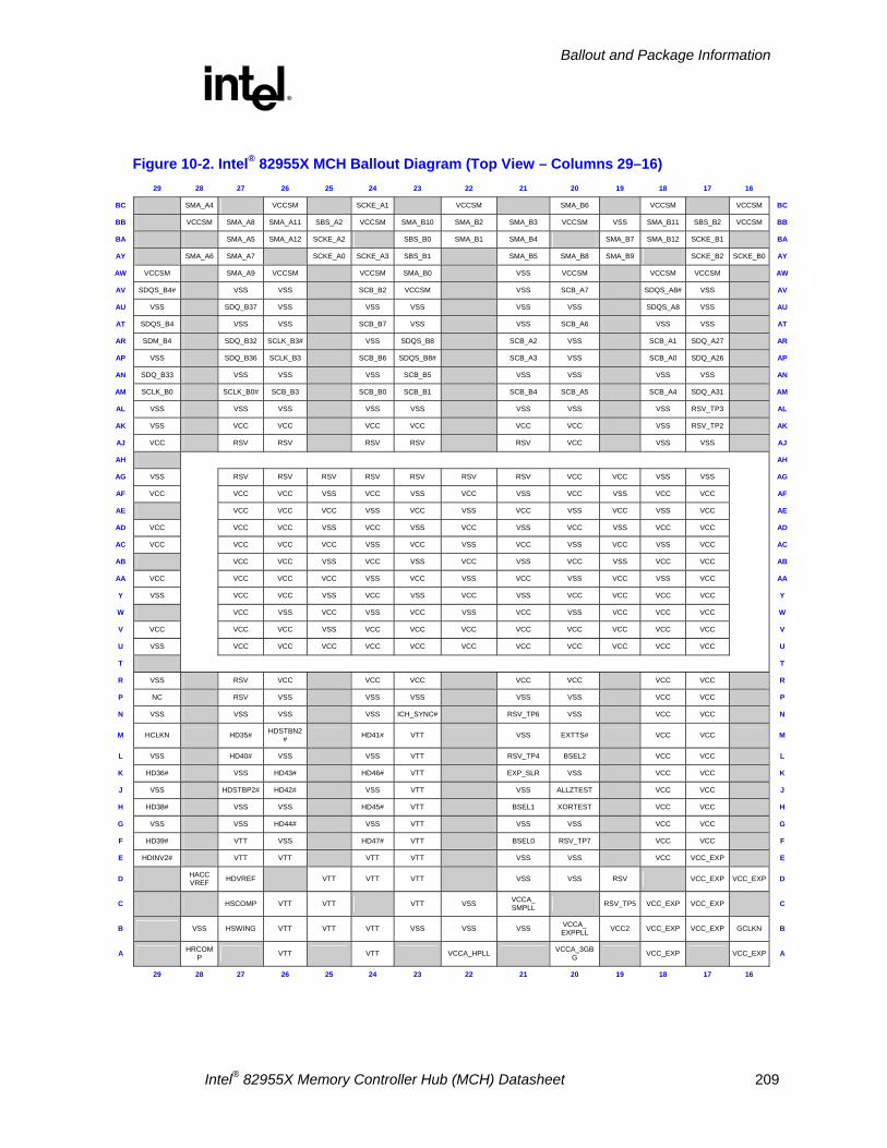
Ballout and Package Information
R
Intel® 82955X Memory Controller Hub (MCH) Datasheet 209
Figure 10-2. Intel® 82955X MCH Ballout Diagram (Top View – Columns 29–16) 29 28 27 26 25 24 23 22 21 20 19 18 17 16
BC SMA_A4 VCCSM SCKE_A1 VCCSM SMA_B6 VCCSM VCCSM BC
BB VCCSM SMA_A8 SMA_A11 SBS_A2 VCCSM SMA_B10 SMA_B2 SMA_B3 VCCSM VSS SMA_B11 SBS_B2 VCCSM BB
BA SMA_A5 SMA_A12 SCKE_A2 SBS_B0 SMA_B1 SMA_B4 SMA_B7 SMA_B12 SCKE_B1 BA
AY SMA_A6 SMA_A7 SCKE_A0 SCKE_A3 SBS_B1 SMA_B5 SMA_B8 SMA_B9 SCKE_B2 SCKE_B0 AY
AW VCCSM SMA_A9 VCCSM VCCSM SMA_B0 VSS VCCSM VCCSM VCCSM AW
AV SDQS_B4# VSS VSS SCB_B2 VCCSM VSS SCB_A7 SDQS_A8# VSS AV
AU VSS SDQ_B37 VSS VSS VSS VSS VSS SDQS_A8 VSS AU
AT SDQS_B4 VSS VSS SCB_B7 VSS VSS SCB_A6 VSS VSS AT
AR SDM_B4 SDQ_B32 SCLK_B3# VSS SDQS_B8 SCB_A2 VSS SCB_A1 SDQ_A27 AR
AP VSS SDQ_B36 SCLK_B3 SCB_B6 SDQS_B8# SCB_A3 VSS SCB_A0 SDQ_A26 AP
AN SDQ_B33 VSS VSS VSS SCB_B5 VSS VSS VSS VSS AN
AM SCLK_B0 SCLK_B0# SCB_B3 SCB_B0 SCB_B1 SCB_B4 SCB_A5 SCB_A4 SDQ_A31 AM
AL VSS VSS VSS VSS VSS VSS VSS VSS RSV_TP3 AL
AK VSS VCC VCC VCC VCC VCC VCC VSS RSV_TP2 AK
AJ VCC RSV RSV RSV RSV RSV VCC VSS VSS AJ
AH AH
AG VSS RSV RSV RSV RSV RSV RSV RSV VCC VCC VSS VSS AG
AF VCC VCC VCC VSS VCC VSS VCC VSS VCC VSS VCC VCC AF
AE VCC VCC VCC VSS VCC VSS VCC VSS VCC VSS VCC AE
AD VCC VCC VCC VSS VCC VSS VCC VSS VCC VSS VCC VCC AD
AC VCC VCC VCC VCC VSS VCC VSS VCC VSS VCC VSS VCC AC
AB VCC VCC VSS VCC VSS VCC VSS VCC VSS VCC VCC AB
AA VCC VCC VCC VCC VSS VCC VSS VCC VSS VCC VSS VCC AA
Y VSS VCC VCC VSS VCC VSS VCC VSS VCC VCC VCC VCC Y
W VCC VSS VCC VSS VCC VSS VCC VSS VCC VCC VCC W
V VCC VCC VCC VSS VCC VCC VCC VCC VCC VCC VCC VCC V
U VSS VCC VCC VCC VCC VCC VCC VCC VCC VCC VCC VCC U
T T
R VSS RSV VCC VCC VCC VCC VCC VCC VCC R
P NC RSV VSS VSS VSS VSS VSS VCC VCC P
N VSS VSS VSS VSS ICH_SYNC# RSV_TP6 VSS VCC VCC N
M HCLKN HD35# HDSTBN2# HD41# VTT VSS EXTTS# VCC VCC M
L VSS HD40# VSS VSS VTT RSV_TP4 BSEL2 VCC VCC L
K HD36# VSS HD43# HD46# VTT EXP_SLR VSS VCC VCC K
J VSS HDSTBP2# HD42# VSS VTT VSS ALLZTEST VCC VCC J
H HD38# VSS VSS HD45# VTT BSEL1 XORTEST VCC VCC H
G VSS VSS HD44# VSS VTT VSS VSS VCC VCC G
F HD39# VTT VSS HD47# VTT BSEL0 RSV_TP7 VCC VCC F
E HDINV2# VTT VTT VTT VTT VSS VSS VCC VCC_EXP E
D HACC VREF HDVREF VTT VTT VTT VSS VSS RSV VCC_EXP VCC_EXP D
C HSCOMP VTT VTT VTT VSS VCCA_ SMPLL RSV_TP5 VCC_EXP VCC_EXP C
B VSS HSWING VTT VTT VTT VSS VSS VSS VCCA_ EXPPLL VCC2 VCC_EXP VCC_EXP GCLKN B
A HRCOMP VTT VTT VCCA_HPLL VCCA_3GB
G VCC_EXP VCC_EXP A
29 28 27 26 25 24 23 22 21 20 19 18 17 16
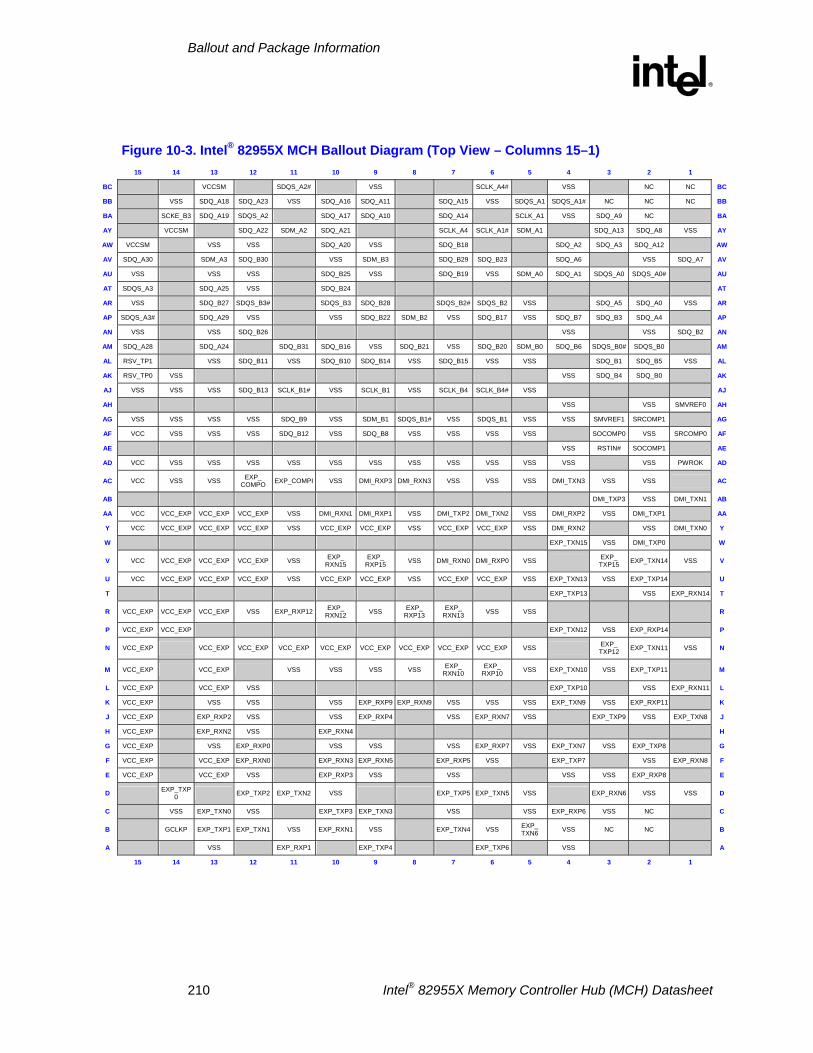
Ballout and Package Information
R
210 Intel® 82955X Memory Controller Hub (MCH) Datasheet
Figure 10-3. Intel® 82955X MCH Ballout Diagram (Top View – Columns 15–1) 15 14 13 12 11 10 9 8 7 6 5 4 3 2 1
BC VCCSM SDQS_A2# VSS SCLK_A4# VSS NC NC BC
BB VSS SDQ_A18 SDQ_A23 VSS SDQ_A16 SDQ_A11 SDQ_A15 VSS SDQS_A1 SDQS_A1# NC NC NC BB
BA SCKE_B3 SDQ_A19 SDQS_A2 SDQ_A17 SDQ_A10 SDQ_A14 SCLK_A1 VSS SDQ_A9 NC BA
AY VCCSM SDQ_A22 SDM_A2 SDQ_A21 SCLK_A4 SCLK_A1# SDM_A1 SDQ_A13 SDQ_A8 VSS AY
AW VCCSM VSS VSS SDQ_A20 VSS SDQ_B18 SDQ_A2 SDQ_A3 SDQ_A12 AW
AV SDQ_A30 SDM_A3 SDQ_B30 VSS SDM_B3 SDQ_B29 SDQ_B23 SDQ_A6 VSS SDQ_A7 AV
AU VSS VSS VSS SDQ_B25 VSS SDQ_B19 VSS SDM_A0 SDQ_A1 SDQS_A0 SDQS_A0# AU
AT SDQS_A3 SDQ_A25 VSS SDQ_B24 AT
AR VSS SDQ_B27 SDQS_B3# SDQS_B3 SDQ_B28 SDQS_B2# SDQS_B2 VSS SDQ_A5 SDQ_A0 VSS AR
AP SDQS_A3# SDQ_A29 VSS VSS SDQ_B22 SDM_B2 VSS SDQ_B17 VSS SDQ_B7 SDQ_B3 SDQ_A4 AP
AN VSS VSS SDQ_B26 VSS VSS SDQ_B2 AN
AM SDQ_A28 SDQ_A24 SDQ_B31 SDQ_B16 VSS SDQ_B21 VSS SDQ_B20 SDM_B0 SDQ_B6 SDQS_B0# SDQS_B0 AM
AL RSV_TP1 VSS SDQ_B11 VSS SDQ_B10 SDQ_B14 VSS SDQ_B15 VSS VSS SDQ_B1 SDQ_B5 VSS AL
AK RSV_TP0 VSS VSS SDQ_B4 SDQ_B0 AK
AJ VSS VSS VSS SDQ_B13 SCLK_B1# VSS SCLK_B1 VSS SCLK_B4 SCLK_B4# VSS AJ
AH VSS VSS SMVREF0 AH
AG VSS VSS VSS VSS SDQ_B9 VSS SDM_B1 SDQS_B1# VSS SDQS_B1 VSS VSS SMVREF1 SRCOMP1 AG
AF VCC VSS VSS VSS SDQ_B12 VSS SDQ_B8 VSS VSS VSS VSS SOCOMP0 VSS SRCOMP0 AF
AE VSS RSTIN# SOCOMP1 AE
AD VCC VSS VSS VSS VSS VSS VSS VSS VSS VSS VSS VSS VSS PWROK AD
AC VCC VSS VSS EXP_ COMPO EXP_COMPI VSS DMI_RXP3 DMI_RXN3 VSS VSS VSS DMI_TXN3 VSS VSS AC
AB DMI_TXP3 VSS DMI_TXN1 AB
AA VCC VCC_EXP VCC_EXP VCC_EXP VSS DMI_RXN1 DMI_RXP1 VSS DMI_TXP2 DMI_TXN2 VSS DMI_RXP2 VSS DMI_TXP1 AA
Y VCC VCC_EXP VCC_EXP VCC_EXP VSS VCC_EXP VCC_EXP VSS VCC_EXP VCC_EXP VSS DMI_RXN2 VSS DMI_TXN0 Y
W EXP_TXN15 VSS DMI_TXP0 W
V VCC VCC_EXP VCC_EXP VCC_EXP VSS EXP_ RXN15
EXP_ RXP15 VSS DMI_RXN0 DMI_RXP0 VSS EXP_
TXP15 EXP_TXN14 VSS V
U VCC VCC_EXP VCC_EXP VCC_EXP VSS VCC_EXP VCC_EXP VSS VCC_EXP VCC_EXP VSS EXP_TXN13 VSS EXP_TXP14 U
T EXP_TXP13 VSS EXP_RXN14 T
R VCC_EXP VCC_EXP VCC_EXP VSS EXP_RXP12 EXP_ RXN12 VSS EXP_
RXP13 EXP_
RXN13 VSS VSS R
P VCC_EXP VCC_EXP EXP_TXN12 VSS EXP_RXP14 P
N VCC_EXP VCC_EXP VCC_EXP VCC_EXP VCC_EXP VCC_EXP VCC_EXP VCC_EXP VCC_EXP VSS EXP_ TXP12 EXP_TXN11 VSS N
M VCC_EXP VCC_EXP VSS VSS VSS VSS EXP_ RXN10
EXP_ RXP10 VSS EXP_TXN10 VSS EXP_TXP11 M
L VCC_EXP VCC_EXP VSS EXP_TXP10 VSS EXP_RXN11 L
K VCC_EXP VSS VSS VSS EXP_RXP9 EXP_RXN9 VSS VSS VSS EXP_TXN9 VSS EXP_RXP11 K
J VCC_EXP EXP_RXP2 VSS VSS EXP_RXP4 VSS EXP_RXN7 VSS EXP_TXP9 VSS EXP_TXN8 J
H VCC_EXP EXP_RXN2 VSS EXP_RXN4 H
G VCC_EXP VSS EXP_RXP0 VSS VSS VSS EXP_RXP7 VSS EXP_TXN7 VSS EXP_TXP8 G
F VCC_EXP VCC_EXP EXP_RXN0 EXP_RXN3 EXP_RXN5 EXP_RXP5 VSS EXP_TXP7 VSS EXP_RXN8 F
E VCC_EXP VCC_EXP VSS EXP_RXP3 VSS VSS VSS VSS EXP_RXP8 E
D EXP_TXP0 EXP_TXP2 EXP_TXN2 VSS EXP_TXP5 EXP_TXN5 VSS EXP_RXN6 VSS VSS D
C VSS EXP_TXN0 VSS EXP_TXP3 EXP_TXN3 VSS VSS EXP_RXP6 VSS NC C
B GCLKP EXP_TXP1 EXP_TXN1 VSS EXP_RXN1 VSS EXP_TXN4 VSS EXP_ TXN6 VSS NC NC B
A VSS EXP_RXP1 EXP_TXP4 EXP_TXP6 VSS A
15 14 13 12 11 10 9 8 7 6 5 4 3 2 1
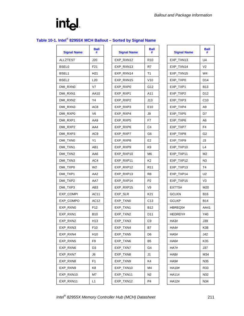
Ballout and Package Information
R
Intel® 82955X Memory Controller Hub (MCH) Datasheet 211
Table 10-1. Intel® 82955X MCH Ballout – Sorted by Signal Name
Signal Name Ball
#
ALLZTEST J20
BSEL0 F21
BSEL1 H21
BSEL2 L20
DMI_RXN0 V7
DMI_RXN1 AA10
DMI_RXN2 Y4
DMI_RXN3 AC8
DMI_RXP0 V6
DMI_RXP1 AA9
DMI_RXP2 AA4
DMI_RXP3 AC9
DMI_TXN0 Y1
DMI_TXN1 AB1
DMI_TXN2 AA6
DMI_TXN3 AC4
DMI_TXP0 W2
DMI_TXP1 AA2
DMI_TXP2 AA7
DMI_TXP3 AB3
EXP_COMPI AC11
EXP_COMPO AC12
EXP_RXN0 F12
EXP_RXN1 B10
EXP_RXN2 H13
EXP_RXN3 F10
EXP_RXN4 H10
EXP_RXN5 F9
EXP_RXN6 D3
EXP_RXN7 J6
EXP_RXN8 F1
EXP_RXN9 K8
EXP_RXN10 M7
EXP_RXN11 L1
Signal Name Ball
#
EXP_RXN12 R10
EXP_RXN13 R7
EXP_RXN14 T1
EXP_RXN15 V10
EXP_RXP0 G12
EXP_RXP1 A11
EXP_RXP2 J13
EXP_RXP3 E10
EXP_RXP4 J9
EXP_RXP5 F7
EXP_RXP6 C4
EXP_RXP7 G6
EXP_RXP8 E2
EXP_RXP9 K9
EXP_RXP10 M6
EXP_RXP11 K2
EXP_RXP12 R11
EXP_RXP13 R8
EXP_RXP14 P2
EXP_RXP15 V9
EXP_SLR K21
EXP_TXN0 C13
EXP_TXN1 B12
EXP_TXN2 D11
EXP_TXN3 C9
EXP_TXN4 B7
EXP_TXN5 D6
EXP_TXN6 B5
EXP_TXN7 G4
EXP_TXN8 J1
EXP_TXN9 K4
EXP_TXN10 M4
EXP_TXN11 N2
EXP_TXN12 P4
Signal Name Ball
#
EXP_TXN13 U4
EXP_TXN14 V2
EXP_TXN15 W4
EXP_TXP0 D14
EXP_TXP1 B13
EXP_TXP2 D12
EXP_TXP3 C10
EXP_TXP4 A9
EXP_TXP5 D7
EXP_TXP6 A6
EXP_TXP7 F4
EXP_TXP8 G2
EXP_TXP9 J3
EXP_TXP10 L4
EXP_TXP11 M2
EXP_TXP12 N3
EXP_TXP13 T4
EXP_TXP14 U2
EXP_TXP15 V3
EXTTS# M20
GCLKN B16
GCLKP B14
HBREQ0# AA41
HEDRDY# Y40
HA3# J39
HA4# K38
HA5# J42
HA6# K35
HA7# J37
HA8# M34
HA9# N35
HA10# R33
HA11# N32
HA12# N34
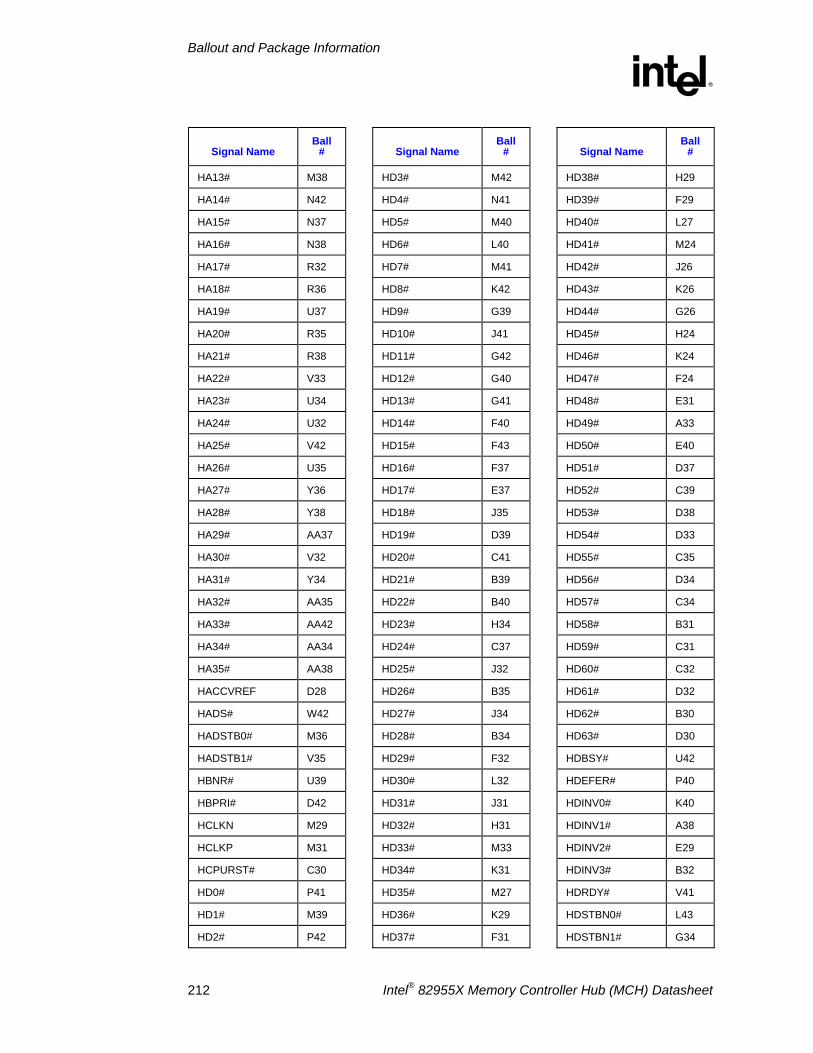
Ballout and Package Information
R
212 Intel® 82955X Memory Controller Hub (MCH) Datasheet
Signal Name Ball
#
HA13# M38
HA14# N42
HA15# N37
HA16# N38
HA17# R32
HA18# R36
HA19# U37
HA20# R35
HA21# R38
HA22# V33
HA23# U34
HA24# U32
HA25# V42
HA26# U35
HA27# Y36
HA28# Y38
HA29# AA37
HA30# V32
HA31# Y34
HA32# AA35
HA33# AA42
HA34# AA34
HA35# AA38
HACCVREF D28
HADS# W42
HADSTB0# M36
HADSTB1# V35
HBNR# U39
HBPRI# D42
HCLKN M29
HCLKP M31
HCPURST# C30
HD0# P41
HD1# M39
HD2# P42
Signal Name Ball
#
HD3# M42
HD4# N41
HD5# M40
HD6# L40
HD7# M41
HD8# K42
HD9# G39
HD10# J41
HD11# G42
HD12# G40
HD13# G41
HD14# F40
HD15# F43
HD16# F37
HD17# E37
HD18# J35
HD19# D39
HD20# C41
HD21# B39
HD22# B40
HD23# H34
HD24# C37
HD25# J32
HD26# B35
HD27# J34
HD28# B34
HD29# F32
HD30# L32
HD31# J31
HD32# H31
HD33# M33
HD34# K31
HD35# M27
HD36# K29
HD37# F31
Signal Name Ball
#
HD38# H29
HD39# F29
HD40# L27
HD41# M24
HD42# J26
HD43# K26
HD44# G26
HD45# H24
HD46# K24
HD47# F24
HD48# E31
HD49# A33
HD50# E40
HD51# D37
HD52# C39
HD53# D38
HD54# D33
HD55# C35
HD56# D34
HD57# C34
HD58# B31
HD59# C31
HD60# C32
HD61# D32
HD62# B30
HD63# D30
HDBSY# U42
HDEFER# P40
HDINV0# K40
HDINV1# A38
HDINV2# E29
HDINV3# B32
HDRDY# V41
HDSTBN0# L43
HDSTBN1# G34
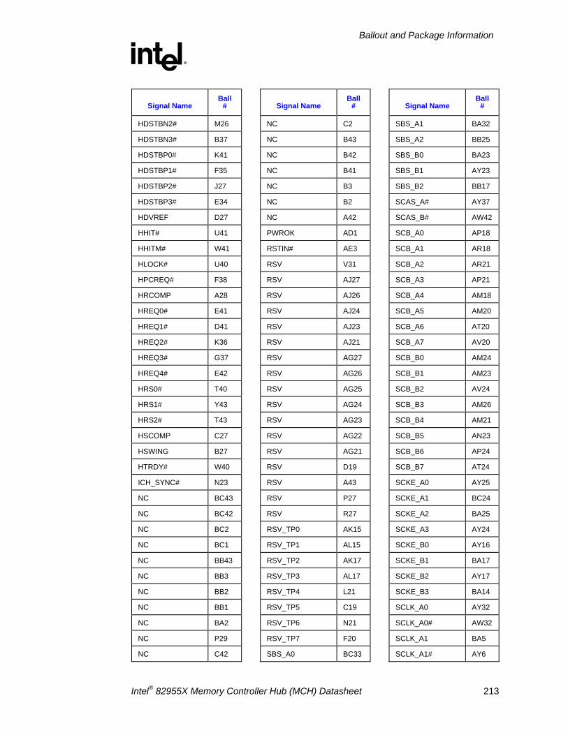
Ballout and Package Information
R
Intel® 82955X Memory Controller Hub (MCH) Datasheet 213
Signal Name Ball
#
HDSTBN2# M26
HDSTBN3# B37
HDSTBP0# K41
HDSTBP1# F35
HDSTBP2# J27
HDSTBP3# E34
HDVREF D27
HHIT# U41
HHITM# W41
HLOCK# U40
HPCREQ# F38
HRCOMP A28
HREQ0# E41
HREQ1# D41
HREQ2# K36
HREQ3# G37
HREQ4# E42
HRS0# T40
HRS1# Y43
HRS2# T43
HSCOMP C27
HSWING B27
HTRDY# W40
ICH_SYNC# N23
NC BC43
NC BC42
NC BC2
NC BC1
NC BB43
NC BB3
NC BB2
NC BB1
NC BA2
NC P29
NC C42
Signal Name Ball
#
NC C2
NC B43
NC B42
NC B41
NC B3
NC B2
NC A42
PWROK AD1
RSTIN# AE3
RSV V31
RSV AJ27
RSV AJ26
RSV AJ24
RSV AJ23
RSV AJ21
RSV AG27
RSV AG26
RSV AG25
RSV AG24
RSV AG23
RSV AG22
RSV AG21
RSV D19
RSV A43
RSV P27
RSV R27
RSV_TP0 AK15
RSV_TP1 AL15
RSV_TP2 AK17
RSV_TP3 AL17
RSV_TP4 L21
RSV_TP5 C19
RSV_TP6 N21
RSV_TP7 F20
SBS_A0 BC33
Signal Name Ball
#
SBS_A1 BA32
SBS_A2 BB25
SBS_B0 BA23
SBS_B1 AY23
SBS_B2 BB17
SCAS_A# AY37
SCAS_B# AW42
SCB_A0 AP18
SCB_A1 AR18
SCB_A2 AR21
SCB_A3 AP21
SCB_A4 AM18
SCB_A5 AM20
SCB_A6 AT20
SCB_A7 AV20
SCB_B0 AM24
SCB_B1 AM23
SCB_B2 AV24
SCB_B3 AM26
SCB_B4 AM21
SCB_B5 AN23
SCB_B6 AP24
SCB_B7 AT24
SCKE_A0 AY25
SCKE_A1 BC24
SCKE_A2 BA25
SCKE_A3 AY24
SCKE_B0 AY16
SCKE_B1 BA17
SCKE_B2 AY17
SCKE_B3 BA14
SCLK_A0 AY32
SCLK_A0# AW32
SCLK_A1 BA5
SCLK_A1# AY6
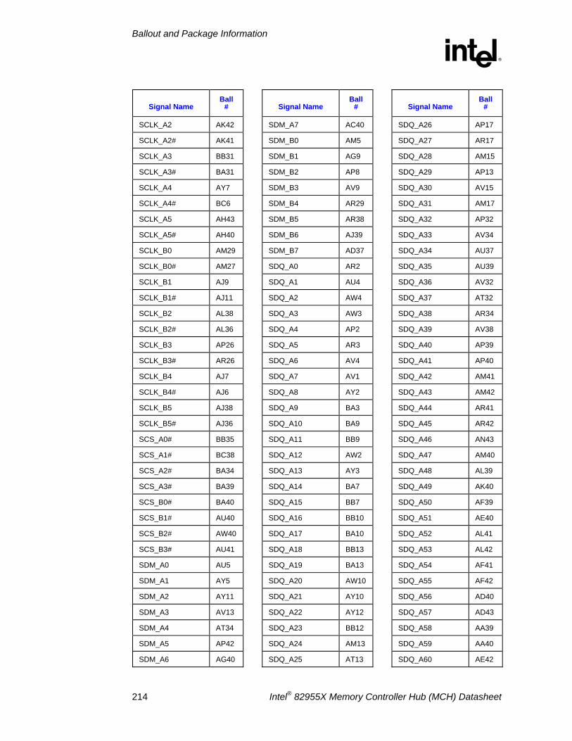
Ballout and Package Information
R
214 Intel® 82955X Memory Controller Hub (MCH) Datasheet
Signal Name Ball
#
SCLK_A2 AK42
SCLK_A2# AK41
SCLK_A3 BB31
SCLK_A3# BA31
SCLK_A4 AY7
SCLK_A4# BC6
SCLK_A5 AH43
SCLK_A5# AH40
SCLK_B0 AM29
SCLK_B0# AM27
SCLK_B1 AJ9
SCLK_B1# AJ11
SCLK_B2 AL38
SCLK_B2# AL36
SCLK_B3 AP26
SCLK_B3# AR26
SCLK_B4 AJ7
SCLK_B4# AJ6
SCLK_B5 AJ38
SCLK_B5# AJ36
SCS_A0# BB35
SCS_A1# BC38
SCS_A2# BA34
SCS_A3# BA39
SCS_B0# BA40
SCS_B1# AU40
SCS_B2# AW40
SCS_B3# AU41
SDM_A0 AU5
SDM_A1 AY5
SDM_A2 AY11
SDM_A3 AV13
SDM_A4 AT34
SDM_A5 AP42
SDM_A6 AG40
Signal Name Ball
#
SDM_A7 AC40
SDM_B0 AM5
SDM_B1 AG9
SDM_B2 AP8
SDM_B3 AV9
SDM_B4 AR29
SDM_B5 AR38
SDM_B6 AJ39
SDM_B7 AD37
SDQ_A0 AR2
SDQ_A1 AU4
SDQ_A2 AW4
SDQ_A3 AW3
SDQ_A4 AP2
SDQ_A5 AR3
SDQ_A6 AV4
SDQ_A7 AV1
SDQ_A8 AY2
SDQ_A9 BA3
SDQ_A10 BA9
SDQ_A11 BB9
SDQ_A12 AW2
SDQ_A13 AY3
SDQ_A14 BA7
SDQ_A15 BB7
SDQ_A16 BB10
SDQ_A17 BA10
SDQ_A18 BB13
SDQ_A19 BA13
SDQ_A20 AW10
SDQ_A21 AY10
SDQ_A22 AY12
SDQ_A23 BB12
SDQ_A24 AM13
SDQ_A25 AT13
Signal Name Ball
#
SDQ_A26 AP17
SDQ_A27 AR17
SDQ_A28 AM15
SDQ_A29 AP13
SDQ_A30 AV15
SDQ_A31 AM17
SDQ_A32 AP32
SDQ_A33 AV34
SDQ_A34 AU37
SDQ_A35 AU39
SDQ_A36 AV32
SDQ_A37 AT32
SDQ_A38 AR34
SDQ_A39 AV38
SDQ_A40 AP39
SDQ_A41 AP40
SDQ_A42 AM41
SDQ_A43 AM42
SDQ_A44 AR41
SDQ_A45 AR42
SDQ_A46 AN43
SDQ_A47 AM40
SDQ_A48 AL39
SDQ_A49 AK40
SDQ_A50 AF39
SDQ_A51 AE40
SDQ_A52 AL41
SDQ_A53 AL42
SDQ_A54 AF41
SDQ_A55 AF42
SDQ_A56 AD40
SDQ_A57 AD43
SDQ_A58 AA39
SDQ_A59 AA40
SDQ_A60 AE42
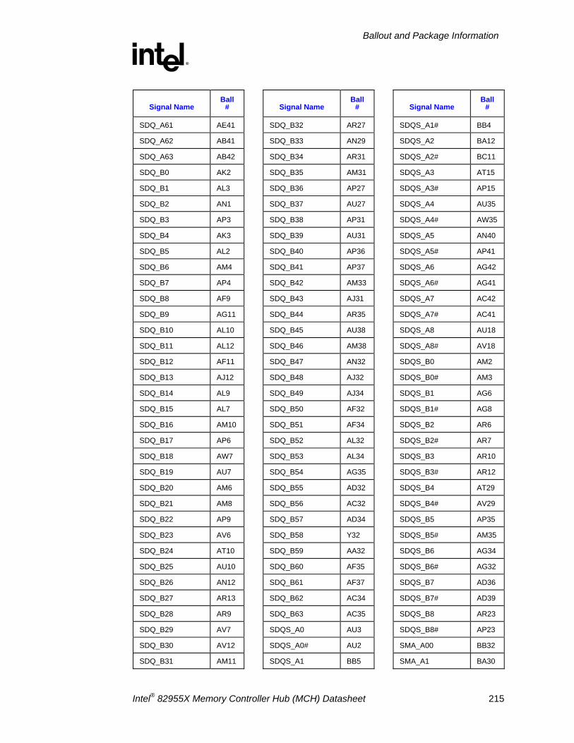
Ballout and Package Information
R
Intel® 82955X Memory Controller Hub (MCH) Datasheet 215
Signal Name Ball
#
SDQ_A61 AE41
SDQ_A62 AB41
SDQ_A63 AB42
SDQ_B0 AK2
SDQ_B1 AL3
SDQ_B2 AN1
SDQ_B3 AP3
SDQ_B4 AK3
SDQ_B5 AL2
SDQ_B6 AM4
SDQ_B7 AP4
SDQ_B8 AF9
SDQ_B9 AG11
SDQ_B10 AL10
SDQ_B11 AL12
SDQ_B12 AF11
SDQ_B13 AJ12
SDQ_B14 AL9
SDQ_B15 AL7
SDQ_B16 AM10
SDQ_B17 AP6
SDQ_B18 AW7
SDQ_B19 AU7
SDQ_B20 AM6
SDQ_B21 AM8
SDQ_B22 AP9
SDQ_B23 AV6
SDQ_B24 AT10
SDQ_B25 AU10
SDQ_B26 AN12
SDQ_B27 AR13
SDQ_B28 AR9
SDQ_B29 AV7
SDQ_B30 AV12
SDQ_B31 AM11
Signal Name Ball
#
SDQ_B32 AR27
SDQ_B33 AN29
SDQ_B34 AR31
SDQ_B35 AM31
SDQ_B36 AP27
SDQ_B37 AU27
SDQ_B38 AP31
SDQ_B39 AU31
SDQ_B40 AP36
SDQ_B41 AP37
SDQ_B42 AM33
SDQ_B43 AJ31
SDQ_B44 AR35
SDQ_B45 AU38
SDQ_B46 AM38
SDQ_B47 AN32
SDQ_B48 AJ32
SDQ_B49 AJ34
SDQ_B50 AF32
SDQ_B51 AF34
SDQ_B52 AL32
SDQ_B53 AL34
SDQ_B54 AG35
SDQ_B55 AD32
SDQ_B56 AC32
SDQ_B57 AD34
SDQ_B58 Y32
SDQ_B59 AA32
SDQ_B60 AF35
SDQ_B61 AF37
SDQ_B62 AC34
SDQ_B63 AC35
SDQS_A0 AU3
SDQS_A0# AU2
SDQS_A1 BB5
Signal Name Ball
#
SDQS_A1# BB4
SDQS_A2 BA12
SDQS_A2# BC11
SDQS_A3 AT15
SDQS_A3# AP15
SDQS_A4 AU35
SDQS_A4# AW35
SDQS_A5 AN40
SDQS_A5# AP41
SDQS_A6 AG42
SDQS_A6# AG41
SDQS_A7 AC42
SDQS_A7# AC41
SDQS_A8 AU18
SDQS_A8# AV18
SDQS_B0 AM2
SDQS_B0# AM3
SDQS_B1 AG6
SDQS_B1# AG8
SDQS_B2 AR6
SDQS_B2# AR7
SDQS_B3 AR10
SDQS_B3# AR12
SDQS_B4 AT29
SDQS_B4# AV29
SDQS_B5 AP35
SDQS_B5# AM35
SDQS_B6 AG34
SDQS_B6# AG32
SDQS_B7 AD36
SDQS_B7# AD39
SDQS_B8 AR23
SDQS_B8# AP23
SMA_A00 BB32
SMA_A1 BA30
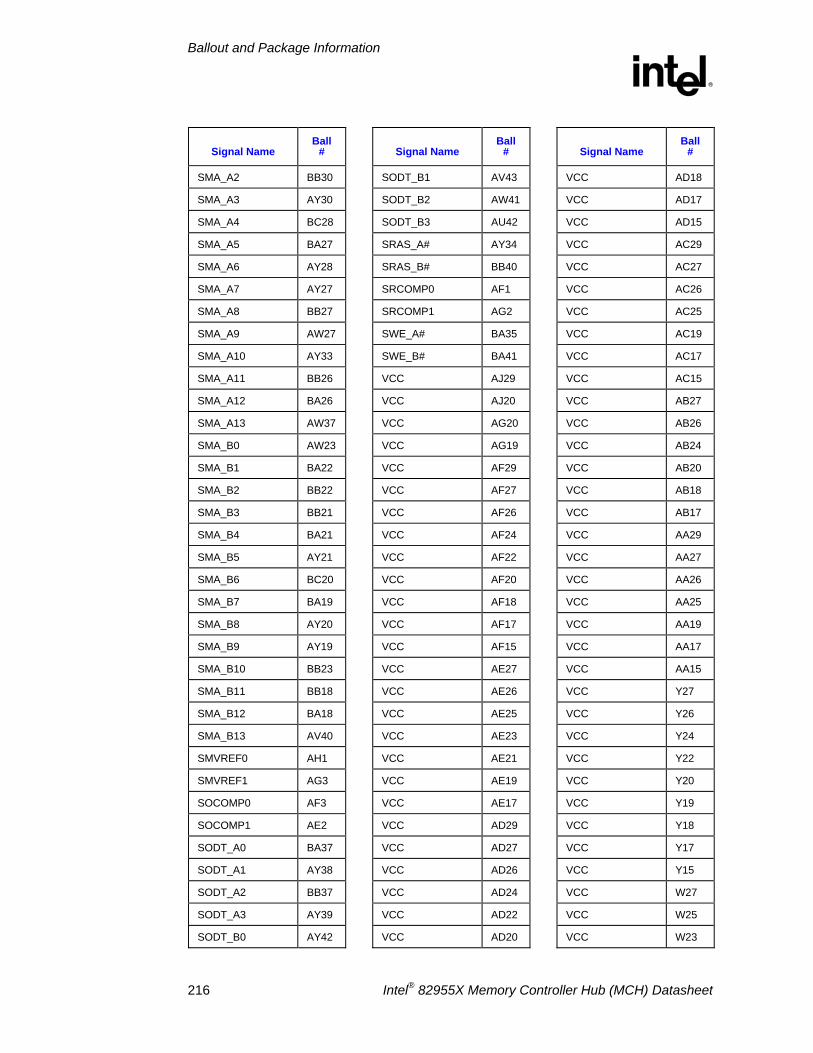
Ballout and Package Information
R
216 Intel® 82955X Memory Controller Hub (MCH) Datasheet
Signal Name Ball
#
SMA_A2 BB30
SMA_A3 AY30
SMA_A4 BC28
SMA_A5 BA27
SMA_A6 AY28
SMA_A7 AY27
SMA_A8 BB27
SMA_A9 AW27
SMA_A10 AY33
SMA_A11 BB26
SMA_A12 BA26
SMA_A13 AW37
SMA_B0 AW23
SMA_B1 BA22
SMA_B2 BB22
SMA_B3 BB21
SMA_B4 BA21
SMA_B5 AY21
SMA_B6 BC20
SMA_B7 BA19
SMA_B8 AY20
SMA_B9 AY19
SMA_B10 BB23
SMA_B11 BB18
SMA_B12 BA18
SMA_B13 AV40
SMVREF0 AH1
SMVREF1 AG3
SOCOMP0 AF3
SOCOMP1 AE2
SODT_A0 BA37
SODT_A1 AY38
SODT_A2 BB37
SODT_A3 AY39
SODT_B0 AY42
Signal Name Ball
#
SODT_B1 AV43
SODT_B2 AW41
SODT_B3 AU42
SRAS_A# AY34
SRAS_B# BB40
SRCOMP0 AF1
SRCOMP1 AG2
SWE_A# BA35
SWE_B# BA41
VCC AJ29
VCC AJ20
VCC AG20
VCC AG19
VCC AF29
VCC AF27
VCC AF26
VCC AF24
VCC AF22
VCC AF20
VCC AF18
VCC AF17
VCC AF15
VCC AE27
VCC AE26
VCC AE25
VCC AE23
VCC AE21
VCC AE19
VCC AE17
VCC AD29
VCC AD27
VCC AD26
VCC AD24
VCC AD22
VCC AD20
Signal Name Ball
#
VCC AD18
VCC AD17
VCC AD15
VCC AC29
VCC AC27
VCC AC26
VCC AC25
VCC AC19
VCC AC17
VCC AC15
VCC AB27
VCC AB26
VCC AB24
VCC AB20
VCC AB18
VCC AB17
VCC AA29
VCC AA27
VCC AA26
VCC AA25
VCC AA19
VCC AA17
VCC AA15
VCC Y27
VCC Y26
VCC Y24
VCC Y22
VCC Y20
VCC Y19
VCC Y18
VCC Y17
VCC Y15
VCC W27
VCC W25
VCC W23
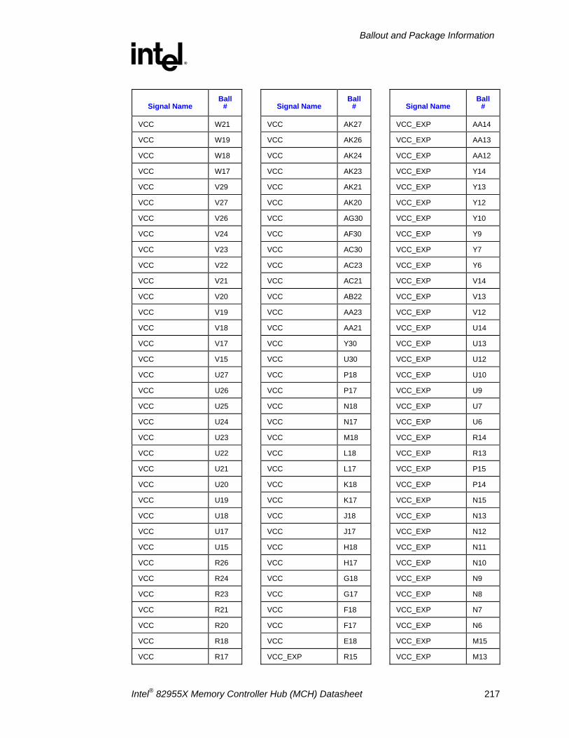
Ballout and Package Information
R
Intel® 82955X Memory Controller Hub (MCH) Datasheet 217
Signal Name Ball
#
VCC W21
VCC W19
VCC W18
VCC W17
VCC V29
VCC V27
VCC V26
VCC V24
VCC V23
VCC V22
VCC V21
VCC V20
VCC V19
VCC V18
VCC V17
VCC V15
VCC U27
VCC U26
VCC U25
VCC U24
VCC U23
VCC U22
VCC U21
VCC U20
VCC U19
VCC U18
VCC U17
VCC U15
VCC R26
VCC R24
VCC R23
VCC R21
VCC R20
VCC R18
VCC R17
Signal Name Ball
#
VCC AK27
VCC AK26
VCC AK24
VCC AK23
VCC AK21
VCC AK20
VCC AG30
VCC AF30
VCC AC30
VCC AC23
VCC AC21
VCC AB22
VCC AA23
VCC AA21
VCC Y30
VCC U30
VCC P18
VCC P17
VCC N18
VCC N17
VCC M18
VCC L18
VCC L17
VCC K18
VCC K17
VCC J18
VCC J17
VCC H18
VCC H17
VCC G18
VCC G17
VCC F18
VCC F17
VCC E18
VCC_EXP R15
Signal Name Ball
#
VCC_EXP AA14
VCC_EXP AA13
VCC_EXP AA12
VCC_EXP Y14
VCC_EXP Y13
VCC_EXP Y12
VCC_EXP Y10
VCC_EXP Y9
VCC_EXP Y7
VCC_EXP Y6
VCC_EXP V14
VCC_EXP V13
VCC_EXP V12
VCC_EXP U14
VCC_EXP U13
VCC_EXP U12
VCC_EXP U10
VCC_EXP U9
VCC_EXP U7
VCC_EXP U6
VCC_EXP R14
VCC_EXP R13
VCC_EXP P15
VCC_EXP P14
VCC_EXP N15
VCC_EXP N13
VCC_EXP N12
VCC_EXP N11
VCC_EXP N10
VCC_EXP N9
VCC_EXP N8
VCC_EXP N7
VCC_EXP N6
VCC_EXP M15
VCC_EXP M13
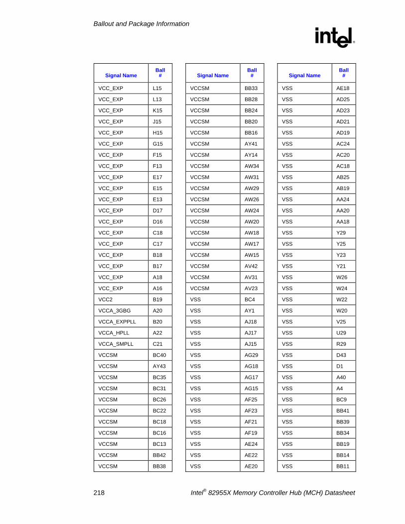
Ballout and Package Information
R
218 Intel® 82955X Memory Controller Hub (MCH) Datasheet
Signal Name Ball
#
VCC_EXP L15
VCC_EXP L13
VCC_EXP K15
VCC_EXP J15
VCC_EXP H15
VCC_EXP G15
VCC_EXP F15
VCC_EXP F13
VCC_EXP E17
VCC_EXP E15
VCC_EXP E13
VCC_EXP D17
VCC_EXP D16
VCC_EXP C18
VCC_EXP C17
VCC_EXP B18
VCC_EXP B17
VCC_EXP A18
VCC_EXP A16
VCC2 B19
VCCA_3GBG A20
VCCA_EXPPLL B20
VCCA_HPLL A22
VCCA_SMPLL C21
VCCSM BC40
VCCSM AY43
VCCSM BC35
VCCSM BC31
VCCSM BC26
VCCSM BC22
VCCSM BC18
VCCSM BC16
VCCSM BC13
VCCSM BB42
VCCSM BB38
Signal Name Ball
#
VCCSM BB33
VCCSM BB28
VCCSM BB24
VCCSM BB20
VCCSM BB16
VCCSM AY41
VCCSM AY14
VCCSM AW34
VCCSM AW31
VCCSM AW29
VCCSM AW26
VCCSM AW24
VCCSM AW20
VCCSM AW18
VCCSM AW17
VCCSM AW15
VCCSM AV42
VCCSM AV31
VCCSM AV23
VSS BC4
VSS AY1
VSS AJ18
VSS AJ17
VSS AJ15
VSS AG29
VSS AG18
VSS AG17
VSS AG15
VSS AF25
VSS AF23
VSS AF21
VSS AF19
VSS AE24
VSS AE22
VSS AE20
Signal Name Ball
#
VSS AE18
VSS AD25
VSS AD23
VSS AD21
VSS AD19
VSS AC24
VSS AC20
VSS AC18
VSS AB25
VSS AB19
VSS AA24
VSS AA20
VSS AA18
VSS Y29
VSS Y25
VSS Y23
VSS Y21
VSS W26
VSS W24
VSS W22
VSS W20
VSS V25
VSS U29
VSS R29
VSS D43
VSS D1
VSS A40
VSS A4
VSS BC9
VSS BB41
VSS BB39
VSS BB34
VSS BB19
VSS BB14
VSS BB11
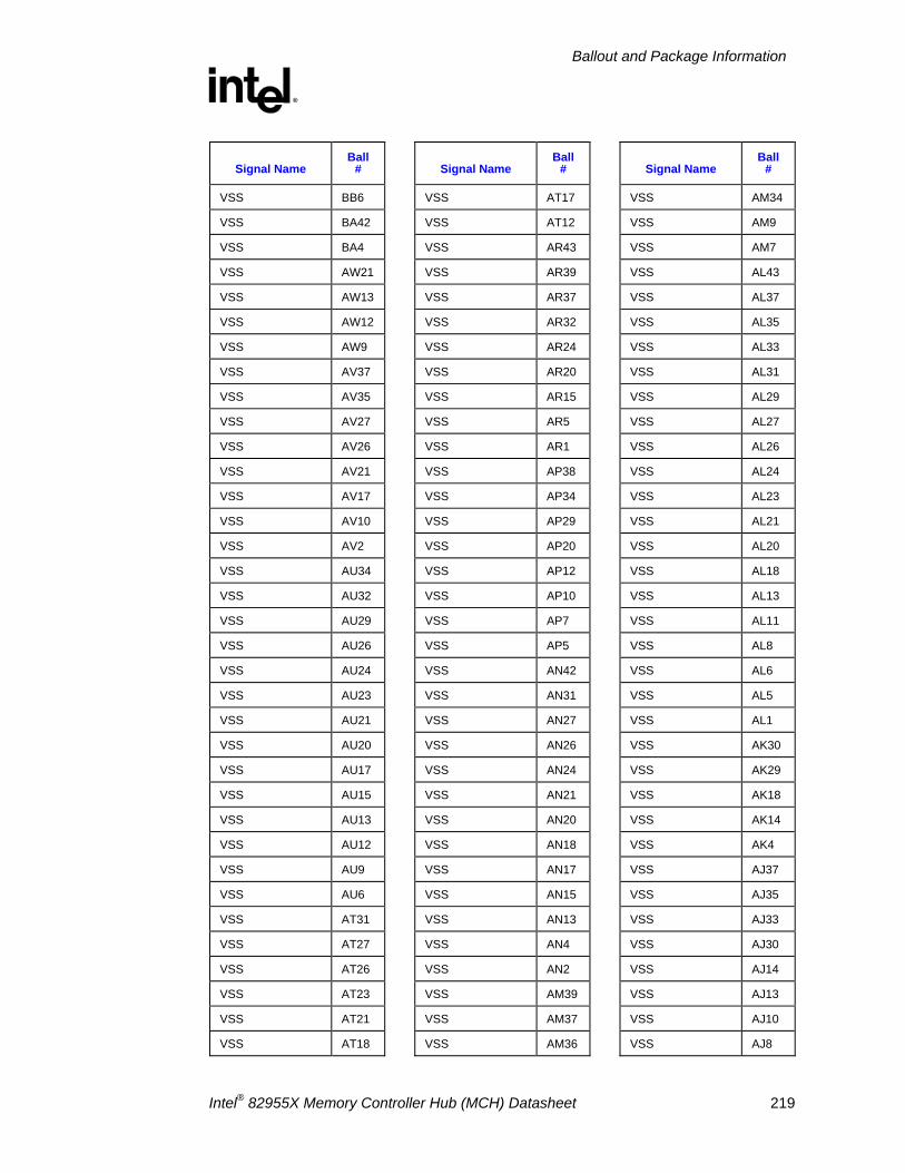
Ballout and Package Information
R
Intel® 82955X Memory Controller Hub (MCH) Datasheet 219
Signal Name Ball
#
VSS BB6
VSS BA42
VSS BA4
VSS AW21
VSS AW13
VSS AW12
VSS AW9
VSS AV37
VSS AV35
VSS AV27
VSS AV26
VSS AV21
VSS AV17
VSS AV10
VSS AV2
VSS AU34
VSS AU32
VSS AU29
VSS AU26
VSS AU24
VSS AU23
VSS AU21
VSS AU20
VSS AU17
VSS AU15
VSS AU13
VSS AU12
VSS AU9
VSS AU6
VSS AT31
VSS AT27
VSS AT26
VSS AT23
VSS AT21
VSS AT18
Signal Name Ball
#
VSS AT17
VSS AT12
VSS AR43
VSS AR39
VSS AR37
VSS AR32
VSS AR24
VSS AR20
VSS AR15
VSS AR5
VSS AR1
VSS AP38
VSS AP34
VSS AP29
VSS AP20
VSS AP12
VSS AP10
VSS AP7
VSS AP5
VSS AN42
VSS AN31
VSS AN27
VSS AN26
VSS AN24
VSS AN21
VSS AN20
VSS AN18
VSS AN17
VSS AN15
VSS AN13
VSS AN4
VSS AN2
VSS AM39
VSS AM37
VSS AM36
Signal Name Ball
#
VSS AM34
VSS AM9
VSS AM7
VSS AL43
VSS AL37
VSS AL35
VSS AL33
VSS AL31
VSS AL29
VSS AL27
VSS AL26
VSS AL24
VSS AL23
VSS AL21
VSS AL20
VSS AL18
VSS AL13
VSS AL11
VSS AL8
VSS AL6
VSS AL5
VSS AL1
VSS AK30
VSS AK29
VSS AK18
VSS AK14
VSS AK4
VSS AJ37
VSS AJ35
VSS AJ33
VSS AJ30
VSS AJ14
VSS AJ13
VSS AJ10
VSS AJ8
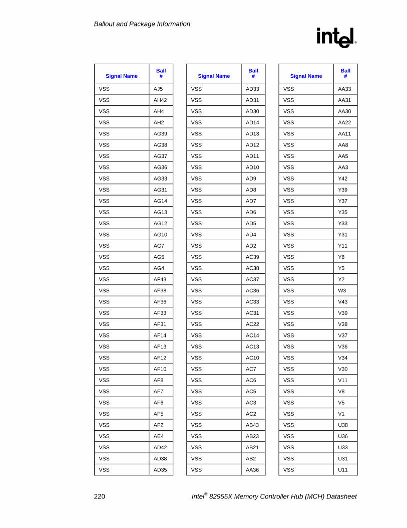
Ballout and Package Information
R
220 Intel® 82955X Memory Controller Hub (MCH) Datasheet
Signal Name Ball
#
VSS AJ5
VSS AH42
VSS AH4
VSS AH2
VSS AG39
VSS AG38
VSS AG37
VSS AG36
VSS AG33
VSS AG31
VSS AG14
VSS AG13
VSS AG12
VSS AG10
VSS AG7
VSS AG5
VSS AG4
VSS AF43
VSS AF38
VSS AF36
VSS AF33
VSS AF31
VSS AF14
VSS AF13
VSS AF12
VSS AF10
VSS AF8
VSS AF7
VSS AF6
VSS AF5
VSS AF2
VSS AE4
VSS AD42
VSS AD38
VSS AD35
Signal Name Ball
#
VSS AD33
VSS AD31
VSS AD30
VSS AD14
VSS AD13
VSS AD12
VSS AD11
VSS AD10
VSS AD9
VSS AD8
VSS AD7
VSS AD6
VSS AD5
VSS AD4
VSS AD2
VSS AC39
VSS AC38
VSS AC37
VSS AC36
VSS AC33
VSS AC31
VSS AC22
VSS AC14
VSS AC13
VSS AC10
VSS AC7
VSS AC6
VSS AC5
VSS AC3
VSS AC2
VSS AB43
VSS AB23
VSS AB21
VSS AB2
VSS AA36
Signal Name Ball
#
VSS AA33
VSS AA31
VSS AA30
VSS AA22
VSS AA11
VSS AA8
VSS AA5
VSS AA3
VSS Y42
VSS Y39
VSS Y37
VSS Y35
VSS Y33
VSS Y31
VSS Y11
VSS Y8
VSS Y5
VSS Y2
VSS W3
VSS V43
VSS V39
VSS V38
VSS V37
VSS V36
VSS V34
VSS V30
VSS V11
VSS V8
VSS V5
VSS V1
VSS U38
VSS U36
VSS U33
VSS U31
VSS U11
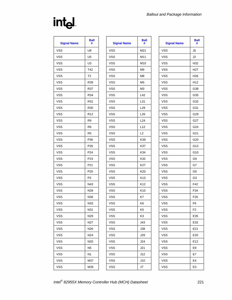
Ballout and Package Information
R
Intel® 82955X Memory Controller Hub (MCH) Datasheet 221
Signal Name Ball
#
VSS U8
VSS U5
VSS U3
VSS T42
VSS T2
VSS R39
VSS R37
VSS R34
VSS R31
VSS R30
VSS R12
VSS R9
VSS R6
VSS R5
VSS P30
VSS P26
VSS P24
VSS P23
VSS P21
VSS P20
VSS P3
VSS N43
VSS N39
VSS N36
VSS N33
VSS N31
VSS N29
VSS N27
VSS N26
VSS N24
VSS N20
VSS N5
VSS N1
VSS M37
VSS M35
Signal Name Ball
#
VSS M21
VSS M11
VSS M10
VSS M9
VSS M8
VSS M5
VSS M3
VSS L42
VSS L31
VSS L29
VSS L26
VSS L24
VSS L12
VSS L2
VSS K39
VSS K37
VSS K34
VSS K32
VSS K27
VSS K20
VSS K13
VSS K12
VSS K10
VSS K7
VSS K6
VSS K5
VSS K3
VSS J43
VSS J38
VSS J29
VSS J24
VSS J21
VSS J12
VSS J10
VSS J7
Signal Name Ball
#
VSS J5
VSS J2
VSS H32
VSS H27
VSS H26
VSS H12
VSS G38
VSS G35
VSS G32
VSS G31
VSS G29
VSS G27
VSS G24
VSS G21
VSS G20
VSS G13
VSS G10
VSS G9
VSS G7
VSS G5
VSS G3
VSS F42
VSS F34
VSS F26
VSS F6
VSS F2
VSS E35
VSS E32
VSS E21
VSS E20
VSS E12
VSS E9
VSS E7
VSS E4
VSS E3
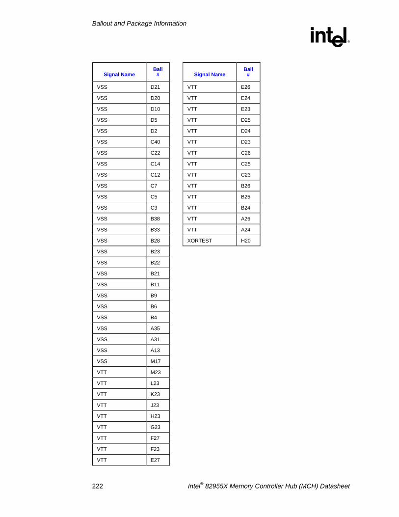
Ballout and Package Information
R
222 Intel® 82955X Memory Controller Hub (MCH) Datasheet
Signal Name Ball
#
VSS D21
VSS D20
VSS D10
VSS D5
VSS D2
VSS C40
VSS C22
VSS C14
VSS C12
VSS C7
VSS C5
VSS C3
VSS B38
VSS B33
VSS B28
VSS B23
VSS B22
VSS B21
VSS B11
VSS B9
VSS B6
VSS B4
VSS A35
VSS A31
VSS A13
VSS M17
VTT M23
VTT L23
VTT K23
VTT J23
VTT H23
VTT G23
VTT F27
VTT F23
VTT E27
Signal Name Ball
#
VTT E26
VTT E24
VTT E23
VTT D25
VTT D24
VTT D23
VTT C26
VTT C25
VTT C23
VTT B26
VTT B25
VTT B24
VTT A26
VTT A24
XORTEST H20
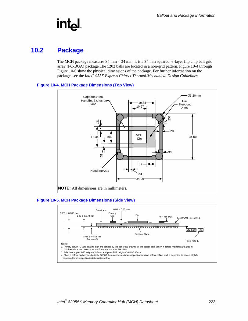
Ballout and Package Information
R
Intel® 82955X Memory Controller Hub (MCH) Datasheet 223
10.2 Package The MCH package measures 34 mm × 34 mm; it is a 34 mm squared, 6-layer flip chip ball grid array (FC-BGA) package The 1202 balls are located in a non-grid pattern. Figure 10-4 through Figure 10-6 show the physical dimensions of the package. For further information on the package, see the Intel® 955X Express Chipset Thermal/Mechanical Design Guidelines.
Figure 10-4. MCH Package Dimensions (Top View)
34.00
34.00
DieKeepout
Area
19.38
Capacitor Area,Handling Exclusion
Zone
MCHDie15.34 9.14
10.67
3.13.1
6.17
2.54
Ø5.20mm
2.30
3.0
2.0
Handling Area
NOTE: All dimensions are in millimeters.
Figure 10-5. MCH Package Dimensions (Side View)
Notes:1. Primary datum -C- and seating plan are defined by the spherical crow ns of the solder balls (show n before motherboard attach)2. All dimensions and tolerances conform to ANSI Y14.5M-19943. BGA has a pre-SMT height of 0.5mm and post-SMT height of 0.41-0.46mm4. Show n before motherboard attach; FCBGA has a convex (dome shaped) orientation before ref low and is expected to have a slightly concave (bow l shaped) orientation after ref low
0.20 –C–
Die
Substrate
0.435 ± 0.025 mmSee note 3
Seating Plane
1.92 ± 0.078 mm
See note 1.
DecoupCap 0.7 mm Max
2.355 ± 0.082 mm0.84 ± 0.05 mm
0.20 See note 4.
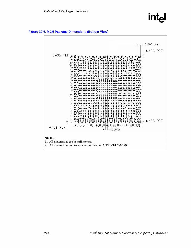
Ballout and Package Information
R
224 Intel® 82955X Memory Controller Hub (MCH) Datasheet
Figure 10-6. MCH Package Dimensions (Bottom View)
NOTES: 1 . All dimensions are in millimeters. 2. All dimensions and tolerances conform to ANSI Y14.5M-1994.
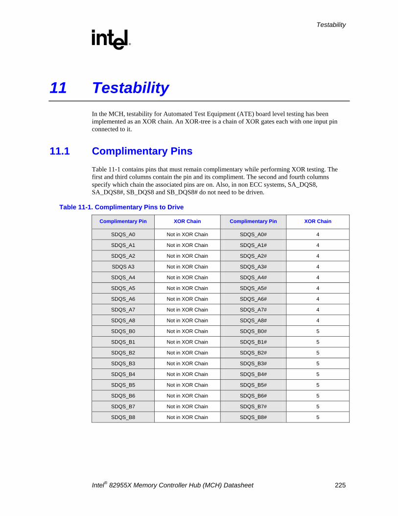
Testability
R
Intel® 82955X Memory Controller Hub (MCH) Datasheet 225
11 Testability In the MCH, testability for Automated Test Equipment (ATE) board level testing has been implemented as an XOR chain. An XOR-tree is a chain of XOR gates each with one input pin connected to it.
11.1 Complimentary Pins Table 11-1 contains pins that must remain complimentary while performing XOR testing. The first and third columns contain the pin and its compliment. The second and fourth columns specify which chain the associated pins are on. Also, in non ECC systems, SA_DQS8, SA_DQS8#, SB_DQS8 and SB_DQS8# do not need to be driven.
Table 11-1. Complimentary Pins to Drive
Complimentary Pin XOR Chain Complimentary Pin XOR Chain
SDQS_A0 Not in XOR Chain SDQS_A0# 4
SDQS_A1 Not in XOR Chain SDQS_A1# 4
SDQS_A2 Not in XOR Chain SDQS_A2# 4
SDQS A3 Not in XOR Chain SDQS_A3# 4
SDQS_A4 Not in XOR Chain SDQS_A4# 4
SDQS_A5 Not in XOR Chain SDQS_A5# 4
SDQS_A6 Not in XOR Chain SDQS_A6# 4
SDQS_A7 Not in XOR Chain SDQS_A7# 4
SDQS_A8 Not in XOR Chain SDQS_A8# 4
SDQS_B0 Not in XOR Chain SDQS_B0# 5
SDQS_B1 Not in XOR Chain SDQS_B1# 5
SDQS_B2 Not in XOR Chain SDQS_B2# 5
SDQS_B3 Not in XOR Chain SDQS_B3# 5
SDQS_B4 Not in XOR Chain SDQS_B4# 5
SDQS_B5 Not in XOR Chain SDQS_B5# 5
SDQS_B6 Not in XOR Chain SDQS_B6# 5
SDQS_B7 Not in XOR Chain SDQS_B7# 5
SDQS_B8 Not in XOR Chain SDQS_B8# 5
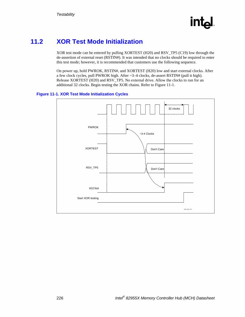
Testability
R
226 Intel® 82955X Memory Controller Hub (MCH) Datasheet
11.2 XOR Test Mode Initialization XOR test mode can be entered by pulling XORTEST (H20) and RSV_TP5 (C19) low through the de-assertion of external reset (RSTIN#). It was intended that no clocks should be required to enter this test mode; however, it is recommended that customers use the following sequence.
On power up, hold PWROK, RSTIN#, and XORTEST (H20) low and start external clocks. After a few clock cycles, pull PWROK high. After ~3–4 clocks, de-assert RSTIN# (pull it high). Release XORTEST (H20) and RSV_TP5. No external drive. Allow the clocks to run for an additional 32 clocks. Begin testing the XOR chains. Refer to Figure 11-1.
Figure 11-1. XOR Test Mode Initialization Cycles
PWROK
XORTEST
RSV_TP5
Don’t Care
Don’t Care
RSTIN#
~3-4 Clocks
32 clocks
Start XOR testing
XOR_Chain_Tim
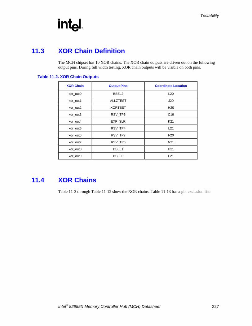
Testability
R
Intel® 82955X Memory Controller Hub (MCH) Datasheet 227
11.3 XOR Chain Definition The MCH chipset has 10 XOR chains. The XOR chain outputs are driven out on the following output pins. During full width testing, XOR chain outputs will be visible on both pins.
Table 11-2. XOR Chain Outputs
XOR Chain Output Pins Coordinate Location
xor_out0 BSEL2 L20
xor_out1 ALLZTEST J20
xor_out2 XORTEST H20
xor_out3 RSV_TP5 C19
xor_out4 EXP_SLR K21
xor_out5 RSV_TP4 L21
xor_out6 RSV_TP7 F20
xor_out7 RSV_TP6 N21
xor_out8 BSEL1 H21
xor_out9 BSEL0 F21
11.4 XOR Chains Table 11-3 through Table 11-12 show the XOR chains. Table 11-13 has a pin exclusion list.
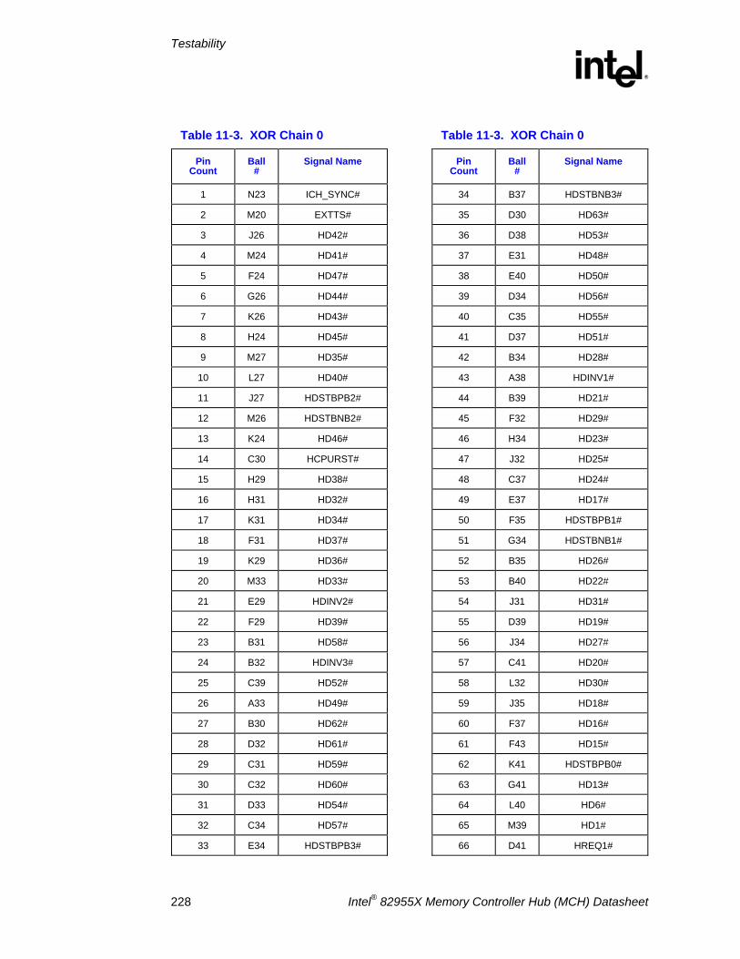
Testability
R
228 Intel® 82955X Memory Controller Hub (MCH) Datasheet
Table 11-3. XOR Chain 0
Pin Count
Ball #
Signal Name
1 N23 ICH_SYNC#
2 M20 EXTTS#
3 J26 HD42#
4 M24 HD41#
5 F24 HD47#
6 G26 HD44#
7 K26 HD43#
8 H24 HD45#
9 M27 HD35#
10 L27 HD40#
11 J27 HDSTBPB2#
12 M26 HDSTBNB2#
13 K24 HD46#
14 C30 HCPURST#
15 H29 HD38#
16 H31 HD32#
17 K31 HD34#
18 F31 HD37#
19 K29 HD36#
20 M33 HD33#
21 E29 HDINV2#
22 F29 HD39#
23 B31 HD58#
24 B32 HDINV3#
25 C39 HD52#
26 A33 HD49#
27 B30 HD62#
28 D32 HD61#
29 C31 HD59#
30 C32 HD60#
31 D33 HD54#
32 C34 HD57#
33 E34 HDSTBPB3#
Table 11-3. XOR Chain 0
Pin Count
Ball #
Signal Name
34 B37 HDSTBNB3#
35 D30 HD63#
36 D38 HD53#
37 E31 HD48#
38 E40 HD50#
39 D34 HD56#
40 C35 HD55#
41 D37 HD51#
42 B34 HD28#
43 A38 HDINV1#
44 B39 HD21#
45 F32 HD29#
46 H34 HD23#
47 J32 HD25#
48 C37 HD24#
49 E37 HD17#
50 F35 HDSTBPB1#
51 G34 HDSTBNB1#
52 B35 HD26#
53 B40 HD22#
54 J31 HD31#
55 D39 HD19#
56 J34 HD27#
57 C41 HD20#
58 L32 HD30#
59 J35 HD18#
60 F37 HD16#
61 F43 HD15#
62 K41 HDSTBPB0#
63 G41 HD13#
64 L40 HD6#
65 M39 HD1#
66 D41 HREQ1#
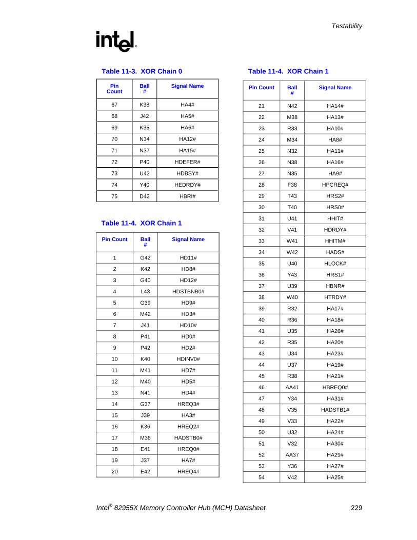
Testability
R
Intel® 82955X Memory Controller Hub (MCH) Datasheet 229
Table 11-3. XOR Chain 0
Pin Count
Ball #
Signal Name
67 K38 HA4#
68 J42 HA5#
69 K35 HA6#
70 N34 HA12#
71 N37 HA15#
72 P40 HDEFER#
73 U42 HDBSY#
74 Y40 HEDRDY#
75 D42 HBRI#
Table 11-4. XOR Chain 1
Pin Count Ball #
Signal Name
1 G42 HD11#
2 K42 HD8#
3 G40 HD12#
4 L43 HDSTBNB0#
5 G39 HD9#
6 M42 HD3#
7 J41 HD10#
8 P41 HD0#
9 P42 HD2#
10 K40 HDINV0#
11 M41 HD7#
12 M40 HD5#
13 N41 HD4#
14 G37 HREQ3#
15 J39 HA3#
16 K36 HREQ2#
17 M36 HADSTB0#
18 E41 HREQ0#
19 J37 HA7#
20 E42 HREQ4#
Table 11-4. XOR Chain 1
Pin Count Ball #
Signal Name
21 N42 HA14#
22 M38 HA13#
23 R33 HA10#
24 M34 HA8#
25 N32 HA11#
26 N38 HA16#
27 N35 HA9#
28 F38 HPCREQ#
29 T43 HRS2#
30 T40 HRS0#
31 U41 HHIT#
32 V41 HDRDY#
33 W41 HHITM#
34 W42 HADS#
35 U40 HLOCK#
36 Y43 HRS1#
37 U39 HBNR#
38 W40 HTRDY#
39 R32 HA17#
40 R36 HA18#
41 U35 HA26#
42 R35 HA20#
43 U34 HA23#
44 U37 HA19#
45 R38 HA21#
46 AA41 HBREQ0#
47 Y34 HA31#
48 V35 HADSTB1#
49 V33 HA22#
50 U32 HA24#
51 V32 HA30#
52 AA37 HA29#
53 Y36 HA27#
54 V42 HA25#
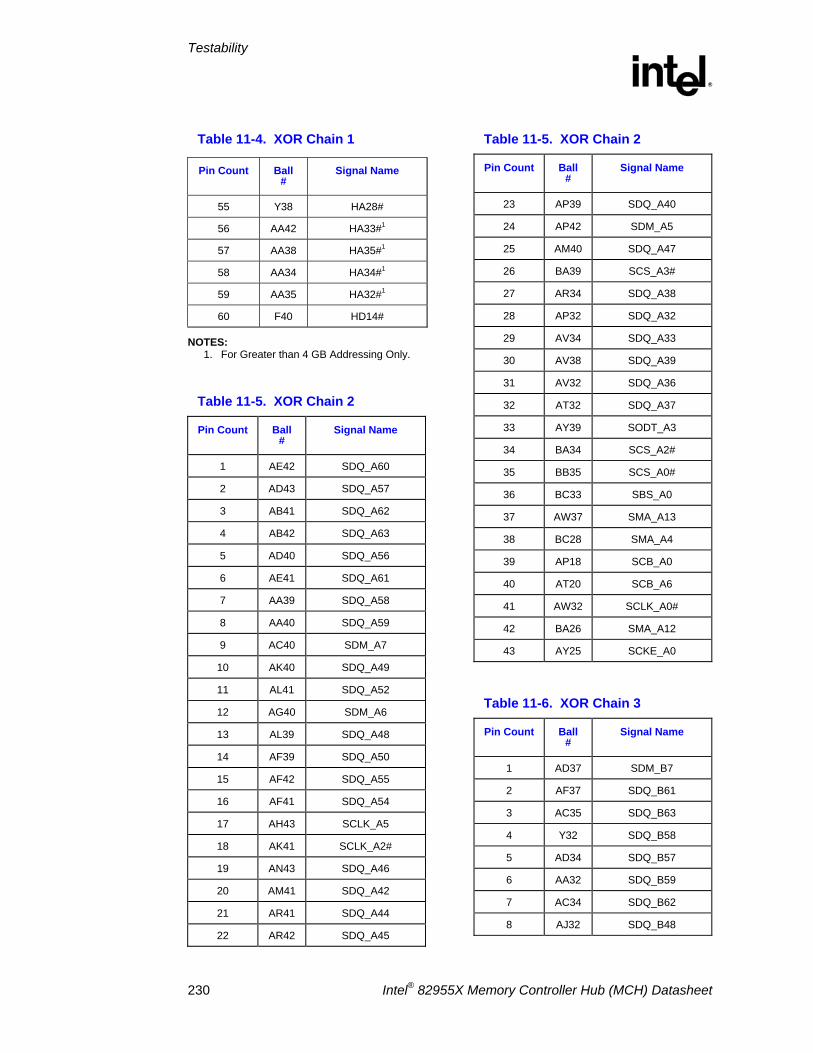
Testability
R
230 Intel® 82955X Memory Controller Hub (MCH) Datasheet
Table 11-4. XOR Chain 1
Pin Count Ball #
Signal Name
55 Y38 HA28#
56 AA42 HA33#1
57 AA38 HA35#1
58 AA34 HA34#1
59 AA35 HA32#1
60 F40 HD14#
NOTES: 1. For Greater than 4 GB Addressing Only.
Table 11-5. XOR Chain 2
Pin Count Ball #
Signal Name
1 AE42 SDQ_A60
2 AD43 SDQ_A57
3 AB41 SDQ_A62
4 AB42 SDQ_A63
5 AD40 SDQ_A56
6 AE41 SDQ_A61
7 AA39 SDQ_A58
8 AA40 SDQ_A59
9 AC40 SDM_A7
10 AK40 SDQ_A49
11 AL41 SDQ_A52
12 AG40 SDM_A6
13 AL39 SDQ_A48
14 AF39 SDQ_A50
15 AF42 SDQ_A55
16 AF41 SDQ_A54
17 AH43 SCLK_A5
18 AK41 SCLK_A2#
19 AN43 SDQ_A46
20 AM41 SDQ_A42
21 AR41 SDQ_A44
22 AR42 SDQ_A45
Table 11-5. XOR Chain 2
Pin Count Ball #
Signal Name
23 AP39 SDQ_A40
24 AP42 SDM_A5
25 AM40 SDQ_A47
26 BA39 SCS_A3#
27 AR34 SDQ_A38
28 AP32 SDQ_A32
29 AV34 SDQ_A33
30 AV38 SDQ_A39
31 AV32 SDQ_A36
32 AT32 SDQ_A37
33 AY39 SODT_A3
34 BA34 SCS_A2#
35 BB35 SCS_A0#
36 BC33 SBS_A0
37 AW37 SMA_A13
38 BC28 SMA_A4
39 AP18 SCB_A0
40 AT20 SCB_A6
41 AW32 SCLK_A0#
42 BA26 SMA_A12
43 AY25 SCKE_A0
Table 11-6. XOR Chain 3
Pin Count Ball #
Signal Name
1 AD37 SDM_B7
2 AF37 SDQ_B61
3 AC35 SDQ_B63
4 Y32 SDQ_B58
5 AD34 SDQ_B57
6 AA32 SDQ_B59
7 AC34 SDQ_B62
8 AJ32 SDQ_B48
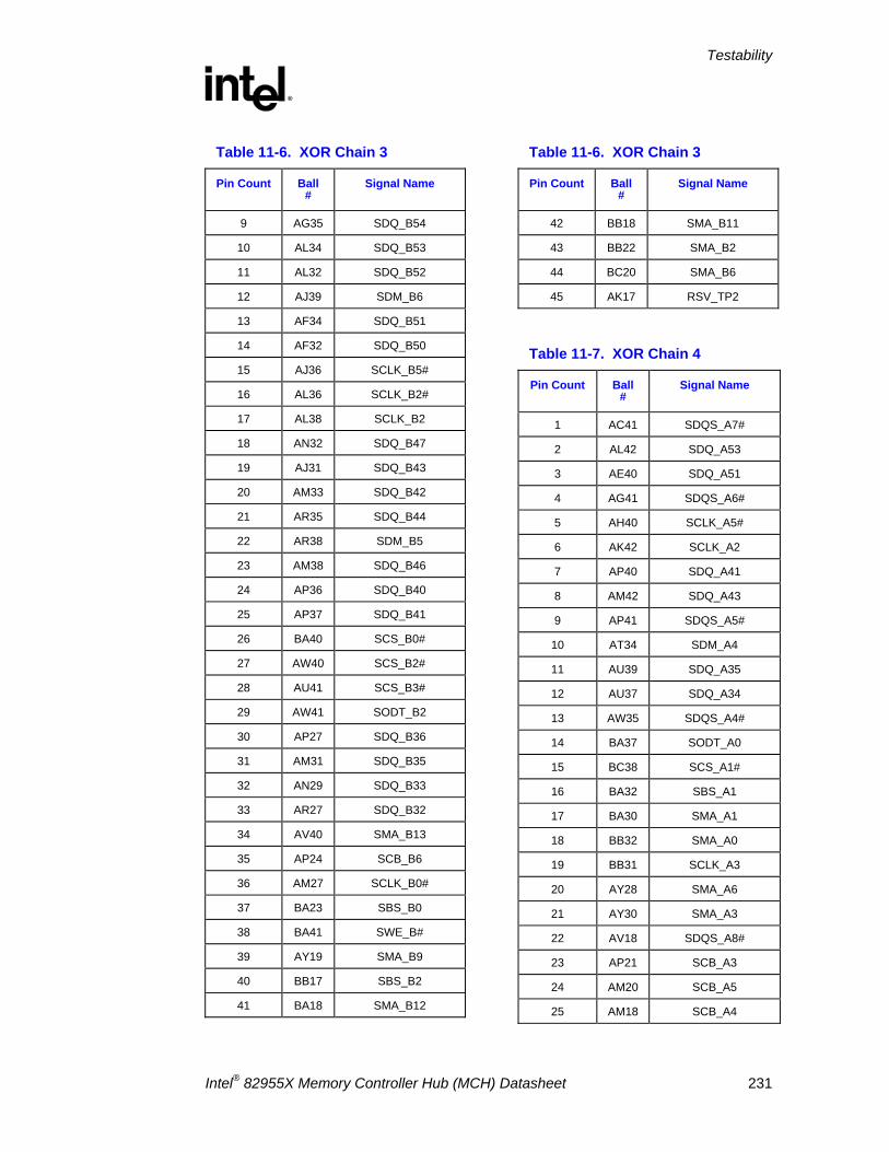
Testability
R
Intel® 82955X Memory Controller Hub (MCH) Datasheet 231
Table 11-6. XOR Chain 3
Pin Count Ball #
Signal Name
9 AG35 SDQ_B54
10 AL34 SDQ_B53
11 AL32 SDQ_B52
12 AJ39 SDM_B6
13 AF34 SDQ_B51
14 AF32 SDQ_B50
15 AJ36 SCLK_B5#
16 AL36 SCLK_B2#
17 AL38 SCLK_B2
18 AN32 SDQ_B47
19 AJ31 SDQ_B43
20 AM33 SDQ_B42
21 AR35 SDQ_B44
22 AR38 SDM_B5
23 AM38 SDQ_B46
24 AP36 SDQ_B40
25 AP37 SDQ_B41
26 BA40 SCS_B0#
27 AW40 SCS_B2#
28 AU41 SCS_B3#
29 AW41 SODT_B2
30 AP27 SDQ_B36
31 AM31 SDQ_B35
32 AN29 SDQ_B33
33 AR27 SDQ_B32
34 AV40 SMA_B13
35 AP24 SCB_B6
36 AM27 SCLK_B0#
37 BA23 SBS_B0
38 BA41 SWE_B#
39 AY19 SMA_B9
40 BB17 SBS_B2
41 BA18 SMA_B12
Table 11-6. XOR Chain 3
Pin Count Ball #
Signal Name
42 BB18 SMA_B11
43 BB22 SMA_B2
44 BC20 SMA_B6
45 AK17 RSV_TP2
Table 11-7. XOR Chain 4
Pin Count Ball #
Signal Name
1 AC41 SDQS_A7#
2 AL42 SDQ_A53
3 AE40 SDQ_A51
4 AG41 SDQS_A6#
5 AH40 SCLK_A5#
6 AK42 SCLK_A2
7 AP40 SDQ_A41
8 AM42 SDQ_A43
9 AP41 SDQS_A5#
10 AT34 SDM_A4
11 AU39 SDQ_A35
12 AU37 SDQ_A34
13 AW35 SDQS_A4#
14 BA37 SODT_A0
15 BC38 SCS_A1#
16 BA32 SBS_A1
17 BA30 SMA_A1
18 BB32 SMA_A0
19 BB31 SCLK_A3
20 AY28 SMA_A6
21 AY30 SMA_A3
22 AV18 SDQS_A8#
23 AP21 SCB_A3
24 AM20 SCB_A5
25 AM18 SCB_A4
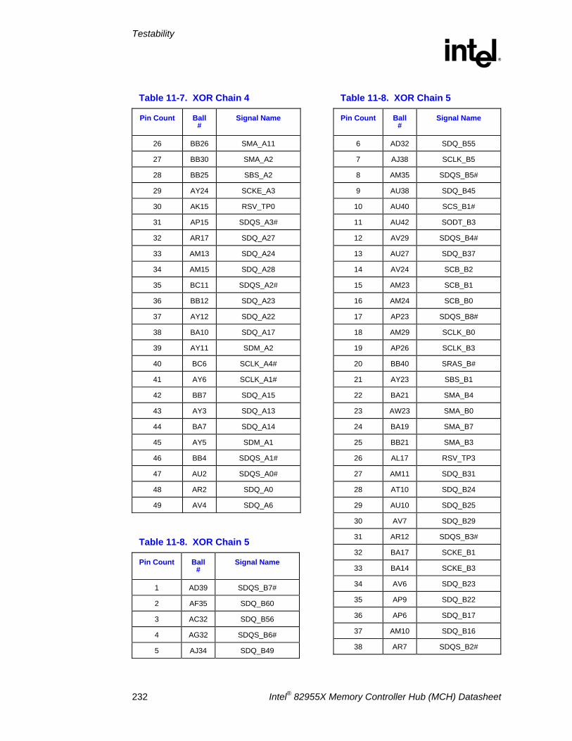
Testability
R
232 Intel® 82955X Memory Controller Hub (MCH) Datasheet
Table 11-7. XOR Chain 4
Pin Count Ball #
Signal Name
26 BB26 SMA_A11
27 BB30 SMA_A2
28 BB25 SBS_A2
29 AY24 SCKE_A3
30 AK15 RSV_TP0
31 AP15 SDQS_A3#
32 AR17 SDQ_A27
33 AM13 SDQ_A24
34 AM15 SDQ_A28
35 BC11 SDQS_A2#
36 BB12 SDQ_A23
37 AY12 SDQ_A22
38 BA10 SDQ_A17
39 AY11 SDM_A2
40 BC6 SCLK_A4#
41 AY6 SCLK_A1#
42 BB7 SDQ_A15
43 AY3 SDQ_A13
44 BA7 SDQ_A14
45 AY5 SDM_A1
46 BB4 SDQS_A1#
47 AU2 SDQS_A0#
48 AR2 SDQ_A0
49 AV4 SDQ_A6
Table 11-8. XOR Chain 5
Pin Count Ball #
Signal Name
1 AD39 SDQS_B7#
2 AF35 SDQ_B60
3 AC32 SDQ_B56
4 AG32 SDQS_B6#
5 AJ34 SDQ_B49
Table 11-8. XOR Chain 5
Pin Count Ball #
Signal Name
6 AD32 SDQ_B55
7 AJ38 SCLK_B5
8 AM35 SDQS_B5#
9 AU38 SDQ_B45
10 AU40 SCS_B1#
11 AU42 SODT_B3
12 AV29 SDQS_B4#
13 AU27 SDQ_B37
14 AV24 SCB_B2
15 AM23 SCB_B1
16 AM24 SCB_B0
17 AP23 SDQS_B8#
18 AM29 SCLK_B0
19 AP26 SCLK_B3
20 BB40 SRAS_B#
21 AY23 SBS_B1
22 BA21 SMA_B4
23 AW23 SMA_B0
24 BA19 SMA_B7
25 BB21 SMA_B3
26 AL17 RSV_TP3
27 AM11 SDQ_B31
28 AT10 SDQ_B24
29 AU10 SDQ_B25
30 AV7 SDQ_B29
31 AR12 SDQS_B3#
32 BA17 SCKE_B1
33 BA14 SCKE_B3
34 AV6 SDQ_B23
35 AP9 SDQ_B22
36 AP6 SDQ_B17
37 AM10 SDQ_B16
38 AR7 SDQS_B2#
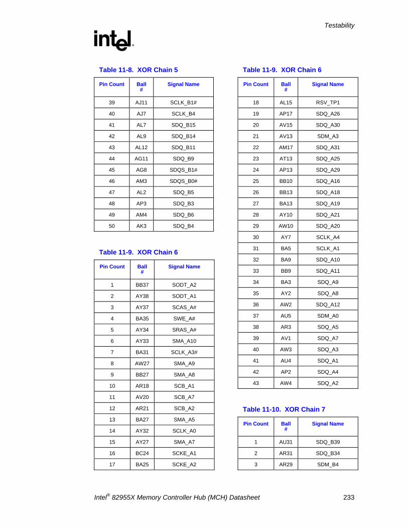
Testability
R
Intel® 82955X Memory Controller Hub (MCH) Datasheet 233
Table 11-8. XOR Chain 5
Pin Count Ball #
Signal Name
39 AJ11 SCLK_B1#
40 AJ7 SCLK_B4
41 AL7 SDQ_B15
42 AL9 SDQ_B14
43 AL12 SDQ_B11
44 AG11 SDQ_B9
45 AG8 SDQS_B1#
46 AM3 SDQS_B0#
47 AL2 SDQ_B5
48 AP3 SDQ_B3
49 AM4 SDQ_B6
50 AK3 SDQ_B4
Table 11-9. XOR Chain 6
Pin Count Ball #
Signal Name
1 BB37 SODT_A2
2 AY38 SODT_A1
3 AY37 SCAS_A#
4 BA35 SWE_A#
5 AY34 SRAS_A#
6 AY33 SMA_A10
7 BA31 SCLK_A3#
8 AW27 SMA_A9
9 BB27 SMA_A8
10 AR18 SCB_A1
11 AV20 SCB_A7
12 AR21 SCB_A2
13 BA27 SMA_A5
14 AY32 SCLK_A0
15 AY27 SMA_A7
16 BC24 SCKE_A1
17 BA25 SCKE_A2
Table 11-9. XOR Chain 6
Pin Count Ball #
Signal Name
18 AL15 RSV_TP1
19 AP17 SDQ_A26
20 AV15 SDQ_A30
21 AV13 SDM_A3
22 AM17 SDQ_A31
23 AT13 SDQ_A25
24 AP13 SDQ_A29
25 BB10 SDQ_A16
26 BB13 SDQ_A18
27 BA13 SDQ_A19
28 AY10 SDQ_A21
29 AW10 SDQ_A20
30 AY7 SCLK_A4
31 BA5 SCLK_A1
32 BA9 SDQ_A10
33 BB9 SDQ_A11
34 BA3 SDQ_A9
35 AY2 SDQ_A8
36 AW2 SDQ_A12
37 AU5 SDM_A0
38 AR3 SDQ_A5
39 AV1 SDQ_A7
40 AW3 SDQ_A3
41 AU4 SDQ_A1
42 AP2 SDQ_A4
43 AW4 SDQ_A2
Table 11-10. XOR Chain 7
Pin Count Ball #
Signal Name
1 AU31 SDQ_B39
2 AR31 SDQ_B34
3 AR29 SDM_B4
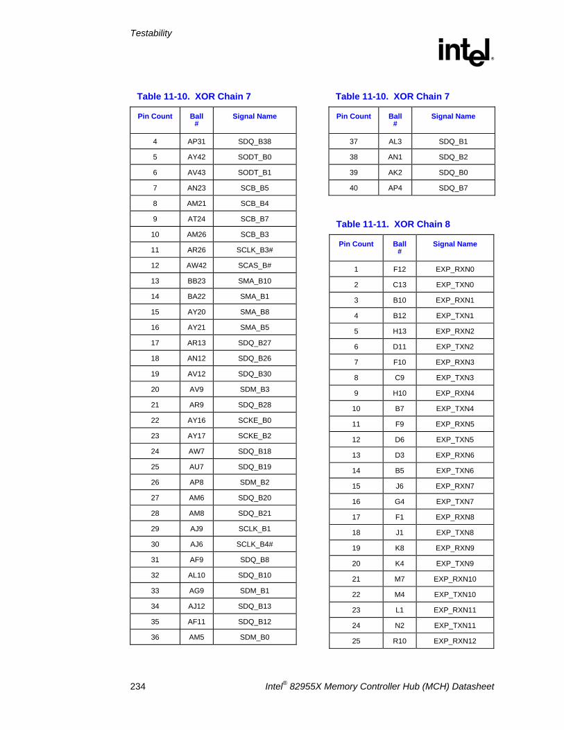
Testability
R
234 Intel® 82955X Memory Controller Hub (MCH) Datasheet
Table 11-10. XOR Chain 7
Pin Count Ball #
Signal Name
4 AP31 SDQ_B38
5 AY42 SODT_B0
6 AV43 SODT_B1
7 AN23 SCB_B5
8 AM21 SCB_B4
9 AT24 SCB_B7
10 AM26 SCB_B3
11 AR26 SCLK_B3#
12 AW42 SCAS_B#
13 BB23 SMA_B10
14 BA22 SMA_B1
15 AY20 SMA_B8
16 AY21 SMA_B5
17 AR13 SDQ_B27
18 AN12 SDQ_B26
19 AV12 SDQ_B30
20 AV9 SDM_B3
21 AR9 SDQ_B28
22 AY16 SCKE_B0
23 AY17 SCKE_B2
24 AW7 SDQ_B18
25 AU7 SDQ_B19
26 AP8 SDM_B2
27 AM6 SDQ_B20
28 AM8 SDQ_B21
29 AJ9 SCLK_B1
30 AJ6 SCLK_B4#
31 AF9 SDQ_B8
32 AL10 SDQ_B10
33 AG9 SDM_B1
34 AJ12 SDQ_B13
35 AF11 SDQ_B12
36 AM5 SDM_B0
Table 11-10. XOR Chain 7
Pin Count Ball #
Signal Name
37 AL3 SDQ_B1
38 AN1 SDQ_B2
39 AK2 SDQ_B0
40 AP4 SDQ_B7
Table 11-11. XOR Chain 8
Pin Count Ball #
Signal Name
1 F12 EXP_RXN0
2 C13 EXP_TXN0
3 B10 EXP_RXN1
4 B12 EXP_TXN1
5 H13 EXP_RXN2
6 D11 EXP_TXN2
7 F10 EXP_RXN3
8 C9 EXP_TXN3
9 H10 EXP_RXN4
10 B7 EXP_TXN4
11 F9 EXP_RXN5
12 D6 EXP_TXN5
13 D3 EXP_RXN6
14 B5 EXP_TXN6
15 J6 EXP_RXN7
16 G4 EXP_TXN7
17 F1 EXP_RXN8
18 J1 EXP_TXN8
19 K8 EXP_RXN9
20 K4 EXP_TXN9
21 M7 EXP_RXN10
22 M4 EXP_TXN10
23 L1 EXP_RXN11
24 N2 EXP_TXN11
25 R10 EXP_RXN12
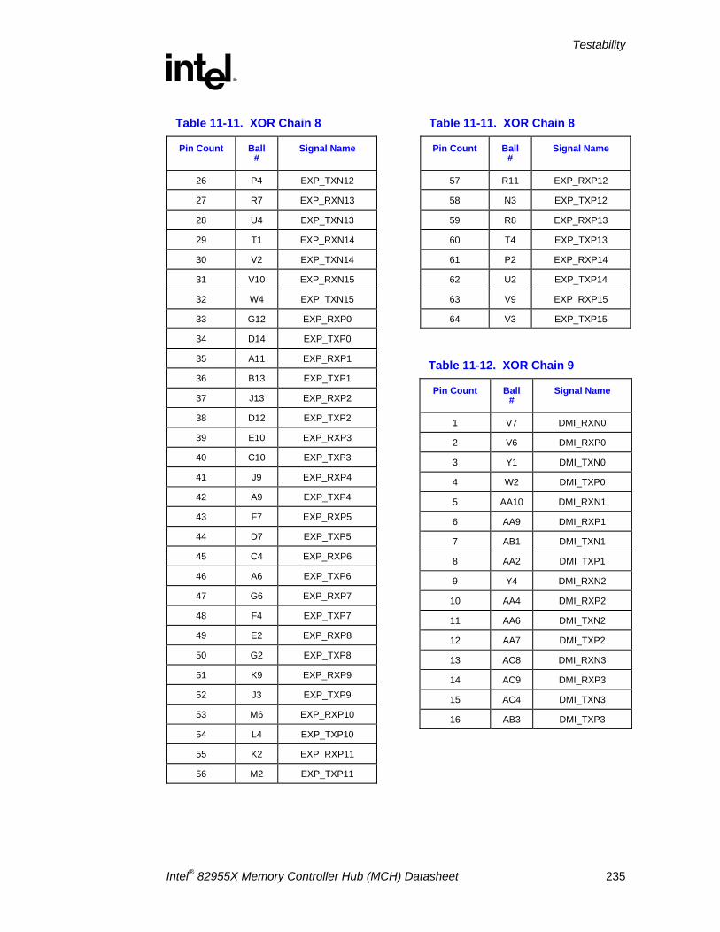
Testability
R
Intel® 82955X Memory Controller Hub (MCH) Datasheet 235
Table 11-11. XOR Chain 8
Pin Count Ball #
Signal Name
26 P4 EXP_TXN12
27 R7 EXP_RXN13
28 U4 EXP_TXN13
29 T1 EXP_RXN14
30 V2 EXP_TXN14
31 V10 EXP_RXN15
32 W4 EXP_TXN15
33 G12 EXP_RXP0
34 D14 EXP_TXP0
35 A11 EXP_RXP1
36 B13 EXP_TXP1
37 J13 EXP_RXP2
38 D12 EXP_TXP2
39 E10 EXP_RXP3
40 C10 EXP_TXP3
41 J9 EXP_RXP4
42 A9 EXP_TXP4
43 F7 EXP_RXP5
44 D7 EXP_TXP5
45 C4 EXP_RXP6
46 A6 EXP_TXP6
47 G6 EXP_RXP7
48 F4 EXP_TXP7
49 E2 EXP_RXP8
50 G2 EXP_TXP8
51 K9 EXP_RXP9
52 J3 EXP_TXP9
53 M6 EXP_RXP10
54 L4 EXP_TXP10
55 K2 EXP_RXP11
56 M2 EXP_TXP11
Table 11-11. XOR Chain 8
Pin Count Ball #
Signal Name
57 R11 EXP_RXP12
58 N3 EXP_TXP12
59 R8 EXP_RXP13
60 T4 EXP_TXP13
61 P2 EXP_RXP14
62 U2 EXP_TXP14
63 V9 EXP_RXP15
64 V3 EXP_TXP15
Table 11-12. XOR Chain 9
Pin Count Ball #
Signal Name
1 V7 DMI_RXN0
2 V6 DMI_RXP0
3 Y1 DMI_TXN0
4 W2 DMI_TXP0
5 AA10 DMI_RXN1
6 AA9 DMI_RXP1
7 AB1 DMI_TXN1
8 AA2 DMI_TXP1
9 Y4 DMI_RXN2
10 AA4 DMI_RXP2
11 AA6 DMI_TXN2
12 AA7 DMI_TXP2
13 AC8 DMI_RXN3
14 AC9 DMI_RXP3
15 AC4 DMI_TXN3
16 AB3 DMI_TXP3
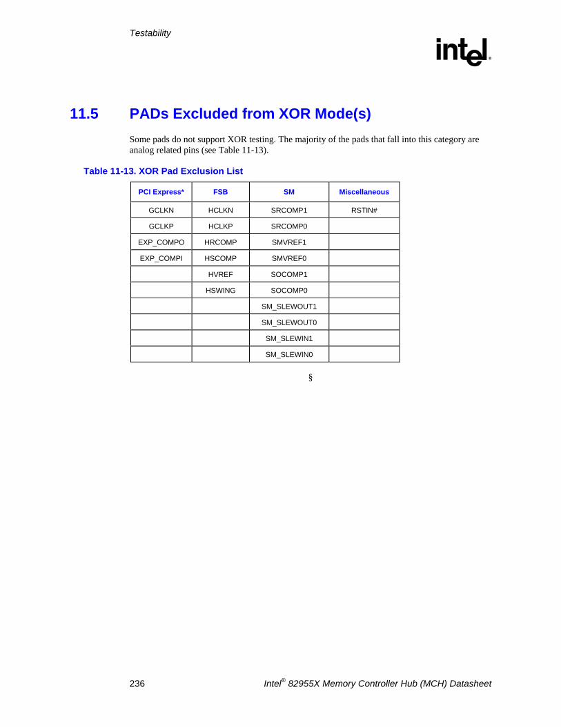
Testability
R
236 Intel® 82955X Memory Controller Hub (MCH) Datasheet
11.5 PADs Excluded from XOR Mode(s) Some pads do not support XOR testing. The majority of the pads that fall into this category are analog related pins (see Table 11-13).
Table 11-13. XOR Pad Exclusion List
PCI Express* FSB SM Miscellaneous
GCLKN HCLKN SRCOMP1 RSTIN#
GCLKP HCLKP SRCOMP0
EXP_COMPO HRCOMP SMVREF1
EXP_COMPI HSCOMP SMVREF0
HVREF SOCOMP1
HSWING SOCOMP0
SM_SLEWOUT1
SM_SLEWOUT0
SM_SLEWIN1
SM_SLEWIN0
§


![Untitled-1 []CHIPSET H310 intel CORE i3 9th Gen intel CHIPSET 8360 inside- nVlDIA. intel CORE i3 9th Gen B450 nvlDlA. EXPRESS AMDa RYZEN CHIPSET Z390 RTX nvmG>](https://static.documents.pub/doc/80x56/5e59c307f785412c3122cc95/untitled-1-chipset-h310-intel-core-i3-9th-gen-intel-chipset-8360-inside-nvldia.jpg)


