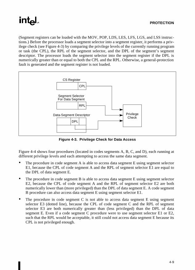
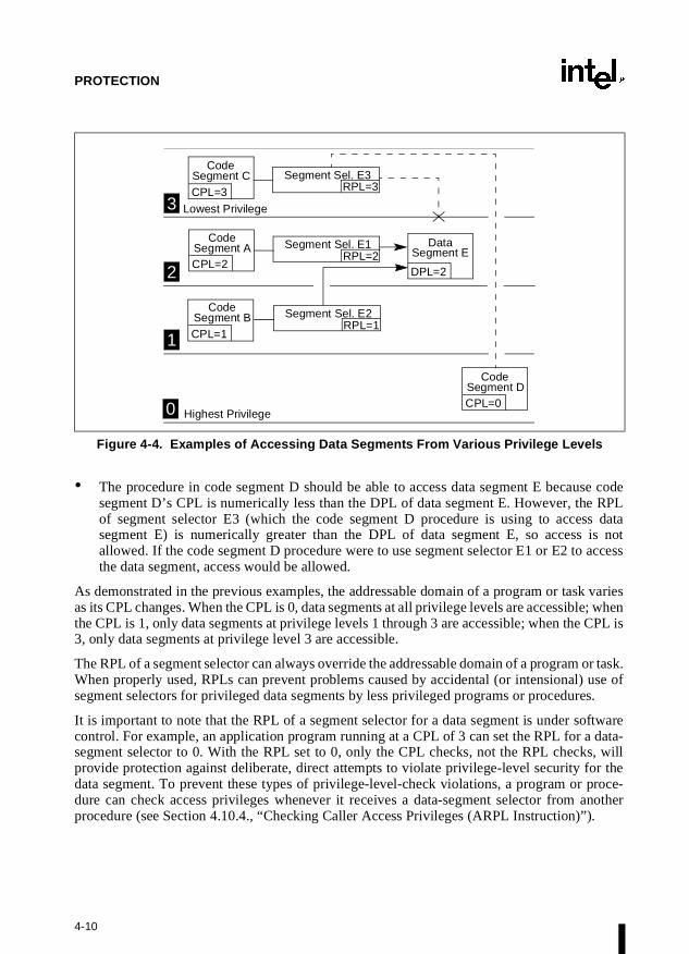
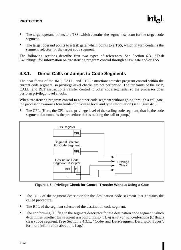
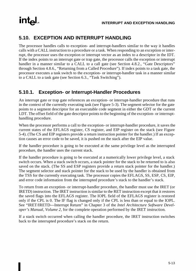
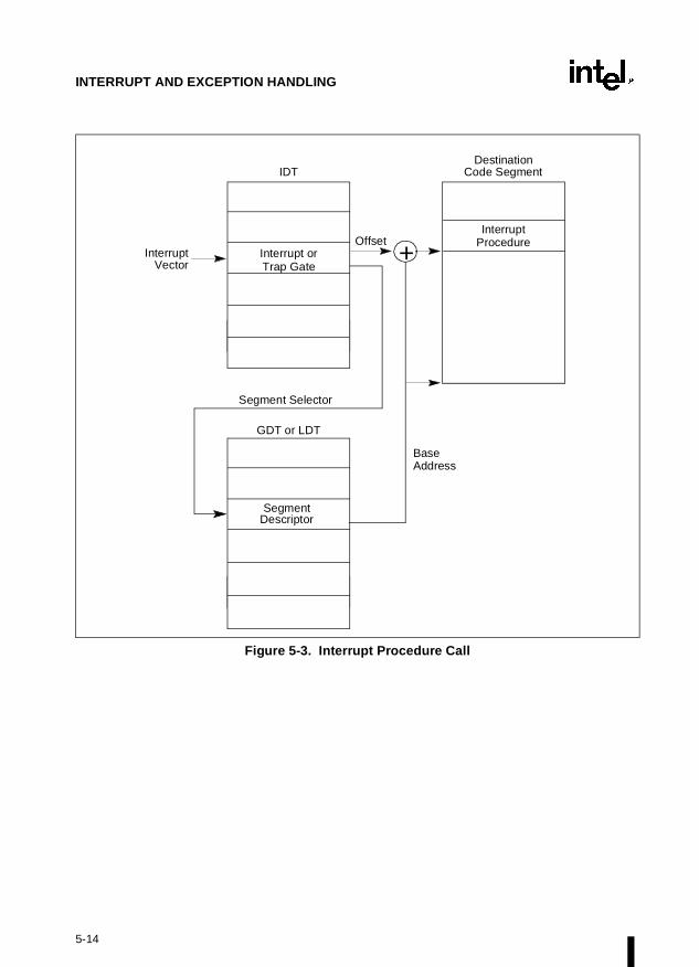
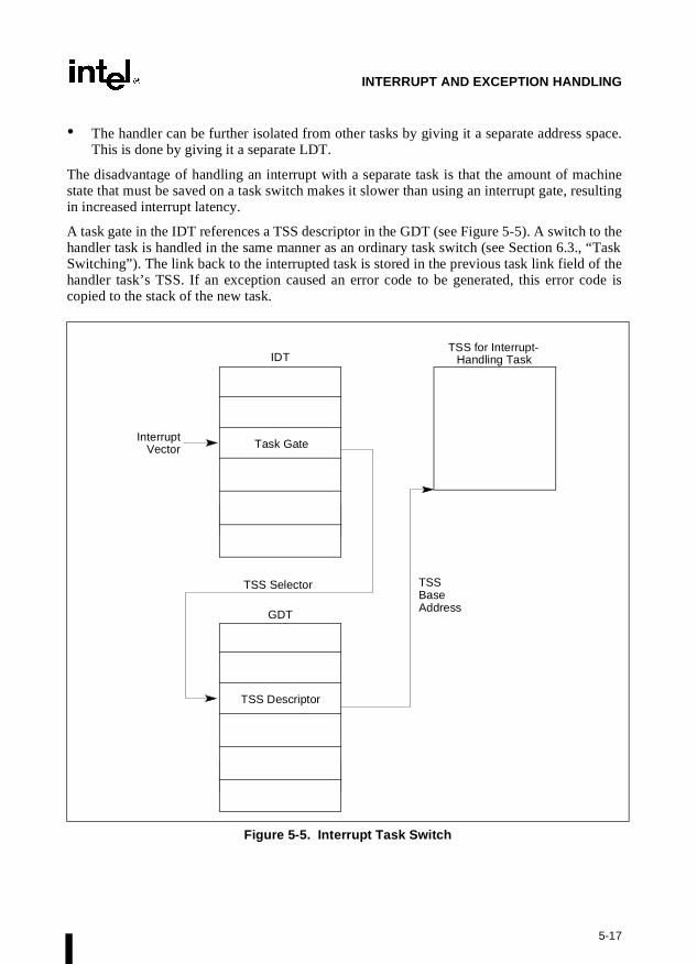
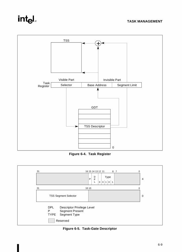
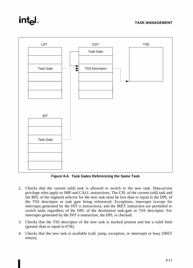
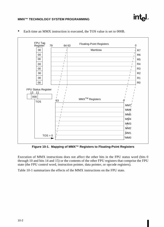
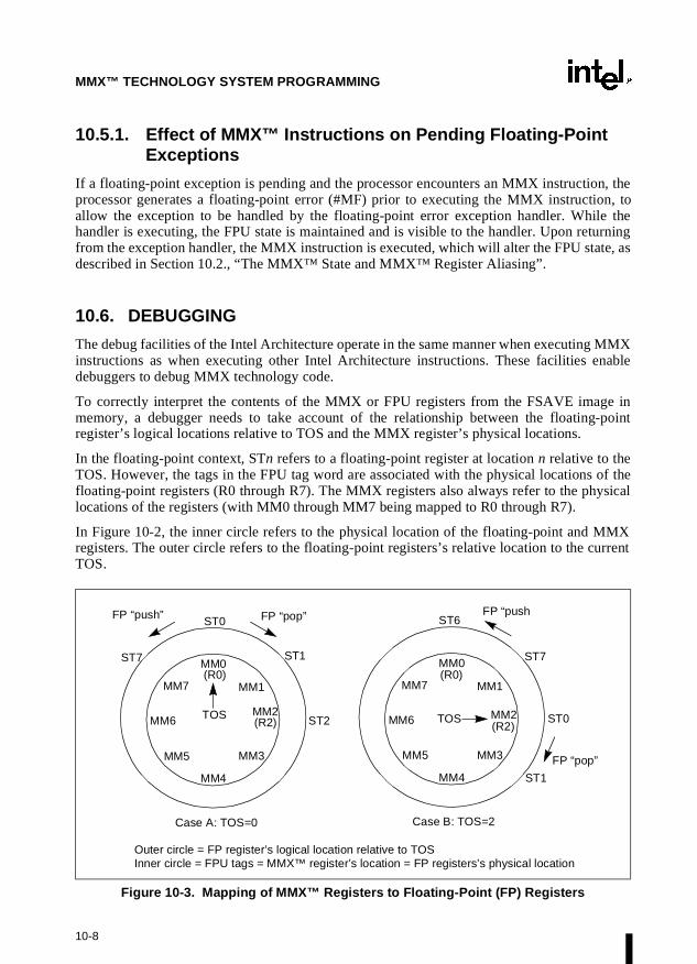
Intel Architecture Software Developer’s Manual Volume 3: System Programming Guide NOTE: The Intel Architecture Developer’s Manual consists of three books: Basic Architecture, Order Number 243190; Instruction Set Reference Manual, Order Number 243191; and the System Programming Guide, Order Number 243192. Please refer to all three volumes when evaluating your design needs. 1997
Transcript
Intel ArchitectureSoftware Developer’s
Manual
Volume 3:System Programming Guide
NOTE: The Intel Architecture Developer’s Manual consists of threebooks: Basic Architecture, Order Number 243190; Instruction Set
Reference Manual, Order Number 243191; and the System ProgrammingGuide, Order Number 243192.
Please refer to all three volumes when evaluating your design needs.
1997
Information in this document is provided in connection with Intel products. No license, express or implied, by estoppelor otherwise, to any intellectual property rights is granted by this document. Except as provided in Intel's Terms andConditions of Sale for such products, Intel assumes no liability whatsoever, and Intel disclaims any express or impliedwarranty, relating to sale and/or use of Intel products including liability or warranties relating to fitness for a particularpurpose, merchantability, or infringement of any patent, copyright or other intellectual property right. Intel products arenot intended for use in medical, life saving, or life sustaining applications.
Intel may make changes to specifications and product descriptions at any time, without notice.
Designers must not rely on the absence or characteristics of any features or instructions marked "reserved" or"undefined." Intel reserves these for future definition and shall have no responsibility whatsoever for conflicts orincompatibilities arising from future changes to them.
Intel’s Intel Architecture processors (e.g., Pentium® and Pentium Pro processors) may contain design defects orerrors known as errata which may cause the product to deviate from published specifications. Current characterizederrata are available on request.
Contact your local Intel sales office or your distributor to obtain the latest specifications and before placing yourproduct order.Copies of documents which have an ordering number and are referenced in this document, or other Intelliterature, may be obtained from:
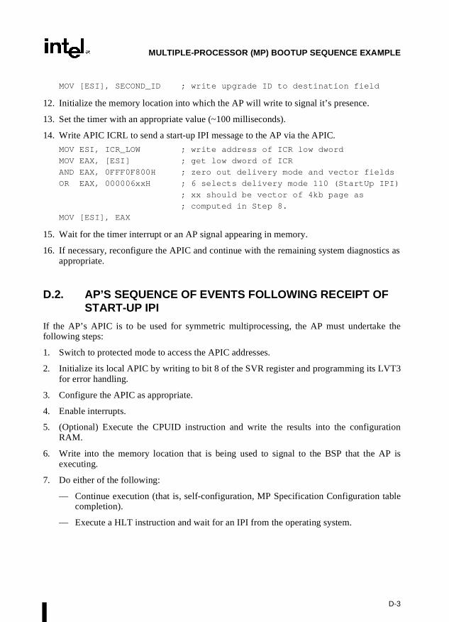
Intel CorporationP.O. Box 7641Mt. Prospect IL 60056-7641
or call 1-800-879-4683or visit Intel’s website at http://www.intel.com
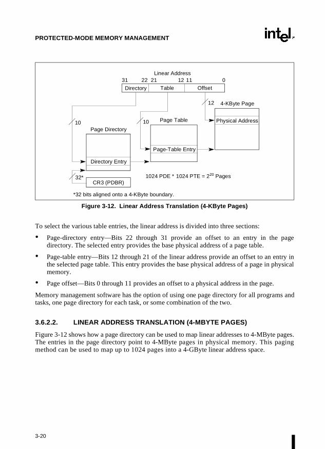
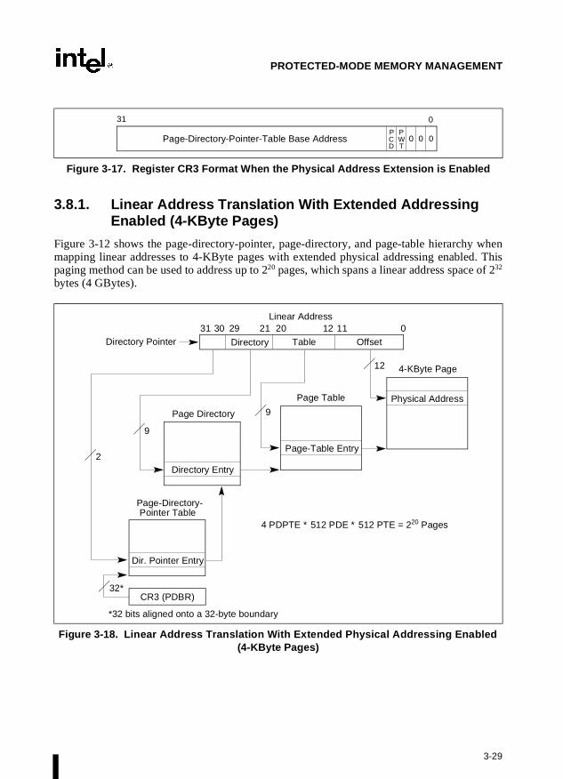
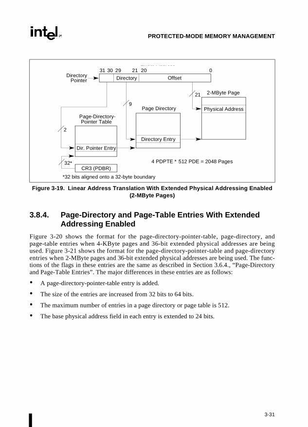
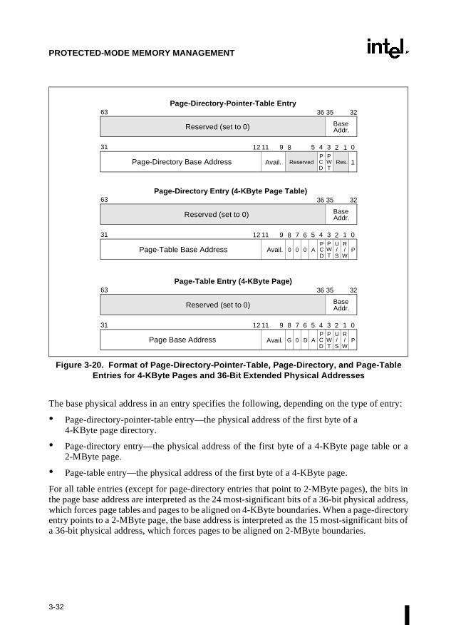
Entries for 4-KByte Pages and 36-Bit Extended Physical Addresses . . . . . .3-32Figure 3-21. Format of Page-Directory-Pointer-Table and Page-Directory Entries for
2-MByte Pages and 36-Bit Extended Physical Addresses . . . . . . . . . . . . . . .3-33Figure 3-22. Memory Management Convention That Assigns a Page Table to Each
The Intel Architecture Software Developer’s Manual, Volume 3: System Programming Guide(Order Number 243192), is part of a three-volume set that describes the architecture andprogramming environment of all Intel Architecture processors. The other two volumes in thisset are:
• The Intel Architecture Software Developer’s Manual, Volume 2: Instruction Set Reference(Order Number 243191).
The Intel Architecture Software Developer’s Manual, Volume 1, describes the basic architectureand programming environment of an Intel Architecture processor; the Intel Architecture Soft-ware Developer’s Manual, Volume 2, describes the instruction set of the processor and theopcode structure. These two volumes are aimed at application programmers who are writingprograms to run under existing operating systems or executives. The Intel Architecture SoftwareDeveloper’s Manual, Volume 3, describes the operating-system support environment of an IntelArchitecture processor, including memory management, protection, task management, interruptand exception handling, and system management mode. It also provides Intel Architectureprocessor compatibility information. This volume is aimed at operating-system and BIOSdesigners and programmers.
1.1. P6 FAMILY PROCESSOR TERMINOLOGY
This manual includes information pertaining primarily to the 32-bit Intel Architecture proces-sors, which include the Intel386™, Intel486™, and Pentium® processors, and the P6 familyprocessors. The P6 family processors are those Intel Architecture processors based on the P6family microarchitecture. This family includes the Pentium Pro and Pentium II processors andany future processor based on the P6 family microarchitecture.
1.2. OVERVIEW OF THE INTEL ARCHITECTURE SOFTWARE DEVELOPER’S MANUAL, VOLUME 3 : SYSTEM PROGRAMMING GUIDE
The contents of this manual are as follows:
Chapter 1 — About This Manual. Gives an overview of all three volumes of the Intel Archi-tecture Software Developer’s Manual. It also describes the notational conventions in thesemanuals and lists related Intel manuals and documentation of interest to programmers and hard-ware designers.
1-2
ABOUT THIS MANUAL
Chapter 2 — System Architecture Overview. Describes the modes of operation of an IntelArchitecture processor and the mechanisms provided in the Intel Architecture to support oper-ating systems and executives, including the system-oriented registers and data structures and thesystem-oriented instructions. The steps necessary for switching between real-address andprotected modes are also identified.
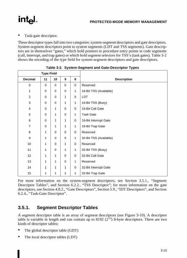
Chapter 3 — Protected-Mode Memory Management. Describes the data structures, regis-ters, and instructions that support segmentation and paging and explains how they can be usedto implement a “flat” (unsegmented) memory model or a segmented memory model.
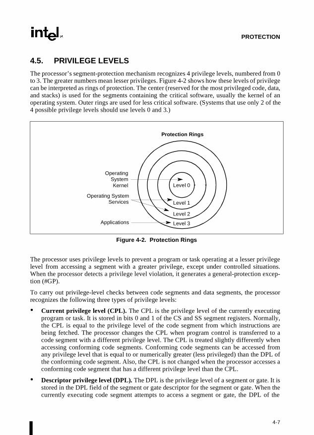
Chapter 4 — Protection. Describes the support for page and segment protection provided inthe Intel Architecture. This chapter also explains the implementation of privilege rules, stackswitching, pointer validation, user and supervisor modes.
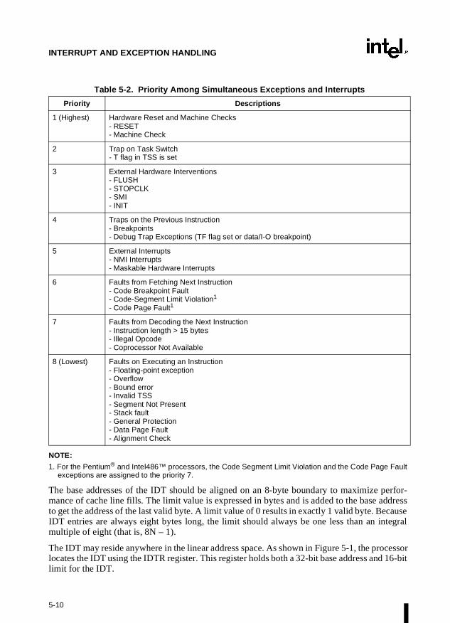
Chapter 5 — Interrupt and Exception Handling. Describes the basic interrupt mechanismsdefined in the Intel Architecture, shows how interrupts and exceptions relate to protection, anddescribes how the architecture handles each exception type. Reference information for eachIntel Architecture exception is given at the end of this chapter.
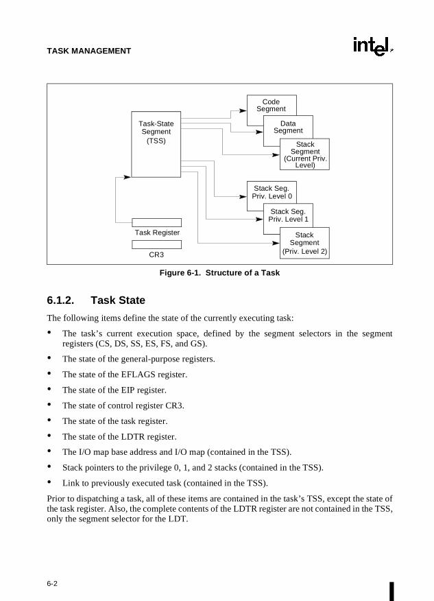
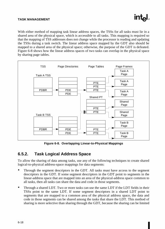
Chapter 6 — Task Management. Describes the mechanisms the Intel Architecture provides tosupport multitasking and inter-task protection.
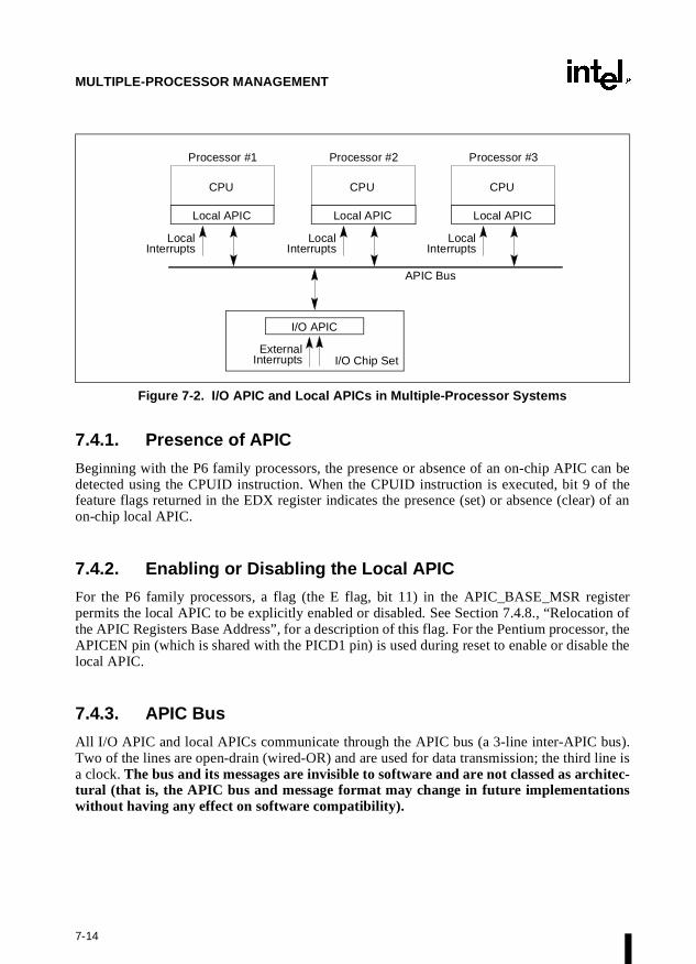
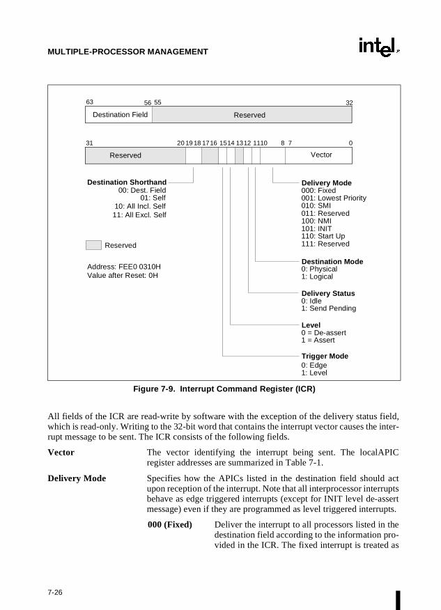
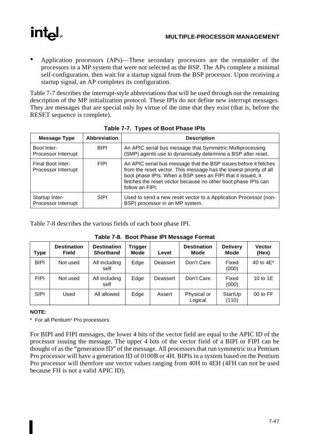
Chapter 7 — Multiple-Processor Management. Describes the instructions and flags thatsupport multiple processors with shared memory, memory ordering, and the advanced program-mable interrupt controller (APIC).
Chapter 8 — Processor Management and Initialization. Defines the state of an Intel Archi-tecture processor and its floating-point unit after reset initialization. This chapter also explainshow to set up an Intel Architecture processor for real-address mode operation and protected-mode operation, and how to switch between modes.
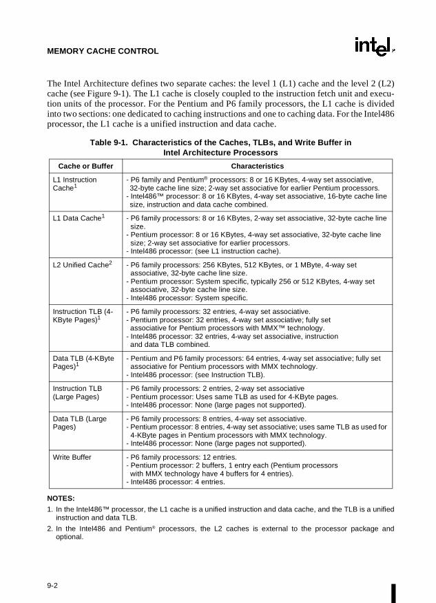
Chapter 9 — Memory Cache Control. Describes the general concept of caching and thecaching mechanisms supported by the Intel Architecture. This chapter also describes thememory type range registers (MTRRs) and how they can be used to map memory types of phys-ical memory. MTRRs were introduced into the Intel Architecture with the Pentium Proprocessor.
Chapter 10 — MMX™ Technology System Programming. Describes those aspects of theIntel MMX™ technology that must be handled and considered at the system programming level,including task switching, exception handling, and compatibility with existing system environ-ments. The MMX technology was introduced into the Intel Architecture with the Pentiumprocessor.
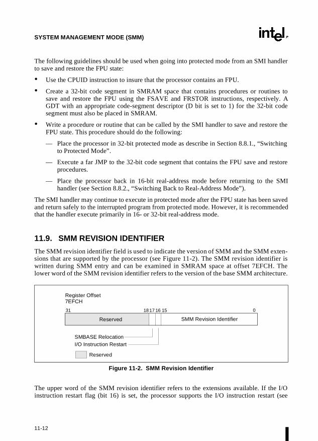
Chapter 11 — System Management Mode (SMM). Describes the Intel Architecture’s systemmanagement mode (SMM), which can be used to implement power management functions.
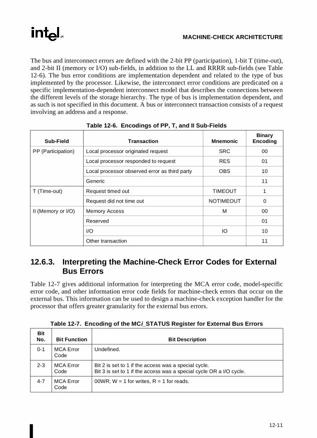
Chapter 12 — Machine-Check Architecture. Describes the machine-check architecture,which was introduced into the Intel Architecture with the Pentium processor.
Chapter 13 — Code Optimization. Discusses general optimization techniques for program-ming an Intel Architecture processor.
1-3
ABOUT THIS MANUAL
Chapter 14 — Debugging and Performance Monitoring. Describes the debugging registersand other debug mechanism provided in the Intel Architecture. This chapter also describes thetime-stamp counter and the performance-monitoring counters.
Chapter 15 — 8086 Emulation. Describes the real-address and virtual-8086 modes of the IntelArchitecture.
Chapter 16 — Mixing 16-Bit and 32-Bit Code. Describes how to mix 16-bit and 32-bit codemodules within the same program or task.
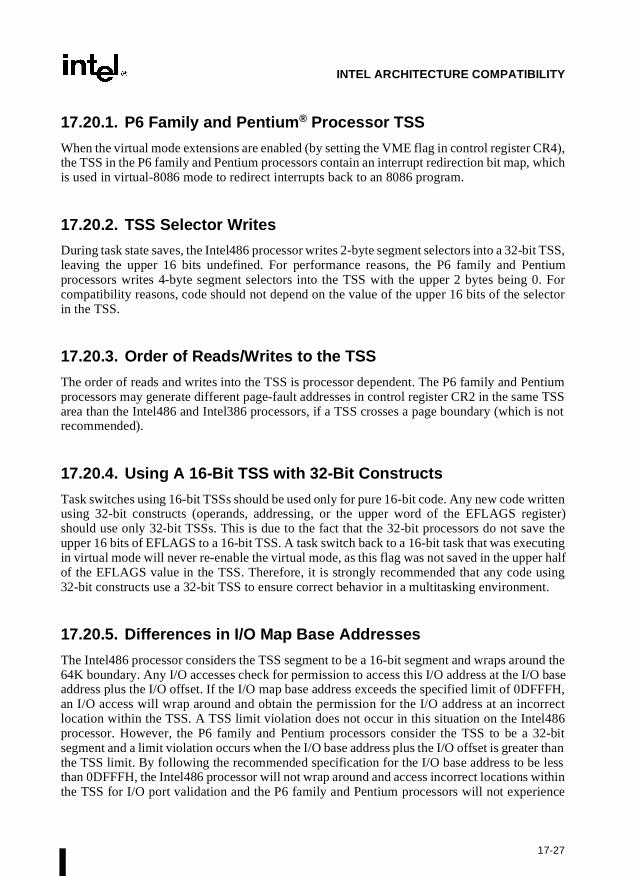
Chapter 17 — Intel Architecture Compatibility. Describes the programming differencesbetween the Intel 286, Intel386, Intel486, Pentium, and P6 family processors. The differencesamong the 32-bit Intel Architecture processors (the Intel386, Intel486, Pentium, and P6 familyprocessors) are described throughout the three volumes of the Intel Architecture SoftwareDeveloper’s Manual, as relevant to particular features of the architecture. This chapter providesa collection of all the relevant compatibility information for all Intel Architecture processors andalso describes the basic differences with respect to the 16-bit Intel Architecture processors (theIntel 8086 and Intel 286 processors).
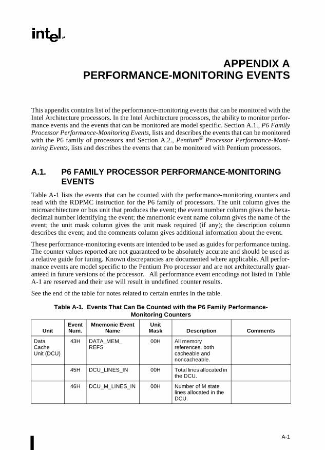
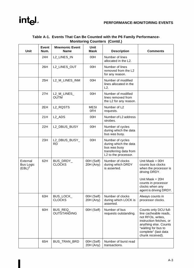
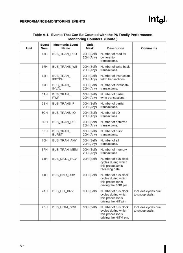
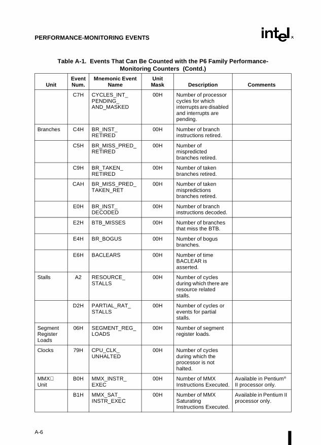
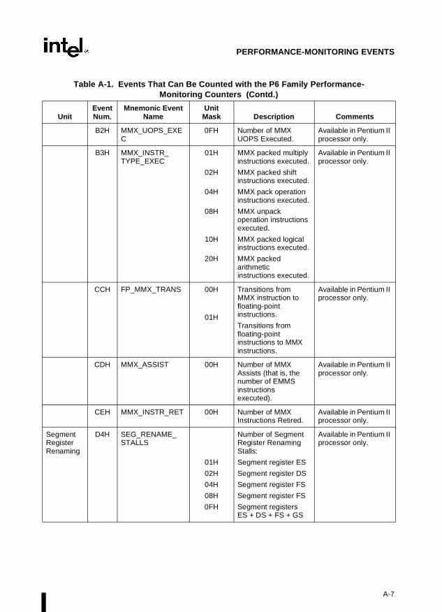
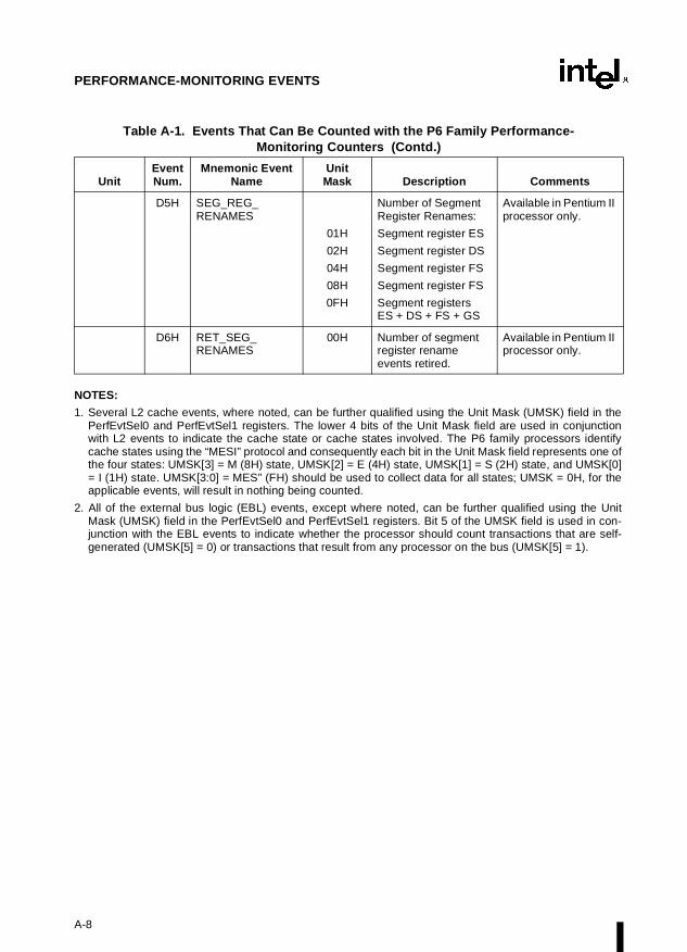
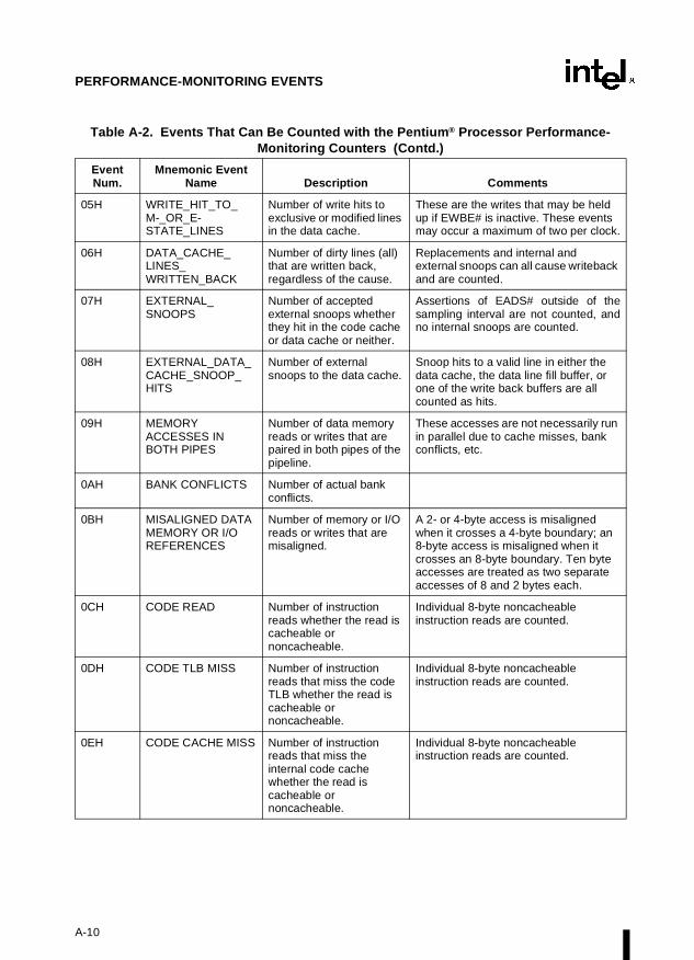
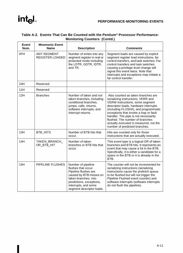
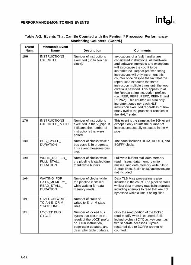
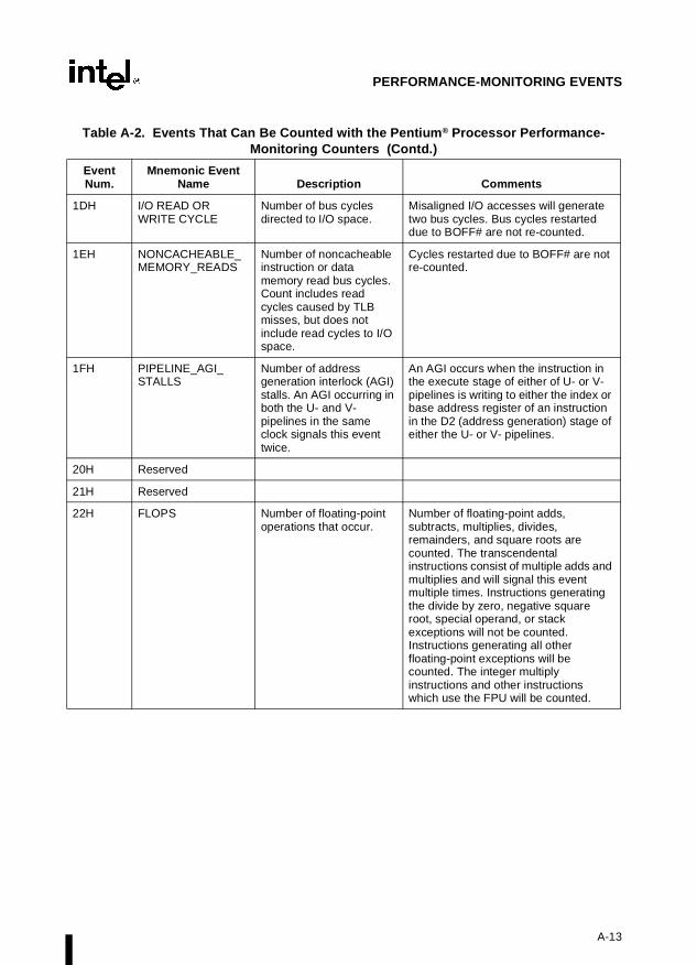
Appendix A — Performance-Monitoring Events. Lists the events that can be counted withthe performance-monitoring counters and the codes used to select these events. Both Pentiumprocessor and P6 family processor events are described.
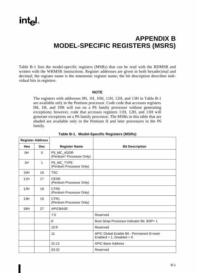
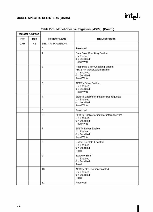
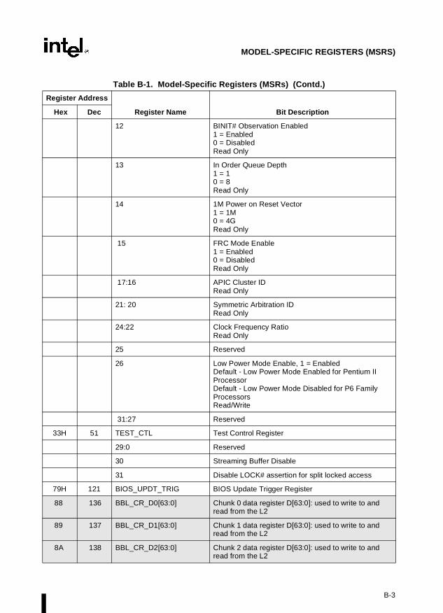
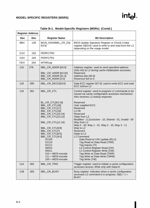
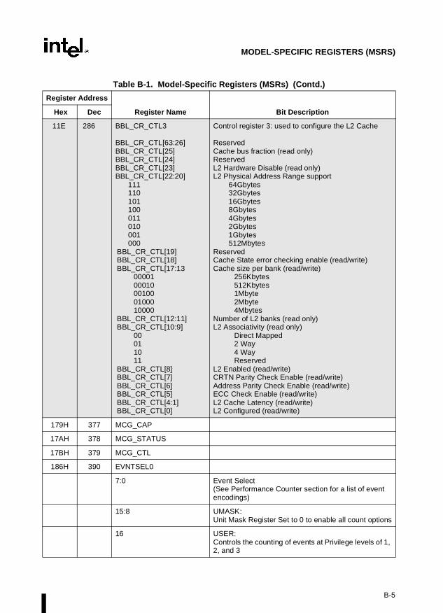
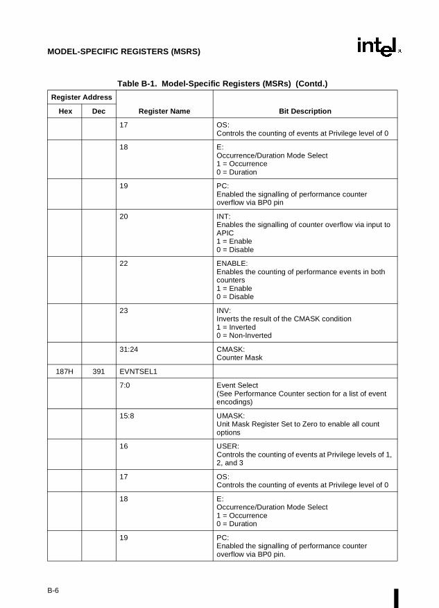
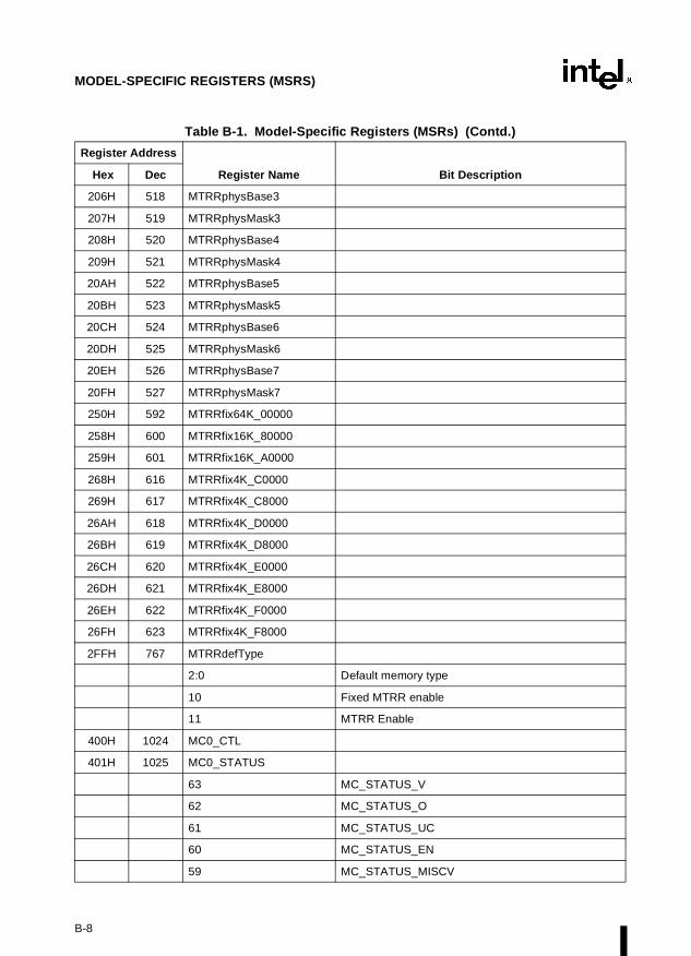
Appendix B — Model-Specific Registers (MSRs). Lists the MSRs available in the Pentiumand P6 family processors and their functions.
Appendix C — Dual-Processor (DP) Bootup Sequence Example (Specific to Pentium®
Processors). Gives an example of how to use the DP protocol to boot two Pentium processors(a primary processor and a secondary processor) in a DP system and initialize their APICs.
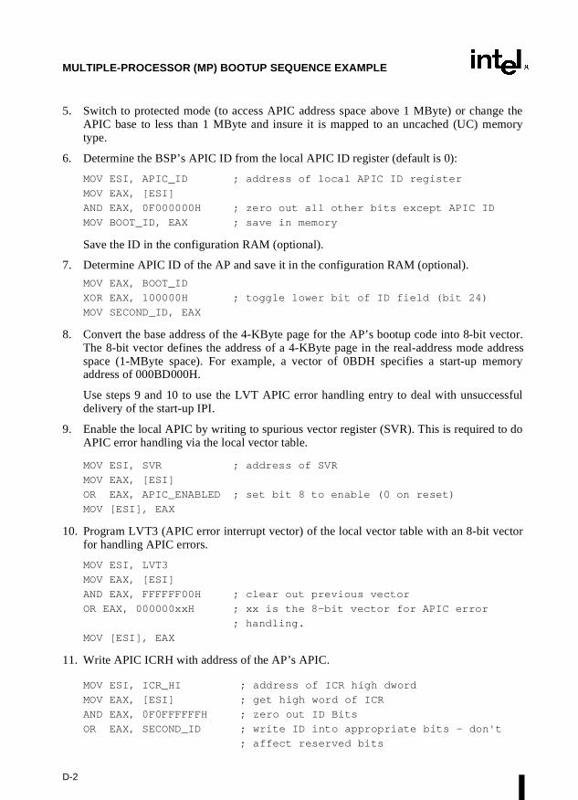
Appendix D — Multiple-Processor (MP) Bootup Sequence Example (Specific to P6 FamilyProcessors). Gives an example of how to use of the MP protocol to boot two P6 family proces-sors in a multiple-processor (MP) system and initialize their APICs.
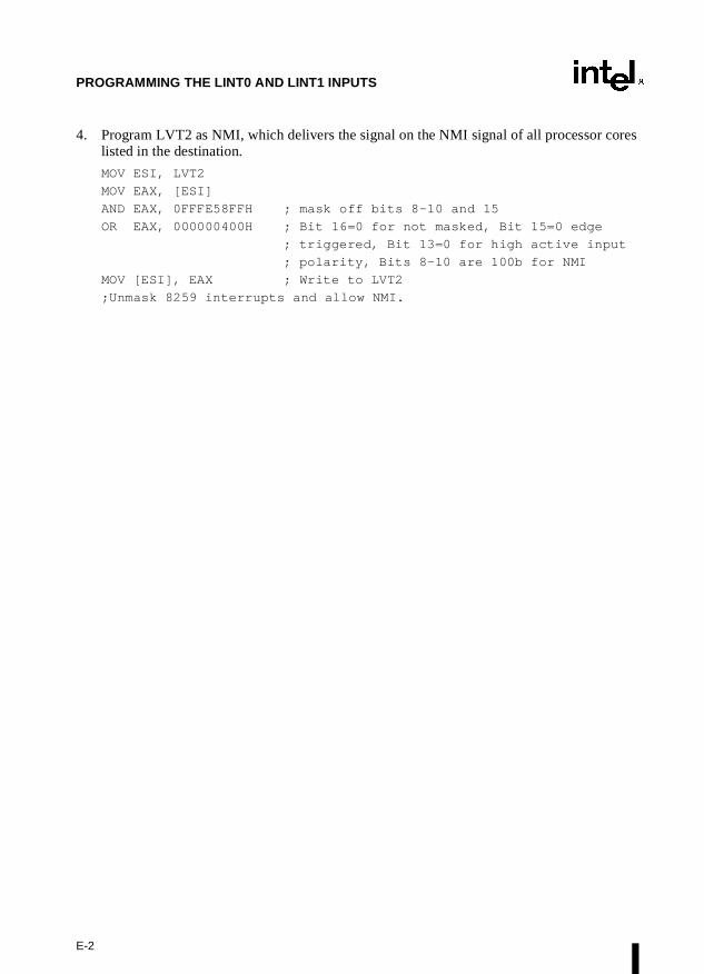
Appendix E — Programming the LINT0 and LINT1 Inputs. Gives an example of how toprogram the LINT0 and LINT1 pins for specific interrupt vectors.
1.3. OVERVIEW OF THE INTEL ARCHITECTURE SOFTWARE DEVELOPER’S MANUAL, VOLUME 1: BASIC ARCHITECTURE
The contents of the Intel Architecture Software Developer’s Manual, Volume 1 are as follows:
Chapter 1 — About This Manual. Gives an overview of all three volumes of the Intel Archi-tecture Software Developer’s Manual. It also describes the notational conventions in thesemanuals and lists related Intel manuals and documentation of interest to programmers and hard-ware designers.
1-4
ABOUT THIS MANUAL
Chapter 2 — Introduction to the Intel Architecture. Introduces the Intel Architecture and thefamilies of Intel processors that are based on this architecture. It also gives an overview of thecommon features found in these processors and brief history of the Intel Architecture.
Chapter 3 — Basic Execution Environment. Introduces the models of memory organizationand describes the register set used by applications.
Chapter 4 — Procedure Calls, Interrupts, and Exceptions. Describes the procedure stackand the mechanisms provided for making procedure calls and for servicing interrupts andexceptions.
Chapter 5 — Data Types and Addressing Modes. Describes the data types and addressingmodes recognized by the processor.
Chapter 6 — Instruction Set Summary. Gives an overview of all the Intel Architectureinstructions except those executed by the processor’s floating-point unit. The instructions arepresented in functionally related groups.
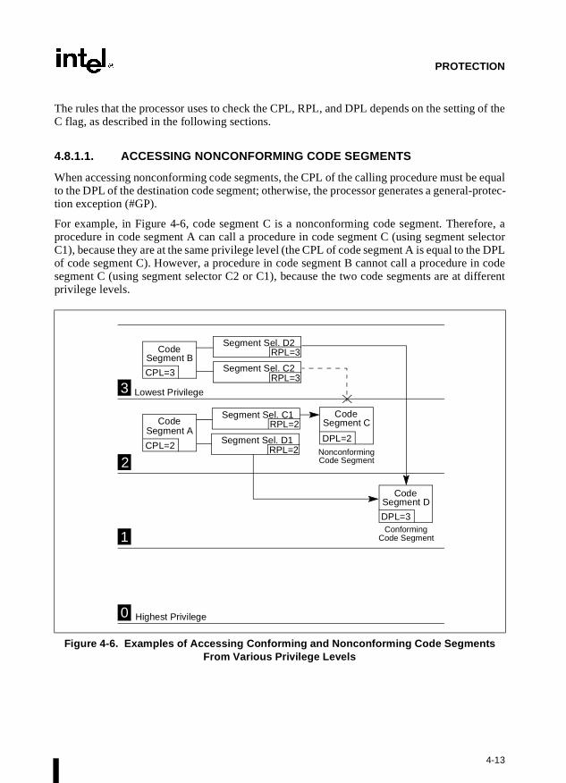
Chapter 7 — Floating-Point Unit. Describes the Intel Architecture floating-point unit,including the floating-point registers and data types; gives an overview of the floating-pointinstruction set; and describes the processor's floating-point exception conditions.
Chapter 8 — Programming with the Intel MMX™ Technology. Describes the Intel MMXtechnology, including MMX registers and data types, and gives an overview of the MMXinstruction set.
Chapter 9 — Input/Output. Describes the processor’s I/O architecture, including I/O portaddressing, the I/O instructions, and the I/O protection mechanism.
Chapter 10 — Processor Identification and Feature Determination. Describes how to deter-mine the CPU type and the features that are available in the processor.
Appendix A — EFLAGS Cross-Reference. Summaries how the Intel Architecture instruc-tions affect the flags in the EFLAGS register.
Appendix B — EFLAGS Condition Codes. Summarizes how the conditional jump, move, andbyte set on condition code instructions use the condition code flags (OF, CF, ZF, SF, and PF) inthe EFLAGS register.
Appendix C — Floating-Point Exceptions Summary. Summarizes the exceptions that can beraised by floating-point instructions.
Appendix D — Guidelines for Writing FPU Exception Handlers. Describes how to designand write MS-DOS* compatible exception-handling facilities for FPU exceptions, includingboth software and hardware requirements and assembly-language code examples. Thisappendix also describes general techniques for writing robust FPU exception handlers.
1-5
ABOUT THIS MANUAL
1.4. OVERVIEW OF THE INTEL ARCHITECTURE SOFTWARE DEVELOPER’S MANUAL, VOLUME 2: INSTRUCTION SET REFERENCE
The contents of the Intel Architecture Software Developer’s Manual, Volume 2, are as follows:
Chapter 1 — About This Manual. Gives an overview of all three volumes of the Intel Archi-tecture Software Developer’s Manual. It also describes the notational conventions in thesemanuals and lists related Intel manuals and documentation of interest to programmers and hard-ware designers.
Chapter 2 — Instruction Format. Describes the machine-level instruction format used for allIntel Architecture instructions and gives the allowable encodings of prefixes, the operand-iden-tifier byte (ModR/M byte), the addressing-mode specifier byte (SIB byte), and the displacementand immediate bytes.
Chapter 3 — Instruction Set Reference. Describes each of the Intel Architecture instructionsin detail, including an algorithmic description of operations, the effect on flags, the effect ofoperand- and address-size attributes, and the exceptions that may be generated. The instructionsare arranged in alphabetical order. The FPU and MMX instructions are included in this chapter.
Appendix A — Opcode Map. Gives an opcode map for the Intel Architecture instruction set.
Appendix B — Instruction Formats and Encodings. Gives the binary encoding of each formof each Intel Architecture instruction.
1.5. NOTATIONAL CONVENTIONS
This manual uses special notation for data-structure formats, for symbolic representation ofinstructions, and for hexadecimal numbers. A review of this notation makes the manual easierto read.
1.5.1. Bit and Byte Order
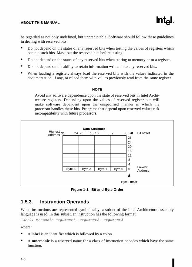
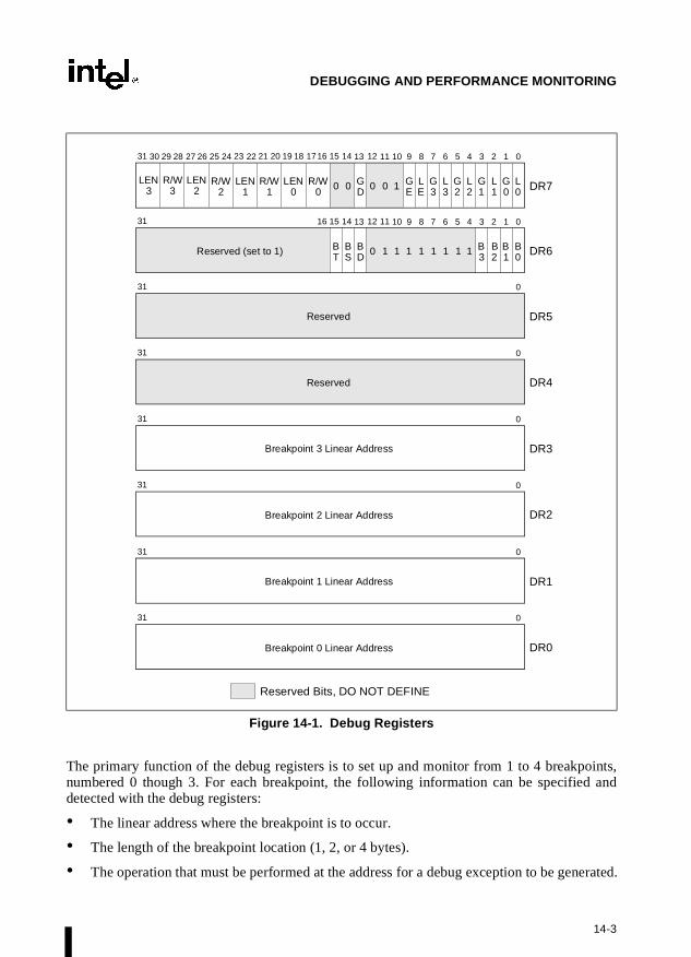
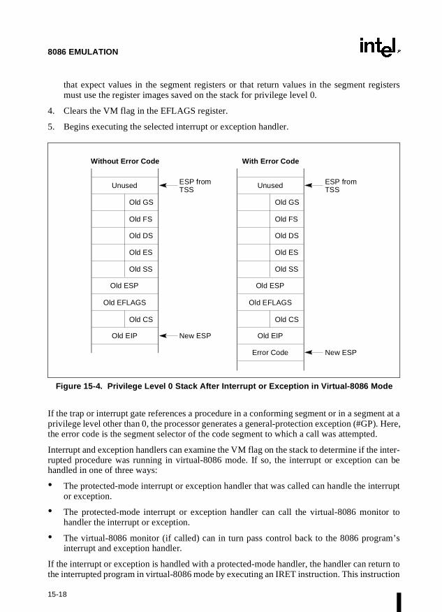
In illustrations of data structures in memory, smaller addresses appear toward the bottom of thefigure; addresses increase toward the top. Bit positions are numbered from right to left. Thenumerical value of a set bit is equal to two raised to the power of the bit position. Intel Archi-tecture processors are “little endian” machines; this means the bytes of a word are numberedstarting from the least significant byte. Figure 1-1 illustrates these conventions.
1.5.2. Reserved Bits and Software Compatibility
In many register and memory layout descriptions, certain bits are marked as reserved. Whenbits are marked as reserved, it is essential for compatibility with future processors that softwaretreat these bits as having a future, though unknown, effect. The behavior of reserved bits should
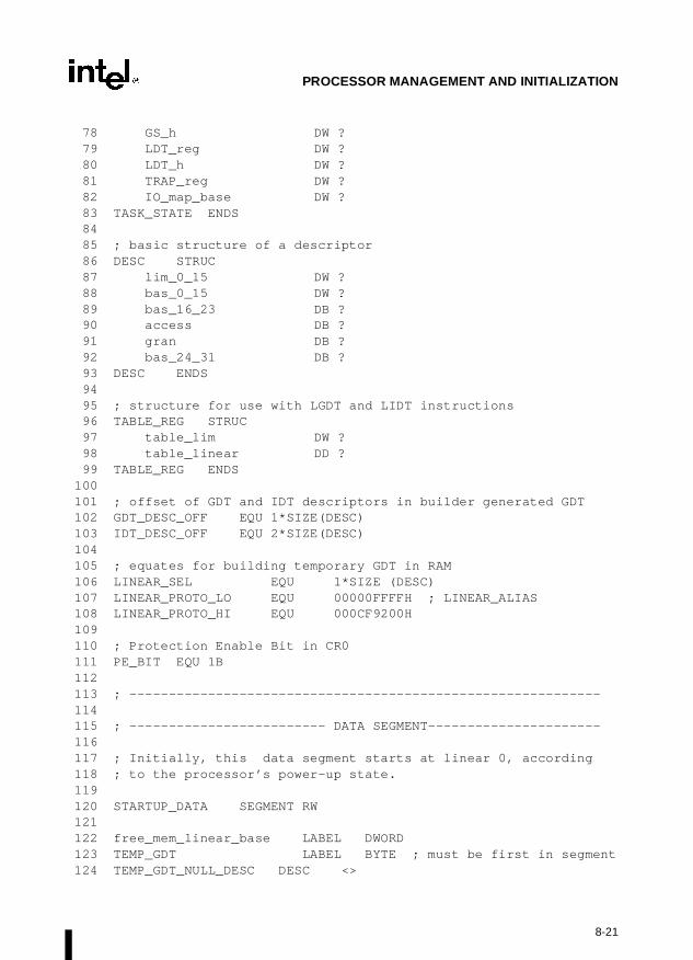
1-6
ABOUT THIS MANUAL
be regarded as not only undefined, but unpredictable. Software should follow these guidelinesin dealing with reserved bits:
• Do not depend on the states of any reserved bits when testing the values of registers whichcontain such bits. Mask out the reserved bits before testing.
• Do not depend on the states of any reserved bits when storing to memory or to a register.
• Do not depend on the ability to retain information written into any reserved bits.
• When loading a register, always load the reserved bits with the values indicated in thedocumentation, if any, or reload them with values previously read from the same register.
NOTE
Avoid any software dependence upon the state of reserved bits in Intel Archi-tecture registers. Depending upon the values of reserved register bits willmake software dependent upon the unspecified manner in which theprocessor handles these bits. Programs that depend upon reserved values riskincompatibility with future processors.
1.5.3. Instruction Operands
When instructions are represented symbolically, a subset of the Intel Architecture assemblylanguage is used. In this subset, an instruction has the following format:label: mnemonic argument1, argument2, argument3
where:
• A label is an identifier which is followed by a colon.
• A mnemonic is a reserved name for a class of instruction opcodes which have the samefunction.
Figure 1-1. Bit and Byte Order
Byte 3
HighestData Structure
Byte 1Byte 2 Byte 0
31 24 23 16 15 8 7 0Address
Lowest
Bit offset28
2420161284
0 Address
Byte Offset
1-7
ABOUT THIS MANUAL
• The operands argument1, argument2, and argument3 are optional. There may be fromzero to three operands, depending on the opcode. When present, they take the form ofeither literals or identifiers for data items. Operand identifiers are either reserved names ofregisters or are assumed to be assigned to data items declared in another part of theprogram (which may not be shown in the example).
When two operands are present in an arithmetic or logical instruction, the right operand is thesource and the left operand is the destination.
For example:
LOADREG: MOV EAX, SUBTOTAL
In this example LOADREG is a label, MOV is the mnemonic identifier of an opcode, EAX isthe destination operand, and SUBTOTAL is the source operand. Some assembly languages putthe source and destination in reverse order.
1.5.4. Hexadecimal and Binary Numbers
Base 16 (hexadecimal) numbers are represented by a string of hexadecimal digits followed bythe character H (for example, F82EH). A hexadecimal digit is a character from the followingset: 0, 1, 2, 3, 4, 5, 6, 7, 8, 9, A, B, C, D, E, and F.
Base 2 (binary) numbers are represented by a string of 1s and 0s, sometimes followed by thecharacter B (for example, 1010B). The “B” designation is only used in situations where confu-sion as to the type of number might arise.
1.5.5. Segmented Addressing
The processor uses byte addressing. This means memory is organized and accessed as asequence of bytes. Whether one or more bytes are being accessed, a byte address is used tolocate the byte or bytes memory. The range of memory that can be addressed is called anaddress space.
The processor also supports segmented addressing. This is a form of addressing where aprogram may have many independent address spaces, called segments. For example, a programcan keep its code (instructions) and stack in separate segments. Code addresses would alwaysrefer to the code space, and stack addresses would always refer to the stack space. The followingnotation is used to specify a byte address within a segment:
Segment-register:Byte-address
For example, the following segment address identifies the byte at address FF79H in the segmentpointed by the DS register:
DS:FF79H
The following segment address identifies an instruction address in the code segment. The CSregister points to the code segment and the EIP register contains the address of the instruction.
CS:EIP
1-8
ABOUT THIS MANUAL
1.5.6. Exceptions
An exception is an event that typically occurs when an instruction causes an error. For example,an attempt to divide by zero generates an exception. However, some exceptions, such as break-points, occur under other conditions. Some types of exceptions may provide error codes. Anerror code reports additional information about the error. An example of the notation used toshow an exception and error code is shown below.
#PF(fault code)
This example refers to a page-fault exception under conditions where an error code naming atype of fault is reported. Under some conditions, exceptions which produce error codes may notbe able to report an accurate code. In this case, the error code is zero, as shown below for ageneral-protection exception.
#GP(0)
See Chapter 5, Interrupt and Exception Handling, for a list of exception mnemonics and theirdescriptions.
1.6. RELATED LITERATURE
The following books contain additional material related to Intel processors:
• Intel Pentium® Pro Processor Specification Update, Order Number 242689.
• Intel Pentium® Processor Specification Update, Order Number 242480.
• AP-485, Intel Processor Identification and the CPUID Instruction, Order Number 241618.
• AP-578, Software and Hardware Considerations for FPU Exception Handlers for IntelArchitecture Processors, Order Number 243291.
• Pentium® Pro Processor Data Book, Order Number 242690.
• Pentium® Pro BIOS Writer’s Guide, http://www.intel.com/procs/ppro/info/index.htm.
• Pentium® Processor Data Book, Order Number 241428.
• 82496 Cache Controller and 82491 Cache SRAM Data Book For Use With the Pentium®
Processor, Order Number 241429.
• Intel486™ Microprocessor Data Book, Order Number 240440.
• Intel486™ SX CPU/Intel487™ SX Math Coprocessor Data Book, Order Number 240950.
• Intel486™ DX2 Microprocessor Data Book, Order Number 241245.
• Intel486™ Microprocessor Product Brief Book, Order Number 240459.
• Intel386™ Processor Hardware Reference Manual, Order Number 231732.
• Intel386™ Processor System Software Writer's Guide, Order Number 231499.
1-9
ABOUT THIS MANUAL
• Intel386™ High-Performance 32-Bit CHMOS Microprocessor with Integrated MemoryManagement, Order Number 231630.
• 376 Embedded Processor Programmer's Reference Manual, Order Number 240314.
• 80387 DX User's Manual Programmer's Reference, Order Number 231917.
• 376 High-Performance 32-Bit Embedded Processor, Order Number 240182.
• Intel386™ SX Microprocessor, Order Number 240187.
• Intel Architecture Optimization Manual, Order Number 242816.
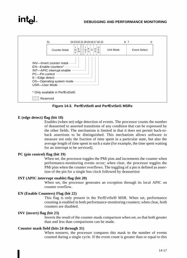
2System Architecture Overview
2-1
CHAPTER 2SYSTEM ARCHITECTURE OVERVIEW
The 32-bit members of the Intel Architecture family of processors provide extensive support foroperating-system and system-development software. This support is part of the processor’ssystem-level architecture and includes features to assist in the following operations:
• Memory management
• Protection of software modules
• Multitasking
• Exception and interrupt handling
• Multiprocessing
• Cache management
• Hardware resource and power management
• Debugging and performance monitoring
This chapter provides a brief overview of the processor’s system-level architecture; a detaileddescription of each part of this architecture given in the following chapters. This chapter alsodescribes the system registers that are used to set up and control the processor at the system leveland gives a brief overview of the processor’s system-level (operating system) instructions.
Many of the system-level architectural features of the processor are used only by systemprogrammers. Application programmers may need to read this chapter, and the following chap-ters which describe the use of these features, in order to understand the hardware facilities usedby system programmers to create a reliable and secure environment for application programs.
NOTE
This overview and most of the subsequent chapters of this book focus on the“native” or protected-mode operation of the 32-bit Intel Architectureprocessors. As described in Chapter 8, Processor Management and Initial-ization, all Intel Architecture processors enter real-address mode following apower-up or reset. Software must then initiate a switch from real-addressmode to protected mode.
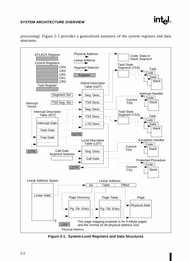
2.1. OVERVIEW OF THE SYSTEM-LEVEL ARCHITECTURE
The Intel Architecture’s system architecture consists of a set of registers, data structures, andinstructions designed to support basic system-level operations such as memory management,interrupt and exception handling, task management, and control of multiple processors (multi-
2-2
SYSTEM ARCHITECTURE OVERVIEW
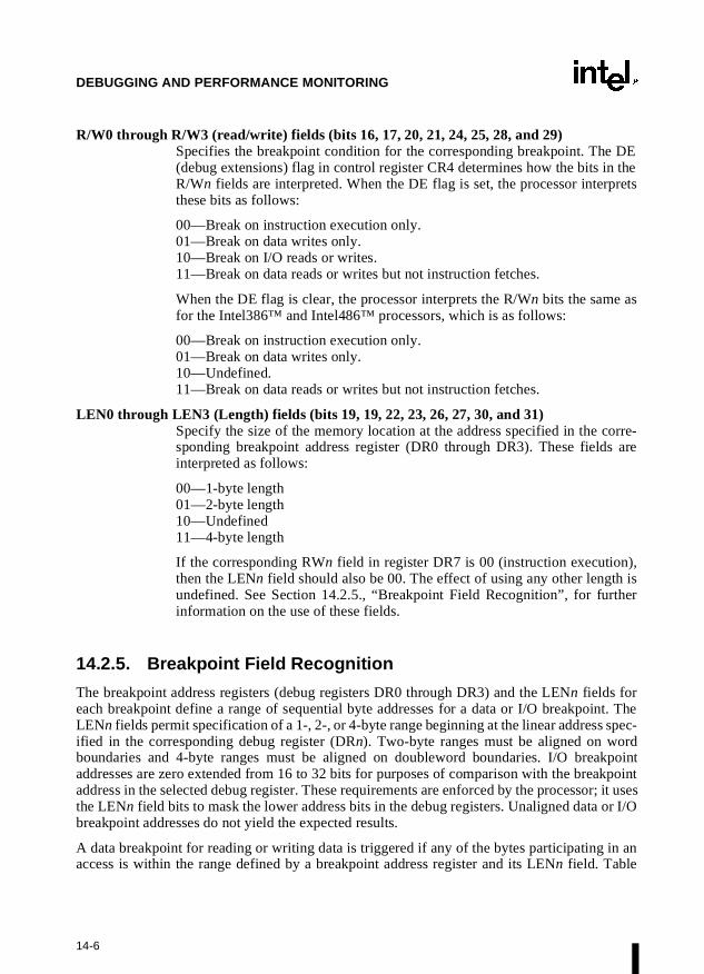
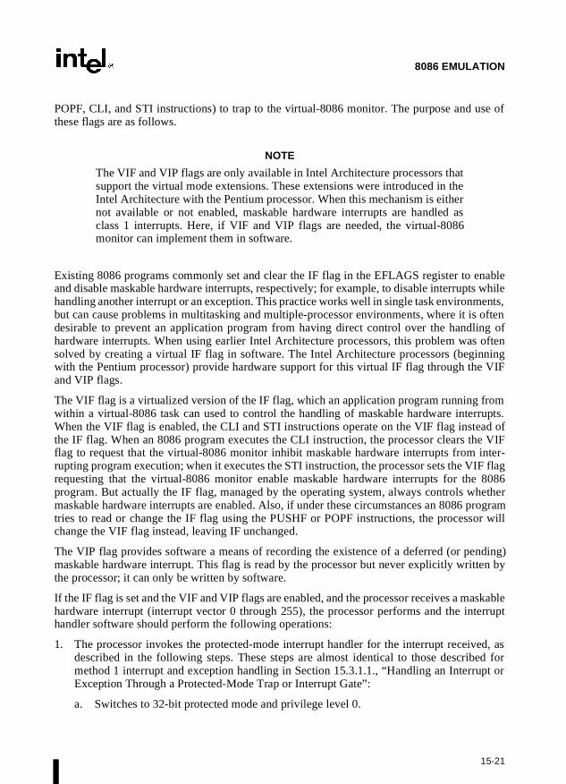
processing). Figure 2-1 provides a generalized summary of the system registers and datastructures.
Figure 2-1. System-Level Registers and Data Structures
Local DescriptorTable (LDT)
EFLAGS Register
Control Registers
CR1CR2CR3CR4
CR0 Global DescriptorTable (GDT)
Interrupt DescriptorTable (IDT)
IDTR
GDTR
Interrupt Gate
Trap Gate
LTD Desc.
TSS Desc.
Code
Stack
CodeStack
CodeStack
Task-StateSegment (TSS)
CodeData
Stack
Task
Interrupt Handler
Exception Handler
Protected Procedure
TSS Seg. Sel.
Call-GateSegment Selector
Dir Table OffsetLinear Address
Page Directory
Pg. Dir. Entry
Linear Address Space
Linear Addr.
0
Seg. Desc.Segment Sel.
Code, Data orStack Segment
InterruptVector
TSS Desc.
Seg. Desc.
Task Gate
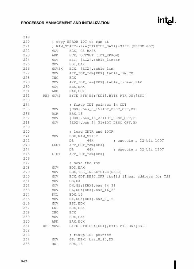
CurrentTSS
Call Gate
Task-StateSegment (TSS)
CodeData
Stack
Task
Seg. Desc.
CurrentTSS
CurrentTSS
Segment Selector
Linear Address
Task Register
CR3*
Page Table
Pg. Tbl. Entry
Page
Physical Addr.
LDTR
This page mapping example is for 4-KByte pagesand the normal 32-bit physical address size.
Register
*Physical Address
Physical Address
2-3
SYSTEM ARCHITECTURE OVERVIEW
2.1.1. Global and Local Descriptor Tables
When operating in protected mode, all memory accesses pass through either the globaldescriptor table (GDT) or the (optional) local descriptor table (LDT), shown in Figure 2-1.These tables contain entries called segment descriptors. A segment descriptor provides the baseaddress of a segment and access rights, type, and usage information. Each segment descriptorhas a segment selector associated with it. The segment selector provides an index into the GDTor LDT (to its associated segment descriptor), a global/local flag (that determines whether thesegment selector points to the GDT or the LDT), and access rights information.
To access a byte in a segment, both a segment selector and an offset must be supplied. Thesegment selector provides access to the segment descriptor for the segment (in the GDT orLDT). From the segment descriptor, the processor obtains the base address of the segment in thelinear address space. The offset then provides the location of the byte relative to the baseaddress. This mechanism can be used to access any valid code, data, or stack segment in theGDT or LDT, provided the segment is accessible from the current privilege level (CPL) at whichthe processor is operating. (The CPL is defined as the protection level of the currently executingcode segment.)
In Figure 2-1 the solid arrows indicate a linear address, the dashed lines indicate a segmentselector, and the dotted arrows indicate a physical address. For simplicity, many of the segmentselectors are shown as direct pointers to a segment. However, the actual path from a segmentselector to its associated segment is always through the GDT or LDT.
The linear address of the base of the GDT is contained in the GDT register (GDTR); the linearaddress of the LDT is contained in the LDT register (LDTR).
2.1.2. System Segments, Segment Descriptors, and Gates
Besides the code, data, and stack segments that make up the execution environment of a programor procedure, the system architecture also defines two system segments: the task-state segment(TSS) and the LDT. (The GDT is not considered a segment because it is not accessed by meansof a segment selector and segment descriptor.) Each of these segment types has a segmentdescriptor defined for it.
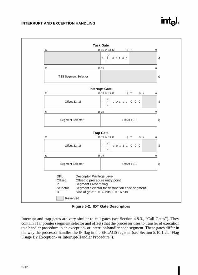
The system architecture also defines a set of special descriptors called gates (the call gate, inter-rupt gate, trap gate, and task gate) that provide protected gateways to system procedures andhandlers that operate at different privilege levels than application programs and procedures.For example, a CALL to a call gate provides access to a procedure in a code segment that is atthe same or numerically lower privilege level (more privileged) than the current code segment.To access a procedure through a call gate, the calling procedure1 must supply the selector of thecall gate. The processor than performs an access rights check on the call gate, comparing theCPL with the privilege level of the call gate and the destination code segment pointed to by thecall gate. If access to the destination code segment is allowed, the processor gets the segmentselector for the destination code segment and an offset into that code segment from the call gate.
1. The word “procedure” is commonly used in this document as a general term for a logical unit or block ofcode (such as a program, procedure, function, or routine). The term is not restricted to the definition of aprocedure in the Intel Architecture assembly language.
2-4
SYSTEM ARCHITECTURE OVERVIEW
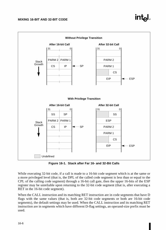
If the call requires a change in privilege level, the processor also switches to the stack for thatprivilege level. (The segment selector for the new stack is obtained from the TSS for thecurrently running task.) Gates also facilitate transitions between 16-bit and 32-bit codesegments, and vice versa.
2.1.3. Task-State Segments and Task Gates
The TSS (see Figure 2-1) defines the state of the execution environment for a task. It includesthe state of the general-purpose registers, the segment registers, the EFLAGS register, the EIPregister, and segment selectors and stack pointers for three stack segments (one stack each forprivilege levels 0, 1, and 2). It also includes the segment selector for the LDT associated withthe task and the page-table base address.
All program execution in protected mode happens within the context of a task, called the currenttask. The segment selector for the TSS for the current task is stored in the task register. Thesimplest method of switching to a task is to make a call or jump to the task. Here, the segmentselector for the TSS of the new task is given in the CALL or JMP instruction. In switching tasks,the processor performs the following actions:
1. Stores the state of the current task in the current TSS.
2. Loads the task register with the segment selector for the new task.
3. Accesses the new TSS through a segment descriptor in the GDT.
4. Loads the state of the new task from the new TSS into the general-purpose registers, thesegment registers, the LDTR, control register CR3 (page-table base address), the EFLAGSregister, and the EIP register.
5. Begins execution of the new task.
A task can also be accessed through a task gate. A task gate is similar to a call gate, except thatit provides access (through a segment selector) to a TSS rather than a code segment.
2.1.4. Interrupt and Exception Handling
External interrupts, software interrupts, and exceptions are handled through the interruptdescriptor table (IDT), see Figure 2-1. The IDT contains a collection of gate descriptors, whichprovide access to interrupt and exception handlers. Like the GDT, the IDT is not a segment. Thelinear address of the base of the IDT is contained in the IDT register (IDTR).
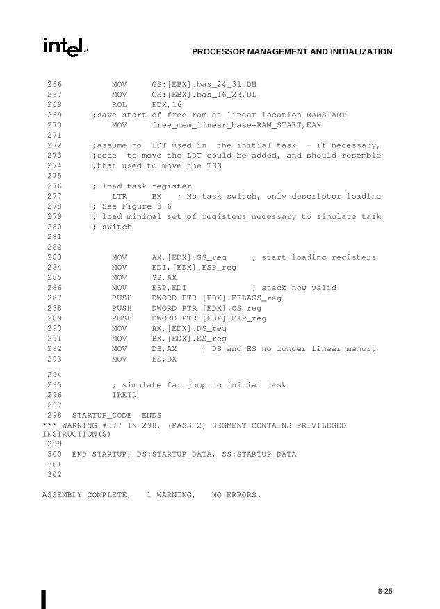
The gate descriptors in the IDT can be of the interrupt-, trap-, or task-gate type. To access aninterrupt or exception handler, the processor must first receive an interrupt vector (interruptnumber) from internal hardware, an external interrupt controller, or from software by means ofan INT, INTO, INT 3, or BOUND instruction. The interrupt vector provides an index into theIDT to a gate descriptor. If the selected gate descriptor is an interrupt gate or a trap gate, the asso-ciated handler procedure is accessed in a manner very similar to calling a procedure through acall gate. If the descriptor is a task gate, the handler is accessed through a task switch.
2-5
SYSTEM ARCHITECTURE OVERVIEW
2.1.5. Memory Management
The system architecture supports either direct physical addressing of memory or virtual memory(through paging). When physical addressing is used, a linear address is treated as a physicaladdress. When paging is used, all the code, data, stack, and system segments and the GDT andIDT can be paged, with only the most recently accessed pages being held in physical memory.
The location of pages (or page frames as they are sometimes called in the Intel Architecture) inphysical memory is contained in two types of system data structures (a page directory and a setof page tables), both of which reside in physical memory (see Figure 2-1). An entry in a pagedirectory contains the physical address of the base of a page table, access rights, and memorymanagement information. An entry in a page table contains the physical address of a page frame,access rights, and memory management information. The base physical address of the pagedirectory is contained in control register CR3.
To use this paging mechanism, a linear address is broken into three parts, providing separateoffsets into the page directory, the page table, and the page frame.
A system can have a single page directory or several. For example, each task can have its ownpage directory.
2.1.6. System Registers
To assist in initializing the processor and controlling system operations, the system architectureprovides system flags in the EFLAGS register and several system registers:
• The system flags and IOPL field in the EFLAGS register control task and mode switching,interrupt handling, instruction tracing, and access rights. See Section 2.3., “System Flagsand Fields in the EFLAGS Register”, for a description of these flags.
• The control registers (CR0, CR2, CR3, and CR4) contain a variety of flags and data fieldsfor controlling system-level operations. See Section 2.5., “Control Registers”, for adescription of these flags.
• The debug registers (not shown in Figure 2-1) allow the setting of breakpoints for use indebugging programs and systems software. See Chapter 14, Debugging and PerformanceMonitoring, for a description of these registers.
• The GDTR, LDTR, and IDTR registers contain the linear addresses and sizes (limits) oftheir respective tables. See Section 2.4., “Memory-Management Registers”, for adescription of these registers.
• The task register contains the linear address and size of the TSS for the current task. SeeSection 2.4., “Memory-Management Registers”, for a description of this register.
• Model-specific registers (not shown in Figure 2-1).
The model-specific registers (MSRs) are a group of registers available primarily to operating-system or executive procedures (that is, code running at privilege level 0). These registerscontrol items such as the debug extensions, the performance-monitoring counters, the machine-check architecture, and the memory type ranges (MTRRs). The number and functions of theseregisters varies among the different members of the Intel Architecture processor families.
2-6
SYSTEM ARCHITECTURE OVERVIEW
Section 8.4., “Model-Specific Registers (MSRs)”, for more information about the MSRs andAppendix B, Model-Specific Registers (MSRs), for a complete list of the MSRs.
Most systems restrict access to all system registers (other than the EFLAGS register) by appli-cation programs. Systems can be designed, however, where all programs and procedures run atthe most privileged level (privilege level 0), in which case application programs are allowed tomodify the system registers.
2.1.7. Other System Resources
Besides the system registers and data structures described in the previous sections, the systemarchitecture provides the following additional resources:
• Operating system instructions (see Section 2.6., “System Instruction Summary”).
• Performance-monitoring counters (not shown in Figure 2-1).
• Internal caches and buffers (not shown in Figure 2-1).
The performance-monitoring counters are event counters that can be programmed to countprocessor events such as the number of instructions decoded, the number of interrupts received,or the number of cache loads. See Section 14.6., “Performance-Monitoring Counters”, for moreinformation about these counters.
The processor provides several internal caches and buffers. The caches are used to store bothdata and instructions. The buffers are used to store things like decoded addresses to system andapplication segments and write operations waiting to be performed. See Chapter 9, MemoryCache Control, for a detailed discussion of the processor’s caches and buffers.
2.2. MODES OF OPERATION
The Intel Architecture supports three operating modes and one quasi-operating mode:
• Protected mode. This is the native operating mode of the processor. In this mode allinstructions and architectural features are available, providing the highest performance andcapability. This is the recommended mode for all new applications and operating systems.
• Real-address mode. This operating mode provides the programming environment of theIntel 8086 processor, with a few extensions (such as the ability to switch to protected orsystem management mode).
• System management mode (SMM). The system management mode (SMM) is a standardarchitectural feature in all Intel Architecture processors, beginning with the Intel386™ SLprocessor. This mode provides an operating system or executive with a transparentmechanism for implementing power management and OEM differentiation features. SMMis entered through activation of an external system interrupt pin (SMI#), which generates asystem management interrupt (SMI). In SMM, the processor switches to a separate addressspace while saving the context of the currently running program or task. SMM-specific
2-7
SYSTEM ARCHITECTURE OVERVIEW
code may then be executed transparently. Upon returning from SMM, the processor isplaced back into its state prior to the SMI.
• Virtual-8086 mode. In protected mode, the processor supports a quasi-operating modeknown as virtual-8086 mode. This mode allows the processor execute 8086 software in aprotected, multitasking environment.
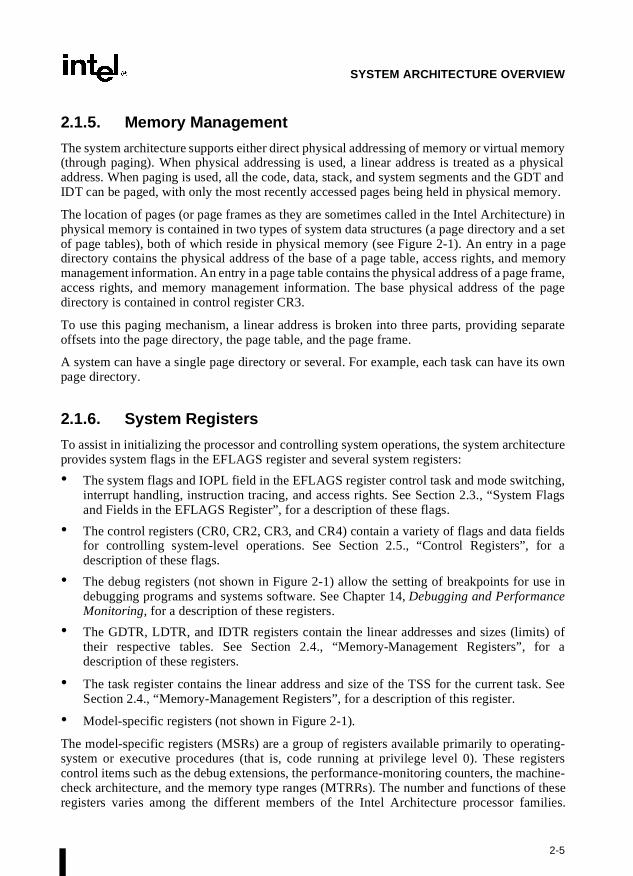
Figure 2-2 shows how the processor moves among these operating modes.
The processor is placed in real-address mode following power-up or a reset. Thereafter, the PEflag in control register CR0 controls whether the processor is operating in real-address orprotected mode (see Section 2.5., “Control Registers”). See Section 8.8., “Mode Switching”, fordetailed information on switching between real-address mode and protected mode.
The VM flag in the EFLAGS register determines whether the processor is operating in protectedmode or virtual-8086 mode. Transitions between protected mode and virtual-8086 mode aregenerally carried out as part of a task switch or a return from an interrupt or exception handler(see Section 15.2.5., “Entering Virtual-8086 Mode”).
The processor switches to SMM whenever it receives an SMI while the processor is in real-address, protected, or virtual-8086 modes. Upon execution of the RSM instruction, theprocessor always returns to the mode it was in when the SMI occurred.
2.3. SYSTEM FLAGS AND FIELDS IN THE EFLAGS REGISTER
The system flags and IOPL field of the EFLAGS register control I/O, maskable hardware inter-rupts, debugging, task switching, and the virtual-8086 mode (see Figure 2-3). Only privilegedcode (typically operating system or executive code) should be allowed to modify these bits.
Figure 2-2. Transitions Among the Processor’s Operating Modes
Real-Address
Protected Mode
Virtual-8086Mode
SystemManagement
Mode
PE=1Reset or
VM=1VM=0
PE=0
Resetor
RSM
SMI#
RSM
SMI#
RSM
SMI#
Reset
Mode
2-8
SYSTEM ARCHITECTURE OVERVIEW
The functions of the system flags and IOPL are as follows:
TF Trap (bit 8). Set to enable single-step mode for debugging; clear to disable single-stepmode. In single-step mode, the processor generates a debug exception after eachinstruction, which allows the execution state of a program to be inspected after eachinstruction. If an application program sets the TF flag using a POPF, POPFD, or IRETinstruction, a debug exception is generated after the instruction that follows the POPF,POPFD, or IRET instruction.
IF Interrupt enable (bit 9). Controls the response of the processor to maskable hardwareinterrupt requests (see Section 5.1.1.2., “Maskable Hardware Interrupts”). Set torespond to maskable hardware interrupts; cleared to inhibit maskable hardware inter-rupts. The IF flag does not effect the generation of exceptions or nonmaskable inter-rupts (NMI interrupts). The CPL, IOPL, and the state of the VME flag in controlregister CR4 determine whether the IF flag can be modified by the CLI, STI, POPF,POPFD, and IRET instructions.
IOPL I/O privilege level field (bits 12 and 13). Indicates the I/O privilege level (IOPL) ofthe currently running program or task. The CPL of the currently running program ortask must be less than or equal to the IOPL to access the I/O address space. This fieldcan only be modified by the POPF and IRET instructions when operating at a CPL of0. See Chapter 9, Input/Output, of the Intel Architecture Software Developer’s Manual,Volume 1, for more information on the relationship of the IOPL to I/O operations.
The IOPL is also one of the mechanisms that controls the modification of the IF flagand the handling of interrupts in virtual-8086 mode when the virtual mode extensionsare in effect (the VME flag in control register CR4 is set).
Figure 2-3. System Flags in the EFLAGS Register
31 22 21 20 19 18 17 16
RF
ID
AC
VM
VM — Virtual-8086 ModeRF — Resume FlagNT — Nested Task FlagIOPL— I/O Privilege LevelIF — Interrupt Enable Flag
AC — Alignment Check
ID — Identification FlagVIP — Virtual Interrupt Pending
15 1314 12 11 10 9 8 7 6 5 4 3 2 1 0
0 CF
AF
PF 1D
FIF
TF
SF
ZF
NT 00
VIP
VIF
OF
IOPL
VIF — Virtual Interrupt Flag
TF — Trap Flag
Reserved
Reserved (set to 0)
2-9
SYSTEM ARCHITECTURE OVERVIEW
NT Nested task (bit 14). Controls the chaining of interrupted and called tasks. Theprocessor sets this flag on calls to a task initiated with a CALL instruction, an interrupt,or an exception. It examines and modifies this flag on returns from a task initiated withthe IRET instruction. The flag can be explicitly set or cleared with the POPF/POPFDinstructions; however, changing to the state of this flag can generate unexpected excep-tions in application programs. See Section 6.4., “Task Linking”, for more informationon nested tasks.
RF Resume (bit 16). Controls the processor’s response to instruction-breakpoint condi-tions. When set, this flag temporarily disables debug exceptions (#DE) from beinggenerated for instruction breakpoints; although, other exception conditions cancause an exception to be generated. When clear, instruction breakpoints will generatedebug exceptions.
The primary function of the RF flag is to allow the restarting of an instruction followinga debug exception that was caused by an instruction breakpoint condition. Here,debugger software must set this flag in the EFLAGS image on the stack just prior toreturning to the interrupted program with the IRETD instruction, to prevent the instruc-tion breakpoint from causing another debug exception. The processor then automati-cally clears this flag after the instruction returned to has been successfully executed,enabling instruction breakpoint faults again.
See Section 14.3.1.1., “Instruction-Breakpoint Exception Condition”, for more infor-mation on the use of this flag.
VM Virtual-8086 mode (bit 17). Set to enable virtual-8086 mode; clear to return toprotected mode. See Section 15.2.1., “Enabling Virtual-8086 Mode”, for a detaileddescription of the use of this flag to switch to virtual-8086 mode.
AC Alignment check (bit 18). Set this flag and the AM flag in the CR0 register to enablealignment checking of memory references; clear the AC flag and/or the AM flag todisable alignment checking. An alignment-check exception is generated when refer-ence is made to an unaligned operand, such as a word at an odd byte address or adoubleword at an address which is not an integral multiple of four. Alignment-checkexceptions are generated only in user mode (privilege level 3). Memory references thatdefault to privilege level 0, such as segment descriptor loads, do not generate thisexception even when caused by instructions executed in user-mode.
The alignment-check exception can be used to check alignment of data. This is usefulwhen exchanging data with other processors, which require all data to be aligned. Thealignment-check exception can also be used by interpreters to flag some pointers asspecial by misaligning the pointer. This eliminates overhead of checking each pointerand only handles the special pointer when used.
VIF Virtual Interrupt (bit 19). Contains a virtual image of the IF flag. This flag is used inconjunction with the VIP flag. The processor only recognizes the VIF flag when eitherthe VME flag or the PVI flag in control register CR4 is set and the IOPL is less than 3.(The VME flag enables the virtual-8086 mode extensions; the PVI flag enables theprotected-mode virtual interrupts.) See Section 15.3.3.5., “Method 6: Software Inter-
2-10
SYSTEM ARCHITECTURE OVERVIEW
rupt Handling”, and Section 15.4., “Protected-Mode Virtual Interrupts”, for detailedinformation about the use of this flag.
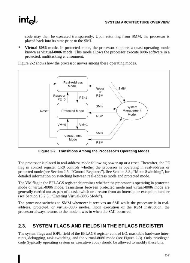
VIP Virtual interrupt pending (bit 20). Set by software to indicate that an interrupt ispending; cleared to indicate that no interrupt is pending. This flag is used in conjunc-tion with the VIF flag. The processor reads this flag but never modifies it. Theprocessor only recognizes the VIP flag when either the VME flag or the PVI flag incontrol register CR4 is set and the IOPL is less than 3. (The VME flag enables thevirtual-8086 mode extensions; the PVI flag enables the protected-mode virtual inter-rupts.) See Section 15.3.3.5., “Method 6: Software Interrupt Handling”, and Section15.4., “Protected-Mode Virtual Interrupts”, for detailed information about the use ofthis flag.
ID Identification (bit 21). The ability of a program or procedure to set or clear this flagindicates support for the CPUID instruction.
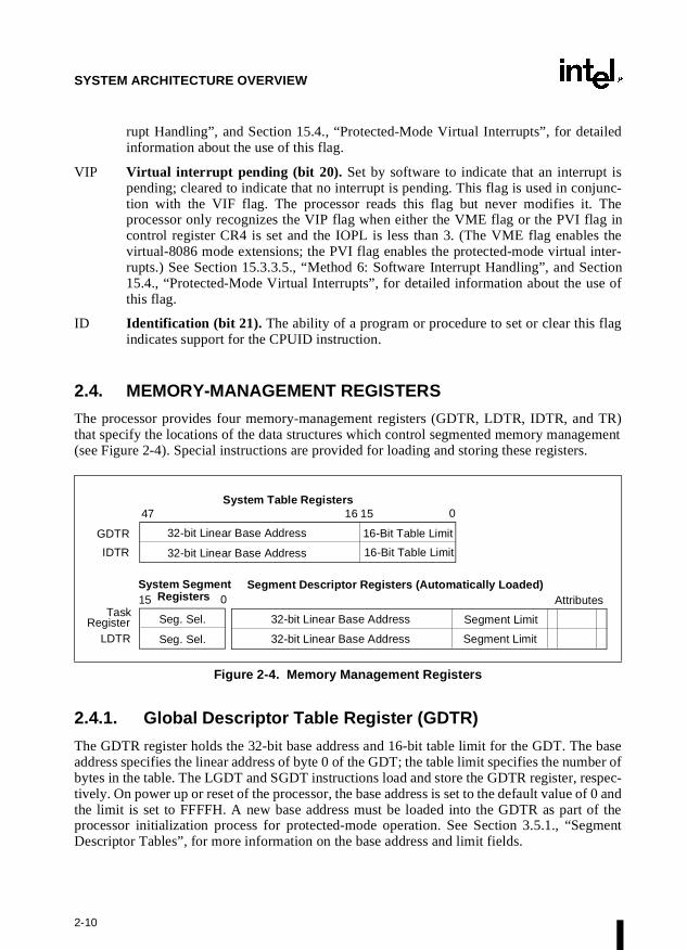
2.4. MEMORY-MANAGEMENT REGISTERS
The processor provides four memory-management registers (GDTR, LDTR, IDTR, and TR)that specify the locations of the data structures which control segmented memory management(see Figure 2-4). Special instructions are provided for loading and storing these registers.
2.4.1. Global Descriptor Table Register (GDTR)
The GDTR register holds the 32-bit base address and 16-bit table limit for the GDT. The baseaddress specifies the linear address of byte 0 of the GDT; the table limit specifies the number ofbytes in the table. The LGDT and SGDT instructions load and store the GDTR register, respec-tively. On power up or reset of the processor, the base address is set to the default value of 0 andthe limit is set to FFFFH. A new base address must be loaded into the GDTR as part of theprocessor initialization process for protected-mode operation. See Section 3.5.1., “SegmentDescriptor Tables”, for more information on the base address and limit fields.
The LDTR register holds the 16-bit segment selector, 32-bit base address, 16-bit segment limit,and descriptor attributes for the LDT. The base address specifies the linear address of byte 0 ofthe LDT segment; the segment limit specifies the number of bytes in the segment. See Section3.5.1., “Segment Descriptor Tables”, for more information on the base address and limit fields.
The LLDT and SLDT instructions load and store the segment selector part of the LDTR register,respectively. The segment that contains the LDT must have a segment descriptor in the GDT.When the LLDT instruction loads a segment selector in the LDTR, the base address, limit, anddescriptor attributes from the LDT descriptor are automatically loaded into the LDTR.
When a task switch occurs, the LDTR is automatically loaded with the segment selector anddescriptor for the LDT for the new task. The contents of the LDTR are not automatically savedprior to writing the new LDT information into the register.
On power up or reset of the processor, the segment selector and base address are set to thedefault value of 0 and the limit is set to FFFFH.
2.4.3. IDTR Interrupt Descriptor Table Register
The IDTR register holds the 32-bit base address and 16-bit table limit for the IDT. The baseaddress specifies the linear address of byte 0 of the IDT; the table limit specifies the number ofbytes in the table. The LIDT and SIDT instructions load and store the IDTR register, respec-tively. On power up or reset of the processor, the base address is set to the default value of 0 andthe limit is set to FFFFH. The base address and limit in the register can then be changed as partof the processor initialization process. See Section 5.8., “Interrupt Descriptor Table (IDT)”, formore information on the base address and limit fields.
2.4.4. Task Register (TR)
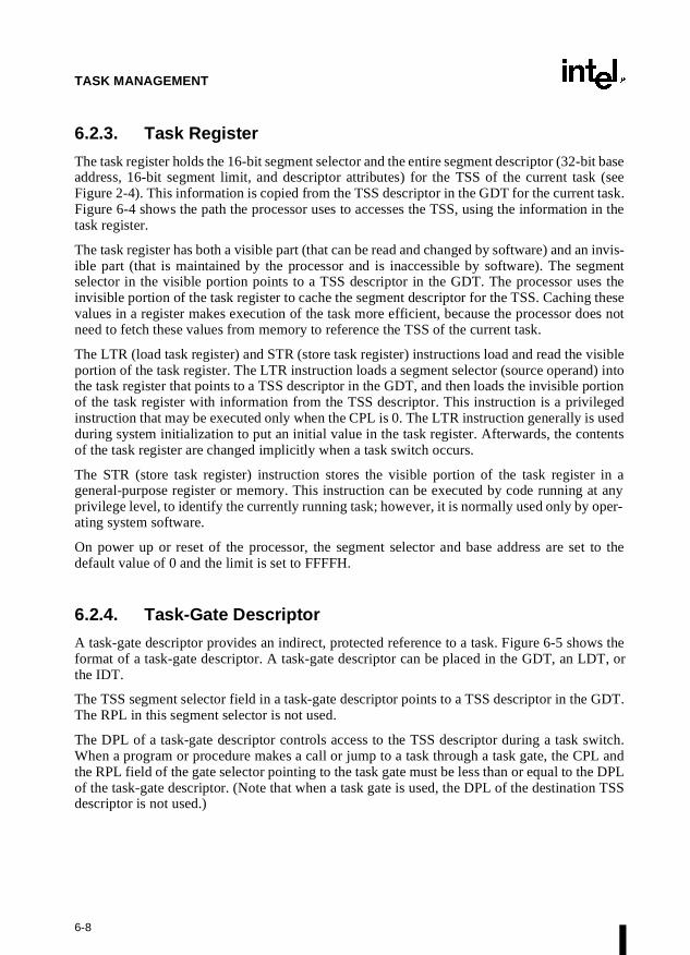
The task register holds the 16-bit segment selector, 32-bit base address, 16-bit segment limit,and descriptor attributes for the TSS of the current task. It references a TSS descriptor in theGDT. The base address specifies the linear address of byte 0 of the TSS; the segment limit spec-ifies the number of bytes in the TSS. (See Section 6.2.3., “Task Register”, for more informationabout the task register.)
The LTR and STR instructions load and store the segment selector part of the task register,respectively. When the LTR instruction loads a segment selector in the task register, the baseaddress, limit, and descriptor attributes from the TSS descriptor are automatically loaded intothe task register. On power up or reset of the processor, the base address is set to the defaultvalue of 0 and the limit is set to FFFFH.
When a task switch occurs, the task register is automatically loaded with the segment selectorand descriptor for the TSS for the new task. The contents of the task register are not automati-cally saved prior to writing the new TSS information into the register.
2-12
SYSTEM ARCHITECTURE OVERVIEW
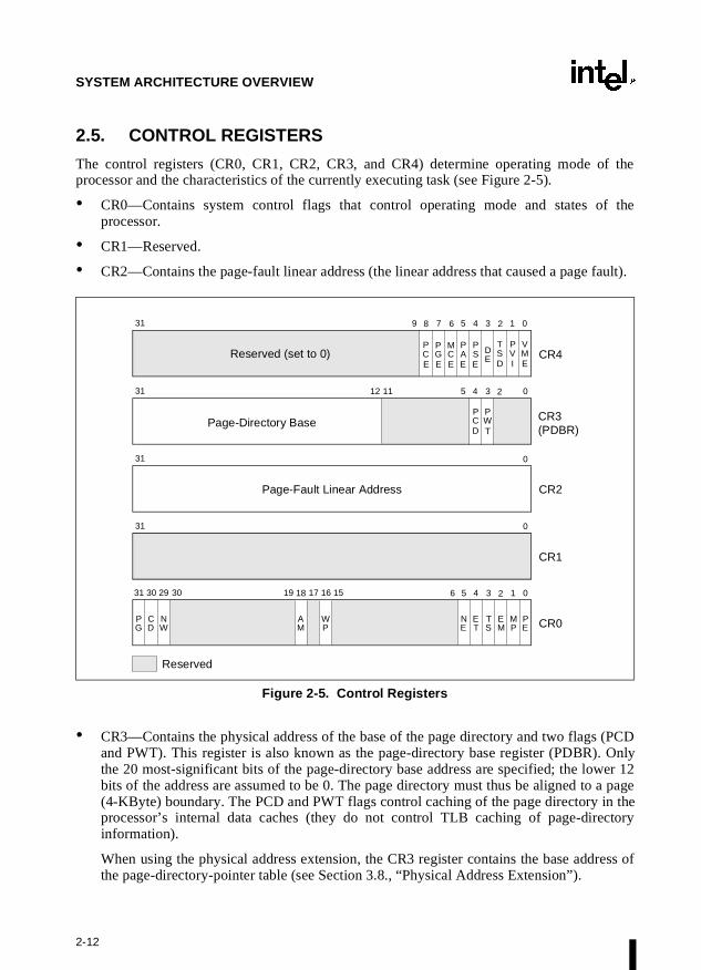
2.5. CONTROL REGISTERS
The control registers (CR0, CR1, CR2, CR3, and CR4) determine operating mode of theprocessor and the characteristics of the currently executing task (see Figure 2-5).
• CR0—Contains system control flags that control operating mode and states of theprocessor.
• CR1—Reserved.
• CR2—Contains the page-fault linear address (the linear address that caused a page fault).
• CR3—Contains the physical address of the base of the page directory and two flags (PCDand PWT). This register is also known as the page-directory base register (PDBR). Onlythe 20 most-significant bits of the page-directory base address are specified; the lower 12bits of the address are assumed to be 0. The page directory must thus be aligned to a page(4-KByte) boundary. The PCD and PWT flags control caching of the page directory in theprocessor’s internal data caches (they do not control TLB caching of page-directoryinformation).
When using the physical address extension, the CR3 register contains the base address ofthe page-directory-pointer table (see Section 3.8., “Physical Address Extension”).
Figure 2-5. Control Registers
CR1
WP
AM
Page-Directory Base
VME
PSE
TSD
DE
PVI
PGE
MCE
PAE
PCE
NW
PG
CD
PWT
PCD
Page-Fault Linear Address
PE
EM
MP
TS
NE
ET
CR2
CR0
CR4
Reserved
CR3
Reserved (set to 0)
31 2930 30 19 18 17 16 15 6 5 4 3 2 1 0
31 0
31 0
31 12 11 5 4 3 2 0
31 9 8 7 6 5 4 3 2 1 0
(PDBR)
2-13
SYSTEM ARCHITECTURE OVERVIEW
• CR4—Contains a group of flags that enable several architectural extensions.
In protected mode, the move-to-or-from-control-registers forms of the MOV instruction allowthe control registers to be read (at any privilege level) or loaded (at privilege level 0 only). Thisrestriction means that application programs (running at privilege levels 1, 2, or 3) are preventedfrom loading the control registers; however, application programs can read these registers. Forexample, an application might need to read register CR0 to determine if an FPU is present.
A program should not attempt to change any of the reserved bit positions. Reserved bits shouldalways be set to the value previously read.
The functions of the flags in the control registers are as follows:
PG Paging (bit 31 of CR0). Enables paging when set; disables paging when clear. Whenpaging is disabled, all linear addresses are treated as physical addresses. The PG flaghas no effect if the PE flag (bit 0 of register CR0) is not also set; in fact, setting the PGflag when the PE flag is clear causes a general-protection exception (#GP) to be gener-ated. See Section 3.6., “Paging (Virtual Memory)”, for a detailed description of theprocessor’s paging mechanism.
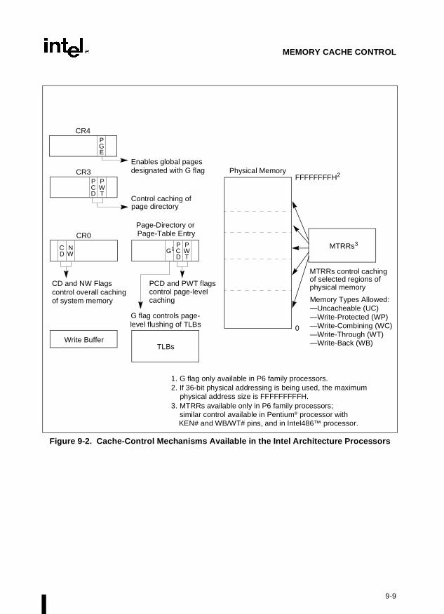
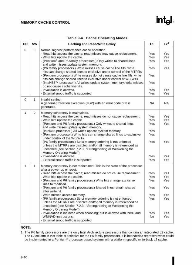
CD Cache Disable (bit 30 of CR0). When the CD and NW flags are clear, caching ofmemory locations for the whole of physical memory in the processor’s internal (andexternal) caches is enabled. When the CD flag is set, caching is restricted as describedin Table 9-4. To prevent the processor from accessing and updating its caches, the CDflag must be set and the caches must be invalidated so that no cache hits can occur (seeSection 9.5.2., “Preventing Caching”). See Section 9.5., “Cache Control”, for adetailed description of the additional restrictions that can be placed on the caching ofselected pages or regions of memory.
NW Not Write-through (bit 29 of CR0). When the NW and CD flags are clear, write-back(for Pentium® and P6 family processors) or write-through (for Intel486™ processors)is enabled for writes that hit the cache and invalidation cycles are enabled. See Table9-4 for detailed information about the affect of the NW flag on caching for othersettings of the CD and NW flags.
AM Alignment Mask (bit 18 of CR0). Enables automatic alignment checking when set;disables alignment checking when clear. Alignment checking is performed only whenthe AM flag is set, the AC flag in the EFLAGS register is set, the CPL is 3, and theprocessor is operating in either protected or virtual-8086 mode.
WP Write Protect (bit 16 of CR0). Inhibits supervisor-level procedures from writing intouser-level read-only pages when set; allows supervisor-level procedures to write intouser-level read-only pages when clear. This flag facilitates implementation of the copy-on-write method of creating a new process (forking) used by operating systems such asUNIX*.
NE Numeric Error (bit 5 of CR0). Enables the native (internal) mechanism for reportingFPU errors when set; enables the PC-style FPU error reporting mechanism when clear.When the NE flag is clear and the IGNNE# input is asserted, FPU errors are ignored.When the NE flag is clear and the IGNNE# input is deasserted, an unmasked FPU errorcauses the processor to assert the FERR# pin to generate an external interrupt and to
2-14
SYSTEM ARCHITECTURE OVERVIEW
stop instruction execution immediately before executing the next waiting floating-point instruction or WAIT/FWAIT instruction. The FERR# pin is intended to drive aninput to an external interrupt controller (the FERR# pin emulates the ERROR# pin ofthe Intel 287 and Intel 387 DX math coprocessors). The NE flag, IGNNE# pin, andFERR# pin are used with external logic to implement PC-style error reporting. (See“Software Exception Handling” in Chapter 7, and Appendix D in the Intel ArchitectureSoftware Developer’s Manual, Volume 1, for more information about FPU errorreporting and for detailed information on when the FERR# pin is asserted, which isimplementation dependent.)
ET Extension Type (bit 4 of CR0). Reserved in the P6 family and Pentium processors.(In the P6 family processors, this flag is hardcoded to 1.) In the Intel386™ and Intel486processors, this flag indicates support of Intel 387 DX math coprocessor instructionswhen set.
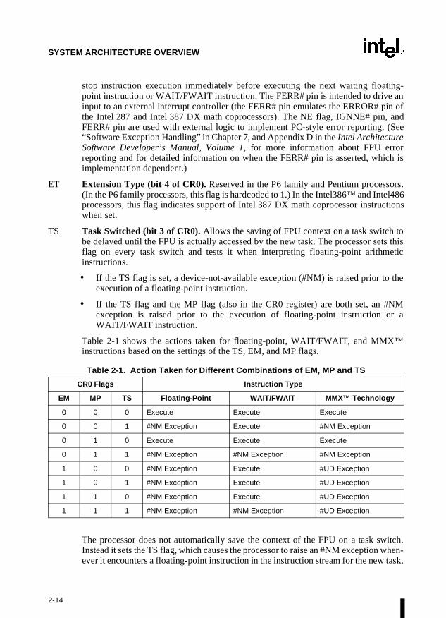
TS Task Switched (bit 3 of CR0). Allows the saving of FPU context on a task switch tobe delayed until the FPU is actually accessed by the new task. The processor sets thisflag on every task switch and tests it when interpreting floating-point arithmeticinstructions.
• If the TS flag is set, a device-not-available exception (#NM) is raised prior to theexecution of a floating-point instruction.
• If the TS flag and the MP flag (also in the CR0 register) are both set, an #NMexception is raised prior to the execution of floating-point instruction or aWAIT/FWAIT instruction.
Table 2-1 shows the actions taken for floating-point, WAIT/FWAIT, and MMX™instructions based on the settings of the TS, EM, and MP flags.
The processor does not automatically save the context of the FPU on a task switch.Instead it sets the TS flag, which causes the processor to raise an #NM exception when-ever it encounters a floating-point instruction in the instruction stream for the new task.
Table 2-1. Action Taken for Different Combinations of EM, MP and TS
CR0 Flags Instruction Type
EM MP TS Floating-Point WAIT/FWAIT MMX™ Technology
0 0 0 Execute Execute Execute
0 0 1 #NM Exception Execute #NM Exception
0 1 0 Execute Execute Execute
0 1 1 #NM Exception #NM Exception #NM Exception
1 0 0 #NM Exception Execute #UD Exception
1 0 1 #NM Exception Execute #UD Exception
1 1 0 #NM Exception Execute #UD Exception
1 1 1 #NM Exception #NM Exception #UD Exception
2-15
SYSTEM ARCHITECTURE OVERVIEW
The fault handler for the #NM exception can then be used to clear the TS flag (with theCLTS instruction) and save the context of the FPU. If the task never encounters afloating-point instruction, the FPU context is never saved.
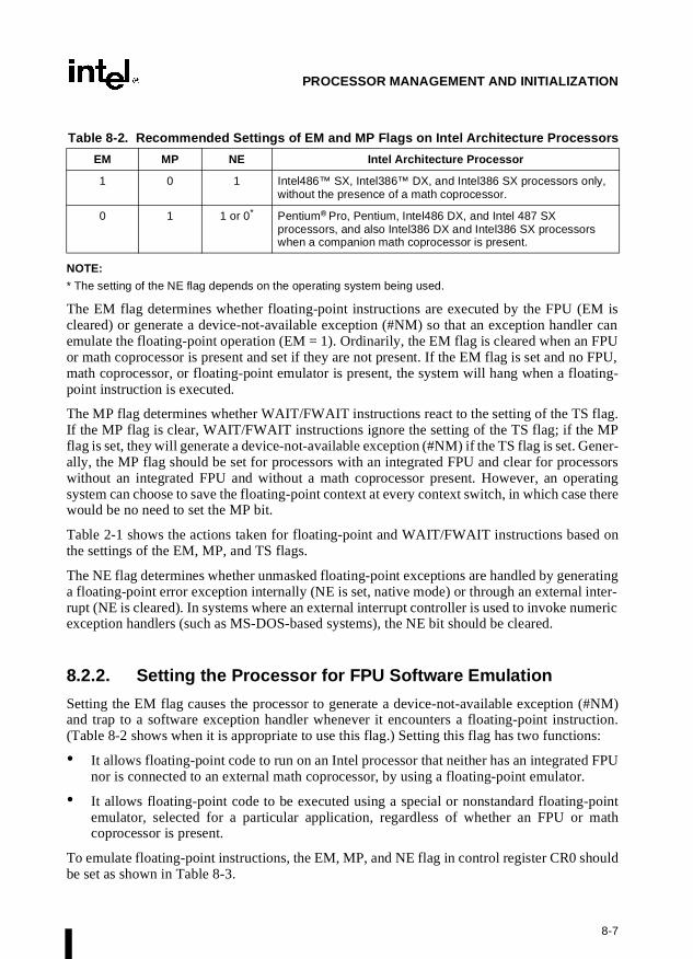
EM Emulation (bit 2 of CR0). Indicates that the processor does not have an internal orexternal FPU when set; indicates an FPU is present when clear. When the EM flag isset, execution of a floating-point instruction generates a device-not-available exception(#NM). This flag must be set when the processor does not have an internal FPU or isnot connected to a math coprocessor. If the processor does have an internal FPU,setting this flag would force all floating-point instructions to be handled by softwareemulation. Table 8-2 shows the recommended setting of this flag, depending on theIntel Architecture processor and FPU or math coprocessor present in the system. Table2-1 shows the interaction of the EM, MP, and TS flags.
Note that the EM flag also affects the execution of the MMX instructions (see Table2-1). When this flag is set, execution of an MMX instructions causes and invalidopcode exception (#UD) to be generated. Thus, if an Intel Architecture processorincorporates MMX technology, the EM flag must be set to 0 to enable execution ofMMX instructions.
MP Monitor Coprocessor (bit 1 of CR0). Controls the interaction of the WAIT (orFWAIT) instruction with the TS flag (bit 3 of CR0). If the MP flag is set, a WAITinstruction generates a device-not-available exception (#NM) if the TS flag is set. If theMP flag is clear, the WAIT instruction ignores the setting of the TS flag. Table 8-2shows the recommended setting of this flag, depending on the Intel Architectureprocessor and FPU or math coprocessor present in the system. Table 2-1 shows theinteraction of the MP, EM, and TS flags.
PE Protection Enable (bit 0 of CR0). Enables protected mode when set; enables real-address mode when clear. This flag does not enable paging directly. It only enablessegment-level protection. To enable paging, both the PE and PG flags must be set. SeeSection 8.8., “Mode Switching”, for information using the PE flag to switch betweenreal and protected mode.
PCD Page-level Cache Disable (bit 4 of CR3). Controls caching of the current page direc-tory. When the PCD flag is set, caching of the page-directory is prevented; when theflag is clear, the page-directory can be cached. This flag affects only the processor’sinternal caches (both L1 and L2, when present). The processor ignores this flag ifpaging is not used (the PG flag in register CR0 is clear) or the CD (cache disable) flagin CR0 is set. See Chapter 9, Memory Cache Control, for more information about theuse of this flag. See Section 3.6.4., “Page-Directory and Page-Table Entries”, for adescription of a companion PCD flag in the page-directory and page-table entries.
PWT Page-level Writes Transparent (bit 3 of CR3). Controls the write-through or write-back caching policy of the current page directory. When the PWT flag is set, write-through caching is enabled; when the flag is clear, write-back caching is enabled. Thisflag affects only the internal caches (both L1 and L2, when present). The processorignores this flag if paging is not used (the PG flag in register CR0 is clear) or the CD(cache disable) flag in CR0 is set. See Section 9.5., “Cache Control”, for more infor-mation about the use of this flag. See Section 3.6.4., “Page-Directory and Page-Table
2-16
SYSTEM ARCHITECTURE OVERVIEW
Entries”, for a description of a companion PCD flag in the page-directory and page-table entries.
VME Virtual-8086 Mode Extensions (bit 0 of CR4). Enables interrupt- and exception-handling extensions in virtual-8086 mode when set; disables the extensions when clear.Use of the virtual mode extensions can improve the performance of virtual-8086 appli-cations by eliminating the overhead of calling the virtual-8086 monitor to handle inter-rupts and exceptions that occur while executing an 8086 program and, instead,redirecting the interrupts and exceptions back to the 8086 program’s handlers. It alsoprovides hardware support for a virtual interrupt flag (VIF) to improve reliability ofrunning 8086 programs in multitasking and multiple-processor environments. SeeSection 15.3., “Interrupt and Exception Handling in Virtual-8086 Mode”, for detailedinformation about the use of this feature.
PVI Protected-Mode Virtual Interrupts (bit 1 of CR4). Enables hardware support for avirtual interrupt flag (VIF) in protected mode when set; disables the VIF flag inprotected mode when clear. See Section 15.4., “Protected-Mode Virtual Interrupts”,for detailed information about the use of this feature.
TSD Time Stamp Disable (bit 2 of CR4). Restricts the execution of the RDTSC instructionto procedures running at privilege level 0 when set; allows RDTSC instruction to beexecuted at any privilege level when clear.
DE Debugging Extensions (bit 3 of CR4). References to debug registers DR4 and DR5cause an undefined opcode (#UD) exception to be generated when set; when clear,processor aliases references to registers DR4 and DR5 for compatibility with softwarewritten to run on earlier Intel Architecture processors. See Section 14.2.2., “DebugRegisters DR4 and DR5”, for more information on the function of this flag.
PSE Page Size Extensions (bit 4 of CR4). Enables 4-MByte pages when set; restricts pagesto 4 KBytes when clear. See Section 3.6.1., “Paging Options”, for more informationabout the use of this flag.
PAE Physical Address Extension (bit 5 of CR4). Enables paging mechanism to reference36-bit physical addresses when set; restricts physical addresses to 32 bits when clear.See Section 3.8., “Physical Address Extension”, for more information about the phys-ical address extension.
MCE Machine-Check Enable (bit 6 of CR4). Enables the machine-check exception whenset; disables the machine-check exception when clear. See Chapter 12, Machine-CheckArchitecture, for more information about the machine-check exception and machine-check architecture.
PGE Page Global Enable (bit 7 of CR4). (Introduced in the P6 family processors.) Enablesthe global page feature when set; disables the global page feature when clear. Theglobal page feature allows frequently used or shared pages to be marked as global toall users (done with the global flag, bit 8, in a page-directory or page-table entry).Global pages are not flushed from the translation-lookaside buffer (TLB) on a taskswitch or a write to register CR3. See Section 3.7., “Translation Lookaside Buffers(TLBs)”, for more information on the use of this bit.
2-17
SYSTEM ARCHITECTURE OVERVIEW
PCE Performance-Monitoring Counter Enable (bit 8 of CR4). Enables execution of theRDPMC instruction for programs or procedures running at any protection level whenset; RDPMC instruction can be executed only at protection level 0 when clear.
2.5.1. CPUID Qualification of Control Register Flags
The VME, PVI, TSD, DE, PSE, PAE, MCE, PGE, and PCE flags in control register CR4 aremodel specific. All of these flags (except the PCE flag) can be qualified with the CPUID instruc-tion to determine if they are implemented on the processor before they are used.
2.6. SYSTEM INSTRUCTION SUMMARY
The system instructions handle system-level functions such as loading system registers,managing the cache, managing interrupts, or setting up the debug registers. Many of theseinstructions can be executed only by operating-system or executive procedures (that is, proce-dures running at privilege level 0). Others can be executed at any privilege level and are thusavailable to application programs. Table 2-2 lists the system instructions and indicates whetherthey are available and useful for application programs. These instructions are described in detailin Chapter 3, Instruction Set Reference, of the Intel Architecture Software Developer’s Manual,Volume 2.:
Table 2-2. Summary of System Instructions
Instruction DescriptionUseful to
Application?Protected fromApplication?
LLDT Load LDT Register No Yes
SLDT Store LDT Register No No
LGDT Load GDT Register No Yes
SGDT Store GDT Register No No
LTR Load Task Register No Yes
STR Store Task Register No No
LIDT Load IDT Register No Yes
SIDT Store IDT Register No No
MOV CRn Load and store control registers Yes Yes (load only)
SMSW Store MSW Yes No
LMSW Load MSW No Yes
CLTS Clear TS flag in CR0 No Yes
ARPL Adjust RPL Yes1 No
LAR Load Access Rights Yes No
LSL Load Segment Limit Yes No
2-18
SYSTEM ARCHITECTURE OVERVIEW
NOTES:
1. Useful to application programs running at a CPL of 1 or 2.
2. The TSD and PCE flags in control register CR4 control access to these instructions by applicationprograms running at a CPL of 3.
3. These instructions were introduced into the Intel Architecture with the Pentium® processor.
4. This instruction was introduced into the Intel Architecture with the Pentium Pro processor and the Pen-tium processor with MMX™ technology.
2.6.1. Loading and Storing System Registers
The GDTR, LDTR, IDTR, and TR registers each have a load and store instruction for loadingdata into and storing data from the register:
LGDT (Load GDTR Register) Loads the GDT base address and limit from memory into theGDTR register.
SGDT (Store GDTR Register) Stores the GDT base address and limit from the GDTR registerinto memory.
LIDT (Load IDTR Register) Loads the IDT base address and limit from memory into theIDTR register.
SIDT (Load IDTR Register Stores the IDT base address and limit from the IDTR registerinto memory.
Table 2-2. Summary of System Instructions (Contd.)
2-19
SYSTEM ARCHITECTURE OVERVIEW
LLDT (Load LDT Register) Loads the LDT segment selector and segment descriptor frommemory into the LDTR. (The segment selector operand can alsobe located in a general-purpose register.)
SLDT (Store LDT Register) Stores the LDT segment selector from the LDTR register intomemory or a general-purpose register.
LTR (Load Task Register) Loads segment selector and segment descriptor for a TSS frommemory into the task register. (The segment selector operandcan also be located in a general-purpose register.)
STR (Store Task Register) Store the segment selector for the current task TSS from the taskregister into memory or a general-purpose register.
The LMSW (load machine status word) and SMSW (store machine status word) instructionsoperate on bits 0 through 15 of control register CR0. These instructions are provided for compat-ibility with the 16-bit Intel 286 processor. Program written to run on 32-bit Intel Architectureprocessors should not use these instructions. Instead, they should access the control register CR0using the MOV instruction.
The CLTS (clear TS flag in CR0) instruction is provided for use in handling a device-not-avail-able exception (#NM) that occurs when the processor attempts to execute a floating-pointinstruction when the TS flag is set. This instruction allows the TS flag to be cleared after theFPU context has been saved, preventing further #NM exceptions. See Section 2.5., “ControlRegisters”, for more information about the TS flag.
The control registers (CR0, CR1, CR2, CR3, and CR4) are loaded with the MOV instruction.This instruction can load a control register from a general-purpose register or store the contentsof the control register in a general-purpose register.
2.6.2. Verifying of Access Privileges
The processor provides several instructions for examining segment selectors and segmentdescriptors to determine if access to their associated segments is allowed. These instructionsduplicate some of the automatic access rights and type checking done by the processor, thusallowing operating-system or executive software to prevent exceptions from being generated.
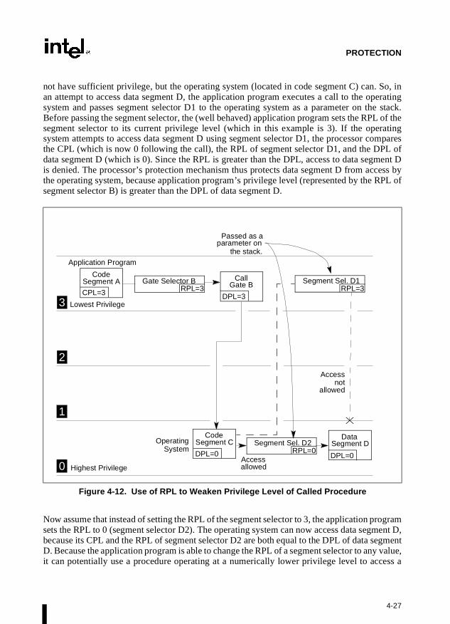
The ARPL (adjust RPL) instruction adjusts the RPL (requestor privilege level) of a segmentselector to match that of the program or procedure that supplied the segment selector. SeeSection 4.10.4., “Checking Caller Access Privileges (ARPL Instruction)”, for a detailed expla-nation of the function and use of this instruction.
The LAR (load access rights) instruction verifies the accessibility of a specified segment andloads the access rights information from the segment’s segment descriptor into a general-purpose register. Software can then examine the access rights to determine if the segment typeis compatible with its intended use. See Section 4.10.1., “Checking Access Rights (LAR Instruc-tion)”, for a detailed explanation of the function and use of this instruction.
The LSL (load segment limit) instruction verifies the accessibility of a specified segment andloads the segment limit from the segment’s segment descriptor into a general-purpose register.
2-20
SYSTEM ARCHITECTURE OVERVIEW
Software can then compare the segment limit with an offset into the segment to determinewhether the offset lies within the segment. See Section 4.10.3., “Checking That the PointerOffset Is Within Limits (LSL Instruction)”, for a detailed explanation of the function and use ofthis instruction.
The VERR (verify for reading) and VERW (verify for writing) instructions verify if a selectedsegment is readable or writable, respectively, at the CPL. See Section 4.10.2., “CheckingRead/Write Rights (VERR and VERW Instructions)”, for a detailed explanation of the functionand use of this instruction.
2.6.3. Loading and Storing Debug Registers
The internal debugging facilities in the processor are controlled by a set of 8 debug registers(DR0 through DR7). The MOV instruction allows setup data to be loaded into and stored fromthese registers.
2.6.4. Invalidating Caches and TLBs
The processor provides several instructions for use in explicitly invalidating its caches and TLBentries. The INVD (invalidate cache with no writeback) instruction invalidates all data andinstruction entries in the internal caches and TLBs and sends a signal to the external caches indi-cating that they should be invalidated also.
The WBINVD (invalidate cache with writeback) instruction performs the same function as theINVD instruction, except that it writes back any modified lines in its internal caches to memorybefore it invalidates the caches. After invalidating the internal caches, it signals the externalcaches to write back modified data and invalidate their contents.
The INVLPG (invalidate TLB entry) instruction invalidates (flushes) the TLB entry for a spec-ified page.
2.6.5. Controlling the Processor
The HLT (halt processor) instruction stops the processor until an enabled interrupt (such as NMIor SMI, which are normally enabled), the BINIT# signal, the INIT# signal, or the RESET#signal is received. The processor generates a special bus cycle to indicate that the halt mode hasbeen entered. Hardware may respond to this signal in a number of ways. An indicator light onthe front panel may be turned on. An NMI interrupt for recording diagnostic information maybe generated. Reset initialization may be invoked. (Note that the BINIT# pin was introducedwith the Pentium Pro processor.)
The LOCK prefix invokes a locked (atomic) read-modify-write operation when modifying amemory operand. This mechanism is used to allow reliable communications between processorsin multiprocessor systems. In the Pentium and earlier Intel Architecture processors, the LOCKprefix causes the processor to assert the LOCK# signal during the instruction, which always
2-21
SYSTEM ARCHITECTURE OVERVIEW
causes an explicit bus lock to occur. In the P6 family processors, the locking operation ishandled with either a cache lock or bus lock. If a memory access is cacheable and affects onlya single cache line, a cache lock is invoked and the system bus and the actual memory locationin system memory are not locked during the operation. Here, other P6 family processors on thebus write-back any modified data and invalidate their caches as necessary to maintain systemmemory coherency. If the memory access is not cacheable and/or it crosses a cache lineboundary, the processor’s LOCK# signal is asserted and the processor does not respond torequests for bus control during the locked operation.
The RSM (return from SMM) instruction restores the processor (from a context dump) to thestate it was in prior to an system management mode (SMM) interrupt.
2.6.6. Reading Performance-Monitoring and Time-Stamp Counters
The RDPMC (read performance-monitoring counter) and RDTSC (read time-stamp counter)instructions allow an application program to read the processors performance-monitoring andtime-stamp counters, respectively.
The P6 family processors have two 40-bit performance counters that record either the occur-rence of events or the duration of events. The events that can be monitored include the numberof instructions decoded, number of interrupts received, of number of cache loads. Each countercan be set up to monitor a different event, using the system instruction WRMSR to set up valuesin the model-specific registers PerfEvtSel0 and PerfEvtSel1. The RDPMC instruction loads thecurrent count in counter 0 or 1 into the EDX:EAX registers.
The time-stamp counter is a model-specific 64-bit counter that is reset to zero each time theprocessor is reset. If not reset, the counter will increment ~6.3 x 10¹⁵ times per year whenthe processor is operating at a clock rate of 200 MHz. At this clock frequency, it would takeover 2000 years for the counter to wrap around. The RDTSC instruction loads the currentcount of the time-stamp counter into the EDX:EAX registers.
See Section 14.6., “Performance-Monitoring Counters”, and Section 14.5., “Time-StampCounter”, for more information about the performance monitoring and time-stamp counters.
The RDTSC instruction was introduced into the Intel Architecture with the Pentium processor.The RDPMC instruction was introduced into the Intel Architecture with the Pentium Proprocessor and the Pentium processor with MMX technology. Earlier Pentium processors havetwo performance-monitoring counters, but they can be read only with the RDMSR instruction,and only at privilege level 0.
2.6.7. Reading and Writing Model-Specific Registers
The RDMSR (read model-specific register) and WRMSR (write model-specific register) allowthe processor’s 64-bit model-specific registers (MSRs) to be read and written to, respectively.The MSR to be read or written to is specified by the value in the ECX register. The RDMSRinstructions reads the value from the specified MSR into the EDX:EAX registers; the WRMSR
2-22
SYSTEM ARCHITECTURE OVERVIEW
writes the value in the EDX:EAX registers into the specified MSR. See Section 8.4., “Model-Specific Registers (MSRs)”, for more information about the MSRs.
The RDMSR and WRMSR instructions were introduced into the Intel Architecture with thePentium processor.
3Protected-Mode Memory Management
3-1
CHAPTER 3PROTECTED-MODE MEMORY MANAGEMENT
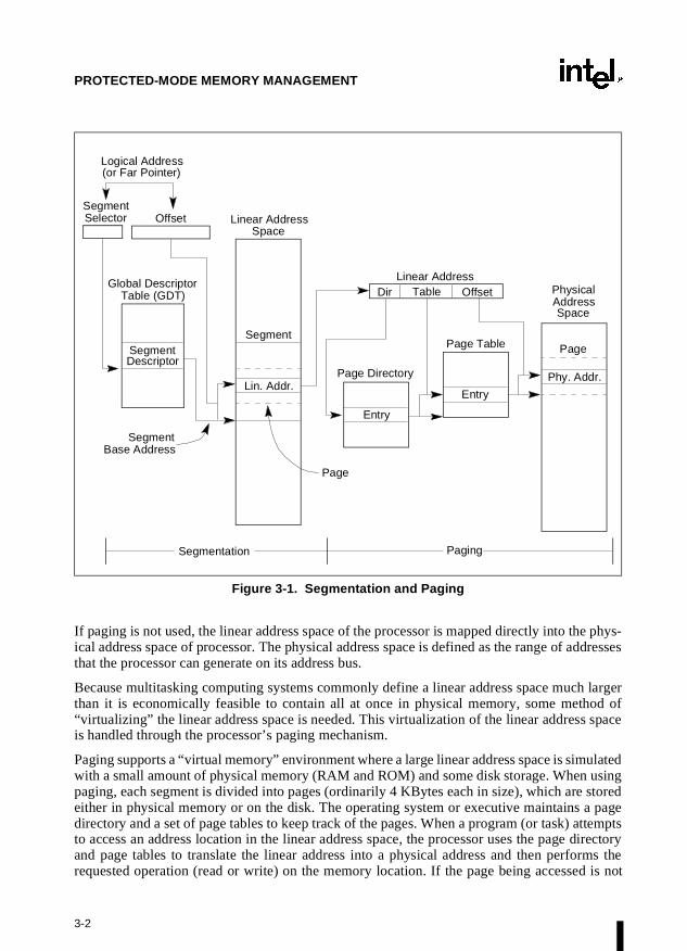
This chapter describes the Intel Architecture’s protected-mode memory management facilities,including the physical memory requirements, the segmentation mechanism, and the pagingmechanism. See Chapter 4, Protection, for a description of the processor’s protection mecha-nism. See Chapter 15, 8086 Emulation, for a description of memory addressing protection inreal-address and virtual-8086 modes.
3.1. MEMORY MANAGEMENT OVERVIEW
The memory management facilities of the Intel Architecture are divided into two parts: segmen-tation and paging. Segmentation provides a mechanism of isolating individual code, data, andstack modules so that multiple programs (or tasks) can run on the same processor without inter-fering with one another. Paging provides a mechanism for implementing a conventionaldemand-paged, virtual-memory system where sections of a program’s execution environmentare mapped into physical memory as needed. Paging can also be used to provide isolationbetween multiple tasks. When operating in protected mode, some form of segmentation must beused. There is no mode bit to disable segmentation. The use of paging, however, is optional.
These two mechanisms (segmentation and paging) can be configured to support simple single-program (or single-task) systems, multitasking systems, or multiple-processor systems that usedshared memory.
As shown in Figure 3-1, segmentation provides a mechanism for dividing the processor’saddressable memory space (called the linear address space) into smaller protected addressspaces called segments. Segments can be used to hold the code, data, and stack for a programor to hold system data structures (such as a TSS or LDT). If more than one program (or task) isrunning on a processor, each program can be assigned its own set of segments. The processorthen enforces the boundaries between these segments and insures that one program does notinterfere with the execution of another program by writing into the other program’s segments.The segmentation mechanism also allows typing of segments so that the operations that may beperformed on a particular type of segment can be restricted.
All of the segments within a system are contained in the processor’s linear address space. Tolocate a byte in a particular segment, a logical address (sometimes called a far pointer) must beprovided. A logical address consists of a segment selector and an offset. The segment selectoris a unique identifier for a segment. Among other things it provides an offset into a descriptortable (such as the global descriptor table, GDT) to a data structure called a segment descriptor.Each segment has a segment descriptor, which specifies the size of the segment, the access rightsand privilege level for the segment, the segment type, and the location of the first byte of thesegment in the linear address space (called the base address of the segment). The offset part ofthe logical address is added to the base address for the segment to locate a byte within thesegment. The base address plus the offset thus forms a linear address in the processor’s linearaddress space.
3-2
PROTECTED-MODE MEMORY MANAGEMENT
If paging is not used, the linear address space of the processor is mapped directly into the phys-ical address space of processor. The physical address space is defined as the range of addressesthat the processor can generate on its address bus.
Because multitasking computing systems commonly define a linear address space much largerthan it is economically feasible to contain all at once in physical memory, some method of“virtualizing” the linear address space is needed. This virtualization of the linear address spaceis handled through the processor’s paging mechanism.
Paging supports a “virtual memory” environment where a large linear address space is simulatedwith a small amount of physical memory (RAM and ROM) and some disk storage. When usingpaging, each segment is divided into pages (ordinarily 4 KBytes each in size), which are storedeither in physical memory or on the disk. The operating system or executive maintains a pagedirectory and a set of page tables to keep track of the pages. When a program (or task) attemptsto access an address location in the linear address space, the processor uses the page directoryand page tables to translate the linear address into a physical address and then performs therequested operation (read or write) on the memory location. If the page being accessed is not
Figure 3-1. Segmentation and Paging
Global DescriptorTable (GDT)
Linear AddressSpace
SegmentSegmentDescriptor
Offset
Logical Address
SegmentBase Address
Page
Phy. Addr.Lin. Addr.
SegmentSelector
Dir Table OffsetLinear Address
Page Table
Page Directory
Entry
Physical
Space
Entry
(or Far Pointer)
PagingSegmentation
Address
Page
3-3
PROTECTED-MODE MEMORY MANAGEMENT
currently in physical memory, the processor interrupts execution of the program (by generatinga page-fault exception). The operating system or executive then reads the page into physicalmemory from the disk and continues executing the program.
When paging is implemented properly in the operating-system or executive, the swapping ofpages between physical memory and the disk is transparent to the correct execution of aprogram. Even programs written for 16-bit Intel Architecture processors can be paged (transpar-ently) when they are run in virtual-8086 mode.
3.2. USING SEGMENTS
The segmentation mechanism supported by the Intel Architecture can be used to implement awide variety of system designs. These designs range from flat models that make only minimaluse of segmentation to protect programs to multisegmented models that employ segmentationto create a robust operating environment in which multiple programs and tasks can be executedreliably.
The following sections give several examples of how segmentation can be employed in a systemto improve memory management performance and reliability.
3.2.1. Basic Flat Model
The simplest memory model for a system is the basic “flat model,” in which the operatingsystem and application programs have access to a continuous, unsegmented address space. Tothe greatest extent possible, this basic flat model hides the segmentation mechanism of the archi-tecture from both the system designer and the application programmer.
To implement a basic flat memory model with the Intel Architecture, at least two segmentdescriptors must be created, one for referencing a code segment and one for referencing a datasegment (see Figure 3-2). Both of these segments, however, are mapped to the entire linearaddress space: that is, both segment descriptors have the same base address value of 0 and thesame segment limit of 4 GBytes. By setting the segment limit to 4 GBytes, the segmentationmechanism is kept from generating exceptions for out of limit memory references, even if nophysical memory resides at a particular address. ROM (EPROM) is generally located at the topof the physical address space, because the processor begins execution at FFFF_FFF0H. RAM(DRAM) is placed at the bottom of the address space because the initial base address for the DSdata segment after reset initialization is 0.
3-4
PROTECTED-MODE MEMORY MANAGEMENT
3.2.2. Protected Flat Model
The protected flat model is similar to the basic flat model, except the segment limits are set toinclude only the range of addresses for which physical memory actually exists (see Figure 3-3).A general-protection exception (#GP) is then generated on any attempt to access nonexistentmemory. This model provides a minimum level of hardware protection against some kinds ofprogram bugs.
More complexity can be added to this protected flat model to provide more protection. Forexample, for the paging mechanism to provide isolation between user and supervisor code anddata, four segments need to be defined: code and data segments at privilege level 3 for the user,and code and data segments at privilege level 0 for the supervisor. Usually these segments alloverlay each other and start at address 0 in the linear address space. This flat segmentation
Figure 3-2. Flat Model
Figure 3-3. Protected Flat Model
Linear Address Space(or Physical Memory)
Data and
FFFFFFFFHSegment
LimitAccessBase Address
Registers
CS
SS
DS
ES
FS
GS
Code
0
Code- and Data-SegmentDescriptors
Stack
Not Present
Linear Address Space(or Physical Memory)
Data and
FFFFFFFFHSegment
LimitAccessBase Address
Registers
CS
ES
SS
DS
FS
GS
Code
0
SegmentDescriptors
LimitAccessBase Address
Memory I/O
Stack
Not Present
3-5
PROTECTED-MODE MEMORY MANAGEMENT
model along with a simple paging structure can protect the operating system from applications,and by adding a separate paging structure for each task or process, it can also protect applica-tions from each other. Similar designs are used by several popular multitasking operatingsystems.
3.2.3. Multisegment Model
A multisegment model (such as the one shown in Figure 3-4) uses the full capabilities of thesegmentation mechanism to provided hardware enforced protection of code, data structures, andprograms and tasks. Here, each program (or task) is given its own table of segment descriptorsand its own segments. The segments can be completely private to their assigned programs orshared among programs. Access to all segments and to the execution environments of individualprograms running on the system is controlled by hardware.
Figure 3-4. Multisegment Model
Linear Address Space(or Physical Memory)
SegmentRegisters
CS
SegmentDescriptors
LimitAccessBase Address
SS LimitAccessBase Address
DS LimitAccessBase Address
ES LimitAccessBase Address
FS LimitAccessBase Address
GS LimitAccessBase Address
LimitAccessBase Address
LimitAccessBase Address
LimitAccessBase Address
LimitAccessBase Address
Stack
Code
Data
Data
Data
Data
3-6
PROTECTED-MODE MEMORY MANAGEMENT
Access checks can be used to protect not only against referencing an address outside the limitof a segment, but also against performing disallowed operations in certain segments. Forexample, since code segments are designated as read-only segments, hardware can be used toprevent writes into code segments. The access rights information created for segments can alsobe used to set up protection rings or levels. Protection levels can be used to protect operating-system procedures from unauthorized access by application programs.
3.2.4. Paging and Segmentation
Paging can be used with any of the segmentation models described in Figures 3-2, 3-3, and 3-4.The processor’s paging mechanism divides the linear address space (into which segments aremapped) into pages (as shown in Figure 3-1). These linear-address-space pages are then mappedto pages in the physical address space. The paging mechanism offers several page-level protec-tion facilities that can be used with or instead of the segment-protection facilities. For example,it lets read-write protection be enforced on a page-by-page basis. The paging mechanism alsoprovides two-level user-supervisor protection that can also be specified on a page-by-page basis.
3.3. PHYSICAL ADDRESS SPACE
In protected mode, the Intel Architecture provides a normal physical address space of 4 GBytes(232
bytes). This is the address space that the processor can address on its address bus. Thisaddress space is flat (unsegmented), with addresses ranging continuously from 0 toFFFFFFFFH. This physical address space can be mapped to read-write memory, read-onlymemory, and memory mapped I/O. The memory mapping facilities described in this chapter canbe used to divide this physical memory up into segments and/or pages.
(Introduced in the Pentium Pro processor.) The Intel Architecture also supports an extension ofthe physical address space to 236 bytes (64 GBytes), with a maximum physical address ofFFFFFFFFFH. This extension is invoked with the physical address extension (PAE) flag,located in bit 5 of control register CR4. (See Section 3.8., “Physical Address Extension”, formore information about extended physical addressing.)
3.4. LOGICAL AND LINEAR ADDRESSES
At the system-architecture level in protected mode, the processor uses two stages of addresstranslation to arrive at a physical address: logical-address translation and linear address spacepaging.
Even with the minimum use of segments, every byte in the processor’s address space is accessedwith a logical address. A logical address consists of a 16-bit segment selector and a 32-bit offset(see Figure 3-5). The segment selector identifies the segment the byte is located in and the offsetspecifies the location of the byte in the segment relative to the base address of the segment.
The processor translates every logical address into a linear address. A linear address is a 32-bitaddress in the processor’s linear address space. Like the physical address space, the linearaddress space is a flat (unsegmented), 232-byte address space, with addresses ranging from 0 to
3-7
PROTECTED-MODE MEMORY MANAGEMENT
FFFFFFFH. The linear address space contains all the segments and system tables defined for asystem.
To translate a logical address into a linear address, the processor does the following:
1. Uses the offset in the segment selector to locate the segment descriptor for the segment inthe GDT or LDT and reads it into the processor. (This step is needed only when a newsegment selector is loaded into a segment register.)
2. Examines the segment descriptor to check the access rights and range of the segment toinsure that the segment is accessible and that the offset is within the limits of the segment.
3. Adds the base address of the segment from the segment descriptor to the offset to form alinear address.
If paging is not used, the processor maps the linear address directly to a physical address (thatis, the linear address goes out on the processor’s address bus). If the linear address space ispaged, a second level of address translation is used to translate the linear address into a physicaladdress. Page translation is described in Section 3.6., “Paging (Virtual Memory)”.
3.4.1. Segment Selectors
A segment selector is a 16-bit identifier for a segment (see Figure 3-6). It does not point directlyto the segment, but instead points to the segment descriptor that defines the segment. A segmentselector contains the following items:
Index (Bits 3 through 15). Selects one of 8192 descriptors in the GDT or LDT. Theprocessor multiplies the index value by 8 (the number of bytes in a segmentdescriptor) and adds the result to the base address of the GDT or LDT (fromthe GDTR or LDTR register, respectively).
Figure 3-5. Logical Address to Linear Address Translation
Offset0
Base Address
Descriptor Table
SegmentDescriptor
31Seg. Selector
015Logical
Address
+
Linear Address031
3-8
PROTECTED-MODE MEMORY MANAGEMENT
TI (table indicator) flag(Bit 2). Specifies the descriptor table to use: clearing this flag selects the GDT;setting this flag selects the current LDT.
Requested Privilege Level (RPL)(Bits 0 and 1). Specifies the privilege level of the selector. The privilege levelcan range from 0 to 3, with 0 being the most privileged level. See Section 4.5.,“Privilege Levels”, for a description of the relationship of the RPL to the CPLof the executing program (or task) and the descriptor privilege level (DPL) ofthe descriptor the segment selector points to.
The first entry of the GDT is not used by the processor. A segment selector that points to thisentry of the GDT (that is, a segment selector with an index of 0 and the TI flag set to 0) is usedas a “null segment selector.” The processor does not generate an exception when a segmentregister (other than the CS or SS registers) is loaded with a null selector. It does, however,generate an exception when a segment register holding a null selector is used to access memory.A null selector can be used to initialize unused segment registers. Loading the CS or SS registerwith a null segment selector causes a general-protection exception (#GP) to be generated.
Segment selectors are visible to application programs as part of a pointer variable, but the valuesof selectors are usually assigned or modified by link editors or linking loaders, not applicationprograms.
3.4.2. Segment Registers
To reduce address translation time and coding complexity, the processor provides registers forholding up to 6 segment selectors (see Figure 3-7). Each of these segment registers support aspecific kind of memory reference (code, stack, or data). For virtually any kind of programexecution to take place, at least the code-segment (CS), data-segment (DS), and stack-segment(SS) registers must be loaded with valid segment selectors. The processor also provides threeadditional data-segment registers (ES, FS, and GS), which can be used to make additional datasegments available to the currently executing program (or task).
For a program to access a segment, the segment selector for the segment must have been loadedin one of the segment registers. So, although a system can define thousands of segments, only 6can be available for immediate use. Other segments can be made available by loading theirsegment selectors into these registers during program execution.
Every segment register has a “visible” part and a “hidden” part. (The hidden part is sometimesreferred to as a “descriptor cache” or a “shadow register.”) When a segment selector is loadedinto the visible part of a segment register, the processor also loads the hidden part of the segmentregister with the base address, segment limit, and access control information from the segmentdescriptor pointed to by the segment selector. The information cached in the segment register(visible and hidden) allows the processor to translate addresses without taking extra bus cyclesto read the base address and limit from the segment descriptor. In systems in which multipleprocessors have access to the same descriptor tables, it is the responsibility of software to reloadthe segment registers when the descriptor tables are modified. If this is not done, an old segmentdescriptor cached in a segment register might be used after its memory-resident version has beenmodified.
Two kinds of load instructions are provided for loading the segment registers:
1. Direct load instructions such as the MOV, POP, LDS, LES, LSS, LGS, and LFS instruc-tions. These instructions explicitly reference the segment registers.
2. Implied load instructions such as the far pointer versions of the CALL, JMP, and RETinstructions and the IRET, INTn, INTO and INT3 instructions. These instructions changethe contents of the CS register (and sometimes other segment registers) as an incidentalpart of their operation.
The MOV instruction can also be used to store visible part of a segment register in a general-purpose register.
3.4.3. Segment Descriptors
A segment descriptor is a data structure in a GDT or LDT that provides the processor with thesize and location of a segment, as well as access control and status information. Segmentdescriptors are typically created by compilers, linkers, loaders, or the operating system or exec-utive, but not application programs. Figure 3-8 illustrates the general descriptor format for alltypes of segment descriptors.
Figure 3-7. Segment Registers
CS
SS
DS
ES
FS
GS
Segment Selector Base Address, Limit, Access Information
Visible Part Hidden Part
3-10
PROTECTED-MODE MEMORY MANAGEMENT
The flags and fields in a segment descriptor are as follows:
Segment limit fieldSpecifies the size of the segment. The processor puts together the two segmentlimit fields to form a 20-bit value. The processor interprets the segment limitin one of two ways, depending on the setting of the G (granularity) flag:
• If the granularity flag is clear, the segment size can range from 1 byte to 1MByte, in byte increments.
• If the granularity flag is set, the segment size can range from 4 KBytes to4 GBytes, in 4-KByte increments.
The processor uses the segment limit in two different ways, depending onwhether the segment is an expand-up or an expand-down segment. See Section3.4.3.1., “Code- and Data-Segment Descriptor Types”, for more informationabout segment types. For expand-up segments, the offset in a logical addresscan range from 0 to the segment limit. Offsets greater than the segment limitgenerate general-protection exceptions (#GP). For expand-down segments, thesegment limit has the reverse function; the offset can range from the segmentlimit to FFFFFFFFH or FFFFH, depending on the setting of the B flag. Offsetsless than the segment limit generate general-protection exceptions. Decreasingthe value in the segment limit field for an expand-down segment allocates newmemory at the bottom of the segment's address space, rather than at the top.Intel Architecture stacks always grow downwards, making this mechanism isconvenient for expandable stacks.
Figure 3-8. Segment Descriptor
31 24 23 22 21 20 19 16 15 1314 12 11 8 7 0
PBase 31:24 GDPL
TypeS0 4
31 16 15 0
Base Address 15:00 Segment Limit 15:00 0
Base 23:16D/B
AVL
Seg.Limit19:16
G — GranularityLIMIT — Segment LimitP — Segment presentS — Descriptor type (0 = system; 1 = code or data)TYPE — Segment type
DPL — Descriptor privilege level
AVL — Available for use by system softwareBASE — Segment base addressD/B — Default operation size (0 = 16-bit segment; 1 = 32-bit segment)
3-11
PROTECTED-MODE MEMORY MANAGEMENT
Base address fieldsDefines the location of byte 0 of the segment within the 4-GByte linear addressspace. The processor puts together the three base address fields to form a single32-bit value. Segment base addresses should be aligned to 16-byte boundaries.Although 16-byte alignment is not required, this alignment allows programs tomaximize performance by aligning code and data on 16-byte boundaries.
Type field Indicates the segment or gate type and specifies the kinds of access that can bemade to the segment and the direction of growth. The interpretation of this fielddepends on whether the descriptor type flag specifies an application (code ordata) descriptor or a system descriptor. The encoding of the type field isdifferent for code, data, and system descriptors (see Figure 4-1). See Section3.4.3.1., “Code- and Data-Segment Descriptor Types”, for a description of howthis field is used to specify code and data-segment types.
S (descriptor type) flagSpecifies whether the segment descriptor is for a system segment (S flag isclear) or a code or data segment (S flag is set).
DPL (descriptor privilege level) fieldSpecifies the privilege level of the segment. The privilege level can range from0 to 3, with 0 being the most privileged level. The DPL is used to control accessto the segment. See Section 4.5., “Privilege Levels”, for a description of therelationship of the DPL to the CPL of the executing code segment and the RPLof a segment selector.
P (segment-present) flagIndicates whether the segment is present in memory (set) or not present (clear).If this flag is clear, the processor generates a segment-not-present exception(#NP) when a segment selector that points to the segment descriptor is loadedinto a segment register. Memory management software can use this flag tocontrol which segments are actually loaded into physical memory at a giventime. It offers a control in addition to paging for managing virtual memory.
Figure 3-9 shows the format of a segment descriptor when the segment-presentflag is clear. When this flag is clear, the operating system or executive is freeto use the locations marked “Available” to store its own data, such as informa-tion regarding the whereabouts of the missing segment.
D/B (default operation size/default stack pointer size and/or upper bound) flagPerforms different functions depending on whether the segment descriptor isan executable code segment, an expand-down data segment, or a stacksegment. (This flag should always be set to 1 for 32-bit code and data segmentsand to 0 for 16-bit code and data segments.)
• Executable code segment. The flag is called the D flag and it indicates thedefault length for effective addresses and operands referenced by instruc-tions in the segment. If the flag is set, 32-bit addresses and 32-bit or 8-bitoperands are assumed; if it is clear, 16-bit addresses and 16-bit or 8-bitoperands are assumed. The instruction prefix 66H can be used to select an
3-12
PROTECTED-MODE MEMORY MANAGEMENT
operand size other than the default, and the prefix 67H can be used selectan address size other than the default.
• Stack segment (data segment pointed to by the SS register). The flag iscalled the B (big) flag and it specifies the size of the stack pointer used forimplicit stack operations (such as pushes, pops, and calls). If the flag is set,a 32-bit stack pointer is used, which is stored in the 32-bit ESP register; ifthe flag is clear, a 16-bit stack pointer is used, which is stored in the 16-bitSP register. If the stack segment is set up to be an expand-down datasegment (described in the next paragraph), the B flag also specifies theupper bound of the stack segment.
• Expand-down data segment. The flag is called the B flag and it specifiesthe upper bound of the segment. If the flag is set, the upper bound isFFFFFFFFH (4 GBytes); if the flag is clear, the upper bound is FFFFH (64KBytes).
G (granularity) flagDetermines the scaling of the segment limit field. When the granularity flag isclear, the segment limit is interpreted in byte units; when flag is set, thesegment limit is interpreted in 4-KByte units. (This flag does not affect thegranularity of the base address; it is always byte granular.) When the granu-larity flag is set, the twelve least significant bits of an offset are not tested whenchecking the offset against the segment limit. For example, when the granu-larity flag is set, a limit of 0 results in valid offsets from 0 to 4095.
Available and reserved bitsBit 20 of the second doubleword of the segment descriptor is available for useby system software; bit 21 is reserved and should always be set to 0.
3.4.3.1. CODE- AND DATA-SEGMENT DESCRIPTOR TYPES
When the S (descriptor type) flag in a segment descriptor is set, the descriptor is for either a codeor a data segment. The highest order bit of the type field (bit 11 of the second double word of
Figure 3-9. Segment Descriptor When Segment-Present Flag Is Clear
31 16 15 1314 12 11 8 7 0
0AvailableDPL
TypeS 4
31 0
Available 0
Available
3-13
PROTECTED-MODE MEMORY MANAGEMENT
the segment descriptor) then determines whether the descriptor is for a data segment (clear) ora code segment (set).
For data segments, the three low-order bits of the type field (bits 8, 9, and 10) are interpreted asaccessed (A), write-enable (W), and expansion-direction (E). See Table 3-1 for a description ofthe encoding of the bits in the type field for code and data segments. Data segments can be read-only or read/write segments, depending on the setting of the write-enable bit.
Stack segments are data segments which must be read/write segments. Loading the SS registerwith a segment selector for a nonwritable data segment generates a general-protection exception(#GP). If the size of a stack segment needs to be changed dynamically, the stack segment can bean expand-down data segment (expansion-direction flag set). Here, dynamically changing thesegment limit causes stack space to be added to the bottom of the stack. If the size of a stacksegment is intended to remain static, the stack segment may be either an expand-up or expand-down type.
The accessed bit indicates whether the segment has been accessed since the last time the oper-ating-system or executive cleared the bit. The processor sets this bit whenever it loads a segmentselector for the segment into a segment register. The bit remains set until explicitly cleared. Thisbit can be used both for virtual memory management and for debugging.
For code segments, the three low-order bits of the type field are interpreted as accessed (A), readenable (R), and conforming (C). Code segments can be execute-only or execute/read, dependingon the setting of the read-enable bit. An execute/read segment might be used when constants orother static data have been placed with instruction code in a ROM. Here, data can be read from
the code segment either by using an instruction with a CS override prefix or by loading asegment selector for the code segment in a data-segment register (the DS, ES, FS, or GS regis-ters). In protected mode, code segments are not writable.
Code segments can be either conforming or nonconforming. A transfer of execution into a more-privileged conforming segment allows execution to continue at the current privilege level. Atransfer into a nonconforming segment at a different privilege level results in a general-protec-tion exception (#GP), unless a call gate or task gate is used (see Section 4.8.1., “Direct Calls orJumps to Code Segments”, for more information on conforming and nonconforming codesegments). System utilities that do not access protected facilities and handlers for some types ofexceptions (such as, divide error or overflow) may be loaded in conforming code segments. Util-ities that need to be protected from less privileged programs and procedures should be placed innonconforming code segments.
NOTE
Execution cannot be transferred by a call or a jump to a less-privileged(numerically higher privilege level) code segment, regardless of whether thetarget segment is a conforming or nonconforming code segment. Attemptingsuch an execution transfer will result in a general-protection exception.
All data segments are nonconforming, meaning that they cannot be accessed by less privilegedprograms or procedures (code executing at numerically high privilege levels). Unlike codesegments, however, data segments can be accessed by more privileged programs or procedures(code executing at numerically lower privilege levels) without using a special access gate.
The processor may update the Type field when a segment is accessed, even if the access is a readcycle. If the descriptor tables have been put in ROM, it may be necessary for hardware to preventthe ROM from being enabled onto the data bus during a write cycle. It also may be necessary toreturn the READY# signal to the processor when a write cycle to ROM occurs, otherwisethe cycle will not terminate. These features of the hardware design are necessary for usingROM-based descriptor tables with the Intel386 DX processor, which always sets the Accessedbit when a segment descriptor is loaded. The P6 family, Pentium, and Intel486 processors,however, only set the accessed bit if it is not already set. Writes to descriptor tables in ROM canbe avoided by setting the accessed bits in every descriptor.
3.5. SYSTEM DESCRIPTOR TYPES
When the S (descriptor type) flag in a segment descriptor is clear, the descriptor type is a systemdescriptor. The processor recognizes the following types of system descriptors:
• Local descriptor-table (LDT) segment descriptor.
• Task-state segment (TSS) descriptor.
• Call-gate descriptor.
• Interrupt-gate descriptor.
• Trap-gate descriptor.
3-15
PROTECTED-MODE MEMORY MANAGEMENT
• Task-gate descriptor.
These descriptor types fall into two categories: system-segment descriptors and gate descriptors.System-segment descriptors point to system segments (LDT and TSS segments). Gate descrip-tors are in themselves “gates,” which hold pointers to procedure entry points in code segments(call, interrupt, and trap gates) or which hold segment selectors for TSS’s (task gates). Table 3-2shows the encoding of the type field for system-segment descriptors and gate descriptors.
For more information on the system-segment descriptors, see Section 3.5.1., “SegmentDescriptor Tables”, and Section 6.2.2., “TSS Descriptor”; for more information on the gatedescriptors, see Section 4.8.2., “Gate Descriptors”, Section 5.9., “IDT Descriptors”, and Section6.2.4., “Task-Gate Descriptor”.
3.5.1. Segment Descriptor Tables
A segment descriptor table is an array of segment descriptors (see Figure 3-10). A descriptortable is variable in length and can contain up to 8192 (213) 8-byte descriptors. There are twokinds of descriptor tables:
• The global descriptor table (GDT)
• The local descriptor tables (LDT)
Table 3-2. System-Segment and Gate-Descriptor Types
Type Field
Decimal 11 10 9 8 Description
0 0 0 0 0 Reserved
1 0 0 0 1 16-Bit TSS (Available)
2 0 0 1 0 LDT
3 0 0 1 1 16-Bit TSS (Busy)
4 0 1 0 0 16-Bit Call Gate
5 0 1 0 1 Task Gate
6 0 1 1 0 16-Bit Interrupt Gate
7 0 1 1 1 16-Bit Trap Gate
8 1 0 0 0 Reserved
9 1 0 0 1 32-Bit TSS (Available)
10 1 0 1 0 Reserved
11 1 0 1 1 32-Bit TSS (Busy)
12 1 1 0 0 32-Bit Call Gate
13 1 1 0 1 Reserved
14 1 1 1 0 32-Bit Interrupt Gate
15 1 1 1 1 32-Bit Trap Gate
3-16
PROTECTED-MODE MEMORY MANAGEMENT
Each system must have one GDT defined, which may be used for all programs and tasks in thesystem. Optionally, one or more LDTs can be defined. For example, an LDT can be defined foreach separate task being run, or some or all tasks can share the same LDT.
The GDT is not a segment itself; instead, it is a data structure in the linear address space. Thebase linear address and limit of the GDT must be loaded into the GDTR register (see Section2.4., “Memory-Management Registers”). The base addresses of the GDT should be aligned onan eight-byte boundary to yield the best processor performance. The limit value for the GDT isexpressed in bytes. As with segments, the limit value is added to the base address to get theaddress of the last valid byte. A limit value of 0 results in exactly one valid byte. Becausesegment descriptors are always 8 bytes long, the GDT limit should always be one less than anintegral multiple of eight (that is, 8N – 1).
The first descriptor in the GDT is not used by the processor. A segment selector to this “nulldescriptor” does not generate an exception when loaded into a data-segment register (DS, ES,FS, or GS), but it always generates a general-protection exception (#GP) when an attempt is
Figure 3-10. Global and Local Descriptor Tables
SegmentSelector
GlobalDescriptor
T
First Descriptor inGDT is Not Used
TI = 0I
56
40
48
32
24
16
8
0
TI = 1
56
40
48
32
24
16
8
0
Table (GDT)
LocalDescriptor
Table (LDT)
Base AddressLimit
GDTR Register LDTR Register
Base AddressSeg. Sel.
Limit
3-17
PROTECTED-MODE MEMORY MANAGEMENT
made to access memory using the descriptor. By initializing the segment registers with thissegment selector, accidental reference to unused segment registers can be guaranteed to generatean exception.
The LDT is located in a system segment of the LDT type. The GDT must contain a segmentdescriptor for the LDT segment. If the system supports multiple LDTs, each must have a sepa-rate segment selector and segment descriptor in the GDT. The segment descriptor for an LDTcan be located anywhere in the GDT. See Section 3.5., “System Descriptor Types”, informationon the LDT segment-descriptor type.
An LDT is accessed with its segment selector. To eliminate address translations when accessingthe LDT, the segment selector, base linear address, limit, and access rights of the LDT are storedin the LDTR register (see Section 2.4., “Memory-Management Registers”).
When the GDTR register is stored (using the SGDT instruction), a 48-bit “pseudo-descriptor”is stored in memory (see Figure 3-11). To avoid alignment check faults in user mode (privilegelevel 3), the pseudo-descriptor should be located at an odd word address (that is, address MOD4 is equal to 2). This causes the processor to store an aligned word, followed by an aligneddoubleword. User-mode programs normally do not store pseudo-descriptors, but the possibilityof generating an alignment check fault can be avoided by aligning pseudo-descriptors in thisway. The same alignment should be used when storing the IDTR register using the SIDTinstruction. When storing the LDTR or task register (using the SLTR or STR instruction, respec-tively), the pseudo-descriptor should be located at a doubleword address (that is, addressMOD 4 is equal to 0).
3.6. PAGING (VIRTUAL MEMORY)
When operating in protected mode, the Intel Architecture permits the linear address space to bemapped directly into a large physical memory (for example, 4 GBytes of RAM) or indirectly(using paging) into a smaller physical memory and disk storage. This latter method of mappingthe linear address space is commonly referred to as virtual memory or demand-paged virtualmemory.
When paging is used, the processor divides the linear address space into fixed-size pages (gener-ally 4 KBytes in length) that can be mapped into physical memory and/or disk storage. When aprogram (or task) references a logical address in memory, the processor translates the addressinto a linear address and then uses its paging mechanism to translate the linear address into acorresponding physical address. If the page containing the linear address is not currently inphysical memory, the processor generates a page-fault exception (#PF). The exception handlerfor the page-fault exception typically directs the operating system or executive to load the pagefrom disk storage into physical memory (perhaps writing a different page from physical memoryout to disk in the process). When the page has been loaded in physical memory, a return fromthe exception handler causes the instruction that generated the exception to be restarted. Theinformation that the processor uses to map linear addresses into the physical address space and
Figure 3-11. Pseudo-Descriptor Format
0
Base Address Limit
47 1516
3-18
PROTECTED-MODE MEMORY MANAGEMENT
to generate page-fault exceptions (when necessary) is contained in page directories and pagetables stored in memory.
Paging is different from segmentation through its use of fixed-size pages. Unlike segments,which usually are the same size as the code or data structures they hold, pages have a fixed size.If segmentation is the only form of address translation used, a data structure present in physicalmemory will have all of its parts in memory. If paging is used, a data structure can be partly inmemory and partly in disk storage.
To minimize the number of bus cycles required for address translation, the most recentlyaccessed page-directory and page-table entries are cached in the processor in devices calledtranslation lookaside buffers (TLBs). The TLBs satisfy most requests for reading the currentpage directory and page tables without requiring a bus cycle. Extra bus cycles occur only whenthe TLBs do not contain a page-table entry, which typically happens when a page has not beenaccessed for a long time. See Section 3.7., “Translation Lookaside Buffers (TLBs)”, for moreinformation on the TLBs.
3.6.1. Paging OptionsPaging is controlled by three flags in the processor’s control registers:
• PG (paging) flag, bit 31 of CR0 (available in all Intel Architecture processors beginningwith the Intel386™ processor).
• PSE (page size extensions) flag, bit 4 of CR4 (introduced in the Pentium® and Pentium Proprocessors).
• PAE (physical address extension) flag, bit 5 of CR4 (introduced in the Pentium Proprocessors).
The PG flag enables the page-translation mechanism. The operating system or executive usuallysets this flag during processor initialization. The PG flag must be set if the processor’s page-translation mechanism is to be used to implement a demand-paged virtual memory system or ifthe operating system is designed to run more than one program (or task) in virtual-8086 mode.
The PSE flag enables large page sizes: 4-MByte pages or 2-MByte pages (when the PAE flag isset). When the PSE flag is clear, the more common page length of 4 KBytes is used. See Section3.6.2.2., “Linear Address Translation (4-MByte Pages)”, and Section 3.8.2., “Linear AddressTranslation With Extended Addressing Enabled (2-MByte Pages)”, for more information aboutthe use of the PSE flag.
The PAE flag enables 36-bit physical addresses. This physical address extension can only beused when paging is enabled. It relies on page directories and page tables to reference physicaladdresses above FFFFFFFFH. See Section 3.8., “Physical Address Extension”, for more infor-mation about the physical address extension.
3-19
PROTECTED-MODE MEMORY MANAGEMENT
3.6.2. Page Tables and Directories
The information that the processor uses to translate linear addresses into physical addresses(when paging is enabled) is contained in four data structures:
• Page directory—An array of 32-bit page-directory entries (PDEs) contained in a 4-KBytepage. Up to 1024 page-directory entries can be held in a page directory.
• Page table—An array of 32-bit page-table entries (PTEs) contained in a 4-KByte page. Upto 1024 page-table entries can be held in a page table. (Page tables are not used for 2-MByte or 4-MByte pages. These page sizes are mapped directly from one or more page-directory entries.)
• Page—A 4-KByte, 2-MByte, or 4-MByte flat address space.
• Page-Directory-Pointer Table—An array of four 64-bit entries, each of which points to apage directory. This data structure is only used when the physical address extension isenabled (see Section 3.8., “Physical Address Extension”).
These tables provide access to either 4-KByte or 4-MByte pages when normal 32-bit physicaladdressing is being used and to either 4-KByte or 2-MByte pages when extended (36-bit) phys-ical addressing is being used. Table 3-3 shows the page size and physical address size obtainedfrom various settings of the paging control flags. Each page-directory entry contains a PS (pagesize) flag that specifies whether the entry points to a page table whose entries in turn point to 4-KByte pages (PS set to 0) or whether the page-directory entry points directly to a 4-MByte or 2-MByte page (PSE or PAE set to 1 and PS set to 1).
3.6.2.1. LINEAR ADDRESS TRANSLATION (4-KBYTE PAGES)
Figure 3-12 shows the page directory and page-table hierarchy when mapping linear addressesto 4-KByte pages. The entries in the page directory point to page tables, and the entries in a pagetable point to pages in physical memory. This paging method can be used to address up to 220
pages, which spans a linear address space of 232 bytes (4 GBytes).
Table 3-3. Page Sizes and Physical Address Sizes
PG Flag, CR0PAE Flag,
CR4 PSE Flag, CR4 PS Flag, PDE Page SizePhysical
Address Size
0 X X X — Paging Disabled
1 0 0 X 4 KBytes 32 Bits
1 0 1 0 4 KBytes 32 Bits
1 0 1 1 4 MBytes 32 Bits
1 1 X 0 4 KBytes 36 Bits
1 1 X 1 2 MBytes 36 Bits
3-20
PROTECTED-MODE MEMORY MANAGEMENT
To select the various table entries, the linear address is divided into three sections:
• Page-directory entry—Bits 22 through 31 provide an offset to an entry in the pagedirectory. The selected entry provides the base physical address of a page table.
• Page-table entry—Bits 12 through 21 of the linear address provide an offset to an entry inthe selected page table. This entry provides the base physical address of a page in physicalmemory.
• Page offset—Bits 0 through 11 provides an offset to a physical address in the page.
Memory management software has the option of using one page directory for all programs andtasks, one page directory for each task, or some combination of the two.
3.6.2.2. LINEAR ADDRESS TRANSLATION (4-MBYTE PAGES)
Figure 3-12 shows how a page directory can be used to map linear addresses to 4-MByte pages.The entries in the page directory point to 4-MByte pages in physical memory. This pagingmethod can be used to map up to 1024 pages into a 4-GByte linear address space.
Figure 3-12. Linear Address Translation (4-KByte Pages)
0
Directory Table Offset
Page Directory
Directory Entry
CR3 (PDBR)
Page Table
Page-Table Entry
4-KByte Page
Physical Address
31 21 111222Linear Address
1024 PDE ∗ 1024 PTE = 220 Pages32*
10
12
10
*32 bits aligned onto a 4-KByte boundary.
3-21
PROTECTED-MODE MEMORY MANAGEMENT
The 4-MByte page size is selected by setting the PSE flag in control register CR4 and settingthe page size (PS) flag in a page-directory entry (see Figure 3-14). With these flags set, the linearaddress is divided into two sections:
• Page directory entry—Bits 22 through 31 provide an offset to an entry in the pagedirectory. The selected entry provides the base physical address of a 4-MByte page.
• Page offset—Bits 0 through 21 provides an offset to a physical address in the page.
NOTE
(For the Pentium® processor only.) When enabling or disabling large pagesizes, the TLBs must be invalidated (flushed) after the PSE flag in controlregister CR4 has been set or cleared. Otherwise, incorrect page translationmight occur due to the processor using outdated page translation informationstored in the TLBs. See Section 9.9., “Invalidating the Translation LookasideBuffers (TLBs)”, for information on how to invalidate the TLBs.
3.6.2.3. MIXING 4-KBYTE AND 4-MBYTE PAGES
When the PSE flag in CR4 is set, both 4-MByte pages and page tables for 4-KByte pages canbe accessed from the same page directory. If the PSE flag is clear, only page tables for 4-KBytepages can be accessed (regardless of the setting of the PS flag in a page-directory entry).
A typical example of mixing 4-KByte and 4-MByte pages is to place the operating system orexecutive’s kernel in a large page to reduce TLB misses and thus improve overall system perfor-mance. The processor maintains 4-MByte page entries and 4-KByte page entries in separate
Figure 3-13. Linear Address Translation (4-MByte Pages)
0
Directory Offset
Page Directory
Directory Entry
CR3 (PDBR)
4-MByte Page
Physical Address
31 2122Linear Address
1024 PDE = 1024 Pages
10
22
32*
*32 bits aligned onto a 4-KByte boundary.
3-22
PROTECTED-MODE MEMORY MANAGEMENT
TLBs. So, placing often used code such as the kernel in a large page, frees up 4-KByte-pageTLB entries for application programs and tasks.
3.6.3. Base Address of the Page Directory
The physical address of the current page directory is stored in the CR3 register (also called thepage directory base register or PDBR). (See Figure 2-5 and Section 2.5., “Control Registers”,for more information on the PDBR.) If paging is to be used, the PDBR must be loaded as partof the processor initialization process (prior to enabling paging). The PDBR can then be changedeither explicitly by loading a new value in CR3 with a MOV instruction or implicitly as part ofa task switch. (See Section 6.2.1., “Task-State Segment (TSS)”, for a description of how thecontents of the CR3 register is set for a task.)
There is no present flag in the PDBR for the page directory. The page directory may be not-present (paged out of physical memory) while its associated task is suspended, but the operatingsystem must ensure that the page directory indicated by the PDBR image in a task's TSS ispresent in physical memory before the task is dispatched. The page directory must also remainin memory as long as the task is active.
3.6.4. Page-Directory and Page-Table Entries
Figure 3-14 shows the format for the page-directory and page-table entries when 4-KBytepages and 32-bit physical addresses are being used. Figure 3-14 shows the format for thepage-directory entries when 4-MByte pages and 32-bit physical addresses are being used. SeeSection 3.8., “Physical Address Extension”, for the format of page-directory and page-tableentries when the physical address extension is being used.
3-23
PROTECTED-MODE MEMORY MANAGEMENT
Figure 3-14. Format of Page-Directory and Page-Table Entries for 4-KByte Pages and 32-Bit Physical Addresses
31
Available for system programmer’s useGlobal page (Ignored)Page size (0 indicates 4 KBytes)Reserved (set to 0)
The functions of the flags and fields in the entries in Figures 3-14 and 3-15 are as follows:
Page base address, bits 12 through 32(Page-table entries for 4-KByte pages.) Specifies the physical address of thefirst byte of a 4-KByte page. The bits in this field are interpreted as the 20 most-significant bits of the physical address, which forces pages to be aligned on4-KByte boundaries.
(Page-directory entries for 4-KByte page tables.) Specifies the physicaladdress of the first byte of a page table. The bits in this field are interpreted asthe 20 most-significant bits of the physical address, which forces page tables tobe aligned on 4-KByte boundaries.
(Page-directory entries for 4-MByte pages.) Specifies the physical address ofthe first byte of a 4-MByte page. Only bits 22 through 31 of this field are used(and bits 12 through 21 are reserved and must be set to 0, for Intel Architectureprocessors through the Pentium® II processor). The base address bits are inter-preted as the 10 most-significant bits of the physical address, which forces 4-MByte pages to be aligned on 4-MByte boundaries.
Present (P) flag, bit 0Indicates whether the page or page table being pointed to by the entry iscurrently loaded in physical memory. When the flag is set, the page is in phys-ical memory and address translation is carried out. When the flag is clear, thepage is not in memory and, if the processor attempts to access the page, itgenerates a page-fault exception (#PF).
The processor does not set or clear this flag; it is up to the operating system orexecutive to maintain the state of the flag.
Figure 3-15. Format of Page-Directory Entries for 4-MByte Pages and 32-Bit Addresses
31
Available for system programmer’s useGlobal pagePage size (1 indicates 4 MBytes)Dirty
If the processor generates a page-fault exception, the operating system gener-ally needs to carry out the following operations:
1. Copy the page from disk storage into physical memory.
2. Load the page address into the page-table or page-directory entry and setits present flag. Other flags, such as the dirty and accessed flags, may alsobe set at this time.
3. Invalidate the current page-table entry in the TLB (see Section 3.7.,“Translation Lookaside Buffers (TLBs)”, for a discussion of TLBs andhow to invalidate them).
4. Return from the page-fault handler to restart the interrupted program (ortask).
Read/write (R/W) flag, bit 1Specifies the read-write privileges for a page or group of pages (in the case ofa page-directory entry that points to a page table). When this flag is clear, thepage is read only; when the flag is set, the page can be read and written into.This flag interacts with the U/S flag and the WP flag in register CR0. SeeSection 4.11., “Page-Level Protection”, and Table 4-2 for a detailed discussionof the use of these flags.
User/supervisor (U/S) flag, bit 2Specifies the user-supervisor privileges for a page or group of pages (in thecase of a page-directory entry that points to a page table). When this flag isclear, the page is assigned the supervisor privilege level; when the flag is set,the page is assigned the user privilege level. This flag interacts with the R/Wflag and the WP flag in register CR0. See Section 4.11., “Page-Level Protec-tion”, and Table 4-2 for a detail discussion of the use of these flags.
Page-level write-through (PWT) flag, bit 3Controls the write-through or write-back caching policy of individual pages orpage tables. When the PWT flag is set, write-through caching is enabled for theassociated page or page table; when the flag is clear, write-back caching isenabled for the associated page or page table. The processor ignores this flag ifthe CD (cache disable) flag in CR0 is set. See Section 9.5., “Cache Control”,for more information about the use of this flag. See Section 2.5., “ControlRegisters”, for a description of a companion PWT flag in control register CR3.
Page-level cache disable (PCD) flag, bit 4Controls the caching of individual pages or page tables. When the PCD flag isset, caching of the associated page or page table is prevented; when the flag isclear, the page or page table can be cached. This flag permits caching to bedisabled for pages that contain memory-mapped I/O ports or that do notprovide a performance benefit when cached. The processor ignores this flag(assumes it is set) if the CD (cache disable) flag in CR0 is set. See Chapter 9,Memory Cache Control, for more information about the use of this flag. SeeSection 2.5., “Control Registers”, for a description of a companion PCD flagin control register CR3.
3-26
PROTECTED-MODE MEMORY MANAGEMENT
Accessed (A) flag, bit 5Indicates whether a page or page table has been accessed (read from or writtento) when set. Memory management software typically clears this flag when apage or page table is initially loaded into physical memory. The processor thensets this flag the first time a page or page table is accessed. This flag is a“sticky” flag, meaning that once set, the processor does not implicitly clear it.Only software can clear this flag. The accessed and dirty flags are provided foruse by memory management software to manage the transfer of pages and pagetables into and out of physical memory.
Dirty (D) flag, bit 6Indicates whether a page has been written to when set. (This flag is not used inpage-directory entries that point to page tables.) Memory management soft-ware typically clears this flag when a page is initially loaded into physicalmemory. The processor then sets this flag the first time a page is accessed fora write operation. This flag is “sticky,” meaning that once set, the processordoes not implicitly clear it. Only software can clear this flag. The dirty andaccessed flags are provided for use by memory management software tomanage the transfer of pages and page tables into and out of physical memory.
Page size (PS) flag, bit 7Determines the page size. This flag is only used in page-directory entries.When this flag is clear, the page size is 4 KBytes and the page-directory entrypoints to a page table. When the flag is set, the page size is 4 MBytes for normal32-bit addressing (and 2 MBytes if extended physical addressing is enabled)and the page-directory entry points to a page. If the page-directory entry pointsto a page table, all the pages associated with that page table will be 4-KBytepages.
Global (G) flag, bit 8(Introduced in the Pentium Pro processor.) Indicates a global page when set.When a page is marked global and the page global enable (PGE) flag in registerCR4 is set, the page-table or page-directory entry for the page is not invalidatedin the TLB when register CR3 is loaded or a task switch occurs. This flag isprovided to prevent frequently used pages (such as pages that contain kernel orother operating system or executive code) from being flushed from the TLB.Only software can set or clear this flag. For page-directory entries that point topage tables, this flag is ignored and the global characteristics of a page are setin the page-table entries. See Section 3.7., “Translation Lookaside Buffers(TLBs)”, for more information about the use of this flag. (This bit is reservedin Pentium and earlier Intel Architecture processors.)
Reserved and available-to-software bitsIn a page-table entry, bit 7 is reserved and should be set to 0; in a page-directoryentry that points to a page table, bit 6 is reserved and should be set to 0. For apage-directory entry for a 4-MByte page, bits 12 through 21 are reserved andmust be set to 0, for Intel Architecture processors through the Pentium IIprocessor. For both types of entries, bits 9, 10, and 11 are available for use bysoftware. (When the present bit is clear, bits 1 through 31 are available to soft-
3-27
PROTECTED-MODE MEMORY MANAGEMENT
ware—see Figure 3-16.) When the PSE and PAE flags in control register CR4are set, the processor generates a page fault if reserved bits are not set to 0.
3.6.5. Not Present Page-Directory and Page-Table Entries
When the present flag is clear for a page-table or page-directory entry, the operating system orexecutive may use the rest of the entry for storage of information such as the location of the pagein the disk storage system (see Figure 3-16).
3.7. TRANSLATION LOOKASIDE BUFFERS (TLBS)
The processor stores the most recently used page-directory and page-table entries in on-chipcaches called translation lookaside buffers or TLBs. The P6 family and Pentium processors haveseparate TLBs for the data and instruction caches. Also, the P6 family processors maintain sepa-rate TLBs for 4-KByte and 4-MByte page sizes. The CPUID instruction can be used to deter-mine the sizes of the TLBs provided in the P6 family and Pentium processors.
Most paging is performed using the contents of the TLBs. Bus cycles to the page directory andpage tables in memory are performed only when the TLBs do not contain the translation infor-mation for a requested page.
The TLBs are inaccessible to application programs and tasks (privilege level greater than 0); thatis, they cannot invalidate TLBs. Only, operating system or executive procedures running at priv-ilege level of 0 can invalid TLBs or selected TBL entries. Whenever a page-directory or page-table entry is changed (including when the present flag is set to zero), the operating-system mustimmediately invalidate the corresponding entry in the TLB so that it can be updated the nexttime the entry is referenced.
All of the (nonglobal) TLBs are automatically invalidated any time the CR3 register is loaded(unless the G flag for a page or page-table entry is set, as describe later in this section). The CR3register can be loaded in either of two ways:
• Explicitly, using the MOV instruction, for example:
MOV CR3, EAX
where the EAX register contains an appropriate page-directory base address.
• Implicitly by executing a task switch, which automatically changes the contents of the CR3register.
The INVLPG instruction is provided to invalidate a specific page-table entry in the TLB.Normally, this instruction invalidates only an individual TLB entry; however, in some cases, it
Figure 3-16. Format of a Page-Table or Page-Directory Entry for a Not-Present Page
31 0
0Available to Operating System or Executive
3-28
PROTECTED-MODE MEMORY MANAGEMENT
may invalidate more than the selected entry and may even invalidate all of the TLBs. Thisinstruction ignores the setting of the G flag in a page-directory or page-table entry (see followingparagraph).
(Introduced in the Pentium Pro processor.) The page global enable (PGE) flag in register CR4and the global (G) flag of a page-directory or page-table entry (bit 8) can be used to preventfrequently used pages from being automatically invalidated in the TLBs on a task switch or aload of register CR3. (See Section 3.6.4., “Page-Directory and Page-Table Entries”, for moreinformation about the global flag.) When the processor loads a page-directory or page-tableentry for a global page into a TLB, the entry will remain in the TLB indefinitely. The only wayto deterministically invalidate global page entries is to clear the PGE flag and then invalidate theTLBs or to use the INVLPG instruction to invalidate individual page-directory or page-tableentries in the TLBs.
For additional information about invalidation of the TLBs, see Section 9.9., “Invalidating theTranslation Lookaside Buffers (TLBs)”.
3.8. PHYSICAL ADDRESS EXTENSION
The physical address extension (PAE) flag in register CR4 enables an extension of physicaladdresses from 32 bits to 36 bits. (This feature was introduced into the Intel Architecture in thePentium Pro processors.) Here, the processor provides 4 additional address line pins to accom-modate the additional address bits. This option can only be used when paging is enabled (thatis, when both the PG flag in register CR0 and the PAE flag in register CR4 are set).
When the physical address extension is enabled, the processor allows two sizes of pages:4-KByte and 2-MByte. As with 32-bit addressing, both page sizes can be addressed within thesame set of paging tables (that is, a page-directory entry can point to either a 2-MByte page ora page table that in turn points to 4-KByte pages). To support the 36-bit physical addresses, thefollowing changes are made to the paging data structures:
• The paging table entries are increased to 64 bits to accommodate 36-bit base physicaladdresses. Each 4-KByte page directory and page table can thus have up to 512 entries.
• A new table, called the page-directory-pointer table, is added to the linear-addresstranslation hierarchy. This table has 4 entries of 64-bits each, and it lies above the pagedirectory in the hierarchy. With the physical address extension mechanism enabled, theprocessor supports up to 4 page directories.
• The 20-bit page-directory base address field in register CR3 (PDPR) is replaced with a27-bit page-directory-pointer-table base address field (see Figure 3-17). (In this case,register CR3 is called the PDPTR.) This field provides the 27 most-significant bits of thephysical address of the first byte of the page-directory-pointer table, which forces the tableto be located on a 32-byte boundary.
• Linear address translation is changed to allow mapping 32-bit linear addresses into thelarger physical address space.
3-29
PROTECTED-MODE MEMORY MANAGEMENT
3.8.1. Linear Address Translation With Extended Addressing Enabled (4-KByte Pages)
Figure 3-12 shows the page-directory-pointer, page-directory, and page-table hierarchy whenmapping linear addresses to 4-KByte pages with extended physical addressing enabled. Thispaging method can be used to address up to 220 pages, which spans a linear address space of 232
bytes (4 GBytes).
Figure 3-17. Register CR3 Format When the Physical Address Extension is Enabled
Figure 3-18. Linear Address Translation With Extended Physical Addressing Enabled (4-KByte Pages)
31 0
0Page-Directory-Pointer-Table Base AddressPCD
PWT
00
0
Directory Table Offset
Page Directory
Directory Entry
Page Table
Page-Table Entry
4-KByte Page
Physical Address
31 20 111221Linear Address
Page-Directory-
Dir. Pointer Entry
CR3 (PDBR)
30 29
Pointer Table
Directory Pointer
4 PDPTE ∗ 512 PDE ∗ 512 PTE = 220 Pages
2
9
32*
12
9
*32 bits aligned onto a 32-byte boundary
3-30
PROTECTED-MODE MEMORY MANAGEMENT
To select the various table entries, the linear address is divided into three sections:
• Page-directory-pointer-table entry—Bits 30 and 31 provide an offset to one of the 4 entriesin the page-directory-pointer table. The selected entry provides the base physical addressof a page directory.
• Page-directory entry—Bits 21 through 29 provide an offset to an entry in the selected pagedirectory. The selected entry provides the base physical address of a page table.
• Page-table entry—Bits 12 through 20 provide an offset to an entry in the selected pagetable. This entry provides the base physical address of a page in physical memory.
• Page offset—Bits 0 through 11 provide an offset to a physical address in the page.
3.8.2. Linear Address Translation With Extended Addressing Enabled (2-MByte Pages)
Figure 3-12 shows how a page-directory-pointer table and page directories can be used to maplinear addresses to 2-MByte pages. This paging method can be used to map up to 2048 pages (4page-directory-pointer-table entries times 512 page-directory entries) into a 4-GByte linearaddress space.
The 2-MByte page size is selected by setting the PSE flag in control register CR4 and settingthe page size (PS) flag in a page-directory entry (see Figure 3-14). With these flags set, the linearaddress is divided into three sections:
• Page-directory-pointer-table entry—Bits 30 and 31 provide an offset to an entry in thepage-directory-pointer table. The selected entry provides the base physical address of apage directory.
• Page-directory entry—Bits 21 through 29 provide an offset to an entry in the pagedirectory. The selected entry provides the base physical address of a 2-MByte page.
• Page offset—Bits 0 through 20 provides an offset to a physical address in the page.
3.8.3. Accessing the Full Extended Physical Address Space With the Extended Page-Table Structure
The page-table structure described in the previous two sections allows up to 4 GBytes ofthe 64 GByte extended physical address space to be addressed at one time. Additional 4-GBytesections of physical memory can be addressed in either of two way:
• Change the pointer in register CR3 to point to another page-directory-pointer table, whichin turn points to another set of page directories and page tables.
• Change entries in the page-directory-pointer table to point to other page directories, whichin turn point to other sets of page tables.
3-31
PROTECTED-MODE MEMORY MANAGEMENT
3.8.4. Page-Directory and Page-Table Entries With Extended Addressing Enabled
Figure 3-20 shows the format for the page-directory-pointer-table, page-directory, andpage-table entries when 4-KByte pages and 36-bit extended physical addresses are beingused. Figure 3-21 shows the format for the page-directory-pointer-table and page-directoryentries when 2-MByte pages and 36-bit extended physical addresses are being used. The func-tions of the flags in these entries are the same as described in Section 3.6.4., “Page-Directoryand Page-Table Entries”. The major differences in these entries are as follows:
• A page-directory-pointer-table entry is added.
• The size of the entries are increased from 32 bits to 64 bits.
• The maximum number of entries in a page directory or page table is 512.
• The base physical address field in each entry is extended to 24 bits.
Figure 3-19. Linear Address Translation With Extended Physical Addressing Enabled (2-MByte Pages)
0
Directory Offset
Page Directory
Directory Entry
2-MByte Page
Physical Address
31 2021Linear Address
Page-Directory-
Dir. Pointer Entry
CR3 (PDBR)
30 29
Pointer Table
DirectoryPointer
4 PDPTE ∗ 512 PDE = 2048 Pages
2
32*
9
21
*32 bits aligned onto a 32-byte boundary
3-32
PROTECTED-MODE MEMORY MANAGEMENT
The base physical address in an entry specifies the following, depending on the type of entry:
• Page-directory-pointer-table entry—the physical address of the first byte of a 4-KByte page directory.
• Page-directory entry—the physical address of the first byte of a 4-KByte page table or a2-MByte page.
• Page-table entry—the physical address of the first byte of a 4-KByte page.
For all table entries (except for page-directory entries that point to 2-MByte pages), the bits inthe page base address are interpreted as the 24 most-significant bits of a 36-bit physical address,which forces page tables and pages to be aligned on 4-KByte boundaries. When a page-directoryentry points to a 2-MByte page, the base address is interpreted as the 15 most-significant bits ofa 36-bit physical address, which forces pages to be aligned on 2-MByte boundaries.
Figure 3-20. Format of Page-Directory-Pointer-Table, Page-Directory, and Page-Table Entries for 4-KByte Pages and 36-Bit Extended Physical Addresses
63 36 35 32
BaseReserved (set to 0)
Page-Directory-Pointer-Table Entry
31 12 11 9 8 5 4 3 2 0PCD
PWT
Avail.Page-Directory Base Address
Addr.
Res.Reserved
63 36 35 32
BaseReserved (set to 0)
Page-Directory Entry (4-KByte Page Table)
31 12 11 9 8 7 6 5 4 3 2 1 0PC0D
PPWT
Page-Table Base Address
Addr.
0 0 AR/
W
U/S
63 36 35 32
BaseReserved (set to 0)
Page-Table Entry (4-KByte Page)
31 12 11 9 8 7 6 5 4 3 2 1 0PCDD
PPWT
Page Base Address
Addr.
G 0 AR/
W
U/S
Avail.
Avail.
1
1
3-33
PROTECTED-MODE MEMORY MANAGEMENT
The present flag (bit 0) in all page-directory-pointer-table entries must be set to 1 anytimeextended physical addressing mode is enabled; that is, whenever the PAE flag (bit 5 in registerCR4) and the PG flag (bit 31 in register CR0) are set. If the P flag is not set in all 4 page-direc-tory-pointer-table entries in the page-directory-pointer table when extended physical addressingis enabled, a general-protection exception (#GP) is generated.
The page size (PS) flag (bit 7) in a page-directory entry determines if the entry points to a pagetable or a 2-MByte page. When this flag is clear, the entry points to a page table; when the flagis set, the entry points to a 2-MByte page. This flag allows 4-KByte and 2-MByte pages to bemixed within one set of paging tables.
Access (A) and dirty (D) flags (bits 5 and 6) are provided for table entries that point to pages.
Bits 9, 10, and 11 in all the table entries for the physical address extension are available for useby software. (When the present flag is clear, bits 1 through 63 are available to software.) All bitsin Figure 3-14 that are marked reserved or 0 should be set to 0 by software and not accessed bysoftware. When the PSE and/or PAE flags in control register CR4 are set, the processor gener-ates a page fault (#PF) if reserved bits in page-directory and page-table entries are not set to 0,and it generates a general-protection exception (#GP) if reserved bits in a page-directory-pointer-table entry are not set to 0.
3.9. MAPPING SEGMENTS TO PAGES
The segmentation and paging mechanisms provide in the Intel Architecture support a widevariety of approaches to memory management. When segmentation and paging is combined,segments can be mapped to pages in several ways. To implement a flat (unsegmented)
Figure 3-21. Format of Page-Directory-Pointer-Table and Page-Directory Entries for 2-MByte Pages and 36-Bit Extended Physical Addresses
63 36 35 32
BaseReserved (set to 0)
Page-Directory Entry (2-MByte Page)
31 12 11 9 8 7 6 5 4 3 2 1 0PCDD
PPWT
Page Base Address
Addr.
G 1 AReserved (set to 0)
21 20R/
W
U/S
63 36 35 32
BaseReserved (set to 0)
Page-Directory-Pointer-Table Entry
31 12 11 9 8 5 4 3 2 0PCD
PWT
Avail.Page Directory Base Address
Addr.
Res.Reserved
Avail.
1
1
3-34
PROTECTED-MODE MEMORY MANAGEMENT
addressing environment, for example, all the code, data, and stack modules can be mapped toone or more large segments (up to 4-GBytes) that share same range of linear addresses (seeFigure 3-2). Here, segments are essentially invisible to applications and the operating-system orexecutive. If paging is used, the paging mechanism can map a single linear address space(contained in a single segment) into virtual memory. Or, each program (or task) can have its ownlarge linear address space (contained in its own segment), which is mapped into virtual memorythrough its own page directory and set of page tables.
Segments can be smaller than the size of a page. If one of these segments is placed in a pagewhich is not shared with another segment, the extra memory is wasted. For example, a small datastructure, such as a 1-byte semaphore, occupies 4K bytes if it is placed in a page by itself. Ifmany semaphores are used, it is more efficient to pack them into a single page.
The Intel Architecture does not enforce correspondence between the boundaries of pages andsegments. A page can contain the end of one segment and the beginning of another. Likewise,a segment can contain the end of one page and the beginning of another.
Memory-management software may be simpler and more efficient if it enforces some alignmentbetween page and segment boundaries. For example, if a segment which can fit in one page isplaced in two pages, there may be twice as much paging overhead to support access to thatsegment.
One approach to combining paging and segmentation that simplifies memory-management soft-ware is to give each segment its own page table, as shown in Figure 3-22. This convention givesthe segment a single entry in the page directory which provides the access control informationfor paging the entire segment.
Figure 3-22. Memory Management Convention That Assigns a Page Table to Each Segment
Seg. Descript.
LDT
Seg. Descript.PDE
Page Directory
PDE
PTEPTEPTE
PTEPTE
Page Tables
Page Frames
4Protection
4-1
CHAPTER 4PROTECTION
In protected mode, the Intel Architecture provides a protection mechanism that operates at boththe segment level and the page level. This protection mechanism provides the ability to limitaccess to certain segments or pages based on privilege levels (four privilege levels for segmentsand two privilege levels for pages). For example, critical operating-system code and data can beprotected by placing them in more privileged segments than those that contain applicationscode. The processor’s protection mechanism will then prevent application code from accessingthe operating-system code and data in any but a controlled, defined manner.
Segment and page protection can be used at all stages of software development to assist in local-izing and detecting design problems and bugs. It can also be incorporated into end-products tooffer added robustness to operating systems, utilities software, and applications software.
When the protection mechanism is used, each memory reference is checked to verify that itsatisfies various protection checks. All checks are made before the memory cycle is started; anyviolation results in an exception. Because checks are performed in parallel with address transla-tion, there is no performance penalty. The protection checks that are performed fall into thefollowing categories:
• Limit checks.
• Type checks.
• Privilege level checks.
• Restriction of addressable domain.
• Restriction of procedure entry-points.
• Restriction of instruction set.
All protection violation results in an exception being generated. See Chapter 5, Interrupt andException Handling, for an explanation of the exception mechanism. This chapter describes theprotection mechanism and the violations which lead to exceptions.
The following sections describe the protection mechanism available in protected mode. SeeChapter 15, 8086 Emulation, for information on protection in real-address and virtual-8086mode.
4.1. ENABLING AND DISABLING SEGMENT AND PAGE PROTECTION
Setting the PE flag in register CR0 causes the processor to switch to protected mode, which inturn enables the segment-protection mechanism. Once in protected mode, there is no control bitfor turning the protection mechanism on or off. The part of the segment-protection mechanism
4-2
PROTECTION
that is based on privilege levels can essentially be disabled while still in protected mode byassigning a privilege level of 0 (most privileged) to all segment selectors and segment descrip-tors. This action disables the privilege level protection barriers between segments, but otherprotection checks such as limit checking and type checking are still carried out.
Page-level protection is automatically enabled when paging is enabled (by setting the PG flagin register CR0). Here again there is no mode bit for turning off page-level protection oncepaging is enabled. However, page-level protection can be disabled by performing the followingoperations:
• Clear the WP flag in control register CR0.
• Set the read/write (R/W) and user/supervisor (U/S) flags for each page-directory and page-table entry.
This action makes each page a writable, user page, which in effect disables page-levelprotection.
4.2. FIELDS AND FLAGS USED FOR SEGMENT-LEVEL AND PAGE-LEVEL PROTECTION
The processor’s protection mechanism uses the following fields and flags in the system datastructures to control access to segments and pages:
• Descriptor type (S) flag—(Bit 12 in the second doubleword of a segment descriptor.)Determines if the segment descriptor is for a system segment or a code or data segment.
• Type field—(Bits 8 through 11 in the second doubleword of a segment descriptor.)Determines the type of code, data, or system segment.
• Limit field—(Bits 0 through 15 of the first doubleword and bits 16 through 19 of thesecond doubleword of a segment descriptor.) Determines the size of the segment, alongwith the G flag and E flag (for data segments).
• G flag—(Bit 23 in the second doubleword of a segment descriptor.) Determines the size ofthe segment, along with the limit field and E flag (for data segments).
• E flag—(Bit 10 in the second doubleword of a data-segment descriptor.) Determines thesize of the segment, along with the limit field and G flag.
• Descriptor privilege level (DPL) field—(Bits 13 and 14 in the second doubleword of asegment descriptor.) Determines the privilege level of the segment.
• Requested privilege level (RPL) field. (Bits 0 and 1 of any segment selector.) Specifies therequested privilege level of a segment selector.
• Current privilege level (CPL) field. (Bits 0 and 1 of the CS segment register.) Indicates theprivilege level of the currently executing program or procedure. The term current privilegelevel (CPL) refers to the setting of this field.
• User/supervisor (U/S) flag. (Bit 2 of a page-directory or page-table entry.) Determines thetype of page: user or supervisor.
4-3
PROTECTION
• Read/write (R/W) flag. (Bit 1 of a page-directory or page-table entry.) Determines the typeof access allowed to a page: read only or read-write.
Figure 4-1 shows the location of the various fields and flags in the data, code, and system-segment descriptors; Figure 3-6 shows the location of the RPL (or CPL) field in a segmentselector (or the CS register); and Figure 3-14 shows the location of the U/S and R/W flags in thepage-directory and page-table entries.
Many different styles of protection schemes can be implemented with these fields and flags.When the operating system creates a descriptor, it places values in these fields and flags inkeeping with the particular protection style chosen for an operating system or executive. Appli-cation program do not generally access or modify these fields and flags.
The following sections describe how the processor uses these fields and flags to perform thevarious categories of checks described in the introduction to this chapter.
4.3. LIMIT CHECKING
The limit field of a segment descriptor prevents programs or procedures from addressingmemory locations outside the segment. The effective value of the limit depends on the settingof the G (granularity) flag (see Figure 4-1). For data segments, the limit also depends on theE (expansion direction) flag and the B (default stack pointer size and/or upper bound) flag. TheE flag is one of the bits in the type field when the segment descriptor is for a data-segment type.
When the G flag is clear (byte granularity), the effective limit is the value of the 20-bit limit fieldin the segment descriptor. Here, the limit ranges from 0 to FFFFFH (1 MByte). When the G flagis set (4-KByte page granularity), the processor scales the value in the limit field by a factor of212 (4 KBytes). In this case, the effective limit ranges from FFFH (4 KBytes) to FFFFFFFFH (4GBytes). Note that when scaling is used (G flag is set), the lower 12 bits of a segment offset(address) are not checked against the limit; for example, note that if the segment limit is 0,offsets 0 through FFFH are still valid.
For all types of segments except expand-down data segments, the effective limit is the lastaddress that is allowed to be accessed in the segment, which is one less than the size, in bytes,of the segment. The processor causes a general-protection exception any time an attempt is madeto access the following addresses in a segment:
• A byte at an offset greater than the effective limit
• A word at an offset greater than the (effective-limit – 1)
• A doubleword at an offset greater than the (effective-limit – 3)
• A quadword at an offset greater than the (effective-limit – 7)
For expand-down data segments, the segment limit has the same function but is interpreteddifferently. Here, the effective limit specifies the last address that is not allowed to be accessedwithin the segment; the range of valid offsets is from (effective-limit + 1) to FFFFFFFFH if theB flag is set and from (effective-limit + 1) to FFFFH if the B flag is clear. An expand-downsegment has maximum size when the segment limit is 0.
Limit checking catches programming errors such as runaway code, runaway subscripts, andinvalid pointer calculations. These errors are detected when they occur, so identification of thecause is easier. Without limit checking, these errors could overwrite code or data in anothersegment.
In addition to checking segment limits, the processor also checks descriptor table limits. TheGDTR and IDTR registers contain 16-bit limit values that the processor uses to preventprograms from selecting a segment descriptors outside the respective descriptor tables. The
4-5
PROTECTION
LDTR and task registers contain 32-bit segment limit value (read from the segment descriptorsfor the current LDT and TSS, respectively). The processor uses these segment limits to preventaccesses beyond the bounds of the current LDT and TSS. See Section 3.5.1., “SegmentDescriptor Tables”, for more information on the GDT and LDT limit fields; see Section 5.8.,“Interrupt Descriptor Table (IDT)”, for more information on the IDT limit field; and see Section6.2.3., “Task Register”, for more information on the TSS segment limit field.
4.4. TYPE CHECKING
Segment descriptors contain type information in two places:
• The S (descriptor type) flag.
• The type field.
The processor uses this information to detect programming errors that result in an attempt to usea segment or gate in an incorrect or unintended manner.
The S flag indicates whether a descriptor is a system type or a code or data type. The type fieldprovides 4 additional bits for use in defining various types of code, data, and system descriptors.Table 3-1 shows the encoding of the type field for code and data descriptors; Table 3-2 showsthe encoding of the field for system descriptors.
The processor examines type information at various times while operating on segment selectorsand segment descriptors. The following list gives examples of typical operations where typechecking is performed. This list is not exhaustive.
• When a segment selector is loaded into a segment register. Certain segment registerscan contain only certain descriptor types, for example:
— The CS register only can be loaded with a selector for a code segment.
— Segment selectors for code segments that are not readable or for system segmentscannot be loaded into data-segment registers (DS, ES, FS, and GS).
— Only segment selectors of writable data segments can be loaded into the SS register.
• When a segment selector is loaded into the LDTR or task register.
— The LDTR can only be loaded with a selector for an LDT.
— The task register can only be loaded with a segment selector for a TSS.
• When instructions access segments whose descriptors are already loaded intosegment registers. Certain segments can be used by instructions only in certain predefinedways, for example:
— No instruction may write into an executable segment.
— No instruction may write into a data segment if it is not writable.
— No instruction may read an executable segment unless the readable flag is set.
4-6
PROTECTION
• When an instruction operand contains a segment selector. Certain instructions canaccess segment or gates of only a particular type, for example:
— A far CALL or far JMP instruction can only access a segment descriptor for aconforming code segment, nonconforming code segment, call gate, task gate, or TSS.
— The LLDT instruction must reference a segment descriptor for an LDT.
— The LTR instruction must reference a segment descriptor for a TSS.
— The LAR instruction must reference a segment or gate descriptor for an LDT, TSS,call gate, task gate, code segment, or data segment.
— The LSL instruction must reference a segment descriptor for a LDT, TSS, codesegment, or data segment.
— IDT entries must be interrupt, trap, or task gates.
• During certain internal operations. For example:
— On a far call or far jump (executed with a far CALL or far JMP instruction), theprocessor determines the type of control transfer to be carried out (call or jump toanother code segment, a call or jump through a gate, or a task switch) by checking thetype field in the segment (or gate) descriptor pointed to by the segment (or gate)selector given as an operand in the CALL or JMP instruction. If the descriptor type isfor a code segment or call gate, a call or jump to another code segment is indicated; ifthe descriptor type is for a TSS or task gate, a task switch is indicated.
— On a call or jump through a call gate (or on an interrupt- or exception-handler callthrough a trap or interrupt gate), the processor automatically checks that the segmentdescriptor being pointed to by the gate is for a code segment.
— On a call or jump to a new task through a task gate (or on an interrupt- or exception-handler call to a new task through a task gate), the processor automatically checks thatthe segment descriptor being pointed to by the task gate is for a TSS.
— On a call or jump to a new task by a direct reference to a TSS, the processor automati-cally checks that the segment descriptor being pointed to by the CALL or JMPinstruction is for a TSS.
— On return from a nested task (initiated by an IRET instruction), the processor checksthat the previous task link field in the current TSS points to a TSS.
4.4.1. Null Segment Selector Checking
Attempting to load a null segment selector (see Section 3.4.1., “Segment Selectors”) into the CSor SS segment register generates a general-protection exception (#GP). A null segment selectorcan be loaded into the DS, ES, FS, or GS register, but any attempt to access a segment throughone of these registers when it is loaded with a null segment selector results in a #GP exceptionbeing generated. Loading unused data-segment registers with a null segment selector is a usefulmethod of detecting accesses to unused segment registers and/or preventing unwanted accessesto data segments.
4-7
PROTECTION
4.5. PRIVILEGE LEVELS
The processor’s segment-protection mechanism recognizes 4 privilege levels, numbered from 0to 3. The greater numbers mean lesser privileges. Figure 4-2 shows how these levels of privilegecan be interpreted as rings of protection. The center (reserved for the most privileged code, data,and stacks) is used for the segments containing the critical software, usually the kernel of anoperating system. Outer rings are used for less critical software. (Systems that use only 2 of the4 possible privilege levels should use levels 0 and 3.)
The processor uses privilege levels to prevent a program or task operating at a lesser privilegelevel from accessing a segment with a greater privilege, except under controlled situations.When the processor detects a privilege level violation, it generates a general-protection excep-tion (#GP).
To carry out privilege-level checks between code segments and data segments, the processorrecognizes the following three types of privilege levels:
• Current privilege level (CPL). The CPL is the privilege level of the currently executingprogram or task. It is stored in bits 0 and 1 of the CS and SS segment registers. Normally,the CPL is equal to the privilege level of the code segment from which instructions arebeing fetched. The processor changes the CPL when program control is transferred to acode segment with a different privilege level. The CPL is treated slightly differently whenaccessing conforming code segments. Conforming code segments can be accessed fromany privilege level that is equal to or numerically greater (less privileged) than the DPL ofthe conforming code segment. Also, the CPL is not changed when the processor accesses aconforming code segment that has a different privilege level than the CPL.
• Descriptor privilege level (DPL). The DPL is the privilege level of a segment or gate. It isstored in the DPL field of the segment or gate descriptor for the segment or gate. When thecurrently executing code segment attempts to access a segment or gate, the DPL of the
Figure 4-2. Protection Rings
Level 0
Level 1
Level 2
Level 3
Protection Rings
Operating
Operating SystemServices
SystemKernel
Applications
4-8
PROTECTION
segment or gate is compared to the CPL and RPL of the segment or gate selector (asdescribed later in this section). The DPL is interpreted differently, depending on the typeof segment or gate being accessed:
— Data segment. The DPL indicates the numerically highest privilege level that aprogram or task can have to be allowed to access the segment. For example, if the DPLof a data segment is 1, only programs running at a CPL of 0 or 1 can access thesegment.
— Nonconforming code segment (without using a call gate). The DPL indicates theprivilege level that a program or task must be at to access the segment. For example, ifthe DPL of a nonconforming code segment is 0, only programs running at a CPL of 0can access the segment.
— Call gate. The DPL indicates the numerically highest privilege level that the currentlyexecuting program or task can be at and still be able to access the call gate. (This is thesame access rule as for a data segment.)
— Conforming code segment and nonconforming code segment accessed through acall gate. The DPL indicates the numerically lowest privilege level that a program ortask can have to be allowed to access the segment. For example, if the DPL of aconforming code segment is 2, programs running at a CPL of 0 or 1 cannot access thesegment.
— TSS. The DPL indicates the numerically highest privilege level that the currentlyexecuting program or task can be at and still be able to access the TSS. (This is thesame access rule as for a data segment.)
• Requested privilege level (RPL). The RPL is an override privilege level that is assignedto segment selectors. It is stored in bits 0 and 1 of the segment selector. The processorchecks the RPL along with the CPL to determine if access to a segment is allowed. Even ifthe program or task requesting access to a segment has sufficient privilege to access thesegment, access is denied if the RPL is not of sufficient privilege level. That is, if the RPLof a segment selector is numerically greater than the CPL, the RPL overrides the CPL, andvice versa. The RPL can be used to insure that privileged code does not access a segmenton behalf of an application program unless the program itself has access privileges for thatsegment. See Section 4.10.4., “Checking Caller Access Privileges (ARPL Instruction)”,for a detailed description of the purpose and typical use of the RPL.
Privilege levels are checked when the segment selector of a segment descriptor is loaded into asegment register. The checks used for data access differ from those used for transfers of programcontrol among code segments; therefore, the two kinds of accesses are considered separately inthe following sections.
4.6. PRIVILEGE LEVEL CHECKING WHEN ACCESSING DATA SEGMENTS
To access operands in a data segment, the segment selector for the data segment must be loadedinto the data-segment registers (DS, ES, FS, or GS) or into the stack-segment register (SS).
4-9
PROTECTION
(Segment registers can be loaded with the MOV, POP, LDS, LES, LFS, LGS, and LSS instruc-tions.) Before the processor loads a segment selector into a segment register, it performs a priv-ilege check (see Figure 4-3) by comparing the privilege levels of the currently running programor task (the CPL), the RPL of the segment selector, and the DPL of the segment’s segmentdescriptor. The processor loads the segment selector into the segment register if the DPL isnumerically greater than or equal to both the CPL and the RPL. Otherwise, a general-protectionfault is generated and the segment register is not loaded.
Figure 4-4 shows four procedures (located in codes segments A, B, C, and D), each running atdifferent privilege levels and each attempting to access the same data segment.
• The procedure in code segment A is able to access data segment E using segment selectorE1, because the CPL of code segment A and the RPL of segment selector E1 are equal tothe DPL of data segment E.
• The procedure in code segment B is able to access data segment E using segment selectorE2, because the CPL of code segment A and the RPL of segment selector E2 are bothnumerically lower than (more privileged) than the DPL of data segment E. A code segmentB procedure can also access data segment E using segment selector E1.
• The procedure in code segment C is not able to access data segment E using segmentselector E3 (dotted line), because the CPL of code segment C and the RPL of segmentselector E3 are both numerically greater than (less privileged) than the DPL of datasegment E. Even if a code segment C procedure were to use segment selector E1 or E2,such that the RPL would be acceptable, it still could not access data segment E because itsCPL is not privileged enough.
Figure 4-3. Privilege Check for Data Access
CPL
RPL
DPL
PrivilegeCheck
Data-Segment Descriptor
CS Register
Segment SelectorFor Data Segment
4-10
PROTECTION
• The procedure in code segment D should be able to access data segment E because codesegment D’s CPL is numerically less than the DPL of data segment E. However, the RPLof segment selector E3 (which the code segment D procedure is using to access datasegment E) is numerically greater than the DPL of data segment E, so access is notallowed. If the code segment D procedure were to use segment selector E1 or E2 to accessthe data segment, access would be allowed.
As demonstrated in the previous examples, the addressable domain of a program or task variesas its CPL changes. When the CPL is 0, data segments at all privilege levels are accessible; whenthe CPL is 1, only data segments at privilege levels 1 through 3 are accessible; when the CPL is3, only data segments at privilege level 3 are accessible.
The RPL of a segment selector can always override the addressable domain of a program or task.When properly used, RPLs can prevent problems caused by accidental (or intensional) use ofsegment selectors for privileged data segments by less privileged programs or procedures.
It is important to note that the RPL of a segment selector for a data segment is under softwarecontrol. For example, an application program running at a CPL of 3 can set the RPL for a data-segment selector to 0. With the RPL set to 0, only the CPL checks, not the RPL checks, willprovide protection against deliberate, direct attempts to violate privilege-level security for thedata segment. To prevent these types of privilege-level-check violations, a program or proce-dure can check access privileges whenever it receives a data-segment selector from anotherprocedure (see Section 4.10.4., “Checking Caller Access Privileges (ARPL Instruction)”).
Figure 4-4. Examples of Accessing Data Segments From Various Privilege Levels
Data
Lowest Privilege
Highest Privilege
Segment E
3
2
1
0
CPL=1
CPL=3
CPL=0
DPL=2CPL=2
Segment Sel. E3RPL=3
Segment Sel. E1RPL=2
Segment Sel. E2RPL=1
CodeSegment C
CodeSegment A
CodeSegment B
CodeSegment D
4-11
PROTECTION
4.6.1. Accessing Data in Code Segments
In some instances it may be desirable to access data structures that are contained in a codesegment. The following methods of accessing data in code segments are possible:
• Load a data-segment register with a segment selector for a nonconforming, readable, codesegment.
• Load a data-segment register with a segment selector for a conforming, readable, codesegment.
• Use a code-segment override prefix (CS) to read a readable, code segment whose selectoris already loaded in the CS register.
The same rules for accessing data segments apply to method 1. Method 2 is always valid becausethe privilege level of a conforming code segment is effectively the same as the CPL, regardlessof its DPL. Method 3 is always valid because the DPL of the code segment selected by the CSregister is the same as the CPL.
4.7. PRIVILEGE LEVEL CHECKING WHEN LOADING THE SS REGISTER
Privilege level checking also occurs when the SS register is loaded with the segment selector fora stack segment. Here all privilege levels related to the stack segment must match the CPL; thatis, the CPL, the RPL of the stack-segment selector, and the DPL of the stack-segment descriptormust be the same. If the RPL and DPL are not equal to the CPL, a general-protection exception(#GP) is generated.
4.8. PRIVILEGE LEVEL CHECKING WHEN TRANSFERRING PROGRAM CONTROL BETWEEN CODE SEGMENTS
To transfer program control from one code segment to another, the segment selector for thedestination code segment must be loaded into the code-segment register (CS). As part of thisloading process, the processor examines the segment descriptor for the destination code segmentand performs various limit, type, and privilege checks. If these checks are successful, the CSregister is loaded, program control is transferred to the new code segment, and program execu-tion begins at the instruction pointed to by the EIP register.
Program control transfers are carried out with the JMP, CALL, RET, INT n, and IRET instruc-tions, as well as by the exception and interrupt mechanisms. Exceptions, interrupts, and theIRET instruction are special cases discussed in Chapter 5, Interrupt and Exception Handling.This chapter discusses only the JMP, CALL, and RET instructions.
A JMP or CALL instruction can reference another code segment in any of four ways:
• The target operand contains the segment selector for the target code segment.
• The target operand points to a call-gate descriptor, which contains the segment selector forthe target code segment.
4-12
PROTECTION
• The target operand points to a TSS, which contains the segment selector for the target codesegment.
• The target operand points to a task gate, which points to a TSS, which in turn contains thesegment selector for the target code segment.
The following sections describe first two types of references. See Section 6.3., “TaskSwitching”, for information on transferring program control through a task gate and/or TSS.
4.8.1. Direct Calls or Jumps to Code Segments
The near forms of the JMP, CALL, and RET instructions transfer program control within thecurrent code segment, so privilege-level checks are not performed. The far forms of the JMP,CALL, and RET instructions transfer control to other code segments, so the processor doesperform privilege-level checks.
When transferring program control to another code segment without going through a call gate,the processor examines four kinds of privilege level and type information (see Figure 4-5):
• The CPL. (Here, the CPL is the privilege level of the calling code segment; that is, the codesegment that contains the procedure that is making the call or jump.)
• The DPL of the segment descriptor for the destination code segment that contains thecalled procedure.
• The RPL of the segment selector of the destination code segment.
• The conforming (C) flag in the segment descriptor for the destination code segment, whichdetermines whether the segment is a conforming (C flag is set) or nonconforming (C flag isclear) code segment. (See Section 3.4.3.1., “Code- and Data-Segment Descriptor Types”,for more information about this flag.)
Figure 4-5. Privilege Check for Control Transfer Without Using a Gate
CPL
RPL
DPL
PrivilegeCheck
CS Register
Segment SelectorFor Code Segment
Destination CodeSegment Descriptor
C
4-13
PROTECTION
The rules that the processor uses to check the CPL, RPL, and DPL depends on the setting of theC flag, as described in the following sections.
4.8.1.1. ACCESSING NONCONFORMING CODE SEGMENTS
When accessing nonconforming code segments, the CPL of the calling procedure must be equalto the DPL of the destination code segment; otherwise, the processor generates a general-protec-tion exception (#GP).
For example, in Figure 4-6, code segment C is a nonconforming code segment. Therefore, aprocedure in code segment A can call a procedure in code segment C (using segment selectorC1), because they are at the same privilege level (the CPL of code segment A is equal to the DPLof code segment C). However, a procedure in code segment B cannot call a procedure in codesegment C (using segment selector C2 or C1), because the two code segments are at differentprivilege levels.
Figure 4-6. Examples of Accessing Conforming and Nonconforming Code Segments From Various Privilege Levels
CodeSegment D
CodeSegment CCode
Segment A
Lowest Privilege
Highest Privilege
CPL=3
CodeSegment B
NonconformingCode Segment
ConformingCode Segment
3
2
1
0
CPL=2DPL=2
DPL=3
Segment Sel. D1RPL=2
Segment Sel. D2RPL=3
Segment Sel. C2RPL=3
Segment Sel. C1RPL=2
4-14
PROTECTION
The RPL of the segment selector that points to a nonconforming code segment has a limitedeffect on the privilege check. The RPL must be numerically less than or equal to the CPL of thecalling procedure for a successful control transfer to occur. So, in the example in Figure 4-6, theRPLs of segment selectors C1 and C2 could legally be set to 0, 1, or 2, but not to 3.
When the segment selector of a nonconforming code segment is loaded into the CS register, theprivilege level field is not changed; that is, it remains at the CPL (which is the privilege level ofthe calling procedure). This is true, even if the RPL of the segment selector is different from theCPL.
4.8.1.2. ACCESSING CONFORMING CODE SEGMENTS
When accessing conforming code segments, the CPL of the calling procedure may be numeri-cally equal to or greater than (less privileged) the DPL of the destination code segment; theprocessor generates a general-protection exception (#GP) only if the CPL is less than the DPL.(The segment selector RPL for the destination code segment is not checked if the segment is aconforming code segment.)
In the example in Figure 4-6, code segment D is a conforming code segment. Therefore, callingprocedures in both code segment A and B can access code segment D (using either segmentselector D1 or D2, respectively), because they both have CPLs that are greater than or equal tothe DPL of the conforming code segment. For conforming code segments, the DPL repre-sents the numerically lowest privilege level that a calling procedure may be at to success-fully make a call to the code segment.
(Note that segments selectors D1 and D2 are identical except for their respective RPLs. Butsince RPLs are not checked when accessing conforming code segments, the two segment selec-tors are essentially interchangeable.)
When program control is transferred to a conforming code segment, the CPL does not change,even if the DPL of the destination code segment is less than the CPL. This situation is the onlyone where the CPL may be different from the DPL of the current code segment. Also, since theCPL does not change, no stack switch occurs.
Conforming segments are used for code modules such as math libraries and exception handlers,which support applications but do not require access to protected system facilities. Thesemodules are part of the operating system or executive software, but they can be executed atnumerically higher privilege levels (less privileged levels). Keeping the CPL at the level of acalling code segment when switching to a conforming code segment prevents an applicationprogram from accessing nonconforming code segments while at the privilege level (DPL) of aconforming code segment and thus prevents it from accessing more privileged data.
Most code segments are nonconforming. For these segments, program control can be transferredonly to code segments at the same level of privilege, unless the transfer is carried out through acall gate, as described in the following sections.
4-15
PROTECTION
4.8.2. Gate Descriptors
To provide controlled access to code segments with different privilege levels, the processorprovides special set of descriptors called gate descriptors. There are four kinds of gatedescriptors:
• Call gates
• Trap gates
• Interrupt gates
• Task gates
Task gates are used for task switching and are discussed in Chapter 6, Task Management. Trapand interrupt gates are special kinds of call gates used for calling exception and interrupthandlers. The are described in Chapter 5, Interrupt and Exception Handling. This chapter isconcerned only with call gates.
4.8.3. Call Gates
Call gates facilitate controlled transfers of program control between different privilege levels.They are typically used only in operating systems or executives that use the privilege-levelprotection mechanism. Call gates are also useful for transferring program control between 16-bitand 32-bit code segments, as described in Section 16.4., “Transferring Control Among Mixed-Size Code Segments”.
Figure 4-7 shows the format of a call-gate descriptor. A call-gate descriptor may reside in theGDT or in an LDT, but not in the interrupt descriptor table (IDT). It performs six functions:
• It specifies the code segment to be accessed.
• It defines an entry point for a procedure in the specified code segment.
• It specifies the privilege level required for a caller trying to access the procedure.
Figure 4-7. Call-Gate Descriptor
31 16 15 1314 12 11 8 7 0
POffset in Segment 31:16DPL
Type
04
31 16 15 0
Segment Selector Offset in Segment 15:00 0
Param.
0011
PDPL
Gate ValidDescriptor Privilege Level
Count
456
0 0 0
4-16
PROTECTION
• If a stack switch occurs, it specifies the number of optional parameters to be copiedbetween stacks.
• It defines the size of values to be pushed onto the target stack: 16-bit gates force 16-bitpushes and 32-bit gates force 32-bit pushes.
• It specifies whether the call-gate descriptor is valid.
The segment selector field in a call gate specifies the code segment to be accessed. The offsetfield specifies the entry point in the code segment. This entry point is generally to the firstinstruction of a specific procedure. The DPL field indicates the privilege level of the call gate,which in turn is the privilege level required to access the selected procedure through the gate.The P flag indicates whether the call-gate descriptor is valid. (The presence of the code segmentto which the gate points is indicated by the P flag in the code segment’s descriptor.) The param-eter count field indicates the number of parameters to copy from the calling procedures stack tothe new stack if a stack switch occurs (see Section 4.8.5., “Stack Switching”). The parametercount specifies the number of words for 16-bit call gates and doublewords for 32-bit call gates.
Note that the P flag in a gate descriptor is normally always set to 1. If it is set to 0, a not present(#NP) exception is generated when a program attempts to access the descriptor. The operatingsystem can use the P flag for special purposes. For example, it could be used to track the numberof times the gate is used. Here, the P flag is initially set to 0 causing a trap to the not-presentexception handler. The exception handler then increments a counter and sets the P flag to 1, sothat on returning from the handler, the gate descriptor will be valid.
4.8.4. Accessing a Code Segment Through a Call Gate
To access a call gate, a far pointer to the gate is provided as a target operand in a CALL or JMPinstruction. The segment selector from this pointer identifies the call gate (see Figure 4-8); theoffset from the pointer is required, but not used or checked by the processor. (The offset can beset to any value.)
When the processor has accessed the call gate, it uses the segment selector from the call gate tolocate the segment descriptor for the destination code segment. (This segment descriptor can bein the GDT or the LDT.) It then combines the base address from the code-segment descriptorwith the offset from the call gate to form the linear address of the procedure entry point in thecode segment.
As shown in Figure 4-9, four different privilege levels are used to check the validity of aprogram control transfer through a call gate:
• The CPL (current privilege level).
• The RPL (requestor's privilege level) of the call gate’s selector.
• The DPL (descriptor privilege level) of the call gate descriptor.
• The DPL of the segment descriptor of the destination code segment.
The C flag (conforming) in the segment descriptor for the destination code segment is alsochecked.
4-17
PROTECTION
Figure 4-8. Call-Gate Mechanism
Figure 4-9. Privilege Check for Control Transfer with Call Gate
OffsetSegment Selector
Far Pointer to Call Gate
Required but not used by processor
Call-GateDescriptor
Code-SegmentDescriptor
Descriptor Table
Offset
Base
Base
Offset
Base
Segment Selector
+
ProcedureEntry Point
CPL
RPL
DPL
DPL
PrivilegeCheck
Call Gate (Descriptor)
Destination Code-
CS Register
Call-Gate Selector
Segment Descriptor
4-18
PROTECTION
The privilege checking rules are different depending on whether the control transfer was initi-ated with a CALL or a JMP instruction, as shown in Table 4-1.
The DPL field of the call-gate descriptor specifies the numerically highest privilege level fromwhich a calling procedure can access the call gate; that is, to access a call gate, the CPL of acalling procedure must be equal to or less than the DPL of the call gate. For example, in Figure4-12, call gate A has a DPL of 3. So calling procedures at all CPLs (0 through 3) can access thiscall gate, which includes calling procedures in code segments A, B, and C. Call gate B has aDPL of 2, so only calling procedures at a CPL or 0, 1, or 2 can access call gate B, which includescalling procedures in code segments B and C. The dotted line shows that a calling procedure incode segment A cannot access call gate B.
The RPL of the segment selector to a call gate must satisfy the same test as the CPL of the callingprocedure; that is, the RPL must be less than or equal to the DPL of the call gate. In the examplein Figure 4-12, a calling procedure in code segment C can access call gate B using gate selectorB2 or B1, but it could not use gate selector B3 to access call gate B.
If the privilege checks between the calling procedure and call gate are successful, the processorthen checks the DPL of the code-segment descriptor against the CPL of the calling procedure.Here, the privilege check rules vary between CALL and JMP instructions. Only CALL instruc-tions can use call gates to transfer program control to more privileged (numerically lower priv-ilege level) nonconforming code segments; that is, to nonconforming code segments with a DPLless than the CPL. A JMP instruction can use a call gate only to transfer program control to anonconforming code segment with a DPL equal to the CPL. CALL and JMP instruction can bothtransfer program control to a more privileged conforming code segment; that is, to a conformingcode segment with a DPL less than or equal to the CPL.
If a call is made to a more privileged (numerically lower privilege level) nonconforming desti-nation code segment, the CPL is lowered to the DPL of the destination code segment and a stackswitch occurs (see Section 4.8.5., “Stack Switching”). If a call or jump is made to a more priv-ileged conforming destination code segment, the CPL is not changed and no stack switch occurs.
Table 4-1. Privilege Check Rules for Call Gates
Instruction Privilege Check Rules
CALL CPL ≤ call gate DPL; RPL ≤ call gate DPL
Destination conforming code segment DPL ≤ CPL
Destination nonconforming code segment DPL ≤ CPL
JMP CPL ≤ call gate DPL; RPL ≤ call gate DPL
Destination conforming code segment DPL ≤ CPL
Destination nonconforming code segment DPL = CPL
4-19
PROTECTION
Call gates allow a single code segment to have procedures that can be accessed at different priv-ilege levels. For example, an operating system located in a code segment may have someservices which are intended to be used by both the operating system and application software(such as procedures for handling character I/O). Call gates for these procedures can be set upthat allow access at all privilege levels (0 through 3). More privileged call gates (with DPLs of0 or 1) can then be set up for other operating system services that are intended to be used onlyby the operating system (such as procedures that initialize device drivers).
4.8.5. Stack Switching
Whenever a call gate is used to transfer program control to a more privileged nonconformingcode segment (that is, when the DPL of the nonconforming destination code segment is less thanthe CPL), the processor automatically switches to the stack for the destination code segment’sprivilege level. This stack switching is carried out to prevent more privileged procedures fromcrashing due to insufficient stack space. It also prevents less privileged procedures from inter-fering (by accident or intent) with more privileged procedures through a shared stack.
Each task must define up to 4 stacks: one for applications code (running at privilege level 3) andone for each of the privilege levels 2, 1, and 0 that are used. (If only two privilege levels are used[3 and 0], then only two stacks must be defined.) Each of these stacks is located in a separate
Figure 4-10. Example of Accessing Call Gates At Various Privilege Levels
CodeSegment A
Stack SwitchNo StackSwitch Occurs Occurs
Lowest Privilege
Highest Privilege
3
2
1
0
CallGate A
CodeSegment B
CallGate B
CodeSegment C
CodeSegment D
CodeSegment E
NonconformingCode Segment
ConformingCode Segment
Gate Selector ARPL=3
Gate Selector B1RPL=2
Gate Selector B2RPL=1
CPL=3
CPL=2
CPL=1
DPL=3
DPL=2
DPL=0 DPL=0
Gate Selector B3RPL=3
4-20
PROTECTION
segment and is identified with a segment selector and an offset into the stack segment (a stackpointer).
The segment selector and stack pointer for the privilege level 3 stack is located in the SS andESP registers, respectively, when privilege-level-3 code is being executed and is automaticallystored on the called procedure’s stack when a stack switch occurs.
Pointers to the privilege level 0, 1, and 2 stacks are stored in the TSS for the currently runningtask (see Figure 6-2). Each of these pointers consists of a segment selector and a stack pointer(loaded into the ESP register). These initial pointers are strictly read-only values. The processordoes not change them while the task is running. They are used only to create new stacks whencalls are made to more privileged levels (numerically lower privilege levels). These stacks aredisposed of when a return is made from the called procedure. The next time the procedure iscalled, a new stack is created using the initial stack pointer. (The TSS does not specify a stackfor privilege level 3 because the processor does not allow a transfer of program control from aprocedure running at a CPL of 0, 1, or 2 to a procedure running at a CPL of 3, except on a return.)
The operating system is responsible for creating stacks and stack-segment descriptors for all theprivilege levels to be used and for loading initial pointers for these stacks into the TSS. Eachstack must be read/write accessible (as specified in the type field of its segment descriptor) andmust contain enough space (as specified in the limit field) to hold the following items:
• The contents of the SS, ESP, CS, and EIP registers for the calling procedure.
• The parameters and temporary variables required by the called procedure.
• The EFLAGS register and error code, when implicit calls are made to an exception orinterrupt handler.
The stack will need to require enough space to contain many frames of these items, becauseprocedures often call other procedures, and an operating system may support nesting of multipleinterrupts. Each stack should be large enough to allow for the worst case nesting scenario at itsprivilege level.
(If the operating system does not use the processor’s multitasking mechanism, it still must createat least one TSS for this stack-related purpose.)
When a procedure call through a call gate results in a change in privilege level, the processorperforms the following steps to switch stacks and begin execution of the called procedure at anew privilege level:
1. Uses the DPL of the destination code segment (the new CPL) to select a pointer to the newstack (segment selector and stack pointer) from the TSS.
2. Reads the segment selector and stack pointer for the stack to be switched to from thecurrent TSS. Any limit violations detected while reading the stack-segment selector, stackpointer, or stack-segment descriptor cause an invalid TSS (#TS) exception to be generated.
3. Checks the stack-segment descriptor for the proper privileges and type and generates aninvalid TSS (#TS) exception if violations are detected.
4. Temporarily saves the current values of the SS and ESP registers.
5. Loads the segment selector and stack pointer for the new stack in the SS and ESP registers.
4-21
PROTECTION
6. Pushes the temporarily saved values for the SS and ESP registers (for the callingprocedure) onto the new stack (see Figure 4-11).
7. Copies the number of parameter specified in the parameter count field of the call gate fromthe calling procedure’s stack to the new stack. If the count is 0, no parameters are copied.
8. Pushes the return instruction pointer (the current contents of the CS and EIP registers) ontothe new stack.
9. Loads the segment selector for the new code segment and the new instruction pointer fromthe call gate into the CS and EIP registers, respectively, and begins execution of the calledprocedure.
See the description of the CALL instruction in Chapter 3, Instruction Set Reference, in the IntelArchitecture Software Developer’s Manual, Volume 2, for a detailed description of the privilegelevel checks and other protection checks that the processor performs on a far call through a callgate.
The parameter count field in a call gate specifies the number of data items (up to 31) that theprocessor should copy from the calling procedure’s stack to the stack of the called procedure. Ifmore than 31 data items need to be passed to the called procedure, one of the parameters can bea pointer to a data structure, or the saved contents of the SS and ESP registers may be used toaccess parameters in the old stack space. The size of the data items passed to the called proce-dure depends on the call gate size, as described in Section 4.8.3., “Call Gates”.
Figure 4-11. Stack Switching During an Interprivilege-Level Call
Parameter 1
Parameter 2
Parameter 3
Calling SS
Calling ESP
Parameter 1
Parameter 2
Parameter 3
Calling CS
Calling EIP
Called Procedure’s Stack
ESP
ESP
Calling Procedure’s Stack
4-22
PROTECTION
4.8.6. Returning from a Called Procedure
The RET instruction can be used to perform a near return, a far return at the same privilege level,and a far return to a different privilege level. This instruction is intended to execute returns fromprocedures that were called with a CALL instruction. It does not support returns from a JMPinstruction, because the JMP instruction does not save a return instruction pointer on the stack.
A near return only transfers program control within the current code segment; therefore, theprocessor performs only a limit check. When the processor pops the return instruction pointerfrom the stack into the EIP register, it checks that the pointer does not exceed the limit of thecurrent code segment.
On a far return at the same privilege level, the processor pops both a segment selector for thecode segment being returned to and a return instruction pointer from the stack. Under normalconditions, these pointers should be valid, because they were pushed on the stack by the CALLinstruction. However, the processor performs privilege checks to detect situations where thecurrent procedure might have altered the pointer or failed to maintain the stack properly.
A far return that requires a privilege-level change is only allowed when returning to a less priv-ileged level (that is, the DPL of the return code segment is numerically greater than the CPL).The processor uses the RPL field from the CS register value saved for the calling procedure (seeFigure 4-11) to determine if a return to a numerically higher privilege level is required. If theRPL is numerically greater (less privileged) than the CPL, a return across privilege levelsoccurs.
The processor performs the following steps when performing a far return to a calling procedure(see Figures 4-2 and 4-4 in the Intel Architecture Software Developer’s Manual, Volume 1, foran illustration of the stack contents prior to and after a return):
1. Checks the RPL field of the saved CS register value to determine if a privilege levelchange is required on the return.
2. Loads the CS and EIP registers with the values on the called procedure’s stack. (Type andprivilege level checks are performed on the code-segment descriptor and RPL of the code-segment selector.)
3. (If the RET instruction includes a parameter count operand and the return requires aprivilege level change.) Adds the parameter count (in bytes obtained from the RETinstruction) to the current ESP register value (after popping the CS and EIP values), to steppast the parameters on the called procedure’s stack. The resulting value in the ESPregister points to the saved SS and ESP values for the calling procedure’s stack. (Note thatthe byte count in the RET instruction must be chosen to match the parameter count in thecall gate that the calling procedure referenced when it made the original call multiplied bythe size of the parameters.)
4. (If the return requires a privilege level change.) Loads the SS and ESP registers with thesaved SS and ESP values and switches back to the calling procedure’s stack. The SS andESP values for the called procedure’s stack are discarded. Any limit violations detectedwhile loading the stack-segment selector or stack pointer cause a general-protectionexception (#GP) to be generated. The new stack-segment descriptor is also checked fortype and privilege violations.
4-23
PROTECTION
5. (If the RET instruction includes a parameter count operand.) Adds the parameter count (inbytes obtained from the RET instruction) to the current ESP register value, to step past theparameters on the calling procedure’s stack. The resulting ESP value is not checkedagainst the limit of the stack segment. If the ESP value is beyond the limit, that fact is notrecognized until the next stack operation.
6. (If the return requires a privilege level change.) Checks the contents of the DS, ES, FS, andGS segment registers. If any of these registers refer to segments whose DPL is less than thenew CPL (excluding conforming code segments), the segment register is loaded with a nullsegment selector.
See the description of the RET instruction in Chapter 3, Instruction Set Reference, of the IntelArchitecture Software Developer’s Manual, Volume 2, for a detailed description of the privilegelevel checks and other protection checks that the processor performs on a far return.
4.9. PRIVILEGED INSTRUCTIONS
Some of the system instructions (called “privileged instructions” are protected from use byapplication programs. The privileged instructions control system functions (such as the loadingof system registers). They can be executed only when the CPL is 0 (most privileged). If one ofthese instructions is executed when the CPL is not 0, a general-protection exception (#GP) isgenerated. The following system instructions are privileged instructions:
• LGDT—Load GDT register.
• LLDT—Load LDT register.
• LTR—Load task register.
• LIDT—Load IDT register.
• MOV (control registers)—Load and store control registers.
• LMSW—Load machine status word.
• CLTS—Clear task-switched flag in register CR0.
• MOV (debug registers)—Load and store debug registers.
• INVD—Invalidate cache, without writeback.
• WBINVD—Invalidate cache, with writeback.
• INVLPG—Invalidate TLB entry.
• HLT—Halt processor.
• RDMSR—Read Model-Specific Registers.
• WRMSR—Write Model-Specific Registers.
• RDPMC—Read Performance-Monitoring Counter.
• RDTSC—Read Time-Stamp Counter.
4-24
PROTECTION
Some of the privileged instructions are available only in the more recent families of Intel Archi-tecture processors (see Section 17.6., “New Instructions In the Pentium® and Later Intel Archi-tecture Processors”).
The PCE and TSD flags in register CR4 (bits 4 and 2, respectively) enable the RDPMC andRDTSC instructions, respectively, to be executed at any CPL.
4.10. POINTER VALIDATION
When operating in protected mode, the processor validates all pointers to enforce protectionbetween segments and maintain isolation between privilege levels. Pointer validation consistsof the following checks:
1. Checking access rights to determine if the segment type is compatible with its use.
2. Checking read/write rights
3. Checking if the pointer offset exceeds the segment limit.
4. Checking if the supplier of the pointer is allowed to access the segment.
5. Checking the offset alignment.
The processor automatically performs first, second, and third checks during instruction execu-tion. Software must explicitly request the fourth check by issuing an ARPL instruction. The fifthcheck (offset alignment) is performed automatically at privilege level 3 if alignment checkingis turned on. Offset alignment does not affect isolation of privilege levels.
4.10.1. Checking Access Rights (LAR Instruction)
When the processor accesses a segment using a far pointer, it performs an access rights checkon the segment descriptor pointed to by the far pointer. This check is performed to determine iftype and privilege level (DPL) of the segment descriptor are compatible with the operation to beperformed. For example, when making a far call in protected mode, the segment-descriptor typemust be for a conforming or nonconforming code segment, a call gate, a task gate, or a TSS.Then, if the call is to a nonconforming code segment, the DPL of the code segment must be equalto the CPL, and the RPL of the code segment’s segment selector must be less than or equal tothe DPL. If type or privilege level are found to be incompatible, the appropriate exception isgenerated.
To prevent type incompatibility exceptions from being generated, software can check the accessrights of a segment descriptor using the LAR (load access rights) instruction. The LAR instruc-tion specifies the segment selector for the segment descriptor whose access rights are to bechecked and a destination register. The instruction then performs the following operations:
1. Check that the segment selector is not null.
2. Checks that the segment selector points to a segment descriptor that is within the descriptortable limit (GDT or LDT).
4-25
PROTECTION
3. Checks that the segment descriptor is a code, data, LDT, call gate, task gate, or TSSsegment-descriptor type.
4. If the segment is not a conforming code segment, checks if the segment descriptor isvisible at the CPL (that is, if the CPL and the RPL of the segment selector are less than orequal to the DPL).
5. If the privilege level and type checks pass, loads the second doubleword of the segmentdescriptor into the destination register (masked by the value 00FXFF00H, where Xindicates that the corresponding 4 bits are undefined) and sets the ZF flag in the EFLAGSregister. If the segment selector is not visible at the current privilege level or is an invalidtype for the LAR instruction, the instruction does not modify the destination register andclears the ZF flag.
Once loaded in the destination register, software can preform additional checks on the accessrights information.
4.10.2. Checking Read/Write Rights (VERR and VERW Instructions)
When the processor accesses any code or data segment it checks the read/write privilegesassigned to the segment to verify that the intended read or write operation is allowed. Softwarecan check read/write rights using the VERR (verify for reading) and VERW (verify for writing)instructions. Both these instructions specify the segment selector for the segment being checked.The instructions then perform the following operations:
1. Check that the segment selector is not null.
2. Checks that the segment selector points to a segment descriptor that is within the descriptortable limit (GDT or LDT).
3. Checks that the segment descriptor is a code or data-segment descriptor type.
4. If the segment is not a conforming code segment, checks if the segment descriptor isvisible at the CPL (that is, if the CPL and the RPL of the segment selector are less than orequal to the DPL).
5. Checks that the segment is readable (for the VERR instruction) or writable (for theVERW) instruction.
The VERR instruction sets the ZF flag in the EFLAGS register if the segment is visible at theCPL and readable; the VERW sets the ZF flag if the segment is visible and writable. (Codesegments are never writable.) The ZF flag is cleared if any of these checks fail.
4-26
PROTECTION
4.10.3. Checking That the Pointer Offset Is Within Limits (LSL Instruction)
When the processor accesses any segment it performs a limit check to insure that the offset iswithin the limit of the segment. Software can perform this limit check using the LSL (loadsegment limit) instruction. Like the LAR instruction, the LSL instruction specifies the segmentselector for the segment descriptor whose limit is to be checked and a destination register. Theinstruction then performs the following operations:
1. Check that the segment selector is not null.
2. Checks that the segment selector points to a segment descriptor that is within the descriptortable limit (GDT or LDT).
3. Checks that the segment descriptor is a code, data, LDT, or TSS segment-descriptor type.
4. If the segment is not a conforming code segment, checks if the segment descriptor isvisible at the CPL (that is, if the CPL and the RPL of the segment selector less than orequal to the DPL).
5. If the privilege level and type checks pass, loads the unscrambled limit (the limit scaledaccording to the setting of the G flag in the segment descriptor) into the destination registerand sets the ZF flag in the EFLAGS register. If the segment selector is not visible at thecurrent privilege level or is an invalid type for the LSL instruction, the instruction does notmodify the destination register and clears the ZF flag.
Once loaded in the destination register, software can compare the segment limit with the offsetof a pointer.
The requestor’s privilege level (RPL) field of a segment selector is intended to carry the privi-lege level of a calling procedure (the calling procedure’s CPL) to a called procedure. The calledprocedure then uses the RPL to determine if access to a segment is allowed. The RPL is said to“weaken” the privilege level of the called procedure to that of the RPL.
Operating-system procedures typically use the RPL to prevent less privileged applicationprograms from accessing data located in more privileged segments. When an operating-systemprocedure (the called procedure) receives a segment selector from an application program (thecalling procedure), it sets the segment selector’s RPL to the privilege level of the calling proce-dure. Then, when the operating system uses the segment selector to access its associatedsegment, the processor performs privilege checks using the calling procedure’s privilege level(stored in the RPL) rather than the numerically lower privilege level (the CPL) of the operating-system procedure. The RPL thus insures that the operating system does not access a segment onbehalf of an application program unless that program itself has access to the segment.
Figure 4-12 shows an example of how the processor uses the RPL field. In this example, anapplication program (located in code segment A) possesses a segment selector (segment selectorD1) that points to a privileged data structure (that is, a data structure located in a data segmentD at privilege level 0). The application program cannot access data segment D, because it does
4-27
PROTECTION
not have sufficient privilege, but the operating system (located in code segment C) can. So, inan attempt to access data segment D, the application program executes a call to the operatingsystem and passes segment selector D1 to the operating system as a parameter on the stack.Before passing the segment selector, the (well behaved) application program sets the RPL of thesegment selector to its current privilege level (which in this example is 3). If the operatingsystem attempts to access data segment D using segment selector D1, the processor comparesthe CPL (which is now 0 following the call), the RPL of segment selector D1, and the DPL ofdata segment D (which is 0). Since the RPL is greater than the DPL, access to data segment Dis denied. The processor’s protection mechanism thus protects data segment D from access bythe operating system, because application program’s privilege level (represented by the RPL ofsegment selector B) is greater than the DPL of data segment D.
Now assume that instead of setting the RPL of the segment selector to 3, the application programsets the RPL to 0 (segment selector D2). The operating system can now access data segment D,because its CPL and the RPL of segment selector D2 are both equal to the DPL of data segmentD. Because the application program is able to change the RPL of a segment selector to any value,it can potentially use a procedure operating at a numerically lower privilege level to access a
Figure 4-12. Use of RPL to Weaken Privilege Level of Called Procedure
Passed as a parameter on
the stack.
Access
allowed
Accessallowed
Application Program
OperatingSystem
Lowest Privilege
Highest Privilege
3
2
1
0
DataSegment D
not
Segment Sel. D1RPL=3
Segment Sel. D2RPL=0
Gate Selector BRPL=3
CodeSegment A
CPL=3
CodeSegment C
DPL=0
CallGate B
DPL=3
DPL=0
4-28
PROTECTION
protected data structure. This ability to lower the RPL of a segment selector breaches theprocessor’s protection mechanism.
Because a called procedure cannot rely on the calling procedure to set the RPL correctly, oper-ating-system procedures (executing at numerically lower privilege-levels) that receive segmentselectors from numerically higher privilege-level procedures need to test the RPL of the segmentselector to determine if it is at the appropriate level. The ARPL (adjust requested privilege level)instruction is provided for this purpose. This instruction adjusts the RPL of one segment selectorto match that of another segment selector.
The example in Figure 4-12 demonstrates how the ARPL instruction is intended to be used.When the operating-system receives segment selector D2 from the application program, it usesthe ARPL instruction to compare the RPL of the segment selector with the privilege level of theapplication program (represented by the code-segment selector pushed onto the stack). If theRPL is less than application program’s privilege level, the ARPL instruction changes the RPLof the segment selector to match the privilege level of the application program (segmentselector D1). Using this instruction thus prevents a procedure running at a numerically higherprivilege level from accessing numerically lower privilege-level (more privileged) segments bylowering the RPL of a segment selector.
Note that the privilege level of the application program can be determined by reading the RPLfield of the segment selector for the application-program’s code segment. This segment selectoris stored on the stack as part of the call to the operating system. The operating system can copythe segment selector from the stack into a register for use as an operand for the ARPLinstruction.
4.10.5. Checking Alignment
When the CPL is 3, alignment of memory references can be checked by setting the AM flag inthe CR0 register and the AC flag in the EFLAGS register. Unaligned memory referencesgenerate alignment exceptions (#AC). The processor does not generate alignment exceptionswhen operating at privilege level 0, 1, or 2. See Table 5-6 for a description of the alignmentrequirements when alignment checking is enabled.
4.11. PAGE-LEVEL PROTECTION
Page-level protection can be used alone or applied to segments. When page-level protection isused with the flat memory model, it allows supervisor code and data (the operating system orexecutive) to be protected from user code and data (application programs). It also allows pagescontaining code to be write protected. When the segment- and page-level protection arecombined, page-level read/write protection allows more protection granularity within segments.
With page-level protection (as with segment-level protection) each memory reference ischecked to verify that protection checks are satisfied. All checks are made before the memorycycle is started, and any violation prevents the cycle from starting and results in a page-faultexception being generated. Because checks are performed in parallel with address translation,there is no performance penalty.
4-29
PROTECTION
The processor performs two page-level protection checks:
• Restriction of addressable domain (supervisor and user modes).
• Page type (read only or read/write).
Violations of either of these checks results in a page-fault exception being generated. SeeChapter 5, “Interrupt 14—Page-Fault Exception (#PF)”, for an explanation of the page-faultexception mechanism. This chapter describes the protection violations which lead to page-faultexceptions.
4.11.1. Page-Protection Flags
Protection information for pages is contained in two flags in a page-directory or page-table entry(see Figure 3-14): the read/write flag (bit 1) and the user/supervisor flag (bit 2). The protectionchecks are applied to both first- and second-level page tables (that is, page directories and pagetables).
4.11.2. Restricting Addressable Domain
The page-level protection mechanism allows restricting access to pages based on two privilegelevels:
• Supervisor mode (U/S flag is 0)—(Most privileged) For the operating system or executive,other system software (such as device drivers), and protected system data (such as pagetables).
• User mode (U/S flag is 1)—(Least privileged) For application code and data.
The segment privilege levels map to the page privilege levels as follows. If the processor iscurrently operating at a CPL of 0, 1, or 2, it is in supervisor mode; if it is operating at a CPL of3, it is in user mode. When the processor is in supervisor mode, it can access all pages; when inuser mode, it can access only user-level pages. (Note that the WP flag in control register CR0modifies the supervisor permissions, as described in Section 4.11.3., “Page Type”.)
Note that to use the page-level protection mechanism, code and data segments must be set upfor at least two segment-based privilege levels: level 0 for supervisor code and data segmentsand level 3 for user code and data segments. (In this model, the stacks are placed in the datasegments.) To minimize the use of segments, a flat memory model can be used (see Section3.2.1., “Basic Flat Model”). Here, the user and supervisor code and data segments all begin ataddress zero in the linear address space and overlay each other. With this arrangement, oper-ating-system code (running at the supervisor level) and application code (running at the userlevel) can execute as if there are no segments. Protection between operating-system and appli-cation code and data is provided by the processor’s page-level protection mechanism.
4-30
PROTECTION
4.11.3. Page Type
The page-level protection mechanism recognizes two page types:
• Read-only access (R/W flag is 0).
• Read/write access (R/W flag is 1).
When the processor is in supervisor mode and the WP flag in register CR0 is clear (its statefollowing reset initialization), all pages are both readable and writable (write-protection isignored). When the processor is in user mode, it can write only to user-mode pages that areread/write accessible. User-mode pages which are read/write or read-only are readable; super-visor-mode pages are neither readable nor writable from user mode. A page-fault exception isgenerated on any attempt to violate the protection rules.
The P6 family, Pentium, and Intel486 processors allow user-mode pages to be write-protectedagainst supervisor-mode access. Setting the WP flag in register CR0 to 1 enables supervisor-mode sensitivity to user-mode, write-protected pages. This supervisor write-protect feature isuseful for implementing a “copy-on-write” strategy used by some operating systems, such asUNIX*, for task creation (also called forking or spawning). When a new task is created, it ispossible to copy the entire address space of the parent task. This gives the child task a complete,duplicate set of the parent's segments and pages. An alternative copy-on-write strategy savesmemory space and time by mapping the child's segments and pages to the same segments andpages used by the parent task. A private copy of a page gets created only when one of the taskswrites to the page. By using the WP flag and marking the shared pages as read-only, the super-visor can detect an attempt to write to a user-level page, and can copy the page at that time.
4.11.4. Combining Protection of Both Levels of Page Tables
For any one page, the protection attributes of its page-directory entry (first-level page table) maydiffer from those of its page-table entry (second-level page table). The processor checks theprotection for a page in both its page-directory and the page-table entries. Table 4-2 shows theprotection provided by the possible combinations of protection attributes when the WP flag isclear.
4.11.5. Overrides to Page Protection
The following types of memory accesses are checked as if they are privilege-level 0 accesses,regardless of the CPL at which the processor is currently operating:
• Access to segment descriptors in the GDT, LDT, or IDT.
• Access to an inner-privilege-level stack during an inter-privilege-level call or a call to inexception or interrupt handler, when a change of privilege level occurs.
4-31
PROTECTION
4.12. COMBINING PAGE AND SEGMENT PROTECTION
When paging is enabled, the processor evaluates segment protection first, then evaluates pageprotection. If the processor detects a protection violation at either the segment level or the pagelevel, the memory access is not carried out and an exception is generated. If an exception isgenerated by segmentation, no paging exception is generated.
Page-level protections cannot be used to override segment-level protection. For example, a codesegment is by definition not writable. If a code segment is paged, setting the R/W flag for thepages to read-write does not make the pages writable. Attempts to write into the pages will beblocked by segment-level protection checks.
Page-level protection can be used to enhance segment-level protection. For example, if a largeread-write data segment is paged, the page-protection mechanism can be used to write-protectindividual pages.
NOTE:
* If the WP flag of CR0 is set, the access type is determined by the R/W flags of the page-directory andpage-table entries.
Table 4-2. Combined Page-Directory and Page-Table Protection
This chapter describes the processor’s interrupt and exception-handling mechanism, when oper-ating in protected mode. Most of the information provided here also applies to the interrupt andexception mechanism used in real-address or virtual-8086 mode. See Chapter 15, 8086 Emula-tion, for a description of the differences in the interrupt and exception mechanism for real-address and virtual-8086 mode.
5.1. INTERRUPT AND EXCEPTION OVERVIEW
Interrupts and exceptions are forced transfers of execution from the currently running programor task to a special procedure or task called a handler. Interrupts typically occur at random timesduring the execution of a program, in response to signals from hardware. They are used to handleevents external to the processor, such as requests to service peripheral devices. Software canalso generate interrupts by executing the INT n instruction. Exceptions occur when theprocessor detects an error condition while executing an instruction, such as division by zero. Theprocessor detects a variety of error conditions including protection violations, page faults, andinternal machine faults. The machine-check architecture of the P6 family and Pentium proces-sors also permit a machine-check exception to be generated when internal hardware errors andbus errors are detected.
The processor’s interrupt and exception-handling mechanism allows interrupts and exceptionsto be handled transparently to application programs and the operating system or executive.When an interrupt is received or an exception is detected, the currently running procedure ortask is automatically suspended while the processor executes an interrupt or exception handler.When execution of the handler is complete, the processor resumes execution of the interruptedprocedure or task. The resumption of the interrupted procedure or task happens without loss ofprogram continuity, unless recovery from an exception was not possible or an interrupt causedthe currently running program to be terminated.
This chapter describes the processor’s interrupt and exception-handling mechanism, when oper-ating in protected mode. A detailed description of the exceptions and the conditions that causethem to be generated is given at the end of this chapter. See Chapter 15, 8086 Emulation, for adescription of the interrupt and exception mechanism for real-address and virtual-8086 mode.
5.1.1. Sources of Interrupts
The processor receives interrupts from two sources:
• External (hardware generated) interrupts.
• Software-generated interrupts.
5-2
INTERRUPT AND EXCEPTION HANDLING
5.1.1.1. EXTERNAL INTERRUPTS
External interrupts are received through pins on the processor or through the local APIC serialbus. The primary interrupt pins on a P6 family or Pentium processor are the LINT[1:0] pins,which are connected to the local APIC (see Section 7.4., “Advanced Programmable InterruptController (APIC)”). When the local APIC is disabled, these pins are configured as INTR# andNMI# pins, respectively. Asserting the INTR# pin signals the processor that an external inter-rupt has occurred, and the processor reads from the system bus the interrupt vector numberprovided by an external interrupt controller, such as an 8259A (see Section 5.2., “Exception andInterrupt Vectors”). Asserting the NMI# pin signals a nonmaskable interrupt (NMI), which isassigned to interrupt vector 2.
When the local APIC is enabled, the LINT[1:0] pins can be programmed through the APIC’svector table to be associated with any of the processor’s exception or interrupt vectors.
The processor’s local APIC can be connected to a system-based I/O APIC. Here, external inter-rupts received at the I/O APIC’s pins can be directed to the local APIC through the APIC serialbus (pins PICD[1:0]). The I/O APIC determines the vector number of the interrupt and sendsthis number to the local APIC. When a system contains multiple processors, processors can alsosend interrupts to one another by means of the APIC serial bus.
The LINT[1:0] pins are not available on the Intel486 processor and the earlier Pentium proces-sors that do not contain an on-chip local APIC. Instead these processors have dedicated NMI#and INTR# pins. With these processors, external interrupts are typically generated by a system-based interrupt controller (8259A), with the interrupts being signaled through the INTR# pin.
Note that several other pins on the processor cause a processor interrupt to occur; however, theseinterrupts are not handled by the interrupt and exception mechanism described in this chapter.These pins include the RESET#, FLUSH#, STPCLK#, SMI#, R/S#, and INIT# pins. Which ofthese pins are included on a particular Intel Architecture processor is implementation dependent.The functions of these pins are described in the data books for the individual processors. TheSMI# pin is also described in Chapter 11, System Management Mode (SMM).
5.1.1.2. MASKABLE HARDWARE INTERRUPTS
Any external interrupt that is delivered to the processor by means of the INTR# pin or throughthe local APIC is called a maskable hardware interrupt. The maskable hardware interruptsthat can be delivered through the INTR# pin include all Intel Architecture defined interruptvectors from 0 through 255; those that can be delivered through the local APIC include interruptvectors 16 through 255.
All maskable hardware interrupts as a group can be masked by the IF flag in the EFLAGSregister (see Section 5.6.1., “Masking Maskable Hardware Interrupts”). Note that when inter-rupts 0 through 15 are delivered through the local APIC, the APIC indicates the receipt of anillegal vector.
5-3
INTERRUPT AND EXCEPTION HANDLING
5.1.1.3. SOFTWARE-GENERATED INTERRUPTS
The INT n instruction permits interrupts to be generated from within software by supplying theinterrupt vector number as an operand. For example, the INT 35 instruction forces an implicitcall to the interrupt handler for interrupt 35.
Any of the interrupt vectors from 0 to 255 can be used as a parameter in this instruction. If theprocessor’s predefined NMI vector is used, however, the response of the processor will not bethe same as it would be from an NMI interrupt generated in the normal manner. If vector number2 (the NMI vector) is used in this instruction, the NMI interrupt handler is called, but theprocessor’s NMI-handling hardware is not activated.
Note that interrupts generated in software with the INT n instruction cannot be masked by theIF flag in the EFLAGS register.
5.1.2. Sources of Exceptions
The processor receives exceptions from three sources:
• Processor-detected program-error exceptions.
• Software-generated exceptions.
• Machine-check exceptions.
5.1.2.1. PROGRAM-ERROR EXCEPTIONS
The processor generates one or more exceptions when it detects program errors during theexecution in an application program or the operating system or executive. The Intel Architecturedefines a vector number for each processor-detectable exception. The exceptions are furtherclassified as faults, traps, and aborts (see Section 5.3., “Exception Classifications”).
5.1.2.2. SOFTWARE-GENERATED EXCEPTIONS
The INTO, INT 3, and BOUND instructions permit exceptions to be generated in software.These instructions allow checks for specific exception conditions to be performed at specificpoints in the instruction stream. For example, the INT 3 instruction causes a breakpoint excep-tion to be generated.
The INT n instruction can be used to emulate a specific exception in software, with one limita-tion. If the n operand in the INT n instruction contains a vector for one of the Intel Architectureexceptions, the processor will generates an interrupt to that vector, which will in turn invoke theexception handler associated with that vector. Because this is actually an interrupt, however, theprocessor does not push an error code onto the stack, even if a hardware-generated exception forthat vector normally produces one. For those exceptions that produce an error code, the excep-tion handler will attempt to pop an error code from the stack while handling the exception. If theINT n instruction was used to emulate the generation of an exception, the handler will pop offand discard the EIP (in place of the missing error code), sending the return to the wrong location.
5-4
INTERRUPT AND EXCEPTION HANDLING
5.1.2.3. MACHINE-CHECK EXCEPTIONS
The P6 family and Pentium processors provide both internal and external machine-check mech-anisms for checking the operation of the internal chip hardware and bus transactions. Thesemechanisms constitute extended (implementation dependent) exception mechanisms. When amachine-check error is detected, the processor signals a machine-check exception (vector 18)and returns an error code. See “Interrupt 18—Machine Check Exception (#MC)” at the end ofthis chapter and Chapter 12, Machine-Check Architecture, for a detailed description of themachine-check mechanism.
5.2. EXCEPTION AND INTERRUPT VECTORS
The processor associates an identification number, called a vector, with each exception andinterrupt. Table 5-1 shows the assignment of exception and interrupt vectors. This table alsogives the exception type for each vector, indicates whether an error code is saved on the stackfor an exception, and gives the source of the exception or interrupt.
The vectors in the range 0 through 31 are assigned to the exceptions and the NMI interrupt. Notall of these vectors are currently used by the processor. Unassigned vectors in this range arereserved for possible future uses. Do not use the reserved vectors.
The vectors in the range 32 to 255 are designated as user-defined interrupts. These interrupts arenot reserved by the Intel Architecture and are generally assigned to external I/O devices and topermit them to signal the processor through one of the external hardware interrupt mechanismsdescribed in Section 5.1.1., “Sources of Interrupts”.
5.3. EXCEPTION CLASSIFICATIONS
Exceptions are classified as faults, traps, or aborts depending on the way they are reported andwhether the instruction that caused the exception can be restarted with no loss of program or taskcontinuity.
Faults A fault is an exception that can generally be corrected and that, once corrected,allows the program to be restarted with no loss of continuity. When a fault isreported, the processor restores the machine state to the state prior to the begin-ning of execution of the faulting instruction. The return address (saved contentsof the CS and EIP registers) for the fault handler points to the faulting instruc-tion, rather than the instruction following the faulting instruction.
Traps A trap is an exception that is reported immediately following the execution ofthe trapping instruction. Traps allow execution of a program or task to becontinued without loss of program continuity. The return address for the traphandler points to the instruction to be executed after the trapping instruction.
Aborts An abort is an exception that does not always report the precise location of theinstruction causing the exception and does not allow restart of the program ortask that caused the exception. Aborts are used to report severe errors, such ashardware errors and inconsistent or illegal values in system tables.
5-5
INTERRUPT AND EXCEPTION HANDLING
NOTES:1. The UD2 instruction was introduced in the Pentium® Pro processor.2. Intel Architecture processors after the Intel386™ processor do not generate this exception.3. This exception was introduced in the Intel486™ processor.4. This exception was introduced in the Pentium processor and enhanced in the P6 family processors.
Table 5-1. Protected-Mode Exceptions and Interrupts
Vector No.
Mne-monic Description Type
Error Code Source
0 #DE Divide Error Fault No DIV and IDIV instructions.
1 #DB Debug Fault/ Trap
No Any code or data reference or the INT 1 instruction.
2 — NMI Interrupt Interrupt No Nonmaskable external interrupt.
3 #BP Breakpoint Trap No INT 3 instruction.
4 #OF Overflow Trap No INTO instruction.
5 #BR BOUND Range Exceeded Fault No BOUND instruction.
6 #UD Invalid Opcode (Undefined Opcode)
Fault No UD2 instruction or reserved opcode.1
7 #NM Device Not Available (No Math Coprocessor)
Fault No Floating-point or WAIT/FWAIT instruction.
8 #DF Double Fault Abort Yes (Zero)
Any instruction that can generate an exception, an NMI, or an INTR.
11 #NP Segment Not Present Fault Yes Loading segment registers or accessing system segments.
12 #SS Stack-Segment Fault Fault Yes Stack operations and SS register loads.
13 #GP General Protection Fault Yes Any memory reference and other protection checks.
14 #PF Page Fault Fault Yes Any memory reference.
15 — (Intel reserved. Do not use.)
No
16 #MF Floating-Point Error (Math Fault)
Fault No Floating-point or WAIT/FWAIT instruction.
17 #AC Alignment Check Fault Yes (Zero)
Any data reference in memory.3
18 #MC Machine Check Abort No Error codes (if any) and source are model dependent.4
19-31 — Intel reserved. Do not use.
32-255
— User Defined (Nonreserved) Interrupts
Interrupt External interrupt or INT n instruction.
5-6
INTERRUPT AND EXCEPTION HANDLING
5.4. PROGRAM OR TASK RESTART
To allow restarting of program or task following the handling of an exception or an interrupt, allexceptions except aborts are guaranteed to report the exception on a precise instructionboundary, and all interrupts are guaranteed to be taken on an instruction boundary.
For fault-class exceptions, the return instruction pointer that the processor saves when it gener-ates the exception points to the faulting instruction. So, when a program or task is restartedfollowing the handling of a fault, the faulting instruction is restarted (re-executed). Restartingthe faulting instruction is commonly used to handle exceptions that are generated when accessto an operand is blocked. The most common example of a fault is a page-fault exception (#PF)that occurs when a program or task references an operand in a page that is not in memory. Whena page-fault exception occurs, the exception handler can load the page into memory and resumeexecution of the program or task by restarting the faulting instruction. To insure that this instruc-tion restart is handled transparently to the currently executing program or task, the processorsaves the necessary registers and stack pointers to allow it to restore itself to its state prior to theexecution of the faulting instruction.
For trap-class exceptions, the return instruction pointer points to the instruction following thetrapping instruction. If a trap is detected during an instruction which transfers execution, thereturn instruction pointer reflects the transfer. For example, if a trap is detected while executinga JMP instruction, the return instruction pointer points to the destination of the JMP instruction,not to the next address past the JMP instruction. All trap exceptions allow program or task restartwith no loss of continuity. For example, the overflow exception is a trapping exception. Here,the return instruction pointer points to the instruction following the INTO instruction that testedthe OF (overflow) flag in the EFLAGS register. The trap handler for this exception resolves theoverflow condition. Upon return from the trap handler, program or task execution continues atthe next instruction following the INTO instruction.
The abort-class exceptions do not support reliable restarting of the program or task. Aborthandlers generally are designed to collect diagnostic information about the state of the processorwhen the abort exception occurred and then shut down the application and system as gracefullyas possible.
Interrupts rigorously support restarting of interrupted programs and tasks without loss of conti-nuity. The return instruction pointer saved for an interrupt points to the next instruction to beexecuted at the instruction boundary where the processor took the interrupt. If the instructionjust executed has a repeat prefix, the interrupt is taken at the end of the current iteration with theregisters set to execute the next iteration.
The ability of a P6 family processor to speculatively execute instructions does not affect thetaking of interrupts by the processor. Interrupts are taken at instruction boundaries locatedduring the retirement phase of instruction execution; so they are always taken in the “in-order”instruction stream. See Chapter 2, Introduction to the Intel Architecture, in the Intel ArchitectureSoftware Developer’s Manual, Volume 1, for more information about the P6 family processors’microarchitecture and its support for out-of-order instruction execution.
Note that the Pentium processor and earlier Intel Architecture processors also perform varyingamounts of prefetching and preliminary decoding of instructions; however, here also exceptionsand interrupts are not signaled until actual “in-order” execution of the instructions. For a given
5-7
INTERRUPT AND EXCEPTION HANDLING
code sample, the signaling of exceptions will occur uniformly when the code is executed on anyfamily of Intel Architecture processors (except where new exceptions or new opcodes have beendefined).
5.5. NONMASKABLE INTERRUPT (NMI)
The nonmaskable interrupt (NMI) can be generated in either of two ways:
• External hardware asserts the NMI# pin.
• The processor receives a message on the APIC serial bus of delivery mode NMI.
When the processor receives a NMI from either of these sources, the processor handles it imme-diately by calling the NMI handler pointed to by interrupt vector number 2. The processor alsoinvokes certain hardware conditions to insure that no other interrupts, including NMI interrupts,are received until the NMI handler has completed executing (see Section 5.5.1., “HandlingMultiple NMIs”).
Also, when an NMI is received from either of the above source, it cannot be masked by the IFflag in the EFLAGS register.
It is possible to issue a maskable hardware interrupt (through the INTR# pin) to vector 2 toinvoke the NMI interrupt handler; however, this interrupt will not truly be an NMI interrupt. Atrue NMI interrupt that activates the processor’s NMI-handling hardware can only be deliveredthrough one of the mechanisms listed above.
5.5.1. Handling Multiple NMIs
While an NMI interrupt handler is executing, the processor disables additional calls to the NMIhandler until the next IRET instruction is executed. This blocking of subsequent NMIs preventsstacking up calls to the NMI handler. It is recommended that the NMI interrupt handler beaccessed through an interrupt gate to disable maskable hardware interrupts (see Section 5.6.1.,“Masking Maskable Hardware Interrupts”).
5.6. ENABLING AND DISABLING INTERRUPTS
The processor inhibits the generation of some interrupts, depending on the state of processor andof the IF and RF flags in the EFLAGS register, as described in the following sections.
5.6.1. Masking Maskable Hardware Interrupts
The IF flag can disable the servicing of maskable hardware interrupts received on theprocessor’s INTR# pin or through the local APIC (see Section 5.1.1.2., “Maskable HardwareInterrupts”). When the IF flag is clear, the processor inhibits interrupts delivered to the INTR#pin or through the local APIC from generating an internal interrupt request; when the IF flag isset, interrupts delivered to the INTR# or through the local APIC pin are processed as normal
5-8
INTERRUPT AND EXCEPTION HANDLING
external interrupts. The IF flag does not affect nonmaskable interrupts (NMIs) delivered to theNMI# pin or delivery mode NMI messages delivered through the APIC serial bus, nor does iteffect processor generated exceptions. As with the other flags in the EFLAGS register, theprocessor clears the IF flag in response to a hardware reset.
The fact that the group of maskable hardware interrupts includes the reserved interrupt andexception vectors 0 through 32 can potentially cause confusion. Architecturally, when the IFflag is set, an interrupt for any of the vectors from 0 through 32 can be delivered to the processorthrough the INTR# pin and any of the vectors from 16 through 32 can be delivered through thelocal APIC. The processor will then generate an interrupt and call the interrupt or exceptionhandler pointed to by the vector number. So for example, it is possible to invoke the page-faulthandler through the INTR# pin (by means of vector 14); however, this is not a true page-faultexception. It is an interrupt. As with the INT n instruction (see Section 5.1.2.2., “Software-Generated Exceptions”), when an interrupt is generated through the INTR# pin to an exceptionvector, the processor does not push an error code on the stack, so the exception handler may notoperate correctly.
The IF flag can be set or cleared with the STI (set interrupt-enable flag) and CLI (clear interrupt-enable flag) instructions, respectively. These instructions may be executed only if the CPL is anequal to or less than the IOPL. A general-protection exception (#GP) is generated if they areexecuted when the CPL is greater than the IOPL. (The effect of the IOPL on these instructionsis modified slightly when the virtual mode extension is enabled by setting the VME flag incontrol register CR4, see Section 15.3., “Interrupt and Exception Handling in Virtual-8086Mode”.)
The IF flag is also affected by the following operations:
• The PUSHF instruction stores all flags on the stack, where they can be examined andmodified. The POPF instruction can be used to load the modified flags back into theEFLAGS register.
• Task switches and the POPF and IRET instructions load the EFLAGS register; therefore,they can be used to modify the setting of the IF flag.
• When an interrupt is handled through an interrupt gate, the IF flag is automatically cleared,which disables maskable hardware interrupts. (If an interrupt is handled through a trapgate, the IF flag is not cleared.)
See the descriptions of the CLI, STI, PUSHF, POPF, and IRET instructions in Chapter 3,Instruction Set Reference, of the Intel Architecture Software Developer’s Manual, Volume 2, fora detailed description of the operations these instructions are allowed to perform on the IF flag.
5.6.2. Masking Instruction Breakpoints
The RF (resume) flag in the EFLAGS register controls the response of the processor to instruc-tion-breakpoint conditions (see the description of the RF flag in Section 2.3., “System Flags andFields in the EFLAGS Register”). When set, it prevents an instruction breakpoint from gener-ating a debug exception (#DB); when clear, instruction breakpoints will generate debug excep-tions. The primary function of the RF flag is to prevent the processor from going into a debug
5-9
INTERRUPT AND EXCEPTION HANDLING
exception loop on an instruction-breakpoint. See Section 14.3.1.1., “Instruction-BreakpointException Condition”, for more information on the use of this flag.
5.6.3. Masking Exceptions and Interrupts When Switching Stacks
To switch to a different stack segment, software often uses a pair of instructions, for example:
MOV SS, AX
MOV ESP, StackTop
If an interrupt or exception occurs after the segment selector has been loaded into the SS registerbut before the ESP register has been loaded, these two parts of the logical address into the stackspace are inconsistent for the duration of the interrupt or exception handler.
To prevent this situation, the processor inhibits interrupts, debug exceptions, and single-steptrap exceptions after either a MOV to SS instruction or a POP to SS instruction, until the instruc-tion boundary following the next instruction is reached. All other faults may still be generated.If the LSS instruction is used to modify the contents of the SS register (which is the recom-mended method of modifying this register), this problem does not occur.
5.7. PRIORITY AMONG SIMULTANEOUS EXCEPTIONS AND INTERRUPTS
If more than one exception or interrupt is pending at an instruction boundary, the processorservices them in a predictable order. Table 5-2 shows the priority among classes of exceptionand interrupt sources. While priority among these classes is consistent throughout the architec-ture, exceptions within each class are implementation-dependent and may vary from processorto processor. The processor first services a pending exception or interrupt from the class whichhas the highest priority, transferring execution to the first instruction of the handler. Lowerpriority exceptions are discarded; lower priority interrupts are held pending. Discarded excep-tions are re-generated when the interrupt handler returns execution to the point in the programor task where the exceptions and/or interrupts occurred.
5.8. INTERRUPT DESCRIPTOR TABLE (IDT)
The interrupt descriptor table (IDT) associates each exception or interrupt vector with a gatedescriptor for the procedure or task used to services the associated exception or interrupt. Likethe GDT and LDTs, the IDT is an array of 8-byte descriptors (in protected mode). Unlike theGDT, the first entry of the IDT may contain a descriptor. To form an index into the IDT, theprocessor scales the exception or interrupt vector by eight (the number of bytes in a gatedescriptor). Because there are only 256 interrupt or exception vectors, the IDT need not containmore than 256 descriptors. It can contain fewer than 256 descriptors, because descriptors arerequired only for the interrupt and exception vectors that may occur. All empty descriptor slotsin the IDT should have the present flag for the descriptor set to 0.
5-10
INTERRUPT AND EXCEPTION HANDLING
NOTE:
1. For the Pentium® and Intel486™ processors, the Code Segment Limit Violation and the Code Page Faultexceptions are assigned to the priority 7.
The base addresses of the IDT should be aligned on an 8-byte boundary to maximize perfor-mance of cache line fills. The limit value is expressed in bytes and is added to the base addressto get the address of the last valid byte. A limit value of 0 results in exactly 1 valid byte. BecauseIDT entries are always eight bytes long, the limit should always be one less than an integralmultiple of eight (that is, 8N – 1).
The IDT may reside anywhere in the linear address space. As shown in Figure 5-1, the processorlocates the IDT using the IDTR register. This register holds both a 32-bit base address and 16-bitlimit for the IDT.
Table 5-2. Priority Among Simultaneous Exceptions and Interrupts
Priority Descriptions
1 (Highest) Hardware Reset and Machine Checks- RESET- Machine Check
6 Faults from Fetching Next Instruction - Code Breakpoint Fault- Code-Segment Limit Violation1
- Code Page Fault1
7 Faults from Decoding the Next Instruction- Instruction length > 15 bytes - Illegal Opcode - Coprocessor Not Available
8 (Lowest) Faults on Executing an Instruction- Floating-point exception- Overflow- Bound error- Invalid TSS- Segment Not Present- Stack fault- General Protection- Data Page Fault- Alignment Check
5-11
INTERRUPT AND EXCEPTION HANDLING
The LIDT (load IDT register) and SIDT (store IDT register) instructions load and store thecontents of the IDTR register, respectively. The LIDT instruction loads the IDTR register withthe base address and limit held in a memory operand. This instruction can be executed onlywhen the CPL is 0. It normally is used by the initialization code of an operating system whencreating an IDT. An operating system also may use it to change from one IDT to another. TheSIDT instruction copies the base and limit value stored in IDTR to memory. This instruction canbe executed at any privilege level.
If a vector references a descriptor beyond the limit of the IDT, a general-protection exception(#GP) is generated.
5.9. IDT DESCRIPTORS
The IDT may contain any of three kinds of gate descriptors:
• Task-gate descriptor
• Interrupt-gate descriptor
• Trap-gate descriptor
Figure 5-2 shows the formats for the task-gate, interrupt-gate, and trap-gate descriptors. Theformat of a task gate used in an IDT is the same as that of a task gate used in the GDT or an LDT(see Section 6.2.4., “Task-Gate Descriptor”). The task gate contains the segment selector for aTSS for an exception and/or interrupt handler task.
Figure 5-1. Relationship of the IDTR and IDT
IDT LimitIDT Base Address
+Interrupt
Descriptor Table (IDT)
Gate for
0IDTR Register
Interrupt #n
Gate forInterrupt #3
Gate forInterrupt #2
Gate forInterrupt #1
151647
0310
8
16
(n−1)∗8
5-12
INTERRUPT AND EXCEPTION HANDLING
Interrupt and trap gates are very similar to call gates (see Section 4.8.3., “Call Gates”). Theycontain a far pointer (segment selector and offset) that the processor uses to transfer of executionto a handler procedure in an exception- or interrupt-handler code segment. These gates differ inthe way the processor handles the IF flag in the EFLAGS register (see Section 5.10.1.2., “FlagUsage By Exception- or Interrupt-Handler Procedure”).
Figure 5-2. IDT Gate Descriptors
31 16 15 1314 12 8 7 0
POffset 31..16DPL
0 4
31 16 15 0
Segment Selector Offset 15..0 0
011D
Interrupt Gate
DPLOffsetPSelector
Descriptor Privilege LevelOffset to procedure entry pointSegment Present flagSegment Selector for destination code segment
31 16 15 1314 12 8 7 0
PDPL
0 4
31 16 15 0
TSS Segment Selector 0
1010
Task Gate
45
0 0 0
31 16 15 1314 12 8 7 0
POffset 31..16DPL
0 4
31 16 15 0
Segment Selector Offset 15..0 0
111D
Trap Gate45
0 0 0
Reserved
Size of gate: 1 = 32 bits; 0 = 16 bitsD
5-13
INTERRUPT AND EXCEPTION HANDLING
5.10. EXCEPTION AND INTERRUPT HANDLING
The processor handles calls to exception- and interrupt-handlers similar to the way it handlescalls with a CALL instruction to a procedure or a task. When responding to an exception or inter-rupt, the processor uses the exception or interrupt vector as an index to a descriptor in the IDT.If the index points to an interrupt gate or trap gate, the processor calls the exception or interrupthandler in a manner similar to a CALL to a call gate (see Section 4.8.2., “Gate Descriptors”through Section 4.8.6., “Returning from a Called Procedure”). If index points to a task gate, theprocessor executes a task switch to the exception- or interrupt-handler task in a manner similarto a CALL to a task gate (see Section 6.3., “Task Switching”).
5.10.1. Exception- or Interrupt-Handler Procedures
An interrupt gate or trap gate references an exception- or interrupt-handler procedure that runsin the context of the currently executing task (see Figure 5-3). The segment selector for the gatepoints to a segment descriptor for an executable code segment in either the GDT or the currentLDT. The offset field of the gate descriptor points to the beginning of the exception- or interrupt-handling procedure.
When the processor performs a call to the exception- or interrupt-handler procedure, it saves thecurrent states of the EFLAGS register, CS register, and EIP register on the stack (see Figure5-4). (The CS and EIP registers provide a return instruction pointer for the handler.) If an excep-tion causes an error code to be saved, it is pushed on the stack after the EIP value.
If the handler procedure is going to be executed at the same privilege level as the interruptedprocedure, the handler uses the current stack.
If the handler procedure is going to be executed at a numerically lower privilege level, a stackswitch occurs. When a stack switch occurs, a stack pointer for the stack to be returned to is alsosaved on the stack. (The SS and ESP registers provide a return stack pointer for the handler.)The segment selector and stack pointer for the stack to be used by the handler is obtained fromthe TSS for the currently executing task. The processor copies the EFLAGS, SS, ESP, CS, EIP,and error code information from the interrupted procedure’s stack to the handler’s stack.
To return from an exception- or interrupt-handler procedure, the handler must use the IRET (orIRETD) instruction. The IRET instruction is similar to the RET instruction except that it restoresthe saved flags into the EFLAGS register. The IOPL field of the EFLAGS register is restoredonly if the CPL is 0. The IF flag is changed only if the CPL is less than or equal to the IOPL.See “IRET/IRETD—Interrupt Return” in Chapter 3 of the Intel Architecture Software Devel-oper’s Manual, Volume 2, for the complete operation performed by the IRET instruction.
If a stack switch occurred when calling the handler procedure, the IRET instruction switchesback to the interrupted procedure’s stack on the return.
5-14
INTERRUPT AND EXCEPTION HANDLING
Figure 5-3. Interrupt Procedure Call
IDT
Interrupt or
Code Segment
Segment Selector
GDT or LDT
Segment
InterruptVector
BaseAddress
Destination
ProcedureInterrupt
+
Descriptor
Trap Gate
Offset
5-15
INTERRUPT AND EXCEPTION HANDLING
5.10.1.1. PROTECTION OF EXCEPTION- AND INTERRUPT-HANDLER PROCEDURES
The privilege-level protection for exception- and interrupt-handler procedures is similar to thatused for ordinary procedure calls when called through a call gate (see Section 4.8.4., “Accessinga Code Segment Through a Call Gate”). The processor does not permit transfer of execution toan exception- or interrupt-handler procedure in a less privileged code segment (numericallygreater privilege level) than the CPL. An attempt to violate this rule results in a general-protec-tion exception (#GP). The protection mechanism for exception- and interrupt-handler proce-dures is different in the following ways:
• Because interrupt and exception vectors have no RPL, the RPL is not checked on implicitcalls to exception and interrupt handlers.
• The processor checks the DPL of the interrupt or trap gate only if an exception or interruptis generated with an INT n, INT 3, or INTO instruction. Here, the CPL must be less than orequal to the DPL of the gate. This restriction prevents application programs or proceduresrunning at privilege level 3 from using a software interrupt to access critical exception
Figure 5-4. Stack Usage on Transfers to Interrupt and Exception-Handling Routines
CS
Error Code
EFLAGSCS
EIPESP AfterTransfer to Handler
Error Code
ESP BeforeTransfer to Handler
EFLAGS
EIP
SS ESP
Stack Usage with NoPrivilege-Level Change
Stack Usage withPrivilege-Level Change
Interrupted Procedure’s
Interrupted Procedure’sand Handler’s Stack
Handler’s Stack
ESP AfterTransfer to Handler
Transfer to HandlerESP Before
Stack
5-16
INTERRUPT AND EXCEPTION HANDLING
handlers, such as the page-fault handler, providing that those handlers are placed in moreprivileged code segments (numerically lower privilege level). For hardware-generatedinterrupts and processor-detected exceptions, the processor ignores the DPL of interruptand trap gates.
Because exceptions and interrupts generally do not occur at predictable times, these privilegerules effectively imposes restrictions on the privilege levels at which exception and interrupt-handling procedures can run. Either of the following techniques can be used to avoid privilege-level violations.
• The exception or interrupt handler can be placed in a conforming code segment. Thistechnique can be used for handlers that only need to access data available on the stack (forexample, divide error exceptions). If the handler needs data from a data segment, the datasegment needs to be accessible from privilege level 3, which would make it unprotected.
• The handler can be placed in a nonconforming code segment with privilege level 0. Thishandler would always run, regardless of the CPL that the interrupted program or task isrunning at.
5.10.1.2. FLAG USAGE BY EXCEPTION- OR INTERRUPT-HANDLER PROCEDURE
When accessing an exception or interrupt handler through either an interrupt gate or a trap gate,the processor clears the TF flag in the EFLAGS register after it saves the contents of theEFLAGS register on the stack. (On calls to exception and interrupt handlers, the processor alsoclears the VM, RF, and NT flags in the EFLAGS register, after they are saved on the stack.)Clearing the TF flag prevents instruction tracing from affecting interrupt response. A subsequentIRET instruction restores the TF (and VM, RF, and NT) flags to the values in the saved contentsof the EFLAGS register on the stack.
The only difference between an interrupt gate and a trap gate is the way the processor handlesthe IF flag in the EFLAGS register. When accessing an exception- or interrupt-handling proce-dure through an interrupt gate, the processor clears the IF flag to prevents other interrupts frominterfering with the current interrupt handler. A subsequent IRET instruction restores the IF flagto its value in the saved contents of the EFLAGS register on the stack. Accessing a handlerprocedure through a trap gate does not affect the IF flag.
5.10.2. Interrupt Tasks
When an exception or interrupt handler is accessed through a task gate in the IDT, a task switchresults. Handling an exception or interrupt with a separate task offers several advantages:
• The entire context of the interrupted program or task is saved automatically.
• A new TSS permits the handler to use a new privilege level 0 stack when handling theexception or interrupt. If an exception or interrupt occurs when the current privilege level 0stack is corrupted, accessing the handler through a task gate can prevent a system crash byproviding the handler with a new privilege level 0 stack.
5-17
INTERRUPT AND EXCEPTION HANDLING
• The handler can be further isolated from other tasks by giving it a separate address space.This is done by giving it a separate LDT.
The disadvantage of handling an interrupt with a separate task is that the amount of machinestate that must be saved on a task switch makes it slower than using an interrupt gate, resultingin increased interrupt latency.
A task gate in the IDT references a TSS descriptor in the GDT (see Figure 5-5). A switch to thehandler task is handled in the same manner as an ordinary task switch (see Section 6.3., “TaskSwitching”). The link back to the interrupted task is stored in the previous task link field of thehandler task’s TSS. If an exception caused an error code to be generated, this error code iscopied to the stack of the new task.
Figure 5-5. Interrupt Task Switch
IDT
Task Gate
TSS for Interrupt-
TSS Selector
GDT
TSS Descriptor
InterruptVector
TSSBaseAddress
Handling Task
5-18
INTERRUPT AND EXCEPTION HANDLING
When exception- or interrupt-handler tasks are used in an operating system, there are actuallytwo mechanisms that can be used to dispatch tasks: the software scheduler (part of the operatingsystem) and the hardware scheduler (part of the processor's interrupt mechanism). The softwarescheduler needs to accommodate interrupt tasks that may be dispatched when interrupts areenabled.
5.11. ERROR CODE
When an exception condition is related to a specific segment, the processor pushes an error codeonto the stack of the exception handler (whether it is a procedure or task). The error code hasthe format shown in Figure 5-6. The error code resembles a segment selector; however, insteadof a TI flag and RPL field, the error code contains 3 flags:
EXT External event (bit 0). When set, indicates that an event external to theprogram caused the exception.
IDT Descriptor location (bit 1). When set, indicates that the index portion of theerror code refers to a gate descriptor in the IDT; when clear, indicates that theindex refers to a descriptor in the GDT or the current LDT.
TI GDT/LDT (bit 2). Only used when the IDT flag is clear. When set, the TI flagindicates that the index portion of the error code refers to a segment or gatedescriptor in the LDT; when clear, it indicates that the index refers to adescriptor in the current GDT.
The segment selector index field provides an index into the IDT, GDT, or current LDT to thesegment or gate selector being referenced by the error code. In some cases the error code is null(that is, all bits in the lower word are clear). A null error code indicates that the error was notcaused by a reference to a specific segment or that a null segment descriptor was referenced inan operation.
The format of the error code is different for page-fault exceptions (#PF), see “Interrupt14—Page-Fault Exception (#PF)” in this chapter.
The error code is pushed on the stack as a doubleword or word (depending on the default inter-rupt, trap, or task gate size). To keep the stack aligned for doubleword pushes, the upper half ofthe error code is reserved. Note that the error code is not popped when the IRET instruction isexecuted to return from an exception handler, so the handler must remove the error code beforeexecuting a return.
Figure 5-6. Error Code
31 0
ReservedIDT
TI
123
Segment Selector IndexEXT
5-19
INTERRUPT AND EXCEPTION HANDLING
Error codes are not pushed on the stack for exceptions that are generated externally (with theINTR# or LINT[1:0] pins) or the INT n instruction, even if an error code is normally producedfor those exceptions.
5.12. EXCEPTION AND INTERRUPT REFERENCE
The following sections describe conditions which generate exceptions and interrupts. They arearranged in the order of vector numbers. The information contained in these sections are asfollows:
Exception Class Indicates whether the exception class is a fault, trap, or aborttype. Some exceptions can be either a fault or trap type,depending on the when the error condition is detected. (Thissection is not applicable to interrupts.)
Description Gives a general description of the purpose of the exception orinterrupt type. It also describes how the processor handles theexception or interrupt.
Exception Error Code Indicates whether an error code is saved for the exception. If oneis saved, the contents of the error code are described. (Thissection is not applicable to interrupts.)
Saved Instruction Pointer Describes which instruction the saved (or return) instructionpointer points to. It also indicates whether the pointer can be usedto restart a faulting instruction.
Program State Change Describes the effects of the exception or interrupt on the state ofthe currently running program or task and the possibilities ofrestarting the program or task without loss of continuity.
5-20
INTERRUPT AND EXCEPTION HANDLING
Interrupt 0—Divide Error Exception (#DE)
Exception Class Fault.
Description
Indicates the divisor operand for a DIV or IDIV instruction is 0 or that the result cannot be repre-sented in the number of bits specified for the destination operand.
Exception Error Code
None.
Saved Instruction Pointer
Saved contents of CS and EIP registers point to the instruction that generated the exception.
Program State Change
A program-state change does not accompany the divide error, because the exception occursbefore the faulting instruction is executed.
5-21
INTERRUPT AND EXCEPTION HANDLING
Interrupt 1—Debug Exception (#DB)
Exception Class Trap or Fault. The exception handler can distinguish between traps or faults by examining the contents of DR6 and the other debug registers.
Description
Indicates that one or more of several debug-exception conditions has been detected. Whether theexception is a fault or a trap depends on the condition, as shown below:
See Chapter 14, Debugging and Performance Monitoring, for detailed information about thedebug exceptions.
Exception Error Code
None. An exception handler can examine the debug registers to determine which conditioncaused the exception.
Saved Instruction Pointer
Fault—Saved contents of CS and EIP registers point to the instruction that generated theexception.
Trap—Saved contents of CS and EIP registers point to the instruction following the instructionthat generated the exception.
Program State Change
Fault—A program-state change does not accompany the debug exception, because the excep-tion occurs before the faulting instruction is executed. The program can resume normal execu-tion upon returning from the debug exception handler
Trap—A program-state change does accompany the debug exception, because the instruction ortask switch being executed is allowed to complete before the exception is generated. However,the new state of the program is not corrupted and execution of the program can continue reliably.
Exception Condition Exception Class
Instruction fetch breakpoint Fault
Data read or write breakpoint Trap
I/O read or write breakpoint Trap
General detect condition (in conjunction with in-circuit emulation) Fault
Single-step Trap
Task-switch Trap
Execution of INT 1 instruction Trap
5-22
INTERRUPT AND EXCEPTION HANDLING
Interrupt 2—NMI Interrupt
Exception Class Not applicable.
Description
The nonmaskable interrupt (NMI) is generated externally by asserting the processor’s NMI# pinor through an NMI request set by the I/O APIC to the local APIC on the APIC serial bus. Thisinterrupt causes the NMI interrupt handler to be called.
Exception Error Code
Not applicable.
Saved Instruction Pointer
The processor always takes an NMI interrupt on an instruction boundary. The saved contents ofCS and EIP registers point to the next instruction to be executed at the point the interrupt istaken. See Section 5.4., “Program or Task Restart”, for more information about when theprocessor takes NMI interrupts.
Program State Change
The instruction executing when an NMI interrupt is received is completed before the NMI isgenerated. A program or task can thus be restarted upon returning from an interrupt handlerwithout loss of continuity, providing the interrupt handler saves the state of the processor beforehandling the interrupt and restores the processor’s state prior to a return.
5-23
INTERRUPT AND EXCEPTION HANDLING
Interrupt 3—Breakpoint Exception (#BP)
Exception Class Trap.
Description
Indicates that a breakpoint instruction (INT 3) was executed, causing a breakpoint trap to begenerated. Typically, a debugger sets a breakpoint by replacing the first opcode byte of aninstruction with the opcode for the INT 3 instruction. (The INT 3 instruction is one byte long,which makes it easy to replace an opcode in a code segment in RAM with the breakpointopcode.) The operating system or a debugging tool can use a data segment mapped to the samephysical address space as the code segment to place an INT 3 instruction in places where it isdesired to call the debugger.
With the P6 family, Pentium, Intel486, and Intel386 processors, it is more convenient to setbreakpoints with the debug registers. (See Section 14.3.2., “Breakpoint Exception(#BP)—Interrupt Vector 3”, for information about the breakpoint exception.) If more break-points are needed beyond what the debug registers allow, the INT 3 instruction can be used.
The breakpoint (#BP) exception can also be generated by executing the INT n instruction withan operand of 3. The action of this instruction (INT 3) is slightly different than that of the INT3 instruction (see “INTn/INTO/INT3—Call to Interrupt Procedure” in Chapter 3 of the IntelArchitecture Software Developer’s Manual, Volume 2).
Exception Error Code
None.
Saved Instruction Pointer
Saved contents of CS and EIP registers point to the instruction following the INT 3 instruction.
Program State Change
Even though the EIP points to the instruction following the breakpoint instruction, the state ofthe program is essentially unchanged because the INT 3 instruction does not affect any registeror memory locations. The debugger can thus resume the suspended program by replacing theINT 3 instruction that caused the breakpoint with the original opcode and decrementing thesaved contents of the EIP register. Upon returning from the debugger, program executionresumes with the replaced instruction.
5-24
INTERRUPT AND EXCEPTION HANDLING
Interrupt 4—Overflow Exception (#OF)
Exception Class Trap.
Description
Indicates that an overflow trap occurred when an INTO instruction was executed. The INTOinstruction checks the state of the OF flag in the EFLAGS register. If the OF flag is set, an over-flow trap is generated.
Some arithmetic instructions (such as the ADD and SUB) perform both signed and unsignedarithmetic. These instructions set the OF and CF flags in the EFLAGS register to indicate signedoverflow and unsigned overflow, respectively. When performing arithmetic on signed operands,the OF flag can be tested directly or the INTO instruction can be used. The benefit of using theINTO instruction is that if the overflow exception is detected, an exception handler can be calledautomatically to handle the overflow condition.
Exception Error Code
None.
Saved Instruction Pointer
The saved contents of CS and EIP registers point to the instruction following the INTOinstruction.
Program State Change
Even though the EIP points to the instruction following the INTO instruction, the state of theprogram is essentially unchanged because the INTO instruction does not affect any register ormemory locations. The program can thus resume normal execution upon returning from theoverflow exception handler.
5-25
INTERRUPT AND EXCEPTION HANDLING
Interrupt 5—BOUND Range Exceeded Exception (#BR)
Exception Class Fault.
Description
Indicates that a BOUND-range-exceeded fault occurred when a BOUND instruction wasexecuted. The BOUND instruction checks that a signed array index is within the upper andlower bounds of an array located in memory. If the array index is not within the bounds of thearray, a BOUND-range-exceeded fault is generated.
Exception Error Code
None.
Saved Instruction Pointer
The saved contents of CS and EIP registers point to the BOUND instruction that generated theexception.
Program State Change
A program-state change does not accompany the bounds-check fault, because the operands forthe BOUND instruction are not modified. Returning from the BOUND-range-exceeded excep-tion handler causes the BOUND instruction to be restarted.
5-26
INTERRUPT AND EXCEPTION HANDLING
Interrupt 6—Invalid Opcode Exception (#UD)
Exception Class Fault.
Description
Indicates that the processor did one of the following things:
• Attempted to execute an invalid or reserved opcode, including any MMX™ instruction inan Intel Architecture processor that does not support the MMX architecture.
• Attempted to execute an MMX instruction when the EM flag in register CR0 is set.
• Attempted to execute an instruction with an operand type that is invalid for its accompa-nying opcode; for example, the source operand for a LES instruction is not a memorylocation.
• Executed a UD2 instruction.
• Detected a LOCK prefix that precedes an instruction that may not be locked or one thatmay be locked but the destination operand is not a memory location.
• Attempted to execute an LLDT, SLDT, LTR, STR, LSL, LAR, VERR, VERW, or ARPLinstruction while in real-address or virtual-8086 mode.
• Attempted to execute the RSM instruction when not in SMM mode.
In the P6 family processors, this exception is not generated until an attempt is made to retire theresult of executing an invalid instruction; that is, decoding and speculatively attempting toexecute an invalid opcode does not generate this exception. Likewise, in the Pentium processorand earlier Intel Architecture processors, this exception is not generated as the result ofprefetching and preliminary decoding of an invalid instruction. (See Section 5.4., “Program orTask Restart”, for general rules for taking of interrupts and exceptions.)
The opcodes D6 and F1 are undefined opcodes that are reserved by Intel. These opcodes, eventhough undefined, do not generate an invalid opcode exception.
The UD2 instruction is guaranteed to generate an invalid opcode exception.
Exception Error Code
None.
Saved Instruction Pointer
The saved contents of CS and EIP registers point to the instruction that generated the exception.
Program State Change
A program-state change does not accompany an invalid-opcode fault, because the invalidinstruction is not executed.
5-27
INTERRUPT AND EXCEPTION HANDLING
Interrupt 7—Device Not Available Exception (#NM)
Exception Class Fault.
Description
Indicates one of the following things:
The device-not-available fault is generated by either of three conditions:
• The processor executed a floating-point instruction while the EM flag of register CR0 wasset.
• The processor executed a floating-point or MMX™ instruction while the TS flag ofregister CR0 was set.
• The processor executed a WAIT or FWAIT instruction while the MP and TS flags ofregister CR0 were set.
The EM flag is set when the processor does not have an internal floating-point unit. An excep-tion is then generated each time a floating-point instruction is encounter, allowing an exceptionhandler to call floating-point instruction emulation routines.
The TS flag indicates that a context switch (task switch) has occurred since the last time afloating-point or MMX instruction was executed, but that the context of the FPU was not saved.When the TS flag is set, the processor generates a device-not-available exception each time afloating-point or MMX instruction is encountered. The exception handler can then save thecontext of the FPU before it executes the instruction. See Section 2.5., “Control Registers”, formore information about the TS flag.
The MP flag in control register CR0 is used along with the TS flag to determine if WAIT orFWAIT instructions should generate a device-not-available exception. It extends the function ofthe TS flag to the WAIT and FWAIT instructions, giving the exception handler an opportunityto save the context of the FPU before the WAIT or FWAIT instruction is executed. The MP flagis provided primarily for use with the Intel 286 and Intel386 DX processors. For programsrunning on the P6 family, Pentium, or Intel486 DX processors, or the Intel 487 SX coproces-sors, the MP flag should always be set; for programs running on the Intel486 SX processor, theMP flag should be clear.
Exception Error Code
None.
Saved Instruction Pointer
The saved contents of CS and EIP registers point to the floating-point instruction or theWAIT/FWAIT instruction that generated the exception.
5-28
INTERRUPT AND EXCEPTION HANDLING
Program State Change
A program-state change does not accompany a device-not-available fault, because the instruc-tion that generated the exception is not executed.
If the EM flag is set, the exception handler can then read the floating-point instruction pointedto by the EIP and call the appropriate emulation routine.
If the MP and TS flags are set or the TS flag alone is set, the exception handler can save thecontext of the FPU, clear the TS flag, and continue execution at the interrupted floating-point orWAIT/FWAIT instruction.
5-29
INTERRUPT AND EXCEPTION HANDLING
Interrupt 8—Double Fault Exception (#DF)
Exception Class Abort.
Description
Indicates that the processor detected a second exception while calling an exception handler fora prior exception. Normally, when the processor detects another exception while trying to callan exception handler, the two exceptions can be handled serially. If, however, the processorcannot handle them serially, it signals the double-fault exception. To determine when two faultsneed to be signalled as a double fault, the processor divides the exceptions into three classes:benign exceptions, contributory exceptions, and page faults (see Table 5-3).
Table 5-4 shows the various combinations of exception classes that cause a double fault to begenerated. A double-fault exception falls in the abort class of exceptions. The program or taskcannot be restarted or resumed. The double-fault handler can be used to collect diagnostic infor-mation about the state of the machine and/or, when possible, to shut the application and/orsystem down gracefully or restart the system.
A segment or page fault may be encountered while prefetching instructions; however, thisbehavior is outside the domain of Table 5-4. Any further faults generated while the processor isattempting to transfer control to the appropriate fault handler could still lead to a double-faultsequence.
Debug ExceptionNMI InterruptBreakpointOverflowBOUND Range ExceededInvalid OpcodeDevice Not AvailableCoprocessor Segment OverrunFloating-Point ErrorAlignment CheckMachine CheckINT nINTR#
Contributory Exceptions 010111213
Divide ErrorInvalid TSSSegment Not PresentStack FaultGeneral Protection
Page Faults 14 Page Fault
5-30
INTERRUPT AND EXCEPTION HANDLING
If another exception occurs while attempting to call the double-fault handler, the processorenters shutdown mode. This mode is similar to the state following execution of an HLT instruc-tion. In this mode, the processor stops executing instructions until an NMI interrupt, SMI inter-rupt, hardware reset, or INIT# is received. The processor generates a special bus cycle toindicate that it has entered shutdown mode. Software designers may need to be aware of theresponse of hardware to receiving this signal. For example, hardware may turn on an indicatorlight on the front panel, generate an NMI interrupt to record diagnostic information, invoke resetinitialization, generate an INIT initialization, or generate an SMI.
If the shutdown occurs while the processor is executing an NMI interrupt handler, then only ahardware reset can restart the processor.
Exception Error Code
Zero. The processor always pushes an error code of 0 onto the stack of the double-fault handler.
Saved Instruction Pointer
The saved contents of CS and EIP registers are undefined.
Program State Change
A program-state following a double-fault exception is undefined. The program or task cannotbe resumed or restarted. The only available action of the double-fault exception handler is tocollect all possible context information for use in diagnostics and then close the applicationand/or shut down or reset the processor.
Table 5-4. Conditions for Generating a Double Fault
Second Exception
First Exception Benign Contributory Page Fault
Benign Handle Exceptions Serially
Handle Exceptions Serially
Handle Exceptions Serially
Contributory Handle Exceptions Serially
Generate a Double Fault Handle Exceptions Serially
Page Fault Handle Exceptions Serially
Generate a Double Fault Generate a Double Fault
5-31
INTERRUPT AND EXCEPTION HANDLING
Interrupt 9—Coprocessor Segment Overrun
Exception Class Abort. (Intel reserved; do not use. Recent Intel Architecture proces-sors do not generate this exception.)
Description
Indicates that an Intel386 CPU-based systems with an Intel 387 math coprocessor detected apage or segment violation while transferring the middle portion of an Intel 387 math copro-cessor operand. The P6 family, Pentium, and Intel486 processors do not generate this exception;instead, this condition is detected with a general protection exception (#GP), interrupt 13.
Exception Error Code
None.
Saved Instruction Pointer
The saved contents of CS and EIP registers point to the instruction that generated the exception.
Program State Change
A program-state following a coprocessor segment-overrun exception is undefined. The programor task cannot be resumed or restarted. The only available action of the exception handler is tosave the instruction pointer and reinitialize the FPU using the FNINIT instruction.
5-32
INTERRUPT AND EXCEPTION HANDLING
Interrupt 10—Invalid TSS Exception (#TS)
Exception Class Fault.
Description
Indicates that a task switch was attempted and that invalid information was detected in the TSSfor the target task. Table 5-5 shows the conditions that will cause an invalid-TSS exception tobe generated. In general, these invalid conditions result from protection violations for the TSSdescriptor; the LDT pointed to by the TSS; or the stack, code, or data segments referenced bythe TSS.
This exception can generated either in the context of the original task or in the context of thenew task (see Section 6.3., “Task Switching”). Until the processor has completely verified thepresence of the new TSS, the exception is generated in the context of the original task. Once theexistence of the new TSS is verified, the task switch is considered complete. Any invalid-TSSconditions detected after this point are handled in the context of the new task. (A task switch isconsidered complete when the task register is loaded with the segment selector for the new TSSand, if the switch is due to a procedure call or interrupt, the previous task link field of the newTSS references the old TSS.)
To insure that a valid TSS is available to process the exception, the invalid-TSS exceptionhandler must be a task called using a task gate.
Table 5-5. Invalid TSS Conditions
Error Code Index Invalid Condition
TSS segment selector index TSS segment limit less than 67H for 32-bit TSS or less than 2CH for 16-bit TSS.
LDT segment selector index Invalid LDT or LDT not present
Stack-segment selector index Stack-segment selector exceeds descriptor table limit
Stack-segment selector index Stack segment is not writable
Stack-segment selector index Stack segment DPL ≠ CPL
Stack-segment selector index Stack-segment selector RPL ≠ CPL
Code-segment selector index Code-segment selector exceeds descriptor table limit
Code-segment selector index Code segment is not executable
Code-segment selector index Nonconforming code segment DPL ≠ CPL
Code-segment selector index Conforming code segment DPL greater than CPL
Data-segment selector index Data-segment selector exceeds descriptor table limit
Data-segment selector index Data segment not readable
5-33
INTERRUPT AND EXCEPTION HANDLING
Exception Error Code
An error code containing the segment selector index for the segment descriptor that caused theviolation is pushed onto the stack of the exception handler. If the EXT flag is set, it indicatesthat the exception was caused by an event external to the currently running program (forexample, if an external interrupt handler using a task gate attempted a task switch to an invalidTSS).
Saved Instruction Pointer
If the exception condition was detected before the task switch was carried out, the savedcontents of CS and EIP registers point to the instruction that invoked the task switch. If theexception condition was detected after the task switch was carried out, the saved contents of CSand EIP registers point to the first instruction of the new task.
Program State Change
The ability of the invalid-TSS handler to recover from the fault depends on the error conditionthan causes the fault. See Section 6.3., “Task Switching”, for more information on the taskswitch process and the possible recovery actions that can be taken.
If an invalid TSS exception occurs during a task switch, it can occur before or after the commit-to-new-task point. If it occurs before the commit point, no program state change occurs. If itoccurs after the commit point (when the segment descriptor information for the new segmentselectors have been loaded in the segment registers), the processor will load all the state infor-mation from the new TSS before it generates the exception. During a task switch, the processorfirst loads all the segment registers with segment selectors from the TSS, then checks theircontents for validity. If an invalid TSS exception is discovered, the remaining segment registersare loaded but not checked for validity and therefore may not be usable for referencing memory.The invalid TSS handler should not rely on being able to use the segment selectors found in theCS, SS, DS, ES, FS, and GS registers without causing another exception. The exception handlershould load all segment registers before trying to resume the new task; otherwise, general-protection exceptions (#GP) may result later under conditions that make diagnosis more diffi-cult. The Intel recommended way of dealing situation is to use a task for the invalid TSS excep-tion handler. The task switch back to the interrupted task from the invalid-TSS exception-handler task will then cause the processor to check the registers as it loads them from the TSS.
5-34
INTERRUPT AND EXCEPTION HANDLING
Interrupt 11—Segment Not Present (#NP)
Exception Class Fault.
Description
Indicates that the present flag of a segment or gate descriptor is clear. The processor can generatethis exception during any of the following operations:
• While attempting to load CS, DS, ES, FS, or GS registers. [Detection of a not-presentsegment while loading the SS register causes a stack fault exception (#SS) to begenerated.] This situation can occur while performing a task switch.
• While attempting to load the LDTR using an LLDT instruction. Detection of a not-presentLDT while loading the LDTR during a task switch operation causes an invalid-TSSexception (#TS) to be generated.
• When executing the LTR instruction and the TSS is marked not present.
• While attempting to use a gate descriptor or TSS that is marked segment-not-present, but isotherwise valid.
An operating system typically uses the segment-not-present exception to implement virtualmemory at the segment level. If the exception handler loads the segment and returns, the inter-rupted program or task resumes execution.
A not-present indication in a gate descriptor, however, does not indicate that a segment is notpresent (because gates do not correspond to segments). The operating system may use thepresent flag for gate descriptors to trigger exceptions of special significance to the operatingsystem.
Exception Error Code
An error code containing the segment selector index for the segment descriptor that caused theviolation is pushed onto the stack of the exception handler. If the EXT flag is set, it indicatesthat the exception resulted from an external event (NMI or INTR) that caused an interrupt,which subsequently referenced a not-present segment. The IDT flag is set if the error code refersto an IDT entry (e.g., an INT instruction referencing a not-present gate).
Saved Instruction Pointer
The saved contents of CS and EIP registers normally point to the instruction that generated theexception. If the exception occurred while loading segment descriptors for the segment selectorsin a new TSS, the CS and EIP registers point to the first instruction in the new task. If the excep-tion occurred while accessing a gate descriptor, the CS and EIP registers point to the instructionthat invoked the access (for example a CALL instruction that references a call gate).
5-35
INTERRUPT AND EXCEPTION HANDLING
Program State Change
If the segment-not-present exception occurs as the result of loading a register (CS, DS, SS, ES,FS, GS, or LDTR), a program-state change does accompany the exception, because the registeris not loaded. Recovery from this exception is possible by simply loading the missing segmentinto memory and setting the present flag in the segment descriptor.
If the segment-not-present exception occurs while accessing a gate descriptor, a program-statechange does not accompany the exception. Recovery from this exception is possible merely bysetting the present flag in the gate descriptor.
If a segment-not-present exception occurs during a task switch, it can occur before or after thecommit-to-new-task point (see Section 6.3., “Task Switching”). If it occurs before the commitpoint, no program state change occurs. If it occurs after the commit point, the processor will loadall the state information from the new TSS (without performing any additional limit, present, ortype checks) before it generates the exception. The segment-not-present exception handlershould thus not rely on being able to use the segment selectors found in the CS, SS, DS, ES, FS,and GS registers without causing another exception. (See the Program State Change descriptionfor “Interrupt 10—Invalid TSS Exception (#TS)” in this chapter for additional information onhow to handle this situation.)
5-36
INTERRUPT AND EXCEPTION HANDLING
Interrupt 12—Stack Fault Exception (#SS)
Exception Class Fault.
Description
Indicates that one of the following stack related conditions was detected:
• A limit violation is detected during an operation that refers to the SS register. Operationsthat can cause a limit violation include stack-oriented instructions such as POP, PUSH,CALL, RET, IRET, ENTER, and LEAVE, as well as other memory references whichimplicitly or explicitly use the SS register (for example, MOV AX, [BP+6] or MOV AX,SS:[EAX+6]). The ENTER instruction generates this exception when there is not enoughstack space for allocating local variables.
• A not-present stack segment is detected when attempting to load the SS register. Thisviolation can occur during the execution of a task switch, a CALL instruction to a differentprivilege level, a return to a different privilege level, an LSS instruction, or a MOV or POPinstruction to the SS register.
Recovery from this fault is possible by either extending the limit of the stack segment (in thecase of a limit violation) or loading the missing stack segment into memory (in the case of a not-present violation.
Exception Error Code
If the exception is caused by a not-present stack segment or by overflow of the new stack duringan inter-privilege-level call, the error code contains a segment selector for the segment thatcaused the exception. Here, the exception handler can test the present flag in the segmentdescriptor pointed to by the segment selector to determine the cause of the exception. For anormal limit violation (on a stack segment already in use) the error code is set to 0.
Saved Instruction Pointer
The saved contents of CS and EIP registers generally point to the instruction that generated theexception. However, when the exception results from attempting to load a not-present stacksegment during a task switch, the CS and EIP registers point to the first instruction of the newtask.
Program State Change
A program-state change does not generally accompany a stack-fault exception, because theinstruction that generated the fault is not executed. Here, the instruction can be restarted afterthe exception handler has corrected the stack fault condition.
If a stack fault occurs during a task switch, it occurs after the commit-to-new-task point (seeSection 6.3., “Task Switching”). Here, the processor loads all the state information from the newTSS (without performing any additional limit, present, or type checks) before it generates the
5-37
INTERRUPT AND EXCEPTION HANDLING
exception. The stack fault handler should thus not rely on being able to use the segment selectorsfound in the CS, SS, DS, ES, FS, and GS registers without causing another exception. Theexception handler should check all segment registers before trying to resume the new task;otherwise, general protection faults may result later under conditions that are more difficult todiagnose. (See the Program State Change description for “Interrupt 10—Invalid TSS Exception(#TS)” in this chapter for additional information on how to handle this situation.)
5-38
INTERRUPT AND EXCEPTION HANDLING
Interrupt 13—General Protection Exception (#GP)
Exception Class Fault.
Description
Indicates that the processor detected one of a class of protection violations called “general-protection violations.” The conditions that cause this exception to be generated comprise all theprotection violations that do not cause other exceptions to be generated (such as, invalid-TSS,segment-not-present, stack-fault, or page-fault exceptions). The following conditions causegeneral-protection exceptions to be generated:
• Exceeding the segment limit when accessing the CS, DS, ES, FS, or GS segments.
• Exceeding the segment limit when referencing a descriptor table (except during a taskswitch or a stack switch).
• Transferring execution to a segment that is not executable.
• Writing to a code segment or a read-only data segment.
• Reading from an execute-only code segment.
• Loading the SS register with a segment selector for a read-only segment (unless theselector comes from a TSS during a task switch, in which case an invalid-TSS exceptionoccurs).
• Loading the SS, DS, ES, FS, or GS register with a segment selector for a system segment.
• Loading the DS, ES, FS, or GS register with a segment selector for an execute-only codesegment.
• Loading the SS register with the segment selector of an executable segment or a nullsegment selector.
• Loading the CS register with a segment selector for a data segment or a null segmentselector.
• Accessing memory using the DS, ES, FS, or GS register when it contains a null segmentselector.
• Switching to a busy task during a call or jump to a TSS.
• Switching to an available (nonbusy) task during the execution of an IRET instruction.
• Using a segment selector on task switch that points to a TSS descriptor in the current LDT.TSS descriptors can only reside in the GDT.
• Violating any of the privilege rules described in Chapter 4, Protection.
• Exceeding the instruction length limit of 15 bytes (this only can occur when redundantprefixes are placed before an instruction).
5-39
INTERRUPT AND EXCEPTION HANDLING
• Loading the CR0 register with a set PG flag (paging enabled) and a clear PE flag(protection disabled).
• Loading the CR0 register with a set NW flag and a clear CD flag.
• Referencing an entry in the IDT (following an interrupt or exception) that is not aninterrupt, trap, or task gate.
• Attempting to access an interrupt or exception handler through an interrupt or trap gatefrom virtual-8086 mode when the handler’s code segment DPL is greater than 0.
• Attempting to write a 1 into a reserved bit of CR4.
• Attempting to execute a privileged instruction when the CPL is not equal to 0 (see Section4.9., “Privileged Instructions”, for a list of privileged instructions).
• Writing to a reserved bit in an MSR.
• Accessing a gate that contains a null segment selector.
• Executing the INT n instruction when the CPL is greater than the DPL of the referencedinterrupt, trap, or task gate.
• The segment selector in a call, interrupt, or trap gate does not point to a code segment.
• The segment selector operand in the LLDT instruction is a local type (TI flag is set) ordoes not point to a segment descriptor of the LDT type.
• The segment selector operand in the LTR instruction is local or points to a TSS that is notavailable.
• The target code-segment selector for a call, jump, or return is null.
• If the PAE flag in control register CR4 is set and the processor detects any reserved bits ina page-directory-pointer-table entry set to 1. These bits are checked during a write tocontrol registers CR0, CR3, or CR4 that causes a reloading of the page-directory-pointer-table entry.
A program or task can be restarted following any general-protection exception. If the exceptionoccurs while attempting to call an interrupt handler, the interrupted program can be restartable,but the interrupt may be lost.
Exception Error Code
The processor pushes an error code onto the exception handler's stack. If the fault condition wasdetected while loading a segment descriptor, the error code contains a segment selector to orIDT vector number for the descriptor; otherwise, the error code is 0. The source of the selectorin an error code may be any of the following:
• An operand of the instruction.
• A selector from a gate which is the operand of the instruction.
• A selector from a TSS involved in a task switch.
5-40
INTERRUPT AND EXCEPTION HANDLING
• IDT vector number.
Saved Instruction Pointer
The saved contents of CS and EIP registers point to the instruction that generated the exception.
Program State Change
In general, a program-state change does not accompany a general-protection exception, becausethe invalid instruction or operation is not executed. An exception handler can be designed tocorrect all of the conditions that cause general-protection exceptions and restart the program ortask without any loss of program continuity.
If a general-protection exception occurs during a task switch, it can occur before or after thecommit-to-new-task point (see Section 6.3., “Task Switching”). If it occurs before the commitpoint, no program state change occurs. If it occurs after the commit point, the processor will loadall the state information from the new TSS (without performing any additional limit, present, ortype checks) before it generates the exception. The general-protection exception handler shouldthus not rely on being able to use the segment selectors found in the CS, SS, DS, ES, FS, andGS registers without causing another exception. (See the Program State Change description for“Interrupt 10—Invalid TSS Exception (#TS)” in this chapter for additional information on howto handle this situation.)
5-41
INTERRUPT AND EXCEPTION HANDLING
Interrupt 14—Page-Fault Exception (#PF)
Exception Class Fault.
Description
Indicates that, with paging enabled (the PG flag in the CR0 register is set), the processor detectedone of the following conditions while using the page-translation mechanism to translate a linearaddress to a physical address:
• The P (present) flag in a page-directory or page-table entry needed for the addresstranslation is clear, indicating that a page table or the page containing the operand is notpresent in physical memory.
• The procedure does not have sufficient privilege to access the indicated page (that is, aprocedure running in user mode attempts to access a supervisor-mode page).
• Code running in user mode attempts to write to a read-only page. In the Intel486™ andlater processors, if the WP flag is set in CR0, the page fault will also be triggered by coderunning in supervisor mode that tries to write to a read-only user-mode page.
The exception handler can recover from page-not-present conditions and restart the program ortask without any loss of program continuity. It can also restart the program or task after a priv-ilege violation, but the problem that caused the privilege violation may be uncorrectable.
Exception Error Code
Yes (special format). The processor provides the page-fault handler with two items of informa-tion to aid in diagnosing the exception and recovering from it:
• An error code on the stack. The error code for a page fault has a format different from thatfor other exceptions (see Figure 5-7). The error code tells the exception handler fourthings:
— The P flag indicates whether the exception was due to a not-present page (0) or toeither an access rights violation or the use of a reserved bit (1).
— The W/R flag indicates whether the memory access that caused the exception was aread (0) or write (1).
— The U/S flag indicates whether the processor was executing at user mode (1) orsupervisor mode (0) at the time of the exception.
— The RSVD flag indicates that the processor detected 1s in reserved bits of the pagedirectory, when the PSE or PAE flags in control register CR4 are set to 1. (The PSEflag is only available in the P6 family and Pentium® processors, and the PAE flag isonly available on the P6 family processors. In earlier Intel Architecture processorfamilies, the bit position of the RSVD flag is reserved.)
5-42
INTERRUPT AND EXCEPTION HANDLING
• The contents of the CR2 register. The processor loads the CR2 register with the 32-bitlinear address that generated the exception. The page-fault handler can use this address tolocate the corresponding page directory and page-table entries. If another page fault canpotentially occur during execution of the page-fault handler, the handler must push thecontents of the CR2 register onto the stack before the second page fault occurs.
If a page fault is caused by a page-level protection violation, the access flag in the page-directoryentry is set when the fault occurs. The behavior of Intel Architecture processors regarding theaccess flag in the corresponding page-table entry is model specific and not architecturallydefined.
Saved Instruction Pointer
The saved contents of CS and EIP registers generally point to the instruction that generated theexception. If the page-fault exception occurred during a task switch, the CS and EIP registersmay point to the first instruction of the new task (as described in the following “Program StateChange” section).
Program State Change
A program-state change does not normally accompany a page-fault exception, because theinstruction that causes the exception to be generated is not executed. After the page-fault excep-tion handler has corrected the violation (for example, loaded the missing page into memory),execution of the program or task can be resumed.
When a page-fault exception is generated during a task switch, the program-state may change,as follows. During a task switch, a page-fault exception can occur during any of followingoperations:
Figure 5-7. Page-Fault Error Code
P 0 The fault was caused by a nonpresent page.1 The fault was caused by a page-level protection violation.
W/R 0 The access causing the fault was a read. 1 The access causing the fault was a write.
U/S 0 The access causing the fault originated when the processor was executing in supervisor mode.
1 The access causing the fault originated when the processor was executing in user mode.
31 0
PReservedR/
W
U/S
1234RSVD
RSVD 0 The fault was caused by reserved bits set to 1 in a page direct 1 The fault was not caused by reserved bit violation.
5-43
INTERRUPT AND EXCEPTION HANDLING
• While writing the state of the original task into the TSS of that task.
• While reading the GDT to locate the TSS descriptor of the new task.
• While reading the TSS of the new task.
• While reading segment descriptors associated with segment selectors from the new task.
• While reading the LDT of the new task to verify the segment registers stored in the newTSS.
In the last two cases the exception occurs in the context of the new task. The instruction pointerrefers to the first instruction of the new task, not to the instruction which caused the task switch(or the last instruction to be executed, in the case of an interrupt). If the design of the operatingsystem permits page faults to occur during task-switches, the page-fault handler should be calledthrough a task gate.
If a page fault occurs during a task switch, the processor will load all the state information fromthe new TSS (without performing any additional limit, present, or type checks) before it gener-ates the exception. The page-fault handler should thus not rely on being able to use the segmentselectors found in the CS, SS, DS, ES, FS, and GS registers without causing another exception.(See the Program State Change description for “Interrupt 10—Invalid TSS Exception (#TS)” inthis chapter for additional information on how to handle this situation.)
Additional Exception-Handling Information
Special care should be taken to ensure that an exception that occurs during an explicit stackswitch does not cause the processor to use an invalid stack pointer (SS:ESP). Software writtenfor 16-bit Intel Architecture processors often use a pair of instructions to change to a new stack,for example:
MOV SS, AX
MOV SP, StackTop
When executing this code on one of the 32-bit Intel Architecture processors, it is possible to geta page fault, general-protection fault (#GP), or alignment check fault (#AC) after the segmentselector has been loaded into the SS register but before the ESP register has been loaded. At thispoint, the two parts of the stack pointer (SS and ESP) are inconsistent. The new stack segmentis being used with the old stack pointer.
The processor does not use the inconsistent stack pointer if the exception handler switches to awell defined stack (that is, the handler is a task or a more privileged procedure). However, if theexception handler is called at the same privilege level and from the same task, the processor willattempt to use the inconsistent stack pointer.
In systems that handle page-fault, general-protection, or alignment check exceptions within thefaulting task (with trap or interrupt gates), software executing at the same privilege level as theexception handler should initialize a new stack by using the LSS instruction rather than a pairof MOV instructions, as described earlier in this note. When the exception handler is running atprivilege level 0 (the normal case), the problem is limited to procedures or tasks that run at priv-ilege level 0, typically the kernel of the operating system.
5-44
INTERRUPT AND EXCEPTION HANDLING
Interrupt 16—Floating-Point Error Exception (#MF)
Exception Class Fault.
Description
Indicates that the FPU has detected a floating-point-error exception. The NE flag in the registerCR0 must be set for an interrupt 16, floating-point-error exception to be generated. (See Section2.5., “Control Registers”, for a detailed description of the NE flag.)
While executing floating-point instructions, the FPU detects and reports six types of floating-point errors:
• Invalid operation (#I)
— Stack overflow or underflow (#IS)
— Invalid arithmetic operation (#IA)
• Divide-by-zero (#Z)
• Denormalized operand (#D)
• Numeric overflow (#O)
• Numeric underflow (#U)
• Inexact result (precision) (#P)
For each of these error types, the FPU provides a flag in the FPU status register and a mask bitin the FPU control register. If the FPU detects a floating-point error and the mask bit for the erroris set, the FPU handles the error automatically by generating a predefined (default) response andcontinuing program execution. The default responses have been designed to provide a reason-able result for most floating-point applications.
If the mask for the error is clear and the NE flag in register CR0 is set, the FPU does thefollowing:
1. Sets the necessary flag in the FPU status register.
2. Waits until the next “waiting” floating-point instruction or WAIT/FWAIT instruction isencountered in the program’s instruction stream. (The FPU checks for pending floating-point exceptions on “waiting” instructions prior to executing them. All the floating-pointinstructions except the FNINIT, FNCLEX, FNSTSW, FNSTSW AX, FNSTCW,FNSTENV, and FNSAVE instructions are “waiting” instructions.)
3. Generates an internal error signal that cause the processor to generate a floating-point-errorexception.
5-45
INTERRUPT AND EXCEPTION HANDLING
All of the floating-point-error conditions can be recovered from. The floating-point-error excep-tion handler can determine the error condition that caused the exception from the settings of theflags in the FPU status word. See “Software Exception Handling” in Chapter 7 of the IntelArchitecture Software Developer’s Manual, Volume 1, for more information on handlingfloating-point-error exceptions.
Exception Error Code
None. The FPU provides its own error information.
Saved Instruction Pointer
The saved contents of CS and EIP registers point to the floating-point or WAIT/FWAIT instruc-tion that was about to be executed when the floating-point-error exception was generated. Thisis not the faulting instruction in which the error condition was detected. The address of thefaulting instruction is contained in the FPU instruction pointer register. See “The FPU Instruc-tion and Operand (Data) Pointers” in Chapter 7 of the Intel Architecture Software Developer’sManual, Volume 1, for more information about information the FPU saves for use in handlingfloating-point-error exceptions.
Program State Change
A program-state change generally accompanies a floating-point-error exception because thehandling of the exception is delayed until the next waiting floating-point or WAIT/FWAITinstruction following the faulting instruction. The FPU, however, saves sufficient informationabout the error condition to allow recovery from the error and re-execution of the faultinginstruction if needed.
In situations where nonfloating-point instructions depend on the results of a floating-pointinstruction, a WAIT or FWAIT instruction can be inserted in front of a dependent instruction toforce a pending floating-point-error exception to be handled before the dependent instruction isexecuted. See “Floating-Point Exception Synchronization” in Chapter 7 of the Intel ArchitectureSoftware Developer’s Manual, Volume 1, for more information about synchronization offloating-point-error exceptions.
5-46
INTERRUPT AND EXCEPTION HANDLING
Interrupt 17—Alignment Check Exception (#AC)
Exception Class Fault.
Description
Indicates that the processor detected an unaligned memory operand when alignment checkingwas enabled. Alignment checks are only carried out in data (or stack) segments (not in code orsystem segments). An example of an alignment-check violation is a word stored at an odd byteaddress, or a doubleword stored at an address that is not an integer multiple of 4. Table 5-6 liststhe alignment requirements various data types recognized by the processor.
To enable alignment checking, the following conditions must be true:
• AM flag in CR0 register is set.
• AC flag in the EFLAGS register is set.
• The CPL is 3 (protected mode or virtual-8086 mode).
Alignment-check faults are generated only when operating at privilege level 3 (user mode).Memory references that default to privilege level 0, such as segment descriptor loads, do notgenerate alignment-check faults, even when caused by a memory reference made from privilegelevel 3.
Table 5-6. Alignment Requirements by Data Type
Data Type Address Must Be Divisible By
Word 2
Doubleword 4
Single Real 4
Double Real 8
Extended Real 8
Segment Selector 2
32-bit Far Pointer 2
48-bit Far Pointer 4
32-bit Pointer 4
GDTR, IDTR, LDTR, or Task Register Contents 4
FSTENV/FLDENV Save Area 4 or 2, depending on operand size
FSAVE/FRSTOR Save Area 4 or 2, depending on operand size
Bit String 2 or 4 depending on the operand-size attribute.
5-47
INTERRUPT AND EXCEPTION HANDLING
Storing the contents of the GDTR, IDTR, LDTR, or task register in memory while at privilegelevel 3 can generate an alignment-check fault. Although application programs do not normallystore these registers, the fault can be avoided by aligning the information stored on an evenword-address.
FSAVE and FRSTOR instructions generate unaligned references which can cause alignment-check faults. These instructions are rarely needed by application programs.
Exception Error Code
Yes (always zero).
Saved Instruction Pointer
The saved contents of CS and EIP registers point to the instruction that generated the exception.
Program State Change
A program-state change does not accompany an alignment-check fault, because the instructionis not executed.
5-48
INTERRUPT AND EXCEPTION HANDLING
Interrupt 18—Machine-Check Exception (#MC)
Exception Class Abort.
Description
Indicates that the processor detected an internal machine error or a bus error, or that an externalagent detected a bus error. The machine-check exception is model-specific, available only onthe P6 family and Pentium processors. The implementation of the machine-check exception isdifferent between the P6 family and Pentium processors, and these implementations may not becompatible with future Intel Architecture processors. (Use the CPUID instruction to determinewhether this feature is present.)
Bus errors detected by external agents are signaled to the processor on dedicated pins: theBINIT# pin on the P6 family processors and the BUSCHK# pin on the Pentium processor. Whenone of these pins is enabled, asserting the pin causes error information to be loaded intomachine-check registers and a machine-check exception is generated.
The machine-check exception and machine-check architecture are discussed in detail in Chapter12, Machine-Check Architecture. Also, see the data books for the individual processors forprocessor-specific hardware information.
Exception Error Code
None. Error information is provide by machine-check MSRs.
Saved Instruction Pointer
For the P6 family processors, if the EIPV flag in the MCG_STATUS MSR is set, the savedcontents of CS and EIP registers are directly associated with the error that caused the machine-check exception to be generated; if the flag is clear, the saved instruction pointer may not beassociated with the error (see Section 12.3.1.2., “MCG_STATUS MSR”).
For the Pentium processor, contents of the CS and EIP registers may not be associated with theerror.
Program State Change
A program-state change always accompanies a machine-check exception. If the machine-checkmechanism is enabled (the MCE flag in control register CR4 is set), a machine-check exceptionresults in an abort; that is, information about the exception can be collected from the machine-check MSRs, but the program cannot be restarted. If the machine-check mechanism is notenabled, a machine-check exception causes the processor to enter the shutdown state.
5-49
INTERRUPT AND EXCEPTION HANDLING
Interrupts 32 to 255—User Defined Interrupts
Exception Class Not applicable.
Description
Indicates that the processor did one of the following things:
• Executed an INT n instruction where the instruction operand is one of the vector numbersfrom 32 through 255.
• Responded to an interrupt request at the INTR# pin or from the local APIC when theinterrupt vector number associated with the request is from 32 through 255.
Exception Error Code
Not applicable.
Saved Instruction Pointer
The saved contents of CS and EIP registers point to the instruction that follows the INT ninstruction or instruction following the instruction on which the INTR# signal occurred.
Program State Change
A program-state change does not accompany interrupts generated by the INT n instruction orthe INTR# signal. The INT n instruction generates the interrupt within the instruction stream.When the processor receives an INTR# signal, it commits all state changes for all previousinstructions before it responds to the interrupt; so, program execution can resume upon returningfrom the interrupt handler.
6Task Management
6-1
CHAPTER 6TASK MANAGEMENT
This chapter describes the Intel Architecture’s task management facilities. These facilities areonly available when the processor is running in protected mode.
6.1. TASK MANAGEMENT OVERVIEW
A task is a unit of work that a processor can dispatch, execute, and suspend. It can be used toexecute a program, a task or process, an operating-system service utility, an interrupt or excep-tion handler, or a kernel or executive utility.
The Intel Architecture provides a mechanism for saving the state of a task, for dispatching tasksfor execution, and for switching from one task to another. When operating in protected mode,all processor execution takes place from within a task. Even simple systems must define at leastone task. More complex systems can use the processor’s task management facilities to supportmultitasking applications.
6.1.1. Task Structure
A task is made up of two parts: a task execution space and a task-state segment (TSS). The taskexecution space consists of a code segment, a stack segment, and one or more data segments(see Figure 6-1). If an operating system or executive uses the processor’s privilege-level protec-tion mechanism, the task execution space also provides a separate stack for each privilege level.
The TSS specifies the segments that make up the task execution space and provides a storageplace for task state information. In multitasking systems, the TSS also provides a mechanism forlinking tasks.
NOTE
This chapter describes primarily 32-bit tasks and the 32-bit TSS structure.For information on 16-bit tasks and the 16-bit TSS structure, see Section 6.6.,“16-Bit Task-State Segment (TSS)”.
A task is identified by the segment selector for its TSS. When a task is loaded into the processorfor execution, the segment selector, base address, limit, and segment descriptor attributes for theTSS are loaded into the task register (see Section 2.4.4., “Task Register (TR)”).
If paging is implemented for the task, the base address of the page directory used by the task isloaded into control register CR3.
6-2
TASK MANAGEMENT
6.1.2. Task State
The following items define the state of the currently executing task:
• The task’s current execution space, defined by the segment selectors in the segmentregisters (CS, DS, SS, ES, FS, and GS).
• The state of the general-purpose registers.
• The state of the EFLAGS register.
• The state of the EIP register.
• The state of control register CR3.
• The state of the task register.
• The state of the LDTR register.
• The I/O map base address and I/O map (contained in the TSS).
• Stack pointers to the privilege 0, 1, and 2 stacks (contained in the TSS).
• Link to previously executed task (contained in the TSS).
Prior to dispatching a task, all of these items are contained in the task’s TSS, except the state ofthe task register. Also, the complete contents of the LDTR register are not contained in the TSS,only the segment selector for the LDT.
Figure 6-1. Structure of a Task
CodeSegment
StackSegment
(Current Priv.
DataSegment
Stack Seg.Priv. Level 0
Stack Seg.Priv. Level 1
StackSegment
(Priv. Level 2)
Task-StateSegment
(TSS)
Task Register
CR3
Level)
6-3
TASK MANAGEMENT
6.1.3. Executing a Task
Software or the processor can dispatch a task for execution in one of the following ways:
• A explicit call to a task with the CALL instruction.
• A explicit jump to a task with the JMP instruction.
• An implicit call (by the processor) to an interrupt-handler task.
• An implicit call to an exception-handler task.
• A return (initiated with an IRET instruction) when the NT flag in the EFLAGS register isset.
All of these methods of dispatching a task identify the task to be dispatched with a segmentselector that points either to a task gate or the TSS for the task. When dispatching a task with aCALL or JMP instruction, the selector in the instruction may select either the TSS directly or atask gate that holds the selector for the TSS. When dispatching a task to handle an interrupt orexception, the IDT entry for the interrupt or exception must contain a task gate that holds theselector for the interrupt- or exception-handler TSS.
When a task is dispatched for execution, a task switch automatically occurs between thecurrently running task and the dispatched task. During a task switch, the execution environmentof the currently executing task (called the task’s state or context) is saved in its TSS and execu-tion of the task is suspended. The context for the dispatched task is then loaded into the processorand execution of that task begins with the instruction pointed to by the newly loaded EIPregister. If the task has not been run since the system was last initialized, the EIP will point tothe first instruction of the task’s code; otherwise, it will point to the next instruction after the lastinstruction that the task executed when it was last active.
If the currently executing task (the calling task) called the task being dispatched (the called task),the TSS segment selector for the calling task is stored in the TSS of the called task to provide alink back to the calling task.
For all Intel Architecture processors, tasks are not recursive. A task cannot call or jump to itself.
Interrupts and exceptions can be handled with a task switch to a handler task. Here, the processornot only can perform a task switch to handle the interrupt or exception, but it can automaticallyswitch back to the interrupted task upon returning from the interrupt- or exception-handler task.This mechanism can handle interrupts that occur during interrupt tasks.
As part of a task switch, the processor can also switch to another LDT, allowing each task to havea different logical-to-physical address mapping for LDT-based segments. The page-directory baseregister (CR3) also is reloaded on a task switch, allowing each task to have its own set of pagetables. These protection facilities help isolate tasks and prevent them from interfering with oneanother. If one or both of these protection mechanisms are not used, the processor provides noprotection between tasks. This is true even with operating systems that use multiple privilegelevels for protection. Here, a task running at privilege level 3 that uses the same LDT and pagetables as other privilege-level-3 tasks can access code and corrupt data and the stack of othertasks.
6-4
TASK MANAGEMENT
Use of task management facilities for handling multitasking applications is optional. Multi-tasking can be handled in software, with each software defined task executed in the context ofa single Intel Architecture task.
6.2. TASK MANAGEMENT DATA STRUCTURES
The processor defines five data structures for handling task-related activities:
• Task-state segment (TSS).
• Task-gate descriptor.
• TSS descriptor.
• Task register.
• NT flag in the EFLAGS register.
When operating in protected mode, a TSS and TSS descriptor must be created for at least onetask, and the segment selector for the TSS must be loaded into the task register (using the LTRinstruction).
6.2.1. Task-State Segment (TSS)
The processor state information needed to restore a task is saved in a system segment called thetask-state segment (TSS). Figure 6-2 shows the format of a TSS for tasks designed for 32-bitCPUs. (Compatibility with 16-bit Intel 286 processor tasks is provided by a different kind ofTSS, see Figure 6-9.) The fields of a TSS are divided into two main categories: dynamic fieldsand static fields.
The processor updates the dynamic fields when a task is suspended during a task switch. Thefollowing are dynamic fields:
General-purpose register fieldsState of the EAX, ECX, EDX, EBX, ESP, EBP, ESI, and EDI registers prior tothe task switch.
Segment selector fieldsSegment selectors stored in the ES, CS, SS, DS, FS, and GS registers prior tothe task switch.
EFLAGS register fieldState of the EFAGS register prior to the task switch.
EIP (instruction pointer) fieldState of the EIP register prior to the task switch.
Previous task link fieldContains the segment selector for the TSS of the previous task (updated on atask switch that was initiated by a call, interrupt, or exception). This field
6-5
TASK MANAGEMENT
(which is sometimes called the back link field) permits a task switch back tothe previous task to be initiated with an IRET instruction.
The processor reads the static fields, but does not normally change them. These fields are set upwhen a task is created. The following are static fields:
LDT segment selector fieldContains the segment selector for the task's LDT.
Figure 6-2. 32-Bit Task-State Segment (TSS)
031
100
96
92
88
84
80
76
I/O Map Base Address
15
LDT Segment Selector
GS
FS
DS
SS
CS
72
68
64
60
56
52
48
44
40
36
32
28
24
20
SS2
16
12
8
4
0
SS1
SS0
ESP0
Previous Task Link
ESP1
ESP2
CR3 (PDBR)
T
ES
EDI
ESI
EBP
ESP
EBX
EDX
ECX
EAX
EFLAGS
EIP
Reserved bits. Set to 0.
6-6
TASK MANAGEMENT
CR3 control register fieldContains the base physical address of the page directory to be used by the task.Control register CR3 is also known as the page-directory base register (PDBR).
Privilege level-0, -1, and -2 stack pointer fieldsThese stack pointers consist of a logical address made up of the segmentselector for the stack segment (SS0, SS1, and SS2) and an offset into the stack(ESP0, ESP1, and ESP2). Note that the values in these fields are static for aparticular task; whereas, the SS and ESP values will change if stack switchingoccurs within the task.
T (debug trap) flag (byte 100, bit 0) When set, the T flag causes the processor to raise a debug exception when atask switch to this task occurs (see Section 14.3.1.5., “Task-Switch ExceptionCondition”).
I/O map base address fieldContains a 16-bit offset from the base of the TSS to the I/O permission bit mapand interrupt redirection bitmap. When present, these maps are stored in theTSS at higher addresses. The I/O map base address points to the beginning ofthe I/O permission bit map and the end of the interrupt redirection bit map.See Chapter 9, Input/Output, in the Intel Architecture Software Developer’sManual, Volume 1, for more information about the I/O permission bit map.See Section 15.3., “Interrupt and Exception Handling in Virtual-8086Mode”, for a detailed description of the interrupt redirection bit map.
If paging is used, care should be taken to avoid placing a page boundary within the part of theTSS that the processor reads during a task switch (the first 104 bytes). If a page boundary isplaced within this part of the TSS, the pages on either side of the boundary must be present atthe same time and contiguous in physical memory. The reason for this restriction is that whenaccessing a TSS during a task switch, the processor reads and writes into the first 104 bytes ofeach TSS from contiguous physical addresses beginning with the physical address of the firstbyte of the TSS. It may not perform address translations at a page boundary if one occurs withinthis area. So, after the TSS access begins, if a part of the 104 bytes is not both present and phys-ically contiguous, the processor will access incorrect TSS information, without generating apage-fault exception. The reading of this incorrect information will generally lead to an unre-coverable exception later in the task switch process.
Also, if paging is used, the pages corresponding to the previous task’s TSS, the current task’sTSS, and the descriptor table entries for each should be marked as read/write. The task switchwill be carried out faster if the pages containing these structures are also present in memorybefore the task switch is initiated.
6.2.2. TSS Descriptor
The TSS, like all other segments, is defined by a segment descriptor. Figure 6-3 shows theformat of a TSS descriptor. TSS descriptors may only be placed in the GDT; they cannot beplaced in an LDT or the IDT. An attempt to access a TSS using a segment selector with its TIflag set (which indicates the current LDT) causes a general-protection exception (#GP) to be
6-7
TASK MANAGEMENT
generated. A general-protection exception is also generated if an attempt is made to load asegment selector for a TSS into a segment register.
The busy flag (B) in the type field indicates whether the task is busy. A busy task is currentlyrunning or is suspended. A type field with a value of 1001B indicates an inactive task; a valueof 1011B indicates a busy task. Tasks are not recursive. The processor uses the busy flag todetect an attempt to call a task whose execution has been interrupted. To insure that there is onlyone busy flag is associated with a task, each TSS should have only one TSS descriptor that pointsto it.
The base, limit, and DPL fields and the granularity and present flags have functions similar totheir use in data-segment descriptors (see Section 3.4.3., “Segment Descriptors”). The limit fieldmust have a value equal to or greater than 67H (for a 32-bit TSS), one byte less than theminimum size of a TSS. Attempting to switch to a task whose TSS descriptor has a limit lessthan 67H generates an invalid-TSS exception (#TS). A larger limit is required if an I/O permis-sion bit map is included in the TSS. An even larger limit would be required if the operatingsystem stores additional data in the TSS. The processor does not check for a limit greater than67H on a task switch; however, it does when accessing the I/O permission bit map or interruptredirection bit map.
Any program or procedure with access to a TSS descriptor (that is, whose CPL is numericallyequal to or less than the DPL of the TSS descriptor) can dispatch the task with a call or a jump.In most systems, the DPLs of TSS descriptors should be set to values less than 3, so that onlyprivileged software can perform task switching. However, in multitasking applications, DPLsfor some TSS descriptors can be set to 3 to allow task switching at the application (or user) priv-ilege level.
Figure 6-3. TSS Descriptor
31 24 23 22 21 20 19 16 15 1314 12 11 8 7 0
PBase 31:24 GDPL
Type
00
31 16 15 0
Base Address 15:00 Segment Limit 15:00
Base 23:16AVL
Limit19:16
01B01
TSS Descriptor
AVLBBASEDPLG
Available for use by system softwareBusy flagSegment Base AddressDescriptor Privilege LevelGranularity
LIMITPTYPE
Segment LimitSegment PresentSegment Type
0
4
6-8
TASK MANAGEMENT
6.2.3. Task Register
The task register holds the 16-bit segment selector and the entire segment descriptor (32-bit baseaddress, 16-bit segment limit, and descriptor attributes) for the TSS of the current task (seeFigure 2-4). This information is copied from the TSS descriptor in the GDT for the current task.Figure 6-4 shows the path the processor uses to accesses the TSS, using the information in thetask register.
The task register has both a visible part (that can be read and changed by software) and an invis-ible part (that is maintained by the processor and is inaccessible by software). The segmentselector in the visible portion points to a TSS descriptor in the GDT. The processor uses theinvisible portion of the task register to cache the segment descriptor for the TSS. Caching thesevalues in a register makes execution of the task more efficient, because the processor does notneed to fetch these values from memory to reference the TSS of the current task.
The LTR (load task register) and STR (store task register) instructions load and read the visibleportion of the task register. The LTR instruction loads a segment selector (source operand) intothe task register that points to a TSS descriptor in the GDT, and then loads the invisible portionof the task register with information from the TSS descriptor. This instruction is a privilegedinstruction that may be executed only when the CPL is 0. The LTR instruction generally is usedduring system initialization to put an initial value in the task register. Afterwards, the contentsof the task register are changed implicitly when a task switch occurs.
The STR (store task register) instruction stores the visible portion of the task register in ageneral-purpose register or memory. This instruction can be executed by code running at anyprivilege level, to identify the currently running task; however, it is normally used only by oper-ating system software.
On power up or reset of the processor, the segment selector and base address are set to thedefault value of 0 and the limit is set to FFFFH.
6.2.4. Task-Gate Descriptor
A task-gate descriptor provides an indirect, protected reference to a task. Figure 6-5 shows theformat of a task-gate descriptor. A task-gate descriptor can be placed in the GDT, an LDT, orthe IDT.
The TSS segment selector field in a task-gate descriptor points to a TSS descriptor in the GDT.The RPL in this segment selector is not used.
The DPL of a task-gate descriptor controls access to the TSS descriptor during a task switch.When a program or procedure makes a call or jump to a task through a task gate, the CPL andthe RPL field of the gate selector pointing to the task gate must be less than or equal to the DPLof the task-gate descriptor. (Note that when a task gate is used, the DPL of the destination TSSdescriptor is not used.)
6-9
TASK MANAGEMENT
Figure 6-4. Task Register
Figure 6-5. Task-Gate Descriptor
Segment LimitSelector
+
GDT
TSS Descriptor
0
Base AddressTask
Invisible PartVisible Part
TSS
Register
31 16 15 1314 12 11 8 7 0
PDPL
Type
0
31 16 15 0
TSS Segment Selector
1010
DPLPTYPE
Descriptor Privilege LevelSegment PresentSegment Type
Reserved
4
0
6-10
TASK MANAGEMENT
A task can be accessed either through a task-gate descriptor or a TSS descriptor. Both of thesestructures are provided to satisfy the following needs:
• The need for a task to have only one busy flag. Because the busy flag for a task is stored inthe TSS descriptor, each task should have only one TSS descriptor. There may, however,be several task gates that reference the same TSS descriptor.
• The need to provide selective access to tasks. Task gates fill this need, because they canreside in an LDT and can have a DPL that is different from the TSS descriptor's DPL. Aprogram or procedure that does not have sufficient privilege to access the TSS descriptorfor a task in the GDT (which usually has a DPL of 0) may be allowed access to the taskthrough a task gate with a higher DPL. Task gates give the operating system greaterlatitude for limiting access to specific tasks.
• The need for an interrupt or exception to be handled by an independent task. Task gatesmay also reside in the IDT, which allows interrupts and exceptions to be handled byhandler tasks. When an interrupt or exception vector points to a task gate, the processorswitches to the specified task.
Figure 6-6 illustrates how a task gate in an LDT, a task gate in the GDT, and a task gate in theIDT can all point to the same task.
6.3. TASK SWITCHING
The processor transfers execution to another task in any of four cases:
• The current program, task, or procedure executes a JMP or CALL instruction to a TSSdescriptor in the GDT.
• The current program, task, or procedure executes a JMP or CALL instruction to a task-gatedescriptor in the GDT or the current LDT.
• An interrupt or exception vector points to a task-gate descriptor in the IDT.
• The current task executes an IRET when the NT flag in the EFLAGS register is set.
The JMP, CALL, and IRET instructions, as well as interrupts and exceptions, are all generalizedmechanisms for redirecting a program. The referencing of a TSS descriptor or a task gate (whencalling or jumping to a task) or the state of the NT flag (when executing an IRET instruction)determines whether a task switch occurs.
The processor performs the following operations when switching to a new task:
1. Obtains the TSS segment selector for the new task as the operand of the JMP or CALLinstruction, from a task gate, or from the previous task link field (for a task switch initiatedwith an IRET instruction).
6-11
TASK MANAGEMENT
2. Checks that the current (old) task is allowed to switch to the new task. Data-accessprivilege rules apply to JMP and CALL instructions. The CPL of the current (old) task andthe RPL of the segment selector for the new task must be less than or equal to the DPL ofthe TSS descriptor or task gate being referenced. Exceptions, interrupts (except forinterrupts generated by the INT n instruction), and the IRET instruction are permitted toswitch tasks regardless of the DPL of the destination task-gate or TSS descriptor. Forinterrupts generated by the INT n instruction, the DPL is checked.
3. Checks that the TSS descriptor of the new task is marked present and has a valid limit(greater than or equal to 67H).
4. Checks that the new task is available (call, jump, exception, or interrupt) or busy (IRETreturn).
Figure 6-6. Task Gates Referencing the Same Task
LDT
Task Gate
TSSGDT
TSS Descriptor
IDT
Task Gate
Task Gate
6-12
TASK MANAGEMENT
5. Checks that the current (old) TSS, new TSS, and all segment descriptors used in the taskswitch are paged into system memory.
6. If the task switch was initiated with a JMP or IRET instruction, the processor clears thebusy (B) flag in the current (old) task’s TSS descriptor; if initiated with a CALLinstruction, an exception, or an interrupt, the busy (B) flag is left set. (See Table 6-2.)
7. If the task switch was initiated with an IRET instruction, the processor clears the NT flagin a temporarily saved image of the EFLAGS register; if initiated with a CALL or JMPinstruction, an exception, or an interrupt, the NT flag is left unchanged in the savedEFLAGS image.
8. Saves the state of the current (old) task in the current task’s TSS. The processor finds thebase address of the current TSS in the task register and then copies the states of thefollowing registers into the current TSS: all the general-purpose registers, segmentselectors from the segment registers, the temporarily saved image of the EFLAGS register,and the instruction pointer register (EIP).
NOTE
At this point, if all checks and saves have been carried out successfully, theprocessor commits to the task switch. If an unrecoverable error occurs insteps 1 through 8, the processor does not complete the task switch and insuresthat the processor is returned to its state prior to the execution of theinstruction that initiated the task switch. If an unrecoverable error occurs afterthe commit point (in steps 9 through 14), the processor completes the taskswitch (without performing additional access and segment availabilitychecks) and generates the appropriate exception prior to beginning executionof the new task. If exceptions occur after the commit point, the exceptionhandler must finish the task switch itself before allowing the processor tobegin executing the task. See Chapter 5, “Interrupt 10—Invalid TSSException (#TS)”, for more information about the affect of exceptions on atask when they occur after the commit point of a task switch.
9. If the task switch was initiated with a CALL instruction, an exception, or an interrupt, theprocessor sets the NT flag in the EFLAGS image stored in the new task’s TSS; if initiatedwith an IRET instruction, the processor restores the NT flag from the EFLAGS imagestored on the stack. If initiated with a JMP instruction, the NT flag is left unchanged. (SeeTable 6-2.)
10. If the task switch was initiated with a CALL instruction, JMP instruction, an exception, oran interrupt, the processor sets the busy (B) flag in the new task’s TSS descriptor; ifinitiated with an IRET instruction, the busy (B) flag is left set.
11. Sets the TS flag in the control register CR0 image stored in the new task’s TSS.
12. Loads the task register with the segment selector and descriptor for the new task's TSS.
6-13
TASK MANAGEMENT
13. Loads the new task's state from its TSS into processor. Any errors associated with theloading and qualification of segment descriptors in this step occur in the context of the newtask. The task state information that is loaded here includes the LDTR register, the PDBR(control register CR3), the EFLAGS register, the EIP register, the general-purposeregisters, and the segment descriptor parts of the segment registers.
14. Begins executing the new task. (To an exception handler, the first instruction of the newtask appears not to have been executed.)
The state of the currently executing task is always saved when a successful task switch occurs.If the task is resumed, execution starts with the instruction pointed to by the saved EIP value,and the registers are restored to the values they held when the task was suspended.
When switching tasks, the privilege level of the new task does not inherit its privilege level fromthe suspended task. The new task begins executing at the privilege level specified in the CPLfield of the CS register, which is loaded from the TSS. Because tasks are isolated by their sepa-rate address spaces and TSSs and because privilege rules control access to a TSS, software doesnot need to perform explicit privilege checks on a task switch.
Table 6-1 shows the exception conditions that the processor checks for when switching tasks. Italso shows the exception that is generated for each check if an error is detected and the segmentthat the error code references. (The order of the checks in the table is the order used in the P6family processors. The exact order is model specific and may be different for other Intel Archi-tecture processors.) Exception handlers designed to handle these exceptions may be subject torecursive calls if they attempt to reload the segment selector that generated the exception. Thecause of the exception (or the first of multiple causes) should be fixed before reloading theselector.
Table 6-1. Exception Conditions Checked During a Task Switch
SS segment selector is valid 2. #TS New Stack Segment
Stack segment is present in memory. #SF New Stack Segment
6-14
TASK MANAGEMENT
NOTES:
1. #NP is segment-not-present exception, #GP is general-protection exception, #TS is invalid-TSS excep-tion, and #SF is stack-fault exception.
2. The error code contains an index to the segment descriptor referenced in this column.
3. A segment selector is valid if it is in a compatible type of table (GDT or LDT), occupies an address withinthe table's segment limit, and refers to a compatible type of descriptor (for example, a segment selector inthe CS register only is valid when it points to a code-segment descriptor).
The TS (task switched) flag in the control register CR0 is set every time a task switch occurs.System software uses the TS flag to coordinate the actions of floating-point unit when gener-ating floating-point exceptions with the rest of the processor. The TS flag indicates that thecontext of the floating-point unit may be different from that of the current task. See Section 2.5.,“Control Registers”, for a detailed description of the function and use of the TS flag.
6.4. TASK LINKING
The previous task link field of the TSS (sometimes called the “backlink”) and the NT flag in theEFLAGS register are used to return execution to the previous task. The NT flag indicateswhether the currently executing task is nested within the execution of another task, and theprevious task link field of the current task's TSS holds the TSS selector for the higher-level taskin the nesting hierarchy, if there is one (see Figure 6-7).
When a CALL instruction, an interrupt, or an exception causes a task switch, the processorcopies the segment selector for the current TSS into the previous task link field of the TSS forthe new task, and then sets the NT flag in the EFLAGS register. The NT flag indicates that theprevious task link field of the TSS has been loaded with a saved TSS segment selector. If soft-ware uses an IRET instruction to suspend the new task, the processor uses the value in theprevious task link field and the NT flag to return to the previous task; that is, if the NT flag isset, the processor performs a task switch to the task specified in the previous task link field.
Stack segment DPL matches CPL. #TS New stack segment
LDT of new task is present in memory. #TS New Task’s LDT
CS segment selector is valid 3. #TS New Code Segment
Code segment is present in memory. #NP New Code Segment
Stack segment DPL matches selector RPL. #TS New Stack Segment
DS, ES, FS, and GS segment selectors are valid 3. #TS New Data Segment
DS, ES, FS, and GS segments are readable. #TS New Data Segment
DS, ES, FS, and GS segments are present in memory. #NP New Data Segment
DS, ES, FS, and GS segment DPL greater than or equal to CPL (unless these are conforming segments).
#TS New Data Segment
Table 6-1. Exception Conditions Checked During a Task Switch (Contd.)
6-15
TASK MANAGEMENT
NOTE
When a JMP instruction causes a task switch, the new task is not nested; thatis, the NT flag is set to 0 and the previous task link field is not used. A JMPinstruction is used to dispatch a new task when nesting is not desired.
Table 6-2 summarizes the uses of the busy flag (in the TSS segment descriptor), the NT flag, theprevious task link field, and TS flag (in control register CR0) during a task switch. Note that theNT flag may be modified by software executing at any privilege level. It is possible for aprogram to set its NT flag and execute an IRET instruction, which would have the effect ofinvoking the task specified in the previous link field of the current task's TSS. To keep spurioustask switches from succeeding, the operating system should initialize the previous task link fieldfor every TSS it creates to 0.
Figure 6-7. Nested Tasks
Table 6-2. Effect of a Task Switch on Busy Flag, NT Flag, Previous Task Link Field, and TS Flag
Flag or FieldEffect of JMP
instruction
Effect of CALL Instruction or
InterruptEffect of IRET
Instruction
Busy (B) flag of new task.
Flag is set. Must have been clear before.
Flag is set. Must have been clear before.
No change. Must have been set.
Busy flag of old task. Flag is cleared. No change. Flag is currently set.
Flag is cleared.
NT flag of new task. No change. Flag is set. Restored to value from TSS of new task.
NT flag of old task. No change. No change. Flag is cleared.
Previous task link field of new task.
No change. Loaded with selector for old task’s TSS.
No change.
Previous task link field of old task.
No change. No change. No change.
TS flag in control register CR0.
Flag is set. Flag is set. Flag is set.
Top LevelTask
NT=0
Prev. Task Link
TSS
NestedTask
NT=1
TSS
More DeeplyNested Task
NT=1
TSS
Currently ExecutingTask
NT=1
EFLAGS
Task RegisterPrev. Task Link Prev. Task Link
6-16
TASK MANAGEMENT
6.4.1. Use of Busy Flag To Prevent Recursive Task Switching
A TSS allows only one context to be saved for a task; therefore, once a task is called(dispatched), a recursive (or re-entrant) call to the task would cause the current state of the taskto be lost. The busy flag in the TSS segment descriptor is provided to prevent re-entrant taskswitching and subsequent loss of task state information. The processor manages the busy flag asfollows:
1. When dispatching a task, the processor sets the busy flag of the new task.
2. If during a task switch, the current task is placed in a nested chain (the task switch is beinggenerated by a CALL instruction, an interrupt, or an exception), the busy flag for thecurrent task remains set.
3. When switching to the new task (initiated by a CALL instruction, interrupt, or exception),the processor generates a general-protection exception (#GP) if the busy flag of the newtask is already set. (If the task switch is initiated with an IRET instruction, the exception isnot raised because the processor expects the busy flag to be set.)
4. When a task is terminated by a jump to a new task (initiated with a JMP instruction in thetask code) or by an IRET instruction in the task code, the processor clears the busy flag,returning the task to the “not busy” state.
In this manner the processor prevents recursive task switching by preventing a task fromswitching to itself or to any task in a nested chain of tasks. The chain of nested suspended tasksmay grow to any length, due to multiple calls, interrupts, or exceptions. The busy flag preventsa task from being invoked if it is in this chain.
The busy flag may be used in multiprocessor configurations, because the processor follows aLOCK protocol (on the bus or in the cache) when it sets or clears the busy flag. This lock keepstwo processors from invoking the same task at the same time. (See Section 7.1.2.1., “AutomaticLocking”, for more information about setting the busy flag in a multiprocessor applications.)
6.4.2. Modifying Task Linkages
In a uniprocessor system, in situations where it is necessary to remove a task from a chain oflinked tasks, use the following procedure to remove the task:
1. Disable interrupts.
2. Change the previous task link field in the TSS of the pre-empting task (that is, the task thatsuspended the task to be removed). It is assumed that the pre-empting task is the next task(newer task) in the chain from the task to be removed. The previous task link field shouldbe changed to point to the TSS of the next oldest task in the chain or to an even older taskin the chain.
3. Clear the busy (B) flag in the TSS segment descriptor for the task being removed from thechain. If more than one task is being removed from the chain, the busy flag for each taskbeing remove must be cleared.
4. Enable interrupts.
6-17
TASK MANAGEMENT
In a multiprocessing system, additional synchronization and serialization operations must beadded to this procedure to insure that the TSS and its segment descriptor are both locked whenthe previous task link field is changed and the busy flag is cleared.
6.5. TASK ADDRESS SPACE
The address space for a task consists of the segments that the task can access. These segmentsinclude the code, data, stack, and system segments referenced in the TSS and any other segmentsaccessed by the task code. These segments are mapped into the processor’s linear address space,which is in turn mapped into the processor’s physical address space (either directly or throughpaging).
The LDT segment field in the TSS can be used to give each task its own LDT. Giving a task itsown LDT allows the task address space to be isolated from other tasks by placing the segmentdescriptors for all the segments associated with the task in the task’s LDT.
It also is possible for several tasks to use the same LDT. This is a simple and memory-efficientway to allow some tasks to communicate with or control each other, without dropping theprotection barriers for the entire system.
Because all tasks have access to the GDT, it also is possible to create shared segments accessedthrough segment descriptors in this table.
If paging is enabled, the CR3 register (PDBR) field in the TSS allows each task can also haveits own set of page tables for mapping linear addresses to physical addresses. Or, several taskscan share the same set of page tables.
6.5.1. Mapping Tasks to the Linear and Physical Address Spaces
Tasks can be mapped to the linear address space and physical address space in either of twoways:
• One linear-to-physical address space mapping is shared among all tasks. When paging isnot enabled, this is the only choice. Without paging, all linear addresses map to the samephysical addresses. When paging is enabled, this form of linear-to-physical address spacemapping is obtained by using one page directory for all tasks. The linear address spacemay exceed the available physical space if demand-paged virtual memory is supported.
• Each task has its own linear address space that is mapped to the physical address space.This form of mapping is accomplished by using a different page directory for each task.Because the PDBR (control register CR3) is loaded on each task switch, each task mayhave a different page directory.
The linear address spaces of different tasks may map to completely distinct physical addresses.If the entries of different page directories point to different page tables and the page tables pointto different pages of physical memory, then the tasks do not share any physical addresses.
6-18
TASK MANAGEMENT
With either method of mapping task linear address spaces, the TSSs for all tasks must lie in ashared area of the physical space, which is accessible to all tasks. This mapping is required sothat the mapping of TSS addresses does not change while the processor is reading and updatingthe TSSs during a task switch. The linear address space mapped by the GDT also should bemapped to a shared area of the physical space; otherwise, the purpose of the GDT is defeated.Figure 6-8 shows how the linear address spaces of two tasks can overlap in the physical spaceby sharing page tables.
6.5.2. Task Logical Address Space
To allow the sharing of data among tasks, use any of the following techniques to create sharedlogical-to-physical address-space mappings for data segments:
• Through the segment descriptors in the GDT. All tasks must have access to the segmentdescriptors in the GDT. If some segment descriptors in the GDT point to segments in thelinear-address space that are mapped into an area of the physical-address space common toall tasks, then all tasks can share the data and code in those segments.
• Through a shared LDT. Two or more tasks can use the same LDT if the LDT fields in theirTSSs point to the same LDT. If some segment descriptors in a shared LDT point tosegments that are mapped to a common area of the physical address space, the data andcode in those segments can be shared among the tasks that share the LDT. This method ofsharing is more selective than sharing through the GDT, because the sharing can be limited
to specific tasks. Other tasks in the system may have different LDTs that do not give themaccess to the shared segments.
• Through segment descriptors in distinct LDTs that are mapped to common addresses in thelinear address space. If this common area of the linear address space is mapped to the samearea of the physical address space for each task, these segment descriptors permit the tasksto share segments. Such segment descriptors are commonly called aliases. This method ofsharing is even more selective than those listed above, because, other segment descriptorsin the LDTs may point to independent linear addresses which are not shared.
6.6. 16-BIT TASK-STATE SEGMENT (TSS)
The 32-bit Intel Architecture processors also recognize a 16-bit TSS format like the one used inIntel 286 processors (see Figure 6-9). It is supported for compatibility with software written torun on these earlier Intel Architecture processors.
The following additional information is important to know about the 16-bit TSS.
• Do not use a 16-bit TSS to implement a virtual-8086 task.
• The valid segment limit for a 16-bit TSS is 2CH.
• The 16-bit TSS does not contain a field for the base address of the page directory, which isloaded into control register CR3. Therefore, a separate set of page tables for each task isnot supported for 16-bit tasks. If a 16-bit task is dispatched, the page-table structure for theprevious task is used.
• The I/O base address is not included in the 16-bit TSS, so none of the functions of the I/Omap are supported.
• When task state is saved in a 16-bit TSS, the upper 16 bits of the EFLAGS register and theEIP register are lost.
• When the general-purpose registers are loaded or saved from a 16-bit TSS, the upper 16bits of the registers are modified and not maintained.
6-20
TASK MANAGEMENT
Figure 6-9. 16-Bit TSS Format
Task LDT Selector
DS Selector
SS Selector
CS Selector
ES Selector
DI
SI
BP
SP
BX
DX
CX
AX
FLAG Word
IP (Entry Point)
SS2
SP2
SS1
SP1
SS0
SP0
Previous Task Link
15 0
42
40
36
34
32
30
38
28
26
24
22
20
18
16
14
12
10
8
6
4
2
0
7Multiple-Processor Management
7-1
CHAPTER 7MULTIPLE-PROCESSOR MANAGEMENT
The Intel Architecture provides several mechanisms for managing and improving the perfor-mance of multiple processors connected to the same system bus. These mechanisms include:
• Bus locking and/or cache coherency management for performing atomic operations onsystem memory.
• Serializing instructions. (These instructions apply only to the Pentium® and P6 familyprocessors.)
• Advance programmable interrupt controller (APIC) located on the processor chip. (TheAPIC architecture was introduced into the Intel Architecture with the Pentium processor.)
• A secondary (level 2, L2) cache. For the P6 family processors, the L2 cache is included inthe processor package and is tightly coupled to the processor. For the Pentium andIntel486™ processors, pins are provided to support an external L2 cache.
These mechanisms are particularly useful in symmetric-multiprocessing systems; however, theycan also be used in applications where a Intel Architecture processor and a special-purposeprocessor (such as a communications, graphics, or video processor) share the system bus.
The main goals of these multiprocessing mechanisms are as follows:
• To maintain system memory coherency—When two or more processors are attemptingsimultaneously to access the same address in system memory, some communicationmechanism or memory access protocol must be available to promote data coherency and,in some instances, to allow one processor to temporarily lock a memory location.
• To maintain cache consistency—When one processor accesses data cached in anotherprocessor, it must not receive incorrect data. If it modifies data, all other processors thataccess that data must receive the modified data.
• To allow predictable ordering of writes to memory—In some circumstances, it is importantthat memory writes be observed externally in precisely the same order as programmed.
• To distribute interrupt handling among a group of processors—When several processorsare operating in a system in parallel, it is useful to have a centralized mechanism forreceiving interrupts and distributing them to available processors for servicing.
The Intel Architecture’s caching mechanism and cache consistency are discussed in Chapter 9,Memory Cache Control. Bus and memory locking, serializing instructions, memory ordering,and the processor’s internal APIC are discussed in the following sections.
7-2
MULTIPLE-PROCESSOR MANAGEMENT
7.1. LOCKED ATOMIC OPERATIONS
The 32-bit Intel Architecture processors support locked atomic operations on locations insystem memory. These operations are typically used to manage shared data structures (such assemaphores, segment descriptors, system segments, or page tables) in which two or moreprocessors may try simultaneously to modify the same field or flag. The processor uses threeinterdependent mechanisms for carrying out locked atomic operations:
• Guaranteed atomic operations.
• Bus locking, using the LOCK# signal and the LOCK instruction prefix.
• Cache coherency protocols that insure that atomic operations can be carried out on cacheddata structures (cache lock). This mechanism is present in the P6 family processors.
These mechanisms are interdependent in the following ways. Certain basic memory transactions(such as reading or writing a byte in system memory) are always guaranteed to be handled atom-ically. That is, once started, the processor guarantees that the operation will be completed beforeanother processor or bus agent is allowed access to the memory location. The processor alsosupports bus locking for performing selected memory operations (such as a read-modify-writeoperation in a shared area of memory) that typically need to be handled atomically, but are notautomatically handled this way. Because frequently used memory locations are often cached ina processor’s L1 or L2 caches, atomic operations can often be carried out inside a processor’scaches without asserting the bus lock. Here the processor’s cache coherency protocols insurethat other processors that are caching the same memory locations are managed properly whileatomic operations are performed on cached memory locations.
Note that the mechanisms for handling locked atomic operations have evolved as the complexityof Intel Architecture processors has evolved. As such, more recent Intel Architecture processors(such as the P6 family processors) provide a more refined locking mechanism than earlier IntelArchitecture processors, as is described in the following sections.
7.1.1. Guaranteed Atomic Operations
The Intel386, Intel486, Pentium, and P6 family processors guarantee that the following basicmemory operations will always be carried out atomically:
• Reading or writing a byte.
• Reading or writing a word aligned on a 16-bit boundary.
• Reading or writing a doubleword aligned on a 32-bit boundary.
The P6 family processors guarantee that the following additional memory operations willalways be carried out atomically:
• Reading or writing a quadword aligned on a 64-bit boundary. (This operation is alsoguaranteed on the Pentium® processor.)
• 16-bit accesses to uncached memory locations that fit within a 32-bit data bus.
• 16-, 32-, and 64-bit accesses to cached memory that fit within a 32-Byte cache line.
7-3
MULTIPLE-PROCESSOR MANAGEMENT
Accesses to cacheable memory that are split across bus widths, cache lines, and page boundariesare not guaranteed to be atomic by the Intel486, Pentium, or P6 family processors. The P6 familyprocessors provide bus control signals that permit external memory subsystems to make splitaccesses atomic; however, nonaligned data accesses will seriously impact the performance ofthe processor and should be avoided where possible.
7.1.2. Bus Locking
Intel Architecture processors provide a LOCK# signal that is asserted automatically duringcertain critical memory operations to lock the system bus. While this output signal is asserted,requests from other processors or bus agents for control of the bus are blocked. Software canspecify other occasions when the LOCK semantics are to be followed by prepending the LOCKprefix to an instruction.
In the case of the Intel386, Intel486, and Pentium processors, explicitly locked instructions willresult in the assertion of the LOCK# signal. It is the responsibility of the hardware designer tomake the LOCK# signal available in system hardware to control memory accesses amongprocessors.
For the P6 family processors, if the memory area being accessed is cached internally in theprocessor, the LOCK# signal is generally not asserted; instead, locking is only applied to theprocessor’s caches (see Section 7.1.4., “Effects of a LOCK Operation on Internal ProcessorCaches”).
7.1.2.1. AUTOMATIC LOCKING
The operations on which the processor automatically follows the LOCK semantics are asfollows:
• When executing an XCHG instruction that references memory.
• When setting the B (busy) flag of a TSS descriptor. The processor tests and sets the busyflag in the type field of the TSS descriptor when switching to a task. To insure that twoprocessors do not switch to the same task simultaneously, the processor follows the LOCKsemantics while testing and setting this flag.
• When updating segment descriptors. When loading a segment descriptor, the processorwill set the accessed flag in the segment descriptor if the flag is clear. During thisoperation, the processor follows the LOCK semantics so that the descriptor will not bemodified by another processor while it is being updated. For this action to be effective,operating-system procedures that update descriptors should use the following steps:
— Use a locked operation to modify the access-rights byte to indicate that the segmentdescriptor is not-present, and specify a value for the type field that indicates that thedescriptor is being updated.
— Update the fields of the segment descriptor. (This operation may require severalmemory accesses; therefore, locked operations cannot be used.)
7-4
MULTIPLE-PROCESSOR MANAGEMENT
— Use a locked operation to modify the access-rights byte to indicate that the segmentdescriptor is valid and present.
Note that the Intel386™ processor always updates the accessed flag in the segmentdescriptor, whether it is clear or not. The P6 family, Pentium®, and Intel486™ processorsonly update this flag if it is not already set.
• When updating page-directory and page-table entries. When updating page-directoryand page-table entries, the processor uses locked cycles to set the accessed and dirty flag inthe page-directory and page-table entries.
• Acknowledging interrupts. After an interrupt request, an interrupt controller may use thedata bus to send the interrupt vector for the interrupt to the processor. The processorfollows the LOCK semantics during this time to ensure that no other data appears on thedata bus when the interrupt vector is being transmitted.
7.1.2.2. SOFTWARE CONTROLLED BUS LOCKING
To explicitly force the LOCK semantics, software can use the LOCK prefix with the followinginstructions when they are used to modify a memory location. An invalid-opcode exception(#UD) is generated when the LOCK prefix is used with any other instruction or when no writeoperation is made to memory (that is, when the destination operand is in a register).
• The bit test and modify instructions (BTS, BTR, and BTC).
• The exchange instructions (XADD, CMPXCHG, and CMPXCHG8B).
• The LOCK prefix is automatically assumed for XCHG instruction.
• The following single-operand arithmetic and logical instructions: INC, DEC, NOT, andNEG.
• The following two-operand arithmetic and logical instructions: ADD, ADC, SUB, SBB,AND, OR, and XOR.
A locked instruction is guaranteed to lock only the area of memory defined by the destinationoperand, but may be interpreted by the system as a lock for a larger memory area.
Software should access semaphores (shared memory used for signalling between multipleprocessors) using identical addresses and operand lengths. For example, if one processoraccesses a semaphore using a word access, other processors should not access the semaphoreusing a byte access.
The integrity of a bus lock is not affected by the alignment of the memory field. The LOCKsemantics are followed for as many bus cycles as necessary to update the entire operand.However, it is recommend that locked accesses be aligned on their natural boundaries for bettersystem performance:
• Any boundary for an 8-bit access (locked or otherwise).
• 16-bit boundary for locked word accesses.
• 32-bit boundary for locked doubleword access.
7-5
MULTIPLE-PROCESSOR MANAGEMENT
• 64-bit boundary for locked quadword access.
Locked operations are atomic with respect to all other memory operations and all externallyvisible events. Only instruction fetch and page table accesses can pass locked instructions.Locked instructions can be used to synchronize data written by one processor and read byanother processor.
For the P6 family processors, locked operations serialize all outstanding load and store opera-tions (that is, wait for them to complete).
Locked instructions should not be used to insure that data written can be fetched as instructions.
NOTE
The locked instructions for the current versions of the Intel486, Pentium, andP6 family processors will allow data written to be fetched as instructions.However, Intel recommends that developers who require the use of self-modifying code use a different synchronizing mechanism, described in thefollowing sections.
7.1.3. Handling Self- and Cross-Modifying Code
The act of a processor writing data into a currently executing code segment with the intent ofexecuting that data as code is called self-modifying code. Intel Architecture processors exhibitmodel-specific behavior when executing self-modified code, depending upon how far ahead ofthe current execution pointer the code has been modified. As processor architectures becomemore complex and start to speculatively execute code ahead of the retirement point (as in the P6family processors), the rules regarding which code should execute, pre- or post-modification,become blurred. To write self-modifying code and ensure that it is compliant with current andfuture Intel Architectures one of the following two coding options should be chosen.
(* OPTION 1 *)Store modified code (as data) into code segment; Jump to new code or an intermediate location;Execute new code;
(* OPTION 2 *)Store modified code (as data) into code segment;Execute a serializing instruction; (* For example, CPUID instruction *)Execute new code;
(The use of one of these options is not required for programs intended to run on the Pentium orIntel486 processors, but are recommended to insure compatibility with the P6 family proces-sors.)
It should be noted that self-modifying code will execute at a lower level of performance thannonself-modifying or normal code. The degree of the performance deterioration will dependupon the frequency of modification and specific characteristics of the code.
7-6
MULTIPLE-PROCESSOR MANAGEMENT
The act of one processor writing data into the currently executing code segment of a secondprocessor with the intent of having the second processor execute that data as code is calledcross-modifying code. As with self-modifying code, Intel Architecture processors exhibitmodel-specific behavior when executing cross-modifying code, depending upon how far aheadof the executing processors current execution pointer the code has been modified. To writecross-modifying code and insure that it is compliant with current and future Intel Architectures,the following processor synchronization algorithm should be implemented.
; Action of Modifying ProcessorStore modified code (as data) into code segment;Memory_Flag ← 1;
; Action of Executing ProcessorWHILE (Memory_Flag ≠ 1)
Wait for code to update;ELIHW;Execute serializing instruction; (* For example, CPUID instruction *)Begin executing modified code;
(The use of this option is not required for programs intended to run on the Intel486 processor,but is recommended to insure compatibility with the Pentium, and P6 family processors.)
Like self-modifying code, cross-modifying code will execute at a lower level of performancethan noncross-modifying (normal) code, depending upon the frequency of modification andspecific characteristics of the code.
7.1.4. Effects of a LOCK Operation on Internal Processor Caches
For the Intel486 and Pentium processors, the LOCK# signal is always asserted on the bus duringa LOCK operation, even if the area of memory being locked is cached in the processor.
For the P6 family processors, if the area of memory being locked during a LOCK operation iscached in the processor that is performing the LOCK operation as write-back memory and iscompletely contained in a cache line, the processor may not assert the LOCK# signal on the bus.Instead, it will modify the memory location internally and allow it’s cache coherency mecha-nism to insure that the operation is carried out atomically. This operation is called “cachelocking.” The cache coherency mechanism automatically prevents two or more processors thathave cached the same area of memory from simultaneously modifying data in that area.
7.2. MEMORY ORDERING
The term memory ordering refers to the order in which the processor issues reads (loads) andwrites (stores) out onto the bus to system memory. The Intel Architecture supports severalmemory ordering models depending on the implementation of the architecture. For example, theIntel386 processor enforces program ordering (generally referred to as strong ordering),
7-7
MULTIPLE-PROCESSOR MANAGEMENT
where reads and writes are issued on the system bus in the order they occur in the instructionstream under all circumstances.
To allow optimizing of instruction execution, the Intel Architecture allows departures fromstrong-ordering model called processor ordering in later Intel Architecture processors. Theseprocessor-ordering variations allow performance enhancing operations such as allowing readsto go ahead of writes by buffering writes. The goal of any of these variations is to increaseinstruction execution speeds, while maintaining memory coherency, even in multiple-processorsystems.
The following sections describe the memory ordering models used by the Intel486, Pentium, andP6 family processors.
7.2.1. Memory Ordering in the Pentium ® and Intel486™ Processors
The Pentium and Intel486 processors follow the processor-ordered memory model; however,they operate as strongly-ordered processors under most circumstances. Reads and writes alwaysappear in programmed order at the system bus—except for the following situation whereprocessor ordering is exhibited. Read misses are permitted to go ahead of buffered writes on thesystem bus when all the buffered writes are cache hits and, therefore, are not directed to the sameaddress being accessed by the read miss.
In the case of I/O operations, both reads and writes always appear in programmed order.
Software intended to operate correctly in processor-ordered processors (such as the P6 familyprocessors) should not depend on the relatively strong ordering of the Pentium or Intel486processors. Instead, it should insure that accesses to shared variables that are intended to controlconcurrent execution among processors are explicitly required to obey program orderingthrough the use of appropriate locking or serializing operations (see Section 7.2.4., “Strength-ening or Weakening the Memory Ordering Model”).
7.2.2. Memory Ordering in the P6 Family Processors
The P6 family processors also use a processor-ordered memory ordering model that can befurther refined defined as “write ordered with store-buffer forwarding.” This model can be char-acterized as follows.
In a single-processor system for memory regions defined as write-back cacheable, the followingordering rules apply:
1. Reads can be carried out speculatively and in any order.
2. Reads can pass buffered writes, but the processor is self-consistent.
3. Writes to memory are always carried out in program order.
4. Writes can be buffered.
7-8
MULTIPLE-PROCESSOR MANAGEMENT
5. Writes are not performed speculatively; they are only performed for instructions that haveactually been retired.
6. Data from buffered writes can be forwarded to waiting reads within the processor.
7. Reads or writes cannot pass (be carried out ahead of) I/O instructions, locked instructions,or serializing instructions.
The second rule allows a read to pass a write. However, if the write is to the same memory loca-tion as the read, the processor’s internal “snooping” mechanism will detect the conflict andupdate the already cached read before the processor executes the instruction that uses the value.
The sixth rule constitutes an exception to an otherwise write ordered model.
In a multiple-processor system, the following ordering rules apply:
• Individual processors use the same ordering rules as in a single-processor system.
• Writes by a single processor are observed in the same order by all processors.
• Writes from the individual processors on the system bus are globally observed and areNOT ordered with respect to each other.
The latter rule can be clarified by the example in Figure 7-1. Consider three processors in asystem and each processor performs three writes, one to each of three defined locations (A, B,and C). Individually, the processors perform the writes in the same program order, but becauseof bus arbitration and other memory access mechanisms, the order that the three processors writethe individual memory locations can differ each time the respective code sequences are executedon the processors. The final values in location A, B, and C would possibly vary on each execu-tion of the write sequence.
7-9
MULTIPLE-PROCESSOR MANAGEMENT
The processor-ordering model described in this section is virtually identical to that used by thePentium and Intel486 processors. The only enhancements in the P6 family processors are:
• Added support for speculative reads.
• Store-buffer forwarding, when a read passes a write to the same memory location.
• Out of order store from long string store and string move operations (see Section 7.2.3.,“Out of Order Stores From String Operations in P6 Family Processors”, below).
7.2.3. Out of Order Stores From String Operations in P6 Family Processors
The P6 family processors modify the processors operation during the string store operations(initiated with the MOVS and STOS instructions) to maximize performance. Once the “faststring” operations initial conditions are met (as described below), the processor will essentiallyoperate on, from an external perspective, the string in a cache line by cache line mode. Thisresults in the processor looping on issuing a cache-line read for the source address and an inval-idation on the external bus for the destination address, knowing that all bytes in the destinationcache line will be modified, for the length of the string. In this mode interrupts will only beaccepted by the processor on cache line boundaries. It is possible in this mode that the destina-tion line invalidations, and therefore stores, will be issued on the external bus out of order.
Figure 7-1. Example of Write Ordering in Multiple-Processor Systems
individual processors. Writes from allprocessors arenot guaranteedto occur in aparticular order.
Each processoris guaranteed to
perform writesin program order.
7-10
MULTIPLE-PROCESSOR MANAGEMENT
Code dependent upon sequential store ordering should not use the string operations for the entiredata structure to be stored. Data and semaphores should be separated. Order dependent codeshould use a discrete semaphore uniquely stored to after any string operations to allow correctlyordered data to be seen by all processors.
Initial conditions for “fast string” operations:
• Source and destination addresses must be 8-byte aligned.
• String operation must be performed in ascending address order.
• The initial operation counter (ECX) must be equal to or greater than 64.
• Source and destination must not overlap by less than a cache line (32 bytes).
• The memory type for both source and destination addresses must be either WB or WC.
7.2.4. Strengthening or Weakening the Memory Ordering Model
The Intel Architecture provides several mechanisms for strengthening or weakening thememory ordering model to handle special programming situations. These mechanisms include:
• The I/O instructions, locking instructions, the LOCK prefix, and serializing instructionsforce stronger ordering on the processor.
• The memory type range registers (MTRRs) can be used to strengthen or weaken memoryordering for specific area of physical memory (see Section 9.11., “Memory Type RangeRegisters (MTRRs)”). MTRRs are available only in the P6 family processors.
These mechanisms can be used as follows.
Memory mapped devices and other I/O devices on the bus are often sensitive to the order ofwrites to their I/O buffers. I/O instructions can be used to (the IN and OUT instructions) imposestrong write ordering on such accesses as follows. Prior to executing an I/O instruction, theprocessor waits for all previous instructions in the program to complete and for all bufferedwrites to drain to memory. Only instruction fetch and page tables walks can pass I/O instruc-tions. Execution of subsequent instructions do not begin until the processor determines that theI/O instruction has been completed.
Synchronization mechanisms in multiple-processor systems may depend upon a strongmemory-ordering model. Here, a program can use a locking instruction such as the XCHGinstruction or the LOCK prefix to insure that a read-modify-write operation on memory iscarried out atomically. Locking operations typically operate like I/O operations in that they waitfor all previous instructions to complete and for all buffered writes to drain to memory (seeSection 7.1.2., “Bus Locking”).
Program synchronization can also be carried out with serializing instructions (see Section 7.3.,“Serializing Instructions”). These instructions are typically used at critical procedure or taskboundaries to force completion of all previous instructions before a jump to a new section ofcode or a context switch occurs. Like the I/O and locking instructions, the processor waits untilall previous instructions have been completed and all buffered writes have been drained tomemory before executing the serializing instruction.
7-11
MULTIPLE-PROCESSOR MANAGEMENT
The MTRRs were introduced in the P6 family processors to define the cache characteristics forspecified areas of physical memory. The following are two examples of how memory types setup with MTRRs can be used strengthen or weaken memory ordering for the P6 family proces-sors:
• The uncached (UC) memory type forces a strong-ordering model on memory accesses.Here, all reads and writes to the UC memory region appear on the bus and out-of-order orspeculative accesses are not performed. This memory type can be applied to an addressrange dedicated to memory mapped I/O devices to force strong memory ordering.
• For areas of memory where weak ordering is acceptable, the write back (WB) memorytype can be chosen. Here, reads can be performed speculatively and writes can be bufferedand combined. For this type of memory, cache locking is performed on atomic (locked)operations that do not split across cache lines, which helps to reduce the performancepenalty associated with the use of the typical synchronization instructions, such as XCHG,that lock the bus during the entire read-modify-write operation. With the WB memorytype, the XCHG instruction locks the cache instead of the bus if the memory access iscontained within a cache line.
It is recommended that software written to run on P6 family processors assume the processor-ordering model or a weaker memory-ordering model. The P6 family processors do not imple-ment a strong memory-ordering model, except when using the UC memory type. Despite thefact that P6 family processors support processor ordering, Intel does not guarantee that futureprocessors will support this model. To make software portable to future processors, it is recom-mended that operating systems provide critical region and resource control constructs and API’s(application program interfaces) based on I/O, locking, and/or serializing instructions be used tosynchronize access to shared areas of memory in multiple-processor systems. Also, softwareshould not depend on processor ordering in situations where the system hardware does notsupport this memory-ordering model.
7.3. SERIALIZING INSTRUCTIONS
The Intel Architecture defines several serializing instructions. These instructions force theprocessor to complete all modifications to flags, registers, and memory by previous instructionsand to drain all buffered writes to memory before the next instruction is fetched and executed.For example, when a MOV to control register instruction is used to load a new value into controlregister CR0 to enable protected mode, the processor must perform a serializing operationbefore it enters protected mode. This serializing operation insures that all operations that werestarted while the processor was in real-address mode are completed before the switch toprotected mode is made.
The concept of serializing instructions was introduced into the Intel Architecture with thePentium processor to support parallel instruction execution. Serializing instructions have nomeaning for the Intel486 and earlier processors that do not implement parallel instruction execu-tion.
It is important to note that executing of serializing instructions on P6 family processors constrainspeculative execution, because the results of speculatively executed instructions are discarded.
7-12
MULTIPLE-PROCESSOR MANAGEMENT
The following instructions are serializing instructions:
• Privileged serializing instructions—MOV (to control register), MOV (to debug register),WRMSR, INVD, INVLPG, WBINVD, LGDT, LLDT, LIDT, and LTR.
• Nonprivileged serializing instructions—CPUID, IRET, and RSM.
The CPUID instruction can be executed at any privilege level to serialize instruction execu-tion with no effect on program flow, except that the EAX, EBX, ECX, and EDX registersare modified.
Nothing can pass a serializing instruction, and serializing instructions cannot pass any otherinstruction (read, write, instruction fetch, or I/O).
When the processor serializes instruction execution, it ensures that all pending memory transac-tions are completed, including writes stored in its store buffer, before it executes the nextinstruction.
The following additional information is worth noting regarding serializing instructions:
• The processor does not writeback the contents of modified data in its data cache to externalmemory when it serializes instruction execution. Software can force modified data to bewritten back by executing the WBINVD instruction, which is a serializing instruction. Itshould be noted that frequent use of the WBINVD instruction will seriously reduce systemperformance.
• When an instruction is executed that enables or disables paging (that is, changes the PGflag in control register CR0), the instruction should be followed by a jump instruction. Thetarget instruction of the jump instruction is fetched with the new setting of the PG flag (thatis, paging is enabled or disabled), but the jump instruction itself is fetched with theprevious setting. The P6 family processors do not require the jump operation following themove to register CR0 (because any use of the MOV instruction in a P6 family processor towrite to CR0 is completely serializing). However, to maintain backwards and forwardcompatibility with code written to run on other Intel Architecture processors, it isrecommended that the jump operation be performed.
• Whenever an instruction is executed to change the contents of CR3 while paging isenabled, the next instruction is fetched using the translation tables that correspond to thenew value of CR3. Therefore the next instruction and the sequentially following instruc-tions should have a mapping based upon the new value of CR3. (Global entries in theTLBs are not invalidated, see Section 9.9., “Invalidating the Translation Lookaside Buffers(TLBs)”.)
• The Pentium® and P6 family processors use branch-prediction techniques to improveperformance by prefetching the destination of a branch instruction before the branchinstruction is executed. Consequently, instruction execution is not deterministicallyserialized when a branch instruction is executed.
The Advanced Programmable Interrupt Controller (APIC), referred to in the following sectionsas the local APIC, was introduced into the Intel Architecture with the Pentium processor (begin-ning with the 735/90 and 815/100 models) and is included in all P6 family processors. The localAPIC performs two main functions for the processor:
• It processes local external interrupts that the processor receives at its interrupt pins andlocal internal interrupts that software generates.
• In multiple-processor systems, it communicates with an external I/O APIC chip. Theexternal I/O APIC receives external interrupt events from the system and interprocessorinterrupts from the processors on the system bus and distributes them to the processors onthe system bus. The I/O APIC is part of Intel’s system chip set.
Figure 7-2 shows the relationship of the local APICs on the processors in a multiple-processor(MP) system and the I/O APIC. The local APIC controls the dispatching of interrupts (to itsassociated processor) that it receives either locally or from the I/O APIC. It provides facilitiesfor queuing, nesting and masking of interrupts. It handles the interrupt delivery protocol with itslocal processor and accesses to APIC registers, and also manages interprocessor interrupts andremote APIC register reads. A timer on the local APIC allows local generation of interrupts, andlocal interrupt pins permit local reception of processor-specific interrupts. The local APIC canbe disabled and used in conjunction with a standard 8259A-style interrupt controller. (Disablingthe local APIC can be done in hardware for the Pentium processors or in software for the P6family processors.)
The I/O APIC is responsible for receiving interrupts generated by I/O devices and distributingthem among the local APICs by means of the APIC Bus. The I/O APIC manages interrupts usingeither static or dynamic distribution schemes. Dynamic distribution of interrupts allows routingof interrupts to the lowest priority processors. It also handles the distribution of interprocessorinterrupts and system-wide control functions such as NMI, INIT, SMI and start-up-interpro-cessor interrupts. Individual pins on the I/O APIC can be programmed to generate a specific,prioritized interrupt vector when asserted. The I/O APIC also has a “virtual wire mode” thatallows it to cooperate with an external 8259A in the system.
The APIC in the Pentium and P6 family processors is an architectural subset of the Intel82489DX external APIC. The differences are described in Section 7.4.19., “Software VisibleDifferences Between the Local APIC and the 82489DX”.
The following sections focus on the local APIC, and its implementation in the P6 family proces-sors. Contact Intel for the information on I/O APIC.
7-14
MULTIPLE-PROCESSOR MANAGEMENT
7.4.1. Presence of APIC
Beginning with the P6 family processors, the presence or absence of an on-chip APIC can bedetected using the CPUID instruction. When the CPUID instruction is executed, bit 9 of thefeature flags returned in the EDX register indicates the presence (set) or absence (clear) of anon-chip local APIC.
7.4.2. Enabling or Disabling the Local APIC
For the P6 family processors, a flag (the E flag, bit 11) in the APIC_BASE_MSR registerpermits the local APIC to be explicitly enabled or disabled. See Section 7.4.8., “Relocation ofthe APIC Registers Base Address”, for a description of this flag. For the Pentium processor, theAPICEN pin (which is shared with the PICD1 pin) is used during reset to enable or disable thelocal APIC.
7.4.3. APIC Bus
All I/O APIC and local APICs communicate through the APIC bus (a 3-line inter-APIC bus).Two of the lines are open-drain (wired-OR) and are used for data transmission; the third line isa clock. The bus and its messages are invisible to software and are not classed as architec-tural (that is, the APIC bus and message format may change in future implementationswithout having any effect on software compatibility).
Figure 7-2. I/O APIC and Local APICs in Multiple-Processor Systems
CPU
Local APIC
Processor #2
LocalInterrupts
CPU
Local APIC
Processor #3
LocalInterrupts
CPU
Local APIC
Processor #1
LocalInterrupts
I/O APIC
ExternalInterrupts I/O Chip Set
APIC Bus
7-15
MULTIPLE-PROCESSOR MANAGEMENT
7.4.4. Valid Interrupts
The local and I/O APICs support 240 distinct vectors in the range of 16 to 255. Interrupt priorityis implied by its vector, according to the following relationship:
priority = vector / 16
One is the lowest priority and 15 is the highest. Vectors 16 through 31 are reserved for exclusiveuse by the processor. The remaining vectors are for general use. The processor’s local APICincludes an in-service entry and a holding entry for each priority level. To avoid losing inter-rupts, software should allocate no more than 2 interrupt vectors per priority.
7.4.5. Interrupt Sources
The local APIC can receive interrupts from the following sources:
• Interrupt pins on the processor chip, driven by locally connected I/O devices.
• A bus message from the I/O APIC, originated by an I/O device connected to the I/O APIC.
• A bus message from another processor’s local APIC, originated as an interprocessorinterrupt.
• The local APIC’s programmable timer or the error register, through the self-interruptgenerating mechanism.
• Software, through the self-interrupt generating mechanism.
• (P6 family processors.) The performance-monitoring counters.
The local APIC services the I/O APIC and interprocessor interrupts according to the informationincluded in the bus message (such as vector, trigger type, interrupt destination, etc.). Interpreta-tion of the processor’s interrupt pins and the timer-generated interrupts is programmable, bymeans of the local vector table (LVT). To generate an interprocessor interrupt, the sourceprocessor programs its interrupt command register (ICR). The programming of the ICR causesgeneration of a corresponding interrupt bus message. See Section 7.4.11., “Local Vector Table”,and Section 7.4.12., “Interprocessor and Self-Interrupts”, for detailed information on program-ming the LVT and ICR, respectively.
7.4.6. Bus Arbitration Overview
Being connected on a common bus (the APIC bus), the local and I/O APICs have to arbitrate forpermission to send a message on the APIC bus. Logically, the APIC bus is a wired-OR connec-tion, enabling more than one local APIC to send messages simultaneously. Each APIC issues itsarbitration priority at the beginning of each message, and one winner is collectively selectedfollowing an arbitration round. At any given time, a local APIC’s the arbitration priority is aunique value from 0 to 15. The arbitration priority of each local APIC is dynamically modifiedafter each successfully transmitted message to preserve fairness. See Section 7.4.16., “APIC BusArbitration Mechanism and Protocol”, for a detailed discussion of bus arbitration.
7-16
MULTIPLE-PROCESSOR MANAGEMENT
Section 7.4.3., “APIC Bus”, describes the existing arbitration protocols and bus messageformats, while Section 7.4.12., “Interprocessor and Self-Interrupts”, describes the INIT level de-assert message, used to resynchronize all local APICs’ arbitration IDs. Note that except for start-up (see Section 7.4.11., “Local Vector Table”), all bus messages failing during delivery are auto-matically retried. The software should avoid situations in which interrupt messages may be“ignored” by disabled or nonexistent “target” local APICs, and messages are being resentrepeatedly.
7.4.7. The Local APIC Block Diagram
Figure 7-3 gives a functional block diagram for the local APIC. Software interacts with the localAPIC by reading and writing its registers. The registers are memory-mapped to the processor’sphysical address space, and for each processor they have an identical address space of 4 KBytesstarting at address FEE00000H. (See Section 7.4.8., “Relocation of the APIC Registers BaseAddress”, for information on relocating the APIC registers base address for the P6 familyprocessors.)
NOTE
For P6 family processors, the APIC handles all memory accesses to addresseswithin the 4-KByte APIC register space and no external bus cycles areproduced. For the Pentium processors with an on-chip APIC, bus cycles areproduced for accesses to the 4-KByte APIC register space. Thus, for softwareintended to run on Pentium processors, system software should explicitly notmap the APIC register space to regular system memory. Doing so can resultin an invalid opcode exception (#UD) being generated or unpredictableexecution.
The 4-KByte APIC register address space should be mapped as uncacheable (UC), see Section9.3., “Methods of Caching Available”.
7-17
MULTIPLE-PROCESSOR MANAGEMENT
Within the 4-KByte APIC register area, the register address allocation scheme is shown in Table7-1. Register offsets are aligned on 128-bit boundaries. All registers must be accessed using 32-bit loads and stores. Wider registers (64-bit or 256-bit) are defined and accessed as independentmultiple 32-bit registers. If a LOCK prefix is used with a MOV instruction that accesses theAPIC address space, the prefix is ignored; that is, a locking operation does not take place.
Figure 7-3. Local APIC Structure
Current CountRegister
Initial CountRegister
Divide ConfigurationRegister
Version Register
Interrupt CommandRegister
T
TMR, ISR, IRR Registers
S R V15
T S R V1
T
Software Transparent Registers
R V T R V
Arb. IDRegister
VectorDecode
ProcessorPriority
AcceptanceLogic
Vec[3:0]& TMR Bit
RegisterSelect
INIT,NMI,SMI
APIC BusSend/Receive Logic
Dest. Mode& Vector
APIC Serial Bus
APIC IDRegister
Logical DestinationRegister
Destination FormatRegister
Timer
LocalInterrupts 0,1
PerformanceMonitoring Counters*
Error
Timer
Local Vec Table
DATA/ADDR
Prioritizer
Task PriorityRegister
EOI Register
INTREXTINTINTA
LINT0/1
* Available only in P6 family processors
7-18
MULTIPLE-PROCESSOR MANAGEMENT
Table 7-1. Local APIC Register Address Map
Address Register Name Software Read/Write
FEE0 0000H Reserved
FEE0 0010H Reserved
FEE0 0020H Local APIC ID Register Read/write
FEE0 0030H Local APIC Version Register Read only
FEE0 0040H Reserved
FEE0 0050H Reserved
FEE0 0060H Reserved
FEE0 0070H Reserved
FEE0 0080H Task Priority Register Read/Write
FEE0 0090H Arbitration Priority Register Read only
FEE0 0380H Initial Count Register for Timer Read/Write
7-19
MULTIPLE-PROCESSOR MANAGEMENT
NOTES:
1. Introduced into the APIC Architecture in the Pentium® Pro processor.
2. Introduced into the APIC Architecture in the Pentium processor.
7.4.8. Relocation of the APIC Registers Base Address
The P6 family processors permit the starting address of the APIC registers to be relocated fromFEE00000H to another physical address. This extension of the APIC architecture is provided tohelp resolve conflicts with memory maps of existing systems. The P6 family processors alsoprovide the ability to enable or disable the local APIC.
An alternate APIC base address is specified through the APIC_BASE_MSR register. This MSRis located at MSR address 27 (1BH). Figure 7-4 shows the encoding of the bits in this register.This register also provides the flag for enabling or disabling the local APIC.
The functions of the bits in the APIC_BASE_MSR register are as follows:
BSP flag, bit 8 Indicates if the processor is the bootstrap processor (BSP), determined duringthe MP initialization (see Section 7.6., “Multiple-Processor (MP) InitializationProtocol”). Following a power-up or reset, this flag is clear for all the proces-sors in the system except the single BSP.
E (APIC Enabled) flag, bit 11Permits the local APIC to be enabled (set) or disabled (clear). Following apower-up or reset, this flag is set, enabling the local APIC. When this flag is
FEE0 0390H Current Count Register for Timer Read only
clear, the processor is functionally equivalent to an Intel Architecture processorwithout an on-chip APIC (for example, an Intel486™ processor). This flag isimplementation dependent and in not guaranteed to be available or available atthe same location in future Intel Architecture processors.
APIC Base field, bits 12 through 35Specifies the base address of the APIC registers. This 24-bit value is extendedby 12 bits at the low end to form the base address, which automatically alignsthe address on a 4-KByte boundary. Following a power-up or reset, this fieldis set to FEE00000H.
Bits 0 through 7, bits 9 and 10, and bits 36 through 63 in the APIC_BASE_MSR register arereserved.
7.4.9. Interrupt Destination and APIC ID
The destination of an interrupt can be one, all, or a subset of the processors in the system. Thesender specifies the destination of an interrupt in one of two destination modes: physical orlogical.
7.4.9.1. PHYSICAL DESTINATION MODE
In physical destination mode, the destination processor is specified by its local APIC ID. ThisID is matched against the local APIC’s actual physical ID, which is stored in the local APIC IDregister (see Figure 7-5). Either a single destination (the ID is 0 through 14) or a broadcast to all(the ID is 15) can be specified in physical destination mode. Note that in this mode, up to 15 thelocal APICs can be individually addressed. An ID of all 1s denotes a broadcast to all localAPICs. The APIC ID register is loaded at power up by sampling configuration data that is drivenonto pins of the processor. For the P6 family processors, pins A11# and A12# and pins BR0#through BR3# are sampled; for the Pentium processor, pins BE0# through BE3# are sampled.The ID portion can be read and modified by software.
7.4.9.2. LOGICAL DESTINATION MODE
In logical destination mode, message destinations are specified using an 8-bit message destina-tion address (MDA). The MDA is compared against the 8-bit logical APIC ID field of the APIClogical destination register (LDR), see Figure 7-6.
Figure 7-5. Local APIC ID Register
31 0
Reserved
232427
ReservedAPIC ID
Address: 0FEE0 0020HValue after reset: 0000 0000H
28
7-21
MULTIPLE-PROCESSOR MANAGEMENT
Destination format register (DFR) defines the interpretation of the logical destination informa-tion (see Figure 7-7). The DFR register can be programmed for flat model or cluster modelinterrupt delivery modes.
7.4.9.3. FLAT MODEL
For the flat model, bits 28 through 31 of the DFR must be programmed to 1111. The MDA isinterpreted as a decoded address. This scheme allows the specification of arbitrary groups oflocal APICs simply by setting each APIC’s bit to 1 in the corresponding LDR. In the flat model,up to 8 local APICs can coexist in the system. Broadcast to all APICs is achieved by setting all8 bits of the MDA to ones.
7.4.9.4. CLUSTER MODEL
For the cluster model, the DFR bits 28 through 31 should be programmed to 0000. In this model,there are two basic connection schemes: flat cluster and hierarchical cluster.
In the flat cluster connection model, all clusters are assumed to be connected on a single APICbus. Bits 28 through 31 of the MDA contains the encoded address of the destination cluster.These bits are compared with bits 28 through 31 of the LDR to determine if the local APIC ispart of the cluster. Bits 24 through 27 of the MDA are compared with Bits 24 through 27 of theLDR to identify individual local APIC unit within the cluster. Arbitrary sets of processors withina cluster can be specified by writing the target cluster address in bits 28 through 31 of the MDAand setting selected bits in bits 24 through 27 of the MDA, corresponding to the chosen membersof the cluster. In this mode, 15 clusters (with cluster addresses of 0 through 14) each having 4processors can be specified in the message. The APIC arbitration ID, however, supports only15 agents, and hence the total number of processors supported in this mode is limited to 15.
Figure 7-6. Logical Destination Register (LDR)
Figure 7-7. Destination Format Register (DFR)
31 02324
ReservedLogical APIC ID
Address: 0FEE0 00D0HValue after reset: 0000 0000H
31 0
Model
28
Reserved (All 1s)
Address: 0FEE0 00E0HValue after reset: FFFF FFFFH
7-22
MULTIPLE-PROCESSOR MANAGEMENT
Broadcast to all local APICs is achieved by setting all destination bits to one. This guarantees amatch on all clusters, and selects all APICs in each cluster.
In the hierarchical cluster connection model, an arbitrary hierarchical network can be created byconnecting different flat clusters via independent APIC buses. This scheme requires a clustermanager within each cluster, responsible for handling message passing between APIC buses.One cluster contains up to 4 agents. Thus 15 cluster managers, each with 4 agents, can form anetwork of up to 60 APIC agents. Note that hierarchical APIC networks requires a specialcluster manager device, which is not part of the local or the I/O APIC units.
7.4.9.5. ARBITRATION PRIORITY
Each local APIC is given an arbitration priority of from 0 to 15 upon reset. The I/O APIC usesthis priority during arbitration rounds to determine which local APIC should be allowed totransmit a message on the APIC bus when multiple local APICs are issuing messages. The localAPIC with the highest arbitration priority wins access to the APIC bus. Upon completion of anarbitration round, the winning local APIC lowers its arbitration priority to 0 and the losing localAPICs each raise theirs by 1. In this manner, the I/O APIC distributes message bus-cyclesamong the contesting local APICs.
The current arbitration priority for a local APIC is stored in a 4-bit, software-transparent arbi-tration ID (Arb ID) register. During reset, this register is initialized to the APIC ID number(stored in the local APIC ID register). The INIT-deassert command resynchronizes the arbitra-tion priorities of the local APICs by resetting Arb ID register of each agent to its current APICID value.
7.4.10. Interrupt Distribution Mechanisms
The APIC supports two mechanisms for selecting the destination processor for an interrupt:static and dynamic. Static distribution is used to access a specific processor in the network.Using this mechanism, the interrupt is unconditionally delivered to all local APICs that matchthe destination information supplied with the interrupt. The following delivery modes fall intothe static distribution category: fixed, SMI, NMI, EXTINT, and start-up.
Dynamic distribution assigns incoming interrupts to the lowest priority processor, which isgenerally the least busy processor. It can be programmed in the LVT for local interrupt deliveryor the ICR for bus messages. Using dynamic distribution, only the “lowest priority” deliverymode is allowed. From all processors listed in the destination, the processor selected is the onewhose current arbitration priority is the lowest. The latter is specified in the arbitration priorityregister (APR), see Section 7.4.13.4., “Arbitration Priority Register (APR)”. If more than oneprocessor shares the lowest priority, the processor with the highest arbitration priority (theunique value in the Arb ID register) is selected.
In lowest priority mode, if a focus processor exists, it may accept the interrupt, regardless of itspriority. A processor is said to be the focus of an interrupt if it is currently servicing that interruptor if it has a pending request for that interrupt.
7-23
MULTIPLE-PROCESSOR MANAGEMENT
7.4.11. Local Vector Table
The local APIC contains a local vector table (LVT), specifying interrupt delivery and statusinformation for the local interrupts. The information contained in this table includes the inter-rupt’s associated vector, delivery mode, status bits and other data as shown in Figure 7-8. TheLVT incorporates five 32-bit entries: one for the timer, one each for the two local interrupt(LINT0 and LINT1) pins, one for the error interrupt, and (in the Pentium Pro processor) one forthe performance-monitoring counter interrupt.
The fields in the LVT are as follows:
Vector Interrupt vector number.
Delivery Mode Defined only for local interrupt entries 1 and 2 and the performance-monitoring counter. The timer and the error status register (ESR)generate only edge triggered maskable hardware interrupts to thelocal processor. The delivery mode field does not exist for the timerand error interrupts. The performance-monitoring counter LVT maybe programmed with a Deliver Mode equal to Fixed or NMI only.Note that certain delivery modes will only operate as intended whenused in conjunction with a specific Trigger Mode. The allowabledelivery modes are as follows:
000 (Fixed) Delivers the interrupt, received on the localinterrupt pin, to this processor as specified in thecorresponding LVT entry. The trigger mode canbe edge or level. Note, if the processor is not usedin conjunction with an I/O APIC, the fixed deliv-ery mode may be software programmed for anedge-triggered interrupt, but the P6 family proces-sor implementation will always operate in a level-triggered mode.
100 (NMI) Delivers the interrupt, received on the local inter-rupt pin, to this processor as an NMI interrupt. Thevector information is ignored. The NMI interruptis treated as edge-triggered, even if programmedotherwise. Note that the NMI may be masked. It isthe software's responsibility to program the LVTmask bit according to the desired behavior ofNMI.
111 (ExtINT) Delivers the interrupt, received on the local inter-rupt pin, to this processor and responds as if theinterrupt originated in an externally connected(8259A-compatible) interrupt controller. A spe-cial INTA bus cycle corresponding to ExtINT, isrouted to the external controller. The latter is ex-pected to supply the vector information. When thedelivery mode is ExtINT, the trigger-mode is
7-24
MULTIPLE-PROCESSOR MANAGEMENT
level-triggered, regardless of how the APIC trig-gering mode is programmed. The APIC architec-ture supports only one ExtINT source in a system,usually contained in the compatibility bridge.
Figure 7-8. Local Vector Table (LVT)
31 07
Vector
Timer Mode0: One-shot1: Periodic
1215161718
Delivery Mode000: Fixed100: NMI
Mask0: Not Masked1: Masked
Address: FEE0 0350H
Value After Reset: 0001 0000H
Reserved
12131516
Vector
31 07810
Address: FEE0 0360HAddress: FEE0 0370H
Vector
Vector
ERROR
LINT1
LINT0
Value after Reset: 0001 0000HAddress: FEE0 0320H
111: ExtlNTAll other combinationsare Reserved
Interrupt InputPin Polarity
Trigger Mode0: Edge1: Level
RemoteIRR
Delivery Status0: Idle1: Send Pending
Timer
13 11 8
11
14
17
Address: FEE0 0340H
PCINT Vector
7-25
MULTIPLE-PROCESSOR MANAGEMENT
Delivery Status (read only)Holds the current status of interrupt delivery. Two states are defined:
0 (Idle) There is currently no activity for this interrupt, orthe previous interrupt from this source has com-pleted.
1 (Send Pending)Indicates that the interrupt transmission has start-ed, but has not yet been completely accepted.
Interrupt Input Pin PolaritySpecifies the polarity of the corresponding interrupt pin: (0) activehigh or (1) active low.
Remote Interrupt Request Register (IRR) BitUsed for level triggered interrupts only; its meaning is undefined foredge triggered interrupts. For level triggered interrupts, the bit is setwhen the logic of the local APIC accepts the interrupt. The remoteIRR bit is reset when an EOI command is received from theprocessor.
Trigger Mode Selects the trigger mode for the local interrupt pins when the deliverymode is Fixed: (0) edge sensitive and (1) level sensitive. When thedelivery mode is NMI, the trigger mode is always level sensitive;when the delivery mode is ExtINT, the trigger mode is always levelsensitive. The timer and error interrupts are always treated as edgesensitive.
Mask Interrupt mask: (0) enables reception of the interrupt and (1) inhibitsreception of the interrupt.
Timer Mode Selects the timer mode: (0) one-shot and (1) periodic (see Section7.4.18., “Timer”).
7.4.12. Interprocessor and Self-Interrupts
A processor generates interprocessor interrupts by writing into the interrupt command register(ICR) of its local APIC (see Figure 7-9). The processor may use the ICR for self interrupts orfor interrupting other processors (for example, to forward device interrupts originally acceptedby it to other processors for service). In addition, special inter-processor interrupts (IPI) such asthe start-up IPI message, can only be delivered using the ICR mechanism. ICR-based interruptsare treated as edge triggered even if programmed otherwise. Note that not all combinations ofoptions for ICR generated interrupts are valid (see Table 7-2).
7-26
MULTIPLE-PROCESSOR MANAGEMENT
All fields of the ICR are read-write by software with the exception of the delivery status field,which is read-only. Writing to the 32-bit word that contains the interrupt vector causes the inter-rupt message to be sent. The ICR consists of the following fields.
Vector The vector identifying the interrupt being sent. The localAPICregister addresses are summarized in Table 7-1.
Delivery Mode Specifies how the APICs listed in the destination field should actupon reception of the interrupt. Note that all interprocessor interruptsbehave as edge triggered interrupts (except for INIT level de-assertmessage) even if they are programmed as level triggered interrupts.
000 (Fixed) Deliver the interrupt to all processors listed in thedestination field according to the information pro-vided in the ICR. The fixed interrupt is treated as
an edge-triggered interrupt even if programmedotherwise.
001 (Lowest Priority)Same as fixed mode, except that the interrupt isdelivered to the processor executing at the lowestpriority among the set of processors listed in thedestination.
010 (SMI) Only the edge trigger mode is allowed. The vectorfield must be programmed to 00B.
011 (Reserved)
100 (NMI) Delivers the interrupt as an NMI interrupt to allprocessors listed in the destination field. The vec-tor information is ignored. NMI is treated as anedge triggered interrupt even if programmed oth-erwise.
101 (INIT) Delivers the interrupt as an INIT signal to all pro-cessors listed in the destination field. As a result,all addressed APICs will assume their INIT state.As in the case of NMI, the vector information isignored, and INIT is treated as an edge triggeredinterrupt even if programmed otherwise.
101 (INIT Level De-assert)(The trigger mode must also be set to 1 and levelmode to 0.) Sends a synchronization message toall APIC agents to set their arbitration IDs to thevalues of their APIC IDs. Note that the INIT inter-rupt is sent to all agents, regardless of the destina-tion field value. However, at least one validdestination processor should be specified. For fu-ture compatibility, the software is requested to usea broadcast-to-all (“all-incl-self” shorthand, as de-scribed below).
110 (Start-Up) Sends a special message between processors in amultiple-processor system. For details refer to thePentium® Pro Family Developer’s Manual, Vol-ume 1. The Vector information contains the start-up address for the multiple-processor boot-up pro-tocol. Start-up is treated as an edge triggered inter-rupt even if programmed otherwise. Note thatinterrupts are not automatically retried by thesource APIC upon failure in delivery of the mes-sage. It is up to the software to decide whether a
7-28
MULTIPLE-PROCESSOR MANAGEMENT
retry is needed in the case of failure, and issue aretry message accordingly.
Destination Mode Selects either (0) physical or (1) logical destination mode.
Delivery Status Indicates the delivery status:
0 (Idle) There is currently no activity for this interrupt, orthe previous interrupt from this source has com-pleted.
1 (Send Pending)Indicates that the interrupt transmission has start-ed, but has not yet been completely accepted.
Level For INIT level de-assert delivery mode the level is 0. For all othermodes the level is 1.
Trigger Mode Used for the INIT level de-assert delivery mode only.
Destination ShorthandIndicates whether a shorthand notation is used to specify the destina-tion of the interrupt and, if so, which shorthand is used. Destinationshorthands do not use the 8-bit destination field, and can be sent bysoftware using a single write to the lower 32-bit part of the APICinterrupt command register. Shorthands are defined for the followingcases: software self interrupt, interrupt to all processors in the systemincluding the sender, interrupts to all processors in the systemexcluding the sender.
00: (destination field, no shorthand)The destination is specified in bits 56 through 63of the ICR.
01: (self) The current APIC is the single destination of theinterrupt. This is useful for software self inter-rupts. The destination field is ignored. See Table7-2 for description of supported modes. Note thatself interrupts do not generate bus messages.
10: (all including self)The interrupt is sent to all processors in the systemincluding the processor sending the interrupt. TheAPIC will broadcast a message with the destina-tion field set to FH. See Table 7-2 for descriptionof supported modes.
11: (all excluding self)The interrupt is sent to all processors in the systemwith the exception of the processor sending the in-terrupt. The APIC will broadcast a message using
7-29
MULTIPLE-PROCESSOR MANAGEMENT
the physical destination mode and destinationfield set to FH.
Destination This field is only used when the destination shorthand field is set to“dest field”. If the destination mode is physical, then bits 56 through59 contain the APIC ID. In logical destination mode, the interpreta-tion of the 8-bit destination field depends on the DFR and LDR of thelocal APIC Units.
Table 7-2 shows the valid combinations for the fields in the interrupt control register.
NOTES:
1. Valid. Treated as edge triggered if Level = 1 (assert), otherwise ignored.
2. Valid. Treated as edge triggered when Level = 1 (assert); when Level = 0 (deassert), treated as “INITLevel Deassert” message. Only INIT level deassert messages are allowed to have level = deassert. Forall other messages the level must be “assert.”
3. Invalid. The behavior of the APIC is undefined.
4. X—Don’t care.
Table 7-2. Valid Combinations for the APIC Interrupt Command Register
Level Physical or Logical Fixed, Lowest Priority, NMI 1 Dest. field
Level Physical or Logical INIT 2 Dest. Field
Level x4 SMI, Start-Up Invalid3 x
Edge x Fixed Valid Self
Level x Fixed 1 Self
x x Lowest Priority, NMI, INIT, SMI, Start-Up
Invalid3 Self
Edge x Fixed Valid All inc Self
Level x Fixed 1 All inc Self
x x Lowest Priority, NMI, INIT, SMI, Start-Up
Invalid3 All inc Self
Edge x Fixed, Lowest Priority, NMI, INIT, SMI, Start-Up
Valid All excl Self
Level x Fixed, Lowest Priority, NMI 1 All excl Self
Level x SMI, Start-Up Invalid3 All excl Self
Level x INIT 2 All excl Self
7-30
MULTIPLE-PROCESSOR MANAGEMENT
7.4.13. Interrupt Acceptance
Three 256-bit read-only registers (the IRR, ISR, and TMR registers) are involved in the interruptacceptance logic (see Figure 7-10). The 256 bits represents the 256 possible vectors. Becausevectors 0 through 15 are reserved, so are bits 0 through 15 in these registers. The functions ofthe three registers are as follows:
TMR (trigger mode register)Upon acceptance of an interrupt, the corresponding TMR bit iscleared for edge triggered interrupts and set for level interrupts. If theTMR bit is set, the local APIC sends an EOI message to all I/OAPICs as a result of software issuing an EOI command (see Section7.4.13.6., “End-Of-Interrupt (EOI)”, for a description of the EOIregister).
IRR (interrupt request register) Contains the active interrupt requests that have been accepted, butnot yet dispensed by the current local APIC. A bit in IRR is set whenthe APIC accepts the interrupt. The IRR bit is cleared, and a corre-sponding ISR bit is set when the INTA cycle is issued.
ISR (in-service register)Marks the interrupts that have been delivered to the processor, buthave not been fully serviced yet, as an EOI has not yet been receivedfrom the processor. The ISR reflects the current state of the processorinterrupt queue. The ISR bit for the highest priority IRR is set duringthe INTA cycle. During the EOI cycle, the highest priority ISR bit iscleared, and if the corresponding TMR bit was set, an EOI messageis sent to all I/O APICs.
The process that the APIC uses to accept an interrupt is shown in the flow chart in Figure 7-11.The response of the local APIC to the start-up IPI is explained in the Pentium® Pro FamilyDeveloper’s Manual, Volume 1.
Task priority register (TPR) provides a priority threshold mechanism for interrupting theprocessor (see Figure 7-12). Only interrupts whose priority is higher than that specified in theTPR will be serviced. Other interrupts are recorded and are serviced as soon as the TPR valueis decreased enough to allow that. This enables the operating system to block temporarilyspecific interrupts (generally low priority) from disturbing high-priority tasks execution. Thepriority threshold mechanism is not applicable for delivery modes excluding the vector infor-mation (that is, for ExtINT, NMI, SMI, INIT, INIT-Deassert, and Start-Up delivery modes).
Figure 7-11. Interrupt Acceptance Flow Chart for the Local APIC
Wait to ReceiveBus Message
Belongto
Destination?
Is itNMI/SMI/INIT
/ExtINT?
DeliveryMode?
AmI
Focus?
OtherFocus?
Is InterruptSlot Available?
Is Statusa Retry?
DiscardMessage
AcceptMessage
Yes
Yes
AcceptMessage
IsInterrupt Slot
Available?Arbitrate
Yes
Am IWinner?
AcceptMessage
YesNo
Set Statusto Retry
No
No
Yes
Set Statusto Retry
No
DiscardMessage
No
AcceptMessage
Yes
LowestPriorityFixed
Yes No
No
Yes
No
7-32
MULTIPLE-PROCESSOR MANAGEMENT
The Task Priority is specified in the TPR. The 4 most-significant bits of the task priority corre-spond to the 16 interrupt priorities, while the 4 least-significant bits correspond to the sub-classpriority. The TPR value is generally denoted as x:y, where x is the main priority and y providesmore precision within a given priority class. When the x-value of the TPR is 15, the APIC willnot accept any interrupts.
7.4.13.3. PROCESSOR PRIORITY REGISTER (PPR)
The processor priority register (PPR) is used to determine whether a pending interrupt can bedispensed to the processor. Its value is computed as follows:
IF TPR[7:4] ≥ ISRV[7:4]THEN
PPR[7:0] = TPR[7:0]ELSE
PPR[7:4] = ISRV[7:4] AND PPR[3:0] = 0
Where ISRV is the vector of the highest priority ISR bit set, or zero if no ISR bit is set. The PPRformat is identical to that of the TPR. The PPR address is FEE000A0H, and its value after resetis zero.
7.4.13.4. ARBITRATION PRIORITY REGISTER (APR)
Arbitration priority register (APR) holds the current, lowest-priority of the processor, a valueused during lowest priority arbitration (see Section 7.4.16., “APIC Bus Arbitration Mechanismand Protocol”). The APR format is identical to that of the TPR. The APR value is computed asthe following.
IF (TPR[7:4] ≥ IRRV[7:4]) AND (TPR[7:4] > ISRV[7:4]) THEN
APR[7:0] = TPR[7:0]ELSE
APR[7:4] = max(TPR[7:4] AND ISRV[7:4], IRRV[7:4]), APR[3:0]=0.
Here, IRRV is the interrupt vector with the highest priority IRR bit set or cleared (if no IRR bitis set). The APR address is FEE0 0090H, and its value after reset is 0.
Figure 7-12. Task Priority Register (TPR)
31 078
Reserved
Address: FEE0 0080HValue after reset: 0H
TaskPriority
7-33
MULTIPLE-PROCESSOR MANAGEMENT
7.4.13.5. SPURIOUS INTERRUPT
A special situation may occur when a processor raises its task priority to be greater than or equalto the level of the interrupt for which the processor INTR signal is currently being asserted. Ifat the time the INTA cycle is issued, the interrupt that was to be dispensed has become masked(programmed by software), the local APIC will return a spurious-interrupt vector to theprocessor. Dispensing the spurious-interrupt vector does not affect the ISR, so the handler forthis vector should return without an EOI.
7.4.13.6. END-OF-INTERRUPT (EOI)
During the interrupt serving routine, software should indicate acceptance of lowest-priority,fixed, timer, and error interrupts by writing an arbitrary value into its local APIC end-of-inter-rupt (EOI) register (see Figure 7-13). This is an indication for the local APIC it can issue thenext interrupt, regardless of whether the current interrupt service has been terminated or not.Note that interrupts whose priority is higher than that currently in service, do not wait for theEOI command corresponding to the interrupt in service.
Upon receiving end-of-interrupt, the APIC clears the highest priority bit in the ISR and selectsthe next highest priority interrupt for posting to the CPU. If the terminated interrupt was a level-triggered interrupt, the local APIC sends an end-of-interrupt message to all I/O APICs. Note thatEOI command is supplied for the above two interrupt delivery modes regardless of the interruptsource (that is, as a result of either the I/O APIC interrupts or those issued on local pins or usingthe ICR). For future compatibility, the software is requested to issue the end-of-interruptcommand by writing a value of 0H into the EOI register.
7.4.14. Local APIC State
In P6 family processors, all local APICs are initialized in a software-disabled state after power-up. A software-disabled local APIC unit responds only to self-interrupts and to INIT, NMI, SMI,and start-up messages arriving on the APIC Bus. The operation of local APICs during thedisabled state is as follows:
• For the INIT, NMI, SMI, and start-up messages, the APIC behaves normally, as if fullyenabled.
Figure 7-13. EOI Register
31 0
Address: 0FEE0 00B0HValue after reset: 0H
7-34
MULTIPLE-PROCESSOR MANAGEMENT
• Pending interrupts in the IRR and ISR registers are held and require masking or handlingby the CPU.
• A disabled local APIC does not affect the sending of APIC messages. It is software’sresponsibility to avoid issuing ICR commands if no sending of interrupts is desired.
• Disabling a local APIC does not affect the message in progress. The local APIC willcomplete the reception/transmission of the current message and then enter the disabledstate.
• A disabled local APIC automatically sets all mask bits in the LVT entries. Trying to resetthese bits in the local vector table will be ignored.
• A software-disabled local APIC listens to all bus messages in order to keep its arbitrationID synchronized with the rest of the system, in the event that it is re-enabled.
For the Pentium processor, the local APIC is enabled and disabled through a hardware mecha-nism. (See the Pentium® Processor Data Book for a description of this mechanism.)
7.4.14.1. SPURIOUS-INTERRUPT VECTOR REGISTER
Software can enable or disable a local APIC at any time by programming bit 8 of the spurious-interrupt vector register (SVR), see Figure 7-14. The functions of the fields in the SVR are asfollows:
Spurious Vector Released during an INTA cycle when all pending interrupts aremasked or when no interrupt is pending. Bits 4 through 7 of the thisfield are programmable by software, and bits 0 through 3 are hard-wired to logical ones. Software writes to bits 0 through 3 have noeffect.
APIC Enable Allows software to enable (1) or disable (0) the local APIC. Tobypass the APIC completely, use the APIC_BASE_MSR in Figure7-4.
Focus Processor Determines if focus processor checking is enabled during the lowest
Checking priority delivery: (0) enabled and (1) disabled.
7.4.14.2. LOCAL APIC INITIALIZATION
On a hardware reset, the processor and its local APIC are initialized simultaneously. For the P6family processors, the local APIC obtains its initial physical ID from system hardware at thefalling edge of the RESET# signal by sampling 6 lines on the system bus (the BR[3:0]) andcluster ID[1:0] lines) and storing this value into the APIC ID register; for the Pentium processor,four lines are sampled (BE0# through BE3#). See the Pentium® Pro Processor Data Book andthe Pentium® Processor Data Book for descriptions of this mechanism.
7.4.14.3. LOCAL APIC STATE AFTER POWER-UP RESET
The state of local APIC registers and state machines after a power-up reset are as follows:
• The following registers are all reset to 0: the IRR, ISR, TMR, ICR, LDR, and TPRregisters; the holding registers; the timer initial count and timer current count registers; theremote register; and the divide configuration register.
• The DFR register is reset to all 1s.
• The LVT register entries are reset to 0 except for the mask bits, which are set to 1s.
• The local APIC version register is not affected.
• The local APIC ID and Arb ID registers are loaded from processor input pins (the Arb IDregister is set to the APIC ID value for the local APIC).
• All internal state machines are reset.
• APIC is software disabled (that is, bit 8 of the SVR register is set to 0).
• The spurious-interrupt vector register is initialized to FFH.
7.4.14.4. LOCAL APIC STATE AFTER AN INIT RESET
An INIT reset of the processor can be initiated in either of two ways:
• By asserting the processor’s INIT# pin.
• By sending the processor an INIT IPI (sending an APIC bus-based interrupt with thedelivery mode set to INIT).
Upon receiving an INIT via either of these two mechanisms, the processor responds by begin-ning the initialization process of the processor core and the local APIC. The state of the localAPIC following an INIT reset is the same as it is after a power-up reset, except that the APICID and Arb ID registers are not affected.
7-36
MULTIPLE-PROCESSOR MANAGEMENT
7.4.14.5. LOCAL APIC STATE AFTER INIT-DEASSERT MESSAGE
An INIT-disassert message has no affect on the state of the APIC, other than to reload the arbi-tration ID register with the value in the APIC ID register.
7.4.15. Local APIC Version Register
The local APIC contains a hardwired version register, which software can use to identify theAPIC version (see Figure 7-16). In addition, the version register specifies the size of LVT usedin the specific implementation. The fields in the local APIC version register are as follows:
Version The version numbers of the local APIC or an external 82489DXAPIC controller:
1XH Local APIC.
0XH 82489DX.
20H through FFH Reserved.
Max LVT Entry Shows the number of the highest order LVT entry. For the P6 familyprocessors, having 5 LVT entries, the Max LVT number is 4; for thePentium® processor, having 4 LVT entries, the Max LVT number is 3.
7.4.16. APIC Bus Arbitration Mechanism and Protocol
Because only one message can be sent at a time on the APIC bus, the I/O APIC and local APICsemploy a “rotating priority” arbitration protocol to gain permission to send a message on theAPIC bus. One or more APICs may start sending their messages simultaneously. At the begin-ning of every message, each APIC presents the type of the message it is sending and its currentarbitration priority on the APIC bus. This information is used for arbitration. After each arbitra-tion cycle (within an arbitration round, only the potential winners keep driving the bus. By thetime all arbitration cycles are completed, there will be only one APIC left driving the bus. Oncea winner is selected, it is granted exclusive use of the bus, and will continue driving the bus tosend its actual message.
After each successfully transmitted message, all APICs increase their arbitration priority by 1.The previous winner (that is, the one that has just successfully transmitted its message) assumes
Figure 7-15. Local APIC Version Register
31 0
Reserved
2324 15
VersionMax. LVT
Value after reset: 000N 00VVHV = Version, N = # of LVT entries
Entry
7
Address: FEE0 0030H
16 8
Reserved
7-37
MULTIPLE-PROCESSOR MANAGEMENT
a priority of 0 (lowest). An agent whose arbitration priority was 15 (highest) during arbitration,but did not send a message, adopts the previous winner’s arbitration priority, incremented by 1.
Note that the arbitration protocol described above is slightly different if one of the APICs issuesa special End-Of-Interrupt (EOI). This high-priority message is granted the bus regardless of itssender’s arbitration priority, unless more than one APIC issues an EOI message simultaneously.In the latter case, the APICs sending the EOI messages arbitrate using their arbitration priorities.
If the APICs are set up to use “lowest priority” arbitration (see Section 7.4.10., “Interrupt Distri-bution Mechanisms”) and multiple APICs are currently executing at the lowest priority (thevalue in the APR register), the arbitration priorities (unique values in the Arb ID register) areused to break ties. All 8 bits of the APR are used for the lowest priority arbitration.
7.4.16.1. BUS MESSAGE FORMATS
The APICs use three types of messages: EOI message, short message, and non-focused lowestpriority message. The purpose of each type of message and its format are described below.
EOI Message. Local APICs send 14-cycle EOI messages to the I/O APIC to indicate that a leveltriggered interrupt has been accepted by the processor. This interrupt, in turn, is a result of soft-ware writing into the EOI register of the local APIC. Table 7-3 shows the cycles in an EOImessage.
The checksum is computed for cycles 6 through 9. It is a cumulative sum of the 2-bit (Bit1:Bit0)logical data values. The carry out of all but the last addition is added to the sum. If any APICcomputes a different checksum than the one appearing on the bus in cycle 10, it signals an error,driving 11 on the APIC bus during cycle 12. In this case, the APICs disregard the message. Thesending APIC will receive an appropriate error indication (see Section 7.4.17., “ErrorHandling”) and resend the message. The status cycles are defined in Table 7-6.
Short Message. Short messages (21-cycles) are used for sending fixed, NMI, SMI, INIT, start-up, ExtINT and lowest-priority-with-focus interrupts. Table 7-4 shows the cycles in a shortmessage.
7-38
MULTIPLE-PROCESSOR MANAGEMENT
If the physical delivery mode is being used, then cycles 15 and 16 represent the APIC ID andcycles 13 and 14 are considered don't care by the receiver. If the logical delivery mode is beingused, then cycles 13 through 16 are the 8-bit logical destination field. For shorthands of “all-incl-self” and “all-excl-self,” the physical delivery mode and an arbitration priority of 15(D0:D3 = 1111) are used. The agent sending the message is the only one required to distinguishbetween the two cases. It does so using internal information.
When using lowest priority delivery with an existing focus processor, the focus processor iden-tifies itself by driving 10 during cycle 19 and accepts the interrupt. This is an indication to otherAPICs to terminate arbitration. If the focus processor has not been found, the short message isextended on-the-fly to the non-focused lowest-priority message. Note that except for the EOImessage, messages generating a checksum or an acceptance error (see Section 7.4.17., “ErrorHandling”) terminate after cycle 21.
Table 7-3. EOI Message (14 Cycles)
Cycle Bit1 Bit0
1 1 1 11 = EOI
2 ArbID3 0 Arbitration ID bits 3 through 0
3 ArbID2 0
4 ArbID1 0
5 ArbID0 0
6 V7 V6 Interrupt vector V7 - V0
7 V5 V4
8 V3 V2
9 V1 V0
10 C C Checksum for cycles 6 - 9
11 0 0
12 A A Status Cycle 0
13 A1 A1 Status Cycle 1
14 0 0 Idle
Table 7-4. Short Message (21 Cycles)
Cycle Bit1 Bit0
1 0 1 0 1 = normal
2 ArbID3 0 Arbitration ID bits 3 through 0
3 ArbID2 0
4 ArbID1 0
5 ArbID0 0
6 DM M2 DM = Destination Mode
7 M1 M0 M2-M0 = Delivery mode
7-39
MULTIPLE-PROCESSOR MANAGEMENT
Nonfocused Lowest Priority Message. These 34-cycle messages (see Table 7-5) are used inthe lowest priority delivery mode when a focus processor is not present. Cycles 1 through 20 aresame as for the short message. If during the status cycle (cycle 19) the state of the (A:A) flagsis 10B, a focus processor has been identified, and the short message format is used (see Table7-4). If the (A:A) flags are set to 00B, lowest priority arbitration is started and the 34-cycles ofthe nonfocused lowest priority message are competed. For other combinations of status flags,refer to Section 7.4.16.2., “APIC Bus Status Cycles”.
Cycles 21 through 28 are used to arbitrate for the lowest priority processor. The processorsparticipating in the arbitration drive their inverted processor priority on the bus. Only the localAPICs having free interrupt slots participate in the lowest priority arbitration. If no such APICexists, the message will be rejected, requiring it to be tried at a later time.
Cycles 29 through 32 are also used for arbitration in case two or more processors have the samelowest priority. In the lowest priority delivery mode, all combinations of errors in cycle 33 (A2A2) will set the “accept error” bit in the error status register (see Figure 7-16). Arbitrationpriority update is performed in cycle 20, and is not affected by errors detected in cycle 33. Onlythe local APIC that wins in the lowest priority arbitration, drives cycle 33. An error in cycle 33will force the sender to resend the message.
7.4.16.2. APIC BUS STATUS CYCLES
Certain cycles within an APIC bus message are status cycles. During these cycles the status flags(A:A) and (A1:A1) are examined. Table 7-6 shows how these status flags are interpreted,depending on the current delivery mode and existence of a focus processor.
00: CS_OK, NoFocus 10: End and Retry XX: Yes, 20 34 Cycle Yes
00: CS_OK, NoFocus 0X: Error XX: No 34 Cycle Yes
10: CS_OK, Focus XX: XX: Yes, 20 34 Cycle No
11: CS_Error XX: XX: No 34 Cycle Yes
01: Error XX: XX: No 34 Cycle Yes
7-42
MULTIPLE-PROCESSOR MANAGEMENT
7.4.17. Error Handling
The local APIC sets flags in the error status register (ESR) to record all the errors that is detects(see Figure 7-16). The ESR is a read/write register and is reset after being written to by theprocessor. A write to the ESR must be done just prior to reading the ESR to allow the registerto be updated. An error interrupt is generated when one of the error bits is set. Error bits arecumulative. The ESR must be cleared by software after unmasking of the error interrupt entryin the LVT is performed (by executing back-to-back a writes). If the software, however, wishesto handle errors set in the register prior to unmasking, it should write and then read the ESR prioror immediately after the unmasking.
The functions of the ESR flags are as follows:
Figure 7-16. Error Status Register (ESR)
Send CS Error Set when the local APIC detects a check sum error for a messagethat was sent by it.
Receive CS Error Set when the local APIC detects a check sum error for a messagethat was received by it.
Send Accept Error Set when the local APIC detects that a message it sent was notaccepted by any APIC on the bus.
Receive Accept Error Set when the local APIC detects that the message it received was notaccepted by any APIC on the bus, including itself.
Send Illegal Vector Set when the local APIC detects an illegal vector in the message thatit is sending on the bus.
Receive Illegal Vector Set when the local APIC detects an illegal vector in the message itreceived, including an illegal vector code in the local vector tableinterrupts and self-interrupts from ICR.
The local APIC unit contains a 32-bit programmable timer for use by the local processor. Thistimer is configured through the timer register in the local vector table (see Figure 7-8). The timebase is derived from the processor’s bus clock, divided by a value specified in the divide config-uration register (see Figure 7-17). After reset, the timer is initialized to zero. The timer supportsone-shot and periodic modes. The timer can be configured to interrupt the local processor withan arbitrary vector.
The timer is started by programming its initial-count register, see Figure 7-18. The initial countvalue is copied into the current-count register and count-down is begun. After the timer reacheszero in one-shot mode, an interrupt is generated and the timer remains at its 0 value until repro-grammed. In periodic mode, the current-count register is automatically reloaded from the initial-count register when the count reaches 0 and the count-down is repeated. If during the count-down process the initial-count register is set, the counting will restart and the new value will beused. The initial-count register is read-write by software, while the current-count register is readonly.
Illegal Reg. Address (P6 Family ProcessorsOnly)
Set when the processor is trying to access a register that is notimplemented in the P6 family processors’ local APIC registeraddress space; that is, within FEE00000H (the APICBase MSR)through FEE003FFH (the APICBase MSR plus 4K Bytes).
Figure 7-17. Divide Configuration Register
Send CS Error Set when the local APIC detects a check sum error for a messagethat was sent by it.
Receive CS Error Set when the local APIC detects a check sum error for a messagethat was received by it.
Address: FEE0 03E0HValue after reset: 0H
0
Divide Value (bits 0, 1 and 3)000: Divide by 2001: Divide by 4010: Divide by 8011: Divide by 16100: Divide by 32101: Divide by 64110: Divide by 128111: Divide by 1
31 0
Reserved
1234
7-44
MULTIPLE-PROCESSOR MANAGEMENT
7.4.19. Software Visible Differences Between the Local APIC and the 82489DX
The following local APIC features differ in their definitions from the 82489DX features:
• When the local APIC is disabled, its internal registers are not cleared. Instead, setting themask bits in the local vector table to disable the local APIC merely causes it to ceaseaccepting the bus messages except for INIT, SMI, NMI, and start-up. In the 82489DX,when the local unit is disabled by resetting the bit 8 of the spurious vector register, all theinternal registers including the IRR, ISR and TMR are cleared and the mask bits in thelocal vector tables are set to logical ones. In the disabled mode, 82489DX local unit willaccept only the reset deassert message.
• In the local APIC, NMI and INIT (except for INIT deassert) are always treated as edgetriggered interrupts, even if programmed otherwise. In the 82489DX these interrupts arealways level triggered.
• In the local APIC, interrupts generated through ICR messages are always treated as edgetriggered (except INIT Deassert). In the 82489DX, the ICR can be used to generate eitheredge or level triggered interrupts.
• Logical Destination register the local APIC supports 8 bits, where it supports 32 bits forthe 82489DX.
• APIC ID register is 4 bits wide for the local APIC and 8 bits wide for the 82489DX.
• The remote read delivery mode provided in the 82489DX is not supported in the IntelArchitecture local APIC.
7.4.20. Performance Related Differences between the Local APIC and the 82489DX
For the 82489DX, in the lowest priority mode, all the target local APICs specified by the desti-nation field participate in the lowest priority arbitration. Only those local APICs which have freeinterrupt slots will participate in the lowest priority arbitration.
Figure 7-18. Initial Count and Current Count Registers
31 0
Initial Count
Address: Initial Count
Value after reset: 0H
Current Count
Current Count FEE0 0390HFEE0 0380H
7-45
MULTIPLE-PROCESSOR MANAGEMENT
7.4.21. New Features Incorporated in the Pentium ® and Pentium ® Pro Processor Local APIC
The local APIC in the Pentium and Pentium Pro processors have the following new features notfound in the 82489DX.
• The local APIC supports cluster addressing in logical destination mode.
• Focus processor checking can be enabled/disabled in the local APIC.
• Interrupt input signal polarity can be programmed in the local APIC.
• The local APIC supports SMI through the ICR and I/O redirection table.
• The local APIC incorporates an error status register to log and report errors to theprocessor.
In the P6 family processors, the local APIC incorporates an additional local vector table entryto handle performance monitoring counter interrupts.
7.5. DUAL-PROCESSOR (DP) INITIALIZATION PROTOCOL
The Pentium processor contains an internal dual-processing (DP) mechanism that permits twoprocessors to be initialized and configured for tightly coupled symmetric multiprocessing(SMP). The DP initialization protocol supports the controlled booting and configuration of thetwo Pentium processors. When configuration has been completed, the two Pentium processorscan share the processing load for the system and share the handling of interrupts received fromthe system’s I/O APIC.
The Pentium DP initialization protocol defines two processors:
• Primary processor (also called the bootstrap processor, BSP)—This processor boots itself,configures the APIC environment, and starts the second processor.
• Secondary processor (also called the dual processor, DP)—This processor boots itself thenwaits for a startup signal from the primary processor. Upon receiving the startup signal, itcompletes its configuration.
Appendix C, Dual-Processor (DP) Bootup Sequence Example (Specific to Pentium® Proces-sors), gives an example (with code) of the bootup sequence for two Pentium processors oper-ating in a DP configuration.
Appendix E, Programming the LINT0 and LINT1 Inputs, describes (with code) how to programthe LINT[0:1] pins of the processor’s local APICs after a dual-processor configuration has beencompleted.
The Intel Architecture (beginning with the Pentium Pro processors) defines a multiple-processor(MP) initialization protocol, for use with both single- and multiple-processor systems. (Here,
7-46
MULTIPLE-PROCESSOR MANAGEMENT
multiple processors is defined as two or more processors.) The primary goals of this protocolare as follows:
• To permit sequential or controlled booting of multiple processors (from 2 to 4) with nodedicated system hardware. The initialization algorithm is not limited to 4 processors; itcan support supports from 1 to 15 processors in a multiclustered system when the APICbusses are tied together. Larger systems are not supported.
• To be able to initiate the MP protocol without the need for a dedicated signal or BSP.
• To provide fault tolerance. No single processor is geographically designated the BSP. TheBSP is determined dynamically during initialization.
The following sections describe an MP initialization protocol.
Appendix D, Multiple-Processor (MP) Bootup Sequence Example (Specific to P6 FamilyProcessors), gives an example (with code) of the bootup sequence for two Pentium Pro proces-sors operating in an MP configuration.
Appendix E, Programming the LINT0 and LINT1 Inputs, describes (with code) how to programthe LINT[0:1] pins of the processor’s local APICs after an MP configuration has beencompleted.
7.6.1. MP Initialization Protocol Requirements and Restrictions
The MP protocol imposes the following requirements and restrictions on the system:
• An APIC clock (APICLK) must be provided on all systems based on the Pentium® Proprocessor.
• All interrupt mechanisms must be disabled for the duration of the MP protocol algorithm.That is, requests generated by interrupting devices must not be seen by the local APIC unit(on board the processor) until the completion of the algorithm.
• The MP protocol should be initiated only after a hardware reset. After completion of theprotocol algorithm, a flag is set in the APIC base MSR of the BSP (APIC_BASE.BSP) toindicate that it is the BSP. This flag is cleared for all other processors. If a processor or thecomplete system is subject to an INIT sequence (either through the INIT# pin or an INITIPI), then the MP protocol is not re-executed. Instead, each processor examines its BSPflag to determine whether the processor should boot or wait for a STARTUP IPI.
7.6.2. MP Protocol Nomenclature
The MP initialization protocol defines two classes of processors:
• The bootstrap processor (BSP)—This primary processor is dynamically selected by theMP initialization algorithm. After the BSP has been selected, it configures the APICenvironment, and starts the secondary processors, under software control.
7-47
MULTIPLE-PROCESSOR MANAGEMENT
• Application processors (APs)—These secondary processors are the remainder of theprocessors in a MP system that were not selected as the BSP. The APs complete a minimalself-configuration, then wait for a startup signal from the BSP processor. Upon receiving astartup signal, an AP completes its configuration.
Table 7-7 describes the interrupt-style abbreviations that will be used through out the remainingdescription of the MP initialization protocol. These IPIs do not define new interrupt messages.They are messages that are special only by virtue of the time that they exist (that is, before theRESET sequence is complete).
Table 7-8 describes the various fields of each boot phase IPI.
NOTE:
* For all Pentium® Pro processors.
For BIPI and FIPI messages, the lower 4 bits of the vector field are equal to the APIC ID of theprocessor issuing the message. The upper 4 bits of the vector field of a BIPI or FIPI can bethought of as the “generation ID” of the message. All processors that run symmetric to a PentiumPro processor will have a generation ID of 0100B or 4H. BIPIs in a system based on the PentiumPro processor will therefore use vector values ranging from 40H to 4EH (4FH can not be usedbecause FH is not a valid APIC ID).
Table 7-7. Types of Boot Phase IPIs
Message Type Abbreviation Description
Boot Inter-Processor Interrupt
BIPI An APIC serial bus message that Symmetric Multiprocessing (SMP) agents use to dynamically determine a BSP after reset.
Final Boot Inter- Processor Interrupt
FIPI An APIC serial bus message that the BSP issues before it fetches from the reset vector. This message has the lowest priority of all boot phase IPIs. When a BSP sees an FIPI that it issued, it fetches the reset vector because no other boot phase IPIs can follow an FIPI.
Startup Inter-Processor Interrupt
SIPI Used to send a new reset vector to a Application Processor (non-BSP) processor in an MP system.
Table 7-8. Boot Phase IPI Message Format
TypeDestination
FieldDestinationShorthand
TriggerMode Level
DestinationMode
DeliveryMode
Vector(Hex)
BIPI Not used All including self
Edge Deassert Don’t Care Fixed(000)
40 to 4E*
FIPI Not used All including self
Edge Deassert Don’t Care Fixed(000)
10 to 1E
SIPI Used All allowed Edge Assert Physical or Logical
StartUp(110)
00 to FF
7-48
MULTIPLE-PROCESSOR MANAGEMENT
7.6.3. Error Detection During the MP Initialization Protocol
Errors may occur on the APIC bus during the MP initialization phase. These errors may be tran-sient or permanent and can be caused by a variety of failure mechanisms (for example, brokentraces, soft errors during bus usage, etc.). All serial bus related errors will result in an APICchecksum or acceptance error.
The occurrence of an APIC error causes a processor shutdown.
7.6.4. Error Handling During the MP Initialization Protocol
The MP initialization protocol makes the following assumptions:
• If any errors are detected on the APIC bus during execution of the MP initializationprotocol, all processors will shutdown.
• In a system that conforms to Intel Architecture guidelines, a likely error (broken trace,check sum error during transmission) will result in no more than one processor booting.
• The MP initialization protocol will be executed by processors even if they fail their BISTsequences.
7.6.5. MP Initialization Protocol Algorithm
The MP initialization protocol uses the message passing capabilities of the processor’s localAPIC to dynamically determine a boot strap processor (BSP). The algorithm used essentiallyimplements a “race for the flag” mechanism using the APIC bus for atomicity.
The MP initialization algorithm is based on the fact that one and only one message is allowedto exist on the APIC bus at a given time and that once the message is issued, it will complete(APIC messages are atomic). Another feature of the APIC architecture that is used in the initial-ization algorithm is the existence of a round-robin priority mechanism between all agents thatuse the APIC bus.
The MP initialization protocol algorithm performs the following operations in a SMP system(see Figure 7-1):
1. After completing their internal BISTs, all processors start their MP initialization protocolsequence by issuing BIPIs to “all including self” (at time t=0). The four least significantbits of the vector field of the IPI contain each processor's APIC ID. The APIC hardwareobserves the BNR# (block next request) and BPRI# (priority-agent bus request) pins toguarantee that the initial BIPI is not issued on the APIC bus until the BIST sequence iscomplete for all processors in the system.
2. When the first BIPI completes (at time t=1), the APIC hardware (in each processor)propagates an interrupt to the processor core to indicate the arrival of the BIPI.
3. The processor compares the four least significant bits of the BIPI’s vector field to theprocessor's APIC ID. A match indicates that the processor should be the BSP and continuethe initialization sequence. If the APIC ID fails to match the BIPIs vector field, the
7-49
MULTIPLE-PROCESSOR MANAGEMENT
processor is essentially the “loser” or not the BSP. The processor then becomes anapplication processor and should enter a “wait for SIPI” loop.
4. The winner (the BSP) issues an FIPI. The FIPI is issued to “all including self” and isguaranteed to be the last IPI on the APIC bus during the initialization sequence. This is dueto the fact that the round-robin priority mechanism forces the winning APIC agent's (theBSPs) arbitration priority to 0. The FIPI is therefore issued by a priority 0 agent and has towait until all other agents have issued their BIPI's. When the BSP receives the FIPI that itissued (t=5), it will start fetching code at the reset vector (Intel Architecture address).
5. All application processors (non-BSP processors) remain in a halted state until woken up bySIPIs issued by the BSP.
Figure 7-1. SMP System
Pentium® ProProcessor A
Pentium ProProcessor B
Pentium ProProcessor C
Pentium ProProcessor D
BIPI.A BIPI.B BIPI.C BIPI.D FIPI
t=0 t=1 t=2 t=3 t=4 t=5
System (CPU) Bus
APIC Bus
Serial Bus Activity
8Processor Management and Initialization
8-1
CHAPTER 8PROCESSOR MANAGEMENT AND
INITIALIZATION
This chapter describes the facilities provided for managing processor wide functions and forinitializing the processor. The subjects covered include: processor initialization, FPU initializa-tion, processor configuration, feature determination, mode switching, the MSRs (in the Pentiumand Pentium Pro processors), and the MTRRs (in the Pentium Pro processor).
8.1. INITIALIZATION OVERVIEW
Following power-up or an assertion of the RESET# pin, each processor on the system busperforms a hardware initialization of the processor (known as a hardware reset) and an optionalbuilt-in self-test (BIST). A hardware reset sets each processor’s registers to a known state andplaces the processor in real-address mode. It also invalidates the internal caches, translationlookaside buffers (TLBs) and the branch target buffer (BTB). At this point, the action takendepends on the processor family:
• Pentium® Pro processors—All the processors on the system bus (including a singleprocessor in a uniprocessor system) execute the multiple processor (MP) initializationprotocol across the APIC bus. The processor that is selected through this protocol as thebootstrap processor (BSP) then immediately starts executing software-initialization codein the current code segment beginning at the offset in the EIP register. The AP (non-BSP)processors go into a halt state while the BSP is executing initialization code. See Section7.6., “Multiple-Processor (MP) Initialization Protocol”, for more details. Note that in auniprocessor system, the single Pentium Pro processor automatically becomes the BSP.
• Pentium processors—In either a single- or dual- processor system, a single Pentiumprocessor is always pre-designated as the primary processor. Following a reset, theprimary processor behaves as follows in both single- and dual-processor systems. Usingthe dual-processor (DP) ready initialization protocol, the primary processor immediatelystarts executing software-initialization code in the current code segment beginning at theoffset in the EIP register. The secondary processor (if there is one) goes into a halt state.(See Section 7.5., “Dual-Processor (DP) Initialization Protocol”, for more details.)
• Intel486™ processor—The primary processor (or single processor in a uniprocessorsystem) immediately starts executing software-initialization code in the current codesegment beginning at the offset in the EIP register. (The Intel486 does not automaticallyexecute a DP or MP initialization protocol to determine which processor is the primaryprocessor.)
The software-initialization code performs all system-specific initialization of the BSP orprimary processor and the system logic.
8-2
PROCESSOR MANAGEMENT AND INITIALIZATION
At this point, for MP (or DP) systems, the BSP (or primary) processor wakes up each AP (orsecondary) processor to enable those processors to execute self-configuration code.
When all processors are initialized, configured, and synchronized, the BSP or primary processorbegins executing an initial operating-system or executive task.
The floating-point unit (FPU) is also initialized to a known state during hardware reset. FPUsoftware initialization code can then be executed to perform operations such as setting the preci-sion of the FPU and the exception masks. No special initialization of the FPU is required toswitch operating modes.
Asserting the INIT# pin on the processor invokes a similar response to a hardware reset. Themajor difference is that during an INIT, the internal caches, MSRs, MTRRs, and FPU state areleft unchanged (although, the TLBs and BTB are invalidated as with a hardware reset). An INITprovides a method for switching from protected to real-address mode while maintaining thecontents of the internal caches.
8.1.1. Processor State After Reset
Table 8-1 shows the state of the flags and other registers following power-up for the PentiumPro, Pentium, and Intel486 processors. The state of control register CR0 is 60000010H (seeFigure 8-1), which places the processor is in real-address mode with paging disabled.
8.1.2. Processor Built-In Self-Test (BIST)
Hardware may request that the BIST be performed at power-up. The EAX register is cleared(0H) if the processor passes the BIST. A nonzero value in the EAX register after the BIST indi-cates that a processor fault was detected. If the BIST is not requested, the contents of the EAXregister after a hardware reset is 0H.
The overhead for performing a BIST varies between processor families. For example, the BISTtakes approximately 5.5 million processor clock periods to execute on the Pentium Proprocessor. (This clock count is model-specific, and Intel reserves the right to change the exactnumber of periods, for any of the Intel Architecture processors, without notification.)
Register Pentium ® Pro Processor Pentium Processor Intel486™ Processor
8-5
PROCESSOR MANAGEMENT AND INITIALIZATION
8.1.3. Model and Stepping Information
Following a hardware reset, the EDX register contains component identification and revisioninformation (see Figure 8-2). The device ID field is set to the value 6H, 5H, 4H, or 3H to indicatea Pentium Pro, Pentium, Intel486, or Intel386 processor, respectively. Different values may bereturned for the various members of these Intel Architecture families. For example the Intel386SX processor returns 23H in the device ID field. Binary object code can be made compatiblewith other Intel processors by using this number to select the correct initialization software.
The stepping ID field contains a unique identifier for the processor’s stepping ID or revisionlevel. The upper word of EDX is reserved following reset.
Figure 8-1. Contents of CR0 Register after Reset
Figure 8-2. Processor Type and Signature in the EDX Register after Reset
External FPU error reporting: 0(Not used): 1No task switch: 0FPU instructions not trapped: 0WAIT/FWAIT instructions not trapped: 0Real-address mode: 0
Reserved
31 19 16 15 0
PE
1234561718282930
MP
EM1N
ETS
PG
CD
NW
WP
AM
Paging disabled: 0
Alignment check disabled: 0
Caching disabled: 1Not write-through disabled: 1
Write-protect disabled: 0
31 12 11 8 7 4 3 0
EDX
Family (0110B for the Pentium® Pro Processor Family)Model (Beginning with 0001B)
1314
Processor Type
ModelFamilyStepping
ID
Reserved
8-6
PROCESSOR MANAGEMENT AND INITIALIZATION
8.1.4. First Instruction Executed
The first instruction that is fetched and executed following a hardware reset is located at physicaladdress FFFFFFF0H. This address is 16 bytes below the processor’s uppermost physicaladdress. The EPROM containing the software-initialization code must be located at this address.
The address FFFFFFF0H is beyond the 1-MByte addressable range of the processor while inreal-address mode. The processor is initialized to this starting address as follows. The CSregister has two parts: the visible segment selector part and the hidden base address part. In real-address mode, the base address is normally formed by shifting the 16-bit segment selector value4 bits to the left to produce a 20-bit base address. However, during a hardware reset, the segmentselector in the CS register is loaded with F000H and the base address is loaded withFFFF0000H. The starting address is thus formed by adding the base address to the value in theEIP register (that is, FFFF0000 + FFF0H = FFFFFFF0H).
The first time the CS register is loaded with a new value after a hardware reset, the processorwill follow the normal rule for address translation in real-address mode (that is, [CS base address= CS segment selector * 16]). To insure that the base address in the CS register remainsunchanged until the EPROM based software-initialization code is completed, the code must notcontain a far jump or far call or allow an interrupt to occur (which would cause the CS selectorvalue to be changed).
8.2. FPU INITIALIZATION
Software-initialization code can determine the whether the processor contains or is attached toan FPU by using the CPUID instruction. The code must then initialize the FPU and set flags incontrol register CR0 to reflect the state of the FPU environment.
A hardware reset places the Pentium processor FPU in the state shown in Table 8-1. This stateis different from the state the processor is placed in when executing an FINIT or FNINIT instruc-tion (also shown in Table 8-1). If the FPU is to be used, the software-initialization code shouldexecute an FINIT/FNINIT instruction following a hardware reset. These instructions, tag alldata registers as empty, clear all the exception masks, set the TOP-of-stack value to 0, and selectthe default rounding and precision controls setting (round to nearest and 64-bit precision).
If the processor is reset by asserting the INIT# pin, the FPU state is not changed.
8.2.1. Configuring the FPU Environment
Initialization code must load the appropriate values into the MP, EM, and NE flags of controlregister CR0. These bits are cleared on hardware reset of the processor. Figure 8-2 shows thesuggested settings for these flags, depending on the Intel Architecture processor being initial-ized. Initialization code can test for the type of processor present before setting or clearing theseflags.
8-7
PROCESSOR MANAGEMENT AND INITIALIZATION
NOTE:
* The setting of the NE flag depends on the operating system being used.
The EM flag determines whether floating-point instructions are executed by the FPU (EM iscleared) or generate a device-not-available exception (#NM) so that an exception handler canemulate the floating-point operation (EM = 1). Ordinarily, the EM flag is cleared when an FPUor math coprocessor is present and set if they are not present. If the EM flag is set and no FPU,math coprocessor, or floating-point emulator is present, the system will hang when a floating-point instruction is executed.
The MP flag determines whether WAIT/FWAIT instructions react to the setting of the TS flag.If the MP flag is clear, WAIT/FWAIT instructions ignore the setting of the TS flag; if the MPflag is set, they will generate a device-not-available exception (#NM) if the TS flag is set. Gener-ally, the MP flag should be set for processors with an integrated FPU and clear for processorswithout an integrated FPU and without a math coprocessor present. However, an operatingsystem can choose to save the floating-point context at every context switch, in which case therewould be no need to set the MP bit.
Table 2-1 shows the actions taken for floating-point and WAIT/FWAIT instructions based onthe settings of the EM, MP, and TS flags.
The NE flag determines whether unmasked floating-point exceptions are handled by generatinga floating-point error exception internally (NE is set, native mode) or through an external inter-rupt (NE is cleared). In systems where an external interrupt controller is used to invoke numericexception handlers (such as MS-DOS-based systems), the NE bit should be cleared.
8.2.2. Setting the Processor for FPU Software Emulation
Setting the EM flag causes the processor to generate a device-not-available exception (#NM)and trap to a software exception handler whenever it encounters a floating-point instruction.(Table 8-2 shows when it is appropriate to use this flag.) Setting this flag has two functions:
• It allows floating-point code to run on an Intel processor that neither has an integrated FPUnor is connected to an external math coprocessor, by using a floating-point emulator.
• It allows floating-point code to be executed using a special or nonstandard floating-pointemulator, selected for a particular application, regardless of whether an FPU or mathcoprocessor is present.
To emulate floating-point instructions, the EM, MP, and NE flag in control register CR0 shouldbe set as shown in Table 8-3.
Table 8-2. Recommended Settings of EM and MP Flags on Intel Architecture Processors
EM MP NE Intel Architecture Processor
1 0 1 Intel486™ SX, Intel386™ DX, and Intel386 SX processors only, without the presence of a math coprocessor.
0 1 1 or 0* Pentium® Pro, Pentium, Intel486 DX, and Intel 487 SX processors, and also Intel386 DX and Intel386 SX processors when a companion math coprocessor is present.
8-8
PROCESSOR MANAGEMENT AND INITIALIZATION
Regardless of the value of the EM bit, the Intel486 SX processor generates a device-not-avail-able exception (#NM) upon encountering any floating-point instruction.
8.3. CACHE ENABLING
The Intel Architecture processors (beginning with the Intel486 processor) contain internalinstruction and data caches. These caches are enabled by clearing the CD and NW flags incontrol register CR0. (They are set during a hardware reset.) Because all internal cache lines areinvalid following reset initialization, it is not necessary to invalidate the cache before enablingcaching. Any external caches may require initialization and invalidation using a system-specificinitialization and invalidation code sequence.
Depending on the hardware and operating system or executive requirements, additional config-uration of the processor’s caching facilities will probably be required. Beginning with theIntel486 processor, page-level caching can be controlled with the PCD and PWT flags in page-directory and page-table entries. For the Pentium Pro processor, the memory type range registers(MTRRs) control the caching characteristics of the regions of physical memory. (For theIntel486 and Pentium processors, external hardware can be used to control the caching charac-teristics of regions of physical memory.) See Chapter 9, Memory Cache Control, for detailedinformation on configuration of the caching facilities in the Pentium Pro processor and systemmemory.
8.4. MODEL-SPECIFIC REGISTERS (MSRS)
The Pentium Pro and Pentium processors contain a model-specific registers (MSRs). Theseregisters are by definition implementation specific; that is, they are not guaranteed to besupported on future Intel Architecture processors and/or to have the same functions. The MSRsare provided to control a variety of hardware- and software-related features, including:
• The performance-monitoring counters (see Section 14.6., “Performance-MonitoringCounters”).
• (Pentium® Pro processor only.) Debug extensions (see Section 14.4., “Last Branch,Interrupt, and Exception Recording”).
• (Pentium Pro processor only.) The machine-check exception capability and its accompa-nying machine-check architecture (see Chapter 12, Machine-Check Architecture).
• (Pentium Pro processor only.) The MTRRs (see Section 9.11., “Memory Type RangeRegisters (MTRRs)”).
Table 8-3. Software Emulation Settings of EM, MP, and NE Flags
CR0 Bit Value
EM 1
MP 0
NE 1
8-9
PROCESSOR MANAGEMENT AND INITIALIZATION
The MSRs can be read and written to using the RDMSR and WRMSR instructions, respectively.
When performing software initialization of a Pentium Pro or Pentium processor, many of theMSRs will need to be initialized to set up things like performance-monitoring events, run-timemachine checks, and memory types for physical memory.
The list of available performance-monitoring counters for the Pentium Pro and Pentium proces-sors is given in Appendix A, Performance-Monitoring Events, and the list of available MSRsfor the Pentium Pro processor is given in Appendix B, Model-Specific Registers (MSRs). Thereferences earlier in this section show where the functions of the various groups of MSRs aredescribed in this manual.
8.5. MEMORY TYPE RANGE REGISTERS (MTRRS)
Memory type range registers (MTRRs) were introduced into the Intel Architecture with thePentium Pro processor. They allow the type of caching (or no caching) to be specified in systemmemory for selected physical address ranges. They allow memory accesses to be optimized forvarious types of memory such as RAM, ROM, frame buffer memory, and memory-mapped I/Odevices.
In general, initializing the MTRRs is normally handled by the software initialization code orBIOS and is not an operating system or executive function. At the very least, all the MTRRsmust be cleared to 0, which selects the uncached (UC) memory type. See Section 9.11.,“Memory Type Range Registers (MTRRs)”, for detailed information on the MTRRs.
8.6. SOFTWARE INITIALIZATION FOR REAL-ADDRESS MODE OPERATION
Following a hardware reset (either through a power-up or the assertion of the RESET# pin) theprocessor is placed in real-address mode and begins executing software initialization code fromphysical address FFFFFFF0H. Software initialization code must first set up the necessary datastructures for handling basic system functions, such as a real-mode IDT for handling interruptsand exceptions. If the processor is to remain in real-address mode, software must then load addi-tional operating-system or executive code modules and data structures to allow reliable execu-tion of application programs in real-address mode.
If the processor is going to operate in protected mode, software must load the necessary datastructures to operate in protected mode and then switch to protected mode. The protected-modedata structures that must be loaded are described in Section 8.7., “Software Initialization forProtected-Mode Operation”.
8.6.1. Real-Address Mode IDT
In real-address mode, the only system data structure that must be loaded into memory is the IDT(also called the “interrupt vector table”). By default, the address of the base of the IDT is phys-ical address 0H. This address can be changed by using the LIDT instruction to change the base
8-10
PROCESSOR MANAGEMENT AND INITIALIZATION
address value in the IDTR. Software initialization code needs to load interrupt- and exception-handler pointers into the IDT before interrupts can be enabled.
The actual interrupt- and exception-handler code can be contained either in EPROM or RAM;however, the code must be located within the 1-MByte addressable range of the processor inreal-address mode. If the handler code is to be stored in RAM, it must be loaded along with theIDT.
8.6.2. NMI Interrupt Handling
The NMI interrupt is always enabled (except when multiple NMIs are nested). If the IDT andthe NMI interrupt handler need to be loaded into RAM, there will be a period of time followinghardware reset when an NMI interrupt cannot be handled. During this time, hardware mustprovide a mechanism to prevent an NMI interrupt from halting code execution until the IDT andthe necessary NMI handler software is loaded. Here are two examples of how NMIs can behandled during the initial states of processor initialization:
• A simple IDT and NMI interrupt handler can be provided in EPROM. This allows an NMIinterrupt to be handled immediately after reset initialization.
• The system hardware can provide a mechanism to enable and disable NMIs by passing theNMI# signal through an AND gate controlled by a flag in an I/O port. Hardware can clearthe flag when the processor is reset, and software can set the flag when it is ready to handleNMI interrupts.
8.7. SOFTWARE INITIALIZATION FOR PROTECTED-MODE OPERATION
The processor is placed in real-address mode following a hardware reset. At this point in theinitialization process, some basic data structures and code modules must be loaded into physicalmemory to support further initialization of the processor, as described in Section 8.6., “SoftwareInitialization for Real-Address Mode Operation”. Before the processor can be switched toprotected mode, the software initialization code must load a minimum number of protectedmode data structures and code modules into memory to support reliable operation of theprocessor in protected mode. These data structures include the following:
• A protected-mode IDT.
• A GDT.
• A TSS.
• (Optional.) An LDT.
• If paging is to be used, at least one page directory and one page table.
• A code segment that contains the code to be executed when the processor switches toprotected mode.
• One or more code modules that contain the necessary interrupt and exception handlers.
8-11
PROCESSOR MANAGEMENT AND INITIALIZATION
Software initialization code must also initialize the following system registers before theprocessor can be switched to protected mode:
• The GDTR.
• (Optional.) The IDTR. This register can also be initialized immediately after switching toprotected mode, prior to enabling interrupts.
• Control registers CR1 through CR4.
• (Pentium® Pro processor only.) The memory type range registers (MTRRs).
With these data structures, code modules, and system registers initialized, the processor can beswitched to protected mode by loading control register CR0 with a value that sets the PE flag(bit 0).
8.7.1. Protected-Mode System Data Structures
The contents of the protected-mode system data structures loaded into memory during softwareinitialization, depend largely on the type of memory management the protected-mode operating-system or executive is going to support: flat, flat with paging, segmented, or segmented withpaging.
To implement a flat memory model without paging, software initialization code must at aminimum load a GDT with one code and one data-segment descriptor. A null descriptor in thefirst GDT entry is also required. The stack can be placed in a normal read/write data segment,so no dedicated descriptor for the stack is required. A flat memory model with paging alsorequires a page directory and at least one page table (unless all pages are 4 MBytes in which caseonly a page directory is required). See Section 8.7.3., “Initializing Paging”.
Before the GDT can be used, the base address and limit for the GDT must be loaded into theGDTR register using an LGDT instruction.
A multisegmented model may require additional segments for the operating system, as well assegments and LDTs for each application program. LDTs require segment descriptors in theGDT. Some operating systems allocate new segments and LDTs as they are needed. Thisprovides maximum flexibility for handling a dynamic programming environment. However,many operating systems use a single LDT for all tasks, allocating GDT entries in advance. Anembedded system, such as a process controller, might pre-allocate a fixed number of segmentsand LDTs for a fixed number of application programs. This would be a simple and efficient wayto structure the software environment of a real-time system.
8.7.2. Initializing Protected-Mode Exceptions and Interrupts
Software initialization code must at a minimum load a protected-mode IDT with gate descriptorfor each exception vector that the processor can generate. If interrupt or trap gates are used, thegate descriptors can all point to the same code segment, which contains the necessary exceptionhandlers. If task gates are used, one TSS and accompanying code, data, and task segments arerequired for each exception handler called with a task gate.
8-12
PROCESSOR MANAGEMENT AND INITIALIZATION
If hardware allows interrupts to be generated, gate descriptors must be provided in the IDT forone or more interrupt handlers.
Before the IDT can be used, the base address and limit for the IDT must be loaded into the IDTRregister using an LIDT instruction. This operation is typically carried out immediately afterswitching to protected mode.
8.7.3. Initializing Paging
Paging is controlled by the PG flag in control register CR0. When this flag is clear (its statefollowing a hardware reset), the paging mechanism is turned off; when it is set, paging isenabled. Before setting the PG flag, the following data structures and registers must be initial-ized:
• Software must load at least one page directory and one page table into physical memory.The page table can be eliminated if the page directory contains a directory entry pointing toitself (here, the page directory and page table reside in the same page), or if only 4-MBytepages are used.
• Control register CR3 (also called the PDBR register) is loaded with the physical baseaddress of the page directory.
• (Optional) Software may provide one set of code and data descriptors in the GDT or in anLDT for supervisor mode and another set for user mode.
With this paging initialization complete, paging is enabled and the processor is switched toprotected mode at the same time by loading control register CR0 with an image in which the PGand PE flags are set. (Paging cannot be enabled before the processor is switched to protectedmode.)
8.7.4. Initializing Multitasking
If the multitasking mechanism is not going to be used and changes between privilege levels arenot allowed, it is not necessary load a TSS into memory or to initialize the task register.
If the multitasking mechanism is going to be used and/or changes between privilege levels areallowed, software initialization code must load at least one TSS and an accompanying TSSdescriptor. (A TSS is required to change privilege levels because pointers to the privileged-level0, 1, and 2 stack segments and the stack pointers for these stacks are obtained from the TSS.)TSS descriptors must not be marked as busy when they are created; they should be marked busyby the processor only as a side-effect of performing a task switch. As with descriptors for LDTs,TSS descriptors reside in the GDT.
After the processor has switched to protected mode, the LTR instruction can be used to load asegment selector for a TSS descriptor into the task register. This instruction marks the TSSdescriptor as busy, but does not perform a task switch. The processor can, however, use the TSSto locate pointers to privilege-level 0, 1, and 2 stacks. The segment selector for the TSS must be
8-13
PROCESSOR MANAGEMENT AND INITIALIZATION
loaded before software performs its first task switch in protected mode, because a task switchcopies the current task state into the TSS.
After the LTR instruction has been executed, further operations on the task register areperformed by task switching. As with other segments and LDTs, TSSs and TSS descriptors canbe either pre-allocated or allocated as needed.
8.8. MODE SWITCHING
To use the processor in protected mode, a mode switch must be performed from real-addressmode. Once in protected mode, software generally does not need to return to real-address mode.To run software written to run in real-address mode (8086 mode), it is generally more conve-nient to run the software in virtual-8086 mode, than to switch back to real-address mode.
8.8.1. Switching to Protected Mode
Before switching to protected mode, a minimum set of system data structures and code modulesmust be loaded into memory, as described in Section 8.7., “Software Initialization for Protected-Mode Operation”. Once these tables are created, software initialization code can switch intoprotected mode.
Protected mode is entered by executing a MOV CR0 instruction that sets the PE flag in the CR0register. (In the same instruction, the PG flag in register CR0 can be set to enable paging.)Execution in protected mode begins with a CPL of 0.
The 32-bit Intel Architecture processors have slightly different requirements for switching toprotected mode. To insure upwards and downwards code compatibility with all 32-bit IntelArchitecture processors, it is recommended that the following steps be performed:
1. Disable interrupts. A CLI instruction disables maskable hardware interrupts. NMIinterrupts can be disabled with external circuitry. (Software must guarantee that noexceptions or interrupts are generated during the mode switching operation.)
2. Execute the LGDT instruction to load the GDTR register with the base address of theGDT.
3. Execute a MOV CR0 instruction that sets the PE flag (and optionally the PG flag) incontrol register CR0.
4. Immediately following the MOV CR0 instruction, execute a far JMP or far CALLinstruction. (This operation is typically a far jump or call to the next instruction in theinstruction stream.)
The JMP or CALL instruction immediately after the MOV CR0 instruction changes theflow of execution and serializes the processor.
If paging is enabled, the code for the MOV CR0 instruction and the JMP or CALLinstruction must come from a page that is identity mapped (that is, the linear address beforethe jump is the same as the physical address after paging and protected mode is enabled).The target instruction for the JMP or CALL instruction does not need to be identitymapped.
8-14
PROCESSOR MANAGEMENT AND INITIALIZATION
5. If a local descriptor table is going to be used, execute the LLDT instruction to load thesegment selector for the LDT in the LDTR register.
6. Execute the LTR instruction to load the task register with a segment selector to the initialprotected-mode task or to a writable area of memory that can be used to store TSSinformation on a task switch.
7. After entering protected mode, the segment registers continue to hold the contents they hadin real-address mode. The JMP or CALL instruction in step 4 resets the CS register.Perform one of the following operations to update the contents of the remaining segmentregisters.
— Reload segment registers DS, SS, ES, FS, and GS. If the ES, FS, and/or GS registersare not going to be used, load them with a null selector.
— Perform a JMP or CALL instruction to a new task, which automatically resets thevalues of the segment registers and branches to a new code segment.
8. Execute the LIDT instruction to load the IDTR register with the address and limit of theprotected-mode IDT.
9. Execute the STI instruction to enable maskable hardware interrupts and perform thenecessary hardware operation to enable NMI interrupts.
8.8.2. Switching Back to Real-Address Mode
The processor switches back to real-address mode if software clears the PE bit in the CR0register with a MOV CR0 instruction. A procedure that re-enters real-address mode shouldperform the following steps:
1. Disable interrupts. A CLI instruction disables maskable hardware interrupts. NMIinterrupts can be disabled with external circuitry.
2. If paging is enabled, perform the following operations:
— Transfer program control to linear addresses that are identity mapped to physicaladdresses (that is, linear addresses equal physical addresses).
— Insure that the GDT and IDT are in identity mapped pages.
— Clear the PG bit in the CR0 register.
— Move 0H into the CR3 register to flush the TLB.
3. Transfer program control to a readable segment that has a limit of 64 KBytes (FFFFH).This operation loads the CS register with the segment limit required in real-address mode.
4. Load segment registers SS, DS, ES, FS, and GS with a selector for a descriptor containingthe following values, which are appropriate for real-address mode:
— Limit = 64 KBytes (0FFFFH)
— Byte granular (G = 0)
8-15
PROCESSOR MANAGEMENT AND INITIALIZATION
— Expand up (E = 0)
— Writable (W = 1)
— Present (P = 1)
— Base = any value
The segment registers must be loaded with nonnull segment selectors or the segmentregisters will be unusable in real-address mode. Note that if the segment registers are notreloaded, execution continues using the descriptor attributes loaded during protectedmode.
5. Execute an LIDT instruction to point to a real-address mode interrupt table that is withinthe 1-MByte real-address mode address range.
6. Clear the PE flag in the CR0 register to switch to real-address mode.
7. Execute a far JMP instruction to jump to a real-address mode program. This operationflushes the instruction queue and loads the appropriate base and access rights values in theCS register.
8. Load the SS, DS, ES, FS, and GS registers as needed by the real-address mode code. If anyof the registers are not going to be used in real-address mode, write 0s to them.
9. Execute the STI instruction to enable maskable hardware interrupts and perform thenecessary hardware operation to enable NMI interrupts.
NOTE
All the code that is executed in steps 1 through 9 must be in a single page andthe linear addresses in that page must be identity mapped to physicaladdresses.
8.9. INITIALIZATION AND MODE SWITCHING EXAMPLE
This section provides an initialization and mode switching example that can be incorporated intoan application. This code was originally written to initialize the Intel386 processor, but it willexecute successfully on the Pentium Pro, Pentium, and Intel486 processors. The code in thisexample is intended to reside in EPROM and to run following a hardware reset of the processor.The function of the code is to do the following:
• Establish a basic real-address mode operating environment.
• Load the necessary protected-mode system data structures into RAM.
• Load the system registers with the necessary pointers to the data structures and theappropriate flag settings for protected-mode operation.
• Switch the processor to protected mode.
Figure 8-3 shows the physical memory layout for the processor following a hardware reset andthe starting point of this example. The EPROM that contains the initialization code resides at the
8-16
PROCESSOR MANAGEMENT AND INITIALIZATION
upper end of the processor’s physical memory address range, starting at address FFFFFFFFHand going down from there. The address of the first instruction to be executed is at FFFFFFF0H,the default starting address for the processor following a hardware reset.
The main steps carried out in this example are summarized in Table 8-4. The source listing forthe example (with the filename STARTUP.ASM) is given in Example 8-1. The line numbersgiven in Table 8-4 refer to the source listing.
The following are some additional notes concerning this example:
• When the processor is switched into protected mode, the original code segment base-address value of FFFF0000H (located in the hidden part of the CS register) is retained andexecution continues from the current offset in the EIP register. The processor will thuscontinue to execute code in the EPROM until a far jump or call is made to a new codesegment, at which time, the base address in the CS register will be changed.
• Maskable hardware interrupts are disabled after a hardware reset and should remaindisabled until the necessary interrupt handlers have been installed. The NMI interrupt isnot disabled following a reset. The NMI# pin must thus be inhibited from being asserteduntil an NMI handler has been loaded and made available to the processor.
• The use of a temporary GDT allows simple transfer of tables from the EPROM toanywhere in the RAM area. A GDT entry is constructed with its base pointing to address 0and a limit of 4 GBytes. When the DS and ES registers are loaded with this descriptor, thetemporary GDT is no longer needed and can be replaced by the application GDT.
• This code loads one TSS and no LDTs. If more TSSs exist in the application, they must beloaded into RAM. If there are LDTs they may be loaded as well.
8-17
PROCESSOR MANAGEMENT AND INITIALIZATION
Figure 8-3. Processor State After Reset
Table 8-4. Main Initialization Steps in STARTUP.ASM Source Listing
STARTUP.ASMLine Numbers
DescriptionFrom To
157 157 Jump (short) to the entry code in the EPROM
162 169 Construct a temporary GDT in RAM with one entry:0 - null1 - R/W data segment, base = 0, limit = 4 GBytes
171 172 Load the GDTR to point to the temporary GDT
174 177 Load CR0 with PE flag set to switch to protected mode
179 181 Jump near to clear real mode instruction queue
184 186 Load DS, ES registers with GDT[1] descriptor, so both point to the entire physical memory space
188 195 Perform specific board initialization that is imposed by the new protected mode
In this example, the Intel assembler ASM386 and build tools BLD386 are used to assemble andbuild the initialization code module. The following assumptions are used when using the IntelASM386 and BLD386 tools.
• The ASM386 will generate the right operand size opcodes according to the code-segmentattribute. The attribute is assigned either by the ASM386 invocation controls or in thecode-segment definition.
• If a code segment that is going to run in real-address mode is defined, it must be set to aUSE 16 attribute. If a 32-bit operand is used in an instruction in this code segment (forexample, MOV EAX, EBX), the assembler automatically generates an operand prefix forthe instruction that forces the processor to execute a 32-bit operation, even though itsdefault code-segment attribute is 16-bit.
• Intel's ASM386 assembler allows specific use of the 16- or 32-bit instructions, forexample, LGDTW, LGDTD, IRETD. If the generic instruction LGDT is used, the default-segment attribute will be used to generate the right opcode.
196 218 Copy the application's GDT from ROM into RAM
220 238 Copy the application's IDT from ROM into RAM
241 243 Load application's GDTR
244 245 Load application's IDTR
247 261 Copy the application's TSS from ROM into RAM
263 267 Update TSS descriptor and other aliases in GDT (GDT alias or IDT alias)
277 277 Load the task register (without task switch) using LTR instruction
282 286 Load SS, ESP with the value found in the application's TSS
287 287 Push EFLAGS value found in the application's TSS
288 288 Push CS value found in the application's TSS
289 289 Push EIP value found in the application's TSS
290 293 Load DS, ES with the value found in the application's TSS
296 296 Perform IRET; pop the above values and enter the application code
Table 8-4. Main Initialization Steps in STARTUP.ASM Source Listing (Contd.)
STARTUP.ASMLine Numbers
DescriptionFrom To
8-19
PROCESSOR MANAGEMENT AND INITIALIZATION
8.9.2. STARTUP.ASM Listing
The source code listing to move the processor into protected mode is provided in Example 8-1.This listing does not include any opcode and offset information.
1 NAME STARTUP 2 3 ;;;;;;;;;;;;;;;;;;;;;;;;;;;;;;;;;;;;;;;;;;;;
;;;;;;;;;;;;;;;;;;;;;;;;;;;;;;;;; 4 ; 5 ; ASSUMPTIONS: 6 ; 7 ; 1. The bottom 64K of memory is ram, and can be used for 8 ; scratch space by this module. 9 ; 10 ; 2. The system has sufficient free usable ram to copy the 11 ; initial GDT, IDT, and TSS 12 ; 13 ;;;;;;;;;;;;;;;;;;;;;;;;;;;;;;;;;;;;;;;;;;;;;;;;;;;;;;;;;;;;;; 14 15 ; configuration data - must match with build definition 16 17 CS_BASE EQU 0FFFF0000H 18 19 ; CS_BASE is the linear address of the segment STARTUP_CODE 20 ; - this is specified in the build language file 21 22 RAM_START EQU 400H 23 24 ; RAM_START is the start of free, usable ram in the linear 25 ; memory space. The GDT, IDT, and initial TSS will be 26 ; copied above this space, and a small data segment will be 27 ; discarded at this linear address. The 32-bit word at 28 ; RAM_START will contain the linear address of the first 29 ; free byte above the copied tables - this may be useful if 30 ; a memory manager is used.
78 GS_h DW ? 79 LDT_reg DW ? 80 LDT_h DW ? 81 TRAP_reg DW ? 82 IO_map_base DW ? 83 TASK_STATE ENDS 84 85 ; basic structure of a descriptor 86 DESC STRUC 87 lim_0_15 DW ? 88 bas_0_15 DW ? 89 bas_16_23 DB ? 90 access DB ? 91 gran DB ? 92 bas_24_31 DB ? 93 DESC ENDS 94 95 ; structure for use with LGDT and LIDT instructions 96 TABLE_REG STRUC 97 table_lim DW ? 98 table_linear DD ? 99 TABLE_REG ENDS 100 101 ; offset of GDT and IDT descriptors in builder generated GDT 102 GDT_DESC_OFF EQU 1*SIZE(DESC) 103 IDT_DESC_OFF EQU 2*SIZE(DESC) 104 105 ; equates for building temporary GDT in RAM 106 LINEAR_SEL EQU 1*SIZE (DESC) 107 LINEAR_PROTO_LO EQU 00000FFFFH ; LINEAR_ALIAS 108 LINEAR_PROTO_HI EQU 000CF9200H 109 110 ; Protection Enable Bit in CR0 111 PE_BIT EQU 1B 112 113 ; ------------------------------------------------------------ 114 115 ; ------------------------- DATA SEGMENT---------------------- 116 117 ; Initially, this data segment starts at linear 0, according 118 ; to the processor’s power-up state. 119 120 STARTUP_DATA SEGMENT RW 121 122 free_mem_linear_base LABEL DWORD 123 TEMP_GDT LABEL BYTE ; must be first in segment 124 TEMP_GDT_NULL_DESC DESC <>
8-22
PROCESSOR MANAGEMENT AND INITIALIZATION
125 TEMP_GDT_LINEAR_DESC DESC <> 126 127 ; scratch areas for LGDT and LIDT instructions 128 TEMP_GDT_SCRATCH TABLE_REG <> 129 APP_GDT_RAM TABLE_REG <> 130 APP_IDT_RAM TABLE_REG <> 131 ; align end_data 132 fill DW ? 133 134 ; last thing in this segment - should be on a dword boundary 135 end_data LABEL BYTE 136 137 STARTUP_DATA ENDS 138 ; ------------------------------------------------------------ 139 140 141 ; ------------------------- CODE SEGMENT---------------------- 142 STARTUP_CODE SEGMENT ER PUBLIC USE16 143 144 ; filled in by builder 145 PUBLIC GDT_EPROM 146 GDT_EPROM TABLE_REG <> 147 148 ; filled in by builder 149 PUBLIC IDT_EPROM 150 IDT_EPROM TABLE_REG <> 151 152 ; entry point into startup code - the bootstrap will vector 153 ; here with a near JMP generated by the builder. This 154 ; label must be in the top 64K of linear memory. 155 156 PUBLIC STARTUP 157 STARTUP: 158 159 ; DS,ES address the bottom 64K of flat linear memory 160 ASSUME DS:STARTUP_DATA, ES:STARTUP_DATA 161 ; See Figure 8-4 162 ; load GDTR with temporary GDT 163 LEA EBX,TEMP_GDT ; build the TEMP_GDT in low ram, 164 MOV DWORD PTR [EBX],0 ; where we can address 165 MOV DWORD PTR [EBX]+4,0 166 MOV DWORD PTR [EBX]+8, LINEAR_PROTO_LO 167 MOV DWORD PTR [EBX]+12, LINEAR_PROTO_HI 168 MOV TEMP_GDT_scratch.table_linear,EBX 169 MOV TEMP_GDT_scratch.table_lim,15 170 171 DB 66H ; execute a 32 bit LGDT
8-23
PROCESSOR MANAGEMENT AND INITIALIZATION
172 LGDT TEMP_GDT_scratch 173 174 ; enter protected mode 175 MOV EBX,CR0 176 OR EBX,PE_BIT 177 MOV CR0,EBX 178
266 MOV GS:[EBX].bas_24_31,DH 267 MOV GS:[EBX].bas_16_23,DL 268 ROL EDX,16 269 ;save start of free ram at linear location RAMSTART 270 MOV free_mem_linear_base+RAM_START,EAX 271 272 ;assume no LDT used in the initial task - if necessary, 273 ;code to move the LDT could be added, and should resemble 274 ;that used to move the TSS 275 276 ; load task register 277 LTR BX ; No task switch, only descriptor loading 278 ; See Figure 8-6 279 ; load minimal set of registers necessary to simulate task 280 ; switch 281 282 283 MOV AX,[EDX].SS_reg ; start loading registers 284 MOV EDI,[EDX].ESP_reg 285 MOV SS,AX 286 MOV ESP,EDI ; stack now valid 287 PUSH DWORD PTR [EDX].EFLAGS_reg 288 PUSH DWORD PTR [EDX].CS_reg 289 PUSH DWORD PTR [EDX].EIP_reg 290 MOV AX,[EDX].DS_reg 291 MOV BX,[EDX].ES_reg 292 MOV DS,AX ; DS and ES no longer linear memory 293 MOV ES,BX
294 295 ; simulate far jump to initial task 296 IRETD 297 298 STARTUP_CODE ENDS*** WARNING #377 IN 298, (PASS 2) SEGMENT CONTAINS PRIVILEGED INSTRUCTION(S) 299 300 END STARTUP, DS:STARTUP_DATA, SS:STARTUP_DATA 301 302
ASSEMBLY COMPLETE, 1 WARNING, NO ERRORS.
8-26
PROCESSOR MANAGEMENT AND INITIALIZATION
Figure 8-4. Constructing Temporary GDT and Switching to Protected Mode (Lines 162-172 of List File)
FFFF FFFFH
Base=0, Limit=4G
START: [CS.BASE+EIP]
TEMP_GDT
• Jump near start
FFFF 0000H
• Construct TEMP_GDT• LGDT• Move to protected mode
DS, ES = GDT[1] 4GB
0GDT [1]GDT [0]
GDT_SCRATCHBaseLimit
8-27
PROCESSOR MANAGEMENT AND INITIALIZATION
Figure 8-5. Moving the GDT, IDT and TSS from ROM to RAM (Lines 196-261 of List File)
FFFF FFFFH
GDT RAM
• Move the GDT, IDT, TSS
• Fix Aliases
• LTR
0
RAM_START
TSSIDTGDT
TSS RAMIDT RAM
from ROM to RAM
8-28
PROCESSOR MANAGEMENT AND INITIALIZATION
8.9.3. MAIN.ASM Source Code
The file MAIN.ASM shown in Example 8-2 defines the data and stack segments for this appli-cation and can be substituted with the main module task written in a high-level language that isinvoked by the IRET instruction executed by STARTUP.ASM.
Example 8-2. MAIN.ASM
NAME main_moduledata SEGMENT RW
dw 1000 dup(?)DATA ENDSstack stackseg 800CODE SEGMENT ER use32 PUBLICmain_start:
nopnopnop
CODE ENDSEND main_start, ds:data, ss:stack
Figure 8-6. Task Switching (Lines 282-296 of List File)
Initialization code size must be less than 64K and resides at upper most 64K of the 4GB memory space.
Table 8-5. Relationship Between BLD Item and ASM Source File (Contd.)
Item ASM386 and Startup.A58BLD386 Controls and
BLD file Effect
9Memory Cache Control
9-1
CHAPTER 9MEMORY CACHE CONTROL
This chapter describes the Intel Architecture’s memory cache and cache control mechanisms,the TLBs, and the write buffer. It also describes the memory type range registers (MTRRs)found in the P6 family processors and how they are used to control caching of physical memorylocations.
9.1. INTERNAL CACHES, TLBS, AND BUFFERS
The Intel Architecture supports caches, translation look aside buffers (TLBs), and write buffersfor temporary on-chip (and external) storage of instructions and data (see Figure 9-1). Table 9-1shows the characteristics of these caches and buffers for the P6 family, Pentium, and Intel486processors. The sizes and characteristics of these units are machine specific and maychange in future versions of the processor. The CPUID instruction returns the sizes and char-acteristics of the caches and buffers for the processor on which the instruction is executed (see“CPUID—CPU Identification” in Chapter 3 of the Intel Architecture Software Developer’sManual, Volume 2).
Figure 9-1. Intel Architecture Caches
Instruction Cache (L11)Instruction Fetch Unit
Bus Interface Unit
System Bus
Cache Bus
Data CacheUnit (L11)
(External)
PhysicalMemory
Write Buffer
Data TLBs
L2 Cache2
Inst. TLBs
2 For the Pentium® and Intel486 processors, the L2 Cache
1 For the Intel486™ processor, the L1 Cache is a unifiedinstruction and data cache.
is external to the processor package and there isno cache bus (that is, the L2 cache interfaces withthe system bus).
9-2
MEMORY CACHE CONTROL
The Intel Architecture defines two separate caches: the level 1 (L1) cache and the level 2 (L2)cache (see Figure 9-1). The L1 cache is closely coupled to the instruction fetch unit and execu-tion units of the processor. For the Pentium and P6 family processors, the L1 cache is dividedinto two sections: one dedicated to caching instructions and one to caching data. For the Intel486processor, the L1 cache is a unified instruction and data cache.
NOTES:
1. In the Intel486™ processor, the L1 cache is a unified instruction and data cache, and the TLB is a unifiedinstruction and data TLB.
2. In the Intel486 and Pentium® processors, the L2 caches is external to the processor package andoptional.
Table 9-1. Characteristics of the Caches, TLBs, and Write Buffer in Intel Architecture Processors
Cache or Buffer Characteristics
L1 Instruction Cache1
- P6 family and Pentium® processors: 8 or 16 KBytes, 4-way set associative, 32-byte cache line size; 2-way set associative for earlier Pentium processors.
- Intel486™ processor: 8 or 16 KBytes, 4-way set associative, 16-byte cache line size, instruction and data cache combined.
L1 Data Cache1 - P6 family processors: 8 or 16 KBytes, 2-way set associative, 32-byte cache line size.
- Pentium processor: 8 or 16 KBytes, 4-way set associative, 32-byte cache line size; 2-way set associative for earlier processors.
- Intel486 processor: (see L1 instruction cache).
L2 Unified Cache2 - P6 family processors: 256 KBytes, 512 KBytes, or 1 MByte, 4-way set associative, 32-byte cache line size.
- Pentium processor: System specific, typically 256 or 512 KBytes, 4-way set associative, 32-byte cache line size.
- Intel486 processor: System specific.
Instruction TLB (4-KByte Pages)1
- P6 family processors: 32 entries, 4-way set associative.- Pentium processor: 32 entries, 4-way set associative; fully set associative for Pentium processors with MMX™ technology.- Intel486 processor: 32 entries, 4-way set associative, instruction and data TLB combined.
Data TLB (4-KByte Pages)1
- Pentium and P6 family processors: 64 entries, 4-way set associative; fully set associative for Pentium processors with MMX technology.
- Intel486 processor: (see Instruction TLB).
Instruction TLB (Large Pages)
- P6 family processors: 2 entries, 2-way set associative- Pentium processor: Uses same TLB as used for 4-KByte pages.- Intel486 processor: None (large pages not supported).
Data TLB (Large Pages)
- P6 family processors: 8 entries, 4-way set associative.- Pentium processor: 8 entries, 4-way set associative; uses same TLB as used for
4-KByte pages in Pentium processors with MMX technology.- Intel486 processor: None (large pages not supported).
Write Buffer - P6 family processors: 12 entries.- Pentium processor: 2 buffers, 1 entry each (Pentium processors with MMX technology have 4 buffers for 4 entries).- Intel486 processor: 4 entries.
9-3
MEMORY CACHE CONTROL
The L2 cache is a unified cache for storage of both instructions and data. It is closely coupled tothe L1 cache through the processor’s cache bus (for the P6 family processors) or the system bus(for the Pentium and Intel486 processors).
The cache lines for the P6 family and Pentium processors’ L1 and L2 caches are 32 bytes wide.The processor always reads a cache line from system memory beginning on a 32-byte boundary.(A 32-byte aligned cache line begins at an address with its 5 least-significant bits clear.) A cacheline can be filled from memory with a 4-transfer burst transaction. The caches do not supportpartially-filled cache lines, so caching even a single doubleword requires caching an entire line.(The cache line size for the Intel486 processor is 16 bytes.)
The L1 and L2 caches are available in all execution modes. Using these caches greatly improvesthe performance of the processor both in single- and multiple-processor systems. Caching canalso be used in system management mode (SMM); however, it must be handled carefully (seeSection 11.4.2., “SMRAM Caching”).
The TLBs store the most recently used page-directory and page-table entries. They speed upmemory accesses when paging is enabled by reducing the number of memory accesses that arerequired to read the page tables stored in system memory. The TLBs are divided into fourgroups: instruction TLBs for 4-KByte pages, data TLBs for 4-KByte pages; instruction TLBsfor large pages (2-MByte or 4-MByte pages), and data TLBs for large pages. (Only 4-KBytepages are supported for Intel386 and Intel486 processors.) The TLBs are normally active onlyin protected mode with paging enabled. When paging is disabled or the processor is in real-address mode, the TLBs maintain their contents until explicitly or implicitly flushed (seeSection 9.9., “Invalidating the Translation Lookaside Buffers (TLBs)”).
The write buffer is associated with the processors instruction execution units. It allows writes tosystem memory and/or the internal caches to be saved and in some cases combined to optimizethe processor’s bus accesses. The write buffer is always enabled in all execution modes.
The processor’s caches are for the most part transparent to software. When enabled, instructionsand data flow through these caches without the need for explicit software control. However,knowledge of the behavior of these caches may be useful in optimizing software performance.For example, knowledge of cache dimensions and replacement algorithms gives an indicationof how large of a data structure can be operated on at once without causing cache thrashing.
In multiprocessor systems, maintenance of cache consistency may, in rare circumstances,require intervention by system software. For these rare cases, the processor provides privilegedcache control instructions for use in flushing caches.
9.2. CACHING TERMINOLOGY
The Intel Architecture (beginning with the Pentium processor) uses the MESI (modified, exclu-sive, shared, invalid) cache protocol to maintain consistency with internal caches and caches inother processors (see Section 9.4., “Cache Control Protocol”). (The Intel486 processor uses animplementation defined caching protocol that operates in a similar manner to the MESIprotocol.)
9-4
MEMORY CACHE CONTROL
When the processor recognizes that an operand being read from memory is cacheable, theprocessor reads an entire cache line into the appropriate cache (L1, L2, or both). This operationis called a cache line fill. If the memory location containing that operand is still cached the nexttime the processor attempts to access the operand, the processor can read the operand from thecache instead of going back to memory. This operation is called a cache hit.
When the processor attempts to write an operand to a cacheable area of memory, it first checksif a cache line for that memory location exists in the cache. If a valid cache line does exist, theprocessor (depending on the write policy currently in force) can write the operand into the cacheinstead of writing it out to system memory. This operation is called a write hit . If a write missesthe cache (that is, a valid cache line is not present for area of memory being written to), theprocessor performs a cache line fill, write allocation. Then it writes the operand into the cacheline and (depending on the write policy currently in force) can also write it out to memory. If theoperand is to be written out to memory, it is written first into the write buffer, and then writtenfrom the write buffer to memory when the system bus is available. (Note that for the Intel486and Pentium processors, write misses do not result in a cache line fill; they always result in awrite to memory. For these processors, only read misses result in cache line fills.)
When operating in a multiple-processor system, Intel Architecture processors (beginning withthe Intel486 processor) have the ability to snoop other processor’s accesses to system memoryand to their internal caches. They use this snooping ability to keep their internal caches consis-tent both with system memory and with the caches in other processors on the bus. For example,in the Pentium and P6 family processors, if through snooping one processor detects that anotherprocessor intends to write to a memory location that it currently has cached in shared state, thesnooping processor will invalidate its cache line forcing it to perform a cache line fill the nexttime it accesses the same memory location.
Beginning with the P6 family processors, if a processor detects (through snooping) that anotherprocessor is trying to access a memory location that it has modified in its cache, but has not yetwritten back to system memory, the snooping processor will signal the other processor (bymeans of the HITM# signal) that the cache line is held in modified state and will preform animplicit write-back of the modified data. The implicit write-back is transferred directly to theinitial requesting processor and snooped by the memory controller to assure that system memoryhas been updated. Here, the processor with the valid data may pass the data to the other proces-sors without actually writing it to system memory; however, it is the responsibility of thememory controller to snoop this operation and update memory.
9.3. METHODS OF CACHING AVAILABLE
The processor allows any area of system memory to be cached in the L1 and L2 caches. Withinindividual pages or regions of system memory, it also allows the type of caching (also calledmemory type) to be specified, using a variety of system flags and registers (see Section 9.5.,“Cache Control”). The caching methods currently defined for the Intel Architecture are asfollows. (Table 9-2 lists which types of caching are available on specific Intel Architectureprocessors.)
• Uncacheable (UC)—System memory locations are not cached. All reads and writes appearon the system bus and are executed in program order, without reordering. No speculative
9-5
MEMORY CACHE CONTROL
memory accesses, page-table walks, or prefetches of speculated branch targets are made.This type of cache-control is useful for memory-mapped I/O devices. When used withnormal RAM, it greatly reduces processor performance.
NOTES:
1. Requires programming of MTRRs to implement.
2. Speculative reads not supported.
• Write Combining (WC)—System memory locations are not cached (as with uncacheablememory) and coherency is not enforced by the processor’s bus coherency protocol.Speculative reads are allowed. Writes may be delayed and combined in the write buffer toreduce memory accesses. This type of cache-control is appropriate for video frame buffers,where the order of writes is unimportant as long as the writes update memory so they canbe seen on the graphics display. See Section 9.3.1., “Buffering of Write CombiningMemory Locations”, for more information about caching the WC memory type.
• Write-through (WT)—Writes and reads to and from system memory are cached. Readscome from cache lines on cache hits; read misses cause cache fills. Speculative reads areallowed. All writes are written to a cache line (when possible) and through to systemmemory. When writing through to memory, invalid cache lines are never filled, and validcache lines are either filled or invalidated. Write combining is allowed. This type of cache-control is appropriate for frame buffers or when there are devices on the system bus thataccess system memory, but do not perform snooping of memory accesses. It enforcescoherency between caches in the processors and system memory.
• Write-back (WB)—Writes and reads to and from system memory are cached. Reads comefrom cache lines on cache hits; read misses cause cache fills. Speculative reads areallowed. Write misses cause cache line fills (in the P6 family processors), and writes areperformed entirely in the cache, when possible. Write combining is allowed. The write-back memory type reduces bus traffic by eliminating many unnecessary writes to systemmemory. Writes to a cache line are not immediately forwarded to system memory; instead,they are accumulated in the cache. The modified cache lines are written to system memorylater, when a write-back operation is performed. Write-back operations are triggered whencache lines need to be deallocated, such as when new cache lines are being allocated in acache that is already full. They also are triggered by the mechanisms used to maintaincache consistency. This type of cache-control provides the best performance, but itrequires that all devices that access system memory on the system bus be able to snoopmemory accesses to insure system memory and cache coherency.
Table 9-2. Methods of Caching Available in P6 Family, Pentium ®, and Intel486™ Processors
Caching Method P6 Family Processor Pentium ® Processor Intel486™ Processor
Uncacheable (UC) Yes Yes Yes
Write Combining (WC) Yes1 No No
Write Through (WT) Yes Yes2 Yes2
Write Back (WB) Yes Yes2 No
Write Protected (WP) Yes1 No No
9-6
MEMORY CACHE CONTROL
• Write protected (WP)—Reads come from cache lines when possible, and read missescause cache fills. Writes are propagated to the system bus and cause corresponding cachelines on all processors on the bus to be invalidated. Speculative reads are allowed. Thiscaching option is available in the P6 family processors by programming the MTRRs(seeTable 9-5).
9.3.1. Buffering of Write Combining Memory Locations
Writes to WC memory are not cached in the typical sense of the word cached. They are retainedin an internal buffer that is separate from the internal L1 and L2 caches. The buffer is notsnooped and thus does not provide data coherency. The write buffering is done to allow softwarea small window of time to supply more modified data to the buffer while remaining as nonin-trusive to software as possible. The size of the buffer is not architecturally defined, Howeverthe Pentium Pro and Pentium II processors implement a single concurrent 32-byte buffer. Thesize of this buffer was chosen by implementation convenience. Buffer size and quantity changesmay occur in future generations of the P6 family processors and so software should not rely uponthe current 32-byte WC buffer size or the existence of just a single concurrent buffer. The WCbuffering of writes also causes data to be collapsed (for example, multiple writes to the samelocation will leave the last data written in the location and the other writes will be lost).
For the Pentium Pro and Pentium II processors, once software writes to a region of memory thatis addressed outside of the range of the current 32-byte buffer, the data in the buffer is automat-ically forwarded to the system bus and written to memory. Therefore software that writes morethan one 32-byte buffers worth of data will ensure that the data from the first buffers addressrange is forwarded to memory. The last buffer written in the sequence may be delayed by theprocessor longer unless the buffers are deliberately emptied. Software developers should notrely on the fact that there is only one active WC buffer at a time. Software developers creatingsoftware that is sensitive to data being delayed must deliberately empty the WC buffers and notassume the hardware will.
Once the processor has started to move data into the WC buffer, it will make a bus transactionstyle decision based on how much of the buffer contains valid data. If the buffer is full (forexample, all 32 bytes are valid) the processor will execute a burst write transaction on the busthat will result in all 32 bytes being transmitted on the data bus in a single transaction. If one ormore of the WC buffer’s bytes are invalid (for example, have not been written by software) thenthe processor will start to move the data to memory using “partial write” transactions on thesystem bus. There will be a maximum of 4 partial write transactions for one WC buffer of datasent to memory. Once data in the WC buffer has started to be propagated to memory, the data issubject to the weak ordering semantics of its definition. Ordering is not maintained between thesuccessive allocation/deallocation of WC buffers (for example, writes to WC buffer 1 followedby writes to WC buffer 2 may appear as buffer 2 followed by buffer 1 on the system bus. Whena WC buffer is propagated to memory as partial writes there is no guaranteed ordering betweensuccessive partial writes (for example, a partial write for chunk 2 may appear on the bus beforethe partial write for chunk 1 or vice versa). The only elements of WC propagation to the systembus that are guaranteed are those provided by transaction atomicity. For the P6 family proces-sors, a completely full WC buffer will always be propagated as a single burst transaction with
9-7
MEMORY CACHE CONTROL
ascending data order. In a WC buffer propagation where the data will be propagated as partials,all data contained in the same chunk (0 mod 8 aligned) will be propagated simultaneously.
9.3.2. Choosing a Memory Type
The simplest system memory model does not use memory-mapped I/O with read or write sideeffects, does not include a frame buffer, and uses the write-back memory type for all memory.An I/O agent can perform direct memory access (DMA) to write-back memory and the cacheprotocol maintains cache coherency.
A system can use uncacheable memory for other memory-mapped I/O, and should always useuncacheable memory for memory-mapped I/O with read side effects.
Dual-ported memory can be considered a write side effect, making relatively prompt writesdesirable, because those writes cannot be observed at the other port until they reach the memoryagent. A system can use uncacheable, write-through, or write-combining memory for framebuffers or dual-ported memory that contains pixel values displayed on a screen. Frame buffermemory is typically large (a few megabytes) and is usually written more than it is read by theprocessor. Using uncacheable memory for a frame buffer generates very large amounts of bustraffic, because operations on the entire buffer are implemented using partial writes rather thanline writes. Using write-through memory for a frame buffer can displace almost all other usefulcached lines in the processor's L2 cache and L1 data cache. Therefore, systems should use write-combining memory for frame buffers whenever possible.
Software can use page-level cache control, to assign appropriate effective memory types whensoftware will not access data structures in ways that benefit from write-back caching. Forexample, software may read a large data structure once and not access the structure again untilthe structure is rewritten by another agent. Such a large data structure should be marked asuncacheable, or reading it will evict cached lines that the processor will be referencing again. Asimilar example would be a write-only data structure that is written to (to export the data toanother agent), but never read by software. Such a structure can be marked as uncacheable,because software never reads the values that it writes (though as uncacheable memory, it will bewritten using partial writes, while as write-back memory, it will be written using line writes,which may not occur until the other agent reads the structure and triggers implicit write-backs).
9.4. CACHE CONTROL PROTOCOL
The following section describes the cache control protocol currently defined for the Intel Archi-tecture processors. This protocol is used by the P6 family and Pentium processors. The Intel486processor uses an implementation defined protocol that does not support the MESI four-stateprotocol, but instead uses a two-state protocol with valid and invalid states defined.
In the L1 data cache and the P6 family processors’ L2 cache, the MESI (modified, exclusive,shared, invalid) cache protocol maintains consistency with caches of other processors. The L1data cache and the L2 cache has two MESI status flags per cache line. Each line can thus bemarked as being in one of the states defined in Table 9-3. In general, the operation of the MESIprotocol is transparent to programs.
9-8
MEMORY CACHE CONTROL
The L1 instruction cache implements only the “SI” part of the MESI protocol, because theinstruction cache is not writable. The instruction cache monitors changes in the data cache tomaintain consistency between the caches when instructions are modified. See Section 9.7.,“Self-Modifying Code”, for more information on the implications of caching instructions.
9.5. CACHE CONTROL
The current Intel Architecture provides the following cache-control mechanisms for use inenabling caching and/or restricting caching to various pages or regions in memory (see Figure9-2):
• CD flag, bit 30 of control register CR0—Controls caching of system memory locations(see Section 2.5., “Control Registers”). If the CD flag is clear, caching is enabled for thewhole of system memory, but may be restricted for individual pages or regions of memoryby other cache-control mechanisms. When the CD flag is set, caching is restricted in theL1 and L2 caches for the P6 family processors and prevented for the Pentium® andIntel486™ processors (see note below). With the CD flag set, however, the caches will stillrespond to snoop traffic. Caches should be explicitly flushed to insure memory coherency.For highest processor performance, both the CD and the NW flags in control register CR0should be cleared. Table 9-4 shows the interaction of the CD and NW flags.
NOTE
The effect of setting the CD flag is somewhat different for the P6 family,Pentium, and Intel486 processors (see Table 9-4). To insure memorycoherency after the CD flag is set, the caches should be explicitly flushed (seeSection 9.5.2., “Preventing Caching”). Setting the CD flag for the P6 familyprocessors modifies cache line fill and update behaviour. Also for the P6family processors, setting the CD flag does not force strict ordering ofmemory accesses unless the MTRRs are disabled and/or all memory isreferenced as uncached (see Section 7.2.4., “Strengthening or Weakening theMemory Ordering Model”).
Table 9-3. MESI Cache Line States
Cache Line State M (Modified) E (Exclusive) S (Shared) I (Invalid)
This cache line is valid? Yes Yes Yes No
The memory copy is… …out of date …valid …valid —
Copies exist in caches of other processors?
No No Maybe Maybe
A write to this line … …does not go to bus
…does not go to bus
…causes the processor to gain exclusive ownership of the line
…goes directly to bus
9-9
MEMORY CACHE CONTROL
Figure 9-2. Cache-Control Mechanisms Available in the Intel Architecture Processors
Page-Directory orPage-Table Entry
TLBs
MTRRs3
Physical Memory
0
FFFFFFFFH2
control overall cachingof system memory
CD and NW Flags PCD and PWT flagscontrol page-levelcaching
G flag controls page-level flushing of TLBs
MTRRs control cachingof selected regions ofphysical memory
3. MTRRs available only in P6 family processors; similar control available in Pentium® processor withKEN# and WB/WT# pins, and in Intel486™ processor.
2. If 36-bit physical addressing is being used, the maximumphysical address size is FFFFFFFFFH.
9-10
MEMORY CACHE CONTROL
NOTE:
1. The P6 family processors are the only Intel Architecture processors that contain an integrated L2 cache.The L2 column in this table is definitive for the P6 family processors. It is intended to represent what couldbe implemented in a Pentium® processor based system with a platform specific write-back L2 cache.
Table 9-4. Cache Operating Modes
CD NW Caching and Read/Write Policy L1 L2 1
0 0 Normal highest performance cache operation.- Read hits access the cache; read misses may cause replacement.- Write hits update the cache.- (Pentium® and P6 family processors.) Only writes to shared lines and write misses update system memory.- (P6 family processors.) Write misses cause cache line fills; write hits can change shared lines to exclusive under control of the MTRRs- (Pentium processor.) Write misses do not cause cache line fills; write hits can change shared lines to exclusive under control of WB/WT#.- (Intel486™ processor.) All writes update system memory; write misses do not cause cache line fills.- Invalidation is allowed.- External snoop traffic is supported.
YesYesYes
Yes
Yes
Yes
YesYes
YesYesYes
Yes
YesYes
0 1 Invalid setting.A general-protection exception (#GP) with an error code of 0 is generated.
NA NA
1 0 Memory coherency is maintained.- Read hits access the cache; read misses do not cause replacement.- Write hits update the cache.- (Pentium and P6 family processors.) Only writes to shared lines and write misses update system memory.- (Intel486 processor.) All writes update system memory- (Pentium processor.) Write hits can change shared lines to exclusive under control of the WB/WT#.- (P6 family processors.) Strict memory ordering is not enforced unless the MTRRs are disabled and/or all memory is referenced as uncached (see Section 7.2.3., “Strengthening or Weakening the Memory Ordering Model”).- Invalidation is allowed.- External snoop traffic is supported.
YesYesYes
YesYes
Yes
YesYes
YesYesYes
Yes
YesYes
1 1 Memory coherency is not maintained. This is the state of the processor after a power up or reset.- Read hits access the cache; read misses do not cause replacement.- Write hits update the cache.- (Pentium and P6 family processors.) Write hits change exclusive lines to modified.- (Pentium and P6 family processors.) Shared lines remain shared after write hit.- Write misses access memory.- (P6 family processors.) Strict memory ordering is not enforced unless the MTRRs are disabled and/or all memory is referenced as uncached (see Section 7.2.3., “Strengthening or Weakening the Memory Ordering Model”).- Invalidation is inhibited when snooping; but is allowed with INVD and WBINVD instructions.- External snoop traffic is supported.
YesYesYes
Yes
YesYes
YesNo
YesYesYes
Yes
YesYes
YesYes
9-11
MEMORY CACHE CONTROL
• NW flag, bit 29 of control register CR0—Controls the write policy for system memorylocations (see Section 2.5., “Control Registers”). If the NW and CD flags are clear, write-back is enabled for the whole of system memory (write-through for the Intel486processor), but may be restricted for individual pages or regions of memory by othercache-control mechanisms. Table 9-4 shows how the other combinations of CD and NWflags affects caching.
NOTE
For the Pentium processor, when the L1 cache is disabled (the CD and NWflags in control register CR0 are set), external snoops are accepted in DP(dual-processor) systems and inhibited in uniprocessor systems. Whensnoops are inhibited, address parity is not checked and APCHK# is notasserted for a corrupt address; however, when snoops are accepted, addressparity is checked and APCHK# is asserted for corrupt addresses.
• PCD flag in the page-directory and page-table entries—Controls caching for individualpage tables and pages, respectively (see Section 3.6.4., “Page-Directory and Page-TableEntries”). This flag only has effect when paging is enabled and the CD flag in controlregister CR0 is clear. The PCD flag enables caching of the page table or page when clearand prevents caching when set.
• PWT flag in the page-directory and page-table entries—Controls the write policy forindividual page tables and pages, respectively (see Section 3.6.4., “Page-Directory andPage-Table Entries”). This flag only has effect when paging is enabled and the NW flag incontrol register CR0 is clear. The PWT flag enables write-back caching of the page table orpage when clear and write-through caching when set.
• PCD and PWT flags in control register CR3. Control the global caching and write policyfor the page directory (see Section 2.5., “Control Registers”). The PCD flag enablescaching of the page directory when clear and prevents caching when set. The PWT flagenables write-back caching of the page directory when clear and write-through cachingwhen set. These flags do not affect the caching and write policy for individual page tables.These flags only have effect when paging is enabled and the CD flag in control registerCR0 is clear.
• G (global) flag in the page-directory and page-table entries (introduced to the Intel Archi-tecture in the P6 family processors)—Controls the flushing of TLB entries for individualpages. See Section 3.7., “Translation Lookaside Buffers (TLBs)”, for more informationabout this flag.
• PGE (page global enable) flag in control register CR4—Enables the establishment ofglobal pages with the G flag. See Section 3.7., “Translation Lookaside Buffers (TLBs)”,for more information about this flag.
• Memory type range registers (MTRRs) (introduced in the P6 family processors)—Controlthe type of caching used in specific regions of physical memory. Any of the caching typesdescribed in Section 9.3., “Methods of Caching Available”, can be selected. See Section9.11., “Memory Type Range Registers (MTRRs)”, for a detailed description of theMTRRs.
9-12
MEMORY CACHE CONTROL
• KEN# and WB/WT# pins on Pentium processor and KEN# pin alone on the Intel486processor—These pins allow external hardware to control the caching method used forspecific areas of memory. They perform similar (but not identical) functions to the MTRRsin the P6 family processors.
• PCD and PWT pins on the Pentium and Intel486 processors—These pins (which areassociated with the PCD and PWT flags in control register CR3 and in the page-directoryand page-table entries) permit caching in an external L2 cache to be controlled on a page-by-page basis, consistent with the control exercised on the L1 cache of these processors.The P6 family processors do not provide these pins because the L2 cache in internal to thechip package.
9.5.1. Precedence of Cache Controls (P6 Family Processor)
In the P6 family processors, the cache control flags and MTRRs operate hierarchically forrestricting caching. That is, if the CD flag is set, caching is prevented globally (see Table 9-4).If the CD flag is clear, either the PCD flags and/or the MTRRs can be used to restrict caching.If there is an overlap of page-level caching control and MTRR caching control, the mechanismthat prevents caching has precedence. For example, if an MTRR makes a region of systemmemory uncachable, a PCD flag cannot be used to enable caching for a page in that region. Theconverse is also true; that is, if the PCD flag is set, an MTRR cannot be used to make a regionof system memory cacheable.
In cases where there is a overlap in the assignment of the write-back and write-through cachingpolicies to a page and a region of memory, the write-through policy takes precedence. The write-combining policy (which can only be assigned through an MTRR) takes precedence over eitherwrite-through or write-back.
Table 9-5 describes the mapping from MTRR memory types and page-level caching attributesto effective memory types, when normal caching is in effect (the CD and NW flags in controlregister CR0 are clear). Combinations that appear in gray are implementation-defined and maybe implemented differently on future Intel Architecture processors. System designers areencouraged to avoid these implementation-defined combinations.
When normal caching is in effect, the effective memory type is determined using the followingrules:
1. If the PCD and PWT attributes for the page are both 0, then the effective memory type isidentical to the MTRR-defined memory type.
2. If the PCD flag is set, then the effective memory type is UC.
3. If the PCD flag is clear and the PWT flag is set, the effective memory type is WT for theWB memory type and the MTRR-defined memory type for all other memory types.
4. Setting the PCD and PWT flags to opposite values is considered model-specific for the WPand WC memory types and architecturally-defined for the WB, WT, and UC memorytypes.
9-13
MEMORY CACHE CONTROL
NOTE:This table assumes that the CD and NW flags in register CR0 are set to 0. The effective memory types inthe grey areas are implementation defined and may be different in future Intel Architecture processors.
9.5.2. Preventing Caching
To prevent the L1 and L2 caches from performing caching operations after they have beenenabled and have received cache fills, perform the following steps:
1. Execute a WBINVD instruction to flush the caches to memory and invalidate them. (If themodified contents of the caches are no longer meaningful to the executing program, theINVD instruction can be used invalidate the caches without flushing them to memory.)
2. Set the CD and NW flags in control register CR0 to 1.
3. (For the P6 family processors.) Disable the MTRRs and set the default memory type touncached or set all MTRRs for the uncached memory type (see the discussion of thediscussion of the TYPE field and the E flag in Section 9.11.2.1., “MTRRdefTypeRegister”).
The caches must be invalidated when the CD flag is cleared to insure that they are fully disabled.If the caches are not invalidated in step 1, cache hits on reads will still occur and data will beread from valid cache lines.
Table 9-5. Effective Memory Type Depending on MTRR, PCD, and PWT Settings
MTRR Memory Type PCD Value PWT Value Effective Memory Type
UC X X UC
WC 0 0 WC
0 1 WC
1 0 WC
1 1 UC
WT 0 X WT
1 X UC
WP 0 0 WP
0 1 WP
1 0 WC
1 1 UC
WB 0 0 WB
0 1 WT
1 X UC
9-14
MEMORY CACHE CONTROL
9.6. CACHE MANAGEMENT INSTRUCTIONS
The INVD and WBINVD instructions are used to invalidate the contents of the L1 and L2caches. The INVD instruction invalidates all internal cache entries, then generates a special-function bus cycle that indicates that external caches also should be invalidated. The INVDinstruction should be used with care. It does not force a write-back of modified cache lines;therefore, data stored in the caches and not written back to system memory will be lost. Unlessthere is a specific requirement or benefit to invalidating the caches without writing back themodified lines (such as, during testing or fault recovery where cache coherency with mainmemory is not a concern), software should use the WBINVD instruction.
The WBINVD instruction first writes back any modified lines in all the internal caches, theninvalidates the contents of those caches. It ensures that cache coherency with main memory ismaintained regardless of the write policy in effect (that is, write-through or write-back).Following this operation, the WBINVD instruction generates one (P6 family processors) or two(Pentium and Intel486 processors) special-function bus cycles to indicate to external cachecontrollers that write-back of modified data followed by invalidation of external caches shouldoccur.
9.7. SELF-MODIFYING CODE
A write to a memory location in a code segment that is currently cached in the processor causesthe associated cache line (or lines) to be invalidated. This check is based on the physical addressof the instruction. In addition, the P6 family and Pentium processors check whether a write to acode segment may modify an instruction that has been prefetched for execution. If the writeaffects a prefetched instruction, the prefetch queue is invalidated. This latter check is based onthe linear address of the instruction.
In practice, the check on linear addresses should not create compatibility problems among IntelArchitecture processors. Applications that include self-modifying code use the same linearaddress for modifying and fetching the instruction. Systems software, such as a debugger, thatmight possibly modify an instruction using a different linear address than that used to fetch theinstruction, will execute a serializing operation, such as a CPUID instruction, before the modi-fied instruction is executed, which will automatically resynchronize the instruction cache andprefetch queue. (See Section 7.1.3., “Handling Self- and Cross-Modifying Code”, for moreinformation about the use of self-modifying code.)
For Intel486 processors, a write to an instruction in the cache will modify it in both the cacheand memory, but if the instruction was prefetched before the write, the old version of the instruc-tion could be the one executed. To prevent the old instruction from being executed, flush theinstruction prefetch unit by coding a jump instruction immediately after any write that modifiesan instruction.
9-15
MEMORY CACHE CONTROL
9.8. IMPLICIT CACHING (P6 FAMILY PROCESSORS)
Implicit caching occurs when a memory element is made potentially cacheable, although theelement may never have been accessed in the normal von Neumann sequence. Implicit cachingoccurs on the P6 family processors due to aggressive prefetching, branch prediction, and TLBmiss handling. Implicit caching is an extension of the behavior of existing Intel386, Intel486,and Pentium processor systems, since software running on these processor families also has notbeen able to deterministically predict the behavior of instruction prefetch.
To avoid problems related to implicit caching, the operating system must explicitly invalidatethe cache when changes are made to cacheable data that the cache coherency mechanism doesnot automatically handle. This includes writes to dual-ported or physically aliased memoryboards that are not detected by the snooping mechanisms of the processor, and changes to page-table entries in memory.
The code in Example 9-1 shows the effect of implicit caching on page-table entries. The linearaddress F000H points to physical location B000H (the page-table entry for F000H contains thevalue B000H), and the page-table entry for linear address F000 is PTE_F000.
Example 9-1. Effect of Implicit Caching on Page-Table Entries
mov EAX, CR3 ; Invalidate the TLB
mov CR3, EAX ; by copying CR3 to itself
mov PTE_F000, A000H; Change F000H to point to A000H
mov EBX, [F000H];
Because of speculative execution in the P6 family processors, the last MOV instructionperformed would place the value at physical location B000H into EBX, rather than the value atthe new physical address A000H. This situation is remedied by placing a TLB invalidationbetween the load and the store.
9.9. INVALIDATING THE TRANSLATION LOOKASIDE BUFFERS (TLBS)
The processor updates its address translation caches (TLBs) transparently to software. Severalmechanisms are available, however, that allow software and hardware to invalidate the TLBseither explicitly or as a side effect of another operation.
The INVLPG instruction invalidates the TLB for a specific page. This instruction is the mostefficient in cases where software only needs to invalidate a specific page, because it improvesperformance over invalidating the whole TLB. This instruction is not affected by the state of theG flag in a page-directory or page-table entry.
9-16
MEMORY CACHE CONTROL
The following operations invalidate all TLB entries except global entries. (A global entry is onefor which the G (global) flag is set in its corresponding page-directory or page-table entry. Theglobal flag was introduced into the Intel Architecture in the P6 family processors, see Section9.5., “Cache Control”.)
• Writing to control register CR3.
• A task switch that changes control register CR3.
The following operations invalidate all TLB entries, irrespective of the setting of the G flag:
• Asserting or de-asserting the FLUSH# pin.
• (P6 family processors only.) Writing to an MTRR (with a WRMSR instruction).
• Writing to control register CR0 to modify the PG or PE flag.
• (P6 family processors only.) Writing to control register CR4 to modify the PSE, PGE, orPAE flag.
See Section 3.7., “Translation Lookaside Buffers (TLBs)”, for additional information about theTLBs.
9.10. WRITE BUFFER
Intel Architecture processors temporarily store each write (store) to memory in a write buffer.The write buffer improves processor performance by allowing the processor to continueexecuting instructions without having to wait until a write to memory and/or to a cache iscomplete. It also allows writes to be delayed for more efficient use of memory-access bus cycles.
In general, the existence of the write buffer is transparent to software, even in systems that usemultiple processors. The processor ensures that write operations are always carried out inprogram order. It also insures that the contents of the write buffer are always drained to memoryin the following situations:
• When an exception or interrupt is generated.
• (P6 family processors only.) When a serializing instruction is executed.
• When an I/O instruction is executed.
• When a LOCK operation is performed.
• (P6 family processors only.) When a BINIT operation is performed.
The discussion of write ordering in Section 7.2., “Memory Ordering”, gives a detailed descrip-tion of the operation of the write buffer.
9-17
MEMORY CACHE CONTROL
9.11. MEMORY TYPE RANGE REGISTERS (MTRRS)
The following section pertains only to the P6 family processors.
The memory type range registers (MTRRs) provide a mechanism for associating the memorytypes (see Section 9.3., “Methods of Caching Available”) with physical-address ranges insystem memory. They allow the processor to optimize operations for different types of memorysuch as RAM, ROM, frame-buffer memory, and memory-mapped I/O devices. They alsosimplify system hardware design by eliminating the memory control pins used for this functionon earlier Intel Architecture processors and the external logic needed to drive them.
The MTRR mechanism allows up to 96 memory ranges to be defined in physical memory, andit defines a set of model-specific registers (MSRs) for specifying the type of memory that iscontained in each range. Table 9-6 shows the memory types that can be specified and their prop-erties; Figure 9-3 shows the mapping of physical memory with MTRRs. See Section 9.3.,“Methods of Caching Available”, for a more detailed description of each memory type.
Following a hardware reset, a P6 family processor disables all the fixed and variable MTRRs,which in effect makes all of physical memory uncachable. Initialization software should then setthe MTRRs to a specific, system-defined memory map. Typically, the BIOS (basic input/outputsystem) software configures the MTRRs. The operating system or executive is then free tomodify the memory map using the normal page-level cacheability attributes.
In a multiprocessor system, different P6 family processors MUST use the identical MTRRmemory map so that software has a consistent view of memory, independent of the processorexecuting a program.
NOTE:* Using these encoding result in a general-protection exception (#GP) being generated.
Table 9-6. MTRR Memory Types and Their Properti es
The availability of the MTRR feature is model-specific. Software can determine if MTRRs aresupported on a processor by executing the CPUID instruction and reading the state of the MTRRflag (bit 12) in the feature information register (EDX).
If the MTRR flag is set (indicating that the processor implements MTRRs), additional informa-tion about MTRRs can be obtained from the 64-bit MTRRcap register. The MTRRcap registeris a read-only MSR that can be read with the RDMSR instruction. Figure 9-4 shows the contentsof the MTRRcap register. The functions of the flags and field in this register are as follows:
VCNT (variable range registers count) field, bits 0 through 7Indicates the number of variable ranges implemented on the processor. The P6family processors have eight pairs of MTRRs for setting up eight variableranges.
Figure 9-3. Mapping Physical Memory With MTRRs
0
FFFFFFFFH
80000H
BFFFFHC0000H
FFFFFH100000H
7FFFFH
512 KBytes
256 KBytes
256 KBytes
8 fixed ranges
16 fixed ranges
64 fixed ranges
8 variable ranges
(64-KBytes each)
(16 KBytes each)
(4 KBytes each)
(from 4 KBytes tomaximum size of
Address ranges not
Physical Memory
mapped by an MTRRare set to a default type
physical memory)
9-19
MEMORY CACHE CONTROL
FIX (fixed range registers supported) flag, bit 8Fixed range MTRRs (MTRRfix64K_00000 through MTRRfix4K_0F8000)are supported when set; no fixed range registers are supported when clear.
WC (write combining) flag, bit 10The write-combining (WC) memory type is supported when set; the WC typeis not supported when clear.
Bit 9 and bits 11 through 63 in the MTRRcap register are reserved. If software attempts to writeto the MTRRcap registers, a general-protection exception (#GP) is generated.
For the P6 family processors, the MTRRcap register always contains the value 508H.
9.11.2. Setting Memory Ranges with MTRRs
The memory ranges and the types of memory specified in each range are set by three groups ofregisters: the MTRRdefType register, the fixed-range MTRRs, and the variable range MTRRs.These registers can be read and written to using the RDMSR and WRMSR instructions, respec-tively. The MTRRcap register indicates the availability of these registers on the processor (seeSection 9.11.1., “MTRR Feature Identification”).
9.11.2.1. MTRRDEFTYPE REGISTER
The MTRRdefType register (see Figure 9-4) sets the default properties of the regions of physicalmemory that are not encompassed by MTRRs. The functions of the flags and field in this registerare as follows:
Type field, bits 0 through 7Indicates the default memory type used for those physical memory addressranges that do not have a memory type specified for them by an MTRR. (SeeTable 9-6 for the encoding of this field.) If the MTRRs are disabled, this fielddefines the memory type for all of physical memory. The legal values for thisfield are 0, 1, 4, 5, and 6. All other values result in a general-protection excep-tion (#GP) being generated.
Figure 9-4. MTRRcap Register
VCNT—Number of variable range registersFIX—Fixed range registers supportedWC—Write-combining memory type supported
63 0
Reserved WC
71011
VCNTFIX
89
Reserved
9-20
MEMORY CACHE CONTROL
Intel recommends the use of the UC (uncached) memory type for all physicalmemory addresses where memory does not exist. To assign the UC type tononexistent memory locations, it can either be specified as the default type inthe Type field or be explicitly assigned with the fixed and variable MTRRs.
FE (fixed MTRRs enabled) flag, bit 10Fixed-range MTRRs are enabled when set; fixed-range MTRRs are disabledwhen clear. When the fixed-range MTRRs are enabled, they take priority overthe variable-range MTRRs when overlaps in ranges occur. If the fixed-rangeMTRRs are disabled, the variable-range MTRRs can still be used and can mapthe range ordinarily covered by the fixed-range MTRRs.
E (MTRRs enabled) flag, bit 11MTRRs are enabled when set; all MTRRs are disabled when clear, and the UCmemory type is applied to all of physical memory. When this flag is set, the FEflag can disable the fixed-range MTRRs; when the flag is clear, the FE flag hasno affect. When the E flag is set, the type specified in the default memory typefield is used for areas of memory not already mapped by either a fixed or vari-able MTRR.
Bits 8 and 9, and bits 12 through 63, in the MTRRdefType register are reserved; the processorgenerates a general-protection exception (#GP) if software attempts to write nonzero values tothem.
9.11.2.2. FIXED RANGE MTRRS
The fixed memory ranges are mapped with 8 fixed-range registers of 64 bits each. Each of theseregisters is divided into 8-bit fields that are used to specify the memory type for each of the sub-ranges the register controls. Table 9-7 shows the relationship between the fixed physical-addressranges and the corresponding fields of the fixed-range MTRRs; Table 9-6 shows the encodingof these field:
• Register MTRRfix64K_00000. Maps the 512-KByte address range from 0H to 7FFFFH.This range is divided into eight 64-KByte sub-ranges.
• Registers MTRRfix16K_80000 and MTRRfix16K_A0000. Maps the two 128-KByteaddress ranges from 80000H to BFFFFH. This range is divided into sixteen 16-KByte sub-ranges, 8 ranges per register.
• Registers MTRRfix4K_C0000. and MTRRfix4K_F8000. Maps eight 32-KByte addressranges from C0000H to FFFFFH. This range is divided into sixty-four 4-KByte sub-ranges, 8 ranges per register.
See the Pentium® Pro BIOS Writer’s Guide for examples of assigning memory types with fixed-range MTRRs.
9.11.2.3. VARIABLE RANGE MTRRS
The P6 family processors permit software to specify the memory type for eight variable-sizeaddress ranges, using a pair of MTRRs for each range. The first of each pair (MTRRphysBasen)defines the base address and memory type for the range, and the second (MTRRphysMaskn)contains a mask that is used to determine the address range. The “n” suffix indicates registerspairs 0 through 7. Figure 9-6 shows flags and fields in these registers. The functions of the flagsand fields in these registers are as follows:
Table 9-7. Address Mapping for Fixed-Range MTRRs
Address Range (hexadecimal) Register
63 56 55 48 47 40 39 32 31 24 23 16 15 8 7 0
70000-7FFFF
60000-6FFFF
50000-5FFFF
40000-4FFFF
30000-3FFFF
20000-2FFFF
10000-1FFFF
00000-0FFFF
MTRRfix64K_00000
9C0009FFFF
98000-98FFF
94000-97FFF
90000-93FFF
8C000-8FFFF
88000-8BFFF
84000-87FFF
80000-83FFF
MTRRfix16K_80000
BC000BFFFF
B8000-BBFFF
B4000-B7FFF
B0000-B3FFF
AC000-AFFFF
A8000-ABFFF
A4000-A7FFF
A0000-A3FFF
MTRRfix16K_A0000
C7000C7FFF
C6000-C6FFF
C5000-C5FFF
C4000-C4FFF
C3000-C3FFF
C2000-C2FFF
C1000-C1FFF
C0000-C0FFF
MTRRfix4K_C0000
CF000CFFFF
CE000-CEFFF
CD000-CDFFF
CC000-CCFFF
CB000-CBFFF
CA000-CAFFF
C9000-C9FFF
C8000-C8FFF
MTRRfix4K_C8000
D7000D7FFF
D6000-D6FFF
D5000-D5FFF
D4000-D4FFF
D3000-D3FFF
D2000-D2FFF
D1000-D1FFF
D0000-D0FFF
MTRRfix4K_D0000
DF000DFFFF
DE000-DEFFF
DD000-DDFFF
DC000-DCFFF
DB000-DBFFF
DA000-DAFFF
D9000-D9FFF
D8000-D8FFF
MTRRfix4K_D8000
E7000E7FFF
E6000-E6FFF
E5000-E5FFF
E4000-E4FFF
E3000-E3FFF
E2000-E2FFF
E1000-E1FFF
E0000-E0FFF
MTRRfix4K_E0000
EF000EFFFF
EE000-EEFFF
ED000-EDFFF
EC000-ECFFF
EB000-EBFFF
EA000-EAFFF
E9000-E9FFF
E8000-E8FFF
MTRRfix4K_E8000
F7000F7FFF
F6000-F6FFF
F5000-F5FFF
F4000-F4FFF
F3000-F3FFF
F2000-F2FFF
F1000-F1FFF
F0000-F0FFF
MTRRfix4K_F0000
FF000FFFFF
FE000-FEFFF
FD000-FDFFF
FC000-FCFFF
FB000-FBFFF
FA000-FAFFF
F9000-F9FFF
F8000-F8FFF
MTRRfix4K_F8000
9-22
MEMORY CACHE CONTROL
Type field, bits 0 through 7Specifies the memory type for the range (see Table 9-6 for the encoding of thisfield).
PhysBase field, bits 12 through 35Specifies the base address of the address range. This 24-bit value is extendedby 12 bits at the low end to form the base address, which automatically alignsthe address on a 4-KByte boundary.
PhysMask field, bits 12 through 35Specifies a 24-bit mask that determines the range of the region being mapped,according to the following relationship:
Address_Within_Range AND PhysMask = PhysBase AND PhysMask
This 24-bit value is extended by 12 bits at the low end to form the mask value.See Section 9.11.3., “Example Base and Mask Calculations”, for more infor-mation and some examples of base address and mask computations.
V (valid) flag, bit 11Enables the register pair when set; disables register pair when clear.
All other bits in the MTRRphysBasen and MTRRphysMaskn registers are reserved; theprocessor generates a general-protection exception (#GP) if software attempts to write to them.
Overlapping variable MTRR ranges are not supported generically. However, two variableranges are allowed to overlap, if the following conditions are present:
• If both of them are UC (uncached).
Figure 9-6. MTRRphysBase n and MTRRphysMaskn Variable-Range Register Pair
V—ValidPhysMask—Sets range mask
MTRRphysMaskn Register
63 0
Reserved
101112
V Reserved
36 35
PhysMask
Type—Memory type for rangePhysBase—Base address of range
MTRRphysBasen Register
63 0
Reserved
1112
Type
36 35
PhysBase
78
Reserved
9-23
MEMORY CACHE CONTROL
• If one range is of type UC and the other is of type WB (write back).
In both cases above, the effective type for the overlapping region is UC. The processor’sbehavior is undefined for all other cases of overlapping variable ranges.
A variable range can overlap a fixed range (provided the fixed range MTRR’s are enabled).Here, the memory type specified in the fixed range register overrides the one specified in vari-able-range register pair.
NOTE
Some mask values can result in discontinuous ranges. In a discontinuousrange, the area not mapped by the mask value is set to the default memorytype. Intel does not encourage the use of discontinuous ranges, because theycould require physical memory to be present throughout the entire 4-GBytephysical memory map. If memory is not provided for the complete memorymap, the behaviour of the processor is undefined.
9.11.3. Example Base and Mask Calculations
The base and mask values entered into the variable-range MTRR pairs are 24-bit values that theprocessor extends to 36-bits. For example, to enter a base address of 2 MBytes (200000H) to theMTRRphysBase3 register, the 12 least-significant bits are truncated and the value 000200H isentered into the PhysBase field. The same operation must be performed on mask values. Forinstance, to map the address range from 200000H to 3FFFFFH (2 MBytes to 4 MBytes), a maskvalue of FFFE00000H is required. Here again, the 12 least-significant bits of this mask valueare truncated, so that the value entered in the PhysMask field of the MTRRphysMask3 registeris FFFE00H. This mask is chosen so that when any address in the 200000H to 3FFFFFH rangeis ANDed with the mask value it will return the same value as when the base address is ANDedwith the mask value (which is 200000H).
To map the address range from 400000H 7FFFFFH (4 MBytes to 8 MBytes), a base value of000400H is entered in the PhysBase field and a mask value of FFFC00H is entered in the Phys-Mask field.
Here is a real-life example of setting up the MTRRs for an entire system. Assume that the systemhas the following characteristics:
• 96 MBytes of system memory is mapped as write-back memory (WB) for highest systemperformance.
• A custom 4-MByte I/O card is mapped to uncached memory (UC) at a base address of 64MBytes. This restriction forces the 96 MBytes of system memory to be addressed from 0to 64 MBytes and from 68 MBytes to 100 MBytes, leaving a 4-MByte hole for the I/Ocard.
• An 8-MByte graphics card is mapped to write-combining memory (WC) beginning ataddress A0000000H.
• The BIOS area from 15 MBytes to 16 MBytes is mapped to UC memory.
9-24
MEMORY CACHE CONTROL
The following settings for the MTRRs will yield the proper mapping of the physical addressspace for this system configuration. The x0_0x notation is used below to add clarity to the largenumbers represented.
This MTRR setup uses the ability to overlap any two memory ranges (as long as the ranges aremapped to WB and UC memory types) to minimize the number of MTRR registers that arerequired to configure the memory environment. This setup also fulfills the requirement that tworegister pairs are left for operating system usage.
9.11.4. Range Size and Alignment Requirement
The range that is to be mapped to a variable-range MTRR must meet the following “power of2” size and alignment rules:
1. The minimum range size is 4 KBytes, and the base address of this range must be on at leasta 4-KByte boundary.
2. For ranges greater than 4 KBytes, each range must be of length 2n and its base addressmust be aligned on a 2n boundary, where n is a value equal to or greater than 12. The base-address alignment value cannot be less than its length. For example, an 8-KByte rangecannot be aligned on a 4-KByte boundary. It must be aligned on at least an 8-KByteboundary.
9.11.4.1. MTRR PRECEDENCES
If the MTRRs are not enabled (by setting the E flag in the MTRRdefType register), then allmemory accesses are of the UC memory type. If the MTRRs are enabled, then the memory typeused for a memory access is determined as follows:
1. If the physical address falls within the first 1 MByte of physical memory and fixed MTRRsare enabled, the processor uses the memory type stored for the appropriate fixed-rangeMTRR.
9-25
MEMORY CACHE CONTROL
2. Otherwise, the processor attempts to match the physical address with a memory type rangeset with a pair of variable-range MTRRs:
a. If one variable memory range matches, the processor uses the memory type stored inthe MTRRphysBasen register for that range.
b. If two or more variable memory ranges match and the memory types are UC, the UCmemory type used.
c. If two or more variable memory ranges match and the memory types are UC and WB,the UC memory type is used.
d. If two or more variable memory ranges match and the memory types are other than UCand WB, the behaviour of the processor is undefined.
3. If no fixed or variable memory range matches, the processor uses the default memory type.
9.11.5. MTRR Initialization
On a hardware reset, a P6 family processor clears the valid flags in the variable-range MTRRsand clears the E flag in the MTRRdefType register to disable all MTRRs. All other bits in theMTRRs are undefined. Prior to initializing the MTRRs, software (normally the system BIOS)must initialize all fixed-range and variable-range MTRR registers fields to 0. Software can theninitialize the MTRRs according to the types of memory known to it, including memory ondevices that it auto-configures. This initialization is expected to occur prior to booting the oper-ating system.
See Section 9.11.8., “Multiple-Processor Considerations”, for information on initializingMTRRs in multiple-processor systems.
9.11.6. Remapping Memory Types
A system designer may re-map memory types to tune performance or because a future processormay not implement all memory types supported by the P6 family processors. The followingrules support coherent memory-type re-mappings:
1. A memory type should not be mapped into another memory type that has a weakermemory ordering model. For example, the uncacheable type cannot be mapped into anyother type, and the write-back, write-through, and write-protected types cannot be mappedinto the weakly ordered write-combining type.
2. A memory type that does not delay writes should not be mapped into a memory type thatdoes delay writes, because applications of such a memory type may rely on its write-through behavior. Accordingly, the write-back type cannot be mapped into the write-through type.
9-26
MEMORY CACHE CONTROL
3. A memory type that views write data as not necessarily stored and read back by asubsequent read, such as the write-protected type, can only be mapped to another type withthe same behaviour (and there are no others for the P6 family processors) or to theuncacheable type.
In many specific cases, a system designer can have additional information about how a memorytype is used, allowing additional mappings. For example, write-through memory with no asso-ciated write side effects can be mapped into write-back memory.
9.11.7. MTRR Maintenance Programming Interface
The operating system maintains the MTRRs after booting and sets up or changes the memorytypes for memory-mapped devices. The operating system should provide a driver and applica-tion programming interface (API) to access and set the MTRRs. The function callsMemTypeGet() and MemTypeSet() define this interface.
9.11.7.1. MEMTYPEGET() FUNCTION
The MemTypeGet() function returns the memory type of the physical memory range specifiedby the parameters base and size. The base address is the starting physical address and the size isthe number of bytes for the memory range. The function automatically aligns the base addressand size to 4-KByte boundaries. Pseudocode for the MemTypeGet() function is given inExample 9-2.
IF CPU_FEATURES.MTRR /* processor supports MTRRs */THEN
Align BASE and SIZE to 4-KByte boundary;IF (BASE + SIZE) wrap 4-GByte address space
THEN return INVALID;FI;IF MTRRdefType.E = 0
THEN return UC;FI;FirstType ← Get4KMemType (BASE);/* Obtains memory type for first 4-KByte range *//* See Get4KMemType (4KByteRange) in Example 9-3 */FOR each additional 4-KByte range specified in SIZE
If the processor does not support MTRRs, the function returns UNSUPPORTED. If the MTRRsare not enabled, then the UC memory type is returned. If more than one memory type corre-sponds to the specified range, a status of MIXED_TYPES is returned. Otherwise, the memorytype defined for the range (UC, WC, WT, WB, or WP) is returned.
The pseudocode for the Get4KMemType() function in Example 9-3 obtains the memory typefor a single 4-KByte range at a given physical address. The sample code determines whether anPHY_ADDRESS falls within a fixed range by comparing the address with the known fixedranges: 0 to 7FFFFH (64-KByte regions), 80000H to BFFFFH (16-KByte regions), and C0000Hto FFFFFH (4-KByte regions). If an address falls within one of these ranges, the appropriate bitswithin one of its MTRRs determine the memory type.
Example 9-3. Get4KMemType() Pseudocode
IF MTRRcap.FIX AND MTRRdefType.FE /* fixed registers enabled */THEN IF PHY_ADDRESS is within a fixed range
return MTRRfixed.Type;FI;FOR each variable-range MTRR in MTRRcap.VCNT
IF MTRRphysMask.V = 0THEN continue;
FI;IF (PHY_ADDRESS AND MTRRphysMask.Mask) = (MTRRphysBase.Base
AND MTRRphysMask.Mask)THEN
return MTRRphysBase.Type;FI;
ROF;return MTRRdefType.Type;
9.11.7.2. MEMTYPESET() FUNCTION
The MemTypeSet() function in Example 9-4 sets a MTRR for the physical memory range spec-ified by the parameters base and size to the type specified by type. The base address and size aremultiples of 4 KBytes and the size is not 0.
Example 9-4. MemTypeSet Pseudocode
IF CPU_FEATURES.MTRR (* processor supports MTRRs *)THEN
IF BASE and SIZE are not 4-KByte aligned or size is 0THEN return INVALID;
FI;IF (BASE + SIZE) wrap 4-GByte address space
THEN return INVALID;
9-28
MEMORY CACHE CONTROL
FI;IF TYPE is invalid for P6 family processors
THEN return UNSUPPORTED; FI;IF TYPE is WC and not supported
THEN return UNSUPPORTED; FI;IF MTRRcap.FIX is set AND range can be mapped using a fixed-range MTRR
ELSE (* try to map using a variable MTRR pair *)IF MTRRcap.VCNT = 0
THEN return UNSUPPORTED; FI;IF conflicts with current variable ranges
THEN return RANGE_OVERLAP;FI;IF no MTRRs available
THEN return VAR_NOT_AVAILABLE; FI;IF BASE and SIZE do not meet the power of 2 requirements for variable MTRRs
THEN return INVALID_VAR_REQUEST; FI;pre_mtrr_change();Update affected MTRRs;post_mtrr_change();
FI;
pre_mtrr_change()BEGIN
disable interrupts;Save current value of CR4;disable and flush caches;flush TLBs;disable MTRRs;IF multiprocessing
THEN maintain consistency through IPIs;FI;
ENDpost_mtrr_change()
BEGINflush caches and TLBs;enable MTRRs;
9-29
MEMORY CACHE CONTROL
enable caches;restore value of CR4;enable interrupts;
END
The physical address to variable range mapping algorithm in the MemTypeSet function detectsconflicts with current variable range registers by cycling through them and determining whetherthe physical address in question matches any of the current ranges. During this scan, the algo-rithm can detect whether any current variable ranges overlap and can be concatenated into asingle range.
The pre_mtrr_change() function disables interrupts prior to changing the MTRRs, to avoidexecuting code with a partially valid MTRR setup. The algorithm disables caching by settingthe CD flag and clearing the NW flag in control register CR0. The caches are invalidated usingthe WBINVD instruction. The algorithm disables the page global flag (PGE) in control registerCR4, if necessary, then flushes all TLB entries by updating control register CR3. Finally, itdisables MTRRs by clearing the E flag in the MTRRdefType register.
After the memory type is updated, the post_mtrr_change() function re-enables the MTRRs andagain invalidates the caches and TLBs. This second invalidation is required because of theprocessor's aggressive prefetch of both instructions and data. The algorithm restores interruptsand re-enables caching by setting the CD flag.
An operating system can batch multiple MTRR updates so that only a single pair of cache inval-idations occur.
9.11.8. Multiple-Processor Considerations
In multiple-processor systems, the operating systems must maintain MTRR consistencybetween all the processors in the system. The P6 family processors provide no hardware supportto maintain this consistency. In general, all processors must have the same MTRR values.
This requirement implies that when the operating system initializes a multiple-processor system,it must load the MTRRs of the boot processor while the E flag in register MTRRdefType is 0.The operating system then directs other processors to load their MTRRs with the same memorymap. After all the processors have loaded their MTRRs, the operating system signals them toenable their MTRRs. Barrier synchronization is used to prevent further memory accesses untilall processors indicate that the MTRRs are enabled. This synchronization is likely to be a shoot-down style algorithm, with shared variables and interprocessor interrupts.
Any change to the value of the MTRRs in a multiple-processor system requires the operatingsystem to repeat the loading and enabling process to maintain consistency, using the followingprocedure:
1. Broadcast to all processors to execute the following code sequence.
2. Disable interrupts.
3. Wait for all processors to reach this point.
9-30
MEMORY CACHE CONTROL
4. Enter the no-fill cache mode. (Set the CD flag in control register CR0 to 1 and the NW flagto 0.)
5. Flush all caches using the WBINVD instruction.
6. Clear the PGE flag in control register CR4 (if set).
7. Flush all TLBs. (Execute a MOV from control register CR3 to another register and then aMOV from that register back to CR3.)
8. Disable all range registers (by clearing the E flag in register MTRRdefType). If onlyvariable ranges are being modified, software may clear the valid bits for the affectedregister pairs instead.
9. Update the MTRRs.
10. Enable all range registers (by setting the E flag in register MTRRdefType). If onlyvariable-range registers were modified and their individual valid bits were cleared, then setthe valid bits for the affected ranges instead.
11. Flush all caches and all TLBs a second time. (The TLB flush is required for P6 familyprocessors. Executing the WBINVD instruction is not needed when using P6 familyprocessors, but it may be needed in future systems.)
12. Enter the normal cache mode to re-enable caching. (Set the CD and NW flags in controlregister CR0 to 0.)
13. Set PGE flag in control register CR4, if previously cleared.
14. Wait for all processors to reach this point.
15. Enable interrupts.
9.11.9. Large Page Size Considerations
The MTRRs provide memory typing for a limited number of regions that have a 4 KByte gran-ularity (the same granularity as 4-KByte pages). The memory type for a given page is cached inthe processor’s TLBs. When using large pages (2 or 4 MBytes), a single page-table entry coversmultiple 4-KByte granules, each with a single memory type. Because the memory type for alarge page is cached in the TLB, the processor can behave in an undefined manner if a large pageis mapped to a region of memory that MTRRs have mapped with multiple memory types.
Undefined behavior can be avoided by insuring that all MTRR memory-type ranges within alarge page are of the same type. If a large page maps to a region of memory containing differentMTRR-defined memory types, the PCD and PWT flags in the page-table entry should be set forthe most conservative memory type for that range. For example, a large page used for memorymapped I/O and regular memory is mapped as UC memory. Alternatively, the operating systemcan map the region using multiple 4-KByte pages each with its own memory type. The require-ment that all 4-KByte ranges in a large page are of the same memory type implies that largepages with different memory types may suffer a performance penalty, since they must bemarked with the lowest common denominator memory type.
9-31
MEMORY CACHE CONTROL
The P6 family processors provide special support for the physical memory range from 0 to 4MBytes, which is potentially mapped by both the fixed and variable MTRRs. This support isinvoked when a P6 family processor detects a large page overlapping the first 1 MByte of thismemory range with a memory type that conflicts with the fixed MTRRs. Here, the processormaps the memory range as multiple 4-KByte pages within the TLB. This operation insurescorrect behavior at the cost of performance. To avoid this performance penalty, operating-system software should reserve the large page option for regions of memory at addresses greaterthan or equal to 4 MBytes.
10MMX™ Technology System Programming
10-1
CHAPTER 10MMX™ TECHNOLOGY SYSTEM PROGRAMMING
This chapter describes those features of the Intel Architecture’s MMX technology that must beconsidered when designing or enhancing an operating system to support the MMX technology.It covers MMX instruction set emulation, the MMX state, aliasing of MMX registers, savingMMX state, task and context switching considerations, exception handling, and debugging.
10.1. EMULATION OF THE MMX™ INSTRUCTION SET
The Intel Architecture does not support emulation of the MMX technology, as it does forfloating-point instructions. The EM flag in control register CR0 (provided to invoke emulationof floating-point instructions) cannot be used for MMX instruction emulation. If an MMXinstruction is executed when the EM flag is set, an invalid opcode (UD#) exception is generated.
10.2. THE MMX™ STATE AND MMX™ REGISTER ALIASING
The MMX state consists of eight 64-bit registers (MM0 through MM7). These registers arealiased to the 64-bit mantissas (bits 0 through 63) of floating-point registers R0 through R7 (seeFigure 10-2). Note that the MMX registers are mapped to the physical locations of the floating-point registers (R0 through R7), not to the relative locations of the registers in the floating-pointregister stack (ST0 through ST7). As a result, the MMX register mapping is fixed and is notaffected by value in the Top Of Stack (TOS) field in the floating-point status word (bits 11through 13).
When a value is written into an MMX register using an MMX instruction, the value also appearsin the corresponding floating-point register in bits 0 through 63. Likewise, when a floating-pointvalue written into a floating-point register by a floating-point instruction, the mantissa of thatvalue also appears in a the corresponding MMX register.
The execution of MMX instructions have several side effects on the FPU state contained in thefloating-point registers, the FPU tag word, and the FPU the status word. These side effects areas follows:
• When an MMX™ instruction writes a value into an MMX register, at the same time, bits64 through 79 of the corresponding floating-point register (the exponent field and the signbit) are set to all 1s.
• When an MMX instruction (other than the EMMS instruction) is executed, each of the tagfields in the FPU tag word is set to 00B (valid). (See also Section 10.2.1., “Effect ofMMX™ and Floating-Point Instructions on the FPU Tag Word”.)
• When the EMMS instruction is executed, each tag field in the FPU tag word is set to 11B(empty).
10-2
MMX™ TECHNOLOGY SYSTEM PROGRAMMING
• Each time an MMX instruction is executed, the TOS value is set to 000B.
Execution of MMX instructions does not affect the other bits in the FPU status word (bits 0through 10 and bits 14 and 15) or the contents of the other FPU registers that comprise the FPUstate (the FPU control word, instruction pointer, data pointer, or opcode registers).
Table 10-1 summarizes the effects of the MMX instructions on the FPU state.
Figure 10-1. Mapping of MMX™ Registers to Floating-Point Registers
079
R7
R6
R5
R4
R3
R2
R1
R0
Floating-Point Registers64 63
FPU Status Register1113
FPU Tag
MMXTM RegistersTOS
Register
0
MM7
MM6
MM5
MM4
MM3
MM2
MM1
MM0
63
TOS = 0
00
00
00
00
00
00
00
00
000
Mantissa
10-3
MMX™ TECHNOLOGY SYSTEM PROGRAMMING
NOTE:
MMn refers to one MMX™ register; Rn refers to corresponding floating-point register.
10.2.1. Effect of MMX™ and Floating-Point Instructions on the FPU Tag Word
Table 10-1 summarizes the effect of MMX and floating-point instructions on the tags in the FPUtag word and the corresponding tags in an image of the tag word stored in memory.
Table 10-1. Effects of MMX™ Instructions on FPU State
MMX™ Instruction
Type FPU Tag Word
TOS Field of FPU Status
WordOther FPU Registers
Exponent Bits and Sign Bit
of Rn Mantissa of R n
Read from MMn register
All tags set to 00B (Valid)
000B Unchanged Unchanged Unchanged
Write to MMn register
All tags set to 00B (Valid)
000B Unchanged Set to all 1s Overwritten with MMX™ data
EMMS All fields set to 11B (Empty)
000B Unchanged Unchanged Unchanged
Table 10-1. Effect of the MMX ™ and Floating-Point Instructions on the FPU Tag Word
InstructionType Instruction FPU Tag Word
Image of FPU Tag Word Stored in Memory
MMX™Instruction
All (except EMMS) All tags are set to 00B (valid). Not affected.
MMXInstruction
EMMS All tags are set to 11B (empty). Not affected.
Floating-PointInstruction
All (except FSAVE, FSTENV, FRSTOR, FLDENV)
Tag for modified floating-point register is set to 00B or 11B.
Not affected.
Floating-PointInstruction
FSAVE, FSTENV Tags and register values are read and interpreted; then all tags are set to 11B.
Tags are set according to the actual values in the floating-point registers; that is, empty registers are marked 11B and valid registers are marked 00B (nonzero), 01B (zero), or 10B (special).
Floating-PointInstruction
FRSTOR, FLDENV All tags marked 11B in memory are set to 11B;all other tags are set according to the value in the corresponding floating-point register: 00B (nonzero), 01B (zero), or 10B (special).
Tags are read and interpreted, but not modified.
10-4
MMX™ TECHNOLOGY SYSTEM PROGRAMMING
The values in the fields of the FPU tag word do not affect the contents of the MMX registers orthe execution of MMX instructions. However, the MMX instructions do modify the contents ofthe FPU tag word, as is described in Section 10.2., “The MMX™ State and MMX™ RegisterAliasing”. These modifications may affect the operation of the FPU when executing floating-point instructions, if the FPU state is not initialized or restored prior to beginning floating-pointinstruction execution.
Note that the FSAVE and FSTENV instructions (which save FPU state information) read theFPU tag register and contents of each of the floating-point registers, determine the actual tagvalues for each register (empty, nonzero, zero, or special), and store the updated tag word inmemory. After executing these instructions, all the tags in the FPU tag word are set to empty(11B). Likewise, the EMMS instruction clears MMX state from the MMX/floating-point regis-ters by setting all the tags in the FPU tag word to 11B.
10.3. SAVING AND RESTORING THE MMX™ STATE AND REGISTERS
The recommended method of saving and restoring the MMX state is as follows:
• Execute an FSAVE/FNSAVE instruction to write the entire state of the MMX™/FPU tomemory.
• Execute an FRSTOR instruction to read the entire saved state of the MMX/FPU frommemory into the FPU registers and the aliased MMX registers.
This save and restore method is required for operating systems (see Section 10.4., “DesigningOperating System Task and Context Switching Facilities”).
Applications can in some cases save and restore only the MMX registers, in the following way:
• Execute eight MOVQ instructions to write the contents of MMX™ registers MM0 throughMM7 to memory. An EMMS instruction may then (optionally) be executed to clear theMMX state in the FPU.
• Execute eight MOVQ instructions to read the saved contents of MMX registers frommemory into the MM0 through MM7 registers.
NOTE
Intel does not support scanning the FPU tag word and then only saving validentries.
10.4. DESIGNING OPERATING SYSTEM TASK AND CONTEXT SWITCHING FACILITIES
When switching from one task or context to another, it is often necessary to save the MMX state(just as it is often necessary to save the state of the FPU). As a general rule, if the existing taskswitching code for an operating system includes facilities for saving the state of the FPU, these
10-5
MMX™ TECHNOLOGY SYSTEM PROGRAMMING
facilities can also be relied upon to save the MMX state, without rewriting the task switch code.This reliance is possible because the MMX state is aliased to the FPU state (see Section 10.2.,“The MMX™ State and MMX™ Register Aliasing”).
When designing new MMX (and/or FPU) state saving facilities for an operating system, severalapproaches are available:
• The operating system can require that applications (which will be run as tasks) takeresponsibility for saving the state of the MMX™/FPU prior to a task suspension during atask switch and for restoring the MMX/FPU state when the task is resumed. Theapplication can use either of the state saving and restoring techniques given in Section10.3., “Saving and Restoring the MMX™ State and Registers”. This approach to savingMMX/FPU state is appropriate for cooperative multitasking operating systems, where theapplication has control over (or is able to determine) when a task switch is about to occurand can save state prior to the task switch.
• The operating system can take the responsibility for automatically saving the MMX/FPUstate as part of the task switch process (using and FSAVE instruction) and automaticallyrestoring the MMX/FPU state when a suspended task is resumed (using an FRSTORinstruction). Here, the MMX/FPU state must be saved as part of the task state. Thisapproach is appropriate for preemptive multitasking operating systems, where theapplication cannot know when it is going to be preempted and cannot prepare in advancefor task switching. The operating system is responsible for saving and restoring the taskand MMX/FPU state when necessary.
• The operating system can take the responsibility for saving the MMX/FPU state as part ofthe task switch process, but delay the saving of the MMX/FPU state until an MMX orfloating-point instruction is actually executed by the new task. Using this approach, theMMX/FPU state is saved only if an MMX or floating-point instruction needs to beexecuted in the new task. (See Section 10.4.1., “Using the TS Flag in Control Register CR0to Control MMX™/FPU State Saving”, for more information on this MMX/FPU statesaving technique.)
10.4.1. Using the TS Flag in Control Register CR0 to Control MMX™/FPU State Saving
Saving the MMX/FPU state using the FSAVE instruction is a relatively high-overhead opera-tion. If a task being switched to will not access the FPU (by executing an MMX or a floating-point instruction), this overhead can be avoided by not automatically saving the MMX/FPUstate on a task switch.
The TS flag in control register CR0 is provided to allow the operating system to delay savingthe MMX/FPU state until the FPU is actually accessed in the new task. When this flag is set, theprocessor monitors the instruction stream for MMX or floating-point instructions. When theprocessor detects an MMX or floating-point instruction, it raises a device-not-available excep-tion (#NM) prior to executing the instruction. The device-not-available exception handler canthen be used to save the MMX/FPU state for the previous task (using an FSAVE instruction)and load the MMX/FPU state for the current task (using an FRSTOR instruction). If the tasknever encounters an MMX or floating-point instruction, the device-not-available exception willnot be raised and the MMX/FPU state will not be saved unnecessarily.
10-6
MMX™ TECHNOLOGY SYSTEM PROGRAMMING
The TS flag can be set either explicitly (by executing a MOV instruction to control register CR0)or implicitly (using the processors native task switching mechanism). When the native taskswitching mechanism is used, the processor automatically sets the TS flag on a task switch.After the device-not-available handler has saved the MMX/FPU state, it should execute theCLTS instruction to clear the TS flag in CR0.
Figure 10-2 gives an example of an operating system that implements MMX/FPU state savingusing the TS flag. In this example, task A is the currently running task and task B is the taskbeing switched to.
The operating system maintains an MMX/FPU save area for each task and defines a variable(MMX/FPUStateOwner) that indicates which task “owns” the MMX/FPU state. In thisexample, task A is the current MMX/FPU state owner.
On a task switch, the operating system task switching code must execute the following pseudo-code to set the TS flag according to the who is the current MMX/FPU state owner. If the newtask (task B in this example) is not the current MMX/FPU state owner, the TS flag is set to 1;otherwise, it is set to 0.
IF Task_Being_Switched_To ≠ MMX/FPUStateOwner THEN CR0.TS ← 1; ELSE CR0.TS ← 0;FI;
If a new task attempts to use an MMX or floating-point instruction while the TS flag is set to 1,a device-not-available exception (#NM) is generated and the device-not-available exceptionhandler executes the following pseudo-code.
Figure 10-2. Example of MMX™/FPU State Saving During an Operating-System Controlled Task Switch
Task A Task B
Application
Operating System
Task AMMX/FPU
State Save Area
Task BMMX/FPU
State Save Area
Operating SystemTask Switching Code
Device-Not-AvailableException Handler
MMX™/FPUState Owner
CR0.TS=1 andFloating-point orMMX Instruction is encountered.
Saves Task A MMX/FPU State
Loads Task BMMX/FPU State
10-7
MMX™ TECHNOLOGY SYSTEM PROGRAMMING
CR0.TS ← 0;FSAVE “To MMX/FPU State Save Area for Current MMX/FPU State Owner”;FRSTOR “MMX/FPU State From Current Task’s MMX/FPU State Save Area”;MMX/FPUStateOwner ← Current_Task;
This handler code performs the following tasks:
• Clears the TS flag.
• Saves the MMX™/FPU state in the state save area for the current MMX/FPU state owner.
• Restores the MMX/FPU state from the new task’s MMX/FPU state save area.
• Updates the current MMX/FPU state owner to be the current task.
10.5. EXCEPTIONS THAT CAN OCCUR WHEN EXECUTING MMX™ INSTRUCTIONS
MMX instructions do not generate floating-point exceptions, nor do they affect the processor’sstatus flags in the EFLAGS register or the FPU status word. The following exceptions can begenerated during the execution of an MMX instruction:
• Exceptions during memory accesses:
— Stack-segment fault (#SS).
— General protection (#GP).
— Page fault (#PF).
— Alignment check (#AC), if alignment checking is enabled.
• System exceptions:
— Invalid Opcode (#UD), if the EM flag in control register CR0 is set when an MMX™instruction is executed (see Section 10.1., “Emulation of the MMX™ InstructionSet”).
— Device not available (#NM), if an MMX instruction is executed when the TS flag incontrol register CR0 is set. (See Section 10.4.1., “Using the TS Flag in ControlRegister CR0 to Control MMX™/FPU State Saving”.)
• Floating-point error (#MF). (See Section 10.5.1., “Effect of MMX™ Instructions onPending Floating-Point Exceptions”.)
• Other exceptions can occur indirectly due to the faulty execution of the exception handlersfor the above exceptions. For example, if a stack-segment fault (#SS) occurs due to MMXinstructions, the interrupt gate for the stack-segment fault can direct the processor toinvalid TSS, causing an invalid TSS exception (#TS) to be generated.
10-8
MMX™ TECHNOLOGY SYSTEM PROGRAMMING
10.5.1. Effect of MMX™ Instructions on Pending Floating-Point Exceptions
If a floating-point exception is pending and the processor encounters an MMX instruction, theprocessor generates a floating-point error (#MF) prior to executing the MMX instruction, toallow the exception to be handled by the floating-point error exception handler. While thehandler is executing, the FPU state is maintained and is visible to the handler. Upon returningfrom the exception handler, the MMX instruction is executed, which will alter the FPU state, asdescribed in Section 10.2., “The MMX™ State and MMX™ Register Aliasing”.
10.6. DEBUGGING
The debug facilities of the Intel Architecture operate in the same manner when executing MMXinstructions as when executing other Intel Architecture instructions. These facilities enabledebuggers to debug MMX technology code.
To correctly interpret the contents of the MMX or FPU registers from the FSAVE image inmemory, a debugger needs to take account of the relationship between the floating-pointregister’s logical locations relative to TOS and the MMX register’s physical locations.
In the floating-point context, STn refers to a floating-point register at location n relative to theTOS. However, the tags in the FPU tag word are associated with the physical locations of thefloating-point registers (R0 through R7). The MMX registers also always refer to the physicallocations of the registers (with MM0 through MM7 being mapped to R0 through R7).
In Figure 10-2, the inner circle refers to the physical location of the floating-point and MMXregisters. The outer circle refers to the floating-point registers’s relative location to the currentTOS.
Figure 10-3. Mapping of MMX™ Registers to Floating-Point (FP) Registers
MM0
MM1
MM2
MM3
MM4
MM5
MM6
MM7
ST1
ST2
ST7
ST0 ST6
ST7
ST1
TOSTOS
FP “push” FP “pop” FP “push
FP “pop”
Case A: TOS=0 Case B: TOS=2
MM0
MM1
MM2
MM3
MM4
MM5
MM6
MM7
ST0
Outer circle = FP register’s logical location relative to TOSInner circle = FPU tags = MMX™ register’s location = FP registers’s physical location
(R0)
(R2)(R2)
(R0)
10-9
MMX™ TECHNOLOGY SYSTEM PROGRAMMING
When the TOS equals 0 (case A in Figure 10-2), ST0 points to the physical location R0 on thefloating-point stack. MM0 maps to ST0, MM1 maps to ST1, and so on.
When the TOS equals 2 (case B in Figure 10-2), ST0 points to the physical location R2. MM0maps to ST6, MM1 maps to ST7, MM2 maps to ST0, and so on.
11System Management Mode (SMM)
11-1
CHAPTER 11SYSTEM MANAGEMENT MODE (SMM)
This chapter describes the Intel Architecture’s System Management Mode (SMM) architecture.SMM was introduced into the Intel Architecture in the Intel386 SL processor (a mobile special-ized version of the Intel386 processor). It is also available in the Intel486 processors (beginningwith the Intel486 SL and Intel486 enhanced versions) and in the Intel Pentium and P6 familyprocessors. For a detailed description of the hardware that supports SMM, see the developer’smanuals for each of the Intel Architecture processors.
11.1. SYSTEM MANAGEMENT MODE OVERVIEW
SMM is a special-purpose operating mode provided for handling system-wide functions likepower management, system hardware control, or proprietary OEM-designed code. It is intendedfor use only by system firmware, not by applications software or general-purpose systems soft-ware. The main benefit of SMM is that it offers a distinct and easily isolated processor environ-ment that operates transparently to the operating system or executive and software applications.
When SMM is invoked through a system management interrupt (SMI), the processor saves thecurrent state of the processor (the processor’s context), then switches to a separate operatingenvironment contained in system management RAM (SMRAM). While in SMM, the processorexecutes SMI handler code to perform operations such as powering down unused disk drives ormonitors, executing proprietary code, or placing the whole system in a suspended state. Whenthe SMI handler has completed its operations, it executes a resume (RSM) instruction. Thisinstruction causes the processor to reload the saved context of the processor, switch back toprotected or real mode, and resume executing the interrupted application or operating-systemprogram or task.
The following SMM mechanisms make it transparent to applications programs and operatingsystems:
• The only way to enter SMM is by means of an SMI.
• The processor executes SMM code in a separate address space (SMRAM) that can bemade inaccessible from the other operating modes.
• Upon entering SMM, the processor saves the context of the interrupted program or task.
• All interrupts normally handled by the operating system are disabled upon entry intoSMM.
• The RSM instruction can be executed only in SMM.
SMM is similar to real-address mode in that there are no privilege levels or address mapping.An SMM program can address up to 4 GBytes of memory and can execute all I/O and applicablesystem instructions. See Section 11.5., “SMI Handler Execution Environment”, for more infor-mation about the SMM execution environment.
11-2
SYSTEM MANAGEMENT MODE (SMM)
NOTE
The physical address extension (PAE) mechanism available in the P6 familyprocessors is not supported when a processor is in SMM.
11.2. SYSTEM MANAGEMENT INTERRUPT (SMI)
The only way to enter SMM is by signaling an SMI through the SMI# pin on the processor orthrough an SMI message received through the APIC bus. The SMI is a nonmaskable externalinterrupt that operates independently from the processor’s interrupt- and exception-handlingmechanism and the local APIC. The SMI takes precedence over an NMI and a maskable inter-rupt. SMM is nonreentrant; that is, the SMI is disabled while the processor is in SMM.
NOTE
In the P6 family processors, when a processor that is designated as theapplication processor during an MP initialization protocol is waiting for astartup IPI, it is in a mode where SMIs are masked.
11.3. SWITCHING BETWEEN SMM AND THE OTHER PROCESSOR OPERATING MODES
Figure 2-2 shows how the processor moves between SMM and the other processor operatingmodes (protected, real-address, and virtual-8086). Signaling an SMI while the processor is inreal-address, protected, or virtual-8086 modes always causes the processor to switch to SMM.Upon execution of the RSM instruction, the processor always returns to the mode it was in whenthe SMI occurred.
11.3.1. Entering SMM
The processor always handles an SMI on an architecturally defined “interruptible” point inprogram execution (which is commonly at an Intel Architecture instruction boundary). Whenthe processor receives an SMI, it waits for all instructions to retire and for all stores to complete.The processor then saves its current context in SMRAM (see Section 11.4., “SMRAM”), entersSMM, and begins to execute the SMI handler.
Upon entering SMM, the processor signals external hardware that SMM handling has begun.The signaling mechanism used is implementation dependent. For the P6 family processors, anSMI acknowledge transaction is generated on the system bus and the multiplexed status signalEXF4 is asserted each time a bus transaction is generated while the processor is in SMM. Forthe Pentium and Intel486 processors, the SMIACT# pin is asserted.
An SMI has a greater priority than debug exceptions and external interrupts. Thus, if an NMI,maskable hardware interrupt, or a debug exception occurs at an instruction boundary along withan SMI, only the SMI is handled. Subsequent SMI requests are not acknowledged while theprocessor is in SMM. The first SMI interrupt request that occurs while the processor is in SMM(that is, after SMM has been acknowledged to external hardware) is latched and serviced when
11-3
SYSTEM MANAGEMENT MODE (SMM)
the processor exits SMM with the RSM instruction. The processor will latch only one SMI whilein SMM.
See Section 11.5., “SMI Handler Execution Environment”, for a detailed description of theexecution environment when in SMM.
11.3.1.1. EXITING FROM SMM
The only way to exit SMM is to execute the RSM instruction. The RSM instruction is only avail-able to the SMI handler; if the processor is not in SMM, attempts to execute the RSM instructionresult in an invalid-opcode exception (#UD) being generated.
The RSM instruction restores the processor’s context by loading the state save image fromSMRAM back into the processor’s registers. It then returns program control back to the inter-rupted program.
Upon successful completion of the RSM instruction, the processor signals external hardwarethat SMM has been exited. For the P6 family processors, an SMI acknowledge transaction isgenerated on the system bus and the multiplexed status signal EXF4 is no longer generated onbus cycles. For the Pentium and Intel486 processors, the SMIACT# pin is deserted.
If the processor detects invalid state information saved in the SMRAM, it enters the shutdownstate and generates a special bus cycle to indicate it has entered shutdown state. Shutdownhappens only in the following situations:
• A reserved bit in control register CR4 is set to 1 on a write to CR4. This error should nothappen unless SMI handler code modifies reserved areas of the SMRAM saved state map(see Section 11.4.1., “SMRAM State Save Map”).
• An illegal combination of bits is written to control register CR0, in particular PG set to 1and PE set to 0, or NW set to 1 and CD set to 0.
• (For the Pentium® and Intel486™ processors only.) If the address stored in the SMBASEregister when an RSM instruction is executed is not aligned on a 32-KByte boundary. Thisrestriction does not apply to the P6 family processors.
In shutdown state, the processor stops executing instructions until a RESET#, INIT# or NMI#is asserted. The processor also recognizes the FLUSH# signal while in the shutdown state. Inaddition, the Pentium processor recognizes the SMI# signal while in shutdown state, but the P6family and Intel486 processors do not. (It is not recommended that the SMI# pin be asserted ona Pentium processor to bring the processor out of shutdown state, because the action of theprocessor in this circumstance is not well defined.)
If the processor is in the HALT state when the SMI is received, the processor handles the returnfrom SMM slightly differently (see Section 11.10., “Auto HALT Restart”). Also, the SMBASEaddress can be changed on a return from SMM (see Section 11.11., “SMBASE Relocation”).
11-4
SYSTEM MANAGEMENT MODE (SMM)
11.4. SMRAM
While in SMM, the processor executes code and stores data in the SMRAM space. The SMRAMspace is mapped to the physical address space of the processor and can be up to 4 GBytes in size.The processor uses this space to save the context of the processor and to store the SMI handlercode, data and stack. It can also be used to store system management information (such as thesystem configuration and specific information about powered-down devices) and OEM-specificinformation.
The default SMRAM size is 64 KBytes beginning at a base physical address in physical memorycalled the SMBASE (see Figure 11-1). The SMBASE default value following a hardware resetis 30000H. The processor looks for the first instruction of the SMI handler at the address[SMBASE + 8000H]. It stores the processor’s state in the area from [SMBASE + FE00H] to[SMBASE + FFFFH]. See Section 11.4.1., “SMRAM State Save Map”, for a description of themapping of the state save area.
The system logic is minimally required to decode the physical address range for the SMRAMfrom [SMBASE + 8000H] to [SMBASE + FFFFH]. A larger area can be decoded if needed. Thesize of this SMRAM can be between 32 KBytes and 4 GBytes.
The location of the SMRAM can be changed by changing the SMBASE value (see Section11.11., “SMBASE Relocation”). It should be noted that all processors in a multiple-processorsystem are initialized with the same SMBASE value (30000H). Initialization software mustsequentially place each processor in SMM and change its SMBASE so that it does not overlapthose of other processors.
The actual physical location of the SMRAM can be in system memory or in a separate RAMmemory. The processor generates an SMI acknowledge transaction (P6 family processors) orasserts the SMIACT# pin (Pentium and Intel486 processors) when the processor receives anSMI (see Section 11.3.1., “Entering SMM”). System logic can use the SMI acknowledge trans-action or the assertion of the SMIACT# pin to decode accesses to the SMRAM and redirect them(if desired) to specific SMRAM memory. If a separate RAM memory is used for SMRAM,system logic should provide a programmable method of mapping the SMRAM into systemmemory space when the processor is not in SMM. This mechanism will enable start-up proce-dures to initialize the SMRAM space (that is, load the SMI handler) before executing the SMIhandler during SMM.
11-5
SYSTEM MANAGEMENT MODE (SMM)
11.4.1. SMRAM State Save Map
When the processor initially enters SMM, it writes its state to the state save area of the SMRAM.The state save area begins at [SMBASE + 8000H + 7FFFH] and extends down to [SMBASE +8000H + 7E00H]. Table 11-1 shows the state save map. The offset in column 1 is relative to theSMBASE value plus 8000H. Reserved spaces should not be used by software.
Some of the registers in the SMRAM state save area (marked YES in column 3) may be readand changed by the SMI handler, with the changed values restored to the processor registers bythe RSM instruction. Some register images are read-only, and must not be modified (modifyingthese registers will result in unpredictable behavior). An SMI handler should not rely on anyvalues stored in an area that is marked as reserved.
Figure 11-1. SMRAM Usage
Table 11-1. SMRAM State Save Map
Offset (Added to SMBASE + 8000H) Register Writable?
7FFCH CR0 No
7FF8H CR3 No
7FF4H EFLAGS Yes
7FF0H EIP Yes
7FECH EDI Yes
7FE8H ESI Yes
7FE4H EBP Yes
7FE0H ESP Yes
7FDCH EBX Yes
7FD8H EDX Yes
7FD4H ECX Yes
7FD0H EAX Yes
Start of State Save AreaSMBASE + FFFFH
SMBASE
SMBASE + 8000H
SMRAM
SMI Handler Entry Point
11-6
SYSTEM MANAGEMENT MODE (SMM)
NOTE:
* Upper two bytes are reserved.
The following registers are saved (but not readable) and restored upon exiting SMM:
• Control register CR4.
• The hidden segment descriptor information stored in segment registers CS, DS, ES, FS,GS, and SS.
If an SMI request is issued for the purpose of powering down the processor, the values of allreserved locations in the SMM state save must be saved to nonvolatile memory.
The following state is not automatically saved and restored following an SMI and the RSMinstruction, respectively:
• Debug registers DR0 through DR3.
• The FPU registers.
7FCCH DR6 No
7FC8H DR7 No
7FC4H TR* No
7FC0H LDT Base* No
7FBCH GS* No
7FB8H FS* No
7FB4H DS* No
7FB0H SS* No
7FACH CS* No
7FA8H ES* No
7FA7H - 7F98H Reserved No
7F94H IDT Base No
7F93H - 7F8CH Reserved No
7F88H GDT Base No
7F87H - 7F04H Reserved No
7F02H Auto HALT Restart Field (Word) Yes
7F00H I/O Instruction Restart Field (Word) Yes
7EFCH SMM Revision Identifier Field (Doubleword) No
7EF8H SMBASE Field (Doubleword) Yes
7EF7H - 7E00H Reserved No
Table 11-1. SMRAM State Save Map (Contd.)
Offset (Added to SMBASE + 8000H) Register Writable?
11-7
SYSTEM MANAGEMENT MODE (SMM)
• The MTRRs.
• Control register CR2.
• The model-specific registers (for the P6 family and Pentium® processors) or test registersTR3 through TR7 (for in the Intel486™ processors).
• The state of the trap controller.
• The machine-check architecture registers.
• The APIC internal interrupt state (ISR, IRR, etc.).
• The microcode update state.
If an SMI is used to power down the processor, a power-on reset will be required beforereturning to SMM, which will reset much of this state back to its default values. So an SMIhandler that is going to trigger power down should first read these registers listed above directly,and save them (along with the rest of RAM) to nonvolatile storage. After the power-on reset, thecontinuation of the SMI handler should restore these values, along with the rest of the system'sstate. Anytime the SMI handler changes these registers in the processor it must also save andrestore them.
NOTE
A small subset of the MSRs (such as, the time-stamp counter andperformance-monitoring counters) are not arbitrarily writable and thereforecannot be saved and restored. SMM-based power-down and restorationshould only be performed with operating systems that do not use or rely onthe values of these registers. Operating system developers should be aware ofthis fact and insure that their operating-system assisted power-down andrestoration software is immune to unexpected changes in these registervalues.
11.4.2. SMRAM Caching
An Intel Architecture processor supporting SMM does not unconditionally write back and inval-idate its cache before entering SMM. Therefore, if SMRAM is in a location that is “shadowed”by any existing system memory that is visible to the application or operating system, then it isnecessary for the system to flush the cache upon entering SMM. This may be accomplished byasserting the FLUSH# pin at the same time as the request to enter SMM. The priorities of theFLUSH# pin and the SMI# are such that the FLUSH# will be serviced first. To guarantee thisbehavior, the processor requires that the following constraints on the interaction of SMI# andFLUSH# be met.
In a system where the FLUSH# pin and SMI# pins are synchronous and the set up and hold timesare met, then the FLUSH# and SMI# pins may be asserted in the same clock. In asynchronoussystems, the FLUSH# pin must be asserted at least one clock before the SMI# pin to guaranteethat the FLUSH# pin is serviced first. Note that in Pentium processor systems that use theFLUSH# pin to write back and invalidate cache contents before entering SMM, the processor
11-8
SYSTEM MANAGEMENT MODE (SMM)
will prefetch at least one cache line in between when the Flush Acknowledge cycle is run, andthe subsequent recognition of SMI# and the assertion of SMIACT#. It is the obligation of thesystem to ensure that these lines are not cached by returning KEN# inactive to the Pentiumprocessor.
Intel Architecture processors do not write back or invalidate their internal caches upon leavingSMM. For this reason, references to the SMRAM area must not be cached if any part of theSMRAM shadows (overlays) non-SMRAM memory; that is, system DRAM or video RAM. Itis the obligation of the system to ensure that all memory references to overlapped areas areuncached; that is, the KEN# pin is sampled inactive during all references to the SMRAM areafor the Pentium processor. The WBINVD instruction should be used to ensure cache coherencyat the end of a cached SMM execution in systems that have a protected SMM memory regionprovided by the chipset.
The P6 family of processors have no external equivalent of the KEN# pin. All memory accessesare typed via the MTRRs. It is not practical therefore to have memory access to a certain addressbe cached in one access and not cached in another. Intel does not recommend the caching ofSMM space in any overlapping memory environment on the P6 family of processors.
11.5. SMI HANDLER EXECUTION ENVIRONMENT
After saving the current context of the processor, the processor initializes its core registers to thevalues shown in Table 11-2. Upon entering SMM, the PE and PG flags in control register CR0are cleared, which places the processor is in an environment similar to real-address mode. Thedifferences between the SMM execution environment and the real-address mode executionenvironment are as follows:
• The addressable SMRAM address space ranges from 0 to FFFFFFFFH (4 GBytes). (Thephysical address extension (enabled with the PAE flag in control register CR4) is notsupported in SMM.)
• The normal 64-KByte segment limit for real-address mode is increased to 4 GBytes.
• The default operand and address sizes are set to 16 bits, which restricts the addressableSMRAM address space to the 1-MByte real-address mode limit for native real-address-mode code. However, operand-size and address-size override prefixes can be used toaccess the address space beyond the 1-MByte.
• Near jumps and calls can be made to anywhere in the 4-GByte address space if a 32-bitoperand-size override prefix is used. Due to the real-address-mode style of base-addressformation, a far call or jump cannot transfer control to a segment with a base address ofmore than 20 bits (1 MByte). However, since the segment limit in SMM is 4 GBytes,offsets into a segment that go beyond the 1-MByte limit are allowed when using 32-bitoperand-size override prefixes. Any program control transfer that does not have a 32-bitoperand-size override prefix truncates the EIP value to the 16 low-order bits.
11-9
SYSTEM MANAGEMENT MODE (SMM)
• Data and the stack can be located anywhere in the 4-GByte address space, but can beaccessed only with a 32-bit address-size override if they are located above 1 MByte. Aswith the code segment, the base address for a data or stack segment cannot be more than 20bits.
The value in segment register CS is automatically set to the default of 30000H for the SMBASEshifted 4 bits to the right; that is, 3000H. The EIP register is set to 8000H. When the EIP valueis added to shifted CS value (the SMBASE), the resulting linear address points to the firstinstruction of the SMI handler.
The other segment registers (DS, SS, ES, FS, and GS) are cleared to 0 and their segment limitsare set to 4 GBytes. In this state, the SMRAM address space may be treated as a single flat 4-Gbyte linear address space. If a segment register is loaded with a 16-bit value, that value is thenshifted left by 4 bits and loaded into the segment base (hidden part of the segment register). Thelimits and attributes are not modified.
Maskable hardware interrupts, exceptions, NMI interrupts, SMI interrupts, A20M interrupts,single-step traps, breakpoint traps, and INIT operations are inhibited when the processor entersSMM. Maskable hardware interrupts, exceptions, single-step traps, and breakpoint traps can beenabled in SMM if the SMM execution environment provides and initializes an interrupt tableand the necessary interrupt and exception handlers (see Section 11.6., “Exceptions and Inter-rupts Within SMM”).
11.6. EXCEPTIONS AND INTERRUPTS WITHIN SMM
When the processor enters SMM, all hardware interrupts are disabled in the following manner:
• The IF flag in the EFLAGS register is cleared, which inhibits maskable hardwareinterrupts from being generated.
Table 11-2. Processor Register Initialization in SMM
Register Contents
General-purpose registers Undefined
EFLAGS 00000002H
EIP 00008000H
CS selector SMM Base shifted right 4 bits (default 3000H)
CS base SMM Base (default 30000H)
DS, ES, FS, GS, SS Selectors 0000H
DS, ES, FS, GS, SS Bases 000000000H
DS, ES, FS, GS, SS Limits 0FFFFFFFFH
CR0 PE, EM, TS and PG flags set to 0; others unmodified
DR6 Undefined
DR7 00000400H
11-10
SYSTEM MANAGEMENT MODE (SMM)
• The TF flag in the EFLAGS register is cleared, which disables single-step traps
• Debug register DR7 is cleared, which disables breakpoint traps. (This action prevents adebugger from accidentally breaking into an SMM handler if a debug breakpoint is set innormal address space that overlays code or data in SMRAM.)
• NMI, SMI, and A20M interrupts are blocked by internal SMM logic. (See Section 11.7.,“NMI Handling While in SMM”, for further information about how NMIs are handled inSMM.)
Software-invoked interrupts and exceptions can still occur, and maskable hardware interruptscan be enabled by setting the IF flag. Intel recommends that SMM code be written in so that itdoes not invoke software interrupts (with the INT n, INTO, INT 3, or BOUND instructions) orgenerate exceptions.
If the SMM handler requires interrupt and exception handling, an SMM interrupt table and thenecessary exception and interrupt handlers must be created and initialized from within SMM.Until the interrupt table is correctly initialized (using the LIDT instruction), exceptions and soft-ware interrupts will result in unpredictable processor behavior.
The following restrictions apply when designing SMM interrupt and exception-handlingfacilities:
• The interrupt table should be located at linear address 0 and must contain real-addressmode style interrupt vectors (4 bytes containing CS and IP).
• Due to the real-address mode style of base address formation, an interrupt or exceptioncannot transfer control to a segment with a base address of more that 20 bits.
• An interrupt or exception cannot transfer control to a segment offset of more than 16 bits(64 KBytes).
• When an exception or interrupt occurs, only the 16 least-significant bits of the returnaddress (EIP) are pushed onto the stack. If the offset of the interrupted procedure is greaterthan 64 KBytes, it is not possible for the interrupt/exception handler to return control tothat procedure. (One solution to this problem is for a handler to adjust the return address onthe stack.)
• The SMBASE relocation feature affects the way the processor will return from an interruptor exception generated while the SMI handler is executing. For example, if the SMBASEis relocated to above 1 MByte, but the exception handlers are below 1 MByte, a normalreturn to the SMI handler is not possible. One solution is to provide the exception handlerwith a mechanism for calculating a return address above 1 MByte from the 16-bit returnaddress on the stack, then use a 32-bit far call to return to the interrupted procedure.
• If an SMI handler needs access to the debug trap facilities, it must insure that an SMMaccessible debug handler is available and save the current contents of debug registers DR0through DR3 (for later restoration). Debug registers DR0 through DR3 and DR7 must thenbe initialized with the appropriate values.
• If an SMI handler needs access to the single-step mechanism, it must insure that an SMMaccessible single-step handler is available, and then set the TF flag in the EFLAGSregister.
11-11
SYSTEM MANAGEMENT MODE (SMM)
• If the SMI design requires the processor to respond to maskable hardware interrupts orsoftware-generated interrupts while in SMM, it must ensure that SMM accessible interrupthandlers are available and then set the IF flag in the EFLAGS register (using the STIinstruction). Software interrupts are not blocked upon entry to SMM, so they do not needto be enabled.
11.7. NMI HANDLING WHILE IN SMM
NMI interrupts are blocked upon entry to the SMI handler. If an NMI request occurs during theSMI handler, it is latched and serviced after the processor exits SMM. Only one NMI requestwill be latched during the SMI handler. If an NMI request is pending when the processorexecutes the RSM instruction, the NMI is serviced before the next instruction of the interruptedcode sequence.
A special case can occur if an SMI handler nests inside an NMI handler and then another NMIoccurs. During NMI interrupt handling, NMI interrupts are disabled, so normally NMI inter-rupts are serviced and completed with an IRET instruction one at a time. When the processorenters SMM while executing an NMI handler, the processor saves the SMRAM state save mapbut does not save the attribute to keep NMI interrupts disabled. Potentially, an NMI could belatched (while in SMM or upon exit) and serviced upon exit of SMM even though the previousNMI handler has still not completed. One or more NMIs could thus be nested inside the firstNMI handler. The NMI interrupt handler should take this possibility into consideration.
Although NMI request are blocked when the processor enters SMM, they may be enabled byfirst enabling interrupts through the INTR pin (by setting the IF flag), and then by assertingINTR.
Also, for the Pentium processor, exceptions that invoke a trap or fault handler will enable NMIinterrupts from inside of SMM. This behavior is implementation specific for the Pentiumprocessor and is not part the Intel Architecture.
11.8. SAVING THE FPU STATE WHILE IN SMM
In some instances (for example prior to powering down system memory when entering a 0-voltsuspend state), it is necessary to save the state of the FPU while in SMM. Care should be takenwhen performing this operation to insure that relevant FPU state information is not lost. Thesafest way to perform this task is to place the processor in 32-bit protected mode before savingthe FPU state. The reason for this is as follows.
The FSAVE instruction saves the FPU context in any of four different formats, depending onwhich mode the processor is in when FSAVE is executed (see Figures 7-13 through 7-16 in theIntel Architecture Software Developer’s Manual, Volume 1). When in SMM, by default, the 16-bit real-address mode format is used (shown in Figure 7-16). If an SMI interrupt occurs whilethe processor is in a mode other than 16-bit real-address mode, FSAVE and FRSTOR will beunable to save and restore all the relevant FPU information, and this situation may result in amalfunction when the interrupted program is resumed. To avoid this problem, the processorshould be in 32-bit protected mode when executing the FSAVE and FRSTOR instructions.
11-12
SYSTEM MANAGEMENT MODE (SMM)
The following guidelines should be used when going into protected mode from an SMI handlerto save and restore the FPU state:
• Use the CPUID instruction to insure that the processor contains an FPU.
• Create a 32-bit code segment in SMRAM space that contains procedures or routines tosave and restore the FPU using the FSAVE and FRSTOR instructions, respectively. AGDT with an appropriate code-segment descriptor (D bit is set to 1) for the 32-bit codesegment must also be placed in SMRAM.
• Write a procedure or routine that can be called by the SMI handler to save and restore theFPU state. This procedure should do the following:
— Place the processor in 32-bit protected mode as describe in Section 8.8.1., “Switchingto Protected Mode”.
— Execute a far JMP to the 32-bit code segment that contains the FPU save and restoreprocedures.
— Place the processor back in 16-bit real-address mode before returning to the SMIhandler (see Section 8.8.2., “Switching Back to Real-Address Mode”).
The SMI handler may continue to execute in protected mode after the FPU state has been savedand return safely to the interrupted program from protected mode. However, it is recommendedthat the handler execute primarily in 16- or 32-bit real-address mode.
11.9. SMM REVISION IDENTIFIER
The SMM revision identifier field is used to indicate the version of SMM and the SMM exten-sions that are supported by the processor (see Figure 11-2). The SMM revision identifier iswritten during SMM entry and can be examined in SMRAM space at offset 7EFCH. Thelower word of the SMM revision identifier refers to the version of the base SMM architecture.
The upper word of the SMM revision identifier refers to the extensions available. If the I/Oinstruction restart flag (bit 16) is set, the processor supports the I/O instruction restart (see
Figure 11-2. SMM Revision Identifier
SMM Revision Identifier
I/O Instruction RestartSMBASE Relocation
Reserved
Register Offset7EFCH
31 0
Reserved
1817 16 15
11-13
SYSTEM MANAGEMENT MODE (SMM)
Section 11.12., “I/O Instruction Restart”); if the SMBASE relocation flag (bit 17) is set,SMRAM base address relocation is supported (see Section 11.11., “SMBASE Relocation”).
11.10. AUTO HALT RESTART
If the processor is in a HALT state (due to the prior execution of a HLT instruction) when itreceives an SMI, the processor records the fact in the auto HALT restart flag in the savedprocessor state (see Figure 11-3). (This flag is located at offset 7F02H and bit 0 in the state savearea of the SMRAM.)
If the processor sets the auto HALT restart flag upon entering SMM (indicating that the SMIoccurred when the processor was in the HALT state), the SMI handler has two options:
• It can leave the auto HALT restart flag set, which instructs the RSM instruction to returnprogram control to the HLT instruction. This option in effect causes the processor to re-enter the HALT state after handling the SMI. (This is the default operation.)
• It can clear the auto HALT restart flag, with instructs the RSM instruction to returnprogram control to the instruction following the HLT instruction.
These options are summarized in Table 11-3. Note that if the processor was not in a HALT statewhen the SMI was received (the auto HALT restart flag is cleared), setting the flag to 1 willcause unpredictable behavior when the RSM instruction is executed.
If the HLT instruction is restarted, the processor will generate a memory access to fetch the HLTinstruction (if it is not in the internal cache), and execute a HLT bus transaction. This behaviorresults in multiple HLT bus transactions for the same HLT instruction.
Figure 11-3. Auto HALT Restart Field
Table 11-3. Auto HALT Restart Flag Values
Value of Flag After Entry to SMM
Value of Flag When Exiting SMM Action of Processor When Exiting SMM
0
0
1
1
0
1
0
1
Returns to next instruction in interrupted program or task
Unpredictable
Returns to next instruction after HLT instruction
Returns to HALT state
Auto HALT Restart
015
Reserved
Register Offset7F02H
1
11-14
SYSTEM MANAGEMENT MODE (SMM)
11.10.1. Executing the HLT Instruction in SMM
The HLT instruction should not be executed during SMM, unless interrupts have been enabledby setting the IF flag in the EFLAGS register. If the processor is halted in SMM, the only eventthat can remove the processor from this state is a maskable hardware interrupt or a hardwarereset.
11.11. SMBASE RELOCATION
The default base address for the SMRAM is 30000H. This value is contained in an internalprocessor register called the SMBASE register. The operating system or executive can relocatethe SMRAM by setting the SMBASE field in the saved state map (at offset 7EF8H) to a newvalue (see Figure 11-4). The RSM instruction reloads the internal SMBASE register with thevalue in the SMBASE field each time it exits SMM. All subsequent SMI requests will use thenew SMBASE value to find the starting address for the SMI handler (at SMBASE + 8000H) andthe SMRAM state save area (from SMBASE + FE00H to SMBASE + FFFFH). (The processorresets the value in its internal SMBASE register to 30000H on a RESET, but does not change iton an INIT.) In multiple-processor systems, initialization software must adjust the SMBASEvalue for each processor so that the SMRAM state save areas for each processor do not overlap.(For Pentium and Intel486 processors, the SMBASE values must be aligned on a 32-KByteboundary or the processor will enter shutdown state during the execution of a RSM instruction.)
If the SMBASE relocation flag in the SMM revision identifier field is set, it indicates the abilityto relocate the SMBASE (see Section 11.9., “SMM Revision Identifier”).
11.11.1. Relocating SMRAM to an Address Above 1 MByte
In SMM, the segment base registers can only be updated by changing the value in the segmentregisters. The segment registers contain only 16 bits, which allows only 20 bits to be used for asegment base address (the segment register is shifted left 4 bits to determine the segment baseaddress). If SMRAM is relocated to an address above 1 MByte, software operating in real-address mode can no longer initialize the segment registers to point to the SMRAM base address(SMBASE).
The SMRAM can still be accessed by using 32-bit address-size override prefixes to generate anoffset to the correct address. For example, if the SMBASE has been relocated to FFFFFFH(immediately below the 16-MByte boundary) and the DS, ES, FS, and GS registers are stillinitialized to 0H, data in SMRAM can be accessed by using 32-bit displacement registers, as inthe following example:
A stack located above the 1-MByte boundary can be accessed in the same manner.
11.12. I/O INSTRUCTION RESTART
If the I/O instruction restart flag in the SMM revision identifier field is set (see Section 11.9.,“SMM Revision Identifier”), the I/O instruction restart mechanism is present on the processor.This mechanism allows an interrupted I/O instruction to be re-executed upon returning fromSMM mode. For example, if an I/O instruction is used to access a powered-down I/O device, achip set supporting this device can intercept the access and respond by asserting SMI#. Thisaction invokes the SMI handler to power-up the device. Upon returning from the SMI handler,the I/O instruction restart mechanism can be used to re-execute the I/O instruction that causedthe SMI.
The I/O instruction restart field (at offset 7F00H in the SMM state-save area, see Figure 11-5)controls I/O instruction restart. When an RSM instruction is executed, if this field contains thevalue FFH, then the EIP register is modified to point to the I/O instruction that received the SMIrequest. The processor will then automatically re-execute the I/O instruction that the SMItrapped. (The processor saves the necessary machine state to insure that re-execution of theinstruction is handled coherently.)
If the I/O instruction restart field contains the value 00H when the RSM instruction is executed,then the processor begins program execution with the instruction following the I/O instruction.(When a repeat prefix is being used, the next instruction may be the next I/O instruction in therepeat loop.) Not re-executing the interrupted I/O instruction is the default behavior; theprocessor automatically initializes the I/O instruction restart field to 00H upon entering SMM.Table 11-4 summarizes the states of the I/O instruction restart field.
Note that the I/O instruction restart mechanism does not indicate the cause of the SMI. It is theresponsibility of the SMI handler to examine the state of the processor to determine the cause of
Figure 11-5. I/O Instruction Restart Field
Table 11-4. I/O Instruction Restart Field Values
Value of Flag After Entry to SMM
Value of Flag When Exiting SMM Action of Processor When Exiting SMM
00H
00H
00H
FFH
Does not re-execute trapped I/O instruction.
Re-executes trapped I/O instruction.
015
I/O Instruction Restart Field Register Offset7F00H
11-16
SYSTEM MANAGEMENT MODE (SMM)
the SMI and to determine if an I/O instruction was interrupted and should be restarted uponexiting SMM. If an SMI interrupt is signaled on a non-I/O instruction boundary, setting the I/Oinstruction restart field to FFH prior to executing the RSM instruction will likely result in aprogram error.
11.12.1. Back-to-Back SMI Interrupts When I/O Instruction Restart Is Being Used
If an SMI interrupt is signaled while the processor is servicing an SMI interrupt that occurredon an I/O instruction boundary, the processor will service the new SMI request before restartingthe originally interrupted I/O instruction. If the I/O instruction restart field is set to FFH prior toreturning from the second SMI handler, the EIP will point to an address different from the orig-inally interrupted I/O instruction, which will likely lead to a program error. To avoid this situa-tion, the SMI handler must be able to recognize the occurrence of back-to-back SMI interruptswhen I/O instruction restart is being used and insure that the handler sets the I/O instructionrestart field to 00H prior to returning from the second invocation of the SMI handler.
11.13. SMM MULTIPLE-PROCESSOR CONSIDERATIONS
The following should be noted when designing multiple-processor systems:
• Any processor in a multiprocessor system can respond to an SMM.
• Each processor needs its own SMRAM space. This space can be in system memory or in aseparate RAM.
• The SMRAMs for different processors can be overlapped in the same memory space. Theonly stipulation is that each processor needs its own state save area and its own dynamicdata storage area. (Also, for the Pentium® and Intel486™ processors, the SMBASEaddress must be located on a 32-KByte boundary.) Code and static data can be sharedamong processors. Overlapping SMRAM spaces can be done more efficiently with the P6family processors because they do not require that the SMBASE address be on a 32-KByteboundary.
• The SMI handler will need to initialize the SMBASE for each processor.
• Processors can respond to local SMIs through their SMI# pins or to SMIs received throughthe APIC interface. The APIC interface can distribute SMIs to different processors.
• Two or more processors can be executing in SMM at the same time.
• When operating Pentium processors in dual processing (DP) mode, the SMIACT# pin isdriven only by the MRM processor and should be sampled with ADS#. For additionaldetails, see Chapter 14 of the Pentium® Processor Family User’s Manual, Volume 1.
SMM is not re-entrant, because the SMRAM State Save Map is fixed relative to the SMBASE.If there is a need to support two or more processors in SMM mode at the same time then eachprocessor should have dedicated SMRAM spaces. This can be done by using the SMBASERelocation feature (see Section 11.11., “SMBASE Relocation”).
12Machine-Check Architecture
12-1
CHAPTER 12MACHINE-CHECK ARCHITECTURE
This chapter describes the P6 family’s machine-check architecture and machine-check excep-tion mechanism. See Chapter 5, “Interrupt 18—Machine-Check Exception (#MC)”, for moreinformation on the machine-check exception. A brief description of the Pentium processor’smachine check capability is also given.
12.1. MACHINE-CHECK EXCEPTIONS AND ARCHITECTURE
The P6 family of processors implement a machine-check architecture that provides a mecha-nism for detecting and reporting hardware (machine) errors, such as system bus errors, ECCerrors, parity errors, cache errors, and TLB errors. It consists of a set of model-specific registers(MSRs) that are used to set up machine checking and additional banks of MSRs for recordingthe errors that are detected. The processor signals the detection of a machine-check error bygenerating a machine-check exception (#MC). A machine-check exception is generally an abortclass exception. The implementation of the machine-check architecture, does not ordinarilypermit the processor to be restarted reliably after generating a machine-check exception;however, the machine-check-exception handler can collect information about the machine-check error from the machine-check MSRs.
12.2. COMPATIBILITY WITH PENTIUM ® PROCESSOR
The P6 family processors support and extend the machine-check exception mechanism used inthe Pentium processor. The Pentium processor reports the following machine-check errors:
• Data parity errors during read cycles.
• Unsuccessful completion of a bus cycle.
These errors are reported through the P5_MC_TYPE and P5_MC_ADDR MSRs, which areimplementation specific for the Pentium processor. These MSRs can be read with the RDMSRinstruction. See Table B-1 for the register addresses for these MSRs.
The machine-check error reporting mechanism that the Pentium processors use is similar to thatused in the P6 family processors. That is, when an error is detected, it is recorded in theP5_MC_TYPE and P5_MC_ADDR MSRs and then the processor generates a machine-checkexception (#MC).
See Section 12.3.3., “Mapping of the Pentium® Processor Machine-Check Errors to the P6Family Machine-Check Architecture”, and Section 12.7.2., “Pentium® Processor Machine-Check Exception Handling”, for information on compatibility between machine-check codewritten to run on the Pentium processors and code written to run on P6 family processors.
12-2
MACHINE-CHECK ARCHITECTURE
12.3. MACHINE-CHECK MSRS
The machine check MSRs in the P6 family processors consist of a set of global control andstatus registers and several error-reporting register banks (see Figure 12-1). Each error-reporting bank is associated with a specific hardware unit (or group of hardware units) withinthe processor. The RDMSR and WRMSR instructions are used to read and write theseregisters.
12.3.1. Machine-Check Global Control MSRs
The machine-check global control registers include the MCG_CAP, MCG_STATUS, andMCG_CTL MSRs. See Appendix B, Model-Specific Registers (MSRs), for the addresses ofthese registers.
12.3.1.1. MCG_CAP MSR
The MCG_CAP MSR is a read-only register that provides information about the machine-checkarchitecture implementation in the processor (see Figure 12-2). It contains the following fieldand flag:
Count field, bits 0 through 7Indicates the number of hardware unit error-reporting banks available in a particularprocessor implementation.
MCG_CTL_P (register present) flag, bit 8Indicates that the MCG_CTL register is present when set, and absent when clear.
Bits 9 through 63 are reserved. The effect of writing to the MCG_CAP register is undefined.Figure 5-1 shows the bit fields of MCG_CAP.
Figure 12-1. Machine-Check MSRs
0
63 0
63
MCG_CAP Register
MCG_STATUS Register
Error-Reporting Bank Registers
0
63 0
63
MCi_CTL Register
MCi_STATUS Register
0
63 0
63
MCi_ADDR Register
MCi_MISC Register
Global Control Registers(One Set for Each Hardware Unit)
063
MCG_CTL Register*
* Not present in the Pentium® Pro processor.
12-3
MACHINE-CHECK ARCHITECTURE
12.3.1.2. MCG_STATUS MSR
The MCG_STATUS MSR describes the current state of the processor after a machine-checkexception has occurred (see Figure 12-3). This register contains the following flags:
RIPV (restart IP valid) flag, bit 0Indicates (when set) that program execution can be restarted reliably at the instructionpointed to by the instruction pointer pushed on the stack when the machine-checkexception is generated. When clear, the program cannot be reliably restarted at thepushed instruction pointer.
EIPV (error IP valid) flag, bit 1Indicates (when set) that the instruction pointed to by the instruction pointer pushedonto the stack when the machine-check exception is generated is directly associatedwith the error. When this flag is cleared, the instruction pointed to may not be associ-ated with the error.
MCIP (machine check in progress) flag, bit 2Indicates (when set) that a machine-check exception was generated. Software can setor clear this flag. The occurrence of a second Machine-Check Event while MCIP is setwill cause the processor to enter a shutdown state.
Bits 3 through 63 in the MCG_STATUS register are reserved.
Figure 12-2. MCG_CAP Register
Figure 12-3. MCG_STATUS Register
Count—Number of reporting banksMCG_CTL_P—MCG_CTL register present
63 0
Reserved
7
Count
89
EIPV—Error IP valid flagMCIP—Machine check in progress flag
63 0
Reserved
123EIPV
MCIP
RIPV
RIPV—Restart IP valid flag
12-4
MACHINE-CHECK ARCHITECTURE
12.3.1.3. MCG_CTL MSR
The MCG_CTL register is present if the capability flag MCG_CTL_P is set in the MCG_CAPregister. The MCG_CTL register controls the reporting of machine-check exceptions. If present(MCG_CTL_P flag in the MCG_CAP register is set), writing all 1s to this register enables allmachine-check features and writing all 0s disables all machine-check features. All other valuesare undefined and/or implementation specific.
12.3.2. Error-Reporting Register Banks
Each error-reporting register bank can contains an MCi_CTL, MCi_STATUS, MCi_ADDR,and MCi_MISC MSR. The P6 family processors provide five banks of error-reporting registers.The first error-reporting register (MC0_CTL) always starts at address 400H. See Table B-1 forthe addresses of the other error-reporting registers.
12.3.2.1. MCi_CTL MSR
The MCi_CTL MSR controls error reporting for specific errors produced by a particular hard-ware unit (or group of hardware units). Each of the 64 flags (EEj) represents a potential error.Setting an EEj flag enables reporting of the associated error and clearing it disables reporting ofthe error. Writing the 64-bit value FFFFFFFFFFFFFFFFH to an MCi_CTL register enableslogging of all errors. The processor does not write changes to bits that are not implemented.Figure 12-4 shows the bit fields of MCi_CTL
NOTE
Operating system or executive software must not modify the contents of theMC0_CTL register. The MC0_CTL register is internally aliased to theEBL_CR_POWERON register and as such controls system-specific errorhandling features. These features are platform specific. System specificfirmware (the BIOS) is responsible for the appropriate initialization ofMC0_CTL. The P6 family processors only allows the writing of all 1s or all0s to the MCi_CTL registers.
Figure 12-4. MC i_CTL Register
EEj—Error reporting enable flag
63 0123EE01
EE02
EE00
EE61
EE62
EE63
62 61
. . . . .
(where j is 00 through 63)
12-5
MACHINE-CHECK ARCHITECTURE
12.3.2.2. MCi_STATUS MSR
The MCi_STATUS MSR contains information related to a machine-check error if its VAL(valid) flag is set (see Figure 12-5). Software is responsible for clearing the MCi_STATUSregister by writing it with all 0s; writing 1s to this register will cause a general-protection excep-tion to be generated. The flags and fields in this register are as follows:
MCA (machine-check architecture) error code field, bits 0 through 15Specifies the machine-check architecture-defined error code for the machine-checkerror condition detected. The machine-check architecture-defined error codes areguaranteed to be the same for all Intel Architecture processors that implement themachine-check architecture. See Section 12.6., “Interpreting the MCA Error Codes”,for information on machine-check error codes.
Model-specific error code field, bits 16 through 31Specifies the model-specific error code that uniquely identifies the machine-checkerror condition detected. The model-specific error codes may differ among Intel Archi-tecture processors for the same machine-check error condition.
Other information field, bits 32 through 56The functions of the bits in this field are implementation specific and are not part of themachine-check architecture. Software that is intended to be portable among IntelArchitecture processors should not rely on the values in this field.
PCC (processor context corrupt) flag, bit 57Indicates (when set) that the state of the processor might have been corrupted by theerror condition detected and that reliable restarting of the processor may not bepossible. When clear, this flag indicates that the error did not affect the processor’sstate.
ADDRV (MC i_ADDR register valid) flag, bit 58Indicates (when set) that the MCi_ADDR register contains the address where the erroroccurred (see Section 12.3.2.3., “MCi_ADDR MSR”). When clear, this flag indicatesthat the MCi_ADDR register does not contain the address where the error occurred. Donot read these registers if they are not implemented in the processor.
Figure 12-5. MC i_STATUS Register
PCC—Processor context corrupt
63 062 6160 5958 5756 32 31 16 15
VO U
CEN
PCC
Other Information Model-Specific MCA Error CodeError Code
MISCV (MC i_MISC register valid) flag, bit 59Indicates (when set) that the MCi_MISC register contains additional informationregarding the error. When clear, this flag indicates that the MCi_MISC register doesnot contain additional information regarding the error. Do not read these registers ifthey are not implemented in the processor
EN (error enabled) flag, bit 60Indicates (when set) that the error was enabled by the associated EEj bit of theMCi_CTL register.
UC (error uncorrected) flag, bit 61Indicates (when set) that the processor did not or was not able to correct the error condi-tion. When clear, this flag indicates that the processor was able to correct the errorcondition.
OVER (machine check overflow) flag, bit 62Indicates (when set) that a machine-check error occurred while the results of a previouserror were still in the error-reporting register bank (that is, the VAL bit was already setin the MCi_STATUS register). The processor sets the OVER flag and software isresponsible for clearing it. Enabled errors are written over disabled errors, and uncor-rected errors are written over corrected errors. Uncorrected errors are not written overprevious valid uncorrected errors.
VAL (MC i_STATUS register valid) flag, bit 63Indicates (when set) that the information within the MCi_STATUS register is valid.When this flag is set, the processor follows the rules given for the OVER flag in theMCi_STATUS register when overwriting previously valid entries. The processor setsthe VAL flag and software is responsible for clearing it.
12.3.2.3. MCi_ADDR MSR
The MCi_ADDR MSR contains the address of the code or data memory location that producedthe machine-check error if the ADDRV flag in the MCi_STATUS register is set (see Section12.3.2.3., “MCi_ADDR MSR”). The address returned is either 32-bit offset into a segment, 32-bit linear address, or 36-bit physical address, depending upon the type of error encountered. Bits36 through 63 of this register are reserved for future address expansion and are always read aszeros.
Figure 12-6. Machine-Check Bank Address Register
Address
63 0
Reserved
3536
12-7
MACHINE-CHECK ARCHITECTURE
12.3.2.4. MCi_MISC MSR
The MCi_MISC MSR contains additional information describing the machine-check error if theMISCV flag in the MCi_STATUS register is set. This register is not implemented in any of theerror-reporting register banks for the P6 family processors.
12.3.3. Mapping of the Pentium ® Processor Machine-Check Errors to the P6 Family Machine-Check Architecture
The Pentium processor reports machine-check errors using two registers: P5_MC_TYPE andP5_MC_ADDR. The P6 family processors map these registers into the MCi_STATUS andMCi_ADDR registers of the error-reporting register bank that reports on the type of external buserrors reported in the P5_MC_TYPE and P5_MC_ADDR registers. The information in theseregisters can then be accessed in either of two ways:
• By reading the MCi_STATUS and MCi_ADDR registers as part of a generalized machine-check exception handler written for a P6 family processor.
• By reading the P5_MC_TYPE and P5_MC_ADDR registers with the RDMSR instruction.
The second access capability permits a machine-check exception handler written to run on aPentium processor to be run on a P6 family processor. There is a limitation in that informationreturned by the P6 family processor will be encoded differently than it is for the Pentiumprocessor. To run the Pentium processor machine-check exception handler on a P6 familyprocessor, it must be rewritten to interpret the P5_MC_TYPE register encodings correctly.
12.4. MACHINE-CHECK AVAILABILITY
The machine-check architecture and machine-check exception (#MC) are model-specificfeatures. Software can execute the CPUID instruction to determine whether a processor imple-ments these features. Following the execution of the CPUID instruction, the settings of the MCAflag (bit 14) and MCE flag (bit 7) in the EDX register indicate whether the processor implementsthe machine-check architecture and machine-check exception, respectively.
12.5. MACHINE-CHECK INITIALIZATION
To use the processors machine-check architecture, software must initialize the processor to acti-vate the machine-check exception and the error-reporting mechanism. Example 12-1 givespseudocode for performing this initialization. This pseudocode checks for the existence of themachine-check architecture and exception on the processor, then enables the machine-checkexception and the error-reporting register banks. The pseudocode assumes that the machine-check exception (#MC) handler has been installed on the system. This initialization procedureis compatible with the Pentium and P6 family processors.
12-8
MACHINE-CHECK ARCHITECTURE
Example 12-1. Machine-Check Initialization Pseudocode
EXECUTE the CPUID instruction;READ bits 7 (MCE) and 14 (MCA) of the EDX register;IF CPU supports MCE
THENIF CPU supports MCA
THENIF MCG_CAP.MCG_CTL_P = 1 (* MCG_CTL register is present *)
Set MCG_CTL register to all 1s; (* enables all MCA features *)FI;COUNT ← MCG_CAP.Count; (* determine number of error-reporting banks supported *)FOR error-reporting banks (1 through COUNT) DO
Set MCi_CTL register to all 1s;(* enables logging of all errors except for the MC0_CTL register *)
ODFOR error-reporting banks (0 through COUNT) DO
Set MCi_STATUS register to all 0s; (* clears all errors *)OD
FI;Set the MCE flag (bit 6) in CR4 register to enable machine-check exceptions;
FI;
The processor can write valid information (such as an ECC error) into the MCi_STATUS regis-ters while it is being powered up. As part of the initialization of the MCE exception handler,software might examine all the MCi_STATUS registers and log the contents of them, thenrewrite them all to zeros. This procedure is not included in the initialization pseudocode inExample 12-1.
12.6. INTERPRETING THE MCA ERROR CODES
When the processor detects a machine-check error condition, it writes a 16-bit error code in theMCA Error Code field of one of the MCi_STATUS registers and sets the VAL (valid) flag inthat register. The processor may also write a 16-bit Model-specific Error Code in theMCi_STATUS register depending on the implementation of the machine-check architecture ofthe processor.
The MCA error codes are architecturally defined for Intel Architecture processors; however, thespecific MCi_STATUS register that a code is written into is model specific. To determine thecause of a machine-check exception, the machine-check exception handler must read the VALflag for each MCi_STATUS register, and, if the flag is set, then read the MCA error code fieldof the register. It is the encoding of the MCACOD value that determines the type of error beingreported and not the register bank reporting it.
There are two types of MCA error codes: simple error codes and compound error codes.
12-9
MACHINE-CHECK ARCHITECTURE
12.6.1. Simple Error Codes
Table 12-1 shows the simple error codes. These unique codes indicate global error information.
12.6.2. Compound Error Codes
The compound error codes describe errors related to the TLBs, memory, caches, bus and inter-connect logic. A set of sub-fields is common to all of the compound error encodings. These sub-fields describe the type of access, level in the memory hierarchy, and type of request. Table 12-2shows the general form of the compound error codes. The interpretation column indicates thename of a compound error. The name is constructed by substituting mnemonics from Tables12-2 through 12-6 for the sub-field names given within curly braces. For example, the error codeICACHEL1_RD_ERR is constructed from the form:
{TT}CACHE{LL}_{RRRR}_ERR
where {TT} is replaced by I, {LL} is replaced by L1, and {RRRR} is replaced by RD.
The 2-bit TT sub-field (see Table 12-2) indicates the type of transaction (data, instruction, orgeneric). It applies to the TLB, cache, and interconnect error conditions. The generic type isreported when the processor cannot determine the transaction type.
Table 12-1. Simple Error Codes
Error Code Binary Encoding Meaning
No Error 0000 0000 0000 0000 No error has been reported to this bank of error-reporting registers.
Unclassified 0000 0000 0000 0001 This error has not been classified into the MCA error classes.
Microcode ROM Parity Error
0000 0000 0000 0010 Parity error in internal microcode ROM
External Error 0000 0000 0000 0011 The BINIT# from another processor caused this processor to enter machine check.
The 2-bit LL sub-field (see Table 12-4) indicates the level in the memory hierarchy where theerror occurred (level 0, level 1, level 2, or generic). The LL sub-field also applies to the TLB,cache, and interconnect error conditions. The P6 family processors support two levels in thecache hierarchy and one level in the TLBs. Again, the generic type is reported when theprocessor cannot determine the hierarchy level.
The 4-bit RRRR sub-field (see Table 12-5) indicates the type of action associated with the error.Actions include read and write operations, prefetches, cache evictions, and snoops. Genericerror is returned when the type of error cannot be determined. Generic read and generic writeare returned when the processor cannot determine the type of instruction or data request thatcaused the error. Eviction and Snoop requests apply only to the caches. All of the other requestsapply to TLBs, caches and interconnects.
Table 12-3. Encoding for TT (Transaction Type) Sub-Field
Transaction Type Mnemonic Binary Encoding
Instruction I 00
Data D 01
Generic G 10
Table 12-4. Level Encoding for LL (Memory Hierarchy Level) Sub-Field
Hierarchy Level Mnemonic Binary Encoding
Level 0 L0 00
Level 1 L1 01
Level 2 L2 10
Generic LG 11
Table 12-5. Encoding of Request (RRRR) Sub-Field
Request Type Mnemonic Binary Encoding
Generic Error ERR 0000
Generic Read RD 0001
Generic Write WR 0010
Data Read DRD 0011
Data Write DWR 0100
Instruction Fetch IRD 0101
Prefetch PREFETCH 0110
Eviction EVICT 0111
Snoop SNOOP 1000
12-11
MACHINE-CHECK ARCHITECTURE
The bus and interconnect errors are defined with the 2-bit PP (participation), 1-bit T (time-out),and 2-bit II (memory or I/O) sub-fields, in addition to the LL and RRRR sub-fields (see Table12-6). The bus error conditions are implementation dependent and related to the type of busimplemented by the processor. Likewise, the interconnect error conditions are predicated on aspecific implementation-dependent interconnect model that describes the connections betweenthe different levels of the storage hierarchy. The type of bus is implementation dependent, andas such is not specified in this document. A bus or interconnect transaction consists of a requestinvolving an address and a response.
12.6.3. Interpreting the Machine-Check Error Codes for External Bus Errors
Table 12-7 gives additional information for interpreting the MCA error code, model-specificerror code, and other information error code fields for machine-check errors that occur on theexternal bus. This information can be used to design a machine-check exception handler for theprocessor that offers greater granularity for the external bus errors.
Table 12-6. Encodings of PP, T, and II Sub-Fields
Sub-Field Transaction MnemonicBinary
Encoding
PP (Participation) Local processor originated request SRC 00
Local processor responded to request RES 01
Local processor observed error as third party OBS 10
Generic 11
T (Time-out) Request timed out TIMEOUT 1
Request did not time out NOTIMEOUT 0
II (Memory or I/O) Memory Access M 00
Reserved 01
I/O IO 10
Other transaction 11
Table 12-7. Encoding of the MC i_STATUS Register for External Bus Errors
Bit No. Bit Function Bit Description
0-1 MCA Error Code
Undefined.
2-3 MCA Error Code
Bit 2 is set to 1 if the access was a special cycle.Bit 3 is set to 1 if the access was a special cycle OR a I/O cycle.
4-7 MCA Error Code
00WR; W = 1 for writes, R = 1 for reads.
12-12
MACHINE-CHECK ARCHITECTURE
8-9 MCA Error Code
Undefined.
10 MCA Error Code
Set to 0 for all EBL errors.Set to 1 for internal watch-dog timer time-out.For a watch-dog timer time-out, all the MCACOD bits except this bit are set to 0. A watch-dog timer time-out only occurs if the BINIT driver is enabled.
11 MCA Error Code
Set to 1 for EBL errors.Set to 0 for internal watch-dog timer time-out.
12-15 MCA Error Code
Reserved.
16-18 Model- Specific Error Code
Reserved.
19-24 Model- Specific Error Code
000000 for BQ_DCU_READ_TYPE error. 000010 for BQ_IFU_DEMAND_TYPE error. 000011 for BQ_IFU_DEMAND_NC_TYPE error. 000100 for BQ_DCU_RFO_TYPE error. 000101 for BQ_DCU_RFO_LOCK_TYPE error. 000110 for BQ_DCU_ITOM_TYPE error. 001000 for BQ_DCU_WB_TYPE error. 001010 for BQ_DCU_WCEVICT_TYPE error. 001011 for BQ_DCU_WCLINE_TYPE error. 001100 for BQ_DCU_BTM_TYPE error. 001101 for BQ_DCU_INTACK_TYPE error. 001110 for BQ_DCU_INVALL2_TYPE error. 001111 for BQ_DCU_FLUSHL2_TYPE error. 010000 for BQ_DCU_PART_RD_TYPE error. 010010 for BQ_DCU_PART_WR_TYPE error. 010100 for BQ_DCU_SPEC_CYC_TYPE error. 011000 for BQ_DCU_IO_RD_TYPE error. 011001 for BQ_DCU_IO_WR_TYPE error. 011100 for BQ_DCU_LOCK_RD_TYPE error. 011110 for BQ_DCU_SPLOCK_RD_TYPE error. 011101 for BQ_DCU_LOCK_WR_TYPE error.
27-25 Model- Specific Error Code
000 for BQ_ERR_HARD_TYPE error. 001 for BQ_ERR_DOUBLE_TYPE error. 010 for BQ_ERR_AERR2_TYPE error. 100 for BQ_ERR_SINGLE_TYPE error. 101 for BQ_ERR_AERR1_TYPE error.
28 Model- Specific Error Code
1 if FRC error is active.
29 Model- Specific Error Code
1 if BERR is driven.
Table 12-7. Encoding of the MC i_STATUS Register for External Bus Errors (Contd.)
Bit No. Bit Function Bit Description
12-13
MACHINE-CHECK ARCHITECTURE
30 Model- Specific Error Code
1 if BINIT is driven for this processor.
31 Model- Specific Error Code
Reserved.
32-34 Other Information
Reserved.
35 Other InformationBINIT
1 if BINIT is received from external bus.
36 Other InformationRESPONSEPARITY ERROR
This bit is asserted in the MCi_STATUS register if this component has received a parity error on the RS[2:0]# pins for a response transaction. The RS signals are checked by the RSP# external pin.
37 Other InformationBUS BINIT
This bit is asserted in the MCi_STATUS register if this component has received a hard error response on a split transaction (one access that has needed to be split across the 64-bit external bus interface into two accesses).
38 Other InformationTIMEOUT BINIT
This bit is asserted in the MCi_STATUS register if this component has experienced a ROB time-out, which indicates that no microinstruction has been retired for a predetermined period of time. A ROB time-out occurs when the 15-bit ROB time-out counter carries a 1 out of its high order bit.
The timer is cleared when a microinstruction retires, an exception is detected by the core processor, RESET is asserted, or when a ROB BINIT occurs.
The ROB time-out counter is prescaled by the 8-bit PIC timer which is a divide by 128 of the bus clock (the bus clock is 1:2, 1:3, 1:4 the core clock). When a carry out of the 8-bit PIC timer occurs, the ROB counter counts up by one.
While this bit is asserted, it cannot be overwritten by another error.
39-41 Other Information
Reserved.
42 Other InformationHARD ERROR
This bit is asserted in the MCi_STATUS register if this component has initiated a bus transactions which has received a hard error response. While this bit is asserted, it cannot be overwritten.
43 Other InformationIERR
This bit is asserted in the MCi_STATUS register if this component has experienced a failure that causes the IERR pin to be asserted. While this bit is asserted, it cannot be overwritten.
44 Other InformationAERR
This bit is asserted in the MCi_STATUS register if this component has initiated 2 failing bus transactions which have failed due to Address Parity Errors (AERR asserted). While this bit is asserted, it cannot be overwritten.
Table 12-7. Encoding of the MC i_STATUS Register for External Bus Errors (Contd.)
Bit No. Bit Function Bit Description
12-14
MACHINE-CHECK ARCHITECTURE
12.7. GUIDELINES FOR WRITING MACHINE-CHECK SOFTWARE
The machine-check architecture and error logging can be used in two different ways:
• To detect machine errors during normal instruction execution, using the machine-checkexception (#MC).
• To periodically check and log machine errors.
To use the machine-check exception, the operating system or executive software must providea machine-check exception handler. This handler can be designed specifically for P6 familyprocessors or be a portable handler that also handles Pentium processor machine-check errors.
A special program or utility is required to log machine errors.
Guidelines for writing a machine-check exception handler or a machine-error logging utility aregiven in the following sections.
12.7.1. Machine-Check Exception Handler
The machine-check exception (#MC) corresponds to vector 18. To service machine-checkexceptions, a trap gate must be added to the IDT, and the pointer in the trap gate must point toa machine-check exception handler. Two approaches can be taken to designing the exceptionhandler:
• The handler can merely log all the machine status and error information, then call adebugger or shut down the system.
45 Other InformationUECC
Uncorrectable ECC error bit is asserted in the MCi_STATUS register for uncorrected ECC errors. While this bit is asserted, the ECC syndrome field will not be overwritten.
46 Other InformationCECC
The correctable ECC error bit is asserted in the MCi_STATUS register for corrected ECC errors.
47-54 Other InformationSYNDROME
The ECC syndrome field in the MCi_STATUS register contains the 8-bit ECC syndrome only if the error was a correctable/uncorrectable ECC error,and there wasn't a previous valid ECC error syndrome logged in the MCi_STATUS register.A previous valid ECC error in MCi_STATUS is indicated by MCi_STATUS.bit45 (uncorrectable error occurred) being asserted. After processing an ECC error, machine-check handling software should clear MCi_STATUS.bit45 so that future ECC error syndromes can be logged.
55-56 Other Information
Reserved.
Table 12-7. Encoding of the MC i_STATUS Register for External Bus Errors (Contd.)
Bit No. Bit Function Bit Description
12-15
MACHINE-CHECK ARCHITECTURE
• The handler can analyze the reported error information and, in some cases, attempt tocorrect the error and restart the processor.
Virtually all the machine-check conditions detected with the P6 family processors cannot berecovered from (they result in abort-type exceptions). The logging of status and error informa-tion is therefore a baseline implementation. See Section 12.7., “Guidelines for Writing Machine-Check Software”, for more information on logging errors.
For future P6 family processor implementations, where recovery may be possible, the followingthings should be considered when writing a machine-check exception handler:
• To determine the nature of the error, the handler must read each of the error-reportingregister banks. The count field in the MCG_CAP register gives number of register banks.The first register of register bank 0 is at address 400H.
• The VAL (valid) flag in each MCi_STATUS register indicates whether the errorinformation in the register is valid. If this flag is clear, the registers in that bank do notcontain valid error information and do not need to be checked.
• To write a portable exception handler, only the MCA error code field in the MCi_STATUSregister should be checked. See Section 12.6., “Interpreting the MCA Error Codes”, forinformation that can be used to write an algorithm to interpret this field.
• The RIPV, PCC, and OVER flags in each MCi_STATUS register indicate whetherrecovery from the error is possible. If either of these fields is set, recovery is not possible.The OVER field indicates that two or more machine-check error occurred. When recoveryis not possible, the handler typically records the error information and signals an abort tothe operating system.
• Corrected errors will have been corrected automatically by the processor. The UC flag ineach MCi_STATUS register indicates whether the processor automatically corrected theerror.
• The RIPV flag in the MCG_STATUS register indicates whether the program can berestarted at the instruction pointed to by the instruction pointer pushed on the stack whenthe exception was generated. If this flag is clear, the processor may still be able to berestarted (for debugging purposes), but not without loss of program continuity.
• For unrecoverable errors, the EIPV flag in the MCG_STATUS register indicates whetherthe instruction pointed to by the instruction pointer pushed on the stack when the exceptionwas generated is related to the error. If this flag is clear, the pushed instruction may not berelated to the error.
• The MCIP flag in the MCG_STATUS register indicates whether a machine-checkexception was generated. Before returning from the machine-check exception handler,software should clear this flag so that it can be used reliably by an error logging utility. TheMCIP flag also detects recursion. The machine-check architecture does not supportrecursion. When the processor detects machine-check recursion, it enters the shutdownstate.
12-16
MACHINE-CHECK ARCHITECTURE
Example 12-2 gives typical steps carried out by a machine-check exception handler:
Example 12-2. Machine-Check Exception Handler Pseudocode
To make the machine-check exception handler portable to the Pentium and P6 family proces-sors, checks can be made (using the CPUID instruction) to determine the processor type. Thenbased on the processor type, machine-check exceptions can be handled specifically for Pentiumor P6 family processors.
When machine-check exceptions are enabled for the Pentium processor (MCE flag is set incontrol register CR0), the machine-check exception handler uses the RDMSR instruction to readthe error type from the P5_MC_TYPE register and the machine check address from theP5_MC_ADDR register. The handler then normally reports these register values to the systemconsole before aborting execution (see Example 12-2).
12.7.3. Logging Correctable Machine-Check Errors
If a machine-check error is correctable, the processor does not generate a machine-check excep-tion for it. To detect correctable machine-check errors, a utility program must be written thatreads each of the machine-check error-reporting register banks and logs the results in anaccounting file or data structure. This utility can be implemented in either of the following ways:
• A system daemon that polls the register banks on an infrequent basis, such as hourly ordaily.
• A user-initiated application that polls the register banks and records the exceptions. Here,the actual polling service is provided by an operating-system driver or through the systemcall interface.
12-17
MACHINE-CHECK ARCHITECTURE
Example 12-3 gives pseudocode for an error logging utility.
Example 12-3. Machine-Check Error Logging Pseudocode
Assume that execution is restartable;IF the processor supports MCA
THENFOR each bank of machine-check registers
DOREAD MCi_STATUS;IF VAL flag in MCi_STATUS = 1
THENIF ADDRV flag in MCi_STATUS = 1
THEN READ MCi_ADDR; FI;IF MISCV flag in MCi_STATUS = 1
THEN READ MCi_MISC;FI;IF MCIP flag in MCG_STATUS = 1
(* Machine-check exception is in progress *) AND PCC flag in MCi_STATUS = 1AND RIPV flag in MCG_STATUS = 0(* execution is not restartable *)
THEN RESTARTABILITY = FALSE;return RESTARTABILITY to calling procedure;
FI;Save time-stamp counter and processor ID;Set MCi_STATUS to all 0s;Execute serializing instruction (i.e., CPUID);
FI;OD;
FI;
If the processor supports the machine-check architecture, the utility reads through the banks oferror-reporting registers looking for valid register entries, and then saves the values of theMCi_STATUS, MCi_ADDR, MCi_MISC and MCG_STATUS registers for each bank that isvalid. The routine minimizes processing time by recording the raw data into a system data struc-ture or file, reducing the overhead associated with polling. User utilities analyze the collecteddata in an off-line environment.
When the MCIP flag is set in the MCG_STATUS register, a machine-check exception is inprogress and the machine-check exception handler has called the exception logging routine.Once the logging process has been completed the exception-handling routine must determinewhether execution can be restarted, which is usually possible when damage has not occurred(The PCC flag is clear, in the MCi_STATUS register) and when the processor can guaranteethat execution is restartable (the RIPV flag is set in the MCG_STATUS register). If executioncannot be restarted, the system is not recoverable and the exception-handling routine should
12-18
MACHINE-CHECK ARCHITECTURE
signal the console appropriately before returning the error status to the Operating System kernelfor subsequent shutdown.
The machine-check architecture allows buffering of exceptions from a given error-reportingbank although the P6 family processors do not implement this feature. The error logging routineshould provide compatibility with future processors by reading each hardware error-reportingbank's MCi_STATUS register and then writing 0s to clear the OVER and VAL flags in thisregister. The error logging utility should re-read the MCi_STATUS register for the bankensuring that the valid bit is clear. The processor will write the next error into the register bankand set the VAL flags.
Additional information that should be stored by the exception-logging routine includes theprocessor’s time-stamp counter value, which provides a mechanism to indicate the frequency ofexceptions. A multiprocessing operating system stores the identity of the processor node incur-ring the exception using a unique identifier, such as the processor’s APIC ID (see Section 7.4.9.,“Interrupt Destination and APIC ID”).
The basic algorithm given in Example 12-3 can be modified to provide more robust recoverytechniques. For example, software has the flexibility to attempt recovery using informationunavailable to the hardware. Specifically, the machine-check exception handler can, afterlogging carefully analyze the error-reporting registers when the error-logging routine reports anerror that does not allow execution to be restarted. These recovery techniques can use externalbus related model-specific information provided with the error report to localize the source ofthe error within the system and determine the appropriate recovery strategy.
13Code Optimization
13-1
CHAPTER 13CODE OPTIMIZATION
This chapter describes the more important code optimization techniques for Intel Architectureprocessors with and without MMX technology. The chapter begins with general code-optimiza-tion guidelines and continues with a brief overview of the more important blended techniquesfor optimizing integer, MMX technology, and floating-point code. A comprehensive discussionof code optimization techniques can be found in the Intel Architecture Optimization Manual,Order Number 242816.
13.1. CODE OPTIMIZATION GUIDELINES
This section contains general guidelines for optimizing applications code, as well as specificguidelines for optimizing MMX and floating-point code. Developers creating applications thatuse MMX and/or floating-point instructions should apply the first set of guidelines in additionto the MMX and/or floating-point code optimization guidelines.
13.1.1. General Code Optimization Guidelines
Use the following guidelines to optimize code to run efficiently across several families of IntelArchitecture processors:
• Use a current generation compiler that produces optimized code to insure that efficientcode is generated from the start of code development.
• Write code that can be optimized by the compiler. For example:
— Minimize the use of global variables, pointers, and complex control flow statements.
— Do not use the “register” modifier.
— Use the “const” modifier.
— Do not defeat the typing system.
— Do not make indirect calls.
• Pay attention to the branch prediction algorithm for the target processor. This optimizationis particularly important for P6 family processors. Code that optimizes branch predict-ability will spend fewer clocks fetching instructions.
• Avoid partial register stalls.
• Align all data.
• Organize code to minimize instruction cache misses and optimize instruction prefetches.
13-2
CODE OPTIMIZATION
• Schedule code to maximize pairing on Pentium® processors.
• Avoid prefixed opcodes other than 0FH.
• When possible, load and store data to the same area of memory using the same data sizesand address alignments; that is, avoid small loads after large stores to the same area ofmemory, and avoid large loads after small stores to the same area of memory.
• Use software pipelining.
• Always pair CALL and RET (return) instructions.
• Avoid self-modifying code.
• Do not place data in the code segment.
• Calculate store addresses as soon as possible.
• Avoid instructions that contain 4 or more micro-ops or instructions that are more than 7bytes long. If possible, use instructions that require 1 micro-op.
• Cleanse partial registers before calling callee-save procedures.
13.1.2. Guidelines for Optimizing MMX™ Code
Use the following guidelines to optimize MMX code:
• Do not intermix MMX™ instructions and floating-point instructions.
• Use the opcode reg, mem instruction format whenever possible. This format helps to freeregisters and reduce clocks without generating unnecessary loads.
• Put an EMMS instruction at the end of all MMX code sections that you know willtransition to floating-point code.
• Optimize data cache bandwidth to MMX registers.
13.1.3. Guidelines for Optimizing Floating-Point Code
Use the following guidelines to optimize floating-point code:
• Understand how the compiler handles floating-point code. Look at the assembly dump andsee what transforms are already performed on the program. Study the loop nests in theapplication that dominate the execution time.
• Determine why the compiler is not creating the fastest code. For example, look fordependences that can be resolved by rearranging code
• Look for and correct situations known to cause slow execution of floating-point code, suchas:
• Do not use more precision than is necessary. Single precision (32-bits) is faster on someoperations and consumes only half the memory space as double precision (64-bits) ordouble extended (80-bits).
• Use a library that provides fast floating-point to integer routines. Many library routines domore work than is necessary.
• Insure whenever possible that computations stay in range. Out of range numbers causevery high overhead.
• Schedule code in assembly language using the FXCH instruction. When possible, unrollloops and pipeline code.
• Perform transformations to improve memory access patterns. Use loop fusion orcompression to keep as much of the computation in the cache as possible.
• Break dependency chains.
13.2. BRANCH PREDICTION OPTIMIZATION
The P6 family and Pentium processors provide dynamic branch prediction using the branchtarget buffers (BTBs) on the processors. Understanding the flow of branches and improving thepredictability of branches can increase code execution speed significantly.
13.2.1. Branch Prediction Rules
Three elements of dynamic branch prediction are important to understand:
• If the instruction address is not in the BTB, execution is predicted to continue withoutbranching (fall through).
• Predicted taken branches have a 1 clock delay.
• The BTB stores a 4-bit history of branch predictions on the P6 family and Pentium®
processors with MMX™ technology. The Pentium processor without MMX technologystores a two-bit history of branch prediction.
During the process of instruction prefetch, the instruction address of a conditional instruction ischecked with the entries in the BTB. When the address is not in the BTB, execution is predictedto fall through to the next instruction.
On P6 family processors, branches that do not have a history in the BTB are predicted using astatic prediction algorithm. The static prediction algorithm does the following:
• Predicts unconditional branches to be taken.
• Predicts backward conditional branches to be taken. This rule is suitable for loops.
• Predicts forward conditional branches to be not taken.
13-4
CODE OPTIMIZATION
13.2.2. Optimizing Branch Predictions in Code
To optimize branch predictions in an application code, apply the following techniques:
• Reduce or eliminate branches (see Section 13.2.3., “Eliminating and Reducing the Numberof Branches”).
• Insure that each CALL instruction has a matching RET instruction. The P6 family andPentium® (with MMX™ technology) processors have a return stack buffer that keeps trackof the target address of the next RET instruction. Do not use pops and jumps to return froma CALL instruction; always use the RET instruction.
• Do not intermingle data with instructions in a code segment. Unconditional jumps, whennot in the BTB, are predicted to be not taken. If data follows a unconditional branch, thedata might be fetched, causing the loss of instruction fetch cycles and valuable instruction-cache space. When data must be stored in the code segment, move it to the end where itwill not be in the instruction fetch stream.
• Unroll all very short loops. Loops that execute for less than 2 clocks waste loop overhead.
• Write code to follow the static prediction algorithm. The static prediction algorithmfollows the natural flow of program code. Following this algorithm reduces the number ofbranch mispredictions.
13.2.3. Eliminating and Reducing the Number of Branches
• Removing the possibility of branch mispredictions.
• Reducing the number of BTB entries required.
Branches can be eliminated by using the SETcc instruction, or by using the P6 family proces-sors’ conditional move (CMOVcc or FCMOVcc) instructions.
The following C code example shows conditions that are dependent upon on of the constants Aand B:
/* C Code /*
ebx = (A < B) ? C1 : C2;
This code conditionally compares the values A and B. If the condition is true, EBX is set to C1;otherwise it is set to C2. The assembly-language equivalent of the C code is shown in theexample below:
; Assembly Code
cmp A, B ; condition
jge L30 ; conditional branch
mov ebx, CONST1
jmp L31 ; unconditional branch
L30:
13-5
CODE OPTIMIZATION
mov ebx, CONST2
L31:
By replacing the JGE instruction as shown in the previous example with a SETcc instruction,the EBX register is set to either C1 or C2. This code can be optimized to eliminate the branchesas shown in the following code:
xor ebx, ebx ;clear ebx
cmp A, B
setge bl ;When ebx = 0 or 1
;OR the complement condition
dec ebx ;ebx=00...00 or 11...11
and ebx, (CONST2-CONST1) ;ebx=0 or(CONST2-CONST1)
add ebx, min(CONST1,CONST2) ;ebx=CONST1 or CONST2
The optimized code sets register EBX to 0 then compares A and B. If A is greater than or equalto B then EBX is set to 1. EBX is then decremented and ANDed with the difference of theconstant values. This sets EBX to either 0 or the difference of the values. By adding theminimum of the two constants the correct value is written to EBX. When CONST1 or CONST2is equal to zero, the last instruction can be deleted as the correct value already has been writtento EBX.
When ABS(CONST1-CONST2) is 1 of {2,3,5,9}, the following example applies:
xor ebx, ebx
cmp A, B
setge bl ; or the complement condition
lea ebx, [ebx*D+ebx+CONST1-CONST2]
where D stands for ABS(CONST1 − CONST2) − 1.
A second way to remove branches on P6 family processors is to use the new CMOVcc andFCMOVcc instructions. The following example shows how to use the CMOVcc instruction toeliminate the branch from a test and branch instruction sequence. If the test sets the equal flagthen the value in register EBX will be moved to register EAX. This branch is data dependent,and is representative of a unpredictable branch.
test ecx, ecx
jne 1h
mov eax, ebx
1h:
To change the code, the JNE and the MOV instructions are combined into one CMOVcc instruc-tion, which checks the equal flag. The optimized code is shown below:
test ecx, ecx ; test the flags
cmoveqeax, ebx ; if the equal flag is set, move ebx to eax
1h:
13-6
CODE OPTIMIZATION
The label 1h: is no longer needed unless it is the target of another branch instruction. Theseinstructions will generate invalid opcodes when used on previous generation Intel Architectureprocessors. Therefore, use the CPUID instruction to check feature bit 15 of the EDX register,which when set indicates presence of the CMOVcc family of instructions. Do not use the familyand model codes returned by CPUID to test for the presence of specific features.
Additional information on branch optimization can be found in the Intel Architecture Optimiza-tion Manual.
13.3. REDUCING PARTIAL REGISTER STALLS ON P6 FAMILY PROCESSORS
On P6 family processors, when a large (32-bit) general-purpose register is read immediatelyafter a small register (8- or 16-bit) that is contained in the large register has been written, theread is stalled until the write retires (a minimum of 7 clocks). Consider the example below:
MOV AX, 8
ADD ECX, EAX ; Partial stall occurs on access of
; the EAX register
Here, the first instruction moves the value 8 into the small register AX. The next instructionaccesses the large register EAX. This code sequence results in a partial register stall.
Pentium and Intel486 processors do not generate this stall.
Table 13-1 lists the groups of small registers and their corresponding large register for which apartial register stall can occur. For example, writing to register BL, BH, or BX and subsequentlyreading register EBX will result in a stall.
Table 13-1. Small and Large General-Purpose Register Pairs
Small Registers Large Registers
AL AH AX EAX
BL BH BX EBX
CL CH CX ECX
DL DH DX EDX
SP ESP
BP EBP
DI EDI
SI ESI
13-7
CODE OPTIMIZATION
Because the P6 family processors can execute code out of order, the instructions need not beimmediately adjacent for the stall to occur. The following example also contains a partial stall:
MOV AL, 8
MOV EDX, 0x40
MOV EDI, new_value
ADD EDX, EAX ; Partial stall occurs on access of
; the EAX register
In addition, any micro-ops that follow the stalled micro-op will also wait until the clock cycleafter the stalled micro-op continues through the pipe. In general, to avoid stalls, do not read alarge register after writing a small register that is contained in the large register.
Special cases of writing and reading corresponding small and large registers have been imple-mented in the P6 family processors to simplify the blending of code across processor genera-tions. The special cases include the XOR and SUB instructions when using EAX, EBX, ECX,EDX, EBP, ESP, EDI and ESI as shown in the following examples:
xor eax, eax
movb al, mem8
add eax, mem32 ; no partial stall
xor eax, eax
movw ax, mem16
add eax, mem32 ; no partial stall
sub ax, ax
movb al, mem8
add ax, mem16 ; no partial stall
sub eax, eax
movb al, mem8
or ax, mem16 ; no partial stall
xor ah, ah
movb al, mem8
sub ax, mem16 ; no partial stall
In general, when implementing this sequence, always write all zeros to the large register thenwrite to the lower half of the register.
13-8
CODE OPTIMIZATION
13.4. ALIGNMENT RULES AND GUIDELINES
The following section gives rules and guidelines for aligning of code and data for optimum codeexecution speed.
13.4.1. Alignment Penalties
The following are common penalties for accesses to misaligned data or code:
• On a Pentium® processor, a misaligned access costs 3 clocks.
• On a P6 family processor, a misaligned access that crosses a cache line boundary costs 6 to9 clocks.
• On a P6 family processor, unaligned accesses that cause a data cache split stall theprocessor. A data cache split is a memory access that crosses a 32-byte cache lineboundary.
For best performance, make sure that data structures and arrays greater than 32 bytes, are 32-byte aligned, and that access patterns to data structures and arrays do not break the alignmentrules.
13.4.2. Code Alignment
The P6 family and Pentium processors have a cache line size of 32 bytes. Since the prefetchbuffers fetch on 16-byte boundaries, code alignment has a direct impact on prefetch buffer effi-ciency.
For optimal performance across the Intel Architecture family, it is recommended that:
• A loop entry label should be 16-byte aligned when it is less than 8 bytes away from thatboundary.
• A label that follow a conditional branch should not be aligned.
• A label that follow an unconditional branch or function call should be 16-byte alignedwhen it is less than 8 bytes away from that boundary.
13.4.3. Data Alignment
A misaligned access in the data cache or on the bus costs at least 3 extra clocks on the Pentiumprocessor. A misaligned access in the data cache, which crosses a cache line boundary, costs 9to 12 clocks on the P6 family processors. It is recommended that data be aligned on thefollowing boundaries for optimum code execution on all processors:
• Align 8-bit data on any boundary.
• Align 16-bit data to be contained within an aligned 4-byte word.
• Align 32-bit data on any boundary that is a multiple of 4.
• Align 64-bit data on any boundary that is a multiple of 8.
13-9
CODE OPTIMIZATION
• Align 80-bit data on a 128-bit boundary (that is, any boundary that is a multiple of 16bytes).
13.4.4. Alignment of Data Structures and Arrays Greater Than 32 Bytes
An 32-byte or greater data structure or array should be aligned such that the beginning of eachstructure or array element is aligned on a 32 byte boundary, and such that each structure or arrayelement does not cross a 32-byte cache line boundary.
13.4.5. Alignment of Data in Memory and on the Stack
On the Pentium processor, accessing 64-bit variables that are not 8-byte aligned will cost anextra 3 clocks. On the P6 family processors, accessing a 64-bit variable will cause a data cachesplit. Some commercial compilers do not align double precision variables on 8-byte boundaries.In such cases, the following techniques can be used to force optimum alignment of data:
• Use static variables instead of dynamic (stack) variables.
• Use in-line assembly code that explicitly aligns data.
• In C code, use “malloc” to explicitly allocate variables.
The following sections describe these techniques.
13.4.5.1. STATIC VARIABLES
When a compiler allocates stack space for a dynamic variable, it may not align the variable (seeFigure 13-1). However, in most cases, when the compiler allocates space in memory for staticvariables, the variables are aligned.
Figure 13-1. Stack and Memory Layout of Static Variables
static float a;float b;static float c;
Stack
Memory
bb
ac
13-10
CODE OPTIMIZATION
13.4.5.2. ALIGNMENT USING ASSEMBLY LANGUAGE
Use in-line assembly code to explicitly align variables. The following example aligns the stackto 64-bits.
; procedure prologue
push ebp
mov esp, ebp
and ebp, -8
sub esp, 12
; procedure epilogue
add esp, 12
pop ebp
ret
13.4.5.3. DYNAMIC ALLOCATION USING MALLOC
When using dynamic allocation, check that the compiler aligns doubleword or quadword valueson 8-byte boundaries. If the compiler does not implement this alignment, then use the followingtechnique to align doublewords and quadwords for optimum code execution:
1. Allocate memory equal to the size of the array or structure plus 4 bytes.
2. Use “bitwise” and to make sure that the array is aligned, for example:
double a[5];
double *p, *newp;
p = (double*)malloc ((sizeof(double)*5)+4)
newp = (p+4) & (-7)
13.5. INSTRUCTION SCHEDULING OVERVIEW
On all Intel Architecture processors, the scheduling of (arrangement of) instructions in theinstruction stream can have a significant affect on the execution speed of the processor. Forexample, when executing code on a Pentium or later Intel Architecture processor, two 1-clockinstructions that do not have register or data dependencies between them can generally beexecuted in parallel (in a single clock) if they are paired—placed adjacent to one another in theinstruction stream. Likewise, a long-latency instruction such as a floating-point instruction canoften be executed in parallel with a sequence of 1-clock integer instructions or shorter latencyfloating-point instructions if the instructions are scheduled appropriately in the instructionstream.
The following sections describe two aspects of scheduling that can provide improved perfor-mance in Intel Architecture processors: pairing and pipelining. Pairing is generally used to opti-
13-11
CODE OPTIMIZATION
mize the execution of integer and MMX instructions; pipelining is generally used to optimizethe execution of MMX and floating-point instructions.
13.6. INSTRUCTION PAIRING GUIDELINES
The microarchitecture for the Pentium family of processors (with and without MMX tech-nology) contain two instruction execution pipelines: the U-pipe and the V-pipe. These pipelinesare capable of executing two Intel Architecture instructions in parallel (during the same clockor clocks) if the two instructions are pairable. Pairable instructions are those instructions thatwhen they appear adjacent to one another in the instruction stream will normally be executed inparallel. By ordering a code sequence so that whenever possible pairable instructions occursequentially, code can be optimized to take advantage of the Pentium processor’s two-pipemicroarchitecture.
NOTE
Pairing of instructions improves Pentium processor performance signifi-cantly. It does not slow and sometimes improves the performance of P6family processors.
The following subsections describe the Pentium processor pairing rules for integer, MMX, and,floating-point instructions. The pairing rules are grouped into types, as follows:
• General pairing rules
• Integer instruction pairing rules.
• MMX™ instruction pairing rules.
• Floating-point instruction pairing rules.
13.6.1. General Pairing Rules
The following are general rules for instruction pairing in code written to run on Pentium proces-sors:
• Unpairable instructions are always executed in the U-pipe.
• For paired instructions to execute in parallel, the first instruction of the pair must fall on aninstruction boundary that forces the instruction to be executed in the U-pipe. The followingplacements of an instruction in the instruction stream will force an instruction to beexecuted in the U-pipe:
— If the first instruction of a pair of pairable instructions is the first instruction in a blockof code, the first instruction will be executed in the U-pipe and the second of the pairwill be executed in the V-pipe, resulting in parallel execution of the two instructions.
— If the first instruction of a pair of pairable instructions follows an unpairableinstruction in the instruction stream, the first of the pairable instructions will be
13-12
CODE OPTIMIZATION
executed in the U-pipe and the second of the pair in the V-pipe, resulting in parallelexecution.
— After one pair of instructions has been executed in parallel, subsequent pairs will alsobe executed in parallel until an unpairable instruction is encountered.
• Parallel execution of paired instructions will not occur if:
— The next two instructions are not pairable instructions.
— The next two instructions have some type of register contention (implicit or explicit).There are some special exceptions (see Section 13.6.2.3., “Special Pairs”) to this rulewhere register contention can occur with pairing.
— The instructions are not both in the instruction cache. An exception to this that permitspairing is if the first instruction is a one byte instruction.
— The processor is operating in single-step mode.
• Instructions that have data dependencies should be separated by at least one otherinstruction.
• Pentium® processors without MMX™ technology do not execute a set of paired instruc-tions if either instruction is longer than 7 bytes; Pentium processors with MMX technologydo not execute a set of paired instructions if the first instruction is longer than 11 bytes orthe second instruction is longer than 7 bytes. Prefixes are not counted.
• On Pentium processors without MMX technology, prefixed instructions are pairable onlyin the U-pipe. On Pentium processors with MMX technology, instructions with 0FH, 66Hor 67H prefixes are also pairable in the V-pipe. For this and the previous rule, stalls at theentrance to the instruction FIFO, on Pentium processors with MMX technology, willprevent pairing.
• Floating-point instructions are not pairable with MMX instructions.
13.6.2. Integer Pairing Rules
Table 13-2 shows the integer instructions that can be paired. The table is divided into two halves:one for the U-pipe and one for the V-pipe. Any instruction in the U-pipe list can be paired withany instruction in the V-pipe list, and vice versa.
13-13
CODE OPTIMIZATION
NOTES:
ALU—Arithmetic or logical instruction such as ADD, SUB, or AND. In general, most simple ALU instructionsare pairable.
imm—Immediate.
reg—Register.
mem—Memory location.
r/m—Register or memory location.
acc—Accumulator (EAX or AX register).
13.6.2.1. GENERAL INTEGER-INSTRUCTION PAIRABILITY RULES
The following are general rules for pairability of integer instructions. These rules summarize thepairing of instructions in Table 13-2.
• NP Instructions—The following integer instructions cannot be paired:
— The shift and rotate instructions with a shift count in the CL register.
— Long-arithmetic instructions, such as MUL and DIV.
— Extended instructions, such as RET, ENTER, PUSHA, MOVS, STOS, and LOOPNZ.
— Inter-segment instructions, such as PUSH sreg and CALL far.
• UV Instructions—The following instructions can be paired when issued to the U- or V-pipes:
— Most 8/32 bit ALU operations, such as ADD, INC, and XOR.
— All 8/32 bit compare instructions, such as CMP and TEST.
— All 8/32 bit stack operations using registers, such as PUSH reg and POP reg.
• PU instructions—The following instructions when issued to the U-pipe can be paired witha suitable instruction in the V-Pipe. These instructions never execute in the V-pipe.
Table 13-2. Pairable Integer Instructions
Integer Instruction Pairable in U-Pipe Integer Instruction Pairable in V-Pipe
MOV reg, reg ALU reg, imm PUSH reg MOV reg, reg ALU reg, imm PUSH reg
MOV reg, mem ALU mem, imm PUSH imm MOV reg, mem ALU mem, imm PUSH imm
MOV mem, reg ALU eax, imm POP reg MOV mem, reg ALU eax, imm POP reg
MOV reg, imm ALU mem, reg NOP MOV reg, imm ALU mem, reg JMP near
MOV mem, imm
ALU reg, mem SHIFT/ROT by 1
MOV mem, imm
ALU reg, mem Jcc near
MOV eax, mem INC/DEC reg SHIFT by imm MOV eax, mem INC./DEC reg 0F Jcc
MOV mem, eax INC/DEC mem TEST reg, r/m MOV m, eax INC/DEC mem CALL near
ALU reg, reg LEA reg, mem TEST acc, imm ALU reg, reg LEA reg, mem NOP
TEST reg, r/m TEST acc, imm
13-14
CODE OPTIMIZATION
— Carry and borrow instructions, such as ADC and SBB.
— Prefixed instructions.
— Shift with immediate instructions.
• PV instructions—The following instructions when issued to the V-pipe can be paired witha suitable instruction in the U-Pipe. The simple control transfer instructions, such as theCALL near, JMP near, or Jcc instructions, can execute in either the U-pipe or the V-pipe,but they can be paired with other instructions only when they are in the V-pipe. Since theseinstructions change the instruction pointer (EIP), they cannot pair in the U-pipe since thenext instruction may not be adjacent. The PV instructions include both Jcc short and Jccnear (which have a 0FH prefix) versions of the Jcc instruction.
13.6.2.2. UNPAIRABILITY DUE TO REGISTER DEPENDENCIES
Instruction pairing is also affected by instruction operands. The following instruction pairingswill not result in parallel execution because of register contention. Exceptions to these rules aregiven in Section 13.6.2.3., “Special Pairs”.
• Flow Dependence—The first instruction writes to a register that the second one readsfrom, as in the following example:
mov eax, 8
mov [ebp], eax
• Output Dependence—Both instructions write to the same register, as in the followingexample.
mov eax, 8
mov eax, [ebp]
This output dependence limitation does not apply to a pair of instructions that write to theEFLAGS register (for example, two ALU operations that change the condition codes). Thecondition code after the paired instructions execute will have the condition from the V-pipeinstruction.
Note that a pair of instructions in which the first reads a register and the second writes to thesame register (anti-dependence) may be paired, as in the following example:
mov eax, ebx
mov ebx, [ebp]
For purposes of determining register contention, a reference to a byte or word register is treatedas a reference to the containing 32-bit register. Therefore, the following instruction pair does notexecute in parallel because of output dependencies on the contents of the EAX register.
mov al, 1
mov ah, 0
13-15
CODE OPTIMIZATION
13.6.2.3. SPECIAL PAIRS
Some integer instructions can be paired in spite of the previously described general integer-instruction rules. These special pairs overcome register dependencies, and most involve implicitreads/writes to the ESP register or implicit writes to the condition codes:
• Stack Pointer.
push reg/imm ; push reg/imm
push reg/imm ; call
pop reg ; pop reg
• Condition Codes.
cmp ; jcc
add ; jne
Note that the special pairs that consist of PUSH/POP instructions may have only immediate orregister operands, not memory operands.
13.6.2.4. RESTRICTIONS ON PAIR EXECUTION
Some integer-instruction pairs may be issued simultaneously but will not execute in parallel:
• Data-Cache Conflict—If both instructions access the same data-cache memory bank thenthe second request (V-pipe) must wait for the first request to complete. A bank conflictoccurs when bits 2 through 4 of the two physical addresses are the same. A bank conflictresults in a 1-clock penalty on the V-pipe instruction.
• Inter-Pipe Concurrency—Parallel execution of integer instruction pairs preserves memory-access ordering. A multiclock instruction in the U-pipe will execute alone until its lastmemory access.
For example, the following instructions add the contents of the register and the value at thememory location, then put the result in the register. An add with a memory operand takes 2clocks to execute. The first clock loads the value from the data cache, and the second clockperforms the addition. Since there is only one memory access in the U-pipe instruction, the addin the V-pipe can start in the same clock.
add eax, meml
add ebx, mem2 ; 1
(add) (add) ; 2 2-cycle
The following instructions add the contents of the register to the memory location and store theresult at the memory location. An add with a memory result takes 3 clocks to execute. The firstclock loads the value, the second performs the addition, and the third stores the result. Whenpaired, the last clock of the U-pipe instruction overlaps with the first clock of the V-pipe instruc-tion execution.
add meml, eax ; 1
13-16
CODE OPTIMIZATION
(add) ; 2
(add) add mem2, ebx ; 3
(add) ; 4
(add) ; 5
No other instructions may begin execution until the instructions already executing havecompleted.
To expose the opportunities for scheduling and pairing, it is better to issue a sequence of simpleinstructions rather than a complex instruction that takes the same number of clocks. The simpleinstruction sequence can take advantage of more issue slots. The load/store style code genera-tion requires more registers and increases code size. This impacts Intel486 processor perfor-mance, although only as a second order effect. To compensate for the extra registers needed,extra effort should be put into register allocation and instruction scheduling so that extra regis-ters are only used when parallelism increases.
13.6.3. MMX™ Instruction Pairing Guidelines
This section specifies guidelines and restrictions for pairing MMX instructions with each otherand with integer instructions.
13.6.3.1. PAIRING TWO MMX™ INSTRUCTIONS
The following restrictions apply when pairing of two MMX instructions:
• Two MMX™ instructions that both use the MMX shifter unit (pack, unpack, and shiftinstructions) are not pairable because there is only one MMX shifter unit. Shift operationsmay be issued in either the U-pipe or the V-pipe, but cannot executed in both pipes in thesame clock.
• Two MMX instructions that both use the MMX multiplier unit (PMULL, PMULH,PMADD type instructions) are not pairable because there is only one MMX multiplierunit. Multiply operations may be issued in either the U-pipe or the V-pipe, but cannotexecuted in both pipes in the same clock.
• MMX instructions that access either memory or a general-purpose register can be issued inthe U-pipe only. Do not schedule these instructions to the V-pipe as they will wait and beissued in the next pair of instructions (and to the U-pipe).
• The MMX destination register of the U-pipe instruction should not match the source ordestination register of the V-pipe instruction (dependency check).
• The EMMS instruction is not pairable with other instructions.
• If either the TS flag or the EM flag in control register CR0 is set, MMX instructions cannotbe executed in the V-pipe.
13-17
CODE OPTIMIZATION
13.6.3.2. PAIRING AN INTEGER INSTRUCTION IN THE U-PIPE WITH AN MMX™ INSTRUCTION IN THE V-PIPE
Use the following guidelines for pairing an integer instruction in the U-pipe and an MMXinstruction in the V-pipe:
• The MMX™ instruction is not the first MMX instruction following a floating-pointinstruction.
• The V-pipe MMX instruction does not access either memory or a general-purpose register.
• The U-pipe integer instruction is a pairable U-pipe integer instruction (see Table 13-2).
13.6.3.3. PAIRING AN MMX™ INSTRUCTION IN THE U-PIPE WITH AN INTEGER INSTRUCTION IN THE V-PIPE
Use the following guidelines for pairing an MMX instruction in the U-pipe and an integerinstruction in the V-pipe:
• The U-pipe MMX™ instruction does not access either memory or a general-purposeregister.
• The V-pipe instruction is a pairable integer V-pipe instruction (see Table 13-2).
13.7. PIPELINING GUIDELINES
The term pipelining refers to the practice of scheduling instructions in the instruction stream toreduce processor stalls due to register, data, or data-cache dependencies. The effect of pipeliningon code execution is highly dependent on the family of Intel Architecture processors the code isintended to run on. Pipelining can greatly increase the performance of code written to run on thePentium family of processors. It is less important for code written to run on the P6 family proces-sors, because the dynamic execution model that these processors use does a significant amountof pipelining automatically.
The following subsections describe general pipelining guidelines for MMX and floating-pointinstructions. These guidelines yield significant improvements in execution speed for coderunning on the Pentium processors and may yield additional improvements in execution speedon the P6 family processors. Specific pipelining guidelines for the P6 family processors aregiven in Section 13.7.3., “Scheduling Rules for P6 Family Processors”
13.7.1. MMX™ Instruction Pipelining Guidelines
All MMX instructions can be pipelined on P6 family and Pentium (with MMX technology)processors, including the multiply instructions. All MMX instructions take a single clock toexecute except the MMX multiply instructions which take 3 clocks.
13-18
CODE OPTIMIZATION
Since MMX multiply instructions take 3 clocks to execute, the result of a multiply instructioncan be used only by other instructions issued 3 clocks later. For this reason, avoid scheduling adependent instruction in the 2 instruction pairs following the multiply.
The store of a register after writing the register must wait for 2 clocks after the update of theregister. Scheduling the store 2 clocks after the update avoids a pipeline stall.
13.7.2. Floating-Point Pipelining Guidelines
Many of the floating-point instructions have a latency greater than 1 clock, therefore on Pentiumprocessors the next floating-point instruction cannot access the result until the first operation hasfinished execution. To hide this latency, instructions should be inserted between the pair thatcauses the pipe stall. These instructions can be integer instructions or floating-point instructionsthat will not cause a new stall themselves. The number of instructions that should be inserteddepends on the length of the latency. Because of the out-of-order execution capability of the P6family processors, stalls will not necessarily occur on an instruction or micro-op basis.However, if an instruction has a very long latency such as an FDIV, then scheduling can improvethe throughput of the overall application. The following sections list considerations for floating-point pipelining on Pentium processors.
13.7.2.1. PAIRING OF FLOATING-POINT INSTRUCTIONS
In a Pentium processor, pairing floating-point instructions with one another (with one excep-tion) does not result in a performance enhancement because the processor has only one floating-point unit (FPU). However, some floating-point instructions can be paired with integer instruc-tions or the FXCH instruction to improve execution times. The following are some generalpairing rules and restrictions for floating-point instructions:
• All floating-point instructions can be executed in the V-pipe and paired with suitableinstructions (generally integer instructions) in the U-pipe.
• The only floating-point instruction that can be executed in the U-pipe is the FXCHinstruction. The FXCH instruction, if executed in the U-pipe can be paired with anotherfloating-point instruction executing in the V-pipe.
• The floating-point instructions FSCALE, FLDCW, and FST cannot be paired with anyinstruction (integer instruction or the FXCH instruction).
13.7.2.2. USING INTEGER INSTRUCTIONS TO HIDE LATENCIES AND SCHEDULE FLOATING-POINT INSTRUCTIONS
When a floating-point instruction depends on the result of the immediately preceding instruc-tion, and that instruction is also a floating-point instruction, performance can be improved byplacing one or more integer instructions between the two floating-point instructions. This is trueeven if the integer instructions perform loop control. The following example restructures a loopin this manner:
By moving the integer instructions between the FADDS and FSTPS instructions, the integerinstructions can be executed while the FADDS instruction is completing in the floating-point unitand before the FSTPS instruction begins execution. Note that this new loop structure requires aseparate entry point for the first iteration because the loop needs to begin with the FLDS instruc-tion. Also, there needs to be an additional FSTPS instruction after the conditional jump to finishthe final loop iteration.
13.7.2.3. HIDING THE ONE-CLOCK LATENCY OF A FLOATING-POINT STORE
A floating-point store must wait an extra clock for its floating-point operand. After an FLD, anFST must wait 1 clock, as shown in the following example:
fld meml ; 1 fld takes 1 clock
; 2 fst waits, schedule something here
fst mem2 ; 3,4 fst takes 2 clocks
13-20
CODE OPTIMIZATION
After the common arithmetic operations, FMUL and FADD, which normally have a latency of 3 clocks, FST waits an extra clock for a total of 4 (see following example).
fadd meml ; 1 add takes 3 clocks
; 2 add, schedule something here
; 3 add, schedule something here
; 4 fst waits, schedule something here
fst mem2 ; 5,2 fst takes 2 clocks
Other instructions such as FADDP and FSUBRP also exhibit this type of latency.
In the next example, the store is not dependent on the previous load:
fld meml ; 1
fld mem2 ; 2
fxch st(l) ; 2
fst mem3 ; 3 stores values loaded from meml
Here, a register may be used immediately after it has been loaded (with FLD):
fld mem1 ; l
fadd mem2 ; 2,3,4
Use of a register by a floating-point operation immediately after it has been written by anotherFADD, FSUB, or FMUL causes a 2-clock delay. If instructions are inserted between these two,then latency and a potential stall can be hidden.
Additionally, there are multiclock floating-point instructions (FDIV and FSQRT) that execute inthe floating-point unit pipe (the U-pipe). While executing these instructions in the floating-pointunit pipe, integer instructions can be executed in parallel. Emitting a number of integer instruc-tions after such an instruction will keep the integer execution units busy (the exact number ofinstructions depends on the floating-point instruction's clock count).
Integer instructions generally overlap with the floating-point operations except when the lastfloating-point operation was FXCH. In this case there is a 1 clock delay::
13.7.2.4. INTEGER AND FLOATING-POINT MULTIPLY
The integer multiply operations, the MUL and IMUL instructions, are executed by the FPU’smultiply unit. Therefore, for the Pentium processor, these instructions cannot be executed in
U-pipe V-pipe
fadd fxch ; 1
; 2 fxch delay
mov eax, 1 inc edx
13-21
CODE OPTIMIZATION
parallel with a floating-point instruction. This restriction does not apply to the P6 family proces-sors, because these processors have two internal FPU execution units.
A floating-point multiply instruction (FMUL) delays for 1 clock if the immediately precedingclock executed an FMUL or an FMUL-FXCH pair. The multiplier can only accept a new pair ofoperands every other clock.
13.7.2.5. FLOATING-POINT OPERATIONS WITH INTEGER OPERANDS
Floating-point operations that take integer operands (the FIADD or FISUB instruction) should beavoided. These instructions should be split into two instructions: the FILD instruction and afloating-point operation. The number of clocks before another instruction can be issued(throughput) for FIADD is 4, while for FILD and simple floating-point operations it is 1, asshown in the example below:.
Using the FILD and FADDP instructions in place of FIADD yields 2 free clocks for executingother instructions.
13.7.2.6. FSTSW INSTRUCTION
The FSTSW instruction that usually appears after a floating-point comparison instruction(FCOM, FCOMP, FCOMPP) delays for 3 clocks. Other instructions may be inserted after thecomparison instruction to hide this latency. On the P6 family processors the FCMOVcc instruc-tion can be used instead.
13.7.2.7. TRANSCENDENTAL INSTRUCTIONS
Transcendental instructions execute in the U-pipe and nothing can be overlapped with them, soan integer instruction following a transcendental instruction will wait until the previous instruc-tion completes.
Transcendental instructions execute on the Pentium processor (and later Intel Architectureprocessors) much faster than the software emulations of these instructions found in most mathlibraries. Therefore, it may be worthwhile in-lining transcendental instructions in place of mathlibrary calls to transcendental functions. Software emulations of transcendental instructions willexecute faster than the equivalent instructions only if accuracy is sacrificed.
13.7.2.8. FXCH GUIDELINES
The FXCH instruction costs no extra clocks on the Pentium processor when all of the followingconditions occur, allowing the instruction to execute in the V-pipe in parallel with anotherfloating-point instruction executing in the U-pipe:
Complex Instructions Better for Potential Overlap
fiadd [ebp] ; 4 fild [ebp] ; 1
faddp st(l) ; 2
13-22
CODE OPTIMIZATION
• A floating-point instruction follows the FXCH instruction.
• A floating-point instruction from the following list immediately precedes the FXCHinstruction: FADD, FSUB, FMUL, FLD, FCOM, FUCOM, FCHS, FTST, FABS, or FDIV.
• An FXCH instruction has already been executed. This is because the instruction boundariesin the cache are marked the first time the instruction is executed, so pairing only happensthe second time this instruction is executed from the cache.
When the above conditions are true, the instruction is almost “free” and can be used to accesselements in the deeper levels of the floating-point stack instead of storing them and then loadingthem again.
13.7.3. Scheduling Rules for P6 Family Processors
The P6 family processors have 3 decoders that translate Intel Architecture macro instructionsinto micro operations (micro-ops, also called “uops”). The decoder limitations are as follows:
• The first decoder (decoder 0) can decode instructions up to 7 bytes in length and with up to4 micro-ops in one clock cycle. The second two decoders (decoders 1 and 2) can decodeinstructions that are 1 micro-op instructions, and these instructions will also be decoded inone clock cycle.
• Three macro instructions in an instruction sequence that fall into this envelope will bedecoded in one clock cycle.
• Macro instructions outside this envelope will be decoded through decoder 0 alone. Whiledecoder 0 is decoding a long macro instruction, decoders 1 and 2 (second and thirddecoders) are quiescent.
Appendix C of the Intel Architecture Optimization Manual lists all Intel macro-instructions andthe decoders on which they can be decoded.
The macro instructions entering the decoder travel through the pipe in order; therefore, if amacro instruction will not fit in the next available decoder then the instruction must wait untilthe next clock to be decoded. It is possible to schedule instructions for the decoder such that theinstructions in the in-order pipeline are less likely to be stalled.
Consider the following examples:
• If the next available decoder for a multimicro-op instruction is not decoder 0, themultimicro-op instruction will wait for decoder 0 to be available, usually in the next clock,leaving the other decoders empty during the current clock. Hence, the following twoinstructions will take 2 clocks to decode.
• During the beginning of the decoding clock, if two consecutive instructions are more than1 micro-op, decoder 0 will decode one instruction and the next instruction will not bedecoded until the next clock.
add eax, [ebx] ; 2 uop instruction (decoder 0)
mov ecx, [eax] ; 2 uop instruction (stall 1 cycle to wait until
; decoder 0 is available)
add ebx, 8 ; 1 uop instruction (decoder 1)
Instructions of the opcode reg, mem form produce two micro-ops: the load from memory andthe operation micro-op. Scheduling for the decoder template (4-1-1) can improve the decodingthroughput of your application.
In general, the opcode reg, mem forms of instructions are used to reduce register pressure in codethat is not memory bound, and when the data is in the cache. Use simple instructions forimproved speed on the Pentium and P6 family processors.
The following rules should be observed while using the opcode reg, mem instruction on Pentiumprocessors with MMX technology:
• Schedule for minimal stalls in the Pentium® processor pipe. Use as many simple instruc-tions as possible. Generally, 32-bit assembly code that is well optimized for the Pentiumprocessor pipeline will execute well on the P6 family processors.
• When scheduling for Pentium processors, keep in mind the primary stall conditions anddecoder (4-1-1) template on the P6 family processors, as shown in the example below.
The following subsections describe optimizations that can be obtained when scheduling instruc-tions that access memory.
13.8.1. Using MMX™ Instructions That Access Memory
An MMX instruction may have two register operands (opcode reg, reg) or one register and onememory operand (opcode reg, mem), where opcode represents the instruction opcode, reg repre-sents the register, and mem represents memory. The opcode reg, mem instructions are useful insome cases to reduce register pressure, increase the number of operations per clock, and reducecode size.
The following discussion assumes that the memory operand is present in the data cache. If it isnot, then the resulting penalty is usually large enough to obviate the scheduling effects discussedin this section.
13-24
CODE OPTIMIZATION
In Pentium processor with MMX technology, the opcode reg, mem MMX instructions do nothave longer latency than the opcode reg, reg instructions (assuming a cache hit). They do havemore limited pairing opportunities, however. In the Pentium II processor, the opcode reg, memMMX instructions translate into two micro-ops, as opposed to one micro-op for the opcode reg,reg instructions. Thus, they tend to limit decoding bandwidth and occupy more resources thanthe opcode reg, reg instructions.
The recommended usage of the opcode reg, reg instructions depends on whether the MMX codeis memory-bound (that is, execution speed is limited by memory accesses). As a rule of thumb,an MMX code sequence is considered to be memory-bound if the following inequality holds:
For memory-bound MMX code, Intel recommends merging loads whenever the same memoryaddress is used more than once to reduce memory accesses. For example, the following codesequence can be speeded up by using a MOVQ instruction in place of the opcode reg, memforms of the MMX instructions:
OPCODE MM0, [address A]
OPCODE MM1, [address A]
; optimized by use of a MOVQ instruction and opcode reg, mem forms
; of the MMX(TM) instructions
MOVQ MM2, [address A]
OPCODE MM0, MM2
OPCODE MM1, MM2
For MMX code that is not memory-bound, load merging is recommended only if the samememory address is used more than twice. Where load merging is not possible, usage of theopcode reg, mem instructions is recommended to minimize instruction count and code size. Forexample, the following code sequence can be shortened by removing the MOVQ instruction andusing an opcode reg, mem form of the MMX instruction:
MOVQ mm0, [address A]
OPCODE mm1, mm0
; optimized by removing the MOVQ instruction and using an
; opcode reg, mem form of the MMX(TM) instructions
OPCODE mm1, [address A]
In many cases, a MOVQ reg, reg and opcode reg, mem can be replaced by a MOVQ reg, memand the opcode reg, reg. This should be done where possible, since it saves one micro-op on thePentium II processor. The following example is one where the opcode is a symmetric operation:
One clock can be saved by rewriting the code as follows:
MOVQ mm1, [address A] (1 micro-op)
OPCODE mm1, mm0 (1 micro-op)
13.8.2. Partial Memory Accesses With MMX™ Instructions
The MMX registers allow large quantities of data to be moved without stalling the processor.Instead of loading single array values that are 8-, 16-, or 32-bits long, the values can be loadedin a single quadword, with the structure or array pointer being incremented accordingly.
Any data that will be manipulated by MMX instructions should be loaded using either:
• The MMX™ instruction that loads a 64-bit operand (for example, MOVQ MM0, m64), or
• The register-memory form of any MMX instruction that operates on a quadword memoryoperand (for example, PMADDW MM0, m64).
All data in MMX registers should be stored using the MMX instruction that stores a 64-bitoperand (for example, MOVQ m64, MM0).
The goal of these recommendations is twofold. First, the loading and storing of data in MMXregisters is more efficient using the larger quadword data block sizes. Second, using quadworddata block sizes helps to avoid the mixing of 8-, 16-, or 32-bit load and store operations with 64-bit MMX load and store operations on the same data. This, in turn, prevents situations in whichsmall loads follow large stores to the same area of memory, or large loads follow small stores tothe same area of memory. The Pentium II processor will stall in these situations.
Consider the following examples.
The first example illustrates the effects of a large load after a series of small stores to the samearea of memory (beginning at memory address mem). The large load will stall the processor:
MOV mem, eax ; store dword to address "mem"
MOV mem + 4, ebx ; store dword to address "mem + 4"
:
:
MOVQ mm0, mem ; load qword at address "mem", stalls
The MOVQ instruction in the above example must wait for the stores to write memory before itcan access all the data it requires. This stall can also occur with other data types (for example,when bytes or words are stored and then words or doublewords are read from the same area ofmemory). By changing the code sequence as follows, the processor can access the data withoutdelay:
MOVD mm1, ebx ; build data into a qword first before
; storing it to memory
13-26
CODE OPTIMIZATION
MOVD mm2, eax
PSLLQ mm1, 32
POR mm1, mm2
MOVQ mem, mm1 ; store SIMD variable to "mem" as a qword
:
:
MOVQ mm0, mem ; load qword SIMD variable "mem", no stall
The second example illustrates the effect of a series of small loads after a large store to the samearea of memory (beginning at memory address mem). Here, the small loads will stall theprocessor:
MOVQ mem, mm0 ; store qword to address "mem"
:
:
MOV bx, mem + 2 ; load word at address "mem + 2" stalls
MOV cx, mem + 4 ; load word at address "mem + 4" stalls
The word loads must wait for the MOVQ instruction to write to memory before they can accessthe data they require. This stall can also occur with other data types (for example, when double-words or words are stored and then words or bytes are read from the same area of memory).Changing the code sequence as follows allows the processor to access the data without a stall:
MOVQ mem, mm0 ; store qword to address "mem"
:
:
MOVQ mm1, mem ; load qword at address "mem"
MOVD eax, mm1 ; transfer "mem + 2" to ax from
; MMX(TM) register not memory
PSRLQ mm1, 32
SHR eax, 16
MOVD ebx, mm1 ; transfer "mem + 4" to bx from
; MMX register, not memory
AND ebx, 0ffffh
These transformations, in general, increase the number the instructions required to perform thedesired operation. For the Pentium II processor, the performance penalty due to the increasednumber of instructions is more than offset by the number of clocks saved. For the Pentiumprocessor with MMX technology, however, the increased number of instructions can negativelyimpact performance. For this reason, careful and efficient coding of these transformations isnecessary to minimize any potential negative impact to Pentium processor performance.
13.8.3. Write Allocation Effects
P6 family processors have a “write allocate by read-for-ownership” cache, whereas the Pentiumprocessor has a “no-write-allocate; write through on write miss” cache.
13-27
CODE OPTIMIZATION
On P6 family processors, when a write occurs and the write misses the cache, the entire 32-bytecache line is fetched. On the Pentium processor, when the same write miss occurs, the write issimply sent out to memory.
Write allocate is generally advantageous, since sequential stores are merged into burst writes,and the data remains in the cache for use by later loads. This is why P6 family processorsadopted this write strategy, and why some Pentium processor system designs implement it forthe L2 cache.
Write allocate can be a disadvantage in code where:
• Just one piece of a cache line is written.
• The entire cache line is not read.
• Strides are larger than the 32-byte cache line.
• Writes to a large number of addresses (greater than 8000).
When a large number of writes occur within an application, and both the stride is longer than the32-byte cache line and the array is large, every store on a P6 family processor will cause anentire cache line to be fetched. In addition, this fetch will probably replace one (sometimes two)dirty cache line. The result is that every store causes an additional cache line fetch and slowsdown the execution of the program. When many writes occur in a program, the performancedecrease can be significant.
The following Sieve of Erastothenes example program demonstrates these cache effects. In thisexample, a large array is stepped through in increasing strides while writing a single value of thearray with zero.
NOTE
This is a very simplistic example used only to demonstrate cache effects.Many other optimizations are possible in this code.
boolean array[max];
for(i=2;i<max;i++) {
array = 1;
}
for(i=2;i<max;i++) {
if( array[i] ) {
for(j=2;j<max;j+=i) {
array[j] = 0; /*here we assign memory to 0 causing
the cache line fetch within the j
loop */
}
}
}
13-28
CODE OPTIMIZATION
Two optimizations are available for this specific example:
• Optimization 1—In “boolean” in this example there is a “char” array. Here, it may well bebetter to make the “boolean” array into an array of bits, thereby reducing the size of thearray, which in turn reduces the number of cache line fetches. The array is packed so thatread-modify-writes are done (since the cache protocol makes every read into a read-modify-write). Unfortunately, in this example, the vast majority of strides are greater than256 bits (one cache line of bits), so the performance increase is not significant.
• Optimization 2—Another optimization is to check if the value is already zero beforewriting (as shown in the following example), thereby reducing the number of writes tomemory (dirty cache lines)
boolean array[max];
for(i=2;i<max;i++) {
array = 1;
}
for(i=2;i<max;i++) {
if( array[i] ) {
for(j=2;j<max;j+=i) {
if( array[j] != 0 ) { /* check to see if value is
already 0 */
array[j] = 0;
}
}
}
}
The external bus activity is reduced by half because most of the time in the Sieve program thedata is already zero. By checking first, you need only 1 burst bus cycle for the read and you savethe burst bus cycle for every line you do not write. The actual write back of the modified line isno longer needed, therefore saving the extra cycles.
NOTE
This operation benefits the P6 family processors, but it may not enhance theperformance of Pentium processors. As such, it should not be consideredgeneric.
13.9. ADDRESSING MODES AND REGISTER USAGE
On the Pentium processor, when a register is used as the base component, an additional clock isused if that register is the destination of the immediately preceding instruction (assuming allinstructions are already in the prefetch queue). For example:
13-29
CODE OPTIMIZATION
add esi, eax ; esi is destination register
mov eax, [esi] ; esi is base, 1 clock penalty
Since the Pentium processor has two integer pipelines, a register used as the base or indexcomponent of an effective address calculation (in either pipe) causes an additional clock if thatregister is the destination of either instruction from the immediately preceding clock (see Figure13-2). This effect is known as Address Generation Interlock (AGI). To avoid the AGI, theinstructions should be separated by at least 1 clock by placing other instructions between them.The MMX registers cannot be used as base or index registers, so the AGI does not apply forMMX register destinations.
No penalty occurs in the P6 family processors for the AGI condition.
Note that some instructions have implicit reads/writes to registers. Instructions that generateaddresses implicitly through ESP (such as PUSH, POP, RET, CALL) also suffer from the AGIpenalty, as shown in the following example:
sub esp, 24
; 1 clock cycle stall
push ebx
mov esp, ebp
; 1 clock cycle stall
pop ebp
The PUSH and POP instructions also implicitly write to the ESP register. These writes,however, do not cause an AGI when the next instruction addresses through the ESP register.Pentium processors “rename” the ESP register from PUSH and POP instructions to avoid theAGI penalty (see the following example):
push edi ; no stall
mov ebx, [esp]
Figure 13-2. Pipeline Example of AGI Stall
PF
DI
D2
E
WB
AGI
AGI Penalty
PF
DI
D2
E
WB
PF
DI
D2
E
WB
13-30
CODE OPTIMIZATION
On Pentium processors, instructions that include both an immediate and a displacement field arepairable in the U-pipe. When it is necessary to use constants, it is usually more efficient to useimmediate data instead of loading the constant into a register first. If the same immediate datais used more than once, however, it is faster to load the constant in a register and then use theregister multiple times, as illustrated in the following example:
mov result, 555 ; 555 is immediate, result is
; displacement
mov word ptr [esp+4], 1 ; 1 is immediate, 4 is displacement
Since MMX instructions have 2-byte opcodes (0FH opcode map), any MMX instruction thatuses base or index addressing with a 4-byte displacement to access memory will have a lengthof 8 bytes. Instructions over 7 bytes can slow macro instruction decoding and should be avoidedwhere possible. It is often possible to reduce the size of such instructions by adding the imme-diate value to the value in the base or index register, thus removing the immediate field.
13.10. INSTRUCTION LENGTH
On Pentium processors, instructions greater than 7 bytes in length cannot be executed in the V-pipe. In addition, two instructions cannot be pushed into the instruction FIFO unless both are 7bytes or less in length. If only one instruction is pushed into the instruction FIFO, pairing willnot occur unless the instruction FIFO already contains at least one instruction. In code wherepairing is very high (as is often the case in MMX code) or after a mispredicted branch, theinstruction FIFO may be empty, leading to a loss of pairing whenever the instruction length isover 7 bytes.
In addition, the P6 family processors can only decode one instruction at a time when an instruc-tion is longer than 7 bytes.
So, for best performance on all Intel processors, use simple instructions that are less than 8 bytesin length.
13.11. PREFIXED OPCODES
On the Pentium processor, an instruction with a prefix is pairable in the U-pipe (PU) if theinstruction (without the prefix) is pairable in both pipes (UV) or in the U-pipe (PU). The prefixesare issued to the U-pipe and get decoded in 1 clock for each prefix and then the instruction isissued to the U-pipe and may be paired.
For the P6 family and Pentium processors, the prefixes that should be avoided for optimum codeexecution speeds are:
• Lock.
• Segment override.
• Address size.
• Operand size.
13-31
CODE OPTIMIZATION
• 2-byte opcode map (0FH) prefix.
On Pentium processors with MMX technology, a prefix on an instruction can delay the parsingand inhibit pairing of instructions.
The following list highlights the effects of instruction prefixes on the Pentium processor instruc-tion FIFO:
• There is no penalty on 0FH-prefix instructions.
• An instruction with a 66H or 67H prefix takes 1 clock for prefix detection, another clockfor length calculation, and another clock to enter the instruction FIFO (3 clocks total). Itmust be the first instruction to enter the instruction FIFO, and a second instruction can bepushed with it.
• Instructions with other prefixes (not 0FH, 66H, or 67H) take 1 additional clock to detecteach prefix. These instructions are pushed into the instruction FIFO only as the firstinstruction. An instruction with two prefixes will take 3 clocks to be pushed into theinstruction FIFO (2 clocks for the prefixes and 1 clock for the instruction). A secondinstruction can be pushed with the first into the instruction FIFO in the same clock.
The impact on performance exists only when the instruction FIFO does not hold at least twoentries. As long as the decoder (D1 stage) has two instructions to decode there is no penalty. Theinstruction FIFO will quickly become empty if the instructions are pulled from the instructionFIFO at the rate of two per clock. So, if the instructions just before the prefixed instruction sufferfrom a performance loss (for example, no pairing, stalls due to cache misses, misalignments,etc.), then the performance penalty of the prefixed instruction may be masked.
On the P6 family processors, instructions longer than 7 bytes in length limit the number ofinstructions decoded in each clock. Prefixes add 1 to 2 bytes to the length of an instruction,possibly limiting the decoder.
It is recommended that, whenever possible, prefixed instructions not be used or that they bescheduled behind instructions which themselves stall the pipe for some other reason.
13.12. INTEGER INSTRUCTION SELECTION AND OPTIMIZATIONS
This section describes both instruction sequences to avoid and sequences to use when generatingoptimal assembly code. The information applies to the P6 family processors and the Pentiumprocessors with and without MMX technology.
• LEA Instruction. The LEA instruction can be used in the following situations to optimizecode execution:
— The LEA instruction may be used sometimes as a three/four operand additioninstruction (for example, LEA ECX, [EAX+EBX+4+a]).
— In many cases, an LEA instruction or a sequence of LEA, ADD, SUB and SHIFTinstructions may be used to replace constant multiply instructions. For the P6 familyprocessors the constant multiply is faster relative to other instructions than on thePentium® processor, therefore the trade off between the two options occurs sooner. It
13-32
CODE OPTIMIZATION
is recommended that the integer multiply instruction be used in code designed for P6family processor execution.
— The above technique can also be used to avoid copying a register when both operandsto an ADD instruction are still needed after the ADD, since the LEA instruction neednot overwrite its operands.
The disadvantage of the LEA instruction is that it increases the possibility of an AGI stallwith previous instructions. LEA is useful for shifts of 2, 4, and 8 because on the Pentiumprocessor, LEA can execute in either the U- or V-pipe, but the shift can only execute in theU-pipe. On the P6 family processors, both the LEA and SHIFT instructions are singlemicro-op instructions that execute in 1 clock.
• Complex Instructions. For greater execution speed, avoid using complex instructions (forexample, LOOP, ENTER, or LEAVE). Use sequences of simple instructions instead toaccomplish the function of a complex instruction.
• Zero-Extension of Short Integers. On the Pentium processor, the MOVZX instruction has aprefix and takes 3 clocks to execute totaling 4 clocks. It is recommended that the followingsequence be used instead of the MOVZX instruction:
xor eax, eax
mov al, mem
If this code occurs within a loop, it may be possible to pull the XOR instruction out of theloop if the only assignment to EAX is the MOV AL, MEM. This has greater importance forthe Pentium processor since the MOVZX is not pairable and the new sequence may bepaired with adjacent instructions.
In order to avoid a partial register stall on the P6 family processors, special hardware hasbeen implemented that allows this code sequence to execute without a stall. Even so, theMOVZX instruction is a better choice for the P6 family processors than the alternativesequences.
• PUSH Mem. The PUSH mem instruction takes 4 clocks for the Intel486™ processor. It isrecommended that the following sequence be used in place of a PUSH mem instructionbecause it takes only 2 clocks for the Intel486 processor and increases pairing opportunityfor the Pentium processor.
mov reg , mem
push reg
• Short Opcodes. Use 1 byte long instructions as much as possible. This will reduce codesize and help increase instruction density in the instruction cache. The most commonexample is using the INC and DEC instructions rather than adding or subtracting theconstant 1 with an ADD or SUB instruction. Another common example is using the PUSHand POP instructions instead of the equivalent sequence.
• 8/16 Bit Operands. With 8-bit operands, try to use the byte opcodes, rather than using 32-bit operations on sign and zero extended bytes. Prefixes for operand size override apply to16-bit operands, not to 8-bit operands.
13-33
CODE OPTIMIZATION
Sign Extension is usually quite expensive. Often, the semantics can be maintained by zeroextending 16-bit operands. Specifically, the C code in the following example does not needsign extension nor does it need prefixes for operand size overrides.
static short int a, b;
if (a==b) {
. . .
}
Code for comparing these 16-bit operands might be:
Of course, this can only be done under certain circumstances, but the circumstances tend tobe quite common. This would not work if the compare was for greater than, less than,greater than or equal, and so on, or if the values in EAX or EBX were to be used in anotheroperation where sign extension was required.
The P6 family processors provides special support for the XOR reg, reg instruction whereboth operands point to the same register, recognizing that clearing a register does notdepend on the old value of the register. Additionally, special support is provided for theabove specific code sequence to avoid the partial stall.
The following straight-forward method may be slower on Pentium processors.
movsw eax, a ; 1 prefix + 3
movsw ebx, b ; 5
cmp ebx, eax ; 9
However, the P6 family processors have improved the performance of the MOVZX instruc-tions to reduce the prevalence of partial stalls. Code written specifically for the P6 familyprocessors should use the MOVZX instructions.
• Compares. Use the TEST instruction when comparing a value in a register with 0. TESTessentially ANDs the operands together without writing to a destination register. If a valueis ANDed with itself and the result sets the zero condition flag, the value was zero. TESTis preferred over an AND instruction because AND writes the result register which maysubsequently cause an AGI or an artificial output dependence on the P6 family processors.TEST is better than CMP .., 0 because the instruction size is smaller.
U Pipe V Pipe
xor eax, eax xor ebx, ebx ; 1
movw ax, [a] ; 2 (prefix) + 1
movw bx, [b] ; 4 (prefix) + 1
cmp eax, ebx ; 6
13-34
CODE OPTIMIZATION
Use the TEST instruction when comparing the result of a boolean AND with an immediateconstant for equality or inequality if the register is EAX (if (avar & 8) { }).
On the Pentium processor, the TEST instruction is a 1 clock pairable instruction when theform is TEST EAX, imm or TEST reg, reg. Other forms of TEST take 2 clocks and do notpair.
• Address Calculations. Pull address calculations into load and store instructions. Internally,memory reference instructions can have 4 operands: a relocatable load-time constant, animmediate constant, a base register, and a scaled index register. (In the segmented model, asegment register may constitute an additional operand in the linear address calculation.) Inmany cases, several integer instructions can be eliminated by fully using the operands ofmemory references.
• Clearing a Register. The preferred sequence to move zero to a register is XOR reg, reg.This sequence saves code space but sets the condition codes. In contexts where thecondition codes must be preserved, use MOV reg, 0.
• Integer Divide. Typically, an integer divide is preceded by a CDQ instruction. (Divideinstructions use EDX: EAX as the dividend and CDQ sets up EDX.) It is better to copyEAX into EDX, then right shift EDX 31 places to sign extend. On the Pentium processor,the copy/shift takes the same number of clocks as CDQ, but the copy/shift scheme allowstwo other instructions to execute at the same time. If the value is known to be positive, useXOR EDX, EDX.
On the P6 family processors, the CDQ instruction is faster, because CDQ is a single micro-op instruction as opposed to two instructions for the copy/shift sequence.
• Prolog Sequences. Be careful to avoid AGIs in the procedure and function prologsequences due to register ESP. Since PUSH can pair with other PUSH instructions, savingcallee-saved registers on entry to functions should use these instructions. If possible, loadparameters before decrementing ESP.
In routines that do not call other routines (leaf routines), use ESP as the base register to freeup EBP. If you are not using the 32-bit flat model, remember that EBP cannot be used as ageneral purpose base register because it references the stack segment.
• Avoid Compares with Immediate Zero. Often when a value is compared with zero, theoperation producing the value sets condition codes that can be tested directly by a Jccinstruction. The most notable exceptions are the MOV and LEA instructions. In thesecases, use the TEST instruction.
• Epilog Sequence. If only 4 bytes were allocated in the stack frame for the current function,instead of incrementing the stack pointer by 4, use POP instructions to prevent AGIs. Forthe Pentium processor, use two pops for eight bytes.
14Debugging and Performance Monitoring
14-1
CHAPTER 14DEBUGGING AND PERFORMANCE MONITORING
The Intel Architecture provides extensive debugging facilities for use in debugging code andmonitoring code execution and processor performance. These facilities are valuable for debug-ging applications software, system software, and multitasking operating systems.
The debugging support is accessed through the debug registers (DB0 through DB7) and twomodel-specific registers (MSRs). The debug registers of the Intel Architecture processors holdthe addresses of memory and I/O locations, called breakpoints. Breakpoints are user-selectedlocations in a program, a data-storage area in memory, or specific I/O ports where a programmeror system designer wishes to halt execution of a program and examine the state of the processorby invoking debugger software. A debug exception (#DB) is generated when a memory or I/Oaccess is made to one of these breakpoint addresses. A breakpoint is specified for a particularform of memory or I/O access, such as a memory read and/or write operation or an I/O readand/or write operation. The debug registers support both instruction breakpoints and data break-points. The MSRs (which were introduced into the Intel Architecture in the P6 family proces-sors) monitor branches, interrupts, and exceptions and record the addresses of the last branch,interrupt or exception taken and the last branch taken before an interrupt or exception.
14.1. OVERVIEW OF THE DEBUGGING SUPPORT FACILITIES
The following processor facilities support debugging and performance monitoring:
• Debug exception (#DB)—Transfers program control to a debugger procedure or taskwhen a debug event occurs.
• Breakpoint exception (#BP)—Transfers program control to a debugger procedure or taskwhen an INT 3 instruction is executed.
• Breakpoint-address registers (DB0 through DB3)—Specifies the addresses of up to 4breakpoints.
• Debug status register (DB6)—Reports the conditions that were in effect when a debug orbreakpoint exception was generated.
• Debug control register (DB7)—Specifies the forms of memory or I/O access that causebreakpoints to be generated.
• DebugCtlMSR register—Enables last branch, interrupt, and exception recording; takenbranch traps; the breakpoint reporting pins; and trace messages.
• LastBranchToIP and LastBranchFromIP MSRs—Specifies the source and destinationaddresses of the last branch, interrupt, or exception taken. The address saved is the offset inthe code segment of the branch (source) or target (destination) instruction.
14-2
DEBUGGING AND PERFORMANCE MONITORING
• LastExceptionToIP and LastExceptionFromIP MSRs—Specifies the source anddestination addresses of the last branch that was taken prior to an exception or interruptbeing generated. The address saved is the offset in the code segment of the branch (source)or target (destination) instruction.
• T (trap) flag, TSS—Generates a debug exception (#DB) when an attempt is made toswitch to a task with the T flag set in its TSS.
• RF (resume) flag, EFLAGS register— Suppresses multiple exceptions to the sameinstruction.
• TF (trap) flag, EFLAGS register—Generates a debug exception (#DB) after everyexecution of an instruction.
• Breakpoint instruction (INT 3)— Generates a breakpoint exception (#BP), whichtransfers program control to the debugger procedure or task. This instruction is analternative way to set code breakpoints. It is especially useful when more than fourbreakpoints are desired, or when breakpoints are being placed in the source code.
These facilities allow a debugger to be called either as a separate task or as a procedure in thecontext of the current program or task. The following conditions can be used to invoke thedebugger:
• Task switch to a specific task.
• Execution of the breakpoint instruction.
• Execution of any instruction.
• Execution of an instruction at a specified address.
• Read or write of a byte, word, or doubleword at a specified memory address.
• Write to a byte, word, or doubleword at a specified memory address.
• Input of a byte, word, or doubleword at a specified I/O address.
• Output of a byte, word, or doubleword at a specified I/O address.
• Attempt to change the contents of a debug register.
14.2. DEBUG REGISTERS
The eight debug registers (see Figure 14-1) control the debug operation of the processor. Theseregisters can be written to and read using the move to or from debug register form of the MOVinstruction. A debug register may be the source or destination operand for one of these instruc-tions. The debug registers are privileged resources; a MOV instruction that accesses these regis-ters can only be executed in real-address mode, in SMM, or in protected mode at a CPL of 0. Anattempt to read or write the debug registers from any other privilege level generates a general-protection exception (#GP).
14-3
DEBUGGING AND PERFORMANCE MONITORING
The primary function of the debug registers is to set up and monitor from 1 to 4 breakpoints,numbered 0 though 3. For each breakpoint, the following information can be specified anddetected with the debug registers:
• The linear address where the breakpoint is to occur.
• The length of the breakpoint location (1, 2, or 4 bytes).
• The operation that must be performed at the address for a debug exception to be generated.
Figure 14-1. Debug Registers
31 24 23 22 21 20 19 16 15 1314 12 11 8 7 0
DR7L
Reserved Bits, DO NOT DEFINE
0
1234569101718252627282930
G0
L1
L2
L3
G3
LE
GE
G2
G1
0 0 10 0 GD
R/W0
LEN0
R/W1
LEN1
R/W2
LEN2
R/W3
LEN3
31 16 15 1314 12 11 8 7 0
DR6B0
123456910
B1
B2
B3
0 1 1BD
BS
BT
1 11 1 11Reserved (set to 1)
31 0
DR5Reserved
31 0
DR4Reserved
31 0
DR3Breakpoint 3 Linear Address
31 0
DR2Breakpoint 2 Linear Address
31 0
DR1Breakpoint 1 Linear Address
31 0
DR0Breakpoint 0 Linear Address
14-4
DEBUGGING AND PERFORMANCE MONITORING
• Whether the breakpoint is enabled.
• Whether the breakpoint condition was present when the debug exception was generated.
The following paragraphs describe the functions of flags and fields in the debug registers.
14.2.1. Debug Address Registers (DR0-DR3)
Each of the four debug-address registers (DR0 through DR3) holds the 32-bit linear address ofa breakpoint (see Figure 14-1). Breakpoint comparisons are made before physical address trans-lation occurs. Each breakpoint condition is specified further by the contents of debug registerDR7.
14.2.2. Debug Registers DR4 and DR5
Debug registers DR4 and DR5 are reserved when debug extensions are enabled (when the DEflag in control register CR4 is set), and attempts to reference the DR4 and DR5 registers causean invalid-opcode exception (#UD) to be generated. When debug extensions are not enabled(when the DE flag is clear), these registers are aliased to debug registers DR6 and DR7.
14.2.3. Debug Status Register (DR6)
The debug status register (DR6) reports the debug conditions that were sampled at the time thelast debug exception was generated (see Figure 14-1). Updates to this register only occur whenan exception is generated. The flags in this register show the following information:
B0 through B3 (breakpoint condition detected) flags (bits 0 through 3)Indicates (when set) that its associated breakpoint condition was met when adebug exception was generated. These flags are set if the condition describedfor each breakpoint by the LENn, and R/Wn flags in debug control registerDR7 is true. They are set even if the breakpoint is not enabled by the Ln andGn flags in register DR7.
BD (debug register access detected) flag (bit 13)Indicates that the next instruction in the instruction stream will access one ofthe debug registers (DR0 through DR7). This flag is enabled when the GD(general detect) flag in debug control register DR7 is set. See Section 14.2.4.,“Debug Control Register (DR7)”, for further explanation of the purpose of thisflag.
BS (single step) flag (bit 14)Indicates (when set) that the debug exception was triggered by the single-stepexecution mode (enabled with the TF flag in the EFLAGS register). The single-step mode is the highest-priority debug exception. When the BS flag is set, anyof the other debug status bits also may be set.
14-5
DEBUGGING AND PERFORMANCE MONITORING
BT (task switch) flag (bit 15)Indicates (when set) that the debug exception resulted from a task switch wherethe T flag (debug trap flag) in the TSS of the target task was set (see Section6.2.1., “Task-State Segment (TSS)”, for the format of a TSS). There is no flagin debug control register DR7 to enable or disable this exception; the T flag ofthe TSS is the only enabling flag.
Note that the contents of the DR6 register are never cleared by the processor. To avoid anyconfusion in identifying debug exceptions, the debug handler should clear the register beforereturning to the interrupted program or task.
14.2.4. Debug Control Register (DR7)
The debug control register (DR7) enables or disables breakpoints and sets breakpoint conditions(see Figure 14-1). The flags and fields in this register control the following things:
L0 through L3 (local breakpoint enable) flags (bits 0, 2, 4, and 6)Enable (when set) the breakpoint condition for the associated breakpoint forthe current task. When a breakpoint condition is detected and its associated Lnflag is set, a debug exception is generated. The processor automatically clearsthese flags on every task switch to avoid unwanted breakpoint conditions in thenew task.
G0 through G3 (global breakpoint enable) flags (bits 1, 3, 5, and 7)Enable (when set) the breakpoint condition for the associated breakpoint for alltasks. When a breakpoint condition is detected and its associated Gn flag is set,a debug exception is generated. The processor does not clear these flags on atask switch, allowing a breakpoint to be enabled for all tasks.
LE and GE (local and global exact breakpoint enable) flags (bits 8 and 9)(Not supported in the P6 family processors.) When set, these flags cause theprocessor to detect the exact instruction that caused a data breakpoint condi-tion. For backward and forward compatibility with other Intel Architectureprocessors, Intel recommends that the LE and GE flags be set to 1 if exactbreakpoints are required.
GD (general detect enable) flag (bit 13)Enables (when set) debug-register protection, which causes a debug exceptionto be generated prior to any MOV instruction that accesses a debug register.When such a condition is detected, the BD flag in debug status register DR6 isset prior to generating the exception. This condition is provided to support in-circuit emulators. (When the emulator needs to access the debug registers,emulator software can set the GD flag to prevent interference from the programcurrently executing on the processor.) The processor clears the GD flag uponentering to the debug exception handler, to allow the handler access to thedebug registers.
14-6
DEBUGGING AND PERFORMANCE MONITORING
R/W0 through R/W3 (read/write) fields (bits 16, 17, 20, 21, 24, 25, 28, and 29)Specifies the breakpoint condition for the corresponding breakpoint. The DE(debug extensions) flag in control register CR4 determines how the bits in theR/Wn fields are interpreted. When the DE flag is set, the processor interpretsthese bits as follows:
00—Break on instruction execution only. 01—Break on data writes only.10—Break on I/O reads or writes.11—Break on data reads or writes but not instruction fetches.
When the DE flag is clear, the processor interprets the R/Wn bits the same asfor the Intel386™ and Intel486™ processors, which is as follows:
00—Break on instruction execution only.01—Break on data writes only.10—Undefined.11—Break on data reads or writes but not instruction fetches.
LEN0 through LEN3 (Length) fields (bits 19, 19, 22, 23, 26, 27, 30, and 31)Specify the size of the memory location at the address specified in the corre-sponding breakpoint address register (DR0 through DR3). These fields areinterpreted as follows:
If the corresponding RWn field in register DR7 is 00 (instruction execution),then the LENn field should also be 00. The effect of using any other length isundefined. See Section 14.2.5., “Breakpoint Field Recognition”, for furtherinformation on the use of these fields.
14.2.5. Breakpoint Field Recognition
The breakpoint address registers (debug registers DR0 through DR3) and the LENn fields foreach breakpoint define a range of sequential byte addresses for a data or I/O breakpoint. TheLENn fields permit specification of a 1-, 2-, or 4-byte range beginning at the linear address spec-ified in the corresponding debug register (DRn). Two-byte ranges must be aligned on wordboundaries and 4-byte ranges must be aligned on doubleword boundaries. I/O breakpointaddresses are zero extended from 16 to 32 bits for purposes of comparison with the breakpointaddress in the selected debug register. These requirements are enforced by the processor; it usesthe LENn field bits to mask the lower address bits in the debug registers. Unaligned data or I/Obreakpoint addresses do not yield the expected results.
A data breakpoint for reading or writing data is triggered if any of the bytes participating in anaccess is within the range defined by a breakpoint address register and its LENn field. Table
14-7
DEBUGGING AND PERFORMANCE MONITORING
14-1 gives an example setup of the debug registers and the data accesses that would subse-quently trap or not trap on the breakpoints.
A data breakpoint for an unaligned operand can be constructed using two breakpoints, whereeach breakpoint is byte-aligned, and the two breakpoints together cover the operand. Thesebreakpoints generate exceptions only for the operand, not for any neighboring bytes.
Instruction breakpoint addresses must have a length specification of 1 byte (the LENn field isset to 00). The behavior of code breakpoints for other operand sizes is undefined. The processorrecognizes an instruction breakpoint address only when it points to the first byte of an instruc-tion. If the instruction has any prefixes, the breakpoint address must point to the first prefix.
14.3. DEBUG EXCEPTIONS
The Intel Architecture processors dedicate two interrupt vectors to handling debug exceptions:vector 1 (debug exception, #DB) and vector 3 (breakpoint exception, #BP). The followingsections describe how these exceptions are generated and typical exception handler operationsfor handling these exceptions.
Data operations that do not trap- Read or write- Read- Read or write- Read or write- Read- Read or write
A0000HA0002HA0003HB0000HC0000HC0004H
114224
14-8
DEBUGGING AND PERFORMANCE MONITORING
14.3.1. Debug Exception (#DB)—Interrupt Vector 1
The debug-exception handler is usually a debugger program or is part of a larger softwaresystem. The processor generates a debug exception for any of several conditions. The debuggercan check flags in the DR6 and DR7 registers to determine which condition caused the exceptionand which other conditions might also apply. Table 14-2 shows the states of these flagsfollowing the generation of each kind of breakpoint condition.
Instruction-breakpoint and general-detect conditions (see Section 14.3.1.3., “General-DetectException Condition”) result in faults; other debug-exception conditions result in traps. Thedebug exception may report either or both at one time. The following sections describe eachclass of debug exception. See Chapter 5, “Interrupt 1—Debug Exception (#DB)”, for additionalinformation about this exception.
The processor reports an instruction breakpoint when it attempts to execute an instruction at anaddress specified in a breakpoint-address register (DB0 through DR3) that has been set up todetect instruction execution (R/W flag is set to 0). Upon reporting the instruction breakpoint, theprocessor generates a fault-class, debug exception (#DB) before it executes the target instructionfor the breakpoint. Instruction breakpoints are the highest priority debug exceptions and areguaranteed to be serviced before any other exceptions that may be detected during the decodingor execution of an instruction.
Because the debug exception for an instruction breakpoint is generated before the instruction isexecuted, if the instruction breakpoint is not removed by the exception handler, the processorwill detect the instruction breakpoint again when the instruction is restarted and generate anotherdebug exception. To prevent looping on an instruction breakpoint, the Intel Architecture
Table 14-2. Debug Exception Conditions
Debug or Breakpoint Condition DR6 Flags Tested DR7 Flags Tested Exception Class
Single-step trap BS = 1 Trap
Instruction breakpoint, at addresses defined by DRn and LENn
Bn = 1 and (GEn or LEn = 1)
R/Wn = 0 Fault
Data write breakpoint, at addresses defined by DRn and LENn
Bn = 1 and (GEn or LEn = 1)
R/Wn = 1 Trap
I/O read or write breakpoint, at addresses defined by DRn and LENn
Bn = 1 and (GEn or LEn = 1)
R/Wn = 2 Trap
Data read or write (but not instruction fetches), at addresses defined by DRn and LENn
Bn = 1 and (GEn or LEn = 1)
R/Wn = 3 Trap
General detect fault, resulting from an attempt to modify debug registers (usually in conjunction with in-circuit emulation)
BD = 1 Fault
Task switch BT = 1 Trap
14-9
DEBUGGING AND PERFORMANCE MONITORING
provides the RF flag (resume flag) in the EFLAGS register (see Section 2.3., “System Flags andFields in the EFLAGS Register”). When the RF flag is set, the processor ignores instructionbreakpoints.
All Intel Architecture processors manage the RF flag as follows. The processor sets the RF flagautomatically prior to calling an exception handler for any fault-class exception except a debugexception that was generated in response to an instruction breakpoint. For debug exceptionsresulting from instruction breakpoints, the processor does not set the RF flag prior to calling thedebug exception handler. The debug exception handler then has the option of disabling theinstruction breakpoint or setting the RF flag in the EFLAGS image on the stack. If the RF flagin the EFLAGS image is set when the processor returns from the exception handler, it is copiedinto the RF flag in the EFLAGS register by the IRETD or task switch instruction that causes thereturn. The processor then ignores instruction breakpoints for the duration of the next instruc-tion. (Note that the POPF, POPFD, and IRET instructions do not transfer the RF image into theEFLAGS register.) Setting the RF flag does not prevent other types of debug-exception condi-tions (such as, I/O or data breakpoints) from being detected, nor does it prevent nondebug excep-tions from being generated. After the instruction is successfully executed, the processor clearsthe RF flag in the EFLAGS register, except after an IRETD instruction or after a JMP, CALL,or INT n instruction that causes a task switch. (Note that the processor also does not set the RFflag when calling exception or interrupt handlers for trap-class exceptions, for hardware inter-rupts, or for software-generated interrupts.)
For the Pentium processor, when an instruction breakpoint coincides with another fault-typeexception (such as a page fault), the processor may generate one spurious debug exception afterthe second exception has been handled, even though the debug exception handler set the RF flagin the EFLAGS image. To prevent this spurious exception with Pentium processors, all fault-class exception handlers should set the RF flag in the EFLAGS image.
14.3.1.2. DATA MEMORY AND I/O BREAKPOINT EXCEPTION CONDITIONS
Data memory and I/O breakpoints are reported when the processor attempts to access a memoryor I/O address specified in a breakpoint-address register (DB0 through DR3) that has been setup to detect data or I/O accesses (R/W flag is set to 1, 2, or 3). The processor generates the excep-tion after it executes the instruction that made the access, so these breakpoint condition causesa trap-class exception to be generated.
Because data breakpoints are traps, the original data is overwritten before the trap exception isgenerated. If a debugger needs to save the contents of a write breakpoint location, it should savethe original contents before setting the breakpoint. The handler can report the saved value afterthe breakpoint is triggered. The address in the debug registers can be used to locate the newvalue stored by the instruction that triggered the breakpoint.
The Intel486 and later Intel Architecture processors ignore the GE and LE flags in DR7. In theIntel386 processor, exact data breakpoint matching does not occur unless it is enabled by settingthe LE and/or the GE flags.
The P6 family processors, however, are unable to report data breakpoints exactly for the REPMOVS and REP STOS instructions until the completion of the iteration after the iteration inwhich the breakpoint occurred.
14-10
DEBUGGING AND PERFORMANCE MONITORING
For repeated INS and OUTS instructions that generate an I/O-breakpoint debug exception, theprocessor generates the exception after the completion of the first iteration. Repeated INS andOUTS instructions generate an I/O-breakpoint debug exception after the iteration in which thememory address breakpoint location is accessed.
14.3.1.3. GENERAL-DETECT EXCEPTION CONDITION
When the GD flag in DR7 is set, the general-detect debug exception occurs when a programattempts to access any of the debug registers (DR0 through DR7) at the same time they are beingused by another application, such as an emulator or debugger. This additional protection featureguarantees full control over the debug registers when required. The debug exception handler candetect this condition by checking the state of the BD flag of the DR6 register. The processorgenerates the exception before it executes the MOV instruction that accesses a debug register,which causes a fault-class exception to be generated.
14.3.1.4. SINGLE-STEP EXCEPTION CONDITION
The processor generates a single-step debug exception if (while an instruction is being executed)it detects that the TF flag in the EFLAGS register is set. The exception is a trap-class exception,because the exception is generated after the instruction is executed. (Note that the processor doesnot generate this exception after an instruction that sets the TF flag. For example, if the POPFinstruction is used to set the TF flag, a single-step trap does not occur until after the instructionthat follows the POPF instruction.)
The processor clears the TF flag before calling the exception handler. If the TF flag was set ina TSS at the time of a task switch, the exception occurs after the first instruction is executed inthe new task.
The TF flag normally is not cleared by privilege changes inside a task. The INT n and INTOinstructions, however, do clear this flag. Therefore, software debuggers that single-step codemust recognize and emulate INT n or INTO instructions rather than executing them directly. Tomaintain protection, the operating system should check the CPL after any single-step trap to seeif single stepping should continue at the current privilege level.
The interrupt priorities guarantee that, if an external interrupt occurs, single stepping stops.When both an external interrupt and a single-step interrupt occur together, the single-step inter-rupt is processed first. This operation clears the TF flag. After saving the return address orswitching tasks, the external interrupt input is examined before the first instruction of the single-step handler executes. If the external interrupt is still pending, then it is serviced. The externalinterrupt handler does not run in single-step mode. To single step an interrupt handler, singlestep an INT n instruction that calls the interrupt handler.
14.3.1.5. TASK-SWITCH EXCEPTION CONDITION
The processor generates a debug exception after a task switch if the T flag of the new task's TSSis set. This exception is generated after program control has passed to the new task, and after thefirst instruction of that task is executed. The exception handler can detect this condition byexamining the BT flag of the DR6 register.
14-11
DEBUGGING AND PERFORMANCE MONITORING
Note that, if the debug exception handler is a task, the T bit of its TSS should not be set. Failureto observe this rule will put the processor in a loop.
The breakpoint exception (interrupt 3) is caused by execution of an INT 3 instruction (seeChapter 5, “Interrupt 3—Breakpoint Exception (#BP)”). Debuggers use break exceptions in thesame way that they use the breakpoint registers; that is, as a mechanism for suspending programexecution to examine registers and memory locations. With earlier Intel Architecture proces-sors, breakpoint exceptions are used extensively for setting instruction breakpoints. With theIntel386 and later Intel Architecture processors, it is more convenient to set breakpoints with thebreakpoint-address registers (DR0 through DR3). However, the breakpoint exception still isuseful for breakpointing debuggers, because the breakpoint exception can call a separate excep-tion handler. The breakpoint exception is also useful when it is necessary to set more break-points than there are debug registers or when breakpoints are being placed in the source code ofa program under development.
14.4. LAST BRANCH, INTERRUPT, AND EXCEPTION RECORDING
The P6 family processors provide five MSRs for recording the last branch, interrupt, or excep-tion taken by the processor: DebugCtlMSR, LastBranchToIP, LastBranchFromIP, LastExcepti-onToIP, and LastExceptionFromIP. These registers can be used to set breakpoints on branches,interrupts, and exceptions, and to single-step from one branch to the next.
14.4.1. DebugCtlMSR Register
The DebugCtlMSR register enables last branch, interrupt, and exception recording; takenbranch breakpoints; the breakpoint reporting pins; and trace messages. This register can bewritten to using the WRMSR instruction, when operating at privilege level 0 or when in real-address mode. A protected-mode operating system procedure is required to provide user accessto this register. Figure 14-2 shows the flags in the DebugCtlMSR register. The functions of theseflags are as follows:
LBR (last branch/interrupt/exception) flag (bit 0)When set, the processor records the source and target addresses for the lastbranch and the last exception or interrupt taken by the processor prior to adebug exception being generated. The processor clears this flag whenever adebug exception, such as an instruction or data breakpoint or single-step trapoccurs.
14-12
DEBUGGING AND PERFORMANCE MONITORING
BTF (single-step on branches) flag (bit 1)When set, the processor treats the TF flag in the EFLAGS register as a “single-step on branches” flag rather than a “single-step on instructions” flag. Thismechanism allows single-stepping the processor on taken branches. Softwaremust set both the BTF and TF flag to enable debug breakpoints on branches;the processor clears both flags whenever a debug exception occurs.
PBi (performance monitoring/breakpoint pins) flags (bits 2 through 5)When these flags are set, the performance monitoring/breakpoint pins on theprocessor (BP0#, BP1#, BP2#, and BP3#) report breakpoint matches in thecorresponding breakpoint-address registers (DR0 through DR3). Theprocessor asserts then deasserts the corresponding BPi# pin when a breakpointmatch occurs. When a PBi flag is clear, the performance monitoring/break-point pins report performance events. Processor execution is not affected byreporting performance events.
TR (trace message enable) flag (bit 6)When set, trace messages are enabled. Thereafter, when the processor detectsa branch, exception, or interrupt, it sends the “to” and “from” addresses out onthe system bus as part of a branch trace message. A debugging device that ismonitoring the system bus can read these messages and synchronize operationswith branch, exception, and interrupt events. Setting this flag greatly reducesthe performance of the processor. When trace messages are enabled, the valuesstored in the LastBranchToIP, LastBranchFromIP, LastExceptionToIP, andLastExceptionFromIP MSRs are undefined.
Note that the “from” addresses sent out on the system bus may differ fromthose stored in the LastBranchFromIP MSRs or LastExceptionFromIP MSRs.The from address sent out on the bus is always the next instruction in theinstruction stream following a successfully completed instruction. Forexample, if a branch completes successfully, the address stored in the Last-BranchFromIP MSR is the address of the branch instruction, but the addresssent out on the bus in the trace message is the address of the instruction
Figure 14-2. DebugCtlMSR Register
31
TR—Trace messages enablePBi—Performance monitoring/breakpoint pinsBTF—Single-step on branchesLBR—Last branch/interrupt/exception
7 6 5 4 3 2 1 0
PB2
PB1
PB0
BTF
TR
LBR
PB3
Reserved
14-13
DEBUGGING AND PERFORMANCE MONITORING
following the branch instruction. If the processor faults on the branch, theaddress stored in the LastBranchFromIP MSR is again the address of thebranch instruction and that same address is sent out on the bus.
14.4.2. Last Branch and Last Exception MSRs
The LastBranchToIP and LastBranchFromIP MSRs are 32-bit registers for recording theinstruction pointers for the last branch, interrupt, or exception that the processor took prior to adebug exception being generated (see Figure 14-2). When a branch occurs, the processor loadsthe address of the branch instruction into the LastBranchFromIP MSR and loads the targetaddress for the branch into the LastBranchToIP MSR. When an interrupt or exception occurs(other than a debug exception), the address of the instruction that was interrupted by the excep-tion or interrupt is loaded into the LastBranchFromIP MSR and the address of the exception orinterrupt handler that is called is loaded into the LastBranchToIP MSR.
The LastExceptionToIP and LastExceptionFromIP MSRs (also 32-bit registers) record theinstruction pointers for the last branch that the processor took prior to an exception or interruptbeing generated. When an exception or interrupt occurs, the contents of the LastBranchToIP andLastBranchFromIP MSRs are copied into these registers before the to and from addresses of theexception or interrupt are recorded in the LastBranchToIP and LastBranchFromIP MSRs.
These registers can be read using the RDMSR instruction.
14.4.3. Monitoring Branches, Exceptions, and Interrupts
When the LBR flag in the DebugCtlMSR register is set, the processor automatically beginsrecording branches that it takes, exceptions that are generated (except for debug exceptions), andinterrupts that are serviced. Each time a branch, exception, or interrupt occurs, the processorrecords the to and from instruction pointers in the LastBranchToIP and LastBranchFromIPMSRs. In addition, for interrupts and exceptions, the processor copies the contents of the Last-BranchToIP and LastBranchFromIP MSRs into the LastExceptionToIP and LastException-FromIP MSRs prior to recording the to and from addresses of the interrupt or exception.
When the processor generates a debug exception (#DB), it automatically clears the LBR flagbefore executing the exception handler, but does not touch the last branch and last exceptionMSRs. The addresses for the last branch, interrupt, or exception taken are thus retained in theLastBranchToIP and LastBranchFromIP MSRs and the addresses of the last branch prior to aninterrupt or exception are retained in the LastExceptionToIP, and LastExceptionFromIP MSRs.
The debugger can use the last branch, interrupt, and/or exception addresses in combination withcode-segment selectors retrieved from the stack to reset breakpoints in the breakpoint-addressregisters (DR0 through DR3), allowing a backward trace from the manifestation of a particularbug toward its source. Because the instruction pointers recorded in the LastBranchToIP, Last-BranchFromIP, LastExceptionToIP, and LastExceptionFromIP MSRs are offsets into a codesegment, software must determine the segment base address of the code segment associated with
14-14
DEBUGGING AND PERFORMANCE MONITORING
the control transfer to calculate the linear address to be placed in the breakpoint-address regis-ters. The segment base address can be determined by reading the segment selector for the codesegment from the stack and using it to locate the segment descriptor for the segment in the GDTor LDT. The segment base address can then be read from the segment descriptor.
Before resuming program execution from a debug-exception handler, the handler should set theLBR flag again to re-enable last branch and last exception/interrupt recording.
14.4.4. Single-Stepping on Branches, Exceptions, and Interrupts
When the BTF flag in the DebugCtlMSR register and the TF flag in the EFLAGS register areboth set, the processor generates a single-step debug exception the next time it takes a branch,generates an exception, or services an interrupt. This mechanism allows the debugger to single-step on control transfers caused by branches, exceptions, or interrupts. This “control-flow singlestepping” helps isolate a bug to a particular block of code before instruction single-steppingfurther narrows the search. If the BTF flag is set when the processor generates a debug excep-tion, the processor clears the flag along with the TF flag. The debugger must then reset both theBTF and the TF flags before resuming program execution to continue control-flow singlestepping.
14.4.5. Initializing Last Branch or Last Exception/Interrupt Recording
The LastBranchToIP, LastBranchFromIP, LastExceptionToIP, and LastException-FromIPMSRs are enabled by setting the LBR flag in the DebugCtlMSR register. Control-flow singlestepping is enabled by setting the BTF flag in the DebugCtlMSR register. The processor clearsboth the LBR and the BTF flags whenever a debug exception is generated. To re-enable thesemechanisms, the debug-exception handler must thus explicitly set these flags before returningto the interrupted program.
14.5. TIME-STAMP COUNTER
The Intel Architecture (beginning with the Pentium processor) defines a time-stamp countermechanism that can be used to monitor and identify the relative time of occurrence of processorevents. The time-stamp counter architecture includes an instruction for reading the time-stampcounter (RDTSC), a feature bit (TCS flag) that can be read with the CPUID instruction, a time-stamp counter disable bit (TSD flag) in control register CR4, and a model-specific time-stampcounter.
Following execution of the CPUID instruction, the TSC flag in register EDX (bit 4) indicates(when set) that the time-stamp counter is present in a particular Intel Architecture processorimplementation. (See “CPUID—CPU Identification” in Chapter 3 of the Intel Architecture Soft-ware Developer’s Manual, Volume 2.)
14-15
DEBUGGING AND PERFORMANCE MONITORING
The time-stamp counter (as implemented in the Pentium and P6 family processors) is a 64-bitcounter that is set to 0 following the hardware reset of the processor. Following reset, the counteris incremented every processor clock cycle, even when the processor is halted by the HLTinstruction or the external STPCLK# pin.
The RDTSC instruction reads the time-stamp counter and is guaranteed to return a monotoni-cally increasing unique value whenever executed, except for 64-bit counter wraparound. Intelguarantees, architecturally, that the time-stamp counter frequency and configuration will besuch that it will not wraparound within 10 years after being reset to 0. The period for counterwrap is several thousands of years in the Pentium and P6 family processors.
Normally, the RDTSC instruction can be executed by programs and procedures running at anyprivilege level and in virtual-8086 mode. The TSD flag in control register CR4 (bit 2) allowsuse of this instruction to be restricted to only programs and procedures running at privilege level0. A secure operating system would set the TSD flag during system initialization to disable useraccess to the time-stamp counter. An operating system that disables user access to the time-stamp counter should emulate the instruction through a user-accessible programming interface.
The RDTSC instruction is not serializing or ordered with other instructions. Thus, it does notnecessarily wait until all previous instructions have been executed before reading the counter.Similarly, subsequent instructions may begin execution before the RDTSC instruction operationis performed.
The RDMSR and WRMSR instructions can read and write the time-stamp counter, respectively,as a model-specific register (TSC). The ability to read and write the time-stamp counter with theRDMSR and WRMSR instructions is not an architectural feature, and may not be supported byfuture Intel Architecture processors. Writing to the time-stamp counter with the WRMSRinstruction resets the count. Only the low order 32-bits of the time-stamp counter can be writtento; the high-order 32 bits are 0 extended (cleared to all 0s).
14.6. PERFORMANCE-MONITORING COUNTERS
The Pentium processor introduced model-specific performance-monitoring counters to the IntelArchitecture. These counters permit processor performance parameters to be monitored andmeasured. The information obtained from these counters can then be used for tuning system andcompiler performance.
In the Intel P6 family of processors, the performance-monitoring counter mechanism was modi-fied and enhanced to permit a wider variety of events to be monitored and to allow greatercontrol over the selection of the events to be monitored.
The following sections describe the performance-monitoring counter mechanism in the P6family processors. See for a description of the performance-monitoring counter mechanismavailable in the Pentium processors.
14-16
DEBUGGING AND PERFORMANCE MONITORING
14.6.1. P6 Family Processor Performance-Monitoring Counters
The P6 family processors provide two 40-bit performance counters, allowing two types ofevents to be monitored simultaneously. These counters can either count events or measure dura-tion. When counting events, a counter is incremented each time a specified event takes place ora specified number of events takes place. When measuring duration, a counter counts thenumber of processor clocks that occur while a specified condition is true. The counters can countevents or measure durations that occur at any privilege level. Table A-1 in Appendix A, Perfor-mance-Monitoring Events, lists the events that can be counted with the P6 family performancemonitoring counters.
The performance-monitoring counters are supported by four MSRs: the performance eventselect MSRs (PerfEvtSel0 and PerfEvtSel1) and the performance counter MSRs (PerfCtr0 andPerfCtr1). These registers can be read from and written to using the RDMSR and WRMSRinstructions, respectively. They can be accessed using these instructions only when operating atprivilege level 0. The PerfCtr0 and PerfCtr1 MSRs can be read from any privilege level usingthe RDPMC (read performance-monitoring counters) instruction.
NOTE
The PerfEvtSel0, PerfEvtSel1, PerfCtr0, and PerfCtr1 MSRs and the eventslisted in Table A-1 are model-specific for P6 family processors. They are notguaranteed to be available in future Intel Architecture processors.
14.6.1.1. PERFEVTSEL0 AND PERFEVTSEL1 MSRS
The PerfEvtSel0 and PerfEvtSel1 MSRs control the operation of the performance-monitoringcounters, with one register used to set up each counter. They specify the events to be counted,how they should be counted, and the privilege levels at which counting should take place. Figure14-3 shows the flags and fields in these MSRs.
The functions of the flags and fields in the PerfEvtSel0 and PerfEvtSel1 MSRs are as follows:
Event select field (bits 0 through 7)Selects the event to be monitored (see Table A-1 in Appendix A, Performance-Monitoring Events, for a list of events and their 8-bit codes).
Unit mask field (bits 8 through 15)Further qualifies the event selected in the event select field. For example, forsome cache events, the mask is used as a MESI-protocol qualifier of cachestates (see Table A-1).
USR (user mode) flag (bit 16)Specifies that events are counted only when the processor is operating at priv-ilege levels 1, 2 or 3. This flag can be used in conjunction with the OS flag.
OS (operating system mode) flag (bit 17)Specifies that events are counted only when the processor is operating at priv-ilege level 0. This flag can be used in conjunction with the USR flag.
14-17
DEBUGGING AND PERFORMANCE MONITORING
E (edge detect) flag (bit 18)Enables (when set) edge detection of events. The processor counts the numberof deasserted to asserted transitions of any condition that can be expressed bythe other fields. The mechanism is limited in that it does not permit back-to-back assertions to be distinguished. This mechanism allows software tomeasure not only the fraction of time spent in a particular state, but also theaverage length of time spent in such a state (for example, the time spent waitingfor an interrupt to be serviced).
PC (pin control) flag (bit 19)When set, the processor toggles the PMi pins and increments the counter whenperformance-monitoring events occur; when clear, the processor toggles thePMi pins when the counter overflows. The toggling of a pin is defined as asser-tion of the pin for a single bus clock followed by deassertion
INT (APIC interrupt enable) flag (bit 20)When set, the processor generates an exception through its local APIC oncounter overflow.
EN (Enable Counters) Flag (bit 22)This flag is only present in the PerfEvtSel0 MSR. When set, performancecounting is enabled in both performance-monitoring counters; when clear, bothcounters are disabled.
INV (invert) flag (bit 23)Inverts the result of the counter-mask comparison when set, so that both greaterthan and less than comparisons can be made.
Counter mask field (bits 24 through 31)When nonzero, the processor compares this mask to the number of eventscounted during a single cycle. If the event count is greater than or equal to this
Figure 14-3. PerfEvtSel0 and PerfEvtSel1 MSRs
31
INV—Invert counter maskEN—Enable counters*INT—APIC interrupt enablePC—Pin control
8 7 0
Event Select
E—Edge detectOS—Operating system modeUSR—User Mode
* Only available in PerfEvtSel0.
Counter Mask EEN
INT
19 1618 15172021222324
Reserved
INV
PC
USR
OS
Unit Mask
14-18
DEBUGGING AND PERFORMANCE MONITORING
mask, the counter is incremented by one. Otherwise the counter is not incre-mented. This mask can be used to count events only if multiple occurrenceshappen per clock (for example, two or more instructions retired per clock). Ifthe counter-mask field is 0, then the counter is incremented each cycle by thenumber of events that occurred that cycle.
14.6.1.2. PERFCTR0 AND PERFCTR1 MSRS
The performance-counter MSRs (PerfCtr0 and PerfCtr1) contain the event or duration countsfor the selected events being counted. The RDPMC instruction can be used by programs orprocedures running at any privilege level and in virtual-8086 mode to read these counters. ThePCE flag in control register CR4 (bit 8) allows the use of this instruction to be restricted to onlyprograms and procedures running at privilege level 0.
The RDPMC instruction is not serializing or ordered with other instructions. Thus, it does notnecessarily wait until all previous instructions have been executed before reading the counter.Similarly, subsequent instructions may begin execution before the RDPMC instruction opera-tion is performed.
Only the operating system, executing at privilege level 0, can directly manipulate the perfor-mance counters, using the RDMSR and WRMSR instructions. A secure operating system wouldset the TSD flag during system initialization to disable direct user access to the performance-monitoring counters, but provide a user-accessible programming interface that emulates theRDPMC instruction.
The WRMSR instruction cannot arbitrarily write to the performance-monitoring counter MSRs(PerfCtr0 and PerfCtr1). Instead, the lower-order 32 bits of each MSR may be written with anyvalue, and the high-order 8 bits are sign-extended according to the value of bit 31. This operationallows writing both positive and negative values to the performance counters.
14.6.1.3. STARTING AND STOPPING THE PERFORMANCE-MONITORING COUNTERS
The performance-monitoring counters are started by writing valid setup information in thePerfEvtSel0 and/or PerfEvtSel1 MSRs and setting the enable counters flag in the PerfEvtSel0MSR. If the setup is valid, the counters begin counting following the execution of a WRMSRinstruction that sets the enable counter flag. The counters can be stopped by clearing the enablecounters flag or by clearing all the bits in the PerfEvtSel0 and PerfEvtSel1 MSRs. Counter 1alone can be stopped by clearing the PerfEvtSel1 MSR.
14.6.1.4. EVENT AND TIME-STAMP MONITORING SOFTWARE
To use the performance-monitoring counters and time-stamp counter, the operating systemneeds to provide an event-monitoring device driver. This driver should include procedures forhandling the following operations:
• Feature checking.
• Initialize and start counters.
• Stop counters.
14-19
DEBUGGING AND PERFORMANCE MONITORING
• Read the event counters.
• Read the time-stamp counter.
The event monitor feature determination procedure must determine whether the currentprocessor supports the performance-monitoring counters and time-stamp counter. This proce-dure compares the family and model of the processor returned by the CPUID instruction withthose of processors known to support performance monitoring. (The Pentium and P6 familyprocessors support performance counters.) The procedure also checks the MSR and TSC flagsreturned to register EDX by the CPUID instruction to determine if the MSRs and the RDTSCinstruction are supported.
The initialize and start counters procedure sets the PerfEvtSel0 and/or PerfEvtSel1 MSRs forthe events to be counted and the method used to count them and initializes the counter MSRs(PerfCtr0 and PerfCtr1) to starting counts. The stop counters procedure stops the performancecounters. (See Section 14.6.1.3., “Starting and Stopping the Performance-MonitoringCounters”, for more information about starting and stopping the counters.)
The read counters procedure reads the values in the PerfCtr0 and PerfCtr1 MSRs, and a readtime-stamp counter procedure reads the time-stamp counter. These procedures would beprovided in lieu of enabling the RDTSC and RDPMC instructions that allow application codeto read the counters.
14.6.2. Monitoring Counter Overflow
The P6 family processors provide the option of generating a local APIC interrupt when a perfor-mance-monitoring counter overflows. This mechanism is enabled by setting the interrupt enableflag in either the PerfEvtSel0 or the PerfEvtSel1 MSR. The primary use of this option is forstatistical performance sampling.
To use this option, the operating system should do the following things on the processor forwhich performance events are required to be monitored:
• Provide an interrupt vector for handling the counter-overflow interrupt.
• Initialize the APIC PERF local vector entry to enable handling of performance-monitorcounter overflow events.
• Provide an entry in the IDT that points to a stub exception handler that returns withoutexecuting any instructions.
• Provide an event monitor driver that provides the actual interrupt handler and modifies thereserved IDT entry to point to its interrupt routine.
When interrupted by a counter overflow, the interrupt handler needs to perform the followingactions:
• Save the instruction pointer (EIP register), code-segment selector, TSS segment selector,counter values and other relevant information at the time of the interrupt.
• Reset the counter to its initial setting and return from the interrupt.
14-20
DEBUGGING AND PERFORMANCE MONITORING
An event monitor application utility or another application program can read the informationcollected for analysis of the performance of the profiled application.
The Pentium processor provides two 40-bit performance counters, which can be used either tocount events or measure duration. The performance-monitoring counters are supported by threeMSRs: the control and event select MSR (CESR) and the performance counter MSRs (CTR0and CTR1). These registers can be read from and written to using the RDMSR and WRMSRinstructions, respectively. They can be accessed using these instructions only when operating atprivilege level 0. Each counter has an associated external pin (PM0/BP0 and PM1/BP1), whichcan be used to indicate the state of the counter to external hardware.
NOTE
The CESR, CTR0, and CTR1 MSRs and the events listed in Table A-1 aremodel-specific for the Pentium processor.
14.6.3.1. CONTROL AND EVENT SELECT REGISTER (CESR)
The 32-bit control and event select MSR (CESR) is used to control the operation of perfor-mance-monitoring counters CTR0 and CTR1 and their associated pins (see Figure 14-3). Tocontrol each counter, the CESR register contains a 6-bit event select field (ES0 and ES1), a pincontrol flag (PC0 and PC1), and a 3-bit counter control field (CC0 and CC1). The functions ofthese fields are as follows:
ES0 and ES1 (event select) fields (bits 0 through 5, bits 16 through 21)Selects (by entering an event code in the field) up to two events to be moni-tored. See Table A-1 for a list of available event codes
CC0 and CC1 (counter control) fields (bits 6 through 8, bits 22 through 24)Controls the operation of the counter. The possible control codes are asfollows:
CCn Meaning000 Count nothing (counter disabled)001 Count the selected event while CPL is 0, 1, or 2010 Count the selected event while CPL is 3011 Count the selected event regardless of CPL100 Count nothing (counter disabled)101 Count clocks (duration) while CPL is 0, 1, or 2110 Count clocks (duration) while CPL is 3111 Count clocks (duration) regardless of CPL
Note that the highest order bit selects between counting events and countingclocks (duration); the middle bit enables counting when the CPL is 3; and thelow-order bit enables counting when the CPL is 0, 1, or 2.
14-21
DEBUGGING AND PERFORMANCE MONITORING
PC0 and PC1 (pin control) flags (bit 9, bits 25)Selects the function of the external performance-monitoring counter pin(PM0/BP0 and PM1/BP1). Setting one of these flags to 1 causes the processorto assert its associated pin when the counter has overflowed; setting the flag to0 causes the pin to be asserted when the counter has been incremented. Theseflags permit the pins to be individually programmed to indicate the overflow orincremented condition. Note that the external signalling of the event on the pinswill lag the internal event by a few clocks as the signals are latched and buff-ered.
While a counter need not be stopped to sample its contents, it must be stopped and cleared orpreset before switching to a new event. It is not possible to set one counter separately. If onlyone event needs to be changed, the CESR register must be read, the appropriate bits modified,and all bits must then be written back to CESR. At reset, all bits in the CESR register are cleared.
14.6.3.2. USE OF THE PERFORMANCE-MONITORING PINS
When the performance-monitor pins PM0/BP0 and/or PM1/BP1 are configured to indicatewhen the performance-monitor counter has incremented and an “occurrence event” is beingcounted, the associated pin is asserted (high) each time the event occurs. When a “durationevent” is being counted the associated PM pin is asserted for the entire duration of the event.When the performance-monitor pins are configured to indicate when the counter has over-flowed, the associated PM pin is not asserted until the counter has overflowed.
When the PM0/BP0 and/or PM1/BP1 pins are configured to signal that a counter has incre-mented, it should be noted that although the counters may increment by 1 or 2 in a single clock,the pins can only indicate that the event occurred. Moreover, since the internal clock frequencymay be higher than the external clock frequency, a single external clock may correspond tomultiple internal clocks.
Figure 14-4. CESR MSR (Pentium ® Processor Only)
31
PC1—Pin control 1CC1—Counter control 1ES1—Event select 1PC0—Pin control 0
8 0
CC0—Counter control 0ES0—Event select 0
16 15212224
Reserved
9 56
ESOCC0PC0
ES1CC1PC1
2526 10
14-22
DEBUGGING AND PERFORMANCE MONITORING
A “count up to” function may be provided when the event pin is programmed to signal an over-flow of the counter. Because the counters are 40 bits, a carry out of bit 39 indicates an overflow.A counter may be preset to a specific value less then 240 − 1. After the counter has been enabledand the prescribed number of events has transpired, the counter will overflow. Approximately 5clocks later, the overflow is indicated externally and appropriate action, such as signaling aninterrupt, may then be taken.
The PM0/BP0 and PM1/BP1 pins also serve to indicate breakpoint matches during in-circuitemulation, during which time the counter increment or overflow function of these pins is notavailable. After RESET, the PM0/BP0 and PM1/BP1 pins are configured for performance moni-toring, however a hardware debugger may reconfigure these pins to indicate breakpointmatches.
14.6.3.3. EVENTS COUNTED
The events that the performance-monitoring counters can set to count and record in the CTR0and CTR1 MSRs are divided into two categories: occurrences and duration. Occurrences eventsare counted each time the event takes place. If the PM0/BP0 or PM1/BP1 pins are configured toindicate when a counter increments, they ar asserted each clock the counter increments. Notethat if an event can happen twice in one clock, the counter increments by 2, however, the pinsare asserted only once.
For duration events, the counter counts the total number of clocks that the condition is true.When configured to indicate when a counter increments, the PM0/BP0 and/or PM1/BP1 pinsare asserted for the duration of the event.
Table A-2 in Appendix A, Performance-Monitoring Events, lists the events that can be countedwith the Pentium processor performance-monitoring counters.
158086 Emulation
15-1
CHAPTER 158086 EMULATION
Intel Architecture processors (beginning with the Intel386 processor) provide two ways toexecute new or legacy programs that are assembled and/or compiled to run on an Intel 8086processor:
• Real-address mode.
• Virtual-8086 mode.
Figure 2-2 shows the relationship of these operating modes to protected mode and systemmanagement mode (SMM).
When the processor is powered up or reset, it is placed in the real-address mode. This operatingmode almost exactly duplicates the execution environment of the Intel 8086 processor, withsome extensions. Virtually any program assembled and/or compiled to run on an Intel 8086processor will run on an Intel Architecture processor in this mode.
When running in protected mode, the processor can be switched to virtual-8086 mode to run8086 programs. This mode also duplicates the execution environment of the Intel 8086processor, with extensions. In virtual-8086 mode, an 8086 program runs as a separate protected-mode task. Legacy 8086 programs are thus able to run under an operating system (such asMicrosoft Windows*) that takes advantage of protected mode and to use protected-mode facil-ities, such as the protected-mode interrupt- and exception-handling facilities. Protected-modemultitasking permits multiple virtual-8086 mode tasks (with each task running a separate 8086program) to be run on the processor along with other nonvirtual-8086 mode tasks.
This section describes both the basic real-address mode execution environment and the virtual-8086-mode execution environment, available on the Intel Architecture processors beginningwith the Intel386 processor.
15.1. REAL-ADDRESS MODE
The Intel Architecture’s real-address mode runs programs written for the Intel 8086, Intel 8088,Intel 80186, and Intel 80188 processors, or for the real-address mode of the Intel 286, Intel386,Intel486, Pentium, Pentium Pro, Pentium II, and future processors.
The execution environment of the processor in real-address mode is designed to duplicate theexecution environment of the Intel 8086 processor. To an 8086 program, a processor operatingin real-address mode behaves like a high-speed 8086 processor. The principal features of thisarchitecture are defined in Chapter 3, Basic Execution Environment, of the Intel ArchitectureSoftware Developer’s Manual, Volume 1. The following is a summary of the core features of thereal-address mode execution environment as would be seen by a program written for the 8086:
15-2
8086 EMULATION
• The processor supports a nominal 1-MByte physical address space (see Section 15.1.1.,“Address Translation in Real-Address Mode”, for specific details). This address space isdivided into segments, each of which can be up to 64 KBytes in length. The base of asegment is specified with a 16-bit segment selector, which is zero extended to form a 20-bit offset from address 0 in the address space. An operand within a segment is addressedwith a 16-bit offset from the base of the segment. A physical address is thus formed byadding the offset to the 20-bit segment base (see Section 15.1.1., “Address Translation inReal-Address Mode”).
• All operands in “native 8086 code” are 8-bit or 16-bit values. (Operand size overrideprefixes can be used to access 32-bit operands.)
• Eight 16-bit general-purpose registers are provided: AX, BX, CX, DX, SP, BP, SI, and DI.The extended 32 bit registers (EAX, EBX, ECX, EDX, ESP, EBP, ESI, and EDI) areaccessible to programs that explicitly perform a size override operation.
• Four segment registers are provided: CS, DS, SS, and ES. (The FS and GS registers areaccessible to programs that explicitly access them.) The CS register contains the segmentselector for the code segment; the DS and ES registers contain segment selectors for datasegments; and the SS register contains the segment selector for the stack segment.
• The 8086 16-bit instruction pointer (IP) is mapped to the lower 16-bits of the EIP register.Note this register is a 32-bit register and unintentional address wrapping may occur.
• The 16-bit FLAGS register contains status and control flags. (This register is mapped tothe 16 least significant bits of the 32-bit EFLAGS register.)
• All of the Intel 8086 instructions are supported (see Section 15.1.3., “InstructionsSupported in Real-Address Mode”).
• A single, 16-bit-wide stack is provided for handling procedure calls and invocations ofinterrupt and exception handlers. This stack is contained in the stack segment identifiedwith the SS register. The SP (stack pointer) register contains an offset into the stacksegment. The stack grows down (toward lower segment offsets) from the stack pointer.The BP (base pointer) register also contains an offset into the stack segment that can beused as a pointer to a parameter list. When a CALL instruction is executed, the processorpushes the current instruction pointer (the 16 least-significant bits of the EIP register and,on far calls, the current value of the CS register) onto the stack. On a return, initiated witha RET instruction, the processor pops the saved instruction pointer from the stack into theEIP register (and CS register on far returns). When an implicit call to an interrupt orexception handler is executed, the processor pushes the EIP, CS, and EFLAGS (low-order16-bits only) registers onto the stack. On a return from an interrupt or exception handler,initiated with an IRET instruction, the processor pops the saved instruction pointer andEFLAGS image from the stack into the EIP, CS, and EFLAGS registers.
• A single interrupt table, called the “interrupt vector table” or “interrupt table,” is providedfor handling interrupts and exceptions (see Figure 15-2). The interrupt table (which has 4-byte entries) takes the place of the interrupt descriptor table (IDT, with 8-byte entries) usedwhen handling protected-mode interrupts and exceptions. Interrupt and exception vectornumbers provide an index to entries in the interrupt table. Each entry provides a pointer(called a “vector”) to an interrupt- or exception-handling procedure. See Section 15.1.4.,
15-3
8086 EMULATION
“Interrupt and Exception Handling”, for more details. It is possible for software to relocatethe IDT by means of the LIDT instruction on Intel Architecture processors beginning withthe Intel386™ processor.
• The floating-point unit (FPU) is active and available to execute FPU instructions in real-address mode. Programs written to run on the Intel 8087 and Intel 287 math coprocessorscan be run in real-address mode without modification.
The following extensions to the Intel 8086 execution environment are available in the IntelArchitecture’s real-address mode. If backwards compatibility to Intel 286 and Intel 8086 proces-sors is required, these features should not be used in new programs written to run in real-addressmode.
• Two additional segment registers (FS and GS) are available.
• Many of the integer and system instructions that have been added to later Intel Archi-tecture processors can be executed in real-address mode (see Section 15.1.3., “InstructionsSupported in Real-Address Mode”).
• The 32-bit operand prefix can be used in real-address mode programs to execute the 32-bitforms of instructions. This prefix also allows real-address mode programs to use theprocessor’s 32-bit general-purpose registers.
• The 32-bit address prefix can be used in real-address mode programs, allowing 32-bitoffsets.
The following sections describe address formation, registers, available instructions, and inter-rupt and exception handling in real-address mode. For information on I/O in real-address mode,see Chapter 9, Input/Output, in the Intel Architecture Software Developer’s Manual, Volume 1.
15.1.1. Address Translation in Real-Address Mode
In real-address mode, the processor does not interpret segment selectors as indexes into adescriptor table; instead, it uses them directly to form linear addresses as the 8086 processordoes. It shifts the segment selector left by 4 bits to form a 20-bit base address (see Figure 15-1).The offset into a segment is added to the base address to create a linear address that maps directlyto the physical address space.
When using 8086-style address translation, it is possible to specify addresses larger than 1MByte. For example, with a segment selector value of FFFFH and an offset of FFFFH, the linear(and physical) address would be 10FFEFH (1 megabyte plus 64 KBytes). The 8086 processor,which can form addresses only up to 20 bits long, truncates the high-order bit, thereby “wrap-ping” this address to FFEFH. When operating in real-address mode, however, the processordoes not truncate such an address and uses it as a physical address. (Note, however, that for IntelArchitecture processors beginning with the Intel486 processor, the A20M# signal can be usedin real-address mode to mask address line A20, thereby mimicking the 20-bit wrap-aroundbehavior of the 8086 processor.) Care should be take to ensure that A20M# based address wrap-ping is handled correctly in multiprocessor based system.
15-4
8086 EMULATION
The Intel Architecture processors beginning with the Intel386 processor can generate 32-bitoffsets using an address override prefix; however, in real-address mode, the value of a 32-bitoffset may not exceed FFFFH without causing an exception.
For full compatibility with Intel 286 real-address mode, pseudo-protection faults (interrupt 12or 13) occur if a 32-bit offset is generated outside the range 0 through FFFFH.
15.1.2. Registers Supported in Real-Address Mode
The register set available in real-address mode includes all the registers defined for the 8086processor plus the new registers introduced in later Intel Architecture processors, such as the FSand GS segment registers, the debug registers, the control registers, and the floating-point unitregisters. The 32-bit operand prefix allows a real-address mode program to use the 32-bitgeneral-purpose registers (EAX, EBX, ECX, EDX, ESP, EBP, ESI, and EDI).
15.1.3. Instructions Supported in Real-Address Mode
The following instructions make up the core instruction set for the 8086 processor. If backwardscompatibility to the Intel 286 and Intel 8086 processors is required, only these instructionsshould be used in a new program written to run in real-address mode.
• Move (MOV) instructions that move operands between general-purpose registers, segmentregisters, and between memory and general-purpose registers,
• Load effective address (LEA) instruction, and translate (XLATB) instruction.
• LOCK prefix.
• Repeat prefixes REP, REPE, REPZ, REPNE, and REPNZ.
• Processor halt (HLT) instruction.
• No operation (NOP) instruction.
The following instructions, added to later Intel Architecture processors (some in the Intel 286processor and the remainder in the Intel386 processor), can be executed in real-address mode,if backwards compatibility to the Intel 8086 processor is not required.
• Move (MOV) instructions that operate on the control and debug registers.
• Load segment register instructions LSS, LFS, and LGS.
• Generalized multiply instructions and multiply immediate data.
• Shift and rotate by immediate counts.
• Stack instructions PUSHA, PUSHAD, POPA and POPAD, and PUSH immediate data.
• Move with sign extension instructions MOVSX and MOVZX.
• Long-displacement Jcc instructions.
• Exchange instructions CMPXCHG, CMPXCHG8B, and XADD.
• String instructions MOVS, CMPS, SCAS, LODS, and STOS.
• Bit test and bit scan instructions BT, BTS, BTR, BTC, BSF, and BSR; the byte-set-oncondition instruction SETcc; and the byte swap (BSWAP) instruction.
• Double shift instructions SHLD and SHRD.
• EFLAGS control instructions PUSHF and POPF.
• ENTER and LEAVE control instructions.
15-6
8086 EMULATION
• BOUND instruction.
• CPU identification (CPUID) instruction.
• System instructions CLTS, INVD, WINVD, INVLPG, LGDT, SGDT, LIDT, SIDT,LMSW, SMSW, RDMSR, WRMSR, RDTSC, and RDPMC.
Execution of any of the other Intel Architecture instructions (not given in the previous two lists)in real-address mode result in an invalid-opcode exception (#UD) being generated.
15.1.4. Interrupt and Exception Handling
When operating in real-address mode, software must provide interrupt and exception-handlingfacilities that are separate from those provided in protected mode. Even during the early stagesof processor initialization when the processor is still in real-address mode, elementary real-address mode interrupt and exception-handling facilities must be provided to insure reliableoperation of the processor, or the initialization code must insure that no interrupts or exceptionswill occur.
The Intel Architecture processors handle interrupts and exceptions in real-address mode similarto the way they handle them in protected mode. When a processor receives an interrupt or gener-ates an exception, it uses the vector number of the interrupt or exception as an index into theinterrupt table. (In protected mode, the interrupt table is called the interrupt descriptor table(IDT) , but in real-address mode, the table is usually called the interrupt vector table , or simplythe interrupt table .) The entry in the interrupt vector table provides a pointer to an interrupt- orexception-handler procedure. (The pointer consists of a segment selector for a code segment anda 16-bit offset into the segment.) The processor performs the following actions to make animplicit call to the selected handler:
1. Pushes the current values of the CS and EIP registers onto the stack. (Only the 16 least-significant bits of the EIP register are pushed.)
2. Pushes the low-order 16 bits of the EFLAGS register onto the stack.
3. Clears the IF flag in the EFLAGS register to disable interrupts.
4. Clears the TF, RC, and AC flags, in the EFLAGS register.
5. Transfers program control to the location specified in the interrupt vector table.
An IRET instruction at the end of the handler procedure reverses these steps to return programcontrol to the interrupted program. Exceptions do not return error codes in real-address mode.
The interrupt vector table is an array of 4-byte entries (see Figure 15-2). Each entry consists ofa far pointer to a handler procedure, made up of a segment selector and an offset. The processorscales the interrupt or exception vector by 4 to obtain an offset into the interrupt table. Followingreset, the base of the interrupt vector table is located at physical address 0 and its limit is set to3FFH. In the Intel 8086 processor, the base address and limit of the interrupt vector table cannotbe changed. In the later Intel Architecture processors, the base address and limit of the interruptvector table are contained in the IDTR register and can be changed using the LIDT instruction.
15-7
8086 EMULATION
(For backward compatibility to Intel 8086 processors, the default base address and limit of theinterrupt vector table should not be changed.)
Table 15-1 shows the interrupt and exception vectors that can be generated in real-address modeand virtual-8086 mode, and in the Intel 8086 processor. See Chapter 5, Interrupt and ExceptionHandling, for a description of the exception conditions.
Figure 15-2. Interrupt Vector Table in Real-Address Mode
0
2
4
8
12
015
Segment Selector
Offset
* Interrupt vector number 0 selects entry 0
Interrupt Vector 0*
Entry 1
Entry 2
Entry 3
Up to Entry 255
IDTR(called “interrupt vector 0”) in the interruptvector table. Interrupt vector 0 in turnpoints to the start of the interrupt handlerfor interrupt 0.
15-8
8086 EMULATION
NOTE:
* In the real-address mode, vector 13 is the segment overrun exception. In protected and virtual-8086modes, this exception covers all general-protection error conditions, including traps to the virtual-8086monitor from virtual-8086 mode.
Table 15-1. Real-Address Mode Exceptions and Interrupts
Vector No. Description
Real-Address Mode
Virtual-8086 Mode
Intel 8086 Processor
0 Divide Error (#DE) Yes Yes Yes
1 Debug Exception (#DB) Yes Yes No
2 NMI Interrupt Yes Yes Yes
3 Breakpoint (#BP) Yes Yes Yes
4 Overflow (#OF) Yes Yes Yes
5 BOUND Range Exceeded (#BR) Yes Yes Reserved
6 Invalid Opcode (#UD) Yes Yes Reserved
7 Device Not Available (#NM) Yes Yes Reserved
8 Double Fault (#DF) Yes Yes Reserved
9 (Intel reserved. Do not use.) Reserved Reserved Reserved
10 Invalid TSS (#TS) Reserved Yes Reserved
11 Segment Not Present (#NP) Reserved Yes Reserved
12 Stack Fault (#SS) Yes Yes Reserved
13 General Protection (#GP)* Yes Yes Reserved
14 Page Fault (#PF) Reserved Yes Reserved
15 (Intel reserved. Do not use.) Reserved Reserved Reserved
16 Floating-Point Error (#MF) Yes Yes Reserved
17 Alignment Check (#AC) Reserved Yes Reserved
18 Machine Check (#MC) Yes Yes Reserved
19-31 (Intel reserved. Do not use.) Reserved Reserved Reserved
32-255 User Defined Interrupts Yes Yes Yes
15-9
8086 EMULATION
15.2. VIRTUAL-8086 MODE
Virtual-8086 mode is actually a special type of a task that runs in protected mode. When theoperating-system or executive switches to a virtual-8086-mode task, the processor emulates anIntel 8086 processor. The execution environment of the processor while in the 8086-emulationstate is the same as is described in Section 15.1., “Real-Address Mode” for real-address mode,including the extensions. The major difference between the two modes is that in virtual-8086mode the 8086 emulator uses some protected-mode services (such as the protected-mode inter-rupt and exception-handling and paging facilities).
As in real-address mode, any new or legacy program that has been assembled and/or compiledto run on an Intel 8086 processor will run in a virtual-8086-mode task. And several 8086programs can be run as virtual-8086-mode tasks concurrently with normal protected-modetasks, using the processor’s multitasking facilities.
15.2.1. Enabling Virtual-8086 Mode
The processor runs in virtual-8086 mode when the VM (virtual machine) flag in the EFLAGSregister is set. This flag can only be set when the processor switches to a new protected-modetask or resumes virtual-8086 mode via an IRET instruction.
System software cannot change the state of the VM flag directly in the EFLAGS register (forexample, by using the POPFD instruction). Instead it changes the flag in the image of theEFLAGS register stored in the TSS or on the stack following a call to an interrupt- or exception-handler procedure. For example, software sets the VM flag in the EFLAGS image in the TSSwhen first creating a virtual-8086 task.
The processor tests the VM flag under three general conditions:
• When loading segment registers, to determine whether to use 8086-style addresstranslation.
• When decoding instructions, to determine which instructions are not supported in virtual-8086 mode and which instructions are sensitive to IOPL.
• When checking privileged instructions, on page accesses, or when performing otherpermission checks. (Virtual-8086 mode always executes at CPL 3.)
15.2.2. Structure of a Virtual-8086 Task
A virtual-8086-mode task consists of the following items:
• A 32-bit TSS for the task.
• The 8086 program.
• A virtual-8086 monitor.
• 8086 operating-system services.
15-10
8086 EMULATION
The TSS of the new task must be a 32-bit TSS, not a 16-bit TSS, because the 16-bit TSS doesnot load the most-significant word of the EFLAGS register, which contains the VM flag. AllTSS’s, stacks, data, and code used to handle exceptions when in virtual-8086 mode must alsobe 32-bit segments.
The processor enters virtual-8086 mode to run the 8086 program and returns to protected modeto run the virtual-8086 monitor.
The virtual-8086 monitor is a 32-bit protected-mode code module that runs at a CPL of 0. Themonitor consists of initialization, interrupt- and exception-handling, and I/O emulation proce-dures that emulate a personal computer or other 8086-based platform. Typically, the monitor iseither part of or closely associated with the protected-mode general-protection (#GP) exceptionhandler, which also runs at a CPL of 0. As with any protected-mode code module, code-segmentdescriptors for the virtual-8086 monitor must exist in the GDT or in the task’s LDT. The virtual-8086 monitor also may need data-segment descriptors so it can examine the IDT or other partsof the 8086 program in the first 1 MByte of the address space. The linear addresses above10FFEFH are available for the monitor, the operating system, and other system software.
The 8086 operating-system services consists of a kernel and/or operating-system proceduresthat the 8086 program makes calls to. These services can be implemented in either of thefollowing two ways:
• They can be included in the 8086 program. This approach is desirable for either of thefollowing reasons:
— The 8086 program code modifies the 8086 operating-system services.
— There is not sufficient development time to merge the 8086 operating-system servicesinto main operating system or executive.
• They can be implemented or emulated in the virtual-8086 monitor. This approach isdesirable for any of the following reasons:
— The 8086 operating-system procedures can be more easily coordinated among severalvirtual-8086 tasks.
— Memory can be saved by not duplicating 8086 operating-system procedure code forseveral virtual-8086 tasks.
— The 8086 operating-system procedures can be easily emulated by calls to the mainoperating system or executive.
The approach chosen for implementing the 8086 operating-system services may result indifferent virtual-8086-mode tasks using different 8086 operating-system services.
15.2.3. Paging of Virtual-8086 Tasks
Even though a program running in virtual-8086 mode can use only 20-bit linear addresses, theprocessor converts these addresses into 32-bit linear addresses before mapping them to the phys-ical address space. If paging is being used, the 8086 address space for a program running invirtual-8086 mode can be paged and located in a set of pages in physical address space. If paging
15-11
8086 EMULATION
is used, it is transparent to the program running in virtual-8086 mode just as it is for any taskrunning on the processor.
Paging is not necessary for a single virtual-8086-mode task, but paging is useful or necessary inthe following situations:
• When running multiple virtual-8086-mode tasks. Here, paging allows the lower 1 MByteof the linear address space for each virtual-8086-mode task to be mapped to a differentphysical address location.
• When emulating the 8086 address-wraparound that occurs at 1 MByte. When using 8086-style address translation, it is possible to specify addresses larger than 1 MByte. Theseaddresses automatically wraparound in the Intel 8086 processor (see Section 15.1.1.,“Address Translation in Real-Address Mode”). If any 8086 programs depend on addresswraparound, the same effect can be achieved in a virtual-8086-mode task by mapping thelinear addresses between 100000H and 110000H and linear addresses between 0 and10000H to the same physical addresses.
• When sharing the 8086 operating-system services or ROM code that is common to several8086 programs running as different 8086-mode tasks.
• When redirecting or trapping references to memory-mapped I/O devices.
15.2.4. Protection within a Virtual-8086 Task
Protection is not enforced between the segments of an 8086 program. Either of the followingtechniques can be used to protect the system software running in a virtual-8086-mode task fromthe 8086 program:
• Reserve the first 1 MByte plus 64 KBytes of each task’s linear address space for the 8086program. An 8086 processor task cannot generate addresses outside this range.
• Use the U/S flag of page-table entries to protect the virtual-8086 monitor and other systemsoftware in the virtual-8086 mode task space. When the processor is in virtual-8086 mode,the CPL is 3. Therefore, an 8086 processor program has only user privileges. If the pagesof the virtual-8086 monitor have supervisor privilege, they cannot be accessed by the 8086program.
15.2.5. Entering Virtual-8086 Mode
Figure 15-3 summarizes the methods of entering and leaving virtual-8086 mode. The processorswitches to virtual-8086 mode in either of the following situations:
• Task switch when the VM flag is set to 1 in the EFLAGS register image stored in the TSSfor the task. Here the task switch can be initiated in either of two ways:
— A CALL or JMP instruction.
— An IRET instruction, where the NT flag in the EFLAGS image is set to 1.
15-12
8086 EMULATION
• Return from a protected-mode interrupt or exception handler when the VM flag is set to 1in the EFLAGS register image on the stack.
When a task switch is used to enter virtual-8086 mode, the TSS for the virtual-8086-mode taskmust be a 32-bit TSS. (If the new TSS is a 16-bit TSS, the upper word of the EFLAGS register
Figure 15-3. Entering and Leaving Virtual-8086 Mode
MonitorVirtual-8086
Real ModeCode
Protected-Mode Tasks
Virtual-8086Mode Tasks
(8086Programs)
Protected-Mode Interruptand Exception
Handlers
Task Switch1
VM=1
ProtectedMode
Virtual-8086Mode
Real-AddressMode
RESET
PE=1PE=0 orRESET
#GP Exception3
CALL
RET
Task SwitchVM=0
Redirect Interrupt to 8086 ProgramInterrupt or Exception Handler6
IRET4
Interrupt orException2
VM=0
NOTES:
- CALL or JMP where the VM flag in the EFLAGS image is 1.- IRET where VM is 1 and NT is 1.
4. Normal return from protected-mode interrupt or exception handler.
3. General-protection exception caused by software interrupt (INT n), IRET,POPF, PUSHF, IN, or OUT when IOPL is less than 3.
2. Hardware interrupt or exception; software interrupt (INT n) when IOPL is 3.
5. A return from the 8086 monitor to redirect an interrupt or exception back to an interrupt or exception handler in the 8086 program running in virtual-
6. Internal redirection of a software interrupt (INT n) when VME is 1,IOPL is <3, and the redirection bit is 1.
IRET5
8086 mode.
1. Task switch carried out in either of two ways:
15-13
8086 EMULATION
is not in the TSS, causing the processor to clear the VM flag when it loads the EFLAGS register.)The processor updates the VM flag prior to loading the segment registers from their images inthe new TSS. The new setting of the VM flag determines whether the processor interprets thecontents of the segment registers as 8086-style segment selectors or protected-mode segmentselectors. When the VM flag is set, the segment registers are loaded from the TSS, using 8086-style address translation to form base addresses.
See Section 15.3., “Interrupt and Exception Handling in Virtual-8086 Mode”, for informationon entering virtual-8086 mode on a return from an interrupt or exception handler.
15.2.6. Leaving Virtual-8086 Mode
The processor can leave the virtual-8086 mode only through an interrupt or exception. Thefollowing are situations where an interrupt or exeception will lead to the processor leavingvirtual-8086 mode (see Figure 15-3):
• The processor services a hardware interrupt generated to signal the suspension ofexecution of the virtual-8086 application. This hardware interrupt may be generated by atimer or other external mechanism. Upon receiving the hardware interrupt, the processorenters protected mode and switches to a protected-mode (or another virtual-8086 mode)task either through a task gate in the protected-mode IDT or through a trap or interrupt gatethat points to a handler that initiates a task switch. A task switch from a virtual-8086 taskto another task loads the EFLAGS register from the TSS of the new task. The value of theVM flag in the new EFLAGS determines if the new task executes in virtual-8086 mode ornot.
• The processor services an exception caused by code executing the virtual-8086 task orservices a hardware interrupt that “belongs to” the virtual-8086 task. Here, the processorenters protected mode and services the exception or hardware interrupt through theprotected-mode IDT (normally through an interrupt or trap gate) and the protected-modeexception- and interrupt-handlers. The processor may handle the exception or interruptwithin the context of the virtual 8086 task and return to virtual-8086 mode on a return fromthe handler procedure. The processor may also execute a task switch and handle theexception or interrupt in the context of another task.
• The processor services a software interrupt generated by code executing in the virtual-8086 task (such as a software interrupt to call a MS-DOS* operating system routine). Theprocessor provides several methods of handling these software interrupts, which arediscussed in detail in Section 15.3.3., “Class 3—Software Interrupt Handling in Virtual-8086 Mode”. Most of them involve the processor entering protected mode, often by meansof a general-protection (#GP) exception. In protected mode, the processor can send theinterrupt to the virtual-8086 monitor for handling and/or redirect the interrupt back to theapplication program running in virtual-8086 mode task for handling.
Intel Architecture processors that incorporate the virtual mode extension (enabled with theVME flag in control register CR4) are capable of redirecting software-generated interruptsback to the program’s interrupt handlers without leaving virtual-8086 mode. See Section15.3.3.4., “Method 5: Software Interrupt Handling”, for more information on thismechanism.
15-14
8086 EMULATION
• A hardware reset initiated by asserting the RESET or INIT pin is a special kind ofinterrupt. When a RESET or INIT is signaled while the processor is in virtual-8086 mode,the processor leaves virtual-8086 mode and enters real-address mode.
• Execution of the HLT instruction in virtual-8086 mode will cause a general-protection(GP#) fault, which the protected-mode handler generally sends to the virtual-8086monitor. The virtual-8086 monitor then determines the correct execution sequence afterverifying that it was entered as a result of a HLT execution.
See Section 15.3., “Interrupt and Exception Handling in Virtual-8086 Mode”, for informationon leaving virtual-8086 mode to handle an interrupt or exception generated in virtual-8086mode.
15.2.7. Sensitive Instructions
When an Intel Architecture processor is running in virtual-8086 mode, the CLI, STI, PUSHF,POPF, INTn, and IRET instructions are sensitive to IOPL. The IN, INS, OUT, and OUTSinstructions, which are sensitive to IOPL in protected mode, are not sensitive in virtual-8086mode.
The CPL is always 3 while running in virtual-8086 mode; if the IOPL is less than 3, an attemptto use the IOPL-sensitive instructions listed above triggers a general-protection exception(#GP). These instructions are sensitive to IOPL to give the virtual-8086 monitor a chance toemulate the facilities they affect.
15.2.8. Virtual-8086 Mode I/O
Many 8086 programs written for nonmultitasking systems directly access I/O ports. This prac-tice may cause problems in a multitasking environment. If more than one program accesses thesame port, they may interfere with each other. Most multitasking systems require applicationprograms to access I/O ports through the operating system. This results in simplified, centralizedcontrol.
The processor provides I/O protection for creating I/O that is compatible with the environmentand transparent to 8086 programs. Designers may take any of several possible approaches toprotecting I/O ports:
• Protect the I/O address space and generate exceptions for all attempts to perform I/Odirectly.
• Let the 8086 program perform I/O directly.
• Generate exceptions on attempts to access specific I/O ports.
• Generate exceptions on attempts to access specific memory-mapped I/O ports.
The method of controlling access to I/O ports depends upon whether they are I/O-port mappedor memory mapped.
15-15
8086 EMULATION
15.2.8.1. I/O-PORT-MAPPED I/O
The I/O permission bit map in the TSS can be used to generate exceptions on attempts to accessspecific I/O port addresses. The I/O permission bit map of each virtual-8086-mode task deter-mines which I/O addresses generate exceptions for that task. Because each task may have adifferent I/O permission bit map, the addresses that generate exceptions for one task may bedifferent from the addresses for another task. This differs from protected mode in which, if theCPL is less than or equal to the IOPL, I/O access is allowed without checking the I/O permissionbit map. See Chapter 9, Input/Output, in the Intel Architecture Software Developer’s Manual,Volume 1, for more information about the I/O permission bit map.
15.2.8.2. MEMORY-MAPPED I/O
In systems which use memory-mapped I/O, the paging facilities of the processor can be used togenerate exceptions for attempts to access I/O ports. The virtual-8086 monitor may use pagingto control memory-mapped I/O in these ways:
• Map part of the linear address space of each task that needs to perform I/O to the physicaladdress space where I/O ports are placed. By putting the I/O ports at different addresses (indifferent pages), the paging mechanism can enforce isolation between tasks.
• Map part of the linear address space to pages that are not-present. This generates anexception whenever a task attempts to perform I/O to those pages. System software thencan interpret the I/O operation being attempted.
Software emulation of the I/O space may require too much operating system intervention undersome conditions. In these cases, it may be possible to generate an exception for only the firstattempt to access I/O. The system software then may determine whether a program can be givenexclusive control of I/O temporarily, the protection of the I/O space may be lifted, and theprogram allowed to run at full speed.
15.2.8.3. SPECIAL I/O BUFFERS
Buffers of intelligent controllers (for example, a bit-mapped frame buffer) also can be emulatedusing page mapping. The linear space for the buffer can be mapped to a different physical spacefor each virtual-8086-mode task. The virtual-8086 monitor then can control which virtual bufferto copy onto the real buffer in the physical address space.
15.3. INTERRUPT AND EXCEPTION HANDLING IN VIRTUAL-8086 MODE
When the processor receives an interrupt or detects an exception condition while in virtual-8086mode, it invokes an interrupt or exception handler, just as it does in protected or real-addressmode. The interrupt or exception handler that is invoked and the mechanism used to invoke itdepends on the class of interrupt or exception that has been detected or generated and the stateof various system flags and fields.
15-16
8086 EMULATION
In virtual-8086 mode, the interrupts and exceptions are divided into three classes for thepurposes of handling:
• Class 1—All processor-generated exceptions and all hardware interrupts, including theNMI interrupt and the hardware interrupts sent to the processor’s external interruptdelivery pins. All class 1 exceptions and interrupts are handled by the protected-modeexception and interrupt handlers.
• Class 2—Special case for maskable hardware interrupts (Section 5.1.1.2., “MaskableHardware Interrupts”) when the virtual mode extensions are enabled.
• Class 3—All software-generated interrupts, that is interrupts generated with the INT ninstruction1.
The method the processor uses to handle class 2 and 3 interrupts depends on the setting of thefollowing flags and fields:
• IOPL field (bits 12 and 13 in the EFLAGS register)—Controls how class 3 softwareinterrupts are handled when the processor is in virtual-8086 mode (see Section 2.3.,“System Flags and Fields in the EFLAGS Register”). This field also controls the enablingof the VIF and VIP flags in the EFLAGS register when the VME flag is set. The VIF andVIP flags are provided to assist in the handling of class 2 maskable hardware interrupts.
• VME flag (bit 0 in control register CR4)—Enables the virtual mode extension for theprocessor when set (see Section 2.5., “Control Registers”).
• Software interrupt redirection bit map (32 bytes in the TSS, see Figure 15-5)—Contains256 flags that indicates how class 3 software interrupts should be handled when they occurin virtual-8086 mode. A software interrupt can be directed either to the interrupt andexception handlers in the currently running 8086 program or to the protected-modeinterrupt and exception handlers.
• The virtual interrupt flag (VIF) and virtual interrupt pending flag (VIP) in the EFLAGSregister—Provides virtual interrupt support for the handling of class 2 maskablehardware interrupts (see Section 15.3.2., “Class 2—Maskable Hardware InterruptHandling in Virtual-8086 Mode Using the Virtual Interrupt Mechanism”).
NOTE
The VME flag, software interrupt redirection bit map, and VIF and VIP flagsare only available in Intel Architecture processors that support the virtualmode extensions. These extensions were introduced in the Intel Architecturewith the Pentium® processor.
The following sections describe the actions that processor takes and the possible actions of inter-rupt and exception handlers for the two classes of interrupts described in the previous para-graphs. These sections describe three possible types of interrupt and exception handlers:
1. The INT 3 instruction is a special case (see the description of the INT n instruction in Chapter 3, Instruc-tion Set Reference, of the Intel Architecture Software Developer’s Manual, Volume 2).
15-17
8086 EMULATION
• Protected-mode interrupt and exceptions handlers—These are the standard handlers thatthe processor calls through the protected-mode IDT.
• Virtual-8086 monitor interrupt and exception handlers—These handlers are resident in thevirtual-8086 monitor, and they are commonly accessed through a general-protectionexception (#GP, interrupt 13) that is directed to the protected-mode general-protectionexception handler.
• 8086 program interrupt and exception handlers—These handlers are part of the 8086program that is running in virtual-8086 mode.
The following sections describe how these handlers are used, depending on the selected classand method of interrupt and exception handling.
15.3.1. Class 1—Hardware Interrupt and Exception Handling in Virtual-8086 Mode
In virtual-8086 mode, the Pentium and later Intel Architecture processors handle hardware inter-rupts and exceptions in the same manner as they are handled by the Intel486 and Intel386processors. They invoke the protected-mode interrupt or exception handler that the interrupt orexception vector points to in the IDT. Here, the IDT entry must contain either a 32-bit trap orinterrupt gate or a task gate. The following sections describe various ways that a virtual-8086mode interrupt or exception can be handled after the protected-mode handler has been invoked.
See Section 15.3.2., “Class 2—Maskable Hardware Interrupt Handling in Virtual-8086 ModeUsing the Virtual Interrupt Mechanism”, for a description of the virtual interrupt mechanismthat is available for handling maskable hardware interrupts while in virtual-8086 mode. Whenthis mechanism is either not available or not enabled, maskable hardware interrupts are handledin the same manner as exceptions, as described in the following sections.
15.3.1.1. HANDLING AN INTERRUPT OR EXCEPTION THROUGH A PROTECTED-MODE TRAP OR INTERRUPT GATE
When an interrupt or exception vector points to a 32-bit trap or interrupt gate in the IDT, the gatemust in turn point to a nonconforming, privilege-level 0, code segment. When accessing thiscode segment, processor performs the following steps.
1. Switches to 32-bit protected mode and privilege level 0.
2. Saves the state of the processor on the privilege-level 0 stack. The states of the EIP, CS,EFLAGS, ESP, SS, ES, DS, FS, and GS registers are saved (see Figure 15-4).
3. Clears the segment registers. Saving the DS, ES, FS, and GS registers on the stack and thenclearing the registers lets the interrupt or exception handler safely save and restore theseregisters regardless of the type segment selectors they contain (protected-mode or 8086-style). The interrupt and exception handlers, which may be called in the context of either aprotected-mode task or a virtual-8086-mode task, can use the same code sequences forsaving and restoring the registers for any task. Clearing these registers before execution ofthe IRET instruction does not cause a trap in the interrupt handler. Interrupt procedures
15-18
8086 EMULATION
that expect values in the segment registers or that return values in the segment registersmust use the register images saved on the stack for privilege level 0.
4. Clears the VM flag in the EFLAGS register.
5. Begins executing the selected interrupt or exception handler.
If the trap or interrupt gate references a procedure in a conforming segment or in a segment at aprivilege level other than 0, the processor generates a general-protection exception (#GP). Here,the error code is the segment selector of the code segment to which a call was attempted.
Interrupt and exception handlers can examine the VM flag on the stack to determine if the inter-rupted procedure was running in virtual-8086 mode. If so, the interrupt or exception can behandled in one of three ways:
• The protected-mode interrupt or exception handler that was called can handle the interruptor exception.
• The protected-mode interrupt or exception handler can call the virtual-8086 monitor tohandler the interrupt or exception.
• The virtual-8086 monitor (if called) can in turn pass control back to the 8086 program’sinterrupt and exception handler.
If the interrupt or exception is handled with a protected-mode handler, the handler can return tothe interrupted program in virtual-8086 mode by executing an IRET instruction. This instruction
Figure 15-4. Privilege Level 0 Stack After Interrupt or Exception in Virtual-8086 Mode
Unused
Old GS
Old ESP
With Error Code
ESP from
Old FS
Old DS
Old ES
Old SS
Old EFLAGS
Old CS
Old EIP
Error Code New ESP
TSSUnused
Old GS
Old ESP
Without Error Code
ESP from
Old FS
Old DS
Old ES
Old SS
Old EFLAGS
Old CS
Old EIP New ESP
TSS
15-19
8086 EMULATION
loads the EFLAGS and segment registers from the images saved in the privilege level 0 stack(see Figure 15-4). A set VM flag in the EFLAGS image causes the processor to switch back tovirtual-8086 mode. The CPL at the time the IRET instruction is executed must be 0, otherwisethe processor does not change the state of the VM flag.
The virtual-8086 monitor runs at privilege level 0, like the protected-mode interrupt and excep-tion handlers. It is commonly closely tied to the protected-mode general-protection exception(#GP, vector 13) handler. If the protected-mode interrupt or exception handler calls the virtual-8086 monitor to handle the interrupt or exception, the return from the virtual-8086 monitor tothe interrupted virtual-8086 mode program requires two return instructions: a RET instructionto return to the protected-mode handler and an IRET instruction to return to the interruptedprogram.
The virtual-8086 monitor has the option of directing the interrupt and exception back to an inter-rupt or exception handler that is part of the interrupted 8086 program, as described in Section15.3.1.2., “Handling an Interrupt or Exception With an 8086 Program Interrupt or ExceptionHandler”.
15.3.1.2. HANDLING AN INTERRUPT OR EXCEPTION WITH AN 8086 PROGRAM INTERRUPT OR EXCEPTION HANDLER
Because it was designed to run on an 8086 processor, an 8086 program running in a virtual-8086-mode task contains an 8086-style interrupt vector table, which starts at linear address 0. Ifthe virtual-8086 monitor correctly directs an interrupt or exception vector back to the virtual-8086-mode task it came from, the handlers in the 8086 program can handle the interrupt orexception. The virtual-8086 monitor must carry out the following steps to send an interrupt orexception back to the 8086 program:
1. Use the 8086 interrupt vector to locate the appropriate handler procedure in the 8086program interrupt table.
2. Store the EFLAGS (low-order 16 bits only), CS and EIP values of the 8086 program on theprivilege-level 3 stack. This is the stack that the virtual-8086-mode task is using. (The8086 handler may use or modify this information.)
3. Change the return link on the privilege-level 0 stack to point to the privilege-level 3handler procedure.
4. Execute an IRET instruction to pass control to the 8086 program handler.
5. When the IRET instruction from the privilege-level 3 handler triggers a general-protectionexception (#GP) and thus effectively again calls the virtual-8086 monitor, restore thereturn link on the privilege-level 0 stack to point to the original, interrupted, privilege-level3 procedure.
6. Copy the low order 16 bits of the EFLAGS image from the privilege-level 3 stack to theprivilege-level 0 stack (because some 8086 handlers modify these flags to returninformation to the code that caused the interrupt).
7. Execute an IRET instruction to pass control back to the interrupted 8086 program.
15-20
8086 EMULATION
Note that if an operating system intends to support all 8086 MS-DOS-based programs, it isnecessary to use the actual 8086 interrupt and exception handlers supplied with the program.The reason for this is that some programs modify their own interrupt vector table to substitute(or hook in series) their own specialized interrupt and exception handlers.
15.3.1.3. HANDLING AN INTERRUPT OR EXCEPTION THROUGH A TASK GATE
When an interrupt or exception vector points to a task gate in the IDT, the processor performs atask switch to the selected interrupt- or exception-handling task. The following actions arecarried out as part of this task switch:
1. The EFLAGS register with the VM flag set is saved in the current TSS.
2. The link field in the TSS of the called task is loaded with the segment selector of the TSSfor the interrupted virtual-8086-mode task.
3. The EFLAGS register is loaded from the image in the new TSS, which clears the VM flagand causes the processor to switch to protected mode.
4. The NT flag in the EFLAGS register is set.
5. The processor begins executing the selected interrupt- or exception-handler task.
When an IRET instruction is executed in the handler task and the NT flag in the EFLAGSregister is set, the processors switches from a protected-mode interrupt- or exception-handlertask back to a virtual-8086-mode task. Here, the EFLAGS and segment registers are loaded fromimages saved in the TSS for the virtual-8086-mode task. If the VM flag is set in the EFLAGSimage, the processor switches back to virtual-8086 mode on the task switch. The CPL at the timethe IRET instruction is executed must be 0, otherwise the processor does not change the state ofthe VM flag.
15.3.2. Class 2—Maskable Hardware Interrupt Handling in Virtual-8086 Mode Using the Virtual Interrupt Mechanism
Maskable hardware interrupts are those interrupts that are delivered through the INTR# pin orthrough an interrupt request to the local APIC (see Section 5.1.1.2., “Maskable Hardware Inter-rupts”). These interrupts can be inhibited (masked) from interrupting an executing program ortask by clearing the IF flag in the EFLAGS register.
When the VME flag in control register CR4 is set and the IOPL field in the EFLAGS register isless than 3, two additional flags are activated in the EFLAGS register:
• VIF (virtual interrupt) flag, bit 19 of the EFLAGS register.
• VIP (virtual interrupt pending) flag, bit 20 of the EFLAGS register.
These flags provide the virtual-8086 monitor with more efficient control over handlingmaskable hardware interrupts that occur during virtual-8086 mode tasks. They also reduce inter-rupt-handling overhead, by eliminating the need for all IF related operations (such as PUSHF,
15-21
8086 EMULATION
POPF, CLI, and STI instructions) to trap to the virtual-8086 monitor. The purpose and use ofthese flags are as follows.
NOTE
The VIF and VIP flags are only available in Intel Architecture processors thatsupport the virtual mode extensions. These extensions were introduced in theIntel Architecture with the Pentium processor. When this mechanism is eithernot available or not enabled, maskable hardware interrupts are handled asclass 1 interrupts. Here, if VIF and VIP flags are needed, the virtual-8086monitor can implement them in software.
Existing 8086 programs commonly set and clear the IF flag in the EFLAGS register to enableand disable maskable hardware interrupts, respectively; for example, to disable interrupts whilehandling another interrupt or an exception. This practice works well in single task environments,but can cause problems in multitasking and multiple-processor environments, where it is oftendesirable to prevent an application program from having direct control over the handling ofhardware interrupts. When using earlier Intel Architecture processors, this problem was oftensolved by creating a virtual IF flag in software. The Intel Architecture processors (beginningwith the Pentium processor) provide hardware support for this virtual IF flag through the VIFand VIP flags.
The VIF flag is a virtualized version of the IF flag, which an application program running fromwithin a virtual-8086 task can used to control the handling of maskable hardware interrupts.When the VIF flag is enabled, the CLI and STI instructions operate on the VIF flag instead ofthe IF flag. When an 8086 program executes the CLI instruction, the processor clears the VIFflag to request that the virtual-8086 monitor inhibit maskable hardware interrupts from inter-rupting program execution; when it executes the STI instruction, the processor sets the VIF flagrequesting that the virtual-8086 monitor enable maskable hardware interrupts for the 8086program. But actually the IF flag, managed by the operating system, always controls whethermaskable hardware interrupts are enabled. Also, if under these circumstances an 8086 programtries to read or change the IF flag using the PUSHF or POPF instructions, the processor willchange the VIF flag instead, leaving IF unchanged.
The VIP flag provides software a means of recording the existence of a deferred (or pending)maskable hardware interrupt. This flag is read by the processor but never explicitly written bythe processor; it can only be written by software.
If the IF flag is set and the VIF and VIP flags are enabled, and the processor receives a maskablehardware interrupt (interrupt vector 0 through 255), the processor performs and the interrupthandler software should perform the following operations:
1. The processor invokes the protected-mode interrupt handler for the interrupt received, asdescribed in the following steps. These steps are almost identical to those described formethod 1 interrupt and exception handling in Section 15.3.1.1., “Handling an Interrupt orException Through a Protected-Mode Trap or Interrupt Gate”:
a. Switches to 32-bit protected mode and privilege level 0.
15-22
8086 EMULATION
b. Saves the state of the processor on the privilege-level 0 stack. The states of the EIP,CS, EFLAGS, ESP, SS, ES, DS, FS, and GS registers are saved (see Figure 15-4). Inthe EFLAGS image on the stack, the IOPL field is set to 3 and the VIF flag is copied tothe IF flag.
c. Clears the segment registers.
d. Clears the VM flag in the EFLAGS register.
e. Begins executing the selected protected-mode interrupt handler.
2. The recommended action of the protected-mode interrupt handler is to read the VM flagfrom the EFLAGS image on the stack. If this flag is set, the handler makes a call to thevirtual-8086 monitor.
3. The virtual-8086 monitor should read the VIF flag in the EFLAGS register.
— If the VIF flag is clear, the virtual-8086 monitor sets the VIP flag in the EFLAGSimage on the stack to indicate that there is a deferred interrupt pending and returns tothe protected-mode handler.
— If the VIF flag is set, the virtual-8086 monitor can handle the interrupt if it “belongs”to the 8086 program running in the interrupted virtual-8086 task; otherwise, it can callthe protected-mode interrupt handler to handle the interrupt.
4. The protected-mode handler executes a return to the program executing in virtual-8086mode.
5. Upon returning to virtual-8086 mode, the processor continues execution of the 8086program.
When the 8086 program is ready to receive maskable hardware interrupts, it executes the STIinstruction to set the VIF flag (enabling maskable hardware interrupts). Prior to setting the VIFflag, the processor automatically checks the VIP flag and does one of the following, dependingon the state of the flag:
• If the VIP flag is clear (indicating no pending interrupts), the processor sets the VIF flag.
• If the VIP flag is set (indicating a pending interrupt), the processor generates a general-protection exception (#GP).
The recommended action of the protected-mode general-protection exception handler is to thencall the virtual-8086 monitor and let it handle the pending interrupt. After handling the pendinginterrupt, the typical action of the virtual-8086 monitor is to clear the VIP flag and set the VIFflag in the EFLAGS image on the stack, and then execute a return to the virtual-8086 mode. Thenext time the processor receives a maskable hardware interrupt, it will then handle it asdescribed in steps 1 through 5 earlier in this section.
If the processor finds that both the VIF and VIP flags are set at the beginning of an instruction,it generates a general-protection exception. This action allows the virtual-8086 monitor tohandle the pending interrupt for the virtual-8086 mode task for which the VIF flag is enabled.Note that this situation can only occur immediately following execution of a POPF or IRETinstruction or upon entering a virtual-8086 mode task through a task switch.
15-23
8086 EMULATION
Note that the states of the VIF and VIP flags are not modified in real-address mode or duringtransitions between real-address and protected modes.
NOTE
The virtual interrupt mechanism described in this section is also available foruse in protected mode, see Section 15.4., “Protected-Mode Virtual Inter-rupts”.
15.3.3. Class 3—Software Interrupt Handling in Virtual-8086 Mode
When the processor receives a software interrupt (an interrupt generated with the INT n instruc-tion) while in virtual-8086 mode, it can use any of six different methods to handle the interrupt.The method selected depends on the settings of the VME flag in control register CR4, the IOPLfield in the EFLAGS register, and the software interrupt redirection bit map in the TSS. Table15-2 lists the six methods of handling software interrupts in virtual-8086 mode and the respec-tive settings of the VME flag, IOPL field, and the bits in the interrupt redirection bit map foreach method. The table also summarizes the various actions the processor takes for eachmethod.
The VME flag enables the virtual mode extensions for the Pentium and later Intel Architectureprocessors. When this flag is clear, the processor responds to interrupts and exceptions invirtual-8086 mode in the same manner as an Intel386 or Intel486 processor does. When this flagis set, the virtual mode extension provides the following enhancements to virtual-8086 mode:
• Speeds up the handling of software-generated interrupts in virtual-8086 mode by allowingthe processor to bypass the virtual-8086 monitor and redirect software interrupts back tothe interrupt handlers that are part of the currently running 8086 program.
• Supports virtual interrupts for software written to run on the 8086 processor.
The IOPL value interacts with the VME flag and the bits in the interrupt redirection bit map todetermine how specific software interrupts should be handled.
The software interrupt redirection bit map (see Figure 15-5) is a 32-byte field in the TSS. Thismap is located directly below the I/O permission bit map in the TSS. Each bit in the interruptredirection bit map is mapped to an interrupt vector. Bit 0 in the interrupt redirection bit map(which maps to vector zero in the interrupt table) is located at the I/O base map address in theTSS minus 32 bytes. When a bit in this bit map is set, it indicates that the associated softwareinterrupt (interrupt generated with an INT n instruction) should be handled through theprotected-mode IDT and interrupt and exception handlers. When a bit in this bit map is clear,the processor redirects the associated software interrupt back to the interrupt table in the 8086program (located at linear address 0 in the program’s address space).
NOTE
The software interrupt redirection bit map does not affect hardware generatedinterrupts and exceptions. Hardware generated interrupts and exceptions arealways handled by the protected-mode interrupt and exception handlers.
15-24
8086 EMULATION
NOTE:
* When set to 0, software interrupt is redirected back to the 8086 program interrupt handler; when set to 1,interrupt is directed to protected-mode handler.
Table 15-2. Software Interrupt Handling Methods While in Virtual-8086 Mode
Method VME IOPL
Bit in Redir.
Bitmap* Processor Action
1 0 3 X Interrupt directed to a protected-mode interrupt handler:- Clears VM and TF flags- If serviced through interrupt gate, clears IF flag- Switches to privilege-level 0 stack- Pushes GS, FS, DS and ES onto privilege-level 0 stack- Clears GS, FS, DS and ES to 0- Pushes SS, ESP, EFLAGS, CS and EIP of interrupted task onto privilege-level 0 stack- Sets CS and EIP from interrupt gate
2 0 < 3 X Interrupt directed to protected-mode general-protection exception (#GP) handler.
3 1 < 3 1 Interrupt directed to a protected-mode general-protection exception (#GP) handler; VIF and VIP flag support for handling class 2 maskable hardware interrupts.
4 1 3 1 Interrupt directed to protected-mode interrupt handler: (see method 1 processor action).
5 1 3 0 Interrupt redirected to 8086 program interrupt handler:- Pushes EFLAGS with NT cleared and IOPL set to 0- Pushes CS and EIP (lower 16 bits only)- Clears IF flag- Clears TF flag- Loads CS and EIP (lower 16 bits only) from selected entry in the interrupt vector table of the current virtual-8086 task
6 1 < 3 0 Interrupt redirected to 8086 program interrupt handler; VIF and VIP flag support for handling class 2 maskable hardware interrupts:- Pushes EFLAGS with IOPL set to 3 and VIF copied to IF- Pushes CS and EIP (lower 16 bits only)- Clears the VIF flag- Clears TF flag- Loads CS and EIP (lower 16 bits only) from selected entry in the interrupt vector table of the current virtual-8086 task
15-25
8086 EMULATION
Redirecting software interrupts back to the 8086 program potentially speeds up interrupthandling because a switch back and forth between virtual-8086 mode and protected mode is notrequired. This latter interrupt-handling technique is particularly useful for 8086 operatingsystems (such as MS-DOS) that use the INT n instruction to call operating system procedures.
The CPUID instruction can be used to verify that the virtual mode extension is implemented onthe processor. Bit 1 of the feature flags register (EDX) indicates the availability of the virtualmode extension (see “CPUID—CPU Identification” in Chapter 3 of the Intel Architecture Soft-ware Developer’s Manual, Volume 2).
The following sections describe the six methods (or mechanisms) for handling software inter-rupts in virtual-8086 mode. See Section 15.3.2., “Class 2—Maskable Hardware InterruptHandling in Virtual-8086 Mode Using the Virtual Interrupt Mechanism”, for a description of theuse of the VIF and VIP flags in the EFLAGS register for handling maskable hardware interrupts.
15.3.3.1. METHOD 1: SOFTWARE INTERRUPT HANDLING
When the VME flag in control register CR4 is clear and the IOPL field is 3, a Pentium or laterIntel Architecture processor handles software interrupts in the same manner as they are handledby an Intel386 or Intel486 processor. It executes an implicit call to the interrupt handler in theprotected-mode IDT pointed to by the interrupt vector. See Section 15.3.1., “Class 1—HardwareInterrupt and Exception Handling in Virtual-8086 Mode”, for a complete description of thismechanism and its possible uses.
Figure 15-5. Software Interrupt Redirection Bit Map in TSS
I/O Map Base
Task-State Segment (TSS)
64H
31 24 23 01 1111111
I/O Permission Bit Map
0
I/O base map mustnot exceed DFFFH.
Last byte of bitmap must be
followed by a bytewith all bits set
Software Interrupt Redirection Bit Map (32 Bytes)
15-26
8086 EMULATION
15.3.3.2. METHODS 2 AND 3: SOFTWARE INTERRUPT HANDLING
When a software interrupt occurs in virtual-8086 mode and the method 2 or 3 conditions arepresent, the processor generates a general-protection exception (#GP). Method 2 is enabledwhen the VME flag is set to 0 and the IOPL value is less than 3. Here the IOPL value is used tobypass the protected-mode interrupt handlers and cause any software interrupt that occurs invirtual-8086 mode to be treated as a protected-mode general-protection exception (#GP). Thegeneral-protection exception handler calls the virtual-8086 monitor, which can then emulate an8086-program interrupt handler or pass control back to the 8086 program’s handler, as describedin Section 15.3.1.2., “Handling an Interrupt or Exception With an 8086 Program Interrupt orException Handler”.
Method 3 is enabled when the VME flag is set to 1, the IOPL value is less than 3, and the corre-sponding bit for the software interrupt in the software interrupt redirection bit map is set to 1.Here, the processor performs the same operation as it does for method 2 software interrupthandling. If the corresponding bit for the software interrupt in the software interrupt redirectionbit map is set to 0, the interrupt is handled using method 6 (see Section 15.3.3.5., “Method 6:Software Interrupt Handling”).
15.3.3.3. METHOD 4: SOFTWARE INTERRUPT HANDLING
Method 4 handling is enabled when the VME flag is set to 1, the IOPL value is 3, and the bit forthe interrupt vector in the redirection bit map is set to 1. Method 4 software interrupt handlingallows method 1 style handling when the virtual mode extension is enabled; that is, the interruptis directed to a protected-mode handler (see Section 15.3.3.1., “Method 1: Software InterruptHandling”).
15.3.3.4. METHOD 5: SOFTWARE INTERRUPT HANDLING
Method 5 software interrupt handling provides a streamlined method of redirecting softwareinterrupts (invoked with the INT n instruction) that occur in virtual 8086 mode back to the 8086program’s interrupt vector table and its interrupt handlers. Method 5 handling is enabled whenthe VME flag is set to 1, the IOPL value is 3, and the bit for the interrupt vector in the redirectionbit map is set to 0. The processor performs the following actions to make an implicit call to theselected 8086 program interrupt handler:
1. Pushes the low-order 16 bits of the EFLAGS register onto the stack with the NT and IOPLbits cleared.
2. Pushes the current values of the CS and EIP registers onto the current stack. (Only the 16least-significant bits of the EIP register are pushed and no stack switch occurs.)
3. Clears the IF flag in the EFLAGS register to disable interrupts.
4. Clears the TF flag, in the EFLAGS register.
5. Locates the 8086 program interrupt vector table at linear address 0 for the 8086-mode task.
6. Loads the CS and EIP registers with values from the interrupt vector table entry pointed toby the interrupt vector number. Only the 16 low-order bits of the EIP are loaded and the 16
15-27
8086 EMULATION
high-order bits are set to 0. The interrupt vector table is assumed to be at linear address 0 ofthe current virtual-8986 task.
7. Begins execution the selected interrupt handler.
An IRET instruction at the end of the handler procedure reverses these steps to return programcontrol to the interrupted 8086 program.
Note that with method 5 handling, a mode switch from virtual-8086 mode to protected modedoes not occur. The processor remains in virtual-8086 mode throughout the interrupt-handlingoperation.
The method 5 handling actions are virtually identical to the actions the processor takes whenhandling software interrupts in real-address mode. The benefit of using method 5 handling toaccess the 8086 program handlers is that it avoids the overhead of methods 2 and 3 handling,which requires first going to the virtual-8086 monitor, then to the 8086 program handler, thenback again to the virtual-8086 monitor, before returning to the interrupted 8086 program (seeSection 15.3.1.2., “Handling an Interrupt or Exception With an 8086 Program Interrupt orException Handler”).
NOTE
Methods 1 and 4 handling can handle a software interrupt in a virtual-8086task with a regular protected-mode handler, but this approach requires allvirtual-8086 tasks to use the same software interrupt handlers, whichgenerally does not give sufficient latitude to the programs running in thevirtual-8086 tasks, particularly MS-DOS programs.
15.3.3.5. METHOD 6: SOFTWARE INTERRUPT HANDLING
Method 6 handling is enabled when the VME flag is set to 1, the IOPL value is less than 3, andthe bit for the interrupt or exception vector in the redirection bit map is set to 0. With method 6interrupt handling, software interrupts are handled in the same manner as was described formethod 5 handling (see Section 15.3.3.4., “Method 5: Software Interrupt Handling”).
Method 6 differs from method 5 in that with the IOPL value set to less than 3, the VIF and VIPflags in the EFLAGS register are enabled, providing virtual interrupt support for handlingclass 2 maskable hardware interrupts (see Section 15.3.2., “Class 2—Maskable Hardware Inter-rupt Handling in Virtual-8086 Mode Using the Virtual Interrupt Mechanism”). These flagsprovide the virtual-8086 monitor with an efficient means of handling maskable hardware inter-rupts that occur during a virtual-8086 mode task. Also, because the IOPL value is less than 3and the VIF flag is enabled, the information pushed on the stack by the processor when invokingthe interrupt handler is slightly different between methods 5 and 6 (see Table 15-2).
15.4. PROTECTED-MODE VIRTUAL INTERRUPTS
The Intel Architecture processors (beginning with the Pentium processor) also support the VIFand VIP flags in the EFLAGS register in protected mode by setting the PVI (protected-mode
15-28
8086 EMULATION
virtual interrupt) flag in the CR4 register. Setting the PVI flag allows applications running atprivilege level 3 to execute the CLI and STI instructions without causing a general-protectionexception (#GP) or affecting hardware interrupts.
When the PVI flag is set to 1, the CPL is 3, and the IOPL is less than 3, the STI and CLI instruc-tions set and clear the VIF flag in the EFLAGS register, leaving IF unaffected. In this mode ofoperation, an application running in protected mode and at a CPL of 3 can inhibit interrupts inthe same manner as is described in Section 15.3.2., “Class 2—Maskable Hardware InterruptHandling in Virtual-8086 Mode Using the Virtual Interrupt Mechanism”, for a virtual-8086mode task. When the application executes the CLI instruction, the processor clears the VIF flag.If the processor receives a maskable hardware interrupt when the VIF flag is clear, the processorinvokes the protected-mode interrupt handler. This handler checks the state of the VIF flag inthe EFLAGS register. If the VIF flag is clear (indicating that the active task does not want tohave interrupts handled now), the handler sets the VIP flag in the EFLAGS image on the stackand returns to the privilege-level 3 application, which continues program execution. When theapplication executes a STI instruction to set the VIF flag, the processor automatically invokesthe general-protection exception handler, which can then handle the pending interrupt. Afterhanding the pending interrupt, the handler typically sets the VIF flag and clears the VIP flag inthe EFLAGS image on the stack and executes a return to the application program. The next timethe processor receives a maskable hardware interrupt, the processor will handle it in the normalmanner for interrupts received while the processor is operating at a CPL of 3.
As with the virtual mode extension (enabled with the VME flag in the CR4 register), theprotected-mode virtual interrupt extension only affects maskable hardware interrupts (interruptvectors 32 through 255). NMI interrupts and exceptions are handled in the normal manner.
When protected-mode virtual interrupts are disabled (that is, when the PVI flag in controlregister CR4 is set to 0, the CPL is less than 3, or the IOPL value is 3), then the CLI and STIinstructions execute in a manner compatible with the Intel486 processor. That is, if the CPL isgreater (less privileged) than the I/O privilege level (IOPL), a general-protection exceptionoccurs. If the IOPL value is 3, CLI and STI clear or set the IF flag, respectively.
PUSHF, POPF, and IRET are executed like in the Intel486 processor, regardless of whetherprotected-mode virtual interrupts are enabled.
It is only possible to enter virtual-8086 mode through a task switch or the execution of an IRETinstruction, and it is only possible to leave virtual-8086 mode by faulting to a protected-modeinterrupt handler (typically the general-protection exception handler, which in turn calls thevirtual 8086-mode monitor). In both cases, the EFLAGS register is saved and restored. This isnot true, however, in protected mode when the PVI flag is set and the processor is not in virtual-8086 mode. Here, it is possible to call a procedure at a different privilege level, in which casethe EFLAGS register is not saved or modified. However, the states of VIF and VIP flags arenever examined by the processor when the CPL is not 3.
16Mixing 16-Bit and 32-Bit Code
16-1
CHAPTER 16MIXING 16-BIT AND 32-BIT CODE
Program modules written to run on Intel Architecture processors can be either 16-bit modulesor 32-bit modules. Table 16-1 shows the characteristic of 16-bit and 32-bit modules.
The Intel Architecture processors function most efficiently when executing 32-bit programmodules. They can, however, also execute 16-bit program modules, in any of the followingways:
• In real-address mode.
• In virtual-8086 mode.
• System management mode (SMM).
• As a protected-mode task, when the code, data, and stack segments for the task are allconfigured as a 16-bit segments.
• By integrating 16-bit and 32-bit segments into a single protected-mode task.
• By integrating 16-bit operations into 32-bit code segments.
Real-address mode, virtual-8086 mode, and SMM are native 16-bit modes. A legacy programassembled and/or compiled to run on an Intel 8086 or Intel 286 processor should run in real-address mode or virtual-8086 mode without modification. Sixteen-bit program modules can alsobe written to run in real-address mode for handling system initialization or to run in SMM forhandling system management functions. See Chapter 15, 8086 Emulation, for detailed informa-tion on real-address mode and virtual-8086 mode; see Chapter 11, System Management Mode(SMM), for information on SMM.
This chapter describes how to integrate 16-bit program modules with 32-bit program moduleswhen operating in protected mode and how to mix 16-bit and 32-bit code within 32-bit codesegments.
Table 16-1. Characteristics of 16-Bit and 32-Bit Program Modules
Characteristic 16-Bit Program Modules 32-Bit Program Modules
Segment Size 0 to 64 KBytes 0 to 4 GBytes
Operand Sizes 8 bits and 16 bits 8 bits and 32 bits
Control Transfers Allowed to Code Segments of This Size
16 Bits 32 Bits
16-2
MIXING 16-BIT AND 32-BIT CODE
16.1. DEFINING 16-BIT AND 32-BIT PROGRAM MODULES
The following Intel Architecture mechanisms are used to distinguish between and support 16-bit and 32-bit segments and operations:
• The D (default operand and address size) flag in code-segment descriptors.
• The B (default stack size) flag in stack-segment descriptors.
• 16-bit and 32-bit call gates, interrupt gates, and trap gates.
• Operand-size and address-size instruction prefixes.
• 16-bit and 32-bit general-purpose registers.
The D flag in a code-segment descriptor determines the default operand-size and address-sizefor the instructions of a code segment. (In real-address mode and virtual-8086 mode, which donot use segment descriptors, the default is 16 bits.) A code segment with its D flag set is a 32-bitsegment; a code segment with its D flag clear is a 16-bit segment.
The B flag in the stack-segment descriptor specifies the size of stack pointer (the 32-bit ESPregister or the 16-bit SP register) used by the processor for implicit stack references. The B flagfor all data descriptors also controls upper address range for expand down segments.
When transferring program control to another code segment through a call gate, interrupt gate,or trap gate, the operand size used during the transfer is determined by the type of gate used (16-bit or 32-bit), (not by the D-flag or prefix of the transfer instruction). The gate type determineshow return information is saved on the stack (or stacks).
For most efficient and trouble-free operation of the processor, 32-bit programs or tasks shouldhave the D flag in the code-segment descriptor and the B flag in the stack-segment descriptorset, and 16-bit programs or tasks should have these flags clear. Program control transfers from16-bit segments to 32-bit segments (and vice versa) are handled most efficiently through call,interrupt, or trap gates.
Instruction prefixes can be used to override the default operand size and address size of a codesegment. These prefixes can be used in real-address mode as well as in protected mode andvirtual-8086 mode. An operand-size or address-size prefix only changes the size for the durationof the instruction.
16.2. MIXING 16-BIT AND 32-BIT OPERATIONS WITHIN A CODE SEGMENT
The following two instruction prefixes allow mixing of 32-bit and 16-bit operations within onesegment:
• The operand-size prefix (66H)
• The address-size prefix (67H)
These prefixes reverse the default size selected by the D flag in the code-segment descriptor. Forexample, the processor can interpret the (MOV mem, reg) instruction in any of four ways:
16-3
MIXING 16-BIT AND 32-BIT CODE
• In a 32-bit code segment:
— Moves 32 bits from a 32-bit register to memory using a 32-bit effective address.
— If preceded by an operand-size prefix, moves 16 bits from a 16-bit register to memoryusing a 32-bit effective address.
— If preceded by an address-size prefix, moves 32 bits from a 32-bit register to memoryusing a 16-bit effective address.
— If preceded by both an address-size prefix and an operand-size prefix, moves 16 bitsfrom a 16-bit register to memory using a 16-bit effective address.
• In a 16-bit code segment:
— Moves 16 bits from a 16-bit register to memory using a 16-bit effective address.
— If preceded by an operand-size prefix, moves 32 bits from a 32-bit register to memoryusing a 16-bit effective address.
— If preceded by an address-size prefix, moves 16 bits from a 16-bit register to memoryusing a 32-bit effective address.
— If preceded by both an address-size prefix and an operand-size prefix, moves 32 bitsfrom a 32-bit register to memory using a 32-bit effective address.
The previous examples show that any instruction can generate any combination of operand sizeand address size regardless of whether the instruction is in a 16- or 32-bit segment. The choiceof the 16- or 32-bit default for a code segment is normally based on the following criteria:
• Performance—Always use 32-bit code segments when possible. They run much fasterthan 16-bit code segments on P6 family processors, and somewhat faster on earlier IntelArchitecture processors.
• The operating system the code segment will be running on—If the operating system is a16-bit operating system, it may not support 32-bit program modules.
• Mode of operation—If the code segment is being designed to run in real-address mode,virtual-8086 mode, or SMM, it must be a 16-bit code segment.
• Backward compatibility to earlier Intel Architecture processors—If a code segmentmust be able to run on an Intel 8086 or Intel 286 processor, it must be a 16-bit codesegment.
16.3. SHARING DATA AMONG MIXED-SIZE CODE SEGMENTS
Data segments can be accessed from both 16-bit and 32-bit code segments. When a data segmentthat is larger than 64 KBytes is to be shared among 16- and 32-bit code segments, the data thatis to be accessed from the 16-bit code segments must be located within the first 64 KBytes ofthe data segment. The reason for this is that 16-bit pointers by definition can only point to thefirst 64 KBytes of a segment.
16-4
MIXING 16-BIT AND 32-BIT CODE
A stack that spans less than 64 KBytes can be shared by both 16- and 32-bit code segments. Thisclass of stacks includes:
• Stacks in expand-up segments with the G (granularity) and B (big) flags in the stack-segment descriptor clear.
• Stacks in expand-down segments with the G and B flags clear.
• Stacks in expand-up segments with the G flag set and the B flag clear and where the stackis contained completely within the lower 64 KBytes. (Offsets greater than FFFFH can beused for data, other than the stack, which is not shared.)
See Section 3.4.3., “Segment Descriptors”, for a description of the G and B flags and theexpand-down stack type.
The B flag cannot, in general, be used to change the size of stack used by a 16-bit code segment.This flag controls the size of the stack pointer only for implicit stack references such as thosecaused by interrupts, exceptions, and the PUSH, POP, CALL, and RET instructions. It does notcontrol explicit stack references, such as accesses to parameters or local variables. A 16-bit codesegment can use a 32-bit stack only if the code is modified so that all explicit references to thestack are preceded by the 32-bit address-size prefix, causing those references to use 32-bitaddressing and explicit writes to the stack pointer are preceded by a 32-bit operand-size prefix.
In 32-bit, expand-down segments, all offsets may be greater than 64 KBytes; therefore, 16-bitcode cannot use this kind of stack segment unless the code segment is modified to use 32-bitaddressing.
16.4. TRANSFERRING CONTROL AMONG MIXED-SIZE CODE SEGMENTS
There are three ways for a procedure in a 16-bit code segment to safely make a call to a 32-bitcode segment:
• Make the call through a 32-bit call gate.
• Make a 16-bit call to a 32-bit interface procedure. The interface procedure then makes a32-bit call to the intended destination.
• Modify the 16-bit procedure, inserting an operand-size prefix before the call, to change itto a 32-bit call.
Likewise, there are three ways for procedure in a 32-bit code segment to safely make a call to a16-bit code segment:
• Make the call through a 16-bit call gate. Here, the EIP value at the CALL instructioncannot exceed FFFFH.
• Make a 32-bit call to a 16-bit interface procedure. The interface procedure then makes a16-bit call to the intended destination.
• Modify the 32-bit procedure, inserting an operand-size prefix before the call, changing it toa 16-bit call. Be certain that the return offset does not exceed FFFFH.
16-5
MIXING 16-BIT AND 32-BIT CODE
These methods of transferring program control overcome the following architectural limitationsimposed on calls between 16-bit and 32-bit code segments:
• Pointers from 16-bit code segments (which by default can only be 16-bits) cannot be usedto address data or code located beyond FFFFH in a 32-bit segment.
• The operand-size attributes for a CALL and its companion RETURN instruction must bethe same to maintain stack coherency. This is also true for implicit calls to interrupt andexception handlers and their companion IRET instructions.
• A 32-bit parameters (particularly a pointer parameter) greater than FFFFH cannot besqueezed into a 16-bit parameter location on a stack.
• The size of the stack pointer (SP or ESP) changes when switching between 16-bit and32-bit code segments.
These limitations are discussed in greater detail in the following sections.
16.4.1. Code-Segment Pointer Size
For control-transfer instructions that use a pointer to identify the next instruction (that is, thosethat do not use gates), the operand-size attribute determines the size of the offset portion of thepointer. The implications of this rule are as follows:
• A JMP, CALL, or RET instruction from a 32-bit segment to a 16-bit segment is alwayspossible using a 32-bit operand size, providing the 32-bit pointer does not exceed FFFFH.
• A JMP, CALL, or RET instruction from a 16-bit segment to a 32-bit segment cannotaddress a destination greater than FFFFH, unless the instruction is given an operand-sizeprefix.
See Section 16.4.5., “Writing Interface Procedures”, for an interface procedure that can transferprogram control from 16-bit segments to destinations in 32-bit segments beyond FFFFH.
16.4.2. Stack Management for Control Transfer
Because the stack is managed differently for 16-bit procedure calls than for 32-bit calls, theoperand-size attribute of the RET instruction must match that of the CALL instruction (seeFigure 16-1). On a 16-bit call, the processor pushes the contents of the 16-bit IP register and (forcalls between privilege levels) the 16-bit SP register. The matching RET instruction must alsouse a 16-bit operand size to pop these 16-bit values from the stack into the 16-bit registers.
A 32-bit CALL instruction pushes the contents of the 32-bit EIP register and (for inter-privilege-level calls) the 32-bit ESP register. Here, the matching RET instruction must use a 32-bitoperand size to pop these 32-bit values from the stack into the 32-bit registers. If the two partsof a CALL/RET instruction pair do not have matching operand sizes, the stack will not bemanaged correctly and the values of the instruction pointer and stack pointer will not be restoredto correct values.
16-6
MIXING 16-BIT AND 32-BIT CODE
While executing 32-bit code, if a call is made to a 16-bit code segment which is at the same ora more privileged level (that is, the DPL of the called code segment is less than or equal to theCPL of the calling code segment) through a 16-bit call gate, then the upper 16-bits of the ESPregister may be unreliable upon returning to the 32-bit code segment (that is, after executing aRET in the 16-bit code segment).
When the CALL instruction and its matching RET instruction are in code segments that have Dflags with the same values (that is, both are 32-bit code segments or both are 16-bit codesegments), the default settings may be used. When the CALL instruction and its matching RETinstruction are in segments which have different D-flag settings, an operand-size prefix must beused.
Figure 16-1. Stack after Far 16- and 32-Bit Calls
SP
After 16-bit Call
PARM 1
IP SP
SS
PARM 2
CS
031
SS
EIP
After 32-bit Call
CS
ESP
ESP
PARM 2
PARM 1
031
With Privilege Transition
StackGrowth
After 16-bit Call
PARM 1
IP SP
PARM 2
CS
031
Without Privilege Transition
StackGrowth
After 32-bit Call
PARM 1
ESP
PARM 2
CS
031
EIP
Undefined
16-7
MIXING 16-BIT AND 32-BIT CODE
16.4.2.1. CONTROLLING THE OPERAND-SIZE ATTRIBUTE FOR A CALL
Three things can determine the operand-size of a call:
• The D flag in the segment descriptor for the calling code segment.
• An operand-size instruction prefix.
• The type of call gate (16-bit or 32-bit), if a call is made through a call gate.
When a call is made with a pointer (rather than a call gate), the D flag for the calling codesegment determines the operand-size for the CALL instruction. This operand-size attribute canbe overridden by prepending an operand-size prefix to the CALL instruction. So, for example,if the D flag for a code segment is set for 16 bits and the operand-size prefix is used with a CALLinstruction, the processor will cause the information stored on the stack to be stored in 32-bitformat. If the call is to a 32-bit code segment, the instructions in that code segment will be ableto read the stack coherently. Also, a RET instruction from the 32-bit code segment without anoperand-size prefix will maintain stack coherency with the 16-bit code segment being returnedto.
When a CALL instruction references a call-gate descriptor, the type of call is determined by thetype of call gate (16-bit or 32-bit). The offset to the destination in the code segment being calledis taken from the gate descriptor; therefore, if a 32-bit call gate is used, a procedure in a 16-bitcode segment can call a procedure located more than 64 Kbytes from the base of a 32-bit codesegment, because a 32-bit call gate uses a 32-bit offset.
Note that regardless of the operand size of the call and how it is determined, the size of the stackpointer used (SP or ESP) is always controlled by the B flag in the stack-segment descriptorcurrently in use (that is, when B clear, SP is used, and when B is set, ESP is used).
An unmodified 16-bit code segment that has run successfully on an 8086 processor or inreal-mode on a later Intel Architecture processor will have its D flag clear and will not useoperand-size override prefixes. As a result, all CALL instructions in this code segment will usethe 16-bit operand-size attribute. Procedures in these code segments can be modified to safelycall procedures to 32-bit code segments in either of two ways:
• Relink the CALL instruction to point to 32-bit call gates (see Section 16.4.2.2., “PassingParameters With a Gate”).
• Add a 32-bit operand-size prefix to each CALL instruction.
16.4.2.2. PASSING PARAMETERS WITH A GATE
When referencing 32-bit gates with 16-bit procedures, it is important to consider the number ofparameters passed in each procedure call. The count field of the gate descriptor specifies the sizeof the parameter string to copy from the current stack to the stack of a more privileged (numer-ically lower privilege level) procedure. The count field of a 16-bit gate specifies the number of16-bit words to be copied, whereas the count field of a 32-bit gate specifies the number of 32-bitdoublewords to be copied. The count field for a 32-bit gate must thus be half the size of thenumber of words being placed on the stack by a 16-bit procedure. Also, the 16-bit proceduremust use an even number of words as parameters.
16-8
MIXING 16-BIT AND 32-BIT CODE
16.4.3. Interrupt Control Transfers
A program-control transfer caused by an exception or interrupt is always carried out through aninterrupt or trap gate (located in the IDT). Here, the type of the gate (16-bit or 32-bit) determinesthe operand-size attribute used in the implicit call to the exception or interrupt handler procedurein another code segment.
A 32-bit interrupt or trap gate provides a safe interface to a 32-bit exception or interrupt handlerwhen the exception or interrupt occurs in either a 32-bit or a 16-bit code segment. It is sometimesimpractical, however, to place exception or interrupt handlers in 16-bit code segments, becauseonly 16-bit return addresses are saved on the stack. If an exception or interrupt occurs in a 32-bitcode segment when the EIP was greater than FFFFH, the 16-bit handler procedure cannotprovide the correct return address.
16.4.4. Parameter Translation
When segment offsets or pointers (which contain segment offsets) are passed as parametersbetween 16-bit and 32-bit procedures, some translation is required. If a 32-bit procedure passesa pointer to data located beyond 64 KBytes to a 16-bit procedure, the 16-bit procedure cannotuse it. Except for this limitation, interface code can perform any format conversion between32-bit and 16-bit pointers that may be needed.
Parameters passed by value between 32-bit and 16-bit code also may require translation between32-bit and 16-bit formats. The form of the translation is application-dependent.
16.4.5. Writing Interface Procedures
Placing interface code between 32-bit and 16-bit procedures can be the solution to the followinginterface problems:
• Allowing procedures in 16-bit code segments to call procedures with offsets greater thanFFFFH in 32-bit code segments.
• Matching operand-size attributes between companion CALL and RET instructions.
• Translating parameters (data), including managing parameter strings with a variable countor an odd number of 16-bit words.
• The possible invalidation of the upper bits of the ESP register.
The interface procedure is simplified where these rules are followed.
1. The interface procedure must reside in a 32-bit code segment (the D flag for the code-segment descriptor is set).
2. All procedures that may be called by 16-bit procedures must have offsets not greater thanFFFFH.
3. All return addresses saved by 16-bit procedures must have offsets not greater than FFFFH.
16-9
MIXING 16-BIT AND 32-BIT CODE
The interface procedure becomes more complex if any of these rules are violated. For example,if a 16-bit procedure calls a 32-bit procedure with an entry point beyond FFFFH, the interfaceprocedure will need to provide the offset to the entry point. The mapping between 16- and 32-bitaddresses is only performed automatically when a call gate is used, because the gate descriptorfor a call gate contains a 32-bit address. When a call gate is not used, the interface code mustprovide the 32-bit address.
The structure of the interface procedure depends on the types of calls it is going to support, asfollows:
• Calls from 16-bit procedures to 32-bit procedures. Calls to the interface procedure froma 16-bit code segment are made with 16-bit CALL instructions (by default, because the Dflag for the calling code-segment descriptor is clear), and 16-bit operand-size prefixes areused with RET instructions to return from the interface procedure to the calling procedure.Calls from the interface procedure to 32-bit procedures are performed with 32-bit CALLinstructions (by default, because the D flag for the interface procedure’s code segment isset), and returns from the called procedures to the interface procedure are performed with32-bit RET instructions (also by default).
• Calls from 32-bit procedures to 16-bit procedures. Calls to the interface procedure froma 32-bit code segment are made with 32-bit CALL instructions (by default), and returns tothe calling procedure from the interface procedure are made with 32-bit RET instructions(also by default). Calls from the interface procedure to 16-bit procedures require the CALLinstructions to have the operand-size prefixes, and returns from the called procedures to theinterface procedure are performed with 16-bit RET instructions (by default).
17Intel Architecture Compatibility
17-1
CHAPTER 17INTEL ARCHITECTURE COMPATIBILITY
All Intel Architecture processors are binary compatible. Compatibility means that, withincertain limited constraints, programs that execute on previous generations of Intel Architectureprocessors will produce identical results when executed on later Intel Architecture processors.The compatibility constraints and any implementation differences between the Intel Architec-ture processors are described in this chapter.
Each new Intel Architecture processor has enhanced the software visible architecture from thatfound in earlier Intel Architecture processors. Those enhancements have been defined withconsideration for compatibility with previous and future processors. This chapter also summa-rizes the compatibility considerations for those extensions.
17.1. INTEL ARCHITECTURE FAMILIES AND CATEGORIES
Intel Architecture processors are referred to in several different ways in this chapter, dependingon the type of compatibility information being related, as described in the following:
• Intel Architecture Processors—All the Intel processors based on the Intel Architecture,which include the 8086/88, Intel 286, Intel386™, Intel486™, Pentium®, and P6 familyprocessors.
• 32-bit Processors—All the Intel Architecture processors that use a 32-bit architecture,which include the Intel386, Intel486, Pentium, and P6 family processors.
• 16-bit Processors—All the Intel Architecture processors that use a 16-bit architecture,which include the 8086/88 and Intel 286 processors.
• P6 Family Processors—All the Intel Architecture processors that are based on the P6micro-architecture, which include the Pentium Pro, Pentium II, and future P6 familyprocessors.
17.2. RESERVED BITS
Throughout this manual, certain bits are marked as reserved in many register and memory layoutdescriptions. When bits are marked as undefined or reserved, it is essential for compatibilitywith future processors that software treat these bits as having a future, though unknown effect.Software should follow these guidelines in dealing with reserved bits:
• Do not depend on the states of any reserved bits when testing the values of registers ormemory locations that contain such bits. Mask out the reserved bits before testing.
• Do not depend on the states of any reserved bits when storing them to memory or to aregister.
17-2
INTEL ARCHITECTURE COMPATIBILITY
• Do not depend on the ability to retain information written into any reserved bits.
• When loading a register, always load the reserved bits with the values indicated in thedocumentation, if any, or reload them with values previously read from the same register.
Software written for existing Intel Architecture processor that handles reserved bits correctlywill port to future Intel Architecture processors without generating protection exceptions.
17.3. ENABLING NEW FUNCTIONS AND MODES
Most of the new control functions defined for the P6 family and Pentium processors are enabledby new mode flags in the control registers (primarily register CR4). This register is undefinedfor Intel Architecture processors earlier than the Pentium processor. Attempting to access thisregister with an Intel486 or earlier Intel Architecture processor results in an invalid-opcodeexception (#UD). Consequently, programs that execute correctly on the Intel486 or earlier IntelArchitecture processor cannot erroneously enable these functions. Attempting to set a reservedbit in register CR4 to a value other than its original value results in a general-protection excep-tion (#GP). So, programs that execute on the P6 family and Pentium processors cannot errone-ously enable functions that may be implemented in future Intel Architecture processors.
The P6 family and Pentium processors do not check for attempts to set reserved bits in model-specific registers. It is the obligation of the software writer to enforce this discipline. Thesereserved bits may be used in future Intel processors.
17.4. DETECTING THE PRESENCE OF NEW FEATURES THROUGH SOFTWARE
Software can check for the presence of new architectural features and extensions in either of twoways:
• Test for the presence of the feature or extension — Software can test for the presence ofnew flags in the EFLAGS register and control registers. If these flags are reserved(meaning not present in the processor executing the test), an exception is generated.Likewise, software can attempt to execute a new instruction, which results in an invalid-opcode exception (#UD) being generated if it is not supported.
• Execute the CPUID instruction — The CPUID instruction (added to the Intel Architecturein the Pentium® processor) indicates the presence of new features directly.
See Chapter 10, Processor Identification and Feature Determination, in the Intel ArchitectureSoftware Developer’s Manual, Volume 1, for detailed information on detecting new processorfeatures and extensions.
17-3
INTEL ARCHITECTURE COMPATIBILITY
17.5. MMX™ TECHNOLOGY
The Pentium processor with MMX technology introduced the MMX technology and a set ofMMX instructions to the Intel Architecture. The MMX instructions are summarized in Chapter6, Instruction Set Summary, in the Intel Architecture Software Developer’s Manual, Volume 1and are described in detail in Chapter 3 in the Intel Architecture Software Developer’s Manual,Volume 2. The MMX technology and MMX instructions are also included in the Pentium IIprocessor.
17.6. NEW INSTRUCTIONS IN THE PENTIUM® AND LATER INTEL ARCHITECTURE PROCESSORS
Table 17-1 identifies the instructions introduced into the Intel Architecture in the Pentium andlater Intel Architecture processors.
NOTES:
1. The RDPMC instruction was introduced in the P6 family of processors and added to later model Pentium®
processors. This instruction is model specific in nature and not architectural.
2. The CPUID instruction is available in all Pentium and P6 family processors and in later models of theIntel486™ processors. The ability to set and clear the ID flag (bit 21) in the EFLAGS register indicates theavailability of the CPUID instruction.
Table 17-1. New Instruction in the Pentium ® and Later Intel Architecture Processors
Instruction CPUID Identification Bits Introduced In
CMOVcc (conditional move) EDX, Bit 15 Pentium® Pro processor
FCMOVcc (floating-point conditional move) EDX, Bits 0 and 15
FCOMI (floating-point compare and set EFLAGS)
EDX, Bits 0 and 15
RDPMC (read performance monitoring counters)
EAX, Bits 8-11, set to 6H; see Note 1
UD2 (undefined) EAX, Bits 8-11, set to 6H
CMPXCHG8B (compare and exchange 8 bytes)
EDX, Bit 8 Pentium processor
CPUID (CPU identification) None; see Note 2
RDTSC (read time-stamp counter) EDX, Bit 4
RDMSR (read model-specific register) EDX, Bit 5
WRMSR (write model-specific register) EDX, Bit 5
MMX™ Instructions EDX, Bit 23
17-4
INTEL ARCHITECTURE COMPATIBILITY
17.6.1. Instructions Added Prior to the Pentium ® Processor
The following instructions were added in the Intel486 processor:
• BSWAP (byte swap) instruction.
• XADD (exchange and add) instruction.
• CMPXCHG (compare and exchange) instruction.
• ΙNVD (invalidate cache) instruction.
• WBINVD (write-back and invalidate cache) instruction.
• INVLPG (invalidate TLB entry) instruction.
The following instructions were added in the Intel386 processor:
• LSS, LFS, and LGS (load SS, FS, and GS registers).
• Long-displacement conditional jumps.
• Single-bit instructions.
• Bit scan instructions.
• Double-shift instructions.
• Byte set on condition instruction.
• Move with sign/zero extension.
• Generalized multiply instruction.
• MOV to and from control registers.
• MOV to and from test registers (now obsolete).
• MOV to and from debug registers.
• RSM (resume from SMM). This instruction was introduced in the Intel386™ SL andIntel486™ SL processors.
The following instructions were added in the Intel 387 math coprocessor:
• FPREM1.
• FUCOM, FUCOMP, and FUCOMPP.
17.7. OBSOLETE INSTRUCTIONS
The MOV to and from test registers instructions were removed the Pentium and future IntelArchitecture processors. Execution of these instructions generates an invalid-opcode exception(#UD).
17-5
INTEL ARCHITECTURE COMPATIBILITY
17.8. UNDEFINED OPCODES
All new instructions defined for Intel Architecture processors use binary encodings that werereserved on earlier-generation processors. Attempting to execute a reserved opcode alwaysresults in an invalid-opcode (#UD) exception being generated. Consequently, programs thatexecute correctly on earlier-generation processors cannot erroneously execute these instructionsand thereby produce unexpected results when executed on later Intel Architecture processors.
17.9. NEW FLAGS IN THE EFLAGS REGISTER
The section titled “EFLAGS Register” in Chapter 3 of the Intel Architecture Software Devel-oper’s Manual, Volume 1, shows the configuration of flags in the EFLAGS register for the P6family processors. No new flags have been added to this register in the P6 family processors.The flags added to this register in the Pentium and Intel486 processors are described in thefollowing sections.
The following flags were added to the EFLAGS register in the Pentium processor:
• VIF (virtual interrupt flag), bit 19.
• VIP (virtual interrupt pending), bit 20.
• ID (identification flag), bit 21.
The AC flag (bit 18) was added to the EFLAGS register in the Intel486 processor.
17.9.1. Using EFLAGS Flags to Distinguish Between 32-Bit Intel Architecture Processors
The following bits in the EFLAGS register that can be used to differentiate between the 32-bitIntel Architecture processors:
• Bit 18 (the AC flag) can be used to distinguish an Intel386™ processor from the P6 family,Pentium®, and Intel486™ processors. Since it is not implemented on the Intel386processor, it will always be clear.
• Bit 21 (the ID flag) indicates whether an application can execute the CPUID instruction.The ability to set and clear this bit indicates that the processor is a P6 family or Pentiumprocessor. The CPUID instruction can then be used to determine which processor.
• Bits 19 (the VIF flag) and 20 (the VIP flag) will always be zero on processors that do notsupport virtual mode extensions, which includes all 32-bit processors prior to the Pentiumprocessor.
See Chapter 10, Processor Identification and Feature Determination, in the Intel ArchitectureSoftware Developer’s Manual, Volume 1, for more information on identifying processors.
17-6
INTEL ARCHITECTURE COMPATIBILITY
17.10.STACK OPERATIONS
This section identifies the differences in stack implementation between the various Intel Archi-tecture processors.
17.10.1. PUSH SP
The P6 family, Pentium, Intel486, Intel386, and Intel 286 processors push a different value onthe stack for a PUSH SP instruction than the 8086 processor. The 32-bit processors push thevalue of the SP register before it is decremented as part of the push operation; the 8086 processorpushes the value of the SP register after it is decremented. If the value pushed is important,replace PUSH SP instructions with the following three instructions:
PUSH BP
MOV BP, SP
XCHG BP, [BP]
This code functions as the 8086 processor PUSH SP instruction on the P6 family, Pentium,Intel486, Intel386, and Intel 286 processors.
17.10.2. EFLAGS Pushed on the Stack
The setting of the stored values of bits 12 through 15 (which includes the IOPL field and the NTflag) in the EFLAGS register by the PUSHF instruction, by interrupts, and by exceptions isdifferent with the 32-bit Intel Architecture processors than with the 8086 and Intel 286 proces-sors. The differences are as follows:
• 8086 processor—bits 12 through 15 are always set.
• Intel 286 processor—bits 12 through 15 are always cleared in real-address mode.
• 32-bit processors in real-address mode—bit 15 (reserved) is always cleared, and bits 12through 14 have the last value loaded into them.
17.11.FPU
This section addresses the issues that must be faced when porting floating-point softwaredesigned to run on earlier Intel Architecture processors and math coprocessors to a Pentium orP6 family processor with integrated FPU. To software, a P6 family processor looks very muchlike a Pentium processor. Floating-point software which runs on a Pentium or Intel486 DXprocessor, or on an Intel486 SX processor/Intel 487 SX math coprocessor system or an Intel386processor/Intel 387 math coprocessor system, will run with at most minor modifications on a P6family processor. To port code directly from an Intel 286 processor/Intel 287 math copro-cessor system or an Intel 8086 processor/8087 math coprocessor system to the Pentium and P6family processors, certain additional issues must be addressed.
17-7
INTEL ARCHITECTURE COMPATIBILITY
In the following sections, the term “32-bit Intel Architecture FPUs” refers to the P6 family,Pentium, and Intel486 DX processors, and to the Intel 487 SX and Intel 387 math coprocessors;the term “16-bit Intel Architecture math coprocessors” refers to the Intel 287 and 8087 mathcoprocessors.
17.11.1. Control Register CR0 Flags
The ET, NE, and MP flags in control register CR0 control the interface between the integer unitof an Intel Architecture processor and either its internal FPU or an external math coprocessor.The effect of these flags in the various Intel Architecture processors are described in thefollowing paragraphs.
The ET (extension type) flag (bit 4 of the CR0 register) is used in the Intel386 processor to indi-cate whether the math coprocessor in the system is an Intel 287 math coprocessor (flag is clear)or an Intel 387 DX math coprocessor (flag is set). This bit is hardwired to 1 in the P6 family,Pentium, and Intel486 processors.
The NE (Numeric Exception) flag (bit 5 of the CR0 register) is used in the P6 family, Pentium,and Intel486 processors to determine whether unmasked floating-point exceptions are reportedinternally through interrupt vector 16 (flag is set) or externally through an external interrupt(flag is clear). On a hardware reset, the NE flag is initialized to 0, so software using the auto-matic internal error-reporting mechanism must set this flag to 1. This flag is nonexistent on theIntel386 processor.
As on the Intel 286 and Intel386 processors, the MP (monitor coprocessor) flag (bit 1 of registerCR0) determines whether the WAIT/FWAIT instructions or waiting-type floating-point instruc-tions trap when the context of the FPU is different from that of the currently-executing task. Ifthe MP and TS flag are set, then a WAIT/FWAIT instruction and waiting instructions will causea device-not-available exception (interrupt vector 7). The MP flag is used on the Intel 286 andIntel386 processors to support the use of a WAIT/FWAIT instruction to wait on a device otherthan a math coprocessor. The device reports its status through the BUSY# pin. Since the P6family, Pentium, and Intel486 processors do not have such a pin, the MP flag has no relevantuse and should be set to 1 for normal operation.
17.11.2. FPU Status Word
This section identifies differences to the FPU status word for the different Intel Architectureprocessors and math coprocessors, the reason for the differences, and their impact on software.
17.11.2.1. CONDITION CODE FLAGS (C0 THROUGH C3)
The following information pertains to differences in the use of the condition code flags (C0through C3) located in bits 8, 9, 10, and 14 of the FPU status word.
After execution of an FINIT instruction or a hardware reset on a 32-bit Intel Architecture FPU,the condition code flags are set to 0. The same operations on a 16-bit Intel Architecture math
17-8
INTEL ARCHITECTURE COMPATIBILITY
coprocessor leave these flags intact (they contain their prior value). This difference in operationhas no impact on software and provides a consistent state after reset.
Transcendental instruction results in the core range of the P6 family and Pentium processorsmay differ from the Intel486 DX processor and Intel 487 SX math coprocessor by 2 to 3 unitsin the last place (ulps)—(see “Transcendental Instruction Accuracy” in Chapter 7 of the IntelArchitecture Software Developer’s Manual, Volume 1). As a result, the value saved in the C1flag may also differ.
After an incomplete FPREM/FPREM1 instruction, the C0, C1, and C3 flags are set to 0 on the32-bit Intel Architecture FPUs. After the same operation on a 16-bit Intel Architecture mathcoprocessor, these flags are left intact.
On the 32-bit Intel Architecture FPUs, the C2 flag serves as an incomplete flag for the FTANinstruction. On the 16-bit Intel Architecture math coprocessors, the C2 flag is undefined for theFPTAN instruction. This difference has no impact on software, because Intel 287 or 8087programs do not check C2 after an FPTAN instruction. The use of this flag on later processorsallows fast checking of operand range.
17.11.2.2. STACK FAULT FLAG
When unmasked stack overflow or underflow occurs on a 32-bit Intel Architecture FPU, the IEflag (bit 0) and the SF flag (bit 6) of the FPU status word are set to indicate a stack fault andcondition code flag C1 is set or cleared to indicate overflow or underflow, respectively. Whenunmasked stack overflow or underflow occurs on a 16-bit Intel Architecture math coprocessor,only the IE flag is set. Bit 6 is reserved on these processors. The addition of the SF flag on a 32-bit Intel Architecture FPU has no impact on software. Existing exception handlers need notchange, but may be upgraded to take advantage of the additional information.
17.11.3. FPU Control Word
Only affine closure is supported for infinity control on a 32-bit Intel Architecture FPU. Theinfinity control flag (bit 12 of the FPU control word) remains programmable on these proces-sors, but has no effect. This change was made to conform to IEEE Standard 754. On a 16-bitIntel Architecture math coprocessor, both affine and projective closures are supported, as deter-mined by the setting of bit 12. After a hardware reset, the default value of bit 12 is projective.Software that requires projective infinity arithmetic may give different results.
17.11.4. FPU Tag Word
When loading the tag word of a 32-bit Intel Architecture FPU, using an FLDENV or FRSTORinstruction, the processor examines the incoming tag and classifies the location only as emptyor nonempty. Thus, tag values of 00, 01, and 10 are interpreted by the processor to indicate anonempty location. The tag value of 11 is interpreted by the processor to indicate an empty loca-tion. Subsequent operations on a nonempty register always examine the value in the register, not
17-9
INTEL ARCHITECTURE COMPATIBILITY
the value in its tag. The FSTENV and FSAVE instructions examine the nonempty registers andput the correct values in the tags before storing the tag word.
The corresponding tag for a 16-bit Intel Architecture math coprocessor is checked before eachregister access to determine the class of operand in the register; the tag is updated after everychange to a register so that the tag always reflects the most recent status of the register. Softwarecan load a tag with a value that disagrees with the contents of a register (for example, the registercontains a valid value, but the tag says special). Here, the 16-bit Intel Architecture math copro-cessors honor the tag and do not examine the register.
Software written to run on a 16-bit Intel Architecture math coprocessor may not operatecorrectly on a 16-bit Intel Architecture FPU, if it uses FLDENV or FRSTOR to change tags tovalues (other than to empty) that are different from actual register contents.
The encoding in the tag word for the 32-bit Intel Architecture FPUs for unsupported dataformats (including pseudo-zero and unnormal) is special (10B), to comply with the IEEEStandard 754 standard. The encoding in the 16-bit Intel Architecture math coprocessors forpseudo-zero and unnormal is valid (00B) and the encoding for other unsupported data formatsis special (10B). Code that recognizes the pseudo-zero or unnormal format as valid must there-fore be changed if it is ported to a 32-bit Intel Architecture FPU.
17.11.5. Data Types
This section discusses the differences of data types for the various Intel Architecture FPUs andmath coprocessors.
17.11.5.1. NaNs
The 32-bit Intel Architecture FPUs distinguish between signaling NaNs (SNaNs) and quietNaNs (QNaNs). These FPUs only generate QNaNs and normally do not generate an exceptionupon encountering a QNaN. An invalid-operation exception (#I) is generated only upon encoun-tering a SNaN, except for the FCOM, FIST, and FBSTP instructions, which also generates aninvalid-operation exceptions for a QNaNs. This behavior matches the IEEE Standard 754.
The 16-bit Intel Architecture math coprocessors only generate one kind of NaN (the equivalentof a QNaN), but the raise an invalid-operation exception upon encountering any kind of NaN.
When porting software written to run on a 16-bit Intel Architecture math coprocessor to a 32-bitIntel Architecture FPU, uninitialized memory locations that contain QNaNs should be changedto SNaNs to cause the FPU or math coprocessor to fault when uninitialized memory locationsare referenced.
17.11.5.2. PSEUDO-ZERO, PSEUDO-NaN, PSEUDO-INFINITY, AND UNNORMAL FORMATS
The 32-bit Intel Architecture FPUs neither generate nor support the pseudo-zero, pseudo-NaN,pseudo-infinity, and unnormal formats. Whenever they encounter them in an arithmetic opera-tion, they raise an invalid-operation exception. The 16-bit Intel Architecture math coprocessors
17-10
INTEL ARCHITECTURE COMPATIBILITY
define and support special handling for these formats. Support for these formats was dropped toconform with the IEEE Standard 754.
This change should not impact software ported from 16-bit Intel Architecture math coprocessorsto 32-bit Intel Architecture FPUs. The 32-bit Intel Architecture FPUs do not generate theseformats, and therefore will not encounter them unless software explicitly loads them in the dataregisters. The only affect may be in how software handles the tags in the tag word (see Section17.11.4., “FPU Tag Word”).
17.11.6. Floating-Point Exceptions
This section identifies the implementation differences in exception handling for floating-pointinstructions in the various Intel Architecture FPUs and math coprocessors.
17.11.6.1. DENORMAL OPERAND EXCEPTION (#D)
When the denormal operand exception is masked, the 32-bit Intel Architecture FPUs automati-cally normalize denormalized numbers when possible; whereas, the 16-bit Intel Architecturemath coprocessors return a denormal result. A program written to run on a 16-bit Intel Architec-ture math coprocessor that uses the denormal exception solely to normalize denormalizedoperands is redundant when run on the 32-bit Intel Architecture FPUs. If such a program is runon 32-bit Intel Architecture FPUs, performance can be improved by masking the denormalexception. Floating-point programs run faster when the FPU performs normalization of denor-malized operands.
The denormal operand exception is not raised for transcendental instructions and the FXTRACTinstruction on the 16-bit Intel Architecture math coprocessors. This exception is raised for theseinstructions on the 32-bit Intel Architecture FPUs. The exception handlers ported to these latterprocessors need to be changed only if the handlers gives special treatment to different opcodes.
17.11.6.2. NUMERIC OVERFLOW EXCEPTION (#O)
On the 32-bit Intel Architecture FPUs, when the numeric overflow exception is masked and therounding mode is set to chop (toward 0), the result is the largest positive or smallest negativenumber. The 16-bit Intel Architecture math coprocessors do not signal the overflow exceptionwhen the masked response is not ∞; that is, they signal overflow only when the rounding controlis not set to round to 0. If rounding is set to chop (toward 0), the result is positive or negative ∞.Under the most common rounding modes, this difference has no impact on existing software.
If rounding is toward 0 (chop), a program on a 32-bit Intel Architecture FPU produces, underoverflow conditions, a result that is different in the least significant bit of the significand,compared to the result on a 16-bit Intel Architecture math coprocessor. The reason for thisdifference is IEEE Standard 754 compatibility.
When the overflow exception is not masked, the precision exception is flagged on the 32-bitIntel Architecture FPUs. When the result is stored in the stack, the significand is roundedaccording to the precision control (PC) field of the FPU control word or according to the opcode.On the 16-bit Intel Architecture math coprocessors, the precision exception is not flagged and
17-11
INTEL ARCHITECTURE COMPATIBILITY
the significand is not rounded. The impact on existing software is that if the result is stored onthe stack, a program running on a 32-bit Intel Architecture FPU produces a different result underoverflow conditions than on a 16-bit Intel Architecture math coprocessor. The difference isapparent only to the exception handler. This difference is for IEEE Standard 754 compatibility.
17.11.6.3. NUMERIC UNDERFLOW EXCEPTION (#U)
When the underflow exception is masked on the 32-bit Intel Architecture FPUs, the underflowexception is signaled when both the result is tiny and denormalization results in a loss of accu-racy. When the underflow exception is unmasked and the instruction is supposed to store theresult on the stack, the significand is rounded to the appropriate precision (according to the PCflag in the FPU control word, for those instructions controlled by PC, otherwise to extendedprecision), after adjusting the exponent.
When the underflow exception is masked on the 16-bit Intel Architecture math coprocessors androunding is toward 0, the underflow exception flag is raised on a tiny result, regardless of lossof accuracy. When the underflow exception is not masked and the destination is the stack, thesignificand is not rounded, but instead is left as is.
When the underflow exception is masked, this difference has no impact on existing software.The underflow exception occurs less often when rounding is toward 0.
When the underflow exception not masked. A program running on a 32-bit Intel ArchitectureFPU produces a different result during underflow conditions than on a 16-bit Intel Architecturemath coprocessor if the result is stored on the stack. The difference is only in the least significantbit of the significand and is apparent only to the exception handler.
17.11.6.4. EXCEPTION PRECEDENCE
There is no difference in the precedence of the denormal-operand exception on the 32-bit IntelArchitecture FPUs, whether it be masked or not. When the denormal-operand exception is notmasked on the 16-bit Intel Architecture math coprocessors, it takes precedence over allother exceptions. This difference causes no impact on existing software, but some unneedednormalization of denormalized operands is prevented on the Intel486 processor and Intel 387math coprocessor.
17.11.6.5. CS AND EIP FOR FPU EXCEPTIONS
On the Intel 32-bit Intel Architecture FPUs, the values from the CS and EIP registers saved forfloating-point exceptions point to any prefixes that come before the floating-point instruction.On the 8087 math coprocessor, the saved CS and IP registers points to the floating-pointinstruction.
17.11.6.6. FPU ERROR SIGNALS
The floating-point error signals to the P6 family, Pentium, and Intel486 processors do not passthrough an interrupt controller; an INT# signal from an Intel 387, Intel 287 or 8087 math copro-cessors does. If an 8086 processor uses another exception for the 8087 interrupt, both exception
17-12
INTEL ARCHITECTURE COMPATIBILITY
vectors should call the floating-point-error exception handler. Some instructions in a floating-point-error exception handler may need to be deleted if they use the interrupt controller. The P6family, Pentium, and Intel486 processors have signals that, with the addition of external logic,support reporting for emulation of the interrupt mechanism used in many personal computers.
On the P6 family, Pentium, and Intel486 processors, an undefined floating-point opcode willcause an invalid-opcode exception (#UD, interrupt vector 6). Undefined floating-point opcodes,like legal floating-point opcodes, cause a device not available exception (#NM, interrupt vector7) when either the TS or EM flag in control register CR0 is set. The P6 family, Pentium, andIntel486 processors do not check for floating-point error conditions on encountering an unde-fined floating-point opcode.
17.11.6.7. ASSERTION OF THE FERR# PIN
When using the MS-DOS compatibility mode for handing floating-point exceptions, the FERR#pin must be connected to an input to an external interrupt controller. An external interrupt is thengenerated when the FERR# output drives the input to the interrupt controller and the interruptcontroller in turn drives the INTR pin on the processor. For the P6 family and Intel386 proces-sors, an unmasked floating-point exception always causes the FERR# pin to be asserted uponcompletion of the instruction that caused the exception. For the Pentium and Intel486 proces-sors, an unmasked floating-point exception may cause the FERR# pin to be asserted either at theend of the instruction causing the exception or immediately before execution of the nextfloating-point instruction. (Note that the next floating-point instruction would not be executeduntil the pending unmasked exception has been handled.) See Appendix D in the Intel Architec-ture Software Developer’s Manual, Volume 1, for a complete description of the required mech-anism for handling floating-point exceptions using the MS-DOS compatibility mode.
17.11.6.8. INVALID OPERATION EXCEPTION ON DENORMALS
An invalid-operation exception is not generated on the 32-bit Intel Architecture FPUs uponencountering a denormal value when executing a FSQRT, FDIV, or FPREM instruction or uponconversion to BCD or to integer. The operation proceeds by first normalizing the value. On the16-bit Intel Architecture math coprocessors, upon encountering this situation, the invalid-operation exception is generated. This difference has no impact on existing software. Softwarerunning on the 32-bit Intel Architecture FPUs continues to execute in cases where the 16-bitIntel Architecture math coprocessors trap. The reason for this change was to eliminate an excep-tion from being raised.
17.11.6.9. ALIGNMENT CHECK EXCEPTIONS (#AC)
If alignment checking is enabled, a misaligned data operand on the P6 family, Pentium, andIntel486 processors causes an alignment check exception (#AC) when a program or procedureis running at privilege-level 3, except for the stack portion of the FSAVE/FNSAVE andFRSTOR instructions.
17-13
INTEL ARCHITECTURE COMPATIBILITY
17.11.6.10. SEGMENT NOT PRESENT EXCEPTION DURING FLDENV
On the Intel486 processor, when a segment not present exception (#NP) occurs in the middle ofan FLDENV instruction, it can happen that part of the environment is loaded and part not. Insuch cases, the FPU control word is left with a value of 007FH. The P6 family and Pentiumprocessors ensure the internal state is correct at all times by attempting to read the first and lastbytes of the environment before updating the internal state.
17.11.6.11. DEVICE NOT AVAILABLE EXCEPTION (#NM)
The device-not-available exception (#NM, interrupt 7) will occur in the P6 family, Pentium, andIntel486 processors as described in Section 2.5., “Control Registers”, Table 2-1, and Chapter 5,“Interrupt 7—Device Not Available Exception (#NM)”.
17.11.6.12. COPROCESSOR SEGMENT OVERRUN EXCEPTION
The coprocessor segment overrun exception (interrupt 9) does not occur in the P6 family,Pentium, and Intel486 processors. In situations where the Intel 387 math coprocessor wouldcause an interrupt 9, the P6 family, Pentium, and Intel486 processors simply abort the instruc-tion. To avoid undetected segment overruns, it is recommended that the floating-point save areabe placed in the same page as the TSS. This placement will prevent the FPU environment frombeing lost is a page fault occurs during the execution of an FLDENV or FRSTOR instructionwhile the operating system is performing a task switch.
17.11.6.13. GENERAL PROTECTION EXCEPTION (#GP)
A general-protection exception (#GP, interrupt 13) occurs if the starting address of a floating-point operand falls outside a segment’s size. An exception handler should be included to reportthese programming errors.
17.11.6.14. FLOATING-POINT ERROR EXCEPTION (#MF)
In real mode and protected mode (not including virtual-8086 mode), interrupt vector 16 mustpoint to the floating-point exception handler. In virtual 8086 mode, the virtual-8086 monitor canbe programmed to accommodate a different location of the interrupt vector for floating-pointexceptions.
17.11.7. Changes to Floating-Point Instructions
This section identifies the differences in floating-point instructions for the various Intel FPU andmath coprocessor architectures, the reason for the differences, and their impact on software.
17-14
INTEL ARCHITECTURE COMPATIBILITY
17.11.7.1. FDIV, FPREM, AND FSQRT INSTRUCTIONS
The 32-bit Intel Architecture FPUs support operations on denormalized operands and, whendetected, an underflow exception can occur, for compatibility with the IEEE Standard 754. The16-bit Intel Architecture math coprocessors do not operate on denormalized operands or returnunderflow results. Instead, they generate an invalid-operation exception when they detect anunderflow condition. An existing underflow exception handler will require change only if itgives different treatment to different opcodes. Also, it is possible that fewer invalid-operationexceptions will occur.
17.11.7.2. FSCALE INSTRUCTION
With the 32-bit Intel Architecture FPUs, the range of the scaling operand is not restricted. If (0< | ST(1) < 1), the scaling factor is 0; therefore, ST(0) remains unchanged. If the rounded resultis not exact or if there was a loss of accuracy (masked underflow), the precision exception issignaled. With the 16-bit Intel Architecture math coprocessors, the range of the scaling operandis restricted. If (0 < | ST(1) | < 1), the result is undefined and no exception is signaled. Theimpact of this difference on exiting software is that different results are delivered on the 32-bitand 16-bit FPUs and math coprocessors when (0 < | ST(1) | < 1).
17.11.7.3. FPREM1 INSTRUCTION
The 32-bit Intel Architecture FPUs compute a partial remainder according to the IEEE Standard754 standard. This instruction does not exist on the 16-bit Intel Architecture math coprocessors.The availability of the FPREM1 instruction has is no impact on existing software.
17.11.7.4. FPREM INSTRUCTION
On the 32-bit Intel Architecture FPUs, the condition code flags C0, C3, C1 in the status wordcorrectly reflect the three low-order bits of the quotient following execution of the FPREMinstruction. On the 16-bit Intel Architecture math coprocessors, the quotient bits are incorrectwhen performing a reduction of (64N + M) when (N ≥ 1) and M is 1 or 2. This difference doesnot affect existing software; software that works around the bug should not be affected.
17.11.7.5. FUCOM, FUCOMP, AND FUCOMPP INSTRUCTIONS
When executing the FUCOM, FUCOMP, and FUCOMPP instructions, the 32-bit Intel Archi-tecture FPUs perform unordered compare according to IEEE Standard 754 standard. Theseinstructions do not exist on the 16-bit Intel Architecture math coprocessors. The availability ofthese new instructions has no impact on existing software.
17.11.7.6. FPTAN INSTRUCTION
On the 32-bit Intel Architecture FPUs, the range of the operand for the FPTAN instruction ismuch less restricted (| ST(0) | < 263) than on earlier math coprocessors. The instruction reducesthe operand internally using an internal π/4 constant that is more accurate. The range of the
17-15
INTEL ARCHITECTURE COMPATIBILITY
operand is restricted to (| ST(0) | < π/4) on the 16-bit Intel Architecture math coprocessors; theoperand must be reduced to this range using FPREM. This change has no impact on existingsoftware.
17.11.7.7. STACK OVERFLOW
On the 32-bit Intel Architecture FPUs, if an FPU stack overflow occurs when the invalid-oper-ation exception is masked, the FPU returns the real, integer, or BCD-integer indefinite value tothe destination operand, depending on the instruction being executed. On the 16-bit Intel Archi-tecture math coprocessors, the original operand remains unchanged following a stack overflow,but it is loaded into register ST(1). This difference has no impact on existing software.
17.11.7.8. FSIN, FCOS, AND FSINCOS INSTRUCTIONS
On the 32-bit Intel Architecture FPUs, these instructions perform three common trigonometricfunctions. These instructions do not exist on the 16-bit Intel Architecture math coprocessors.The availability of these instructions has no impact on existing software, but using themprovides a performance upgrade.
17.11.7.9. FPATAN INSTRUCTION
On the 32-bit Intel Architecture FPUs, the range of operands for the FPATAN instruction isunrestricted. On the 16-bit Intel Architecture math coprocessors, the absolute value of theoperand in register ST(0) must be smaller than the absolute value of the operand in registerST(1). This difference has impact on existing software.
17.11.7.10. F2XM1 INSTRUCTION
The 32-bit Intel Architecture FPUs support a wider range of operands (–1 < ST (0) < + 1) forthe F2XM1 instruction. The supported operand range for the 16-bit Intel Architecture mathcoprocessors is (0≤ ST(0)≤ 0.5). This difference has no impact on existing software.
17.11.7.11. FLD INSTRUCTION
On the 32-bit Intel Architecture FPUs, when using the FLD instruction to load an extended-realvalue, a denormal-operand exception is not generated because the instruction is not arithmetic.The 16-bit Intel Architecture math coprocessors do report a denormal-operand exception in thissituation. This difference does not affect existing software.
On the 32-bit Intel Architecture FPUs, loading a denormal value that is in single- or double-realformat causes the value to be converted to extended-real format. Loading a denormal value onthe 16-bit Intel Architecture math coprocessors causes the value to be converted to an unnormal.If the next instruction is FXTRACT or FXAM, the 32-bit Intel Architecture FPUs will give adifferent result than the 16-bit Intel Architecture math coprocessors. This change was made forIEEE Standard 754 compatibility.
17-16
INTEL ARCHITECTURE COMPATIBILITY
On the 32-bit Intel Architecture FPUs, loading an SNaN that is in single- or double-real formatcauses the FPU to generate an invalid-operation exception. The 16-bit Intel Architecture mathcoprocessors do not raise an exception when loading a signaling NaN. The invalid-operationexception handler for 16-bit math coprocessor software needs to be updated to handle this condi-tion when porting software to 32-bit FPUs. This change was made for IEEE Standard 754compatibility.
17.11.7.12. FXTRACT INSTRUCTION
On the 32-bit Intel Architecture FPUs, if the operand is 0 for the FXTRACT instruction, thedivide-by-zero exception is reported and –∞ is delivered to register ST(1). If the operand is +∞,no exception is reported. If the operand is 0 on the 16-bit Intel Architecture math coprocessors,0 is delivered to register ST(1) and no exception is reported. If the operand is +∞, the invalid-operation exception is reported. These differences have no impact on existing software. Soft-ware usually bypasses 0 and ∞. This change is due to the IEEE 754 recommendation to fullysupport the “logb” function.
17.11.7.13. LOAD CONSTANT INSTRUCTIONS
On 32-bit Intel Architecture FPUs, rounding control is in effect for the load constant instruc-tions. Rounding control is not in effect for the 16-bit Intel Architecture math coprocessors.Results for the FLDPI, FLDLN2, FLDLG2, and FLDL2E instructions are the same as for the16-bit Intel Architecture math coprocessors when rounding control is set to round to nearest orround to +∞. They are the same for the FLDL2T instruction when rounding control is set toround to nearest, round to –∞, or round to zero. Results are different from the 16-bit Intel Archi-tecture math coprocessors in the least significant bit of the mantissa if rounding control is set toround to –∞ or round to 0 for the FLDPI, FLDLN2, FLDLG2, and FLDL2E instructions; theyare different for the FLDL2T instruction if round to +∞ is specified. These changes were imple-mented for compatibility with IEEE 754 recommendations.
17.11.7.14. FSETPM INSTRUCTION
With the 32-bit Intel Architecture FPUs, the FSETPM instruction is treated as NOP (no opera-tion). This instruction informs the Intel 287 math coprocessor that the processor is in protectedmode. This change has no impact on existing software. The 32-bit Intel Architecture FPUshandle all addressing and exception-pointer information, whether in protected mode or not.
17.11.7.15. FXAM INSTRUCTION
With the 32-bit Intel Architecture FPUs, if the FPU encounters an empty register whenexecuting the FXAM instruction, it not generate combinations of C0 through C3 equal to 1101or 1111. The 16-bit Intel Architecture math coprocessors may generate these combinations,among others. This difference has no impact on existing software; it provides a performanceupgrade to provide repeatable results.
17-17
INTEL ARCHITECTURE COMPATIBILITY
17.11.7.16. FSAVE AND FSTENV INSTRUCTIONS
With the 32-bit Intel Architecture FPUs, the address of a memory operand pointer stored byFSAVE or FSTENV is undefined if the previous floating-point instruction did not refer tomemory
17.11.8. Transcendental Instructions
The floating-point results of the P6 family and Pentium processors for transcendental instruc-tions in the core range may differ from the Intel486 processors by about 2 or 3 ulps (see “Tran-scendental Instruction Accuracy” in Chapter 7 of the Intel Architecture Software Developer’sManual, Volume 1). Condition code flag C1 of the status word may differ as a result. The exactthreshold for underflow and overflow will vary by a few ulps. The P6 family and Pentiumprocessors’ results will have a worst case error of less than 1 ulp when rounding to the nearest-even and less than 1.5 ulps when rounding in other modes. The transcendental instructions areguaranteed to be monotonic, with respect to the input operands, throughout the domainsupported by the instruction.
Transcendental instructions may generate different results in the round-up flag (C1) on the32-bit Intel Architecture FPUs. The round-up flag is undefined for these instructions on the16-bit Intel Architecture math coprocessors. This difference has no impact on existing software.
17.11.9. Obsolete Instructions
The 8087 math coprocessor instructions FENI and FDISI and the Intel 287 math coprocessorinstruction FSETPM are treated as integer NOP instructions in the 32-bit Intel ArchitectureFPUs. If these opcodes are detected in the instruction stream, no specific operation is performedand no internal states are affected.
17.11.10.WAIT/FWAIT Prefix Differences
On the Intel486 processor, when a WAIT/FWAIT instruction precedes a floating-point instruc-tion (one which itself automatically synchronizes with the previous floating-point instruction),the WAIT/FWAIT instruction is treated as a no-op. Pending floating-point exceptions from aprevious floating-point instruction are processed not on the WAIT/FWAIT instruction but onthe floating-point instruction following the WAIT/FWAIT instruction. In such a case, the reportof a floating-point exception may appear one instruction later on the Intel486 processor than ona P6 family or Pentium FPU, or on Intel 387 math coprocessor.
17.11.11.Operands Split Across Segments and/or Pages
On the P6 family, Pentium, and Intel486 processor FPUs, when the first half of an operand tobe written is inside a page or segment and the second half is outside, a memory fault can cause
17-18
INTEL ARCHITECTURE COMPATIBILITY
the first half to be stored but not the second half. In this situation, the Intel 387 math coprocessorstores nothing.
17.11.12.FPU Instruction Synchronization
On the 32-bit Intel Architecture FPUs, all floating-point instructions are automatically synchro-nized; that is, the processor automatically waits until the previous floating-point instruction hascompleted before completing the next floating-point instruction. No explicit WAIT/FWAITinstructions are required to assure this synchronization. For the 8087 math coprocessors, explicitwaits are required before each floating-point instruction to ensure synchronization. Although8087 programs having explicit WAIT instructions execute perfectly on the 32-bit Intel Archi-tecture processors without reassembly, these WAIT instructions are unnecessary.
17.12. SERIALIZING INSTRUCTIONS
Certain instructions have been defined to serialize instruction execution to ensure that modifi-cations to flags, registers and memory are completed before the next instruction is executed (orin P6 family processor terminology “committed to machine state”). Because the P6 familyprocessors use branch-prediction and out-of-order execution techniques to improve perfor-mance, instruction execution is not generally serialized until the results of an executed instruc-tion are committed to machine state (see Chapter 2, Introduction to the Intel Architecture, in theIntel Architecture Software Developer’s Manual, Volume 1). As a result, at places in a programor task where it is critical to have execution completed for all previous instructions beforeexecuting the next instruction (for example, at a branch, at the end of a procedure, or in multi-processor dependent code), it is useful to add a serializing instruction. See Section 7.3., “Serial-izing Instructions”, for more information on serializing instructions.
17.13. FPU AND MATH COPROCESSOR INITIALIZATION
Table 8-1 shows the states of the FPUs in the P6 family, Pentium, Intel486 processors and of theIntel 387 math coprocessor and Intel 287 coprocessor following a power-up, reset, or INIT, orfollowing the execution of an FINIT/FNINIT instruction. The following is some additionalcompatibility information concerning the initialization of Intel Architecture FPUs and mathcoprocessors.
17.13.1. Intel 387 and Intel 287 Math Coprocessor Initialization
Following an Intel386 processor reset, the processor identifies its coprocessor type (Intel 287 orIntel 387 DX math coprocessor) by sampling its ERROR# input some time after the falling edgeof RESET# signal and before execution of the first floating-point instruction. The Intel 287coprocessor keeps its ERROR# output in inactive state after hardware reset; the Intel 387 copro-cessor keeps its ERROR# output in active state after hardware reset.
17-19
INTEL ARCHITECTURE COMPATIBILITY
Upon hardware reset or execution of the FINIT/FNINIT instruction, the Intel 387 math copro-cessor signals an error condition. The P6 family, Pentium, and Intel486 processors, like theIntel 287 coprocessor, do not.
17.13.2. Intel486™ SX Processor and Intel 487 SX Math Coprocessor Initialization
When initializing an Intel486 SX processor and an Intel 487 SX math coprocessor, the initial-ization routine should check the presence of the math coprocessor and should set the FPU relatedflags (EM, MP, and NE) in control register CR0 accordingly (see Section 2.5., “Control Regis-ters”, for a complete description of these flags). Table 17-1 gives the recommended settings forthese flags when the math coprocessor is present. The FSTCW instruction will give a value ofFFFFH for the Intel486 SX microprocessor and 037FH for the Intel 487 SX math coprocessor.
The EM and MP flags in register CR0 are interpreted as shown in Table 17-2.
Following is an example code sequence to initialize the system and check for the presence ofIntel486 SX processor/Intel 487 SX math coprocessor.
fninit
fstcw mem_loc
mov ax, mem_loc
cmp ax, 037fh
jz Intel487_SX_Math_CoProcessor_present;ax=037fh
jmp Intel486_SX_microprocessor_present;ax=ffffh
Table 17-1. Recommended Values of the FP Related Bits for Intel486™ SX Microprocessor/Intel 487 SX Math Coprocessor System
CR0 Flags Intel486™ SX Processor Only Intel 487 SX Math Coprocessor Present
EM 1 0
MP 0 1
NE 1 0, for MS-DOS* systems1, for user-defined exception handler
Table 17-2. EM and MP Flag Interpretation
EM MP Interpretation
0 0 Floating-point instructions are passed to FPU; WAIT/FWAIT and other waiting-type instructions ignore TS.
0 1 Floating-point instructions are passed to FPU; WAIT/FWAIT and other waiting-type instructions test TS.
1 0 Floating-point instructions trap to emulator; WAIT/FWAIT and other waiting-type instructions ignore TS.
1 1 Floating-point instructions trap to emulator; WAIT/FWAIT and other waiting-type instructions test TS.
17-20
INTEL ARCHITECTURE COMPATIBILITY
If the Intel 487 SX math coprocessor is not present, the following code can be run to set the CR0register for the Intel486 SX processor.
mov eax, cr0
and eax, fffffffdh ;make MP=0
or eax, 0024h ;make EM=1, NE=1
mov cr0, eax
This initialization will cause any floating-point instruction to generate a device not availableexception (#NH), interrupt 7. The software emulation will then take control to execute theseinstructions. This code is not required if an Intel 487 SX math coprocessor is present in thesystem. In that case, the typical initialization routine for the Intel486 SX microprocessor will beadequate.
Also, when designing an Intel486 SX processor based system with an Intel 487 SX math copro-cessor, timing loops should be independent of clock speed and clocks per instruction. One wayto attain this is to implement these loops in hardware and not in software (for example, BIOS).
17.14. CONTROL REGISTERS
The following sections identify the new control registers and control register flags and fields thatwere introduced to the 32-bit Intel Architecture in various processor families. See Figure 2-5 forthe location of these flags and fields in the control registers.
The Pentium Pro processor introduced three new control flags in control register CR4:
• PAE (bit 5)—Physical address extension. Enables paging mechanism to reference 36-bitphysical addresses when set; restricts physical addresses to 32 bits when clear (see Section17.15.1.1., “Physical Memory Addressing Extension”).
• PGE (bit 7)—Page global enable. Inhibits flushing of frequently-used or shared pages ontask switches (see Section 17.15.1.2., “Global Pages”).
• PCE (bit 8)—Performance-monitoring counter enable. Enables execution of the RDPMCinstruction at any protection level.
The content of CR4 is 0H following a hardware reset.
Control register CR4 was introduced in the Pentium processor. This register contains flags thatenable certain new extensions provided in the Pentium processor:
• VME—Virtual-8086 mode extensions. Enables support for a virtual interrupt flag invirtual-8086 mode (see Section 15.3., “Interrupt and Exception Handling in Virtual-8086Mode”).
• PVI—Protected-mode virtual interrupts. Enables support for a virtual interrupt flag inprotected mode (see Section 15.4., “Protected-Mode Virtual Interrupts”).
• TSD—Time-stamp disable. Restricts the execution of the RDTSC instruction toprocedures running at privileged level 0.
17-21
INTEL ARCHITECTURE COMPATIBILITY
• DE—Debugging extensions. Causes an undefined opcode (#UD) exception to begenerated when debug registers DR4 and DR5 are references for improved performance(see Section 14.2.2., “Debug Registers DR4 and DR5”).
• PSE—Page size extensions. Enables 4-MByte pages when set (see Section 3.6.1., “PagingOptions”).
• MCE—Machine-check enable. Enables the machine-check exception, allowing exceptionhandling for certain hardware error conditions (see Chapter 12, Machine-CheckArchitecture).
The Intel486 processor introduced five new flags in control register CR0:
• NE—Numeric error. Enables the standard mechanism for reporting floating-point numericerrors.
• WP—Write protect. Write-protects user-level pages against supervisor-mode accesses.
• AM—Alignment mask. Controls whether alignment checking is performed. Operates inconjunction with the AC (Alignment Check) flag.
• NW—Not write-through. Enables write-throughs and cache invalidation cycles when clearand disables invalidation cycles and write-throughs that hit in the cache when set.
• CD—Cache disable. Enables the internal cache when clear and disables the cache whenset.
The Intel486 processor introduced two new flags in control register CR3:
• PCD—Page-level cache disable. The state of this flag is driven on the PCD# pin duringbus cycles that are not paged, such as interrupt acknowledge cycles, when paging isenabled. The PCD# pin is used to control caching in an external cache on a cycle-by-cyclebasis.
• PWT—Page-level write-through. The state of this flag is driven on the PWT# pin duringbus cycles that are not paged, such as interrupt acknowledge cycles, when paging isenabled. The PWT# pin is used to control write through in an external cache on a cycle-by-cycle basis.
17.15. MEMORY MANAGEMENT FACILITIES
The following sections describe the new memory management facilities available in the variousIntel Architecture processors and some compatibility differences.
17.15.1. New Memory Management Control Flags
The Pentium Pro processor introduced three new memory management features: physicalmemory addressing extension, the global bit in page-table entries, and general support for largerpage sizes. These features are only available when operating in protected mode.
17-22
INTEL ARCHITECTURE COMPATIBILITY
17.15.1.1. PHYSICAL MEMORY ADDRESSING EXTENSION
The new PAE (physical address extension) flag in control register CR4, bit 5, enables 4 addi-tional address lines on the processor, allowing 36-bit physical addresses. This option can onlybe used when paging is enabled, using a new page-table mechanism provided to support thelarger physical address range (see Section 3.8., “Physical Address Extension”).
17.15.1.2. GLOBAL PAGES
The new PGE (page global enable) flag in control register CR4, bit 7, provides a mechanism forpreventing frequently used pages from being flushed from the translation lookaside buffer(TLB). When this flag is set, frequently used pages (such as pages containing kernel proceduresor common data tables) can be marked global by setting the global flag in a page-directory orpage-table entry. On a task switch or a write to control register CR3 (which normally causes theTLBs to be flushed), the entries in the TLB marked global are not flushed. Marking pages globalin this manner prevents unnecessary reloading of the TLB due to TLB misses on frequently usedpages. See Section 3.7., “Translation Lookaside Buffers (TLBs)”, for a detailed description ofthis mechanism.
17.15.1.3. LARGER PAGE SIZES
The P6 family processors support large page sizes. This facility is enabled with the PSE (pagesize extension) flag in control register CR4, bit 4. When this flag is set, the processor supportseither 4-KByte or 4-MByte page sizes when normal paging is used and 4-KByte and 2-MBytepage sizes when the physical address extension is used. See Section 3.6.1., “Paging Options”,for more information about large page sizes.
17.15.2. CD and NW Cache Control Flags
The CD and NW flags in control register CR0 were introduced in the Intel486 processor. In theP6 family and Pentium processors, these flags are used to implement a writeback strategy forthe data cache; in the Intel486 processor, they implement a write-through strategy. See Table9-4 for a comparison of these bits on the P6 family, Pentium, and Intel486 processors. Forcomplete information on caching, see Chapter 9, Memory Cache Control.
17.15.3. Descriptor Types and Contents
Operating-system code that manages space in descriptor tables often contains an invalid valuein the access-rights field of descriptor-table entries to identify unused entries. Access rightsvalues of 80H and 00H remain invalid for the P6 family, Pentium, Intel486, Intel386, and Intel286 processors. Other values that were invalid on the Intel 286 processor may be valid on the32-bit processors because uses for these bits have been defined.
17-23
INTEL ARCHITECTURE COMPATIBILITY
17.15.4. Changes in Segment Descriptor Loads
On the Intel386 processor, loading a segment descriptor always causes a locked read and writeto set the accessed bit of the descriptor. On the P6 family, Pentium, and Intel486 processors, thelocked read and write occur only if the bit is not already set.
17.16. DEBUG FACILITIES
The P6 family and Pentium processors includes extensions to the Intel486 processor debuggingsupport for breakpoints. To use the new breakpoint features, it is necessary to set the DE flag incontrol register CR4.
17.16.1. Differences in Debug Register DR6
It is not possible to write a 1 to reserved bit 12 in debug status register DR6 on the P6 familyand Pentium processors; however, it is possible to write a 1 in this bit on the Intel486 processor.See Table 8-1 for the different setting of this register following a power-up or hardware reset.
17.16.2. Differences in Debug Register DR7
The P6 family and Pentium processors determines the type of breakpoint access by the R/W0through R/W3 fields in debug control register DR7 as follows:
00 Break on instruction execution only.
01 Break on data writes only.
10 Undefined if the DE flag in control register CR4 is cleared; break on I/O reads or writesbut not instruction fetches if the DE flag in control register CR4 is set.
11 Break on data reads or writes but not instruction fetches.
On the P6 family and Pentium processors, reserved bits 11, 12, 14 and 15 are hard-wired to 0.On the Intel486 processor, however, bit 12 can be set. See Table 8-1 for the different setting ofthis register following a power-up or hardware reset.
17.16.3. Debug Registers DR4 and DR5
Although the DR4 and DR5 registers are documented as reserved, previous generations ofprocessors aliased references to these registers to debug registers DR6 and DR7, respectively.When debug extensions are not enabled (the DE flag in control register CR4 is cleared), the P6family and Pentium processors remain compatible with existing software by allowing thesealiased references. When debug extensions are enabled (the DE flag is set), attempts to referenceregisters DR4 or DR5 will result in an invalid-opcode exception (#UD).
17-24
INTEL ARCHITECTURE COMPATIBILITY
17.16.4. Recognition of Breakpoints
For the Pentium processor, it is recommended that debuggers execute the LGDT instructionbefore returning to the program being debugged to ensure that breakpoints are detected. Thisoperation does not need to be performed on the P6 family, Intel486, or Intel386 processors.
17.17. TEST REGISTERS
The implementation of test registers on the Intel486 processor used for testing the cache andTLB has been redesigned using MSRs on the P6 family and Pentium processors. (Note thatMSRs used for this function are different on the P6 family and Pentium processors.) The MOVto and from test register instructions generate invalid-opcode exceptions (#UD) on the P6 familyprocessors.
17.18. Exceptions and/or Exception Conditions
This section describes the new exceptions and exception conditions added to the 32-bit IntelArchitecture processors and implementation differences in existing exception handling. SeeChapter 5, Interrupt and Exception Handling, for a detailed description of the Intel Architectureexceptions.
No new exceptions were added to the P6 family processors. The set of available exceptions isthe same as for the Pentium processor. However, the following exception condition was addedto the Intel Architecture with the Pentium Pro processor:
• Machine-check exception (#MC, interrupt 18)—New exception conditions. Manyexception conditions have been added to the machine-check exception and a new archi-tecture has been added for handling and reporting on hardware errors. See Chapter 12,Machine-Check Architecture, for a detailed description of the new conditions.
The following exceptions and/or exception conditions were added to the Intel Architecture withthe Pentium processor:
• Machine-check exception (#MC, interrupt 18)—New exception. This exception reportsparity and other hardware errors. It is a model-specific exception and may not beimplemented or implemented differently in future processors. The MCE flag in controlregister CR4 enables the machine-check exception. When this bit is clear (which it is atreset), the processor inhibits generation of the machine-check exception.
• General-protection exception (#GP, interrupt 13)—New exception condition added. Anattempt to write a 1 to a reserved bit position of a special register causes a general-protection exception to be generated.
• Page-fault exception (#PF, interrupt 14)—New exception condition added. When a 1 isdetected in any of the reserved bit positions of a page-table entry, page-directory entry, orpage-directory pointer during address translation, a page-fault exception is generated.
17-25
INTEL ARCHITECTURE COMPATIBILITY
The following exception was added to the Intel486 processor:
• Alignment-check exception (#AC, interrupt 17)—New exception. Reports unalignedmemory references when alignment checking is being performed.
The following exceptions and/or exception conditions were added to the Intel386 processor:
• Divide-error exception (#DE, interrupt 0)
— Change in exception handling. Divide-error exceptions on the Intel386™ processorsalways leave the saved CS:IP value pointing to the instruction that failed. On the 8086processor, the CS:IP value points to the next instruction.
— Change in exception handling. The Intel386 processors can generate the largestnegative number as a quotient for the IDIV instruction (80H and 8000H). The 8086processor generates a divide-error exception instead.
• Invalid-opcode exception (#UD, interrupt 6)—New exception condition added. Improperuse of the LOCK instruction prefix can generate an invalid-opcode exception.
• Page-fault exception (#PF, interrupt 14)—New exception condition added. If paging isenabled in a 16-bit program, a page-fault exception can be generated as follows. Pagingcan be used in a system with 16-bit tasks if all tasks use the same page directory. Becausethere is no place in a 16-bit TSS to store the PDBR register, switching to a 16-bit task doesnot change the value of the PDBR register. Tasks ported from the Intel 286 processorshould be given 32-bit TSSs so they can make full use of paging.
• General-protection exception (#GP, interrupt 13)—New exception condition added. TheIntel386 processor sets a limit of 15 bytes on instruction length. The only way to violatethis limit is by putting redundant prefixes before an instruction. A general-protectionexception is generated if the limit on instruction length is violated. The 8086 processor hasno instruction length limit.
17.18.1. Machine-Check Architecture
The Pentium Pro processor introduced a new architecture to the Intel Architecture for handlingand reporting on machine-check exceptions. This machine-check architecture (described indetail in Chapter 12, Machine-Check Architecture) greatly expands the ability of the processorto report on internal hardware errors.
17.18.2. Priority OF Exceptions
The priority of exceptions are broken down into several major categories:
1. Traps on the previous instruction
2. External interrupts
3. Faults on fetching the next instruction
17-26
INTEL ARCHITECTURE COMPATIBILITY
4. Faults in decoding the next instruction
5. Faults on executing an instruction
There are no changes in the priority of these major categories between the different processors,however, exceptions within these categories are implementation dependent and may changefrom processor to processor.
17.19. INTERRUPTS
The following differences in handling interrupts are found among the Intel Architectureprocessors.
17.19.1. Interrupt Propagation Delay
External hardware interrupts may be recognized on different instruction boundaries on the onthe P6 family, Pentium, Intel486, and Intel386 processors, due to the superscaler designs of theP6 family and Pentium processors. Therefore, the EIP pushed onto the stack when servicing aninterrupt may be different for the P6 family, Pentium, Intel486, and Intel386 processors.
17.19.2. NMI Interrupts
After an NMI interrupt is recognized by the P6 family, Pentium, Intel486, Intel386, and Intel286 processors, the NMI interrupt is masked until the first IRET instruction is executed, unlikethe 8086 processor.
17.19.3. IDT Limit
The LIDT instruction can be used to set a limit on the size of the IDT. A double-fault exception(#DF) is generated if an interrupt or exception attempts to read a vector beyond the limit. Shut-down then occurs on the 32-bit Intel Architecture processors if the double-fault handler vectoris beyond the limit. (The 8086 processor does not have a shutdown mode nor a limit.)
17.20. TASK SWITCHING AND TSS
This section identifies the implementation differences of task switching, additions to the TSSand the handling of TSSs and TSS segment selectors.
17-27
INTEL ARCHITECTURE COMPATIBILITY
17.20.1. P6 Family and Pentium ® Processor TSS
When the virtual mode extensions are enabled (by setting the VME flag in control register CR4),the TSS in the P6 family and Pentium processors contain an interrupt redirection bit map, whichis used in virtual-8086 mode to redirect interrupts back to an 8086 program.
17.20.2. TSS Selector Writes
During task state saves, the Intel486 processor writes 2-byte segment selectors into a 32-bit TSS,leaving the upper 16 bits undefined. For performance reasons, the P6 family and Pentiumprocessors writes 4-byte segment selectors into the TSS with the upper 2 bytes being 0. Forcompatibility reasons, code should not depend on the value of the upper 16 bits of the selectorin the TSS.
17.20.3. Order of Reads/Writes to the TSS
The order of reads and writes into the TSS is processor dependent. The P6 family and Pentiumprocessors may generate different page-fault addresses in control register CR2 in the same TSSarea than the Intel486 and Intel386 processors, if a TSS crosses a page boundary (which is notrecommended).
17.20.4. Using A 16-Bit TSS with 32-Bit Constructs
Task switches using 16-bit TSSs should be used only for pure 16-bit code. Any new code writtenusing 32-bit constructs (operands, addressing, or the upper word of the EFLAGS register)should use only 32-bit TSSs. This is due to the fact that the 32-bit processors do not save theupper 16 bits of EFLAGS to a 16-bit TSS. A task switch back to a 16-bit task that was executingin virtual mode will never re-enable the virtual mode, as this flag was not saved in the upper halfof the EFLAGS value in the TSS. Therefore, it is strongly recommended that any code using32-bit constructs use a 32-bit TSS to ensure correct behavior in a multitasking environment.
17.20.5. Differences in I/O Map Base Addresses
The Intel486 processor considers the TSS segment to be a 16-bit segment and wraps around the64K boundary. Any I/O accesses check for permission to access this I/O address at the I/O baseaddress plus the I/O offset. If the I/O map base address exceeds the specified limit of 0DFFFH,an I/O access will wrap around and obtain the permission for the I/O address at an incorrectlocation within the TSS. A TSS limit violation does not occur in this situation on the Intel486processor. However, the P6 family and Pentium processors consider the TSS to be a 32-bitsegment and a limit violation occurs when the I/O base address plus the I/O offset is greater thanthe TSS limit. By following the recommended specification for the I/O base address to be lessthan 0DFFFH, the Intel486 processor will not wrap around and access incorrect locations withinthe TSS for I/O port validation and the P6 family and Pentium processors will not experience
17-28
INTEL ARCHITECTURE COMPATIBILITY
general-protection exceptions (#GP). Figure 17-2 demonstrates the different areas accessed bythe Intel486 and the P6 family and Pentium processors.
17.21. CACHE MANAGEMENT
The P6 family processors include two levels of internal caches: L1 (level 1) and L2 (level 2).The L1 cache is divided into a instruction cache and a data cache; the L2 cache is a general-purpose cache. See Section 9.1., “Internal Caches, TLBs, and Buffers”, for a description of thesecaches. (Note that although the Pentium II processor L2 cache is physically located on a separatechip in the cassette, it is considered an internal cache.)
The Pentium processor includes separate level 1 instruction and data caches. The data cachesupports a writeback (or alternatively write-through, on a line by line basis) policy for memoryupdates. Refer to Chapter 18 and the Pentium® Processor Data Book for more information aboutthe organization and operation of the Pentium processor caches.
The Intel486 processor includes a single level 1 cache for both instructions and data.
The meaning of the CD and NW flags in control register CR0 have been redefined for the P6family and Pentium processors. For these processors, the recommended value (00B) enableswriteback for the data cache of the Pentium processor and for the L1 data cache and L2 cacheof the P6 family processors. In the Intel486 processor, setting these flags to (00B) enables write-through for the cache.
Figure 17-2. I/O Map Base Address Differences
Intel486™ Processor
FFFFHI/O MapBase Addres
FFFFH
FFFFH + 10H = FHfor I/O Validation
0H
FFFFH
FFFFH
I/O access at port 10H checks
0H
FFFFH + 10H = Outside Segmentfor I/O Validation
bitmap at I/O address FFFFH + 10H,which exceeds segment limit.Wrap around does not occur,general-protection exception (#GP)
I/O access at port 10H checksbitmap at I/O map base addressFFFFH + 10H = offset 10H.Offset FH from beginning ofTSS segment results because
P6 family and Pentium® Processors
I/O MapBase Addres
occurs. wraparound occurs.
17-29
INTEL ARCHITECTURE COMPATIBILITY
External system hardware can force the Pentium processor to disable caching or to use the write-through cache policy should that be required. Refer to Chapter 18 and the Pentium® ProcessorData Book for more information about hardware control of the Pentium processor caches. In theP6 family processors, the MTRRs can be used to override the CD and NW flags (see Table 9-5).
The P6 family and Pentium processors support page-level cache management in the samemanner as the Intel486 processor by using the PCD and PWT flags in control register CR3, thepage-directory entries, and the page-table entries. The Intel486 processor, however, is notaffected by the state of the PWT flag since the internal cache of the Intel486 processor is a write-through cache.
17.21.1. Self-Modifying Code with Cache Enabled
On the Intel486 processor, a write to an instruction in the cache will modify it in both the cacheand memory. If the instruction was prefetched before the write, however, the old version of theinstruction could be the one executed. To prevent this problem, it is necessary to flush theinstruction prefetch unit of the Intel486 processor by coding a jump instruction immediatelyafter any write that modifies an instruction. The P6 family and Pentium processors, however,check whether a write may modify an instruction that has been prefetched for execution. Thischeck is based on the linear address of the instruction. If the linear address of an instruction isfound to be present in the prefetch queue, the P6 family and Pentium processors flush theprefetch queue, eliminating the need to code a jump instruction after any writes that modify aninstruction.
Because the linear address of the write is checked against the linear address of the instructionsthat have been prefetched, special care must be taken for self-modifying code to work correctlywhen the physical addresses of the instruction and the written data are the same, but the linearaddresses differ. In such cases, it is necessary to execute a serializing operation to flush theprefetch queue after the write and before executing the modified instruction. See Section 7.3.,“Serializing Instructions”, for more information on serializing instructions.
NOTE
The check on linear addresses described above is not in practice a concern forcompatibility. Applications that include self-modifying code use the samelinear address for modifying and fetching the instruction. System software,such as a debugger, that might possibly modify an instruction using adifferent linear address than that used to fetch the instruction must execute aserializing operation, such as IRET, before the modified instruction isexecuted.
17.22. PAGING
This section identifies enhancements made to the paging mechanism and implementation differ-ences in the paging mechanism for various Intel Architecture processors.
17-30
INTEL ARCHITECTURE COMPATIBILITY
17.22.1. Large Pages
The Pentium processor extended the memory management/paging facilities of the Intel Archi-tecture to allow large (4Mbytes) pages sizes (see Section 3.6.1., “Paging Options”). The initialP6 family processor (the Pentium Pro processor) added a 2MByte page size to the Intel Archi-tecture in conjunction with the physical address extension (PAE) feature (see Section 3.8.,“Physical Address Extension”).
The availability of large pages on any Intel Architecture processor can be determined via featurebit 3 (PSE) of register EDX after the CPUID instruction has been execution with an argumentof 1. Intel processors that do not support the CPUID instruction do not support page sizeenhancements. (See “CPUID—CPU Identification” in Chapter 3, Instruction Set Reference, ofthe Intel Architecture Software Developer’s Manual, Volume 2, and AP-485, Intel ProcessorIdentification and the CPUID Instruction, for more information on the CPUID instruction.)
17.22.2. PCD and PWT Flags
The PCD and PWT flags were introduced to the Intel Architecture in the Intel486 processor tocontrol the caching of pages:
• PCD (page-level cache disable) flag—Controls caching on a page-by-page basis.
• PWT (page-level write-through) flag—Controls the write-through/writeback cachingpolicy on a page-by-page basis. Since the internal cache of the Intel486™ processor is awrite-through cache, it is not affected by the state of the PWT flag.
17.22.3. Enabling and Disabling Paging
Paging is enabled and disabled by loading a value into control register CR0 that modifies the PGflag. For backward and forward compatibility with all Intel Architecture processors, Intelrecommends that the following operations be performed when enabling or disabling paging:
1. Execute a MOV CR0, REG instruction to either set (enable paging) or clear (disablepaging) the PG flag.
2. Execute a near JMP instruction.
The sequence bounded by the MOV and JMP instructions should be identity mapped (that is,the instructions should reside on a page whose linear and physical addresses are identical).
For the P6 family processors, the MOV CR0, REG instruction is serializing, so the jump oper-ation is not required. However, for backwards compatibility, the JMP instruction should still beincluded.
17-31
INTEL ARCHITECTURE COMPATIBILITY
17.23. STACK OPERATIONS
This section identifies the differences in the stack mechanism for the various Intel Architectureprocessors.
17.23.1. Selector Pushes and Pops
When pushing a segment selector on to the stack, the Intel486 processor writes 2 bytes onto4-byte stacks and decrements ESP by 4. The P6 family and Pentium processors write 4 byteswith the upper 2 bytes being zeros.
When popping a segment selector from the stack, the Intel486 processor reads only 2 bytes. TheP6 family and Pentium processors read 4 bytes and discard the upper 2 bytes. This operationmay have an effect if the ESP is close to the stack-segment limit. On the P6 family and Pentiumprocessors, stack location at ESP plus 4 may be above the stack limit, in which case a stack faultexception (#SS) will be generated. On the Intel486 processor, stack location at ESP plus 2 maybe less than the stack limit and no exception is generated.
17.23.2. Error Code Pushes
The Intel486 processor implements the error code pushed on the stack as a 16-bit value. Whenpushed onto a 32-bit stack, the Intel486 processor only pushes 2 bytes and updates ESP by 4.The P6 family and Pentium processors’ error code is a full 32 bits with the upper 16 bits set tozero. The P6 family and Pentium processors, therefore, push 4 bytes and update ESP by 4. Anycode that relies on the state of the upper 16 bits may produce inconsistent results.
17.23.3. Fault Handling Effects on the Stack
During the handling of certain instructions, such as CALL and PUSHA, faults may occur indifferent sequences for the different processors. For example, during far calls, the Intel486processor pushes the old CS and EIP before a possible branch fault is resolved. A branch faultis a fault from a branch instruction occurring from a segment limit or access rights violation. Ifa branch fault is taken, the Intel486 processor will have corrupted memory below the stackpointer. However, the ESP register is backed up to make the instruction restartable. The P6family and Pentium processors issue the branch before the pushes. Therefore, if a branch faultdoes occur, these processors do not corrupt memory below the stack pointer. This implementa-tion difference, however, does not constitute a compatibility problem, as only values at or abovethe stack pointer are considered to be valid.
17.23.4. Interlevel RET/IRET From a 16-Bit Interrupt or Call Gate
If a call or interrupt is made from a 32-bit stack environment through a 16-bit gate, only 16 bitsof the old ESP can be pushed onto the stack. On the subsequent RET/IRET, the 16-bit ESP ispopped but the full 32-bit ESP is updated since control is being resumed in a 32-bit stack envi-
17-32
INTEL ARCHITECTURE COMPATIBILITY
ronment. The Intel486 processor writes the SS selector into the upper 16 bits of ESP. The P6family and Pentium processors write zeros into the upper 16 bits.
17.24. MIXING 16- AND 32-BIT SEGMENTS
The features of the 16-bit Intel 286 processor are an object-code compatible subset of those ofthe 32-bit Intel Architecture processors. The D (default operation size) flag in segment descrip-tors indicates whether the processor treats a code or data segment as a 16-bit or 32-bit segment;the B(default stack size) flag in segment descriptors indicates whether the processor treats astack segment as a 16-bit or 32-bit segment.
The segment descriptors used by the Intel 286 processor are supported by the 32-bit Intel Archi-tecture processors if the Intel-reserved word (highest word) of the descriptor is clear. On the32-bit Intel Architecture processors, this word includes the upper bits of the base address andthe segment limit.
The segment descriptors for data segments, code segments, local descriptor tables (there are nodescriptors for global descriptor tables), and task gates are the same for the 16- and 32-bitprocessors. Other 16-bit descriptors (TSS segment, call gate, interrupt gate, and trap gate) aresupported by the 32-bit processors. The 32-bit processors also have descriptors for TSSsegments, call gates, interrupt gates, and trap gates that support the 32-bit architecture. Bothkinds of descriptors can be used in the same system.
For those segment descriptors common to both 16- and 32-bit processors, clear bits in thereserved word cause the 32-bit processors to interpret these descriptors exactly as an Intel 286processor does, that is:
• Base Address—The upper 8 bits of the 32-bit base address are clear, which limits baseaddresses to 24 bits.
• Limit—The upper 4 bits of the limit field are clear, restricting the value of the limit field to64 Kbytes.
• Granularity bit—The G (granularity) flag is clear, indicating the value of the 16-bit limit isinterpreted in units of 1 byte.
• Big bit—In a data-segment descriptor, the B flag is clear in the segment descriptor used bythe 32-bit processors, indicating the segment is no larger than 64 Kbytes.
• Default bit—In a code-segment descriptor, the D flag is clear, indicating 16-bit addressingand operands are the default. In a stack-segment descriptor, the D flag is clear, indicatinguse of the SP register (instead of the ESP register) and a 64-Kbyte maximum segmentlimit.
For information on mixing 16- and 32-bit code in applications, see Chapter 16, Mixing 16-Bitand 32-Bit Code.
17-33
INTEL ARCHITECTURE COMPATIBILITY
17.25. SEGMENT AND ADDRESS WRAPAROUND
This section discusses differences in segment and address wraparound between the P6 family,Pentium, Intel486, Intel386, Intel 286, and 8086 processors.
17.25.1. Segment Wraparound
On the 8086 processor, an attempt to access a memory operand that crosses offset 65,535 or0FFFFH or offset 0 (for example, moving a word to offset 65,535 or pushing a word when thestack pointer is set to 1) causes the offset to wrap around modulo 65,536 or 010000H. With theIntel 286 processor, any base and offset combination that addresses beyond 16 MBytes wrapsaround to the 1 MByte of the address space. The P6 family, Pentium, Intel486, and Intel386processors in real-address mode generate an exception in these cases:
• A general-protection exception (#GP) if the segment is a data segment (that is, if the CS,DS, ES, FS, or GS register is being used to address the segment).
• A stack-fault exception (#SS) if the segment is a stack segment (that is, if the SS register isbeing used).
An exception to this behavior occurs when a stack access is data aligned, and the stack pointeris pointing to the last aligned piece of data that size at the top of the stack (ESP is FFFFFFFCH).When this data is popped, no segment limit violation occurs and the stack pointer will wraparound to 0.
The address space of the P6 family, Pentium, and Intel486 processors may wraparound at 1MByte in real-address mode. An external A20M# pin forces wraparound if enabled. On Intel8086 processors, it is possible to specify addresses greater than 1 MByte. For example, with aselector value FFFFH and an offset of FFFFH, the effective address would be 10FFEFH (1MByte plus 65519 bytes). The 8086 processor, which can form addresses up to 20 bits long,truncates the uppermost bit, which “wraps” this address to FFEFH. However, the P6 family,Pentium, and Intel486 processors do not truncate this bit if A20M# is not enabled.
If a stack operation wraps around the address limit, shutdown occurs. (The 8086 processor doesnot have a shutdown mode nor a limit.)
17.26. WRITE BUFFERS AND MEMORY ORDERING
The P6 family processors provide a write buffer for temporary storage of writes (stores) tomemory (see Section 9.10., “Write Buffer”). Writes stored in the write buffer are always writtento memory in program order, with the exception of “fast string” store operations (see Section7.2.3., “Out of Order Stores From String Operations in P6 Family Processors”).
The Pentium processor has two write buffers, one corresponding to each of the pipelines. Writesin these buffers are always written to memory in the order they were generated by the processorcore.
It should be noted that only memory writes are buffered and I/O writes are not. The P6 family,Pentium, and Intel486 processors do not synchronize the completion of memory writes on the
17-34
INTEL ARCHITECTURE COMPATIBILITY
bus and instruction execution after a write. A I/O, locked, or serializing instruction needs to beexecuted to synchronize writes with the next instruction (see Section 7.3., “Serializing Instruc-tions”).
The P6 family processors use processor ordering to maintain consistency in the order that datais read (loaded) and written (stored) in a program and the order the processor actually carries outthe reads and writes. With this type of ordering, reads can be carried out speculatively and inany order, reads can pass buffered writes, and writes to memory are always carried out inprogram order. (See Section 7.2., “Memory Ordering”, for more information about processorordering.)
No re-ordering of reads occurs on the Pentium processor, except under the condition noted inSection 7.2.1., “Memory Ordering in the Pentium® and Intel486™ Processors”, and in thefollowing paragraph describing the Intel486 processor. Specifically, the write buffers areflushed before the IN instruction is executed. No reads (as a result of cache miss) are reorderedaround previously generated writes sitting in the write buffers. The implication of this is that thewrite buffers will be flushed or emptied before a subsequent bus cycle is run on the external bus.
On both the Intel486 and Pentium processors, under certain conditions, a memory read will goonto the external bus before the pending memory writes in the buffer even though the writesoccurred earlier in the program execution. A memory read will only be reordered in front of allwrites pending in the buffers if all writes pending in the buffers are cache hits and the read is acache miss. Under these conditions, the Intel486 and Pentium processors will not read from anexternal memory location that needs to be updated by one of the pending writes.
During a locked bus cycle, the Intel486 processor will always access external memory, it willnever look for the location in the on-chip cache. All data pending in the Intel486 processor'swrite buffers will be written to memory before a locked cycle is allowed to proceed to theexternal bus. Thus, the locked bus cycle can be used for eliminating the possibility of reorderingread cycles on the Intel486 processor. The Pentium processor does check its cache on a read-modify-write access and, if the cache line has been modified, writes the contents back tomemory before locking the bus. The P6 family processors write to their cache on a read-modify-write operation (if the access does not split across a cache line) and does not write back to systemmemory. If the access does split across a cache line, it locks the bus and accesses systemmemory.
I/O reads are never reordered in front of buffered memory writes on an Intel Architectureprocessor. This ensures an update of all memory locations before reading the status from an I/Odevice.
17.27. BUS LOCKING
The Intel 286 processor performs the bus locking differently than the Intel P6 family, Pentium,Intel486, and Intel386 processors. Programs that use forms of memory locking specific to theIntel 286 processor may not run properly when run on later processors.
A locked instruction is guaranteed to lock only the area of memory defined by the destinationoperand, but may lock a larger memory area. For example, typical 8086 and Intel 286 configu-rations lock the entire physical memory space. Programmers should not depend on this.
17-35
INTEL ARCHITECTURE COMPATIBILITY
On the Intel 286 processor, the LOCK prefix is sensitive to IOPL. If the CPL is greater than theIOPL, a general-protection exception (#GP) is generated. On the Intel386 DX, Intel486, andPentium, and P6 family processors, no check against IOPL is performed.
The Pentium processor automatically asserts the LOCK# signal when acknowledging externalinterrupts. After signaling an interrupt request, an external interrupt controller may use the databus to send the interrupt vector to the processor. After receiving the interrupt request signal, theprocessor asserts LOCK# to insure that no other data appears on the data bus until the interruptvector is received. This bus locking does not occur on the P6 family processors.
17.28. BUS HOLD
Unlike the 8086 and Intel 286 processors, but like the Intel386 and Intel486 processors, the P6family and Pentium processors respond to requests for control of the bus from other potentialbus masters, such as DMA controllers, between transfers of parts of an unaligned operand, suchas two words which form a doubleword. Unlike the Intel386 processor, the P6 family, Pentiumand Intel486 processors respond to bus hold during reset initialization.
17.29. TWO WAYS TO RUN INTEL 286 PROCESSOR TASKS
When porting 16-bit programs to run on 32-bit Intel Architecture processors, there are twoapproaches to consider:
• Porting an entire 16-bit software system to a 32-bit processor, complete with the oldoperating system, loader, and system builder. Here, all tasks will have 16-bit TSSs. The32-bit processor is being used as if it were a faster version of the 16-bit processor.
• Porting selected 16-bit applications to run in a 32-bit processor environment with a 32-bitoperating system, loader, and system builder. Here, the TSSs used to represent 286 tasksshould be changed to 32-bit TSSs. It is possible to mix 16 and 32-bit TSSs, but the benefitsare small and the problems are great. All tasks in a 32-bit software system should have 32-bit TSSs. It is not necessary to change the 16-bit object modules themselves; TSSs areusually constructed by the operating system, by the loader, or by the system builder. SeeChapter 16, Mixing 16-Bit and 32-Bit Code, for more detailed information about mixing16-bit and 32-bit code.
Because the 32-bit processors use the contents of the reserved word of 16-bit segment descrip-tors, 16-bit programs that place values in this word may not run correctly on the 32-bitprocessors.
17.30. MODEL-SPECIFIC EXTENSIONS TO THE INTEL ARCHITECTURE
Certain extensions to the Intel Architecture are specific to a processor or family of Intel Archi-tecture processors and may not be implemented or implemented in the same way in future
17-36
INTEL ARCHITECTURE COMPATIBILITY
processors. The following sections describe these model-specific extensions. The CPUIDinstruction indicates the availability of some of the model-specific features.
17.30.1. Model-Specific Registers
The Pentium processor introduced a set of model-specific registers (MSRs) for use in control-ling hardware functions and performance monitoring. To access these MSRs, two new instruc-tions were added to the Intel Architecture: read MSR (RDMSR) and write MSR (WRMSR). TheMSRs in the Pentium processor are not guaranteed to be duplicated or provided in the nextgeneration Intel Architecture processors.
The P6 family processors greatly increased the number of MSRs available to software. SeeAppendix B, Model-Specific Registers (MSRs), for a complete list of the available MSRs. Thenew registers control the debug extensions, the performance counters, the machine-checkexception capability, the machine-check architecture, and the MTRRs. These registers areaccessible using the RDMSR and WRMSR instructions. Specific information on some of thesenew MSRs is provided in the following sections. As with the Pentium processor MSR, the P6family processor MSRs are not guaranteed to be duplicated or provided in the next generationIntel Architecture processors.
17.30.2. RDMSR and WRMSR Instructions
The RDMSR (read model-specific register) and WRMSR (write model-specific register)instructions recognize a much larger number of model-specific registers in the P6 family proces-sors. (See “RDMSR—Read from Model Specific Register” and “WRMSR—Write to ModelSpecific Register” in Chapter 3 of the Intel Architecture Software Developer’s Manual, Volume2, for more information about these instructions.)
17.30.3. Memory Type Range Registers
Memory type range registers (MTRRs) are a new feature introduced into the Intel Architecturein the Pentium Pro processor. MTRRs allow the processor to optimize memory operations fordifferent types of memory, such as RAM, ROM, frame buffer memory, and memory-mappedI/O.
MTRRs are MSRs that contain an internal map of how physical address ranges are mapped tovarious types of memory. The processor uses this internal memory map to determine the cache-ability of various physical memory locations and the optimal method of accessing memory loca-tions. For example, if a memory location is specified in an MTRR as write-through memory, theprocessor handles accesses to this location as follows. It reads data from that location in linesand caches the read data or maps all writes to that location to the bus and updates the cache tomaintain cache coherency. In mapping the physical address space with MTRRs, the processorrecognizes five types of memory: uncacheable (UC), uncacheable, speculatable, write-combining (USWC), write-through (WT), write-protected (WP), and writeback (WB).
17-37
INTEL ARCHITECTURE COMPATIBILITY
Earlier Intel Architecture processors (such as the Intel486 and Pentium processors) used theKEN# (cache enable) pin and external logic to maintain an external memory map and signalcacheable accesses to the processor. The MTRR mechanism simplifies hardware designs byeliminating the KEN# pin and the external logic required to drive it.
See Chapter 8, Processor Management and Initialization, and Appendix B, Model-SpecificRegisters (MSRs), for more information on the MTRRs.
17.30.4. Machine-Check Exception and Architecture
The Pentium processor introduced a new exception called the machine-check exception (#MC,interrupt 18). This exception is used to detect hardware-related errors, such as a parity error ona read cycle.
The P6 family processors extend the types of errors that can be detected and that generate amachine-check exception. It also provides a new machine-check architecture for recordinginformation about a machine-check error and provides extended recovery capability.
The machine-check architecture provides several banks of reporting registers for recordingmachine-check errors. Each bank of registers is associated with a specific hardware unit in theprocessor. The primary focus of the machine checks is on bus and interconnect operations;however, checks are also made of translation lookaside buffer (TLB) and cache operations.
The machine-check architecture can correct some errors automatically and allow for reliablerestart of instruction execution. It also collects sufficient information for software to use incorrecting other machine errors not corrected by hardware.
See Chapter 12, Machine-Check Architecture, for more information on the machine-checkexception and the machine-check architecture.
17.30.5. Performance-Monitoring Counters
The P6 family and Pentium processors provide two performance-monitoring counters for use inmonitoring internal hardware operations. These counters are event counters that can beprogrammed to count a variety of different types of events, such as the number of instructionsdecoded, number of interrupts received, or number of cache loads. Appendix A, Performance-Monitoring Events, lists all the events that can be counted (Table A-1 for the P6 family proces-sors and Table A-2 for the Pentium processors). The counters are set up, started, and stoppedusing two MSRs and the RDMSR and WRMSR instructions. For the P6 family processors, thecurrent count for a particular counter can be read using the new RDPMC instruction.
The performance-monitoring counters are useful for debugging programs, optimizing code,diagnosing system failures, or refining hardware designs. See Chapter 14, Debugging andPerformance Monitoring, for more information on these counters.
APerformance- Monitoring Events
A-1
APPENDIX APERFORMANCE-MONITORING EVENTS
This appendix contains list of the performance-monitoring events that can be monitored with theIntel Architecture processors. In the Intel Architecture processors, the ability to monitor perfor-mance events and the events that can be monitored are model specific. Section A.1., P6 FamilyProcessor Performance-Monitoring Events, lists and describes the events that can be monitoredwith the P6 family of processors and Section A.2., Pentium® Processor Performance-Moni-toring Events, lists and describes the events that can be monitored with Pentium processors.
A.1. P6 FAMILY PROCESSOR PERFORMANCE-MONITORING EVENTS
Table A-1 lists the events that can be counted with the performance-monitoring counters andread with the RDPMC instruction for the P6 family of processors. The unit column gives themicroarchitecture or bus unit that produces the event; the event number column gives the hexa-decimal number identifying the event; the mnemonic event name column gives the name of theevent; the unit mask column gives the unit mask required (if any); the description columndescribes the event; and the comments column gives additional information about the event.
These performance-monitoring events are intended to be used as guides for performance tuning.The counter values reported are not guaranteed to be absolutely accurate and should be used asa relative guide for tuning. Known discrepancies are documented where applicable. All perfor-mance events are model specific to the Pentium Pro processor and are not architecturally guar-anteed in future versions of the processor. All performance event encodings not listed in TableA-1 are reserved and their use will result in undefined counter results.
See the end of the table for notes related to certain entries in the table.
Table A-1. Events That Can Be Counted with the P6 Family Performance-Monitoring Counters
UnitEvent Num.
Mnemonic Event Name
Unit Mask Description Comments
Data Cache Unit (DCU)
43H DATA_MEM_ REFS
00H All memory references, both cacheable and noncacheable.
45H DCU_LINES_IN 00H Total lines allocated in the DCU.
46H DCU_M_LINES_IN 00H Number of M state lines allocated in the DCU.
A-2
PERFORMANCE-MONITORING EVENTS
47H DCU_M_LINES_OUT
00H Number of M state lines evicted from the DCU. This includes evictions via snoop HITM, intervention or replacement.
48H DCU_MISS_OUTSTANDING
00H Weighted number of cycles while a DCU miss is outstanding.
An access that also misses the L2 is short-changed by 2 cycles (i.e., if counts N cycles, should be N+2 cycles).
Subsequent loads to the same cache line will not result in any additional counts.
Count value not precise, but still useful.
Instruction Fetch Unit (IFU)
80H IFU_IFETCH 00H Number of instruction fetches, both cacheable and noncacheable.
81H IFU_IFETCH_MISS
00H Number of instruction fetch misses.
85H ITLB_MISS 00H Number of ITLB misses.
86H IFU_MEM_STALL 00H Number of cycles that the instruction fetch pipe stage is stalled, including cache misses, ITLB misses, ITLB faults, and victim cache evictions.
87H ILD_STALL 00H Number of cycles that the instruction length decoder is stalled.
L2 Cache1 28H L2_IFETCH MESI0FH
Number of L2 instruction fetches.
29H L2_LD MESI0FH
Number of L2 data loads.
2AH L2_ST MESI0FH
Number of L2 data stores.
Table A-1. Events That Can Be Counted with the P6 Family Performance-Monitoring Counters (Contd.)
UnitEvent Num.
Mnemonic Event Name
Unit Mask Description Comments
A-3
PERFORMANCE-MONITORING EVENTS
24H L2_LINES_IN 00H Number of lines allocated in the L2.
26H L2_LINES_OUT 00H Number of lines removed from the L2 for any reason.
25H L2_M_LINES_INM 00H Number of modified lines allocated in the L2.
27H L2_M_LINES_OUTM
00H Number of modified lines removed from the L2 for any reason.
2EH L2_RQSTS MESI0FH
Number of L2 requests.
21H L2_ADS 00H Number of L2 address strobes.
22H L2_DBUS_BUSY 00H Number of cycles during which the data bus was busy.
23H L2_DBUS_BUSY_RD
00H Number of cycles during which the data bus was busy transferring data from L2 to the processor.
External Bus Logic (EBL)2
62H BUS_DRDY_CLOCKS
00H (Self)20H (Any)
Number of clocks during which DRDY is asserted.
Unit Mask = 00H counts bus clocks when the processor is driving DRDY.
Unit Mask = 20H counts in processor clocks when any agent is driving DRDY.
63H BUS_LOCK_CLOCKS
00H (Self)20H (Any)
Number of clocks during which LOCK is asserted.
Always counts in processor clocks.
60H BUS_REQ_OUTSTANDING
00H (Self) Number of bus requests outstanding.
Counts only DCU full-line cacheable reads, not RFOs, writes, instruction fetches, or anything else. Counts “waiting for bus to complete” (last data chunk received).
65H BUS_TRAN_BRD 00H (Self)20H (Any)
Number of burst read transactions.
Table A-1. Events That Can Be Counted with the P6 Family Performance-Monitoring Counters (Contd.)
UnitEvent Num.
Mnemonic Event Name
Unit Mask Description Comments
A-4
PERFORMANCE-MONITORING EVENTS
66H BUS_TRAN_RFO 00H (Self)20H (Any)
Number of read for ownership transactions.
67H BUS_TRANS_WB 00H (Self)20H (Any)
Number of write back transactions.
68H BUS_TRAN_IFETCH
00H (Self)20H (Any)
Number of instruction fetch transactions.
69H BUS_TRAN_INVAL
00H (Self)20H (Any)
Number of invalidate transactions.
6AH BUS_TRAN_PWR
00H (Self)20H (Any)
Number of partial write transactions.
6BH BUS_TRANS_P 00H (Self)20H (Any)
Number of partial transactions.
6CH BUS_TRANS_IO 00H (Self)20H (Any)
Number of I/O transactions.
6DH BUS_TRAN_DEF 00H (Self)20H (Any)
Number of deferred transactions.
6EH BUS_TRAN_BURST
00H (Self)20H (Any)
Number of burst transactions.
70H BUS_TRAN_ANY 00H (Self)20H (Any)
Number of all transactions.
6FH BUS_TRAN_MEM 00H (Self)20H (Any)
Number of memory transactions.
64H BUS_DATA_RCV 00H (Self) Number of bus clock cycles during which this processor is receiving data.
61H BUS_BNR_DRV 00H (Self) Number of bus clock cycles during which this processor is driving the BNR pin.
7AH BUS_HIT_DRV 00H (Self) Number of bus clock cycles during which this processor is driving the HIT pin.
Includes cycles due to snoop stalls.
7BH BUS_HITM_DRV 00H (Self) Number of bus clock cycles during which this processor is driving the HITM pin.
Includes cycles due to snoop stalls.
Table A-1. Events That Can Be Counted with the P6 Family Performance-Monitoring Counters (Contd.)
UnitEvent Num.
Mnemonic Event Name
Unit Mask Description Comments
A-5
PERFORMANCE-MONITORING EVENTS
7EH BUS_SNOOP_STALL
00H (Self) Number of clock cycles during which the bus is snoop stalled.
Floating- Point Unit
C1H FLOPS 00H Number of computational floating-point operations retired.
Counter 0 only
10H FP_COMP_OPS_EXE
00H Number of computational floating-point operations executed.
Counter 0 only.
11H FP_ASSIST 00H Number of floating-point exception cases handled by microcode.
Counter 1 only.
12H MUL 00H Number of multiplies. Counter 1 only.
13H DIV 00H Number of divides. Counter 1 only.
14H CYCLES_DIV_BUSY
00H Number of cycles during which the divider is busy.
Counter 0 only.
Memory Ordering
03H LD_BLOCKS 00H Number of store buffer blocks.
04H SB_DRAINS 00H Number of store buffer drain cycles.
05H MISALIGN_MEM_REF
00H Number of misaligned data memory references.
Instruction Decoding and Retirement
C0H INST_RETIRED OOH Number of instructions retired.
C2H UOPS_RETIRED 00H Number of UOPs retired.
D0H INST_DECODER 00H Number of instructions decoded.
Interrupts C8H HW_INT_RX 00H Number of hardware interrupts received.
C6H CYCLES_INT_MASKED
00H Number of processor cycles for which interrupts are disabled.
Table A-1. Events That Can Be Counted with the P6 Family Performance-Monitoring Counters (Contd.)
UnitEvent Num.
Mnemonic Event Name
Unit Mask Description Comments
A-6
PERFORMANCE-MONITORING EVENTS
C7H CYCLES_INT_PENDING_AND_MASKED
00H Number of processor cycles for which interrupts are disabled and interrupts are pending.
Branches C4H BR_INST_RETIRED
00H Number of branch instructions retired.
C5H BR_MISS_PRED_RETIRED
00H Number of mispredicted branches retired.
C9H BR_TAKEN_RETIRED
00H Number of taken branches retired.
CAH BR_MISS_PRED_TAKEN_RET
00H Number of taken mispredictions branches retired.
E0H BR_INST_DECODED
00H Number of branch instructions decoded.
E2H BTB_MISSES 00H Number of branches that miss the BTB.
E4H BR_BOGUS 00H Number of bogus branches.
E6H BACLEARS 00H Number of time BACLEAR is asserted.
Stalls A2 RESOURCE_STALLS
00H Number of cycles during which there are resource related stalls.
D2H PARTIAL_RAT_STALLS
00H Number of cycles or events for partial stalls.
Segment Register Loads
06H SEGMENT_REG_LOADS
00H Number of segment register loads.
Clocks 79H CPU_CLK_UNHALTED
00H Number of cycles during which the processor is not halted.
MMX Unit
B0H MMX_INSTR_EXEC
00H Number of MMX Instructions Executed.
Available in Pentium® II processor only.
B1H MMX_SAT_INSTR_EXEC
00H Number of MMX Saturating Instructions Executed.
Available in Pentium II processor only.
Table A-1. Events That Can Be Counted with the P6 Family Performance-Monitoring Counters (Contd.)
UnitEvent Num.
Mnemonic Event Name
Unit Mask Description Comments
A-7
PERFORMANCE-MONITORING EVENTS
B2H MMX_UOPS_EXEC
0FH Number of MMX UOPS Executed.
Available in Pentium II processor only.
B3H MMX_INSTR_TYPE_EXEC
01H
02H
04H
08H
10H
20H
MMX packed multiply instructions executed.
MMX packed shift instructions executed.
MMX pack operation instructions executed.
MMX unpack operation instructions executed.
MMX packed logical instructions executed.
MMX packed arithmetic instructions executed.
Available in Pentium II processor only.
CCH FP_MMX_TRANS 00H
01H
Transitions from MMX instruction to floating-point instructions.
Transitions from floating-point instructions to MMX instructions.
Available in Pentium II processor only.
CDH MMX_ASSIST 00H Number of MMX Assists (that is, the number of EMMS instructions executed).
Available in Pentium II processor only.
CEH MMX_INSTR_RET 00H Number of MMX Instructions Retired.
Available in Pentium II processor only.
Segment Register Renaming
D4H SEG_RENAME_STALLS
01H
02H
04H
08H
0FH
Number of Segment Register Renaming Stalls:
Segment register ES
Segment register DS
Segment register FS
Segment register FS
Segment registers ES + DS + FS + GS
Available in Pentium II processor only.
Table A-1. Events That Can Be Counted with the P6 Family Performance-Monitoring Counters (Contd.)
UnitEvent Num.
Mnemonic Event Name
Unit Mask Description Comments
A-8
PERFORMANCE-MONITORING EVENTS
NOTES:
1. Several L2 cache events, where noted, can be further qualified using the Unit Mask (UMSK) field in thePerfEvtSel0 and PerfEvtSel1 registers. The lower 4 bits of the Unit Mask field are used in conjunctionwith L2 events to indicate the cache state or cache states involved. The P6 family processors identifycache states using the “MESI” protocol and consequently each bit in the Unit Mask field represents one ofthe four states: UMSK[3] = M (8H) state, UMSK[2] = E (4H) state, UMSK[1] = S (2H) state, and UMSK[0]= I (1H) state. UMSK[3:0] = MES” (FH) should be used to collect data for all states; UMSK = 0H, for theapplicable events, will result in nothing being counted.
2. All of the external bus logic (EBL) events, except where noted, can be further qualified using the UnitMask (UMSK) field in the PerfEvtSel0 and PerfEvtSel1 registers. Bit 5 of the UMSK field is used in con-junction with the EBL events to indicate whether the processor should count transactions that are self-generated (UMSK[5] = 0) or transactions that result from any processor on the bus (UMSK[5] = 1).
D5H SEG_REG_RENAMES
01H
02H
04H
08H
0FH
Number of Segment Register Renames:
Segment register ES
Segment register DS
Segment register FS
Segment register FS
Segment registers ES + DS + FS + GS
Available in Pentium II processor only.
D6H RET_SEG_RENAMES
00H Number of segment register rename events retired.
Available in Pentium II processor only.
Table A-1. Events That Can Be Counted with the P6 Family Performance-Monitoring Counters (Contd.)
Table A-2 lists the events that can be counted with the performance-monitoring counters for thePentium processor. The Event Number column gives the hexadecimal code that identifies theevent and that is entered in the ES0 or ES1 (event select) fields of the CESR MSR. TheMnemonic Event Name column gives the name of the event, and the Description and Commentscolumns give detailed descriptions of the events. Most events can be counted with either counter0 or counter 1; however, some events can only be counted with only counter 0 or only counter1 (as noted).
NOTE
The events in the table that are shaded are implemented only in the Pentiumprocessor with MMX technology.
Tbl
Table A-2. Events That Can Be Counted with the Pentium ® Processor Performance-Monitoring Counters
EventNum.
Mnemonic Event Name Description Comments
00H DATA_READ Number of memory data reads (internal data cache hit and miss combined).
Split cycle reads are counted individually. Data Memory Reads that are part of TLB miss processing are not included. These events may occur at a maximum of two per clock. I/O is not included.
01H DATA_WRITE Number of memory data writes (internal data cache hit and miss combined), I/O is not included.
Split cycle writes are counted individually. These events may occur at a maximum of two per clock. I/O is not included.
0H2 DATA_TLB_MISS Number of misses to the data cache translation look-aside buffer.
03H DATA_READ_MISS Number of memory read accesses that miss the internal data cache whether or not the access is cacheable or noncacheable.
Additional reads to the same cache line after the first BRDY# of the burst line fill is returned but before the final (fourth) BRDY# has been returned, will not cause the counter to be incremented additional times. Data accesses that are part of TLB miss processing are not included. Accesses directed to I/O space are not included.
04H DATA WRITE MISS Number of memory write accesses that miss the internal data cache whether or not the access is cacheable or noncacheable.
Data accesses that are part of TLB miss processing are not included. Accesses directed to I/O space are not included.
A-10
PERFORMANCE-MONITORING EVENTS
05H WRITE_HIT_TO_M-_OR_E-STATE_LINES
Number of write hits to exclusive or modified lines in the data cache.
These are the writes that may be held up if EWBE# is inactive. These events may occur a maximum of two per clock.
06H DATA_CACHE_LINES_ WRITTEN_BACK
Number of dirty lines (all) that are written back, regardless of the cause.
Replacements and internal and external snoops can all cause writeback and are counted.
07H EXTERNAL_ SNOOPS
Number of accepted external snoops whether they hit in the code cache or data cache or neither.
Assertions of EADS# outside of thesampling interval are not counted, andno internal snoops are counted.
08H EXTERNAL_DATA_CACHE_SNOOP_HITS
Number of external snoops to the data cache.
Snoop hits to a valid line in either the data cache, the data line fill buffer, or one of the write back buffers are all counted as hits.
09H MEMORY ACCESSES IN BOTH PIPES
Number of data memory reads or writes that are paired in both pipes of the pipeline.
These accesses are not necessarily run in parallel due to cache misses, bank conflicts, etc.
0AH BANK CONFLICTS Number of actual bank conflicts.
0BH MISALIGNED DATA MEMORY OR I/O REFERENCES
Number of memory or I/O reads or writes that are misaligned.
A 2- or 4-byte access is misaligned when it crosses a 4-byte boundary; an 8-byte access is misaligned when it crosses an 8-byte boundary. Ten byte accesses are treated as two separate accesses of 8 and 2 bytes each.
0CH CODE READ Number of instruction reads whether the read is cacheable or noncacheable.
Individual 8-byte noncacheable instruction reads are counted.
0DH CODE TLB MISS Number of instruction reads that miss the code TLB whether the read is cacheable or noncacheable.
Individual 8-byte noncacheable instruction reads are counted.
0EH CODE CACHE MISS Number of instruction reads that miss the internal code cache whether the read is cacheable or noncacheable.
Individual 8-byte noncacheable instruction reads are counted.
Table A-2. Events That Can Be Counted with the Pentium ® Processor Performance-Monitoring Counters (Contd.)
EventNum.
Mnemonic Event Name Description Comments
A-11
PERFORMANCE-MONITORING EVENTS
0FH ANY SEGMENT REGISTER LOADED
Number of writes into any segment register in real or protected mode including the LDTR, GDTR, IDTR, and TR.
Segment loads are caused by explicit segment register load instructions, far control transfers, and task switches. Far control transfers and task switches causing a privilege level change will signal this event twice. Note that interrupts and exceptions may initiate a far control transfer.
10H Reserved
11H Reserved
12H Branches Number of taken and not taken branches, including conditional branches, jumps, calls, returns, software interrupts, and interrupt returns.
Also counted as taken branches are serializing instructions, VERR and VERW instructions, some segment descriptor loads, hardware interrupts (including FLUSH#), and programmatic exceptions that invoke a trap or fault handler. The pipe is not necessarily flushed. The number of branches actually executed is measured, not the number of predicted branches.
13H BTB_HITS Number of BTB hits that occur.
Hits are counted only for those instructions that are actually executed.
14H TAKEN_BRANCH_OR_BTB_HIT
Number of taken branches or BTB hits that occur.
This event type is a logical OR of taken branches and BTB hits. It represents an event that may cause a hit in the BTB. Specifically, it is either a candidate for a space in the BTB or it is already in the BTB.
15H PIPELINE FLUSHES Number of pipeline flushes that occur. Pipeline flushes are caused by BTB misses on taken branches, mis-predictions, exceptions, interrupts, and some segment descriptor loads.
The counter will not be incremented for serializing instructions (serializing instructions cause the prefetch queue to be flushed but will not trigger the Pipeline Flushed event counter) and software interrupts (software interrupts do not flush the pipeline).
Table A-2. Events That Can Be Counted with the Pentium ® Processor Performance-Monitoring Counters (Contd.)
EventNum.
Mnemonic Event Name Description Comments
A-12
PERFORMANCE-MONITORING EVENTS
16H INSTRUCTIONS_EXECUTED
Number of instructions executed (up to two per clock).
Invocations of a fault handler are considered instructions. All hardware and software interrupts and exceptions will also cause the count to be incremented. Repeat prefixed string instructions will only increment this counter once despite the fact that the repeat loop executes the same instruction multiple times until the loop criteria is satisfied. This applies to all the Repeat string instruction prefixes (i.e., REP, REPE, REPZ, REPNE, and REPNZ). This counter will also only increment once per each HLT instruction executed regardless of how many cycles the processor remains in the HALT state.
17H INSTRUCTIONS_ EXECUTED_ V PIPE
Number of instructions executed in the V_pipe. It indicates the number of instructions that were paired.
This event is the same as the 16H event except it only counts the number of instructions actually executed in the V-pipe.
18H BUS_CYCLE_DURATION
Number of clocks while a bus cycle is in progress. This event measures bus use.
The count includes HLDA, AHOLD, and BOFF# clocks.
19H WRITE_BUFFER_FULL_STALL_DURATION
Number of clocks while the pipeline is stalled due to full write buffers.
Full write buffers stall data memory read misses, data memory write misses, and data memory write hits to S-state lines. Stalls on I/O accesses are not included.
1AH WAITING_FOR_DATA_MEMORY_READ_STALL_DURATION
Number of clocks while the pipeline is stalled while waiting for data memory reads.
Data TLB Miss processing is also included in the count. The pipeline stalls while a data memory read is in progress including attempts to read that are not bypassed while a line is being filled.
1BH STALL ON WRITE TO AN E- OR M-STATE LINE
Number of stalls on writes to E- or M-state lines
1CH LOCKED BUS CYCLE
Number of locked bus cycles that occur as the result of the LOCK prefix or LOCK instruction, page-table updates, and descriptor table updates.
Only the read portion of the locked read-modify-write is counted. Split locked cycles (SCYC active) count as two separate accesses. Cycles restarted due to BOFF# are not re-counted.
Table A-2. Events That Can Be Counted with the Pentium ® Processor Performance-Monitoring Counters (Contd.)
EventNum.
Mnemonic Event Name Description Comments
A-13
PERFORMANCE-MONITORING EVENTS
1DH I/O READ OR WRITE CYCLE
Number of bus cycles directed to I/O space.
Misaligned I/O accesses will generate two bus cycles. Bus cycles restarted due to BOFF# are not re-counted.
1EH NONCACHEABLE_MEMORY_READS
Number of noncacheable instruction or data memory read bus cycles. Count includes read cycles caused by TLB misses, but does not include read cycles to I/O space.
Cycles restarted due to BOFF# are not re-counted.
1FH PIPELINE_AGI_STALLS
Number of address generation interlock (AGI) stalls. An AGI occurring in both the U- and V- pipelines in the same clock signals this event twice.
An AGI occurs when the instruction in the execute stage of either of U- or V-pipelines is writing to either the index or base address register of an instruction in the D2 (address generation) stage of either the U- or V- pipelines.
20H Reserved
21H Reserved
22H FLOPS Number of floating-point operations that occur.
Number of floating-point adds, subtracts, multiplies, divides, remainders, and square roots are counted. The transcendental instructions consist of multiple adds and multiplies and will signal this event multiple times. Instructions generating the divide by zero, negative square root, special operand, or stack exceptions will not be counted. Instructions generating all other floating-point exceptions will be counted. The integer multiply instructions and other instructions which use the FPU will be counted.
Table A-2. Events That Can Be Counted with the Pentium ® Processor Performance-Monitoring Counters (Contd.)
EventNum.
Mnemonic Event Name Description Comments
A-14
PERFORMANCE-MONITORING EVENTS
23H BREAKPOINT MATCH ON DR0 REGISTER
Number of matches on register DR0 breakpoint.
The counters is incremented regardless if the breakpoints are enabled or not.However, if breakpoints are not enabled, code breakpoint matches will not be checked for instructions executed in the V-pipe and will not cause this counter to be incremented. (They are checked on instruction executed in the U-pipe only when breakpoints are not enabled.) These events correspond to the signals driven on the BP[3:0] pins. Refer to Chapter 14, Debugging and Performance Monitoring, for more information.
24H BREAKPOINT MATCH ON DR1 REGISTER
Number of matches on register DR1 breakpoint.
See comment for 23H event.
25H BREAKPOINT MATCH ON DR2 REGISTER
Number of matches on register DR2 breakpoint.
See comment for 23H event.
26H BREAKPOINT MATCH ON DR3 REGISTER
Number of matches on register DR3 breakpoint.
See comment for 23H event.
27H HARDWARE INTERRUPTS
Number of taken INTR and NMI interrupts.
28H DATA_READ_OR_WRITE
Number of memory data reads and/or writes (internal data cache hit and miss combined).
Split cycle reads and writes are counted individually. Data Memory Reads that are part of TLB miss processing are not included. These events may occur at a maximum of two per clock. I/O is not included.
29H DATA_READ_MISS OR_WRITE MISS
Number of memory read and/or write accesses that miss the internal data cache whether or not the access is cacheable or noncacheable.
Additional reads to the same cache line after the first BRDY# of the burst line fill is returned but before the final (fourth) BRDY# has been returned, will not cause the counter to be incremented additional times. Data accesses that are part of TLB miss processing are not included. Accesses directed to I/O space are not included.
Table A-2. Events That Can Be Counted with the Pentium ® Processor Performance-Monitoring Counters (Contd.)
EventNum.
Mnemonic Event Name Description Comments
A-15
PERFORMANCE-MONITORING EVENTS
2AH BUS_OWNERSHIP_LATENCY (Counter 0)
The time from LRM bus ownership request to bus ownership granted (that is, the time from the earlier of a PBREQ (0), PHITM# or HITM# assertion to a PBGNT assertion).
The ratio of the 2AH events counted on counter 0 and counter 1 is the average stall time due to bus ownership conflict.
2AH BUS OWNERSHIP TRANSFERS (Counter 1)
The number of buss ownership transfers (that is, the number of PBREQ (0) assertions.
The ratio of the 2AH events counted on counter 0 and counter 1 is the average stall time due to bus ownership conflict.
2BH MMX_INSTRUCTIONS_EXECUTED_U-PIPE (Counter 0)
Number of MMX™ instructions executed in the U-pipe.
2BH MMX_INSTRUCTIONS_EXECUTED_V-PIPE (Counter 1)
Number of MMX instructions executed in the V-pipe.
2CH CACHE_M-STATE_LINE_SHARING (Counter 0)
Number of times a processor identified a hit to a modified line due to a memory access in the other processor (PHITM (O)).
If the average memory latencies of the system are known, this event enables the user to count the Write Backs on PHITM(O) penalty and the Latency on Hit Modified(I) penalty.
2CH CACHE_LINE_SHARING (Counter 1)
Number of shared data lines in the L1 cache (PHIT (O)).
Number of transitions between MMX and floating-point instructions or vice versa. An even count indicates the processor is in MMX state. an odd count indicates it is in FP state.
This event counts the first floating-point instruction following an MMX instruction or first MMX instruction following a floating-point instruction. The count may be used to estimate the penalty in transitions between floating-point state and MMX state.
Number of cycles the processor is not idle due to HLT instruction.
This event will enable the user to calculate “net CPI”. Note that during the time that the processor is executing the HLT instruction, the Time-Stamp Counter is not disabled. Since this event is controlled by the Counter Controls CC0, CC1 it can be used to calculate the CPI at CPL=3, which the TSC cannot provide.
30H DATA_CACHE_TLB_MISS_STALL_DURATION(Counter 1)
Number of clocks the pipeline is stalled due to a data cache translation look-aside buffer (TLB) miss.
31H MMX_INSTRUCTION_DATA_READS(Counter 0)
Number of MMX instruction data reads.
31H MMX_INSTRUCTION_DATA_READ_MISSES (Counter 1)
Number of MMX instruction data read misses.
32H FLOATING_POINT_STALLS_DURATION(Counter 0)
Number of clocks while pipe is stalled due to a floating-point freeze.
32H TAKEN_BRANCHES (Counter 1)
Number of taken branches.
33H D1_STARVATION_AND_FIFO_IS_EMPTY (Counter 0)
Number of times D1 stage cannot issue ANY instructions since the FIFO buffer is empty.
The D1 stage can issue 0, 1, or 2 instructions per clock if those are available in an instructions FIFO buffer.
Table A-2. Events That Can Be Counted with the Pentium ® Processor Performance-Monitoring Counters (Contd.)
Number of times the D1 stage issues just a single instruction since the FIFO buffer had just one instruction ready.
The D1 stage can issue 0, 1, or 2 instructions per clock if those are available in an instructions FIFO buffer. When combined with the previously defined events, Instruction Executed (16H) and Instruction Executed in the V-pipe (17H), this event enables the user to calculate the numbers of time pairing rules prevented issuing of two instructions.
34H MMX_INSTRUCTION_DATA_WRITES (Counter 0)
Number of data writes caused by MMX instructions.
34H MMX_INSTRUCTION_DATA_WRITE_MISSES (Counter 1)
Number of data write misses caused by MMX instructions.
Number of pipeline flushes due to wrong branch predictions resolved in either the E-stage or the WB-stage.
The count includes any pipeline flush due to a branch that the pipeline did not follow correctly. It includes cases where a branch was not in the BTB, cases where a branch was in the BTB but was mispredicted, and cases where a branch was correctly predicted but to the wrong address. Branches are resolved in either the Execute stage (E-stage) or the Writeback stage (WB-stage). In the later case, the misprediction penalty is larger by one clock. The difference between the 35H event count in counter 0 and counter 1 is the number of E-stage resolved branches.
Number of returns predicted incorrectly or not predicted at all.
The count is the difference between the total number of executed returns and the number of returns that were correctly predicted. Only RET instructions are counted (for example, IRET instructions are not counted).
37H PREDICTED_RETURNS(Counter 1)
Number of predicted returns (whether they are predicted correctly and incorrectly.
Only RET instructions are counted (for example, IRET instructions are not counted).
38H MMX_MULTIPLY_UNIT_INTERLOCK (Counter 0)
Number of clocks the pipe is stalled since the destination of previous MMX multiply instruction is not ready yet.
The counter will not be incremented if there is another cause for a stall. For each occurrence of a multiply interlock this event will be counted twice (if the stalled instruction comes on the next clock after the multiply) or by one (if the stalled instruction comes two clocks after the multiply).
Number of clocks a MOVD/MOVQ instruction store is stalled in D2 stage due to a previous MMX operation with a destination to be used in the store instruction.
39H RETURNS (Counter 0)
Number or returns executed.
Only RET instructions are counted; IRET instructions are not counted. Any exception taken on a RET instruction and any interrupt recognized by the processor on the instruction boundary prior to the execution of the RET instruction will also cause this counter to be incremented.
39H Reserved
3AH BTB_FALSE_ENTRIES (Counter 0)
Number of false entries in the Branch Target Buffer.
False entries are causes for misprediction other than a wrong prediction.
Table A-2. Events That Can Be Counted with the Pentium ® Processor Performance-Monitoring Counters (Contd.)
Number of clocks during stalls on MMX instructions writing to E- or M-state lines.
Table A-2. Events That Can Be Counted with the Pentium ® Processor Performance-Monitoring Counters (Contd.)
EventNum.
Mnemonic Event Name Description Comments
BModel-Specific Registers (MSRs)
B-1
APPENDIX BMODEL-SPECIFIC REGISTERS (MSRS)
Table B-1 lists the model-specific registers (MSRs) that can be read with the RDMSR andwritten with the WRMSR instructions. Register addresses are given in both hexadecimal anddecimal; the register name is the mnemonic register name; the bit description describes indi-vidual bits in registers.
NOTE
The registers with addresses 0H, 1H, 10H, 11H, 12H, and 13H in Table B-1are available only in the Pentium processor. Code code that accesses registers0H, 1H, and 10H will run on a P6 family processor without generatingexceptions; however, code that accesses registers 11H, 12H, and 13H willgenerate exceptions on a P6 family processor. The MSRs in this table that areshaded are available only in the Pentium II and later processors in the P6family.
Table B-1. Model-Specific Registers (MSRs)
Register Address
Hex Dec Register Name Bit Description
0H 0 P5_MC_ADDR(Pentium® Processor Only)
1H 1 P5_MC_TYPE(Pentium Processor Only)
10H 16 TSC
11H 17 CESR(Pentium Processor Only)
12H 18 CTR0(Pentium Processor Only)
13H 19 CTR1(Pentium Processor Only)
1BH 27 APICBASE
7:0 Reserved
8 Boot Strap Processor indicator Bit. BSP= 1
10:9 Reserved
11 APIC Global Enable Bit - Permanent til reset Enabled = 1, Disabled = 0
12 BINIT# Observation Enabled1 = Enabled0 = Disabled Read Only
13 In Order Queue Depth1 = 10 = 8Read Only
14 1M Power on Reset Vector1 = 1M0 = 4GRead Only
15 FRC Mode Enable1 = Enabled0 = Disabled Read Only
17:16 APIC Cluster ID Read Only
21: 20 Symmetric Arbitration ID Read Only
24:22 Clock Frequency Ratio Read Only
25 Reserved
26 Low Power Mode Enable, 1 = EnabledDefault - Low Power Mode Enabled for Pentium II ProcessorDefault - Low Power Mode Disabled for P6 Family ProcessorsRead/Write
31:27 Reserved
33H 51 TEST_CTL Test Control Register
29:0 Reserved
30 Streaming Buffer Disable
31 Disable LOCK# assertion for split locked access
CDual-Processor (DP) Bootup Sequence Example (Specific to Pentium® Processors)
C-1
APPENDIX CDUAL-PROCESSOR (DP) BOOTUP SEQUENCE
EXAMPLE (SPECIFIC TO PENTIUM®
PROCESSORS)
The following example shows the DP protocol for booting two Pentium processors (a primaryprocessor and a secondary processor) in a DP system and initializing their APICs. For dual-processor systems based on Pentium processors, the APIC ID of the primary processor isalways 0.
The following constants and data definitions are used in the accompanying code examples. Theyare based on the addresses of the APIC registers as defined in Table 7-1.
ICR_LOW EQU 0FEE00300H
ICR_HI EQU 0FEE00310H
SVR EQU 0FEE000F0H
APIC_ID EQU 0FEE00020H
LVT3 EQU 0FEE00370H
APIC_ENABLED EQU 100H
BOOT_ID DW ?
UPGRD_ID DW ?
C.1. PRIMARY PROCESSOR’S SEQUENCE OF EVENTS
1. The primary processor boots at the standard Intel Architecture address and executes until itis ready to activate the secondary processor.
2. Initialization software should execute the CPUID instruction to determine if the primaryprocessor is a “GenuineIntel.” The values of EAX and EDX should be saved into a config-uration RAM space for use later.
If the type field (in the EAX register following CPUID instruction execution) is 01B in bits13 and 14, respectively, the processor is a future Pentium® OverDrive® processor and thePentium processor (735/90, 815/100, 1000,120, 1110/133) has been put to sleep. Thismeans the system is a uniprocessor system and normal AT system configuration cancontinue. Go to step 14 to configure the APIC.
If the type field is 00B, the processor is the primary processor and detection of thesecondary processor is required. Continue with steps 3 through 13.
C-2
DUAL-PROCESSOR (DP) BOOTUP SEQUENCE EXAMPLE (SPECIFIC
3. The following operation can be used to detect the secondary processor:
Set a timer before sending the start-up IPI to the secondary processor. In the secondaryprocessor’s initialization routine, it should write a value into memory indicating itspresence. The primary processor can then use the timer expiration to check if somethinghas been written into memory. If the timer expires and nothing has been written intomemory, the secondary processor is not present or some error has occurred.
4. Load start-up code for the secondary processor to execute into a 4-KByte page in the lower1 MByte of memory.
5. Switch to protected mode (to access APIC address space above 1 MByte).
6. Determine the Pentium processor’s APIC ID from the local APIC ID register (default is 0):
MOV ESI, APIC_ID ; address of local APIC ID register
MOV EAX, [ESI]
AND EAX, 0F000000H ; zero out all other bits except APIC ID
MOV BOOT_ID, EAX ; save in memory
Save the ID in the configuration RAM (optional).
7. Determine APIC ID of the secondary processor and save it in the configuration RAM(optional).
MOV EAX, BOOT_ID
XOR EAX, 100000H ; toggle lower bit of ID field (bit 24)
MOV SECOND_ID, EAX
8. Convert the base address of the 4-KByte page for the secondary processor’s bootup codeinto 8-bit vector. The 8-bit vector defines the address of a 4-KByte page in the real-addressmode address space (1-MByte space). For example, a vector of 0BDH specifies a start-upmemory address of 000BD000H.
Use steps 9 and 10 to use the LVT APIC error handling entry to deal with unsuccessfuldelivery of the start-up IPI.
9. Enable the local APIC by writing to spurious vector register (SVR). This is required to doAPIC error handling via the local vector table.
MOV ESI, SVR ; address of SVR
MOV EAX, [ESI]
OR EAX, APIC_ENABLED ; set bit 8 to enable (0 on reset)
MOV [ESI], EAX
10. Program LVT3 (APIC error interrupt vector) of the local vector table with an 8-bit vectorfor handling APIC errors.
MOV ESI, LVT3
MOV EAX, [ESI]
AND EAX, FFFFFF00H ; clear out previous vector
OR EAX, 000000xxH ; xx is the 8-bit vector for APIC error
C-3
DUAL-PROCESSOR (DP) BOOTUP SEQUENCE EXAMPLE (SPECIFIC
; handling.
MOV [ESI], EAX
11. Write APIC ICRH with address of the secondary processor’s APIC.
MOV ESI, ICR_HI ; address of ICR high dword
MOV EAX, [ESI] ; get high word of ICR
AND EAX, 0F0FFFFFFH ; zero out ID Bits
OR EAX, SECOND_ID ; write ID into appropriate bits - don't
; affect reserved bits
MOV [ESI], SECOND_ID ; write upgrade ID to destination field
12. Set the timer with an appropriate value (~100 milliseconds).
13. Write APIC ICRL to send a start-up IPI message to the secondary processor via the APIC.
MOV ESI, ICR_LOW ; write address of ICR low dword
MOV EAX, [ESI] ; get low dword of ICR
AND EAX, 0FFF0F800H ; zero out delivery mode and vector fields
C.2. SECONDARY PROCESSOR’S SEQUENCE OF EVENTS FOLLOWING RECEIPT OF START-UP IPI
If the secondary processor’s APIC is to be used for symmetric multiprocessing, the secondaryprocessor must undertake the following steps:
1. Switch to protected mode to access the APIC addresses.
2. Initialize its local APIC by writing to bit 8 of the SVR register and programming its LVT3for error handling.
3. Configure the APIC as appropriate.
4. Enable interrupts.
5. (Optional.) Execute the CPUID instruction and write the results into the configurationRAM.
6. Do either of the following:
— Execute a HALT instruction and wait for an IPI from the operating system.
— Continue execution.
DMultiple-Processor (MP) Bootup Sequence Example (Specific to P6 Family Processors)
D-1
APPENDIX DMULTIPLE-PROCESSOR (MP) BOOTUP
SEQUENCE EXAMPLE (SPECIFIC TO P6 FAMILYPROCESSORS)
The following example illustrates the use of the MP protocol to boot two P6 family processorsin a multiple-processor (MP) system and initialize their APICs. The primary processor (theprocessor that won the “race for the flag”) is called the boot strap processor (BSP) and thesecondary processor is called the application processor (AP).
The following constants and data definitions are used in the accompanying code examples. Theyare based on the addresses of the APIC registers as defined in Table 7-1.
ICR_LOW EQU 0FEE00300H
ICR_HI EQU 0FEE00310H
SVR EQU 0FEE000F0H
APIC_ID EQU 0FEE00020H
LVT3 EQU 0FEE00370H
APIC_ENABLED EQU 100H
BOOT_ID DW ?
SECOND_ID DW ?
D.1. BSP’S SEQUENCE OF EVENTS
1. The BSP boots at the standard Intel Architecture address and executes until it is ready toactivate the AP.
2. Initialization software should execute the CPUID instruction to determine if the BSP is a“GenuineIntel.” The values of EAX and EDX should be saved into a configuration RAMspace for use later.
3. The following operation can be used to detect the AP:
Set a timer before sending the start-up IPI to the AP. In the AP’s initialization routine, itshould write a value into memory indicating its presence. The BSP can then use the timerexpiration to check if something has been written into memory. If the timer expires andnothing has been written into memory, the AP is not present or some error has occurred.
4. Load start-up code for the AP to execute into a 4-KByte page in the lower 1 MByte ofmemory.
D-2
MULTIPLE-PROCESSOR (MP) BOOTUP SEQUENCE EXAMPLE
5. Switch to protected mode (to access APIC address space above 1 MByte) or change theAPIC base to less than 1 MByte and insure it is mapped to an uncached (UC) memorytype.
6. Determine the BSP’s APIC ID from the local APIC ID register (default is 0):
MOV ESI, APIC_ID ; address of local APIC ID register
MOV EAX, [ESI]
AND EAX, 0F000000H ; zero out all other bits except APIC ID
MOV BOOT_ID, EAX ; save in memory
Save the ID in the configuration RAM (optional).
7. Determine APIC ID of the AP and save it in the configuration RAM (optional).
MOV EAX, BOOT_ID
XOR EAX, 100000H ; toggle lower bit of ID field (bit 24)
MOV SECOND_ID, EAX
8. Convert the base address of the 4-KByte page for the AP’s bootup code into 8-bit vector.The 8-bit vector defines the address of a 4-KByte page in the real-address mode addressspace (1-MByte space). For example, a vector of 0BDH specifies a start-up memoryaddress of 000BD000H.
Use steps 9 and 10 to use the LVT APIC error handling entry to deal with unsuccessfuldelivery of the start-up IPI.
9. Enable the local APIC by writing to spurious vector register (SVR). This is required to doAPIC error handling via the local vector table.
MOV ESI, SVR ; address of SVR
MOV EAX, [ESI]
OR EAX, APIC_ENABLED ; set bit 8 to enable (0 on reset)
MOV [ESI], EAX
10. Program LVT3 (APIC error interrupt vector) of the local vector table with an 8-bit vectorfor handling APIC errors.
MOV ESI, LVT3
MOV EAX, [ESI]
AND EAX, FFFFFF00H ; clear out previous vector
OR EAX, 000000xxH ; xx is the 8-bit vector for APIC error
; handling.
MOV [ESI], EAX
11. Write APIC ICRH with address of the AP’s APIC.
MOV ESI, ICR_HI ; address of ICR high dword
MOV EAX, [ESI] ; get high word of ICR
AND EAX, 0F0FFFFFFH ; zero out ID Bits
OR EAX, SECOND_ID ; write ID into appropriate bits - don't
; affect reserved bits
D-3
MULTIPLE-PROCESSOR (MP) BOOTUP SEQUENCE EXAMPLE
MOV [ESI], SECOND_ID ; write upgrade ID to destination field
12. Initialize the memory location into which the AP will write to signal it’s presence.
13. Set the timer with an appropriate value (~100 milliseconds).
14. Write APIC ICRL to send a start-up IPI message to the AP via the APIC.
MOV ESI, ICR_LOW ; write address of ICR low dword
MOV EAX, [ESI] ; get low dword of ICR
AND EAX, 0FFF0F800H ; zero out delivery mode and vector fields
15. Wait for the timer interrupt or an AP signal appearing in memory.
16. If necessary, reconfigure the APIC and continue with the remaining system diagnostics asappropriate.
D.2. AP’S SEQUENCE OF EVENTS FOLLOWING RECEIPT OF START-UP IPI
If the AP’s APIC is to be used for symmetric multiprocessing, the AP must undertake thefollowing steps:
1. Switch to protected mode to access the APIC addresses.
2. Initialize its local APIC by writing to bit 8 of the SVR register and programming its LVT3for error handling.
3. Configure the APIC as appropriate.
4. Enable interrupts.
5. (Optional) Execute the CPUID instruction and write the results into the configurationRAM.
6. Write into the memory location that is being used to signal to the BSP that the AP isexecuting.
7. Do either of the following:
— Continue execution (that is, self-configuration, MP Specification Configuration tablecompletion).
— Execute a HLT instruction and wait for an IPI from the operating system.
EProgramming the LINT0 and LINT1 Inputs
E-1
APPENDIX EPROGRAMMING THE LINT0 AND LINT1 INPUTS
The following procedure describes how to program the LINT0 and LINT1 local APIC pins ona processor after multiple processors have been booted and initialized (as described in AppendixC, Dual-Processor (DP) Bootup Sequence Example (Specific to Pentium® Processors) andAppendix D, Multiple-Processor (MP) Bootup Sequence Example (Specific to P6 FamilyProcessors). In this example, LINT0 is programmed to be the ExtINT pin and LINT1 isprogrammed to be the NMI pin.
E.1. CONSTANTS
The following constants are defined:
LVT1 EQU 0FEE00350H
LVT2 EQU 0FEE00360H
LVT3 EQU 0FEE00370H
SVR EQU 0FEE000F0H
E.2. LINT[0:1] PINS PROGRAMMING PROCEDURE
Use the following to program the LINT[1:0] pins:
1. Mask 8259 interrupts.
2. Enable APIC via SVR (spurious vector register) if not already enabled.
MOV ESI, SVR ; address of SVR
MOV EAX, [ESI]
OR EAX, APIC_ENABLED; set bit 8 to enable (0 on reset)
MOV [ESI], EAX
3. Program LVT1 as an ExtINT which delivers the signal to the INTR signal of all processorscores listed in the destination as an interrupt that originated in an externally connectedinterrupt controller.
MOV ESI, LVT1
MOV EAX, [ESI]
AND EAX, 0FFFE58FFH ; mask off bits 8-10, 12, 14 and 16
OR EAX, 700H ; Bit 16=0 for not masked, Bit 15=0 for edge
; triggered, Bit 13=0 for high active input
; polarity, Bits 8-10 are 111b for ExtINT
MOV [ESI], EAX ; Write to LVT1
E-2
PROGRAMMING THE LINT0 AND LINT1 INPUTS
4. Program LVT2 as NMI, which delivers the signal on the NMI signal of all processor coreslisted in the destination.
MOV ESI, LVT2
MOV EAX, [ESI]
AND EAX, 0FFFE58FFH ; mask off bits 8-10 and 15
OR EAX, 000000400H ; Bit 16=0 for not masked, Bit 15=0 edge