Document Number: 317495-001 Intel ® G31/P31 Express Chipset Datasheet — For the Intel ® 82G31 Graphics and Memory Controller Hub (GMCH) and the Intel ® 82P31 Memory Controller Hub (MCH) July 2007
Transcript
Document Number: 317495-001
Intel® G31/P31 Express Chipset Datasheet
— For the Intel® 82G31 Graphics and Memory Controller Hub (GMCH) and the Intel® 82P31 Memory Controller Hub (MCH)
July 2007
2 Datasheet
INFORMATION IN THIS DOCUMENT IS PROVIDED IN CONNECTION WITH INTEL® PRODUCTS. NO LICENSE, EXPRESS OR IMPLIED, BY ESTOPPEL OR OTHERWISE, TO ANY INTELLECTUAL PROPERTY RIGHTS IS GRANTED BY THIS DOCUMENT. EXCEPT AS PROVIDED IN INTEL’S TERMS AND CONDITIONS OF SALE FOR SUCH PRODUCTS, INTEL ASSUMES NO LIABILITY WHATSOEVER, AND INTEL DISCLAIMS ANY EXPRESS OR IMPLIED WARRANTY, RELATING TO SALE AND/OR USE OF INTEL PRODUCTS INCLUDING LIABILITY OR WARRANTIES RELATING TO FITNESS FOR A PARTICULAR PURPOSE, MERCHANTABILITY, OR INFRINGEMENT OF ANY PATENT, COPYRIGHT OR OTHER INTELLECTUAL PROPERTY RIGHT. Intel products are not intended for use in medical, life saving, or life sustaining applications.
Intel may make changes to specifications and product descriptions at any time, without notice.
Designers must not rely on the absence or characteristics of any features or instructions marked "reserved" or "undefined." Intel reserves these for future definition and shall have no responsibility whatsoever for conflicts or incompatibilities arising from future changes to them.
The Intel® 82G31 GMCH and 82P31 MCH may contain design defects or errors known as errata which may cause the product to deviate from published specifications. Current characterized errata are available on request.
Contact your local Intel sales office or your distributor to obtain the latest specifications and before placing your product order.
I2C is a two-wire communications bus/protocol developed by Philips. SMBus is a subset of the I2C bus/protocol and was developed by Intel. Implementations of the I2C bus/protocol may require licenses from various entities, including Philips Electronics N.V. and North American Philips Corporation.
Intel, Pentium, Intel Core, Intel Inside, and the Intel logo are trademarks of Intel Corporation in the U.S. and other countries.
*Other names and brands may be claimed as the property of others.
1.3.1 Host Interface.........................................................................21 1.3.2 System Memory Interface.........................................................22 1.3.3 Direct Media Interface (DMI).....................................................23 1.3.4 PCI Express* Interface.............................................................23 1.3.5 Graphics Features (Intel® 82G31 GMCH Only) .............................24 1.3.6 SDVO and Analog Display Features (Intel® 82G31 GMCH Only) ......24 1.3.7 (G)MCH Clocking.....................................................................25 1.3.8 Power Management .................................................................26 1.3.9 Thermal Sensor ......................................................................26
2 Signal Description ...........................................................................................27 2.1 Host Interface Signals...........................................................................28 2.2 System Memory (DDR2) Interface Signals................................................31
2.2.1 System Memory Channel A Interface Signals...............................31 2.2.2 System Memory Channel B Interface Signals...............................32 2.2.3 DDR2 DRAM Reference and Compensation Signals .......................33
2.3 PCI Express* Interface Signals ...............................................................33 2.4 Analog Display Signals (Intel® 82G31 GMCH Only) ....................................34 2.5 Clocks, Reset, and Miscellaneous ............................................................35 2.6 Direct Media Interface...........................................................................36 2.7 Serial DVO Interface (Intel® 82G31 GMCH Only).......................................36
2.7.1 SDVO/PCI Express* Signal Mapping ...........................................38 2.8 Power and Ground................................................................................39
3 System Address Map .......................................................................................41 3.1 Legacy Address Range ..........................................................................44
3.1.1 DOS Range (0h – 9_FFFFh).......................................................45 3.1.2 Legacy Video Area (A_0000h-B_FFFFh) ......................................45 3.1.3 Expansion Area (C_0000h-D_FFFFh) ..........................................46 3.1.4 Extended System BIOS Area (E_0000h-E_FFFFh).........................47 3.1.5 System BIOS Area (F_0000h-F_FFFFh).......................................47 3.1.6 PAM Memory Area Details.........................................................47
3.2 Main Memory Address Range (1MB – TOLUD) ...........................................48 3.2.1 ISA Hole (15 MB-16 MB) ..........................................................49 3.2.2 TSEG.....................................................................................49 3.2.3 Pre-allocated Memory ..............................................................49
3.3 PCI Memory Address Range (TOLUD – 4 GB) ............................................50 3.3.1 APIC Configuration Space (FEC0_0000h–FECF_FFFFh) ..................51 3.3.2 HSEG (FEDA_0000h–FEDB_FFFFh).............................................52 3.3.3 FSB Interrupt Memory Space (FEE0_0000–FEEF_FFFF) .................52 3.3.4 High BIOS Area.......................................................................52
4 Datasheet
3.4 Main Memory Address Space (4 GB to TOUUD) .........................................52 3.4.1 Memory Re-claim Background ...................................................53 3.4.2 Memory Reclaiming .................................................................53
3.8.1 SMM Space Definition ..............................................................56 3.8.2 SMM Space Restrictions............................................................56 3.8.3 SMM Space Combinations.........................................................57 3.8.4 SMM Control Combinations .......................................................57 3.8.5 SMM Space Decode and Transaction Handling..............................57 3.8.6 Processor WB Transaction to an Enabled SMM Address Space ........57 3.8.7 SMM Access Through GTT TLB (Intel® 82G31 GMCH Only).............58
3.11.1 Legacy VGA and I/O Range Decode Rules ...................................60 4 (G)MCH Register Description ............................................................................61
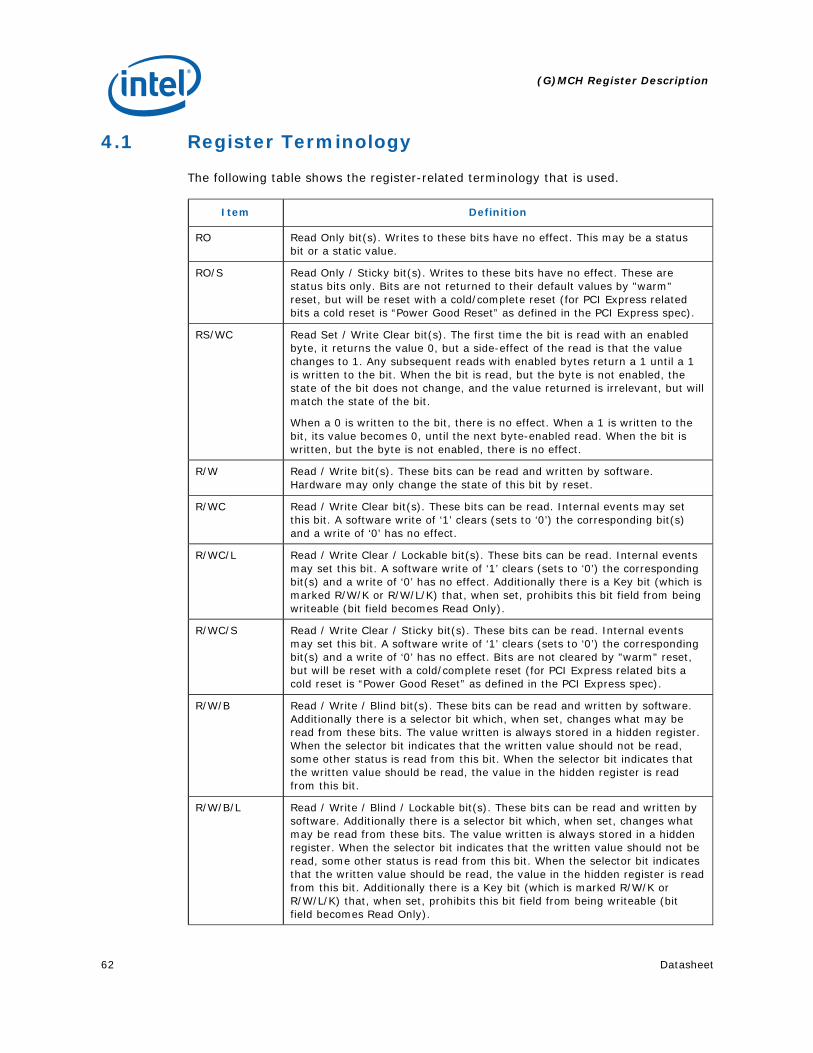
4.1 Register Terminology ............................................................................62 4.2 Configuration Process and Registers........................................................64
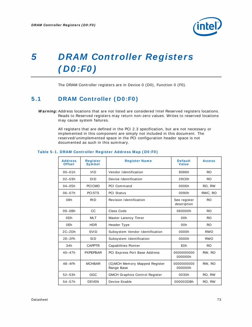
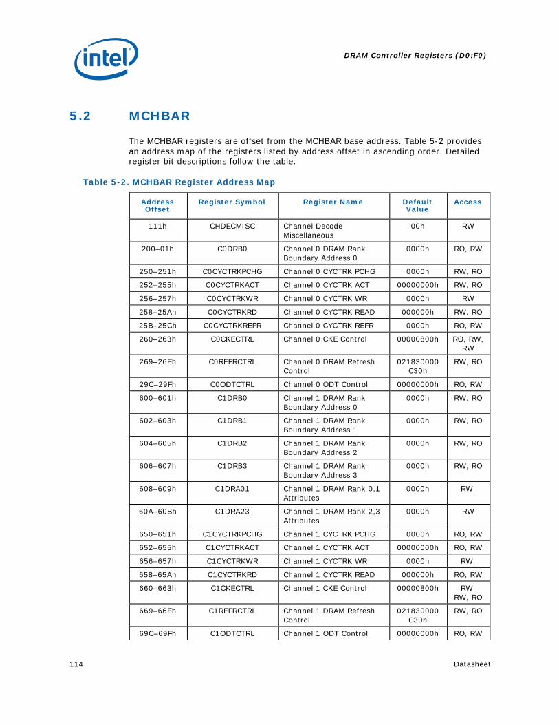
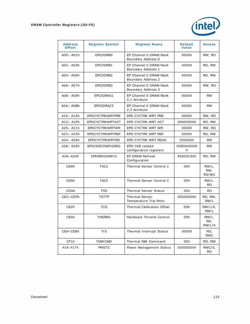
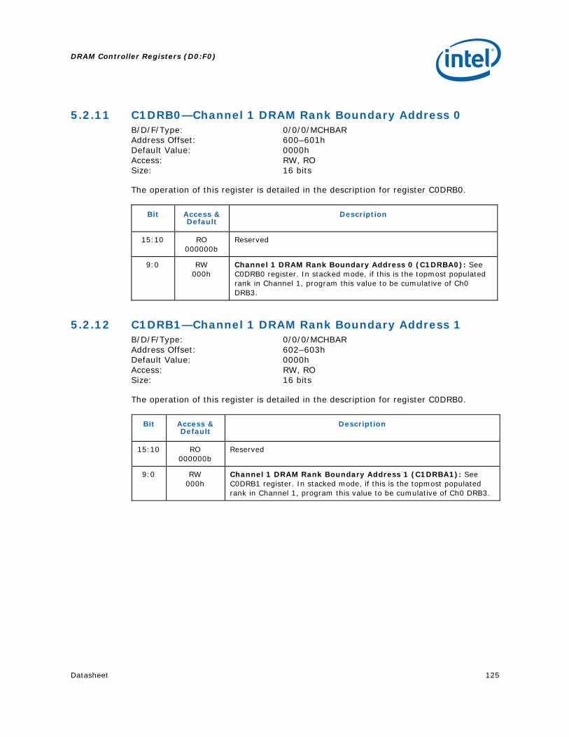
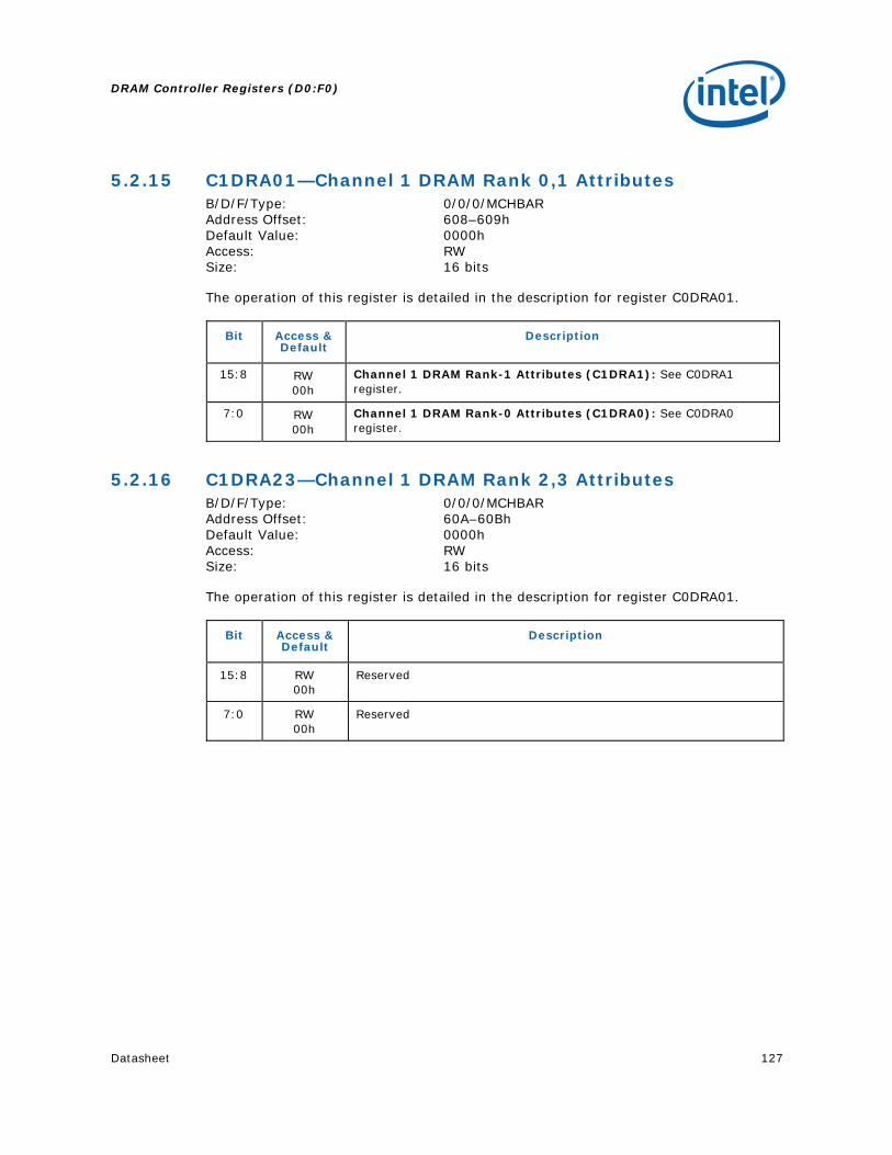
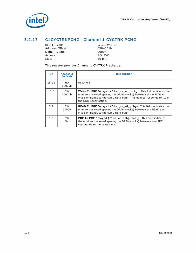
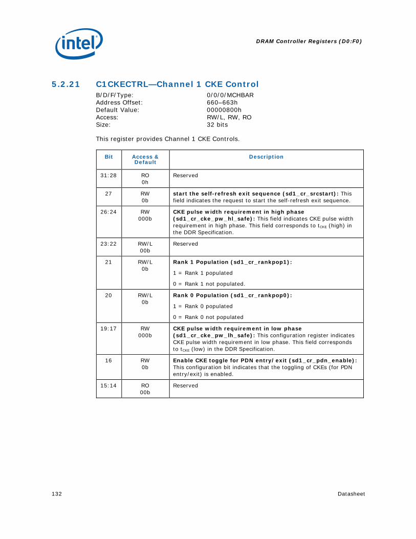
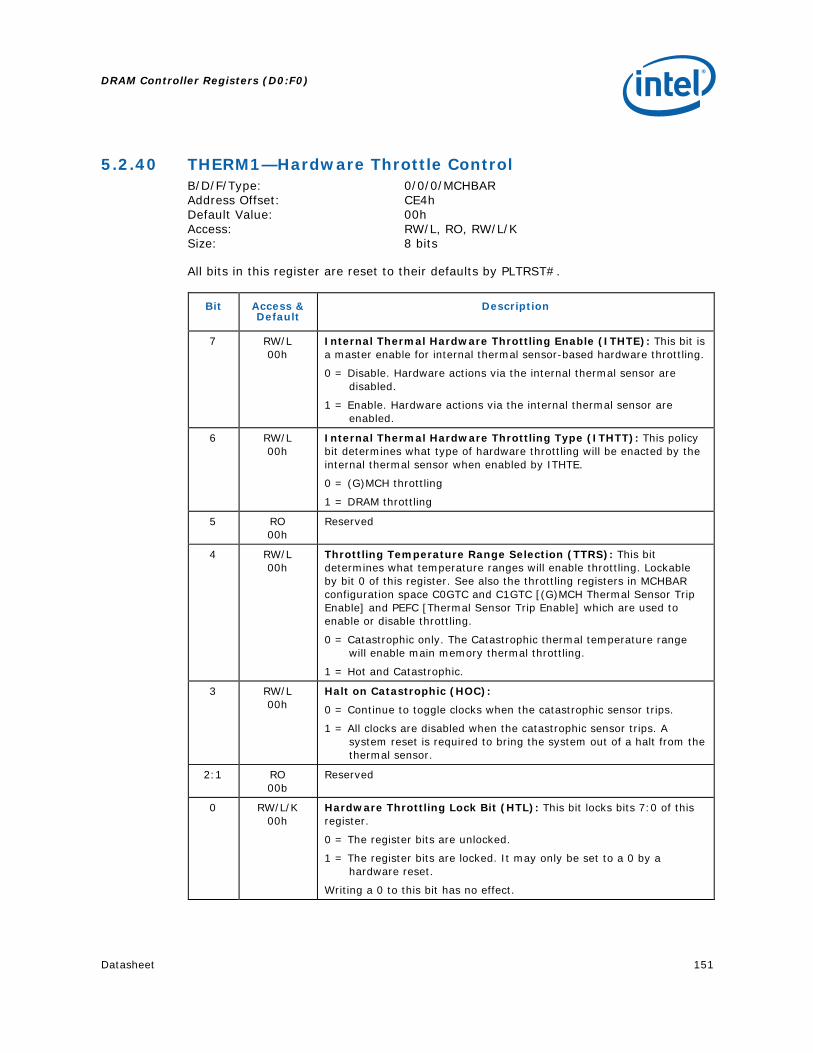
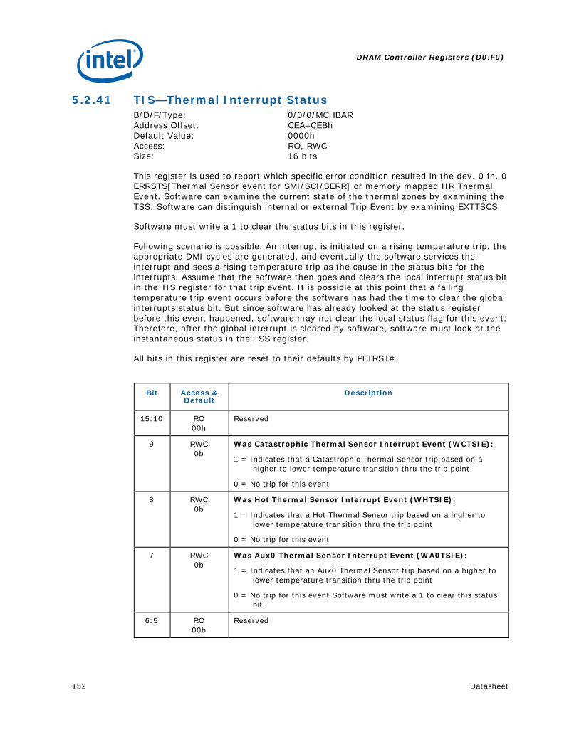
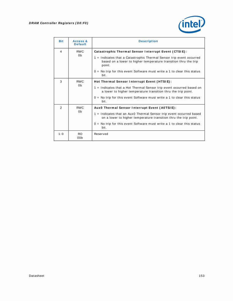
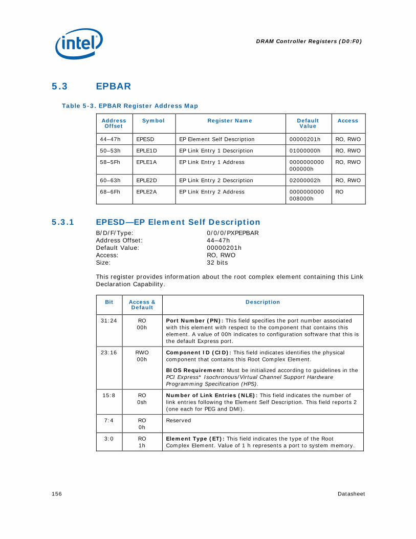
5 DRAM Controller Registers (D0:F0)....................................................................73 5.1 DRAM Controller (D0:F0).......................................................................73
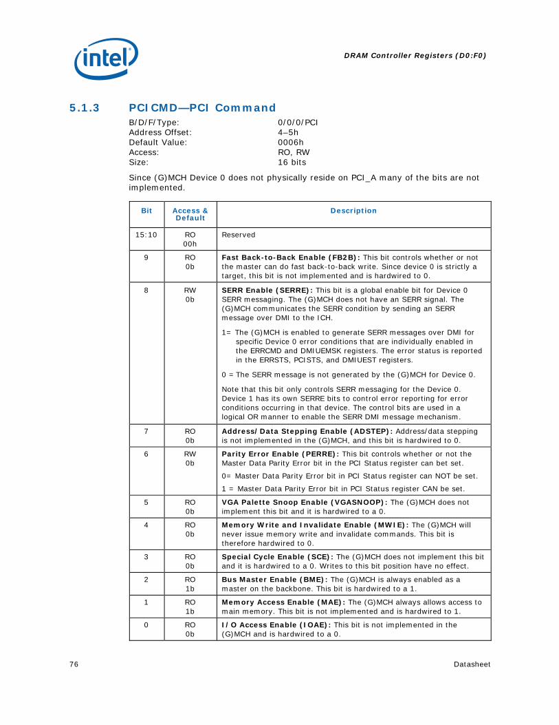
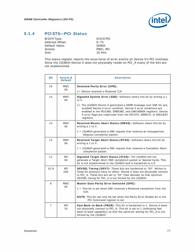
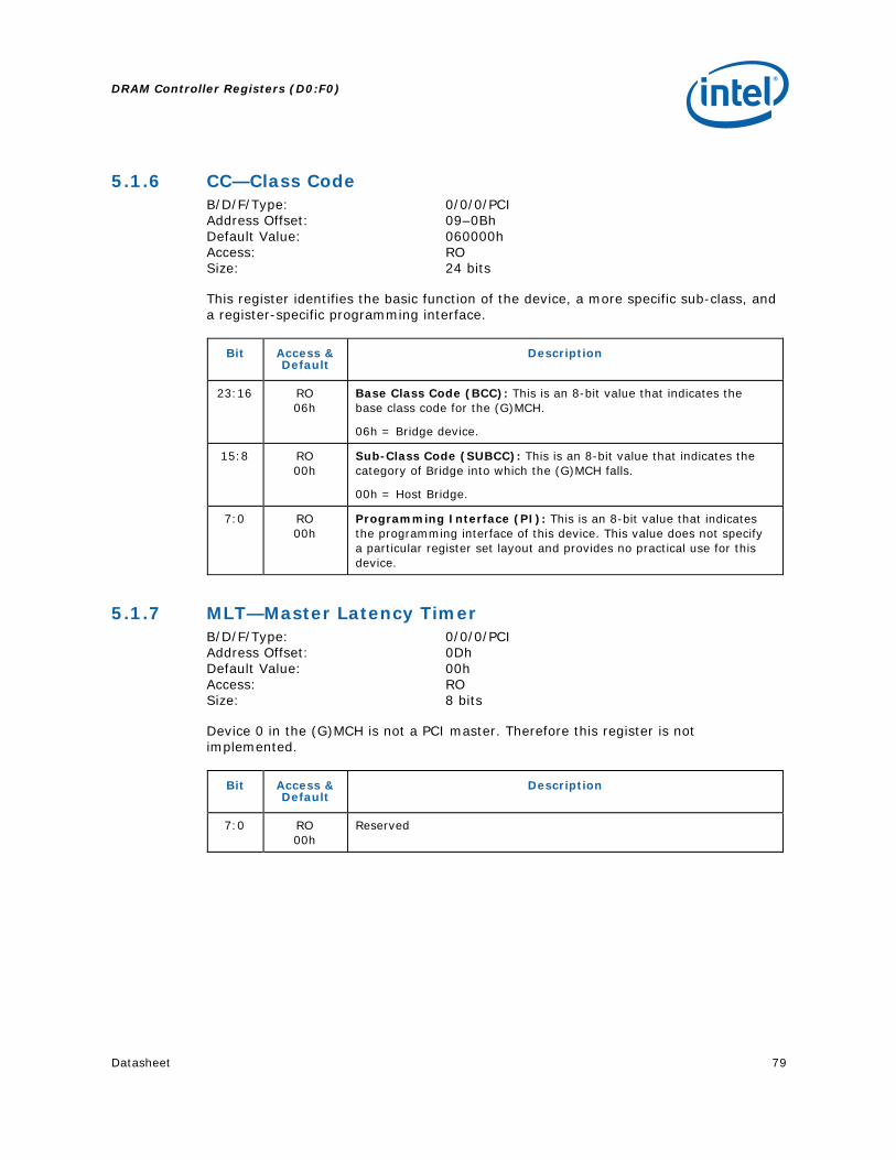
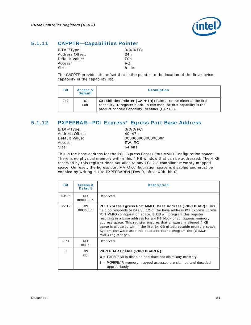
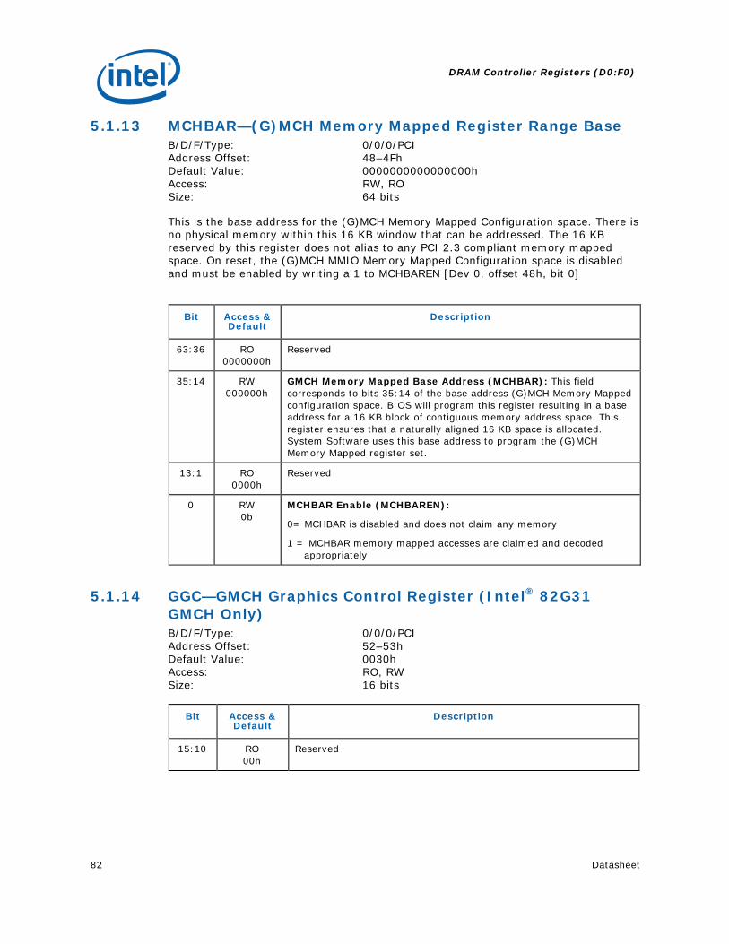
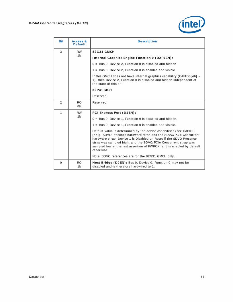
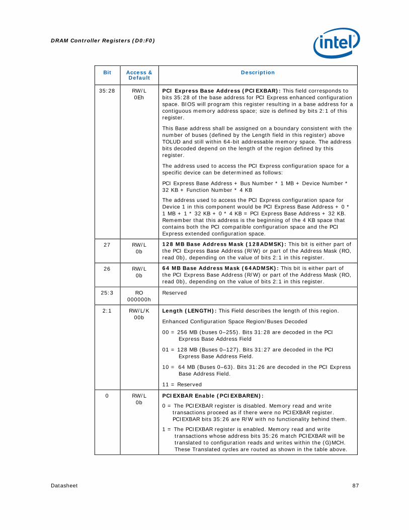
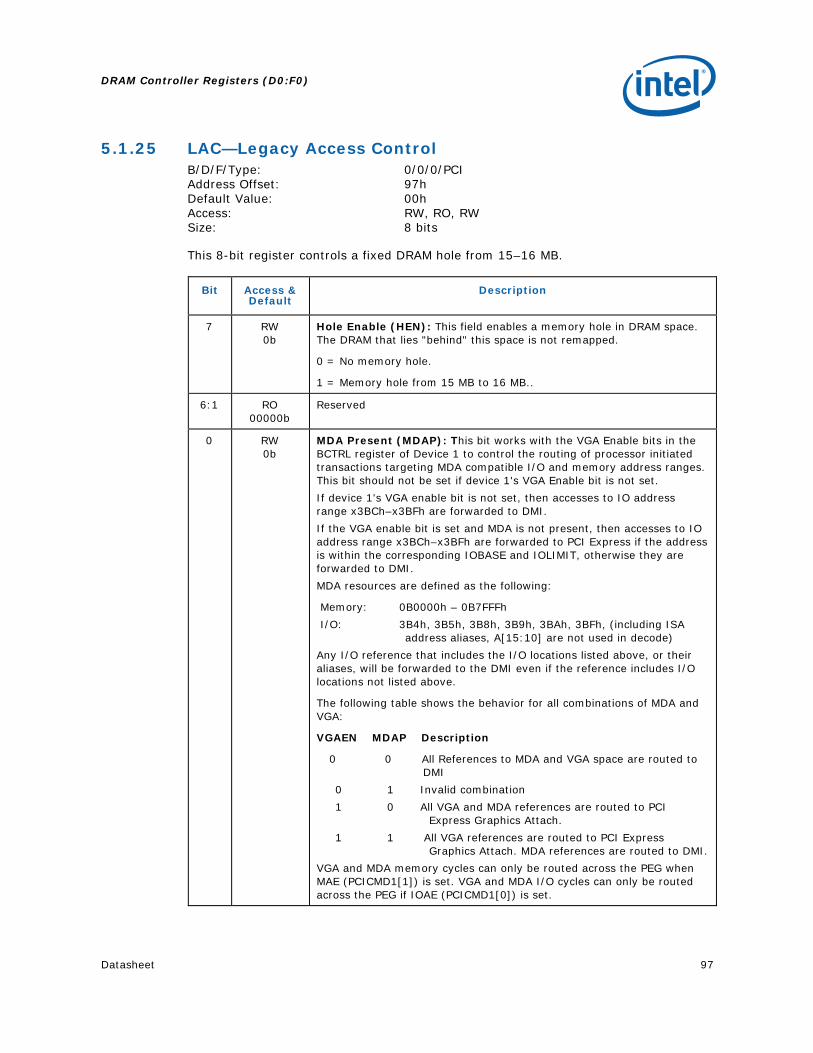
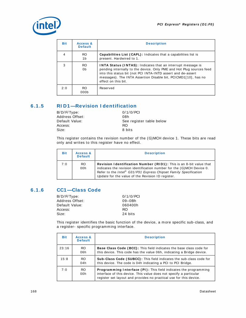
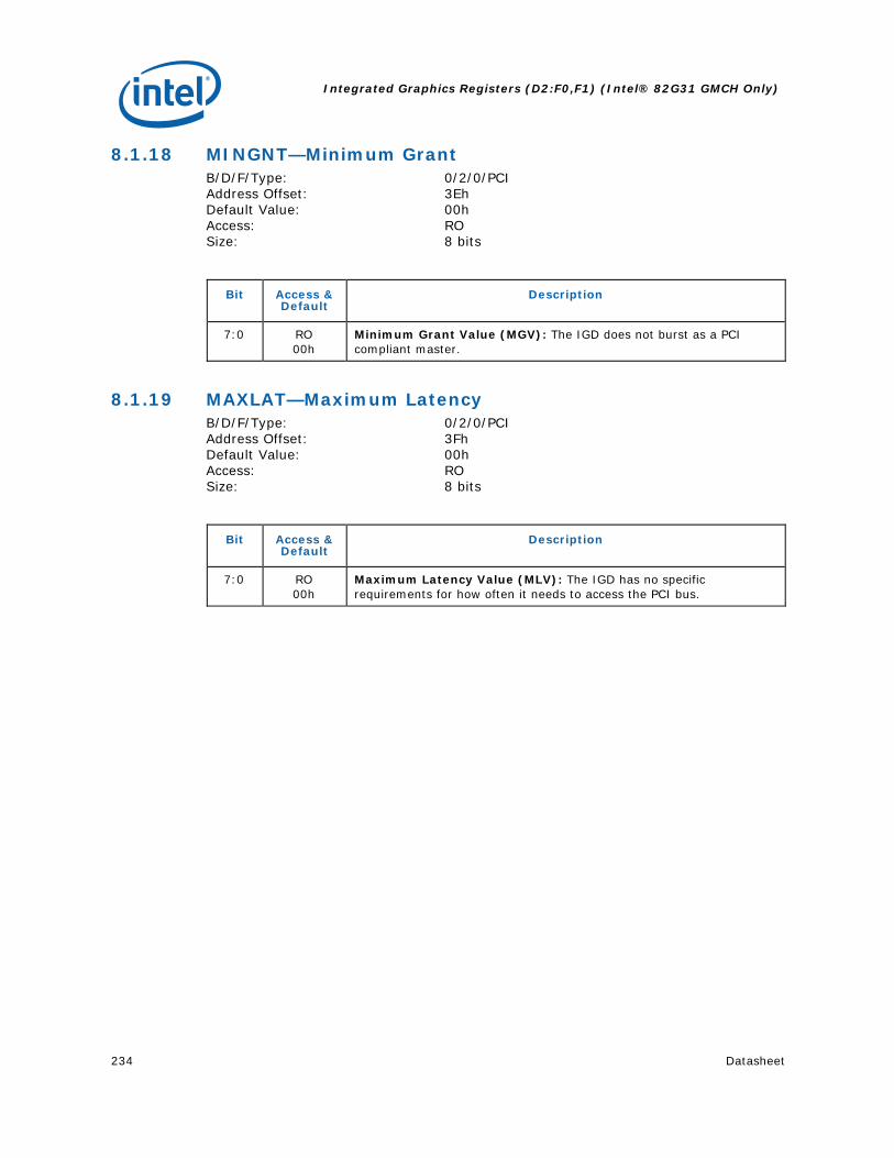
5.1.1 VID—Vendor Identification........................................................75 5.1.2 DID—Device Identification ........................................................75 5.1.3 PCICMD—PCI Command...........................................................76 5.1.4 PCISTS—PCI Status.................................................................77 5.1.5 RID—Revision Identification......................................................78 5.1.6 CC—Class Code.......................................................................79 5.1.7 MLT—Master Latency Timer ......................................................79 5.1.8 HDR—Header Type ..................................................................80 5.1.9 SVID—Subsystem Vendor Identification......................................80 5.1.10 SID—Subsystem Identification ..................................................80 5.1.11 CAPPTR—Capabilities Pointer ....................................................81 5.1.12 PXPEPBAR—PCI Express* Egress Port Base Address .....................81 5.1.13 MCHBAR—(G)MCH Memory Mapped Register Range Base ..............82 5.1.14 GGC—GMCH Graphics Control Register (Intel® 82G31 GMCH Only).82 5.1.15 DEVEN—Device Enable.............................................................84 5.1.16 PCIEXBAR—PCI Express* Register Range Base Address ................86 5.1.17 DMIBAR—Root Complex Register Range Base Address ..................88
Datasheet 5
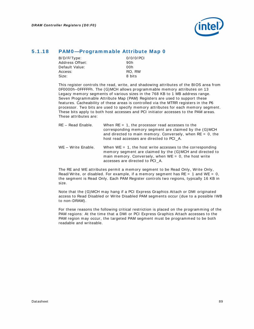
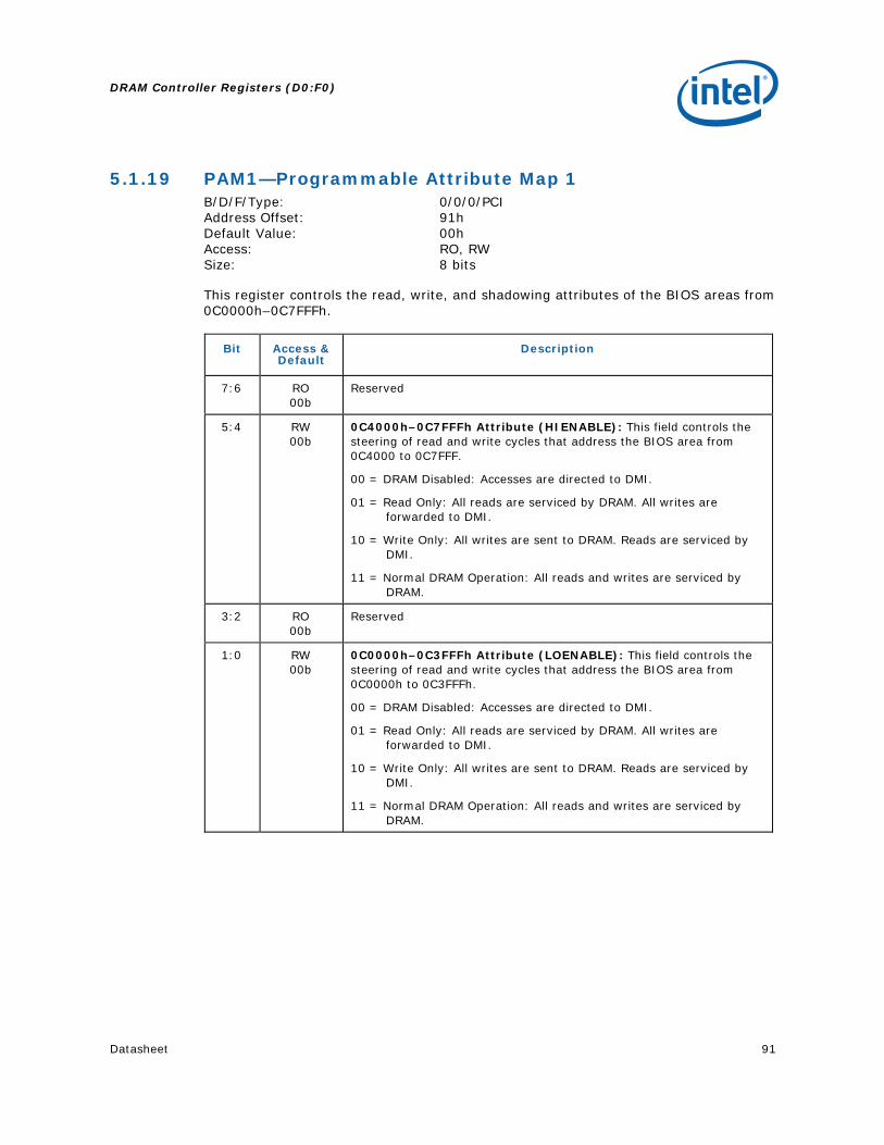
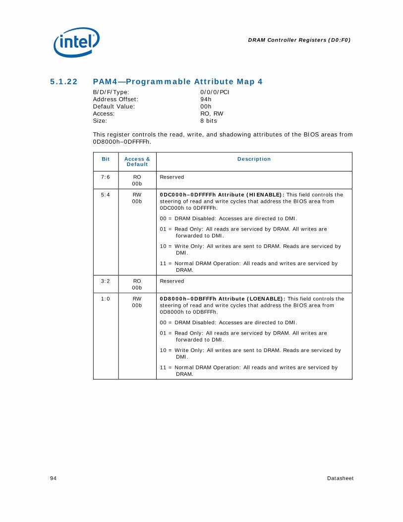
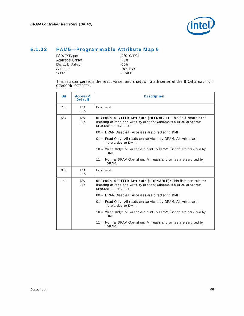
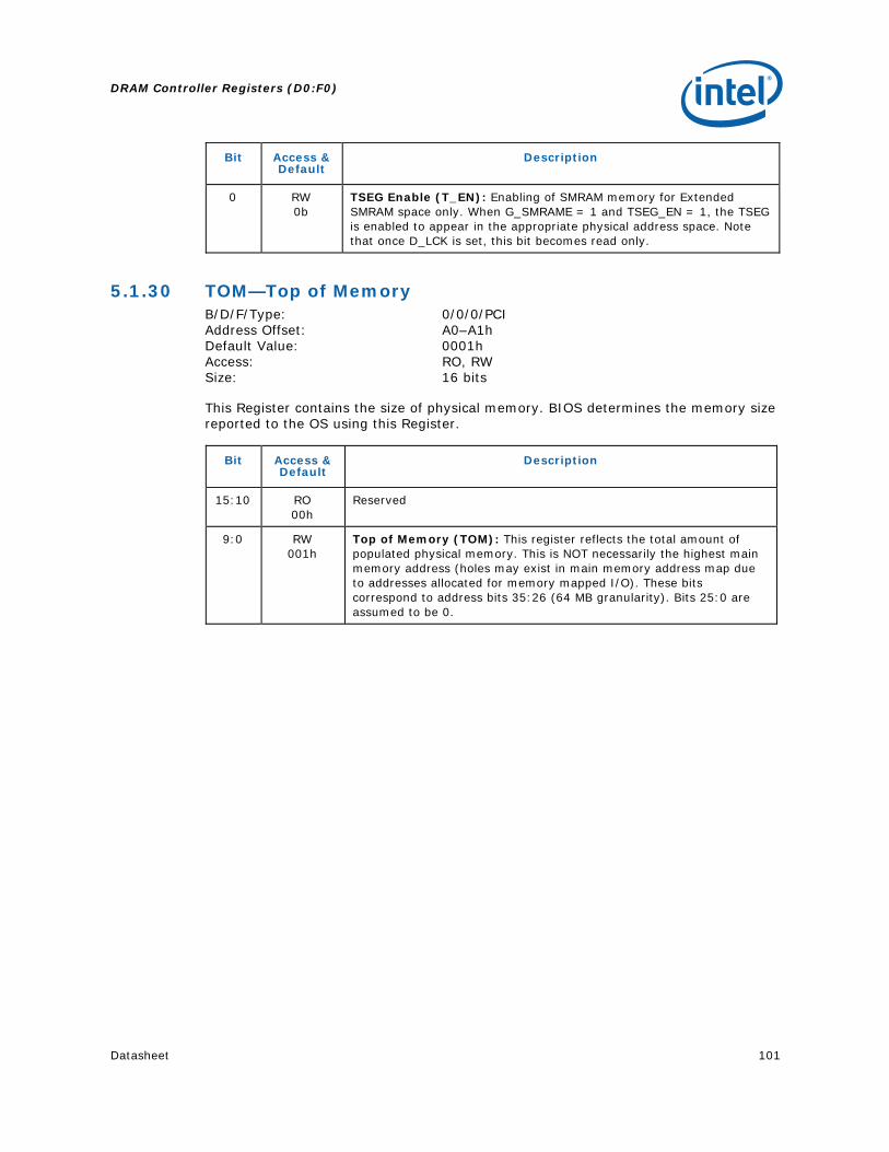
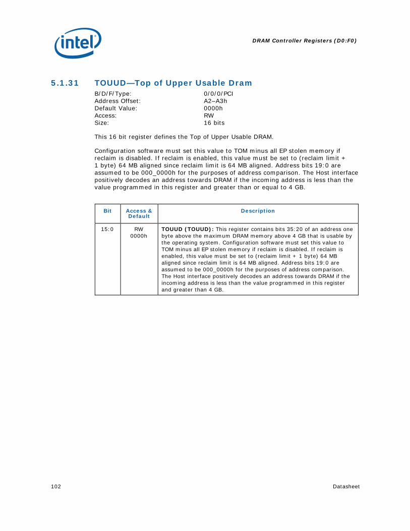
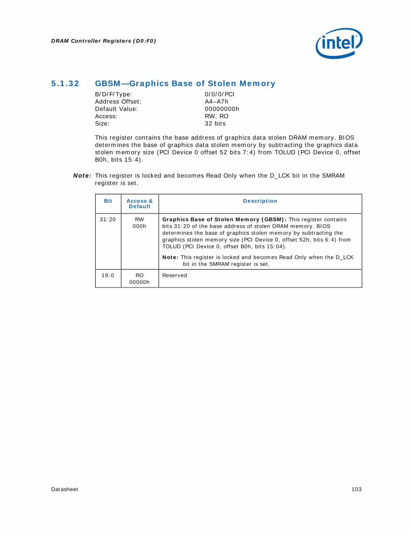
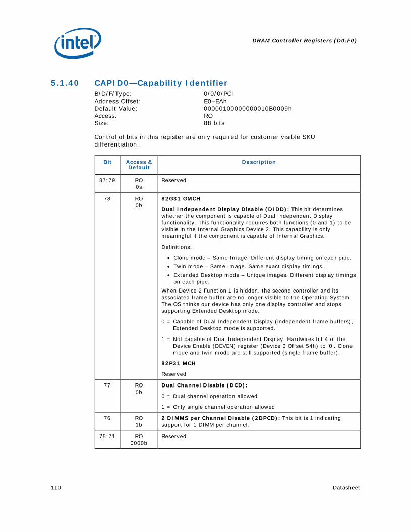
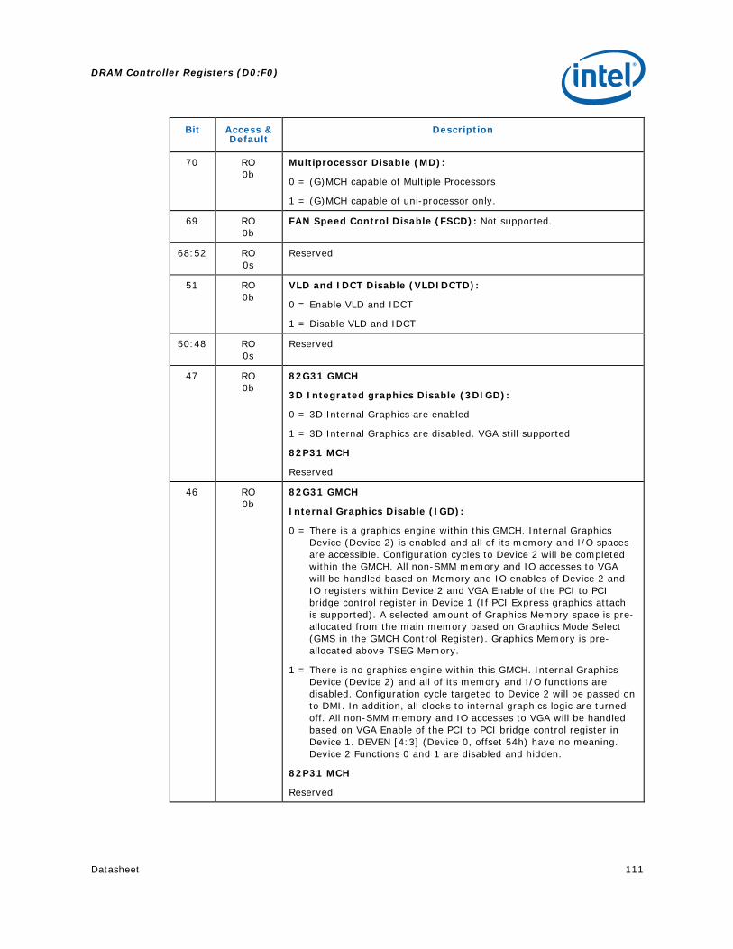
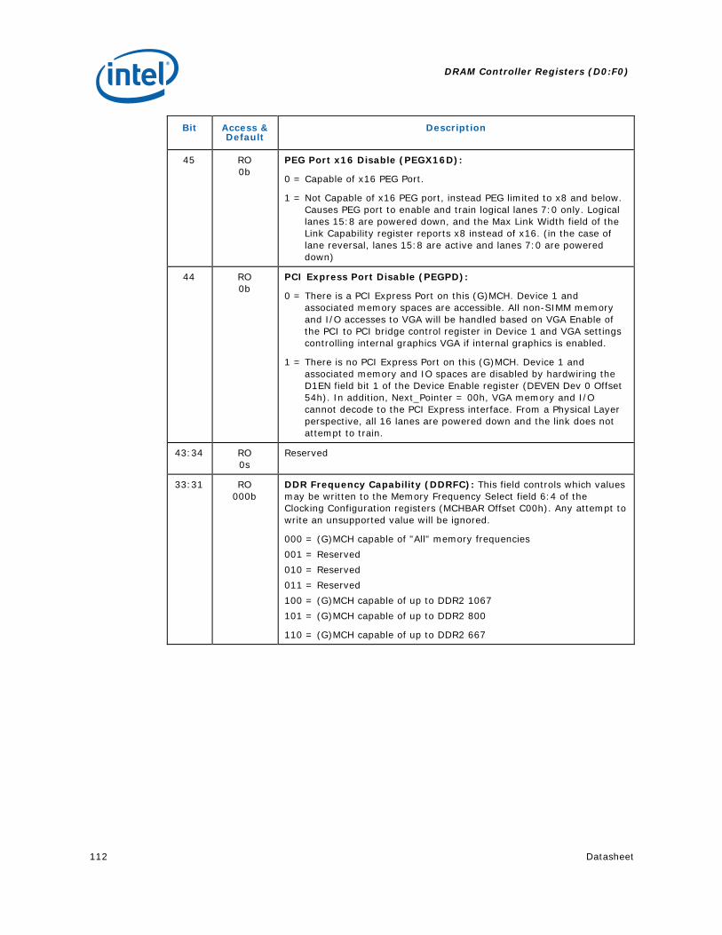
5.1.18 PAM0—Programmable Attribute Map 0........................................89 5.1.19 PAM1—Programmable Attribute Map 1........................................91 5.1.20 PAM2—Programmable Attribute Map 2........................................92 5.1.21 PAM3—Programmable Attribute Map 3........................................93 5.1.22 PAM4—Programmable Attribute Map 4........................................94 5.1.23 PAM5—Programmable Attribute Map 5........................................95 5.1.24 PAM6—Programmable Attribute Map 6........................................96 5.1.25 LAC—Legacy Access Control......................................................97 5.1.26 REMAPBASE—Remap Base Address Register................................98 5.1.27 REMAPLIMIT—Remap Limit Address Register ...............................98 5.1.28 SMRAM—System Management RAM Control ................................99 5.1.29 ESMRAMC—Extended System Management RAM Control ............. 100 5.1.30 TOM—Top of Memory............................................................. 101 5.1.31 TOUUD—Top of Upper Usable Dram ......................................... 102 5.1.32 GBSM—Graphics Base of Stolen Memory................................... 103 5.1.33 BGSM—Base of GTT stolen Memory.......................................... 104 5.1.34 TSEGMB—TSEG Memory Base ................................................. 104 5.1.35 TOLUD—Top of Low Usable DRAM............................................ 105 5.1.36 ERRSTS—Error Status............................................................ 106 5.1.37 ERRCMD—Error Command...................................................... 108 5.1.38 SMICMD—SMI Command........................................................ 109 5.1.39 SKPD—Scratchpad Data ......................................................... 109 5.1.40 CAPID0—Capability Identifier .................................................. 110
9.1.4 FSB Dynamic Bus Inversion .................................................... 267 9.1.5 APIC Cluster Mode Support ..................................................... 268
9.2 System Memory Controller................................................................... 268 9.2.1 System Memory Organization Modes ........................................ 268 9.2.2 System Memory Technology Supported .................................... 270
9.3 PCI Express* ..................................................................................... 271 9.3.1 Intel® Serial Digital Video Output (sDVO)
10.1 Absolute Minimum and Maximum Ratings .............................................. 287 10.1.1 Current Consumption............................................................. 289
10.2 Signal Groups .................................................................................... 291 10.3 Buffer Supply and DC Characteristics .................................................... 294
10.3.1 I/O Buffer Supply Voltages ..................................................... 294 10.3.2 General DC Characteristics ..................................................... 296
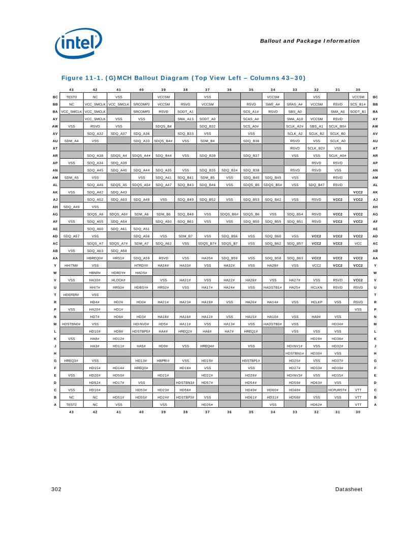
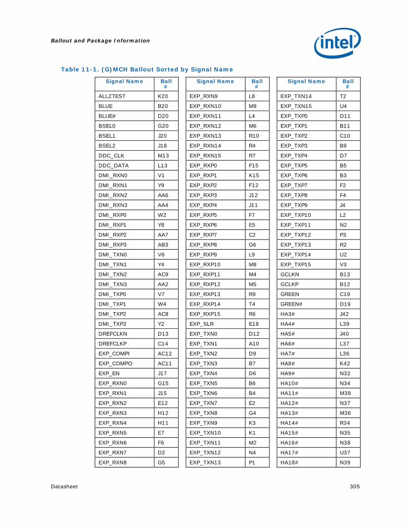
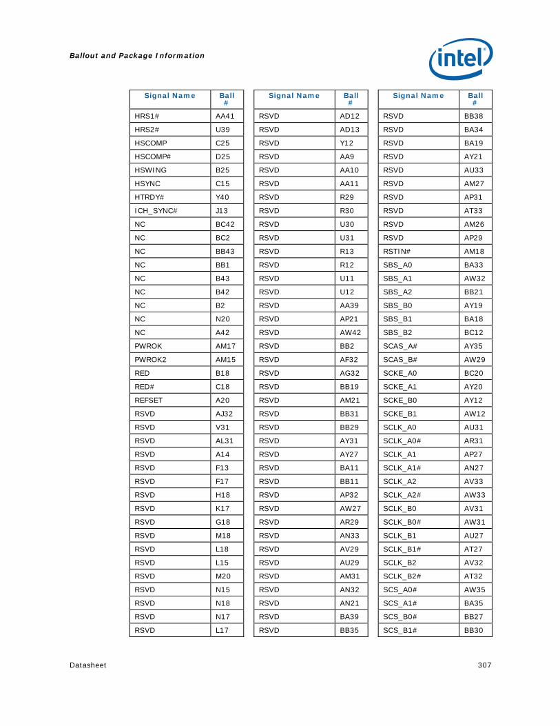
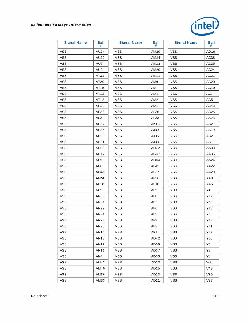
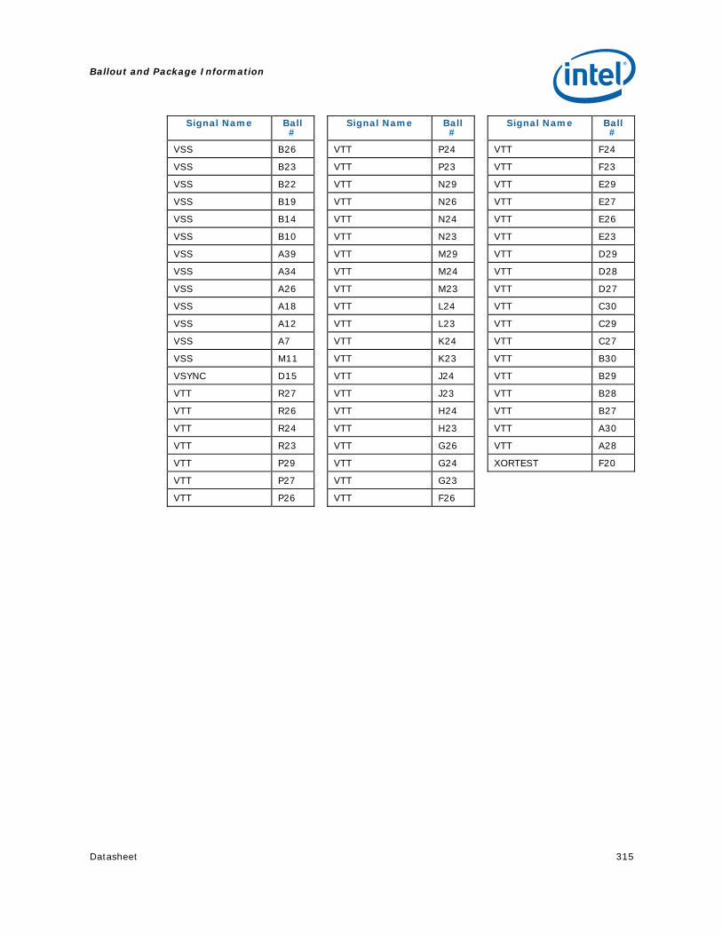
10.4 R, G, B / CRT DAC Display DC Characteristics (Intel® 82G31 GMCH Only)... 300 11 Ballout and Package Information ..................................................................... 301
Table 3-1. Expansion Area Memory Segments .....................................................46 Table 3-2. Extended System BIOS Area Memory Segments ...................................47 Table 3-3. System BIOS Area Memory Segments.................................................47 Table 3-4. Pre-allocated Memory Example for 64 MB DRAM, 1 MB VGA, 1 MB
GTT stolen and 1 MB TSEG ................................................................49 Table 3-5. Pre-Allocated Memory Example for 64-MB DRAM, 1-MB VGA and
• System Memory Interface ⎯ One or two channels (each channel consisting of 64
data lines) ⎯ Single or Dual Channel memory organization ⎯ DDR2-800/667 frequencies ⎯ Unbuffered, non-ECC DIMMs only ⎯ Supports 1-Gb, 512-Mb DDR2 technologies for x8
and x16 devices ⎯ 4 GB maximum memory
• Direct Media Interface (DMI) ⎯ Chip-to-chip connection interface to Intel ICH7 ⎯ 2 GB/s point-to-point DMI to ICH9 (1 GB/s each
direction) ⎯ 100 MHz reference clock (shared with PCI Express
• PCI Express* Interface ⎯ One x16 PCI Express port ⎯ Compatible with the PCI Express Base Specification,
Revision 1.1 ⎯ Raw bit rate on data pins of 2.5 Gb/s resulting in a
real bandwidth per pair of 250 MB/s
• Integrated Graphics Device (82G31 GMCH only) ⎯ Core frequency of 400 MHz ⎯ 1.6 GP/s pixel rate ⎯ High-Quality 3D Setup and Render Engine ⎯ High-Quality Texture Engine ⎯ 3D Graphics Rendering Enhancements ⎯ 2D Graphics ⎯ Video Overlay ⎯ Multiple Overlay Functionality
• Analog Display (82G31 GMCH only) ⎯ 350 MHz Integrated 24-bit RAMDAC ⎯ Up to 2048x1536 @ 75 Hz refresh ⎯ Hardware Color Cursor Support ⎯ DDC2B Compliant Interface
• Digital Display (82G31 GMCH only) ⎯ SDVO ports in single mode supported ⎯ 225 MHz dot clock on each 12-bit interface ⎯ Flat panels up to 1920x1200 @ 60 Hz or
digital CRT/HDTV at 1400x1050 @ 85Hz ⎯ Dual independent display options with
digital display ⎯ Multiplexed digital display channels
(supported with ADD2 Card). ⎯ Supports TMDS transmitters or TV-Out
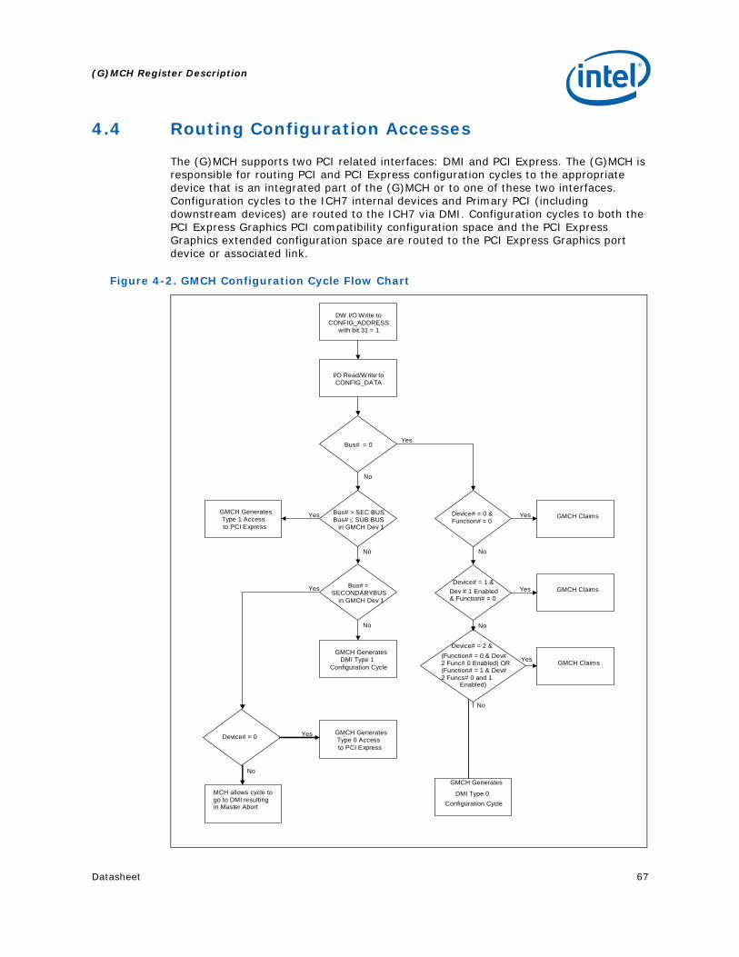
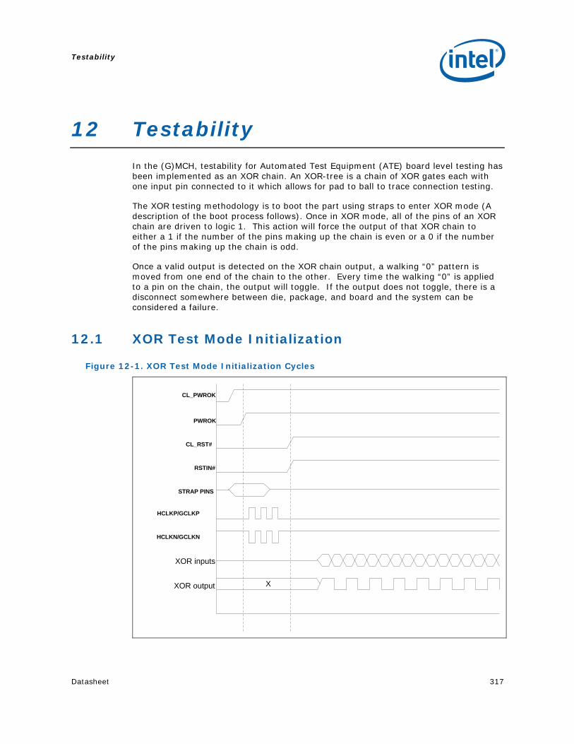
1 Introduction The Intel® G31/P31 Express Chipset is designed for use with Intel® Core™2 Duo desktop processor and Intel® Core™2 Quad processor based platforms. The chipsets each contain two components: GMCH (or MCH) for the host bridge and I/O Controller Hub 7 (ICH7) for the I/O subsystem. The 82G31 GMCH is part of the Intel® G31 Express Chipset. The 82P31 MCH is part of the Intel® P31 Express chipset. The ICH7 is the seventh generation I/O Controller Hub and provides a multitude of I/O related functions. Figure 1-1 and Figure 1-2 show examples system block diagrams for the Intel® G31 and P31 Express Chipsets.
This document is the datasheet for the Intel® 82G31 Graphics and Memory Controller Hub (GMCH) and Intel® 82P31 Memory Controller Hub (MCH). Topics covered include; signal description, system memory map, PCI register description, a description of the (G)MCH interfaces and major functional units, electrical characteristics, ballout definitions, and package characteristics.
The primary difference between the Intel® 82G31 GMCH and 82P31 MCH is that the 82G31 GMCH has an integrated graphics device (IGD) plus the associated display interfaces. The 82P31 does not contain an IGD and the associated interfaces.
Note: Unless otherwise specified, the information in this document applies to the Intel® 82G31 Graphics and Memory Controller Hub (GMCH) and Intel® 82P31 Memory Controller Hub (MCH).
Note: The term (G)MCH refers to the 82G31 GMCH and 82P31 MCH.
Note: Unless otherwise specified, ICH7 refers to the Intel® 82801GB ICH7, Intel® 82801GR ICH7R, and Intel® 82801GDH ICH7DH I/O Controller Hub 7 components.
Introduction
16 Datasheet
Figure 1-1. Intel® G31 Express Chipset System Block Diagram Example
Processor
GMCH DDR2
DDR2
Channel A
800/1066 MHz FSB
DMI Interface
Channel B
System Memory
Display Add2Card
SDVO
OR
PCI Express* X16 Graphics
VGA
Analog Display
Intel®
ICH 7
USB* 2.08 ports, 480 Mb/s
4 SATA* Ports
IDE
Super I/O
PCI Bus
AC '97/ Intel® High Definition Audio
CODECs
LPC Interface
Power Management
Clock Generation
System Management (TCO )
LAN Connect
SMBus 2.0/I2 C
GPIO
PCI Express* x1
Intel® PCI Express Gigabit Ethernet
SPI BIOS
TPM(Optional) Flash BIOS
PATA
6
(1 DIMM per Channel)
Graphics Card
Display
Intel® G31 Express Chipset
Introduction
Datasheet 17
Figure 1-2. Intel® P31 Express Chipset System Block Diagram Example
Processor
MCH DDR2
DDR2
Channel A
800/1066 MHz FSB
DMI Interface
Channel B
System Memory
Intel®
ICH 7
USB* 2.08 ports, 480 Mb/s
4 SATA* Ports
IDE
Super I/O
PCI Bus
AC '97/ Intel® High Definition Audio
CODECs
LPC Interface
Power Management
Clock Generation
System Management (TCO )
LAN Connect
SMBus 2.0/I2 C
GPIO
PCI Express* x1
Intel® PCI Express Gigabit Ethernet
SPI BIOS
TPM(Optional) Flash BIOS
PATA
6
(1 DIMM per Channel)
PCI Express* X16 Graphics
Graphics Card
Display
Intel® P31 Express Chipset
Introduction
18 Datasheet
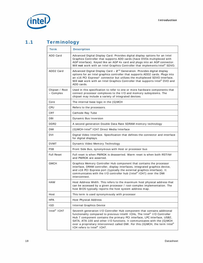
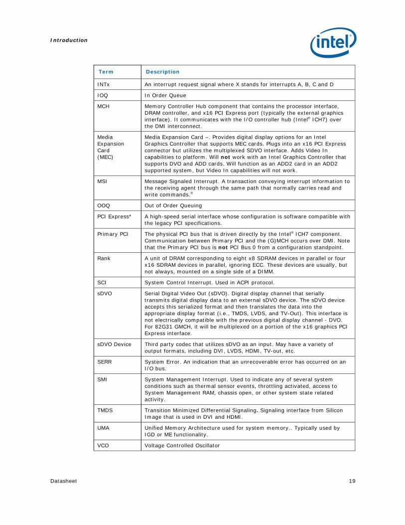
1.1 Terminology Term Description
ADD Card Advanced Digital Display Card. Provides digital display options for an Intel Graphics Controller that supports ADD cards (have DVOs multiplexed with AGP interface). Keyed like an AGP 4x card and plugs into an AGP connector. Will not work with an Intel Graphics Controller that implements Intel® SDVO.
ADD2 Card Advanced Digital Display Card – 2nd Generation. Provides digital display options for an Intel graphics controller that supports ADD2 cards. Plugs into an x16 PCI Express* connector but utilizes the multiplexed SDVO interface. Will not work with an Intel Graphics Controller that supports Intel® DVO and ADD cards.
Chipset / Root – Complex
Used in this specification to refer to one or more hardware components that connect processor complexes to the I/O and memory subsystems. The chipset may include a variety of integrated devices.
Core The internal base logic in the (G)MCH
CPU Refers to the processors.
CRT Cathode Ray Tube
DBI Dynamic Bus Inversion
DDR2 A second generation Double Data Rate SDRAM memory technology
DMI (G)MCH-Intel® ICH7 Direct Media Interface
DVI Digital Video Interface. Specification that defines the connector and interface for digital displays.
DVMT Dynamic Video Memory Technology
FSB Front Side Bus, synonymous with Host or processor bus
Full Reset Full reset is when PWROK is deasserted. Warm reset is when both RSTIN# and PWROK are asserted.
GMCH Graphics Memory Controller Hub component that contains the processor interface, DRAM controller, display interfaces, integrated graphics device, and x16 PCI Express port (typically the external graphics interface). It communicates with the I/O controller hub (Intel® ICH7) over the DMI interconnect.
HAW Host Address Width. This refers to the maximum host physical address that can be accessed by a given processor / root-complex implementation. The host BIOS typically reports the host system address map.
Host This term is used synonymously with processor
HPA Host Physical Address
IGD Internal Graphics Device
Intel® ICH7 Seventh generation I/O Controller Hub component that contains additional functionality compared to previous Intel® ICHs, The Intel® I/O Controller Hub 7 component contains the primary PCI interface, LPC interface, USB2, SATA, ATA-100 and other I/O functions. It communicates with the (G)MCH over a proprietary interconnect called DMI. For this (G)MCH, the term Intel® ICH refers to Intel® ICH7.
Introduction
Datasheet 19
Term Description
INTx An interrupt request signal where X stands for interrupts A, B, C and D
IOQ In Order Queue
MCH Memory Controller Hub component that contains the processor interface, DRAM controller, and x16 PCI Express port (typically the external graphics interface). It communicates with the I/O controller hub (Intel® ICH7) over the DMI interconnect.
Media Expansion Card (MEC)
Media Expansion Card –. Provides digital display options for an Intel Graphics Controller that supports MEC cards. Plugs into an x16 PCI Express connector but utilizes the multiplexed SDVO interface. Adds Video In capabilities to platform. Will not work with an Intel Graphics Controller that supports DVO and ADD cards. Will function as an ADD2 card in an ADD2 supported system, but Video In capabilities will not work.
MSI Message Signaled Interrupt. A transaction conveying interrupt information to the receiving agent through the same path that normally carries read and write commands.®
OOQ Out of Order Queuing
PCI Express* A high-speed serial interface whose configuration is software compatible with the legacy PCI specifications.
Primary PCI The physical PCI bus that is driven directly by the Intel® ICH7 component. Communication between Primary PCI and the (G)MCH occurs over DMI. Note that the Primary PCI bus is not PCI Bus 0 from a configuration standpoint.
Rank A unit of DRAM corresponding to eight x8 SDRAM devices in parallel or four x16 SDRAM devices in parallel, ignoring ECC. These devices are usually, but not always, mounted on a single side of a DIMM.
SCI System Control Interrupt. Used in ACPI protocol.
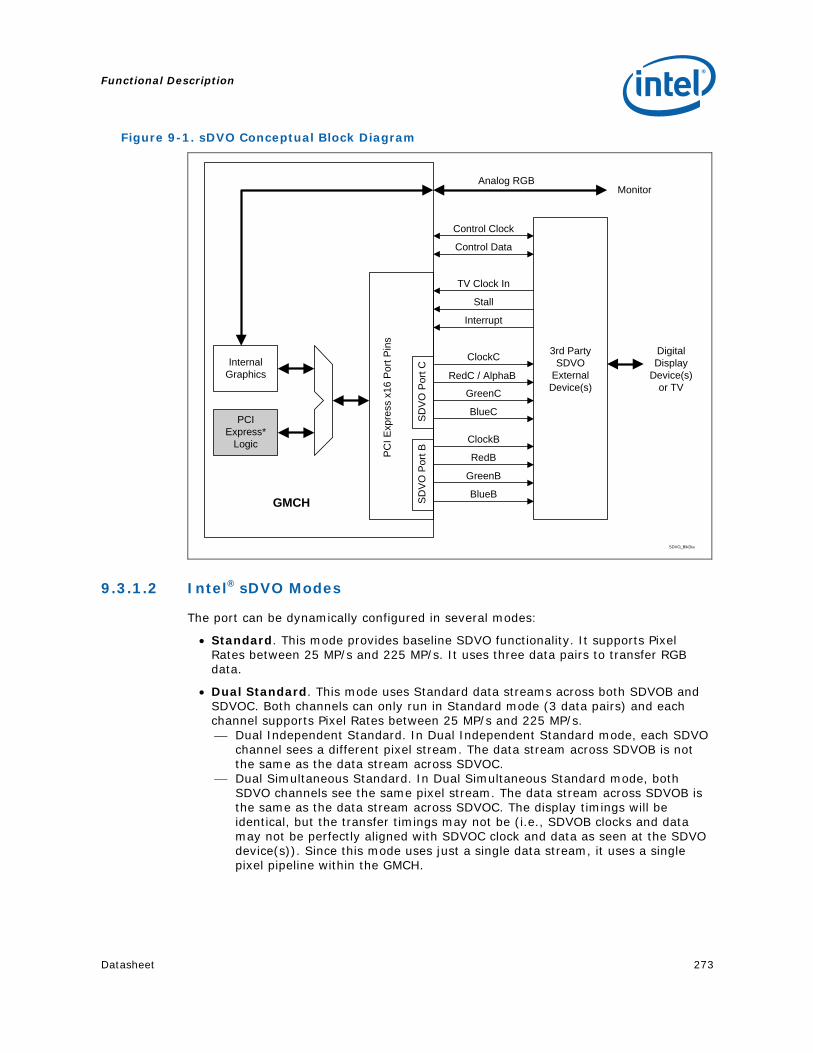
sDVO Serial Digital Video Out (sDVO). Digital display channel that serially transmits digital display data to an external sDVO device. The sDVO device accepts this serialized format and then translates the data into the appropriate display format (i.e., TMDS, LVDS, and TV-Out). This interface is not electrically compatible with the previous digital display channel - DVO. For 82G31 GMCH, it will be multiplexed on a portion of the x16 graphics PCI Express interface.
sDVO Device Third party codec that utilizes sDVO as an input. May have a variety of output formats, including DVI, LVDS, HDMI, TV-out, etc.
SERR System Error. An indication that an unrecoverable error has occurred on an I/O bus.
SMI System Management Interrupt. Used to indicate any of several system conditions such as thermal sensor events, throttling activated, access to System Management RAM, chassis open, or other system state related activity.
TMDS Transition Minimized Differential Signaling. Signaling interface from Silicon Image that is used in DVI and HDMI.
UMA Unified Memory Architecture used for system memory.. Typically used by IGD or ME functionality.
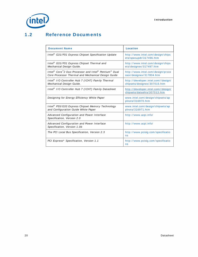
Intel® I/O Controller Hub 7 (ICH7) Family Datasheet http://developer.intel.com//design/chipsets/datashts/307013.htm
Designing for Energy Efficiency White Paper www.intel.com/design/chipsets/applnots/316970.htm
Intel® P35/G33 Express Chipset Memory Technology and Configuration Guide White Paper
www.intel.com/design/chipsets/applnots/316971.htm
Advanced Configuration and Power Interface Specification, Version 2.0
http://www.acpi.info/
Advanced Configuration and Power Interface Specification, Version 1.0b
http://www.acpi.info/
The PCI Local Bus Specification, Version 2.3 http://www.pcisig.com/specifications
PCI Express* Specification, Version 1.1 http://www.pcisig.com/specifications
Introduction
Datasheet 21
1.3 (G)MCH Overview
The Intel® 82G31 GMCH and 82P31 MCH are designed for use with the Intel® Core™2 Duo processors and Intel® Core™2 Quad processors in desktop platforms. The role of a (G)MCH in a system is to manage the flow of information between its four interfaces: the processor interface, the system memory interface, the external graphics interface, and the I/O controller through DMI interface. This includes arbitrating between the four interfaces when each initiates transactions. The (G)MCH supports one or two channels of DDR2 SDRAM. It also supports the PCI Express based external graphics attach. The Intel® G31/P31 platform supports the seventh generation I/O Controller Hub (Intel® ICH7).
1.3.1 Host Interface
The (G)MCH can use a single LGA775 socket processor. The (G)MCH supports a FSB frequency of 800/1066 MHz. Host-initiated I/O cycles are decoded to PCI Express, DMI, or the (G)MCH configuration space. Host-initiated memory cycles are decoded to PCI Express, DMI or system memory. PCI Express device accesses to non-cacheable system memory are not snooped on the host bus. Memory accesses initiated from PCI Express using PCI semantics and from DMI to system SDRAM will be snooped on the host bus.
Capabilities of the Host Interface include:
• Supports Intel CoreTM2 Duo processors and Intel® Core™2 Quad processors
• Supports Front Side Bus (FSB) at the following Frequency Ranges: ⎯ 800/1066 (200/266MHz)
• Supports FSB Dynamic Bus Inversion (DBI)
• Supports 36-bit host bus addressing, allowing the processor to access the entire 64 GB of the host address space.
• Has a 12-deep In-Order Queue to support up to twelve outstanding pipelined address requests on the host bus
• Has a 1-deep Defer Queue
• Uses GTL+ bus driver with integrated GTL termination resistors
• Supports a Cache Line Size of 64 bytes
Introduction
22 Datasheet
1.3.2 System Memory Interface The (G)MCH integrates a system memory DDR2 controller with two, 64-bit wide interfaces. The buffers support SSTL_1.8 (Stub Series Terminated Logic for 1.8 V) signal interfaces. The memory controller interface is fully configurable through a set of control registers.
Capabilities of the system memory interface include:
• Directly supports one or two channels of DDR2 memory with a maximum of one DIMM per channel
• Supports single and dual channel memory organization modes
• Supports a data burst length of eight for all memory organization modes
• Supports memory data transfer rates of 667 and 800 MHz for DDR2
• I/O Voltage of 1.8 V for DDR2
• Supports only un-buffered non-ECC DDR2 DIMMs
• Supports maximum memory bandwidth of 6.4 GB/s in single-channel or dual-channel asymmetric mode, or 12.8 GB/s in dual-channel symmetric mode assuming DDR2 800MHz
• Supports 512 Mb and 1 Gb DDR2 DRAM technologies for x8 and x16 devices
• Using 512 Mb device technologies, the smallest memory capacity possible is 256 MB, assuming Single Channel Mode with a single x16 single sided un-buffered non-ECC DIMM memory configuration
• Using 1 Gb device technologies, the largest memory capacity possible is 4 GB, assuming Dual Channel Mode with two x8 double sided un-buffered non-ECC DIMM memory configuration
• Supports up to 16 simultaneous open pages per channel (assuming 2 ranks of 8 bank devices)
• Supports opportunistic refresh scheme
• Supports Partial Writes to memory using Data Mask (DM) signals
• Supports a memory thermal management scheme to selectively manage reads and/or writes. Memory thermal management can be triggered either by on-die thermal sensor, or by preset limits. Management limits are determined by weighted sum of various commands that are scheduled on the memory interface
Introduction
Datasheet 23
1.3.3 Direct Media Interface (DMI)
Direct Media Interface (DMI) is the chip-to-chip connection between the (G)MCH and ICH7. This high-speed interface integrates advanced priority-based servicing allowing for concurrent traffic and true isochronous transfer capabilities. Base functionality is completely software transparent permitting current and legacy software to operate normally.
To provide for true isochronous transfers and configurable Quality of Service (QoS) transactions, the ICH7 supports two virtual channels on DMI: VC0 and VC1. These two channels provide a fixed arbitration scheme where VC1 is always the highest priority. VC0 is the default conduit of traffic for DMI and is always enabled. VC1 must be specifically enabled and configured at both ends of the DMI link (i.e., the ICH7 and (G)MCH).
• A chip-to-chip connection interface to Intel ICH7
• 2 GB/s point-to-point DMI to ICH7 (1 GB/s each direction)
• APIC and MSI interrupt messaging support. Will send Intel-defined “End Of Interrupt” broadcast message when initiated by the processor.
• Message Signaled Interrupt (MSI) messages
• SMI, SCI and SERR error indication
1.3.4 PCI Express* Interface
The (G)MCH contains one 16-lane (x16) PCI Express port intended for an external PCI Express graphics card. The PCI Express port is compliant to the PCI Express* Base Specification revision 1.1. The x16 port operates at a frequency of 2.5 GB/s on each lane while employing 8b/10b encoding, and supports a maximum theoretical bandwidth of 40 GB/s in each direction. The 82G31 GMCH multiplexes a PCI Express interface with the Intel® sDVO ports.
• One, 16-lane PCI Express port intended for graphics attach, compatible to the PCI Express* Base Specification revision 1.1.
• PCI Express frequency of 1.25 GHz resulting in 2.5 GB/s each direction per lane.
• Raw bit-rate on the data pins of 2.5 GB/s, resulting in a real bandwidth per pair of 250 MB/s given the 8b/10b encoding used to transmit data across this interface
• Maximum theoretical realized bandwidth on the interface of 4 GB/s in each direction simultaneously, for an aggregate of 8 GB/s when x16.
• PCI Express* Graphics Extended Configuration Space. The first 256 bytes of configuration space alias directly to the PCI Compatibility configuration space. The remaining portion of the fixed 4 KB block of memory-mapped space above that (starting at 100h) is known as extended configuration space.
• PCI Express Enhanced Addressing Mechanism. Accessing the device configuration space in a flat memory mapped fashion.
Introduction
24 Datasheet
• Automatic discovery, negotiation, and training of link out of reset
• Supports traditional PCI style traffic (asynchronous snooped, PCI ordering)
• Hierarchical PCI-compliant configuration mechanism for downstream devices (i.e., normal PCI 2.3 Configuration space as a PCI-to-PCI bridge)
• Supports “static” lane numbering reversal. This method of lane reversal is controlled by a Hardware Reset strap, and reverses both the receivers and transmitters for all lanes (e.g., TX[15]->TX[0], RX[15]->RX[0]). This method is transparent to all external devices and is different than lane reversal as defined in the PCI Express Specification. In particular, link initialization is not affected by static lane reversal.
1.3.5 Graphics Features (Intel® 82G31 GMCH Only)
The GMCH provides an integrated graphics device (IGD) delivering cost competitive 3D, 2D and video capabilities. The GMCH contains an extensive set of instructions for 3D operations, 2D operations, motion compensation, overlay, and display control. The GMCH’s video engines support video conferencing and other video applications. The GMCH uses a UMA configuration with DVMT for graphics memory. The GMCH also has the capability to support external graphics accelerators via the PCI Express Graphics (PEG) port but cannot work concurrently with the integrated graphics device. High bandwidth access to data is provided through the system memory port.
1.3.6 SDVO and Analog Display Features (Intel® 82G31 GMCH Only)
The GMCH provides interfaces to a progressive scan analog monitor and two SDVO ports. For the GMCH, the SDVO ports are multiplexed with PCI Express x16 graphics port signals. The GMCH supports two multiplexed SDVO ports that each drive pixel clocks up to 225 MHz. The SDVO ports can each support a single-channel SDVO device. If both ports are active in single-channel mode, they can have different display timing and data.
The digital display channels are capable of driving a variety of SDVO devices (e.g., TMDS, TV-Out). Note that SDVO only works with the Integrated Graphics Device (IGD). The GMCH is capable of driving an Advanced Digital Display (ADD2) card or Media Expansion Card. The Media Expansion Card adds video-in capabilities. The GMCH is compliant with DVI Specification 1.0. When combined with a DVI compliant external device and connector, the GMCH has a high-speed interface to a digital display (e.g., flat panel or digital CRT).
The GMCH is compliant with HDMI specification 1.1. When combined with a HDMI compliant external device and connector, the external HDMI device can support standard, enhanced, or high-definition video, plus multi-channel digital audio on a single cable.
Introduction
Datasheet 25
Capabilities of the SDVO and Analog Display interfaces include:
• SDVO Support ⎯ SDVO ports in either single modes supported ⎯ 3x3 Built In full panel scalar ⎯ 180 degree Hardware screen rotation ⎯ Multiplexed Digital Display Channels (Supported with ADD2/MEC) ⎯ Two channels multiplexed with PCI Express* Graphics port ⎯ 200 MHz dot clock on each 12-bit interface ⎯ Supports flat panels up to 1920 x 1200 @ 60 Hz or digital CRT/HDTV at
• Analog Display Support ⎯ 350 MHz Integrated 24-bit RAMDAC ⎯ Up to 2048x1536 @ 75 Hz refresh ⎯ Hardware Color Cursor Support ⎯ DDC2B Compliant Interface
• Dual Independent Display options with digital display
1.3.7 (G)MCH Clocking
• Differential Host clock of 200/266 MHz (HCLKP/HCLKN). Supports transfer rates of 800/1066 MT/s.
• Memory clocks of 333 and 400 MHz generated from (G)MCH PLLs that use the Host clock as a reference.
• The PCI Express* PLL of 100Mhz Serial Reference Clock (GCLKP/GCLKN) generates the PCI Express core clock of 250 MHz
• Display timings are generated from display PLLs that use a 96MHz differential non-spread spectrum clock as a reference. Display PLLs can also use the sDVO_TVCLKIN[+/-] from an SDVO device as a reference.
• All of the above clocks are capable of tolerating Spread Spectrum clocking.
• Host, Memory, and PCI Express Graphics PLLs and all associated internal clocks are disabled until PWROK is asserted.
Introduction
26 Datasheet
1.3.8 Power Management
(G)MCH Power Management support includes:
• PC99 suspend to DRAM support (“STR”, mapped to ACPI state S3)
• SMRAM space remapping to A0000h (128 KB)
• Supports extended SMRAM space above 256 MB, additional 1 MB TSEG from the Base of graphics stolen memory (BSM) when enabled, and cacheable (cacheability controlled by processor)
• ACPI Rev 1.0b compatible power management
• Supports processor states: C0, C1, and C2
• Supports System states: S0, S1, S3 and S5
• Supports processor Thermal Management 2 (TM2)
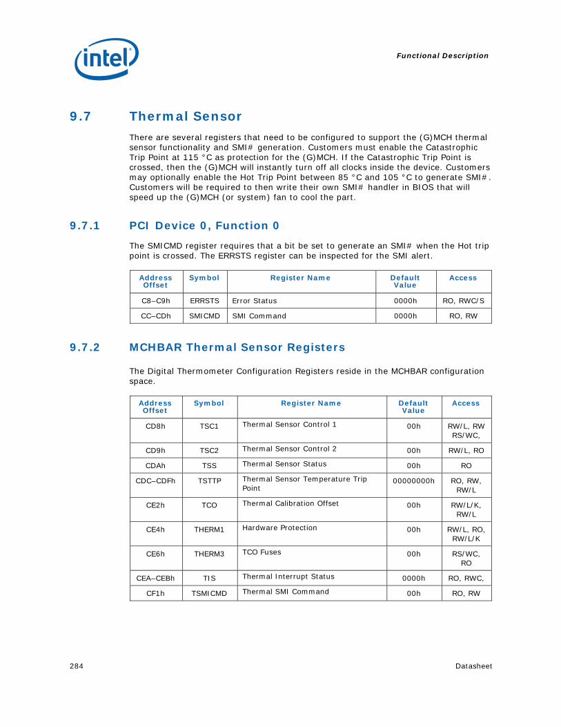
1.3.9 Thermal Sensor
(G)MCH Thermal Sensor support includes:
• Catastrophic Trip Point support for emergency clock gating for the (G)MCH at 115 °C
• Hot Trip Point support for SMI generation between 85 °C and 105 °C
§
Signal Description
Datasheet 27
2 Signal Description
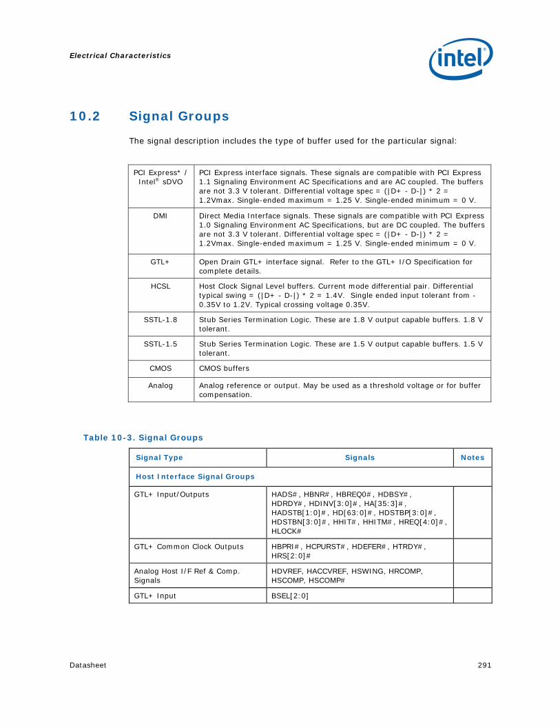
This chapter provides a detailed description of (G)MCH signals. The signals are arranged in functional groups according to their associated interface.
The following notations are used to describe the signal type:
Signal Type Description
PCI Express*
PCI Express interface signals. These signals are compatible with PCI Express 1.1 Signaling Environment AC Specifications and are AC coupled. The buffers are not 3.3 V tolerant. Differential voltage spec = (|D+ - D-|) * 2 = 1.2Vmax. Single-ended maximum = 1.25 V. Single-ended minimum = 0 V.
DMI Direct Media Interface signals. These signals are compatible with PCI Express 1.1 Signaling Environment AC Specifications, but are DC coupled. The buffers are not 3.3 V tolerant. Differential voltage spec = (|D+ - D-|) * 2 = 1.2Vmax. Single-ended maximum = 1.25 V. Single-ended minimum = 0 V.
CMOS CMOS buffers. 1.5 V tolerant.
COD CMOS Open Drain buffers. 3.3 V tolerant.
HVCMOS High Voltage CMOS buffers. 3.3 V tolerant.
HVIN High Voltage CMOS input-only buffers. 3.3 V tolerant.
SSTL_1.8 Stub Series Termination Logic. These are 1.8 V output capable buffers. 1.8 V tolerant.
A Analog reference or output. May be used as a threshold voltage or for buffer compensation.
GTL+ Gunning Transceiver Logic signaling technology. Implements a voltage level as defined by VTT of 1.2V.
Signal Description
28 Datasheet
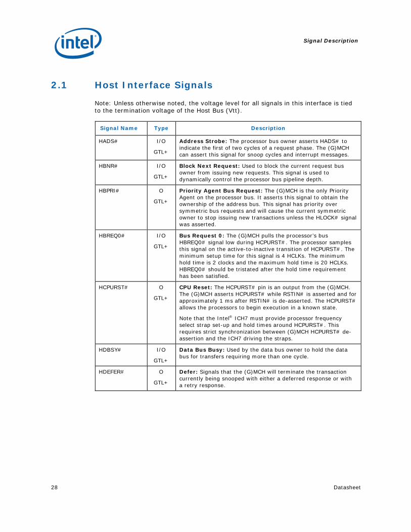
2.1 Host Interface Signals
Note: Unless otherwise noted, the voltage level for all signals in this interface is tied to the termination voltage of the Host Bus (Vtt).
Signal Name Type Description
HADS# I/O
GTL+
Address Strobe: The processor bus owner asserts HADS# to indicate the first of two cycles of a request phase. The (G)MCH can assert this signal for snoop cycles and interrupt messages.
HBNR# I/O
GTL+
Block Next Request: Used to block the current request bus owner from issuing new requests. This signal is used to dynamically control the processor bus pipeline depth.
HBPRI# O
GTL+
Priority Agent Bus Request: The (G)MCH is the only Priority Agent on the processor bus. It asserts this signal to obtain the ownership of the address bus. This signal has priority over symmetric bus requests and will cause the current symmetric owner to stop issuing new transactions unless the HLOCK# signal was asserted.
HBREQ0# I/O
GTL+
Bus Request 0: The (G)MCH pulls the processor’s bus HBREQ0# signal low during HCPURST#. The processor samples this signal on the active-to-inactive transition of HCPURST#. The minimum setup time for this signal is 4 HCLKs. The minimum hold time is 2 clocks and the maximum hold time is 20 HCLKs. HBREQ0# should be tristated after the hold time requirement has been satisfied.
HCPURST# O
GTL+
CPU Reset: The HCPURST# pin is an output from the (G)MCH. The (G)MCH asserts HCPURST# while RSTIN# is asserted and for approximately 1 ms after RSTIN# is de-asserted. The HCPURST# allows the processors to begin execution in a known state.
Note that the Intel® ICH7 must provide processor frequency select strap set-up and hold times around HCPURST#. This requires strict synchronization between (G)MCH HCPURST# de-assertion and the ICH7 driving the straps.
HDBSY# I/O
GTL+
Data Bus Busy: Used by the data bus owner to hold the data bus for transfers requiring more than one cycle.
HDEFER# O
GTL+
Defer: Signals that the (G)MCH will terminate the transaction currently being snooped with either a deferred response or with a retry response.
Signal Description
Datasheet 29
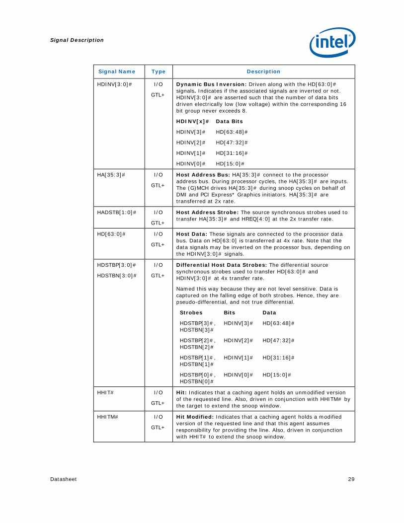
Signal Name Type Description
HDINV[3:0]# I/O
GTL+
Dynamic Bus Inversion: Driven along with the HD[63:0]# signals. Indicates if the associated signals are inverted or not. HDINV[3:0]# are asserted such that the number of data bits driven electrically low (low voltage) within the corresponding 16 bit group never exceeds 8.
HDINV[x]# Data Bits
HDINV[3]# HD[63:48]#
HDINV[2]# HD[47:32]#
HDINV[1]# HD[31:16]#
HDINV[0]# HD[15:0]#
HA[35:3]# I/O
GTL+
Host Address Bus: HA[35:3]# connect to the processor address bus. During processor cycles, the HA[35:3]# are inputs. The (G)MCH drives HA[35:3]# during snoop cycles on behalf of DMI and PCI Express* Graphics initiators. HA[35:3]# are transferred at 2x rate.
HADSTB[1:0]# I/O
GTL+
Host Address Strobe: The source synchronous strobes used to transfer HA[35:3]# and HREQ[4:0] at the 2x transfer rate.
HD[63:0]# I/O
GTL+
Host Data: These signals are connected to the processor data bus. Data on HD[63:0] is transferred at 4x rate. Note that the data signals may be inverted on the processor bus, depending on the HDINV[3:0]# signals.
HDSTBP[3:0]#
HDSTBN[3:0]#
I/O
GTL+
Differential Host Data Strobes: The differential source synchronous strobes used to transfer HD[63:0]# and HDINV[3:0]# at 4x transfer rate.
Named this way because they are not level sensitive. Data is captured on the falling edge of both strobes. Hence, they are pseudo-differential, and not true differential.
Strobes Bits Data
HDSTBP[3]#, HDSTBN[3]#
HDINV[3]# HD[63:48]#
HDSTBP[2]#, HDSTBN[2]#
HDINV[2]# HD[47:32]#
HDSTBP[1]#, HDSTBN[1]#
HDINV[1]# HD[31:16]#
HDSTBP[0]#, HDSTBN[0]#
HDINV[0]# HD[15:0]#
HHIT# I/O
GTL+
Hit: Indicates that a caching agent holds an unmodified version of the requested line. Also, driven in conjunction with HHITM# by the target to extend the snoop window.
HHITM# I/O
GTL+
Hit Modified: Indicates that a caching agent holds a modified version of the requested line and that this agent assumes responsibility for providing the line. Also, driven in conjunction with HHIT# to extend the snoop window.
Signal Description
30 Datasheet
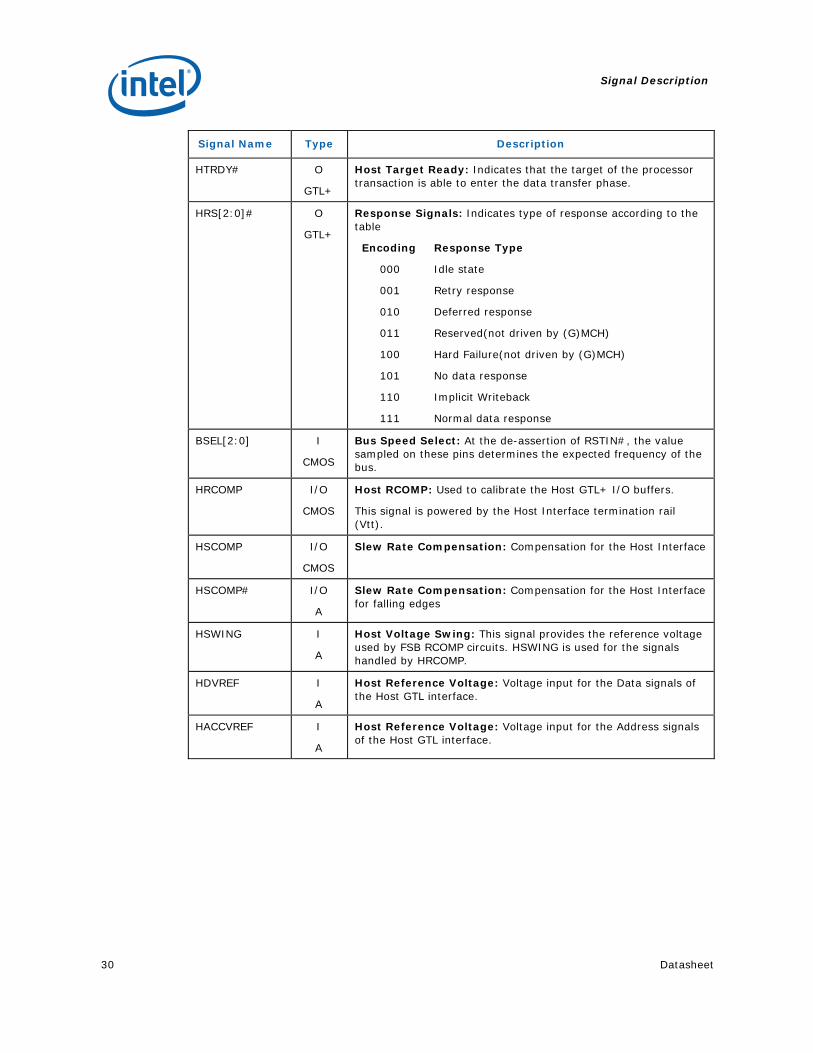
Signal Name Type Description
HTRDY# O
GTL+
Host Target Ready: Indicates that the target of the processor transaction is able to enter the data transfer phase.
HRS[2:0]# O
GTL+
Response Signals: Indicates type of response according to the table
Encoding Response Type
000 Idle state
001 Retry response
010 Deferred response
011 Reserved(not driven by (G)MCH)
100 Hard Failure(not driven by (G)MCH)
101 No data response
110 Implicit Writeback
111 Normal data response
BSEL[2:0] I
CMOS
Bus Speed Select: At the de-assertion of RSTIN#, the value sampled on these pins determines the expected frequency of the bus.
HRCOMP I/O
CMOS
Host RCOMP: Used to calibrate the Host GTL+ I/O buffers.
This signal is powered by the Host Interface termination rail (Vtt).
HSCOMP I/O
CMOS
Slew Rate Compensation: Compensation for the Host Interface
HSCOMP# I/O
A
Slew Rate Compensation: Compensation for the Host Interface for falling edges
HSWING I
A
Host Voltage Swing: This signal provides the reference voltage used by FSB RCOMP circuits. HSWING is used for the signals handled by HRCOMP.
HDVREF I
A
Host Reference Voltage: Voltage input for the Data signals of the Host GTL interface.
HACCVREF I
A
Host Reference Voltage: Voltage input for the Address signals of the Host GTL interface.
Signal Description
Datasheet 31
2.2 System Memory (DDR2) Interface Signals
2.2.1 System Memory Channel A Interface Signals
Signal Name Type Description
SCLK_A[2:0] O SSTL-1.8
SDRAM Differential Clock: (3 per DIMM), SCLK_A and its complement, SCLK_A# make a differential clock pair output. The crossing of the positive edge of SCLK_A and the negative edge of its complement SCLK_A# are used to sample the command and control signals on the SDRAM.
SCLK_A[2:0]# O SSTL-1.8
SDRAM Complementary Differential Clock: (3 per DIMM) These are the complementary differential DDR2 Clock signals.
SCS_A[1:0]# O SSTL-1.8
Chip Select: (1 per Rank) These signals select particular SDRAM components during the active state. There is one Chip Select for each SDRAM rank.
SMA_A[14:0] O SSTL-1.8
Memory Address: These signals are used to provide the multiplexed row and column address to the SDRAM.
SBS_A[2:0] O SSTL-1.8
Bank Select: These signals define which banks are selected within each SDRAM rank.
DDR2: 1-Gb technology uses 8 banks.
SRAS_A# O SSTL-1.8
Row Address Strobe: Used with SCAS_A# and SWE_A# (along with SCS_A#) to define the SDRAM commands.
SCAS_A# O SSTL-1.8
Column Address Strobe: Used with SRAS_A# and SWE_A# (along with SCS_A#) to define the SDRAM commands.
SWE_A# O SSTL-1.8
Write Enable: Used with SCAS_A# and SRAS_A# (along with SCS_A#) to define the SDRAM commands.
SDQ_A[63:0] I/O SSTL-1.8
Data Lines: SDQ_A signals interface to the SDRAM data bus.
SDM_A[7:0] O SSTL-1.8
Data Mask: When activated during writes, the corresponding data groups in the SDRAM are masked. There is one SDM_A bit for every data byte lane.
SDQS_A[7:0] I/O SSTL-1.8
Data Strobes: For DDR2, SDQS_A, and its complement SDQS_A# make up a differential strobe pair. The data is captured at the crossing point of SDQS_A and its complement SDQS_A# during read and write transactions.
SDQS_A[7:0]# I/O SSTL-1.8
Data Strobe Complements: These are the complementary DDR2 strobe signals.
SCKE_A[1:0] O SSTL-1.8
Clock Enable: (1 per Rank) SCKE_A is used to initialize the SDRAMs during power-up, to power-down SDRAM ranks, and to place all SDRAM ranks into and out of self-refresh during Suspend-to-RAM.
SODT_A[1:0] O SSTL-1.8
On Die Termination: Active On-die Termination Control signals for DDR2 devices.
Signal Description
32 Datasheet
2.2.2 System Memory Channel B Interface Signals
Signal Name Type Description
SCLK_B[2:0] O SSTL-1.8
SDRAM Differential Clock: (3 per DIMM) SCLK_B and its complement, SCLK_B#, make a differential clock pair output. The crossing of the positive edge of SCLK_B and the negative edge of its complement SCLK_B# are used to sample the command and control signals on the SDRAM.
SCLK_B[2:0]# O SSTL-1.8
SDRAM Complementary Differential Clock: (3 per DIMM) These are the complementary differential DDR2 Clock signals.
SCS_B[1:0]# O SSTL-1.8
Chip Select: (1 per Rank) These signals select particular SDRAM components during the active state. There is one Chip Select for each SDRAM rank
SMA_B[14:0] O SSTL-1.8
Memory Address: These signals are used to provide the multiplexed row and column address to the SDRAM.
SBS_B[2:0] O SSTL-1.8
Bank Select: These signals define which banks are selected within each SDRAM rank
DDR2: 1-Gb technology uses 8 banks.
SRAS_B# O SSTL-1.8
Row Address Strobe: Used with SCAS_B# and SWE_B# (along with SCS_B#) to define the SDRAM commands
SCAS_B# O SSTL-1.8
Column Address Strobe: Used with SRAS_B# and SWE_B# (along with SCS_B#) to define the SDRAM commands.
SWE_B# O SSTL-1.8
Write Enable: Used with SCAS_B# and SRAS_B# (along with SCS_B#) to define the SDRAM commands.
SDQ_B[63:0] I/O SSTL-1.8
Data Lines: SDQ_B signals interface to the SDRAM data bus.
SDM_B[7:0] O SSTL-1.8
Data Mask: When activated during writes, the corresponding data groups in the SDRAM are masked. There is one SBDM for every data byte lane.
SDQS_B[7:0] I/O SSTL-1.8
Data Strobes: For DDR2, SDQS_B, and its complement ,SDQS_B#, make up a differential strobe pair. The data is captured at the crossing point of SDQS_B and its complement SDQS_B# during read and write transactions.
SDQS_B[7:0]# I/O SSTL-1.8
Data Strobe Complements: These are the complementary DDR2 strobe signals.
SCKE_B[1:0] O SSTL-1.8
Clock Enable: (1 per Rank) SCKE_B is used to initialize the SDRAMs during power-up, to power-down SDRAM ranks, and to place all SDRAM ranks into and out of self-refresh during Suspend-to-RAM.
SODT_B[1:0] O SSTL-1.8
On Die Termination: Active On-die Termination Control signals for DDR2 devices.
Signal Description
Datasheet 33
2.2.3 DDR2 DRAM Reference and Compensation Signals
Signal Name Type Description
SRCOMP[3:0] I A
System Memory RCOMP
SVREF I A
SDRAM Reference Voltage: Reference voltage input for DQ, DQS, and DQS# input signals.
SMRCOMPVOL I A
System Memory RCOMP reference
SMRCOMPVOH I A
System Memory RCOMP reference
2.3 PCI Express* Interface Signals Signal Name Type Description
2.4 Analog Display Signals (Intel® 82G31 GMCH Only)
Signal Name Type Description
RED O
A
RED Analog Video Output: This signal is a CRT Analog video output from the internal color palette DAC. The DAC is designed for a 37.5 ohm routing impedance, but the terminating resistor to ground will be 75 ohms (e.g., 75 ohm resistor on the board, in parallel with a 75 ohm CRT load).
RED# O
A
RED# Analog Output: This signal is an analog video output from the internal color palette DAC. It should be shorted to the ground plane.
GREEN O
A
GREEN Analog Video Output: This signal is a CRT Analog video output from the internal color palette DAC. The DAC is designed for a 37.5 ohm routing impedance, but the terminating resistor to ground will be 75 ohms (e.g., 75 ohm resistor on the board, in parallel with a 75 ohm CRT load).
GREEN# O
A
GREEN# Analog Output: This signal is an analog video output from the internal color palette DAC. It should be shorted to the ground plane.
BLUE O
A
BLUE Analog Video Output: This signal is a CRT Analog video output from the internal color palette DAC. The DAC is designed for a 37.5 ohm routing impedance, but the terminating resistor to ground will be 75 ohms (e.g., 75 ohm resistor on the board, in parallel with a 75 ohm CRT load).
BLUE# O
A
BLUE# Analog Output: This signal is an analog video output from the internal color palette DAC. It should be shorted to the ground plane.
REFSET O
A
Resistor Set: Set point resistor for the internal color palette DAC. A 255 ohm 1% resistor is required between REFSET and motherboard ground.
HSYNC O 3.3V CMOS
CRT Horizontal Synchronization: This signal is used as the horizontal sync (polarity is programmable) or “sync interval”, 3.3 V output
VSYNC O 3.3V CMOS
CRT Vertical Synchronization: This signal is used as the vertical sync (polarity is programmable) 3.3V output.
DDC_CLK I/O 3.3V CMOS
Monitor Control Clock
DDC_DATA I/O 3.3V CMOS
Monitor Control Data
Signal Description
Datasheet 35
2.5 Clocks, Reset, and Miscellaneous
Signal Name Type Description
HCLKP
HCLKN
I
HCSL
Differential Host Clock In: These pins receive a differential host clock from the external clock synthesizer. This clock is used by all of the (G)MCH logic that is in the Host clock domain. Memory domain clocks are also derived from this source.
GCLKP
GCLKN
I
HCSL
Differential PCI Express* Graphics Clock In: These pins receive a differential 100 MHz Serial Reference clock from the external clock synthesizer. This clock is used to generate the clocks necessary for the support of PCI Express.
DREFCLKN
DREFCLKP
I
HCSL
Display PLL Differential Clock In
RSTIN# I
HVIN
Reset In: When asserted, this signal will asynchronously reset the (G)MCH logic. This signal is connected to the PCIRST# output of the Intel® ICH7. All PCI Express Graphics Attach output signals will also tri-state compliant to PCI Express* Specification Rev 1.1.
This input should have a Schmitt trigger to avoid spurious resets.
This signal is required to be 3.3V tolerant.
EXP_SLR I
CMOS
PCI Express* Static Lane Reversal/Form Factor Selection: (G)MCH’s PCI Express lane numbers are reversed to differentiate BTX and ATX form factors 0 = (G)MCH PCI Express lane numbers are reversed (BTX)
1 = Normal operation (ATX)
BSEL2
BSEL1
BSEL0
I
HCSL
Bus Speed Select: At the assertion of PWROK, the value sampled on these pins determines the expected frequency of the bus. Theses pins must also be routed to probe points or to the XDP connector when applicable
EXP_EN I
GTL+
Concurrent PCI Express Port Enable: Concurrent SDVO and PCI Express 0 = Only SDVO or PCI Express is operational.
1 = Both SDVO and PCI Express are operating simultaneously via the PCI Express port.
NOTE: For the 82P31 MCH, this signal should be connected to ground.
PWROK I/O
SSTL
Power OK: When asserted, PWROK is an indication to the (G)MCH that core power has been stable for at least 10 us.
ICH_SYNC# O
HVCMOS
Maintains synchronization between (G)MCH and ICH
Signal Description
36 Datasheet
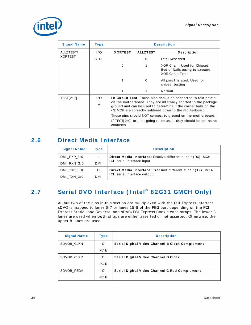
Signal Name Type Description
ALLZTEST/ XORTEST
I/O
GTL+
XORTEST ALLZTEST Description
0 0 Intel Reserved
0 1 XOR Chain. Used for Chipset Bed of Nails tesing to execute XOR Chain Test
1 0 All pins tristated. Used for chipset testing
1 1 Normal
TEST[2:0] I/O
A
In Circuit Test: These pins should be connected to test points on the motherboard. They are internally shorted to the package ground and can be used to determine if the corner balls on the (G)MCH are correctly soldered down to the motherboard.
These pins should NOT connect to ground on the motherboard.
If TEST[2:0] are not going to be used, they should be left as no connects.
2.6 Direct Media Interface Signal Name Type Description
DMI_RXP_3:0
DMI_RXN_3:0
I
DMI
Direct Media Interface: Receive differential pair (RX). MCH-ICH serial interface input.
DMI_TXP_3:0
DMI_TXN_3:0
O
DMI
Direct Media Interface: Transmit differential pair (TX). MCH-ICH serial interface output.
2.7 Serial DVO Interface (Intel® 82G31 GMCH Only)
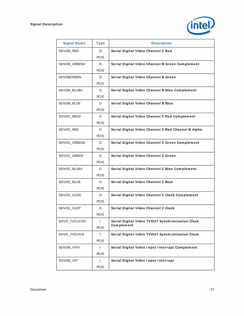
All but two of the pins in this section are multiplexed with the PCI Express interface. sDVO is mapped to lanes 0-7 or lanes 15-8 of the PEG port depending on the PCI Express Static Lane Reversal and sDVO/PCI Express Coexistence straps. The lower 8 lanes are used when both straps are either asserted or not asserted. Otherwise, the upper 8 lanes are used.
Signal Name Type Description
SDVOB_CLKN O
PCIE
Serial Digital Video Channel B Clock Complement
SDVOB_CLKP O
PCIE
Serial Digital Video Channel B Clock
SDVOB_RED# O
PCIE
Serial Digital Video Channel C Red Complement
Signal Description
Datasheet 37
Signal Name Type Description
SDVOB_RED O
PCIE
Serial Digital Video Channel C Red
SDVOB_GREEN# O
PCIE
Serial Digital Video Channel B Green Complement
SDVOBGREEN O
PCIE
Serial Digital Video Channel B Green
SDVOB_BLUE# O
PCIE
Serial Digital Video Channel B Blue Complement
SDVOB_BLUE O
PCIE
Serial Digital Video Channel B Blue
SDVOC_RED# O
PCIE
Serial Digital Video Channel C Red Complement
SDVOC_RED O
PCIE
Serial Digital Video Channel C Red Channel B Alpha
SDVOC_GREEN# O
PCIE
Serial Digital Video Channel C Green Complement
SDVOC_GREEN O
PCIE
Serial Digital Video Channel C Green
SDVOC_BLUE# O
PCIE
Serial Digital Video Channel C Blue Complement
SDVOC_BLUE O
PCIE
Serial Digital Video Channel C Blue
SDVOC_CLKN O
PCIE
Serial Digital Video Channel C Clock Complement
SDVOC_CLKP O
PCIE
Serial Digital Video Channel C Clock
SDVO_TVCLKIN# I
PCIE
Serial Digital Video TVOUT Synchronization Clock Complement
The (G)MCH supports 64 GB (36 bit) of host address space and 64 KB+3 of addressable I/O space. There is a programmable memory address space under the 1 MB region which is divided into regions which can be individually controlled with programmable attributes such as Disable, Read/Write, Write Only, or Read Only. Attribute programming is described in the Register Description section. This section focuses on how the memory space is partitioned and what the separate memory regions are used for. I/O address space has simpler mapping and is explained near the end of this section.
Note: Address mapping information for the Integrated Graphics Device applies to the 82G31 GMCH only. The 82P31 MCH does not have an IGD.
The (G)MCH supports PEG port upper pre-fetchable base/limit registers. This allows the PEG unit to claim IO accesses above 36 bit, complying with the PCI Express Specification. Addressing of greater than 4 GB is allowed on either the DMI Interface or PCI Express interface. The (G)MCH supports a maximum of 4 GB of DRAM. No DRAM memory will be accessible above 4 GB.
When running in internal graphics mode, writes to GMADR range linear range are supported. Write accesses to linear regions are supported from DMI only. Write accesses to tileX and tileY regions (defined via fence registers) are not supported from DMI or the PEG port. GMADR read accesses are not supported from either DMI or PEG.
In the following sections, it is assumed that all of the compatibility memory ranges reside on the DMI Interface. The exception to this rule is VGA ranges, which may be mapped to PCI-Express, DMI, or to the internal graphics device (IGD). In the absence of more specific references, cycle descriptions referencing PCI should be interpreted as the DMI Interface/PCI, while cycle descriptions referencing PCI Express or IGD are related to the PCI Express bus or the internal graphics device respectively. The (G)MCH does not remap APIC or any other memory spaces above TOLUD (Top of Low Usable DRAM). The TOLUD register is set to the appropriate value by BIOS. The reclaim base/reclaim limit registers remap logical accesses bound for addresses above 4 GB onto physical addresses that fall within DRAM.
System Address Map
42 Datasheet
The Address Map includes a number of programmable ranges:
• 1. Device 0 ⎯ PXPEPBAR – Express port registers. Necessary for setting up VC1 as an
isochronous channel using time based weighted round robin arbitration. (4 KB window)
⎯ MCHBAR – Memory mapped range for internal (G)MCH registers. For example, memory buffer register controls. (16 KB window)
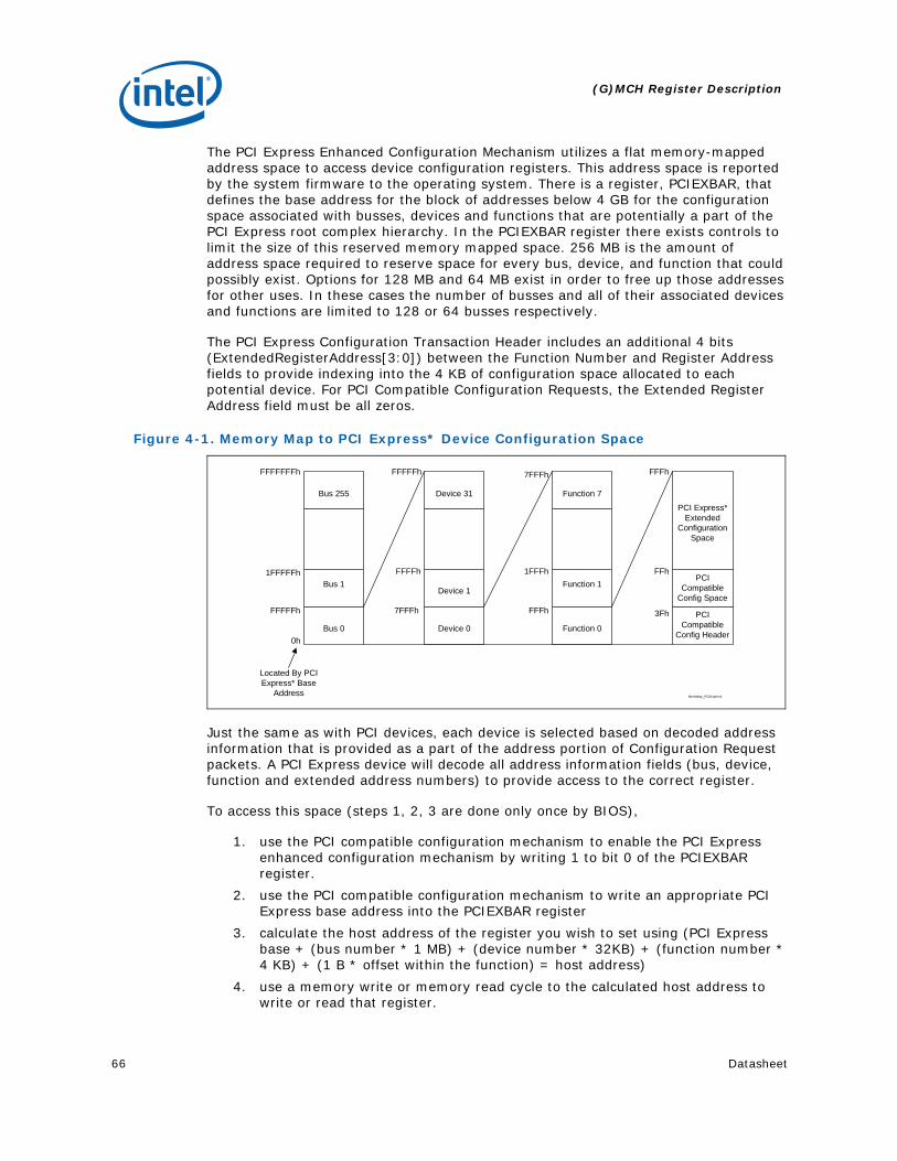
⎯ PCIEXBAR – Flat memory-mapped address spaced to access device configuration registers. This mechanism can be used to access PCI configuration space (0–FFh) and Extended configuration space (100h–FFFh) for PCI Express devices. This enhanced configuration access mechanism is defined in the PCI Express specification. (64 MB, 128 MB, or 256 MB window).
⎯ DMIBAR –This window is used to access registers associated with the Direct Media Interface (DMI) register memory range. (4 KB window)
⎯ GGCGMS (82G31 GMCH only) – GMCH graphics control register, Graphics Mode Select. Used to select the amount of main memory that is pre-allocated to support the internal graphics device in VGA (non-linear) and Native (linear) modes. (0-256 MB options).
⎯ GGCGGMS (82G31 GMCH only) – GMCH graphics control register, GTT Graphics Memory Size. GGCGGMS is used to select the amount of main memory that is pre-allocated to support the Internal Graphics Translation Table. (0-2 MB options).
window ⎯ IOBASE1/IOLIMIT1 – PCI Express port IO access window.
• Device 2, Function 0 (82G31 GMCH only) ⎯ MMADR – IGD registers and internal graphics instruction port. (512 KB
window) ⎯ IOBAR – IO access window for internal graphics. Though this window
address/data register pair, using I/O semantics, the IGD and internal graphics instruction port registers can be accessed. Note, this allows accessing the same registers as MMADR. In addition, the IOBAR can be used to issue writes to the GTTADR table.
⎯ GTTADR – Internal graphics translation table location. (1 MB window). Note that the Base of GTT stolen Memory register (Device 0 A8) indicates the physical address base which is 1 MB aligned.
• Device 2, Function 1 (82G31 GMCH only) ⎯ MMADR – Function 1 IGD registers and internal graphics instruction port. (512
KB window)
System Address Map
Datasheet 43
The rules for the above programmable ranges are:
1. ALL of these ranges MUST be unique and NON-OVERLAPPING. It is the BIOS or system designers' responsibility to limit memory population so that adequate PCI, PCI Express, High BIOS, PCI Express Memory Mapped space, and APIC memory space can be allocated.
2. There are NO Hardware Interlocks to prevent problems in the case of overlapping ranges.
3. Accesses to overlapped ranges may produce indeterminate results.
4. The only peer-to-peer cycles allowed below the top of Low Usable memory (register TOLUD) are DMI Interface to PCI Express VGA range writes. Note that peer to peer cycles to the Internal Graphics VGA range are not supported.
Figure 3-1 represents the system memory address map in a simplified form.
Figure 3-1. System Address Ranges
PCI Memory Address Range
(subtractively decoded to
DMI
Device 1
Bars
Device 0
Bars
Independently Programmable Non-Overlapping Windows
Main Memory Reclaim Address Range
Reclaim Limit = Reclaim Base +X(64 MB Aligned)TOUUD Base
Reclaim Base(64 MB Aligned)
Main Memory Address Range
Device 3
Device 2
Device 1
Bars
Device 0 GGC (GFX
Stolen Mem)
Device 0
Bars
TOLUD Base
(64 MB Aligned)
PCI Memory Address Range
(subtractively decoded to
DMI)
Independently Programmable Non-Overlapping Windows
TSEG
Main Memory Address Range
Legacy Address Range0
1 MB
64 GB
TOM 64 MB AlignedEP-UMA
(1 – 64 MB)0 – 63 MB Unusable
EP Stolen Base
64 MB Aligned
1 MB Aligned
OS Visible > 4 GB
4 GB
X OS Invisible Reclaim
GFX Stolen (1 – 64 MB)
TSEG (0 – 8 MB)
OS Visible < 4 GB
64 MB Aligned for Reclaim
1 MB Aligned
1 MB Aligned
Memap_Sys_Addr_Ranges
Host/System View
Physical Memory(DRAM Controller
View)
Device 3
M HBA
System Address Map
44 Datasheet
3.1 Legacy Address Range
This area is divided into the following address regions:
• 0 – 640 KB – DOS Area
• 640 – 768 KB – Legacy Video Buffer Area
• 768 – 896 KB in 16 KB sections (total of 8 sections) – Expansion Area
• 896 – 960 KB in 16 KB sections (total of 4 sections) – Extended System BIOS Area
• 960 KB – 1 MB Memory – System BIOS Area
Figure 3-2. DOS Legacy Address Range
Expansion Area128KB (16KBx8)
000C_0000h
000D_FFFFh896KB
Extended System BIOS (Lower)64KB (16KBx4)000E_0000h
000E_FFFFh960KB
Legacy Video Area(SMM Memory)
128KB000A_0000h
000B_FFFFh768KB
DOS Area
0000_0000h
0009_FFFFh640KB
System BIOS (Upper)64KB000F_0000h
000F_FFFFh1MB
System Address Map
Datasheet 45
3.1.1 DOS Range (0h – 9_FFFFh)
The DOS area is 640 KB (0000_0000h – 0009_FFFFh) in size and is always mapped to the main memory controlled by the (G)MCH.
3.1.2 Legacy Video Area (A_0000h-B_FFFFh)
The legacy 128KB VGA memory range, frame buffer, (000A_0000h – 000B_FFFFh) can be mapped to IGD (Device 2), to PCI Express (Device 1), and/or to the DMI Interface. The appropriate mapping depends on which devices are enabled and the programming of the VGA steering bits. Based on the VGA steering bits, priority for VGA mapping is constant. The (G)MCH always decodes internally mapped devices first. Internal to the (G)MCH, decode precedence is always given to IGD. The (G)MCH always positively decodes internally mapped devices, namely the IGD (82G31 GMCH only) and PCI-Express. Subsequent decoding of regions mapped to PCI Express or the DMI Interface depends on the Legacy VGA configuration bits (VGA Enable & MDAP). This region is also the default for SMM space.
Compatible SMRAM Address Range (A_0000h-B_FFFFh)
When compatible SMM space is enabled, SMM-mode processor accesses to this range are routed to physical system DRAM at 000A 0000h – 000B FFFFh. Non-SMM-mode processor accesses to this range are considered to be to the Video Buffer Area as described above. PCI Express and DMI originated cycles to enabled SMM space are not allowed and are considered to be to the Video Buffer Area, if IGD on the 82G31 GMCH is not enabled as the VGA device. PCI Express and DMI initiated cycles are attempted as Peer cycles, and will master abort on PCI if no external VGA device claims them.
Monochrome Adapter (MDA) Range (B_0000h-B_7FFFh)
Legacy support requires the ability to have a second graphics controller (monochrome) in the system. Accesses in the standard VGA range are forwarded to IGD, PCI Express, or the DMI Interface (depending on configuration bits). Since the monochrome adapter may be mapped to anyone of these devices, the (G)MCH must decode cycles in the MDA range (000B_0000h - 000B_7FFFh) and forward either to IGD, PCI Express, or the DMI Interface. This capability is controlled by a VGA steering bits and the legacy configuration bit (MDAP bit). In addition to the memory range B0000h to B7FFFh, the (G)MCH decodes IO cycles at 3B4h, 3B5h, 3B8h, 3B9h, 3BAh and 3BFh and forwards them to the either IGD, PCI-Express, and/or the DMI Interface.
PEG 16-bit VGA Decode
The PCI to PCI Bridge Architecture Specification Revision 1.2, it is required that 16-bit VGA decode be a feature.
System Address Map
46 Datasheet
3.1.3 Expansion Area (C_0000h-D_FFFFh)
This 128 KB ISA Expansion region (000C_0000h – 000D_FFFFh) is divided into eight 16 KB segments. Each segment can be assigned one of four Read/Write states: read-only, write-only, read/write, or disabled. Typically, these blocks are mapped through (G)MCH and are subtractive decoded to ISA space. Memory that is disabled is not remapped.
Non-snooped accesses from PCI Express or DMI to this region are always sent to DRAM.
Table 3-1. Expansion Area Memory Segments
Memory Segments Attributes Comments
0C0000h – 0C3FFFh WE RE Add-on BIOS
0C4000h – 0C7FFFh WE RE Add-on BIOS
0C8000h – 0CBFFFh WE RE Add-on BIOS
0CC000h – 0CFFFFh WE RE Add-on BIOS
0D0000h – 0D3FFFh WE RE Add-on BIOS
0D4000h – 0D7FFFh WE RE Add-on BIOS
0D8000h – 0DBFFFh WE RE Add-on BIOS
0DC000h – 0DFFFFh WE RE Add-on BIOS
System Address Map
Datasheet 47
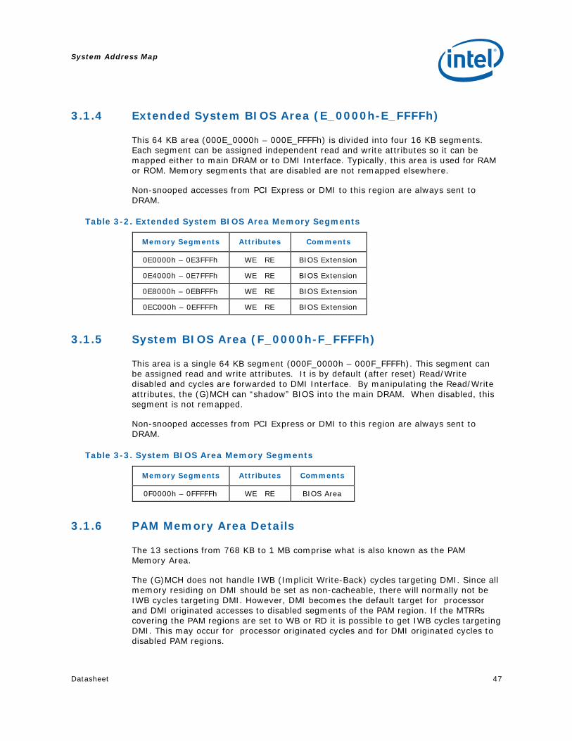
3.1.4 Extended System BIOS Area (E_0000h-E_FFFFh)
This 64 KB area (000E_0000h – 000E_FFFFh) is divided into four 16 KB segments. Each segment can be assigned independent read and write attributes so it can be mapped either to main DRAM or to DMI Interface. Typically, this area is used for RAM or ROM. Memory segments that are disabled are not remapped elsewhere.
Non-snooped accesses from PCI Express or DMI to this region are always sent to DRAM.
Table 3-2. Extended System BIOS Area Memory Segments
Memory Segments Attributes Comments
0E0000h – 0E3FFFh WE RE BIOS Extension
0E4000h – 0E7FFFh WE RE BIOS Extension
0E8000h – 0EBFFFh WE RE BIOS Extension
0EC000h – 0EFFFFh WE RE BIOS Extension
3.1.5 System BIOS Area (F_0000h-F_FFFFh)
This area is a single 64 KB segment (000F_0000h – 000F_FFFFh). This segment can be assigned read and write attributes. It is by default (after reset) Read/Write disabled and cycles are forwarded to DMI Interface. By manipulating the Read/Write attributes, the (G)MCH can “shadow” BIOS into the main DRAM. When disabled, this segment is not remapped.
Non-snooped accesses from PCI Express or DMI to this region are always sent to DRAM.
Table 3-3. System BIOS Area Memory Segments
Memory Segments Attributes Comments
0F0000h – 0FFFFFh WE RE BIOS Area
3.1.6 PAM Memory Area Details
The 13 sections from 768 KB to 1 MB comprise what is also known as the PAM Memory Area.
The (G)MCH does not handle IWB (Implicit Write-Back) cycles targeting DMI. Since all memory residing on DMI should be set as non-cacheable, there will normally not be IWB cycles targeting DMI. However, DMI becomes the default target for processor and DMI originated accesses to disabled segments of the PAM region. If the MTRRs covering the PAM regions are set to WB or RD it is possible to get IWB cycles targeting DMI. This may occur for processor originated cycles and for DMI originated cycles to disabled PAM regions.
System Address Map
48 Datasheet
For example, say that a particular PAM region is set for “Read Disabled” and the MTRR associated with this region is set to WB. A DMI master generates a memory read targeting the PAM region. A snoop is generated on the FSB and the result is an IWB. Since the PAM region is “Read Disabled” the default target for the Memory Read becomes DMI. The IWB associated with this cycle will cause the (G)MCH to hang.
Non-snooped accesses from PCI Express or DMI to this region are always sent to DRAM.
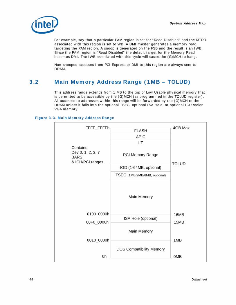
3.2 Main Memory Address Range (1MB – TOLUD)
This address range extends from 1 MB to the top of Low Usable physical memory that is permitted to be accessible by the (G)MCH (as programmed in the TOLUD register). All accesses to addresses within this range will be forwarded by the (G)MCH to the DRAM unless it falls into the optional TSEG, optional ISA Hole, or optional IGD stolen VGA memory.
Figure 3-3. Main Memory Address Range
Main Memory
ISA Hole (optional)
DOS Compatibility Memory
0h
FLASHFFFF_FFFFh
00F0_0000h 15MB
16MB0100_0000h
0MB
TOLUD
APIC
Main Memory
0010_0000h 1MB
IGD (1-64MB, optional)
TSEG (1MB/2MB/8MB, optional)
LT
PCI Memory Range
4GB Max
Contains:Dev 0, 1, 2, 3, 7 BARS& ICH/PCI ranges
System Address Map
Datasheet 49
3.2.1 ISA Hole (15 MB-16 MB)
A hole can be created at 15 MB–16 MB as controlled by the fixed hole enable in Device 0 space. Accesses within this hole are forwarded to the DMI Interface. The range of physical DRAM memory disabled by opening the hole is not remapped to the top of the memory – that physical DRAM space is not accessible. This 15 MB–16 MB hole is an optionally enabled ISA hole.
Video accelerators originally used this hole. It is also used by validation and customer SV teams for some of their test cards. That is why it is being supported. There is no inherent BIOS request for the 15 MB—16 MB window.
3.2.2 TSEG TSEG is optionally 1 MB, 2 MB, or 8 MB in size. TSEG is below IGD stolen memory, which is at the top of Low Usable physical memory (TOLUD). SMM-mode processor accesses to enabled TSEG access the physical DRAM at the same address. Non- processor originated accesses are not allowed to SMM space. PCI Express, DMI, and Internal Graphics originated cycle to enabled SMM space are handled as invalid cycle type with reads and writes to location 0 and byte enables turned off for writes. When the extended SMRAM space is enabled, processor accesses to the TSEG range without SMM attribute or without WB attribute are also forwarded to memory as invalid accesses. Non-SMM-mode Write Back cycles that target TSEG space are completed to DRAM for cache coherency. When SMM is enabled, the maximum amount of memory available to the system is equal to the amount of physical DRAM minus the value in the TSEG register which is fixed at 1 MB, 2 MB or 8 MB.
3.2.3 Pre-allocated Memory Voids of physical addresses that are not accessible as general system memory and reside within system memory address range (< TOLUD) are created for SMM-mode, legacy VGA graphics compatibility, and graphics GTT stolen memory. It is the responsibility of BIOS to properly initialize these regions. Table 3-4 details the location and attributes of the regions. Enabling/Disabling these ranges are described in the (G)MCH Control Register Device 0 (GCC).
Table 3-4. Pre-allocated Memory Example for 64 MB DRAM, 1 MB VGA, 1 MB GTT stolen and 1 MB TSEG
Memory Segments Attributes Comments
0000_0000h – 03CF_FFFFh R/W Available System Memory 61 MB
03D0_0000h – 03DF_FFFFh SMM Mode Only - Processor Reads
NOTES: 1. References to IDG and graphics STOLEN memory is only for the 82G31 GMCH.
System Address Map
50 Datasheet
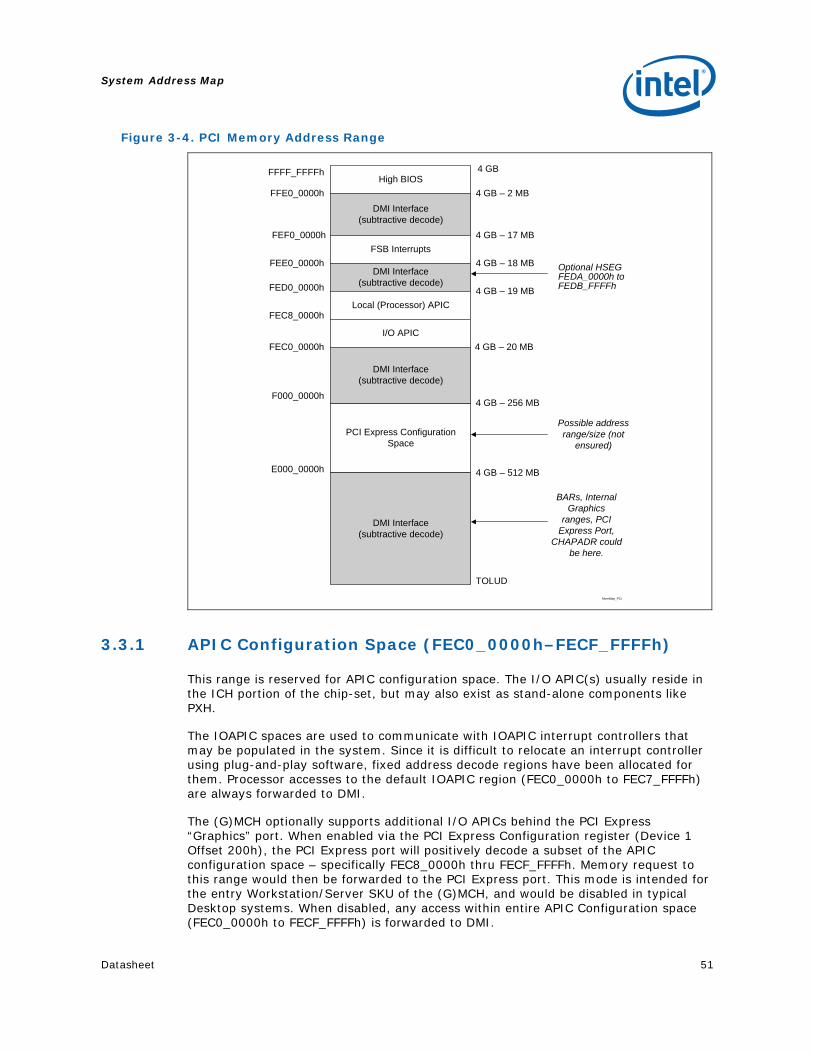
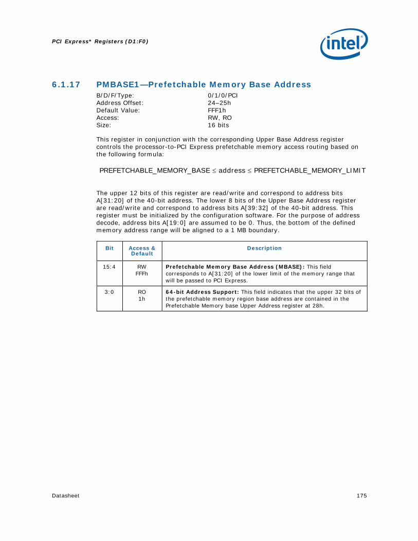
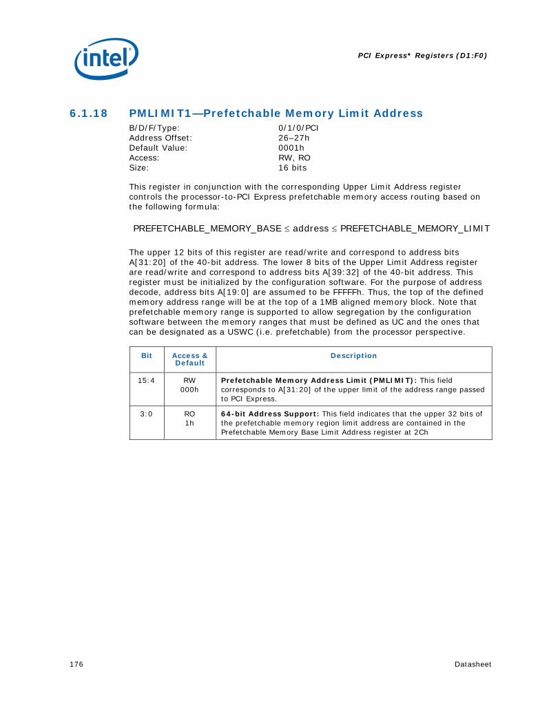
3.3 PCI Memory Address Range (TOLUD – 4 GB)
This address range, from the top of low usable DRAM (TOLUD) to 4 GB is normally mapped to the DMI Interface.
Device 0 exceptions are:
• Addresses decoded to the Express port registers (PXPEPBAR)
• Addresses decoded to the memory mapped range for internal (G)MCH registers (MCHBAR)
• Addresses decoded to the flat memory-mapped address spaced to access device configuration registers (PCIEXBAR)
• Addresses decoded to the registers associated with the Direct Media Interface (DMI) register memory range. (DMIBAR)
With PCI Express port, there are two exceptions to this rule:
• Addresses decoded to the PCI Express Memory Window defined by the MBASE1, MLIMIT1, registers are mapped to PCI Express.
• Addresses decoded to the PCI Express prefetchable Memory Window defined by the PMBASE1, PMLIMIT1, registers are mapped to PCI Express.
In integrated graphics configurations, there are exceptions to this rule:
• Addresses decoded to the IGD registers and internal graphics instruction port (Function 0 MMADR, Function 1 MMADR)
• Addresses decode to the internal graphics translation window (GMADR)
• Addresses decode to the Internal graphics translation table (GTTADR)
Some of the MMIO Bars may be mapped to this range or to the range above TOUUD.
There are sub-ranges within the PCI Memory address range defined as APIC Configuration Space, FSB Interrupt Space, and High BIOS Address Range. The exceptions listed above for internal graphics and the PCI Express ports MUST NOT overlap with these ranges.
System Address Map
Datasheet 51
Figure 3-4. PCI Memory Address Range
DMI Interface(subtractive decode)
FEF0_0000h
4 GB – 2 MB
FSB InterruptsFEE0_0000h
PCI Express Configuration Space
E000_0000h
High BIOSFFE0_0000h
FFFF_FFFFh 4 GB
4 GB – 17 MB
DMI Interface(subtractive decode)FED0_0000h
4 GB – 18 MB
Local (Processor) APICFEC8_0000h
4 GB – 19 MB
I/O APICFEC0_0000h 4 GB – 20 MB
DMI Interface(subtractive decode)
F000_0000h4 GB – 256 MB
Possible address range/size (not
ensured)
4 GB – 512 MB
DMI Interface(subtractive decode)
TOLUD
Optional HSEG FEDA_0000h to FEDB_FFFFh
BARs, Internal Graphics
ranges, PCI Express Port,
CHAPADR could be here.
MemMap_PCI
3.3.1 APIC Configuration Space (FEC0_0000h–FECF_FFFFh)
This range is reserved for APIC configuration space. The I/O APIC(s) usually reside in the ICH portion of the chip-set, but may also exist as stand-alone components like PXH.
The IOAPIC spaces are used to communicate with IOAPIC interrupt controllers that may be populated in the system. Since it is difficult to relocate an interrupt controller using plug-and-play software, fixed address decode regions have been allocated for them. Processor accesses to the default IOAPIC region (FEC0_0000h to FEC7_FFFFh) are always forwarded to DMI.
The (G)MCH optionally supports additional I/O APICs behind the PCI Express “Graphics” port. When enabled via the PCI Express Configuration register (Device 1 Offset 200h), the PCI Express port will positively decode a subset of the APIC configuration space – specifically FEC8_0000h thru FECF_FFFFh. Memory request to this range would then be forwarded to the PCI Express port. This mode is intended for the entry Workstation/Server SKU of the (G)MCH, and would be disabled in typical Desktop systems. When disabled, any access within entire APIC Configuration space (FEC0_0000h to FECF_FFFFh) is forwarded to DMI.
System Address Map
52 Datasheet
3.3.2 HSEG (FEDA_0000h–FEDB_FFFFh)
This optional segment from FEDA_0000h to FEDB_FFFFh provides a remapping window to SMM Memory. It is sometimes called the High SMM memory space. SMM-mode processor accesses to the optionally enabled HSEG are remapped to 000A-_0000h – 000B_FFFFh. Non-SMM-mode processor accesses to enabled HSEG are considered invalid and are terminated immediately on the FSB. The exceptions to this rule are Non-SMM-mode Write Back cycles which are remapped to SMM space to maintain cache coherency. PCI Express and DMI originated cycles to enabled SMM space are not allowed. Physical DRAM behind the HSEG transaction address is not remapped and is not accessible. All cacheline writes with WB attribute or Implicit write backs to the HSEG range are completed to DRAM like an SMM cycle.
3.3.3 FSB Interrupt Memory Space (FEE0_0000–FEEF_FFFF)
The FSB Interrupt space is the address used to deliver interrupts to the FSB. Any device on PCI Express or DMI may issue a Memory Write to 0FEEx_xxxxh. The (G)MCH will forward this Memory Write along with the data to the FSB as an Interrupt Message Transaction. The (G)MCH terminates the FSB transaction by providing the response and asserting HTRDYB. This Memory Write cycle does not go to DRAM.
3.3.4 High BIOS Area
The top 2 MB (FFE0_0000h – FFFF_FFFFh) of the PCI Memory Address Range is reserved for System BIOS (High BIOS), extended BIOS for PCI devices, and the A20 alias of the system BIOS. The processor begins execution from the High BIOS after reset. This region is mapped to DMI Interface so that the upper subset of this region aliases to 16 MB–256 KB range. The actual address space required for the BIOS is less than 2 MB but the minimum processor MTRR range for this region is 2 MB so that full 2 MB must be considered.
3.4 Main Memory Address Space (4 GB to TOUUD)
The (G)MCH supports 36 bit addressing. The maximum main memory size supported is 4 GB total DRAM memory. A hole between TOLUD and 4 GB occurs when main memory size approaches 4 GB or larger. As a result, TOM, and TOUUD registers and RECLAIMBASE/RECLAIMLIMIT registers become relevant.
The new reclaim configuration registers exist to reclaim lost main memory space. The greater than 32 bit reclaim handling will be handled similar to other (G)MCHs Upstream read and write accesses above 36-bit addressing will be treated as invalid cycles by PEG and DMI.
Top of Memory
The “Top of Memory” (TOM) register reflects the total amount of populated physical memory. This is NOT necessarily the highest main memory address (holes may exist in main memory address map due to addresses allocated for memory mapped I/O above TOM).
System Address Map
Datasheet 53
The Top of Upper Usable Dram (TOUUD) register reflects the total amount of addressable DRAM. If reclaim is enabled, then it will reflect the reclaim limit. TOLUD register is restricted to 4 GB memory (A[31:20]). When reclaim is enabled, TOLUD must be 64 MB aligned, but when reclaim is disabled, TOLUD can be 1 MB aligned.
C1DRB3 cannot be used directly to determine the effective size of memory as the values programmed in the DRBs depend on the memory mode (stacked, interleaved). The Reclaim Base/Limit registers also can not be used because reclaim can be disabled. The C0DRB3 register is used for memory channel identification (channel 0 vs. channel 1) in the case of stacked memory.
3.4.1 Memory Re-claim Background
The following are examples of Memory Mapped IO devices are typically located below 4 GB:
• High BIOS • HSEG • TSEG • Graphics stolen • GTT stolen • XAPIC • Local APIC • FSB Interrupts • Mbase/Mlimit • Memory Mapped IO space that supports only 32 B addressing
The (G)MCH provides the capability to re-claim the physical memory overlapped by the Memory Mapped IO logical address space. The (G)MCH re-maps physical memory from the Top of Low Memory (TOLUD) boundary up to the 4 GB boundary to an equivalent sized logical address range.
3.4.2 Memory Reclaiming
An incoming address (referred to as a logical address) is checked to see if it falls in the memory re-map window. The bottom of the re-map window is defined by the value in the RECLAIMBASE register. The top of the re-map window is defined by the value in the RECLAIMLIMIT register. An address that falls within this window is reclaimed to the physical memory starting at the address defined by the TOLUD register. The TOLUD register must be 64 MB aligned when RECLAIM is enabled, but can be 1 MB aligned when reclaim is disabled.
3.5 PCI Express* Configuration Address Space
There is a device 0 register, PCIEXBAR, which defines the base address for the configuration space associated with all devices and functions that are potentially a part of the PCI Express root complex hierarchy. The size of this range is programmable because the Intel G31/P31 Express chipset BIOS must assign this address range such that it will not conflict with any other address ranges.
See the configuration portion of this document for more details.
System Address Map
54 Datasheet
3.6 PCI Express* Graphics Attach (PEG)
The (G)MCH can be programmed to direct memory accesses to the PCI Express interface when addresses are within either of two ranges specified via registers in (G)MCH’s Device 1 configuration space.
• The first range is controlled via the Memory Base Register (MBASE) and Memory Limit Register (MLIMIT) registers.
• The second range is controlled via the Pre-fetchable Memory Base (PMBASE) and Pre-fetchable Memory Limit (PMLIMIT) registers.
Conceptually, address decoding for each range follows the same basic concept. The top 12 bits of the respective Memory Base and Memory Limit registers correspond to address bits A[31:20] of a memory address . For the purpose of address decoding, the (G)MCH assumes that address bits A[19:0] of the memory base are zero and that address bits A[19:0] of the memory limit address are FFFFFh. This forces each memory address range to be aligned to 1 MB boundary and to have a size granularity of 1 MB.
The (G)MCH positively decodes memory accesses to PCI Express memory address space as defined by the following equations:
The window size is programmed by the plug-and-play configuration software. The window size depends on the size of memory claimed by the PCI Express device. Normally these ranges will reside above the Top-of-Low Usable-DRAM and below High BIOS and APIC address ranges. They MUST reside above the top of low memory (TOLUD) if they reside below 4 GB and MUST reside above top of upper memory (TOUUD) if they reside above 4 GB or they will steal physical DRAM memory space.
It is essential to support a separate Pre-fetchable range in order to apply USWC attribute (from the processor point of view) to that range. The USWC attribute is used by the processor for write combining.
Note that the (G)MCH Device 1 memory range registers described above are used to allocate memory address space for any PCI Express devices sitting on PCI Express that require such a window.
The PCICMD1 register can override the routing of memory accesses to PCI Express. In other words, the memory access enable bit must be set in the device 1 PCICMD1 register to enable the memory base/limit and pre-fetchable base/limit windows.
For the Intel® G31/P31 Express Chipset, the upper PMUBASE1/PMULIMIT1 registers have been implemented for PCI Express Specification compliance. The G31/P31 Express Chipset locates MMIO space above 4 GB using these registers.
The (G)MCH can be programmed to direct memory accesses to IGD when addresses are within any of three ranges specified via registers in the (G)MCH’s Device 2 configuration space.
• The Memory Map Base Register (MMADR) is used to access graphics control registers.
• The Graphics Memory Aperture Base Register (GMADR) is used to access graphics memory allocated via the graphics translation table.
• The Graphics Translation Table Base Register (GTTADR) is used to access the translation table.
These ranges can reside above the Top-of-Low-DRAM and below High BIOS and APIC address ranges. They MUST reside above the top of memory (TOLUD) and below 4 GB so they do not steal any physical DRAM memory space.
GMADR is a Prefetchable range in order to apply USWC attribute (from the processor point of view) to that range. The USWC attribute is used by the processor for write combining.
3.8 System Management Mode (SMM)
System Management Mode uses main memory for System Management RAM (SMM RAM). The (G)MCH supports: Compatible SMRAM (C_SMRAM), High Segment (HSEG), and Top of Memory Segment (TSEG). System Management RAM space provides a memory area that is available for the SMI handlers and code and data storage. This memory resource is normally hidden from the operating system so that the processor has immediate access to this memory space upon entry to SMM. (G)MCH provides three SMRAM options:
• Below 1 MB option that supports compatible SMI handlers.
• Above 1 MB option that allows new SMI handlers to execute with write-back cacheable SMRAM.
• Optional TSEG area of 1 MB, 2 MB, or 8 MB in size. The TSEG area lies below IGD stolen memory.
The above 1 MB solutions require changes to compatible SMRAM handlers code to properly execute above 1 MB.
Note: DMI Interface and PCI Express masters are not allowed to access the SMM space.
System Address Map
56 Datasheet
3.8.1 SMM Space Definition
SMM space is defined by its addressed SMM space and its DRAM SMM space. The addressed SMM space is defined as the range of bus addresses used by the processor to access SMM space. DRAM SMM space is defined as the range of physical DRAM memory locations containing the SMM code. SMM space can be accessed at one of three transaction address ranges: Compatible, High and TSEG. The Compatible and TSEG SMM space is not remapped and therefore the addressed and DRAM SMM space is the same address range. Since the High SMM space is remapped the addressed and DRAM SMM space is a different address range. Note that the High DRAM space is the same as the Compatible Transaction Address space. Table 3-5 describes three unique address ranges.
Table 3-5. Pre-Allocated Memory Example for 64-MB DRAM, 1-MB VGA and 1-MB TSEG
SMM Space Enabled Transaction Address Space DRAM Space (DRAM)
Compatible 000A_0000h to 000B_FFFFh 000A_0000h to 000B_FFFFh
High FEDA_0000h to FEDB_FFFFh 000A_0000h to 000B_FFFFh
TSEG (TOLUD–STOLEN–TSEG) to TOLUD–STOLEN
(TOLUD–STOLEN–TSEG) to TOLUD–STOLEN
NOTES: 1. STOLEN memory is only for the 82G31 GMCH.
3.8.2 SMM Space Restrictions
If any of the following conditions are violated the results of SMM accesses are unpredictable and may cause the system to hang:
• The Compatible SMM space must not be set-up as cacheable.
• High or TSEG SMM transaction address space must not overlap address space assigned to system DRAM, or to any “PCI” devices (including DMI Interface, PCI-Express, and graphics devices). This is a BIOS responsibility.
• Both D_OPEN and D_CLOSE must not be set to 1 at the same time.
• When TSEG SMM space is enabled, the TSEG space must not be reported to the OS as available DRAM. This is a BIOS responsibility.
• Any address translated through the GMADR TLB must not target DRAM from A_0000–F_FFFFh.
System Address Map
Datasheet 57
3.8.3 SMM Space Combinations
When High SMM is enabled (G_SMRAME=1 and H_SMRAM_EN=1) the Compatible SMM space is effectively disabled. Processor originated accesses to the Compatible SMM space are forwarded to PCI Express if VGAEN=1 (also depends on MDAP), otherwise they are forwarded to the DMI Interface. PCI Express and DMI Interface originated accesses are never allowed to access SMM space.
Table 3-6. SMM Space Table
Global Enable G_SMRAME
High Enable H_SMRAM_EN
TSEG Enable TSEG_EN
Compatible (C) Range
High (H) Range
TSEG (T) Range
0 X X Disable Disable Disable
1 0 0 Enable Disable Disable
1 0 1 Enable Disable Enable
1 1 0 Disabled Enable Disable
1 1 1 Disabled Enable Enable
3.8.4 SMM Control Combinations
The G_SMRAME bit provides a global enable for all SMM memory. The D_OPEN bit allows software to write to the SMM ranges without being in SMM mode. BIOS software can use this bit to initialize SMM code at power-up. The D_LCK bit limits the SMM range access to only SMM mode accesses. The D_CLS bit causes SMM (both CSEG and TSEG) data accesses to be forwarded to the DMI Interface or PCI Express. The SMM software can use this bit to write to video memory while running SMM code out of DRAM.
3.8.5 SMM Space Decode and Transaction Handling
Only the processor is allowed to access SMM space. PCI Express and DMI Interface originated transactions are not allowed to SMM space.
3.8.6 Processor WB Transaction to an Enabled SMM Address Space
Processor Writeback transactions (REQa[1]# = 0) to enabled SMM Address Space must be written to the associated SMM DRAM even though D_OPEN=0 and the transaction is not performed in SMM mode. This ensures SMM space cache coherency when cacheable extended SMM space is used.
System Address Map
58 Datasheet
3.8.7 SMM Access Through GTT TLB (Intel® 82G31 GMCH Only)
Accesses through GTT TLB address translation to enabled SMM DRAM space are not allowed. Writes will be routed to Memory address 000C_0000h with byte enables de-asserted and reads will be routed to Memory address 000C_0000h. If a GTT TLB translated address hits enabled SMM DRAM space, an error is recorded.
PCI Express and DMI Interface originated accesses are never allowed to access SMM space directly or through the GTT TLB address translation. If a GTT TLB translated address hits enabled SMM DRAM space, an error is recorded.
PCI Express and DMI Interface write accesses through GMADR range will be snooped. Assesses to GMADR linear range (defined via fence registers) are supported. PCI Express and DMI Interface tileY and tileX writes to GMADR are not supported. If, when translated, the resulting physical address is to enabled SMM DRAM space, the request will be remapped to address 000C_0000h with de-asserted byte enables.
PCI Express and DMI Interface read accesses to the GMADR range are not supported; therefore, there are no address translation concerns. PCI Express and DMI Interface reads to GMADR will be remapped to address 000C_0000h. The read will complete with UR (unsupported request) completion status.
GTT fetches are always decoded (at fetch time) to ensure not in SMM (actually, anything above base of TSEG or 640 KB – 1 MB). Thus, they will be invalid and go to address 000C_0000h, but that is not specific to PCI Express or DMI; it applies to processor or internal graphics engines. Also, since the GMADR snoop would not be directly to the SMM space, there would not be a writeback to SMM. In fact, the writeback would also be invalid (because it uses the same translation) and go to address 000C_0000h.
3.9 Memory Shadowing
Any block of memory that can be designated as read-only or write-only can be “shadowed” into (G)MCH DRAM memory. Typically this is done to allow ROM code to execute more rapidly out of main DRAM. ROM is used as a read-only during the copy process while DRAM at the same time is designated write-only. After copying, the DRAM is designated read-only so that ROM is shadowed. Processor bus transactions are routed accordingly.
System Address Map
Datasheet 59
3.10 I/O Address Space
The (G)MCH does not support the existence of any other I/O devices beside itself on the processor bus. The (G)MCH generates either DMI Interface or PCI Express bus cycles for all processor I/O accesses that it does not claim. The (G)MCH contains two internal registers in the processor I/O space: Configuration Address Register (CONFIG_ADDRESS) and the Configuration Data Register (CONFIG_DATA). These locations are used to implement the configuration space access mechanism.
The processor allows 64 K+3 bytes to be addressed within the I/O space. The (G)MCH propagates the processor I/O address without any translation on to the destination bus and therefore provides addressability for 64K+3 byte locations. Note that the upper 3 locations can be accessed only during I/O address wrap-around when processor bus HA16# address signal is asserted. HA16# is asserted on the processor bus when an I/O access is made to 4 bytes from address 0FFFDh, 0FFFEh, or 0FFFFh. HA16# is also asserted when an I/O access is made to 2 bytes from address 0FFFFh.
A set of I/O accesses (other than ones used for configuration space access) are consumed by the internal graphics device if it is enabled. The mechanisms for internal graphics I/O decode and the associated control is explained later.
The I/O accesses (other than ones used for configuration space access) are forwarded normally to the DMI Interface bus unless they fall within the PCI Express I/O address range as defined by the mechanisms explained below. I/O writes are NOT posted. Memory writes to ICH or PCI Express are posted. The PCICMD1 register can disable the routing of I/O cycles to the PCI Express.
The (G)MCH responds to I/O cycles initiated on PCI Express or DMI with an UR status. Upstream I/O cycles and configuration cycles should never occur. If one does occur, the request will route as a read to Memory address 000C_0000h so a completion is naturally generated (whether the original request was a read or write). The transaction will complete with an UR completion status.
For Intel processors, I/O reads that lie within 8-byte boundaries but cross 4-byte boundaries are issued from the processor as 1 transaction. The (G)MCH will break this into 2 separate transactions. I/O writes that lie within 8-byte boundaries but cross 4-byte boundaries are assumed to be split into 2 transactions by the processor.
3.10.1 PCI Express* I/O Address Mapping
The (G)MCH can be programmed to direct non-memory (I/O) accesses to the PCI Express bus interface when processor initiated I/O cycle addresses are within the PCI Express I/O address range. This range is controlled via the I/O Base Address (IOBASE) and I/O Limit Address (IOLIMIT) registers in (G)MCH Device 1 configuration space.
Address decoding for this range is based on the following concept. The top 4 bits of the respective I/O Base and I/O Limit registers correspond to address bits A[15:12] of an I/O address. For the purpose of address decoding, the (G)MCH assumes that lower 12 address bits A[11:0] of the I/O base are zero and that address bits A[11:0] of the I/O limit address are FFFh. This forces the I/O address range alignment to 4 KB boundary and produces a size granularity of 4 KB.
System Address Map
60 Datasheet
The (G)MCH positively decodes I/O accesses to PCI Express I/O address space as defined by the following equation:
I/O_Base_Address ≤ CPU I/O Cycle Address ≤ I/O_Limit_Address
The effective size of the range is programmed by the plug-and-play configuration software and it depends on the size of I/O space claimed by the PCI Express device.
The (G)MCH also forwards accesses to the Legacy VGA I/O ranges according to the settings in the Device 1 configuration registers BCTRL (VGA Enable) and PCICMD1 (IOAE1), unless a second adapter (monochrome) is present on the DMI Interface/PCI (or ISA). The presence of a second graphics adapter is determined by the MDAP configuration bit. When MDAP is set, the (G)MCH will decode legacy monochrome I/O ranges and forward them to the DMI Interface. The I/O ranges decoded for the monochrome adapter are 3B4h, 3B5h, 3B8h, 3B9h, 3Bah and 3BFh.
Note that the (G)MCH Device 1 I/O address range registers defined above are used for all I/O space allocation for any devices requiring such a window on PCI Express.
The PCICMD1 register can disable the routing of I/O cycles to PCI Express.
3.11 (G)MCH Decode Rules and Cross-Bridge Address Mapping
VGAA = 000A_0000 – 000A_FFFF MDA = 000B_0000 – 000B_7FFF VGAB = 000B_8000 – 000B_FFFF MAINMEM = 0100_0000 to TOLUD HIGHMEM = 4 GB to TOM RECLAIMMEM = RECLAIMBASE to RECLAIMLIMIT
3.11.1 Legacy VGA and I/O Range Decode Rules
The legacy 128 KB VGA memory range 000A_0000h-000B_FFFFh can be mapped to IGD (Device 2 in 82G31 GMCH), to PCI Express (Device 1), and/or to the DMI Interface depending on the programming of the VGA steering bits. Priority for VGA mapping is constant in that the (G)MCH always decodes internally mapped devices first. Internal to the (G)MCH, decode precedence is always given to IGD. The (G)MCH always positively decodes internally mapped devices, namely the IGD and PCI-Express. Subsequent decoding of regions mapped to PCI Express or the DMI Interface depends on the Legacy VGA configurations bits (VGA Enable and MDAP).
§
(G)MCH Register Description
Datasheet 61
4 (G)MCH Register Description
The (G)MCH contains two sets of software accessible registers, accessed via the Host processor I/O address space: Control registers and internal configuration registers.
• Control registers are I/O mapped into the processor I/O space, which control access to PCI and PCI Express configuration space (see Section 4.5).
• Internal configuration registers residing within the (G)MCH are partitioned into three logical device register sets (“logical” since they reside within a single physical device). The first register set is dedicated to Host Bridge functionality (i.e., DRAM configuration, other chipset operating parameters and optional features). The second register block is dedicated to Host-PCI Express Bridge functions (controls PCI Express interface configurations and operating parameters). For the 82G31 GMCH, another register block is for the internal graphics functions.
The (G)MCH internal registers (I/O Mapped, Configuration and PCI Express Extended Configuration registers) are accessible by the Host processor. The registers that reside within the lower 256 bytes of each device can be accessed as Byte, Word (16 bit), or DWord (32 bit) quantities, with the exception of CONFIG_ADDRESS, which can only be accessed as a DWord. All multi-byte numeric fields use "little-endian" ordering (i.e., lower addresses contain the least significant parts of the field). Registers which reside in bytes 256 through 4095 of each device may only be accessed using memory mapped transactions in DWord (32 bit) quantities.
Some of the (G)MCH registers described in this section contain reserved bits. These bits are labeled "Reserved”. Software must deal correctly with fields that are reserved. On reads, software must use appropriate masks to extract the defined bits and not rely on reserved bits being any particular value. On writes, software must ensure that the values of reserved bit positions are preserved. That is, the values of reserved bit positions must first be read, merged with the new values for other bit positions and then written back. Note the software does not need to perform read, merge, and write operation for the Configuration Address Register.
In addition to reserved bits within a register, the (G)MCH contains address locations in the configuration space of the Host Bridge entity that are marked either "Reserved" or “Intel Reserved”. The (G)MCH responds to accesses to “Reserved” address locations by completing the host cycle. When a “Reserved” register location is read, a zero value is returned. (“Reserved” registers can be 8-, 16-, or 32 bits in size). Writes to “Reserved” registers have no effect on the (G)MCH. Registers that are marked as “Intel Reserved” must not be modified by system software. Writes to “Intel Reserved” registers may cause system failure. Reads from “Intel Reserved” registers may return a non-zero value.
Upon a Full Reset, the (G)MCH sets its entire set of internal configuration registers to predetermined default states. Some register values at reset are determined by external strapping options. The default state represents the minimum functionality feature set required to successfully bringing up the system. Hence, it does not represent the optimal system configuration. It is the responsibility of the system initialization software (usually BIOS) to properly determine the DRAM configurations, operating parameters and optional system features that are applicable, and to program the (G)MCH registers accordingly.
(G)MCH Register Description
62 Datasheet
4.1 Register Terminology
The following table shows the register-related terminology that is used.
Item Definition
RO Read Only bit(s). Writes to these bits have no effect. This may be a status bit or a static value.
RO/S Read Only / Sticky bit(s). Writes to these bits have no effect. These are status bits only. Bits are not returned to their default values by "warm" reset, but will be reset with a cold/complete reset (for PCI Express related bits a cold reset is “Power Good Reset” as defined in the PCI Express spec).
RS/WC Read Set / Write Clear bit(s). The first time the bit is read with an enabled byte, it returns the value 0, but a side-effect of the read is that the value changes to 1. Any subsequent reads with enabled bytes return a 1 until a 1 is written to the bit. When the bit is read, but the byte is not enabled, the state of the bit does not change, and the value returned is irrelevant, but will match the state of the bit.
When a 0 is written to the bit, there is no effect. When a 1 is written to the bit, its value becomes 0, until the next byte-enabled read. When the bit is written, but the byte is not enabled, there is no effect.
R/W Read / Write bit(s). These bits can be read and written by software. Hardware may only change the state of this bit by reset.
R/WC Read / Write Clear bit(s). These bits can be read. Internal events may set this bit. A software write of ‘1’ clears (sets to ‘0’) the corresponding bit(s) and a write of ‘0’ has no effect.
R/WC/L Read / Write Clear / Lockable bit(s). These bits can be read. Internal events may set this bit. A software write of ‘1’ clears (sets to ‘0’) the corresponding bit(s) and a write of ‘0’ has no effect. Additionally there is a Key bit (which is marked R/W/K or R/W/L/K) that, when set, prohibits this bit field from being writeable (bit field becomes Read Only).
R/WC/S Read / Write Clear / Sticky bit(s). These bits can be read. Internal events may set this bit. A software write of ‘1’ clears (sets to ‘0’) the corresponding bit(s) and a write of ‘0’ has no effect. Bits are not cleared by "warm" reset, but will be reset with a cold/complete reset (for PCI Express related bits a cold reset is “Power Good Reset” as defined in the PCI Express spec).
R/W/B Read / Write / Blind bit(s). These bits can be read and written by software. Additionally there is a selector bit which, when set, changes what may be read from these bits. The value written is always stored in a hidden register. When the selector bit indicates that the written value should not be read, some other status is read from this bit. When the selector bit indicates that the written value should be read, the value in the hidden register is read from this bit.
R/W/B/L Read / Write / Blind / Lockable bit(s). These bits can be read and written by software. Additionally there is a selector bit which, when set, changes what may be read from these bits. The value written is always stored in a hidden register. When the selector bit indicates that the written value should not be read, some other status is read from this bit. When the selector bit indicates that the written value should be read, the value in the hidden register is read from this bit. Additionally there is a Key bit (which is marked R/W/K or R/W/L/K) that, when set, prohibits this bit field from being writeable (bit field becomes Read Only).
(G)MCH Register Description
Datasheet 63
Item Definition
R/W/K Read / Write / Key bit(s). These bits can be read and written by software. Additionally this bit, when set, prohibits some other bit field(s) from being writeable (bit fields become Read Only).
R/W/L Read / Write / Lockable bit(s). These bits can be read and written by software. Additionally there is a Key bit (which is marked R/W/K or R/W/L/K) that, when set, prohibits this bit field from being writeable (bit field becomes Read Only).
R/W/L/K Read / Write / Lockable / Key bit(s). These bits can be read and written by software. Additionally this bit is a Key bit that, when set, prohibits this bit field and/or some other specified bit fields from being writeable (bit fields become Read Only).
R/W/S Read / Write / Sticky bit(s). These bits can be read and written by software. Bits are not cleared by "warm" reset, but will be reset with a cold/complete reset (for PCI Express related bits a cold reset is “Power Good Reset” as defined in the PCI Express spec).
R/W/S/B Read / Write / Sticky / Blind bit(s). These bits can be read and written by software. Additionally there is a selector bit which, when set, changes what may be read from these bits. The value written is always stored in a hidden register. When the selector bit indicates that the written value should not be read, some other status is read from this bit. When the selector bit indicates that the written value should be read, the value in the hidden register is read from this bit. Bits are not cleared by "warm" reset, but will be reset with a cold/complete reset (for PCI Express related bits a cold reset is “Power Good Reset” as defined in the PCI Express spec).
R/W/SC Read / Write / Self Clear bit(s). These bits can be read and written by software. When the bit is ‘1’, hardware may clear the bit to ‘0’ based upon internal events, possibly sooner than any subsequent software read could retrieve a ‘1’.
R/W/SC/L Read / Write / Self Clear / Lockable bit(s). These bits can be read and written by software. When the bit is ‘1’, hardware may clear the bit to ‘0’ based upon internal events, possibly sooner than any subsequent software read could retrieve a ‘1’. Additionally there is a bit (which is marked R/W/K or R/W/L/K) that, when set, prohibits this bit field from being writeable (bit field becomes Read Only).
R/WO Write Once bit(s). Once written by software, bits with this attribute become Read Only. These bits can only be cleared by a Reset. If there are multiple R/WO fields within a DWORD, they should be written all at once (atomically) to avoid capturing an incorrect value.
W Write Only. These bits may be written by software, but will always return zeros when read. They are used for write side-effects. Any data written to these registers cannot be retrieved.
(G)MCH Register Description
64 Datasheet
4.2 Configuration Process and Registers
4.2.1 Platform Configuration Structure
The DMI physically connects the (G)MCH and the Intel ICH7; so, from a configuration standpoint, the DMI is logically PCI bus 0. As a result, all devices internal to the (G)MCH and the Intel ICH7 appear to be on PCI bus 0.
Note: The ICH7 internal LAN controller does not appear on bus 0 – it appears on the external PCI bus (whose number is configurable).
The system’s primary PCI expansion bus is physically attached to the Intel ICH7 and, from a configuration perspective, appears to be a hierarchical PCI bus behind a PCI-to-PCI bridge and therefore has a programmable PCI Bus number. The PCI Express Graphics Attach appears to system software to be a real PCI bus behind a PCI-to-PCI bridge that is a device resident on PCI bus 0.
Note: A physical PCI bus 0 does not exist and that DMI and the internal devices in the (G)MCH and Intel ICH7 logically constitute PCI Bus 0 to configuration software.
The (G)MCH contains three PCI devices within a single physical component. The configuration registers for the three devices are mapped as devices residing on PCI bus 0.
• Device 0: Host Bridge/DRAM Controller. Logically this appears as a PCI device residing on PCI bus #0. Device 0 contains the standard PCI header registers, PCI Express base address register, DRAM control (including thermal/throttling control), configuration for the DMI, and other (G)MCH specific registers.
• Device 1: Host-PCI Express Bridge. Logically this appears as a “virtual” PCI-to-PCI bridge residing on PCI bus #0 and is compliant with PCI Express Specification rev 1.0. Device 1 contains the standard PCI-to-PCI bridge registers and the standard PCI Express/PCI configuration registers (including the PCI Express memory address mapping). It also contains Isochronous and Virtual Channel controls in the PCI Express extended configuration space.
• Device 2: Internal Graphics Control (82G31 GMCH only). Logically, this appears as a PCI device residing on PCI bus 0. Physically, device 2 contains the configuration registers for 3D, 2D, and display functions.
(G)MCH Register Description
Datasheet 65
4.3 Configuration Mechanisms
The processor is the originator of configuration cycles so the FSB is the only interface in the platform where these mechanisms are used. Internal to the (G)MCH transactions received through both configuration mechanisms are translated to the same format.
4.3.1 Standard PCI Configuration Mechanism
The following is the mechanism for translating processor I/O bus cycles to configuration cycles.
The PCI specification defines a slot based "configuration space" that allows each device to contain up to 8 functions with each function containing up to 256 8-bit configuration registers. The PCI specification defines two bus cycles to access the PCI configuration space: Configuration Read and Configuration Write. Memory and I/O spaces are supported directly by the processor. Configuration space is supported by a mapping mechanism implemented within the (G)MCH.
The configuration access mechanism makes use of the CONFIG_ADDRESS Register (at I/O address 0CF8h though 0CFBh) and CONFIG_DATA Register (at I/O address 0CFCh though 0CFFh). To reference a configuration register a DW I/O write cycle is used to place a value into CONFIG_ADDRESS that specifies the PCI bus, the device on that bus, the function within the device and a specific configuration register of the device function being accessed. CONFIG_ADDRESS[31] must be 1 to enable a configuration cycle. CONFIG_DATA then becomes a window into the four bytes of configuration space specified by the contents of CONFIG_ADDRESS. Any read or write to CONFIG_DATA will result in the (G)MCH translating the CONFIG_ADDRESS into the appropriate configuration cycle.
The (G)MCH is responsible for translating and routing the processor’s I/O accesses to the CONFIG_ADDRESS and CONFIG_DATA registers to internal (G)MCH configuration registers, DMI or PCI Express.
PCI Express extends the configuration space to 4096 bytes per device/function as compared to 256 bytes allowed by PCI Specification Revision 2.3. PCI Express configuration space is divided into a PCI 2.3 compatible region, which consists of the first 256B of a logical device’s configuration space and a PCI Express extended region which consists of the remaining configuration space.
The PCI compatible region can be accessed using either the Standard PCI Configuration Mechanism or using the PCI Express Enhanced Configuration Mechanism described in this section. The extended configuration registers may only be accessed using the PCI Express Enhanced Configuration Mechanism. To maintain compatibility with PCI configuration addressing mechanisms, system software must access the extended configuration space using 32-bit operations (32-bit aligned) only. These 32-bit operations include byte enables allowing only appropriate bytes within the DWord to be accessed. Locked transactions to the PCI Express memory mapped configuration address space are not supported. All changes made using either access mechanism are equivalent.
(G)MCH Register Description
66 Datasheet
The PCI Express Enhanced Configuration Mechanism utilizes a flat memory-mapped address space to access device configuration registers. This address space is reported by the system firmware to the operating system. There is a register, PCIEXBAR, that defines the base address for the block of addresses below 4 GB for the configuration space associated with busses, devices and functions that are potentially a part of the PCI Express root complex hierarchy. In the PCIEXBAR register there exists controls to limit the size of this reserved memory mapped space. 256 MB is the amount of address space required to reserve space for every bus, device, and function that could possibly exist. Options for 128 MB and 64 MB exist in order to free up those addresses for other uses. In these cases the number of busses and all of their associated devices and functions are limited to 128 or 64 busses respectively.
The PCI Express Configuration Transaction Header includes an additional 4 bits (ExtendedRegisterAddress[3:0]) between the Function Number and Register Address fields to provide indexing into the 4 KB of configuration space allocated to each potential device. For PCI Compatible Configuration Requests, the Extended Register Address field must be all zeros.
Figure 4-1. Memory Map to PCI Express* Device Configuration Space
MemMap_PCIExpress
Bus 255
FFFFFFFh
Bus 1
Bus 0
1FFFFFh
FFFFFh
0h
Device 31
FFFFFh
Device 1
Device 0
FFFFh
7FFFh
Function 7
7FFFh
Function 1
Function 0
1FFFh
FFFh
FFFh
PCI Compatible
Config Space
PCI Compatible
Config Header
FFh
3Fh
PCI Express* Extended
Configuration Space
Located By PCI Express* Base
Address
Just the same as with PCI devices, each device is selected based on decoded address information that is provided as a part of the address portion of Configuration Request packets. A PCI Express device will decode all address information fields (bus, device, function and extended address numbers) to provide access to the correct register.
To access this space (steps 1, 2, 3 are done only once by BIOS),
1. use the PCI compatible configuration mechanism to enable the PCI Express enhanced configuration mechanism by writing 1 to bit 0 of the PCIEXBAR register.
2. use the PCI compatible configuration mechanism to write an appropriate PCI Express base address into the PCIEXBAR register
3. calculate the host address of the register you wish to set using (PCI Express base + (bus number * 1 MB) + (device number * 32KB) + (function number * 4 KB) + (1 B * offset within the function) = host address)
4. use a memory write or memory read cycle to the calculated host address to write or read that register.
(G)MCH Register Description
Datasheet 67
4.4 Routing Configuration Accesses
The (G)MCH supports two PCI related interfaces: DMI and PCI Express. The (G)MCH is responsible for routing PCI and PCI Express configuration cycles to the appropriate device that is an integrated part of the (G)MCH or to one of these two interfaces. Configuration cycles to the ICH7 internal devices and Primary PCI (including downstream devices) are routed to the ICH7 via DMI. Configuration cycles to both the PCI Express Graphics PCI compatibility configuration space and the PCI Express Graphics extended configuration space are routed to the PCI Express Graphics port device or associated link.
Figure 4-2. GMCH Configuration Cycle Flow Chart
DW I/O Write toCONFIG_ADDRESS
with bit 31 = 1
I/O Read/Write toCONFIG_DATA
GMCH Generates Type 1 Access to PCI Express
MCH allows cycle to go to DMI resulting in Master Abort
The (G)MCH decodes the Bus Number (bits 23:16) and the Device Number fields of the CONFIG_ADDRESS register. If the Bus Number field of CONFIG_ADDRESS is 0 the configuration cycle is targeting a PCI Bus 0 device.
If the targeted PCI Bus #0 device exists in the (G)MCH and is not disabled, the configuration cycle is claimed by the appropriate device.
4.4.2 Bridge Related Configuration Accesses
Configuration accesses on PCI Express or DMI are PCI Express Configuration TLPs.
• Bus Number [7:0] is Header Byte 8 [7:0]
• Device Number [4:0] is Header Byte 9 [7:3]
• Function Number [2:0] is Header Byte 9 [2:0]
And special fields for this type of TLP:
• Extended Register Number [3:0] is Header Byte 10 [3:0]
• Register Number [5:0] is Header Byte 11 [7:2]
See the PCI Express specification for more information on both the PCI 2.3 compatible and PCI Express Enhanced Configuration Mechanism and transaction rules.
4.4.2.1 PCI Express* Configuration Accesses
When the Bus Number of a type 1 Standard PCI Configuration cycle or PCI Express Enhanced Configuration access matches the Device #1 Secondary Bus Number a PCI Express Type 0 Configuration TLP is generated on the PCI Express link targeting the device directly on the opposite side of the link. This should be Device #0 on the bus number assigned to the PCI Express link (likely Bus #1).
The device on other side of link must be Device #0. The (G)MCH will Master Abort any Type 0 Configuration access to a non-zero Device number. If there is to be more than one device on that side of the link there must be a bridge implemented in the downstream device.
When the Bus Number of a type 1 Standard PCI Configuration cycle or PCI Express Enhanced Configuration access is within the claimed range (between the upper bound of the bridge device’s Subordinate Bus Number register and the lower bound of the bridge device’s Secondary Bus Number register) but doesn't match the Device #1 Secondary Bus Number, a PCI Express Type 1 Configuration TLP is generated on the secondary side of the PCI Express link.
PCI Express Configuration Writes:
• Internally the host interface unit will translate writes to PCI Express extended configuration space to configuration writes on the backbone.
• Writes to extended space are posted on the FSB, but non-posted on the PCI Express or DMI (i.e.. translated to config writes)
(G)MCH Register Description
Datasheet 69
4.4.2.2 DMI Configuration Accesses
Accesses to disabled (G)MCH internal devices, bus numbers not claimed by the Host-PCI Express bridge, or PCI Bus #0 devices not part of the (G)MCH will subtractively decode to the ICH7 and consequently be forwarded over the DMI via a PCI Express configuration TLP.
If the Bus Number is zero, the (G)MCH will generate a Type 0 Configuration Cycle TLP on DMI. If the Bus Number is non-zero, and falls outside the range claimed by the Host-PCI Express bridge, the (G)MCH will generate a Type 1 Configuration Cycle TLP on DMI.
The ICH7 routes configurations accesses in a manner similar to the (G)MCH. The ICH7 decodes the configuration TLP and generates a corresponding configuration access. Accesses targeting a device on PCI Bus #0 may be claimed by an internal device. The ICH7 compares the non-zero Bus Number with the Secondary Bus Number and Subordinate Bus Number registers of its P2P bridges to determine if the configuration access is meant for Primary PCI, or some other downstream PCI bus or PCI Express link.
Configuration accesses that are forwarded to the ICH7, but remain unclaimed by any device or bridge will result in a master abort.
4.5 I/O Mapped Registers
The (G)MCH contains two registers that reside in the processor I/O address space − the Configuration Address (CONFIG_ADDRESS) Register and the Configuration Data (CONFIG_DATA) Register. The Configuration Address Register enables/disables the configuration space and determines what portion of configuration space is visible through the Configuration Data window.
4.5.1 CONFIG_ADDRESS—Configuration Address Register I/O Address: 0CF8h Accessed as a DW Default Value: 00000000h Access: R/W Size: 32 bits
CONFIG_ADDRESS is a 32-bit register that can be accessed only as a DW. A Byte or Word reference will "pass through" the Configuration Address Register and DMI onto the Primary PCI bus as an I/O cycle. The CONFIG_ADDRESS register contains the Bus Number, Device Number, Function Number, and Register Number for which a subsequent configuration access is intended.
Bit Access & Default
Description
31 RW
0b
Configuration Enable (CFGE).
0 = Disable 1 = Enable
30:24 Reserved
(G)MCH Register Description
70 Datasheet
Bit Access & Default
Description
23:16 RW
00h
Bus Number. If the Bus Number is programmed to 00h the target of the Configuration Cycle is a PCI Bus 0 agent. If this is the case and the (G)MCH is not the target (i.e., the device number is ≥ 2), then a DMI Type 0 Configuration Cycle is generated.
If the Bus Number is non-zero, and does not fall within the ranges enumerated by device 1’s Secondary Bus Number or Subordinate Bus Number Register, then a DMI Type 1 Configuration Cycle is generated.
If the Bus Number is non-zero and matches the value programmed into the Secondary Bus Number Register of device 1, a Type 0 PCI configuration cycle will be generated on PCI Express-G.
If the Bus Number is non-zero, greater than the value in the Secondary Bus Number register of device 1 and less than or equal to the value programmed into the Subordinate Bus Number Register of device 1 a Type 1 PCI configuration cycle will be generated on PCI Express-G.
This field is mapped to byte 8 [7:0] of the request header format during PCI Express Configuration cycles and A[23:16] during the DMI Type 1 configuration cycles.
15:11 RW
00h
Device Number. This field selects one agent on the PCI bus selected by the Bus Number. When the Bus Number field is “00” the (G)MCH decodes the Device Number field. The (G)MCH is always Device Number 0 for the Host bridge entity, Device Number 1 for the Host-PCI Express entity. Therefore, when the Bus Number =0 and the Device Number equals 0, 1, or 2 the internal (G)MCH devices are selected.
This field is mapped to byte 6 [7:3] of the request header format during PCI Express Configuration cycles and A [15:11] during the DMI configuration cycles.
10:8 RW
000b
Function Number. This field allows the configuration registers of a particular function in a multi-function device to be accessed. The (G)MCH ignores configuration cycles to its internal devices if the function number is not equal to 0 or 1.
This field is mapped to byte 6 [2:0] of the request header format during PCI Express Configuration cycles and A[10:8] during the DMI configuration cycles.
7:2 RW
00h
Register Number. This field selects one register within a particular Bus, Device, and Function as specified by the other fields in the Configuration Address Register.
This field is mapped to byte 7 [7:2] of the request header format during PCI Express Configuration cycles and A[7:2] during the DMI Configuration cycles.
CONFIG_DATA is a 32-bit read/write window into configuration space. The portion of configuration space that is referenced by CONFIG_DATA is determined by the contents of CONFIG_ADDRESS.
Bit Access & Default
Description
31:0 R/W
0000 0000 h
Configuration Data Window (CDW)
If bit 31 of CONFIG_ADDRESS is 1, any I/O access to the CONFIG_DATA register will produce a configuration transaction using the contents of CONFIG_ADDRESS to determine the bus, device, function, and offset of the register to be accessed.
§
(G)MCH Register Description
72 Datasheet
DRAM Controller Registers (D0:F0)
Datasheet 73
5 DRAM Controller Registers (D0:F0)
The DRAM Controller registers are in Device 0 (D0), Function 0 (F0).
5.1 DRAM Controller (D0:F0)
Warning: Address locations that are not listed are considered Intel Reserved registers locations. Reads to Reserved registers may return non-zero values. Writes to reserved locations may cause system failures.
All registers that are defined in the PCI 2.3 specification, but are not necessary or implemented in this component are simply not included in this document. The reserved/unimplemented space in the PCI configuration header space is not documented as such in this summary.
Table 5-1. DRAM Controller Register Address Map (D0:F0)
Address Offset
Register Symbol
Register Name Default Value
Access
00–01h VID Vendor Identification 8086h RO
02–03h DID Device Identification 29C0h RO
04–05h PCICMD PCI Command 0006h RO, RW
06–07h PCISTS PCI Status 0090h RWC, RO
08h RID Revision Identification See register description
Since (G)MCH Device 0 does not physically reside on PCI_A many of the bits are not implemented.
Bit Access & Default
Description
15:10 RO 00h
Reserved
9 RO 0b
Fast Back-to-Back Enable (FB2B): This bit controls whether or not the master can do fast back-to-back write. Since device 0 is strictly a target, this bit is not implemented and is hardwired to 0.
8 RW 0b
SERR Enable (SERRE): This bit is a global enable bit for Device 0 SERR messaging. The (G)MCH does not have an SERR signal. The (G)MCH communicates the SERR condition by sending an SERR message over DMI to the ICH.
1= The (G)MCH is enabled to generate SERR messages over DMI for specific Device 0 error conditions that are individually enabled in the ERRCMD and DMIUEMSK registers. The error status is reported in the ERRSTS, PCISTS, and DMIUEST registers.
0 = The SERR message is not generated by the (G)MCH for Device 0.
Note that this bit only controls SERR messaging for the Device 0. Device 1 has its own SERRE bits to control error reporting for error conditions occurring in that device. The control bits are used in a logical OR manner to enable the SERR DMI message mechanism.
7 RO 0b
Address/Data Stepping Enable (ADSTEP): Address/data stepping is not implemented in the (G)MCH, and this bit is hardwired to 0.
6 RW 0b
Parity Error Enable (PERRE): This bit controls whether or not the Master Data Parity Error bit in the PCI Status register can bet set.
0= Master Data Parity Error bit in PCI Status register can NOT be set.
1 = Master Data Parity Error bit in PCI Status register CAN be set.
5 RO 0b
VGA Palette Snoop Enable (VGASNOOP): The (G)MCH does not implement this bit and it is hardwired to a 0.
4 RO 0b
Memory Write and Invalidate Enable (MWIE): The (G)MCH will never issue memory write and invalidate commands. This bit is therefore hardwired to 0.
3 RO 0b
Special Cycle Enable (SCE): The (G)MCH does not implement this bit and it is hardwired to a 0. Writes to this bit position have no effect.
2 RO 1b
Bus Master Enable (BME): The (G)MCH is always enabled as a master on the backbone. This bit is hardwired to a 1.
1 RO 1b
Memory Access Enable (MAE): The (G)MCH always allows access to main memory. This bit is not implemented and is hardwired to 1.
0 RO 0b
I/O Access Enable (IOAE): This bit is not implemented in the (G)MCH and is hardwired to a 0.
This status register reports the occurrence of error events on Device 0's PCI interface. Since the (G)MCH Device 0 does not physically reside on PCI_A many of the bits are not implemented.
Bit Access & Default
Description
15 RWC 0b
Detected Parity Error (DPE):
1= Device received a Poisoned TLP.
14 RWC 0b
Signaled System Error (SSE): Software clears this bit by writing a 1 to it.
1= The (G)MCH Device 0 generated a SERR message over DMI for any enabled Device 0 error condition. Device 0 error conditions are enabled in the PCICMD, ERRCMD, and DMIUEMSK registers. Device 0 error flags are read/reset from the PCISTS, ERRSTS, or DMIUEST registers.
13 RWC 0b
Received Master Abort Status (RMAS): Software clears this bit by writing a 1 to it.
1 = (G)MCH generated a DMI request that receives an Unsupported Request completion packet.
12 RWC 0b
Received Target Abort Status (RTAS): Software clears this bit by writing a 1 to it.
1 = (G)MCH generated a DMI request that receives a Completer Abort completion packet.
11 RO 0b
Signaled Target Abort Status (STAS): The (G)MCH will not generate a Target Abort DMI completion packet or Special Cycle. This bit is not implemented in the (G)MCH and is hardwired to a 0.
10:9 RO 00b
DEVSEL Timing (DEVT): These bits are hardwired to "00". Writes to these bit positions have no affect. Device 0 does not physically connect to PCI_A. These bits are set to "00" (fast decode) so that optimum DEVSEL timing for PCI_A is not limited by the (G)MCH.
8 RWC 0b
Master Data Parity Error Detected (DPD):
1 = This bit is set when DMI received a Poisoned completion from the ICH.
NOTE: This bit can only be set when the Parity Error Enable bit in the PCI Command register is set.
7 RO 1b
Fast Back-to-Back (FB2B): This bit is hardwired to 1. Device 0 does not physically connect to PCI_A. This bit is set to 1 (indicating fast back-to-back capability) so that the optimum setting for PCI_A is not limited by the (G)MCH.
DRAM Controller Registers (D0:F0)
78 Datasheet
Bit Access & Default
Description
6 RO 0b
Reserved
5 RO 0b
66 MHz Capable: Does not apply to PCI Express. Hardwired to 0.
4 RO 1b
Capability List (CLIST): This bit is hardwired to 1 to indicate to the configuration software that this device/function implements a list of new capabilities. A list of new capabilities is accessed via register CAPPTR at configuration address offset 34h. Register CAPPTR contains an offset pointing to the start address within configuration space of this device where the Capability Identification register resides.
This register contains the revision number of the (G)MCH Device #0. These bits are read only and writes to this register have no effect.
Bit Access & Default
Description
7:0 RO 00h
Revision Identification Number (RID): This is an 8-bit value that indicates the revision identification number for the (G)MCH Device 0. Refer to the Intel® G31/P31 Express Chipset Family Specification Update for the value of the Revision ID register.
This register identifies the basic function of the device, a more specific sub-class, and a register-specific programming interface.
Bit Access & Default
Description
23:16 RO 06h
Base Class Code (BCC): This is an 8-bit value that indicates the base class code for the (G)MCH.
06h = Bridge device.
15:8 RO 00h
Sub-Class Code (SUBCC): This is an 8-bit value that indicates the category of Bridge into which the (G)MCH falls.
00h = Host Bridge.
7:0 RO 00h
Programming Interface (PI): This is an 8-bit value that indicates the programming interface of this device. This value does not specify a particular register set layout and provides no practical use for this device.
This register identifies the header layout of the configuration space. No physical register exists at this location.
Bit Access & Default
Description
7:0 RO 00h
PCI Header (HDR): This field always returns 0 to indicate that the (G)MCH is a single function device with standard header layout. Reads and writes to this location have no effect.
This value is used to identify the vendor of the subsystem.
Bit Access & Default
Description
15:0 RWO 0000h
Subsystem Vendor ID (SUBVID): This field should be programmed during boot-up to indicate the vendor of the system board. After it has been written once, it becomes read only.
The CAPPTR provides the offset that is the pointer to the location of the first device capability in the capability list.
Bit Access & Default
Description
7:0 RO E0h
Capabilities Pointer (CAPPTR): Pointer to the offset of the first capability ID register block. In this case the first capability is the product-specific Capability Identifier (CAPID0).
This is the base address for the PCI Express Egress Port MMIO Configuration space. There is no physical memory within this 4 KB window that can be addressed. The 4 KB reserved by this register does not alias to any PCI 2.3 compliant memory mapped space. On reset, the Egress port MMIO configuration space is disabled and must be enabled by writing a 1 to PXPEPBAREN [Dev 0, offset 40h, bit 0]
Bit Access & Default
Description
63:36 RO 0000000h
Reserved
35:12 RW 000000h
PCI Express Egress Port MMIO Base Address (PXPEPBAR): This field corresponds to bits 35:12 of the base address PCI Express Egress Port MMIO configuration space. BIOS will program this register resulting in a base address for a 4 KB block of contiguous memory address space. This register ensures that a naturally aligned 4 KB space is allocated within the first 64 GB of addressable memory space. System Software uses this base address to program the (G)MCH MMIO register set.
11:1 RO 000h
Reserved
0 RW 0b
PXPEPBAR Enable (PXPEPBAREN):
0 = PXPEPBAR is disabled and does not claim any memory
1 = PXPEPBAR memory mapped accesses are claimed and decoded appropriately
This is the base address for the (G)MCH Memory Mapped Configuration space. There is no physical memory within this 16 KB window that can be addressed. The 16 KB reserved by this register does not alias to any PCI 2.3 compliant memory mapped space. On reset, the (G)MCH MMIO Memory Mapped Configuration space is disabled and must be enabled by writing a 1 to MCHBAREN [Dev 0, offset 48h, bit 0]
Bit Access & Default
Description
63:36 RO 0000000h
Reserved
35:14 RW 000000h
GMCH Memory Mapped Base Address (MCHBAR): This field corresponds to bits 35:14 of the base address (G)MCH Memory Mapped configuration space. BIOS will program this register resulting in a base address for a 16 KB block of contiguous memory address space. This register ensures that a naturally aligned 16 KB space is allocated. System Software uses this base address to program the (G)MCH Memory Mapped register set.
13:1 RO 0000h
Reserved
0 RW 0b
MCHBAR Enable (MCHBAREN):
0= MCHBAR is disabled and does not claim any memory
1 = MCHBAR memory mapped accesses are claimed and decoded appropriately
GTT Graphics Memory Size (GGMS): This field is used to select the amount of main memory that is pre-allocated to support the Internal Graphics Translation Table. The BIOS ensures that memory is pre-allocated only when Internal graphics is enabled.
00 = No memory pre-allocated. GTT cycles (Memory and I/O) are not claimed.
01 = 1 MB of memory pre-allocated for GTT.
10 = Reserved
11 = Reserved
Note: This register is locked and becomes Read Only when the D_LCK bit in the SMRAM register is set.
7:4 RW 0011b
Graphics Mode Select (GMS): This field is used to select the amount of Main Memory that is pre-allocated to support the Internal Graphics device in VGA (non-linear) and Native (linear) modes. The BIOS ensures that memory is pre-allocated only when Internal graphics is enabled.
0000 = No memory pre-allocated. Device 2 (IGD) does not claim VGA cycles (Memory and I/O), and the Sub-Class Code field within Device 2 function 0 Class Code register is 80h.
0001 = DVMT (UMA) mode, 1 MB of memory pre-allocated for frame buffer.
0010 = DVMT (UMA) mode, 4 MB of memory pre-allocated for frame buffer.
0011 = DVMT (UMA) mode, 8 MB of memory pre-allocated for frame buffer.
0100 = DVMT (UMA) mode, 16 MB of memory pre-allocated for frame buffer.
0101 = DVMT (UMA) mode, 32 MB of memory pre-allocated for frame buffer.
0110 = DVMT (UMA) mode, 48 MB of memory pre-allocated for frame buffer.
0111 = DVMT (UMA) mode, 64 MB of memory pre-allocated for frame buffer.
1000 = DVMT (UMA) mode, 128 MB of memory pre-allocated for frame buffer.
1001 = DVMT (UMA) mode, 256 MB of memory pre-allocated for frame buffer.
Note: This register is locked and becomes Read Only when the D_LCK bit in the SMRAM register is set.
BIOS Requirement: BIOS must not set this field to 000 if IVD (bit 1 of this register) is 0.
3:2 RO 00b
Reserved
DRAM Controller Registers (D0:F0)
84 Datasheet
Bit Access & Default
Description
1 RW 0b
IGD VGA Disable (IVD):
0 = Enable. Device 2 (IGD) claims VGA memory and I/O cycles, the Sub-Class Code within Device 2 Class Code register is 00h.
1 = Disable. Device 2 (IGD) does not claim VGA cycles (Memory and I/O), and the Sub-Class Code field within Device 2 function 0 Class Code register is 80h.
BIOS Requirement: BIOS must not set this bit to 0 if the GMS field (bits 6:4 of this register) pre-allocates no memory. This bit MUST be set to 1 if Device 2 is disabled either via a fuse or fuse override (CAPID0[46] = 1) or via a register (DEVEN[3] = 0).
This register allows for enabling/disabling of PCI devices and functions that are within the (G)MCH.
Bit Access & Default
Description
31:10 RO 0s
Reserved
9:6 RO 1s
Reserved
5 RO 0b
Reserved
4 RW 1b
82G31 GMCH
Internal Graphics Engine Function 1 (D2F1EN):
0 = Bus 0, Device 2, Function 1 is disabled and hidden
1 = Bus 0, Device 2, Function 1 is enabled and visible
If Device 2, Function 0 is disabled and hidden, then Device 2, Function 1 is also disabled and hidden independent of the state of this bit.
If this component is not capable of Dual Independent Display (CAPID0[78] = 1), then this bit is hardwired to 0b to hide Device 2, Function 1.
82P31 MCH
Reserved
DRAM Controller Registers (D0:F0)
Datasheet 85
Bit Access & Default
Description
3 RW 1b
82G31 GMCH
Internal Graphics Engine Function 0 (D2F0EN):
0 = Bus 0, Device 2, Function 0 is disabled and hidden
1 = Bus 0, Device 2, Function 0 is enabled and visible
If this GMCH does not have internal graphics capability (CAPID0[46] = 1), then Device 2, Function 0 is disabled and hidden independent of the state of this bit.
82P31 MCH
Reserved
2 RO 0b
Reserved
1 RW 1b
PCI Express Port (D1EN):
0 = Bus 0, Device 1, Function 0 is disabled and hidden.
1 = Bus 0, Device 1, Function 0 is enabled and visible.
Default value is determined by the device capabilities (see CAPID0 [44]), SDVO Presence hardware strap and the SDVO/PCIe Concurrent hardware strap. Device 1 is Disabled on Reset if the SDVO Presence strap was sampled high, and the SDVO/PCIe Concurrent strap was sampled low at the last assertion of PWROK, and is enabled by default otherwise.
Note: SDVO references are for the 82G31 GMCH only.
0 RO 1b
Host Bridge (D0EN): Bus 0, Device 0, Function 0 may not be disabled and is therefore hardwired to 1.
This is the base address for the PCI Express configuration space. This window of addresses contains the 4 KB of configuration space for each PCI Express device that can potentially be part of the PCI Express Hierarchy associated with the (G)MCH. There is not actual physical memory within this window of up to 256 MB that can be addressed. The actual length is determined by a field in this register. Each PCI Express Hierarchy requires a PCI Express BASE register. The (G)MCH supports one PCI Express hierarchy. The region reserved by this register does not alias to any PCI 2.3 compliant memory mapped space. For example, MCHBAR reserves a 16 KB space and PXPEPBAR reserves a 4 KB space both outside of PCIEXBAR space. They cannot be overlayed on the space reserved by PCIEXBAR for devices 0.
On reset, this register is disabled and must be enabled by writing a 1 to the enable field in this register. This base address shall be assigned on a boundary consistent with the number of buses (defined by the Length field in this register), above TOLUD and still within 64 bit addressable memory space. All other bits not decoded are read only 0. The PCI Express Base Address cannot be less than the maximum address written to the Top of physical memory register (TOLUD). Software must ensure that these ranges do not overlap with known ranges located above TOLUD. Software must ensure that the sum of Length of enhanced configuration region + TOLUD + (other known ranges reserved above TOLUD) is not greater than the 36-bit addressable limit of 64 GB. In general system implementation and number of PCI/PCI Express/PCI-X buses supported in the hierarchy will dictate the length of the region.
Bit Access & Default
Description
63:36 RO 0000000h
Reserved
DRAM Controller Registers (D0:F0)
Datasheet 87
Bit Access & Default
Description
35:28 RW/L 0Eh
PCI Express Base Address (PCIEXBAR): This field corresponds to bits 35:28 of the base address for PCI Express enhanced configuration space. BIOS will program this register resulting in a base address for a contiguous memory address space; size is defined by bits 2:1 of this register.
This Base address shall be assigned on a boundary consistent with the number of buses (defined by the Length field in this register) above TOLUD and still within 64-bit addressable memory space. The address bits decoded depend on the length of the region defined by this register.
The address used to access the PCI Express configuration space for a specific device can be determined as follows:
PCI Express Base Address + Bus Number * 1 MB + Device Number * 32 KB + Function Number * 4 KB
The address used to access the PCI Express configuration space for Device 1 in this component would be PCI Express Base Address + 0 * 1 MB + 1 * 32 KB + 0 * 4 KB = PCI Express Base Address + 32 KB. Remember that this address is the beginning of the 4 KB space that contains both the PCI compatible configuration space and the PCI Express extended configuration space.
27 RW/L 0b
128 MB Base Address Mask (128ADMSK): This bit is either part of the PCI Express Base Address (R/W) or part of the Address Mask (RO, read 0b), depending on the value of bits 2:1 in this register.
26 RW/L 0b
64 MB Base Address Mask (64ADMSK): This bit is either part of the PCI Express Base Address (R/W) or part of the Address Mask (RO, read 0b), depending on the value of bits 2:1 in this register.
25:3 RO 000000h
Reserved
2:1 RW/L/K 00b
Length (LENGTH): This Field describes the length of this region.
Enhanced Configuration Space Region/Buses Decoded
00 = 256 MB (buses 0–255). Bits 31:28 are decoded in the PCI Express Base Address Field
01 = 128 MB (Buses 0–127). Bits 31:27 are decoded in the PCI Express Base Address Field.
10 = 64 MB (Buses 0–63). Bits 31:26 are decoded in the PCI Express Base Address Field.
11 = Reserved
0 RW/L 0b
PCIEXBAR Enable (PCIEXBAREN):
0 = The PCIEXBAR register is disabled. Memory read and write transactions proceed as if there were no PCIEXBAR register. PCIEXBAR bits 35:26 are R/W with no functionality behind them.
1 = The PCIEXBAR register is enabled. Memory read and write transactions whose address bits 35:26 match PCIEXBAR will be translated to configuration reads and writes within the (G)MCH. These Translated cycles are routed as shown in the table above.
This is the base address for the Root Complex configuration space. This window of addresses contains the Root Complex Register set for the PCI Express Hierarchy associated with the (G)MCH. There is no physical memory within this 4 KB window that can be addressed. The 4 KB reserved by this register does not alias to any PCI 2.3 compliant memory mapped space. On reset, the Root Complex configuration space is disabled and must be enabled by writing a 1 to DMIBAREN [Dev 0, offset 68h, bit 0].
Bit Access Description
63:36 RO 0000000h
Reserved
35:12 RW 000000h
DMI Base Address (DMIBAR): This field corresponds to bits 35:12 of the base address DMI configuration space. BIOS will program this register resulting in a base address for a 4 KB block of contiguous memory address space. This register ensures that a naturally aligned 4 KB space is allocated within the first 64 GB of addressable memory space. System Software uses this base address to program the DMI register set.
11:1 RO 000h
Reserved
0 RW 0b
DMIBAR Enable (DMIBAREN):
0 = DMIBAR is disabled and does not claim any memory
1 = DMIBAR memory mapped accesses are claimed and decoded appropriately
This register controls the read, write, and shadowing attributes of the BIOS area from 0F0000h–0FFFFFh. The (G)MCH allows programmable memory attributes on 13 Legacy memory segments of various sizes in the 768 KB to 1 MB address range. Seven Programmable Attribute Map (PAM) Registers are used to support these features. Cacheability of these areas is controlled via the MTRR registers in the P6 processor. Two bits are used to specify memory attributes for each memory segment. These bits apply to both host accesses and PCI initiator accesses to the PAM areas. These attributes are:
RE – Read Enable. When RE = 1, the processor read accesses to the corresponding memory segment are claimed by the (G)MCH and directed to main memory. Conversely, when RE = 0, the host read accesses are directed to PCI_A.
WE – Write Enable. When WE = 1, the host write accesses to the corresponding memory segment are claimed by the (G)MCH and directed to main memory. Conversely, when WE = 0, the host write accesses are directed to PCI_A.
The RE and WE attributes permit a memory segment to be Read Only, Write Only, Read/Write, or disabled. For example, if a memory segment has RE = 1 and WE = 0, the segment is Read Only. Each PAM Register controls two regions, typically 16 KB in size.
Note that the (G)MCH may hang if a PCI Express Graphics Attach or DMI originated access to Read Disabled or Write Disabled PAM segments occur (due to a possible IWB to non-DRAM).
For these reasons the following critical restriction is placed on the programming of the PAM regions: At the time that a DMI or PCI Express Graphics Attach accesses to the PAM region may occur, the targeted PAM segment must be programmed to be both readable and writeable.
DRAM Controller Registers (D0:F0)
90 Datasheet
Bit Access & Default
Description
7:6 RO 00b
Reserved
5:4 RW 00b
0F0000h–0FFFFFh Attribute (HIENABLE): This field controls the steering of read and write cycles that address the BIOS area from 0F0000h to 0FFFFFh.
00 = DRAM Disabled: All accesses are directed to DMI.
01 = Read Only: All reads are sent to DRAM. All writes are forwarded to DMI.
10 = Write Only: All writes are sent to DRAM. Reads are serviced by DMI.
11 = Normal DRAM Operation: All reads and writes are serviced by DRAM.
This 8-bit register controls a fixed DRAM hole from 15–16 MB.
Bit Access & Default
Description
7 RW 0b
Hole Enable (HEN): This field enables a memory hole in DRAM space. The DRAM that lies "behind" this space is not remapped.
0 = No memory hole.
1 = Memory hole from 15 MB to 16 MB..
6:1 RO 00000b
Reserved
0 RW 0b
MDA Present (MDAP): This bit works with the VGA Enable bits in the BCTRL register of Device 1 to control the routing of processor initiated transactions targeting MDA compatible I/O and memory address ranges. This bit should not be set if device 1's VGA Enable bit is not set.
If device 1's VGA enable bit is not set, then accesses to IO address range x3BCh–x3BFh are forwarded to DMI.
If the VGA enable bit is set and MDA is not present, then accesses to IO address range x3BCh–x3BFh are forwarded to PCI Express if the address is within the corresponding IOBASE and IOLIMIT, otherwise they are forwarded to DMI.
MDA resources are defined as the following:
Memory: 0B0000h – 0B7FFFh
I/O: 3B4h, 3B5h, 3B8h, 3B9h, 3BAh, 3BFh, (including ISA address aliases, A[15:10] are not used in decode)
Any I/O reference that includes the I/O locations listed above, or their aliases, will be forwarded to the DMI even if the reference includes I/O locations not listed above.
The following table shows the behavior for all combinations of MDA and VGA:
VGAEN MDAP Description
0 0 All References to MDA and VGA space are routed to DMI
0 1 Invalid combination
1 0 All VGA and MDA references are routed to PCI Express Graphics Attach.
1 1 All VGA references are routed to PCI Express Graphics Attach. MDA references are routed to DMI.
VGA and MDA memory cycles can only be routed across the PEG when MAE (PCICMD1[1]) is set. VGA and MDA I/O cycles can only be routed across the PEG if IOAE (PCICMD1[0]) is set.
Remap Base Address [35:26] (REMAPBASE): The value in this register defines the lower boundary of the Remap window. The Remap window is inclusive of this address. In the decoder A[25:0] of the Remap Base Address are assumed to be 0s. Thus, the bottom of the defined memory range will be aligned to a 64 MB boundary.
When the value in this register is greater than the value programmed into the Remap Limit register, the Remap window is disabled.
Remap Limit Address [35:26] (REMAPLMT): The value in this register defines the upper boundary of the Remap window. The Remap window is inclusive of this address. In the decoder A[25:0] of the remap limit address are assumed to be Fhs. Thus the top of the defined range will be one less than a 64 MB boundary.
When the value in this register is less than the value programmed into the Remap Base register, the Remap window is disabled.
The SMRAMC register controls how accesses to Compatible and Extended SMRAM spaces are treated. The Open, Close, and Lock bits function only when G_SMRAME bit is set to a 1. Also, the OPEN bit must be reset before the LOCK bit is set.
Bit Access & Default
Description
7 RO 0b
Reserved
6 RW/L 0b
SMM Space Open (D_OPEN): When D_OPEN=1 and D_LCK=0, the SMM space DRAM is made visible even when SMM decode is not active. This is intended to help BIOS initialize SMM space. Software should ensure that D_OPEN=1 and D_CLS=1 are not set at the same time.
5 RW 0b
SMM Space Closed (D_CLS): When D_CLS = 1 SMM space DRAM is not accessible to data references, even if SMM decode is active. Code references may still access SMM space DRAM. This will allow SMM software to reference through SMM space to update the display even when SMM is mapped over the VGA range. Software should ensure that D_OPEN=1 and D_CLS=1 are not set at the same time.
4 RW/L/K 0b
SMM Space Locked (D_LCK): When D_LCK is set to 1 then D_OPEN is reset to 0 and D_LCK, D_OPEN, C_BASE_SEG, H_SMRAM_EN, TSEG_SZ and TSEG_EN become read only. D_LCK can be set to 1 via a normal configuration space write but can only be cleared by a Full Reset. The combination of D_LCK and D_OPEN provide convenience with security. The BIOS can use the D_OPEN function to initialize SMM space and then use D_LCK to "lock down" SMM space in the future so that no application software (or BIOS itself) can violate the integrity of SMM space, even if the program has knowledge of the D_OPEN function.
3 RW/L 0b
Global SMRAM Enable (G_SMRAME): If set to a 1, then Compatible SMRAM functions are enabled, providing 128 KB of DRAM accessible at the A0000h address while in SMM (ADSB with SMM decode). To enable Extended SMRAM function this bit has be set to 1. Refer to the section on SMM for more details. Once D_LCK is set, this bit becomes read only.
2:0 RO 0b
Compatible SMM Space Base Segment (C_BASE_SEG): This field indicates the location of SMM space. SMM DRAM is not remapped. It is simply made visible if the conditions are right to access SMM space, otherwise the access is forwarded to DMI. Since the (G)MCH supports only the SMM space between A0000 and BFFFF, this field is hardwired to 010.
The Extended SMRAM register controls the configuration of Extended SMRAM space. The Extended SMRAM (E_SMRAM) memory provides a write-back cacheable SMRAM memory space that is above 1 MB.
Bit Access & Default
Description
7 RW 0b
Enable High SMRAM (H_SMRAME): This bit controls the SMM memory space location (i.e., above 1 MB or below 1 MB) When G_SMRAME is 1 and H_SMRAME is set to 1, the high SMRAM memory space is enabled. SMRAM accesses within the range 0FEDA0000h to 0FEDBFFFFh are remapped to DRAM addresses within the range 000A0000h to 000BFFFFh. Once D_LCK has been set, this bit becomes read only.
6 RWC 0b
Invalid SMRAM Access (E_SMERR): This bit is set when processor has accessed the defined memory ranges in Extended SMRAM (High Memory and T-segment) while not in SMM space and with the D-OPEN bit = 0. It is software's responsibility to clear this bit. The software must write a 1 to this bit to clear it.
5 RO 1b
SMRAM Cacheable (SM_CACHE): This bit is forced to 1 by the (G)MCH.
4 RO 1b
L1 Cache Enable for SMRAM (SM_L1): This bit is forced to 1 by the (G)MCH.
3 RO 1b
L2 Cache Enable for SMRAM (SM_L2): This bit is forced to 1 by the (G)MCH.
2:1 RW 00b
TSEG Size (TSEG_SZ): Selects the size of the TSEG memory block if enabled. Memory from the top of DRAM space is partitioned away so that it may only be accessed by the processor interface and only then when the SMM bit is set in the request packet. Non-SMM accesses to this memory region are sent to DMI when the TSEG memory block is enabled.
Once D_LCK has been set, these bits becomes read only.
DRAM Controller Registers (D0:F0)
Datasheet 101
Bit Access & Default
Description
0 RW 0b
TSEG Enable (T_EN): Enabling of SMRAM memory for Extended SMRAM space only. When G_SMRAME = 1 and TSEG_EN = 1, the TSEG is enabled to appear in the appropriate physical address space. Note that once D_LCK is set, this bit becomes read only.
This Register contains the size of physical memory. BIOS determines the memory size reported to the OS using this Register.
Bit Access & Default
Description
15:10 RO 00h
Reserved
9:0 RW 001h
Top of Memory (TOM): This register reflects the total amount of populated physical memory. This is NOT necessarily the highest main memory address (holes may exist in main memory address map due to addresses allocated for memory mapped I/O). These bits correspond to address bits 35:26 (64 MB granularity). Bits 25:0 are assumed to be 0.
DRAM Controller Registers (D0:F0)
102 Datasheet
5.1.31 TOUUD—Top of Upper Usable Dram B/D/F/Type: 0/0/0/PCI Address Offset: A2–A3h Default Value: 0000h Access: RW Size: 16 bits
This 16 bit register defines the Top of Upper Usable DRAM.
Configuration software must set this value to TOM minus all EP stolen memory if reclaim is disabled. If reclaim is enabled, this value must be set to (reclaim limit + 1 byte) 64 MB aligned since reclaim limit is 64 MB aligned. Address bits 19:0 are assumed to be 000_0000h for the purposes of address comparison. The Host interface positively decodes an address towards DRAM if the incoming address is less than the value programmed in this register and greater than or equal to 4 GB.
Bit Access & Default
Description
15:0 RW 0000h
TOUUD (TOUUD): This register contains bits 35:20 of an address one byte above the maximum DRAM memory above 4 GB that is usable by the operating system. Configuration software must set this value to TOM minus all EP stolen memory if reclaim is disabled. If reclaim is enabled, this value must be set to (reclaim limit + 1 byte) 64 MB aligned since reclaim limit is 64 MB aligned. Address bits 19:0 are assumed to be 000_0000h for the purposes of address comparison. The Host interface positively decodes an address towards DRAM if the incoming address is less than the value programmed in this register and greater than 4 GB.
DRAM Controller Registers (D0:F0)
Datasheet 103
5.1.32 GBSM—Graphics Base of Stolen Memory B/D/F/Type: 0/0/0/PCI Address Offset: A4–A7h Default Value: 00000000h Access: RW, RO Size: 32 bits
This register contains the base address of graphics data stolen DRAM memory. BIOS determines the base of graphics data stolen memory by subtracting the graphics data stolen memory size (PCI Device 0 offset 52 bits 7:4) from TOLUD (PCI Device 0, offset B0h, bits 15:4).
Note: This register is locked and becomes Read Only when the D_LCK bit in the SMRAM register is set.
Bit Access & Default
Description
31:20 RW 000h
Graphics Base of Stolen Memory (GBSM): This register contains bits 31:20 of the base address of stolen DRAM memory. BIOS determines the base of graphics stolen memory by subtracting the graphics stolen memory size (PCI Device 0, offset 52h, bits 6:4) from TOLUD (PCI Device 0, offset B0h, bits 15:04).
Note: This register is locked and becomes Read Only when the D_LCK bit in the SMRAM register is set.
This register contains the base address of stolen DRAM memory for the GTT. BIOS determines the base of GTT stolen memory by subtracting the GTT graphics stolen memory size (PCI Device 0 offset 52 bits 9:8) from the graphics stolen memory base (PCI Device 0, offset A4h, bits 31:20).
Note: This register is locked and becomes Read Only when the D_LCK bit in the SMRAM register is set.
Bit Access & Default
Description
31:20 RW/L 000h
Graphics Base of Stolen Memory (GBSM): This register contains bits 31:20 of the base address of stolen DRAM memory. BIOS determines the base of graphics stolen memory by subtracting the GTT graphics stolen memory size (PCI Device 0, offset 52h, bits 9:8) from the graphics stolen memory base (PCI Device 0, offset A4h, bits 31:20).
Note: This register is locked and becomes Read Only when the D_LCK bit in the SMRAM register is set.
This register contains the base address of TSEG DRAM memory. BIOS determines the base of TSEG memory by subtracting the TSEG size (PCI Device 0, offset 9Eh, bits 2:1) from graphics GTT stolen base (PCI Device 0, offset A8h, bits 31:20).
Once D_LCK has been set, these bits becomes read only.
Bit Access & Default
Description
31:20 RW/L 000h
TESG Memory base (TSEGMB): This register contains bits 31:20 of the base address of TSEG DRAM memory. BIOS determines the base of TSEG memory by subtracting the TSEG size (PCI Device 0, offset 9Eh, bits 2:1) from graphics GTT stolen base (PCI Device 0, offset A8h, bits 31:20).
Once D_LCK has been set, these bits becomes read only.
19:0 RO 00000h
Reserved
DRAM Controller Registers (D0:F0)
Datasheet 105
5.1.35 TOLUD—Top of Low Usable DRAM B/D/F/Type: 0/0/0/PCI Address Offset: B0–B1h Default Value: 0010h Access: RW, RO Size: 16 bits
This 16 bit register defines the Top of Low Usable DRAM. TSEG, GTT Graphics Memory and Graphics Stolen Memory are within the DRAM space defined. From the top, (G)MCH optionally claims 1 to 64 MB of DRAM for internal graphics if enabled 1, 2 MB of DRAM for GTT Graphics Stolen Memory (if enabled) and 1, 2, or 8 MB of DRAM for TSEG, if enabled.
Programming Example :
C1DRB3 is set to 4 GB
TSEG is enabled and TSEG size is set to 1 MB
Internal Graphics is enabled and Graphics Mode Select set to 32 MB
GTT Graphics Stolen Memory Size set to 2 MB
BIOS knows the OS requires 1 GB of PCI space.
BIOS also knows the range from FEC0_0000h to FFFF_FFFFh is not usable by the system. This 20MB range at the very top of addressable memory space is lost to APIC.
According to the above equation, TOLUD is originally calculated to: 4 GB = 1_0000_0000h
Since ECB0_0000h (PCI and other system requirements) is less than 1_0000_0000h, TOLUD should be programmed to ECBh.
DRAM Controller Registers (D0:F0)
106 Datasheet
Bit Access & Default
Description
15:4 RW 001h
Top of Low Usable DRAM (TOLUD): This register contains bits 31:20 of an address one byte above the maximum DRAM memory below 4 GB that is usable by the operating system. Address bits 31:20 programmed to 01h implies a minimum memory size of 1 MB. Configuration software must set this value to the smaller of the following 2 choices: maximum amount memory in the system minus ME stolen memory plus one byte or the minimum address allocated for PCI memory. Address bits 19:0 are assumed to be 0_0000h for the purposes of address comparison. The Host interface positively decodes an address towards DRAM if the incoming address is less than the value programmed in this register.
Note that the Top of Low Usable DRAM is the lowest address above both Graphics Stolen memory and TSEG. BIOS determines the base of Graphics Stolen Memory by subtracting the Graphics Stolen Memory Size from TOLUD and further decrements by TSEG size to determine base of TSEG.
This register must be 64 MB aligned when reclaim is enabled.
This register is used to report various error conditions via the SERR DMI messaging mechanism. An SERR DMI message is generated on a zero to one transition of any of these flags (if enabled by the ERRCMD and PCICMD registers).
These bits are set regardless of whether or not the SERR is enabled and generated. After the error processing is complete, the error logging mechanism can be unlocked by clearing the appropriate status bit by software writing a 1 to it.
Bit Access & Default
Description
15 RO 0b
Reserved
14 RWC/S 0b
Isochronous TBWRR Run Behind FIFO Full (ITCV):
If set, this bit indicates a VC1 TBWRR is running behind, resulting in the slot timer to stop until the request is able to complete.
If this bit is already set, then an interrupt message will not be sent on a new error event.
DRAM Controller Registers (D0:F0)
Datasheet 107
Bit Access & Default
Description
13 RWC/S 0b
Isochronous TBWRR Run behind FIFO Put (ITSTV):
If set, this bit indicates a VC1 TBWRR request was put into the run behind. This will likely result in a resulting in a contract violation due to the (G)MCH Express port taking too long to service the isochronous request.
If this bit is already set, then an interrupt message will not be sent on a new error event.
12 RWC/S 0b
(G)MCH Software Generated Event for SMI (GSGESMI): This indicates the source of the SMI was a Device 2 Software Event.
11 RWC/S 0b
(G)MCH Thermal Sensor Event for SMI/SCI/SERR (GTSE): This bit indicates that a (G)MCH Thermal Sensor trip has occurred and an SMI, SCI or SERR has been generated. The status bit is set only if a message is sent based on Thermal event enables in Error command, SMI command and SCI command registers. A trip point can generate one of SMI, SCI, or SERR interrupts (two or more per event is invalid). Multiple trip points can generate the same interrupt, if software chooses this mode, subsequent trips may be lost. If this bit is already set, then an interrupt message will not be sent on a new thermal sensor event.
10 RO 0b
Reserved
9 RWC/S 0b
LOCK to non-DRAM Memory Flag (LCKF):
1 = (G)MCH has detected a lock operation to memory space that did not map into DRAM.
8 RO 0b
Reserved
7 RWC/S 0b
DRAM Throttle Flag (DTF):
1 = DRAM Throttling condition occurred.
0 = Software has cleared this flag since the most recent throttling event.
This register controls the (G)MCH responses to various system errors. Since the (G)MCH does not have an SERR# signal, SERR messages are passed from the (G)MCH to the ICH over DMI.
When a bit in this register is set, a SERR message will be generated on DMI whenever the corresponding flag is set in the ERRSTS register. The actual generation of the SERR message is globally enabled for Device #0 via the PCI Command register.
Bit Access & Default
Description
15:12 RO 0h
Reserved
11 RW 0b
SERR on (G)MCH Thermal Sensor Event (TSESERR):
1 = The (G)MCH generates a DMI SERR special cycle when bit 11 of the ERRSTS is set. The SERR must not be enabled at the same time as the SMI for the same thermal sensor event.
0 = Reporting of this condition via SERR messaging is disabled.
10 RO 0b
Reserved
9 RW 0b
SERR on LOCK to non-DRAM Memory (LCKERR):
1 = The (G)MCH will generate a DMI SERR special cycle whenever a processor lock cycle is detected that does not hit DRAM.
0 = Reporting of this condition via SERR messaging is disabled.
This register enables various errors to generate an SMI DMI special cycle. When an error flag is set in the ERRSTS register, it can generate an SERR, SMI, or SCI DMI special cycle when enabled in the ERRCMD, SMICMD, or SCICMD registers, respectively. Note that one and only one message type can be enabled.
Bit Access & Default
Description
15:12 RO 0h
Reserved
11 RW 0b
SMI on (G)MCH Thermal Sensor Trip (TSTSMI):
1 = A SMI DMI special cycle is generated by (G)MCH when the thermal sensor trip requires an SMI. A thermal sensor trip point cannot generate more than one special cycle.
0 = Reporting of this condition via SMI messaging is disabled.
Control of bits in this register are only required for customer visible SKU differentiation.
Bit Access & Default
Description
87:79 RO 0s
Reserved
78 RO 0b
82G31 GMCH
Dual Independent Display Disable (DIDD): This bit determines whether the component is capable of Dual Independent Display functionality. This functionality requires both functions (0 and 1) to be visible in the Internal Graphics Device 2. This capability is only meaningful if the component is capable of Internal Graphics.
Definitions:
• Clone mode – Same Image. Different display timing on each pipe.
• Twin mode – Same Image. Same exact display timings.
• Extended Desktop mode – Unique images. Different display timings on each pipe.
When Device 2 Function 1 is hidden, the second controller and its associated frame buffer are no longer visible to the Operating System. The OS thinks our device has only one display controller and stops supporting Extended Desktop mode.
0 = Capable of Dual Independent Display (independent frame buffers), Extended Desktop mode is supported.
1 = Not capable of Dual Independent Display. Hardwires bit 4 of the Device Enable (DEVEN) register (Device 0 Offset 54h) to '0'. Clone mode and twin mode are still supported (single frame buffer).
82P31 MCH
Reserved
77 RO 0b
Dual Channel Disable (DCD):
0 = Dual channel operation allowed
1 = Only single channel operation allowed
76 RO 1b
2 DIMMS per Channel Disable (2DPCD): This bit is 1 indicating support for 1 DIMM per channel.
75:71 RO 0000b
Reserved
DRAM Controller Registers (D0:F0)
Datasheet 111
Bit Access & Default
Description
70 RO 0b
Multiprocessor Disable (MD):
0 = (G)MCH capable of Multiple Processors
1 = (G)MCH capable of uni-processor only.
69 RO 0b
FAN Speed Control Disable (FSCD): Not supported.
68:52 RO 0s
Reserved
51 RO 0b
VLD and IDCT Disable (VLDIDCTD):
0 = Enable VLD and IDCT
1 = Disable VLD and IDCT
50:48 RO 0s
Reserved
47 RO 0b
82G31 GMCH
3D Integrated graphics Disable (3DIGD):
0 = 3D Internal Graphics are enabled
1 = 3D Internal Graphics are disabled. VGA still supported
82P31 MCH
Reserved
46 RO 0b
82G31 GMCH
Internal Graphics Disable (IGD):
0 = There is a graphics engine within this GMCH. Internal Graphics Device (Device 2) is enabled and all of its memory and I/O spaces are accessible. Configuration cycles to Device 2 will be completed within the GMCH. All non-SMM memory and IO accesses to VGA will be handled based on Memory and IO enables of Device 2 and IO registers within Device 2 and VGA Enable of the PCI to PCI bridge control register in Device 1 (If PCI Express graphics attach is supported). A selected amount of Graphics Memory space is pre-allocated from the main memory based on Graphics Mode Select (GMS in the GMCH Control Register). Graphics Memory is pre-allocated above TSEG Memory.
1 = There is no graphics engine within this GMCH. Internal Graphics Device (Device 2) and all of its memory and I/O functions are disabled. Configuration cycle targeted to Device 2 will be passed on to DMI. In addition, all clocks to internal graphics logic are turned off. All non-SMM memory and IO accesses to VGA will be handled based on VGA Enable of the PCI to PCI bridge control register in Device 1. DEVEN [4:3] (Device 0, offset 54h) have no meaning. Device 2 Functions 0 and 1 are disabled and hidden.
82P31 MCH
Reserved
DRAM Controller Registers (D0:F0)
112 Datasheet
Bit Access & Default
Description
45 RO 0b
PEG Port x16 Disable (PEGX16D):
0 = Capable of x16 PEG Port.
1 = Not Capable of x16 PEG port, instead PEG limited to x8 and below. Causes PEG port to enable and train logical lanes 7:0 only. Logical lanes 15:8 are powered down, and the Max Link Width field of the Link Capability register reports x8 instead of x16. (in the case of lane reversal, lanes 15:8 are active and lanes 7:0 are powered down)
44 RO 0b
PCI Express Port Disable (PEGPD):
0 = There is a PCI Express Port on this (G)MCH. Device 1 and associated memory spaces are accessible. All non-SIMM memory and I/O accesses to VGA will be handled based on VGA Enable of the PCI to PCI bridge control register in Device 1 and VGA settings controlling internal graphics VGA if internal graphics is enabled.
1 = There is no PCI Express Port on this (G)MCH. Device 1 and associated memory and IO spaces are disabled by hardwiring the D1EN field bit 1 of the Device Enable register (DEVEN Dev 0 Offset 54h). In addition, Next_Pointer = 00h, VGA memory and I/O cannot decode to the PCI Express interface. From a Physical Layer perspective, all 16 lanes are powered down and the link does not attempt to train.
43:34 RO 0s
Reserved
33:31 RO 000b
DDR Frequency Capability (DDRFC): This field controls which values may be written to the Memory Frequency Select field 6:4 of the Clocking Configuration registers (MCHBAR Offset C00h). Any attempt to write an unsupported value will be ignored.
000 = (G)MCH capable of "All" memory frequencies
001 = Reserved
010 = Reserved
011 = Reserved
100 = (G)MCH capable of up to DDR2 1067
101 = (G)MCH capable of up to DDR2 800
110 = (G)MCH capable of up to DDR2 667
DRAM Controller Registers (D0:F0)
Datasheet 113
Bit Access & Default
Description
30:28 RO 000b
FSB Frequency Capability (FSBFC): This field controls which values are allowed in the FSB Frequency Select Field 2:0 of the Clocking Configuration Register. These values are determined by the BSEL[2:0] frequency straps. Any unsupported strap values will render the (G)MCH System Memory Interface inoperable.
000 = (G)MCH capable of "All" Memory Frequencies
001 = Reserved
010 = Reserved
011 = Reserved
100 = (G)MCH capable of up to FSB 1067
101 = (G)MCH capable of up to FSB 800
110 = (G)MCH capable of up to FSB 667
27:24 RO 1h
CAPID Version (CAPIDV): This field has the value 0001b to identify the first revision of the CAPID register definition.
23:16 RO 0bh
CAPID Length (CAPIDL): This field has the value 0bh to indicate the structure length (11 bytes).
15:8 RO 00h
Next Capability Pointer (NCP): This field is hardwired to 00h indicating the end of the capabilities linked list.
7:0 RO 09h
Capability Identifier (CAP_ID): This field has the value 1001b to identify the CAP_ID assigned by the PCI SIG for vendor dependent capability pointers.
DRAM Controller Registers (D0:F0)
114 Datasheet
5.2 MCHBAR
The MCHBAR registers are offset from the MCHBAR base address. Table 5-2 provides an address map of the registers listed by address offset in ascending order. Detailed register bit descriptions follow the table.
Table 5-2. MCHBAR Register Address Map
Address Offset
Register Symbol Register Name Default Value
Access
111h CHDECMISC Channel Decode Miscellaneous
00h RW
200–01h C0DRB0 Channel 0 DRAM Rank Boundary Address 0
The DRAM Rank Boundary Registers define the upper boundary address of each DRAM rank with a granularity of 64 MB. Each rank has its own single-word DRB register. These registers are used to determine which chip select will be active for a given address. Channel and rank map:
If Channel 0 is empty, all of the C0DRBs are programmed with 00h.
C0DRB0 = Total memory in Ch 0, Rank 0 (in 64 MB increments) C0DRB1 = Total memory in Ch 0, Rank 0 + Ch 0, Rank 1 (in 64 MB increments) …
If Channel 1 is empty, all of the C1DRBs are programmed with 00h
C1DRB0= Total memory in Ch 1, Rank 0 (in 64 MB increments) C1DRB1= Total memory in Ch 1, Rank 0 + Ch 1, Rank 1 (in 64 MB increments) ...
Stacked Mode
CODRBs:
Similar to Non-stacked mode.
C1DRB0, C1DRB1 and C1DRB2:
They are also programmed similar to non-stacked mode. Only exception is, the DRBs corresponding to the topmost populated rank and the (unpopulated) higher ranks in Channel 1 must be programmed with the value of the total Channel 1 population plus the value of total Channel 0 population (C0DRB3).
Example: If only ranks 0 and 1 are populated in Ch1 in stacked mode, then
C1DRB0 = Total memory in ch1 rank0 (in 64MB increments)
C1DRB1 = C0DRB3 + Total memory in ch1 rank0 + ch1 rank1 (in 64 MB increments) (rank 1 is the topmost populated rank)
C1DRB2 = C1DRB1
DRAM Controller Registers (D0:F0)
118 Datasheet
C1DRB3 = C1DRB1
C1DRB3:
C1DRB3 = C0DRB3 + Total memory in Channel 1.
Bit Access & Default
Description
15:10 RO 000000b
Reserved
9:0 RW 000h
Channel 0 Dram Rank Boundary Address 0 (C0DRBA0): This register defines the DRAM rank boundary for rank0 of Channel 0 (64 MB granularity)
This register provides Channel 0 CYCTRK Precharge.
Bit Access & Default
Description
15:11 RO 00000b
Reserved
10:6 RW 00000b
Write To PRE Delayed (C0sd_cr_wr_pchg): This field indicates the minimum allowed spacing (in DRAM clocks) between the WRITE and PRE commands to the same rank-bank. This field corresponds to tWR in the DDR Specification.
5:2 RW 0000b
READ To PRE Delayed (C0sd_cr_rd_pchg): This field indicates the minimum allowed spacing (in DRAM clocks) between the READ and PRE commands to the same rank-bank.
1:0 RW 00b
PRE To PRE Delayed (C0sd_cr_pchg_pchg): This field indicates the minimum allowed spacing (in DRAM clocks) between two PRE commands to the same rank.
ACT Window Count (C0sd_cr_act_windowcnt): This field indicates the window duration (in DRAM clocks) during which the controller counts the # of activate commands which are launched to a particular rank. If the number of activate commands launched within this window is greater than 4, then a check is implemented to block launch of further activates to this rank for the rest of the duration of this window.
21 RW 0b
Max ACT Check Disable (C0sd_cr_maxact_dischk): This field disenables the check which ensures that there are no more than four activates to a particular rank in a given window.
20:17 RW 0000b
ACT to ACT Delayed (C0sd_cr_act_act[): This field indicates the minimum allowed spacing (in DRAM clocks) between two ACT commands to the same rank. This field corresponds to tRRD in the DDR Specification.
16:13 RW 0000b
PRE to ACT Delayed (C0sd_cr_pre_act): This field indicates the minimum allowed spacing (in DRAM clocks) between the PRE and ACT commands to the same rank-bank. This field corresponds to tRP in the DDR Specification.
12:9 RW 0h
ALLPRE to ACT Delay (C0sd0_cr_preall_act): From the launch of a prechargeall command wait for these many # of memory clocks before launching a activate command. This field corresponds to tPALL_RP.
8:0 RW 00000000
0b
REF to ACT Delayed (C0sd_cr_rfsh_act): This configuration register indicates the minimum allowed spacing (in DRAM clocks) between REF and ACT commands to the same rank. This field corresponds to tRFC in the DDR Specification.
ACT To Write Delay (C0sd_cr_act_wr): This field indicates the minimum allowed spacing (in DRAM clocks) between the ACT and WRITE commands to the same rank-bank. This field corresponds to tRCD_wr in the DDR Specification.
11:8 RW 0h
Same Rank Write To Write Delay (C0sd_cr_wrsr_wr): This field indicates the minimum allowed spacing (in DRAM clocks) between two WRITE commands to the same rank.
7:4 RW 0h
Different Rank Write to Write Delay (C0sd_cr_wrdr_wr): This field indicates the minimum allowed spacing (in DRAM clocks) between two WRITE commands to different ranks. This field corresponds to tWR_WR in the DDR Specification.
3:0 RW 0h
READ To WRTE Delay (C0sd_cr_rd_wr): This field indicates the minimum allowed spacing (in DRAM clocks) between the READ and WRITE commands. This field corresponds to tRD_WR.
Min ACT To READ Delay (C0sd_cr_act_rd): This field indicates the minimum allowed spacing (in DRAM clocks) between the ACT and READ commands to the same rank-bank. This field corresponds to tRCD_rd in the DDR Specification.
16:12 RW 00000b
Same Rank Write To READ Delay (C0sd_cr_wrsr_rd): This field indicates the minimum allowed spacing (in DRAM clocks) between the WRITE and READ commands to the same rank. This field corresponds to tWTR in the DDR Specification.
11:8 RW 0000b
Different Ranks Write To READ Delay (C0sd_cr_wrdr_rd): This field indicates the minimum allowed spacing (in DRAM clocks) between the WRITE and READ commands to different ranks. This field corresponds to tWR_RD in the DDR Specification.
7:4 RW 0000b
Same Rank Read To Read Delay (C0sd_cr_rdsr_rd): This field indicates the minimum allowed spacing (in DRAM clocks) between two READ commands to the same rank.
3:0 RW 0000b
Different Ranks Read To Read Delay (C0sd_cr_rddr_rd): This field indicates the minimum allowed spacing (in DRAM clocks) between two READ commands to different ranks. This field corresponds to tRD_RD.
Same Rank PALL to REF Delay (C0sd_cr_pchgall_rfsh): This field indicates the minimum allowed spacing (in DRAM clocks) between the PRE-ALL and REF commands to the same rank.
8:0 RW 000000000b
Same Rank REF to REF Delay (C0sd_cr_rfsh_rfsh): This field indicates the minimum allowed spacing (in DRAM clocks) between two REF commands to same ranks.
start the self-refresh exit sequence (sd0_cr_srcstart): This field indicates the request to start the self-refresh exit sequence.
26:24 RW 000b
CKE pulse width requirement in high phase (sd0_cr_cke_pw_hl_safe): This field indicates CKE pulse width requirement in high phase. This field corresponds to tCKE ( high ) in the DDR Specification.
23:22 RW/L 0b
Reserved
21 RW/L 0b
Rank 1 Population (sd0_cr_rankpop1):
1 = Rank 1 populated
0 = Rank 1 not populated
20 RW/L 0b
Rank 0 Population (sd0_cr_rankpop0):
1 = Rank 0 populated
0 = Rank 0 not populated
19:17 RW 000b
CKE pulse width requirement in low phase (sd0_cr_cke_pw_lh_safe): This field indicates CKE pulse width requirement in low phase. This field corresponds to tCKE ( low ) in the DDR Specification.
16 RW 0b
Enable CKE toggle for PDN entry/exit (sd0_cr_pdn_enable): This bit indicates that the toggling of CKEs (for PDN entry/exit) is enabled.
15:14 RO 00b
Reserved
13:10 RW 0010b
Minimum Powerdown exit to Non-Read command spacing (sd0_cr_txp): This field indicates the minimum number of clocks to wait following assertion of CKE before issuing a non-read command.
Self refresh exit count (sd0_cr_slfrfsh_exit_cnt): This field indicates the Self refresh exit count. (Program to 255). This field corresponds to tXSNR/tXSRD in the DDR Specification.
0 RW 0b
Indicates only 1 DIMM populated (sd0_cr_singledimmpop): This bit, when set, indicates that only 1 DIMM is populated.
DRAM Controller Registers (D0:F0)
Datasheet 123
5.2.9 C0REFRCTRL—Channel 0 DRAM Refresh Control B/D/F/Type: 0/0/0/MCHBAR Address Offset: 269–26Eh Default Value: 021830000C30h Access: RW, RO Size: 48 bits
This register provides settings to configure the DRAM refresh controller.
Bit Access & Default
Description
47:42 RO 00h
Reserved
41:37 RW 10000b
Direct Rcomp Quiet Window (DIRQUIET): This field indicates the amount of refresh_tick events to wait before the service of rcomp request in non-default mode of independent rank refresh.
36:32 RW 11000b
Indirect Rcomp Quiet Window (INDIRQUIET): This field indicates the amount of refresh_tick events to wait before the service of rcomp request in non-default mode of independent rank refresh.
31:27 RW 00110b
Rcomp Wait (RCOMPWAIT): This field indicates the amount of refresh_tick events to wait before the service of rcomp request in non-default mode of independent rank refresh.
26 RW 0b
Reserved
25 RW 0b
Refresh Counter Enable (REFCNTEN): This bit is used to enable the refresh counter to count during times that DRAM is not in self-refresh, but refreshes are not enabled. Such a condition may occur due to need to reprogram DIMMs following DRAM controller switch.
This bit has no effect when Refresh is enabled (i.e., there is no mode where Refresh is enabled but the counter does not run). Thus, in conjunction with bit 23 REFEN, the modes are:
REFEN:REFCNTEN Description
0:0 Normal refresh disable
0:1 Refresh disabled, but counter is accumulating refreshes.
1:X Normal refresh enable
24 RW 0b
All Rank Refresh (ALLRKREF): This configuration bit enables (by default) that all the ranks are refreshed in a staggered/atomic fashion. If set, the ranks are refreshed in an independent fashion.
23 RW 0b
Refresh Enable (REFEN):
0 = Disabled
1 = Enabled
22 RW 0b
DDR Initialization Done (INITDONE): Indicates that DDR initialization is complete.
0 = Not Done
1 = Done
DRAM Controller Registers (D0:F0)
124 Datasheet
Bit Access & Default
Description
21:20 RW 00b
Reserved
19:18 RW 00b
DRAM Refresh Panic Watermark (REFPANICWM): When the refresh count exceeds this level, a refresh request is launched to the scheduler and the dref_panic flag is set.
00 = 5 01 = 6 10 = 7 11 = 8
17:16 RW 00b
DRAM Refresh High Watermark (REFHIGHWM): When the refresh count exceeds this level, a refresh request is launched to the scheduler and the dref_high flag is set.
00 = 3 01 = 4 10 = 5 11 = 6
15:14 RW 00b
DRAM Refresh Low Watermark (REFLOWWM): When the refresh count exceeds this level, a refresh request is launched to the scheduler and the dref_low flag is set.
00 = 1 01 = 2 10 = 3 11 = 4
13:0 RW 001100001
10000b
Refresh Counter Time Out Value (REFTIMEOUT): Program this field with a value that will provide 7.8 us at the memory clock frequency. At various memory clock frequencies this results in the following values:
The operation of this register is detailed in the description for register C0DRB0.
Bit Access & Default
Description
15:10 RO 000000b
Reserved
9:0 RW 000h
Channel 1 DRAM Rank Boundary Address 0 (C1DRBA0): See C0DRB0 register. In stacked mode, if this is the topmost populated rank in Channel 1, program this value to be cumulative of Ch0 DRB3.
The operation of this register is detailed in the description for register C0DRB0.
Bit Access & Default
Description
15:10 RO 000000b
Reserved
9:0 RW 000h
Channel 1 DRAM Rank Boundary Address 1 (C1DRBA1): See C0DRB1 register. In stacked mode, if this is the topmost populated rank in Channel 1, program this value to be cumulative of Ch0 DRB3.
The operation of this register is detailed in the description for register C0DRB0.
Bit Access & Default
Description
15:10 RO 000000b
Reserved
9:0 RW 000h
Channel 1 DRAM Rank Boundary Address 2 (C1DRBA2): See C0DRB2 register. In stacked mode, if this is the topmost populated rank in Channel 1, program this value to be cumulative of Ch0 DRB3.
This register provides Channel 1 CYCTRK Precharge.
Bit Access & Default
Description
15:11 RO 00000b
Reserved
10:6 RW 00000b
Write To PRE Delayed (C1sd_cr_wr_pchg): This field indicates the minimum allowed spacing (in DRAM clocks) between the WRITE and PRE commands to the same rank-bank. This field corresponds to tWR in the DDR Specification.
5:2 RW 0000b
READ To PRE Delayed (C1sd_cr_rd_pchg): This field indicates the minimum allowed spacing (in DRAM clocks) between the READ and PRE commands to the same rank-bank
1:0 RW 00b
PRE To PRE Delayed (C1sd_cr_pchg_pchg): This field indicates the minimum allowed spacing (in DRAM clocks) between two PRE commands to the same rank.
ACT Window Count (C1sd_cr_act_windowcnt): This field indicates the window duration (in DRAM clocks) during which the controller counts the # of activate commands which are launched to a particular rank. If the number of activate commands launched within this window is greater than 4, then a check is implemented to block launch of further activates to this rank for the rest of the duration of this window.
21 RW 0b
Max ACT Check Disable (C1sd_cr_maxact_dischk): This field disenables the check which ensures that there are no more than four activates to a particular rank in a given window.
20:17 RW 0000b
ACT to ACT Delayed (C1sd_cr_act_act[): This field indicates the minimum allowed spacing (in DRAM clocks) between two ACT commands to the same rank. This field corresponds to tRRD in the DDR Specification.
16:13 RW 0000b
PRE to ACT Delayed (C1sd_cr_pre_act): This field indicates the minimum allowed spacing (in DRAM clocks) between the PRE and ACT commands to the same rank-bank:12:9R/W0000bPRE-ALL to ACT Delayed (C1sd_cr_preall_act): This configuration register indicates the minimum allowed spacing (in DRAM clocks) between the PRE-ALL and ACT commands to the same rank. This field corresponds to tRP in the DDR Specification.
12:9 RW 0h
ALLPRE to ACT Delay (C1sd_cr_preall_act): From the launch of a Prechargeall command wait for these many # of memory clocks before launching a activate command. This field corresponds to tPALL_RP.
8:0 RW 00000000
0b
REF to ACT Delayed (C1sd_cr_rfsh_act): This field indicates the minimum allowed spacing (in DRAM clocks) between REF and ACT commands to the same rank. This field corresponds to tRFC in the DDR Specification.
ACT To Write Delay (C1sd_cr_act_wr): This field indicates the minimum allowed spacing (in DRAM clocks) between the ACT and WRITE commands to the same rank-bank. This field corresponds to tRCD_wr in the DDR Specification.
11:8 RW 0h
Same Rank Write To Write Delayed (C1sd_cr_wrsr_wr): This field indicates the minimum allowed spacing (in DRAM clocks) between two WRITE commands to the same rank.
7:4 RW 0h
Different Rank Write to Write Delay (C1sd_cr_wrdr_wr): This field indicates the minimum allowed spacing (in DRAM clocks) between two WRITE commands to different ranks. This field corresponds to tWR_WR in the DDR Specification.
3:0 RW 0h
READ To WRTE Delay (C1sd_cr_rd_wr): This field indicates the minimum allowed spacing (in DRAM clocks) between the READ and WRITE commands. This field corresponds to tRD_WR.
Min ACT To READ Delayed (C1sd_cr_act_rd): This field indicates the minimum allowed spacing (in DRAM clocks) between the ACT and READ commands to the same rank-bank. This field corresponds to tRCD_rd in the DDR Specification.
16:12 RW 00000b
Same Rank Write To READ Delayed (C1sd_cr_wrsr_rd): This field indicates the minimum allowed spacing (in DRAM clocks) between the WRITE and READ commands to the same rank. This field corresponds to tWTR in the DDR Specification.
11:8 RW 0000b
Different Ranks Write To READ Delayed (C1sd_cr_wrdr_rd): This field indicates the minimum allowed spacing (in DRAM clocks) between the WRITE and READ commands to different ranks. This field corresponds to tWR_RD in the DDR Specification.
7:4 RW 0000b
Same Rank Read To Read Delayed (C1sd_cr_rdsr_rd): This field indicates the minimum allowed spacing (in DRAM clocks) between two READ commands to the same rank.
3:0 RW 0000b
Different Ranks Read To Read Delayed (C1sd_cr_rddr_rd): This configuration register indicates the minimum allowed spacing (in DRAM clocks) between two READ commands to different ranks. This field corresponds to tRD_RD.
start the self-refresh exit sequence (sd1_cr_srcstart): This field indicates the request to start the self-refresh exit sequence.
26:24 RW 000b
CKE pulse width requirement in high phase (sd1_cr_cke_pw_hl_safe): This field indicates CKE pulse width requirement in high phase. This field corresponds to tCKE (high) in the DDR Specification.
23:22 RW/L 00b
Reserved
21 RW/L 0b
Rank 1 Population (sd1_cr_rankpop1):
1 = Rank 1 populated
0 = Rank 1 not populated.
20 RW/L 0b
Rank 0 Population (sd1_cr_rankpop0):
1 = Rank 0 populated
0 = Rank 0 not populated
19:17 RW 000b
CKE pulse width requirement in low phase (sd1_cr_cke_pw_lh_safe): This configuration register indicates CKE pulse width requirement in low phase. This field corresponds to tCKE (low) in the DDR Specification.
16 RW 0b
Enable CKE toggle for PDN entry/exit (sd1_cr_pdn_enable): This configuration bit indicates that the toggling of CKEs (for PDN entry/exit) is enabled.
15:14 RO 00b
Reserved
DRAM Controller Registers (D0:F0)
Datasheet 133
Bit Access & Default
Description
13:10 RW 0010b
Minimum Powerdown Exit to Non-Read command spacing (sd1_cr_txp): This configuration register indicates the minimum number of clocks to wait following assertion of CKE before issuing a non-read command.
1010–1111 = Reserved.
0010–1001 = 2–9 clocks
0000–0001 = Reserved.
9:1 RW 000000000b
Self refresh exit count (sd1_cr_slfrfsh_exit_cnt): This configuration register indicates the Self refresh exit count. (Program to 255). This field corresponds to tXSNR/tXSRD in the DDR Specification.
0 RW 0b
Indicates only 1 DIMM pPopulated (sd1_cr_singledimmpop): This bit indicates that only 1 DIMM is populated.
5.2.22 C1REFRCTRL—Channel 1 DRAM Refresh Control B/D/F/Type: 0/0/0/MCHBAR Address Offset: 669–66Eh Default Value: 021830000C30h Access: RW, RO Size: 48 bits
This register provides settings to configure the DRAM refresh controller.
Bit Access & Default
Description
47:42 RO 00h
Reserved
41:37 RW 10000b
Direct Rcomp Quiet Window (DIRQUIET): This configuration setting indicates the amount of refresh_tick events to wait before the service of rcomp request in non-default mode of independent rank refresh.
36:32 RW 11000b
Indirect Rcomp Quiet Window (INDIRQUIET): This configuration setting indicates the amount of refresh_tick events to wait before the service of rcomp request in non-default mode of independent rank refresh.
31:27 RW 00110b
Rcomp Wait (RCOMPWAIT): This configuration setting indicates the amount of refresh_tick events to wait before the service of rcomp request in non-default mode of independent rank refresh.
26 RW 0b
ZQCAL Enable (ZQCALEN): This bit enables the DRAM controller to issue ZQCAL S command periodically.
0 = Disable
1 = Enable
DRAM Controller Registers (D0:F0)
134 Datasheet
Bit Access & Default
Description
25 RW 0b
Refresh Counter Enable (REFCNTEN): This bit is used to enable the refresh counter to count during times that DRAM is not in self-refresh, but refreshes are not enabled. Such a condition may occur due to need to reprogram DIMMs following DRAM controller switch.
This bit has no effect when Refresh is enabled (i.e., there is no mode where Refresh is enabled but the counter does not run). Thus, in conjunction with bit 23 REFEN, the modes are:
REFEN:REFCNTEN Description
0:0 Normal refresh disable
0:1 Refresh disabled, but counter is accumulating refreshes.
1:X Normal refresh enable
24 RW 0b
All Rank Refresh (ALLRKREF): This configuration bit enables (by default) that all the ranks are refreshed in a staggered/atomic fashion. If set, the ranks are refreshed in an independent fashion.
23 RW 0b
Refresh Enable (REFEN): Refresh is enabled.
0 = Disabled
1 = Enabled
22 RW 0b
DDR Initialization Done (INITDONE): Indicates that DDR initialization is complete.
0 = Not Done
1 = Done
21:20 RW 00b
DRAM Refresh Hysterisis (REFHYSTERISIS): Hysterisis level - Useful for dref_high watermark cases. The dref_high flag is set when the dref_high watermark level is exceeded, and is cleared when the refresh count is less than the hysterisis level. This field should be set to a value less than the high watermark level.
00 = 3 01 = 4 10 = 5 11 = 6
19:18 RW 00b
DRAM Refresh Panic Watermark (REFPANICWM): When the refresh count exceeds this level, a refresh request is launched to the scheduler and the dref_panic flag is set.
00 = 5 01 = 6 10 = 7 11 = 8
17:16 RW 00b
DRAM Refresh High Watermark (REFHIGHWM): When the refresh count exceeds this level, a refresh request is launched to the scheduler and the dref_high flag is set.
00 = 3 01 = 4 10 = 5 11 = 6
DRAM Controller Registers (D0:F0)
Datasheet 135
Bit Access & Default
Description
15:14 RW 00b
DRAM Refresh Low Watermark (REFLOWWM): When the refresh count exceeds this level, a refresh request is launched to the scheduler and the dref_low flag is set.
00 = 1 01 = 2 10 = 3 11 = 4
13:0 RW 00110000110000b
Refresh Counter Time Out Value (REFTIMEOUT): Program this field with a value that will provide 7.8 us at the memory clock frequency. At various memory clock frequencies this results in the following values:
DRAM ODT for Read Commands (sd1_cr_odt_duration_rd): Specifies the duration in MDCLKs to assert DRAM ODT for Read Commands. The Async value should be used when the Dynamic Powerdown bit is set. Else use the Sync value.
7:4 RW 0h
DRAM ODT for Write Commands (sd1_cr_odt_duration_wr): Specifies the duration in MDCLKs to assert DRAM ODT for Write Commands. The Async value should be used when the Dynamic Powerdown bit is set. Else use the Sync value.
3:0 RW 0h
MCH ODT for Read Commands (sd1_cr_mchodt_duration): Specifies the duration in MDCLKs to assert (G)MCH ODT for Read Commands
The DRAM Rank Attribute Registers define the page sizes/number of banks to be used when accessing different ranks. These registers should be left with their default value (all zeros) for any rank that is unpopulated, as determined by the corresponding CxDRB registers. Each byte of information in the CxDRA registers describes the page size of a pair of ranks. Channel and rank map:
Ch0 Rank0, 1: 108h – 109h
Ch1 Rank0, 1: 188h – 189h
Bit Access & Default
Description
15:8 RW 00h
Channel 0 DRAM Rank-1 Attributes (C0DRA1): This field defines DRAM pagesize/number-of-banks for rank1 for given channel.
7:0 RW 00h
Channel 0 DRAM Rank-0 Attributes (C0DRA0): This field defines DRAM pagesize/number-of-banks for rank0 for given channel.
ACTTo PRE Delayed (C0sd_cr_act_pchg): This field indicates the minimum allowed spacing (in DRAM clocks) between the ACT and PRE commands to the same rank-bank
10:6 RW 00000b
Write To PRE Delayed (C0sd_cr_wr_pchg): This field indicates the minimum allowed spacing (in DRAM clocks) between the WRITE and PRE commands to the same rank-bank
5:2 RW 0000b
READ To PRE Delayed (C0sd_cr_rd_pchg): This field indicates the minimum allowed spacing (in DRAM clocks) between the READ and PRE commands to the same rank-bank
ACT to ACT Delayed (C0sd_cr_act_act[): This field indicates the minimum allowed spacing (in DRAM clocks) between two ACT commands to the same rank.
16:13 RW 0000b
PRE to ACT Delayed (C0sd_cr_pre_act): This field indicates the minimum allowed spacing (in DRAM clocks) between the PRE and ACT commands to the same rank-bank:12:9R/W0000bPRE-ALL to ACT Delayed (C0sd_cr_preall_act):
This field indicates the minimum allowed spacing (in DRAM clocks) between the PRE-ALL and ACT commands to the same rank.
12:9 RO 0h
Reserved
8:0 RW 00000000
0b
REF to ACT Delayed (C0sd_cr_rfsh_act): This field indicates the minimum allowed spacing (in DRAM clocks) between REF and ACT commands to the same rank.
ACT To Write Delay (C0sd_cr_act_wr): This configuration register indicates the minimum allowed spacing (in DRAM clocks) between the ACT and WRITE commands to the same rank-bank.
11:8 RW 0h
Same Rank Write To Write Delayed (C0sd_cr_wrsr_wr): This configuration register indicates the minimum allowed spacing (in DRAM clocks) between two WRITE commands to the same rank.
7:4 RO 0h
Reserved
3:0 RW 0h
Same Rank WRITE to READ Delay (C0sd_cr_rd_wr): This configuration register indicates the minimum allowed spacing (in DRAM clocks) between the WRITE and READ commands to the same rank
EPDunit DQS Slave DLL Enable to Read Safe (EPDSDLL2RD): This field provides the setting for Read command safe from the point of enabling the slave DLLs.
19:18 RO 0h
Reserved
17:14 RW 0h
Min ACT To READ Delayed (C0sd_cr_act_rd): This field indicates the minimum allowed spacing (in DRAM clocks) between the ACT and READ commands to the same rank-bank.
13:9 RW 00000b
Same Rank READ to WRITE Delayed (C0sd_cr_wrsr_rd): This field indicates the minimum allowed spacing (in DRAM clocks) between the READ and WRITE commands.
8:6 RO 0h
Reserved
5:3 RW 000b
Same Rank Read To Read Delayed (C0sd_cr_rdsr_rd): This field indicates the minimum allowed spacing (in DRAM clocks) between two READ commands to the same rank.
This register provides CKE related configuration for EPD.
Bit Access & Default
Description
39:35 RW 00000b
EPDunit TXPDLL Count (EPDTXPDLL): This field specifies the delay from precharge power down exit to a command that requires the DRAM DLL to be operational. The commands are read/write.
34:32 RW 000b
EPDunit TXP count (EPDCKETXP): This field specifies the timing requirement for Active power down exit or fast exit pre-charge power down exit to any command or slow exit pre-charge power down to Non-DLL (rd/wr/odt) command.
31:29 RW 111b
Mode Select (sd0_cr_sms): This field indicates the mode in which the controller is operating in.
111 = indicates normal mode of operation, else special mode of operation.
28:27 RW 00b
EPDunit EMRS command select. (EPDEMRSSEL): EMRS mode to select BANK address.
01 = EMRS
10 = EMRS2
11 = EMRS3
26:24 RW 000b
CKE pulse width requirement in high phase (sd0_cr_cke_pw_hl_safe): This field indicates CKE pulse width requirement in high phase.
23:20 RW 0h
one-hot active rank population (ep_scr_actrank): This field indicates the active rank in a one hot manner
19:17 RW 000b
CKE pulse width requirement in low phase (sd0_cr_cke_pw_lh_safe): This field indicates CKE pulse width requirement in low phase.
16:15 RO 0h
Reserved
14 RW 0b
EPDunit MPR mode (EPDMPR): MPR Read Mode
1 = MPR mode
0 = Normal mode
In MPR mode, only read cycles must be issued by Firmware. Page Results are ignored by DCS and just issues the read chip select.
DRAM Controller Registers (D0:F0)
142 Datasheet
Bit Access & Default
Description
13 RW 0b
EPDunit Power Down enable for ODT Rank (EPDOAPDEN): Configuration to enable the ODT ranks to dynamically enter power down.
1 = Enable active power down.
0 = Disable active power down.
12 RW 0b
EPDunit Power Down enable for Active Rank (EPDAAPDEN): Configuration to enable the active rank to dynamically enter power down.
1 = Enable active power down.
0 = Disable active power down.
11:10 RO 0h
Reserved
9:1 RW 00000000
0b
Self refresh exit count (sd0_cr_slfrfsh_exit_cnt): This field indicates the Self refresh exit count. (Program to 255)
0 RW 0b
indicates only 1 rank enabled (sd0_cr_singledimmpop): This field indicates that only 1 rank is enabled. This bit needs to be set if there is one active rank and no odt ranks, or if there is one active rank and one odt rank and they are the same rank.
This register provides settings to configure the EPD refresh controller.
Bit Access & Default
Description
31 RO 0b
Reserved
30:29 RW 10b
EPDunit refresh count addition for self refresh exit. (EPDREF4SR): Configuration indicating the number of additional refreshes that needs to be added to the refresh request count after exiting self refresh.
Typical value is to add 2 refreshes.
00 = Add 0 Refreshes
01 = Add 1 Refreshes
10 = Add 2 Refreshes
11 = Add 3 Refreshes
Signal name used: ep_scr_refreq_aftersr[1:0]
28 RW 0b
Refresh Counter Enable (REFCNTEN): This bit is used to enable the refresh counter to count during times that DRAM is not in self-refresh, but refreshes are not enabled. Such a condition may occur due to need to reprogram DIMMs following DRAM controller switch.
This bit has no effect when Refresh is enabled (i.e. there is no mode where Refresh is enabled but the counter does not run). Thus, in conjunction with bit 23 REFEN, the modes are:
REFEN:REFCNTEN Description
0:0 Normal refresh disable
0:1 Refresh disabled, but counter is accumulating refreshes.
1:X Normal refresh enable
27 RW 0b
Refresh Enable (REFEN):
0 = Disabled
1 = Enabled
26 RW 0b
DDR Initialization Done (INITDONE): Indicates that DDR initialization is complete.
0 = Not Done
1 = Done
DRAM Controller Registers (D0:F0)
144 Datasheet
Bit Access & Default
Description
25:22 RW 0000b
DRAM Refresh Hysterisis (REFHYSTERISIS): Hysterisis level - Useful for dref_high watermark cases. The dref_high flag is set when the dref_high watermark level is exceeded, and is cleared when the refresh count is less than the hysterisis level. This bit should be set to a value less than the high watermark level.
0000 = 0
0001 = 1
.......
1000 = 8
21:18 RW 0000b
DRAM Refresh High Watermark (REFHIGHWM): When the refresh count exceeds this level, a refresh request is launched to the scheduler and the dref_high flag is set.
0000 = 0
0001 = 1
.......
1000 = 8
17:14 RW 0000b
DRAM Refresh Low Watermark (REFLOWWM): When the refresh count exceeds this level, a refresh request is launched to the scheduler and the dref_low flag is set.
0000 = 0
0001 = 1
.......
1000 = 8
13:0 RW 001100001
10000b
Refresh Counter Time Out Value (REFTIMEOUT): Program this field with a value that will provide 7.8 us at the memory clock frequency. At various memory clock frequencies this results in the following values:
This register controls the operation of the thermal sensor. Bit 0 is reset to its default by PLTRST#.
Bit Access & Default
Description
7 RW/L 0b
Thermal Sensor Enable (TSE): This bit enables power to the thermal sensor. Lockable via TCO bit 7.
0 = Disabled
1 = Enabled
6 RW 0b
Analog Hysteresis Control (AHC): This bit enables the analog hysteresis control to the thermal sensor. When enabled, about 1 degree of hysteresis is applied. This bit should normally be off in thermometer mode since the thermometer mode of the thermal sensor defeats the usefulness of analog hysteresis.
0 = hysteresis disabled
1= analog hysteresis enabled.
5:2 RW 0000b
Digital Hysteresis Amount (DHA): This bit determines whether no offset, 1 LSB, 2... 15 is used for hysteresis for the trip points.
0000 = digital hysteresis disabled, no offset added to trip temperature
0001 = offset is 1 LSB added to each trip temperature when tripped
...
0110 = ~3.0 °C (Recommended setting)
...
1110 = added to each trip temperature when tripped
1111 = added to each trip temperature when tripped
1 RW/L 0b
Thermal Sensor Comparator Select (TSCS): This bit multiplexes between the two analog comparator outputs. Normally Catastrophic is used. Lockable via TCO bit 7.
0 = Catastrophic
1 = Hot
DRAM Controller Registers (D0:F0)
146 Datasheet
Bit Access & Default
Description
0 RS/WC 0b
In Use (IU): Software semaphore bit.
After a full (G)MCH RESET, a read to this bit returns a 0.
After the first read, subsequent reads will return a 1.
A write of a 1 to this bit will reset the next read value to 0.
Writing a 0 to this bit has no effect.
Software can poll this bit until it reads a 0, and will then own the usage of the thermal sensor.
This bit has no other effect on the hardware, and is only used as a semaphore among various independent software threads that may need to use the thermal sensor.
Software that reads this register but does not intend to claim exclusive access of the thermal sensor must write a one to this bit if it reads a 0, in order to allow other software threads to claim it.
See also THERM3 bit 7 and IUB, which are independent additional semaphore bits.
This register controls the operation of the thermal sensor.
Bit Access & Default
Description
7:4 RO 0h
Reserved
3:0 RW/L 0h
Thermometer Mode Enable and Rate (TE): If analog thermal sensor mode is not enabled by setting these bits to 0000b, these bits enable the thermometer mode functions and set the Thermometer controller rate.
When the Thermometer mode is disabled and TSC1[TSE] =enabled, the analog sensor mode should be fully functional. In the analog sensor mode, the Catastrophic trip is functional, and the Hot trip is functional at the offset below the catastrophic programmed into TSC2[CHO]. The other trip points are not functional in this mode.
When Thermometer mode is enabled, all the trip points (Catastrophic, Hot, Aux0) will all operate using the programmed trip points and Thermometer mode rate.
Note: When disabling the Thermometer mode while thermometer running, the Thermometer mode controller will finish the current cycle.
Note: During boot, all other thermometer mode registers (except
DRAM Controller Registers (D0:F0)
Datasheet 147
Bit Access & Default
Description
lock bits) should be programmed appropriately before enabling the Thermometer Mode.
Clock used is the memory command clock (i.e., ep_mcclk).
Note: The same legacy thermal sensor design in prior (G)MCHs has been used in this design. However, the thermal sensor logic runs in a memory command clock domain that is ½ the frequency of the memory clock used in prior designs. Hence the period counted for the thermal sensor settling time has doubled for the same settings, compared to prior (G)MCHs. Thus the thermal sensor programming should be updated to maintain the same thermometer rate count as in prior (G)MCHs.
Lockable via TCO bit 7.
0000 = Thermometer mode disabled (i.e., analog sensor mode)
0001 = enabled, 512 clock mode
0010 = enabled, 1024 clock mode (normal Thermometer mode operation, for DDR 667/800) provides ~6.14 us settling time @ 167 MHz ep_mcclk (DDR 667) provides ~5.12 us settling time @ 200 MHz ep_mcclk (DDR 800)
provides ~9.22 us settling time @ 167 MHz ep_mcclk (DDR 667) provides ~7.68 us settling time @ 200 MHz ep_mcclk (DDR 800)
0100 = enabled, 2048 clock mode
(normal Thermometer mode operation, for DDR 1333) provides ~15.36 us settling time @ 133 MHz ep_mcclk (DDR 533) provides ~12.29 us settling time @ 167 MHz ep_mcclk (DDR 667) provides ~10.24 us settling time @ 200 MHz ep_mcclk (DDR 800)
0101 = enabled, 3072 clock mode
0110 = enabled, 4096 clock mode
0111 = enabled, 6144 clock mode
all other permutations are reserved
1111 = enabled, 4 clock mode (for testing digital logic)
NOTE: The settling time for DAC and Thermal Diode is between 2 and 5 us. To meet this requirement the SE value must be programmed to be 5 us or more. Recommendation is to use: “0010” setting for DDR 667/800.
This read only register provides trip point and other status of the thermal sensor.
Bit Access & Default
Description
7 RO 0b
Catastrophic Trip Indicator (CTI):
1 = Internal thermal sensor temperature is above the catastrophic setting.
6 RO 0b
Hot Trip Indicator (HTI):
1 = Internal thermal sensor temperature is above the Hot setting.
5 RO 0b
Aux0 Trip Indicator (A0TI):
1 = Internal thermal sensor temperature is above the Aux0 setting.
4 RO 0b
Thermometer Mode Output Valid (TOV):
1 = Thermometer mode is able to converge to a temperature and that the TR register is reporting a reasonable estimate of the thermal sensor temperature.
0 = Thermometer mode is off, or that temperature is out of range, or that the TR register is being looked at before a temperature conversion has had time to complete.
3:2 RO 00b
Reserved
1 RO 0b
Direct Catastrophic Comparator Read (DCCR): This bit reads the output of the Catastrophic comparator directly, without latching via the Thermometer mode circuit. Used for testing.
0 RO 0b
Direct Hot Comparator Read (DHCR): This bit reads the output of the Hot comparator directly, without latching via the Thermometer mode circuit. Used for testing.
• Sets the target values for the trip points in thermometer mode. See also TST[Direct DAC Connect Test Enable].
• Reports the relative thermal sensor temperature
Bit Access & Default
Description
31:24 RO 00h
Relative Temperature (RELT): In Thermometer mode, the RELT field of this register report the relative temperature of the thermal sensor. Provides a two's complement value of the thermal sensor relative to the Hot Trip Point. Temperature above the Hot Trip Point will be positive.
TR and HTPS can both vary between 0 and 255. But RELT will be clipped between ±127 to keep it an 8 bit number.
See also TSS[Thermometer mode Output Valid]
In the Analog mode, the RELT field reports HTPS value.
23:16 RW 00h
Aux0 Trip point setting (A0TPS): Sets the target for the Aux0 trip point.
15:8 RW/L 00h
Hot Trip Point Setting (HTPS): Sets the target value for the Hot trip point.
Lockable via TCO bit 7.
7:0 RW/L 00h
Catastrophic Trip Point Setting (CTPS): Sets the target for the Catastrophic trip point. See also TST[Direct DAC Connect Test Enable].
Lock Bit for Catastrophic (LBC): This bit, when written to a 1, locks the Catastrophic programming interface, including bits 7:0 of this register and bits 15:0 of TSTTP, bits 1,7 of TSC 1, bits 3:0 of TSC 2, bits 4:0 of TSC 3, and bits 0,7 of TST. This bit may only be set to a 0 by a hardware reset (PLTRST#). Writing a 0 to this bit has no effect.
6:0 RW/L 00h
Calibration Offset (CO): This field contains the current calibration offset for the Thermal Sensor DAC inputs. The calibration offset is a twos complement signed number which is added to the temperature counter value to help generate the final value going to the thermal sensor DAC.
This field is Read/Write and can be modified by Software unless locked by setting bit 7 of this register.
The fuses cannot be programmed via this register.
Once this register has been overwritten by software, the values of the TCO fuses can be read using the Therm3 register.
Note for TCO operation:
While this is a seven-bit field, the 7th bit is sign extended to 9 bits for TCO operation. The range of 00h to 3Fh corresponds to 0 0000 0000 to 0 0011 1111. The range of 41h to 7Fh corresponds to 1 1100 001 (i.e., negative 3Fh) to 1 1111 1111 (i.e., negative 1), respectively.
All bits in this register are reset to their defaults by PLTRST#.
Bit Access & Default
Description
7 RW/L 00h
Internal Thermal Hardware Throttling Enable (ITHTE): This bit is a master enable for internal thermal sensor-based hardware throttling.
0 = Disable. Hardware actions via the internal thermal sensor are disabled.
1 = Enable. Hardware actions via the internal thermal sensor are enabled.
6 RW/L 00h
Internal Thermal Hardware Throttling Type (ITHTT): This policy bit determines what type of hardware throttling will be enacted by the internal thermal sensor when enabled by ITHTE.
0 = (G)MCH throttling
1 = DRAM throttling
5 RO 00h
Reserved
4 RW/L 00h
Throttling Temperature Range Selection (TTRS): This bit determines what temperature ranges will enable throttling. Lockable by bit 0 of this register. See also the throttling registers in MCHBAR configuration space C0GTC and C1GTC [(G)MCH Thermal Sensor Trip Enable] and PEFC [Thermal Sensor Trip Enable] which are used to enable or disable throttling.
0 = Catastrophic only. The Catastrophic thermal temperature range will enable main memory thermal throttling.
1 = Hot and Catastrophic.
3 RW/L 00h
Halt on Catastrophic (HOC):
0 = Continue to toggle clocks when the catastrophic sensor trips.
1 = All clocks are disabled when the catastrophic sensor trips. A system reset is required to bring the system out of a halt from the thermal sensor.
2:1 RO 00b
Reserved
0 RW/L/K 00h
Hardware Throttling Lock Bit (HTL): This bit locks bits 7:0 of this register.
0 = The register bits are unlocked.
1 = The register bits are locked. It may only be set to a 0 by a hardware reset.
This register is used to report which specific error condition resulted in the dev. 0 fn. 0 ERRSTS[Thermal Sensor event for SMI/SCI/SERR] or memory mapped IIR Thermal Event. Software can examine the current state of the thermal zones by examining the TSS. Software can distinguish internal or external Trip Event by examining EXTTSCS.
Software must write a 1 to clear the status bits in this register.
Following scenario is possible. An interrupt is initiated on a rising temperature trip, the appropriate DMI cycles are generated, and eventually the software services the interrupt and sees a rising temperature trip as the cause in the status bits for the interrupts. Assume that the software then goes and clears the local interrupt status bit in the TIS register for that trip event. It is possible at this point that a falling temperature trip event occurs before the software has had the time to clear the global interrupts status bit. But since software has already looked at the status register before this event happened, software may not clear the local status flag for this event. Therefore, after the global interrupt is cleared by software, software must look at the instantaneous status in the TSS register.
All bits in this register are reset to their defaults by PLTRST#.
Bit Access & Default
Description
15:10 RO 00h
Reserved
9 RWC 0b
Was Catastrophic Thermal Sensor Interrupt Event (WCTSIE):
1 = Indicates that a Catastrophic Thermal Sensor trip based on a higher to lower temperature transition thru the trip point
0 = No trip for this event
8 RWC 0b
Was Hot Thermal Sensor Interrupt Event (WHTSIE):
1 = Indicates that a Hot Thermal Sensor trip based on a higher to lower temperature transition thru the trip point
0 = No trip for this event
7 RWC 0b
Was Aux0 Thermal Sensor Interrupt Event (WA0TSIE):
1 = Indicates that an Aux0 Thermal Sensor trip based on a higher to lower temperature transition thru the trip point
0 = No trip for this event Software must write a 1 to clear this status bit.
This register selects specific errors to generate a SMI DMI special cycle, as enabled by the Device 0 SMI Error Command Register [SMI on (G)MCH Thermal Sensor Trip]. The SMI must not be enabled at the same time as the SERR/SCI for the thermal sensor event.
All bits in this register are reset to their defaults by PLTRST#.
Bit Access & Default
Description
7:3 RO 00h
Reserved
2 RW 0b
SMI on (G)MCH Catastrophic Thermal Sensor Trip (SMGCTST):
1 = Does not mask the generation of an SMI DMI special cycle on a catastrophic thermal sensor trip.
0 = Disable reporting of this condition via SMI messaging.
1 RW 0b
SMI on (G)MCH Hot Thermal Sensor Trip (SMGHTST):
1 = Does not mask the generation of an SMI DMI special cycle on a Hot thermal sensor trip.
0 = Disable reporting of this condition via SMI messaging.
0 RW 0b
SMI on (G)MCH Aux Thermal Sensor Trip (SMGATST):
1 = Does not mask the generation of an SMI DMI special cycle on an Auxiliary thermal sensor trip.
0 = Disable reporting of this condition via SMI messaging.
Warm Reset Occurred (WRO): Set by the PMunit whenever a Warm Reset is received, and cleared by PWROK=0.
0 = No Warm Reset occurred.
1 = Warm Reset occurred.
BIOS Requirement: BIOS can check and clear this bit whenever executing POST code. This way BIOS knows that if the bit is set, then the PMSTS bits [1:0] must also be set, and if not BIOS needs to power-cycle the platform.
7:2 RO 00h
Reserved
1 RWC/S 0b
Channel 1 in Self-Refresh (C1SR): Set by power management hardware after Channel 1 is placed in self refresh as a result of a Power State or a Reset Warn sequence.
Cleared by Power management hardware before starting Channel 1 self refresh exit sequence initiated by a power management exit.
Cleared by the BIOS by writing a 1 in a warm reset (Reset# asserted while PWROK is asserted) exit sequence.
0 = Channel 1 not ensured to be in self refresh.
1 = Channel 1 in Self Refresh.
0 RWC/S 0b
Channel 0 in Self-Refresh (C0SR): Set by power management hardware after Channel 0 is placed in self refresh as a result of a Power State or a Reset Warn sequence.
Cleared by Power management hardware before starting Channel 0 self refresh exit sequence initiated by a power management exit.
Cleared by the BIOS by writing a 1 in a warm reset (Reset# asserted while PWROK is asserted) exit sequence.
0 = Channel 0 not ensured to be in self refresh.
1 = Channel 0 in Self Refresh.
DRAM Controller Registers (D0:F0)
156 Datasheet
5.3 EPBAR
Table 5-3. EPBAR Register Address Map
Address Offset
Symbol Register Name Default Value
Access
44–47h EPESD EP Element Self Description 00000201h RO, RWO
50–53h EPLE1D EP Link Entry 1 Description 01000000h RO, RWO
58–5Fh EPLE1A EP Link Entry 1 Address 0000000000000000h
RO, RWO
60–63h EPLE2D EP Link Entry 2 Description 02000002h RO, RWO
68–6Fh EPLE2A EP Link Entry 2 Address 0000000000008000h
This register provides information about the root complex element containing this Link Declaration Capability.
Bit Access & Default
Description
31:24 RO 00h
Port Number (PN): This field specifies the port number associated with this element with respect to the component that contains this element. A value of 00h indicates to configuration software that this is the default Express port.
23:16 RWO 00h
Component ID (CID): This field indicates identifies the physical component that contains this Root Complex Element.
BIOS Requirement: Must be initialized according to guidelines in the PCI Express* Isochronous/Virtual Channel Support Hardware Programming Specification (HPS).
15:8 RO 0sh
Number of Link Entries (NLE): This field indicates the number of link entries following the Element Self Description. This field reports 2 (one each for PEG and DMI).
7:4 RO 0h
Reserved
3:0 RO 1h
Element Type (ET): This field indicates the type of the Root Complex Element. Value of 1 h represents a port to system memory.
This register provides the first part of a Link Entry which declares an internal link to another Root Complex Element.
Bit Access & Default
Description
31:24 RO 01h
Target Port Number (TPN): Specifies the port number associated with the element targeted by this link entry (DMI). The target port number is with respect to the component that contains this element as specified by the target component ID.
23:16 RWO 00h
Target Component ID (TCID): This field indicates the physical or logical component that is targeted by this link entry.
BIOS Requirement: Must be initialized according to guidelines in the PCI Express* Isochronous/Virtual Channel Support Hardware Programming Specification (HPS).
15:2 RO 0000h
Reserved
1 RO 0b
Link Type (LTYP): This field indicates that the link points to memory-mapped space (for RCRB). The link address specifies the 64-bit base address of the target RCRB.
This register provides the first part of a Link Entry which declares an internal link to another Root Complex Element.
Bit Access & Default
Description
31:24 RO 02h
Target Port Number (TPN): This field specifies the port number associated with the element targeted by this link entry (PEG). The target port number is with respect to the component that contains this element as specified by the target component ID.
23:16 RWO 00h
Target Component ID (TCID): This field indicates the physical or logical component that is targeted by this link entry. A value of 0 is reserved. Component IDs start at 1. This value is a mirror of the value in the Component ID field of all elements in this component.
BIOS Requirement: Must be initialized according to guidelines in the PCI Express* Isochronous/Virtual Channel Support Hardware Programming Specification (HPS).
15:2 RO 0s
Reserved
1 RO 1b
Link Type (LTYP): This field indicates that the link points to configuration space of the integrated device which controls the x16 root port.
The link address specifies the configuration address (segment, bus, device, function) of the target root port.
This register provides the second part of a Link Entry which declares an internal link to another Root Complex Element.
Bit Access & Default
Description
63:28 RO 0s
Reserved for Configuration Space Base Address (): Not required if root complex has only one configuration space.
27:20 RO 0s
Bus Number (BUSN):
19:15 RO 00001b
Device Number (DEVN): Target for this link is PCI Express x16 port (Device 1).
14:12 RO 000b
Function Number (FUNN):
11:0 RO 0s
Reserved
§
DRAM Controller Registers (D0:F0)
160 Datasheet
PCI Express* Registers (D1:F0)
Datasheet 161
6 PCI Express* Registers (D1:F0)
Device 1 contains the controls associated with the PCI Express x16 root port that is the intended to attach as the point for external graphics. It also functions as the virtual PCI-to-PCI bridge.
Warning: When reading the PCI Express "conceptual" registers such as this, you may not get a valid value unless the register value is stable.
The PCI Express* Specification defines two types of reserved bits.
Reserved and Preserved:
1. Reserved for future RW implementations; software must preserve value read for writes to bits.
2. Reserved and Zero: Reserved for future R/WC/S implementations; software must use 0 for writes to bits.
Unless explicitly documented as Reserved and Zero, all bits marked as reserved are part of the Reserved and Preserved type, which have historically been the typical definition for Reserved.
Note: Most (if not all) control bits in this device cannot be modified unless the link is down. Software is required to first Disable the link, then program the registers, and then re-enable the link (which will cause a full-retrain with the new settings).
INTA Assertion Disable (INTAAD): This bit 0nly affects interrupts generated by the device (PCI INTA from a PME or Hot Plug event) controlled by this command register. It does not affect upstream MSIs, upstream PCI INTA–INTD assert and de-assert messages.
0 = This device is permitted to generate INTA interrupt messages.
1 = This device is prevented from generating interrupt messages. Any INTA emulation interrupts already asserted must be de-asserted when this bit is set.
9 RO 0b
Fast Back-to-Back Enable (FB2B): Not Applicable or Implemented. Hardwired to 0.
8 RW 0b
SERR# Message Enable (SERRE1): Controls Device 1 SERR# messaging. The (G)MCH communicates the SERR# condition by sending an SERR message to the ICH. This bit, when set, enables reporting of non-fatal and fatal errors detected by the device to the Root Complex. Note that errors are reported if enabled either through this bit or through the PCI Express specific bits in the Device Control Register.
0 = The SERR message is generated by the (G)MCH for Device #1 only under conditions enabled individually through the Device Control Register.
1 = The (G)MCH is enabled to generate SERR messages which will be sent to the ICH for specific Device 1 error conditions generated/detected on the primary side of the virtual PCI to PCI bridge (not those received by the secondary side). The status of SERRs generated is reported in the PCISTS1 register.
7 RO 0b
Reserved: Not Applicable or Implemented. Hardwired to 0.
6 RW 0b
Parity Error Response Enable (PERRE): This bit controls whether or not the Master Data Parity Error bit in the PCI Status register can bet set.
0 = Master Data Parity Error bit in PCI Status register can NOT be set.
1 = Master Data Parity Error bit in PCI Status register CAN be set.
5 RO 0b
VGA Palette Snoop (VGAPS): Not Applicable or Implemented. Hardwired to 0.
PCI Express* Registers (D1:F0)
166 Datasheet
Bit Access & Default
Description
4 RO 0b
Memory Write and Invalidate Enable (MWIE): Not Applicable or Implemented. Hardwired to 0.
3 RO 0b
Special Cycle Enable (SCE): Not Applicable or Implemented. Hardwired to 0.
2 RW 0b
Bus Master Enable (BME): This bit controls the ability of the PEG port to forward Memory and IO Read/Write Requests in the upstream direction. This bit does not affect forwarding of Completions from the primary interface to the secondary interface.
0 = This device is prevented from making memory or IO requests to its primary bus. Note that according to PCI Specification, as MSI interrupt messages are in-band memory writes, disabling the bus master enable bit prevents this device from generating MSI interrupt messages or passing them from its secondary bus to its primary bus. Upstream memory writes/reads, IO writes/reads, peer writes/reads, and MSIs will all be treated as invalid cycles. Writes are forwarded to memory address 000C_0000h with byte enables de-asserted. Reads will be forwarded to memory address 000C_0000h and will return Unsupported Request status (or Master abort) in its completion packet.
1 = This device is allowed to issue requests to its primary bus. Completions for previously issued memory read requests on the primary bus will be issued when the data is available.
1 RW 0b
Memory Access Enable (MAE):
0 = All of device 1's memory space is disabled.
1 = Enable the Memory and Pre-fetchable memory address ranges defined in the MBASE1, MLIMIT1, PMBASE1, and PMLIMIT1 registers.
0 RW 0b
IO Access Enable (IOAE):
0 = All of device 1's I/O space is disabled.
1 = Enable the I/O address range defined in the IOBASE1, and IOLIMIT1 registers.
This register reports the occurrence of error conditions associated with primary side of the "virtual" Host-PCI Express bridge embedded within the (G)MCH.
Bit Access & Default
Description
15 RO 0b
Detected Parity Error (DPE): Not Applicable or Implemented. Hardwired to 0. Parity (generating poisoned TLPs) is not supported on the primary side of this device (error forwarding is not done).
14 RWC 0b
Signaled System Error (SSE): This bit is set when this Device sends an SERR due to detecting an ERR_FATAL or ERR_NONFATAL condition and the SERR Enable bit in the Command register is 1. Both received (if enabled by BCTRL1[1]) and internally detected error messages affect this field.
13 RO 0b
Received Master Abort Status (RMAS): Not Applicable or Implemented. Hardwired to 0. The concept of a master abort does not exist on primary side of this device.
12 RO 0b
Received Target Abort Status (RTAS): Not Applicable or Implemented. Hardwired to 0. The concept of a target abort does not exist on primary side of this device.
11 RO 0b
Signaled Target Abort Status (STAS): Not Applicable or Implemented. Hardwired to 0. The concept of a target abort does not exist on primary side of this device.
10:9 RO
DEVSELB Timing (DEVT): This device is not the subtractively decoded device on bus 0. This bit field is therefore hardwired to 00 to indicate that the device uses the fastest possible decode.
8 RO 0b
Master Data Parity Error (PMDPE): Because the primary side of the PEG's virtual PCI-to-PCI bridge is integrated with the (G)MCH functionality there is no scenario where this bit will get set. Because hardware will never set this bit, it is impossible for software to have an opportunity to clear this bit or otherwise test that it is implemented. The PCI specification defines it as a RWC, but for this implementation an RO definition behaves the same way and will meet all Microsoft testing requirements.
This bit can only be set when the Parity Error Enable bit in the PCI Command register is set.
7 RO 0b
Fast Back-to-Back (FB2B): Not Applicable or Implemented. Hardwired to 0.
6 RO 0b
Reserved
5 RO 0b
66/60MHz capability (CAP66): Not Applicable or Implemented. Hardwired to 0.
PCI Express* Registers (D1:F0)
168 Datasheet
Bit Access & Default
Description
4 RO 1b
Capabilities List (CAPL): Indicates that a capabilities list is present. Hardwired to 1.
3 RO 0b
INTA Status (INTAS): Indicates that an interrupt message is pending internally to the device. Only PME and Hot Plug sources feed into this status bit (not PCI INTA-INTD assert and de-assert messages). The INTA Assertion Disable bit, PCICMD1[10], has no effect on this bit.
This register contains the revision number of the (G)MCH device 1. These bits are read only and writes to this register have no effect.
Bit Access & Default
Description
7:0 RO 00h
Revision Identification Number (RID1): This is an 8-bit value that indicates the revision identification number for the (G)MCH Device 0. Refer to the Intel® G31/P31 Express Chipset Family Specification Update for the value of the Revision ID register.
This register identifies the basic function of the device, a more specific sub-class, and a register- specific programming interface.
Bit Access & Default
Description
23:16 RO 06h
Base Class Code (BCC): This field indicates the base class code for this device. This code has the value 06h, indicating a Bridge device.
15:8 RO 04h
Sub-Class Code (SUBCC): This field indicates the sub-class code for this device. The code is 04h indicating a PCI to PCI Bridge.
7:0 RO 00h
Programming Interface (PI): This field indicates the programming interface of this device. This value does not specify a particular register set layout and provides no practical use for this device.
Cache Line Size (Scratch pad): Implemented by PCI Express devices as a read-write field for legacy compatibility purposes but has no impact on any PCI Express device functionality.
This register identifies the header layout of the configuration space. No physical register exists at this location.
Bit Access & Default
Description
7:0 RO 01h
Header Type Register (HDR): Returns 01 to indicate that this is a single function device with bridge header layout.
6.1.9 PBUSN1—Primary Bus Number B/D/F/Type: 0/1/0/PCI Address Offset: 18h Default Value: 00h Access: RO Size: 8 bits
This register identifies that this "virtual" Host-PCI Express bridge is connected to PCI bus #0.
Bit Access & Default
Description
7:0 RO 00h
Primary Bus Number (BUSN): Configuration software typically programs this field with the number of the bus on the primary side of the bridge. Since device 1 is an internal device and its primary bus is always 0, these bits are read only and are hardwired to 0.
PCI Express* Registers (D1:F0)
170 Datasheet
6.1.10 SBUSN1—Secondary Bus Number B/D/F/Type: 0/1/0/PCI Address Offset: 19h Default Value: 00h Access: RW Size: 8 bits
This register identifies the bus number assigned to the second bus side of the "virtual" bridge (i.e., to PCI Express-G). This number is programmed by the PCI configuration software to allow mapping of configuration cycles to PCI Express-G.
Bit Access & Default
Description
7:0 RW 00h
Secondary Bus Number (BUSN): This field is programmed by configuration software with the bus number assigned to PCI Express.
6.1.11 SUBUSN1—Subordinate Bus Number B/D/F/Type: 0/1/0/PCI Address Offset: 1Ah Default Value: 00h Access: RW Size: 8 bits
This register identifies the subordinate bus (if any) that resides at the level below PCI Express-G. This number is programmed by the PCI configuration software to allow mapping of configuration cycles to PCI Express-G.
Bit Access & Default
Description
7:0 RW 00h
Subordinate Bus Number (BUSN): This register is programmed by configuration software with the number of the highest subordinate bus that lies behind the device #1 bridge. When only a single PCI device resides on the PCI Express segment, this register will contain the same value as the SBUSN1 register.
This register controls the processor to PCI Express-G I/O access routing based on the following formula:
IO_BASE ≤ address ≤ IO_LIMIT
Only the upper 4 bits are programmable. For the purpose of address decode, address bits A[11:0] are treated as 0. Thus the bottom of the defined I/O address range will be aligned to a 4 KB boundary.
Bit Access & Default
Description
7:4 RW Fh
I/O Address Base (IOBASE): This field corresponds to A[15:12] of the I/O addresses passed by bridge 1 to PCI Express.
This register controls the processor to PCI Express-G I/O access routing based on the following formula:
IO_BASE ≤ address ≤ IO_LIMIT
Only the upper 4 bits are programmable. For the purpose of address decode, address bits A[11:0] are assumed to be FFFh. Thus, the top of the defined I/O address range will be at the top of a 4 KB aligned address block.
Bit Access & Default
Description
7:4 RW 0h
I/O Address Limit (IOLIMIT): This field corresponds to A[15:12] of the I/O address limit of device 1. Devices between this upper limit and IOBASE1 will be passed to the PCI Express hierarchy associated with this device.
SSTS1 is a 16-bit status register that reports the occurrence of error conditions associated with secondary side (i.e., PCI Express side) of the "virtual" PCI-PCI bridge embedded within (G)MCH.
Bit Access & Default
Description
15 RWC 0b
Detected Parity Error (DPE): This bit is set by the Secondary Side for a Type 1 Configuration Space header device whenever it receives a Poisoned TLP, regardless of the state of the Parity Error Response Enable bit in the Bridge Control Register.
14 RWC 0b
Received System Error (RSE): This bit is set when the Secondary Side for a Type 1 configuration space header device receives an ERR_FATAL or ERR_NONFATAL.
13 RWC 0b
Received Master Abort (RMA): This bit is set when the Secondary Side for Type 1 Configuration Space Header Device (for requests initiated by the Type 1 Header Device itself) receives a Completion with Unsupported Request Completion Status.
12 RWC 0b
Received Target Abort (RTA): This bit is set when the Secondary Side for Type 1 Configuration Space Header Device (for requests initiated by the Type 1 Header Device itself) receives a Completion with Completer Abort Completion Status.
11 RO 0b
Signaled Target Abort (STA): Not Applicable or Implemented. Hardwired to 0. The (G)MCH does not generate Target Aborts (the (G)MCH will never complete a request using the Completer Abort Completion status).
10:9 RO 00b
DEVSELB Timing (DEVT): Not Applicable or Implemented. Hardwired to 0.
8 RWC 0b
Master Data Parity Error (SMDPE): When set, this bit indicates that the (G)MCH received across the link (upstream) a Read Data Completion Poisoned TLP (EP=1). This bit can only be set when the Parity Error Enable bit in the Bridge Control register is set.
7 RO 0b
Fast Back-to-Back (FB2B): Not Applicable or Implemented. Hardwired to 0.
6 RO 0b
Reserved
5 RO 0b
66/60 MHz capability (CAP66): Not Applicable or Implemented. Hardwired to 0.
This register controls the processor-to-PCI Express non-prefetchable memory access routing based on the following formula:
MEMORY_BASE ≤ address ≤ MEMORY_LIMIT
The upper 12 bits of the register are read/write and correspond to the upper 12 address bits A[31:20] of the 32 bit address. The bottom 4 bits of this register are read-only and return zeroes when read. This register must be initialized by the configuration software. For the purpose of address decode, address bits A[19:0] are assumed to be 0. Thus, the bottom of the defined memory address range will be aligned to a 1 MB boundary.
Bit Access & Default
Description
15:4 RW FFFh
Memory Address Base (MBASE): This field corresponds to A[31:20] of the lower limit of the memory range that will be passed to PCI Express.
This register controls the processor to PCI Express-G non-prefetchable memory access routing based on the following formula:
MEMORY_BASE ≤ address ≤ MEMORY_LIMIT
The upper 12 bits of the register are read/write and correspond to the upper 12 address bits A[31:20] of the 32 bit address. The bottom 4 bits of this register are read-only and return zeroes when read. This register must be initialized by the configuration software. For the purpose of address decode, address bits A[19:0] are assumed to be FFFFFh. Thus, the top of the defined memory address range will be at the top of a 1MB aligned memory block. NOTE: Memory range covered by MBASE and MLIMIT registers are used to map non-prefetchable PCI Express address ranges (typically where control/status memory-mapped I/O data structures of the graphics controller will reside) and PMBASE and PMLIMIT are used to map prefetchable address ranges (typically graphics local memory). This segregation allows application of USWC space attribute to be performed in a true plug-and-play manner to the prefetchable address range for improved processor - PCI Express memory access performance.
Note also that configuration software is responsible for programming all address range registers (prefetchable, non-prefetchable) with the values that provide exclusive address ranges i.e. prevent overlap with each other and/or with the ranges covered with the main memory. There is no provision in the (G)MCH hardware to enforce prevention of overlap and operations of the system in the case of overlap are not ensured.
Bit Access & Default
Description
15:4 RW 000h
Memory Address Limit (MLIMIT): This field corresponds to A[31:20] of the upper limit of the address range passed to PCI Express.
This register in conjunction with the corresponding Upper Base Address register controls the processor-to-PCI Express prefetchable memory access routing based on the following formula:
The upper 12 bits of this register are read/write and correspond to address bits A[31:20] of the 40-bit address. The lower 8 bits of the Upper Base Address register are read/write and correspond to address bits A[39:32] of the 40-bit address. This register must be initialized by the configuration software. For the purpose of address decode, address bits A[19:0] are assumed to be 0. Thus, the bottom of the defined memory address range will be aligned to a 1 MB boundary.
Bit Access & Default
Description
15:4 RW FFFh
Prefetchable Memory Base Address (MBASE): This field corresponds to A[31:20] of the lower limit of the memory range that will be passed to PCI Express.
3:0 RO 1h
64-bit Address Support: This field indicates that the upper 32 bits of the prefetchable memory region base address are contained in the Prefetchable Memory base Upper Address register at 28h.
This register in conjunction with the corresponding Upper Limit Address register controls the processor-to-PCI Express prefetchable memory access routing based on the following formula:
The upper 12 bits of this register are read/write and correspond to address bits A[31:20] of the 40-bit address. The lower 8 bits of the Upper Limit Address register are read/write and correspond to address bits A[39:32] of the 40-bit address. This register must be initialized by the configuration software. For the purpose of address decode, address bits A[19:0] are assumed to be FFFFFh. Thus, the top of the defined memory address range will be at the top of a 1MB aligned memory block. Note that prefetchable memory range is supported to allow segregation by the configuration software between the memory ranges that must be defined as UC and the ones that can be designated as a USWC (i.e. prefetchable) from the processor perspective.
Bit Access & Default
Description
15:4 RW 000h
Prefetchable Memory Address Limit (PMLIMIT): This field corresponds to A[31:20] of the upper limit of the address range passed to PCI Express.
3:0 RO 1h
64-bit Address Support: This field indicates that the upper 32 bits of the prefetchable memory region limit address are contained in the Prefetchable Memory Base Limit Address register at 2Ch
The functionality associated with this register is present in the PEG design implementation.
This register in conjunction with the corresponding Upper Base Address register controls the processor-to-PCI Express prefetchable memory access routing based on the following formula:
The upper 12 bits of this register are read/write and correspond to address bits A[31:20] of the 40-bit address. The lower 8 bits of the Upper Base Address register are read/write and correspond to address bits A[39:32] of the 40-bit address. This register must be initialized by the configuration software. For the purpose of address decode, address bits A[19:0] are assumed to be 0. Thus, the bottom of the defined memory address range will be aligned to a 1 MB boundary.
Bit Access & Default
Description
31:0 RW 00000000h
Prefetchable Memory Base Address (MBASEU): This field corresponds to A[63:32] of the lower limit of the prefetchable memory range that will be passed to PCI Express.
The functionality associated with this register is present in the PEG design implementation.
This register in conjunction with the corresponding Upper Limit Address register controls the processor-to-PCI Express prefetchable memory access routing based on the following formula:
The upper 12 bits of this register are read/write and correspond to address bits A[31:20] of the 40- bit address. The lower 8 bits of the Upper Limit Address register are read/write and correspond to address bits A[39:32] of the 40-bit address. This register must be initialized by the configuration software. For the purpose of address decode, address bits A[19:0] are assumed to be FFFFFh. Thus, the top of the defined memory address range will be at the top of a 1MB aligned memory block.
Note that prefetchable memory range is supported to allow segregation by the configuration software between the memory ranges that must be defined as UC and the ones that can be designated as a USWC (i.e. prefetchable) from the processor perspective.
Bit Access & Default
Description
31:0 RW 00000000h
Prefetchable Memory Address Limit (MLIMITU): This field corresponds to A[63:32] of the upper limit of the prefetchable Memory range that will be passed to PCI Express.
This register contains interrupt line routing information. The device itself does not use this value, rather it is used by device drivers and operating systems to determine priority and vector information.
Bit Access & Default
Description
7:0 RW 00h
Interrupt Connection (INTCON): Used to communicate interrupt line routing information.
This register provides extensions to the PCICMD1 register that are specific to PCI-to-PCI bridges. The BCTRL provides additional control for the secondary interface (i.e., PCI Express) as well as some bits that affect the overall behavior of the "virtual" Host-PCI Express bridge in the (G)MCH (e.g., VGA compatible address ranges mapping).
Bit Access & Default
Description
15:12 RO 0h
Reserved
11 RO 0b
Discard Timer SERR# Enable (DTSERRE): Not Applicable or Implemented. Hardwired to 0.
10 RO 0b
Discard Timer Status (DTSTS): Not Applicable or Implemented. Hardwired to 0.
9 RO 0b
Secondary Discard Timer (SDT): Not Applicable or Implemented. Hardwired to 0.
8 RO 0b
Primary Discard Timer (PDT): Not Applicable or Implemented. Hardwired to 0.
7 RO 0b
Fast Back-to-Back Enable (FB2BEN): Not Applicable or Implemented. Hardwired to 0.
6 RW 0b
Secondary Bus Reset (SRESET): Setting this bit triggers a hot reset on the corresponding PCI Express Port. This will force the LTSSM to transition to the Hot Reset state (via Recovery) from L0, L0s, or L1 states.
5 RO 0b
Master Abort Mode (MAMODE): Does not apply to PCI Express. Hardwired to 0.
4 RW 0b
VGA 16-bit Decode (VGA16D): Enables the PCI-to-PCI bridge to provide 16-bit decoding of VGA I/O address precluding the decoding of alias addresses every 1 KB. This bit only has meaning if bit 3 (VGA Enable) of this register is also set to 1, enabling VGA I/O decoding and forwarding by the bridge.
0 = Execute 10-bit address decodes on VGA I/O accesses.
1 = Execute 16-bit address decodes on VGA I/O accesses.
3 RW 0b
VGA Enable (VGAEN): This bit controls the routing of processor initiated transactions targeting VGA compatible I/O and memory address ranges.
PCI Express* Registers (D1:F0)
Datasheet 181
Bit Access & Default
Description
2 RW 0b
ISA Enable (ISAEN): Needed to exclude legacy resource decode to route ISA resources to legacy decode path. This bit modifies the response by the (G)MCH to an I/O access issued by the processor that target ISA I/O addresses. This applies only to I/O addresses that are enabled by the IOBASE and IOLIMIT registers.
0 = All addresses defined by the IOBASE and IOLIMIT for processor I/O transactions will be mapped to PCI Express.
1 = (G)MCH will not forward to PCI Express any I/O transactions addressing the last 768 bytes in each 1 KB block even if the addresses are within the range defined by the IOBASE and IOLIMIT registers.
1 RW 0b
SERR Enable (SERREN):
0 = No forwarding of error messages from secondary side to primary side that could result in an SERR.
1 = ERR_COR, ERR_NONFATAL, and ERR_FATAL messages result in SERR message when individually enabled by the Root Control register.
0 RW 0b
Parity Error Response Enable (PEREN): This bit controls whether or not the Master Data Parity Error bit in the Secondary Status register is set when the (G)MCH receives across the link (upstream) a Read Data Completion Poisoned TLP.
0 = Master Data Parity Error bit in Secondary Status register can NOT be set.
1 = Master Data Parity Error bit in Secondary Status register CAN be set.
PME Support (PMES): This field indicates the power states in which this device may indicate PME wake via PCI Express messaging. D0, D3hot & D3cold. This device is not required to do anything to support D3hot & D3cold, it simply must report that those states are supported. Refer to the PCI Power Management 1.1 specification for encoding explanation and other power management details.
26 RO 0b
D2 Power State Support (D2PSS): Hardwired to 0 to indicate that the D2 power management state is NOT supported.
25 RO 0b
D1 Power State Support (D1PSS): Hardwired to 0 to indicate that the D1 power management state is NOT supported.
24:22 RO 000b
Auxiliary Current (AUXC): Hardwired to 0 to indicate that there are no 3.3Vaux auxiliary current requirements.
21 RO 0b
Device Specific Initialization (DSI): Hardwired to 0 to indicate that special initialization of this device is NOT required before generic class device driver is to use it.
20 RO 0b
Auxiliary Power Source (APS): Hardwired to 0.
19 RO 0b
PME Clock (PMECLK): Hardwired to 0 to indicate this device does NOT support PMEB generation.
18:16 RO 011b
PCI PM CAP Version (PCIPMCV): A value of 011b indicates that this function complies with revision 1.2 of the PCI Power Management Interface Specification.
15:8 RO 90h
Pointer to Next Capability (PNC): This contains a pointer to the next item in the capabilities list. If MSICH (CAPL[0] @ 7Fh) is 0, then the next item in the capabilities list is the Message Signaled Interrupts (MSI) capability at 90h
7:0 RO 01h
Capability ID (CID): Value of 01h identifies this linked list item (capability structure) as being for PCI Power Management registers.
Reserved: Not Applicable or Implemented. Hardwired to 0.
15 RO 0b
PME Status (PMESTS): This bit indicates that this device does not support PME# generation from D3cold.
14:13 RO 00b
Data Scale (DSCALE): This field indicates that this device does not support the power management data register.
12:9 RO 0h
Data Select (DSEL): This field indicates that this device does not support the power management data register.
8 RW/S 0b
PME Enable (PMEE): This bit indicates that this device does not generate PMEB assertion from any D-state.
0 = PMEB generation not possible from any D State
1 = PMEB generation enabled from any D State
The setting of this bit has no effect on hardware.
See PM_CAP[15:11]
7:2 RO 00h
Reserved
1:0 RW 00b
Power State (PS): This field indicates the current power state of this device and can be used to set the device into a new power state. If software attempts to write an unsupported state to this field, write operation must complete normally on the bus, but the data is discarded and no state change occurs.
00 = D0 01 = D1 (Not supported in this device. 10 = D2 (Not supported in this device.) 11 = D3
Support of D3cold does not require any special action.
While in the D3hot state, this device can only act as the target of PCI configuration transactions (for power management control). This device also cannot generate interrupts or respond to MMR cycles in the D3 state. The device must return to the D0 state to be fully-functional.
When the Power State is other than D0, the bridge will Master Abort (i.e., not claim) any downstream cycles (with exception of type 0 configuration cycles). Consequently, these unclaimed cycles will go down DMI and come back up as Unsupported Requests, which the (G)MCH logs as Master Aborts in Device 0 PCISTS[13]
There is no additional hardware functionality required to support these Power States.
PCI Express* Registers (D1:F0)
184 Datasheet
6.1.27 SS_CAPID—Subsystem ID and Vendor ID Capabilities B/D/F/Type: 0/1/0/PCI Address Offset: 88–8Bh Default Value: 0000800Dh Access: RO Size: 32 bits
This capability is used to uniquely identify the subsystem where the PCI device resides. Because this device is an integrated part of the system and not an add-in device, it is anticipated that this capability will never be used. However, it is necessary because Microsoft will test for its presence.
Bit Access & Default
Description
31:16 RO 0000h
Reserved
15:8 RO 80h
Pointer to Next Capability (PNC): This contains a pointer to the next item in the capabilities list which is the PCI Power Management capability.
7:0 RO 0Dh
Capability ID (CID): Value of 0Dh identifies this linked list item (capability structure) as being for SSID/SSVID registers in a PCI-to-PCI Bridge.
6.1.28 SS—Subsystem ID and Subsystem Vendor ID B/D/F/Type: 0/1/0/PCI Address Offset: 8C–8Fh Default Value: 00008086h Access: RWO Size: 32 bits
System BIOS can be used as the mechanism for loading the SSID/SVID values. These values must be preserved through power management transitions and a hardware reset.
Bit Access & Default
Description
31:16 RWO 0000h
Subsystem ID (SSID): This field identifies the particular subsystem and is assigned by the vendor.
15:0 RWO 8086h
Subsystem Vendor ID (SSVID): This field identifies the manufacturer of the subsystem and is the same as the vendor ID which is assigned by the PCI Special Interest Group.
When a device supports MSI it can generate an interrupt request to the processor by writing a predefined data item (a message) to a predefined memory address.
Bit Access & Default
Description
15:8 RO A0h
Pointer to Next Capability (PNC): This field contains a pointer to the next item in the capabilities list which is the PCI Express capability.
7:0 RO 05h
Capability ID (CID): A value of 05h identifies this linked list item (capability structure) as being for MSI registers.
System software can modify bits in this register, but the device is prohibited from doing so.
If the device writes the same message multiple times, only one of those messages is ensured to be serviced. If all of them must be serviced, the device must not generate the same message again until the driver services the earlier one.
Bit Access & Default
Description
15:8 RO 00h
Reserved
7 RO 0b
64-bit Address Capable (64AC): Hardwired to 0 to indicate that the function does not implement the upper 32 bits of the Message Address register and is incapable of generating a 64-bit memory address.
6:4 RW 000b
Multiple Message Enable (MME): System software programs this field to indicate the actual number of messages allocated to this device. This number will be equal to or less than the number actually requested.
The encoding is the same as for the MMC field below.
PCI Express* Registers (D1:F0)
186 Datasheet
Bit Access & Default
Description
3:1 RO 000b
Multiple Message Capable (MMC): System software reads this field to determine the number of messages being requested by this device.
000 = 1 message requested
All other encodings are reserved.
0 RW 0b
MSI Enable (MSIEN): This bit controls the ability of this device to generate MSIs.
0 = MSI will not be generated.
1 = MSI will be generated when we receive PME or HotPlug messages. INTA will not be generated and INTA Status (PCISTS1[3]) will not be set.
Message Address (MA): Used by system software to assign an MSI address to the device. The device handles an MSI by writing the padded contents of the MD register to this address.
1:0 RO 00b
Force DWord Align (FDWA): Hardwired to 0 so that addresses assigned by system software are always aligned on a DWord address boundary.
Message Data (MD): Base message data pattern assigned by system software and used to handle an MSI from the device.
When the device must generate an interrupt request, it writes a 32-bit value to the memory address specified in the MA register. The upper 16 bits are always set to 0. The lower 16 bits are supplied by this register.
This register enumerates the PCI Express capability structure.
Bit Access & Default
Description
15:8 RO 00h
Pointer to Next Capability (PNC): This value terminates the capabilities list. The Virtual Channel capability and any other PCI Express specific capabilities that are reported via this mechanism are in a separate capabilities list located entirely within PCI Express Extended Configuration Space.
7:0 RO 10h
Capability ID (CID): This field identifies this linked list item (capability structure) as being for PCI Express registers.
This register indicates PCI Express device capabilities.
Bit Access & Default
Description
31:16 RO 0000h
Reserved: Not Applicable or Implemented. Hardwired to 0.
15 RO 1b
Role Based Error Reporting (RBER): This bit indicates that this device implements the functionality defined in the Error Reporting ECN as required by the PCI Express 1.1 specification.
14:6 RO 000h
Reserved: Not Applicable or Implemented. Hardwired to 0.
5 RO 0b
Extended Tag Field Supported (ETFS): Hardwired to indicate support for 5-bit Tags as a Requestor.
4:3 RO 00b
Phantom Functions Supported (PFS): Not Applicable or Implemented. Hardwired to 0.
2:0 RO 000b
Max Payload Size (MPS): Hardwired to indicate 128B max supported payload for Transaction Layer Packets (TLP).
This register provides control for PCI Express device specific capabilities.
The error reporting enable bits are in reference to errors detected by this device, not error messages received across the link. The reporting of error messages (ERR_CORR, ERR_NONFATAL, ERR_FATAL) received by Root Port is controlled exclusively by Root Port Command Register.
Bit Access & Default
Description
15:8 RO 000h
Reserved
7:5 RW 000b
Max Payload Size (MPS):
000 = 128B max supported payload for Transaction Layer Packets (TLP). As a receiver, the Device must handle TLPs as large as the set value; as transmitter, the Device must not generate TLPs exceeding the set value.
All other encodings are reserved.
Hardware will actually ignore this field. It is writeable only to support compliance testing.
4 RO 0b
Reserved: For Enable Relaxed Ordering
3 RW 0b
Unsupported Request Reporting Enable (URRE): When set, allows signaling ERR_NONFATAL, ERR_FATAL, or ERR_CORR to the Root Control register when detecting an unmasked Unsupported Request (UR). An ERR_CORR is signaled when an unmasked Advisory Non-Fatal UR is received. An ERR_FATAL or ERR_NONFATAL is sent to the Root Control register when an uncorrectable non-Advisory UR is received with the severity bit set in the Uncorrectable Error Severity register.
2 RW 0b
Fatal Error Reporting Enable (FERE): When set, enables signaling of ERR_FATAL to the Root Control register due to internally detected errors or error messages received across the link. Other bits also control the full scope of related error reporting.
1 RW 0b
Non-Fatal Error Reporting Enable (NERE): When set, enables signaling of ERR_NONFATAL to the Root Control register due to internally detected errors or error messages received across the link. Other bits also control the full scope of related error reporting.
0 RW 0b
Correctable Error Reporting Enable (CERE): When set, enables signaling of ERR_CORR to the Root Control register due to internally detected errors or error messages received across the link. Other bits also control the full scope of related error reporting.
This register reflects status corresponding to controls in the Device Control register. The error reporting bits are in reference to errors detected by this device, not errors messages received across the link.
Bit Access & Default
Description
15:6 RO 000h
Reserved and Zero: For future R/WC/S implementations; software must use 0 for writes to bits.
5 RO 0b
Transactions Pending (TP):
0 = All pending transactions (including completions for any outstanding non-posted requests on any used virtual channel) have been completed.
1 = Device has transaction(s) pending (including completions for any outstanding non-posted requests for all used Traffic Classes).
4 RO 0b
Reserved
3 RWC 0b
Unsupported Request Detected (URD):
0 = Unsupported request Not detected.
1 = Device received an Unsupported Request. Errors are logged in this register regardless of whether error reporting is enabled or not in the Device Control Register.
Additionally, the Non-Fatal Error Detected bit or the Fatal Error Detected bit is set according to the setting of the Unsupported Request Error Severity bit. In production systems setting the Fatal Error Detected bit is not an option as support for AER will not be reported.
2 RWC 0b
Fatal Error Detected (FED):
0 = Fatal error Not detected.
1 = Fatal error(s) were detected. Errors are logged in this register regardless of whether error reporting is enabled or not in the Device Control register. When Advanced Error Handling is enabled, errors are logged in this register regardless of the settings of the uncorrectable error mask register.
1 RWC 0b
Non-Fatal Error Detected (NFED):
0 = Non-Fatal error Not detected.
1 = Non-fatal error(s) were detected. Errors are logged in this register regardless of whether error reporting is enabled or not in the Device Control register.
When Advanced Error Handling is enabled, errors are logged in this register regardless of the settings of the uncorrectable error mask register.
PCI Express* Registers (D1:F0)
Datasheet 191
Bit Access & Default
Description
0 RWC 0b
Correctable Error Detected (CED):
0 = Correctable error Not detected.
1 = Correctable error(s) were detected. Errors are logged in this register regardless of whether error reporting is enabled or not in the Device Control register.
When Advanced Error Handling is enabled, errors are logged in this register regardless of the settings of the correctable error mask register.
This register indicates PCI Express device specific capabilities.
Bit Access & Default
Description
31:24 RO 02h
Port Number (PN): This field indicates the PCI Express port number for the given PCI Express link. Matches the value in Element Self Description[31:24].
23:21 RO 000b
Reserved
20 RO 0b
Data Link Layer Link Active Reporting Capable (DLLLARC): For a Downstream Port, this bit must be set to 1b if the component supports the optional capability of reporting the DL_Active state of the Data Link Control and Management State Machine. For a hot-plug capable Downstream Port (as indicated by the Hot-Plug Capable field of the Slot Capabilities register), this bit must be set to 1b.
For Upstream Ports and components that do not support this optional capability, this bit must be hardwired to 0b.
19 RO 0b
Surprise Down Error Reporting Capable (SDERC): For a Downstream Port, this bit must be set to 1b if the component supports the optional capability of detecting and reporting a Surprise Down error condition.
For Upstream Ports and components that do not support this optional capability, this bit must be hardwired to 0b.
PCI Express* Registers (D1:F0)
192 Datasheet
Bit Access & Default
Description
18 RO 0b
Clock Power Management (CPM): A value of 1b in this bit indicates that the component tolerates the removal of any reference clock(s) when the link is in the L1 and L2/3 Ready link states. A value of 0b indicates the component does not have this capability and that reference clock(s) must not be removed in these link states.
This capability is applicable only in form factors that support “clock request” (CLKREQ#) capability.
For a multi-function device, each function indicates its capability independently. Power Management configuration software must only permit reference clock removal if all functions of the multifunction device indicate a 1b in this bit.
17:15 RWO 010b
L1 Exit Latency (L1ELAT): This field indicates the length of time this Port requires to complete the transition from L1 to L0. The value 010 b indicates the range of 2 us to less than 4 us.
Both bytes of this register that contain a portion of this field must be written simultaneously in order to prevent an intermediate (and undesired) value from ever existing.
14:12 RO 100b
L0s Exit Latency (L0SELAT): Indicates the length of time this Port requires to complete the transition from L0s to L0.
000 = Less than 64 ns 001 = 64ns to less than 128ns 010 = 128ns to less than 256 ns 011 = 256ns to less than 512 ns 100 = 512ns to less than 1 us 101 = 1 us to less than 2 us 110 = 2 us – 4 us 111 = More than 4 us
The actual value of this field depends on the common Clock Configuration bit (LCTL[6]) and the Common and Non-Common clock L0s Exit Latency values in PEGL0SLAT (Offset 22Ch)
11:10 RWO 11b
Active State Link PM Support (ASLPMS):
00 = Reserved 01 = L0s is supported 10 = Reserved 11 = L1 and L0s are supported
BIOS Requirement: Desktop chipsets do not support ASPM L1, so BIOS should program this field to 01.
9:4 RO 10h
Max Link Width (MLW): This field indicates the maximum number of lanes supported for this link.
3:0 RO 1h
Max Link Speed (MLS): Hardwired to indicate 2.5 Gb/s.
Enable Clock Power Management (ECPM): Applicable only for form factors that support a “Clock Request” (CLKREQ#) mechanism, this enable functions as follows
0 = Disable. Clock power management is disabled and device must hold CLKREQ# signal low (Default)
1 = Enable. Device is permitted to use CLKREQ# signal to power manage link clock according to protocol defined in appropriate form factor specification.
Components that do not support Clock Power Management (as indicated by a 0b value in the Clock Power Management bit of the Link Capabilities Register) must hardwire this bit to 0b.
7 RW 0b
Extended Synch (ES):
0 = Standard Fast Training Sequence (FTS).
1 = Forces the transmission of additional ordered sets when exiting the L0s state and when in the Recovery state.
This mode provides external devices (e.g., logic analyzers) monitoring the Link time to achieve bit and symbol lock before the link enters L0 and resumes communication.
This is a test mode only and may cause other undesired side effects such as buffer overflows or underruns.
6 RW 0b
Common Clock Configuration (CCC): The state of this bit affects the L0s Exit Latency reported in LCAP[14:12] and the N_FTS value advertised during link training. See PEGL0SLAT at offset 22Ch.
0 = This component and the component at the opposite end of this Link are operating with asynchronous reference clock.
1 = This component and the component at the opposite end of this Link are operating with a distributed common reference clock.
5 RW/SC 0b
Retrain Link (RL): This bit always returns 0 when read. This bit is cleared automatically (no need to write a 0).
0 = Normal operation.
1 = Full Link retraining is initiated by directing the Physical Layer LTSSM from L0, L0s, or L1 states to the Recovery state.
PCI Express* Registers (D1:F0)
194 Datasheet
Bit Access & Default
Description
4 RW 0b
Link Disable (LD): Writes to this bit are immediately reflected in the value read from the bit, regardless of actual Link state.
0 = Normal operation
1 = Link is disabled. Forces the LTSSM to transition to the Disabled state (via Recovery) from L0, L0s, or L1 states. Link retraining happens automatically on 0 to 1 transition, just like when coming out of reset.
3 RO 0b
Read Completion Boundary (RCB): Hardwired to 0 to indicate 64 byte.
2 RW 0b
Far-End Digital Loopback (FEDLB):
1:0 RW 00b
Active State PM (ASPM): This field controls the level of active state power management supported on the given link.
This register indicates PCI Express link status. “
Bit Access & Default
Description
15:14 RO 00b
Reserved and Zero: For future R/WC/S implementations; software must use 0 for writes to bits.
13 RO 0b
Data Link Layer Link Active (Optional) (DLLLA): This bit indicates the status of the Data Link Control and Management State Machine. It returns a 1b to indicate the DL_Active state, 0b otherwise.
This bit must be implemented if the corresponding Data Link Layer Active Capability bit is implemented. Otherwise, this bit must be hardwired to 0b.
12 RO 1b
Slot Clock Configuration (SCC):
0 = The device uses an independent clock irrespective of the presence of a reference on the connector.
1 = The device uses the same physical reference clock that the platform provides on the connector.
11 RO 0b
Link Training (LTRN): This bit indicates that the Physical Layer LTSSM is in the Configuration or Recovery state, or that 1b was written to the Retrain Link bit but Link training has not yet begun. Hardware clears this bit when the LTSSM exits the Configuration/Recovery state once Link training is complete.
10 RO 0b
Undefined: The value read from this bit is undefined. In previous versions of this specification, this bit was used to indicate a Link Training Error. System software must ignore the value read from this bit. System software is permitted to write any value to this bit.
9:4 RO 00h
Negotiated Width (NW): Indicates negotiated link width. This field is valid only when the link is in the L0, L0s, or L1 states (after link width negotiation is successfully completed).
PCI Express Slot related registers allow for the support of Hot Plug.
Bit Access & Default
Description
31:19 RWO 0000h
Physical Slot Number (PSN): Indicates the physical slot number attached to this Port.
18 RWO 1b
No Command Completed Support (NCCS):
1 = This slot does not generate software notification when an issued command is completed by the Hot-Plug Controller. This bit is only permitted to be set to 1b if the hotplug capable port is able to accept writes to all fields of the Slot Control register without delay between successive writes.
17 RO 0b
Reserved for Electromechanical Interlock Present (EIP):
16:15 RWO 00b
Slot Power Limit Scale (SPLS): This field specifies the scale used for the Slot Power Limit Value.
00 = 1.0x
01 = 0.1x
10 = 0.01x
11 = 0.001x
If this field is written, the link sends a Set_Slot_Power_Limit message.
14:7 RWO 00h
Slot Power Limit Value (SPLV): In combination with the Slot Power Limit Scale value, specifies the upper limit on power supplied by slot. Power limit (in Watts) is calculated by multiplying the value in this field by the value in the Slot Power Limit Scale field.
If this field is written, the link sends a Set_Slot_Power_Limit message.
6 RO 0b
Hot-plug Capable (HPC):
0 = Not Hot-plug capable
1 = Slot is capable of supporting hot-lug operations.
5 RO 0b
Hot-plug Surprise (HPS):
0 = No Hot-plug surprise
1 = An adapter present in this slot might be removed from the system without any prior notification. This is a form factor specific capability. This bit is an indication to the operating system to allow for such removal without impacting continued software operation.
PCI Express* Registers (D1:F0)
Datasheet 197
Bit Access & Default
Description
4 RO 0b
Power Indicator Present (PIP):
0 = No power indicator
1 = A Power Indicator is electrically controlled by the chassis for this slot.
3 RO 0b
Attention Indicator Present (AIP):
0 = No Attention indicator
1 = An Attention Indicator is electrically controlled by the chassis.
2 RO 0b
MRL Sensor Present (MSP):
0 = No MRL sensor
1 = MRL Sensor is implemented on the chassis for this slot.
1 RO 0b
Power Controller Present (PCP):
0 = No power controller
1 = A software programmable Power Controller is implemented for this slot/adapter (depending on form factor).
0 RO 0b
Attention Button Present (ABP):
0 = No attention button
1 = An Attention Button for this slot is electrically controlled by the chassis.
PCI Express Slot related registers allow for the support of Hot Plug.
Bit Access & Default
Description
15:13 RO 000b
Reserved
12 RO 0b
Data Link Layer State Changed Enable (DLLSCE): If the Data Link Layer Link Active capability is implemented, when set to 1b, this field enables software notification when Data Link Layer Link Active field is changed.
11 RO 0b
Electromechanical Interlock Control (EIC): If an Electromechanical Interlock is implemented, a write of 1b to this field causes the state of the interlock to toggle. A write of 0b to this field has no effect. A read to this register always returns a 0.
PCI Express* Registers (D1:F0)
198 Datasheet
Bit Access & Default
Description
10 RO 0b
Power Controller Control (PCC): If a Power Controller is implemented, this field when written sets the power state of the slot per the defined encodings. Reads of this field must reflect the value from the latest write, even if the corresponding hotplug command is not complete, unless software issues a write without waiting for the previous command to complete in which case the read value is undefined.
Depending on the form factor, the power is turned on/off either to the slot or within the adapter. Note that in some cases the power controller may autonomously remove slot power or not respond to a power-up request based on a detected fault condition, independent of the Power Controller Control setting.
The defined encodings are:
0 = Power On
1 = Power Off
If the Power Controller Implemented field in the Slot Capabilities register is set to 0b, then writes to this field have no effect and the read value of this field is undefined.
9:8 RO 01b
Power Indicator Control (PIC): If a Power Indicator is implemented, writes to this field set the Power Indicator to the written state. Reads of this field must reflect the value from the latest write, even if the corresponding hot-plug command is not complete, unless software issues a write without waiting for the previous command to complete in which case the read value is undefined.
00 = Reserved
01 = On
10 = Blink
11 = Off
7:6 RO 11b
Attention Indicator Control (AIC): If an Attention Indicator is implemented, writes to this field set the Attention Indicator to the written state.
Reads of this field must reflect the value from the latest write, even if the corresponding hot-plug command is not complete, unless software issues a write without waiting for the previous command to complete in which case the read value is undefined. If the indicator is electrically controlled by chassis, the indicator is controlled directly by the downstream port through implementation specific mechanisms.
00 = Reserved
01 = On
10 = Blink
11 = Off
PCI Express* Registers (D1:F0)
Datasheet 199
Bit Access & Default
Description
5 RO 0b
Hot-plug Interrupt Enable (HPIE):
0 = Disable
1 = Enables generation of an interrupt on enabled hot-plug events Default value of this field is 0b. If the Hot Plug Capable field in the Slot Capabilities register is set to 0b, this bit is permitted to be read-only with a value of 0b.
4 RO 0b
Command Completed Interrupt Enable (CCI): If Command Completed notification is supported (as indicated by No Command Completed Support field of Slot Capabilities Register), when set to 1b, this bit enables software notification when a hot-plug command is completed by the Hot-Plug Controller.
If Command Completed notification is not supported, this bit must be hardwired to 0b.
3 RW 0b
Presence Detect Changed Enable (PDCE):
0 = Disable
1 = Enables software notification on a presence detect changed event.
2 RO 0b
MRL Sensor Changed Enable (MSCE): If the MRL Sensor Present field in the Slot Capabilities register is set to 0b, this bit is permitted to be read-only with a value of 0b.
0 = Disable (default)
1 = Enables software notification on a MRL sensor changed event.
1 RO 0b
Power Fault Detected Enable (PFDE): If Power Fault detection is not supported, this bit is permitted to be read-only with a value of 0b.
0 = Disable (default)
1 = Enables software notification on a power fault event.
0 RO 0b
Attention Button Pressed Enable (ABPE):
0 = Disable (default)
1 = Enables software notification on an attention button pressed event.
PCI Express Slot related registers allow for the support of Hot Plug.
Bit Access & Default
Description
15:7 RO 0000000b
Reserved and Zero: For future R/WC/S implementations; software must use 0 for writes to bits.
6 RO 0b
Presence Detect State (PDS): This bit indicates the presence of an adapter in the slot, reflected by the logical "OR" of the Physical Layer in-band presence detect mechanism and, if present, any out-of-band presence detect mechanism defined for the slot's corresponding form factor. Note that the in-band presence detect mechanism requires that power be applied to an adapter for its presence to be detected. Consequently, form factors that require a power controller for hot-plug must implement a physical pin presence detect mechanism.
0 = Slot Empty
1 = Card Present in slot
This register must be implemented on all Downstream Ports that implement slots. For Downstream Ports not connected to slots (where the Slot Implemented bit of the PCI Express Capabilities Register is 0b), this bit must return 1b.
5 RO 0b
Reserved
4 RO 0b
Command Completed (CC): If Command Completed notification is supported (as indicated by No Command Completed Support field of Slot Capabilities Register), this bit is set when a hot-plug command has completed and the Hot-Plug Controller is ready to accept a subsequent command. The Command Completed status bit is set as an indication to host software that the Hot-Plug Controller has processed the previous command and is ready to receive the next command; it provides no assurance that the action corresponding to the command is complete.
If Command Completed notification is not supported, this bit must be hardwired to 0b.
3 RWC 0b
Detect Changed (PDC): This bit is set when the value reported in Presence Detect State is changed.
2 RO 0b
MRL Sensor Changed (MSC): If an MRL sensor is implemented, this bit is set when a MRL Sensor state change is detected. If an MRL sensor is not implemented, this bit must not be set.
PCI Express* Registers (D1:F0)
Datasheet 201
Bit Access & Default
Description
1 RO 0b
Power Fault Detected (PFD): If a Power Controller that supports power fault detection is implemented, this bit is set when the Power Controller detects a power fault at this slot. Note that, depending on hardware capability, it is possible that a power fault can be detected at any time, independent of the Power Controller Control setting or the occupancy of the slot. If power fault detection is not supported, this bit must not be set.
0 RO 0b
Attention Button Pressed (ABP): If an Attention Button is implemented, this bit is set when the attention button is pressed. If an Attention Button is not supported, this bit must not be set.
This register allows control of PCI Express Root Complex specific parameters. The system error control bits in this register determine if corresponding SERRs are generated when our device detects an error (reported in this device's Device Status register) or when an error message is received across the link. Reporting of SERR as controlled by these bits takes precedence over the SERR Enable in the PCI Command Register.
Bit Access & Default
Description
15:4 RO 000h
Reserved
3 RW 0b
PME Interrupt Enable (PMEIE):
0 = No interrupts are generated as a result of receiving PME messages.
1 = Enables interrupt generation upon receipt of a PME message as reflected in the PME Status bit of the Root Status Register. A PME interrupt is also generated if the PME Status bit of the Root Status Register is set when this bit is set from a cleared state.
2 RW 0b
System Error on Fatal Error Enable (SEFEE): This bit controls the Root Complex's response to fatal errors.
0 = No SERR generated on receipt of fatal error.
1 = SERR should be generated if a fatal error is reported by any of the devices in the hierarchy associated with this Root Port, or by the Root Port itself.
PCI Express* Registers (D1:F0)
202 Datasheet
Bit Access & Default
Description
1 RW 0b
System Error on Non-Fatal Uncorrectable Error Enable (SENFUEE): This bit controls the Root Complex's response to non-fatal errors.
0 = No SERR generated on receipt of non-fatal error.
1 = SERR should be generated if a non-fatal error is reported by any of the devices in the hierarchy associated with this Root Port, or by the Root Port itself.
0 RW 0b
System Error on Correctable Error Enable (SECEE): This bit controls the Root Complex's response to correctable errors.
0 = No SERR generated on receipt of correctable error.
1 = SERR should be generated if a correctable error is reported by any of the devices in the hierarchy associated with this Root Port, or by the Root Port itself.
This register provides information about PCI Express Root Complex specific parameters.
Bit Access & Default
Description
31:18 RO 0000h
Reserved
17 RO 0b
PME Pending (PMEP):
1 = Another PME is pending when the PME Status bit is set. When the PME Status bit is cleared by software; the PME is delivered by hardware by setting the PME Status bit again and updating the Requestor ID appropriately. The PME pending bit is cleared by hardware if no more PMEs are pending.
16 RWC 0b
PME Status (PMES):
1 = PME was asserted by the requestor ID indicated in the PME Requestor ID field. Subsequent PMEs are kept pending until the status register is cleared by writing a 1 to this field.
15:0 RO 0000h
PME Requestor ID (PMERID): This field indicates the PCI requestor ID of the last PME requestor.
This register controls functionality that is needed by Legacy (non-PCI Express aware) operating systems during run time.
Bit Access & Default
Description
31:3 RO 00000000h
Reserved
2 RW 0b
PME GPE Enable (PMEGPE):
0 = Do not generate GPE PME message when PME is received.
1 = Generate a GPE PME message when PME is received (Assert_PMEGPE and Deassert_PMEGPE messages on DMI). This enables the (G)MCH to support PMEs on the PEG port under legacy operating systems.
1 RW 0b
Hot-Plug GPE Enable (HPGPE):
0 = Do not generate GPE Hot-Plug message when Hot-Plug event is received.
1 = Generate a GPE Hot-Plug message when Hot-Plug Event is received (Assert_HPGPE and Deassert_HPGPE messages on DMI). This enables the (G)MCH to support Hot-Plug on the PEG port under legacy operating systems.
0 RW 0b
General Message GPE Enable (GENGPE):
0 = Do not forward received GPE assert/de-assert messages.
1 = Forward received GPE assert/de-assert messages. These general GPE message can be received via the PEG port from an external Intel device (i.e., PxH) and will be subsequently forwarded to the ICH (via Assert_GPE and Deassert_GPE messages on DMI). For example, PxH might send this message if a PCI Express device is hot plugged into a PxH downstream port.
This register indicates PCI Express device Virtual Channel capabilities. Extended capability structures for PCI Express devices are located in PCI Express extended configuration space and have different field definitions than standard PCI capability structures.
Bit Access & Default
Description
31:20 RO 140h
Pointer to Next Capability (PNC): The Link Declaration Capability is the next in the PCI Express extended capabilities list.
19:16 RO 1h
PCI Express Virtual Channel Capability Version (PCI EXPRESS*VCCV): Hardwired to 1 to indicate compliances with the 1.1 version of the PCI Express specification.
15:0 RO 0002h
Extended Capability ID (ECID): Value of 0002 h identifies this linked list item (capability structure) as being for PCI Express Virtual Channel registers.
This register describes the configuration of PCI Express Virtual Channels associated with this port.
Bit Access & Default
Description
31:7 RO 0000000h
Reserved
6:4 RO 000b
Low Priority Extended VC Count (LPEVCC): This field indicates the number of (extended) Virtual Channels in addition to the default VC belonging to the low-priority VC (LPVC) group that has the lowest priority with respect to other VC resources in a strict-priority VC Arbitration.
The value of 0 in this field implies strict VC arbitration.
3 RO 0b
Reserved
2:0 RO 000b
Extended VC Count (EVCC): This field indicates the number of (extended) Virtual Channels in addition to the default VC supported by the device.
This register describes the configuration of PCI Express Virtual Channels associated with this port.
Bit Access & Default
Description
31:24 RO 00h
VC Arbitration Table Offset (VCATO): This field indicates the location of the VC Arbitration Table. This field contains the zero-based offset of the table in DQWORDS (16 bytes) from the base address of the Virtual Channel Capability Structure. A value of 0 indicates that the table is not present (due to fixed VC priority).
VC Arbitration Select (VCAS): This field will be programmed by software to the only possible value as indicated in the VC Arbitration Capability field. Since there is no other VC supported than the default, this field is reserved.
This register controls the resources associated with PCI Express Virtual Channel 0.
Bit Access & Default
Description
31 RO 1b
VC0 Enable (VC0E): For VC0, this is hardwired to 1 and read only as VC0 can never be disabled.
30:27 RO 0h
Reserved
26:24 RO 000b
VC0 ID (VC0ID): Assigns a VC ID to the VC resource. For VC0, this is hardwired to 0 and read only.
23:8 RO 0000h
Reserved
7:1 RW 7Fh
TC/VC0 Map (TCVC0M): This field indicates the TCs (Traffic Classes) that are mapped to the VC resource. Bit locations within this field correspond to TC values. For example, when bit 7 is set in this field, TC7 is mapped to this VC resource. When more than one bit in this field is set, it indicates that multiple TCs are mapped to the VC resource. In order to remove one or more TCs from the TC/VC Map of an enabled VC, software must ensure that no new or outstanding transactions with the TC labels are targeted at the given Link.
0 RO 1b
TC0/VC0 Map (TC0VC0M): Traffic Class 0 is always routed to VC0.
This register reports the Virtual Channel specific status.
Bit Access & Default
Description
15:2 RO 0000h
Reserved
1 RO 1b
VC0 Negotiation Pending (VC0NP):
0 = The VC negotiation is complete.
1 = The VC resource is still in the process of negotiation (initialization or disabling).
This bit indicates the status of the process of Flow Control initialization. It is set by default on Reset, as well as whenever the corresponding Virtual Channel is Disabled or the Link is in the DL_Down state. It is cleared when the link successfully exits the FC_INIT2 state.
Before using a Virtual Channel, software must check whether the VC Negotiation Pending fields for that Virtual Channel are cleared in both Components on a Link.
This capability declares links from this element (PEG) to other elements of the root complex component to which it belongs. See PCI Express specification for link/topology declaration requirements.
Bit Access & Default
Description
31:20 RO 000h
Pointer to Next Capability (PNC): This is the last capability in the PCI Express extended capabilities list
19:16 RO 1h
Link Declaration Capability Version (LDCV): Hardwired to 1 to indicate compliances with the 1.1 version of the PCI Express specification.
15:0 RO 0005h
Extended Capability ID (ECID): Value of 0005h identifies this linked list item (capability structure) as being for PCI Express Link Declaration Capability.
This register provides information about the root complex element containing this Link Declaration Capability.
Bit Access & Default
Description
31:24 RO 02h
Port Number (PN): This field specifies the port number associated with this element with respect to the component that contains this element. This port number value is utilized by the Express port of the component to provide arbitration to this Root Complex Element.
23:16 RWO 00h
Component ID (CID): This field identifies the physical component that contains this Root Complex Element.
15:8 RO 01h
Number of Link Entries (NLE): This field indicates the number of link entries following the Element Self Description. This field reports 1 (to Express port only as we don't report any peer-to-peer capabilities in our topology).
7:4 RO 0h
Reserved
3:0 RO 0h
Element Type (ET): This field indicates the type of the Root Complex Element. Value of 0h represents a root port.
This register provides the first part of a Link Entry which declares an internal link to another Root Complex Element.
Bit Access & Default
Description
31:24 RO 00h
Target Port Number (TPN): This field specifies the port number associated with the element targeted by this link entry (Express Port). The target port number is with respect to the component that contains this element as specified by the target component ID.
23:16 RWO 00h
Target Component ID (TCID): This field identifies the physical or logical component that is targeted by this link entry.
15:2 RO 0000h
Reserved
1 RO 0b
Link Type (LTYP): This field indicates that the link points to memory-mapped space (for RCRB). The link address specifies the 64-bit base address of the target RCRB.
This register provides PCI Express status reporting that is required by the PCI Express specification.
Bit Access & Default
Description
63:60 RO 0h
Reserved
59:48 RO 000h
Next Transmit Sequence Number (NTSN): This field indicates the value of the NXT_TRANS_SEQ counter. This counter represents the transmit Sequence number to be applied to the next TLP to be transmitted onto the Link for the first time.
47:44 RO 0h
Reserved
43:32 RO 000h
Next Packet Sequence Number (NPSN): This field indicates the packet sequence number to be applied to the next TLP to be transmitted or re-transmitted onto the Link.
31:28 RO 0h
Reserved
27:16 RO 000h
Next Receive Sequence Number (NRSN): This field is the sequence number associated with the TLP that is expected to be received next.
15:12 RO 0h
Reserved
11:0 RO FFFh
Last Acknowledged Sequence Number (LASN): This field is the sequence number associated with the last acknowledged TLP.
§
PCI Express* Registers (D1:F0)
212 Datasheet
Direct Memory Interface (DMI) Registers
Datasheet 213
7 Direct Memory Interface (DMI) Registers
This Root Complex Register Block (RCRB) controls the (G)MCH-ICH9 serial interconnect. The base address of this space is programmed in DMIBAR in D0:F0 configuration space. Table 7-1 provides an address map of the DMI registers listed by address offset in ascending order. Section 7.1 provides register bit descriptions.
This register indicates DMI Virtual Channel capabilities.
Bit Access & Default
Description
31:20 RO 040h
Pointer to Next Capability (PNC): This field contains the offset to the next PCI Express capability structure in the linked list of capabilities (Link Declaration Capability).
19:16 RO 1h
PCI Express* Virtual Channel Capability Version (PCI EXPRESS*VCCV): Hardwired to 1 to indicate compliances with the 1.1 version of the PCI Express specification.
15:0 RO 0002h
Extended Capability ID (ECID): Value of 0002h identifies this linked list item (capability structure) as being for PCI Express Virtual Channel registers.
This register describes the configuration of PCI Express Virtual Channels associated with this port.
Bit Access & Default
Description
31:7 RO 0000000h
Reserved
6:4 RO 000b
Low Priority Extended VC Count (LPEVCC): This field indicates the number of (extended) Virtual Channels in addition to the default VC belonging to the low-priority VC (LPVC) group that has the lowest priority with respect to other VC resources in a strict-priority VC Arbitration.
The value of 0 in this field implies strict VC arbitration.
3 RO 0b
Reserved
2:0 RWO 001b
Extended VC Count (EVCC): This field indicates the number of (extended) Virtual Channels in addition to the default VC supported by the device.
The Private Virtual Channel is not included in this count.
This register describes the configuration of PCI Express Virtual Channels associated with this port.
Bit Access & Default
Description
31:0 RO 00000000h
Reserved
Direct Memory Interface (DMI) Registers
216 Datasheet
7.1.4 DMIPVCCTL—DMI Port VC Control B/D/F/Type: 0/0/0/DMIBAR Address Offset: 0C–0Dh Default Value: 0000h Access: RO, RW Size: 16 bits
Bit Access & Default
Description
15:4 RO 000h
Reserved
3:1 RW 000b
VC Arbitration Select (VCAS): This field will be programmed by software to the only possible value as indicated in the VC Arbitration Capability field.
See the PCI express specification for more details.
0 = Transactions with or without the No Snoop bit set within the TLP header are allowed on this VC.
1 = Any transaction without the No Snoop bit set within the TLP header will be rejected as an Unsupported Request.
14:8 RO 00h
Reserved
7:0 RO 01h
Port Arbitration Capability (PAC): Having only bit 0 set indicates that the only supported arbitration scheme for this VC is non-configurable hardware-fixed.
This register controls the resources associated with PCI Express Virtual Channel 0.
Bit Access & Default
Description
31 RO 1b
Virtual Channel 0 Enable (VC0E): For VC0 this is hardwired to 1 and read only as VC0 can never be disabled.
30:27 RO 0h
Reserved
26:24 RO 000b
Virtual Channel 0 ID (VC0ID): Assigns a VC ID to the VC resource. For VC0 this is hardwired to 0 and read only.
23:20 RO 0h
Reserved
19:17 RW 000b
Port Arbitration Select (PAS): This field configures the VC resource to provide a particular Port Arbitration service. Valid value for this field is a number corresponding to one of the asserted bits in the Port Arbitration Capability field of the VC resource. Because only bit 0 of that field is asserted.
This field will always be programmed to 1.
16:8 RO 000h
Reserved
7:1 RW 7Fh
Traffic Class / Virtual Channel 0 Map (TCVC0M): This field indicates the TCs (Traffic Classes) that are mapped to the VC resource. Bit locations within this field correspond to TC values.
For example, when bit 7 is set in this field, TC7 is mapped to this VC resource. When more than one bit in this field is set, it indicates that multiple TCs are mapped to the VC resource. To remove one or more TCs from the TC/VC Map of an enabled VC, software must ensure that no new or outstanding transactions with the TC labels are targeted at the given Link.
0 RO 1b
Traffic Class 0 / Virtual Channel 0 Map (TC0VC0M): Traffic Class 0 is always routed to VC0.
This register reports the Virtual Channel specific status.
Bit Access & Default
Description
15:2 RO 0000h
Reserved.
1 RO 1b
Virtual Channel 0 Negotiation Pending (VC0NP): This bit indicates the status of the process of Flow Control initialization. It is set by default on Reset, as well as whenever the corresponding Virtual Channel is Disabled or the Link is in the DL_Down state.
It is cleared when the link successfully exits the FC_INIT2 state.
0 = The VC negotiation is complete.
1 = The VC resource is still in the process of negotiation (initialization or disabling).
BIOS Requirement: Before using a Virtual Channel, software must check whether the VC Negotiation Pending fields for that Virtual Channel are cleared in both Components on a Link.
0 = Transactions with or without the No Snoop bit set within the TLP header are allowed on this VC.
1 = Any transaction without the No Snoop bit set within the TLP header will be rejected as an Unsupported Request.
14:8 RO 00h
Reserved
7:0 RO 01h
Port Arbitration Capability (PAC): Having only bit 0 set indicates that the only supported arbitration scheme for this VC is non-configurable hardware-fixed.
This register controls the resources associated with PCI Express Virtual Channel 1.
Bit Access & Default
Description
31 RW 0b
Virtual Channel 1 Enable (VC1E):
0 = Virtual Channel is disabled.
1 = Virtual Channel is enabled.
30:27 RO 0h
Reserved
26:24 RW 001b
Virtual Channel 1 ID (VC1ID): This field assigns a VC ID to the VC resource. Assigned value must be non-zero. This field can not be modified when the VC is already enabled.
23:20 RO 0h
Reserved
19:17 RW 000b
Port Arbitration Select (PAS): This field configures the VC resource to provide a particular Port Arbitration service. Valid value for this field is a number corresponding to one of the asserted bits in the Port Arbitration Capability field of the VC resource.
16:8 RO 000h
Reserved
7:1 RW 00h
Traffic Class / Virtual Channel 1 Map (TCVC1M): This field indicates the TCs (Traffic Classes) that are mapped to the VC resource. Bit locations within this field correspond to TC values.
For example, when bit 7 is set in this field, TC7 is mapped to this VC resource. When more than one bit in this field is set, it indicates that multiple TCs are mapped to the VC resource. In order to remove one or more TCs from the TC/VC Map of an enabled VC, software must ensure that no new or outstanding transactions with the TC labels are targeted at the given Link.
0 RO 0b
Traffic Class 0 / Virtual Channel 1 Map (TC0VC1M): Traffic Class 0 is always routed to VC0.
This register indicates DMI specific capabilities.
Bit Access & Default
Description
31:18 RO 0000h
Reserved
17:15 RWO 010b
L1 Exit Latency (L1SELAT): This field indicates the length of time this Port requires to complete the transition from L1 to L0.
010b = 2 us to less than 4 us.
14:12 RWO 010b
L0s Exit Latency (L0SELAT): This field indicates the length of time this Port requires to complete the transition from L0s to L0.
010 = 128 ns to less than 256 ns
11:10 RO 11b
Active State Link PM Support (ASLPMS): L0s & L1 entry supported.
9:4 RO 04h
Max Link Width (MLW): This field indicates the maximum number of lanes supported for this link.
3:0 RO 1h
Max Link Speed (MLS): Hardwired to indicate 2.5 Gb/s.
Direct Memory Interface (DMI) Registers
Datasheet 221
7.1.12 DMILCTL—DMI Link Control B/D/F/Type: 0/0/0/DMIBAR Address Offset: 88–89h Default Value: 0000h Access: RW, RO Size: 16 bits
This register allows control of DMI.
Bit Access & Default
Description
15:8 RO 00h
Reserved
7 RW 0b
Extended Synch (EXTSYNC):
0 = Standard Fast Training Sequence (FTS).
1 = Forces the transmission of additional ordered sets when exiting the L0s state and when in the Recovery state.
6:3 RO 0h
Reserved
2 RW 0b
Far-End Digital Loopback (FEDLB):
1:0 RW 00b
Active State Power Management Support (ASPMS): This field controls the level of active state power management supported on the given link.
00 = Disabled
01 = L0s Entry Supported
10 = Reserved
11 = L0s and L1 Entry Supported
Direct Memory Interface (DMI) Registers
222 Datasheet
7.1.13 DMILSTS—DMI Link Status B/D/F/Type: 0/0/0/DMIBAR Address Offset: 8A–8Bh Default Value: 0001h Access: RO Size: 16 bits
This register indicates DMI status.
Bit Access & Default
Description
15:10 RO 00h
Reserved and Zero for future R/WC/S implementations. Software must use 0 for writes to these bits.
9:4 RO 00h
Negotiated Width (NWID): This field indicates negotiated link width. This field is valid only when the link is in the L0, L0s, or L1 states (after link width negotiation is successfully completed).
04h = X4
All other encodings are reserved.
3:0 RO 1h
Negotiated Speed (NSPD): This field indicates negotiated link speed.
The Integrated Graphics Device (IGD) registers are located in Device 2 (D0), Function 0 (F0) and Function 1 (F1). This chapter provides the descriptions for these registers. Section 8.1 provides the register descriptions for Device 2, Function 0. Section 8.2 provides the register descriptions for Device 2, Function 1.
8.1 Integrated Graphics Register Details (D2:F0)
Device 2, Function 0 contains registers for the internal graphics functions. Table 8-1 lists the PCI configuration registers in order of ascending offset address.
Function 0 can be VGA compatible or not, this is selected through bit 1 of GGC register (Device 0, offset 52h).
Note: The following sections describe Device 2 PCI configuration registers only.
This 16-bit register provides basic control over the IGD's ability to respond to PCI cycles. The PCICMD Register in the IGD disables the IGD PCI compliant master accesses to main memory.
Bit Access & Default
Description
15:11 RO 00h
Reserved
10 RW 0b
Interrupt Disable (INTDIS): This bit disables the device from asserting INTx#.
0 = Enable the assertion of this device's INTx# signal.
1 = Disable the assertion of this device's INTx# signal. DO_INTx messages will not be sent to DMI.
9 RO 0b
Fast Back-to-Back (FB2B): Not Implemented. Hardwired to 0.
8 RO 0b
SERR Enable (SERRE): Not Implemented. Hardwired to 0.
7 RO 0b
Address/Data Stepping Enable (ADSTEP): Not Implemented. Hardwired to 0.
6 RO 0b
Parity Error Enable (PERRE): Not Implemented. Hardwired to 0. Since the IGD belongs to the category of devices that does not corrupt programs or data in system memory or hard drives, the IGD ignores any parity error that it detects and continues with normal operation.
PCISTS is a 16-bit status register that reports the occurrence of a PCI compliant master abort and PCI compliant target abort. PCISTS also indicates the DEVSEL# timing that has been set by the IGD.
Bit Access & Default
Description
15 RO 0b
Detected Parity Error (DPE): Since the IGD does not detect parity, this bit is always hardwired to 0.
14 RO 0b
Signaled System Error (SSE): The IGD never asserts SERR#, therefore this bit is hardwired to 0.
13 RO 0b
Received Master Abort Status (RMAS): The IGD never gets a Master Abort, therefore this bit is hardwired to 0.
12 RO 0b
Received Target Abort Status (RTAS): The IGD never gets a Target Abort, therefore this bit is hardwired to 0.
11 RO 0b
Signaled Target Abort Status (STAS): Hardwired to 0. The IGD does not use target abort semantics.
10:9 RO 00b
DEVSEL Timing (DEVT): N/A. These bits are hardwired to "00".
8 RO 0b
Master Data Parity Error Detected (DPD): Since Parity Error Response is hardwired to disabled (and the IGD does not do any parity detection), this bit is hardwired to 0.
7 RO 1b
Fast Back-to-Back (FB2B): Hardwired to 1. The IGD accepts fast back-to-back when the transactions are not to the same agent.
6 RO 0b
User Defined Format (UDF): Hardwired to 0.
5 RO 0b
66 MHz PCI Capable (66C): Hardwired to 0.
4 RO 1b
Capability List (CLIST): This bit is set to 1 to indicate that the register at 34h provides an offset into the function's PCI Configuration Space containing a pointer to the location of the first item in the list.
3 RO 0b
Interrupt Status (INTSTS): This bit reflects the state of the interrupt in the device. Only when the Interrupt Disable bit in the command register is a 0 and this Interrupt Status bit is a 1, will the devices INTx# signal be asserted.
This register contains the revision number for Device #2 Functions 0 and 1.
Bit Access & Default
Description
7:0 RO 00h
Revision Identification Number (RID): This is an 8-bit value that indicates the revision identification number for the GMCH Device 2. Refer to the Intel® G31/P31 Express Chipset Family Specification Update for the value of the Revision ID register.
This register contains the device programming interface information related to the Sub-Class Code and Base Class Code definition for the IGD. This register also contains the Base Class Code and the function sub-class in relation to the Base Class Code.
Bit Access & Default
Description
23:16 RO 03h
Base Class Code (BCC): This is an 8-bit value that indicates the base class code for the GMCH. This code has the value 03h, indicating a Display Controller.
15:8 RO 00h
Sub-Class Code (SUBCC): Value will be determined based on Device 0 GGC register, GMS and IVD fields.
The IGD does not support this register as a PCI slave.
Bit Access & Default
Description
7:0 RO 00h
Cache Line Size (CLS): This field is hardwired to 0s. The IGD as a PCI compliant master does not use the Memory Write and Invalidate command and, in general, does not perform operations based on cache line size.
This register contains the Header Type of the IGD.
Bit Access & Default
Description
7 RO 1b
Multi Function Status (MFUNC): Indicates if the device is a Multi-Function Device. The Value of this register is determined by Device #0, offset 54h, DEVEN[4]. If Device 0 DEVEN[4] is set, the MFUNC bit is also set.
6:0 RO 00h
Header Code (H): This is a 7-bit value that indicates the Header Code for the IGD. This code has the value 00h, indicating a type 0 configuration space format.
IGD graphics memory base address is specified in this register.
Bit Access & Default
Description
31:29 RW 000b
Memory Base Address (MBA): Set by the OS, these bits correspond to address signals 31:29.
28 RW/L 0b
512MB Address Mask (512ADMSK): This Bit is either part of the Memory Base Address (R/W) or part of the Address Mask (RO), depending on the value of MSAC[1:0]. See MSAC (D2:F0, offset 62h) for details.
27 RW/L 0b
256 MB Address Mask (256ADMSK): This bit is either part of the Memory Base Address (R/W) or part of the Address Mask (RO), depending on the value of MSAC[1:0]. See MSAC (D2:F0, offset 62h) for details.
26:4 RO 000000h
Address Mask (ADM): Hardwired to 0s to indicate at least 128 MB address range.
3 RO 1b
Prefetchable Memory (PREFMEM): Hardwired to 1 to enable prefetching.
2:1 RO 00b
Memory Type (MEMTYP): Hardwired to 0 to indicate 32-bit address.
0 RO 0b
Memory/IO Space (MIOS): Hardwired to 0 to indicate memory space.
This register provides the Base offset of the I/O registers within Device 2. Bits 15:3 are programmable allowing the I/O Base to be located anywhere in 16 bit I/O Address Space. Bits 2:1 are fixed and return zero; bit 0 is hardwired to a one indicating that 8 bytes of I/O space are decoded. Access to the 8Bs of I/O space is allowed in PM state D0 when IO Enable (PCICMD bit 0) set. Access is disallowed in PM states D1–D3 or if I/O Enable is clear or if Device 2 is turned off or if Internal graphics is disabled thru the fuse or fuse override mechanisms.
Note that access to this IO BAR is independent of VGA functionality within Device 2. Also note that this mechanism is available only through function 0 of Device 2 and is not duplicated in function 1.
If accesses to this IO bar is allowed then the GMCH claims all 8, 16 or 32 bit I/O cycles from the processor that falls within the 8B claimed.
Bit Access & Default
Description
31:16 RO 0000h
Reserved
15:3 RW 0000h
IO Base Address (IOBASE): Set by the OS, these bits correspond to address signals 15:3.
2:1 RO 00b
Memory Type (MEMTYPE): Hardwired to 0s to indicate 32-bit address.
0 RO 1b
Memory/IO Space (MIOS): Hardwired to 1 to indicate I/O space.
Subsystem Vendor ID (SUBVID): This value is used to identify the vendor of the subsystem. This register should be programmed by BIOS during boot-up. Once written, this register becomes Read Only. This register can only be cleared by a Reset.
Subsystem Identification (SUBID): This value is used to identify a particular subsystem. This field should be programmed by BIOS during boot-up. Once written, this register becomes Read Only. This register can only be cleared by a Reset.
8.1.14 ROMADR—Video BIOS ROM Base Address B/D/F/Type: 0/2/0/PCI Address Offset: 30–33h Default Value: 00000000h Access: RO Size: 32 bits
The IGD does not use a separate BIOS ROM, therefore this register is hardwired to 0s.
Bit Access & Default
Description
31:18 RO 0000h
ROM Base Address (RBA): Hardwired to 0s.
17:11 RO 00h
Address Mask (ADMSK): Hardwired to 0s to indicate 256 KB address range.
Capabilities Pointer Value (CPV): This field contains an offset into the function's PCI Configuration Space for the first item in the New Capabilities Linked List, the MSI Capabilities ID registers at address 90h or the Power Management capability at D0h.
This value is determined by the configuration in CAPL[0].
Interrupt Connection (INTCON): This field is used to communicate interrupt line routing information. POST software writes the routing information into this register as it initializes and configures the system. The value in this register indicates to which input of the system interrupt controller the device's interrupt pin is connected.
This register control of bits in this register are only required for customer visible SKU differentiation.
Bit Access & Default
Description
135:28 RO 0s
Reserved
27:24 RO 1h
CAPID Version (CAPIDV): This field has the value 0001b to identify the first revision of the CAPID register definition.
23:16 RO 0Bh
CAPID Length (CAPIDL): This field has the value 0bh to indicate the structure length (11 bytes).
15:8 RO 00h
Next Capability Pointer (NCP): This field is hardwired to 00h indicating the end of the capabilities linked list.
7:0 RO 09h
Capability Identifier (CAP_ID): This field has the value 1001b to identify the CAP_ID assigned by the PCI SIG for vendor dependent capability pointers.
GTT Graphics Memory Size (GGMS): This field is used to select the amount of Main Memory that is pre-allocated to support the Internal Graphics Translation Table. The BIOS ensures that memory is pre-allocated only when Internal graphics is enabled.
00 = No memory pre-allocated. GTT cycles (Memory and I/O) are not claimed.
01 = No VT mode, 1 MB of memory pre-allocated for GTT.
10 = VT mode, 2 MB of memory pre-allocated for GTT.
11 = Reserved
Note: This register is locked and becomes Read Only when the D_LCK bit in the SMRAM register is set.
Graphics Mode Select (GMS): This field is used to select the amount of Main Memory that is pre-allocated to support the Internal Graphics device in VGA (non-linear) and Native (linear) modes. The BIOS ensures that memory is pre-allocated only when Internal graphics is enabled.
0000 = No memory pre-allocated. Device 2 (IGD) does not claim VGA cycles (Memory and I/O), and the Sub-Class Code field within Device 2 function 0 Class Code register is 80.
0001 = DVMT (UMA) mode, 1 MB of memory pre-allocated for frame buffer.
0010 = DVMT (UMA) mode, 4 MB of memory pre-allocated for frame buffer.
0011 = DVMT (UMA) mode, 8 MB of memory pre-allocated for frame buffer.
0100 = DVMT (UMA) mode, 16 MB of memory pre-allocated for frame buffer.
0101 = DVMT (UMA) mode, 32 MB of memory pre-allocated for frame buffer.
0110 = DVMT (UMA) mode, 48 MB of memory pre-allocated for frame buffer.
0111 = DVMT (UMA) mode, 64 MB of memory pre-allocated for frame buffer.
1000 = DVMT (UMA) mode, 128 MB of memory pre-allocated for frame buffer.
1001 = DVMT (UMA) mode, 256 MB of memory pre-allocated for frame buffer.
Note: This register is locked and becomes Read Only when the D_LCK bit in the
SMRAM register is set.
BIOS Requirement: BIOS must not set this field to 000 if IVD (bit 1 of this register) is 0.
This register allows for enabling/disabling of PCI devices and functions that are within the GMCH. The table below the bit definitions describes the behavior of all combinations of transactions to devices controlled by this register.
Bit Access & Default
Description
31:10 RO 0s
Reserved
9:6 RO 1111b
Reserved
5 RO 0b
Reserved
4 RO 1b
Internal Graphics Engine Function 1 (D2F1EN):
0 = Bus 0, Device 2, Function 1 is disabled and hidden
1 = Bus 0, Device 2, Function 1 is enabled and visible
If Device 2, Function 0 is disabled and hidden, then Device 2, Function 1 is also disabled and hidden independent of the state of this bit.
If this component is not capable of Dual Independent Display (CAPID0[78] = 1), then this bit is hardwired to 0b to hide Device 2, Function 1.
3 RO 1b
Internal Graphics Engine Function 0 (D2F0EN):
0 = Bus 0, Device 2, Function 0 is disabled and hidden
1 = Bus 0, Device 2, Function 0 is enabled and visible
If this GMCH does not have internal graphics capability (CAPID0[46] = 1), then Device 2, Function 0 is disabled and hidden independent of the state of this bit.
2 RO 0b
Reserved
1 RO 1b
PCI Express Port (D1EN):
0 = Bus 0, Device 1, Function 0 is disabled and hidden.
1 = Bus 0, Device 1, Function 0 is enabled and visible.
Default value is determined by the device capabilities (see CAPID0 [44]), SDVO Presence hardware strap and the SDVO/PCIe Concurrent hardware strap. Device 1 is Disabled on Reset if the SDVO Presence strap was sampled high, and the SDVO/PCIe Concurrent strap was sampled low at the last assertion of PWROK, and is enabled by default otherwise.
0 RO 1b
Host Bridge (D0EN): Bus 0, Device 0, Function 0 may not be disabled and is therefore hardwired to 1.
Graphics Stolen Memory and TSEG are within DRAM space defined under TOLUD. From the top of low used DRAM, GMCH claims 1 to 64 MBs of DRAM for internal graphics if enabled.
The base of stolen memory will always be below 4 GB. This is required to prevent aliasing between stolen range and the reclaim region.
Bit Access & Default
Description
31:20 RO 078h
Base of Stolen Memory (BSM): This field contains bits 31:20 of the base address of stolen DRAM memory. The host interface determines the base of Graphics Stolen memory by subtracting the graphics stolen memory size from TOLUD. See Device 0 TOLUD for more explanation.
System software can modify bits in this register, but the device is prohibited from doing so. If the device writes the same message multiple times, only one of those messages is ensured to be serviced. If all of them must be serviced, the device must not generate the same message again until the driver services the earlier one.
Bit Access & Default
Description
15:8 RO 00h
Reserved
7 RO 0b
64 Bit Capable (64BCAP): Hardwired to 0 to indicate that the function does not implement the upper 32 bits of the Message address register and is incapable of generating a 64-bit memory address.
This may need to change in future implementations when addressable system memory exceeds the 32b / 4 GB limit.
6:4 RW 000b
Multiple Message Enable (MME): System software programs this field to indicate the actual number of messages allocated to this device. This number will be equal to or less than the number actually requested.
The encoding is the same as for the MMC field (Bits 3:1).
3:1 RO 000b
Multiple Message Capable (MMC): System Software reads this field to determine the number of messages being requested by this device.
000 = 1
All of the following are reserved in this implementation
001 = 2
010 = 4
011 = 8
100 = 16
101 = 32
110 = Reserved
111 = Reserved
0 RW 0b
MSI Enable (MSIEN): This bit controls the ability of this device to generate MSIs.
Message Data (MESSDATA): Base message data pattern assigned by system software and used to handle an MSI from the device.
When the device must generate an interrupt request, it writes a 32-bit value to the memory address specified in the MA register. The upper 16 bits are always set to 0. The lower 16 bits are supplied by this register.
00 = Full Graphics Reset will be performed (both render and display clock domain resets asserted
01 = Reserved (Invalid Programming)
10 = Reserved (Invalid Programming)
11 = Reserved (Invalid Programming)
1 RO 0b
Reserved
0 RW 0b
Graphics Reset Enable (GR): Setting this bit asserts graphics-only reset. The clock domains to be reset are determined by GRDOM. Hardware resets this bit when the reset is complete. Setting this bit without waiting for it to clear, is undefined behavior. Once this bit is set to a 1, all graphics core MMIO registers are returned to power on default state. All Ring buffer pointers are reset, command stream fetches are dropped and ongoing render pipeline processing is halted, state machines and State Variables returned to power on default state. If the Display is reset, all display engines are halted (garbage on screen). VGA memory is not available, Store DWords and interrupts are not assured to be completed. Device 2 I/O registers are not available.
When issuing the graphics reset, disable the cursor, display, and overlay engines using the MMIO registers. Wait 1 us. Issue the graphics reset by setting this bit to 1.
Device 2 Configuration registers continue to be available while graphics reset is asserted.
Next Capability Pointer (NEXT_PTR): This field contains a pointer to the next item in the capabilities list. BIOS is responsible for writing this to the FLR Capability when applicable.
7:0 RO 01h
Capability Identifier (CAP_ID): SIG defines this ID is 01h for power management.
This register is a Mirror of Function 0 with the same read/write attributes. The hardware implements a single physical register common to both functions 0 and 1.
Bit Access & Default
Description
15:11 RO 00h
PME Support (PMES): This field indicates the power states in which the IGD may assert PME#. Hardwired to 0 to indicate that the IGD does not assert the PME# signal.
10 RO 0b
D2 Support (D2): The D2 power management state is not supported. This bit is hardwired to 0.
9 RO 0b
D1 Support (D1): Hardwired to 0 to indicate that the D1 power management state is not supported.
8:6 RO 000b
Reserved
5 RO 1b
Device Specific Initialization (DSI): Hardwired to 1 to indicate that special initialization of the IGD is required before generic class device driver is to use it.
4 RO 0b
Reserved
3 RO 0b
PME Clock (PMECLK): Hardwired to 0 to indicate IGD does not support PME# generation.
2:0 RO 010b
Version (VER): Hardwired to 010b to indicate that there are 4 bytes of power management registers implemented and that this device complies with revision 1.1 of the PCI Power Management Interface Specification.
PME Status (PMESTS): This bit is 0 to indicate that IGD does not support PME# generation from D3 (cold).
14:13 RO 00b
Data Scale (DSCALE): The IGD does not support data register. This bit always returns 00 when read, write operations have no effect.
12:9 RO 0h
Data Select (DSEL): The IGD does not support data register. This bit always returns 0h when read, write operations have no effect.
8 RO 0b
PME Enable (PME_EN): This bit is 0 to indicate that PME# assertion from D3 (cold) is disabled.
7:2 RO 00h
Reserved
1:0 RW 00b
Power State (PWRSTAT): This field indicates the current power state of the IGD and can be used to set the IGD into a new power state. If software attempts to write an unsupported state to this field, write operation must complete normally on the bus, but the data is discarded and no state change occurs. On a transition from D3 to D0 the graphics controller is optionally reset to initial values.
As long as there is the potential that DVO port legacy drivers exist which expect this register at this address, D2, F0 address E0h–E1h must be reserved for this register.
Bit Access & Default
Description
15:8 RW 00h
Software Scratch Bits (SWSB):
7:1 RW 00h
Software Flag (SWF): This field is used to indicate caller and SMI function desired, as well as return result.
0 RW 0b
GMCH Software SMI Event (GSSMIE): When Set, this bit will trigger an SMI. Software must write a "0" to clear this bit.
The Integrated Graphics Device registers are located in Device 2 (D2), Function 0 (F0) and Function 1 (F1). This section provides the descriptions for the D2:F1 registers. Table 8-2 provides an address map of the D2:F1registers listed in ascending order by address offset. Detailed bit descriptions follow the table.
This register is unique in Function 1 (the Function 0 DID is separate). This difference in Device ID is necessary for allowing distinct Plug and Play enumeration of function 1 when both function 0 and function 1 have the same class code.
Bit Access & Default
Description
15:0 RO 29C3h
Device Identification Number (DID): This is a 16 bit value assigned to the GMCH Graphic device Function 1
This 16-bit register provides basic control over the IGD's ability to respond to PCI cycles. The PCICMD Register in the IGD disables the IGD PCI compliant master accesses to main memory.
Bit Access & Default
Description
15:10 RO 0s
Reserved
9 RO 0b
Fast Back-to-Back (FB2B): Not Implemented. Hardwired to 0.
8 RO 0b
SERR Enable (SERRE): Not Implemented. Hardwired to 0.
7 RO 0b
Address/Data Stepping Enable (ADSTEP): Not Implemented. Hardwired to 0.
6 RO 0b
Parity Error Enable (PERRE): Not Implemented. Hardwired to 0. Since the IGD belongs to the category of devices that does not corrupt programs or data in system memory or hard drives, the IGD ignores any parity error that it detects and continues with normal operation.
5 RO 0b
VGA Palette Snoop Enable (VGASNOOP): This bit is hardwired to 0 to disable snooping.
4 RO 0b
Memory Write and Invalidate Enable (MWIE): Hardwired to 0. The IGD does not support memory write and invalidate commands.
3 RO 0b
Special Cycle Enable (SCE): This bit is hardwired to 0. The IGD ignores Special cycles.
2 RW 0b
Bus Master Enable (BME):
0 = Disable IGD bus mastering.
1 = Enable the IGD to function as a PCI compliant master.
1 RW 0b
Memory Access Enable (MAE): This bit controls the IGD's response to memory space accesses.
0 = Disable.
1 = Enable.
0 RW 0b
I/O Access Enable (IOAE): This bit controls the IGD's response to I/O space accesses.
PCISTS is a 16-bit status register that reports the occurrence of a PCI compliant master abort and PCI compliant target abort. PCISTS also indicates the DEVSEL# timing that has been set by the IGD.
Bit Access & Default
Description
15 RO 0b
Detected Parity Error (DPE): Since the IGD does not detect parity, this bit is always hardwired to 0.
14 RO 0b
Signaled System Error (SSE): The IGD never asserts SERR#, therefore this bit is hardwired to 0.
13 RO 0b
Received Master Abort Status (RMAS): The IGD never gets a Master Abort, therefore this bit is hardwired to 0.
12 RO 0b
Received Target Abort Status (RTAS): The IGD never gets a Target Abort, therefore this bit is hardwired to 0.
11 RO 0b
Signaled Target Abort Status (STAS): Hardwired to 0. The IGD does not use target abort semantics.
10:9 RO 00b
DEVSEL Timing (DEVT): N/A. These bits are hardwired to "00".
8 RO 0b
Master Data Parity Error Detected (DPD): Since Parity Error Response is hardwired to disabled (and the IGD does not do any parity detection), this bit is hardwired to 0.
7 RO 1b
Fast Back-to-Back (FB2B): Hardwired to 1. The IGD accepts fast back-to-back when the transactions are not to the same agent.
6 RO 0b
User Defined Format (UDF): Hardwired to 0.
5 RO 0b
66 MHz PCI Capable (66C): N/A - Hardwired to 0.
4 RO 1b
Capability List (CLIST): This bit is set to 1 to indicate that the register at 34h provides an offset into the function's PCI Configuration Space containing a pointer to the location of the first item in the list.
This register contains the revision number for Device 2 Functions 0 and 1.
Bit Access & Default
Description
7:0 RO 00h
Revision Identification Number (RID): This is an 8-bit value that indicates the revision identification number for the GMCH Device 2. Refer to the Intel® G31/P31 Express Chipset Family Specification Update for the value of the Revision ID register.
This register contains the device programming interface information related to the Sub-Class Code and Base Class Code definition for the IGD. This register also contains the Base Class Code and the function sub-class in relation to the Base Class Code.
Bit Access & Default
Description
23:16 RO 03h
Base Class Code (BCC): This is an 8-bit value that indicates the base class code for the GMCH. This code has the value 03h, indicating a Display Controller.
The IGD does not support this register as a PCI slave.
Bit Access & Default
Description
7:0 RO 00h
Cache Line Size (CLS): This field is hardwired to 0s. The IGD as a PCI compliant master does not use the Memory Write and Invalidate command and, in general, does not perform operations based on cache line size.
This register contains the Header Type of the IGD.
Bit Access & Default
Description
7 RO 1b
Multi Function Status (MFUNC): Indicates if the device is a Multi-Function Device. The Value of this register is determined by Device 0, offset 54h, DEVEN[4]. If Device 0 DEVEN[4] is set, the MFUNC bit is also set.
6:0 RO 00h
Header Code (H): This is a 7-bit value that indicates the Header Code for the IGD. This code has the value 00h, indicating a type 0 configuration space format.
This register requests allocation for the IGD registers and instruction ports. The allocation is for 512 KB and the base address is defined by bits 31:19.
Bit Access & Default
Description
31:19 RW 0000h
Memory Base Address (MBA): Set by the OS, these bits correspond to address signals 31:19.
18:4 RO 0000h
Address Mask (ADMSK): Hardwired to 0s to indicate 512 KB address range.
3 RO 0b
Prefetchable Memory (PREFMEM): Hardwired to 0 to prevent prefetching.
2:1 RO 00b
Memory Type (MEMTYP): Hardwired to 0s to indicate 32-bit address.
0 RO 0b
Memory / IO Space (MIOS): Hardwired to 0 to indicate memory space.
Subsystem Vendor ID (SUBVID): This value is used to identify the vendor of the subsystem. This register should be programmed by BIOS during boot-up. Once written, this register becomes Read Only. This register can only be cleared by a Reset.
Subsystem Identification (SUBID): This value is used to identify a particular subsystem. This field should be programmed by BIOS during boot-up. Once written, this register becomes Read Only. This register can only be cleared by a Reset.
Capabilities Pointer Value (CPV): This field contains an offset into the function's PCI Configuration Space for the first item in the New Capabilities Linked List, the MSI Capabilities ID registers at the Power Management capability at D0h.
Control of bits in this register are only required for customer visible component differentiation.
Bit Access & Default
Description
7:0 RO 09h
Capability Identifier (CAP_ID): This field has the value 1001b to identify the CAP_ID assigned by the PCI SIG for vendor dependent capability pointers.
8.2.18 MGGC—Mirror of Dev 0 GMCH Graphics Control Register B/D/F/Type: 0/2/1/PCI Address Offset: 52–53h Default Value: 0030h Access: RO Size: 16 bits
Bit Access & Default
Description
15:10 RO 00h
Reserved
9:8 RO 0h
GTT Graphics Memory Size (GGMS): This field is used to select the amount of main memory that is pre-allocated to support the Internal Graphics Translation Table. The BIOS ensures that memory is pre-allocated only when Internal graphics is enabled.
00 = No memory pre-allocated. GTT cycles (Memory and I/O) are not claimed.
01 = No VT mode, 1 MB of memory pre-allocated for GTT.
10 = VT mode, 2 MB of memory pre-allocated for GTT.
11 = reserved
Note: This register is locked and becomes Read Only when the D_LCK bit in the SMRAM register is set.
Graphics Mode Select (GMS) This field is used to select the amount of Main Memory that is pre-allocated to support the Internal Graphics device in VGA (non-linear) and Native (linear) modes. The BIOS ensures that memory is pre-allocated only when Internal graphics is enabled.
0000 = No memory pre-allocated. Device 2 (IGD) does not claim VGA cycles (Memory and I/O), and the Sub-Class Code field within Device 2 function 0 Class Code register is 80h.
0001 = DVMT (UMA) mode, 1 MB of memory pre-allocated for frame buffer.
0010 = DVMT (UMA) mode, 4 MB of memory pre-allocated for frame buffer.
0011 = DVMT (UMA) mode, 8 MB of memory pre-allocated for frame buffer.
0100 = DVMT (UMA) mode, 16 MB of memory pre-allocated for frame buffer.
0101 = DVMT (UMA) mode, 32 MB of memory pre-allocated for frame buffer.
0110 = DVMT (UMA) mode, 48 MB of memory pre-allocated for frame buffer.
0111 = DVMT (UMA) mode, 64 MB of memory pre-allocated for frame buffer.
1000 = DVMT (UMA) mode, 128 MB of memory pre-allocated for frame buffer.
1001 = DVMT (UMA) mode, 256 MB of memory pre-allocated for frame buffer.
Note: This register is locked and becomes Read Only when the D_LCK bit in the
SMRAM register is set.
BIOS Requirement: BIOS must not set this field to 000 if IVD (bit 1 of this register) is 0.
3:2 RO 00b
Reserved
1 RO 0b
IGD VGA Disable (IVD):
0 = Enable. Device 2 (IGD) claims VGA memory and I/O cycles, the Sub-Class Code within Device 2 Class Code register is 00.
1 = Disable. Device 2 (IGD) does not claim VGA cycles (Memory and I/O), and the Sub- Class Code field within Device 2, function 0 Class Code register is 80h.
BIOS Requirement: BIOS must not set this bit to 0 if the GMS field (bits 6:4 of this register) pre-allocates no memory.
This bit MUST be set to 1 if Device 2 is disabled either via a fuse or fuse override (CAPID0[38] = 1) or via a register (DEVEN[3] = 0).
This register allows for enabling/disabling of PCI devices and functions that are within the GMCH. The table below the bit definitions describes the behavior of all combinations of transactions to devices controlled by this register.
Bit Access & Default
Description
31:5 RO 0s
Reserved
4 RO 1b
Internal Graphics Engine Function 1 (D2F1EN):
0 = Bus 0:Device2:Function1 is disabled and hidden
1 = Bus0:Device2:Function1 is enabled and visible
If Device2:Function0 is disabled and hidden, then Device2:Function1 is also disabled and hidden independent of the state of this bit.
If this component is not capable of Dual Independent Display (CAPID0[78] = 1), then this bit is hardwired to 0b to hide Device2:Function1.
3 RO 1b
Internal Graphics Engine Function 0 (D2F0EN):
0 = Bus0:Device2:Function0 is disabled and hidden
1 = Bus0:Device2:Function0 is enabled and visible
If this GMCH does not have internal graphics capability (CAPID0[46] = 1), then Device2:Function0 is disabled and hidden independent of the state of this bit.
2 RO 0b
Reserved
1 RO 1b
PCI Express Port (D1EN):
0 = Bus0:Device1:Function0 is disabled and hidden.
1 = Bus0:Device1:Function0 is enabled and visible.
Default value is determined by the device capabilities (see CAPID0 [44]), SDVO Presence hardware strap and the SDVO/PCIe Concurrent hardware strap. Device 1 is Disabled on Reset if the SDVO Presence strap was sampled high, and the SDVO/PCIe Concurrent strap was sampled low at the last assertion of PWROK, and is enabled by default otherwise.
0 RO 1b
Host Bridge (D0EN): Bus 0 Device 0 Function 0 may not be disabled and is therefore hardwired to 1.
8.2.21 BSM—Mirror of Func0 Base of Stolen Memory B/D/F/Type: 0/2/1/PCI Address Offset: 5C–5Fh Default Value: 07800000h Access: RO Size: 32 bits
Graphics Stolen Memory and TSEG are within DRAM space defined under TOLUD. From the top of low used DRAM, GMCH claims 1 to 64 MBs of DRAM for internal graphics if enabled.
The base of stolen memory will always be below 4 GB. This is required to prevent aliasing between stolen range and the reclaim region.
Bit Access & Default
Description
31:20 RO 078h
Base of Stolen Memory (BSM): This register contains bits 31:20 of the base address of stolen DRAM memory. The host interface determines the base of Graphics Stolen memory by subtracting the graphics stolen memory size from TOLUD. See Device 0 TOLUD for more explanation.
Graphics Reset (GDR): Setting this bit asserts graphics-only reset. The clock domains to be reset are determined by GRDOM. Hardware resets this bit when the reset is complete. Setting this bit without waiting for it to clear, is undefined behavior.
Once this bit is set to a 1, all graphics core MMIO registers are returned to power on default state. All Ring buffer pointers are reset, command stream fetches are dropped and ongoing render pipeline processing is halted, state machines and State Variables returned to power on default state. If the Display is reset, all display engines are halted (garbage on screen). VGA memory is not available; Store DWords and interrupts are not ensured to be completed. Device 2 I/O registers are not available.
Device 2 Configuration registers continue to be available while Graphics reset is asserted.
This bit is hardware auto-clear.
8.2.24 PMCAPID—Mirror of Fun 0 Power Management Capabilities ID B/D/F/Type: 0/2/1/PCI Address Offset: D0–D1h Default Value: 0001h Access: RO Size: 16 bits
This register is a mirror of function 0 with the same R/W attributes. The hardware implements a single physical register common to both functions 0 and 1.
Bit Access & Default
Description
15:8 RO 00h
Next Capability Pointer (NEXT_PTR): This contains a pointer to next item in capabilities list. This is the final capability in the list and must be set to 00h.
7:0 RO 01h
Capability Identifier (CAP_ID): SIG defines this ID is 01h for power management.
8.2.25 PMCAP—Mirror of Fun 0 Power Management Capabilities B/D/F/Type: 0/2/1/PCI Address Offset: D2–D3h Default Value: 0022h Access: RO Size: 16 bits
This register is a Mirror of Function 0 with the same read/write attributes. The hardware implements a single physical register common to both functions 0 and 1.
Bit Access & Default
Description
15:11 RO 00h
PME Support (PMES): This field indicates the power states in which the IGD may assert PME#. Hardwired to 0 to indicate that the IGD does not assert the PME# signal.
10 RO 0b
D2 Support (D2): The D2 power management state is not supported. This bit is hardwired to 0.
9 RO 0b
D1 Support (D1): Hardwired to 0 to indicate that the D1 power management state is not supported.
8:6 RO 000b
Reserved
5 RO 1b
Device Specific Initialization (DSI): Hardwired to 1 to indicate that special initialization of the IGD is required before generic class device driver is to use it.
4 RO 0b
Reserved
3 RO 0b
PME Clock (PMECLK): Hardwired to 0 to indicate IGD does not support PME# generation.
2:0 RO 010b
Version (VER): Hardwired to 010b to indicate that there are 4 bytes of power management registers implemented and that this device complies with revision 1.1 of the PCI Power Management Interface Specification.
PME Status (PMESTS): This bit is 0 to indicate that IGD does not support PME# generation from D3 (cold).
14:13 RO 00b
Data Scale (DSCALE): The IGD does not support data register. This bit always returns 0 when read, write operations have no effect.
12:9 RO 0h
Data Select (DATASEL): The IGD does not support data register. This bit always returns 0 when read, write operations have no effect.
8 RO 0b
PME Enable (PME_EN): This bit is 0 to indicate that PME# assertion from D3 (cold) is disabled.
7:2 RO 00h
Reserved
1:0 RW 00b
Power State (PWRSTAT): This field indicates the current power state of the IGD and can be used to set the IGD into a new power state. If software attempts to write an unsupported state to this field, write operation must complete normally on the bus, but the data is discarded and no state change occurs. On a transition from D3 to D0 the graphics controller is optionally reset to initial values.
As long as there is the potential that DVO port legacy drivers exist which expect this register at this address, D2:F0 address E0h–E1h must be reserved for this register.
Bit Access & Default
Description
15:8 RO 00h
Software Scratch Bits (SWSB):
7:1 RO 00h
Software Flag (SWF): This field is used to indicate caller and SMI function desired, as well as return result.
0 RO 0b
GMCH Software SMI Event (GSSMIE): When Set, this bit will trigger an SMI. Software must write a 0 to clear this bit.
The (G)MCH supports the Intel® Core 2 Duo processor. The cache line size is 64 bytes. Source synchronous transfer is used for the address and data signals. The address signals are double pumped and a new address can be generated every other bus clock. At 200/267 MHz bus clock the address signals run at 667 MT/s. The data is quad pumped and an entire 64B cache line can be transferred in two bus clocks. At 200/266 MHz bus clock, the data signals run at 800/1066 MT/s for a maximum bandwidth of 6.4/8.5 GB/s.
9.1.1 FSB IOQ Depth
The Scalable Bus supports up to 12 simultaneous outstanding transactions.
9.1.2 FSB OOQ Depth
The (G)MCH supports only one outstanding deferred transaction on the FSB.
9.1.3 FSB GTL+ Termination
The (G)MCH integrates GTL+ termination resistors on die.
9.1.4 FSB Dynamic Bus Inversion
The (G)MCH supports Dynamic Bus Inversion (DBI) when driving and when receiving data from the processor. DBI limits the number of data signals that are driven to a low voltage on each quad pumped data phase. This decreases the worst-case power consumption of the (G)MCH. HDINV[3:0]# indicate if the corresponding 16 bits of data are inverted on the bus for each quad pumped data phase:
HDINV[3:0]# Data Bits
HDINV0# HD[15:0]#
HDINV1# HD[31:16]#
HDINV2# HD[47:32]#
HDINV3# HD[63:48]#
Whenever the processor or the (G)MCH drives data, each 16-bit segment is analyzed. If more than 8 of the 16 signals would normally be driven low on the bus, the
Functional Description
268 Datasheet
corresponding HDINV# signal will be asserted, and the data will be inverted prior to being driven on the bus. Whenever the processor or the (G)MCH receives data, it monitors HDINV[3:0]# to determine if the corresponding data segment should be inverted.
9.1.5 APIC Cluster Mode Support
APIC Cluster mode support is required for backwards compatibility with existing software, including various operating systems. As one example, beginning with Microsoft Windows 2000, there is a mode (boot.ini) that allows an end user to enable the use of cluster addressing support of the APIC.
• The (G)MCH supports three types of interrupt re-direction: ⎯ Physical ⎯ Flat-Logical ⎯ Clustered-Logical
9.2 System Memory Controller
The system memory controller supports DDR2 protocols with two independent 64 bit wide channels each accessing one DIMM. It supports a maximum of one un-buffered non-ECC DDR2 DIMM per channel.
9.2.1 System Memory Organization Modes
The system memory controller supports three memory organization modes, Single Channel, Dual Channel Symmetric, and Dual Channel Asymmetric.
9.2.1.1 Single Channel Mode
In this mode, all memory cycles are directed to a single channel.
Single channel mode is used when either Channel A or Channel B DIMMs are populated in any order, but not both.
9.2.1.2 Dual Channel Symmetric Mode
This mode provides maximum performance on real applications. Addresses are ping-ponged between the channels after each cache line (64 byte boundary). If there are two requests, and the second request is to an address on the opposite channel from the first, that request can be sent before data from the first request has returned. If two consecutive cache lines are requested, both may be retrieved simultaneously, since they are guaranteed to be on opposite channels.
Dual channel symmetric mode is used when both Channel A and Channel B DIMMs are populated in any order with the total amount of memory in each channel being the same, but the DRAM device technology and width may vary from one channel to the other.
Functional Description
Datasheet 269
Table 9-1 is a sample dual channel symmetric memory configuration showing the rank organization:
Table 9-1. Sample System Memory Dual Channel Symmetric Organization Mode with Intel® Flex Memory Mode Enabled
This mode trades performance for system design flexibility. Unlike the previous mode, addresses start in channel 0 and stay there until the end of the highest rank in channel 0, and then addresses continue from the bottom of channel 1 to the top. Real world applications are unlikely to make requests that alternate between addresses that sit on opposite channels with this memory organization, so in most cases, bandwidth will be limited to that of a single channel.
Dual channel asymmetric mode is used when both Channel A and Channel B DIMMs are populated in any order with the total amount of memory in each channel being different.
Table 9-2 is a sample dual channel asymmetric memory configuration showing the rank organization.
Table 9-2. Sample System Memory Dual Channel Asymmetric Organization Mode with Intel® Flex Memory Mode Disabled
Channel 0 population
Cumulative top address in Channel 0
Channel 1 population
Cumulative top address in Channel 1
Rank 1 512 MB 1024 MB 512 MB 2304 MB
Rank 0 512 MB 512 MB 512 MB 1792 MB
Functional Description
270 Datasheet
9.2.2 System Memory Technology Supported
The (G)MCH supports the following DDR2 Data Transfer Rates, DIMM Modules, and DRAM Device Technologies:
• DDR2 Data Transfer Rates: 667 (PC2-5300) , 800 (PC2-6400)
• DDR2 DIMM Modules: ⎯ Raw Card C - Single Sided x16 un-buffered non-ECC ⎯ Raw Card D - Single Sided x8 un-buffered non-ECC ⎯ Raw Card E - Double Sided x8 un-buffered non-ECC
• DDR2 and DRAM Device Technology: 512 MB and 1 GB
Table 9-3. Supported DIMM Module Configurations
Mem. Type
Raw Card Ver.
DIMM Cap.
DRAM Device Tech.
DRAM Org.
# of DRAM
Devices
# of Physical Device Ranks
# of Row/Col Address
Bits
# of Banks Inside DRAM
Page Size
256 MB 512 Mb 32M X 16 4 1 13/10 4 8K C
512 MB 1 Gb 64M X 16 4 1 13/10 8 8K
512 MB 512 Mb 64M X 8 8 1 14/10 4 8K D
1 GB 1 Gb 128M X 8 8 1 14/10 8 8K
1 GB 512 Mb 64M X 8 16 2 14/10 4 8K
DDR2
667 and 800
E 2 GB 1 Gb 128M X 8 16 2 14/10 8 8K
Functional Description
Datasheet 271
9.3 PCI Express*
See Section 1.3 for a list of PCI Express features, and the PCI Express specification for further details.
This (G)MCH is part of a PCI Express root complex. This means it connects a host processor/memory subsystem to a PCI Express hierarchy. The control registers for this functionality are located in device #1 configuration space and two Root Complex Register Blocks (RCRBs). The DMI RCRB contains registers for control of the Intel ICH7 attach ports.
PCI Express* Architecture
The PCI Express architecture is specified in layers. Compatibility with the PCI addressing model (a load-store architecture with a flat address space) is maintained to ensure that all existing applications and drivers operate unchanged. The PCI Express configuration uses standard mechanisms as defined in the PCI Plug-and-Play specification. The initial speed of 1.25 GHz (250 MHz internally) results in 2.5 GB/s/direction which provides a 250 MB/s communications channel in each direction (500 MB/s total) that is close to twice the data rate of classic PCI per lane.
Transaction Layer
The upper layer of the PCI Express architecture is the Transaction Layer. The Transaction Layer’s primary responsibility is the assembly and disassembly of Transaction Layer Packets (TLPs). TLPs are used to communicate transactions, such as read and write, as well as certain types of events. The Transaction Layer also manages flow control of TLPs.
Data Link Layer
The middle layer in the PCI Express stack, the Data Link Layer, serves as an intermediate stage between the Transaction Layer and the Physical Layer. Responsibilities of Data Link Layer include link management, error detection, and error correction.
Physical Layer
The Physical Layer includes all circuitry for interface operation, including driver and input buffers, parallel-to-serial and serial-to-parallel conversion, PLL(s), and impedance matching circuitry.
Functional Description
272 Datasheet
9.3.1 Intel® Serial Digital Video Output (sDVO) (Intel® 82G31 GMCH Only)
The sDVO description is located here because it is multiplexed onto the PCI Express x16 port pins. The Intel® sDVO Port is the second generation of digital video output from compliant Intel® GMCHs. The electrical interface is based on the PCI Express interface, though the protocol and timings are completely unique. Whereas PCI Express runs at a fixed frequency, the frequency of the sDVO interface is dependant upon the active display resolution and timing. The port can be dynamically configured in several modes to support display configurations.
Essentially, an sDVO port will transmit display data in a high speed, serial format across differential AC coupled signals. An sDVO port consists of a sideband differential clock pair and a number of differential data pairs.
9.3.1.1 Intel® sDVO Capabilities
sDVO ports can support a variety of display types including LVDS, DVI, Analog CRT, TV-Out and external CE type devices. The GMCH uses an external sDVO device to translate from sDVO protocol and timings to the desired display format and timings.
The Internal Graphics Controller can have one or two sDVO ports multiplexed on the x16 PCI Express interface. When an external x16 PCI Express graphics accelerator is not in use, an ADD2 card may be plugged into the x16 connector or if a x16 slot is not present, the sDVO(s) may be located ‘down’ on the motherboard to access the multiplexed sDVO ports and provide a variety of digital display options.
The ADD2/Media Expansion card is designed to fit in a x16 PCI Express connector. The ADD2/Media Expansion card can support one or two devices. If a single channel sDVO device is utilized, it should be attached to the channel B sDVO pins. The ADD2 card can support two separate sDVO devices when the interface is in Dual Independent or Dual Simultaneous Standard modes. The Media Expansion card adds Video in capabilities.
The sDVO port defines a two-wire point-to-point communication path between the sDVO device and GMCH. The sDVO Control Clock and Data provide similar functionality to I2C. However unlike I2C, this interface is intended to be point-to-point (from the GMCH to the sDVO device) and will require the sDVO device to act as a switch and direct traffic from the sDVO Control bus to the appropriate receiver. Additionally, this Control bus will be able to run at faster speeds (up to 1 MHz) than a traditional I2C interface would.
Functional Description
Datasheet 273
Figure 9-1. sDVO Conceptual Block Diagram
Control Clock
RedC / AlphaB
SD
VO
Por
t CS
DV
O P
ort BP
CI E
xpre
ss x
16 P
ort P
ins
PCI Express*
Logic
Internal Graphics
GMCH
3rd Party SDVO
External Device(s)
Digital Display
Device(s) or TV
MonitorAnalog RGB
Control Data
TV Clock In
Stall
Interrupt
ClockC
SDVO_BlkDia
BlueC
ClockB
RedB
GreenB
BlueB
GreenC
9.3.1.2 Intel® sDVO Modes
The port can be dynamically configured in several modes:
• Standard. This mode provides baseline SDVO functionality. It supports Pixel Rates between 25 MP/s and 225 MP/s. It uses three data pairs to transfer RGB data.
• Dual Standard. This mode uses Standard data streams across both SDVOB and SDVOC. Both channels can only run in Standard mode (3 data pairs) and each channel supports Pixel Rates between 25 MP/s and 225 MP/s. ⎯ Dual Independent Standard. In Dual Independent Standard mode, each SDVO
channel sees a different pixel stream. The data stream across SDVOB is not the same as the data stream across SDVOC.
⎯ Dual Simultaneous Standard. In Dual Simultaneous Standard mode, both SDVO channels see the same pixel stream. The data stream across SDVOB is the same as the data stream across SDVOC. The display timings will be identical, but the transfer timings may not be (i.e., SDVOB clocks and data may not be perfectly aligned with SDVOC clock and data as seen at the SDVO device(s)). Since this mode uses just a single data stream, it uses a single pixel pipeline within the GMCH.
Functional Description
274 Datasheet
9.3.1.3 PCI Express* and Internal Graphics Simultaneous Operation
9.3.1.3.1 Standard PCI Express* Cards and Internal Graphics
BIOS control of simultaneous operation is needed to ensure the PCI Express is configured appropriately.
9.3.1.3.2 Media Expansion Cards (Concurrent sDVO and PCI Express*)
sDVO lane reversal is supported in the 82G31 GMCH. This functionality allows current sDVO ADD2 cards to work in current ATX and BTX systems instead of requiring a separate card. The GMCH allows sDVO and PCI Express to operate concurrently on the PCI Express Port. The card that plugs into the x16 connector in this case is called a Media Expansion card. It uses 4 or 8 lanes for sDVO and up to 8 lanes of standard PCI Express.
The GMCH only supports PCI Express width when sDVO is present is x1.
This concurrency is supported in reversed and non-reversed configurations. Mirroring / Reversing is always about the axis.
The major components in the Integrated Graphics Device (IGD) are the engines, planes, pipes and ports. The GMCH has a 3D/2D instruction processing unit to control the 3D and 2D engines. The IGD’s 3D and 2D engines are fed with data through the memory controller. The output of the engines are surfaces sent to memory that are then retrieved and processed by the GMCH planes.
The GMCH contains a variety of planes, such as display, overlay, cursor and VGA. A plane consists of rectangular shaped image that has characteristics such as source, size, position, method, and format. These planes get attached to source surfaces that are rectangular memory surfaces with a similar set of characteristics. They are also associated with a particular destination pipe.
A pipe consists of a set of combined planes and a timing generator. The GMCH has two independent display pipes, allowing for support of two independent display streams. A port is the destination for the result of the pipe. The GMCH contains three display ports; 1 analog (DAC) and two digital (sDVO ports B and C). The ports will be explained in more detail later in this section.
The entire IGD is fed with data from its memory controller. The GMCH’s graphics performance is directly related to the amount of bandwidth available. If the engines are not receiving data fast enough from the memory controller, the rest of the IGD will also be affected.
The rest of this section will focus on explaining the IGD components, their limitations, and dependencies.
9.4.1 3D Graphics Pipeline
The 82G31 GMCH graphics is the next step in the evolution of integrated graphics. In addition to running the graphics engine at 400 MHz, the GMCH graphics has two pixel pipelines that provide a 1.3 GB/s fill rate that enables an excellent consumer gaming experience.
The 3D graphics pipeline for the GMCH has a deep pipelined architecture in which each stage can simultaneously operate on different primitives or on different portions of the same primitive. The 3D graphics pipeline is divided into four major stages: geometry processing, setup (vertex processing), texture application, and rasterization.
The GMCH graphics is optimized for use with current and future Intel® processors for advance software based transform and lighting techniques (geometry processing) as defined by the Microsoft DirectX* API. The other three stages of 3D processing are handled on the integrated graphics device. The setup stage is responsible for vertex processing; converting vertices to pixels. The texture application stage applies textures to pixels. The rasterization engine takes textured pixels and applies lighting and other environmental affects to produce the final pixel value. From the rasterization stage, the final pixel value is written to the frame buffer in memory so it can be displayed.
Functional Description
Datasheet 277
Figure 9-4. Integrated 3D Graphics Pipeline
3D-Gfx_Pipeline
GMCH
Processor
Geometry:Transform and Lighting, Vertex Shader
Texture Engine:Pixels in, Textured Pixels out
Setup Engine:Vertices in, Pixels out
Raster Engine:Textured Pixels in, Final Pixels out
9.4.1.1 3D Engine
The 3D engine on the GMCH has been designed with a deep pipelined architecture, where performance is maximized by allowing each stage of the pipeline to simultaneously operate on different primitives or portions of the same primitive. The GMCH supports Perspective-Correct Texture Mapping, Multitextures, Bump-Mapping, Cubic Environment Maps, Bilinear, Trilinear and Anisotropic MIP mapped filtering, Gouraud shading, Alpha-blending, Vertex and Per Pixel Fog and Z/W Buffering.
The 3D pipeline subsystem performs the 3D rendering acceleration. The main blocks of the pipeline are the setup engine, scan converter, texture pipeline, and raster pipeline. A typical programming sequence would be to send instructions to set the state of the pipeline followed by rending instructions containing 3D primitive vertex data.
The engines’ performance is dependent on the memory bandwidth available. Systems that have more bandwidth available will outperform systems with less bandwidth. The engines’ performance is also dependent on the core clock frequency. The higher the frequency, the more data is processed.
9.4.1.2 Texture Engine
The GMCH allows an image, pattern, or video to be placed on the surface of a 3D polygon. The texture processor receives the texture coordinate information from the setup engine and the texture blend information from the scan converter. The texture processor performs texture color or ChromaKey matching, texture filtering (anisotropic, trilinear, and bilinear interpolation), and YUV-to-RGB conversions.
Functional Description
278 Datasheet
9.4.1.3 Raster Engine
The raster engine is where the color data (such as, fogging, specular RGB, texture map blending, etc.) is processed. The final color of the pixel is calculated and the RGBA value combined with the corresponding components resulting from the texture engine. These textured pixels are modified by the specular and fog parameters. These specular highlighted, fogged, textured pixels are color blended with the existing values in the frame buffer. In parallel, stencil, alpha, and depth buffer tests are conducted that determine whether the frame and depth buffers will be updated with the new pixel values.
9.5 Display Interfaces (Intel® 82G31 GMCH Only)
The GMCH has three display ports, one analog and two digital. Each port can transmit data according to one or more protocols. The digital ports are connected to an external device that converts one protocol to another. Examples of these are TV encoders, external DACs, LVDS transmitters, HDMI transmitters and TMDS transmitters. Each display port has control signals that may be used to control, configure and/or determine the capabilities of an external device.
The GMCH has one dedicated display port, the analog port. sDVO ports B and C are multiplexed with the PCI Express Graphics (PEG) interface and are not available if an external PEG device is in use. When a system utilizes a PEG connector, sDVO ports B and C can be utilized via an ADD2 (Advanced Digital Display 2) or MEC (Media Expansion Card).
• The GMCH’s analog port utilizes an integrated 350 MHz RAMDAC that can directly drive a standard progressive scan analog monitor up to a resolution of 2048x1536 pixels with 32-bit color at 75 Hz.
• The GMCH’s sDVO ports are each capable of driving a 225 MP pixel rate. Each port is capable of driving a digital display up to 1920x1200 @ 60Hz.
The GMCH is compliant with DVI Specification 1.0. When combined with a DVI compliant external device and connector, the GMCH has a high speed interface to a digital display (e.g., flat panel or digital CRT).
The GMCH is compliant with HDMI Specification 1.1. When combined with a HDMI compliant external device and connector, the external HDMI device can supports standard, enhanced, or high-definition video, plus multi-channel digital audio on a single cable.
Functional Description
Datasheet 279
9.5.1 Analog Display Port Characteristics
The analog display port provides a RGB signal output along with a HSYNC and VSYNC signal. There is an associated DDC signal pair that is implemented using GPIO pins dedicated to the analog port. The intended target device is for a CRT based monitor with a VGA connector. Display devices such as LCD panels with analog inputs may work satisfactory but no functionality added to the signals to enhance that capability.
Table 9-1. Analog Port Characteristics
Signal Port Characteristic Support
Voltage Range 0.7 V p-p only
Monitor Sense Analog Compare
Analog Copy Protection No RGB
Sync on Green No
Voltage 2.5 V
Enable/Disable Port control
Polarity adjust VGA or port control
Composite Sync Support No
Special Flat Panel Sync No
HSYNC
VSYNC
Stereo Sync No
Voltage Externally buffered to 5V DDC
Control Through GPIO interface
9.5.1.1 Integrated RAMDAC
The display function contains a RAM-based Digital-to-Analog Converter (RAMDAC) that transforms the digital data from the graphics and video subsystems to analog data for the CRT monitor. GMCH’s integrated 350 MHz RAMDAC supports resolutions up to 2048 x 1536 @ 75 Hz. Three 8-bit DACs provide the R, G, and B signals to the monitor.
9.5.1.2 Sync Signals
HSYNC and VSYNC signals are digital and conform to TTL signal levels at the connector. Since these levels cannot be generated internal to the device, external level shifting buffers are required. These signals can be polarity adjusted and individually disabled in one of the two possible states. The sync signals should power up disabled in the high state. No composite sync or special flat panel sync support will be included.
Functional Description
280 Datasheet
9.5.1.3 VESA/VGA Mode
VESA/VGA mode provides compatibility for pre-existing software that set the display mode using the VGA CRTC registers. Timings are generated based on the VGA register values and the timing generator registers are not used.
9.5.1.4 DDC (Display Data Channel)
DDC is a standard defined by VESA. Its purpose is to allow communication between the host system and display. Both configuration and control information can be exchanged allowing plug- and-play systems to be realized. Support for DDC 1 and 2 is implemented. The GMCH uses the DDC_CLK and DDC_DATA signals to communicate with the analog monitor. The GMCH generates these signals at 2.5 V. External pull-up resistors and level shifting circuitry should be implemented on the board.
The GMCH implements a hardware GMBus controller that can be used to control these signals allowing for transactions speeds up to 400 kHz.
9.5.2 Digital Display Interface
The GMCH has several options for driving digital displays. The GMCH contains two sDVO ports that are multiplexed on the PEG interface. When an external PEG graphics accelerator is not present, the GMCH can use the multiplexed sDVO ports to provide extra digital display options. These additional digital display capabilities may be provided through an ADD2/MEDIA EXPANSION CARD, which is designed to plug in to a PCI Express connector.
9.5.2.1 Multiplexed Digital Display Channels – Intel® sDVOB and Intel®
sDVOC
The GMCH has the capability to support digital display devices through two sDVO ports multiplexed with the PEG signals. When an external graphics accelerator is used via the PEG port, these sDVO ports are not available.
The shared sDVO ports each support a pixel clock up to 225 MHz and can support a variety of transmission devices.
SDVOCTRLDATA is an open-drain signal that will act as a strap during reset to tell the GMCH whether the interface is a PCI Express interface or an sDVO interface. When implementing sDVO, either via ADD2 cards or with a down device, a pull-up is placed on this line to signal to the GMCH to run in sDVO mode and for proper GMBus operation.
9.5.2.1.1 ADD2/MEDIA EXPANSION CARD(MEC)
When a G31 Express Chipset platform uses a PEG connector, the multiplexed sDVO ports may be used via an ADD2 or MEC card. The ADD2 card will be designed to fit a standard PCI Express (x16) connector. Please refer to the latest ADD2/MEC EDS and ADD2 or MEC card design kits for more details on ADD2/MEC.
Functional Description
Datasheet 281
9.5.2.2 TMDS Capabilities
The GMCH is compliant with DVI Specification 1.0. When combined with a DVI compliant external device and connector, the GMCH has a high speed interface to a digital display (e.g., flat panel or digital CRT). The GMCH can drive a flat panel up to 1920x1200 or a dCRT/HDTV up to 1400x1050. Flat Panel is a fixed resolution display. The GMCH supports panel fitting in the transmitter, receiver or an external device, but has no native panel fitting capabilities. The GMCH will however, provide unscaled mode where the display is centered on the panel.
9.5.2.2.1 HDMI Capabilities
The GMCH is compliant with HDMI Specification 1.1. When combined with a HDMI compliant external device and connector, the external HDMI device can supports standard, enhanced, or high-definition video, plus multi-channel digital audio on a single cable. The GMCH has a high speed interface to a digital display (e.g., flat panel or digital TV). The GMCH can drive a digital TV up to 1600x1200.
9.5.2.2.2 LVDS Capabilities
The GMCH may use the multiplexed sDVO ports to drive an LVDS transmitter. Flat Panel is a fixed resolution display. The GMCH supports panel fitting in the transmitter, receiver or an external device, but has no native panel fitting capabilities. The GMCH will however, provide unscaled mode where the display is centered on the panel. The GMCH supports scaling in the LVDS transmitter through the sDVO stall input pair.
9.5.2.2.3 TV-IN Capabilities
The GMCH in conjunction with ADD2/MEDIA EXPANSION CARD can function as a TV-Tuner card capable of taking in both analog or HD signals
9.5.2.2.4 TV-Out Capabilities
Although traditional TVs are not digital displays, the GMCH uses a digital display channel to communicate with a TV-Out transmitter. For that reason, the GMCH considers a TV-Output to be a digital display. The GMCH supports NTSC/PAL/SECAM standard definition formats. The GMCH will generate the proper timing for the external encoder. The external encoder is responsible for generation of the proper format signal. Since the multiplexed sDVO interface is a NTSC/PAL/SECAM display on the TV-out port can be configured to be the boot device. It is necessary to ensure that appropriate BIOS support is provided.
The TV-out interface on GMCH allows an external TV encoder device to drive a pixel clock signal on SDVO_TVClk[+/-] that the GMCH uses as a reference frequency. The frequency of this clock is dependent on the output resolution required.
Functional Description
282 Datasheet
Flicker Filter and Overscan Compensation
The overscan compensation scaling and the flicker filter is done in the external TV encoder chip. Care must be taken to allow for support of TV sets with high performance de-interlacers and progressive scan displays connected to by way of a non-interlaced signal. Timing will be generated with pixel granularity to allow more overscan ratios to be supported.
Analog Content Protection
Analog content protection will be provided through the external encoder using Macrovision 7.01. DVD software must verify the presence of a Macrovision TV encoder before playback continues. Simple attempts to disable the Macrovision operation must be detected.
Connectors
Target TV connectors support includes the CVBS, S-Video, Component, HDMI and SCART connectors. The external TV encoder in use will determine the method of support.
9.5.2.2.5 Control Bus
Communication to SDVO registers and if utilized, ADD2/MEC PROMs and monitor DDCs, are accomplished by using the SDVOCTRLDATA and SDVOCTRLCLK signals through the SDVO device. These signals run up to 1 MHz and connect directly to the SDVO device. The SDVO device is then responsible for routing the DDC and PROM data streams to the appropriate location. Consult SDVO device data sheets for level shifting requirements of these signals.
9.5.2.2.6 Intel® sDVO Modes
The port can be dynamically configured in several modes:
• Standard. This mode provides baseline SDVO functionality. It supports pixel rates between 25 MP/s and 225 MP/s. It uses three data pairs to transfer RGB data.
• Dual Standard. This mode provides Standard data streams across both SDVOB and SDVOC. Both channels can only run in Standard mode (3 data pairs) and each channel supports Pixel Rates between 25 MP/s and 225 MP/s. ⎯ Dual Independent Standard. In Dual Independent Standard mode, each SDVO
channel will transmit a different pixel stream. The data stream across SDVOB will not be the same as the data stream across SDVOC.
⎯ Dual Simultaneous Standard. In Dual Simultaneous Standard mode, both SDVO channels will transmit the same pixel stream. The data stream across SDVOB will be the same as the data stream across SDVOC. The display timings will be identical, but the transfer timings may not be (i.e., SDVOB clocks and data may not be perfectly aligned with SDVOC clock and data as seen at the SDVO device(s)). Since this uses just a single data stream, it uses a single pixel pipeline within the GMCH.
Functional Description
Datasheet 283
9.5.3 Multiple Display Configurations
Microsoft Windows* 2000, Windows XP and Windows Vista* operating systems supports for multi-monitor display. Since the GMCH has several display ports available for its two pipes, it can support up to two different images on different display devices. Timings and resolutions for these two images may be different. The GMCH supports Dual Display Clone, Dual Display Twin, and Extended Desktop.
Dual Display Clone uses both display pipes to drive the same content, at the same resolution and color depth to two different displays. This configuration allows for different refresh rates on each display.
Dual Display Twin uses one of the display pipes to drive the same content, at the same resolution, color depth, and refresh rates to two different displays.
Extended Desktop uses both display pipes to drive different content, at potentially different resolutions, refresh rates, and color depths to two different displays. This configuration allows for a larger Windows Desktop by utilizing both displays as a work surface.
Note: The (G)MCH is also incapable of operating in parallel with an external PCI Express graphics device. The (G)MCH can, however, work in conjunction with a PCI graphics adapter.
9.6 Power Management
Power Management Feature List:
• ACPI 1.0b support
• ACPI S0, S1, S3 (both Cold and chipset Hot), S5, C0, C1, and C2 states
• Enhanced power management state transitions for increasing time processor spends in low power states
• Internal Graphics Display Device Control D0, D1, D2, D3
• Graphics Adapter States: D0, D3
• PCI Express Link States: L0, L0s, L2/L3 Ready, L3
Functional Description
284 Datasheet
9.7 Thermal Sensor
There are several registers that need to be configured to support the (G)MCH thermal sensor functionality and SMI# generation. Customers must enable the Catastrophic Trip Point at 115 °C as protection for the (G)MCH. If the Catastrophic Trip Point is crossed, then the (G)MCH will instantly turn off all clocks inside the device. Customers may optionally enable the Hot Trip Point between 85 °C and 105 °C to generate SMI#. Customers will be required to then write their own SMI# handler in BIOS that will speed up the (G)MCH (or system) fan to cool the part.
9.7.1 PCI Device 0, Function 0
The SMICMD register requires that a bit be set to generate an SMI# when the Hot trip point is crossed. The ERRSTS register can be inspected for the SMI alert.
Address Offset
Symbol Register Name Default Value
Access
C8–C9h ERRSTS Error Status 0000h RO, RWC/S
CC–CDh SMICMD SMI Command 0000h RO, RW
9.7.2 MCHBAR Thermal Sensor Registers
The Digital Thermometer Configuration Registers reside in the MCHBAR configuration space.
Address Offset
Symbol Register Name Default Value
Access
CD8h TSC1 Thermal Sensor Control 1 00h RW/L, RW RS/WC,
CD9h TSC2 Thermal Sensor Control 2 00h RW/L, RO
CDAh TSS Thermal Sensor Status 00h RO
CDC–CDFh TSTTP Thermal Sensor Temperature Trip Point
CEA–CEBh TIS Thermal Interrupt Status 0000h RO, RWC,
CF1h TSMICMD Thermal SMI Command 00h RO, RW
Functional Description
Datasheet 285
9.8 Clocking
The (G)MCH has a total of 5 PLLs providing many times that many internal clocks. The PLLs are:
• Host PLL – Generates the main core clocks in the host clock domain. Can also be used to generate memory and internal graphics core clocks. Uses the Host clock (H_CLKIN) as a reference.
• Memory I/O PLL - Optionally generates low jitter clocks for memory I/O interface, as opposed to from Host PLL. Uses the Host FSB differential clock (HPL_CLKINP/HPL_CLKINN) as a reference. Low jitter clock source from Memory I/O PLL is required for DDR667 and higher frequencies.
• PCI Express PLL – Generates all PCI Express related clocks, including the Direct Media Interface that connects to the ICH. This PLL uses the 100 MHz clock (G_CLKIN) as a reference.
• Display PLL A – Generates the internal clocks for Display A. Uses D_REFCLKIN as a reference.
• Display PLL B – Generates the internal clocks for Display B. Also uses D_REFCLKIN as a reference.
• CK505 is the Clocking chip is required for the Intel® G31/P31 Express Chipset platform
Functional Description
286 Datasheet
Figure 9-5. Intel® G31/P31 Express Chipset System Clock Diagram
PCI Down Device
24 MHz
Intel® ICH7
OSC
32.768kHz
PCI Express 100 MHz
SATA 100 MHz
PCI Slot
PCI 33 MHz
SIO LPC
TPM LPC
DMI
PCI 33 MHz
PCI 33 MHz
PCI 33 MHz
PCI 33 MHz
REF 14 MHz
REF 14 MHz
USB 48 MHz
DREFCLK 96 MHz Diff Pair
Memory
Cha
nnel
A
Cha
nnel
B
XDP
ProcessorProcessor Diff Pair
Processor Diff Pair
Processor Diff Pair
PCI Express GFX
x16 PCI Express
PCI 33 MHz
PCI0
PCI1
PCI2
PCIF5
PCI4
REF / FSC
USB / FSA
SRC0 / DOT96
SRC2 / 2#
SRC5 / 5#
SRC4 / 4#
SRC1 / 1#
SRC6 / 6#
SRC3 / 3#
SRC8 / ITP
CPU1 / 1#
CPU0 / 0#
LAN (Ekron)
PCI Express 100 MHz
PCI Express 100 Mhz
PCI Express 100 MHz
PCI Express 100 MHz
PCI Express Slot
(G)MCH
Intel High Definition Audio
NC
NC
FSB
PCI 33 MHzPCI3
25.000 MHz
NOTE: Clocks PCI0 and PCI1 should be routed to the longest trace lengths on platforms that use PCI0 and PCI1
LCI Bit Clock
AC’97REF 14 MHz
PCI Express Slot
CK50556 Pin TSSOP
§
Electrical Characteristics
Datasheet 287
10 Electrical Characteristics
This chapter provides the DC characteristics for the 82G31 GMCH and 82P31 MCH.
Note: References to the internal graphics device or associated ports (e.g., SDVO port, analog port) apply to the 82G31 GMCH.
10.1 Absolute Minimum and Maximum Ratings
Table 10-1 specifies the (G)MCH absolute maximum and minimum ratings. Within functional operation limits, functionality and long-term reliability can be expected.
At conditions outside functional operation condition limits, but within absolute maximum and minimum ratings, neither functionality nor long-term reliability can be expected. If a device is returned to conditions within functional operation limits after having been subjected to conditions outside these limits, but within the absolute maximum and minimum ratings, the device may be functional, but with its lifetime degraded depending on exposure to conditions exceeding the functional operation condition limits.
At conditions exceeding absolute maximum and minimum ratings, neither functionality nor long-term reliability can be expected. Moreover, if a device is subjected to these conditions for any length of time its reliability will be severely degraded or not function when returned to conditions within the functional operating condition limits.
Although the (G)MCH contains protective circuitry to resist damage from static electric discharge, precautions should always be taken to avoid high static voltages or electric fields.
Table 10-1. Absolute Minimum and Maximum Ratings
Symbol Parameter Min Max Unit Notes
Tstorage Storage Temperature -55 150 °C 1
(G)MCH Core
VCC 1.25 V Core Supply Voltage with respect to VSS
-0.3 1.375 V
Host Interface (800/1066 MHz)
VTT System Bus Input Voltage with respect to VSS -0.3 1.32 V
VCCA_HPLL 1.25 V Host PLL Analog Supply Voltage with respect to VSS
-0.3 1.375 V
System Memory Interface (DDR2 667/800 MHz)
VCCSM 1.8 V DDR2 System Memory Supply Voltage with respect to VSS
-0.3 4.0 V
Electrical Characteristics
288 Datasheet
Symbol Parameter Min Max Unit Notes
VCC_SMCLK 1.8 V DDR2 Clock System Memory Supply Voltage with respect to VSS
-0.3 4.0 V
VCCA_MPLL 1.25 V System Memory PLL Analog Supply Voltage with respect to VSS
-0.3 1.375 V
PCI Express* / Intel® sDVO / DMI Interface
VCC_EXP 1.25 V PCI Express* and DMI Supply Voltage with respect to VSS
-0.3 1.375 V
VCCA_EXP 3.3 V PCI Express* Analog Supply Voltage with respect to VSS
-0.3 3.63 V
VCCA_EXPPLL 1.25 V PCI Express* PLL Analog Supply Voltage with respect to VSS
-0.3 1.375 V
R, G, B / CRT DAC Display Interface (8 bit)
VCCA_DAC 3.3 V Display DAC Analog Supply Voltage with respect to VSS
-0.3 3.63 V
VCCD_CRT 1.5 V Display DAC Digital Supply Voltage with respect to VSS
-0.3 1.98 V
VCCDQ_CRT 1.5 V Display DAC Quiet Digital Supply Voltage with respect to VSS
-0.3 1.98 V
VCCA_DPLLA 1.25 V Display PLL A Analog Supply Voltage with respect to VSS
-0.3 1.375 V
VCCA_DPLLB 1.25 V Display PLL B Analog Supply Voltage with respect to VSS
-0.3 1.375 V
Controller Link Interface
VCC_CL 1.25 V Supply Voltage with respect to VSS -0.3 1.375 V
CMOS Interface
VCC3_3 3.3 V CMOS Supply Voltage with respect to VSS -0.3 3.63 V
NOTE: 1. Possible damage to the (G)MCH may occur if the (G)MCH temperature exceeds 150 °C. Intel
does not ensure functionality for parts that have exceeded temperatures above 150 °C due to spec violation.
Electrical Characteristics
Datasheet 289
10.1.1 Current Consumption
Table 10-2 shows the current consumption for the (G)MCH in the Advanced Configuration and Power Interface (ACPI) S0 state. Icc max values are determined on a per-interface basis, at the highest frequencies for each interface. Sustained current values or Max current values cannot occur simultaneously on all interfaces. Sustained Values are measured sustained RMS maximum current consumption and includes leakage estimates. The measurements are made with fast silicon at 96° C Tcase temperature, at the Max voltage listed in Table 10-4. The Max values are maximum theoretical pre-silicon calculated values. In some cases, the Sustained measured values have exceeded the Max theoretical values.
Table 10-2. Current Consumption in S0
Symbol Parameter Signal Names Sustained Max Unit Notes
1.25 V Core Supply Current
(Using Integrated Graphics)
VCC
(int. graphics) 5.27 7.00
IVCC
1.25 V Core Supply Current
(Using External Graphics)
VCC
(ext. graphics) 2.34 3.18
A 1,2
IVCCSM DDR2 System Memory Interface (1.8 V) Supply Current
VCCSM 2.62 3.71 A
IVCC_SMCLK DDR2 System Memory Clock Interface (1.8 V) Supply Current
VCC_SMCLK 180 220 mA
1, 2, 3
1.25 V PCI Express* / Intel® SDVO and DMI Supply Current
(Using Integrated Graphics)
VCC_EXP
(int. graphics) 0.46 1.00
IVCC_EXP
1.25 V PCI Express* / Intel® SDVO and DMI Supply Current
(Using External Graphics)
VCC_EXP
(ext. graphics) 1.43 2.45
A 2
IVCC_CL 1.25 V Controller Supply Current VCC_CL 2.45 3.88 A 2
IVTT System Bus Supply Current VTT 0.52 1 A 1
IVCCA_EXP
3.3 V PCI Express* / Intel® SDVO and DMI Analog Supply Current
VCCA_EXP 39 72 mA
IVCCA_DAC 3.3 V Display DAC Analog Supply Current VCCA_DAC 74 78 mA
IVCC3_3 3.3 V CMOS Supply Current VCC3_3 0.5 16 mA
IVCCD_CRT 1.5 V Display Digital Supply Current VCCD_CRT 20 30 mA
IVCCDQ_CRT 1.5 V Display Quiet Digital Supply Current VCCDQ_CRT 9 11 mA
3
IVCCA_EXPLL 1.25 V PCI Express* / Intel® SDVO and DMI PLL Analog Supply Current VCCA_EXPPLL 39 72 mA
IVCCA_HPLL 1.25 V Host PLL Supply Current VCCA_HPLL 20 30 mA
Electrical Characteristics
290 Datasheet
Symbol Parameter Signal Names Sustained Max Unit Notes
IVCCA_DPLLA 1.25 V Display PLL A and PLL B Supply Current VCCA_DPLLA 49 73 mA
IVCCA_DPLLB 1.25 V Display PLL A and PLL B Supply Current VCCA_DPLLB 42 70 mA
IVCCA_MPLL 1.25 V System Memory PLL Analog Supply Current
VCCA_MPLL 115 173 mA
NOTES: 1. Measurements are for current coming through chipset’s supply pins. 2. Rail includes DLLs (and FSB sense amps on VCC). 3. Sustained Measurements are combined because one voltage regulator on the platform
supplies both rails on the (G)MCH.
Electrical Characteristics
Datasheet 291
10.2 Signal Groups
The signal description includes the type of buffer used for the particular signal:
PCI Express* / Intel® sDVO
PCI Express interface signals. These signals are compatible with PCI Express 1.1 Signaling Environment AC Specifications and are AC coupled. The buffers are not 3.3 V tolerant. Differential voltage spec = (|D+ - D-|) * 2 = 1.2Vmax. Single-ended maximum = 1.25 V. Single-ended minimum = 0 V.
DMI Direct Media Interface signals. These signals are compatible with PCI Express 1.0 Signaling Environment AC Specifications, but are DC coupled. The buffers are not 3.3 V tolerant. Differential voltage spec = (|D+ - D-|) * 2 = 1.2Vmax. Single-ended maximum = 1.25 V. Single-ended minimum = 0 V.
GTL+ Open Drain GTL+ interface signal. Refer to the GTL+ I/O Specification for complete details.
HCSL Host Clock Signal Level buffers. Current mode differential pair. Differential typical swing = (|D+ - D-|) * 2 = 1.4V. Single ended input tolerant from -0.35V to 1.2V. Typical crossing voltage 0.35V.
SSTL-1.8 Stub Series Termination Logic. These are 1.8 V output capable buffers. 1.8 V tolerant.
SSTL-1.5 Stub Series Termination Logic. These are 1.5 V output capable buffers. 1.5 V tolerant.
CMOS CMOS buffers
Analog Analog reference or output. May be used as a threshold voltage or for buffer compensation.
3.3 V PCI Express* / Intel® sDVO Analog Supply Voltage
VCCA_EXP
1.8 V DDR2 Supply Voltage VCCSM
1.8 V DDR2 Clock Supply Voltage VCC_SMCLK
1.25 V (G)MCH Core Supply Voltage
VCC
1.25 V Controller Supply Voltage VCC_CL
3.3 V CMOS Supply Voltage VCC3_3
3.3 V R, G, B / CRT DAC Display Analog Supply Voltage
VCCA_DAC
1.5 V DAC Digital Supply Voltages VCCD_CRT, VCCDQ_CRT
PLL Analog Supply Voltages VCCA_HPLL, VCCA_EXPPLL, VCCA_DPLLA, VCCA_DPLLB, VCCA_MPLL
NOTES: 1. Refer to Section 2.7 for Intel® sDVO and PCI Express* Pin Mapping. 2. Current Mode Reference pin. DC Specifications not required
Electrical Characteristics
294 Datasheet
10.3 Buffer Supply and DC Characteristics
10.3.1 I/O Buffer Supply Voltages
The I/O buffer supply voltage is measured at the (G)MCH package pins. The tolerances shown in Table 10-4 are inclusive of all noise from DC up to 20 MHz. In the lab, the voltage rails should be measured with a bandwidth limited oscilloscope with a roll off of 3 dB/decade above 20 MHz under all operating conditions.
Table 10-4 indicates which supplies are connected directly to a voltage regulator or to a filtered voltage rail. For voltages that are connected to a filter, they should me measured at the input of the filter.
If the recommended platform decoupling guidelines cannot be met, the system designer will have to make tradeoffs between the voltage regulator output DC tolerance and the decoupling performance of the capacitor network to stay within the voltage tolerances listed in Table 10-4.
Electrical Characteristics
Datasheet 295
Table 10-4. I/O Buffer Supply Voltage
Symbol Parameter Min Nom Max Unit Notes
VCCSM DDR2 I/O Supply Voltage 1.7 1.8 1.9 V
VCC_SMCLK DDR2 Clock Supply Voltage 1.7 1.8 1.9 V 2
VCC_EXP SDVO, PCI Express* Supply Voltage 1.188 1.25 1.313 V
VCCA_EXP SDVO, PCI Express* Analog Supply Voltage 3.135 3.3 3.465 V 2
1.2 V System Bus Input Supply Voltage 1.14 1.2 1.26 V VTT
1.1 V System Bus Input Supply Voltage 1.045 1.1 1.155 V 4
VCC (G)MCH Core Supply Voltage 1.188 1.25 1.313 V
VCC_CL Controller Supply Voltage 1.188 1.25 1.313 V
VCC3_3 CMOS Supply Voltage 3.135 3.3 3.465 V
VCCA_DAC Display DAC Analog Supply Voltage 3.135 3.3 3.465 V 3
VCCD_CRT Display Digital Supply Voltage 1.425 1.5 1.575 V 1
VCCDQ_CRT Display Quiet Digital Supply Voltage 1.425 1.5 1.575 V 1
Various PLLs’ Analog Supply Voltages 1.188 1.25 1.313 V 2
NOTES: 1. The VCCD_CRT and VCCDQ_CRT can also operate at a nominal 1.8 V ±5% input voltage. Only
the 1.5 V nominal voltage setting will be validated internally. 2. These rails are filtered from other voltage rails on the platform and should be measured at the
input of the filter. 3. VCCA_DAC voltage tolerance should only be measured when the DAC is turned ON and at a
stable resolution setting. Any noise on the DAC during power on or display resolution changes do not impact the circuit.
4. (G)MCH supports both VTT = 1.2 V nominal and VTT = 1.1 V nominal depending on the identified processor.
Electrical Characteristics
296 Datasheet
10.3.2 General DC Characteristics
Platform Reference Voltages at the top of Table 10-5 are specified at DC only. VREF measurements should be made with respect to the supply voltage. Customers should refer to the Platform Design Guide for proper decoupling of the VREF voltage dividers on the platform.
Table 10-5. DC Characteristics
Symbol Parameter Min Nom Max Unit Notes
Reference Voltages
FSB_DVREF FSB_ACCVREF
Host Data, Address, and Common Clock Signal Reference Voltages
0.666 x VTT_FSB
–2%
0.666 x VTT_FSB
0.666 x VTT_FSB
+2%
V
FSB_SWING Host Compensation Reference Voltage
0.25 x VTT_FSB –2%
0.25 x VTT_FSB
0.25 x VTT_FSB +2%
V
CL_VREF Controller Link Reference Voltage
0.270 x VCC_CL 0.279 x VCC_CL
0.287 x VCC_CL
V
DDR_VREF DDR2 Reference Voltage 0.49 x SMVREF
0.50 x SMVREF
0.51 x SMVREF
V
Host Interface
VIL_H Host GTL+ Input Low Voltage -0.10 0 (0.666 x VTT_FSB) - 0.1
V
VIH_H Host GTL+ Input High Voltage (0.666 x VTT_FSB) + 0.1
VTT_FSB VTT_FSB + 0.1 V
VOL_H Host GTL+ Output Low Voltage — — (0.25 x VTT_FSB) + 0.1
V
VOH_H Host GTL+ Output High Voltage VTT_FSB – 0.1 — VTT_FSB V
VCROSS(ABS) Absolute Crossing Voltage 0.300 — 0.550 V 6,7,8
ΔVCROSS(REL) Range of Crossing Points — — 0.140 V
CIN Input Capacitance 1 — 3 pF
SDVO_CTRLDATA, SDVO_CTRLCLK
VIL Input Low Voltage — — 0.75 V
VIH Input High Voltage 1.75 — — V
ILEAK Input Leakage Current — — ± 10 μA
CIN Input Capacitance — — 10.0 pF
IOL Output Low Current (CMOS Outputs)
— — 7.8 mA @ 50% swing
IOH Output High Current (CMOS Outputs)
-1 — — mA @ 50% swing
VOL Output Low Voltage (CMOS Outputs)
— — 0.4 V
VOH Output High Voltage (CMOS Outputs)
2.25 — — V
CRT_DDC_DATA, CRT_DDC_CLK
VIL Input Low Voltage — — 0.9 V
VIH Input High Voltage 2.1 — — V
ILEAK Input Leakage Current — — ± 10 μA
CIN Input Capacitance — — 10.0 pF
IOL Output Low Current (CMOS Outputs)
— — 27.0 mA @ 50% swing
Electrical Characteristics
298 Datasheet
Symbol Parameter Min Nom Max Unit Notes
IOH Output High Current (CMOS Outputs)
-1 — — mA @ 50% swing
VOL Output Low Voltage (CMOS Outputs)
— — 0.4 V
VOH Output High Voltage (CMOS Outputs)
2.7 — — V
CL_DATA, CL_CLK
VIL Input Low Voltage — — 0.277 V
VIH Input High Voltage 0.427 — — V
ILEAK Input Leakage Current — — ± 20 μA
CIN Input Capacitance — — 1.5 pF
IOL Output Low Current (CMOS Outputs)
— — 1.0 mA @VOL_HI max
IOH Output High Current (CMOS Outputs)
6.0 — — mA @VOH_HI min
VOL Output Low Voltage (CMOS Outputs)
— — 0.06 V
VOH Output High Voltage (CMOS Outputs)
0.6 — — V
PWROK, CL_PWROK, RSTIN#
VIL Input Low Voltage — — 0.3 V
VIH Input High Voltage 2.7 — — V
ILEAK Input Leakage Current — — ±1 mA
CIN Input Capacitance — — 6.0 pF
CL_RST#
VIL Input Low Voltage — — 0.13 V
VIH Input High Voltage 1.17 — — V
ILEAK Input Leakage Current — — ±20 μA
CIN Input Capacitance — — 5.0 pF
ICH_SYNCB
IOL Output Low Current (CMOS Outputs)
— — 2.0 mA @VOL_HI max
IOH Output High Current (CMOS Outputs)
-2.0 — — mA @VOH_HI min
VOL Output Low Voltage (CMOS Outputs)
— — 0.33 V
VOH Output High Voltage (CMOS Outputs)
2.97 — — V
Electrical Characteristics
Datasheet 299
Symbol Parameter Min Nom Max Unit Notes
EXP_SLR, EXP_EN
VIL Input Low Voltage -0.10 0 (0.63 x VTT) - 0.1
V
VIH Input High Voltage (0.63 x VTT)+0.1
VTT VTT +0.1 V
ILEAK Input Leakage Current — — 20 μA VOL< Vpad<
Vtt
CIN Input Capacitance 2 2.5 pF
CRT_HSYNC, CRT_VSYNC
IOL Output Low Current (CMOS Outputs)
— — 8.0 mA @VOL_HI max
IOH Output High Current (CMOS Outputs)
-8.0 — mA @VOH_HI min
VOL Output Low Voltage (CMOS Outputs)
— — 0.5 V
VOH Output High Voltage (CMOS Outputs)
2.4 — V
NOTES: 1. Determined with 2x (G)MCH Buffer Strength Settings into a 50 Ω to 0.5xVCC_DDR test load. 2. Specified at the measurement point into a timing and voltage compliance test load as shown in
Transmitter compliance eye diagram of PCI Express* specification and measured over any 250 consecutive TX Uls.
3. Specified at the measurement point over any 250 consecutive Uls. The test load shown in Receiver compliance eye diagram of PCI Express* spec should be used as the RX device when taking measurements.
4. Applies to pin to VCC or VSS leakage current for the DDR_A_DQ_63:0 and DDR_B_DQ_63:0 signals.
5. Applies to pin to pin leakage current between DDR_A_DQS_7:0, DDR_A_DQSB_7:0, DDR_B_DQS_7:0, and DDR_B_DQSB_7:0 signals.
6. Crossing voltage defined as instantaneous voltage when rising edge of BCLK0 equals falling edge of BCLK1.
7. VHavg is the statistical average of the VH measured by the oscilloscope. 8. The crossing point must meet the absolute and relative crossing point specifications
simultaneously. Refer to the appropriate processor datasheet for further information.
Electrical Characteristics
300 Datasheet
10.4 R, G, B / CRT DAC Display DC Characteristics (Intel® 82G31 GMCH Only)
Table 10-6. R, G, B / CRT DAC Display DC Characteristics: Functional Operating Range (VCCA_DAC = 3.3 V ± 5%)
Parameter Min Typ Max Units Notes
DAC Resolution 8 — — Bits 1
Max Luminance (full-scale) 0.665 0.700 0.77 V 1, 2, 4 (white video level
voltage)
Min Luminance — 0.000 — V 1, 3, 4 (black video level
voltage)
LSB Current — 73.2 — μA 4,5
Integral Linearity (INL) -1.0 — +1.0 LSB 1,6
Differential Linearity (DNL) -1.0 — +1.0 LSB 1,6
Video channel-channel voltage amplitude mismatch
— — 6 % 7
Monotonicity Ensured —
NOTES: 1. Measured at each R, G, B termination according to the VESA Test Procedure – Evaluation of
Analog Display Graphics Subsystems Proposal (Version 1, Draft 4, December 1, 2000). 2. Max steady-state amplitude 3. Min steady-state amplitude 4. Defined for a double 75 Ω termination. 5. Set by external reference resistor value. 6. INL and DNL measured and calculated according to VESA Video Signal Standards. 7. Max full-scale voltage difference among R, G, B outputs (percentage of steady-state full-scale
voltage).
§
Ballout and Package Information
Datasheet 301
11 Ballout and Package Information
This chapter provides the (G)MCH ballout and package information.
11.1 Ballout
The following three figures show the (G)MCH ballout as viewed from the top side of the package. The figures are divided into a left-side view, middle view, and right-side view of the package. Table 11-1 lists the ballout alphabetically by signal name.
Note: Notes for Figure 11-1, Figure 11-2, Figure 11-3, and Table 11-1.
1. Some balls marked as RSVD (Reserved) are used in XOR testing. See Chapter 12 for details.
2. Balls that are listed as NC are No Connects.
3. Analog Display Signals (CRT_RED, CRT_REDB, CRT_GREEN, CRT_GREENB, CRT_BLUE, CRT_BLUEB, CRT_IREF, CRT_HSYNC, CRT_VSYNC, CRT_DDC_CLK, CRT_DDC_DATA) and the SDVO_CTRLCLK and SDVO_CTRLDATA signals are not used on the 82P31 MCH. Contact your Intel field representative for proper termination of the corresponding balls.
4. For the 82G31 GMCH, the PCI Express and SDVO signals are multiplexed. However, only the PCI Express signal name is included in the following ballout figures and table. See Section 2.7 for the PCI Express to SDVO signal name mapping.
G VSS VSS VSS VSS VSS EXP_RXP8 EXP_RXN8 EXP_TXN8 VCC VSS G
F RSVD EXP_RXP2 VCC VCC EXP_RXP5 EXP_RXN6 EXP_TXP8 VSS EXP_TXP7 F
E VSS EXP_RXN2 VSS VSS EXP_RXN5 EXP_RXP6 VSS EXP_TXN7 VSS E
D DREFCLKN EXP_TXN0 EXP_TXP0 EXP_TXN2 EXP_TXP4 EXP_TXN4 VCC VSS EXP_RXN7 D
C DREFCLKP VCC VSS EXP_TXP2 VCC VSS VSS VSS EXP_RXP7 VSS C
B VSS GCLKN GCLKP EXP_TXP1 VSS EXP_TXP3 EXP_TXN3 EXP_TXN5 EXP_TXP5 EXP_TXN6 EXP_TXP6 NC B
A RSVD VSS EXP_TXN1 VSS VSS VSS A
14 13 12 11 10 9 8 7 6 5 4 3 2 1
Ballout and Package Information
Datasheet 305
Table 11-1. (G)MCH Ballout Sorted by Signal Name
Signal Name Ball #
ALLZTEST K20
BLUE B20
BLUE# D20
BSEL0 G20
BSEL1 J20
BSEL2 J18
DDC_CLK M13
DDC_DATA L13
DMI_RXN0 V1
DMI_RXN1 Y9
DMI_RXN2 AA6
DMI_RXN3 AA4
DMI_RXP0 W2
DMI_RXP1 Y8
DMI_RXP2 AA7
DMI_RXP3 AB3
DMI_TXN0 V6
DMI_TXN1 Y4
DMI_TXN2 AC9
DMI_TXN3 AA2
DMI_TXP0 V7
DMI_TXP1 W4
DMI_TXP2 AC8
DMI_TXP3 Y2
DREFCLKN D13
DREFCLKP C14
EXP_COMPI AC12
EXP_COMPO AC11
EXP_EN J17
EXP_RXN0 G15
EXP_RXN1 J15
EXP_RXN2 E12
EXP_RXN3 H12
EXP_RXN4 H11
EXP_RXN5 E7
EXP_RXN6 F6
EXP_RXN7 D2
EXP_RXN8 G5
Signal Name Ball #
EXP_RXN9 L8
EXP_RXN10 M9
EXP_RXN11 L4
EXP_RXN12 M6
EXP_RXN13 R10
EXP_RXN14 R4
EXP_RXN15 R7
EXP_RXP0 F15
EXP_RXP1 K15
EXP_RXP2 F12
EXP_RXP3 J12
EXP_RXP4 J11
EXP_RXP5 F7
EXP_RXP6 E5
EXP_RXP7 C2
EXP_RXP8 G6
EXP_RXP9 L9
EXP_RXP10 M8
EXP_RXP11 M4
EXP_RXP12 M5
EXP_RXP13 R9
EXP_RXP14 T4
EXP_RXP15 R6
EXP_SLR E18
EXP_TXN0 D12
EXP_TXN1 A10
EXP_TXN2 D9
EXP_TXN3 B7
EXP_TXN4 D6
EXP_TXN5 B6
EXP_TXN6 B4
EXP_TXN7 E2
EXP_TXN8 G4
EXP_TXN9 K3
EXP_TXN10 K1
EXP_TXN11 M2
EXP_TXN12 N4
EXP_TXN13 P1
Signal Name Ball #
EXP_TXN14 T2
EXP_TXN15 U4
EXP_TXP0 D11
EXP_TXP1 B11
EXP_TXP2 C10
EXP_TXP3 B9
EXP_TXP4 D7
EXP_TXP5 B5
EXP_TXP6 B3
EXP_TXP7 F2
EXP_TXP8 F4
EXP_TXP9 J4
EXP_TXP10 L2
EXP_TXP11 N2
EXP_TXP12 P3
EXP_TXP13 R2
EXP_TXP14 U2
EXP_TXP15 V3
GCLKN B13
GCLKP B12
GREEN C19
GREEN# D19
HA3# J42
HA4# L39
HA5# J40
HA6# L37
HA7# L36
HA8# K42
HA9# N32
HA10# N34
HA11# M38
HA12# N37
HA13# M36
HA14# R34
HA15# N35
HA16# N38
HA17# U37
HA18# N39
Ballout and Package Information
306 Datasheet
Signal Name Ball #
HA19# R37
HA20# P42
HA21# R39
HA22# V36
HA23# R38
HA24# U36
HA25# U33
HA26# R35
HA27# V33
HA28# V35
HA29# Y34
HA30# V42
HA31# V38
HA32# Y36
HA33# Y38
HA34# Y39
HA35# AA37
HACCVREF B24
HADS# W40
HADSTB0# M34
HADSTB1# U34
HBNR# W42
HBPRI# G39
HBREQ0# AA42
HCLKN U32
HCLKP R32
HCPURST# C31
HD0# R40
HD1# P41
HD2# R41
HD3# N40
HD4# R42
HD5# M39
HD6# N41
HD7# N42
HD8# L41
HD9# J39
HD10# L42
HD11# J41
Signal Name Ball #
HD12# K41
HD13# G40
HD14# F41
HD15# F42
HD16# C42
HD17# D41
HD18# F38
HD19# G37
HD20# E42
HD21# E39
HD22# E37
HD23# C39
HD24# B39
HD25# G33
HD26# A37
HD27# F33
HD28# E35
HD29# K32
HD30# H32
HD31# B34
HD32# J31
HD33# F32
HD34# M31
HD35# E31
HD36# K31
HD37# G31
HD38# K29
HD39# F31
HD40# J29
HD41# F29
HD42# L27
HD43# K27
HD44# H26
HD45# L26
HD46# J26
HD47# M26
HD48# C33
HD49# C35
HD50# E41
Signal Name Ball #
HD51# B41
HD52# D42
HD53# C40
HD54# D35
HD55# B40
HD56# C38
HD57# D37
HD58# B33
HD59# D33
HD60# C34
HD61# B35
HD62# A32
HD63# D32
HDBSY# U40
HDEFER# T43
HDINV0# M40
HDINV1# J33
HDINV2# G29
HDINV3# E33
HDRDY# W41
HDSTBN0# M43
HDSTBN1# H33
HDSTBN2# H27
HDSTBN3# D38
HDSTBP0# L40
HDSTBP1# G35
HDSTBP2# G27
HDSTBP3# B38
HDVREF D24
HHIT# U42
HHITM# Y43
HLOCK# V41
HRCOMP D23
HREQ0# F40
HREQ1# L35
HREQ2# L38
HREQ3# G43
HREQ4# J37
HRS0# U41
Ballout and Package Information
Datasheet 307
Signal Name Ball #
HRS1# AA41
HRS2# U39
HSCOMP C25
HSCOMP# D25
HSWING B25
HSYNC C15
HTRDY# Y40
ICH_SYNC# J13
NC BC42
NC BC2
NC BB43
NC BB1
NC B43
NC B42
NC B2
NC N20
NC A42
PWROK AM17
PWROK2 AM15
RED B18
RED# C18
REFSET A20
RSVD AJ32
RSVD V31
RSVD AL31
RSVD A14
RSVD F13
RSVD F17
RSVD H18
RSVD K17
RSVD G18
RSVD M18
RSVD L18
RSVD L15
RSVD M20
RSVD N15
RSVD N18
RSVD N17
RSVD L17
Signal Name Ball #
RSVD AD12
RSVD AD13
RSVD Y12
RSVD AA9
RSVD AA10
RSVD AA11
RSVD R29
RSVD R30
RSVD U30
RSVD U31
RSVD R13
RSVD R12
RSVD U11
RSVD U12
RSVD AA39
RSVD AP21
RSVD AW42
RSVD BB2
RSVD AF32
RSVD AG32
RSVD BB19
RSVD AM21
RSVD BB31
RSVD BB29
RSVD AY31
RSVD AY27
RSVD BA11
RSVD BB11
RSVD AP32
RSVD AW27
RSVD AR29
RSVD AN33
RSVD AV29
RSVD AU29
RSVD AM31
RSVD AN32
RSVD AN21
RSVD BA39
RSVD BB35
Signal Name Ball #
RSVD BB38
RSVD BA34
RSVD BA19
RSVD AY21
RSVD AU33
RSVD AM27
RSVD AP31
RSVD AT33
RSVD AM26
RSVD AP29
RSTIN# AM18
SBS_A0 BA33
SBS_A1 AW32
SBS_A2 BB21
SBS_B0 AY19
SBS_B1 BA18
SBS_B2 BC12
SCAS_A# AY35
SCAS_B# AW29
SCKE_A0 BC20
SCKE_A1 AY20
SCKE_B0 AY12
SCKE_B1 AW12
SCLK_A0 AU31
SCLK_A0# AR31
SCLK_A1 AP27
SCLK_A1# AN27
SCLK_A2 AV33
SCLK_A2# AW33
SCLK_B0 AV31
SCLK_B0# AW31
SCLK_B1 AU27
SCLK_B1# AT27
SCLK_B2 AV32
SCLK_B2# AT32
SCS_A0# AW35
SCS_A1# BA35
SCS_B0# BB27
SCS_B1# BB30
Ballout and Package Information
308 Datasheet
Signal Name Ball #
SDM_A0 AR2
SDM_A1 BA2
SDM_A2 AY9
SDM_A3 AN18
SDM_A4 AU43
SDM_A5 AM43
SDM_A6 AG40
SDM_A7 AC40
SDM_B0 AR7
SDM_B1 AW9
SDM_B2 AW13
SDM_B3 AP23
SDM_B4 AU37
SDM_B5 AM37
SDM_B6 AG39
SDM_B7 AD38
SDQ_A0 AR5
SDQ_A1 AR4
SDQ_A2 AV3
SDQ_A3 AV2
SDQ_A4 AP3
SDQ_A5 AP2
SDQ_A6 AU1
SDQ_A7 AV4
SDQ_A8 AY2
SDQ_A9 AY3
SDQ_A10 BB5
SDQ_A11 AY6
SDQ_A12 AW2
SDQ_A13 AW3
SDQ_A14 BA5
SDQ_A15 BB4
SDQ_A16 AY7
SDQ_A17 BC7
SDQ_A18 AW11
SDQ_A19 AY11
SDQ_A20 BB6
SDQ_A21 BA6
SDQ_A22 BA10
Signal Name Ball #
SDQ_A23 BB10
SDQ_A24 AT18
SDQ_A25 AR18
SDQ_A26 AU21
SDQ_A27 AT21
SDQ_A28 AP17
SDQ_A29 AN17
SDQ_A30 AP20
SDQ_A31 AV20
SDQ_A32 AV42
SDQ_A33 AU40
SDQ_A34 AP42
SDQ_A35 AN39
SDQ_A36 AV40
SDQ_A37 AV41
SDQ_A38 AR42
SDQ_A39 AP41
SDQ_A40 AN41
SDQ_A41 AM39
SDQ_A42 AK42
SDQ_A43 AK41
SDQ_A44 AN40
SDQ_A45 AN42
SDQ_A46 AL42
SDQ_A47 AL39
SDQ_A48 AJ40
SDQ_A49 AH43
SDQ_A50 AF39
SDQ_A51 AE40
SDQ_A52 AJ42
SDQ_A53 AJ41
SDQ_A54 AF41
SDQ_A55 AF42
SDQ_A56 AD40
SDQ_A57 AD43
SDQ_A58 AB41
SDQ_A59 AA40
SDQ_A60 AE42
SDQ_A61 AE41
Signal Name Ball #
SDQ_A62 AC39
SDQ_A63 AB42
SDQ_B0 AN7
SDQ_B1 AN8
SDQ_B2 AW5
SDQ_B3 AW7
SDQ_B4 AN5
SDQ_B5 AN6
SDQ_B6 AN9
SDQ_B7 AU7
SDQ_B8 AT11
SDQ_B9 AU11
SDQ_B10 AP13
SDQ_B11 AR13
SDQ_B12 AR11
SDQ_B13 AU9
SDQ_B14 AV12
SDQ_B15 AU12
SDQ_B16 AU15
SDQ_B17 AV13
SDQ_B18 AU17
SDQ_B19 AT17
SDQ_B20 AU13
SDQ_B21 AM13
SDQ_B22 AV15
SDQ_B23 AW17
SDQ_B24 AV24
SDQ_B25 AT23
SDQ_B26 AT26
SDQ_B27 AP26
SDQ_B28 AU23
SDQ_B29 AW23
SDQ_B30 AR24
SDQ_B31 AN26
SDQ_B32 AW37
SDQ_B33 AV38
SDQ_B34 AN36
SDQ_B35 AN37
SDQ_B36 AU35
Ballout and Package Information
Datasheet 309
Signal Name Ball #
SDQ_B37 AR35
SDQ_B38 AN35
SDQ_B39 AR37
SDQ_B40 AM35
SDQ_B41 AM38
SDQ_B42 AJ34
SDQ_B43 AL38
SDQ_B44 AR39
SDQ_B45 AM34
SDQ_B46 AL37
SDQ_B47 AL32
SDQ_B48 AG38
SDQ_B49 AJ38
SDQ_B50 AF35
SDQ_B51 AF33
SDQ_B52 AJ37
SDQ_B53 AJ35
SDQ_B54 AG33
SDQ_B55 AF34
SDQ_B56 AD36
SDQ_B57 AC33
SDQ_B58 AA34
SDQ_B59 AA36
SDQ_B60 AD34
SDQ_B61 AF38
SDQ_B62 AC34
SDQ_B63 AA33
SDQS_A0 AU4
SDQS_A0# AR3
SDQS_A1 BB3
SDQS_A1# BA4
SDQS_A2 BB9
SDQS_A2# BA9
SDQS_A3 AT20
SDQS_A3# AU18
SDQS_A4 AR41
SDQS_A4# AR40
SDQS_A5 AL41
SDQS_A5# AL40
Signal Name Ball #
SDQS_A6 AG42
SDQS_A6# AG41
SDQS_A7 AC42
SDQS_A7# AC41
SDQS_B0 AV6
SDQS_B0# AU5
SDQS_B1 AR12
SDQS_B1# AP12
SDQS_B2 AP15
SDQS_B2# AR15
SDQS_B2# AR15
SDQS_B3 AT24
SDQS_B3# AU26
SDQS_B3# AU26
SDQS_B4 AW39
SDQS_B4# AU39
SDQS_B5 AL35
SDQS_B5# AL34
SDQS_B6 AG35
SDQS_B6# AG36
SDQS_B7 AC36
SDQS_B7# AC37
SDVO_CTRLCLK E17
SDVO_CTRLDATA G17
SMA_A0 BA31
SMA_A1 BB25
SMA_A2 BA26
SMA_A3 BA25
SMA_A4 AY25
SMA_A5 BA23
SMA_A6 AY24
SMA_A7 AY23
SMA_A8 BB23
SMA_A9 BA22
SMA_A10 AY33
SMA_A11 BB22
SMA_A12 AW21
SMA_A13 AY38
SMA_A14 BA21
Signal Name Ball #
SMA_B0 BB17
SMA_B1 AY17
SMA_B2 BA17
SMA_B3 BC16
SMA_B4 AW15
SMA_B5 BA15
SMA_B6 BB15
SMA_B7 BA14
SMA_B8 AY15
SMA_B9 BB14
SMA_B10 AW18
SMA_B11 BB13
SMA_B12 BA13
SMA_B13 AY29
SMA_B14 AY13
SMRCOMPVOH AM10
SMRCOMPVOL AM8
SODT_A0 AY37
SODT_A1 BA38
SODT_B0 BA29
SODT_B1 BA30
SRAS_A# BB33
SRAS_B# AW26
SRCOMP0 AN2
SRCOMP1 AN3
SRCOMP2 BB40
SRCOMP3 BA40
SVREF AM6
SWE_A# BB34
SWE_B# BA27
TEST0 BC43
TEST1 BC1
TEST2 A43
V_1P25_PLTRST# AA12
VCC P20
VCC Y11
VCC AG25
VCC AG24
VCC AG23
Ballout and Package Information
310 Datasheet
Signal Name Ball #
VCC AG22
VCC AG21
VCC AG20
VCC AG19
VCC AG18
VCC AG17
VCC AG15
VCC AG14
VCC AF26
VCC AF25
VCC AF24
VCC AF22
VCC AF20
VCC AF18
VCC AF17
VCC AF15
VCC AF14
VCC AE27
VCC AE26
VCC AE25
VCC AE23
VCC AE21
VCC AE19
VCC AE17
VCC AD27
VCC AD26
VCC AD18
VCC AD17
VCC AD15
VCC AD14
VCC AC27
VCC AC26
VCC AC17
VCC AC15
VCC AC14
VCC AB27
VCC AB26
VCC AB18
VCC AB17
Signal Name Ball #
VCC AA27
VCC AA26
VCC AA17
VCC AA15
VCC AA14
VCC Y27
VCC Y26
VCC Y18
VCC Y17
VCC Y15
VCC Y14
VCC W27
VCC W26
VCC W25
VCC W23
VCC W21
VCC W19
VCC W18
VCC W17
VCC V27
VCC V26
VCC V25
VCC V24
VCC V23
VCC V22
VCC V21
VCC V20
VCC V19
VCC V18
VCC V17
VCC V15
VCC V14
VCC U26
VCC U25
VCC U24
VCC U23
VCC U22
VCC U21
VCC U20
Signal Name Ball #
VCC U19
VCC U18
VCC U17
VCC U15
VCC U14
VCC R20
VCC R18
VCC R17
VCC R15
VCC R14
VCC P15
VCC P14
VCC AJ12
VCC AJ11
VCC AJ10
VCC AJ9
VCC AJ8
VCC AJ7
VCC AJ6
VCC AJ5
VCC AJ4
VCC AJ3
VCC AJ2
VCC AH4
VCC AH2
VCC AH1
VCC AG13
VCC AG12
VCC AG11
VCC AG10
VCC AG9
VCC AG8
VCC AG7
VCC AG6
VCC AG5
VCC AG4
VCC AG3
VCC AG2
VCC AF13
Ballout and Package Information
Datasheet 311
Signal Name Ball #
VCC AF12
VCC AF11
VCC AD24
VCC AD22
VCC AD20
VCC AC25
VCC AC23
VCC AC21
VCC AC19
VCC AC13
VCC AC6
VCC AB24
VCC AB22
VCC AB20
VCC AA25
VCC AA23
VCC AA21
VCC AA19
VCC AA13
VCC AA3
VCC Y24
VCC Y22
VCC Y20
VCC Y13
VCC Y6
VCC V13
VCC V12
VCC V10
VCC V9
VCC U13
VCC U10
VCC U9
VCC U6
VCC U3
VCC N12
VCC N11
VCC N9
VCC N8
VCC N6
Signal Name Ball #
VCC N3
VCC L6
VCC J6
VCC J3
VCC J2
VCC G2
VCC F11
VCC F9
VCC D4
VCC C13
VCC C9
VCC L12
VCC_EXP AD11
VCC_EXP AD10
VCC_EXP AD9
VCC_EXP AD8
VCC_EXP AD7
VCC_EXP AD6
VCC_EXP AD5
VCC_EXP AD4
VCC_EXP AD2
VCC_EXP AD1
VCC_EXP AC4
VCC_EXP AC3
VCC_EXP AC2
VCC_EXP AE4
VCC_EXP AE3
VCC_EXP AE2
VCC_SMCLK BB42
VCC_SMCLK BA43
VCC_SMCLK BB41
VCC_SMCLK BA42
VCC_SMCLK AY42
VCC2 AJ26
VCC2 AJ24
VCC2 AJ23
VCC2 AJ21
VCC2 AJ20
VCC2 AJ18
Signal Name Ball #
VCC2 AJ17
VCC2 AJ15
VCC2 AJ14
VCC2 AA30
VCC2 AA29
VCC2 Y30
VCC2 Y29
VCC2 V30
VCC2 V29
VCC2 U29
VCC2 U27
VCC2 AL12
VCC2 AL11
VCC2 AL10
VCC2 AL9
VCC2 AL8
VCC2 AL7
VCC2 AL6
VCC2 AL5
VCC2 AL4
VCC2 AL3
VCC2 AL2
VCC2 AK26
VCC2 AK24
VCC2 AK23
VCC2 AK21
VCC2 AK20
VCC2 AK18
VCC2 AK17
VCC2 AK15
VCC2 AK3
VCC2 AK2
VCC2 AK1
VCC2 AJ13
VCC2 AD31
VCC2 AC31
VCC2 AA31
VCC2 Y31
VCC2 Y32
Ballout and Package Information
312 Datasheet
Signal Name Ball #
VCC2 AJ30
VCC2 AJ29
VCC2 AJ27
VCC2 AG30
VCC2 AG29
VCC2 AG27
VCC2 AG26
VCC2 AF30
VCC2 AF29
VCC2 AF27
VCC2 AD30
VCC2 AD29
VCC2 AC30
VCC2 AC29
VCC2 AL26
VCC2 AL24
VCC2 AL23
VCC2 AL21
VCC2 AL20
VCC2 AL18
VCC2 AL17
VCC2 AL15
VCC2 AK30
VCC2 AK29
VCC2 AK27
VCC2 AJ31
VCC2 AG31
VCC2 AF31
VCC2 AD32
VCC2 AC32
VCC2 AA32
VCC2 AL29
VCC2 AL27
VCC2 AL13
VCC2 AK14
VCC3_3 B17
VCCA_DAC C17
VCCA_DAC B16
VCCA_DPLLA A22
Signal Name Ball #
VCCA_DPLLB C22
VCCA_EXP A16
VCCA_EXPPLL B15
VCCA_HPLL C23
VCCA_MPLL A24
VCCD_CRT C21
VCCDQ_CRT B21
VCCSM BC39
VCCSM BC34
VCCSM BC30
VCCSM BC26
VCCSM BC22
VCCSM BC18
VCCSM BC14
VCCSM BB39
VCCSM BB37
VCCSM BB32
VCCSM BB28
VCCSM BB26
VCCSM BB24
VCCSM BB20
VCCSM BB18
VCCSM BB16
VCCSM BB12
VCCSM AY32
VCCSM AW24
VCCSM AW20
VCCSM AV26
VCCSM AV18
VREF2 AM5
VSS D16
VSS BC41
VSS BC3
VSS BA1
VSS AY40
VSS AF23
VSS AF21
VSS AF19
VSS AE24
Signal Name Ball #
VSS AE22
VSS AE20
VSS AE18
VSS AC18
VSS AA18
VSS W24
VSS W22
VSS W20
VSS R21
VSS E1
VSS C43
VSS C1
VSS A41
VSS A5
VSS A3
VSS BC37
VSS BC32
VSS BC28
VSS BC24
VSS BC10
VSS BC5
VSS BB7
VSS AY41
VSS AY4
VSS AW43
VSS AW41
VSS AW1
VSS AV37
VSS AV35
VSS AV27
VSS AV23
VSS AV21
VSS AV17
VSS AV11
VSS AV9
VSS AV7
VSS AU42
VSS AU38
VSS AU32
Ballout and Package Information
Datasheet 313
Signal Name Ball #
VSS AU24
VSS AU20
VSS AU6
VSS AU2
VSS AT31
VSS AT29
VSS AT15
VSS AT13
VSS AT12
VSS AR38
VSS AR33
VSS AR32
VSS AR27
VSS AR26
VSS AR23
VSS AR21
VSS AR20
VSS AR17
VSS AR9
VSS AR6
VSS AP43
VSS AP24
VSS AP18
VSS AP1
VSS AN38
VSS AN31
VSS AN29
VSS AN24
VSS AN23
VSS AN20
VSS AN15
VSS AN13
VSS AN12
VSS AN11
VSS AN4
VSS AM42
VSS AM40
VSS AM36
VSS AM33
Signal Name Ball #
VSS AM29
VSS AM24
VSS AM23
VSS AM20
VSS AM11
VSS AM9
VSS AM7
VSS AM4
VSS AM2
VSS AM1
VSS AL36
VSS AL33
VSS AK43
VSS AJ39
VSS AJ36
VSS AJ33
VSS AH42
VSS AG37
VSS AG34
VSS AF43
VSS AF37
VSS AF36
VSS AF10
VSS AF9
VSS AF8
VSS AF7
VSS AF6
VSS AF5
VSS AF3
VSS AF2
VSS AF1
VSS AD42
VSS AD39
VSS AD37
VSS AD35
VSS AD33
VSS AD25
VSS AD23
VSS AD21
Signal Name Ball #
VSS AD19
VSS AC38
VSS AC35
VSS AC24
VSS AC22
VSS AC20
VSS AC10
VSS AC7
VSS AC5
VSS AB43
VSS AB25
VSS AB23
VSS AB21
VSS AB19
VSS AB2
VSS AB1
VSS AA38
VSS AA35
VSS AA24
VSS AA22
VSS AA20
VSS AA8
VSS AA5
VSS Y42
VSS Y37
VSS Y35
VSS Y33
VSS Y25
VSS Y23
VSS Y21
VSS Y19
VSS Y10
VSS Y7
VSS Y5
VSS Y1
VSS W3
VSS V43
VSS V39
VSS V37
Ballout and Package Information
314 Datasheet
Signal Name Ball #
VSS V34
VSS V32
VSS V11
VSS V8
VSS V5
VSS V2
VSS U38
VSS U35
VSS U8
VSS U7
VSS U5
VSS T42
VSS T1
VSS R36
VSS R33
VSS R31
VSS R11
VSS R8
VSS R5
VSS R3
VSS P43
VSS P30
VSS P21
VSS P18
VSS P17
VSS V32
VSS V11
VSS V8
VSS V5
VSS V2
VSS U38
VSS U35
VSS U8
VSS U7
VSS U5
VSS T42
VSS T1
VSS M35
VSS M33
Signal Name Ball #
VSS M27
VSS M21
VSS M17
VSS M15
VSS M10
VSS M7
VSS M1
VSS L33
VSS L32
VSS L31
VSS L29
VSS L21
VSS L20
VSS L11
VSS L7
VSS L5
VSS L3
VSS K43
VSS K26
VSS K21
VSS K18
VSS K13
VSS K12
VSS K2
VSS J38
VSS J35
VSS J32
VSS J27
VSS J21
VSS J9
VSS J7
VSS J5
VSS H31
VSS H29
VSS H21
VSS H20
VSS H17
VSS H15
VSS H13
Signal Name Ball #
VSS G42
VSS G38
VSS G32
VSS G21
VSS G13
VSS G12
VSS G11
VSS G9
VSS G7
VSS G1
VSS F37
VSS F35
VSS F27
VSS F21
VSS F18
VSS F3
VSS E43
VSS E32
VSS E24
VSS E21
VSS E20
VSS E15
VSS E13
VSS E11
VSS E9
VSS E3
VSS D40
VSS D31
VSS D21
VSS D17
VSS D3
VSS C26
VSS C11
VSS C6
VSS C5
VSS C4
VSS B37
VSS B32
VSS B31
Ballout and Package Information
Datasheet 315
Signal Name Ball #
VSS B26
VSS B23
VSS B22
VSS B19
VSS B14
VSS B10
VSS A39
VSS A34
VSS A26
VSS A18
VSS A12
VSS A7
VSS M11
VSYNC D15
VTT R27
VTT R26
VTT R24
VTT R23
VTT P29
VTT P27
VTT P26
Signal Name Ball #
VTT P24
VTT P23
VTT N29
VTT N26
VTT N24
VTT N23
VTT M29
VTT M24
VTT M23
VTT L24
VTT L23
VTT K24
VTT K23
VTT J24
VTT J23
VTT H24
VTT H23
VTT G26
VTT G24
VTT G23
VTT F26
Signal Name Ball #
VTT F24
VTT F23
VTT E29
VTT E27
VTT E26
VTT E23
VTT D29
VTT D28
VTT D27
VTT C30
VTT C29
VTT C27
VTT B30
VTT B29
VTT B28
VTT B27
VTT A30
VTT A28
XORTEST F20
Document Number: 317495-001
11.2 Package Information
For additional information, refer to the Intel® G31/P31 Express Chipset Thermal and Mechanical Design Guide.
Figure 11-4. (G)MCH Package Drawing
Testability
Datasheet 317
12 Testability
In the (G)MCH, testability for Automated Test Equipment (ATE) board level testing has been implemented as an XOR chain. An XOR-tree is a chain of XOR gates each with one input pin connected to it which allows for pad to ball to trace connection testing.
The XOR testing methodology is to boot the part using straps to enter XOR mode (A description of the boot process follows). Once in XOR mode, all of the pins of an XOR chain are driven to logic 1. This action will force the output of that XOR chain to either a 1 if the number of the pins making up the chain is even or a 0 if the number of the pins making up the chain is odd.
Once a valid output is detected on the XOR chain output, a walking “0” pattern is moved from one end of the chain to the other. Every time the walking “0” is applied to a pin on the chain, the output will toggle. If the output does not toggle, there is a disconnect somewhere between die, package, and board and the system can be considered a failure.
12.1 XOR Test Mode Initialization
Figure 12-1. XOR Test Mode Initialization Cycles
PWROK
RSTIN#
STRAP PINS
HCLKP/GCLKP
HCLKN/GCLKN
XOR inputs
XOR output
CL_PWROK
X
CL_RST#
318 Datasheet
Figure 12-1 shows the wave forms to be able to boot the part into XOR mode. The straps that need to be controlled during this boot process are BSEL[2:0], SDVO_CTRLDATA, EXP_EM, EXP_SLR, and XORTEST.
On Broadwater platforms, all strap values must be driven before PWROK asserts. BSEL0 must be a 1. BSEL[2:1] need to be defined values, but logic value in any order will do. XORTEST must be driven to 0.
If sDVO is present in the design (82G31 GMCH only), SDVO_CTRLDATA must be pulled to logic 1. Depending on if Static Lane Reversal is used and if the sDVO/PCIe Coexistence is selected, EXP_SLR and EXP_EN must be pulled in a valid manner.
Because of the different functionalities of the sDVO/PCIe interface, not all of the pins will be used in all implementations. Due to the need to minimize test points and unnecessary routing, the XOR Chain 14 is dynamic depending on the values of SDVO_CTRLDATA, EXP_SLR, and EXP_EN. See Table 12-1 for what parts of XOR Chain 14 become valid XOR inputs depending on the use of SDVO_CTRLDATA, EXP_SLR, and EXP_EN.
Table 12-1. XOR Chain 14 functionality
SDVO_CTRLDATA EXP_EN EXP_SLR XOR Chain 14
0 1 0
EXP_RXP[15:0]
EXP_RXN[15:0]
EXP_TXP[15:0]
EXP_TXN[15:0]
0 1 1
EXP_RXP[15:0]
EXP_RXN[15:0]
EXP_TXP[15:0]
EXP_TXN[15:0]
1 0 0
EXP_RXP[15:8]
EXP_RXN[15:8]
EXP_TXP[15:8]
EXP_TXN[15:8]
1 0 1
EXP_RXP[7:0]
EXP_RXN[7:0]
EXP_TXP[7:0]
EXP_TXN[7:0]
1 1 0
EXP_RXP[15:0]
EXP_RXN[15:0]
EXP_TXP[15:0]
EXP_TXN[15:0]
1 1 1
EXP_RXP[15:0]
EXP_RXN[15:0]
EXP_TXP[15:0]
EXP_TXN[15:0]
Testability
Datasheet 319
12.2 XOR Chain Definition
The (G)MCH has 15 XOR chains. The XOR chain outputs are driven out on the output pins shown in Table 12-2. During fullwidth testing, XOR chain outputs will be visible on both pins.