Page 1
Intel® Open Source HD Graphics, Intel Iris™ Graphics, and
Intel Iris™ Pro Graphics
Programmer's Reference Manual
For the 2015 - 2016 Intel Core™ Processors, Celeron™ Processors,
and Pentium™ Processors based on the "Skylake" Platform
Volume 3: GPU Overview
May 2016, Revision 1.0
Page 2
GPU Overview
ii Doc Ref # IHD-OS-SKL-Vol3-05.16
Creative Commons License
You are free to Share - to copy, distribute, display, and perform the work under the following
conditions:
Attribution. You must attribute the work in the manner specified by the author or licensor (but
not in any way that suggests that they endorse you or your use of the work).
No Derivative Works. You may not alter, transform, or build upon this work.
Notices and Disclaimers
INFORMATION IN THIS DOCUMENT IS PROVIDED IN CONNECTION WITH INTEL® PRODUCTS. NO
LICENSE, EXPRESS OR IMPLIED, BY ESTOPPEL OR OTHERWISE, TO ANY INTELLECTUAL PROPERTY RIGHTS
IS GRANTED BY THIS DOCUMENT. EXCEPT AS PROVIDED IN INTEL'S TERMS AND CONDITIONS OF SALE
FOR SUCH PRODUCTS, INTEL ASSUMES NO LIABILITY WHATSOEVER AND INTEL DISCLAIMS ANY
EXPRESS OR IMPLIED WARRANTY, RELATING TO SALE AND/OR USE OF INTEL PRODUCTS INCLUDING
LIABILITY OR WARRANTIES RELATING TO FITNESS FOR A PARTICULAR PURPOSE, MERCHANTABILITY, OR
INFRINGEMENT OF ANY PATENT, COPYRIGHT OR OTHER INTELLECTUAL PROPERTY RIGHT.
A "Mission Critical Application" is any application in which failure of the Intel Product could result,
directly or indirectly, in personal injury or death. SHOULD YOU PURCHASE OR USE INTEL'S PRODUCTS
FOR ANY SUCH MISSION CRITICAL APPLICATION, YOU SHALL INDEMNIFY AND HOLD INTEL AND ITS
SUBSIDIARIES, SUBCONTRACTORS AND AFFILIATES, AND THE DIRECTORS, OFFICERS, AND EMPLOYEES
OF EACH, HARMLESS AGAINST ALL CLAIMS COSTS, DAMAGES, AND EXPENSES AND REASONABLE
ATTORNEYS' FEES ARISING OUT OF, DIRECTLY OR INDIRECTLY, ANY CLAIM OF PRODUCT LIABILITY,
PERSONAL INJURY, OR DEATH ARISING IN ANY WAY OUT OF SUCH MISSION CRITICAL APPLICATION,
WHETHER OR NOT INTEL OR ITS SUBCONTRACTOR WAS NEGLIGENT IN THE DESIGN, MANUFACTURE,
OR WARNING OF THE INTEL PRODUCT OR ANY OF ITS PARTS.
Intel may make changes to specifications and product descriptions at any time, without notice. Designers
must not rely on the absence or characteristics of any features or instructions marked "reserved" or
"undefined". Intel reserves these for future definition and shall have no responsibility whatsoever for
conflicts or incompatibilities arising from future changes to them. The information here is subject to
change without notice. Do not finalize a design with this information.
The products described in this document may contain design defects or errors known as errata which
may cause the product to deviate from published specifications. Current characterized errata are
available on request.
Implementations of the I2C bus/protocol may require licenses from various entities, including Philips
Electronics N.V. and North American Philips Corporation.
Intel and the Intel logo are trademarks of Intel Corporation in the U.S. and other countries.
* Other names and brands may be claimed as the property of others.
Copyright © 2016, Intel Corporation. All rights reserved.
Page 3
GPU Overview
Doc Ref # IHD-OS-SKL-Vol3-05.16 iii
Table of Contents
Introduction ..................................................................................................................................... 2
Graphics Processing Unit (GPU) ......................................................................................................................... 2
GPU Overview ............................................................................................................................................................ 3
Command Stream (CS) Unit ................................................................................................................................. 4
3D Pipeline .................................................................................................................................................................. 4
Media Pipeline ........................................................................................................................................................... 4
Thread Dispatching ................................................................................................................................................. 4
Execution Units (EUs) .............................................................................................................................................. 4
Shared Functions ...................................................................................................................................................... 5
Fixed and Shared Function IDs ........................................................................................................................... 6
Register Address Maps .................................................................................................................. 7
Graphics Register Address Map ......................................................................................................................... 7
Memory and IO Space Registers ................................................................................................................... 7
VGA and Extended VGA Register Map ............................................................................................................ 7
VGA and Extended VGA I/O and Memory Register Map .................................................................... 8
Indirect VGA and Extended VGA Register Indices .................................................................................. 9
Memory Object Overview ............................................................................................................ 12
Hardware Status Page .......................................................................................................................................... 13
Memory Access Indirection ................................................................................................................................ 13
Instruction Ring Buffers ....................................................................................................................................... 15
Instruction Batch Buffers ..................................................................................................................................... 15
Logical Contexts ..................................................................................................................................................... 16
BSD Logical Render Context Address (LRCA) ......................................................................................... 16
Overall Context Layout ............................................................................................................................... 16
Register/State Context ................................................................................................................................ 17
Ring Buffer ....................................................................................................................................................... 18
Ring Context ................................................................................................................................................... 18
The Per-Process Hardware Status .......................................................................................................... 19
Video Engine Power Context .................................................................................................................... 20
Copy Engine Logical Context Data ............................................................................................................. 22
Context Layout ............................................................................................................................................... 22
Page 4
GPU Overview
iv Doc Ref # IHD-OS-SKL-Vol3-05.16
Register/State Context ................................................................................................................................ 22
Ring Buffer ....................................................................................................................................................... 23
Ring Context ................................................................................................................................................... 24
The Per-Process Hardware Status Page ............................................................................................... 24
Blitter Engine Power Context ................................................................................................................... 25
Video Enhancement Logical Context Data .............................................................................................. 27
Context Layout ............................................................................................................................................... 27
Ring Context ................................................................................................................................................... 27
Register/State Context ................................................................................................................................ 28
Video Enhancement Engine Power Context ....................................................................................... 29
Memory Data Formats ................................................................................................................. 31
Unsigned Normalized (UNORM)...................................................................................................................... 31
Gamma Conversion (SRGB) ................................................................................................................................ 31
Signed Normalized (SNORM)............................................................................................................................ 31
Unsigned Integer (UINT/USCALED) ................................................................................................................ 32
Signed Integer (SINT/SSCALED) ....................................................................................................................... 32
Floating Point (FLOAT) ......................................................................................................................................... 32
64-bit Floating Point ........................................................................................................................................ 32
32-bit Floating Point ........................................................................................................................................ 33
16-bit Floating Point ........................................................................................................................................ 33
11-bit Floating Point ........................................................................................................................................ 34
10-bit Floating Point ........................................................................................................................................ 35
Shared Exponent ................................................................................................................................................ 35
Memory Compression .................................................................................................................. 36
Media Memory Compression ............................................................................................................................ 36
Page 5
GPU Overview
2 Doc Ref # IHD-OS-SKL-Vol3-05.16
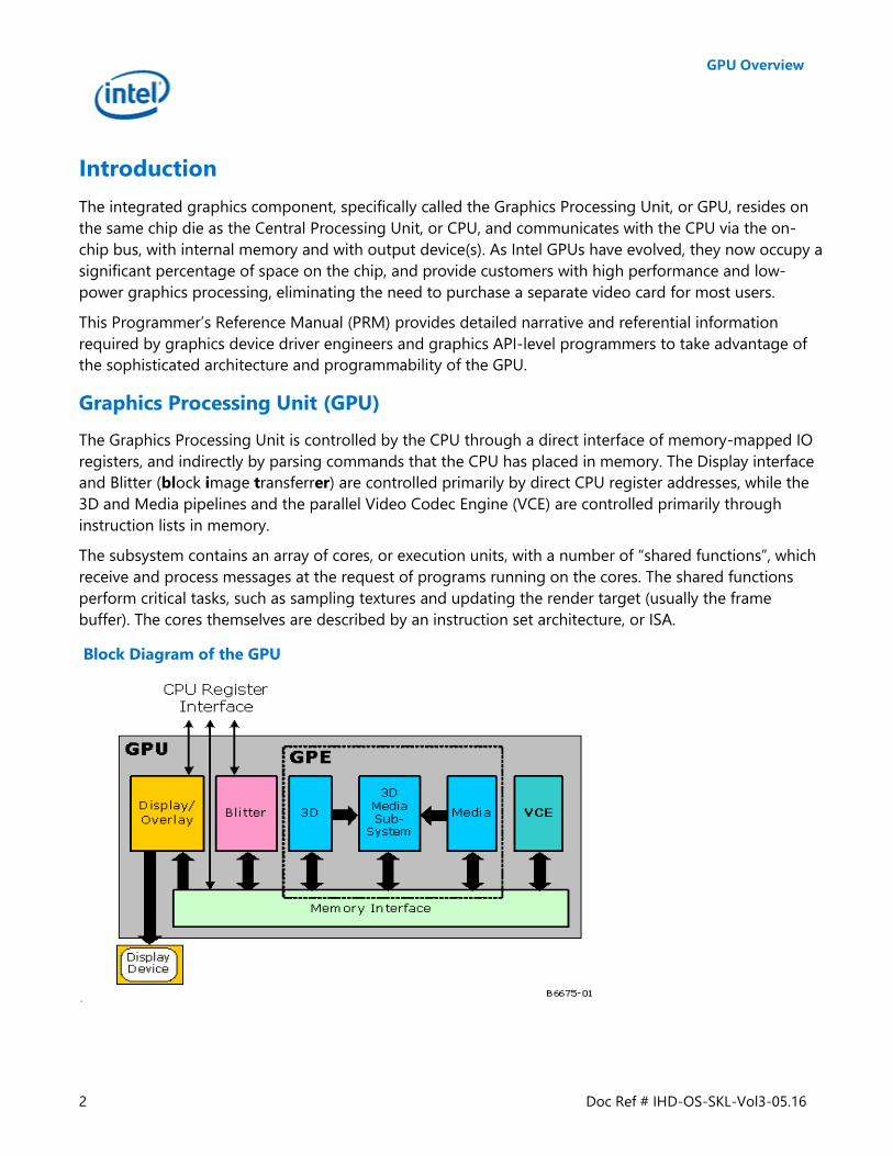
Introduction
The integrated graphics component, specifically called the Graphics Processing Unit, or GPU, resides on
the same chip die as the Central Processing Unit, or CPU, and communicates with the CPU via the on-
chip bus, with internal memory and with output device(s). As Intel GPUs have evolved, they now occupy a
significant percentage of space on the chip, and provide customers with high performance and low-
power graphics processing, eliminating the need to purchase a separate video card for most users.
This Programmer’s Reference Manual (PRM) provides detailed narrative and referential information
required by graphics device driver engineers and graphics API-level programmers to take advantage of
the sophisticated architecture and programmability of the GPU.
Graphics Processing Unit (GPU)
The Graphics Processing Unit is controlled by the CPU through a direct interface of memory-mapped IO
registers, and indirectly by parsing commands that the CPU has placed in memory. The Display interface
and Blitter (block image transferrer) are controlled primarily by direct CPU register addresses, while the
3D and Media pipelines and the parallel Video Codec Engine (VCE) are controlled primarily through
instruction lists in memory.
The subsystem contains an array of cores, or execution units, with a number of “shared functions”, which
receive and process messages at the request of programs running on the cores. The shared functions
perform critical tasks, such as sampling textures and updating the render target (usually the frame
buffer). The cores themselves are described by an instruction set architecture, or ISA.
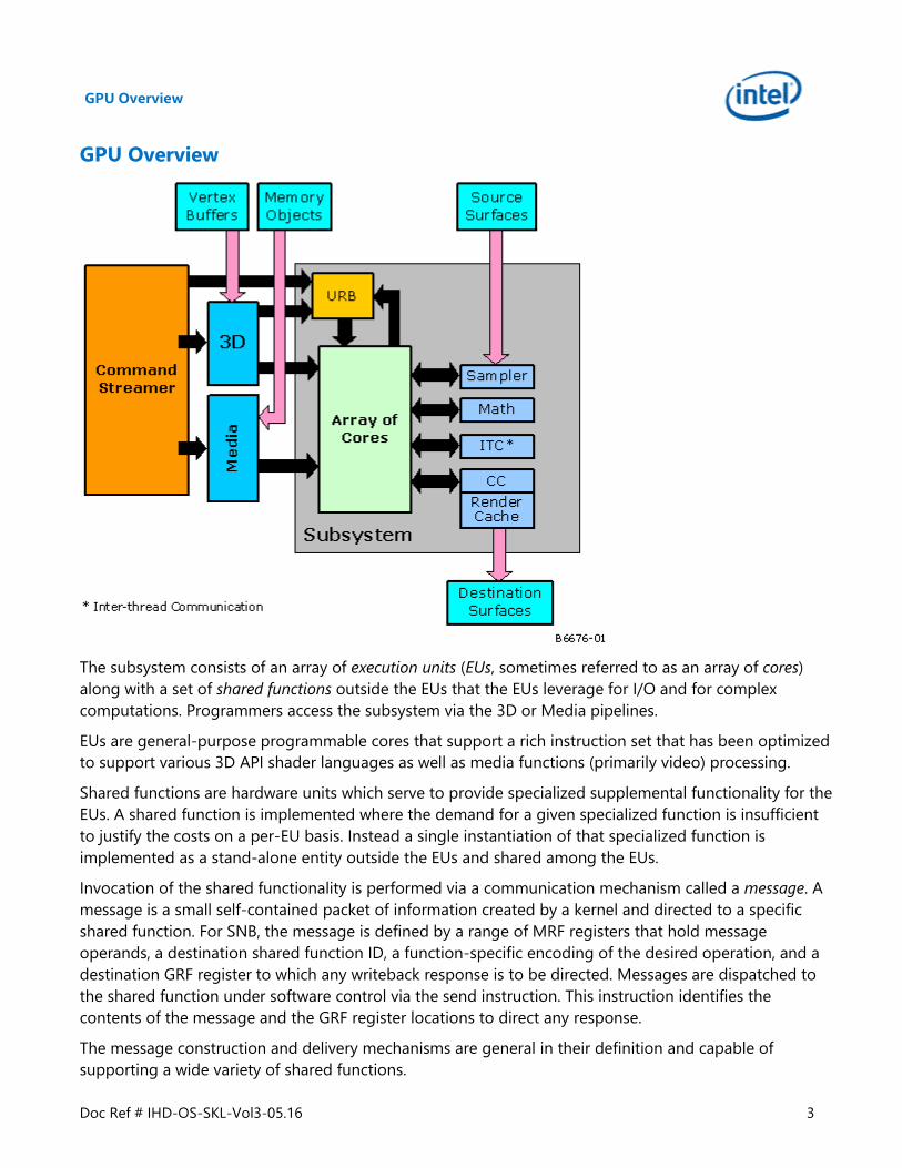
Block Diagram of the GPU
Page 6
GPU Overview
Doc Ref # IHD-OS-SKL-Vol3-05.16 3
GPU Overview
The subsystem consists of an array of execution units (EUs, sometimes referred to as an array of cores)
along with a set of shared functions outside the EUs that the EUs leverage for I/O and for complex
computations. Programmers access the subsystem via the 3D or Media pipelines.
EUs are general-purpose programmable cores that support a rich instruction set that has been optimized
to support various 3D API shader languages as well as media functions (primarily video) processing.
Shared functions are hardware units which serve to provide specialized supplemental functionality for the
EUs. A shared function is implemented where the demand for a given specialized function is insufficient
to justify the costs on a per-EU basis. Instead a single instantiation of that specialized function is
implemented as a stand-alone entity outside the EUs and shared among the EUs.
Invocation of the shared functionality is performed via a communication mechanism called a message. A
message is a small self-contained packet of information created by a kernel and directed to a specific
shared function. For SNB, the message is defined by a range of MRF registers that hold message
operands, a destination shared function ID, a function-specific encoding of the desired operation, and a
destination GRF register to which any writeback response is to be directed. Messages are dispatched to
the shared function under software control via the send instruction. This instruction identifies the
contents of the message and the GRF register locations to direct any response.
The message construction and delivery mechanisms are general in their definition and capable of
supporting a wide variety of shared functions.
Page 7
GPU Overview
4 Doc Ref # IHD-OS-SKL-Vol3-05.16
Command Stream (CS) Unit
The Command Stream (CS) unit manages the use of the 3D and Media pipelines; it performs switching
between pipelines and forwarding command streams to the currently active pipeline. It manages
allocation of the URB and helps support the Constant URB Entry (CURBE) function.
3D Pipeline
The 3D Pipeline provides specialized 3D primitive processing functions. These functions are provided by
a pipeline of “fixed function” stages (units) and GEN threads spawned by these units. See 3D Pipeline
Overview.
Media Pipeline
The Media pipeline provides both specialized media-related processing functions and the ability to
perform more general (“generic”) functionality. These Media-specific functions are provided by a Video
Front End (VFE) unit. A Thread Spawner (TS) unit is utilized to spawn GEN threads requested by the VFE
unit, or as required when the pipeline is used for general processing. See Media Pipeline Overview.
Thread Dispatching
When the 3D and Media pipelines send requests for thread initiation to the Subsystem, the thread
Dispatcher receives the requests. The dispatcher performs such tasks as arbitrating between concurrent
requests, assigning requested threads to hardware threads on EUs, allocating register space in each EU
among multiple threads, and initializing a thread’s registers with data from the fixed functions and from
the URB. This operation is largely transparent to software.
Execution Units (EUs)
The Execution Units (EUs) are the programmable shader units of the Gen Architecture. Each is a stand-
alone programmable computational unit used for execution of 3D shaders and media/gpgpu kernels.
Internally each is capable of multi-issue SIMD execution, and their hardware multi-threaded operation
provides a very high-efficiency execution environment in the face of long data latencies typically
associated with memory accesses. Each hardware thread within an EU has a dedicated large-capacity
high-bandwidth register file (GRF) and associated independent thread-state. Execution is multi-issue per
clock to pipelines capable of integer, single and double precision floating point operations, SIMD branch
capability, logical operations, transcendental operations, and other miscellaneous operations.
Communication to support units (shared functions) for operations such as texture sampling or
scatter/gather load/stores is via ‘messages’ programmatically constructed and ‘sent’ to those functions,
with dependency hardware causing the issuing thread to sleep until the requested data has been
returned.
EU instance count varies by product generation, as well as by SKU within a given generation, and their
capabilities have evolved over the many generation of the Gen Architecture.. Please see “Device
Attributes” in the “Configuration” chapter for specific rates and capacities associated with Execution
Units.
Page 8
GPU Overview
Doc Ref # IHD-OS-SKL-Vol3-05.16 5
Shared Functions
Shared functions are hardware units that provide specialized supplemental functionality for the EUs. A
shared function is implemented where the demand for a given specialized function is insufficient to
justify the costs on a per-EU basis. Instead a single instantiation of that specialized function is
implemented as a stand-alone entity outside the EUs and shared among the EUs.
Invocation of the shared functionality is performed via a communication mechanism called a message. A
message is a small self-contained packet of information created by a kernel and directed to a specific
shared function.
Programming Note
Context: Communication mechanism in shared functions
The message is defined by a range of Message Register File (MRF) registers that hold message operands, a
destination shared function ID, a function-specific encoding of the desired operation, and a destination General
Register File (GRF) register to which any writeback response is directed.
Messages are dispatched to the shared function under software control via the send instruction. This
instruction identifies the contents of the message and the GRF register locations to direct any response.
The message construction and delivery mechanisms are general in their definition and capable of
supporting a wide variety of shared functions.
Page 9
GPU Overview
6 Doc Ref # IHD-OS-SKL-Vol3-05.16
Fixed and Shared Function IDs
The following table lists the assignments (encodings) of the Shared Function and Fixed Function IDs used
within the GPE. A Shared Function is a valid target of a message initiated via a send instruction. A Fixed
Function is an identifiable unit of the 3D or Media pipeline. Note that the Thread Spawner is both a
Shared Function and Fixed Function.
Function IDs
ID[3:0] SFID Shared Function FFID Fixed Function
0x0 SFID_NULL Null FFID_NULL Null
0x1 Reserved --- Reserved ---
0x2 SFID_SAMPLER Sampler Reserved ---
0x3 SFID_GATEWAY Message Gateway Reserved ---
0x4 SFID_DP_DC2 Data Cache Data Port2 FFID_HS Hull Shader
0x5 SFID_DP_RC Render Cache Data Port FFID_DS Domain Shader
0x6 SFID_URB URB Reserved ---
0x7 SFID_SPAWNER Thread Spawner FFID_SPAWNER Thread Spawner
0x8 SFID_VME Video Motion Estimation FFID_VFE Video Front End
0x9 SFID_DP_DCRO Data Cache Read Only Data Port FFID_VS Vertex Shader
0xA SFID_DP_DC0 Data Cache Data Port0 FFID_CS Command Stream
0xB SFID_PI Pixel Interpolator FFID_VF Vertex Fetch
0xC SFID_DP_DC1 Data Cache Data Port1 FFID_GS Geometry Shader
0xD SFID_CRE Check & Refinement Engine FFID_VFE Video Front End
0xE Reserved --- FFID_SF Strip/Fan Unit
0xF Reserved --- FFID_WM Windower/Masker Unit
Programming Note
Context: Shared Function ID
SFID_DP_DC1 is an extension of SFID_DP_DC0 to allow for for more messages types. They act as a single logical
entity.
Programming Note
Context: Shared Function ID
SFID_DP_DC1 , SFID_DP_DC2, and SFID_P_DC3 are extensions of SFID_DP_DC0 to allow for more messages types.
They act as a single logical entity.
Page 10
GPU Overview
Doc Ref # IHD-OS-SKL-Vol3-05.16 7
Register Address Maps
Graphics Register Address Map
This chapter provides address maps of the graphics controllers I/O and memory-mapped registers.
Individual register bit field descriptions are provided in the following chapters. PCI configuration address
maps and register bit descriptions are provided in the following chapter.
Memory and IO Space Registers
These are graphics MMIO ranges used for SKL. Note that this is only a subset of the complete definition
of the MMIO address space.
Range Start (Hex) Range End (Hex) Unit Owning the Range
00002000 00002FFF Render/Generic Media Engine
00004000 00004FFF Render/Generic Media Graphics Memory Arbiter
00012000 000123FF MFX Control Engine (Video Command Streamer)
00012400 00012FFF Media Units (VIN Unit)
00014000 00014FFF MFX Memory Arbiter
00022000 00022FFF Blitter Engine
00024000 00024FFF Blitter Memory Arbiter
00100000 00107FFF Fence Registers
00140000 0017FFFF MCHBAR (SA)
Programming Note
Context: Memory and IO space registers, graphics MMIO ranges
8800h-88FFh is a reserved range for GT. IA accesses to this region have no impact.
VGA and Extended VGA Register Map
For I/O locations, the value in the address column represents the register I/O address. For memory
mapped locations, this address is an offset from the base address programmed in the MMADR register.
Page 11
GPU Overview
8 Doc Ref # IHD-OS-SKL-Vol3-05.16
VGA and Extended VGA I/O and Memory Register Map
Address Register Name (Read) Register Name (Write)
2D Registers
3B0h–3B3h Reserved Reserved
3B4h VGA CRTC Index (CRX)
(monochrome)
VGA CRTC Index (CRX) (monochrome)
3B5h VGA CRTC Data (monochrome) VGA CRTC Data (monochrome)
3B6h–3B9h Reserved Reserved
3Bah VGA Status Register (ST01) VGA Feature Control Register (FCR)
3BBh–3BFh Reserved Reserved
3C0h VGA Attribute Controller Index
(ARX)
VGA Attribute Controller Index (ARX)/
VGA Attribute Controller Data (alternating writes select ARX or
write ARxx Data)
3C1h VGA Attribute Controller Data
(read ARxx data)
Reserved
3C2h VGA Feature Read Register (ST00) VGA Miscellaneous Output Register (MSR)
3C3h Reserved Reserved
3C4h VGA Sequencer Index (SRX) VGA Sequencer Index (SRX)
3C5h VGA Sequencer Data (SRxx) VGA Sequencer Data (SRxx)
3C6h VGA Color Palette Mask (DACMASK) VGA Color Palette Mask (DACMASK)
3C7h VGA Color Palette State (DACSTATE) VGA Color Palette Read Mode Index (DACRX)
3C8h VGA Color Palette Write Mode
Index (DACWX)
VGA Color Palette Write Mode Index (DACWX)
3C9h VGA Color Palette Data (DACDATA) VGA Color Palette Data (DACDATA)
3CAh VGA Feature Control Register (FCR) Reserved
3CBh Reserved Reserved
3CCh VGA Miscellaneous Output Register
(MSR)
Reserved
3CDh Reserved Reserved
3CEh VGA Graphics Controller Index
(GRX)
VGA Graphics Controller Index (GRX)
3CFh VGA Graphics Controller Data
(GRxx)
VGA Graphics Controller Data (GRxx)
3D0h–3D1h Reserved Reserved
2D Registers
3D4h VGA CRTC Index (CRX) VGA CRTC Index (CRX)
3D5h VGA CRTC Data (CRxx) VGA CRTC Data (CRxx)
System Configuration Registers
Page 12
GPU Overview
Doc Ref # IHD-OS-SKL-Vol3-05.16 9
Address Register Name (Read) Register Name (Write)
3D6h GFX/2D Configurations Extensions
Index (XRX)
GFX/2D Configurations Extensions Index (XRX)
3D7h GFX/2D Configurations Extensions
Data (XRxx)
GFX/2D Configurations Extensions Data (XRxx)
2D Registers
3D8h–3D9h Reserved Reserved
3DAh VGA Status Register (ST01) VGA Feature Control Register (FCR)
3DBh–3DFh Reserved Reserved
Indirect VGA and Extended VGA Register Indices
The registers listed in this section are indirectly accessed by programming an index value into the
appropriate SRX, GRX, ARX, or CRX register. The index and data register address locations are listed in
the previous section. Additional details concerning the indirect access mechanism are provided in the
VGA and Extended VGA Register Description Chapter (see SRxx, GRxx, ARxx or CRxx sections).
2D Sequence Registers (3C4h / 3C5h)
Index Sym Description
00h SR00 Sequencer Reset
01h SR01 Clocking Mode
02h SR02 Plane / Map Mask
03h SR03 Character Font
04h SR04 Memory Mode
07h SR07 Horizontal Character Counter Reset
2D Graphics Controller Registers (3CEh / 3CFh)
Index Sym Register Name
00h GR00 Set / Reset
01h GR01 Enable Set / Reset
02h GR02 Color Compare
03h GR03 Data Rotate
04h GR04 Read Plane Select
05h GR05 Graphics Mode
06h GR06 Miscellaneous
07h GR07 Color Don’t Care
08h GR08 Bit Mask
10h GR10 Address Mapping
11h GR11 Page Selector
Page 13
GPU Overview
10 Doc Ref # IHD-OS-SKL-Vol3-05.16
Index Sym Register Name
18h GR18 Software Flags
2D Attribute Controller Registers (3C0h / 3C1h)
Index Sym Register Name
00h AR00 Palette Register 0
01h AR01 Palette Register 1
02h AR02 Palette Register 2
03h AR03 Palette Register 3
04h AR04 Palette Register 4
05h AR05 Palette Register 5
06h AR06 Palette Register 6
07h AR07 Palette Register 7
08h AR08 Palette Register 8
09h AR09 Palette Register 9
0Ah AR0A Palette Register A
0Bh AR0B Palette Register B
0Ch AR0C Palette Register C
0Dh AR0D Palette Register D
0Eh AR0E Palette Register E
0Fh AR0F Palette Register F
10h AR10 Mode Control
11h AR11 Overscan Color
12h AR12 Memory Plane Enable
13h AR13 Horizontal Pixel Panning
14h AR14 Color Select
2D CRT Controller Registers (3B4h / 3D4h / 3B5h / 3D5h)
Index Sym Register Name
00h CR00 Horizontal Total
01h CR01 Horizontal Display Enable End
02h CR02 Horizontal Blanking Start
03h CR03 Horizontal Blanking End
04h CR04 Horizontal Sync Start
05h CR05 Horizontal Sync End
06h CR06 Vertical Total
07h CR07 Overflow
Page 14
GPU Overview
Doc Ref # IHD-OS-SKL-Vol3-05.16 11
Index Sym Register Name
08h CR08 Preset Row Scan
09h CR09 Maximum Scan Line
0Ah CR0A Text Cursor Start
0Bh CR0B Text Cursor End
0Ch CR0C Start Address High
0Dh CR0D Start Address Low
0Eh CR0E Text Cursor Location High
0Fh CR0F Text Cursor Location Low
10h CR10 Vertical Sync Start
11h CR11 Vertical Sync End
12h CR12 Vertical Display Enable End
13h CR13 Offset
14h CR14 Underline Location
15h CR15 Vertical Blanking Start
16h CR16 Vertical Blanking End
17h CR17 CRT Mode
18h CR18 Line Compare
22h CR22 Memory Read Latch Data
Page 15
GPU Overview
12 Doc Ref # IHD-OS-SKL-Vol3-05.16
Memory Object Overview
Any memory data accessed by the device is considered part of a memory object of some memory object
type.
The following table lists the various memory objects types and an indication of their role in the system.
Memory Object Type Role
Graphics Translation
Table (GTT)
Contains PTEs used to translate "graphics addresses" into physical memory addresses.
Hardware Status Page Cached page of sysmem used to provide fast driver synchronization.
Logical Context Buffer Memory areas used to store (save/restore) images of hardware rendering contexts.
Logical contexts are referenced via a pointer to the corresponding Logical Context Buffer.
Ring Buffers Buffers used to transfer (DMA) instruction data to the device. Primary means of
controlling rendering operations.
Batch Buffers Buffers of instructions invoked indirectly from Ring Buffers.
State Descriptors Contains state information in a prescribed layout format to be read by hardware. Many
different state descriptor formats are supported.
Vertex Buffers Buffers of 3D vertex data indirectly referenced through "indexed" 3D primitive
instructions.
VGA Buffer
(Must be mapped UC
on PCI)
Graphics memory buffer used to drive the display output while in legacy VGA mode.
Display Surface Memory buffer used to display images on display devices.
Overlay Surface Memory buffer used to display overlaid images on display devices.
Overlay Register, Filter
Coefficients
Memory area used to provide double-buffer for Overlay register and filter coefficient
loading.
Cursor Surface Hardware cursor pattern in memory.
2D Render Source Surface used as primary input to 2D rendering operations.
2D Render R-M-W
Destination
2D rendering output surface that is read in order to be combined in the rendering
function. Destination surfaces that accessed via this Read-Modify-Write mode have
somewhat different restrictions than Write-Only Destination surfaces.
2D Render Write-Only
Destination
2D rendering output surface that is written but not read by the 2D rendering function.
Destination surfaces that accessed via a Write-Only mode have somewhat different
restrictions than Read-Modify-Write Destination surfaces.
2D Monochrome
Source
1 bpp surfaces used as inputs to 2D rendering after being converted to
foreground/background colors.
2D Color Pattern 8x8 pixel array used to supply the "pattern" input to 2D rendering functions.
DIB "Device Independent Bitmap" surface containing "logical" pixel values that are converted
(via LUTs) to physical colors.
3D Color Buffer Surface receiving color output of 3D rendering operations. May also be accessed via R-M-
W (aka blending). Also referred to as a Render Target.
Page 16
GPU Overview
Doc Ref # IHD-OS-SKL-Vol3-05.16 13
Memory Object Type Role
3D Depth Buffer Surface used to hold per-pixel depth and stencil values used in 3D rendering operations.
Accessed via RMW.
3D Texture Map Color surface (or collection of surfaces) which provide texture data in 3D rendering
operations.
"Non-3D" Texture Surface read by Texture Samplers, though not in normal 3D rendering operations (for
example, in video color conversion functions).
Motion Comp Surfaces These are the Motion Comp reference pictures.
Motion Comp
Correction Data Buffer
This is Motion Comp intra-coded or inter-coded correction data.
Hardware Status Page
The hardware status page is a naturally-aligned 4KB page residing in snooped system memory. This page
exists primarily to allow the device to report status via PCI master writes – thereby allowing the driver to
read/poll WB memory instead of UC reads of device registers or UC memory.
The address of this page is programmed via the HWS_PGA MI register. The definition of that register (in
Memory Interface Registers) includes a description of the layout of the Hardware Status Page.
Memory Access Indirection
The GPE supports the indirection of certain graphics (GTT-mapped) memory accesses. This support
comes in the form of two base address state variables used in certain memory address computations with
the GPE.
The intent of this functionality is to support the dynamic relocation of certain driver-generated memory
structures after command buffers have been generated but prior to their submittal for execution. For
example, as the driver builds the command stream it could append pipeline state descriptors, kernel
binaries, etc. to a general state buffer. References to the individual items would be inserted in the
command buffers as offsets from the base address of the state buffer. The state buffer could then be
freely relocated prior to command buffer execution, with the driver only needing to specify the final base
address of the state buffer. Two base addresses are provided to permit surface-related state (binding
tables, surface state tables) to be maintained in a state buffer separate from the general state buffer.
While the use of these base addresses is unconditional, the indirection can be effectively disabled by
setting the base addresses to zero. The following table lists the various GPE memory access paths and
which base address (if any) is relevant.
Page 17
GPU Overview
14 Doc Ref # IHD-OS-SKL-Vol3-05.16
Base Address Utilization
Base Address Used Memory Accesses
General State Base
Address
DataPort Read/Write DataPort memory accesses resulting from ‘stateless’ DataPort
Read/Write requests. See DataPort for a definition of the ‘stateless’ form of requests.
Dynamic State Base
Address
Sampler reads of SAMPLER_STATE data and associated SAMPLER_BORDER_COLOR_STATE.
Viewport states used by CLIP, SF, and WM/CC
COLOR_CALC_STATE, DEPTH_STENCIL_STATE, and BLEND_STATE
Push Constants (depending on state of INSTPM<CONSTANT_BUFFER Address Offset
Disable> )
Instruction Base
Address [SNB+]
Normal EU instruction stream (non-system routine)
System routine EU instruction stream (starting address = SIP)
Surface State Base
Address
Sampler and DataPort reads of BINDING_TABLE_STATE, as referenced by BT pointers passed
via 3DSTATE_BINDING_TABLE_POINTERS
Sampler and DataPort reads of SURFACE_STATE data
Indirect Object Base
Address
MEDIA_OBJECT Indirect Data accessed by the CS unit .
None CS unit reads from Ring Buffers, Batch Buffers
CS writes resulting from PIPE_CONTROL command
All VF unit memory accesses (Index Buffers, Vertex Buffers)
All Sampler Surface Memory Data accesses (texture fetch, etc.)
All DataPort memory accessesexcept ‘stateless’ DataPort Read/Write requests (e.g., RT
accesses.) See DataPort for a definition of the ‘stateless’ form of requests.
Memory reads resulting from STATE_PREFETCH commands
Any physical memory access by the device
GTT-mapped accesses not included above (i.e., default)
[SNB+]: Push Constants (depeding on state of INSTPM<CONSTANT_BUFFER Address
Offset Disable> )
The following notation is used in the PRM to distinguish between addresses and offsets:
Notation Definition
PhysicalAddress[n:m] Corresponding bits of a physical graphics memory byte address (not mapped by a GTT)
GraphicsAddress[n:m] Corresponding bits of an absolute, virtual graphics memory byte address (mapped by a
GTT)
GeneralStateOffset[n:m] Corresponding bits of a relative byte offset added to the General State Base Address
value, the result of which is interpreted as a virtual graphics memory byte address
(mapped by a GTT)
DynamicStateOffset[n:m] Corresponding bits of a relative byte offset added to the Dynamic State Base Address
value, the result of which is interpreted as a virtual graphics memory byte address
(mapped by a GTT)
Page 18
GPU Overview
Doc Ref # IHD-OS-SKL-Vol3-05.16 15
Notation Definition
InstructionBaseOffset[n:m] Corresponding bits of a relative byte offset added to the Instruction Base Address value,
the result of which is interpreted as a virtual graphics memory byte address (mapped by
a GTT)
SurfaceStateOffset[n:m] Corresponding bits of a relative byte offset added to the Surface State Base Address
value, the result of which is interpreted as a virtual graphics memory byte address
(mapped by a GTT)
Instruction Ring Buffers
Instruction ring buffers are the memory areas used to pass instructions to the device. Refer to the
Programming Interface chapter for a description of how these buffers are used to transport instructions.
The RINGBUF register sets (defined in Memory Interface Registers) are used to specify the ring buffer
memory areas. The ring buffer must start on a 4KB boundary and be allocated in linear memory. The
length of any one ring buffer is limited to 2MB.
Programming Note
Context: Instruction Ring Buffers in memory areas.
“Indirect” 3D primitive instructions (those that access vertex buffers) must reside in the same memory space as the
vertex buffers.
Instruction Batch Buffers
Instruction batch buffers are contiguous streams of instructions referenced via an
MI_BATCH_BUFFER_START and related instructions (see Memory Interface Instructions, Programming
Interface). They are used to transport instructions external to ring buffers.
Programming Note
Context: Instruction batch buffers in memory objects
Batch buffers should not be mapped to snooped SM (PCI) addresses. The device will treat these as MainMemory
(MM) addresses and, therefore, not snoop the CPU cache.
Programming Note
Context: Instruction batch buffers in memory objects
The batch buffer must be QWord aligned and a multiple of QWords in length. The ending address is the address of
the last valid QWord in the buffer. The length of any single batch buffer is “virtually unlimited” (i.e., could
theoretically be 4GB in length).
Page 19
GPU Overview
16 Doc Ref # IHD-OS-SKL-Vol3-05.16
Logical Contexts
This section is the lead section for the following subsections:
BSD Logical Render Context Address (LRCA)
Video Enhancement Logical Context Data
Logical Contexts
BSD Logical Render Context Address (LRCA)
This section discusses the following topics for the BSD Logical Render Context Address (LRCA):
Overall Context Layout
Register State Context
Ring Buffer
Ring Context
The Per-Process Hardware Status Page
Video Engine Power Context
Overall Context Layout
When Execlists are enabled, the Context Image for the media engine consists of two 4K pages:
Per-Process HW Status Page (4K)
Register State Context
When Execlists are disabled (ring buffer mode of scheduling) there is no concept of context for
workloads submitted to the media engine, and hence there is no context image.
Register State context is explained in detail in the “Register State Context” Section.
Page 20
GPU Overview
Doc Ref # IHD-OS-SKL-Vol3-05.16 17
Register/State Context
EXECLIST CONTEXT
EXECLIST CONTEXT(PPGTT Base)
ENGINE CONTEXT
Description MMIO Offset/Command Unit # of DW Address Offset(Dword)
NOOP VCS 1 0
Load_Register_Immediate header 0x1100_101B VCS 1 0001
Context Control 0x12244 VCS 2 0002
Ring Head Pointer Register 0x12034 VCS 2 0004
Ring Tail Pointer Register 0x12030 VCS 2 0006
RING_BUFFER_START 0x12038 VCS 2 0008
RING_BUFFER_CONTROL 0x1203C VCS 2 000A
Batch Buffer Current Head Register (UDW) 0x12168 VCS 2 000C
Batch Buffer Current Head Register 0x12140 VCS 2 000E
Batch Buffer State Register 0x12110 VCS 2 0010
SECOND_BB_ADDR_UDW 0x1211C VCS 2 0012
SECOND_BB_ADDR 0x12114 VCS 2 0014
SECOND_BB_STATE 0x12118 VCS 2 0016
BB_PER_CTX_PTR 0x121C0 VCS 2 0018
VCS_INDIRECT_CTX 0x121C4 VCS 2 001A
VCS_INDIRECT_CTX_OFFSET 0x121C8 VCS 2 001C
NOOP VCS 2 001E
NOOP VCS 1 0020
Load_Register_Immediate header 0x1100_1011 VCS 1 0021
CTX_TIMESTAMP 0x123A8 VCS 2 0022
PDP3_UDW 0x1228C VCS 2 0024
PDP3_LDW 0x12288 VCS 2 0026
PDP2_UDW 0x12284 VCS 2 0028
PDP2_LDW 0x12280 VCS 2 002A
PDP1_UDW 0x1227C VCS 2 002C
PDP1_LDW 0x12278 VCS 2 002E
PDP0_UDW 0x12274 VCS 2 0030
PDP0_LDW 0x12270 VCS 2 0032
NOOP VCS 12 0034
NOOP VCS 16 0040
Page 21
GPU Overview
18 Doc Ref # IHD-OS-SKL-Vol3-05.16
Description MMIO Offset/Command Unit # of DW Address Offset(Dword)
NOOP VCS 1 0050
Load_Register_Immediate header 0x1100_1057 VCS 1 0051
EXCC 0x12028 VCS 2 0052
MI_MODE 0x1209C VCS 2 0054
INSTPM 0x120C0 VCS 2 0056
PR_CTR_CTL 0x12178 VCS 2 0058
PR_CTR_THRSH 0x1217C VCS 2 005A
TIMESTAMP Register (LSB) 0x12358 VCS 2 005C
BB_START_ADDR_UDW 0x12170 VCS 2 005E
BB_START_ADDR 0x12150 VCS 2 0060
BB_ADD_DIFF 0x12154 VCS 2 0062
BB_OFFSET 0x12158 VCS 2 0064
MI_PREDICATE_RESULT_1 0x1241C VCS 2 0066
CS_GPR (1-16) 0x12600 VCS 64 0068
IPEHR 0x12068 VCS 2 00A8
NOOP VCS 6 00AA
Ring Buffer
Ring Buffer can exist anywhere in memory mapped via Global GTT. Ring buffer details are mentioned in
the ring context area of LRCA (Ring Buffer - Start Address, Head Offset, Tail Pointer & Control Register) in
the Execution List mode of scheduling.
Programming Note
Context: Ring buffers - ring context area of LRCA
Ring Buffer registers are directly programmed in the Ring Buffer mode of scheduling.
Ring Context
Ring Context starts at 4K offset from LRCA. Ring context contains all the details that are needed to be
initialized by SW for submitting a context to HW for execution (Ring Buffer Details, Page Directory
Information, etc.). Ring context is five cachelines in size.
Programming Note
Context: Submitting a context to HW for execution.
The last cacheline of the ring context is specific for a given Engine and hence SW needs to populate it accordingly.
Ring Context comprises of the EXECLIST CONTEXT, EXECLIST CONTEXT (PPGTT Base) of the register state
context. In Ring Buffer mode of scheduling EXECLIST CONTEXT contents are save/restored as NOOPS by
HW.
Page 22
GPU Overview
Doc Ref # IHD-OS-SKL-Vol3-05.16 19
EXECLIST CONTEXT
EXECLIST CONTEXT(PPGTT Base)
The Per-Process Hardware Status
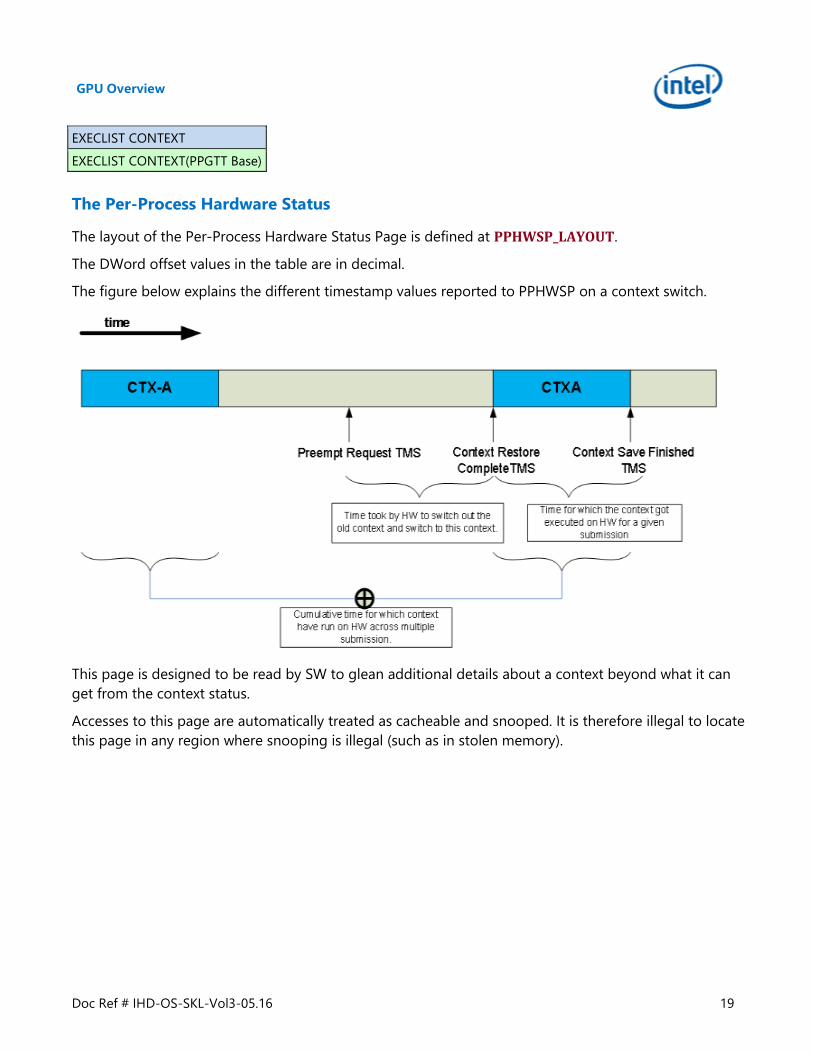
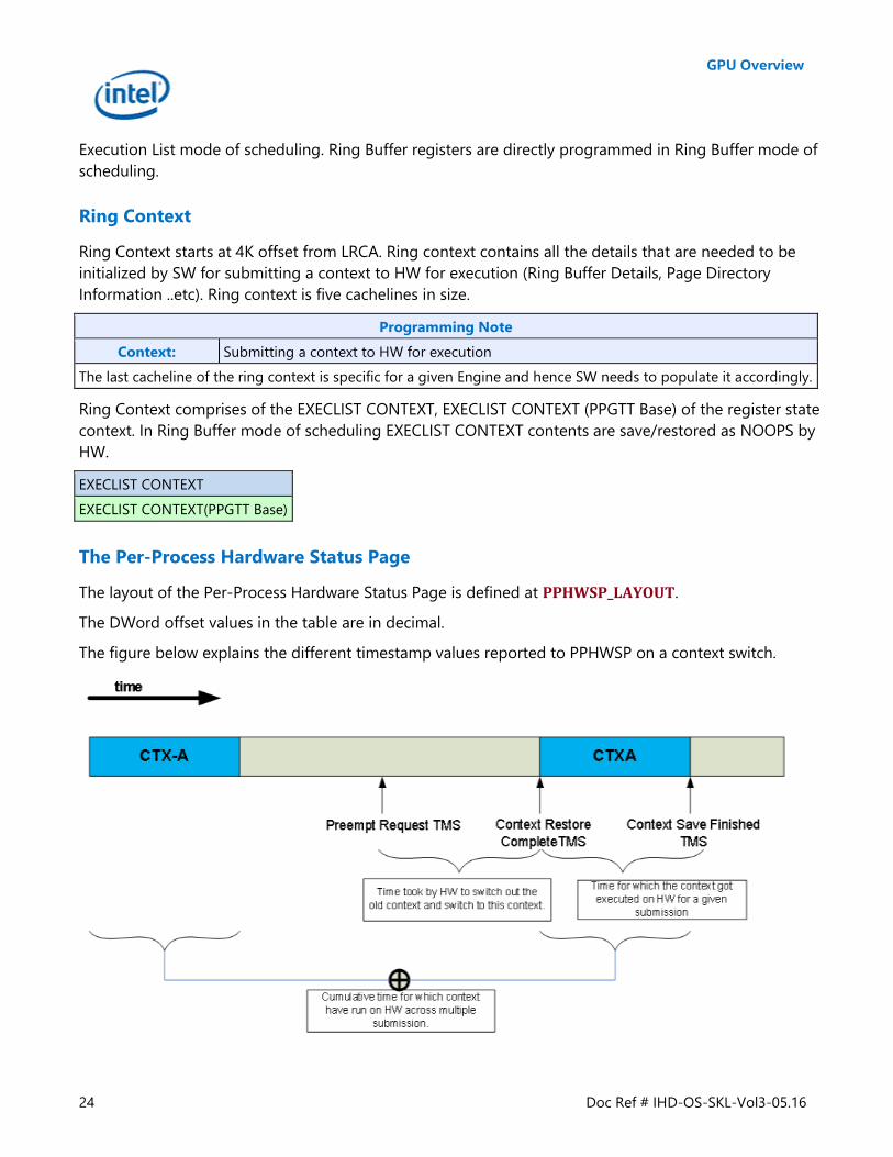
The layout of the Per-Process Hardware Status Page is defined at PPHWSP_LAYOUT.
The DWord offset values in the table are in decimal.
The figure below explains the different timestamp values reported to PPHWSP on a context switch.
This page is designed to be read by SW to glean additional details about a context beyond what it can
get from the context status.
Accesses to this page are automatically treated as cacheable and snooped. It is therefore illegal to locate
this page in any region where snooping is illegal (such as in stolen memory).
Page 23
GPU Overview
20 Doc Ref # IHD-OS-SKL-Vol3-05.16
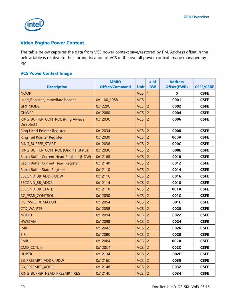
Video Engine Power Context
The table below captures the data from VCS power context save/restored by PM. Address offset in the
below table is relative to the starting location of VCS in the overall power context image managed by
PM.
VCS Power Context Image
Description
MMIO
Offset/Command Unit
# of
DW
Address
Offset(PWR) CSFE/CSBE
NOOP VCS 1 0 CSFE
Load_Register_Immediate header 0x1100_108B VCS 1 0001 CSFE
GFX_MODE 0x1229C VCS 2 0002 CSFE
GHWSP 0x12080 VCS 2 0004 CSFE
RING_BUFFER_CONTROL (Ring Always
Disabled )
0x1203C VCS 2 0006 CSFE
Ring Head Pointer Register 0x12034 VCS 2 0008 CSFE
Ring Tail Pointer Register 0x12030 VCS 2 000A CSFE
RING_BUFFER_START 0x12038 VCS 2 000C CSFE
RING_BUFFER_CONTROL (Original status) 0x1203C VCS 2 000E CSFE
Batch Buffer Current Head Register (UDW) 0x12168 VCS 2 0010 CSFE
Batch Buffer Current Head Register 0x12140 VCS 2 0012 CSFE
Batch Buffer State Register 0x12110 VCS 2 0014 CSFE
SECOND_BB_ADDR_UDW 0x1211C VCS 2 0016 CSFE
SECOND_BB_ADDR 0x12114 VCS 2 0018 CSFE
SECOND_BB_STATE 0x12118 VCS 2 001A CSFE
RC_PSMI_CONTROL 0x12050 VCS 2 001C CSFE
RC_PWRCTX_MAXCNT 0x12054 VCS 2 001E CSFE
CTX_WA_PTR 0x12058 VCS 2 0020 CSFE
NOPID 0x12094 VCS 2 0022 CSFE
HWSTAM 0x12098 VCS 2 0024 CSFE
IMR 0x120A8 VCS 2 0026 CSFE
EIR 0x120B0 VCS 2 0028 CSFE
EMR 0x120B4 VCS 2 002A CSFE
CMD_CCTL_0 0x120C4 VCS 2 002C CSFE
UHPTR 0x12134 VCS 2 002E CSFE
BB_PREEMPT_ADDR_UDW 0x1216C VCS 2 0030 CSFE
BB_PREEMPT_ADDR 0x12148 VCS 2 0032 CSFE
RING_BUFFER_HEAD_PREEMPT_REG 0x1214C VCS 2 0034 CSFE
Page 24
GPU Overview
Doc Ref # IHD-OS-SKL-Vol3-05.16 21
Description
MMIO
Offset/Command Unit
# of
DW
Address
Offset(PWR) CSFE/CSBE
PREEMPT_DLY 0x12214 VCS 2 0036 CSFE
SYNC_FLIP_STATUS 0x122D0 VCS 2 003A CSFE
SYNC_FLIP_STATUS_1 0x122D4 VCS 2 003C CSFE
SYNC_FLIP_STATUS_2 0x122EC VCS 2 003E CSFE
WAIT_FOR_RC6_EXIT 0x120CC VCS 2 0040 CSFE
RCS_CTXID_PREEMPTION_HINT 0x124CC VCS 2 0042 CSFE
CS_PREEMPTION_HINT_UDW 0x124C8 VCS 2 0044 CSFE
CS_PREEMPTION_HINT 0x124BC VCS 2 0046 CSFE
CCID Register 0x12180 VCS 2 0048 CSFE
SBB_PREEMPT_ADDRESS_UDW 0x12138 VCS 2 004A CSFE
SBB_PREEMPT_ADDRESS 0x1213C VCS 2 004C CSFE
MI_PREDICATE_RESULT_2 0x123BC VCS 2 004E CSFE
CTXT_ST_PTR 0x123A0 VCS 2 0050 CSFE
CTXT_ST_BUF 0x12370 VCS 24 0052 CSFE
SEMA_WAIT_POLL 0x1224C VCS 2 006A CSFE
IDLEDELAY 0x1223C VCS 2 006C CSFE
DISPLAY MESSAGE FORWARD STATUS 0x122E8 VCS 2 006E CSFE
RCS_FORCE_TO_NONPRIV 0x124D0 VCS 24 0070 CSFE
EXECLIST_STATUS_REGISTER 0x12234 VCS 2 0088 CSFE
CXT_OFFSET 0x21AC VCS 2 008C CSBE
NOOP 2 008C CSFE
NOOP VCS 1 008E CSBE
Load_Register_Immediate header 0x1100_1005 VCS 1 008F CSBE
GAC MODE REGISTER 0x120a0 VCS 2 0094 CSBE
NOOP VCS 6 0096 CSBE
NOOP VCS 1 009C CSBE
MI_BATCH_BUFFER_END VCS 1 009D CSBE
Page 25
GPU Overview
22 Doc Ref # IHD-OS-SKL-Vol3-05.16
Copy Engine Logical Context Data
Context Layout
When Execlists are enabled, the Context Image for the copy engine consists of two 4K pages:
Per-Process HW Status Page (4K)
Register State Context
When Execlists are disabled (ring buffer mode of scheduling) there is no concept of context for
workloads submitted to media engine and hence there is no context image.
Register State context is explained in detail in “Register State Context” Section.
Register/State Context
EXECLIST CONTEXT
EXECLIST CONTEXT(PPGTT Base)
ENGINE CONTEXT
Description MMIO Offset/Command Unit # of DW Address Offset(Dword)
NOOP BCS 1 0
Load_Register_Immediate header 0x1100_101B BCS 1 0001
Context Control 0x22244 BCS 2 0002
Ring Head Pointer Register 0x22034 BCS 2 0004
Ring Tail Pointer Register 0x22030 BCS 2 0006
RING_BUFFER_START 0x22038 BCS 2 0008
RING_BUFFER_CONTROL 0x2203C BCS 2 000A
Batch Buffer Current Head Register (UDW) 0x22168 BCS 2 000C
Batch Buffer Current Head Register 0x22140 BCS 2 000E
Batch Buffer State Register 0x22110 BCS 2 0010
SECOND_BB_ADDR_UDW 0x2211C BCS 2 0012
SECOND_BB_ADDR 0x22114 BCS 2 0014
SECOND_BB_STATE 0x22118 BCS 2 0016
BB_PER_CTX_PTR 0x221C0 BCS 2 0018
BCS_INDIRECT_CTX 0x221C4 BCS 2 001A
BCS_INDIRECT_CTX_OFFSET 0x221C8 BCS 2 001C
NOOP BCS 2 001E
NOOP BCS 1 0020
Load_Register_Immediate header 0x1100_1011 BCS 1 0021
CTX_TIMESTAMP 0x223A8 BCS 2 0022
Page 26
GPU Overview
Doc Ref # IHD-OS-SKL-Vol3-05.16 23
Description MMIO Offset/Command Unit # of DW Address Offset(Dword)
PDP3_UDW 0x2228C BCS 2 0024
PDP3_LDW 0x22288 BCS 2 0026
PDP2_UDW 0x22284 BCS 2 0028
PDP2_LDW 0x22280 BCS 2 002A
PDP1_UDW 0x2227C BCS 2 002C
PDP1_LDW 0x22278 BCS 2 002E
PDP0_UDW 0x22274 BCS 2 0030
PDP0_LDW 0x22270 BCS 2 0032
NOOP BCS 12 0034
NOOP BCS 1 0040
Load_Register_Immediate header 0x1100_0001 BCS 1 0041
BCS TILE REGISTER 0x22200 BCS 2 0042
NOOP BCS 12 0044
NOOP BCS 1 0050
Load_Register_Immediate header 0x1100_1057 BCS 1 0051
EXCC 0x22028 BCS 2 0052
MI_MODE 0x2209C BCS 2 0054
INSTPM 0x220C0 BCS 2 0056
PR_CTR_CTL 0x22178 BCS 2 0058
PR_CTR_THRSH 0x2217C BCS 2 005A
TIMESTAMP Register (LSB) 0x22358 BCS 2 005C
BB_START_ADDR_UDW 0x22170 BCS 2 005E
BB_START_ADDR 0x22150 BCS 2 0060
BB_ADD_DIFF 0x22154 BCS 2 0062
BB_OFFSET 0x22158 BCS 2 0064
MI_PREDICATE_RESULT_1 0x2241C BCS 2 0066
CS_GPR (1-16) 0x22600 BCS 64 0068
IPEHR 0x22068 BCS 2 00A8
NOOP BCS 6 00AA
DW 176
K Bytes 0.6875
Ring Buffer
Ring Buffer can exist anywhere in memory mapped via Global GTT. Ring buffer details are mentioned in
the ring context area of LRCA (Ring Buffer - Start Address, Head Offset, Tail Pointer & Control Register) in
Page 27
GPU Overview
24 Doc Ref # IHD-OS-SKL-Vol3-05.16
Execution List mode of scheduling. Ring Buffer registers are directly programmed in Ring Buffer mode of
scheduling.
Ring Context
Ring Context starts at 4K offset from LRCA. Ring context contains all the details that are needed to be
initialized by SW for submitting a context to HW for execution (Ring Buffer Details, Page Directory
Information ..etc). Ring context is five cachelines in size.
Programming Note
Context: Submitting a context to HW for execution
The last cacheline of the ring context is specific for a given Engine and hence SW needs to populate it accordingly.
Ring Context comprises of the EXECLIST CONTEXT, EXECLIST CONTEXT (PPGTT Base) of the register state
context. In Ring Buffer mode of scheduling EXECLIST CONTEXT contents are save/restored as NOOPS by
HW.
EXECLIST CONTEXT
EXECLIST CONTEXT(PPGTT Base)
The Per-Process Hardware Status Page
The layout of the Per-Process Hardware Status Page is defined at PPHWSP_LAYOUT.
The DWord offset values in the table are in decimal.
The figure below explains the different timestamp values reported to PPHWSP on a context switch.
Page 28
GPU Overview
Doc Ref # IHD-OS-SKL-Vol3-05.16 25
This page is designed to be read by SW to glean additional details about a context beyond what it can
get from the context status.
Accesses to this page are automatically treated as cacheable and snooped. It is therefore illegal to locate
this page in any region where snooping is illegal (such as in stolen memory).
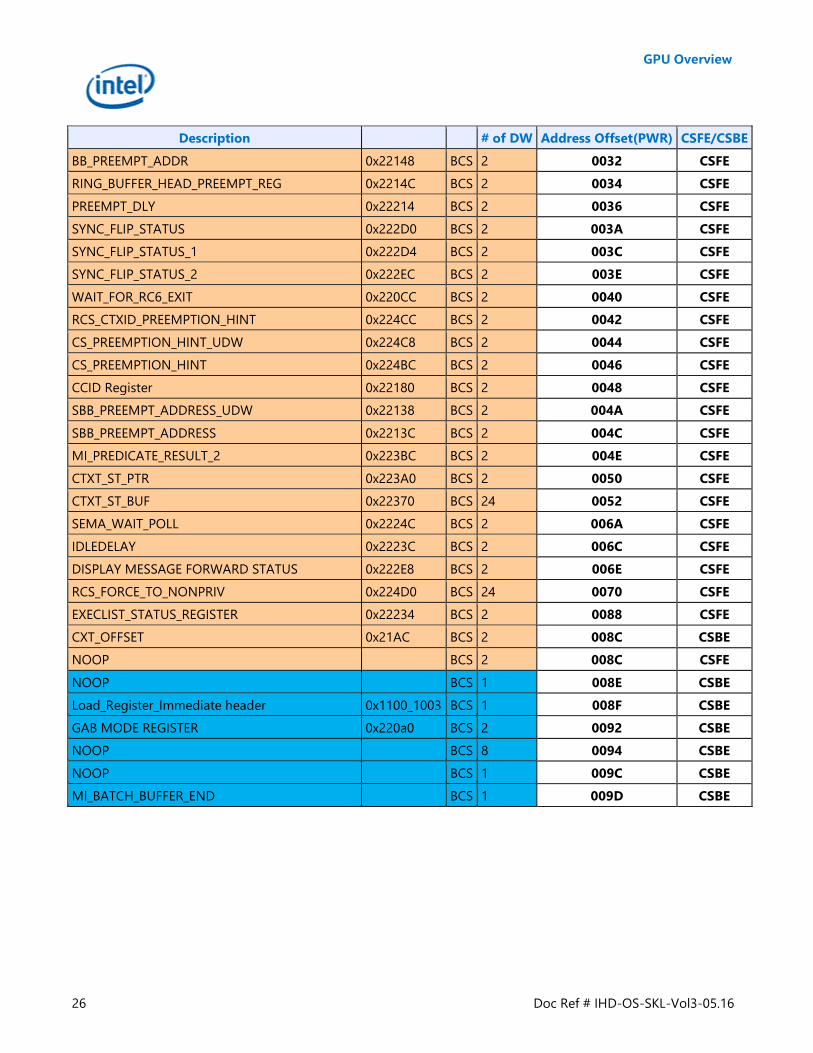
Blitter Engine Power Context
The table below captures the data from BCS power context save/restored by PM. Address offset in the
below table is relative to the starting location of BCS in the overall power context image managed by PM.
BCS Power Context Image
Description # of DW Address Offset(PWR) CSFE/CSBE
NOOP BCS 1 0 CSFE
Load_Register_Immediate header 0x1100_108B BCS 1 0001 CSFE
GFX_MODE 0x2229C BCS 2 0002 CSFE
GHWSP 0x22080 BCS 2 0004 CSFE
RING_BUFFER_CONTROL (Ring Always Disabled ) 0x2203C BCS 2 0006 CSFE
Ring Head Pointer Register 0x22034 BCS 2 0008 CSFE
Ring Tail Pointer Register 0x22030 BCS 2 000A CSFE
RING_BUFFER_START 0x22038 BCS 2 000C CSFE
RING_BUFFER_CONTROL (Original status) 0x2203C BCS 2 000E CSFE
Batch Buffer Current Head Register (UDW) 0x22168 BCS 2 0010 CSFE
Batch Buffer Current Head Register 0x22140 BCS 2 0012 CSFE
Batch Buffer State Register 0x22110 BCS 2 0014 CSFE
SECOND_BB_ADDR_UDW 0x2211C BCS 2 0016 CSFE
SECOND_BB_ADDR 0x22114 BCS 2 0018 CSFE
SECOND_BB_STATE 0x22118 BCS 2 001A CSFE
RC_PSMI_CONTROL 0x22050 BCS 2 001C CSFE
RC_PWRCTX_MAXCNT 0x22054 BCS 2 001E CSFE
CTX_WA_PTR 0x22058 BCS 2 0020 CSFE
NOPID 0x22094 BCS 2 0022 CSFE
HWSTAM 0x22098 BCS 2 0024 CSFE
IMR 0x220A8 BCS 2 0026 CSFE
EIR 0x220B0 BCS 2 0028 CSFE
EMR 0x220B4 BCS 2 002A CSFE
CMD_CCTL_0 0x220C4 BCS 2 002C CSFE
UHPTR 0x22134 BCS 2 002E CSFE
BB_PREEMPT_ADDR_UDW 0x2216C BCS 2 0030 CSFE
Page 29
GPU Overview
26 Doc Ref # IHD-OS-SKL-Vol3-05.16
Description # of DW Address Offset(PWR) CSFE/CSBE
BB_PREEMPT_ADDR 0x22148 BCS 2 0032 CSFE
RING_BUFFER_HEAD_PREEMPT_REG 0x2214C BCS 2 0034 CSFE
PREEMPT_DLY 0x22214 BCS 2 0036 CSFE
SYNC_FLIP_STATUS 0x222D0 BCS 2 003A CSFE
SYNC_FLIP_STATUS_1 0x222D4 BCS 2 003C CSFE
SYNC_FLIP_STATUS_2 0x222EC BCS 2 003E CSFE
WAIT_FOR_RC6_EXIT 0x220CC BCS 2 0040 CSFE
RCS_CTXID_PREEMPTION_HINT 0x224CC BCS 2 0042 CSFE
CS_PREEMPTION_HINT_UDW 0x224C8 BCS 2 0044 CSFE
CS_PREEMPTION_HINT 0x224BC BCS 2 0046 CSFE
CCID Register 0x22180 BCS 2 0048 CSFE
SBB_PREEMPT_ADDRESS_UDW 0x22138 BCS 2 004A CSFE
SBB_PREEMPT_ADDRESS 0x2213C BCS 2 004C CSFE
MI_PREDICATE_RESULT_2 0x223BC BCS 2 004E CSFE
CTXT_ST_PTR 0x223A0 BCS 2 0050 CSFE
CTXT_ST_BUF 0x22370 BCS 24 0052 CSFE
SEMA_WAIT_POLL 0x2224C BCS 2 006A CSFE
IDLEDELAY 0x2223C BCS 2 006C CSFE
DISPLAY MESSAGE FORWARD STATUS 0x222E8 BCS 2 006E CSFE
RCS_FORCE_TO_NONPRIV 0x224D0 BCS 24 0070 CSFE
EXECLIST_STATUS_REGISTER 0x22234 BCS 2 0088 CSFE
CXT_OFFSET 0x21AC BCS 2 008C CSBE
NOOP BCS 2 008C CSFE
NOOP BCS 1 008E CSBE
Load_Register_Immediate header 0x1100_1003 BCS 1 008F CSBE
GAB MODE REGISTER 0x220a0 BCS 2 0092 CSBE
NOOP BCS 8 0094 CSBE
NOOP BCS 1 009C CSBE
MI_BATCH_BUFFER_END BCS 1 009D CSBE
Page 30
GPU Overview
Doc Ref # IHD-OS-SKL-Vol3-05.16 27
Video Enhancement Logical Context Data
Context Layout
When Execlists are enabled, the Context Image for the Video Enhancement engine consists of two 4K
pages:
Per-Process HW Status Page (4K)
Register State Context
When Execlists are disabled (ring buffer mode of scheduling) there is no concept of context for
workloads submitted to media engine and hence there is no context image.
Register State context is explained in detail in the “Register State Context” Section.
Ring Context
Ring Context starts at 4K offset from LRCA. Ring context contains all the details that are needed to be
initialized by SW for submitting a context to HW for execution (Ring Buffer Details, Page Directory
Information ..etc). Ring context is five cachelines in size.
Programming Note
Context: Submitting a context to HW for execution
The last cacheline of the ring context is specific for a given Engine and hence SW needs to populate it accordingly.
Ring Context comprises of the EXECLIST CONTEXT, EXECLIST CONTEXT (PPGTT Base) of the register state
context. In Ring Buffer mode of scheduling EXECLIST CONTEXT contents are save/restored as NOOPS by
HW.
EXECLIST CONTEXT
EXECLIST CONTEXT(PPGTT Base)
Page 31
GPU Overview
28 Doc Ref # IHD-OS-SKL-Vol3-05.16
Register/State Context
EXECLIST CONTEXT
EXECLIST CONTEXT(PPGTT Base)
ENGINE CONTEXT
Description MMIO Offset/Command Unit
# of
DW
Address
Offset(Dword)
NOOP VECS 1 0
Load_Register_Immediate header 0x1100_101B VECS 1 0001
Context Control 0x1A244 VECS 2 0002
Ring Head Pointer Register 0x1A034 VECS 2 0004
Ring Tail Pointer Register 0x1A030 VECS 2 0006
RING_BUFFER_START 0x1A038 VECS 2 0008
RING_BUFFER_CONTROL 0x1A03C VECS 2 000A
Batch Buffer Current Head Register
(UDW)
0x1A168 VECS 2 000C
Batch Buffer Current Head Register 0x1A140 VECS 2 000E
Batch Buffer State Register 0x1A110 VECS 2 0010
SECOND_BB_ADDR_UDW 0x1A11C VECS 2 0012
SECOND_BB_ADDR 0x1A114 VECS 2 0014
SECOND_BB_STATE 0x1A118 VECS 2 0016
BB_PER_CTX_PTR 0x1A1C0 VECS 2 0018
VECS_INDIRECT_CTX 0x1A1C4 VECS 2 001A
VECS_INDIRECT_CTX_OFFSET 0x1A1C8 VECS 2 001C
NOOP VECS 2 001E
NOOP VECS 1 0020
Load_Register_Immediate header 0x1100_1011 VECS 1 0021
CTX_TIMESTAMP 0x1A3A8 VECS 2 0022
PDP3_UDW 0x1A28C VECS 2 0024
PDP3_LDW 0x1A288 VECS 2 0026
PDP2_UDW 0x1A284 VECS 2 0028
PDP2_LDW 0x1A280 VECS 2 002A
PDP1_UDW 0x1A27C VECS 2 002C
PDP1_LDW 0x1A278 VECS 2 002E
PDP0_UDW 0x1A274 VECS 2 0030
PDP0_LDW 0x1A270 VECS 2 0032
NOOP VECS 12 0034
Page 32
GPU Overview
Doc Ref # IHD-OS-SKL-Vol3-05.16 29
Description MMIO Offset/Command Unit
# of
DW
Address
Offset(Dword)
NOOP VECS 16 0040
NOOP VECS 1 0050
Load_Register_Immediate header 0x1100_1057 VECS 1 0051
EXCC 0x1A028 VECS 2 0052
MI_MODE 0x1A09C VECS 2 0054
INSTPM 0x1A0C0 VECS 2 0056
PR_CTR_CTL 0x1A178 VECS 2 0058
PR_CTR_THRSH 0x1A17C VECS 2 005A
TIMESTAMP Register (LSB) 0x1A358 VECS 2 005C
BB_START_ADDR_UDW 0x1A170 VECS 2 005E
BB_START_ADDR 0x1A150 VECS 2 0060
BB_ADD_DIFF 0x1A154 VECS 2 0062
BB_OFFSET 0x1A158 VECS 2 0064
MI_PREDICATE_RESULT_1 0x1A41C VECS 2 0066
CS_GPR (1-16) 0x1A600 VECS 64 0068
IPEHR 0x1A068 VECS 2 00A8
NOOP VECS 6 00AA
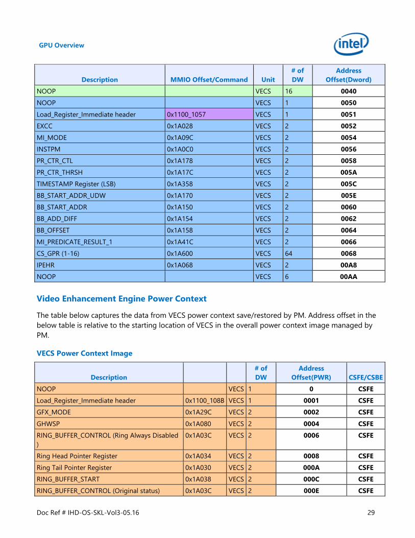
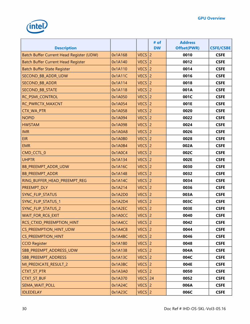
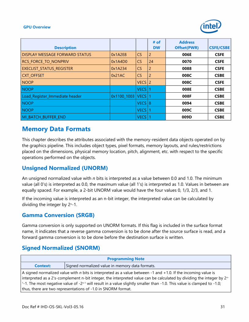
Video Enhancement Engine Power Context
The table below captures the data from VECS power context save/restored by PM. Address offset in the
below table is relative to the starting location of VECS in the overall power context image managed by
PM.
VECS Power Context Image
Description
# of
DW
Address
Offset(PWR) CSFE/CSBE
NOOP VECS 1 0 CSFE
Load_Register_Immediate header 0x1100_108B VECS 1 0001 CSFE
GFX_MODE 0x1A29C VECS 2 0002 CSFE
GHWSP 0x1A080 VECS 2 0004 CSFE
RING_BUFFER_CONTROL (Ring Always Disabled
)
0x1A03C VECS 2 0006 CSFE
Ring Head Pointer Register 0x1A034 VECS 2 0008 CSFE
Ring Tail Pointer Register 0x1A030 VECS 2 000A CSFE
RING_BUFFER_START 0x1A038 VECS 2 000C CSFE
RING_BUFFER_CONTROL (Original status) 0x1A03C VECS 2 000E CSFE
Page 33
GPU Overview
30 Doc Ref # IHD-OS-SKL-Vol3-05.16
Description
# of
DW
Address
Offset(PWR) CSFE/CSBE
Batch Buffer Current Head Register (UDW) 0x1A168 VECS 2 0010 CSFE
Batch Buffer Current Head Register 0x1A140 VECS 2 0012 CSFE
Batch Buffer State Register 0x1A110 VECS 2 0014 CSFE
SECOND_BB_ADDR_UDW 0x1A11C VECS 2 0016 CSFE
SECOND_BB_ADDR 0x1A114 VECS 2 0018 CSFE
SECOND_BB_STATE 0x1A118 VECS 2 001A CSFE
RC_PSMI_CONTROL 0x1A050 VECS 2 001C CSFE
RC_PWRCTX_MAXCNT 0x1A054 VECS 2 001E CSFE
CTX_WA_PTR 0x1A058 VECS 2 0020 CSFE
NOPID 0x1A094 VECS 2 0022 CSFE
HWSTAM 0x1A098 VECS 2 0024 CSFE
IMR 0x1A0A8 VECS 2 0026 CSFE
EIR 0x1A0B0 VECS 2 0028 CSFE
EMR 0x1A0B4 VECS 2 002A CSFE
CMD_CCTL_0 0x1A0C4 VECS 2 002C CSFE
UHPTR 0x1A134 VECS 2 002E CSFE
BB_PREEMPT_ADDR_UDW 0x1A16C VECS 2 0030 CSFE
BB_PREEMPT_ADDR 0x1A148 VECS 2 0032 CSFE
RING_BUFFER_HEAD_PREEMPT_REG 0x1A14C VECS 2 0034 CSFE
PREEMPT_DLY 0x1A214 VECS 2 0036 CSFE
SYNC_FLIP_STATUS 0x1A2D0 VECS 2 003A CSFE
SYNC_FLIP_STATUS_1 0x1A2D4 VECS 2 003C CSFE
SYNC_FLIP_STATUS_2 0x1A2EC VECS 2 003E CSFE
WAIT_FOR_RC6_EXIT 0x1A0CC VECS 2 0040 CSFE
RCS_CTXID_PREEMPTION_HINT 0x1A4CC VECS 2 0042 CSFE
CS_PREEMPTION_HINT_UDW 0x1A4C8 VECS 2 0044 CSFE
CS_PREEMPTION_HINT 0x1A4BC VECS 2 0046 CSFE
CCID Register 0x1A180 VECS 2 0048 CSFE
SBB_PREEMPT_ADDRESS_UDW 0x1A138 VECS 2 004A CSFE
SBB_PREEMPT_ADDRESS 0x1A13C VECS 2 004C CSFE
MI_PREDICATE_RESULT_2 0x1A3BC VECS 2 004E CSFE
CTXT_ST_PTR 0x1A3A0 VECS 2 0050 CSFE
CTXT_ST_BUF 0x1A370 VECS 24 0052 CSFE
SEMA_WAIT_POLL 0x1A24C VECS 2 006A CSFE
IDLEDELAY 0x1A23C VECS 2 006C CSFE
Page 34
GPU Overview
Doc Ref # IHD-OS-SKL-Vol3-05.16 31
Description
# of
DW
Address
Offset(PWR) CSFE/CSBE
DISPLAY MESSAGE FORWARD STATUS 0x1A2E8 CS 2 006E CSFE
RCS_FORCE_TO_NONPRIV 0x1A4D0 CS 24 0070 CSFE
EXECLIST_STATUS_REGISTER 0x1A234 CS 2 0088 CSFE
CXT_OFFSET 0x21AC CS 2 008C CSBE
NOOP VECS 2 008C CSFE
NOOP VECS 1 008E CSBE
Load_Register_Immediate header 0x1100_1003 VECS 1 008F CSBE
NOOP VECS 8 0094 CSBE
NOOP VECS 1 009C CSBE
MI_BATCH_BUFFER_END VECS 1 009D CSBE
Memory Data Formats
This chapter describes the attributes associated with the memory-resident data objects operated on by
the graphics pipeline. This includes object types, pixel formats, memory layouts, and rules/restrictions
placed on the dimensions, physical memory location, pitch, alignment, etc. with respect to the specific
operations performed on the objects.
Unsigned Normalized (UNORM)
An unsigned normalized value with n bits is interpreted as a value between 0.0 and 1.0. The minimum
value (all 0’s) is interpreted as 0.0, the maximum value (all 1’s) is interpreted as 1.0. Values in between are
equally spaced. For example, a 2-bit UNORM value would have the four values 0, 1/3, 2/3, and 1.
If the incoming value is interpreted as an n-bit integer, the interpreted value can be calculated by
dividing the integer by 2n-1.
Gamma Conversion (SRGB)
Gamma conversion is only supported on UNORM formats. If this flag is included in the surface format
name, it indicates that a reverse gamma conversion is to be done after the source surface is read, and a
forward gamma conversion is to be done before the destination surface is written.
Signed Normalized (SNORM)
Programming Note
Context: Signed normalized value in memory data formats.
A signed normalized value with n bits is interpreted as a value between -1 and +1.0. If the incoming value is
interpreted as a 2's-complement n-bit integer, the interpreted value can be calculated by dividing the integer by 2n-
1-1. The most negative value of -2n-1 will result in a value slightly smaller than -1.0. This value is clamped to -1.0;
thus, there are two representations of -1.0 in SNORM format.
Page 35
GPU Overview
32 Doc Ref # IHD-OS-SKL-Vol3-05.16
Unsigned Integer (UINT/USCALED)
The UINT and USCALED formats interpret the source as an unsigned integer value with n bits with a
range of 0 to 2n-1.
The UINT formats copy the source value to the destination (zero-extending if required), keeping the
value as an integer.
The USCALED formats convert the integer into the corresponding floating point value (e.g., 0x03 -->
3.0f). For 32-bit sources, the value is rounded to nearest even.
Signed Integer (SINT/SSCALED)
A signed integer value with n bits is interpreted as a 2’s complement integer with a range of -2n-1 to +2n-
1-1.
The SINT formats copy the source value to the destination (sign-extending if required), keeping the value
as an integer.
The SSCALED formats convert the integer into the corresponding floating point value (e.g., 0xFFFD --> -
3.0f). For 32-bit sources, the value is rounded to nearest even.
Floating Point (FLOAT)
Refer to IEEE Standard 754 for Binary Floating-Point Arithmetic. The IA-32 Intel (R) Architecture Software
Developer’s Manual also describes floating point data types .
64-bit Floating Point
Bit Description
63 Sign (s)
62:52 Exponent (e) Biased Exponent
51:0 Fraction (f) Does not include "hidden one"
The value of this data type is derived as:
if e == b’11..11’ and f != 0, then v is NaN regardless of s
if e == b’11..11’ and f == 0, then v = (-1)s*infinity (signed infinity)
if 0 < e < b’11..11’, then v = (-1)s*2(e-1023)*(1.f)
if e == 0 and f != 0, then v = (-1)s*2(e-1022)*(0.f) (denormalized numbers)
if e == 0 and f == 0, then v = (-1)s*0 (signed zero)
Page 36
GPU Overview
Doc Ref # IHD-OS-SKL-Vol3-05.16 33
32-bit Floating Point
Bit Description
31 Sign (s)
30:23 Exponent (e) Biased Exponent
22:0 Fraction (f) Does not include "hidden one"
The value of this data type is derived as:
if e == 255 and f != 0, then v is NaN regardless of s
if e == 255 and f == 0, then v = (-1)s*infinity (signed infinity)
if 0 < e < 255, then v = (-1)s*2(e-127)*(1.f)
if e == 0 and f != 0, then v = (-1)s*2(e-126)*(0.f) (denormalized numbers)
if e == 0 and f == 0, then v = (-1)s*0 (signed zero)
16-bit Floating Point
Bit Description
15 Sign (s)
14:10 Exponent (e) Biased Exponent
9:0 Fraction (f) Does not include "hidden one"
The value of this data type is derived as:
if e == 31 and f != 0, then v is NaN regardless of s
if e == 31 and f == 0, then v = (-1)s*infinity (signed infinity)
if 0 < e < 31, then v = (-1)s*2(e-15)*(1.f)
if e == 0 and f != 0, then v = (-1)s*2(e-14)*(0.f) (denormalized numbers)
if e == 0 and f == 0, then v = (-1)s*0 (signed zero)
The following table represents relationship between 32 bit and 16 bit floating point ranges:
flt32 exponent Unbiased exponent Normalization flt16 exponent flt16 fraction
255
254 127
...
127+16 16 Infinity 31 1.1111111111
127+15 15 Max exponent 30 1.xxxxxxxxxx
127 0 15 1.xxxxxxxxxx
113 -14 Min exponent 1 1.xxxxxxxxxx
112 Denormalized 0 0.1xxxxxxxxx
111 Denormalized 0 0.01xxxxxxxx
Page 37
GPU Overview
34 Doc Ref # IHD-OS-SKL-Vol3-05.16
flt32 exponent Unbiased exponent Normalization flt16 exponent flt16 fraction
110 Denormalized 0 0.001xxxxxxx
109 Denormalized 0 0.0001xxxxxx
108 Denormalized 0 0.00001xxxxx
107 Denormalized 0 0.000001xxxx
106 Denormalized 0 0.0000001xxx
115 Denormalized 0 0.00000001xx
114 Denormalized 0 0.000000001x
113 Denormalized 0 0.0000000001
112 Denormalized 0 0.0
...
0 0 0.0
Conversion from the 32-bit floating point format to the 16-bit format should be done with round to
nearest even.
11-bit Floating Point
Bits Description
10:6 Exponent (e): Biased exponent (the bias depends
on e)
5:0 Fraction (f): Fraction bits to the right of the binary
point
The value v of an 11-bit floating-point number is calculated from e and f as:
if e == 31 and f != 0 then v = NaN
if e == 31 and f == 0 then v = +infinity
if 0 < e < 31, then v = 2(e-15)*(1.f)
if e == 0 and f != 0, then v = 2(e-14)*(0.f) (denormalized numbers)
if e == 0 and f == 0, then v = 0 (zero)
There is no sign bit and negative values are not represented.
The 11-bit floating-point format has one more bit of fractional precision than the 10-bit floating-point
format.
The maximum representable finite value is 1.111111b * 215 = FE00h = 65024.
Page 38
GPU Overview
Doc Ref # IHD-OS-SKL-Vol3-05.16 35
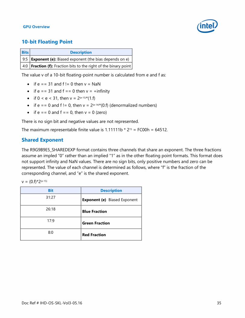
10-bit Floating Point
Bits Description
9:5 Exponent (e): Biased exponent (the bias depends on e)
4:0 Fraction (f): Fraction bits to the right of the binary point
The value v of a 10-bit floating-point number is calculated from e and f as:
if e == 31 and f != 0 then v = NaN
if e == 31 and f == 0 then v = +infinity
if 0 < e < 31, then v = 2(e-15)*(1.f)
if e == 0 and f != 0, then v = 2(e-14)*(0.f) (denormalized numbers)
if e == 0 and f == 0, then v = 0 (zero)
There is no sign bit and negative values are not represented.
The maximum representable finite value is 1.11111b * 215 = FC00h = 64512.
Shared Exponent
The R9G9B9E5_SHAREDEXP format contains three channels that share an exponent. The three fractions
assume an impled “0” rather than an implied “1” as in the other floating point formats. This format does
not support infinity and NaN values. There are no sign bits, only positive numbers and zero can be
represented. The value of each channel is determined as follows, where “f” is the fraction of the
corresponding channel, and “e” is the shared exponent.
v = (0.f)*2(e-15)
Bit Description
31:27 Exponent (e) Biased Exponent
26:18 Blue Fraction
17:9 Green Fraction
8:0 Red Fraction
Page 39
GPU Overview
36 Doc Ref # IHD-OS-SKL-Vol3-05.16
Memory Compression
Media Memory Compression
The software requirement when using media memory compression is to allocate each compressible
surface one memory tile wider than is required based on the surface width plus normal byte padding
(this approach is called “pitch+1”). The reason is each compressible surface needs an “extra” tile to the
right edge of surface to store important compression control information. For example, if the surface is
1920x1088, this would normally be allocated by the driver to be 2048 bytes wide, or 16 tiles (for NV12
8bpp). Using this “pitch + 1”, the pitch would be set to 17 instead of 16 (and the surface width remains
unchanged, only pitch is increased).
The largest supported width will be 4K pixels for 2D RGBA 8bpp surfaces and 2x2K for S3D surfaces (for
4KB pages). E.g. the pitch would be set to 129 in these cases (128+1). NV12 4K would be 33 (28+1). The
case of 64KB pages is the same: the driver will allocate 1 extra page to the right (“pitch + 1”), however
now the 4K wide restriction is relaxed. With 64KB pages, the widest surface that supports memory
compression is 16K for 2D RGBA 8bpp or 2x8K for S3D. E.g. the pitch would be set to 129 in these cases
(128+1).