2007-2014 Microchip Technology Inc. DS70000195F-page 1 HIGHLIGHTS This section of the manual contains the following major topics: 1.0 Introduction ....................................................................................................................... 2 2.0 I 2 C Bus Characteristics ..................................................................................................... 4 3.0 Control and Status Registers ............................................................................................ 8 4.0 Enabling I 2 C Operation ................................................................................................... 18 5.0 Communicating as a Master in a Single Master Environment ........................................ 20 6.0 Communicating as a Master in a Multi-Master Environment .......................................... 34 7.0 Communicating as a Slave ............................................................................................. 37 8.0 Connection Considerations for I 2 C Bus .......................................................................... 61 9.0 Operation in Power-Saving Modes ................................................................................. 63 10.0 Peripheral Module Disable (PMDx) Registers ................................................................ 63 11.0 Effects of a Reset ............................................................................................................ 63 12.0 Constant-Current Source ................................................................................................ 64 13.0 Register Maps ................................................................................................................. 66 14.0 Design Tips ..................................................................................................................... 67 15.0 Related Application Notes............................................................................................... 68 16.0 Revision History .............................................................................................................. 69 Inter-Integrated Circuit™ (I 2 C™)
Transcript
Inter-Integrated Circuit™ (I2C™)
HIGHLIGHTS
This section of the manual contains the following major topics:
15.0 Related Application Notes............................................................................................... 68
16.0 Revision History .............................................................................................................. 69
2007-2014 Microchip Technology Inc. DS70000195F-page 1
dsPIC33/PIC24 Family Reference Manual
This document supersedes the following PIC24 and dsPIC® DSC Family Reference Manual sections:
1.0 INTRODUCTION
The Inter-Integrated Circuit™ (I2C™) module is a serial interface useful for communicating withother peripheral or microcontroller (MCU) devices. The external peripheral devices may be serialEEPROMs, display drivers, Analog-to-Digital Converters (ADC) and so on.
The I2C module can operate as any one of the following in the I2C system:
• Slave device
• Master device in a single master system (slave may be active)
• Master or slave device in a multi-master system (bus collision detection and arbitration are available)
The I2C module contains an independent I2C master logic and a I2C slave logic, which generatesinterrupts based on their events. In the multi-master systems, the user software is simplypartitioned into the master controller and the slave controller.
When the I2C master logic is active, the slave logic also remains active, detecting the state of thebus and potentially receiving messages from itself in a single master system or from the othermasters in a multi-master system. No messages are lost during the multi-master bus arbitration.
In a multi-master system, the bus collision conflicts with the other masters in the system whendetected and the module provides a method to terminate and then restart the message.
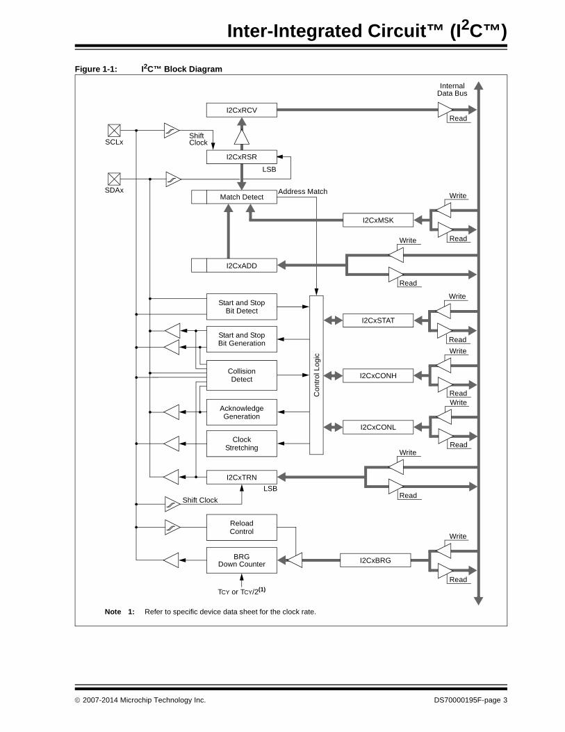
The I2C module contains a Baud Rate Generator (BRG). The I2C BRG does not consume othertimer resources in the device. Figure 1-1 illustrates the I2C module block diagram.
Key features of the I2C module include the following:
• Independent master and slave logic
• Multi-master support which prevents message losses in arbitration
• Detects 7-bit and 10-bit device addresses with configurable address masking in Slave mode
• Detects general call addresses as defined in the I2C protocol
• Bus Repeater mode allowing the module to accept all messages as a slave, irrespective of the address
• Automatic SCLx clock stretching provides delays for the processor to respond to a slave data request
• Supports 100 kHz and 400 kHz bus specifications
• Supports the Intelligent Platform Management Interface (IPMI) standard
• Supports SDAx hold time for SMBus (300 nS or 150 nS) in Slave mode
Note: This family reference manual section is meant to serve as a complement to devicedata sheets. Depending on the device variant, this manual section may not apply toall PIC24 and dsPIC33 devices.
Please consult the note at the beginning of the “Inter-Integrated Circuit™ (I2C™)”chapter in the current device data sheet to check whether this document supportsthe device you are using.
Device data sheets and family reference manual sections are available fordownload from the Microchip Worldwide Web site at: http://www.microchip.com.
DS Number Section Number Title
DS70195 19 dsPIC33F/PIC24H Family Reference Manual
DS70330 19 dsPIC33E/PIC24E Family Reference Manual
DS39702 24 PIC24F Family Reference Manual
DS70235 19 PIC24H Family Reference Manual
DS70068 21 dsPIC30F Family Reference Manual
Note: For more information, refer to the SDAHT bit description in the specific device data sheet.
DS70000195F-page 2 2007-2014 Microchip Technology Inc.
Note 1: Refer to specific device data sheet for the clock rate.
I2CxADD
Start and StopBit Detect
Start and StopBit Generation
CollisionDetect
I2CxMSK
2007-2014 Microchip Technology Inc. DS70000195F-page 3
dsPIC33/PIC24 Family Reference Manual
2.0 I2C BUS CHARACTERISTICS
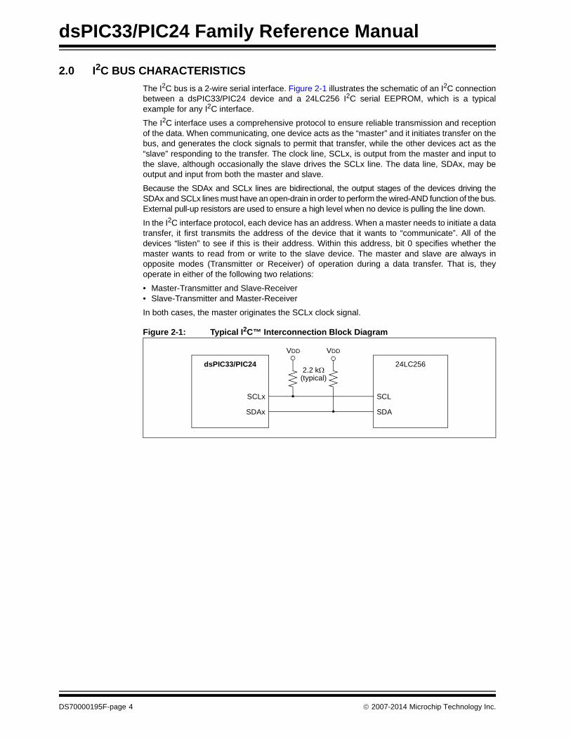
The I2C bus is a 2-wire serial interface. Figure 2-1 illustrates the schematic of an I2C connectionbetween a dsPIC33/PIC24 device and a 24LC256 I2C serial EEPROM, which is a typicalexample for any I2C interface.
The I2C interface uses a comprehensive protocol to ensure reliable transmission and receptionof the data. When communicating, one device acts as the “master” and it initiates transfer on thebus, and generates the clock signals to permit that transfer, while the other devices act as the“slave” responding to the transfer. The clock line, SCLx, is output from the master and input tothe slave, although occasionally the slave drives the SCLx line. The data line, SDAx, may beoutput and input from both the master and slave.
Because the SDAx and SCLx lines are bidirectional, the output stages of the devices driving theSDAx and SCLx lines must have an open-drain in order to perform the wired-AND function of the bus.External pull-up resistors are used to ensure a high level when no device is pulling the line down.
In the I2C interface protocol, each device has an address. When a master needs to initiate a datatransfer, it first transmits the address of the device that it wants to “communicate”. All of thedevices “listen” to see if this is their address. Within this address, bit 0 specifies whether themaster wants to read from or write to the slave device. The master and slave are always inopposite modes (Transmitter or Receiver) of operation during a data transfer. That is, theyoperate in either of the following two relations:
• Master-Transmitter and Slave-Receiver• Slave-Transmitter and Master-Receiver
In both cases, the master originates the SCLx clock signal.
DS70000195F-page 4 2007-2014 Microchip Technology Inc.
Inter-Integrated Circuit™ (I2C™)
2.1 Bus Protocol
The following I2C bus protocol has been defined:
• The data transfer may be initiated only when the bus is not busy.
• During the data transfer, the data line must remain stable whenever the SCLx clock line is high. Any changes in the data line, while the SCLx clock line is high, will be interpreted as a Start or Stop condition.
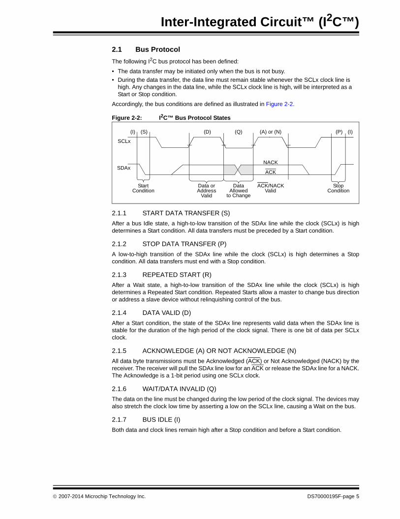
Accordingly, the bus conditions are defined as illustrated in Figure 2-2.
Figure 2-2: I2C™ Bus Protocol States
2.1.1 START DATA TRANSFER (S)
After a bus Idle state, a high-to-low transition of the SDAx line while the clock (SCLx) is highdetermines a Start condition. All data transfers must be preceded by a Start condition.
2.1.2 STOP DATA TRANSFER (P)
A low-to-high transition of the SDAx line while the clock (SCLx) is high determines a Stopcondition. All data transfers must end with a Stop condition.
2.1.3 REPEATED START (R)
After a Wait state, a high-to-low transition of the SDAx line while the clock (SCLx) is highdetermines a Repeated Start condition. Repeated Starts allow a master to change bus directionor address a slave device without relinquishing control of the bus.
2.1.4 DATA VALID (D)
After a Start condition, the state of the SDAx line represents valid data when the SDAx line isstable for the duration of the high period of the clock signal. There is one bit of data per SCLxclock.
2.1.5 ACKNOWLEDGE (A) OR NOT ACKNOWLEDGE (N)
All data byte transmissions must be Acknowledged (ACK) or Not Acknowledged (NACK) by thereceiver. The receiver will pull the SDAx line low for an ACK or release the SDAx line for a NACK.The Acknowledge is a 1-bit period using one SCLx clock.
2.1.6 WAIT/DATA INVALID (Q)
The data on the line must be changed during the low period of the clock signal. The devices mayalso stretch the clock low time by asserting a low on the SCLx line, causing a Wait on the bus.
2.1.7 BUS IDLE (I)
Both data and clock lines remain high after a Stop condition and before a Start condition.
AddressValid
DataAllowed
to Change
StopCondition
StartCondition
SCLx
SDAx
(I) (S) (D) (A) or (N) (P) (I)
Data or
(Q)
ACK/NACKValid
NACK
ACK
2007-2014 Microchip Technology Inc. DS70000195F-page 5
dsPIC33/PIC24 Family Reference Manual
2.2 Message Protocol
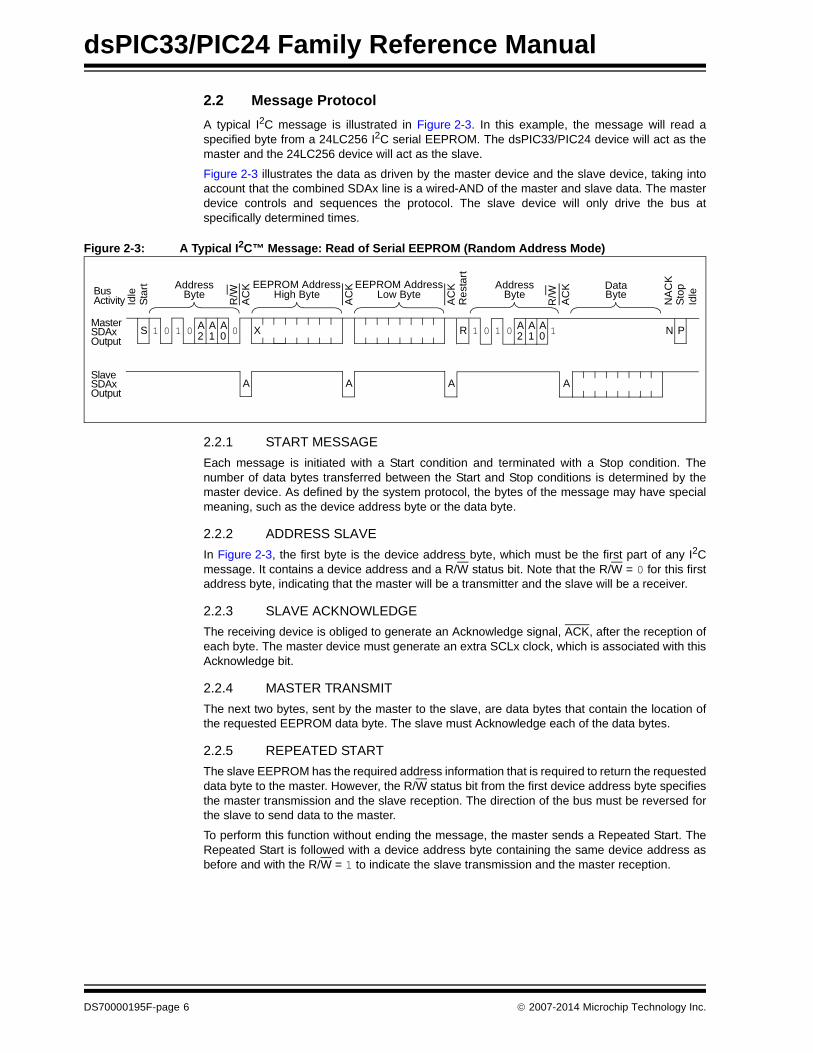
A typical I2C message is illustrated in Figure 2-3. In this example, the message will read aspecified byte from a 24LC256 I2C serial EEPROM. The dsPIC33/PIC24 device will act as themaster and the 24LC256 device will act as the slave.
Figure 2-3 illustrates the data as driven by the master device and the slave device, taking intoaccount that the combined SDAx line is a wired-AND of the master and slave data. The masterdevice controls and sequences the protocol. The slave device will only drive the bus atspecifically determined times.
Figure 2-3: A Typical I2C™ Message: Read of Serial EEPROM (Random Address Mode)
2.2.1 START MESSAGE
Each message is initiated with a Start condition and terminated with a Stop condition. Thenumber of data bytes transferred between the Start and Stop conditions is determined by themaster device. As defined by the system protocol, the bytes of the message may have specialmeaning, such as the device address byte or the data byte.
2.2.2 ADDRESS SLAVE
In Figure 2-3, the first byte is the device address byte, which must be the first part of any I2Cmessage. It contains a device address and a R/W status bit. Note that the R/W = 0 for this firstaddress byte, indicating that the master will be a transmitter and the slave will be a receiver.
2.2.3 SLAVE ACKNOWLEDGE
The receiving device is obliged to generate an Acknowledge signal, ACK, after the reception ofeach byte. The master device must generate an extra SCLx clock, which is associated with thisAcknowledge bit.
2.2.4 MASTER TRANSMIT
The next two bytes, sent by the master to the slave, are data bytes that contain the location ofthe requested EEPROM data byte. The slave must Acknowledge each of the data bytes.
2.2.5 REPEATED START
The slave EEPROM has the required address information that is required to return the requesteddata byte to the master. However, the R/W status bit from the first device address byte specifiesthe master transmission and the slave reception. The direction of the bus must be reversed forthe slave to send data to the master.
To perform this function without ending the message, the master sends a Repeated Start. TheRepeated Start is followed with a device address byte containing the same device address asbefore and with the R/W = 1 to indicate the slave transmission and the master reception.
X
Bus
MasterSDAx
Sta
rt AddressByte
EEPROM AddressHigh Byte
EEPROM AddressLow Byte
AddressByte
DataByte
S 1 0 1 0 A A A 02 1 0 R 1 0 1 0 A A A 12 1 0 P
SlaveSDAx
Activity
N
AAAA
Output
Output
Idle
R/W
AC
K
AC
K
AC
KR
est
art
AC
K
NA
CK
Sto
pId
le
R/W
DS70000195F-page 6 2007-2014 Microchip Technology Inc.
Inter-Integrated Circuit™ (I2C™)
2.2.6 SLAVE REPLY
The slave transmits the data byte by driving the SDAx line, while the master continues tooriginate clocks but releases its SDAx drive.
2.2.7 MASTER ACKNOWLEDGE
During reads, a master must terminate data requests to the slave by generating a NACK on thelast byte of the message.
2.2.8 STOP MESSAGE
The master sends a Stop signal to terminate the message and returns the bus to an Idle state.
2007-2014 Microchip Technology Inc. DS70000195F-page 7
dsPIC33/PIC24 Family Reference Manual
3.0 CONTROL AND STATUS REGISTERS
The I2C module has registers for operation that are accessible by the user application. Allregisters are accessible in either Byte or Word mode. The registers are as follows:
• I2CxCON: I2Cx Control Register or I2CxCONL: I2Cx Control Register Low and I2CxCONH: I2Cx Control Register High
These registers allow control of the module’s operation.
• I2CxSTAT: I2Cx Status Register
This register contains status flags indicating the module’s state during operation.
• I2CxMSK: I2Cx Slave Mode Address Mask Register
This register designates which bit positions in the I2CxADD register can be ignored, whichallows for multiple address support.
• ISRCCON: I2Cx Current Source Control Register(1)
This register allows control of the current source module.
• I2CxRCV: I2Cx Receive Buffer Register
This is the buffer register from which data bytes can be read. The I2CxRCV register is aread-only register.
• I2CxTRN: I2CxTransmit Register
This is the Transmit register. The bytes are written to this register during a transmitoperation. The I2CxTRN register is a read/write register.
This register holds the BRG reload value for the I2C module BRG.
The transmit data is written to the I2CxTRN register. This register is used when the moduleoperates as a master transmitting data to the slave or when it operates as a slave sending replydata to the master. As the message progresses, the I2CxTRN register shifts out the individualbits. Therefore, the I2CxTRN register cannot be written to unless the bus is Idle.
The data being received by either the master or the slave is shifted into a non-accessible shiftregister, I2CxRSR. When a complete byte is received, the byte transfers to the I2CxRCV register.In receive operations, the I2CxRSR and I2CxRCV registers create a double-buffered receiver.This allows reception of the next byte to begin before reading the current byte of the receiveddata.
If the module receives another complete byte before the user software reads the previous bytefrom the I2CxRCV register, a receiver overflow occurs and sets the I2COV bit (I2CxSTAT<6>).The byte in the I2CxRSR register is lost if (BOEN = 0). Further reception and clock stretchingare disabled until the I2C module sees a Start/Repeated, Start/Stop condition on the bus. If theI2COV flag has been cleared, the reception can proceed normally. If the I2COV flag is notcleared, the module will receive the next byte correctly, but will send a NACK. It will then beunable to receive further bytes or stretch the clock until it detects a Start/Repeated and Start/Stopcondition.
The I2CxADD register holds the slave device address. In 10-Bit Addressing mode, all bits arerelevant. In 7-Bit Addressing mode, only the I2CxADD<6:0> bits are relevant. TheI2CxADD<6:0> bits correspond to the upper 7 bits in the address byte. The read/write bit is notincluded in the value in this register. The A10M bit (I2CxCON<10> or I2CxCONL<10>) specifiesthe expected mode of the slave address. By using the I2CxMSK register with the I2CxADD reg-ister in Slave Addressing mode, one or more bit positions can be removed from the exactaddress matching, allowing the module, in Slave mode, to respond to multiple addresses.
Note 1: The I2CxCONL, I2CxCONH and ISRCCON registers are not available on alldevices. Refer to the specific device data sheet for availability.
DS70000195F-page 8 2007-2014 Microchip Technology Inc.
Inter-Integrated Circuit™ (I2C™)
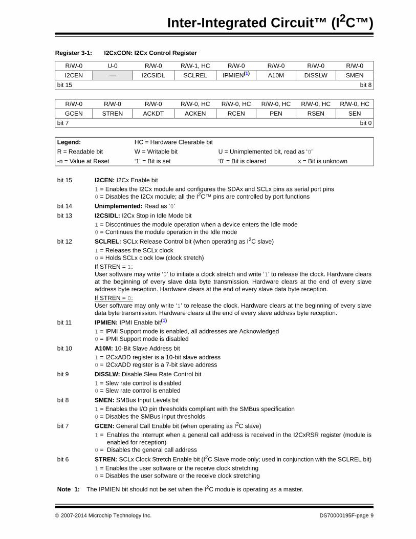
Register 3-1: I2CxCON: I2Cx Control Register
R/W-0 U-0 R/W-0 R/W-1, HC R/W-0 R/W-0 R/W-0 R/W-0
I2CEN — I2CSIDL SCLREL IPMIEN(1) A10M DISSLW SMEN
bit 15 bit 8
R/W-0 R/W-0 R/W-0 R/W-0, HC R/W-0, HC R/W-0, HC R/W-0, HC R/W-0, HC
GCEN STREN ACKDT ACKEN RCEN PEN RSEN SEN
bit 7 bit 0
Legend: HC = Hardware Clearable bit
R = Readable bit W = Writable bit U = Unimplemented bit, read as ‘0’
-n = Value at Reset ‘1’ = Bit is set ‘0’ = Bit is cleared x = Bit is unknown
bit 15 I2CEN: I2Cx Enable bit
1 = Enables the I2Cx module and configures the SDAx and SCLx pins as serial port pins0 = Disables the I2Cx module; all the I2C™ pins are controlled by port functions
bit 14 Unimplemented: Read as ‘0’
bit 13 I2CSIDL: I2Cx Stop in Idle Mode bit
1 = Discontinues the module operation when a device enters the Idle mode0 = Continues the module operation in the Idle mode
bit 12 SCLREL: SCLx Release Control bit (when operating as I2C slave)
If STREN = 1:User software may write ‘0’ to initiate a clock stretch and write ‘1’ to release the clock. Hardware clearsat the beginning of every slave data byte transmission. Hardware clears at the end of every slaveaddress byte reception. Hardware clears at the end of every slave data byte reception.
If STREN = 0:User software may only write ‘1’ to release the clock. Hardware clears at the beginning of every slavedata byte transmission. Hardware clears at the end of every slave address byte reception.
bit 11 IPMIEN: IPMI Enable bit(1)
1 = IPMI Support mode is enabled, all addresses are Acknowledged0 = IPMI Support mode is disabled
bit 10 A10M: 10-Bit Slave Address bit
1 = I2CxADD register is a 10-bit slave address0 = I2CxADD register is a 7-bit slave address
bit 9 DISSLW: Disable Slew Rate Control bit
1 = Slew rate control is disabled0 = Slew rate control is enabled
bit 8 SMEN: SMBus Input Levels bit
1 = Enables the I/O pin thresholds compliant with the SMBus specification0 = Disables the SMBus input thresholds
bit 7 GCEN: General Call Enable bit (when operating as I2C slave)
1 = Enables the interrupt when a general call address is received in the I2CxRSR register (module isenabled for reception)
0 = Disables the general call address
bit 6 STREN: SCLx Clock Stretch Enable bit (I2C Slave mode only; used in conjunction with the SCLREL bit)
1 = Enables the user software or the receive clock stretching0 = Disables the user software or the receive clock stretching
Note 1: The IPMIEN bit should not be set when the I2C module is operating as a master.
2007-2014 Microchip Technology Inc. DS70000195F-page 9
dsPIC33/PIC24 Family Reference Manual
bit 5 ACKDT: Acknowledge Data bit (I2C Master mode; receive operation only)Value that will be transmitted when the user software initiates an Acknowledge sequence.
1 = Sends a NACK during an Acknowledge0 = Sends an ACK during an Acknowledge
bit 4 ACKEN: Acknowledge Sequence Enable bit (I2C Master mode receive operation)
1 = Initiates the Acknowledge sequence on the SDAx and SCLx pins and transmits the ACKDT data bit(hardware clears at the end of the master Acknowledge sequence)
0 = Acknowledge sequence is not in progress
bit 3 RCEN: Receive Enable bit (I2C Master mode)
1 = Enables Receive mode for I2C (hardware clears at the end of eighth bit of master receive data byte)0 = Receive sequence is not in progress
bit 2 PEN: Stop Condition Enable bit (I2C Master mode)
1 = Initiates the Stop condition on the SDAx and SCLx pins (hardware clears at the end of master Stopsequence)
0 = Stop condition is not in progress
bit 1 RSEN: Repeated Start Condition Enable bit (I2C Master mode)
1 = Initiates the Repeated Start condition on the SDAx and SCLx pins (hardware clears at the end ofmaster Repeated Start sequence)
0 = Repeated Start condition is not in progress
bit 0 SEN: Start Condition Enable bit (I2C Master mode)
1 = Initiates the Start condition on the SDAx and SCLx pins (hardware clears at the end of master Startsequence)
0 = Start condition is not in progress
Register 3-1: I2CxCON: I2Cx Control Register (Continued)
Note 1: The IPMIEN bit should not be set when the I2C module is operating as a master.
DS70000195F-page 10 2007-2014 Microchip Technology Inc.
Inter-Integrated Circuit™ (I2C™)
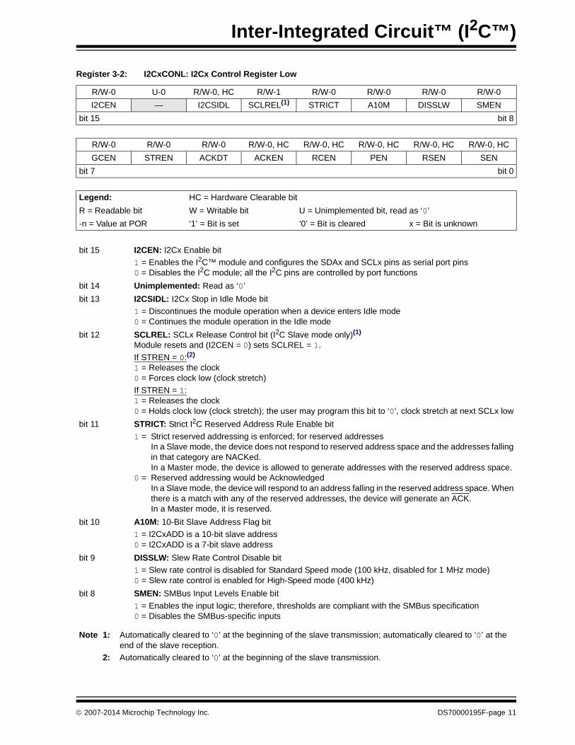
Register 3-2: I2CxCONL: I2Cx Control Register Low
R/W-0 U-0 R/W-0, HC R/W-1 R/W-0 R/W-0 R/W-0 R/W-0
I2CEN — I2CSIDL SCLREL(1) STRICT A10M DISSLW SMEN
bit 15 bit 8
R/W-0 R/W-0 R/W-0 R/W-0, HC R/W-0, HC R/W-0, HC R/W-0, HC R/W-0, HC
GCEN STREN ACKDT ACKEN RCEN PEN RSEN SEN
bit 7 bit 0
Legend: HC = Hardware Clearable bit
R = Readable bit W = Writable bit U = Unimplemented bit, read as ‘0’
-n = Value at POR ‘1’ = Bit is set ‘0’ = Bit is cleared x = Bit is unknown
bit 15 I2CEN: I2Cx Enable bit
1 = Enables the I2C™ module and configures the SDAx and SCLx pins as serial port pins0 = Disables the I2C module; all the I2C pins are controlled by port functions
bit 14 Unimplemented: Read as ‘0’
bit 13 I2CSIDL: I2Cx Stop in Idle Mode bit
1 = Discontinues the module operation when a device enters Idle mode0 = Continues the module operation in the Idle mode
bit 12 SCLREL: SCLx Release Control bit (I2C Slave mode only)(1)
If STREN = 1:1 = Releases the clock0 = Holds clock low (clock stretch); the user may program this bit to ‘0’, clock stretch at next SCLx low
bit 11 STRICT: Strict I2C Reserved Address Rule Enable bit
1 = Strict reserved addressing is enforced; for reserved addressesIn a Slave mode, the device does not respond to reserved address space and the addresses fallingin that category are NACKed.In a Master mode, the device is allowed to generate addresses with the reserved address space.
0 = Reserved addressing would be AcknowledgedIn a Slave mode, the device will respond to an address falling in the reserved address space. Whenthere is a match with any of the reserved addresses, the device will generate an ACK.In a Master mode, it is reserved.
bit 10 A10M: 10-Bit Slave Address Flag bit
1 = I2CxADD is a 10-bit slave address0 = I2CxADD is a 7-bit slave address
bit 9 DISSLW: Slew Rate Control Disable bit
1 = Slew rate control is disabled for Standard Speed mode (100 kHz, disabled for 1 MHz mode)0 = Slew rate control is enabled for High-Speed mode (400 kHz)
bit 8 SMEN: SMBus Input Levels Enable bit
1 = Enables the input logic; therefore, thresholds are compliant with the SMBus specification0 = Disables the SMBus-specific inputs
Note 1: Automatically cleared to ‘0’ at the beginning of the slave transmission; automatically cleared to ‘0’ at the end of the slave reception.
2: Automatically cleared to ‘0’ at the beginning of the slave transmission.
2007-2014 Microchip Technology Inc. DS70000195F-page 11
dsPIC33/PIC24 Family Reference Manual
bit 7 GCEN: General Call Enable bit (I2C Slave mode only)
1 = Enables the interrupt when a general call address is received in I2CxRSR; the module is enabled forreception
0 = General call address is disabled
bit 6 STREN: SCLx Clock Stretch Enable bitIn I2C Slave mode only; used in conjunction with the SCLREL bit.
In I2C Master mode during Master Receive mode. The value that will be transmitted when the userinitiates an Acknowledge sequence at the end of a receive.
In I2C Slave mode when AHEN = 1 or DHEN = 1. The value that the slave will transmit when it initiatesan Acknowledge sequence at the end of an address or data reception.
1 = NACK is sent0 = ACK is sent
bit 4 ACKEN: Acknowledge Sequence Enable bitIn I2C Master mode only; applicable during Master Receive mode.
1 = Initiates the Acknowledge sequence on the SDAx and SCLx pins, and transmits the ACKDT data bit0 = Acknowledge sequence is in Idle mode
bit 3 RCEN: Receive Enable bit (I2C Master mode only)
1 = Enables Receive mode for I2C; automatically cleared by hardware at the end of an 8-bit receivedata byte
0 = Receive sequence is not in progress
bit 2 PEN: Stop Condition Enable bit (I2C Master mode only)
1 = Initiates the Stop condition on the SDAx and SCLx pins0 = Stop condition is in Idle mode
bit 1 RSEN: Restart Condition Enable bit (I2C Master mode only)
1 = Initiates the Restart condition on the SDAx and SCLx pins0 = Restart condition is in Idle mode
bit 0 SEN: Start Condition Enable bit (I2C Master mode only)
1 = Initiates the Start condition on the SDAx and SCLx pins0 = Start condition is in Idle mode
Register 3-2: I2CxCONL: I2Cx Control Register Low (Continued)
Note 1: Automatically cleared to ‘0’ at the beginning of the slave transmission; automatically cleared to ‘0’ at the end of the slave reception.
2: Automatically cleared to ‘0’ at the beginning of the slave transmission.
DS70000195F-page 12 2007-2014 Microchip Technology Inc.
Inter-Integrated Circuit™ (I2C™)
Register 3-3: I2CxCONH: I2Cx Control Register High
U-0 U-0 U-0 U-0 U-0 U-0 U-0 U-0
— — — — — — — —
bit 15 bit 8
U-0 R/W-0 R/W-0 R/W-0 R/W-0 R/W-0 R/W-0 R/W-0
— PCIE SCIE BOEN SDAHT SBCDE AHEN DHEN
bit 7 bit 0
Legend:
R = Readable bit W = Writable bit U = Unimplemented bit, read as ‘0’
-n = Value at POR ‘1’ = Bit is set ‘0’ = Bit is cleared x = Bit is unknown
bit 15-7 Unimplemented: Read as ‘0’
bit 6 PCIE: Stop Condition Interrupt Enable bit (I2C™ Slave mode only)
1 = Enables the interrupt on detection of a Stop condition0 = Stop detection interrupts are disabled
bit 5 SCIE: Start Condition Interrupt Enable bit (I2C Slave mode only)
1 = Enables the interrupt on detection of a Start or Restart condition0 = Start detection interrupts are disabled
bit 4 BOEN: Buffer Overwrite Enable bit (I2C Slave mode only)
1 = The I2CxRCV register is updated and an ACK is generated for a received address or data byte,ignoring the state of the I2COV bit only if the RBF bit = 0
0 = The I2CxRCV register is only updated when the I2COV bit is clear
bit 3 SDAHT: SDAx Hold Time Selection bit
1 = Minimum of 300 ns hold time on SDAx after the falling edge of the SCLx clock0 = Minimum of 100 ns hold time on SDAx after the falling edge the of SCLx clock
bit 2 SBCDE: Slave Mode Bus Collision Detect Enable bit (I2C Slave mode only)If, on the rising edge of the SCLx, SDAx is sampled low when the module is outputting a high state, theBCL bit is set and the bus goes into Idle mode. This Detection mode is valid only during the data andACK transmit sequences.
1 = Enables the slave bus collision interrupts0 = Disables the slave bus collision interrupts
bit 1 AHEN: Address Hold Enable bit (I2C Slave mode only)
1 = Following the falling edge of the eighth SCLx clock for a matching received address byte; theSCLREL bit (I2CxCONL<12>) will be cleared and the SCLx will be held low
0 = Address holding is disabled
bit 0 DHEN: Data Hold Enable bit (I2C Slave mode only)
1 = Following the eighth falling edge of the SCLx clock for a received data byte; slave hardware clearsthe SCLREL bit (I2CxCONL<12>) and SCLx is held low
0 = Data holding is disabled
2007-2014 Microchip Technology Inc. DS70000195F-page 13
Legend: C = Clearable bit HSC = Hardware Settable/Clearable bit
R = Readable bit W = Writable bit U = Unimplemented bit, read as ‘0’
-n = Value at POR ‘1’ = Bit is set ‘0’ = Bit is cleared x = Bit is unknown
HS = Hardware Settable bit
bit 15 ACKSTAT: Acknowledge Status bit
1 = NACK received from slave0 = ACK received from slaveHardware sets or clears at the end of slave or master Acknowledge.
bit 14 TRSTAT: Transmit Status bit (I2C™ Master mode transmit operation)
1 = Master transmit is in progress (8 bits + ACK)0 = Master transmit is not in progressHardware sets at the beginning of master transmission; hardware clears at the end of slave Acknowledge.
bit 13 ACKTIM: Acknowledge Time Status bit (valid in I2C Slave mode only)(1)
1 = Indicates that the I2C bus is in an Acknowledge sequence; set on the falling edge of eighth SCLx clock0 = Not an Acknowledge sequence, cleared on ninth rising edge of the SCLx clockHardware sets at the beginning of master transmission; hardware clears at the end of slave Acknowledge.
bit 12-11 Unimplemented: Read as ‘0’
bit 10 BCL: Bus Collision Detect bit (Master and Slave modes)
1 = A bus collision has been detected during a master or slave operation0 = No collisionHardware sets at detection of a bus collision; clears when I2C module is disabled, I2CEN = 0.
bit 9 GCSTAT: General Call Status bit
1 = General call address was received0 = General call address was not receivedHardware sets when address matches general call address; hardware clears at Stop detection.
bit 8 ADD10: 10-Bit Address Status bit
1 = 10-bit address was matched0 = 10-bit address was not matchedHardware sets at match of second byte of matched 10-bit address; hardware clears at Stop detection.
bit 7 IWCOL: I2Cx Write Collision Detect bit
1 = An attempt to write to the I2CxTRN register failed because the I2C module is busy0 = No collisionHardware sets at occurrence of a write to the I2CxTRN register while busy (cleared by software).
bit 6 I2COV: I2Cx Receive Overflow Flag bit
1 = A byte is received while the I2CxRCV register is still holding the previous byte0 = No overflowHardware sets at attempt to transfer the I2CxRSR register to the I2CxRCV register (cleared by software).
Note 1: Refer to the specific device data sheet for availability of the ACKTIM bit.
DS70000195F-page 14 2007-2014 Microchip Technology Inc.
Inter-Integrated Circuit™ (I2C™)
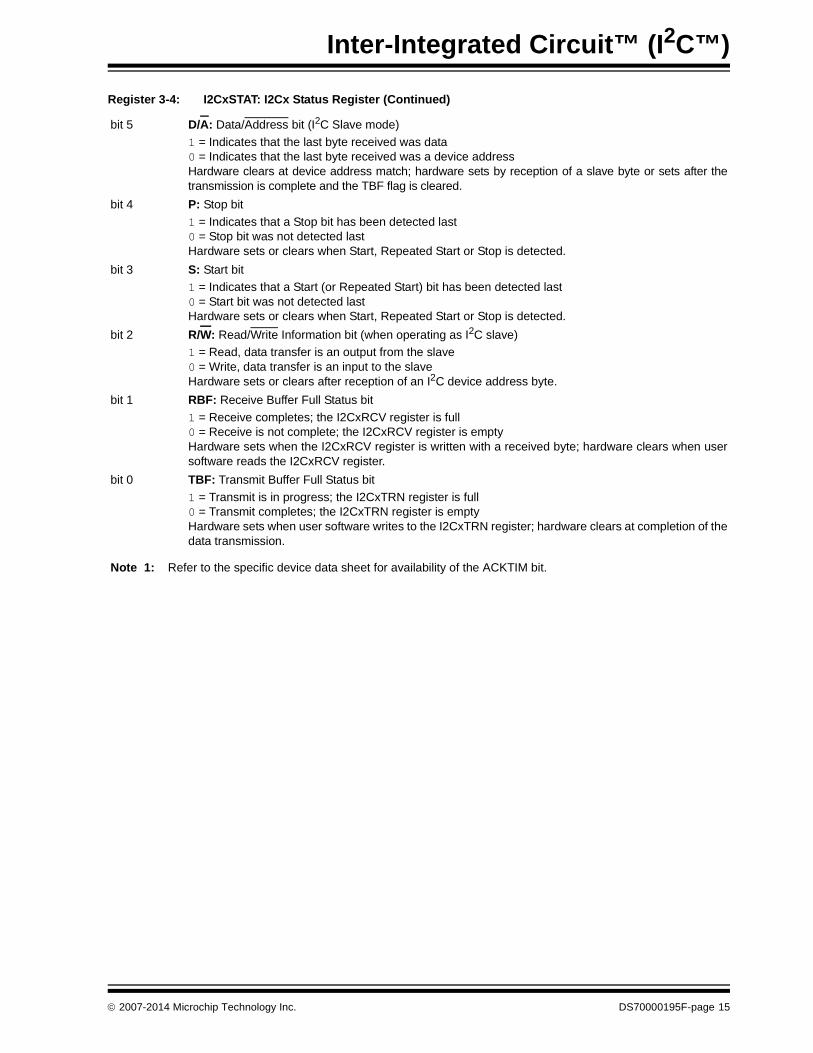
bit 5 D/A: Data/Address bit (I2C Slave mode)
1 = Indicates that the last byte received was data0 = Indicates that the last byte received was a device addressHardware clears at device address match; hardware sets by reception of a slave byte or sets after thetransmission is complete and the TBF flag is cleared.
bit 4 P: Stop bit
1 = Indicates that a Stop bit has been detected last0 = Stop bit was not detected lastHardware sets or clears when Start, Repeated Start or Stop is detected.
bit 3 S: Start bit
1 = Indicates that a Start (or Repeated Start) bit has been detected last0 = Start bit was not detected lastHardware sets or clears when Start, Repeated Start or Stop is detected.
bit 2 R/W: Read/Write Information bit (when operating as I2C slave)
1 = Read, data transfer is an output from the slave0 = Write, data transfer is an input to the slaveHardware sets or clears after reception of an I2C device address byte.
bit 1 RBF: Receive Buffer Full Status bit
1 = Receive completes; the I2CxRCV register is full0 = Receive is not complete; the I2CxRCV register is emptyHardware sets when the I2CxRCV register is written with a received byte; hardware clears when usersoftware reads the I2CxRCV register.
bit 0 TBF: Transmit Buffer Full Status bit
1 = Transmit is in progress; the I2CxTRN register is full0 = Transmit completes; the I2CxTRN register is emptyHardware sets when user software writes to the I2CxTRN register; hardware clears at completion of thedata transmission.
Register 3-4: I2CxSTAT: I2Cx Status Register (Continued)
Note 1: Refer to the specific device data sheet for availability of the ACKTIM bit.
2007-2014 Microchip Technology Inc. DS70000195F-page 15
R = Readable bit W = Writable bit U = Unimplemented bit, read as ‘0’
-n = Value at Reset ‘1’ = Bit is set ‘0’ = Bit is cleared x = Bit is unknown
bit 15-10 Unimplemented: Read as ‘0’
bit 9-0 AMSK<9:0>: Mask for Address Bit x Select bits
For 10-Bit Address:1 = Enables masking for bit Ax of the incoming message address; bit match is not required in this position0 = Disables masking for bit Ax; bit match is required in this position
For 7-Bit Address (I2CxMSK<6:0> only):1 = Enables masking for bit Ax + 1 of the incoming message address; bit match is not required in this position0 = Disables masking for bit Ax + 1; bit match is required in this position
DS70000195F-page 16 2007-2014 Microchip Technology Inc.
Inter-Integrated Circuit™ (I2C™)
Register 3-6: ISRCCON: I2Cx Current Source Control Register(1)
R = Readable bit W = Writable bit U = Unimplemented bit, read as ‘0’
-n = Value at POR ‘1’ = Bit is set ‘0’ = Bit is cleared x = Bit is unknown
bit 15 ISRCEN: I2Cx Current Source Enable bit
1 = Current source is enabled0 = Current source is disabled
bit 14-11 Unimplemented: Read as ‘0’
bit 10-8 OUTSEL<2:0>: Output Select for Current bits
111 = Reserved110 = Reserved101 = Reserved100 = Selected input pin is ISRC4 (AN4)011 = Selected input pin is ISRC3 (AN5)010 = Selected input pin is ISRC2 (AN6)001 = Selected input pin is ISRC1 (AN7)000 = No output is selected
bit 7-6 Unimplemented: Read as ‘0’
bit 5-0 ISRCCAL<5:0>: I2Cx Current Source Calibration bits(2)
Note 1: This register is not available on all devices. Refer to the specific device data sheet for availability.
2: The calibration value must be retrieved from the Flash memory and stored in this location at start-up time.
2007-2014 Microchip Technology Inc. DS70000195F-page 17
dsPIC33/PIC24 Family Reference Manual
4.0 ENABLING I2C OPERATION
The I2C module is enabled by setting the I2CEN bit (I2CxCON<15> or I2CxCONL<15>). The I2Cmodule fully implements all master and slave functions. When the module is enabled, the masterand slave functions are active simultaneously and will respond according to the user software orbus events.
When initially enabled, the module will release the SDAx and SCLx pins, putting the bus into anIdle state. The master functions will remain in an Idle state unless the user software sets the SENcontrol bit and the data is loaded into the I2CxTRN register. These two actions initiate a masterevent.
When the master logic is active, the slave logic also remains active. Therefore, the slavefunctions will begin to monitor the bus. If the slave logic detects a Start event and a valid addresson the bus, the slave logic will begin a slave transaction.
4.1 I2C I/O Pins
Two pins are used for the bus operation. These are the SCLx pin, which is the clock, and theSDAx pin, which is the data. When the module is enabled, assuming no other module with higherpriority has control, the module will assume control of the SDAx and SCLx pins. The usersoftware need not be concerned with the state of the port I/O of the pins, as the module overridesthe port state and direction. At initialization, the pins are tri-stated (released).
4.2 I2C Interrupts
The I2C module generates three interrupts: MI2CxIF, SI2CxIF and I2CxBCIF. The MI2CxIFinterrupt is assigned to the master events, the SI2CxIF interrupt is assigned to the slave eventsand the I2CxBCIF is assigned for the bus collision interrupt. These interrupts set a correspondinginterrupt flag bit and interrupt the user software process if the corresponding interrupt enable bitis set, and the corresponding interrupt priority is higher than the CPU interrupt priority.
The MI2CxIF interrupt is generated on completion of the following master message events:
• Start condition
• Stop condition
• Data transfer byte transmitted or received
• Acknowledge transmit
• Repeated Start
• Detection of a bus collision event.
The SI2CxIF interrupt is generated on detection of a message directed to the slave, including thefollowing events:
• Detection of a Start condition (see Note 1)
• Detection of a Stop condition (see Note 1)
• Detection of a Repeated Start condition (see Note 1)
• Detection of a valid device address (including general call) during receiving data
• Request to transmit the data (ACK) or to stop the data transmission (NACK)
• Reception of data
The I2CxBCIF interrupt is generated on a bus collision event in master/slave transmit operation:
• Start condition (master)
• Stop condition (master)
• Repeated Start (master)
• Data (master and slave)
• Acknowledge transmit (master and slave)
Note: In some devices, the bus collision interrupt is not tied with the MI2CxIF interrupt.
Note 1: These interrupts may not be present on all devices. Refer to the specific devicedata sheet for availability.
DS70000195F-page 18 2007-2014 Microchip Technology Inc.
Inter-Integrated Circuit™ (I2C™)
4.3 Setting Baud Rate When Operating as a Bus Master
When operating as an I2C master, the module must generate the system SCLx clock. Generally,the I2C system clocks are specified to be either 100 kHz, 400 kHz or 1 MHz. The system clockrate is specified as the minimum SCLx low time, plus the minimum SCLx high time. In mostcases, that is defined by two BRG periods (TBRG).
The reload value for the BRG is the I2CxBRG register, as illustrated in Figure 4-1. When the BRGis loaded with this value, the generator counts down to zero and stops until another reload hastaken place. The BRG is reloaded automatically on baud rate restart. For example, if clocksynchronization is taking place, the BRG will be reloaded when the SCLx pin is sampled high.
Equation 4-1 shows the formula for computing the BRG reload value.
Equation 4-1: BRG Reload Value Calculation
Figure 4-1: Baud Rate Generator Block Diagram
Note: The I2CxBRG register values that are less than two are not supported.
Note: Equation 4-1 is only for a design guideline. Due to system-dependent parameters,the actual baud rate may differ slightly. Testing is required to confirm that the actualbaud rate meets the system requirements. Otherwise, the value of the I2CxBRGregister has to be adjusted.
Typical value of delay varies from 110 ns to 130 ns.
Note 1: Refer to the specific device data sheet for BRG reload value calculation.
2: If there is no calculation mentioned in the data sheet, then the default BRG reload value calculation should be considered.
or
Down Counter TBRG = TCY or TCY/2(1)
I2CxBRG<8:0>
SCLx ReloadControl
Reload
Note 1: Refer to specific device data sheet for the clock rate.
2TSCL
2007-2014 Microchip Technology Inc. DS70000195F-page 19
dsPIC33/PIC24 Family Reference Manual
5.0 COMMUNICATING AS A MASTER IN A SINGLE MASTER ENVIRONMENT
The I2C module’s typical operation in a system is using the I2C to communicate with an I2Cperipheral, such as an I2C serial memory. In an I2C system, the master controls the sequence ofall data communication on the bus. In this example, the dsPIC33/PIC24 device and its I2Cmodule have the role of the single master in the system. As the single master, it is responsiblefor generating the SCLx clock and controlling the message protocol.
The I2C module controls individual portions of the I2C message protocol; however, sequencingof the components of the protocol to construct a complete message is performed by the usersoftware.
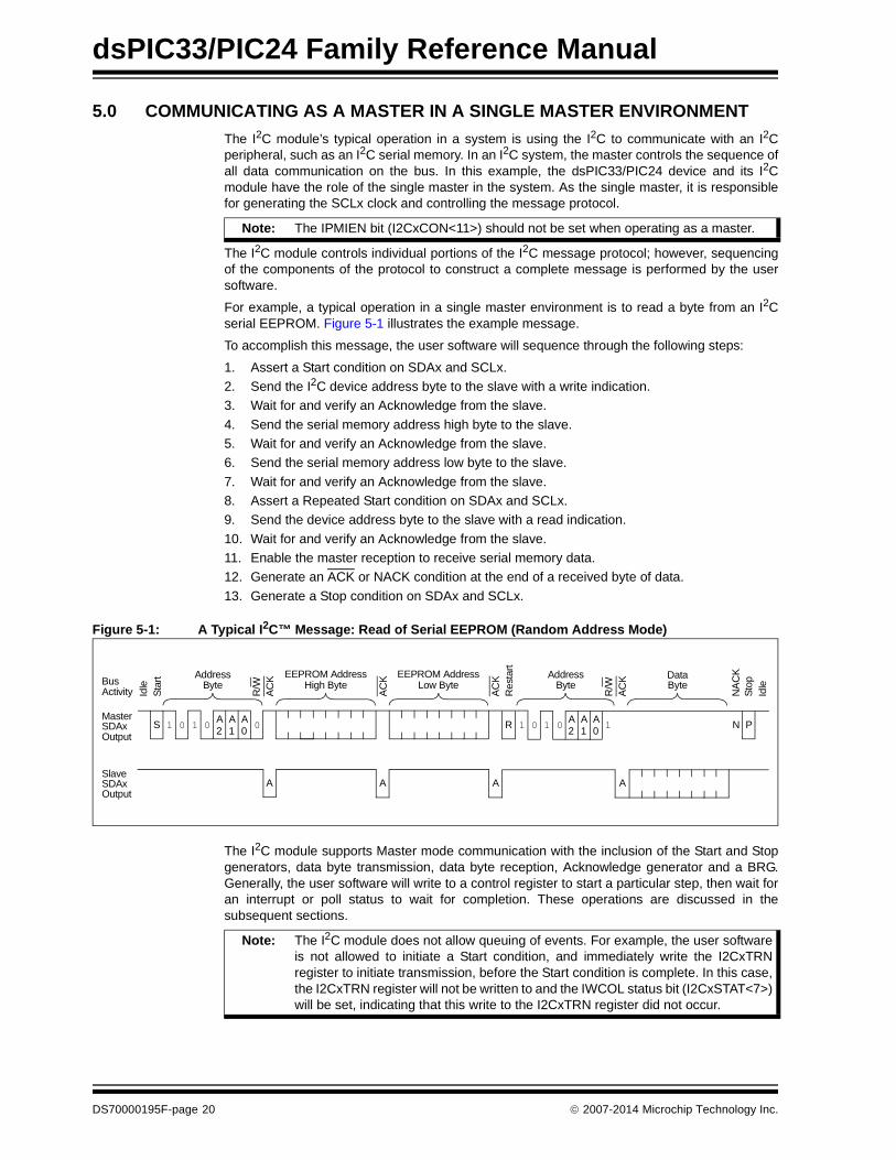
For example, a typical operation in a single master environment is to read a byte from an I2Cserial EEPROM. Figure 5-1 illustrates the example message.
To accomplish this message, the user software will sequence through the following steps:
1. Assert a Start condition on SDAx and SCLx.
2. Send the I2C device address byte to the slave with a write indication.
3. Wait for and verify an Acknowledge from the slave.
4. Send the serial memory address high byte to the slave.
5. Wait for and verify an Acknowledge from the slave.
6. Send the serial memory address low byte to the slave.
7. Wait for and verify an Acknowledge from the slave.
8. Assert a Repeated Start condition on SDAx and SCLx.
9. Send the device address byte to the slave with a read indication.
10. Wait for and verify an Acknowledge from the slave.
11. Enable the master reception to receive serial memory data.
12. Generate an ACK or NACK condition at the end of a received byte of data.
13. Generate a Stop condition on SDAx and SCLx.
Figure 5-1: A Typical I2C™ Message: Read of Serial EEPROM (Random Address Mode)
The I2C module supports Master mode communication with the inclusion of the Start and Stopgenerators, data byte transmission, data byte reception, Acknowledge generator and a BRG.Generally, the user software will write to a control register to start a particular step, then wait foran interrupt or poll status to wait for completion. These operations are discussed in thesubsequent sections.
Note: The IPMIEN bit (I2CxCON<11>) should not be set when operating as a master.
Bus
MasterSDAx
Sta
rt AddressByte
EEPROM AddressHigh Byte
EEPROM AddressLow Byte
AddressByte
DataByte
S 1 0 1 0 A A A 02 1 0
R 1 0 1 0 A A A 12 1 0
P
SlaveSDAx
Activity
N
AAAA
Output
Output
Idle
R/W
AC
K
AC
K
AC
KR
esta
rt
R/W
AC
K
NA
CK
Sto
pId
le
Note: The I2C module does not allow queuing of events. For example, the user softwareis not allowed to initiate a Start condition, and immediately write the I2CxTRNregister to initiate transmission, before the Start condition is complete. In this case,the I2CxTRN register will not be written to and the IWCOL status bit (I2CxSTAT<7>)will be set, indicating that this write to the I2CxTRN register did not occur.
DS70000195F-page 20 2007-2014 Microchip Technology Inc.
Inter-Integrated Circuit™ (I2C™)
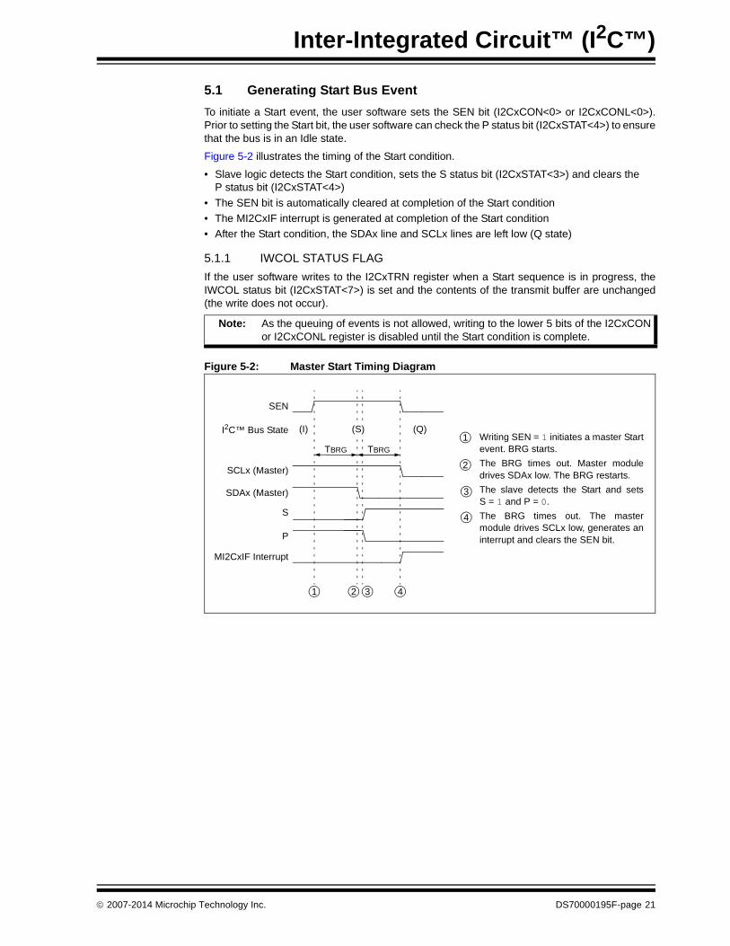
5.1 Generating Start Bus Event
To initiate a Start event, the user software sets the SEN bit (I2CxCON<0> or I2CxCONL<0>).Prior to setting the Start bit, the user software can check the P status bit (I2CxSTAT<4>) to ensurethat the bus is in an Idle state.
Figure 5-2 illustrates the timing of the Start condition.
• Slave logic detects the Start condition, sets the S status bit (I2CxSTAT<3>) and clears the P status bit (I2CxSTAT<4>)
• The SEN bit is automatically cleared at completion of the Start condition
• The MI2CxIF interrupt is generated at completion of the Start condition
• After the Start condition, the SDAx line and SCLx lines are left low (Q state)
5.1.1 IWCOL STATUS FLAG
If the user software writes to the I2CxTRN register when a Start sequence is in progress, theIWCOL status bit (I2CxSTAT<7>) is set and the contents of the transmit buffer are unchanged(the write does not occur).
Figure 5-2: Master Start Timing Diagram
Note: As the queuing of events is not allowed, writing to the lower 5 bits of the I2CxCONor I2CxCONL register is disabled until the Start condition is complete.
SCLx (Master)
SDAx (Master)
S
SEN
MI2CxIF Interrupt
TBRG
1 2 3 4
1TBRG
2
3
4
I2C™ Bus State (I) (Q)
P
(S)Writing SEN = 1 initiates a master Startevent. BRG starts.
The BRG times out. Master moduledrives SDAx low. The BRG restarts.
The slave detects the Start and setsS = 1 and P = 0.
The BRG times out. The mastermodule drives SCLx low, generates aninterrupt and clears the SEN bit.
2007-2014 Microchip Technology Inc. DS70000195F-page 21
dsPIC33/PIC24 Family Reference Manual
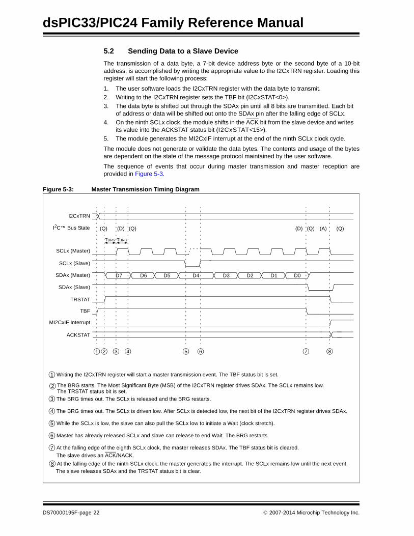
5.2 Sending Data to a Slave Device
The transmission of a data byte, a 7-bit device address byte or the second byte of a 10-bitaddress, is accomplished by writing the appropriate value to the I2CxTRN register. Loading thisregister will start the following process:
1. The user software loads the I2CxTRN register with the data byte to transmit.
2. Writing to the I2CxTRN register sets the TBF bit (I2CxSTAT<0>).
3. The data byte is shifted out through the SDAx pin until all 8 bits are transmitted. Each bitof address or data will be shifted out onto the SDAx pin after the falling edge of SCLx.
4. On the ninth SCLx clock, the module shifts in the ACK bit from the slave device and writesits value into the ACKSTAT status bit (I2CxSTAT<15>).
5. The module generates the MI2CxIF interrupt at the end of the ninth SCLx clock cycle.
The module does not generate or validate the data bytes. The contents and usage of the bytesare dependent on the state of the message protocol maintained by the user software.
The sequence of events that occur during master transmission and master reception areprovided in Figure 5-3.
Figure 5-3: Master Transmission Timing Diagram
D7 D6 D5 D4 D3 D2 D1 D0
SCLx (Master)
SCLx (Slave)
SDAx (Master)
SDAx (Slave)
TBF
I2CxTRN
MI2CxIF Interrupt
TBRG TBRG
5 6 7 81 2 3 4
Writing the I2CxTRN register will start a master transmission event. The TBF status bit is set.1
The BRG starts. The Most Significant Byte (MSB) of the I2CxTRN register drives SDAx. The SCLx remains low. 2
The BRG times out. The SCLx is released and the BRG restarts.3
The BRG times out. The SCLx is driven low. After SCLx is detected low, the next bit of the I2CxTRN register drives SDAx.4
While the SCLx is low, the slave can also pull the SCLx low to initiate a Wait (clock stretch).5
Master has already released SCLx and slave can release to end Wait. The BRG restarts.6
At the falling edge of the eighth SCLx clock, the master releases SDAx. The TBF status bit is cleared. 7
At the falling edge of the ninth SCLx clock, the master generates the interrupt. The SCLx remains low until the next event. 8The slave releases SDAx and the TRSTAT status bit is clear.
I2C™ Bus State (Q) (D) (Q) (A) (Q)(D) (Q)
TRSTAT
ACKSTAT
The TRSTAT status bit is set.
The slave drives an ACK/NACK.
DS70000195F-page 22 2007-2014 Microchip Technology Inc.
Inter-Integrated Circuit™ (I2C™)
5.2.1 SENDING A 7-BIT ADDRESS TO THE SLAVE
Sending a 7-bit device address involves sending one byte to the slave. A 7-bit address byte mustcontain the 7 bits of the I2C device address and a R/W status bit that defines whether themessage will be a write to the slave (master transmission and slave reception) or a read from theslave (slave transmission and master reception).
5.2.2 STRICT SUPPORT IN MASTER MODE
The master device is allowed to generate an address that falls in the reserved address space ifthe STRICT (I2CxCONL<11>) bit is set. For more information on the reserved address, refer toTable 7-2.
5.2.3 SENDING A 10-BIT ADDRESS TO THE SLAVE
Sending a 10-bit device address involves sending two bytes to the slave. The first byte contains 5 bitsof the I2C device address reserved for 10-Bit Addressing modes and 2 bits of the 10-bit address. Asthe next byte, which contains the remaining 8 bits of the 10-bit address, must be received by the slave,the R/W status bit in the first byte must be ‘0’, indicating master transmission and slave reception. Ifthe message data is also directed toward the slave, the master can continue sending data. However,if the master expects a reply from the slave, a Repeated Start sequence with the R/W status bit at ‘1’will change the R/W state of the message to a read of the slave.
5.2.4 RECEIVING ACKNOWLEDGE FROM THE SLAVE
On the falling edge of the eighth SCLx clock, the TBF status bit is cleared and the master willdeassert the SDAx pin, allowing the slave to respond with an Acknowledge. The master will thengenerate a ninth SCLx clock.
This allows the slave device being addressed to respond with an ACK bit during the ninth bit timeif an address match occurs or data was received properly. A slave sends an Acknowledge whenit has recognized its device address (including a general call) or when the slave has properlyreceived its data.
The status of ACK is written into the ACKSTAT bit (I2CxSTAT<15>) on the falling edge of theninth SCLx clock. After the ninth SCLx clock, the module generates the MI2CxIF interrupt andenters into the Idle state until the next data byte is loaded into the I2CxTRN register.
5.2.5 ACKSTAT STATUS FLAG
The ACKSTAT bit (I2CxSTAT<15>) is cleared when the slave has sent an Acknowledge(ACK = 0) and is set when the slave does not Acknowledge (ACK = 1).
5.2.6 TBF STATUS FLAG
When transmitting, the TBF status bit (I2CxSTAT<0>) is set when the CPU writes to the I2CxTRNregister and is cleared when all 8 bits are shifted out.
5.2.7 IWCOL STATUS FLAG
If the user software attempts to write to the I2CxTRN register when a transmit is already inprogress (that is, the module is still shifting a data byte), the IWCOL status bit (I2CxSTAT<7>) isset and the contents of the buffer are unchanged (the write does not occur). The IWCOL statusbit must be cleared in the user software.
Note: In a 7-Bit Addressing mode, each node using the I2C protocol should be configuredwith a unique address that is stored in the I2CxADD register.
While transmitting the address byte, the master must shift the address bits<7:0>,left by 1 bit, and configure bit 0 as the R/W bit.
Note: In a 10-Bit Addressing mode, each node using the I2C protocol should be configuredwith a unique address that is stored in the I2CxADD register.
While transmitting the first address byte, the master must shift the bits<9:8>, leftby one bit, and configure bit 0 as the R/W bit.
Note: Because queuing of events is not allowed, writing to the lower 5 bits of the I2CxCONor I2CxCONL register is disabled until the transmit condition is complete.
2007-2014 Microchip Technology Inc. DS70000195F-page 23
dsPIC33/PIC24 Family Reference Manual
5.3 Receiving Data from a Slave Device
The master can receive data from the slave device after the master has transmitted the slaveaddress with an R/W status bit value of ‘1’. This is enabled by setting the RCEN bit (I2CxCON<3>or I2CxCONL<3>). The master logic begins to generate clocks, and before each falling edge ofthe SCLx, the SDAx line is sampled and data is shifted into the I2CxRSR register.
After the falling edge of the eighth SCLx clock, the following events occur:
• The RCEN bit is automatically cleared
• The contents of the I2CxRSR register transfer into the I2CxRCV register
• The RBF status bit (I2CxSTAT<1>) is set
• The I2C module generates the MI2CxIF interrupt
When the CPU reads the receive buffer (I2CxRCV), the RBF status bit is automatically cleared.The user software can process the data and then execute an Acknowledge sequence.
The sequence of events that occurs during master transmission and master reception isillustrated in Figure 5-4.
Figure 5-4: Master Reception Timing Diagram
Note: The lower 5 bits of the I2CxCON or I2CxCONL register must be ‘0’ beforeattempting to set the RCEN bit. This ensures that the master logic is inactive.
D7 D6 D5 D4 D3 D2 D1 D0
SCLx (Master)
SCLx (Slave)
SDAx (Slave)
SDAx (Master)
RBF
I2C™ Bus State
MI2CxIF Interrupt
5 62 3 4
Writing the RCEN bit will start a master reception event. The BRG starts. SCLx remains low.2
The BRG times out. The master attempts to release SCLx. 3
When the slave releases SCLx, the BRG restarts.4
The BRG times out. The MSB of the response is shifted to the I2CxRSR register. SCLx is driven low for the next baud 5
At the falling edge of the eighth SCLx clock, the I2CxRSR register is transferred to the I2CxRCV register. 6
RCEN
(D) (Q) (Q)(D)(Q)
I2CxRCV
(Q)
1
Typically, the slave can pull SCLx low (clock stretch) to request a Wait to prepare the data response. 1The slave will drive the MSB of the data response on SDAx when ready.
(Q)
interval.
The module clears the RCEN bit. The RBF status bit is set. Master generates the interrupt.
TBRG TBRG
DS70000195F-page 24 2007-2014 Microchip Technology Inc.
Inter-Integrated Circuit™ (I2C™)
5.3.1 RBF STATUS FLAG
When receiving a data, the RBF status bit (I2CxSTAT<1>) is set when a device address or databyte is loaded into the I2CxRCV register from the I2CxRSR register. It is cleared when the usersoftware reads the I2CxRCV register.
5.3.2 I2COV STATUS FLAG
If another byte is received in the I2CxRSR register while the RBF status bit remains set, and theprevious byte remains in the I2CxRCV register, the I2COV status bit (I2CxSTAT<6>) is set andthe data in the I2CxRSR register is lost.
Leaving the I2COV status bit set does not inhibit further reception. If the RBF status bit is clearedby reading the I2CxRCV register, and the I2CxRSR register receives another byte, that byte willbe transferred to the I2CxRCV register.
5.3.3 IWCOL STATUS FLAG
If the user software writes the I2CxTRN register when a receive is already in progress (that is,the I2CxRSR register is still shifting in a data byte), the IWCOL status bit (I2CxSTAT<7>) is setand the contents of the buffer are unchanged (the write does not occur).
Note: Because queuing of events is not allowed, writing to the lower 5 bits of the I2CxCONregister is disabled until the data reception condition is complete.
2007-2014 Microchip Technology Inc. DS70000195F-page 25
dsPIC33/PIC24 Family Reference Manual
5.4 Acknowledge Generation
Setting the ACKEN bit (I2CxCON<4> or I2CxCONL<4>) enables the generation of a masterAcknowledge sequence.
Figure 5-5 illustrates an ACK sequence and Figure 5-6 illustrates a NACK sequence. The ACKDTbit (I2CxCON<5> or I2CxCONL<5>) specifies an ACK or NACK sequence.
After two baud periods, the ACKEN bit is automatically cleared and the module generates theMI2CxIF interrupt.
5.4.1 IWCOL STATUS FLAG
If the user software writes the I2CxTRN register when an Acknowledge sequence is in progress,the IWCOL status bit (I2CxSTAT<7>) is set and the contents of the buffer are unchanged (thewrite does not occur).
Figure 5-6: Master Not Acknowledge (NACK) Timing Diagram
Note: The lower 5 bits of the I2CxCON or I2CxCONL register must be ‘0’ (master logicinactive) before attempting to set the ACKEN bit.
Note: Because queuing of events is not allowed, writing to the lower 5 bits of the I2CxCONor I2CxCONL register is disabled until the Acknowledge condition is complete.
SCLx (Master)
SDAx (Master)
ACKEN
MI2CxIF Interrupt
TBRG
1 2 3
Writing ACKEN = 1 initiates a master Acknowledge event. 1
TBRG
Writing ACKDT = 0 specifies sending an ACK.
When SCLx is detected low, the module drives SDAx low. 2
The BRG times out. Module releases SCLx. BRG restarts.3
BRG times out. 4
I2C™ Bus State (A) (Q)(Q)
4
BRG starts. SCLx remains low.
Module drives SCLx low, then releases SDAx.Module clears ACKEN. Master generates the interrupt.
(Q)
ACKDT = 0
SCLx (Master)
SDAx (Master)
ACKEN
MI2CxIF Interrupt
TBRG
1 2 3
Writing ACKEN = 1 initiates a master Acknowledge event. 1
TBRG
Writing ACKDT = 1 specifies sending a NACK.
When SCLx is detected low, the module releases SDAx.2
The BRG times out. Module releases SCLx. BRG restarts.3
The BRG times out. 4
I2C™ Bus State (A) (I)(Q)
4
BRG starts.
Module drives SCLx low, then releases SDAx.Module clears ACKEN. Master generates the interrupt.
ACKDT = 1
(Q)
DS70000195F-page 26 2007-2014 Microchip Technology Inc.
Inter-Integrated Circuit™ (I2C™)
5.5 Generating a Stop Bus Event
Setting the PEN bit (I2CxCON<2> or I2CxCONL<2>), enables the generation of a master Stopsequence.
When the PEN bit is set, the master generates the Stop sequence, as illustrated in Figure 5-7.
• The slave detects the Stop condition, sets the P status bit (I2CxSTAT<4>) and clears the S status bit (I2CxSTAT<3>)
• The PEN bit is automatically cleared
• The module generates the MI2CxIF interrupt
5.5.1 IWCOL STATUS FLAG
If the user software writes the I2CxTRN register when a Stop sequence is in progress, theIWCOL status bit (I2CxSTAT<7>) is set and the contents of the buffer are unchanged (the writedoes not occur).
Figure 5-7: Master Stop Timing Diagram
Note: The lower 5 bits of the I2CxCON or I2CxCONL register must be ‘0’ (master logicinactive) before attempting to set the PEN bit.
Note: Because queuing of events is not allowed, writing to the lower 5 bits of the I2CxCONor I2CxCONL register is disabled until the Stop condition is complete.
SCLx (Master)
SDAx (Master)
S
PEN
MI2CxIF Interrupt
TBRG
1 2 3 5
Writing PEN = 1 initiates a master Stop event. 1
TBRG
BRG starts. Module drives SDAx low.
The BRG times out. Module releases SCLx. 2BRG restarts.
The BRG times out. Module releases SDAx.3
Slave logic detects a Stop. Module sets P = 1 and S = 0.4
I2C™ Bus State (I)
P
TBRG
(Q)
4
BRG restarts.
The BRG times out. Module clears PEN. 5Master generates the interrupt.
(Q) (P)
2007-2014 Microchip Technology Inc. DS70000195F-page 27
dsPIC33/PIC24 Family Reference Manual
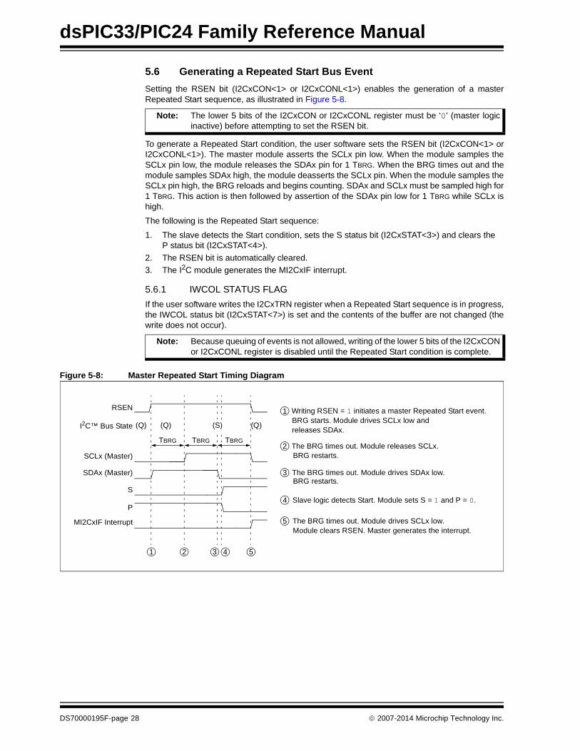
5.6 Generating a Repeated Start Bus Event
Setting the RSEN bit (I2CxCON<1> or I2CxCONL<1>) enables the generation of a masterRepeated Start sequence, as illustrated in Figure 5-8.
To generate a Repeated Start condition, the user software sets the RSEN bit (I2CxCON<1> orI2CxCONL<1>). The master module asserts the SCLx pin low. When the module samples theSCLx pin low, the module releases the SDAx pin for 1 TBRG. When the BRG times out and themodule samples SDAx high, the module deasserts the SCLx pin. When the module samples theSCLx pin high, the BRG reloads and begins counting. SDAx and SCLx must be sampled high for1 TBRG. This action is then followed by assertion of the SDAx pin low for 1 TBRG while SCLx ishigh.
The following is the Repeated Start sequence:
1. The slave detects the Start condition, sets the S status bit (I2CxSTAT<3>) and clears theP status bit (I2CxSTAT<4>).
2. The RSEN bit is automatically cleared.
3. The I2C module generates the MI2CxIF interrupt.
5.6.1 IWCOL STATUS FLAG
If the user software writes the I2CxTRN register when a Repeated Start sequence is in progress,the IWCOL status bit (I2CxSTAT<7>) is set and the contents of the buffer are not changed (thewrite does not occur).
Figure 5-8: Master Repeated Start Timing Diagram
Note: The lower 5 bits of the I2CxCON or I2CxCONL register must be ‘0’ (master logicinactive) before attempting to set the RSEN bit.
Note: Because queuing of events is not allowed, writing of the lower 5 bits of the I2CxCONor I2CxCONL register is disabled until the Repeated Start condition is complete.
The BRG times out. Module releases SCLx. 2BRG restarts.
The BRG times out. Module drives SDAx low.3
Slave logic detects Start. Module sets S = 1 and P = 0.4
I2C™ Bus State (Q)
P
TBRG
(Q)
4
BRG restarts.
The BRG times out. Module drives SCLx low.5Module clears RSEN. Master generates the interrupt.
(Q)releases SDAx.
(S)
DS70000195F-page 28 2007-2014 Microchip Technology Inc.
Inter-Integrated Circuit™ (I2C™)
5.7 Building Complete Master Messages
As described in Section 5.0 “Communicating as a Master in a Single Master Environment”,the user software is responsible for constructing messages with the correct message protocol.The module controls individual portions of the I2C message protocol; however, sequencing of thecomponents of the protocol to construct a complete message is performed by the user software.
The user software can use polling or interrupt methods while using the module. The timingdiagrams shown in this document use interrupts for detecting various events.
The user software can use the SEN, RSEN, PEN, RCEN and ACKEN bits (Least Significant 5 bitsof the I2CxCON or I2CxCONL register) and the TRSTAT status bit as a ‘state’ flag when progressingthrough a message. For example, Table 5-1 shows some example state numbers associated withbus states.
Table 5-1: Master Message Protocol States
The user software will begin a message by issuing a Start condition. The user software will recordthe state number corresponding to the Start.
As each event completes and generates an interrupt, the interrupt handler may check the statenumber. Therefore, for a Start state, the interrupt handler will confirm execution of the Startsequence and then start a master transmission event to send the I2C device address, changingthe state number to correspond to the master transmission.
On the next interrupt, the interrupt handler will again check the state, determining that a mastertransmission just completed. The interrupt handler will confirm successful transmission of thedata, then move on to the next event, depending on the contents of the message. In this manner,on each interrupt, the interrupt handler will progress through the message protocol until thecomplete message is sent.
Figure 5-9 provides a detailed examination of the same message sequence as shown inFigure 5-1. Figure 5-10 provides a few simple examples of the messages using a 7-bit address-ing format. Figure 5-11 provides an example of a 10-bit addressing format message sending datato a slave. Figure 5-12 provides an example of a 10-bit addressing format message receivingdata from a slave.
ExampleState Number(1)
I2CxCON<4:0> or I2CxCONL<4:0>
TRSTAT(I2CxSTAT<14>)
State
0 00000 0 Bus Idle or Wait
1 00001 N/A Sending Start Event
2 00000 1 Master Transmitting
3 00010 N/A Sending Repeated Start Event
4 00100 N/A Sending Stop Event
5 01000 N/A Master Reception
6 10000 N/A Master Acknowledgment
Note 1: The example state numbers are for reference only. The user software can assign the state numbers as desired.
2007-2014 Microchip Technology Inc. DS70000195F-page 29
dsP
IC3
3/PIC
24 F
amily
Re
feren
ce M
an
ual
DS
70
00
01
95
F-p
ag
e 3
0
20
07
-20
14
Micro
chip
Te
chn
olo
gy In
c.
1 2 3 4 5 6 7 8
D3 D2 D1 D0D7 D6 D5 D4
9
N
7 8 9
aster transmission. The data is a re-send of
eception. On interrupt, the user software reads
wledge event. ACKDT = 1 to send a NACK.
p event.
e, but with R/W status bit set, indicating a read.
e RBF status bit.
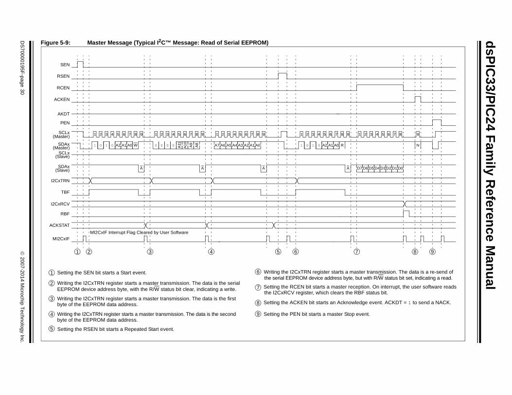
Figure 5-9: Master Message (Typical I2C™ Message: Read of Serial EEPROM)
1 Setting the SEN bit starts a Start event.
AKDT
ACKEN
SEN
SCLx
SDAx
SCLx
SDAx
I2CxTRN
TBF
I2CxRCV
RBF
MI2CxIF
ACKSTAT
1 2 3 4 5 6 7 8
A1 A0
9
A
PEN
RCEN
1 2 3 4 5 6 7 8
A11
A10 A9
A8
1 2 3 4 5 6 7 8 9
W1 1
RSEN
1 2 3 4 5 6 7 8 9
1 32
9
AAA
4 5
2 Writing the I2CxTRN register starts a master transmission. The data is the serial
3 Writing the I2CxTRN register starts a master transmission. The data is the first
4
5
Writing the I2CxTRN register starts a m6
Setting the RCEN bit starts a master r7
9
Setting the ACKEN bit starts an Ackno
Setting the PEN bit starts a master Sto
EEPROM device address byte, with the R/W status bit clear, indicating a write.
Writing the I2CxTRN register starts a master transmission. The data is the secondbyte of the EEPROM data address.
8
Setting the RSEN bit starts a Repeated Start event.
(Master)
(Master)
(Slave)
(Slave)
A3
MI2CxIF Interrupt Flag Cleared by User Software
2
00
7-2
01
4 M
icroch
ip T
ech
no
log
y Inc.
DS
70
00
01
95
F-p
ag
e 3
1
Inte
r-Inte
grated
Circu
it™ (I 2C
™)
Fig
2 3 4 5 6 7 8
D3 D2 D1 D0D6 D5 D4
9
N
98
aster transmission. The data is the
ception.
ledge event. ACKDT = 1 to send a NACK.
p event.
t.
ure 5-10: Master Message (7-Bit Address: Transmission and Reception)
1 Setting the SEN bit starts a Start event.
AKDT
ACKEN
SEN
SCLx
SDAx
SCLx
SDAx
I2CxTRN
TBF
I2CxRCV
RBF
MI2CxIF
ACKSTAT
1 2 3 4 5 6 7 8
A2 A1
9
A
PEN
RCEN
1 2 3 4 5 6 7 8
D7 D6 D5 D4 D3 D2 D1 D0
1 2 3 4 5 6 7 8 9
W
RSEN
1 32
9 1
D7A
4 5 6 7
2 Writing the I2CxTRN register starts a master transmission. The data is the
3 Writing the I2CxTRN register starts a master transmission. The data is the
4 Setting the PEN bit starts a master Stop event.
5 Setting the SEN bit starts a Start event. An interrupt is generated on completion
6 Writing the I2CxTRN register starts a m
7 Setting the RCEN bit starts a master re
8 Setting the ACKEN bit starts an Acknow
Setting the PEN bit starts a master Sto
address byte with the R/W status bit clear.
message byte.
A7 A6 A5 A4 A3
A
A2 A1 RA7 A6 A5 A4 A3
address byte with the R/W status bit se
9
(Master)
(Master)
(Slave)
(Slave)
MI2CxIF Interrupt Flag Cleared by User Software
of the Start event.
dsP
IC3
3/PIC
24 F
amily
Re
feren
ce M
an
ual
DS
70
00
01
95
F-p
ag
e 3
2
20
07
-20
14
Micro
chip
Te
chn
olo
gy In
c.
1 2 3 4 5 6 7 8 9
6 7
r Stop event.
D3 D2 D1 D0D7 D6 D5 D4
A
a master transmission. The data is the second
ts a master transmission. The data is the third
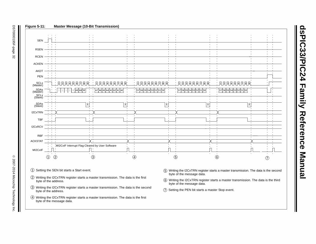
Figure 5-11: Master Message (10-Bit Transmission)
1 Setting the SEN bit starts a Start event.
AKDT
ACKEN
SEN
SCLx
SDAx
SCLx
SDAx
I2CxTRN
TBF
I2CxRCV
RBF
MI2CxIF
ACKSTAT
1 2 3 4 5 6 7 8
A9 A8
9
A
PEN
RCEN
1 2 3 4 5 6 7 8
D3 D2 D1 D0D7 D6 D5 D4A7 A6 A5 A4 A3 A2 A1 A0
1 2 3 4 5 6 7 8 9
W01 1 1 1
RSEN
1 2 3 4 5 6 7 8 9
1 32
9
AAA
4 5
2 Writing the I2CxTRN register starts a master transmission. The data is the first
3 Writing the I2CxTRN register starts a master transmission. The data is the second
4 Writing the I2CxTRN register starts a master transmission. The data is the first
Setting the PEN bit starts a maste
byte of the address.
byte of the message data.
D3 D2 D1 D0D7 D6 D5 D4
5 Writing the I2CxTRN register startsbyte of the message data.
6 Writing the I2CxTRN register starbyte of the message data.
7
(Master)
(Master)
(Slave)
(Slave)
MI2CxIF Interrupt Flag Cleared by User Software
byte of the address.
2
00
7-2
01
4 M
icroch
ip T
ech
no
log
y Inc.
DS
70
00
01
95
F-p
ag
e 3
3
Inte
r-Inte
grated
Circu
it™ (I 2C
™)
Fig
2 3 4 5 6 7 8
D3 D2 D1 D0D6 D5 D4
9
N
9 10
ption. On interrupt, the user software reads
ledge event. ACKDT = 0 to send ACK.
ception.
ledge event. ACKDT = 1 to send NACK.
event.
RBF status bit.
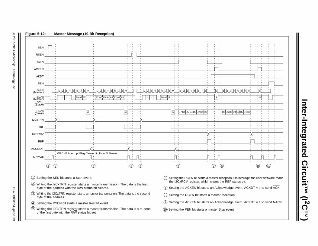
ure 5-12: Master Message (10-Bit Reception)
1 Setting the SEN bit starts a Start event.
AKDT
ACKEN
SEN
SCLx
SDAx
SCLx
SDAx
I2CxTRN
TBF
I2CxRCV
RBF
MI2CxIF
ACKSTAT
1 2 3 4 5 6 7 8
A9 A8
9
A
PEN
RCEN
1 2 3 4 5 6 7 8
D3 D2 D1 D0D7 D6 D5 D4
A7 A6 A5 A4 A3 A2 A1 A0
1 2 3 4 5 6 7 8 9
W01 1 1 1
RSEN
A9 A801 1 1 1 R
1 2 3 4 5 6 7 8 9
1 32
9
A
1
D7AA
4 5 6 7 8
2 Writing the I2CxTRN register starts a master transmission. The data is the first
3 Writing the I2CxTRN register starts a master transmission. The data is the second
4 Setting the RSEN bit starts a master Restart event.
5 Writing the I2CxTRN register starts a master transmission. The data is a re-send
6 Setting the RCEN bit starts a master rece
7 Setting the ACKEN bit starts an Acknow
8 Setting the RCEN bit starts a master re
9 Setting the ACKEN bit starts an Acknow
Setting the PEN bit starts a master Stop
byte of the address with the R/W status bit cleared.
byte of the address.
of the first byte with the R/W status bit set.
the I2CxRCV register, which clears the
(Slave)
(Slave)
(Master)
(Master)
MI2CxIF Interrupt Flag Cleared in User Software
10
dsPIC33/PIC24 Family Reference Manual
6.0 COMMUNICATING AS A MASTER IN A MULTI-MASTER ENVIRONMENT
The I2C protocol allows more than one master to be attached to a system bus. Taking intoaccount that a master can initiate message transactions and generate clocks for the bus, theprotocol has methods to account for situations where more than one master is attempting tocontrol the bus. The clock synchronization ensures that multiple nodes can synchronize theirSCLx clocks to result in one common clock on the SCLx line. The bus arbitration ensures that ifmore than one node attempts a message transaction, only one node will be successful incompleting the message. The other nodes lose bus arbitration and are left with a bus collision.
6.1 Multi-Master Operation
The master module has no special settings to enable the multi-master operation. The moduleperforms the clock synchronization and bus arbitration at all times. If the module is used in asingle master environment, clock synchronization only occurs between the master and slaves,and bus arbitration does not occur.
6.2 Master Clock Synchronization
In a multi-master system, different masters can have different baud rates. The clocksynchronization ensures that when these masters are attempting to arbitrate the bus, their clockswill be coordinated.
The clock synchronization occurs when the master deasserts the SCLx pin (SCLx intended tofloat high). When the SCLx pin is released, the BRG is suspended from counting until the SCLxpin is actually sampled high. When the SCLx pin is sampled high, the BRG is reloaded with thecontents of I2CxBRG<8:0> and begins counting. This ensures that the SCLx high time willalways be at least one BRG rollover count in the event that the clock is held low by an externaldevice, as illustrated in Figure 6-1.
Figure 6-1: Baud Rate Generator Timing with Clock Synchronization
Note: The IPMIEN bit (I2CxCON<11>) should not be set when operating as a master.
SCLx (Slave)
The baud counter decrements twice per TCY. On rollover, the master SCLx will transition.1
1
000 003001002003
SCLx (Master)
001002003000Baud Counter
SDAx (Master)
3 4 6
The slave has pulled SCLx low to initiate a Wait.2
At what would be the master baud counter rollover, detecting SCLx low holds counter.3
Logic samples SCLx once per TCY. Logic detects SCLx high.4
2
The baud counter rollover occurs on next cycle.5
5
On next rollover, the master SCLx will transition.6
TBRG TBRG
TCY
000
DS70000195F-page 34 2007-2014 Microchip Technology Inc.
Inter-Integrated Circuit™ (I2C™)
6.3 Bus Arbitration and Bus Collision
The bus arbitration supports the multi-master system operation. The wired-AND nature of theSDAx line permits arbitration. Arbitration takes place when the first master outputs ‘1’ on SDAxby letting the SDAx float high, and simultaneously, the second master outputs ‘0’ on SDAx bypulling SDAx low. The SDAx signal will go low. In this case, the second master has won busarbitration. The first master has lost bus arbitration, and thus, has a bus collision.
For the first master, the expected data on SDAx is ‘1’, still the data sampled on SDAx is ‘0’. Thisis the definition of a bus collision.
The first master will set the BCL bit (I2CxSTAT<10>) and generates a master (MI2CxIF) or a buscollision (I2CxBCIF) interrupt. The Master module will reset the I2C port to its Idle state.
In multi-master operation, the SDAx line must be monitored for arbitration to see if the signal levelis the expected output level. This check is performed by the master logic, with the result placedin the BCL status bit.
The states where arbitration can be lost are:
• Start condition
• Repeated Start condition
• Address, Data or Acknowledge bit
• Stop condition
6.4 Detecting Bus Collisions and Re-Sending Messages
When a bus collision occurs, the master module sets the BCL status bit and generates a master(MI2CxIF) or a bus collision (I2CxBCIF) interrupt. If a bus collision occurs during a bytetransmission, the transmission is stopped, the TBF status bit is cleared, and the SDAx and SCLxpins are deasserted. If a bus collision occurs during a Start, Repeated Start, Stop or Acknowledgecondition, the condition is aborted, the respective control bits in the I2CxCON register arecleared, and the SDAx and SCLx lines are deasserted.
The user software is expecting an interrupt at the completion of the master event. The usersoftware can check the BCL status bit to determine if the master event completed successfullyor a bus collision occurred (or it may branch to a bus collision interrupt on bus collision), or amaster interrupt occurred in case of a successful master event. If a bus collision occurs, the usersoftware must abort sending the rest of the pending message and prepare to re-send the entiremessage sequence, beginning with the Start condition, after the bus returns to the Idle state. Theuser software can monitor the S and P status bits to wait for an Idle bus. When the user softwareexecutes the master Interrupt Service Routine (ISR) and the I2C bus is free, the user softwarecan resume communication by asserting a Start condition.
6.5 Bus Collision During a Start Condition
Before issuing a Start condition, the user software should verify an Idle state of the bus using theS and P status bits. Two masters may attempt to initiate a message at a similar point in time.Typically, the masters will synchronize clocks and continue arbitration into the message until oneloses arbitration. Any of the following conditions can cause a bus collision to occur during a Start:
• If the SDAx and SCLx pins are at a low logic state at the beginning of the Start condition
• If the SCLx line is at a low logic state before the SDAx line is driven low
In either case, the master that loses arbitration during the Start condition generates a buscollision interrupt.
Note: The bus collision interrupt is not available on all devices. Refer to the specific devicedata sheet for availability.
Note: The bus collision interrupt is not available on all devices. Refer to the specific devicedata sheet for availability.
2007-2014 Microchip Technology Inc. DS70000195F-page 35
dsPIC33/PIC24 Family Reference Manual
6.6 Bus Collision During a Repeated Start Condition
When the two masters do not collide throughout an address byte, a bus collision can occur whenone master attempts to assert a Repeated Start while another transmits data. In this case, themaster generating the Repeated Start loses arbitration and generates a bus collision interrupt.
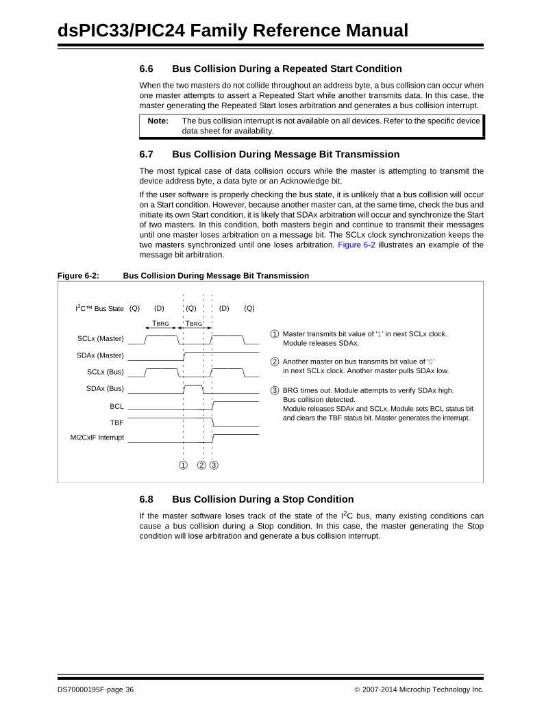
6.7 Bus Collision During Message Bit Transmission
The most typical case of data collision occurs while the master is attempting to transmit thedevice address byte, a data byte or an Acknowledge bit.
If the user software is properly checking the bus state, it is unlikely that a bus collision will occuron a Start condition. However, because another master can, at the same time, check the bus andinitiate its own Start condition, it is likely that SDAx arbitration will occur and synchronize the Startof two masters. In this condition, both masters begin and continue to transmit their messagesuntil one master loses arbitration on a message bit. The SCLx clock synchronization keeps thetwo masters synchronized until one loses arbitration. Figure 6-2 illustrates an example of themessage bit arbitration.
Figure 6-2: Bus Collision During Message Bit Transmission
6.8 Bus Collision During a Stop Condition
If the master software loses track of the state of the I2C bus, many existing conditions cancause a bus collision during a Stop condition. In this case, the master generating the Stopcondition will lose arbitration and generate a bus collision interrupt.
Note: The bus collision interrupt is not available on all devices. Refer to the specific devicedata sheet for availability.
SCLx (Master)
SDAx (Master)
TBF
TBRG
1 2 3
Master transmits bit value of ‘1’ in next SCLx clock.1
TBRG
Module releases SDAx.
Another master on bus transmits bit value of ‘0’ 2in next SCLx clock. Another master pulls SDAx low.
BRG times out. Module attempts to verify SDAx high.3
I2C™ Bus State
BCL
(D)
SCLx (Bus)
SDAx (Bus)
Bus collision detected.Module releases SDAx and SCLx. Module sets BCL status bitand clears the TBF status bit. Master generates the interrupt.
(D)(Q)(Q) (Q)
MI2CxIF Interrupt
DS70000195F-page 36 2007-2014 Microchip Technology Inc.
Inter-Integrated Circuit™ (I2C™)
7.0 COMMUNICATING AS A SLAVE
In some systems, particularly where multiple processors communicate with each other, thedsPIC33/PIC24 device can communicate as a slave, as illustrated in Figure 7-1. When the I2Cmodule is enabled, the slave is active. The slave cannot initiate a message; it can only respondto a message sequence initiated by a master. The master requests a response from a particularslave as defined by the device address byte in the I2C protocol. The slave replies to the masterat the appropriate times as defined by the protocol.
As with the master module, sequencing the components of the protocol for the reply is a usersoftware task. However, the slave detects when the device address matches the addressspecified by the user software for that slave.
Figure 7-1: A Typical Slave I2C™ Message: Multiprocessor Command/Status
After a Start condition, the slave receives and checks the device address. The slave can specifyeither a 7-bit address or a 10-bit address. When a device address is matched, the module willgenerate an interrupt to notify the user software that its device is selected. Based on the R/Wstatus bit sent by the master, the slave either receives or transmits data. If the slave is to receivedata, the slave automatically generates the Acknowledge (ACK), loads the I2CxRCV registerwith the received value currently in the I2CxRSR register and notifies the user software throughan interrupt. If the slave is to transmit data, the user software must load the I2CxTRN register.
7.1 Sampling Receive Data
All the incoming bits are sampled with the rising edge of the clock (SCLx) line.
7.2 Detecting Start and Stop Conditions
The slave detects the Start and the Stop conditions on the bus and indicates that status on the Sstatus bit (I2CxSTAT<3>) and P status bit (I2CxSTAT<4>). The Start (S) and Stop (P) status bitsare cleared when a Reset occurs or when the module is disabled. After detection of a Start orRepeated Start event, the S status bit is set and the P status bit is cleared. After detection of aStop event, the P status bit is set and the S status bit is cleared.
7.2.1 INTERRUPT ON START/REPEATED START AND STOP CONDITIONS (SLAVE MODE)
The user software is notified through a slave interrupt if the SCIE bit (I2CxCONH<5>) is set fora Start/Repeated Start condition or if the PCIE bit (I2CxCONH<6>) is set for a Stop condition.
Bus
MasterSDAx
Sta
rt
FirstAddress Address
Byte
S 111 0 A A 09 8 R P
SlaveSDAx
Activity
N
AAAA
Output
Output
R/W
AC
K
AC
K
AC
KR
est
art
R/W
AC
K
NA
CK
Sto
p
1
Byte
SecondAddress
Byte
A A7 6
A A5 4
A A3 2
A A1 0
CommandDataByte
111 0 A A 19 81
StatusDataByte
10-BitAddress
R
Note: The PCIE and the SCIE bits are not available on all devices. Refer to the specificdevice data sheet for availability.
2007-2014 Microchip Technology Inc. DS70000195F-page 37
dsPIC33/PIC24 Family Reference Manual
7.3 Detecting the Address
Once the module has been enabled, the slave waits for a Start condition to occur. After a Start,depending on the A10M bit (I2CxCON<10> or I2CxCONL<10>), the slave attempts to detect a7-bit or 10-bit address. The slave compares one received byte for a 7-bit address or two receivedbytes for a 10-bit address. A 7-bit address also contains an R/W status bit that specifies the direc-tion of the data transfer after the address. If R/W = 0, a write is specified and the slave receivesdata from the master. If R/W = 1, a read is specified and the slave sends data to the master. The10-bit address contains an R/W status bit; however, by definition, it is always R/W = 0 becausethe slave must receive the second byte of the 10-bit address.
7.3.1 SLAVE ADDRESS MASKING
The I2CxMSK register masks the address bit positions, designating them as “don’t care” bits forboth 10-Bit and 7-Bit Addressing modes. When a bit in the I2CxMSK register is set (= 1), theslave responds when the bit in the corresponding location of the address is a ‘0’ or ‘1’. Forexample, in 7-Bit Slave mode with I2CxMSK = 0100000, the slave module Acknowledgesaddresses, ‘0000000’ and ’0100000’, as valid.
To enable address masking, the IPMI must be disabled by clearing the IPMIEN bit(I2CxCON<11>).
7.3.2 7-BIT ADDRESS AND SLAVE WRITE
After the Start condition, the module shifts 8 bits into the I2CxRSR register, as illustrated inFigure 7-2. The value of the I2CxRSR register is evaluated against that of the I2CxADD andI2CxMSK registers on the falling edge of the eighth clock (SCLx). If the address is valid (that is,an exact match between unmasked bit positions), the following events occur:
• An ACK is generated if the AHEN bit is clear
• The D/A and R/W status bits are cleared
• The module generates the SI2CxIF interrupt on the falling edge of the ninth SCLx clock
Note: The AHEN bit may not be available on all devices. Refer to the specific device datasheet for availability. If this bit is not present, then the device will generate an (ACK)on an address match.
SCLx (Master)
SDAx (Master)
SDAx (Slave)
SI2CxIF Interrupt
4 51 3
Detecting Start bit enables1
I2C™ Bus State (D) (D) (A)(D)
A5A6A7 A4 A3 A2 A1
D/A
ADD10
SCLREL
R/W
address detection. If SCIE is set, then
R/W = 0 indicates that slave 3receives data bytes.
Valid address of first byte clears 4D/A status bit. Slave generates an
R/W status bit cleared. Slave5generates interrupt.
6
Bus waiting. Slave ready to 6receive data.
R/W = 0
(S) (Q)
2
2 User software clears the interrupt flag.(1)
Note 1: The SCIE bit may not be available on all devices. Refer to the specific device data sheet for availability.
the slave interrupt is asserted.(1)
ACK.
DS70000195F-page 38 2007-2014 Microchip Technology Inc.
Inter-Integrated Circuit™ (I2C™)
7.3.3 7-BIT ADDRESS AND SLAVE WRITE WITH THE AHEN AND DHEN BITS
The slave device reception, with the AHEN and DHEN bits set, operates with extra interrupts andclock stretching added after the eighth falling edge of SCLx. These additional interrupts allow theslave software to decide whether it wants to ACK the receive address or data byte, rather thanthe hardware. This functionality adds support for the PMBus™ that was not present on previousversions of this module.
Note: The SI2CxIF interrupt is still set after the ninth falling edge of the SCLx clock, evenif there is no clock stretching and the RBF bit has been cleared. The SI2CxIFinterrupt is not asserted if a NACK is sent to the master.
2007-2014 Microchip Technology Inc. DS70000195F-page 39
dsP
IC3
3/PIC
24 F
amily
Re
feren
ce M
an
ual
DS
70
00
01
95
F-p
ag
e 4
0
20
07
-20
14
Micro
chip
Te
chn
olo
gy In
c.
D2 D1 D0
6 7 8 9
NACK
15
flag.
REL bit. I2CxRCV is loaded with I2CxRSR,f 8th falling edge of SCLx by hardware.
1 Detecting Start bit, enables address detection, interrupt is set if SCEN is set.
3
4
5
9
11
12
RBF is set on the 8th falling clock, address is loaded to I2CxRCV. RBF is asserted.
Interrupt is asserted.
SCLx is stretched low until SCLREL is set.
User software reads the I2CxRCV buffer that clears the RBF flag.
User software releases the SCLx line by writing SCLREL to ‘1’.
Data is loaded into I2CxRCV. RBR
On the 9th falling clock edge, interru
SCLx is stretched and held at low u
User software releases SCLx line b
NACK is received (SCLx is not stre
2
2 User software clears the interrupt flag.
13 Slave recognizes the Stop event.
7
6
8
10
R/W = 0ACK
dsPIC33/PIC24 Family Reference Manual
7.3.4 7-BIT ADDRESS AND SLAVE READ
When a slave read is specified by having R/W = 1 in a 7-bit address byte, the process ofdetecting the device address is similar to that of a slave write, as illustrated in Figure 7-5. If theaddresses match, the following events occur:
• An ACK is generated if the AHEN bit is clear
• The D/A status bit is cleared and the R/W status bit is set
• The module generates the SI2CxIF interrupt on the falling edge of the ninth SCLx clock
Because the slave is expected to reply with data at this point, it is necessary to suspend theoperation of the I2C bus to allow the user software to prepare a response. This is done automaticallywhen the module clears the SCLREL bit. With SCLREL low, the slave will pull down the SCLx clockline, causing a Wait on the I2C bus. The slave and the I2C bus remain in this state until the usersoftware writes the I2CxTRN register with the response data and sets the SCLREL bit.
1 Detecting Start bit, enables address detection, interrupt is set if the SCEN bit is set.
2 User software clears the interrupt flag.
3 Slave receives the address byte with R/W = 1. Hardware clears the SCLREL to suspend master clock. ACKTIM and interrupt flag are asserted.
4 User software clears the interrupt flag.
5 Software reads the I2CxRV register, that clears the RBF flag.
6 ACKDT is written with ACK.
7 User software sets SCLREL to release clock hold. Master clocks in the Acknowledgment sequence. ACKTIM is cleared by hardware.
9 User software clears the interrupt flag.
10 User software loads the I2CxTRN regisindicates that the buffer is full.
11 After last bit, module clears TBF bit, indic
12 At the end of ninth clock, if master senModule does not suspend the clock.
13 Module recognizes Stop event.
8 Hardware clears SCLREL to suspend
dsPIC33/PIC24 Family Reference Manual
7.3.5 10-BIT ADDRESSING MODE
In 10-Bit Addressing mode, the slave must receive two device address bytes, as illustrated inFigure 7-7. The 5 Most Significant bits (MSbs) of the first address byte specify a 10-bit address.The R/W status bit of the address must specify a write, causing the slave device to receive thesecond address byte. For a 10-bit address, the first byte would equal, ‘11110 A9 A8 0’, whereA9 and A8 are the 2 MSbs of the address.
The I2CxMSK register can mask any bit position in a 10-bit address. The 2 MSbs of the I2CxMSKregister are used to mask the MSbs of the incoming address received in the first byte. The remainingbyte of the register is then used to mask the lower byte of the address received in the second byte.
Following the Start condition, the module shifts eight bits into the I2CxRSR register. The value ofthe I2CxRSR<2:1> bits is evaluated against the value of the I2CxADD<9:8> and I2CxMSK<9:8>bits, while the value of the I2CxRSR<7:3> bits is compared to ‘11110’. Address evaluationoccurs on the falling edge of the eighth SCLx clock. For the address to be valid, theI2CxRSR<7:3> bits must be equal to ‘11110’, while the I2CxRSR<2:1> bits must exactly matchany unmasked bits in the I2CxADD<9:8> bits (if both bits are masked, a match is not needed). Ifthe address is valid, the following events occur:
• An ACK is generated• The D/A and R/W status bits are cleared• The module generates the SI2CxIF interrupt on the falling edge of the ninth SCLx clock
The module does generate an interrupt after the reception of the first byte of a 10-bit address;however, this interrupt is of little use.
The module will continue to receive the second byte into the I2CxRSR register. This time, theI2CxRSR<7:0> bits are evaluated against the I2CxADD<7:0> and I2CxMSK<7:0> bits. If thelower byte of the address is valid, as previously described, the following events occur:
• An ACK is generated• The ADD10 status bit is set• The module generates the SI2CxIF interrupt on the falling edge of the ninth SCLx clock• The module will wait for the master to send data or initiate a Repeated Start condition
1 Detecting the Start bit enables address detection; interrupt is set if the SCEN bit is set.
2 User software clears the interrupt flag.
3 Slave receives first address byte. Write indicated. Interrupt flag is asserted. ACKTIM
4 User software clears the interrupt flag.
5 ACKDT is written with ACK by user software.
6 User software sets SCLREL t
7 Slave interrupt is asserted.
8 User software reads I2CxRC
9 Slave Acknowledges the sec
10 User software reads data from
is asserted. If AHEN = 1, slave suspends clock. SCLREL is cleared by hardware.
1 3
4
5
6
7 8 92
dsPIC33/PIC24 Family Reference Manual
7.3.6 SLAVE MODE BUS COLLISION
On a read request from the master, the slave begins shifting data out on the SDAx line. If a buscollision is detected and the SBCDE bit (I2CxCONH<2> register) is set, then the I2CxBCIF bitwill be set. After detecting the bus collision, the slave goes into Idle mode and waits to beaddressed again. User software can use the I2CxBCIF bit or vectors to the bus collision interruptto handle a slave bus collision.
7.3.7 GENERAL CALL OPERATION
The addressing procedure for the I2C bus is such that the first byte after a Start condition usually deter-mines which slave device the master is addressing. The exception is the general call address, whichcan address all devices. When this address is used, all the enabled devices respond with an Acknowl-edge. The general call address is one of the eight addresses reserved for specific purposes by theI2C protocol. It consists of all ‘0’s with R/W = 0. The general call is always a slave write operation.
The general call address is recognized when the General Call Enable bit, GCEN (I2CxCON<7>or I2CxCONL<7>), is set, as illustrated in Figure 7-9. Following a Start bit detect, 8 bits are shiftedinto the I2CxRSR register, and the address is compared against the I2CxADD register and thegeneral call address.
If the general call address matches, the following events occur:
• An ACK is generated• The slave will set the GCSTAT status bit (I2CxSTAT<9>)• The D/A and R/W status bits are cleared• The module generates the SI2CxIF interrupt on the falling edge of the ninth SCLx clock• The I2CxRSR register is transferred to the I2CxRCV register and the RBF status bit
(I2CxSTAT<1>) is set (during the eighth bit)• The module waits for the master to send data
When the interrupt is serviced, the cause for the interrupt can be checked by reading the contents ofthe GCSTAT status bit to determine if the device address was device-specific or a general call address.
Note: The SBCDE and I2CxBCIF bits may not be available on all the devices. Refer to thespecific device data sheet for availability.
Note 1: General call addresses are 7-bit addresses. If configuring the slave for 10-bitaddresses and the A10M and GCEN bits are set, the slave will continue to detectthe 7-bit general call address.
2: The slave will Acknowledge the general call address (7-bit address, 0x00) only ifGCEN is set, and independent of the STRICT and A10M bits.
SCLx (Master)
SDAx (Master)
SDAx (Slave)
SI2CxIF Interrupt
4 51 3
Detecting Start bit enables1I2C™ Bus State (D) (D) (A)(D)
000 0 0 0 0
D/A
I2CxRCV
RBF
R/W
address detection. If SCIE is set,
All ‘0’s and R/W = 0 indicates3a general call.
Valid address clears D/A status bit4and sets GCSTAT status bit.
R/W status bit cleared. Slave 5generates an interrupt.
6
Bus waiting. Slave ready to6receive data.
GCSTAT
Slave generates ACK. Addressloaded into I2CxRCV register.
R/W = 0
(Q)
2
then interrupt will be asserted.(1)
Note 1: The SCIE bit may not be available in all the devices. Refer to the specific device data sheet for availability.
2 User software clears the interruptflag.(1)
(S)
DS70000195F-page 46 2007-2014 Microchip Technology Inc.
Inter-Integrated Circuit™ (I2C™)
7.3.8 RECEIVING ALL ADDRESSES (IPMI OPERATION)
Some I2C system protocols require a slave to act upon all messages on the bus. For example,the IPMI bus uses the I2C nodes as message repeaters in a distributed network. To allow a nodeto repeat all messages, the slave must accept all messages, regardless of the device address.
To enable the IPMI mode, set the IPMIEN bit (I2CxCON<11>) as illustrated in Figure 7-10.Regardless of the state of the A10M and GCEN bits or the value loaded in the I2CxADD register,all addresses are accepted. This includes all valid 7-bit addresses, general call, Start byte, Cbus,reserved and HS modes, and 10-bit address preambles.
Regardless of contents, byte2address is matched.Address match clears D/A status bit.
R/W status bit is set/clear. Slave3generates interrupt.
4
Bus is waiting. 4
Slave generates an ACK. Addressis loaded into I2CxRCV register.
(S) (Q)
R/W
Note: The user application must clear the IPMIEN bit (I2CxCON<11>) during an I2Cmaster operation and set this bit while acting as an IPMI slave.
2007-2014 Microchip Technology Inc. DS70000195F-page 47
dsPIC33/PIC24 Family Reference Manual
7.3.9 STRICT SUPPORT
The slave module Acknowledges all the addresses, including the reserved addresses, whenSTRICT reserved addressing is not enforced (STRICT = 0). The slave device does notAcknowledge the reserved address space if the STRICT bit (I2CxCONL<11>) is set.
Table 7-1: Slave Response to Reserved Addresses
7.3.10 WHEN AN ADDRESS IS INVALID
If a 7-bit address does not match the contents of the I2CxADD<6:0> bits, the slave will return toan Idle state and ignore any activity on the I2C bus until after the Stop condition.
If the first byte of a 10-bit address does not match the contents of the I2CxADD<9:8> bits, theslave will return to an Idle state and ignore all bus activity until after the Stop condition.
If the first byte of a 10-bit address matches the contents of the I2CxADD<9:8> bits, but thesecond byte of the 10-bit address does not match the I2CxADD<7:0> bits, the slave will returnto an Idle state and ignore all bus activity until after the Stop condition.
STRICT BitI2CxADD
Slave AddressReceived Address
into I2CxRSRSlave Acknowledge
x 0x1F 0x1F ACK
1 0x1F Cbus Address NACK
1 Cbus Address Cbus Address NACK
0 Cbus Address Cbus Address ACK
0 Cbus Address 0x1F NACK
0 0x1F Cbus Address NACK
Note: When the STRICT bit is cleared, the ACK signal is generated, only if the address ismatched, even for reserved addresses. The slave device does not generate an ACKif there is an address mismatch, even if the address is a reserved address. Irrespec-tive of the STRICT bit setting, and the address is reserved or not, an ACK signal isgenerated for a proper address match.
DS70000195F-page 48 2007-2014 Microchip Technology Inc.
Inter-Integrated Circuit™ (I2C™)
7.3.11 ADDRESSES RESERVED FROM MASKING
Even when enabled, there are several addresses that are ignored by the I2C module. For theseaddresses, an Acknowledge will not be issued independent of the mask setting. Theseaddresses are listed in Table 7-2.
Table 7-2: Reserved I2C™ Bus Addresses(3)
7.4 Receiving Data from a Master Device
When the R/W status bit of the device address byte is ‘0’ and an address match occurs, the R/Wstatus bit (I2CxSTAT<2>) is cleared. The slave enters a state waiting for data to be sent by themaster. After the device address byte, the contents of the data byte are defined by the systemprotocol and are only received by the slave.
The slave shifts 8 bits into the I2CxRSR register. On the falling edge of the eighth clock (SCLx),the following events occur:
• The module begins to generate an ACK or NACK.
• The RBF status bit (I2CxSTAT<1>) is set to indicate received data.
• The I2CxRSR register byte is transferred to the I2CxRCV register for access by the user software.
• The D/A status bit is set.
• A slave interrupt is generated. User software can check the status of the I2CxSTAT register to determine the cause of the event and then clear the SI2CxIF interrupt flag.
• The module waits for the next data byte.
7-Bit Address Mode
Slave Address R/W Bit Description
0000 000 0 General Call Address(1)
0000 000 1 Start Byte
0000 001 x Cbus Address
0000 010 x Reserved
0000 011 x Reserved
0000 1xx x HS Mode Master Code
1111 1xx x Reserved
1111 0xx x 10-Bit Slave Upper Byte(2)
Note 1: Address will be Acknowledged only if GCEN = 1.
2: A match on this address can only occur as the upper byte in 10-Bit Addressing mode.
3: These addresses will not be Acknowledged, independent of mask settings and STRICT = 1.
2007-2014 Microchip Technology Inc. DS70000195F-page 49
dsPIC33/PIC24 Family Reference Manual
7.4.1 ACKNOWLEDGE GENERATION
Normally, the slave Acknowledges all the received bytes by sending an ACK on the ninth SCLxclock. If the receive buffer is overrun, the slave does not generate this ACK. The overrun isindicated if either (or both) of the following occur:
• The Receive Buffer Full bit, RBF (I2CxSTAT<1>), was set before the transfer was received
• The Receive Overflow bit, I2COV (I2CxSTAT<6>), was set before the transfer was received
Table 7-3 shows what happens when a data transfer byte is received, given the status of the RBFand I2COV status bits. If the RBF status bit is already set when the slave attempts to transfer tothe I2CxRCV register, the transfer does not occur, but the interrupt is generated and the I2COVstatus bit is set. If both the RBF and I2COV status bits are set, the slave acts similarly. Theshaded cells show the condition where user software did not properly clear the overflowcondition.
Reading the I2CxRCV register clears the RBF status bit. The I2COV status bit is cleared bywriting to a ‘0’ through user software.
If the BOEN bit (I2CxCONH<4>) is set, then the I2COV bit (I2CxSTAT<6>) is ignored. If the RBFbit (I2CxSTAT<1>) is not set, then the ACK is generated for the receive address or data; theI2CxRCV buffer is updated with I2CxRSR.
Table 7-3: Data Transfer Received Byte Actions
7.4.3 WAIT STATES DURING SLAVE RECEPTIONS
When the slave receives a data byte, the master can potentially begin sending the next byteimmediately. This allows the user software controlling the nine slave SCLx clock periods toprocess the previously received byte. If this is not enough time, the slave software may want togenerate a bus Wait period.
The STREN bit (I2CxCON<6> or I2CxCONL<6>) enables a bus Wait to occur on slavereceptions. When STREN = 1 at the falling edge of the ninth SCLx clock of a received byte, theslave clears the SCLREL bit. Clearing the SCLREL bit causes the slave to pull the SCLx line low,initiating a Wait. The SCLx clock of the master and slave will synchronize, as provided inSection 6.2 “Master Clock Synchronization”.
When the user software is ready to resume reception, the user software sets the SCLREL bit.This causes the slave to release the SCLx line and the master resumes clocking.
Note: If the BOEN bit (I2CxCONH<4>) is set, then the I2COV bit (I2CxSTAT<6>) isignored and only the RBF bit (I2CxSTAT<1>) determines whether the module willAcknowledge the message or not.
Status Bits as Data Byte Received
Transfer I2CxRSR to
I2CxRCV
Generate ACK
Generate SI2CxIF Interrupt
(interrupt occurs if enabled)
SetRBF
SetI2COV
BOEN(1) RBF I2COV
x 0 0 Yes Yes Yes Yes No change
x 1 0 No No Yes No change Yes
x 1 1 No No Yes No change Yes
0 0 1 Yes No Yes Yes No change
1 0 1 Yes Yes Yes Yes No change
Legend: Shaded cells show states where the user software did not properly clear the overflow condition.
Note 1: BOEN is not available on all the devices. Refer to the specific device data sheet for availability.
DS70000195F-page 50 2007-2014 Microchip Technology Inc.
Inter-Integrated Circuit™ (I2C™)
7.4.4 EXAMPLE MESSAGES OF SLAVE RECEPTION
Receiving a slave message is an automatic process. The user software handling the slaveprotocol uses the slave interrupt to synchronize to the events.
When the slave detects the valid address, the associated interrupt will notify the user software toexpect a message. On receive data, as each data byte transfers to the I2CxRCV register, aninterrupt notifies the user software to unload the buffer.
Figure 7-11 illustrates a simple receive message. Because it is a 7-bit address message, onlyone interrupt occurs for the address bytes. Then, interrupts occur for each of four data bytes. Atan interrupt, the user software may monitor the status bits, RBF (I2CxSTAT<1>), D/A(I2CxSTAT<5>) and R/W (IC2xSTAT<2>), to determine the condition of the byte received.
Figure 7-12 illustrates a similar message using a 10-bit address. In this case, two bytes arerequired for the address.
Figure 7-13 illustrates a case where the user software does not respond to the received byteand the buffer overruns. On reception of the second byte, the module will automatically NACKthe master transmission. Generally, this causes the master to re-send the previous byte. TheI2COV status bit (I2CxSTAT<6>) indicates that the buffer has overrun. The I2CxRCV registerbuffer retains the contents of the first byte. On reception of the third byte, the buffer is still full,and again, the module will NACK the master. After this, the user software finally reads thebuffer. Reading the buffer will clear the RBF status bit; however, the I2COV status bit remainsset. The user software must clear the I2COV status bit (I2CxSTAT<6>). The next received byteis moved to the I2CxRCV register buffer and the module responds with an ACK.
Figure 7-14 highlights clock stretching while receiving data. In the previous examples, theSTREN bit (I2CxCON<6> or I2CxCONL<6>) is equal to ‘0’, which disables clock stretching onreceive messages. In this example, the user software sets STREN to enable clock stretching.When STREN = 1, the module will automatically clock stretch after each received data byte,allowing the user software more time to move the data from the buffer. If RBF = 1 at the fallingedge of the ninth clock, the module automatically clears the SCLREL bit (I2CxCON<12> orI2CxCONL<12>) and pulls the SCLx bus line low. As shown with the second received databyte, if the user software can read the buffer and clear the RBF status bit before the fallingedge of the ninth clock, the clock stretching will not occur. The user software can also suspendthe bus at any time. By clearing the SCLREL bit, the module pulls the SCLx line low after itdetects the bus SCLx low. The SCLx line remains low, suspending transactions on the bus untilthe SCLREL bit is set.
2007-2014 Microchip Technology Inc. DS70000195F-page 51
dsP
IC3
3/PIC
24 F
amily
Re
feren
ce M
an
ual
DS
70
00
01
95
F-p
ag
e 5
2
20
07
-20
14
Micro
chip
Te
chn
olo
gy In
c.
IEN = 0; AHEN = 0; DHEN = 0;
3 5
D7 D6 D5 D4 D3 D2 D1
1 2 3 4 5 6 7 8 9
A
4 4
w.
D0
Figure 7-11: Slave Message (Write Data to Slave: 7-Bit Address; Address Matches; A10M = 0; GCEN = 0; IPMSTRICT = 0 and BOEN = 0)
1 Slave recognizes Start event; S and P status bits set/clear accordingly.
3 Next byte received before I2CxRCV read by software. I2CxRCV register unchanged.I2COV overflow bit set. Slave generates interrupt. Slave sends NACK for reception.
N
4 Next byte also received be
reception. The master state register unchanged. Slave
D0 D0W D0
5
normally until the module seconditions is met, an additionsend a NACK and set the I
another byte after receiving the transmission with a stopand attempt to retransmit th
is moved to I2CxRCV register and must be read by user software to prevent buffer overflow.
SI2CxIF Cleared by User Software
2
00
7-2
01
4 M
icroch
ip T
ech
no
log
y Inc.
DS
70
00
01
95
F-p
ag
e 5
5
Inte
r-Inte
grated
Circu
it™ (I 2C
™)
Fig IPMIEN = 0; AHEN = 0; DHEN = 0;
S
8 3
e clock.
RBF = 0 at this time.
6D5 D3D2D1
2 3 4 5 6 7 8 9
A
9 5
D4
a clock hold. Module must detect SCLx
se a clock hold.
D0
ure 7-14: Slave Message (Write Data to Slave: 7-Bit Address; Clock Stretching Enabled; A10M = 0; GCEN = 0; STRICT = 0 and BOEN = 0)
1 User software sets the STREN bit to enable clock stretching.
SCLx (Master)
DAx (Master)
SCLx (Slave)
SDAx (Slave)
I2CxTRN
TBF
I2CxRCV
RBF
SI2CxIF
STREN
1 2 3 4 5 6 7 8
A1A0
9
A
D7D6D5D4D3D2D1
1 2 3 4 5 6 7 8 9
32
A
5 3
2 Slave receives address byte. I2CxRCV register is read by user software to
Next received byte is message data. The byte moved to I2CxRCV register, sets RBF.
6 User software sets SCLREL bit to releas
7 Slave does not clear SCLREL because
A6A5A4A3A2
S
P
I2COV
R/W
D/A
D7D6D5D4D3D2D1
1 2 3 4 5 6 7 8 9
A
D7D
1
SCLREL
54 6 71
4 Because RBF = 1 at ninth clock, automatic clock stretch begins.Slave clears SCLREL bit. Slave pulls SCLx line low to stretch clock.
5 User software reads I2CxRCV register. RBF bit clears.
8 User software may clear SCLREL to cause
9 User software may set SCLREL to relea
low before asserting SCLx low.
prevent buffer overflow.
W D0 D0
3
dsPIC33/PIC24 Family Reference Manual
7.5 Sending Data to a Master Device
When the R/W status bit of the incoming device address byte is ‘1’ and an address match occurs,the R/W status bit (I2CxSTAT<2>) is set. At this point, the master device is expecting the slaveto respond by sending a byte of data. The contents of the byte are defined by the system protocoland are only transmitted by the slave.
When the interrupt from the address detection occurs, the user software can write a byte to theI2CxTRN register to start the data transmission.
The slave sets the TBF status bit (I2CxSTAT<0>). The eight data bits are shifted out on the fallingedge of the SCLx input. This ensures that the SDAx signal is valid during the SCLx high time.When all 8 bits have been shifted out, the TBF status bit is cleared.
The slave detects the Acknowledge from the master-receiver on the rising edge of the ninth SCLxclock.
If the SDAx line is low, indicating an ACK, the master is expecting more data and the messageis not complete. The module generates a slave interrupt and the ACKSTAT status bit(I2CxSTAT<15>) can be inspected to determine whether more data is being requested.
A slave interrupt is generated on the falling edge of the ninth SCLx clock. User software mustcheck the status of the I2CxSTAT register and clear the SI2CxIF interrupt flag.
If the SDAx line is high, indicating a NACK, the data transfer is complete. The slave resets andgenerates an interrupt and it waits for detection of the next Start bit.
7.5.1 WAIT STATES DURING SLAVE TRANSMISSIONSDuring a slave transmission message, the master expects return data immediately afterdetection of the valid address with R/W = 1. Because of this, the slave automatically generatesa bus Wait whenever the slave returns data.
The automatic Wait occurs at the falling edge of the ninth SCLx clock of a valid device address byte,or transmitted byte, Acknowledged by the master, indicating expectation of more transmit data.
The slave clears the SCLREL bit (I2CxCON<12> or I2CxCONL<12>). Clearing the SCLREL bitcauses the slave to pull the SCLx line low, initiating a Wait. The SCLx clock of the master andslave will synchronize, as shown in Section 6.2 “Master Clock Synchronization”.
When the user software loads the I2CxTRN register and is ready to resume transmission, theuser software sets the SCLREL bit. This causes the slave to release the SCLx line and themaster resumes clocking.
Note: When the IPMIEN bit (I2CxCON<11>) is equal to ‘1’ (IPMI mode), the I2C moduleassumes that the R/W bit is ‘0’. Therefore, the slave transmission function isdisabled. If the R/W bit is ‘1’, the I2C module will trigger an interrupt. This interruptshould be ignored (that is, the I2C interrupt flags should be cleared) and the I2Cslave transmission event should be aborted.
Note: The user software must provide a delay between writing to the transmit buffer andsetting the SCLREL bit. This delay must be greater than the minimum set up timefor slave transmissions, as specified in the “Electrical Characteristics” chapter ofthe specific device data sheet.
DS70000195F-page 56 2007-2014 Microchip Technology Inc.
Inter-Integrated Circuit™ (I2C™)
7.5.2 EXAMPLE MESSAGES OF SLAVE TRANSMISSION
The slave transmissions for 7-bit address messages are illustrated in Figure 7-15. When theaddress matches and the R/W status bit of the address indicates a slave transmission, themodule automatically initiates clock stretching by clearing the SCLREL bit and generates aninterrupt to indicate a response byte is required. The user software writes the response byte intothe I2CxTRN register. As the transmission completes, the master responds with an ACK. If themaster replies with an ACK, the master expects more data, and the module again clears theSCLREL bit and generates another interrupt. If the master responds with a NACK, no more datais required and the module will not stretch the clock, but will generate an interrupt.
The slave transmissions for 10-bit address messages require the slave to first recognize a 10-bitaddress. Because the master must send two bytes for the address, the R/W status bit in the firstbyte of the address specifies a write. To change the message to a read, the master sends aRepeated Start and repeats the first byte of the address with the R/W status bit specifying a read.At this point, the slave transmission begins as illustrated in Figure 7-16.
2007-2014 Microchip Technology Inc. DS70000195F-page 57
dsP
IC3
3/PIC
24 F
amily
Re
feren
ce M
an
ual
DS
70
00
01
95
F-p
ag
e 5
8
20
07
-20
14
Micro
chip
Te
chn
olo
gy In
c.
3 8
ter has sent an ACK, module clears SCLREL
nd P bits set/clear accordingly.
4
D7D6D5D4D3D2D1
1 2 3 4 5 6 7 8 9
5 7
it, indicating buffer is available for next byte.
s interrupt.
ent a NACK, no more data expected. nd will generate an interrupt.
D0
N
Figure 7-15: Slave Message (Read Data from Slave: 7-Bit Address)
1 Slave recognizes Start event, S and P bits set/clear accordingly.
1 Detecting Start bit, enables address detection, interrupt is set if SCEN is set.
2 User software clears the interrupt flag.
3 Slave receives first address byte. Write Indicated. If AHEN = 1, SCLREL is cleared
4 User software clears the interrupt flag.
5 ACKDT is written with ACK by user software.
7 Hardware stretches the clock
8 User software sets SCLREL t
9 I2CxRCV is loaded with I2CxR
User software sets SCLREL to
User software reads I2CxRCV
1 3 4 5 67
2 98
6 User software sets SCLREL to release the clock hold; ACKTIM is cleared by hardware.
by hardware. ACKTIM and interrupt are asserted.cleared by hardware and ACK
by hardware. After Acknowled
NACK sent by master.
Module recognizes the Stop e
ACK ACK
10 11
10
11
12
13
Inter-Integrated Circuit™ (I2C™)
8.0 CONNECTION CONSIDERATIONS FOR I2C BUS
Because the I2C bus is a wired-AND bus connection, pull-up resistors (RP) on the bus arerequired, as illustrated in Figure 8-1. The series resistors (RS) are optional and are used toimprove the Electrostatic Discharge (ESD) susceptibility.
The values of the resistors, RP and RS, depend on the following parameters:
• Supply voltage
• Bus capacitance
• Number of connected devices (input current + leakage current)
• Input level selection (I2C or System Management Bus (SMBus))
Because the device must be able to pull the bus low against RP, current drawn by RP must begreater than the I/O pin minimum sink current, IOL at VOLMAX, for the device output stage.Equation 8-1 shows the formula for computing the minimum pull-up resistance.
Equation 8-1: Minimum Pull-up Resistance
In a 400 kHz system, a minimum rise time specification of 300 ns exists; in a 100 kHz system,the specification is 1000 ns. Because RP must pull the bus up against the total capacitance, CB,with a maximum rise time of 300 ns to (VDD – 0.7V), the maximum resistance for the pull-up(RPMAX) is computed using the formula as shown in Equation 8-2.
Equation 8-2: Maximum Pull-up Resistance
The maximum value for RS is determined by the desired noise margin for the low level. RS cannotdrop enough voltage to make the device VOL and the voltage across RS more than the maximumVIL. Equation 8-3 shows the formula for computing the maximum value for RS.
Equation 8-3: Maximum Series Resistance
Note: The SCLx clock input must have a minimum high and low time for proper operation.Refer to the “Electrical Characteristics” chapter in the specific device data sheetfor more information on the high and low times of the I2C bus specification, andrequirements of the I2C module and I/O pins.
RPMIN =(VDDMAX – VOLMAX)
IOL
– tRCB * [ln(1 – (VDDMAX – VILMAX))]
RSMAX =(VILMAX – VOLMAX)
IOLMAX
2007-2014 Microchip Technology Inc. DS70000195F-page 61
dsPIC33/PIC24 Family Reference Manual
Figure 8-1: Sample Device Configuration for I2C™ Bus
8.1 Integrated Signal Conditioning
The SCLx and SDAx pins have an input glitch filter. The I2C bus requires this filter in both the100 kHz and 400 kHz systems.
When operating on a 400 kHz bus, the I2C bus specification requires a slew rate control of thedevice pin output. This slew rate control is integrated into the device. If the DISSLW bit(I2CxCON<9> or I2CxCONL<9>) is cleared, the slew rate control is active. For other bus speeds,the I2C bus specification does not require slew rate control and the DISSLW bit should be set.
Some system implementations of I2C buses require different input levels for VILMAX and VIHMIN.In a normal I2C system, VILMAX is 0.3 VDD; VIHMIN is 0.7 VDD. By contrast, in a SMBus system,VILMAX is set at 0.8V, while VIHMIN is set at 2.1V.
The SMEN bit (I2CxCON<8> or I2CxCONL<8>) controls the input levels. Setting SMEN (= 1)changes the input levels to SMBus specifications.
RPRP
VDD + 10%
SDAx
SCLx
CB = 10-400 pF
RSRS
Note: I2C™ devices with input levels related to VDD must have one common supplyline to which the pull-up resistor is also connected.
Device
DS70000195F-page 62 2007-2014 Microchip Technology Inc.
Inter-Integrated Circuit™ (I2C™)
9.0 OPERATION IN POWER-SAVING MODES
9.1 Sleep Mode in Slave Mode
The I2C module can wake-up from Sleep mode on detecting a valid slave address match.Because all bit shifting is done with reference to the external SCLx signal, generated by an I2Cmaster, transmissions and receptions can continue even while in Sleep mode.
9.2 Sleep Mode in Master Mode
If Sleep occurs in the middle of a master transmission, and the state machine is partially into atransmission as the clocks stop, the behavior of the module will be undefined. Similarly, if Sleepoccurs in the middle of a master reception, the module behavior will also be undefined. Thetransmitter and receiver will stop at Sleep when in Master mode. Register contents are notaffected by going into Sleep mode or coming out of Sleep mode; there is no automatic way toprevent Sleep entry if a transmission or reception is pending. The user software mustsynchronize Sleep entry with I2C operation to avoid undefined module behavior.
9.3 When the Device Enters Idle Mode
When the device executes a PWRSAV 1 instruction, the device enters Idle mode. The moduleenters a power-saving state in Idle mode, depending on the I2CSIDL bit (I2CxCON<13> orI2CxCONL<13>). If I2CSIDL = 1, the module enters the Power-Saving mode, similar to actionswhile entering Sleep mode. If I2CSIDL = 0, the module does not enter a Power-Saving mode andcontinues to operate normally.
10.0 PERIPHERAL MODULE DISABLE (PMDX) REGISTERS
The Peripheral Module Disable (PMDx) registers provide a method to disable the I2C modulesby stopping all clock sources supplied to that module. When a peripheral is disabled through theappropriate PMDx control bit, the peripheral is in a minimum power consumption state. Thecontrol and status registers associated with the peripheral are also disabled, so writes to thoseregisters will have no effect and read values will be invalid. A peripheral module is only enabledif the I2CxMD bit in the PMDx register is cleared.
11.0 EFFECTS OF A RESET
A Reset disables the I2C module and terminates any active or pending message activity. Referto the I2Cx Control (I2CxCON or I2CxCONH and I2CxCONL) and I2Cx Status (I2CxSTAT)register definitions (Register 3-1, Register 3-2, Register 3-3 and Register 3-4) for the Resetconditions of those registers.
Note: As per the slave I2C behavior, a slave interrupt is generated only on an addressmatch. Therefore, when an I2C slave is in Sleep mode and it receives a messagefrom the master, the clock required to match the received address is derived fromthe master. Only on an address match, will the interrupt be generated and thedevice can wake-up from Sleep, provided the interrupt has been enabled and anISR has been defined.
Note 1: The I2CxCON or I2CxCONL and I2CxCONH are not available on all devices. Referto the specific device data sheet for availability.
2: In this discussion, ‘Idle’ refers to the CPU power-saving state. The lower case ‘idle’refers to the time when the I2C module is not transferring data on the bus.
2007-2014 Microchip Technology Inc. DS70000195F-page 63
dsPIC33/PIC24 Family Reference Manual
12.0 CONSTANT-CURRENT SOURCE
The constant-current source module is a precision current generator and is used in conjunctionwith an Analog-to-Digital Converter (ADC) to measure the resistance of external resistorsconnected to device pins. A typical use of this peripheral is to set the I2C board address usingresistors, as explained in the following sections.
12.1 Features Overview
The constant-current source module offers the following major features:
• Constant-current generator (10 µA nominal)
• Internal selectable connection to one out of four pins
• Enable/Disable bit
12.2 Module Description
Figure 12-1 shows a functional block diagram of the constant-current source module. It consistsof a precision current generator, with a nominal value of 10 µA. The module can be enabled anddisabled using the ISRCEN bit (ISRCCON<15>). The output of the current generator isinternally connected to one out of four pins. The OUTSEL<2:0> bits (ISRCCON<10:8>) allowselection of the target pin. The current source is calibrated during testing. The calibration valueis stored into the Flash die serialization area, and should be read and transferred to theISRCCON register by the application firmware, before using the peripheral.
Note: The constant-current source module is not available on all devices. Refer to thespecific device data sheet for availability.
ISRC1
ISRC3
MUX
OUTSEL<2:0>
ISRC2
ISRC4
ISRCEN
Constant-Current Source
DS70000195F-page 64 2007-2014 Microchip Technology Inc.
Inter-Integrated Circuit™ (I2C™)
12.3 Module Applications
An end application would enable the user to determine the resistance of a couple of externalresistors that encode in their resistance an address value that the application can use whencommunicating over a communications network. A typical application example is PMBus™.
The user application enables the current source and selects a pin where the current is to bedirected. A resistor is externally connected from this pin to ground. The current flow through theexternal resistor generates a voltage. ADC channels, AN4 through AN7, can be used to read thegenerated voltage. The calculated resistance value of the external resistor can be translated intoa number of bits. Allowing for the current source accuracy, the accuracy of the external resistors,and the accuracy of the ADC, 10 to 12 unique resistance values can be read for each resistor.Therefore, two external resistors in the user’s application circuit can encode 100 to 144 uniquevalues for use as module identification addresses, which allows two device pins to replace devicepins that are binary encoded. This results in a large pin count savings, especially in a low pincount package.
The current source output is nominally 10 µA, and the maximum output voltage that can bereached while still maintaining current regulation is AVDD – 0.5V. Table 12-1 shows someexample resistor values that can be used to encode an address into a resistor. The table usescommon 5% tolerance resistor values, and the chosen values are separated by two standardresistor values, which is approximately a 30% value separation.
Table 12-1: Example PMBus™ Address Encoding
Resistor Voltage Address
13k 130 mV 1
18k 180 mV 2
24k 240 mV 3
33k 330 mV 4
43k 430 mV 5
56k 560 mV 6
75k 750 mV 7
100k 1V 8
130k 1.3V 9
180k 1.8V 10
240k 2.4V 11
Note: Other external resistor values may be used as required by the application. Usingtighter tolerance resistors and reducing the spacing between the values of theresistors will allow more addresses to be encoded into each resistor in theapplication circuit.
2007-2014 Microchip Technology Inc. DS70000195F-page 65
Legend: — = unimplemented, read as ‘0’. Reset values are shown in hexadecimal.
Note 1: These registers and/or bits are not available on all devices. Refer to the specific device data sheet for availability.
Inter-Integrated Circuit™ (I2C™)
14.0 DESIGN TIPS
Question 1: I am operating as a bus master and transmitting data. Why do slave andreceive interrupts keep occurring at the same time?
Answer: The master and slave circuits are independent. The slave will receive events fromthe bus sent by the master.
Question 2: I am operating as a slave and I write data to the I2CxTRN register. Why isthe data not being transmitted?
Answer: The slave enters an automatic Wait when preparing to transmit. Ensure that youset the SCLREL bit to release the I2C clock.
Question 3: How do I tell what state the master module is in?
Answer: Looking at the condition of the SEN, RSEN, PEN, RCEN, ACKEN and TRSTATbits will indicate the state of the master module. If all bits are ‘0’, the module isIdle.
Question 4: Operating as a slave, I receive a byte while STREN = 0. What should theuser software do if it cannot process the byte before the next one isreceived?
Answer: Because STREN was ‘0’, the module did not generate an automatic Wait on thereceived byte. However, the user software may, at any time during the message,set STREN and then clear SCLREL. This will cause a Wait on the nextopportunity to synchronize the SCLx clock.
Question 5: My I2C system is a multi-master system. Why are my messages beingcorrupted when I attempt to send them?
Answer: In a multi-master system, other masters may cause bus collisions. In the ISR forthe master, check the BCL status bit to ensure that the operation completedwithout a collision. If a collision is detected, the message must be re-sent fromthe beginning.
Question 6: My I2C system is a multi-master system. How can I tell when it is okay tobegin a message?
Answer: Check the S status bit. If S = 0, the bus is Idle.
Question 7: I tried to send a Start condition on the bus, then transmit a byte by writingto the I2CxTRN register. The byte did not get transmitted. Why?
Answer: You must wait for each event on the I2C bus to complete before starting the nextone. In this case, you should poll the SEN bit to determine when the Start eventcompleted or wait for the master I2C interrupt before data is written to theI2CxTRN register.
Note: In some devices, a separate bus collision interrupt (I2CxBCIF) is generated insteadof a master event interrupt (MI2CxIF).
2007-2014 Microchip Technology Inc. DS70000195F-page 67
dsPIC33/PIC24 Family Reference Manual
15.0 RELATED APPLICATION NOTES
This section lists application notes that are related to this section of the manual. Theseapplication notes may not be written specifically for the dsPIC33/PIC24 device family, but theconcepts are pertinent and could be used with modification and possible limitations. The currentapplication notes related to the Inter-Integrated Circuit™ (I2C™) module include the following:
Title Application Note #
Use of the SSP Module in the I 2C™ Multi-Master Environment AN578
Using the Mid-Range Enhanced Core PIC16 Devices’ MSSP Module for AN734Slave I2C™ Communication
Using the PICmicro® MSSP Module for Master I2C™ Communications AN735
An I2C™ Network Protocol for Environmental Monitoring AN736
Note: Please visit the Microchip web site (www.microchip.com) for additional applicationnotes and code examples for the dsPIC33/PIC24 family of devices.
DS70000195F-page 68 2007-2014 Microchip Technology Inc.
This is the initial released version of this document.
Revision B (August 2008)
This revision includes the following corrections and updates:
• Updated bit definitions for the ACKSTAT bit (I2CxSTAT<15>) and the D/A bit (I2CxSTAT<5>) in Register 3-4.
• Updated the I2CBRG denominator from 1,111,111 to 10,000,000 in Equation 4-1.
• Updated the I2C clock rate values in Table , removed the table notes and added a general note just after the table.
• Updated the last two paragraphs in Section 3.0 “Control and Status Registers” to clarify the shift of matching address bytes in the I2CxRSR register to the I2CxRCV register.
• Updated Section “” to clarify that the master function is enabled when the SEN bit is set, and when data is loaded into the I2CxTRN register.
• Several sections were updated to clarify NACK status in Slave mode. The affected sections are:
- Section 4.2 “I2C Interrupts”
- Section 7.5 “Sending Data to a Master Device”
- Figure 7-13 through Figure 7-16
• The IPMIEN bit was incorrectly described as the Intelligent Peripheral Management Interface Enable bit. All occurrences have been updated to Intelligent Platform Management Interface bit.
• Updated Section 9.2 “Sleep Mode in Master Mode” to clarify what occurs when entering Sleep mode while transmitting.
• Updated the slave message RBF status bit information in Figure 7-11 through Figure 7-16.
• Additional minor corrections such as language and formatting updates are incorporated throughout the document.
Revision C (November 2009)
This revision includes the following corrections and updates:
• The document was updated to include the PIC24H families of devices
• Added Note 1 to the IPMIEN bit in the I2CxCON register (Register 3-1)
• Updated the bit status to HSC (Hardware Set/Cleared) for the P and S bits in the I2CxSTAT register (Register 3-4)
• Updated the BRG Reload Value Calculation (Equation 4-1)
• Added a shaded note on the SDAx and SCLx pins to Section 2.0 “I2C Bus Characteristics” and Section 8.0 “Connection Considerations for I2C Bus”
• Added a shaded note after the first paragraph in Section 5.0 “Communicating as a Master in a Single Master Environment” and Section 6.0 “Communicating as a Master in a Multi-Master Environment”
• Removed the Actual FSCL column, added the PGD column, and updated the Decimal and Hexadecimal values in the I2C Clock Rates table (Table )
• Added a sentence to the end of the second paragraph and added a shaded note in Section 7.3.8 “Receiving All Addresses (IPMI Operation)”
• Added a shaded note to the first paragraph of Section 7.5 “Sending Data to a Master Device”
• Updated the last sentence of the first paragraph in Section 7.5.2 “Example Messages of Slave Transmission” to clarify that an interrupt will be generated.
• Added a shaded note to Section 9.1 “Sleep Mode in Slave Mode”
2007-2014 Microchip Technology Inc. DS70000195F-page 69
dsPIC33/PIC24 Family Reference Manual
Revision D (April 2011)
This revision includes the following updates:
• Equations:
- Updated Equation 8-1, Equation 8-2 and Equation 8-3
• Figures:
- Updated Figure 5-10
• Notes:
- Removed the note in Section 2.0 “I2C Bus Characteristics”
- Added Note 2 in Section 5.2.1 “Sending a 7-bit Address to the Slave”
- Added Note 2 in Section 5.2.3 “Sending a 10-bit Address to the Slave”
- Added a note in Section 7.5.1 “Wait States During Slave Transmissions”
- Replaced the existing note in Section 8.0 “Connection Considerations for I2C Bus”
- Added Note 1 in Table 13-1
• Registers:
- Updated the bit 12 description in Register 3-1
• Sections:
- Updated Section 8.0 “Connection Considerations for I2C Bus”
• Updated the Family Reference Manual name to dsPIC33F/PIC24H Family Reference Manual
• Additional minor corrections such as language and formatting updates were incorporated throughout the document
Revision E (September 2011)
This revision includes the following updates:
• Figures:
- Added Figure 12-1
• Sections:
- Removed reference to dsPIC30F documentation in Section 2.2.2 “Address Slave”
- Added Section 12.0 “Constant-Current Source”
• Additional minor corrections such as language and formatting updates were incorporated throughout the document
DS70000195F-page 70 2007-2014 Microchip Technology Inc.
Inter-Integrated Circuit™ (I2C™)
Revision F (February 2014)
This revision includes the following updates:
• Sections:
- Updated Section 1.0 “Introduction”
- Updated Section 3.0 “Control and Status Registers”
- Updated Section 4.0 “Enabling I2C Operation”, Section 5.0 “Communicating as a Master in a Single Master Environment”
- Included Section 5.2.2 “STRICT Support in Master Mode”
- Updated Section 6.3 “Bus Arbitration and Bus Collision”, Section 6.4 “Detecting Bus Collisions and Re-Sending Messages”
- Included Section 7.2.1 “Interrupt on Start/Repeated Start and Stop Conditions (Slave Mode)”
- Updated Section 7.3.2 “7-Bit Address and Slave Write”
- Included Section 7.3.3 “7-Bit Address and Slave Write with the AHEN and DHEN Bits”
- Updated Section 7.3.4 “7-Bit Address and Slave Read”
- Included Section 7.3.6 “Slave Mode Bus Collision”
- Updated note in Section 7.3.7 “General Call Operation”
- Included Section 7.3.9 “STRICT Support”
- Note included in Section 5.4 “Acknowledge Generation”
• Additional minor corrections, such as language and formatting updates, were incorporated throughout the document.
2007-2014 Microchip Technology Inc. DS70000195F-page 71
dsPIC33/PIC24 Family Reference Manual
NOTES:
DS70000195F-page 72 2007-2014 Microchip Technology Inc.
Note the following details of the code protection feature on Microchip devices:
• Microchip products meet the specification contained in their particular Microchip Data Sheet.
• Microchip believes that its family of products is one of the most secure families of its kind on the market today, when used in the intended manner and under normal conditions.
• There are dishonest and possibly illegal methods used to breach the code protection feature. All of these methods, to our knowledge, require using the Microchip products in a manner outside the operating specifications contained in Microchip’s Data Sheets. Most likely, the person doing so is engaged in theft of intellectual property.
• Microchip is willing to work with the customer who is concerned about the integrity of their code.
• Neither Microchip nor any other semiconductor manufacturer can guarantee the security of their code. Code protection does not mean that we are guaranteeing the product as “unbreakable.”
Code protection is constantly evolving. We at Microchip are committed to continuously improving the code protection features of ourproducts. Attempts to break Microchip’s code protection feature may be a violation of the Digital Millennium Copyright Act. If such actsallow unauthorized access to your software or other copyrighted work, you may have a right to sue for relief under that Act.
Information contained in this publication regarding deviceapplications and the like is provided only for your convenienceand may be superseded by updates. It is your responsibility toensure that your application meets with your specifications.MICROCHIP MAKES NO REPRESENTATIONS ORWARRANTIES OF ANY KIND WHETHER EXPRESS ORIMPLIED, WRITTEN OR ORAL, STATUTORY OROTHERWISE, RELATED TO THE INFORMATION,INCLUDING BUT NOT LIMITED TO ITS CONDITION,QUALITY, PERFORMANCE, MERCHANTABILITY ORFITNESS FOR PURPOSE. Microchip disclaims all liabilityarising from this information and its use. Use of Microchipdevices in life support and/or safety applications is entirely atthe buyer’s risk, and the buyer agrees to defend, indemnify andhold harmless Microchip from any and all damages, claims,suits, or expenses resulting from such use. No licenses areconveyed, implicitly or otherwise, under any Microchipintellectual property rights.
2007-2014 Microchip Technology Inc.
QUALITY MANAGEMENT SYSTEM CERTIFIED BY DNV
== ISO/TS 16949 ==
Trademarks
The Microchip name and logo, the Microchip logo, dsPIC, FlashFlex, KEELOQ, KEELOQ logo, MPLAB, PIC, PICmicro, PICSTART, PIC32 logo, rfPIC, SST, SST Logo, SuperFlash and UNI/O are registered trademarks of Microchip Technology Incorporated in the U.S.A. and other countries.
FilterLab, Hampshire, HI-TECH C, Linear Active Thermistor, MTP, SEEVAL and The Embedded Control Solutions Company are registered trademarks of Microchip Technology Incorporated in the U.S.A.
Silicon Storage Technology is a registered trademark of Microchip Technology Inc. in other countries.
Analog-for-the-Digital Age, Application Maestro, BodyCom, chipKIT, chipKIT logo, CodeGuard, dsPICDEM, dsPICDEM.net, dsPICworks, dsSPEAK, ECAN, ECONOMONITOR, FanSense, HI-TIDE, In-Circuit Serial Programming, ICSP, Mindi, MiWi, MPASM, MPF, MPLAB Certified logo, MPLIB, MPLINK, mTouch, Omniscient Code Generation, PICC, PICC-18, PICDEM, PICDEM.net, PICkit, PICtail, REAL ICE, rfLAB, Select Mode, SQI, Serial Quad I/O, Total Endurance, TSHARC, UniWinDriver, WiperLock, ZENA and Z-Scale are trademarks of Microchip Technology Incorporated in the U.S.A. and other countries.
SQTP is a service mark of Microchip Technology Incorporated in the U.S.A.
GestIC and ULPP are registered trademarks of Microchip Technology Germany II GmbH & Co. KG, a subsidiary of Microchip Technology Inc., in other countries.
All other trademarks mentioned herein are property of their respective companies.
Microchip received ISO/TS-16949:2009 certification for its worldwide
DS70000195F-page 73
headquarters, design and wafer fabrication facilities in Chandler and Tempe, Arizona; Gresham, Oregon and design centers in California and India. The Company’s quality system processes and procedures are for its PIC® MCUs and dsPIC® DSCs, KEELOQ® code hopping devices, Serial EEPROMs, microperipherals, nonvolatile memory and analog products. In addition, Microchip’s quality system for the design and manufacture of development systems is ISO 9001:2000 certified.
DS70000195F-page 74 2007-2014 Microchip Technology Inc.
AMERICASCorporate Office2355 West Chandler Blvd.Chandler, AZ 85224-6199Tel: 480-792-7200 Fax: 480-792-7277Technical Support: http://www.microchip.com/supportWeb Address: www.microchip.com
AtlantaDuluth, GA Tel: 678-957-9614 Fax: 678-957-1455
Austin, TXTel: 512-257-3370
BostonWestborough, MA Tel: 774-760-0087 Fax: 774-760-0088
ChicagoItasca, IL Tel: 630-285-0071 Fax: 630-285-0075