Interconnect Delay Aware RTL Verilog Bus Architecture Generation for an SoC Kyeong Ryu, Alexandru Talpasanu, Vincent Mooney and Jeffrey Davis School of Electrical and Computer Engineering Georgia Institute of Technology August 2004
Transcript
Interconnect Delay Aware RTL Verilog Bus Architecture Generation for an SoC
Kyeong Ryu, Alexandru Talpasanu, Vincent Mooney and Jeffrey Davis
School of Electrical and Computer EngineeringGeorgia Institute of Technology
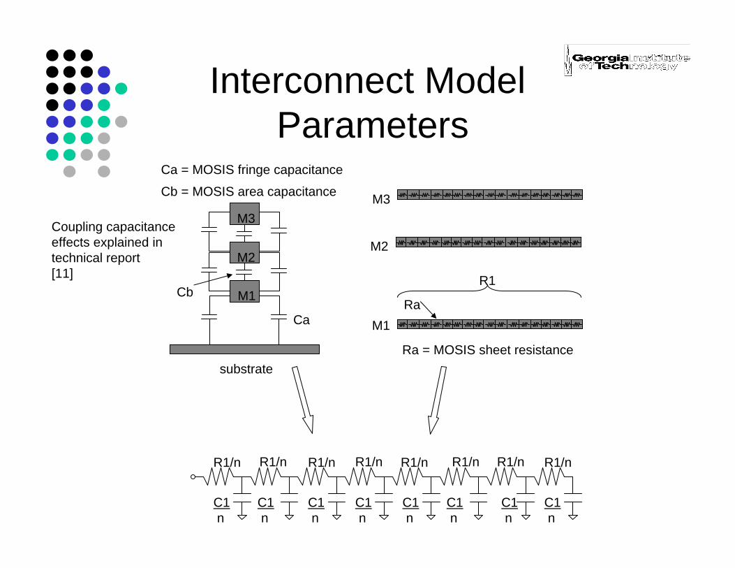
Coupling capacitanceeffects explained in technical report[11]
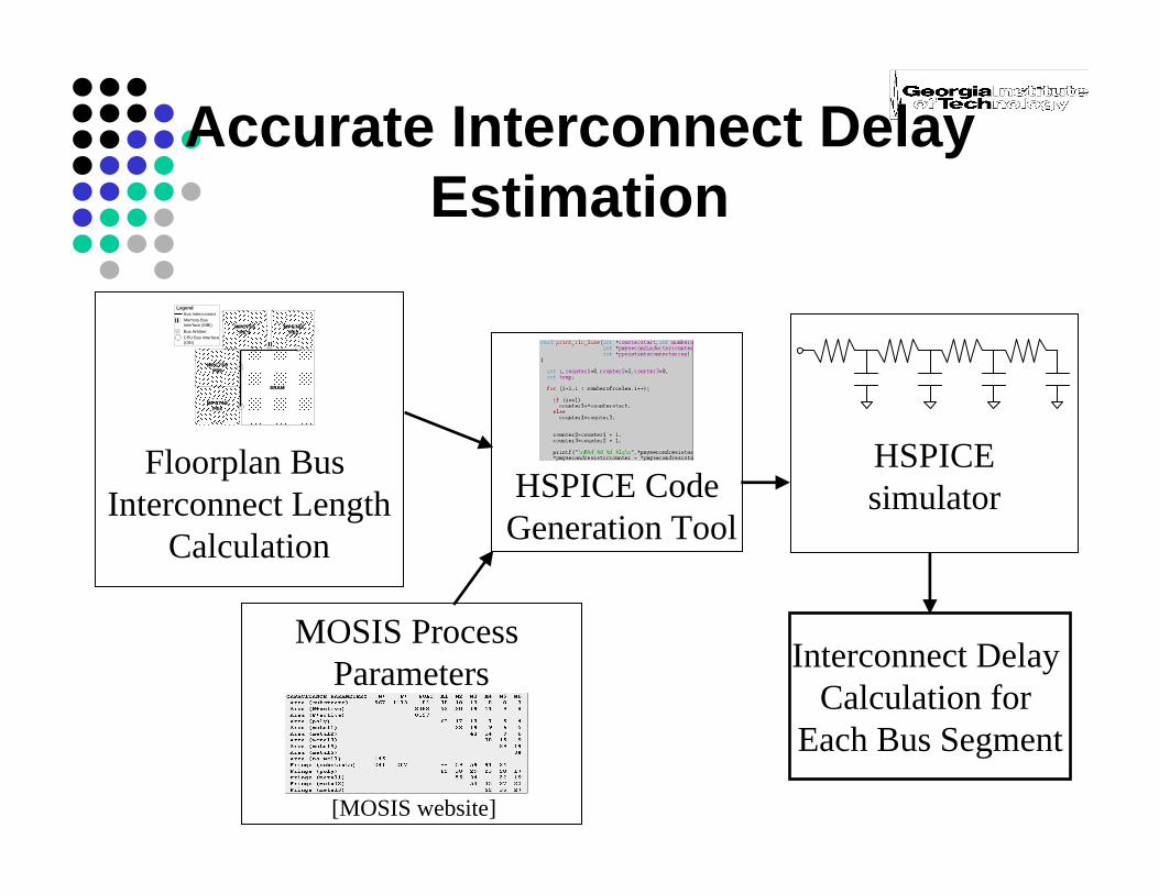
Accurate Interconnect Delay Estimation
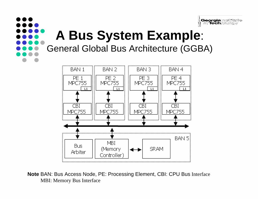
MPC755PE3
SRAMSRAM
MPC755PE1
MPC755PE 2
MPC755PE4
Memory Bus Interface (MBI)Bus Arbitrer
Bus InterconnectLegend
CPU Bus Interface (CBI)
Floorplan Bus Interconnect Length
Calculation
MOSIS Process Parameters
HSPICE CodeGeneration Tool
HSPICEsimulator
Interconnect Delay Calculation for
Each Bus Segment
[MOSIS website]
A Bus System Example:General Global Bus Architecture (GGBA)
Note BAN: Bus Access Node, PE: Processing Element, CBI: CPU Bus InterfaceMBI: Memory Bus Interface
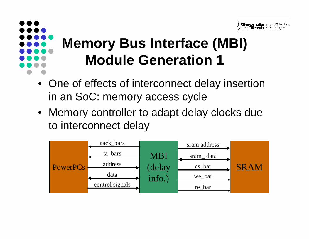
Memory Bus Interface (MBI) Module Generation 1
• One of effects of interconnect delay insertion in an SoC: memory access cycle
• Memory controller to adapt delay clocks due to interconnect delay
PowerPCsMBI
(delayinfo.)
SRAM
aack_bars
ta_bars
address
datacontrol signals
sram_ data
cs_barwe_bar
sram address
re_bar
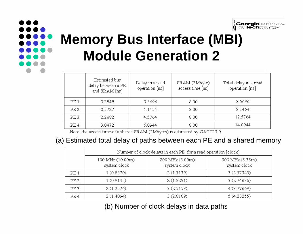
Memory Bus Interface (MBI) Module Generation 2
(a) Estimated total delay of paths between each PE and a shared memory
(b) Number of clock delays in data paths
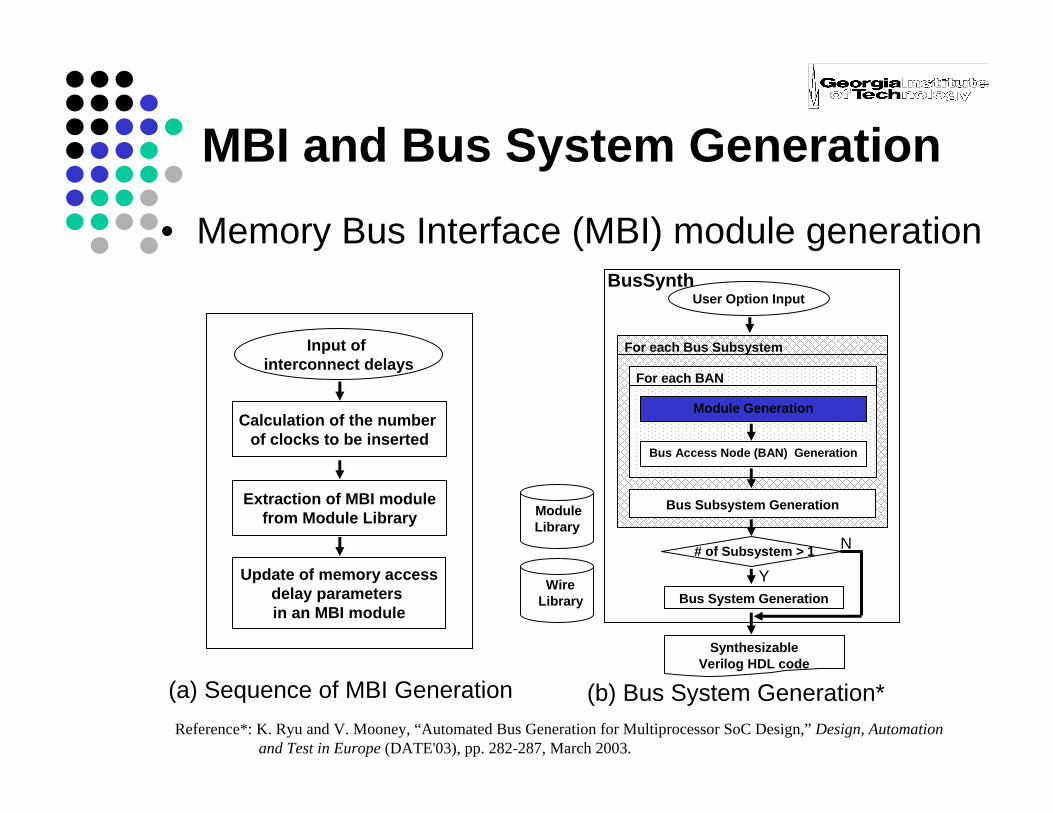
MBI and Bus System Generation
Reference*: K. Ryu and V. Mooney, “Automated Bus Generation for Multiprocessor SoC Design,” Design, Automation and Test in Europe (DATE'03), pp. 282-287, March 2003.
• Memory Bus Interface (MBI) module generation
(a) Sequence of MBI Generation (b) Bus System Generation*
Bus Access Node (BAN) Generation
SynthesizableVerilog HDL code
WireLibrary Bus System Generation
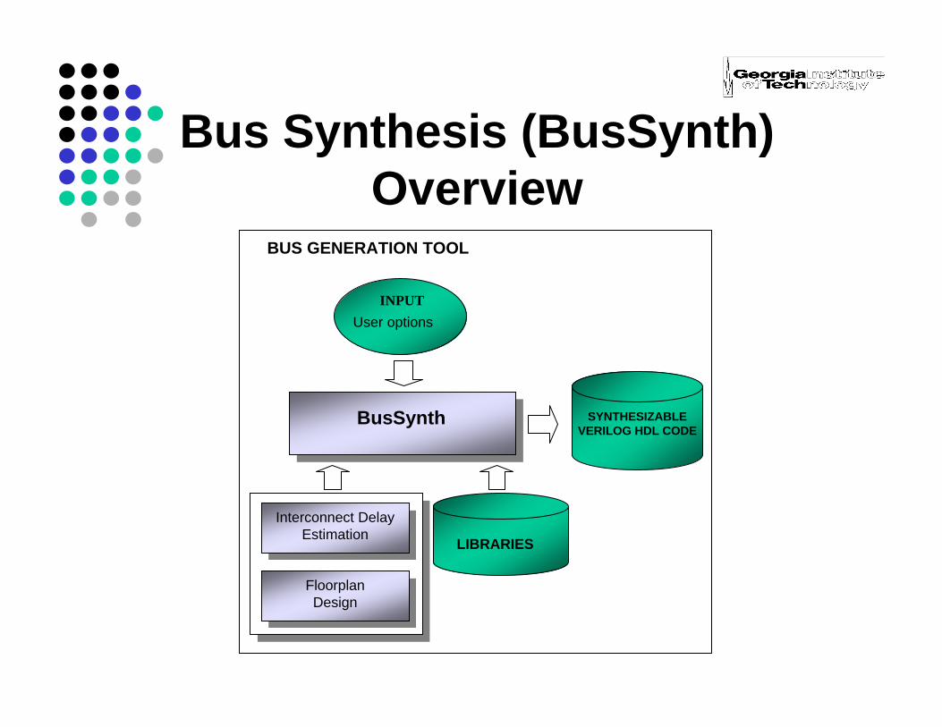
BusSynth
Bus Subsystem Generation
For each Bus Subsystem
# of Subsystem > 1
Y
N
ModuleLibrary
For each BAN
Module Generation
User Option Input
Input of interconnect delays
Calculation of the number of clocks to be inserted
Extraction of MBI modulefrom Module Library
Update of memory accessdelay parameters in an MBI module
A Bus System Generation ExampleUser Input List1. Bus System: # of Bus Subsystems = 12. Bus Subsystem: # of BANs = 53. Bus Properties:
- Bus Subsystem: address bus width = 32 and data bus width: 64
4. BAN Properties:For Bus Subsystem- BAN1: CPU Type = MPC755, non-CPU Type = None
and # of global and local memories = 0- BAN2: CPU Type = MPC755, non-CPU Type = None
and #s of global and local memories = 0- BAN3: CPU Type = MPC755, non-CPU Type = None
and #s of global and local memories = 0- BAN4: CPU Type = MPC755, non-CPU Type = None
and #s of global and local memories = 0- BAN5: CPU Type = None , non-CPU Type = None,
# of global memories = 1, and # of local memories = 05. Memory Properties:
- BAN5: Type = SRAM, address bus width = 21 and data bus width = 64
BAN4BAN3BAN2
SynthesizableVerilog HDL codeSynthesizable
Verilog HDL code
WireLibrary Bus System GenerationBus System Generation
User Option InputUser Option Input
BusSynth
Bus Subsystem GenerationBus Subsystem Generation
For each Subsystem 1
# of Subsystem > 1
Y
N
ModuleLibrary
Bus Subsystem GenerationBus Subsystem Generation
Bus System GenerationBus System GenerationBus System GenerationBus System Generation
MPC755MPC755
CBI_MPC755
CBI_MPC755 CBI_
MPC755
CBI_MPC755
MPC755MPC755 MPC755MPC755
CBI_MPC755
CBI_MPC755 CBI_
MPC755
CBI_MPC755
MPC755MPC755
BAN1
BAN5
Bus Subsystem
Bus System
User Option InputUser Option Input
Bus Subsystem GenerationBus Subsystem Generation
For each Subsystem
Bus Access Node Generation
Bus Access Node Generation
Bus Subsystem GenerationBus Subsystem Generation
# of Subsystem > 1# of Subsystem > 1
Bus System GenerationBus System GenerationSRAMSRAM
Bus Access Node 5 (BAN5) GenerationBus Access NodeGeneration
Bus Access NodeGeneration
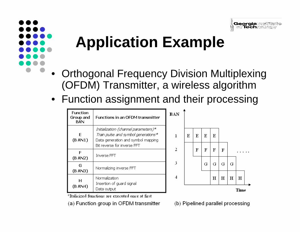
Application Example
• Orthogonal Frequency Division Multiplexing (OFDM) Transmitter, a wireless algorithm
• Function assignment and their processing
Experimental Setup
INPUT
LIBRARIES
SYNTHESIZABLEVERILOG HDL
CODE
User options
BusSynth
VCS SEAMLESSCVE
XRAY
GCC USER C-CODE
BUS GENERATION TOOL SIMULATION ENVIRONMENT
SYNTHESIS ENVIRONMENT
DESIGNCOMPILER
Note: VCS and Design Compiler from Synopsys, Seamless CVE and Xray from Mentor Graphics and GCC fromGNU
Interconnect Delay Estimation
Interconnect Delay Estimation
FloorplanDesign
FloorplanDesign
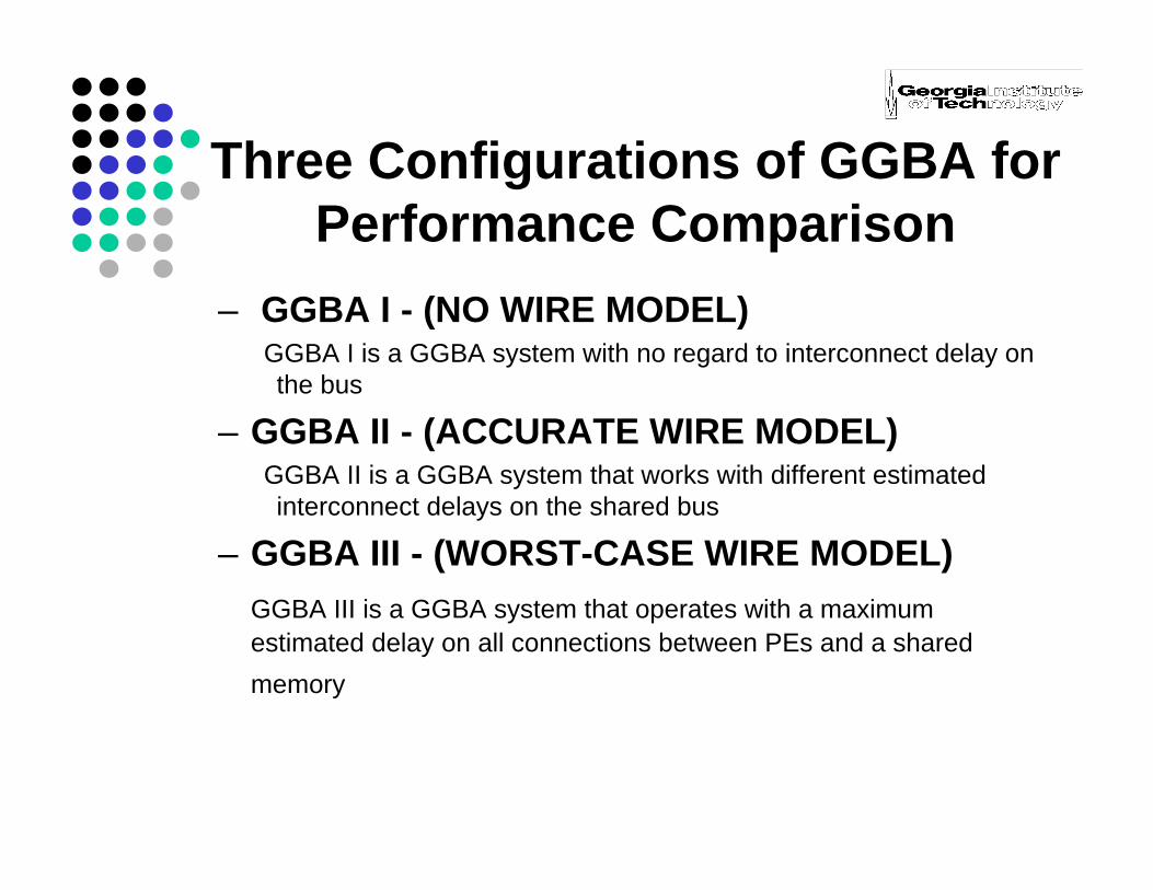
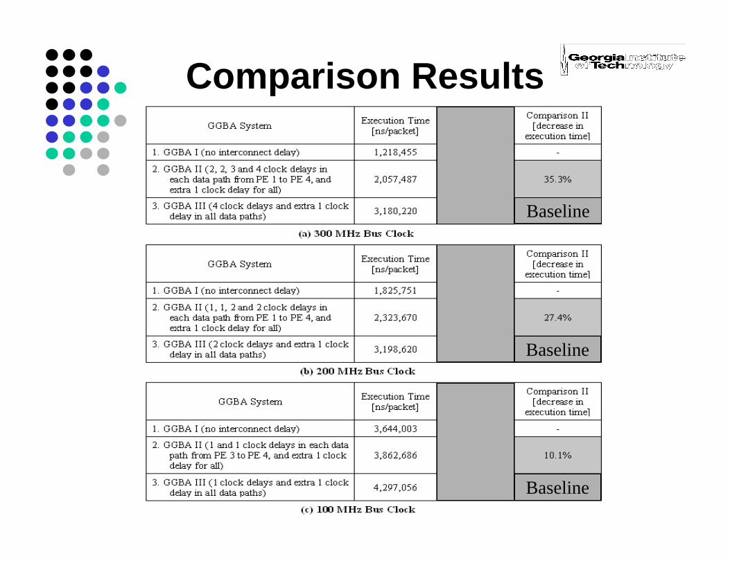
Three Configurations of GGBA for Performance Comparison
– GGBA I - (NO WIRE MODEL) GGBA I is a GGBA system with no regard to interconnect delay on the bus
– GGBA II - (ACCURATE WIRE MODEL) GGBA II is a GGBA system that works with different estimated interconnect delays on the shared bus
– GGBA III - (WORST-CASE WIRE MODEL) GGBA III is a GGBA system that operates with a maximum estimated delay on all connections between PEs and a shared memory
Memory Bus Interface (MBI) Module Generation 2
(a) Estimated total delay of paths between each PE and a shared memory
(b) Number of clock delays in data paths
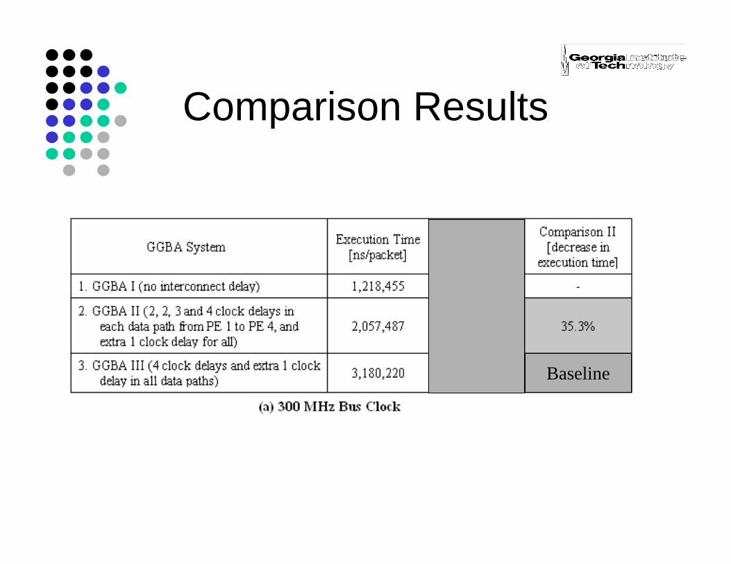
Comparison Results
Baseline
Comparison Results
Baseline
Baseline
Baseline
Conclusion
• Interconnect delay is a major concern as feature size is scaled down
• Interconnect delay estimation from floorplan• Memory Bus Interface (MBI) module and Bus
System generation• Performance improvement due to
interconnect delay aware design• In an OFDM transmitter example, 35.3%